US20040126928A1 - Method for fabricating a chip scale package using wafer level processing and devices resulting therefrom - Google Patents
Method for fabricating a chip scale package using wafer level processing and devices resulting therefromDownload PDFInfo
- Publication number
- US20040126928A1 US20040126928A1US10/624,833US62483303AUS2004126928A1US 20040126928 A1US20040126928 A1US 20040126928A1US 62483303 AUS62483303 AUS 62483303AUS 2004126928 A1US2004126928 A1US 2004126928A1
- Authority
- US
- United States
- Prior art keywords
- active surface
- conductive elements
- channels
- intermediate conductive
- individual die
- Prior art date
- Legal status (The legal status is an assumption and is not a legal conclusion. Google has not performed a legal analysis and makes no representation as to the accuracy of the status listed.)
- Granted
Links
- 238000000034methodMethods0.000titleclaimsdescription35
- 238000012545processingMethods0.000titledescription3
- 239000004065semiconductorSubstances0.000claimsabstractdescription93
- 239000000758substrateSubstances0.000claimsabstractdescription93
- 239000000463materialSubstances0.000claimsabstractdescription42
- 239000008393encapsulating agentSubstances0.000claimsabstractdescription34
- 230000002093peripheral effectEffects0.000claimsabstractdescription11
- 229910000679solderInorganic materials0.000abstractdescription33
- 238000011049fillingMethods0.000abstractdescription3
- 238000002955isolationMethods0.000abstract1
- 235000012431wafersNutrition0.000description21
- 238000004519manufacturing processMethods0.000description15
- 230000008569processEffects0.000description11
- 239000004593EpoxySubstances0.000description9
- 230000015572biosynthetic processEffects0.000description8
- 239000004020conductorSubstances0.000description8
- 238000004806packaging method and processMethods0.000description8
- 238000005538encapsulationMethods0.000description7
- 229910052751metalInorganic materials0.000description6
- 239000002184metalSubstances0.000description6
- RYGMFSIKBFXOCR-UHFFFAOYSA-NCopperChemical compound[Cu]RYGMFSIKBFXOCR-UHFFFAOYSA-N0.000description4
- ATJFFYVFTNAWJD-UHFFFAOYSA-NTinChemical compound[Sn]ATJFFYVFTNAWJD-UHFFFAOYSA-N0.000description4
- 229910045601alloyInorganic materials0.000description4
- 239000000956alloySubstances0.000description4
- 239000010949copperSubstances0.000description4
- 229920001971elastomerPolymers0.000description4
- PCHJSUWPFVWCPO-UHFFFAOYSA-NgoldChemical compound[Au]PCHJSUWPFVWCPO-UHFFFAOYSA-N0.000description4
- 229910052737goldInorganic materials0.000description4
- 239000010931goldSubstances0.000description4
- 238000010438heat treatmentMethods0.000description4
- 229920000642polymerPolymers0.000description4
- 229910052718tinInorganic materials0.000description4
- 238000001721transfer mouldingMethods0.000description4
- 239000000806elastomerSubstances0.000description3
- 125000003700epoxy groupChemical group0.000description3
- 238000005530etchingMethods0.000description3
- 230000009969flowable effectEffects0.000description3
- 239000004615ingredientSubstances0.000description3
- 238000002844meltingMethods0.000description3
- 230000008018meltingEffects0.000description3
- 239000000203mixtureSubstances0.000description3
- 229920000647polyepoxidePolymers0.000description3
- 238000007789sealingMethods0.000description3
- 239000000126substanceSubstances0.000description3
- 229910000881Cu alloyInorganic materials0.000description2
- KDLHZDBZIXYQEI-UHFFFAOYSA-NPalladiumChemical compound[Pd]KDLHZDBZIXYQEI-UHFFFAOYSA-N0.000description2
- 239000004642PolyimideSubstances0.000description2
- BQCADISMDOOEFD-UHFFFAOYSA-NSilverChemical compound[Ag]BQCADISMDOOEFD-UHFFFAOYSA-N0.000description2
- 238000013459approachMethods0.000description2
- 238000003491arrayMethods0.000description2
- 150000001875compoundsChemical class0.000description2
- 239000000356contaminantSubstances0.000description2
- 229910052802copperInorganic materials0.000description2
- 238000000151depositionMethods0.000description2
- 230000008021depositionEffects0.000description2
- 238000013461designMethods0.000description2
- 239000011521glassSubstances0.000description2
- 238000001465metallisationMethods0.000description2
- 150000002739metalsChemical class0.000description2
- 238000001020plasma etchingMethods0.000description2
- 229920001721polyimidePolymers0.000description2
- 229920001296polysiloxanePolymers0.000description2
- 230000009467reductionEffects0.000description2
- 229920005989resinPolymers0.000description2
- 239000011347resinSubstances0.000description2
- 238000000926separation methodMethods0.000description2
- 229910052709silverInorganic materials0.000description2
- 239000004332silverSubstances0.000description2
- XLYOFNOQVPJJNP-UHFFFAOYSA-NwaterSubstancesOXLYOFNOQVPJJNP-UHFFFAOYSA-N0.000description2
- VYZAMTAEIAYCRO-UHFFFAOYSA-NChromiumChemical compound[Cr]VYZAMTAEIAYCRO-UHFFFAOYSA-N0.000description1
- 229910000599Cr alloyInorganic materials0.000description1
- XUIMIQQOPSSXEZ-UHFFFAOYSA-NSiliconChemical compound[Si]XUIMIQQOPSSXEZ-UHFFFAOYSA-N0.000description1
- 238000007792additionMethods0.000description1
- 229910052782aluminiumInorganic materials0.000description1
- XAGFODPZIPBFFR-UHFFFAOYSA-NaluminiumChemical compound[Al]XAGFODPZIPBFFR-UHFFFAOYSA-N0.000description1
- 229910052799carbonInorganic materials0.000description1
- 238000002507cathodic stripping potentiometryMethods0.000description1
- 229910052804chromiumInorganic materials0.000description1
- 239000011651chromiumSubstances0.000description1
- 239000000788chromium alloySubstances0.000description1
- 238000004140cleaningMethods0.000description1
- 238000009833condensationMethods0.000description1
- 230000005494condensationEffects0.000description1
- 229920001940conductive polymerPolymers0.000description1
- 238000011109contaminationMethods0.000description1
- 238000007796conventional methodMethods0.000description1
- 238000005520cutting processMethods0.000description1
- 238000000354decomposition reactionMethods0.000description1
- 230000003247decreasing effectEffects0.000description1
- 230000001419dependent effectEffects0.000description1
- 238000001312dry etchingMethods0.000description1
- 238000001035dryingMethods0.000description1
- 239000000428dustSubstances0.000description1
- 238000001125extrusionMethods0.000description1
- 239000011152fibreglassSubstances0.000description1
- 230000004907fluxEffects0.000description1
- 238000009472formulationMethods0.000description1
- 230000006870functionEffects0.000description1
- 238000007654immersionMethods0.000description1
- 238000011065in-situ storageMethods0.000description1
- 229910052738indiumInorganic materials0.000description1
- APFVFJFRJDLVQX-UHFFFAOYSA-Nindium atomChemical compound[In]APFVFJFRJDLVQX-UHFFFAOYSA-N0.000description1
- 239000012212insulatorSubstances0.000description1
- 239000007788liquidSubstances0.000description1
- 238000012986modificationMethods0.000description1
- 230000004048modificationEffects0.000description1
- 229910052763palladiumInorganic materials0.000description1
- 238000002161passivationMethods0.000description1
- 230000035699permeabilityEffects0.000description1
- 229920002120photoresistant polymerPolymers0.000description1
- 229920002635polyurethanePolymers0.000description1
- 239000004814polyurethaneSubstances0.000description1
- 239000000843powderSubstances0.000description1
- 230000002265preventionEffects0.000description1
- 229910052594sapphireInorganic materials0.000description1
- 239000010980sapphireSubstances0.000description1
- 238000012216screeningMethods0.000description1
- 229910052710siliconInorganic materials0.000description1
- 239000010703siliconSubstances0.000description1
- 239000011856silicon-based particleSubstances0.000description1
- 239000002904solventSubstances0.000description1
- 238000006467substitution reactionMethods0.000description1
- 238000012360testing methodMethods0.000description1
- 239000012808vapor phaseSubstances0.000description1
- 239000011800void materialSubstances0.000description1
- 238000003631wet chemical etchingMethods0.000description1
- -1without limitationChemical class0.000description1
Images


Classifications
- H—ELECTRICITY
- H01—ELECTRIC ELEMENTS
- H01L—SEMICONDUCTOR DEVICES NOT COVERED BY CLASS H10
- H01L24/00—Arrangements for connecting or disconnecting semiconductor or solid-state bodies; Methods or apparatus related thereto
- H01L24/01—Means for bonding being attached to, or being formed on, the surface to be connected, e.g. chip-to-package, die-attach, "first-level" interconnects; Manufacturing methods related thereto
- H01L24/10—Bump connectors ; Manufacturing methods related thereto
- H01L24/12—Structure, shape, material or disposition of the bump connectors prior to the connecting process
- H—ELECTRICITY
- H01—ELECTRIC ELEMENTS
- H01L—SEMICONDUCTOR DEVICES NOT COVERED BY CLASS H10
- H01L21/00—Processes or apparatus adapted for the manufacture or treatment of semiconductor or solid state devices or of parts thereof
- H01L21/02—Manufacture or treatment of semiconductor devices or of parts thereof
- H01L21/04—Manufacture or treatment of semiconductor devices or of parts thereof the devices having potential barriers, e.g. a PN junction, depletion layer or carrier concentration layer
- H01L21/50—Assembly of semiconductor devices using processes or apparatus not provided for in a single one of the groups H01L21/18 - H01L21/326 or H10D48/04 - H10D48/07 e.g. sealing of a cap to a base of a container
- H01L21/56—Encapsulations, e.g. encapsulation layers, coatings
- H01L21/561—Batch processing
- H—ELECTRICITY
- H01—ELECTRIC ELEMENTS
- H01L—SEMICONDUCTOR DEVICES NOT COVERED BY CLASS H10
- H01L21/00—Processes or apparatus adapted for the manufacture or treatment of semiconductor or solid state devices or of parts thereof
- H01L21/02—Manufacture or treatment of semiconductor devices or of parts thereof
- H01L21/04—Manufacture or treatment of semiconductor devices or of parts thereof the devices having potential barriers, e.g. a PN junction, depletion layer or carrier concentration layer
- H01L21/50—Assembly of semiconductor devices using processes or apparatus not provided for in a single one of the groups H01L21/18 - H01L21/326 or H10D48/04 - H10D48/07 e.g. sealing of a cap to a base of a container
- H01L21/56—Encapsulations, e.g. encapsulation layers, coatings
- H01L21/563—Encapsulation of active face of flip-chip device, e.g. underfilling or underencapsulation of flip-chip, encapsulation preform on chip or mounting substrate
- H—ELECTRICITY
- H01—ELECTRIC ELEMENTS
- H01L—SEMICONDUCTOR DEVICES NOT COVERED BY CLASS H10
- H01L23/00—Details of semiconductor or other solid state devices
- H01L23/28—Encapsulations, e.g. encapsulating layers, coatings, e.g. for protection
- H01L23/31—Encapsulations, e.g. encapsulating layers, coatings, e.g. for protection characterised by the arrangement or shape
- H01L23/3107—Encapsulations, e.g. encapsulating layers, coatings, e.g. for protection characterised by the arrangement or shape the device being completely enclosed
- H01L23/3114—Encapsulations, e.g. encapsulating layers, coatings, e.g. for protection characterised by the arrangement or shape the device being completely enclosed the device being a chip scale package, e.g. CSP
- H—ELECTRICITY
- H01—ELECTRIC ELEMENTS
- H01L—SEMICONDUCTOR DEVICES NOT COVERED BY CLASS H10
- H01L23/00—Details of semiconductor or other solid state devices
- H01L23/32—Holders for supporting the complete device in operation, i.e. detachable fixtures
- H—ELECTRICITY
- H01—ELECTRIC ELEMENTS
- H01L—SEMICONDUCTOR DEVICES NOT COVERED BY CLASS H10
- H01L24/00—Arrangements for connecting or disconnecting semiconductor or solid-state bodies; Methods or apparatus related thereto
- H01L24/01—Means for bonding being attached to, or being formed on, the surface to be connected, e.g. chip-to-package, die-attach, "first-level" interconnects; Manufacturing methods related thereto
- H01L24/10—Bump connectors ; Manufacturing methods related thereto
- H01L24/11—Manufacturing methods
- H—ELECTRICITY
- H01—ELECTRIC ELEMENTS
- H01L—SEMICONDUCTOR DEVICES NOT COVERED BY CLASS H10
- H01L24/00—Arrangements for connecting or disconnecting semiconductor or solid-state bodies; Methods or apparatus related thereto
- H01L24/01—Means for bonding being attached to, or being formed on, the surface to be connected, e.g. chip-to-package, die-attach, "first-level" interconnects; Manufacturing methods related thereto
- H01L24/26—Layer connectors, e.g. plate connectors, solder or adhesive layers; Manufacturing methods related thereto
- H01L24/28—Structure, shape, material or disposition of the layer connectors prior to the connecting process
- H—ELECTRICITY
- H01—ELECTRIC ELEMENTS
- H01L—SEMICONDUCTOR DEVICES NOT COVERED BY CLASS H10
- H01L24/00—Arrangements for connecting or disconnecting semiconductor or solid-state bodies; Methods or apparatus related thereto
- H01L24/71—Means for bonding not being attached to, or not being formed on, the surface to be connected
- H01L24/72—Detachable connecting means consisting of mechanical auxiliary parts connecting the device, e.g. pressure contacts using springs or clips
- H—ELECTRICITY
- H01—ELECTRIC ELEMENTS
- H01L—SEMICONDUCTOR DEVICES NOT COVERED BY CLASS H10
- H01L24/00—Arrangements for connecting or disconnecting semiconductor or solid-state bodies; Methods or apparatus related thereto
- H01L24/93—Batch processes
- H01L24/94—Batch processes at wafer-level, i.e. with connecting carried out on a wafer comprising a plurality of undiced individual devices
- H—ELECTRICITY
- H01—ELECTRIC ELEMENTS
- H01L—SEMICONDUCTOR DEVICES NOT COVERED BY CLASS H10
- H01L21/00—Processes or apparatus adapted for the manufacture or treatment of semiconductor or solid state devices or of parts thereof
- H01L21/70—Manufacture or treatment of devices consisting of a plurality of solid state components formed in or on a common substrate or of parts thereof; Manufacture of integrated circuit devices or of parts thereof
- H01L21/77—Manufacture or treatment of devices consisting of a plurality of solid state components or integrated circuits formed in, or on, a common substrate
- H01L21/78—Manufacture or treatment of devices consisting of a plurality of solid state components or integrated circuits formed in, or on, a common substrate with subsequent division of the substrate into plural individual devices
- H—ELECTRICITY
- H01—ELECTRIC ELEMENTS
- H01L—SEMICONDUCTOR DEVICES NOT COVERED BY CLASS H10
- H01L2224/00—Indexing scheme for arrangements for connecting or disconnecting semiconductor or solid-state bodies and methods related thereto as covered by H01L24/00
- H01L2224/01—Means for bonding being attached to, or being formed on, the surface to be connected, e.g. chip-to-package, die-attach, "first-level" interconnects; Manufacturing methods related thereto
- H01L2224/02—Bonding areas; Manufacturing methods related thereto
- H01L2224/023—Redistribution layers [RDL] for bonding areas
- H—ELECTRICITY
- H01—ELECTRIC ELEMENTS
- H01L—SEMICONDUCTOR DEVICES NOT COVERED BY CLASS H10
- H01L2224/00—Indexing scheme for arrangements for connecting or disconnecting semiconductor or solid-state bodies and methods related thereto as covered by H01L24/00
- H01L2224/01—Means for bonding being attached to, or being formed on, the surface to be connected, e.g. chip-to-package, die-attach, "first-level" interconnects; Manufacturing methods related thereto
- H01L2224/02—Bonding areas; Manufacturing methods related thereto
- H01L2224/04—Structure, shape, material or disposition of the bonding areas prior to the connecting process
- H01L2224/05—Structure, shape, material or disposition of the bonding areas prior to the connecting process of an individual bonding area
- H01L2224/0554—External layer
- H01L2224/0556—Disposition
- H01L2224/05568—Disposition the whole external layer protruding from the surface
- H—ELECTRICITY
- H01—ELECTRIC ELEMENTS
- H01L—SEMICONDUCTOR DEVICES NOT COVERED BY CLASS H10
- H01L2224/00—Indexing scheme for arrangements for connecting or disconnecting semiconductor or solid-state bodies and methods related thereto as covered by H01L24/00
- H01L2224/01—Means for bonding being attached to, or being formed on, the surface to be connected, e.g. chip-to-package, die-attach, "first-level" interconnects; Manufacturing methods related thereto
- H01L2224/02—Bonding areas; Manufacturing methods related thereto
- H01L2224/04—Structure, shape, material or disposition of the bonding areas prior to the connecting process
- H01L2224/05—Structure, shape, material or disposition of the bonding areas prior to the connecting process of an individual bonding area
- H01L2224/0554—External layer
- H01L2224/05573—Single external layer
- H—ELECTRICITY
- H01—ELECTRIC ELEMENTS
- H01L—SEMICONDUCTOR DEVICES NOT COVERED BY CLASS H10
- H01L2224/00—Indexing scheme for arrangements for connecting or disconnecting semiconductor or solid-state bodies and methods related thereto as covered by H01L24/00
- H01L2224/01—Means for bonding being attached to, or being formed on, the surface to be connected, e.g. chip-to-package, die-attach, "first-level" interconnects; Manufacturing methods related thereto
- H01L2224/10—Bump connectors; Manufacturing methods related thereto
- H01L2224/12—Structure, shape, material or disposition of the bump connectors prior to the connecting process
- H01L2224/13—Structure, shape, material or disposition of the bump connectors prior to the connecting process of an individual bump connector
- H01L2224/13001—Core members of the bump connector
- H01L2224/1302—Disposition
- H01L2224/13022—Disposition the bump connector being at least partially embedded in the surface
- H—ELECTRICITY
- H01—ELECTRIC ELEMENTS
- H01L—SEMICONDUCTOR DEVICES NOT COVERED BY CLASS H10
- H01L2224/00—Indexing scheme for arrangements for connecting or disconnecting semiconductor or solid-state bodies and methods related thereto as covered by H01L24/00
- H01L2224/01—Means for bonding being attached to, or being formed on, the surface to be connected, e.g. chip-to-package, die-attach, "first-level" interconnects; Manufacturing methods related thereto
- H01L2224/10—Bump connectors; Manufacturing methods related thereto
- H01L2224/12—Structure, shape, material or disposition of the bump connectors prior to the connecting process
- H01L2224/13—Structure, shape, material or disposition of the bump connectors prior to the connecting process of an individual bump connector
- H01L2224/13001—Core members of the bump connector
- H01L2224/1302—Disposition
- H01L2224/13023—Disposition the whole bump connector protruding from the surface
- H—ELECTRICITY
- H01—ELECTRIC ELEMENTS
- H01L—SEMICONDUCTOR DEVICES NOT COVERED BY CLASS H10
- H01L2224/00—Indexing scheme for arrangements for connecting or disconnecting semiconductor or solid-state bodies and methods related thereto as covered by H01L24/00
- H01L2224/01—Means for bonding being attached to, or being formed on, the surface to be connected, e.g. chip-to-package, die-attach, "first-level" interconnects; Manufacturing methods related thereto
- H01L2224/10—Bump connectors; Manufacturing methods related thereto
- H01L2224/12—Structure, shape, material or disposition of the bump connectors prior to the connecting process
- H01L2224/13—Structure, shape, material or disposition of the bump connectors prior to the connecting process of an individual bump connector
- H01L2224/13001—Core members of the bump connector
- H01L2224/13099—Material
- H01L2224/131—Material with a principal constituent of the material being a metal or a metalloid, e.g. boron [B], silicon [Si], germanium [Ge], arsenic [As], antimony [Sb], tellurium [Te] and polonium [Po], and alloys thereof
- H01L2224/13101—Material with a principal constituent of the material being a metal or a metalloid, e.g. boron [B], silicon [Si], germanium [Ge], arsenic [As], antimony [Sb], tellurium [Te] and polonium [Po], and alloys thereof the principal constituent melting at a temperature of less than 400°C
- H01L2224/13116—Lead [Pb] as principal constituent
- H—ELECTRICITY
- H01—ELECTRIC ELEMENTS
- H01L—SEMICONDUCTOR DEVICES NOT COVERED BY CLASS H10
- H01L2224/00—Indexing scheme for arrangements for connecting or disconnecting semiconductor or solid-state bodies and methods related thereto as covered by H01L24/00
- H01L2224/01—Means for bonding being attached to, or being formed on, the surface to be connected, e.g. chip-to-package, die-attach, "first-level" interconnects; Manufacturing methods related thereto
- H01L2224/10—Bump connectors; Manufacturing methods related thereto
- H01L2224/15—Structure, shape, material or disposition of the bump connectors after the connecting process
- H01L2224/16—Structure, shape, material or disposition of the bump connectors after the connecting process of an individual bump connector
- H—ELECTRICITY
- H01—ELECTRIC ELEMENTS
- H01L—SEMICONDUCTOR DEVICES NOT COVERED BY CLASS H10
- H01L2224/00—Indexing scheme for arrangements for connecting or disconnecting semiconductor or solid-state bodies and methods related thereto as covered by H01L24/00
- H01L2224/01—Means for bonding being attached to, or being formed on, the surface to be connected, e.g. chip-to-package, die-attach, "first-level" interconnects; Manufacturing methods related thereto
- H01L2224/26—Layer connectors, e.g. plate connectors, solder or adhesive layers; Manufacturing methods related thereto
- H01L2224/27—Manufacturing methods
- H01L2224/274—Manufacturing methods by blanket deposition of the material of the layer connector
- H—ELECTRICITY
- H01—ELECTRIC ELEMENTS
- H01L—SEMICONDUCTOR DEVICES NOT COVERED BY CLASS H10
- H01L2224/00—Indexing scheme for arrangements for connecting or disconnecting semiconductor or solid-state bodies and methods related thereto as covered by H01L24/00
- H01L2224/01—Means for bonding being attached to, or being formed on, the surface to be connected, e.g. chip-to-package, die-attach, "first-level" interconnects; Manufacturing methods related thereto
- H01L2224/26—Layer connectors, e.g. plate connectors, solder or adhesive layers; Manufacturing methods related thereto
- H01L2224/28—Structure, shape, material or disposition of the layer connectors prior to the connecting process
- H01L2224/29—Structure, shape, material or disposition of the layer connectors prior to the connecting process of an individual layer connector
- H01L2224/29001—Core members of the layer connector
- H01L2224/29099—Material
- H01L2224/291—Material with a principal constituent of the material being a metal or a metalloid, e.g. boron [B], silicon [Si], germanium [Ge], arsenic [As], antimony [Sb], tellurium [Te] and polonium [Po], and alloys thereof
- H01L2224/29101—Material with a principal constituent of the material being a metal or a metalloid, e.g. boron [B], silicon [Si], germanium [Ge], arsenic [As], antimony [Sb], tellurium [Te] and polonium [Po], and alloys thereof the principal constituent melting at a temperature of less than 400°C
- H01L2224/29111—Tin [Sn] as principal constituent
- H—ELECTRICITY
- H01—ELECTRIC ELEMENTS
- H01L—SEMICONDUCTOR DEVICES NOT COVERED BY CLASS H10
- H01L2224/00—Indexing scheme for arrangements for connecting or disconnecting semiconductor or solid-state bodies and methods related thereto as covered by H01L24/00
- H01L2224/73—Means for bonding being of different types provided for in two or more of groups H01L2224/10, H01L2224/18, H01L2224/26, H01L2224/34, H01L2224/42, H01L2224/50, H01L2224/63, H01L2224/71
- H01L2224/732—Location after the connecting process
- H01L2224/73201—Location after the connecting process on the same surface
- H01L2224/73203—Bump and layer connectors
- H—ELECTRICITY
- H01—ELECTRIC ELEMENTS
- H01L—SEMICONDUCTOR DEVICES NOT COVERED BY CLASS H10
- H01L2224/00—Indexing scheme for arrangements for connecting or disconnecting semiconductor or solid-state bodies and methods related thereto as covered by H01L24/00
- H01L2224/80—Methods for connecting semiconductor or other solid state bodies using means for bonding being attached to, or being formed on, the surface to be connected
- H01L2224/81—Methods for connecting semiconductor or other solid state bodies using means for bonding being attached to, or being formed on, the surface to be connected using a bump connector
- H01L2224/812—Applying energy for connecting
- H01L2224/8121—Applying energy for connecting using a reflow oven
- H—ELECTRICITY
- H01—ELECTRIC ELEMENTS
- H01L—SEMICONDUCTOR DEVICES NOT COVERED BY CLASS H10
- H01L2224/00—Indexing scheme for arrangements for connecting or disconnecting semiconductor or solid-state bodies and methods related thereto as covered by H01L24/00
- H01L2224/80—Methods for connecting semiconductor or other solid state bodies using means for bonding being attached to, or being formed on, the surface to be connected
- H01L2224/81—Methods for connecting semiconductor or other solid state bodies using means for bonding being attached to, or being formed on, the surface to be connected using a bump connector
- H01L2224/812—Applying energy for connecting
- H01L2224/8122—Applying energy for connecting with energy being in the form of electromagnetic radiation
- H—ELECTRICITY
- H01—ELECTRIC ELEMENTS
- H01L—SEMICONDUCTOR DEVICES NOT COVERED BY CLASS H10
- H01L2224/00—Indexing scheme for arrangements for connecting or disconnecting semiconductor or solid-state bodies and methods related thereto as covered by H01L24/00
- H01L2224/80—Methods for connecting semiconductor or other solid state bodies using means for bonding being attached to, or being formed on, the surface to be connected
- H01L2224/81—Methods for connecting semiconductor or other solid state bodies using means for bonding being attached to, or being formed on, the surface to be connected using a bump connector
- H01L2224/818—Bonding techniques
- H01L2224/81801—Soldering or alloying
- H01L2224/81815—Reflow soldering
- H—ELECTRICITY
- H01—ELECTRIC ELEMENTS
- H01L—SEMICONDUCTOR DEVICES NOT COVERED BY CLASS H10
- H01L2224/00—Indexing scheme for arrangements for connecting or disconnecting semiconductor or solid-state bodies and methods related thereto as covered by H01L24/00
- H01L2224/80—Methods for connecting semiconductor or other solid state bodies using means for bonding being attached to, or being formed on, the surface to be connected
- H01L2224/83—Methods for connecting semiconductor or other solid state bodies using means for bonding being attached to, or being formed on, the surface to be connected using a layer connector
- H01L2224/838—Bonding techniques
- H01L2224/8385—Bonding techniques using a polymer adhesive, e.g. an adhesive based on silicone, epoxy, polyimide, polyester
- H01L2224/83851—Bonding techniques using a polymer adhesive, e.g. an adhesive based on silicone, epoxy, polyimide, polyester being an anisotropic conductive adhesive
- H—ELECTRICITY
- H01—ELECTRIC ELEMENTS
- H01L—SEMICONDUCTOR DEVICES NOT COVERED BY CLASS H10
- H01L2224/00—Indexing scheme for arrangements for connecting or disconnecting semiconductor or solid-state bodies and methods related thereto as covered by H01L24/00
- H01L2224/93—Batch processes
- H01L2224/94—Batch processes at wafer-level, i.e. with connecting carried out on a wafer comprising a plurality of undiced individual devices
- H—ELECTRICITY
- H01—ELECTRIC ELEMENTS
- H01L—SEMICONDUCTOR DEVICES NOT COVERED BY CLASS H10
- H01L24/00—Arrangements for connecting or disconnecting semiconductor or solid-state bodies; Methods or apparatus related thereto
- H01L24/80—Methods for connecting semiconductor or other solid state bodies using means for bonding being attached to, or being formed on, the surface to be connected
- H01L24/81—Methods for connecting semiconductor or other solid state bodies using means for bonding being attached to, or being formed on, the surface to be connected using a bump connector
- H—ELECTRICITY
- H01—ELECTRIC ELEMENTS
- H01L—SEMICONDUCTOR DEVICES NOT COVERED BY CLASS H10
- H01L24/00—Arrangements for connecting or disconnecting semiconductor or solid-state bodies; Methods or apparatus related thereto
- H01L24/80—Methods for connecting semiconductor or other solid state bodies using means for bonding being attached to, or being formed on, the surface to be connected
- H01L24/83—Methods for connecting semiconductor or other solid state bodies using means for bonding being attached to, or being formed on, the surface to be connected using a layer connector
- H—ELECTRICITY
- H01—ELECTRIC ELEMENTS
- H01L—SEMICONDUCTOR DEVICES NOT COVERED BY CLASS H10
- H01L2924/00—Indexing scheme for arrangements or methods for connecting or disconnecting semiconductor or solid-state bodies as covered by H01L24/00
- H01L2924/0001—Technical content checked by a classifier
- H01L2924/00013—Fully indexed content
- H—ELECTRICITY
- H01—ELECTRIC ELEMENTS
- H01L—SEMICONDUCTOR DEVICES NOT COVERED BY CLASS H10
- H01L2924/00—Indexing scheme for arrangements or methods for connecting or disconnecting semiconductor or solid-state bodies as covered by H01L24/00
- H01L2924/01—Chemical elements
- H01L2924/01005—Boron [B]
- H—ELECTRICITY
- H01—ELECTRIC ELEMENTS
- H01L—SEMICONDUCTOR DEVICES NOT COVERED BY CLASS H10
- H01L2924/00—Indexing scheme for arrangements or methods for connecting or disconnecting semiconductor or solid-state bodies as covered by H01L24/00
- H01L2924/01—Chemical elements
- H01L2924/01006—Carbon [C]
- H—ELECTRICITY
- H01—ELECTRIC ELEMENTS
- H01L—SEMICONDUCTOR DEVICES NOT COVERED BY CLASS H10
- H01L2924/00—Indexing scheme for arrangements or methods for connecting or disconnecting semiconductor or solid-state bodies as covered by H01L24/00
- H01L2924/01—Chemical elements
- H01L2924/01013—Aluminum [Al]
- H—ELECTRICITY
- H01—ELECTRIC ELEMENTS
- H01L—SEMICONDUCTOR DEVICES NOT COVERED BY CLASS H10
- H01L2924/00—Indexing scheme for arrangements or methods for connecting or disconnecting semiconductor or solid-state bodies as covered by H01L24/00
- H01L2924/01—Chemical elements
- H01L2924/01024—Chromium [Cr]
- H—ELECTRICITY
- H01—ELECTRIC ELEMENTS
- H01L—SEMICONDUCTOR DEVICES NOT COVERED BY CLASS H10
- H01L2924/00—Indexing scheme for arrangements or methods for connecting or disconnecting semiconductor or solid-state bodies as covered by H01L24/00
- H01L2924/01—Chemical elements
- H01L2924/01029—Copper [Cu]
- H—ELECTRICITY
- H01—ELECTRIC ELEMENTS
- H01L—SEMICONDUCTOR DEVICES NOT COVERED BY CLASS H10
- H01L2924/00—Indexing scheme for arrangements or methods for connecting or disconnecting semiconductor or solid-state bodies as covered by H01L24/00
- H01L2924/01—Chemical elements
- H01L2924/01033—Arsenic [As]
- H—ELECTRICITY
- H01—ELECTRIC ELEMENTS
- H01L—SEMICONDUCTOR DEVICES NOT COVERED BY CLASS H10
- H01L2924/00—Indexing scheme for arrangements or methods for connecting or disconnecting semiconductor or solid-state bodies as covered by H01L24/00
- H01L2924/01—Chemical elements
- H01L2924/01046—Palladium [Pd]
- H—ELECTRICITY
- H01—ELECTRIC ELEMENTS
- H01L—SEMICONDUCTOR DEVICES NOT COVERED BY CLASS H10
- H01L2924/00—Indexing scheme for arrangements or methods for connecting or disconnecting semiconductor or solid-state bodies as covered by H01L24/00
- H01L2924/01—Chemical elements
- H01L2924/01047—Silver [Ag]
- H—ELECTRICITY
- H01—ELECTRIC ELEMENTS
- H01L—SEMICONDUCTOR DEVICES NOT COVERED BY CLASS H10
- H01L2924/00—Indexing scheme for arrangements or methods for connecting or disconnecting semiconductor or solid-state bodies as covered by H01L24/00
- H01L2924/01—Chemical elements
- H01L2924/01049—Indium [In]
- H—ELECTRICITY
- H01—ELECTRIC ELEMENTS
- H01L—SEMICONDUCTOR DEVICES NOT COVERED BY CLASS H10
- H01L2924/00—Indexing scheme for arrangements or methods for connecting or disconnecting semiconductor or solid-state bodies as covered by H01L24/00
- H01L2924/01—Chemical elements
- H01L2924/0105—Tin [Sn]
- H—ELECTRICITY
- H01—ELECTRIC ELEMENTS
- H01L—SEMICONDUCTOR DEVICES NOT COVERED BY CLASS H10
- H01L2924/00—Indexing scheme for arrangements or methods for connecting or disconnecting semiconductor or solid-state bodies as covered by H01L24/00
- H01L2924/01—Chemical elements
- H01L2924/01079—Gold [Au]
- H—ELECTRICITY
- H01—ELECTRIC ELEMENTS
- H01L—SEMICONDUCTOR DEVICES NOT COVERED BY CLASS H10
- H01L2924/00—Indexing scheme for arrangements or methods for connecting or disconnecting semiconductor or solid-state bodies as covered by H01L24/00
- H01L2924/01—Chemical elements
- H01L2924/01082—Lead [Pb]
- H—ELECTRICITY
- H01—ELECTRIC ELEMENTS
- H01L—SEMICONDUCTOR DEVICES NOT COVERED BY CLASS H10
- H01L2924/00—Indexing scheme for arrangements or methods for connecting or disconnecting semiconductor or solid-state bodies as covered by H01L24/00
- H01L2924/01—Chemical elements
- H01L2924/01087—Francium [Fr]
- H—ELECTRICITY
- H01—ELECTRIC ELEMENTS
- H01L—SEMICONDUCTOR DEVICES NOT COVERED BY CLASS H10
- H01L2924/00—Indexing scheme for arrangements or methods for connecting or disconnecting semiconductor or solid-state bodies as covered by H01L24/00
- H01L2924/013—Alloys
- H01L2924/0132—Binary Alloys
- H—ELECTRICITY
- H01—ELECTRIC ELEMENTS
- H01L—SEMICONDUCTOR DEVICES NOT COVERED BY CLASS H10
- H01L2924/00—Indexing scheme for arrangements or methods for connecting or disconnecting semiconductor or solid-state bodies as covered by H01L24/00
- H01L2924/013—Alloys
- H01L2924/014—Solder alloys
- H—ELECTRICITY
- H01—ELECTRIC ELEMENTS
- H01L—SEMICONDUCTOR DEVICES NOT COVERED BY CLASS H10
- H01L2924/00—Indexing scheme for arrangements or methods for connecting or disconnecting semiconductor or solid-state bodies as covered by H01L24/00
- H01L2924/10—Details of semiconductor or other solid state devices to be connected
- H01L2924/1015—Shape
- H01L2924/10155—Shape being other than a cuboid
- H01L2924/10157—Shape being other than a cuboid at the active surface
- H—ELECTRICITY
- H01—ELECTRIC ELEMENTS
- H01L—SEMICONDUCTOR DEVICES NOT COVERED BY CLASS H10
- H01L2924/00—Indexing scheme for arrangements or methods for connecting or disconnecting semiconductor or solid-state bodies as covered by H01L24/00
- H01L2924/10—Details of semiconductor or other solid state devices to be connected
- H01L2924/11—Device type
- H01L2924/12—Passive devices, e.g. 2 terminal devices
- H01L2924/1204—Optical Diode
- H01L2924/12042—LASER
- H—ELECTRICITY
- H01—ELECTRIC ELEMENTS
- H01L—SEMICONDUCTOR DEVICES NOT COVERED BY CLASS H10
- H01L2924/00—Indexing scheme for arrangements or methods for connecting or disconnecting semiconductor or solid-state bodies as covered by H01L24/00
- H01L2924/10—Details of semiconductor or other solid state devices to be connected
- H01L2924/11—Device type
- H01L2924/14—Integrated circuits
- H—ELECTRICITY
- H01—ELECTRIC ELEMENTS
- H01L—SEMICONDUCTOR DEVICES NOT COVERED BY CLASS H10
- H01L2924/00—Indexing scheme for arrangements or methods for connecting or disconnecting semiconductor or solid-state bodies as covered by H01L24/00
- H01L2924/15—Details of package parts other than the semiconductor or other solid state devices to be connected
- H01L2924/151—Die mounting substrate
- H01L2924/1515—Shape
- H01L2924/15153—Shape the die mounting substrate comprising a recess for hosting the device
- H—ELECTRICITY
- H01—ELECTRIC ELEMENTS
- H01L—SEMICONDUCTOR DEVICES NOT COVERED BY CLASS H10
- H01L2924/00—Indexing scheme for arrangements or methods for connecting or disconnecting semiconductor or solid-state bodies as covered by H01L24/00
- H01L2924/15—Details of package parts other than the semiconductor or other solid state devices to be connected
- H01L2924/151—Die mounting substrate
- H01L2924/15165—Monolayer substrate
- H—ELECTRICITY
- H01—ELECTRIC ELEMENTS
- H01L—SEMICONDUCTOR DEVICES NOT COVERED BY CLASS H10
- H01L2924/00—Indexing scheme for arrangements or methods for connecting or disconnecting semiconductor or solid-state bodies as covered by H01L24/00
- H01L2924/15—Details of package parts other than the semiconductor or other solid state devices to be connected
- H01L2924/151—Die mounting substrate
- H01L2924/156—Material
- H01L2924/1579—Material with a principal constituent of the material being a polymer, e.g. polyester, phenolic based polymer, epoxy
- H—ELECTRICITY
- H10—SEMICONDUCTOR DEVICES; ELECTRIC SOLID-STATE DEVICES NOT OTHERWISE PROVIDED FOR
- H10D—INORGANIC ELECTRIC SEMICONDUCTOR DEVICES
- H10D62/00—Semiconductor bodies, or regions thereof, of devices having potential barriers
- H10D62/10—Shapes, relative sizes or dispositions of the regions of the semiconductor bodies; Shapes of the semiconductor bodies
- H10D62/117—Shapes of semiconductor bodies
Definitions
- the present inventionrelates to semiconductor devices and methods for fabricating semiconductor devices. More specifically, the invention relates to a method for packaging a semiconductor die having conductive elements that protrude at least to the surface of a covering or encapsulation of the die active surface.
- a single semiconductor die or chip including a plurality of integrated circuits on an active surface thereofis typically mounted within a sealed package of a silicon-filled epoxy formed thereabout by a process known as transfer-molding.
- the packagegenerally protects the die from physical damage and from contaminants, such as moisture or chemicals, found in the surrounding environment.
- the packagealso provides a lead system for connecting the electrical devices (integrated circuits) formed on the die to a printed circuit board or other higher-level packaging.
- Conductive bumpsmay comprise metals or alloys including, without limitation, conventional tin ⁇ lead solders, or may comprise conductive or conductor-filled epoxies, all as known in the art. Formation of the conductive bumps used in these applications can be accomplished using a variety of commonly known methods, such as deposition onto bond pads by screening or printing, preform ball or bump placement, or ball bumping using wire bonding equipment to form each individual bump in situ.
- a widely practiced way to increase the number of available input/output (I/O) connections for a dieis to use flip-chip methodology for packaging, where an array of conductive elements (e.g., conductive bumps, ball bonds, conductive pillars or other conductive structures) is positioned on the active surface or circuit face of the die, which is then mounted active surface down upon a single chip or multi-chip module carrier substrate.
- conductive elementse.g., conductive bumps, ball bonds, conductive pillars or other conductive structures
- a flip-chip or bumped (raised) dieis a semiconductor chip (die) having bumps formed on bond pads on the active surface or front side of the die, the bumps being used as electrical and mechanical connectors to conductors of higher level packaging, such as a PCB or other carrier substrate.
- the bumped dieis inverted (flipped) and bonded to trace ends or other terminals on a carrier substrate by means of the bumps.
- diverse materialsare conventionally used to form the bumps on the die, such as solder, conductive polymers, and conductor-filled polymers.
- solder segmentsare deposited on the die and then reflowed to form a substantially spherical shape, and subsequently reheated to form a solder joint between the bond pads on the so-called flip-chip and terminal pads on the carrier substrate, the solder joint providing both electrical and mechanical connections between the flip-chip and substrate.
- the encapsulated IC dieis removed from the mold and mounted to tab tape or a PCB, with the nonsubmerged portions of the towers providing an electrical connection thereto.
- chip scale packagesor “CSPs”
- CSPssemiconductor packages of compact size
- an improved method for forming chip scale packagesthat have a uniform encapsulant extending from edge to edge of the active surface to provide a substantially hermetic seal across the entire active surface and over exposed edges of the layer or layers of integrated circuitry formed thereon.
- an improved method for forming a chip scale packagethat does not significantly complicate the manufacturing or handling of the integrated circuitry and that is repeatable and reliable when using conventional mass production manufacturing techniques.
- the chip scale packagecould be substantially formed during and simultaneously with the fabrication of the die itself in wafer form.
- the present inventionincludes a method of forming a semiconductor device by forming or providing a semiconductor wafer having an active surface defining a large plurality of individual die locations thereon.
- waferincludes traditional wafer structures as well as silicon-on-insulator (SOI), silicon-on-glass (SOG) and silicon-on-sapphire (SOS) substrates, among other semiconductor substrates known in the art.
- SOIsilicon-on-insulator
- SOGsilicon-on-glass
- SOSsilicon-on-sapphire
- Either the bond padsare provided with intermediate conductive elements thereon or the input/output connections provided by the bond pads are redistributed into a different pattern or array using traces over the active surface, and the intermediate conductive elements formed at the redistributed input/output locations.
- a grid of channels or troughsis formed, as by scribing with a wafer saw or etching, between die locations and of sufficient depth to pass through the active surface to an insulative region to isolate individual, adjacent die active surface regions on the semiconductor wafer.
- a flowable material used to encapsulate at least the active surface of the entire semiconductor waferis applied thereto to cover the intermediate conductive elements and is then planarized to expose the intermediate conductive elements.
- the flowable encapsulant materialextends into the channel regions, sealing the exposed, lateral edges of the active surface surrounding each individual die location.
- the intermediate conductive elementsare then provided with external conductive elements projecting transversely from the surface of the encapsulant layer, or an anisotropically-conductive (so-called “Z-axis”) film may be placed over the substrate.
- conductive tracesmay be formed to extend between the exposed ends of the intermediate conductive elements and one or more edges of each die location to form one or more rows of edge connects suitable for DCA to a carrier substrate.
- the semiconductor waferis cut through its entire depth, as with a wafer saw, along the centers of the channel regions to separate, or “singulate,” the individual die locations into flip-chip or DCA dice to be individually connected to a carrier substrate.
- the entire semiconductor substrate or a group of unsingulated dicemay be mated to a carrier substrate and bonded thereto using the external conductive elements.
- the exposed ends of intermediate conductive elementsalone may be employed as a land grid array for attachment of a die, substrate segment or entire semiconductor substrate to a bumped carrier substrate, and may optionally be provided with larger conductive pads thereover to facilitate connection to the carrier substrate bumps.
- conductive tracescan be extended from the bond pads across the active surface and down channel side walls between at least some of the individual die locations prior to encapsulation of the active surface of the semiconductor substrate, the trace ends then being exposed during singulation of the dice to form rows of electrical contacts along edges of the singulated dice, or groups of dice which remain together.
- FIGS. 1 A- 1 Fillustrate cross-sectional views of the process steps used in carrying out the method of the present invention
- FIG. 2depicts a singulated die with an active surface conformally covered by an encapsulant material
- FIG. 3illustrates a cross-sectional view of an alternative structural embodiment of the invention
- FIG. 4depicts a group of unsingulated semiconductor devices applied to a carrier substrate
- FIG. 5depicts alternative cross-sectional shapes of channels or troughs between die locations
- FIG. 6depicts a top plan view of a plurality of dice laid out on a semiconductor wafer where the channels or troughs have been formed along streets between individual die locations;
- FIGS. 7A and 7Bdepict a portion of a semiconductor substrate having two adjacent dice with traces extending over a channel or trough therebetween to provide a DCA configuration upon singulation and a singulated die in a DCA configuration with a carrier substrate;
- FIG. 8depicts a computer system incorporating a microprocessor or a memory device, or both, which incorporates a chip scale package manufactured according to the present invention.
- FIGS. 1 A- 1 FA fabrication process of the invention is depicted in FIGS. 1 A- 1 F, which figures include a semiconductor substrate 10 having a plurality of bond pads 12 on an active surface 14 thereof, bearing at least one layer 16 of integrated circuitry 18 thereon.
- FIGS. 1 A- 1 Felements common to FIGS. 1 A- 1 F will hereinafter be numbered identically in subsequent figures illustrating other preferred methods according to the present invention.
- Semiconductor substrate 10may comprise a wafer, as defined above, including a plurality of individual die locations thereon.
- the bond pads 12are “bumped” with intermediate conductive elements 20 which project upwardly from active surface 14 , or some or all of the input ⁇ output locations for each die are redistributed using conductive traces prior to being bumped, such processes being well known in the art. If the external conductive elements (see below) are metallurgically incompatible with bond pads 12 , the intermediate conductive elements 20 may be of a layer or layers of metals which will provide a better metallurgical bond therebetween.
- intermediate conductive elements 20of three superimposed layers (top to bottom) of copper, copper/chromium alloy, and chromium. It is also contemplated that the bond pads 12 may be bumped using a wire bonding capillary, or with solder of a higher melting temperature than that of another solder to be employed in external conductive elements 32 , as referenced below. Intermediate conductive elements 20 may also comprise a conductive or conductor-filled epoxy, such as a silver-filled epoxy.
- intermediate conductive elements 20The only significant constraints on the material and configuration selected for intermediate conductive elements 20 are compatibility with the bond pads 12 or other input/output contacts on substrate 10 as well as with external conductive elements 32 , and sufficient temperature tolerance and physical strength to withstand encapsulation of active surface 14 of substrate 10 and formation of external conductive elements 32 thereon.
- a preferred semiconductor substrate 10has a standardized number of bond pads or other input/output locations 12 for every die location (the term “bond pad” as used herein also encompassing redistributed input/output locations), the bond pads 12 being located in arrays, one array for each die location, with bond pads 12 laterally spaced from one another at, for example, a uniform pitch.
- the arraysare positioned at specific locations relative to a reference point (not shown) of the semiconductor substrate 10 , in order to facilitate precise relative positioning of semiconductor substrate 10 and processing equipment therefor. This reference point may include the side edge of semiconductor substrate 10 or a center line of substrate 10 (not shown).
- the number, pitch and array configuration of bond pads 12may be nonstandardized, for example, if different input/output arrangements are desired for dice formed on the same substrate 10 .
- FIG. 1Bdepicts how a plurality of channels or troughs 26 is formed on the active surface 14 of semiconductor substrate 10 to define individual die locations on substrate 10 .
- the term “individual dice”specifically includes, without limitation, partial wafers bearing more than one die as well as single dice.
- Channels or troughs 26extend at a depth sufficient enough to pass entirely through the at least one layer 16 of integrated circuitry 18 upon the active surface 14 of substrate 10 and are cut in a grid pattern comprising a first group of mutually parallel channels or troughs 26 which are arranged perpendicular to a second group of mutually parallel channels or troughs 26 .
- the channels or troughs 26are located to extend along the so-called “streets” between individual semiconductor die locations on substrate 10 , wherein neither active or passive components of integrated circuitry 18 , or interconnect structures for same, are typically located.
- Various types of methodsmay be utilized to form channels or troughs 26 having different cross-sectional configurations.
- a beveled or chamfered channel as shownmay be formed using a wafer saw blade or an isotropic etch.
- a laser drillmay be used to form a parallel-sided channel, while an etching process, such as dry or plasma etching or wet solution etching, may be used to form channels with either substantially parallel sides or sloped sides, depending upon the anisotropic or isotropic tendencies of the etch employed.
- a flowable encapsulant material 30may be placed across the entire surface of semiconductor substrate 10 to such a depth as to entirely cover intermediate conductive elements 20 , the encapsulant material also filling channels or troughs 26 . This is depicted in FIG. 1C.
- One preferred method of applying encapsulant material 30 to active surface 14 of substrate 10is the previously mentioned transfer molding, wherein a mold having a cavity configured to receive substrate 10 with a void above active surface 14 of a depth or height at least as great as the height of intermediate conductive elements 20 is injected with a molten, silicon particle-filled epoxy.
- Transfer-moldingis typically only effected on a plurality of singulated dice secured to a lead frame strip, with each die residing in an individual cavity having lead fingers of an associated lead frame extending therefrom, the lead fingers subsequently being severed from the lead frame strip and bent to a final configuration in a so-called “trim and form” operation.
- the transfer molding of an entire semiconductor substrate such as a waferis also believed to be novel and to comprise part of the present invention.
- Encapsulant material 30may also comprise an epoxy compound molded in an open or closed mold cavity over the active surface 14 of substrate 10 , or may be selected from a dispensed epoxy or polyimide as well known to those skilled in the art for encapsulation or sealing of semiconductor dice.
- Suitable materials for use as an encapsulant materialpreferably exhibit low moisture permeability, nonconductivity (i.e., having low ionic contamination), good thermal conductivity, high physical resilience, and a low coefficient of thermal expansion (CTE).
- Preferred materialsinclude polymers as a general class and, specifically, filled polymers, epoxies, silicones, silicone-carbon resins, polyimides and polyurethanes, as well as glasses. It should be again noted that the filling of channels or troughs 26 with encapsulant material 30 results in the substantially hermetic sealing of exposed peripheral edges of the at least one layer 16 of integrated circuitry 18 on the active surface 14 .
- external conductive elements designated generally as 32are formed or placed on each intermediate conductive element 20 .
- External conductive elementsmay, for example, comprise segments of solder paste stenciled or screen printed onto intermediate conductive elements 20 , preformed solder balls, conductive or conductor-filled epoxies, or anisotropically conductive films or segments of such films.
- solder paste form(rather than as preformed, already-reflowed balls)
- a proper amount of solder paste per segmentshould be used to adequately cover the intermediate conductive elements 20 , to remain tacky without slumping, and to create a ball having sufficient size for the intended application when the solder paste is reflowed.
- Suitable solder pastes for use with the instant processcan comprise any combination of chemical components that produces paste properties resulting in the desired chemical and physical characteristics for application (e.g., bonding characteristics and viscosity), reflow, cleaning, and formation of the final, encapsulated, raised ball-bond semiconductor structure.
- the selected solder pasteshould be able to substantially retain the original printed or dot-dispensed pattern at room temperature and during reflow.
- the solder pasteshould, when reflowed as described hereafter, uniformly coalesce to a substantially spherical ball that is substantially free of surrounding small satellite balls.
- the solder pasteis a low-melting-point alloy, usually of lead (Pb) and tin (Sn), that can wet copper, conduct current, and mechanically join conductors and the like.
- Pblead
- Sntin
- suitable ingredients for use as a solder pasteinclude, without limitation, aluminum, palladium, gold, copper, indium, silver, tin, lead and combinations or alloys thereof.
- the solder pastemay conventionally include a blend of the desired weight percent of alloy powder into a flux to produce a homogeneous product.
- the viscosity of the solder pasteshould be adjusted, if necessary, to prevent problems such as spattering, excessive slump, overly rapid drying on the stencil screen and accompanying loss of tack, clogging of stencil apertures, stringing, smearing, inadequate solder deposition, and nonwetting.
- Use of solder pastes containing solvent-soluble and water-soluble ingredientsis preferred since these ingredients substantially evaporate during the reflow process, thus leaving a minimal residue that is, by formulation, removable with either water or solvent.
- solder pasteis reflowed to form external conductive elements in the form of substantially spherical balls 32 , as illustrated in FIG. 1E.
- the solder pastecan be melted by any suitable means, such as electrical resistance or hot gas heating, forced air oven, radiant heating, liquid immersion, vapor phase condensation methods, or by any method of reflowing known in the art. Temperatures used to accomplish the reflowing of the solder paste are necessarily dependent on the composition of the solder paste being used. Heating times and temperatures must, therefore, be closely controlled to prevent melting or decomposition of the semiconductor substrate 10 , including the substructures thereon (e.g., intermediate conductive elements 20 , bond pads 12 and the underlying integrated circuitry 18 ). With these variables in mind, an appropriate solder paste must be selected for use in conjunction with a selected semiconductor substrate.
- ball 32any size may be formed so long as the dimensions of the ball comply with design constraints of the final semiconductor device. For most applications, balls 32 may have a diameter of from about 5 mil to about 15 mil. Because larger and smaller ball bond dimensions are envisioned for a variety of structures, other sized balls may be similarly manufactured.
- semiconductor substrate 10is diced into discrete semiconductor devices such as singulated dice 34 as depicted in FIG. 1F.
- the dicing of semiconductor devices 34may be performed by a wafer saw, as known in the art.
- the semiconductor devices 34may be applied to a carrier substrate (not shown) in a conventional, flip-chip attachment scheme.
- a carrier substratesuch as a PCB
- FIG. 2depicts how encapsulant material 30 may be applied to both the active surface 14 and the back side 22 of semiconductor substrate 10 in a substantially conformal manner so as to fill in channels or troughs 26 , but not to overfill same to the point of being level with the top surfaces of intermediate conductive elements 20 .
- the depressions 29 (shown in FIGS. 1 B- 1 D by broken lines) of the encapsulant material 30 over channels or troughs 26are useful in that during the dicing operation, the recessed portions of encapsulant material 30 over channels or troughs 26 provide alignment guidance for the dicing of the substrate 10 into discrete semiconductor devices 34 .
- channels or troughs 26extend below the layer 16 of integrated circuitry 18 on active surface 14 of semiconductor substrate 10 .
- the substrate 10has been singulated into discrete semiconductor devices 34 .
- the sloped sidewalls of the encapsulant material 30extend past the edges of layer 16 exposed by, for example, scribing with a wafer saw in such a manner as to provide a substantially hermetic seal against water, dust, and other contaminants that might otherwise damage or otherwise compromise the integrity and operation of semiconductor device 34 .
- the intermediate conductive elements 20may in fact be used for connection to higher-level packaging without further disposition of external conductive elements 32 thereon and also without planarization, except to an extent necessary to ensure good exposure of the conductive materials of intermediate conductive elements 20 . If completely covered, the upper ends of intermediate conductive elements 20 may be exposed by abrasive planarization, or the encapsulant material 30 selectively etched to expose the upper ends.
- FIG. 3Another embodiment of the invention is depicted in FIG. 3.
- the fabrication processis initiated by applying a conductive elastomer material, such as a metal-filled rubber or silicone compound, onto bond pads 12 to form an intermediate conductive element 40 .
- a proper amount of conductive elastomer materialmust be used to adequately cover bond pads 12 and to create an intermediate conductive element 40 of sufficient size when the same is reshaped, as described below.
- the conductive elastomer materialcan be applied by any suitable means known in the art such as extrusion or stenciling.
- the encapsulant material 30is applied across the active surface 14 in such a manner as to fill in all channels or troughs 26 and extend over the tops of intermediate conductive elements 40 .
- a planarization stepis performed that levels the encapsulant material 30 to the tops of intermediate conductive elements 40 .
- a second bond pad 42may be optionally formed on top of intermediate conductive elements 40 and an optional external conductive element 32 (shown as a conductive pillar) may then be attached using conventional methods to second bond pad 42 .
- the encapsulant material 30may be applied across the active surface 14 of semiconductor substrate 10 in such a manner as to cover the bond pads 12 .
- the encapsulant material 30in the form of a photosensitive polymer, may be applied in a conventional manner to the active surface 14 of the semiconductor substrate 10 and patterned using a mask to create openings therethrough over the bond pads 12 , after which the bond pad openings may be filled with a suitable material to form intermediate conductive elements 40 .
- the semiconductor devices 34are singulated from substrate 10 along the separation lines 46 (dashed lines) down the center lines of channels or troughs 26 .
- Intermediate conductive elements 40may be formed in any variety of suitable shapes and sizes so long as the dimensions of the bumps comply with design constraints of the final semiconductor device assembly. For most applications, intermediate conductive elements 40 will preferably be cylindrical or pillar-shaped. However, as a further alternative and as shown in broken lines in FIG. 3, intermediate conductive elements 40 may comprise traces 40 t which are formed on active surface 14 to extend from bond pads 12 to a peripheral edge of a device 34 , and at least to separation line 46 . Thus, when device 34 is severed from substrate 10 , the ends 40 e of traces 40 t are exposed and may be used to abut and contact a row of connectors at the bottom of a slot of a carrier substrate in a DCA configuration.
- a block of semiconductor devices 34can remain unsingulated in order to facilitate unitary attachment of the block to a carrier substrate.
- a plurality of memory dicemay be attached as a group (i.e., partial wafer or other semiconductor substrate) to a carrier substrate to form a multi-chip module.
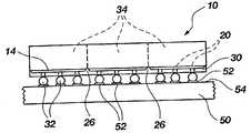
- FIG. 4An example of such a configuration is depicted in FIG. 4, wherein carrier substrate 50 is provided.
- external conductive elements 32are patterned in such a way as to conform to a similar pattern of terminal pads 52 on carrier substrate 50 .
- Carrier substrate 50may be any type of substrate such as, for example, a printed circuit board made from fiberglass resin (i.e., FR-4, FR-5, etc.) or other carrier substrates used and known to those skilled in the art.
- the physical connectionallows a block of devices to be attached to carrier substrate 50 with high precision and in a single step, rather than discretely attaching each semiconductor device 34 using conventional, single-die flip-chip aligner/bonder equipment. Additionally, the close mutual proximity of each semiconductor device 34 provides for a greater circuit density on carrier substrate 50 than would otherwise be provided using the singulated semiconductor device approach of prior systems. Overall operational speed of the assembly will improve because of the closer mutual physical proximity of the semiconductor devices 34 . As previously alluded to, complete modules can be fabricated, such as, for example, memory modules, where four, six, eight, or other plurality of semiconductor devices 34 can be readily assembled with a carrier substrate 50 in a single step, resulting in a smaller package with increased performance than otherwise possible with singulated semiconductor devices 34 .
- FIG. 5is a cross-sectional view of several alternative cross-sectional configurations for the channels or troughs 26 .
- channels or troughs 26need not be actual mechanically-effectuated cuts but may be formed as previously mentioned, using either laser beams or dry plasma etching to achieve the flat-bottomed, parallel side wall shape of channels or troughs 56 or isotropic wet chemical etching to achieve the rounded-bottom, parallel shape of channels or troughs 58 .
- FIG. 6depicts a top plan view of a semiconductor wafer 60 that is populated with a plurality of semiconductor devices 34 .
- a plurality of external conductive elements 32resides on the active surface 14 of each semiconductor device 34 .
- External conductive elements 32may be, for example, solder bond balls, conductive columns, or other similar conductive elements that may be utilized for surface mount connection on a carrier substrate.
- intermediate conductive elements 20may, for example, be used without further processing and in the form of a land grid array to connect to a carrier substrate having conductive elements projecting therefrom.
- external conductive elements in the form of bond padsmay be formed over the ends of intermediate conductive elements to enlarge the connection areas to mate with the carrier substrate bumps.
- an anisotropically conductive filmmay be applied to each semiconductor device site to connect between the intermediate conductive elements and a carrier substrate. Further shown are channels or troughs 26 that crisscross the surface of semiconductor wafer 60 in the manner previously described, so as to isolate each semiconductor device 34 from one another.
- a substrate 10may be provided with intermediate conductive elements 20 or 40 over active surface 14 as described above, after which active surface 14 is covered with encapsulant material 30 and then planarized to expose intermediate conductive elements 20 or 40 .
- a layer of metal compatible with the intermediate conductive elements 20 or 40is formed over the planarized surface of encapsulant material 30 and covered with a photoresist which is patterened to known in the art to form circuit traces 70 extending from intermediate conductive elements 20 or 40 to a position over, and preferably to or across the centers of, channels or troughs 26 .
- a row of trace ends 72may be employed as edge contacts to connect a vertically oriented device 34 in a plug-in type direct chip attach (DCA) configuration to edge connectors 82 along one side of a slot 84 in a carrier substrate 80 , as illustrated in FIG. 7B.
- DCAdirect chip attach
- FIG. 8depicts a computer system 100 that includes an input device 102 and an output device 104 .
- Computer 100further comprises a microprocessor 106 that is coupled to the input device 102 and the output device 104 via a direct connection or a computer bus 108 , as shown.
- Microprocessor 106may be formed in such a manner as to utilize the attachment and packaging structures of the present invention.
- a memory device 110 according to the present invention(which comprises a multi-chip memory module) further connects to microprocess 106 via computer bus 108 .
- Memory device 110may comprise one or more semiconductor devices 34 (either as a partial substrate or as completely singulated dice) or even a complete substrate 10 as mounted on a carrier substrate according to the present invention.
Landscapes
- Engineering & Computer Science (AREA)
- Microelectronics & Electronic Packaging (AREA)
- Computer Hardware Design (AREA)
- Power Engineering (AREA)
- Physics & Mathematics (AREA)
- Condensed Matter Physics & Semiconductors (AREA)
- General Physics & Mathematics (AREA)
- Manufacturing & Machinery (AREA)
- Wire Bonding (AREA)
- Dicing (AREA)
- Encapsulation Of And Coatings For Semiconductor Or Solid State Devices (AREA)
Abstract
Description
- This application is a divisional of application Ser. No. 09/917,127 filed Jul. 27, 2001, pending, which is a divisional of application Ser. No. 09/586,243, filed Jun. 2, 2000, pending.[0001]
- 1. Field of the Invention[0002]
- The present invention relates to semiconductor devices and methods for fabricating semiconductor devices. More specifically, the invention relates to a method for packaging a semiconductor die having conductive elements that protrude at least to the surface of a covering or encapsulation of the die active surface.[0003]
- 2. State of the Art[0004]
- In semiconductor manufacture, a single semiconductor die or chip including a plurality of integrated circuits on an active surface thereof is typically mounted within a sealed package of a silicon-filled epoxy formed thereabout by a process known as transfer-molding. The package generally protects the die from physical damage and from contaminants, such as moisture or chemicals, found in the surrounding environment. The package also provides a lead system for connecting the electrical devices (integrated circuits) formed on the die to a printed circuit board or other higher-level packaging.[0005]
- Packaged semiconductor dice containing integrated circuits for a broad range of purposes are currently mass produced. Even slight savings in the cost of packaging one such semiconductor die circuit can generate significant overall cost savings to the manufacturer, due to large production volumes, if the reduced-cost packaging affords required package integrity. Further, reduction in package size can eliminate size-based restrictions for use of a die on ever more crowded carrier substrates such as printed circuit boards (PCBs), where available “real estate” is at a premium. Therefore, continual cost reductions and quality improvements in the manufacture of these semiconductor packages, while maintaining the overall lateral dimensions of such packages at a reduced size, are of great value in the semiconductor manufacturing field.[0006]
- In many semiconductor applications, formation of conductive bumps or other external conductive elements on the bond pads of a die is desirable, if not necessary, to connect the die to external conductors. The most common applications where conductive bumps or other elements are used include tape automated bonding (TAB), flip-chip attachment of a die to a carrier substrate, and direct chip attachment (DCA) of a die to a carrier substrate. Conductive bumps may comprise metals or alloys including, without limitation, conventional tin\lead solders, or may comprise conductive or conductor-filled epoxies, all as known in the art. Formation of the conductive bumps used in these applications can be accomplished using a variety of commonly known methods, such as deposition onto bond pads by screening or printing, preform ball or bump placement, or ball bumping using wire bonding equipment to form each individual bump in situ.[0007]
- A widely practiced way to increase the number of available input/output (I/O) connections for a die is to use flip-chip methodology for packaging, where an array of conductive elements (e.g., conductive bumps, ball bonds, conductive pillars or other conductive structures) is positioned on the active surface or circuit face of the die, which is then mounted active surface down upon a single chip or multi-chip module carrier substrate.[0008]
- Because of relatively high manufacturing costs associated with state-of-the-art metal deposition equipment dedicated specifically to bumping a die for flip-chip attachment, some semiconductor manufacturers have resorted to the aforementioned ball bumping using conventional wire bonding tools (capillaries) to form conductive bumps over the bond pads. In the ball bumping process, a capillary of the wire bonding tool carries a conductive wire toward a bond pad on which a bump is to be formed. A ball is formed at an end of the wire by heating and melting the metal wire. The wire bonding tool capillary then presses the ball against the planar bond pad and the portion of the wire extending past the ball is cut, leaving a ball bump on the bond pad.[0009]
- A flip-chip or bumped (raised) die is a semiconductor chip (die) having bumps formed on bond pads on the active surface or front side of the die, the bumps being used as electrical and mechanical connectors to conductors of higher level packaging, such as a PCB or other carrier substrate. The bumped die is inverted (flipped) and bonded to trace ends or other terminals on a carrier substrate by means of the bumps. As noted above, diverse materials are conventionally used to form the bumps on the die, such as solder, conductive polymers, and conductor-filled polymers. Typically, if the bumps are solder bumps, solder segments are deposited on the die and then reflowed to form a substantially spherical shape, and subsequently reheated to form a solder joint between the bond pads on the so-called flip-chip and terminal pads on the carrier substrate, the solder joint providing both electrical and mechanical connections between the flip-chip and substrate.[0010]
- Conventional flip-chip IC devices formed according to the aforementioned fabrication processes exhibit a number of shortcomings. For example, since the active surface of the chip is relatively unprotected, being covered only with a thin passivation layer, damage to the chip can occur during attachment of the chip to the carrier substrate. Likewise, such damage to the chip can occur during handling of the chip or while conducting reliability testing of the same. Moreover, directly bumping the relatively delicate bond pads, even with one or more layers of under-bump metallization thereover to facilitate metallurgical compatibility between the bond pad and the metal bump, may itself cause damage.[0011]
- As disclosed in U.S. Pat. No. 5,496,775 to Brooks, encapsulated IC dice having contact bumps have been developed in an attempt to solve some of these problems. In the fabrication process of Brooks, gold balls, which function as leads or contacts, are welded in a stacked or tower fashion onto each bond pad of the IC die. The gold ball tower-bonded die is then placed into a mold and onto a first layer of encapsulation material contained therein. A second layer of encapsulation material is then applied over the tower side of the die, which completely covers the die surface, partially submerging the towers in the encapsulant. The encapsulated IC die is removed from the mold and mounted to tab tape or a PCB, with the nonsubmerged portions of the towers providing an electrical connection thereto. Although these semiconductor packages have solved a number of problems, the fabrication process to form such packages requires numerous fabrication steps and specialized equipment and materials, especially for the creation of the ball towers and the related steps providing encapsulation around the towers. Also, the required formation of stacks of multiple gold balls in the package inevitably increases the vertical size or height of the package.[0012]
- In view of the foregoing limitations, there is a need in the semiconductor art for an improved method for forming semiconductor packages of compact size (“chip scale packages” or “CSPs”) approximating the length and width of the die itself and having a minimal number of component parts. Specifically, there is a need for an improved method for forming chip scale packages that have a uniform encapsulant extending from edge to edge of the active surface to provide a substantially hermetic seal across the entire active surface and over exposed edges of the layer or layers of integrated circuitry formed thereon. There is a further need for an improved method for forming a chip scale package that does not significantly complicate the manufacturing or handling of the integrated circuitry and that is repeatable and reliable when using conventional mass production manufacturing techniques. Preferably, the chip scale package could be substantially formed during and simultaneously with the fabrication of the die itself in wafer form.[0013]
- The present invention includes a method of forming a semiconductor device by forming or providing a semiconductor wafer having an active surface defining a large plurality of individual die locations thereon. As used herein, the term “wafer” includes traditional wafer structures as well as silicon-on-insulator (SOI), silicon-on-glass (SOG) and silicon-on-sapphire (SOS) substrates, among other semiconductor substrates known in the art. The active surface of the semiconductor wafer includes bond pads thereon for making external electrical connections. Either the bond pads are provided with intermediate conductive elements thereon or the input/output connections provided by the bond pads are redistributed into a different pattern or array using traces over the active surface, and the intermediate conductive elements formed at the redistributed input/output locations. A grid of channels or troughs is formed, as by scribing with a wafer saw or etching, between die locations and of sufficient depth to pass through the active surface to an insulative region to isolate individual, adjacent die active surface regions on the semiconductor wafer. A flowable material used to encapsulate at least the active surface of the entire semiconductor wafer is applied thereto to cover the intermediate conductive elements and is then planarized to expose the intermediate conductive elements. The flowable encapsulant material extends into the channel regions, sealing the exposed, lateral edges of the active surface surrounding each individual die location. The intermediate conductive elements are then provided with external conductive elements projecting transversely from the surface of the encapsulant layer, or an anisotropically-conductive (so-called “Z-axis”) film may be placed over the substrate. Alternatively, conductive traces may be formed to extend between the exposed ends of the intermediate conductive elements and one or more edges of each die location to form one or more rows of edge connects suitable for DCA to a carrier substrate. The semiconductor wafer is cut through its entire depth, as with a wafer saw, along the centers of the channel regions to separate, or “singulate,” the individual die locations into flip-chip or DCA dice to be individually connected to a carrier substrate. Alternatively, the entire semiconductor substrate or a group of unsingulated dice may be mated to a carrier substrate and bonded thereto using the external conductive elements. As yet another alternative, the exposed ends of intermediate conductive elements alone may be employed as a land grid array for attachment of a die, substrate segment or entire semiconductor substrate to a bumped carrier substrate, and may optionally be provided with larger conductive pads thereover to facilitate connection to the carrier substrate bumps. As still another alternative, conductive traces can be extended from the bond pads across the active surface and down channel side walls between at least some of the individual die locations prior to encapsulation of the active surface of the semiconductor substrate, the trace ends then being exposed during singulation of the dice to form rows of electrical contacts along edges of the singulated dice, or groups of dice which remain together.[0014]
- While the specification concludes with claims particularly pointing out and distinctly claiming that which is regarded as the present invention, the advantages of this invention can be more readily ascertained from the following description of the invention when read in conjunction with the accompanying drawings in which:[0015]
- FIGS.[0016]1A-1F illustrate cross-sectional views of the process steps used in carrying out the method of the present invention;
- FIG. 2 depicts a singulated die with an active surface conformally covered by an encapsulant material;[0017]
- FIG. 3 illustrates a cross-sectional view of an alternative structural embodiment of the invention;[0018]
- FIG. 4 depicts a group of unsingulated semiconductor devices applied to a carrier substrate;[0019]
- FIG. 5 depicts alternative cross-sectional shapes of channels or troughs between die locations;[0020]
- FIG. 6 depicts a top plan view of a plurality of dice laid out on a semiconductor wafer where the channels or troughs have been formed along streets between individual die locations;[0021]
- FIGS. 7A and 7B, respectively, depict a portion of a semiconductor substrate having two adjacent dice with traces extending over a channel or trough therebetween to provide a DCA configuration upon singulation and a singulated die in a DCA configuration with a carrier substrate; and[0022]
- FIG. 8 depicts a computer system incorporating a microprocessor or a memory device, or both, which incorporates a chip scale package manufactured according to the present invention.[0023]
- A fabrication process of the invention is depicted in FIGS.[0024]1A-1F, which figures include a
semiconductor substrate 10 having a plurality ofbond pads 12 on anactive surface 14 thereof, bearing at least one layer16 of integrated circuitry18 thereon. For purposes of simplicity, elements common to FIGS.1A-1F will hereinafter be numbered identically in subsequent figures illustrating other preferred methods according to the present invention. - [0025]
Semiconductor substrate 10 may comprise a wafer, as defined above, including a plurality of individual die locations thereon. Thebond pads 12 are “bumped” with intermediateconductive elements 20 which project upwardly fromactive surface 14, or some or all of the input\output locations for each die are redistributed using conductive traces prior to being bumped, such processes being well known in the art. If the external conductive elements (see below) are metallurgically incompatible withbond pads 12, the intermediateconductive elements 20 may be of a layer or layers of metals which will provide a better metallurgical bond therebetween. One such example, in the case of Al bond pads and tin/lead solder external conductive elements, would be to form intermediateconductive elements 20 of three superimposed layers (top to bottom) of copper, copper/chromium alloy, and chromium. It is also contemplated that thebond pads 12 may be bumped using a wire bonding capillary, or with solder of a higher melting temperature than that of another solder to be employed in externalconductive elements 32, as referenced below. Intermediateconductive elements 20 may also comprise a conductive or conductor-filled epoxy, such as a silver-filled epoxy. The only significant constraints on the material and configuration selected for intermediateconductive elements 20 are compatibility with thebond pads 12 or other input/output contacts onsubstrate 10 as well as with externalconductive elements 32, and sufficient temperature tolerance and physical strength to withstand encapsulation ofactive surface 14 ofsubstrate 10 and formation of externalconductive elements 32 thereon. - A preferred[0026]
semiconductor substrate 10 has a standardized number of bond pads or other input/output locations 12 for every die location (the term “bond pad” as used herein also encompassing redistributed input/output locations), thebond pads 12 being located in arrays, one array for each die location, withbond pads 12 laterally spaced from one another at, for example, a uniform pitch. The arrays are positioned at specific locations relative to a reference point (not shown) of thesemiconductor substrate 10, in order to facilitate precise relative positioning ofsemiconductor substrate 10 and processing equipment therefor. This reference point may include the side edge ofsemiconductor substrate 10 or a center line of substrate10 (not shown). Alternatively, the number, pitch and array configuration ofbond pads 12 may be nonstandardized, for example, if different input/output arrangements are desired for dice formed on thesame substrate 10. - After the formation of[0027]
bond pads 12, FIG. 1B depicts how a plurality of channels ortroughs 26 is formed on theactive surface 14 ofsemiconductor substrate 10 to define individual die locations onsubstrate 10. As used herein, the term “individual dice” specifically includes, without limitation, partial wafers bearing more than one die as well as single dice. Channels ortroughs 26 extend at a depth sufficient enough to pass entirely through the at least one layer16 of integrated circuitry18 upon theactive surface 14 ofsubstrate 10 and are cut in a grid pattern comprising a first group of mutually parallel channels ortroughs 26 which are arranged perpendicular to a second group of mutually parallel channels ortroughs 26. The channels ortroughs 26 are located to extend along the so-called “streets” between individual semiconductor die locations onsubstrate 10, wherein neither active or passive components of integrated circuitry18, or interconnect structures for same, are typically located. Various types of methods may be utilized to form channels ortroughs 26 having different cross-sectional configurations. For example, a beveled or chamfered channel as shown may be formed using a wafer saw blade or an isotropic etch. A laser drill may be used to form a parallel-sided channel, while an etching process, such as dry or plasma etching or wet solution etching, may be used to form channels with either substantially parallel sides or sloped sides, depending upon the anisotropic or isotropic tendencies of the etch employed. Each one of these types of cutting has advantages and disadvantages over the other types and it will be readily apparent to those skilled in the art which applications would be best used under particular circumstances. For example, where deep channels are preferred or required, wafer saw scribing is preferable as it is rapid and accurate. Where small-dimensioned channels with tolerances that must be tightly controlled are preferred or required, dry or wet etches would be utilized. - After the formation of channels or[0028]
troughs 26, aflowable encapsulant material 30 may be placed across the entire surface ofsemiconductor substrate 10 to such a depth as to entirely cover intermediateconductive elements 20, the encapsulant material also filling channels ortroughs 26. This is depicted in FIG. 1C. One preferred method of applyingencapsulant material 30 toactive surface 14 ofsubstrate 10 is the previously mentioned transfer molding, wherein a mold having a cavity configured to receivesubstrate 10 with a void aboveactive surface 14 of a depth or height at least as great as the height of intermediateconductive elements 20 is injected with a molten, silicon particle-filled epoxy. Transfer-molding is typically only effected on a plurality of singulated dice secured to a lead frame strip, with each die residing in an individual cavity having lead fingers of an associated lead frame extending therefrom, the lead fingers subsequently being severed from the lead frame strip and bent to a final configuration in a so-called “trim and form” operation. Hence, the transfer molding of an entire semiconductor substrate such as a wafer is also believed to be novel and to comprise part of the present invention. Onceencapsulant material 30 has been sufficiently cured to a substantially rigid state, the surface ofencapsulant material 30 is abrasively planarized, as by so-called chemical-mechanical planarization (CMP) down to a level to expose the tops of intermediateconductive elements 20, as shown in FIG. 1D.Encapsulant material 30 may also comprise an epoxy compound molded in an open or closed mold cavity over theactive surface 14 ofsubstrate 10, or may be selected from a dispensed epoxy or polyimide as well known to those skilled in the art for encapsulation or sealing of semiconductor dice. Suitable materials for use as an encapsulant material preferably exhibit low moisture permeability, nonconductivity (i.e., having low ionic contamination), good thermal conductivity, high physical resilience, and a low coefficient of thermal expansion (CTE). Preferred materials include polymers as a general class and, specifically, filled polymers, epoxies, silicones, silicone-carbon resins, polyimides and polyurethanes, as well as glasses. It should be again noted that the filling of channels ortroughs 26 withencapsulant material 30 results in the substantially hermetic sealing of exposed peripheral edges of the at least one layer16 of integrated circuitry18 on theactive surface 14. - Next, as shown in FIG. 1E, external conductive elements designated generally as[0029]32 are formed or placed on each intermediate
conductive element 20. External conductive elements may, for example, comprise segments of solder paste stenciled or screen printed onto intermediateconductive elements 20, preformed solder balls, conductive or conductor-filled epoxies, or anisotropically conductive films or segments of such films. - If solder is employed in paste form (rather than as preformed, already-reflowed balls), a proper amount of solder paste per segment should be used to adequately cover the intermediate[0030]
conductive elements 20, to remain tacky without slumping, and to create a ball having sufficient size for the intended application when the solder paste is reflowed. Suitable solder pastes for use with the instant process can comprise any combination of chemical components that produces paste properties resulting in the desired chemical and physical characteristics for application (e.g., bonding characteristics and viscosity), reflow, cleaning, and formation of the final, encapsulated, raised ball-bond semiconductor structure. For example, the selected solder paste should be able to substantially retain the original printed or dot-dispensed pattern at room temperature and during reflow. Because the spacing or pitch between bond pads is continually decreasing in the art, adequate control of slump is increasingly critical to the prevention of bridging and shorting between bond pads. Likewise, the solder paste should, when reflowed as described hereafter, uniformly coalesce to a substantially spherical ball that is substantially free of surrounding small satellite balls. Preferably, the solder paste is a low-melting-point alloy, usually of lead (Pb) and tin (Sn), that can wet copper, conduct current, and mechanically join conductors and the like. Other suitable ingredients for use as a solder paste include, without limitation, aluminum, palladium, gold, copper, indium, silver, tin, lead and combinations or alloys thereof. The solder paste may conventionally include a blend of the desired weight percent of alloy powder into a flux to produce a homogeneous product. The viscosity of the solder paste should be adjusted, if necessary, to prevent problems such as spattering, excessive slump, overly rapid drying on the stencil screen and accompanying loss of tack, clogging of stencil apertures, stringing, smearing, inadequate solder deposition, and nonwetting. Use of solder pastes containing solvent-soluble and water-soluble ingredients is preferred since these ingredients substantially evaporate during the reflow process, thus leaving a minimal residue that is, by formulation, removable with either water or solvent. - Once solder paste has been applied to[0031]
bond pads 12, the solder paste is reflowed to form external conductive elements in the form of substantiallyspherical balls 32, as illustrated in FIG. 1E. The solder paste can be melted by any suitable means, such as electrical resistance or hot gas heating, forced air oven, radiant heating, liquid immersion, vapor phase condensation methods, or by any method of reflowing known in the art. Temperatures used to accomplish the reflowing of the solder paste are necessarily dependent on the composition of the solder paste being used. Heating times and temperatures must, therefore, be closely controlled to prevent melting or decomposition of thesemiconductor substrate 10, including the substructures thereon (e.g., intermediateconductive elements 20,bond pads 12 and the underlying integrated circuitry18). With these variables in mind, an appropriate solder paste must be selected for use in conjunction with a selected semiconductor substrate. - It is noted that any size of[0032]
ball 32 may be formed so long as the dimensions of the ball comply with design constraints of the final semiconductor device. For most applications,balls 32 may have a diameter of from about 5 mil to about 15 mil. Because larger and smaller ball bond dimensions are envisioned for a variety of structures, other sized balls may be similarly manufactured. - Once the[0033]
solder balls 32 have been formed on theirrespective bond pads 12,semiconductor substrate 10 is diced into discrete semiconductor devices such assingulated dice 34 as depicted in FIG. 1F. The dicing ofsemiconductor devices 34 may be performed by a wafer saw, as known in the art. Once thesemiconductor devices 34 are diced, they may be applied to a carrier substrate (not shown) in a conventional, flip-chip attachment scheme. - There are several methods of attaching the completed bumped die onto a carrier substrate, such as a PCB. For example, it is possible to reflow the balls to the carrier substrate for a permanent connection, or to mechanically bias the balls on the active surface of the die into receptacle- or socket-type terminals on the carrier substrate so as to provide for easier removal and replacement.[0034]
- FIG. 2 depicts how[0035]
encapsulant material 30 may be applied to both theactive surface 14 and theback side 22 ofsemiconductor substrate 10 in a substantially conformal manner so as to fill in channels ortroughs 26, but not to overfill same to the point of being level with the top surfaces of intermediateconductive elements 20. The depressions29 (shown in FIGS.1B-1D by broken lines) of theencapsulant material 30 over channels ortroughs 26 are useful in that during the dicing operation, the recessed portions ofencapsulant material 30 over channels ortroughs 26 provide alignment guidance for the dicing of thesubstrate 10 intodiscrete semiconductor devices 34. Again, channels ortroughs 26 extend below the layer16 of integrated circuitry18 onactive surface 14 ofsemiconductor substrate 10. As is shown, thesubstrate 10 has been singulated intodiscrete semiconductor devices 34. The sloped sidewalls of theencapsulant material 30 extend past the edges of layer16 exposed by, for example, scribing with a wafer saw in such a manner as to provide a substantially hermetic seal against water, dust, and other contaminants that might otherwise damage or otherwise compromise the integrity and operation ofsemiconductor device 34. The intermediateconductive elements 20, if not completely covered but only partially covered but supported at their peripheries byencapsulant material 30 as shown in broken line at36, may in fact be used for connection to higher-level packaging without further disposition of externalconductive elements 32 thereon and also without planarization, except to an extent necessary to ensure good exposure of the conductive materials of intermediateconductive elements 20. If completely covered, the upper ends of intermediateconductive elements 20 may be exposed by abrasive planarization, or theencapsulant material 30 selectively etched to expose the upper ends. - Another embodiment of the invention is depicted in FIG. 3. The fabrication process is initiated by applying a conductive elastomer material, such as a metal-filled rubber or silicone compound, onto[0036]
bond pads 12 to form an intermediateconductive element 40. A proper amount of conductive elastomer material must be used to adequately coverbond pads 12 and to create an intermediateconductive element 40 of sufficient size when the same is reshaped, as described below. The conductive elastomer material can be applied by any suitable means known in the art such as extrusion or stenciling. After the formation of intermediateconductive elements 40, theencapsulant material 30 is applied across theactive surface 14 in such a manner as to fill in all channels ortroughs 26 and extend over the tops of intermediateconductive elements 40. Next, a planarization step is performed that levels theencapsulant material 30 to the tops of intermediateconductive elements 40. Subsequently, asecond bond pad 42 may be optionally formed on top of intermediateconductive elements 40 and an optional external conductive element32 (shown as a conductive pillar) may then be attached using conventional methods tosecond bond pad 42. - As an alternative approach to the above, the[0037]
encapsulant material 30 may be applied across theactive surface 14 ofsemiconductor substrate 10 in such a manner as to cover thebond pads 12. Theencapsulant material 30, in the form of a photosensitive polymer, may be applied in a conventional manner to theactive surface 14 of thesemiconductor substrate 10 and patterned using a mask to create openings therethrough over thebond pads 12, after which the bond pad openings may be filled with a suitable material to form intermediateconductive elements 40. Then, thesemiconductor devices 34 are singulated fromsubstrate 10 along the separation lines46 (dashed lines) down the center lines of channels ortroughs 26. - Intermediate[0038]
conductive elements 40 may be formed in any variety of suitable shapes and sizes so long as the dimensions of the bumps comply with design constraints of the final semiconductor device assembly. For most applications, intermediateconductive elements 40 will preferably be cylindrical or pillar-shaped. However, as a further alternative and as shown in broken lines in FIG. 3, intermediateconductive elements 40 may comprisetraces 40twhich are formed onactive surface 14 to extend frombond pads 12 to a peripheral edge of adevice 34, and at least toseparation line 46. Thus, whendevice 34 is severed fromsubstrate 10, the ends40eoftraces 40tare exposed and may be used to abut and contact a row of connectors at the bottom of a slot of a carrier substrate in a DCA configuration. - Rather than singulate each and every[0039]
semiconductor device 34 as shown in FIGS. 1F and 3, a block ofsemiconductor devices 34 can remain unsingulated in order to facilitate unitary attachment of the block to a carrier substrate. In such a manner, for example, a plurality of memory dice may be attached as a group (i.e., partial wafer or other semiconductor substrate) to a carrier substrate to form a multi-chip module. An example of such a configuration is depicted in FIG. 4, whereincarrier substrate 50 is provided. For eachsemiconductor device 34, externalconductive elements 32 are patterned in such a way as to conform to a similar pattern ofterminal pads 52 oncarrier substrate 50.Carrier substrate 50 may be any type of substrate such as, for example, a printed circuit board made from fiberglass resin (i.e., FR-4, FR-5, etc.) or other carrier substrates used and known to those skilled in the art. Once thesemiconductor substrate 10 is positioned such that externalconductive elements 32 align with theterminal pads 52 on thesurface 54 ofcarrier substrate 50, the entire assembly may be heated to such a temperature as to cause the external conductive elements (if solder) to reflow and metallurgically attach to theterminal pads 52. With channels ortroughs 26 extending through theactive surface 14 ofsubstrate 10, eachsemiconductor device 34 is isolated from one another electrically, but not physically. The physical connection allows a block of devices to be attached tocarrier substrate 50 with high precision and in a single step, rather than discretely attaching eachsemiconductor device 34 using conventional, single-die flip-chip aligner/bonder equipment. Additionally, the close mutual proximity of eachsemiconductor device 34 provides for a greater circuit density oncarrier substrate 50 than would otherwise be provided using the singulated semiconductor device approach of prior systems. Overall operational speed of the assembly will improve because of the closer mutual physical proximity of thesemiconductor devices 34. As previously alluded to, complete modules can be fabricated, such as, for example, memory modules, where four, six, eight, or other plurality ofsemiconductor devices 34 can be readily assembled with acarrier substrate 50 in a single step, resulting in a smaller package with increased performance than otherwise possible withsingulated semiconductor devices 34. - FIG. 5 is a cross-sectional view of several alternative cross-sectional configurations for the channels or[0040]
troughs 26. In this example, channels ortroughs 26 need not be actual mechanically-effectuated cuts but may be formed as previously mentioned, using either laser beams or dry plasma etching to achieve the flat-bottomed, parallel side wall shape of channels ortroughs 56 or isotropic wet chemical etching to achieve the rounded-bottom, parallel shape of channels ortroughs 58. - FIG. 6 depicts a top plan view of a[0041]
semiconductor wafer 60 that is populated with a plurality ofsemiconductor devices 34. A plurality of externalconductive elements 32 resides on theactive surface 14 of eachsemiconductor device 34. Externalconductive elements 32 may be, for example, solder bond balls, conductive columns, or other similar conductive elements that may be utilized for surface mount connection on a carrier substrate. It should also be appreciated that intermediateconductive elements 20 may, for example, be used without further processing and in the form of a land grid array to connect to a carrier substrate having conductive elements projecting therefrom. Optionally, external conductive elements in the form of bond pads may be formed over the ends of intermediate conductive elements to enlarge the connection areas to mate with the carrier substrate bumps. As a further option, an anisotropically conductive film may be applied to each semiconductor device site to connect between the intermediate conductive elements and a carrier substrate. Further shown are channels ortroughs 26 that crisscross the surface ofsemiconductor wafer 60 in the manner previously described, so as to isolate eachsemiconductor device 34 from one another. - As a further alternative in accordance with the invention and as depicted in FIG. 7A, a[0042]
substrate 10 may be provided with intermediateconductive elements active surface 14 as described above, after whichactive surface 14 is covered withencapsulant material 30 and then planarized to expose intermediateconductive elements conductive elements encapsulant material 30 and covered with a photoresist which is patterened to known in the art to form circuit traces70 extending from intermediateconductive elements troughs 26. Then,semiconductor devices 34 are singulated along the centers of channels ortroughs 26, a row of trace ends72 may be employed as edge contacts to connect a vertically orienteddevice 34 in a plug-in type direct chip attach (DCA) configuration toedge connectors 82 along one side of aslot 84 in acarrier substrate 80, as illustrated in FIG. 7B. - FIG. 8 depicts a[0043]
computer system 100 that includes aninput device 102 and anoutput device 104.Computer 100 further comprises amicroprocessor 106 that is coupled to theinput device 102 and theoutput device 104 via a direct connection or acomputer bus 108, as shown.Microprocessor 106 may be formed in such a manner as to utilize the attachment and packaging structures of the present invention. Additionally, amemory device 110 according to the present invention (which comprises a multi-chip memory module) further connects to microprocess106 viacomputer bus 108.Memory device 110 may comprise one or more semiconductor devices34 (either as a partial substrate or as completely singulated dice) or even acomplete substrate 10 as mounted on a carrier substrate according to the present invention. - Although the preferred embodiments of the present invention have been disclosed for illustrative purposes, those skilled in the art will appreciate that various modifications, additions, and substitutions are possible without departing from the scope and spirit of the invention as disclosed in the accompanying claims.[0044]
Claims (6)
Priority Applications (3)
| Application Number | Priority Date | Filing Date | Title |
|---|---|---|---|
| US10/624,833US6900079B2 (en) | 2000-06-02 | 2003-07-22 | Method for fabricating a chip scale package using wafer level processing |
| US11/057,921US7183191B2 (en) | 2000-06-02 | 2005-02-15 | Method for fabricating a chip scale package using wafer level processing |
| US11/711,420US7727858B2 (en) | 2000-06-02 | 2007-02-26 | Method for fabricating a chip scale package using wafer level processing |
Applications Claiming Priority (3)
| Application Number | Priority Date | Filing Date | Title |
|---|---|---|---|
| US09/586,243US6717245B1 (en) | 2000-06-02 | 2000-06-02 | Chip scale packages performed by wafer level processing |
| US09/917,127US6780746B2 (en) | 2000-06-02 | 2001-07-27 | Method for fabricating a chip scale package using wafer level processing and devices resulting therefrom |
| US10/624,833US6900079B2 (en) | 2000-06-02 | 2003-07-22 | Method for fabricating a chip scale package using wafer level processing |
Related Parent Applications (1)
| Application Number | Title | Priority Date | Filing Date |
|---|---|---|---|
| US09/917,127DivisionUS6780746B2 (en) | 2000-06-02 | 2001-07-27 | Method for fabricating a chip scale package using wafer level processing and devices resulting therefrom |
Related Child Applications (1)
| Application Number | Title | Priority Date | Filing Date |
|---|---|---|---|
| US11/057,921DivisionUS7183191B2 (en) | 2000-06-02 | 2005-02-15 | Method for fabricating a chip scale package using wafer level processing |
Publications (2)
| Publication Number | Publication Date |
|---|---|
| US20040126928A1true US20040126928A1 (en) | 2004-07-01 |
| US6900079B2 US6900079B2 (en) | 2005-05-31 |
Family
ID=24344920
Family Applications (5)
| Application Number | Title | Priority Date | Filing Date |
|---|---|---|---|
| US09/586,243Expired - LifetimeUS6717245B1 (en) | 2000-06-02 | 2000-06-02 | Chip scale packages performed by wafer level processing |
| US09/917,127Expired - Fee RelatedUS6780746B2 (en) | 2000-06-02 | 2001-07-27 | Method for fabricating a chip scale package using wafer level processing and devices resulting therefrom |
| US10/624,833Expired - LifetimeUS6900079B2 (en) | 2000-06-02 | 2003-07-22 | Method for fabricating a chip scale package using wafer level processing |
| US11/057,921Expired - LifetimeUS7183191B2 (en) | 2000-06-02 | 2005-02-15 | Method for fabricating a chip scale package using wafer level processing |
| US11/711,420Expired - Fee RelatedUS7727858B2 (en) | 2000-06-02 | 2007-02-26 | Method for fabricating a chip scale package using wafer level processing |
Family Applications Before (2)
| Application Number | Title | Priority Date | Filing Date |
|---|---|---|---|
| US09/586,243Expired - LifetimeUS6717245B1 (en) | 2000-06-02 | 2000-06-02 | Chip scale packages performed by wafer level processing |
| US09/917,127Expired - Fee RelatedUS6780746B2 (en) | 2000-06-02 | 2001-07-27 | Method for fabricating a chip scale package using wafer level processing and devices resulting therefrom |
Family Applications After (2)
| Application Number | Title | Priority Date | Filing Date |
|---|---|---|---|
| US11/057,921Expired - LifetimeUS7183191B2 (en) | 2000-06-02 | 2005-02-15 | Method for fabricating a chip scale package using wafer level processing |
| US11/711,420Expired - Fee RelatedUS7727858B2 (en) | 2000-06-02 | 2007-02-26 | Method for fabricating a chip scale package using wafer level processing |
Country Status (1)
| Country | Link |
|---|---|
| US (5) | US6717245B1 (en) |
Cited By (9)
| Publication number | Priority date | Publication date | Assignee | Title |
|---|---|---|---|---|
| US20040129451A1 (en)* | 2001-07-27 | 2004-07-08 | Wachtler Kurt P. | Method of separating semiconductor dies from a wafer |
| US20050164486A1 (en)* | 2003-07-22 | 2005-07-28 | Lua Edmund K.T. | Semiconductor substrates including I/O redistribution using wire bonds and anisotropically conductive film, methods of fabrication and assemblies including same |
| US20050214975A1 (en)* | 2004-03-26 | 2005-09-29 | Denny Chao | Method of fabricating the planar encapsulated surface |
| US20070045806A1 (en)* | 2004-02-05 | 2007-03-01 | United Microelectronics Corp. | Structure of an ultra-thin wafer level stack package |
| US20080284000A1 (en)* | 2007-05-17 | 2008-11-20 | Micron Technology, Inc. | Integrated Circuit Packages, Methods of Forming Integrated Circuit Packages, And Methods of Assembling Integrated Circuit Packages |
| US20090302468A1 (en)* | 2008-06-05 | 2009-12-10 | Samsung Electro-Mechanics Co., Ltd. | Printed circuit board comprising semiconductor chip and method of manufacturing the same |
| US20110243176A1 (en)* | 2010-03-31 | 2011-10-06 | Seagate Technology Llc | Integrating and aligning laser chips on sliders for hamr applications |
| US20130313719A1 (en)* | 2012-05-25 | 2013-11-28 | Infineon Technologies Ag | Chip packages and methods for manufacturing a chip package |
| US20230062701A1 (en)* | 2021-08-24 | 2023-03-02 | Micron Technology, Inc. | Semiconductor assemblies with system and methods for aligning dies using registration marks |
Families Citing this family (199)
| Publication number | Priority date | Publication date | Assignee | Title |
|---|---|---|---|---|
| US7157314B2 (en) | 1998-11-16 | 2007-01-02 | Sandisk Corporation | Vertically stacked field programmable nonvolatile memory and method of fabrication |
| US6352881B1 (en) | 1999-07-22 | 2002-03-05 | National Semiconductor Corporation | Method and apparatus for forming an underfill adhesive layer |
| JP2001102486A (en)* | 1999-07-28 | 2001-04-13 | Seiko Epson Corp | Semiconductor device substrate, semiconductor chip mounting substrate, semiconductor device and its manufacturing method, circuit board, and electronic equipment |
| US6350664B1 (en)* | 1999-09-02 | 2002-02-26 | Matsushita Electric Industrial Co., Ltd. | Semiconductor device and method of manufacturing the same |
| JP4120133B2 (en)* | 2000-04-28 | 2008-07-16 | 沖電気工業株式会社 | Semiconductor device and manufacturing method thereof |
| US8575719B2 (en) | 2000-04-28 | 2013-11-05 | Sandisk 3D Llc | Silicon nitride antifuse for use in diode-antifuse memory arrays |
| US6717245B1 (en)* | 2000-06-02 | 2004-04-06 | Micron Technology, Inc. | Chip scale packages performed by wafer level processing |
| JP4780844B2 (en)* | 2001-03-05 | 2011-09-28 | Okiセミコンダクタ株式会社 | Semiconductor device |
| US6732913B2 (en)* | 2001-04-26 | 2004-05-11 | Advanpack Solutions Pte Ltd. | Method for forming a wafer level chip scale package, and package formed thereby |
| US20020160597A1 (en)* | 2001-04-30 | 2002-10-31 | Wen-Kun Yang | Wafer level package and the process of the same |
| JP2002353369A (en)* | 2001-05-28 | 2002-12-06 | Sharp Corp | Semiconductor package and manufacturing method thereof |
| SG102639A1 (en)* | 2001-10-08 | 2004-03-26 | Micron Technology Inc | Apparatus and method for packing circuits |
| JP3813079B2 (en)* | 2001-10-11 | 2006-08-23 | 沖電気工業株式会社 | Chip size package |
| JP3706573B2 (en)* | 2001-11-22 | 2005-10-12 | 株式会社ルネサステクノロジ | Semiconductor package and semiconductor package manufacturing method |
| DE10202881B4 (en)* | 2002-01-25 | 2007-09-20 | Infineon Technologies Ag | Method for producing semiconductor chips with a chip edge protection layer, in particular for wafer level packaging chips |
| SG115459A1 (en)* | 2002-03-04 | 2005-10-28 | Micron Technology Inc | Flip chip packaging using recessed interposer terminals |
| SG121707A1 (en) | 2002-03-04 | 2006-05-26 | Micron Technology Inc | Method and apparatus for flip-chip packaging providing testing capability |
| SG111935A1 (en) | 2002-03-04 | 2005-06-29 | Micron Technology Inc | Interposer configured to reduce the profiles of semiconductor device assemblies and packages including the same and methods |
| US6908784B1 (en)* | 2002-03-06 | 2005-06-21 | Micron Technology, Inc. | Method for fabricating encapsulated semiconductor components |
| US6639302B2 (en)* | 2002-03-20 | 2003-10-28 | International Business Machines Corporation | Stress reduction in flip-chip PBGA packaging by utilizing segmented chip carries |
| SG142115A1 (en)* | 2002-06-14 | 2008-05-28 | Micron Technology Inc | Wafer level packaging |
| US7423337B1 (en) | 2002-08-19 | 2008-09-09 | National Semiconductor Corporation | Integrated circuit device package having a support coating for improved reliability during temperature cycling |
| US6696748B1 (en)* | 2002-08-23 | 2004-02-24 | Micron Technology, Inc. | Stress balanced semiconductor packages, method of fabrication and modified mold segment |
| US6987031B2 (en)* | 2002-08-27 | 2006-01-17 | Micron Technology, Inc. | Multiple chip semiconductor package and method of fabricating same |
| US20040102022A1 (en)* | 2002-11-22 | 2004-05-27 | Tongbi Jiang | Methods of fabricating integrated circuitry |
| US20050161814A1 (en) | 2002-12-27 | 2005-07-28 | Fujitsu Limited | Method for forming bumps, semiconductor device and method for manufacturing same, substrate processing apparatus, and semiconductor manufacturing apparatus |
| US7388294B2 (en)* | 2003-01-27 | 2008-06-17 | Micron Technology, Inc. | Semiconductor components having stacked dice |
| US7301222B1 (en) | 2003-02-12 | 2007-11-27 | National Semiconductor Corporation | Apparatus for forming a pre-applied underfill adhesive layer for semiconductor wafer level chip-scale packages |
| SG119185A1 (en) | 2003-05-06 | 2006-02-28 | Micron Technology Inc | Method for packaging circuits and packaged circuits |
| JP3574450B1 (en)* | 2003-05-16 | 2004-10-06 | 沖電気工業株式会社 | Semiconductor device and method of manufacturing semiconductor device |
| US6787443B1 (en)* | 2003-05-20 | 2004-09-07 | Intel Corporation | PCB design and method for providing vented blind vias |
| US7144538B2 (en)* | 2003-06-26 | 2006-12-05 | Semiconductor Components Industries, Llc | Method for making a direct chip attach device and structure |
| DE10333841B4 (en)* | 2003-07-24 | 2007-05-10 | Infineon Technologies Ag | A method of producing a benefit having semiconductor device locations arranged in rows and columns and methods of making a semiconductor device |
| KR100546372B1 (en)* | 2003-08-28 | 2006-01-26 | 삼성전자주식회사 | Manufacturing method of wafer level chip size package |
| US7049216B2 (en)* | 2003-10-14 | 2006-05-23 | Unitive International Limited | Methods of providing solder structures for out plane connections |
| JP4537702B2 (en)* | 2003-12-26 | 2010-09-08 | ルネサスエレクトロニクス株式会社 | Semiconductor device and manufacturing method thereof |
| US6890795B1 (en)* | 2003-12-30 | 2005-05-10 | Agency For Science, Technology And Research | Wafer level super stretch solder |
| US7960209B2 (en)* | 2004-01-29 | 2011-06-14 | Diodes, Inc. | Semiconductor device assembly process |
| US7282375B1 (en) | 2004-04-14 | 2007-10-16 | National Semiconductor Corporation | Wafer level package design that facilitates trimming and testing |
| US7830006B2 (en)* | 2004-05-06 | 2010-11-09 | United Test And Assembly Center, Ltd. | Structurally-enhanced integrated circuit package and method of manufacture |
| KR100575591B1 (en)* | 2004-07-27 | 2006-05-03 | 삼성전자주식회사 | Chip scale package for wafer level stack package and manufacturing method thereof |
| TWI260079B (en)* | 2004-09-01 | 2006-08-11 | Phoenix Prec Technology Corp | Micro-electronic package structure and method for fabricating the same |
| KR100648039B1 (en)* | 2004-09-13 | 2006-11-23 | 삼성전자주식회사 | Solder Ball Forming Method and Manufacturing Method and Structure of Semiconductor Package Using the Same |
| JP4179312B2 (en)* | 2004-09-15 | 2008-11-12 | セイコーエプソン株式会社 | Semiconductor device mounting method, semiconductor device |
| US7170167B2 (en)* | 2004-09-24 | 2007-01-30 | United Microelectronics Corp. | Method for manufacturing wafer level chip scale package structure |
| US7348671B2 (en)* | 2005-01-26 | 2008-03-25 | Micron Technology, Inc. | Vias having varying diameters and fills for use with a semiconductor device and methods of forming semiconductor device structures including same |
| JP2006217281A (en)* | 2005-02-03 | 2006-08-17 | Toshiba Corp | Method for manufacturing thin film bulk acoustic device |
| DE102005047414B4 (en) | 2005-02-21 | 2012-01-05 | Infineon Technologies Ag | Magnetoresistive sensor module and method for producing the same |
| US20060233253A1 (en)* | 2005-03-10 | 2006-10-19 | Qualcomm Incorporated | Interpolated frame deblocking operation for frame rate up conversion applications |
| US7364945B2 (en)* | 2005-03-31 | 2008-04-29 | Stats Chippac Ltd. | Method of mounting an integrated circuit package in an encapsulant cavity |
| US7371676B2 (en)* | 2005-04-08 | 2008-05-13 | Micron Technology, Inc. | Method for fabricating semiconductor components with through wire interconnects |
| US7502606B2 (en)* | 2005-04-11 | 2009-03-10 | Microsoft Corporation | Computer-readable medium, method, and device for associating information with a contact |
| US7354800B2 (en)* | 2005-04-29 | 2008-04-08 | Stats Chippac Ltd. | Method of fabricating a stacked integrated circuit package system |
| US7393770B2 (en)* | 2005-05-19 | 2008-07-01 | Micron Technology, Inc. | Backside method for fabricating semiconductor components with conductive interconnects |
| US7777313B2 (en)* | 2005-06-07 | 2010-08-17 | Analog Devices, Inc. | Electronic package structures and methods |
| CN101278394B (en)* | 2005-10-03 | 2010-05-19 | 罗姆股份有限公司 | Semiconductor device |
| EP1949437B2 (en)* | 2005-11-02 | 2021-08-04 | Second Sight Medical Products, Inc. | Implantable microelectronic device and method of manufacture |
| US7307348B2 (en)* | 2005-12-07 | 2007-12-11 | Micron Technology, Inc. | Semiconductor components having through wire interconnects (TWI) |
| US20070141751A1 (en)* | 2005-12-16 | 2007-06-21 | Mistry Addi B | Stackable molded packages and methods of making the same |
| US8058101B2 (en)* | 2005-12-23 | 2011-11-15 | Tessera, Inc. | Microelectronic packages and methods therefor |
| US7768125B2 (en) | 2006-01-04 | 2010-08-03 | Stats Chippac Ltd. | Multi-chip package system |
| US7456088B2 (en)* | 2006-01-04 | 2008-11-25 | Stats Chippac Ltd. | Integrated circuit package system including stacked die |
| US7750482B2 (en) | 2006-02-09 | 2010-07-06 | Stats Chippac Ltd. | Integrated circuit package system including zero fillet resin |
| US8704349B2 (en) | 2006-02-14 | 2014-04-22 | Stats Chippac Ltd. | Integrated circuit package system with exposed interconnects |
| US20070202680A1 (en)* | 2006-02-28 | 2007-08-30 | Aminuddin Ismail | Semiconductor packaging method |
| US7659612B2 (en) | 2006-04-24 | 2010-02-09 | Micron Technology, Inc. | Semiconductor components having encapsulated through wire interconnects (TWI) |
| US7714453B2 (en)* | 2006-05-12 | 2010-05-11 | Broadcom Corporation | Interconnect structure and formation for package stacking of molded plastic area array package |
| US8581381B2 (en)* | 2006-06-20 | 2013-11-12 | Broadcom Corporation | Integrated circuit (IC) package stacking and IC packages formed by same |
| US7749882B2 (en)* | 2006-08-23 | 2010-07-06 | Micron Technology, Inc. | Packaged microelectronic devices and methods for manufacturing packaged microelectronic devices |
| US7713782B2 (en)* | 2006-09-22 | 2010-05-11 | Stats Chippac, Inc. | Fusible I/O interconnection systems and methods for flip-chip packaging involving substrate-mounted stud-bumps |
| US9847309B2 (en) | 2006-09-22 | 2017-12-19 | STATS ChipPAC Pte. Ltd. | Semiconductor device and method of forming vertical interconnect structure between semiconductor die and substrate |
| US7608484B2 (en)* | 2006-10-31 | 2009-10-27 | Texas Instruments Incorporated | Non-pull back pad package with an additional solder standoff |
| JP5028988B2 (en)* | 2006-12-13 | 2012-09-19 | ヤマハ株式会社 | Manufacturing method of semiconductor device |
| TWI364793B (en)* | 2007-05-08 | 2012-05-21 | Mutual Pak Technology Co Ltd | Package structure for integrated circuit device and method of the same |
| US20080280393A1 (en)* | 2007-05-09 | 2008-11-13 | Taiwan Semiconductor Manufacturing Co., Ltd. | Methods for forming package structures |
| KR100871379B1 (en)* | 2007-05-11 | 2008-12-02 | 주식회사 하이닉스반도체 | Manufacturing method of semiconductor package |
| US7820543B2 (en) | 2007-05-29 | 2010-10-26 | Taiwan Semiconductor Manufacturing Company, Ltd. | Enhanced copper posts for wafer level chip scale packaging |
| US8723332B2 (en)* | 2007-06-11 | 2014-05-13 | Invensas Corporation | Electrically interconnected stacked die assemblies |
| TW200917391A (en)* | 2007-06-20 | 2009-04-16 | Vertical Circuits Inc | Three-dimensional circuitry formed on integrated circuit device using two-dimensional fabrication |
| US20090004840A1 (en)* | 2007-06-27 | 2009-01-01 | Farinelli Matthew J | Method of Creating Molds of Variable Solder Volumes for Flip Attach |
| US7838424B2 (en) | 2007-07-03 | 2010-11-23 | Taiwan Semiconductor Manufacturing Company, Ltd. | Enhanced reliability of wafer-level chip-scale packaging (WLCSP) die separation using dry etching |
| WO2009035849A2 (en) | 2007-09-10 | 2009-03-19 | Vertical Circuits, Inc. | Semiconductor die mount by conformal die coating |
| US8129845B2 (en)* | 2007-09-25 | 2012-03-06 | Stats Chippac, Ltd. | Semiconductor device and method of forming interconnect structure in non-active area of wafer |
| US8492263B2 (en)* | 2007-11-16 | 2013-07-23 | Taiwan Semiconductor Manufacturing Company, Ltd. | Protected solder ball joints in wafer level chip-scale packaging |
| JP2009141268A (en)* | 2007-12-10 | 2009-06-25 | Spansion Llc | Method of manufacturing semiconductor apparatus |
| JP5425404B2 (en)* | 2008-01-18 | 2014-02-26 | 東京エレクトロン株式会社 | Method for processing amorphous carbon film and method for manufacturing semiconductor device using the same |
| US7824962B2 (en)* | 2008-01-29 | 2010-11-02 | Infineon Technologies Ag | Method of integrated circuit fabrication |
| CN101999167B (en)* | 2008-03-12 | 2013-07-17 | 伊文萨思公司 | Support mounted electrically interconnected die assembly |
| JPWO2009113267A1 (en)* | 2008-03-14 | 2011-07-21 | パナソニック株式会社 | Semiconductor device and manufacturing method of semiconductor device |
| US9153517B2 (en) | 2008-05-20 | 2015-10-06 | Invensas Corporation | Electrical connector between die pad and z-interconnect for stacked die assemblies |
| US7863159B2 (en)* | 2008-06-19 | 2011-01-04 | Vertical Circuits, Inc. | Semiconductor die separation method |
| US7618846B1 (en)* | 2008-06-16 | 2009-11-17 | Stats Chippac, Ltd. | Semiconductor device and method of forming shielding along a profile disposed in peripheral region around the device |
| US8242616B1 (en)* | 2008-08-29 | 2012-08-14 | Renesas Electronics Corporation | Method for manufacturing semiconductor device and molded structure |
| US8030770B1 (en)* | 2008-09-09 | 2011-10-04 | Triquint Semiconductor, Inc. | Substrateless package |
| US8487435B2 (en) | 2008-09-09 | 2013-07-16 | Triquint Semiconductor, Inc. | Sheet-molded chip-scale package |
| US8039360B2 (en)* | 2008-09-30 | 2011-10-18 | Apple Inc. | Method of assembling integrated circuit components |
| JP5297139B2 (en)* | 2008-10-09 | 2013-09-25 | 新光電気工業株式会社 | Wiring board and manufacturing method thereof |
| US20100089578A1 (en)* | 2008-10-10 | 2010-04-15 | Nguyen Philip D | Prevention of Water Intrusion Into Particulates |
| US8698004B2 (en)* | 2008-10-27 | 2014-04-15 | Ibiden Co., Ltd. | Multi-piece board and fabrication method thereof |
| US8168458B2 (en)* | 2008-12-08 | 2012-05-01 | Stats Chippac, Ltd. | Semiconductor device and method of forming bond wires and stud bumps in recessed region of peripheral area around the device for electrical interconnection to other devices |
| US8633581B2 (en)* | 2009-03-13 | 2014-01-21 | Infineon Technologies Ag | Semiconductor device |
| EP2230688A1 (en)* | 2009-03-20 | 2010-09-22 | Nxp B.V. | Fan out semiconductor package and manufacturing method |
| US8604602B2 (en)* | 2009-05-15 | 2013-12-10 | Stats Chippac Ltd. | Integrated circuit packaging system with reinforced encapsulant having embedded interconnect and method of manufacture thereof |
| KR100923999B1 (en) | 2009-06-23 | 2009-10-29 | 주식회사 이너트론 | Manufacturing method of laminated semiconductor package structure without using PCC |
| WO2010151578A2 (en)* | 2009-06-26 | 2010-12-29 | Vertical Circuits, Inc. | Electrical interconnect for die stacked in zig-zag configuration |
| WO2011056668A2 (en) | 2009-10-27 | 2011-05-12 | Vertical Circuits, Inc. | Selective die electrical insulation additive process |
| TWI544604B (en) | 2009-11-04 | 2016-08-01 | 英維瑟斯公司 | Stacked die assembly having reduced stress electrical interconnects |
| US8198131B2 (en)* | 2009-11-18 | 2012-06-12 | Advanced Semiconductor Engineering, Inc. | Stackable semiconductor device packages |
| JP2011124398A (en)* | 2009-12-11 | 2011-06-23 | Hitachi Ltd | Junction structure and manufacturing method thereof |
| US8884422B2 (en)* | 2009-12-31 | 2014-11-11 | Stmicroelectronics Pte Ltd. | Flip-chip fan-out wafer level package for package-on-package applications, and method of manufacture |
| US20110156240A1 (en)* | 2009-12-31 | 2011-06-30 | Stmicroelectronics Asia Pacific Pte. Ltd. | Reliable large die fan-out wafer level package and method of manufacture |
| TWI408785B (en)* | 2009-12-31 | 2013-09-11 | Advanced Semiconductor Eng | Semiconductor package |
| US8436255B2 (en)* | 2009-12-31 | 2013-05-07 | Stmicroelectronics Pte Ltd. | Fan-out wafer level package with polymeric layer for high reliability |
| US8466997B2 (en)* | 2009-12-31 | 2013-06-18 | Stmicroelectronics Pte Ltd. | Fan-out wafer level package for an optical sensor and method of manufacture thereof |
| US8502394B2 (en)* | 2009-12-31 | 2013-08-06 | Stmicroelectronics Pte Ltd. | Multi-stacked semiconductor dice scale package structure and method of manufacturing same |
| US8569894B2 (en) | 2010-01-13 | 2013-10-29 | Advanced Semiconductor Engineering, Inc. | Semiconductor package with single sided substrate design and manufacturing methods thereof |
| US8299616B2 (en)* | 2010-01-29 | 2012-10-30 | Taiwan Semiconductor Manufacturing Company, Ltd. | T-shaped post for semiconductor devices |
| TWI419283B (en) | 2010-02-10 | 2013-12-11 | Advanced Semiconductor Eng | Package structure |
| US8803319B2 (en) | 2010-02-11 | 2014-08-12 | Taiwan Semiconductor Manufacturing Company, Ltd. | Pillar structure having a non-planar surface for semiconductor devices |
| US8318596B2 (en) | 2010-02-11 | 2012-11-27 | Taiwan Semiconductor Manufacturing Company, Ltd. | Pillar structure having a non-planar surface for semiconductor devices |
| US8497575B2 (en)* | 2010-02-22 | 2013-07-30 | Stats Chippac Ltd. | Semiconductor packaging system with an aligned interconnect and method of manufacture thereof |
| US8047856B2 (en)* | 2010-02-24 | 2011-11-01 | Avago Technologies Fiber Ip (Singapore) Pte. Ltd. | Array connector for optical transceiver module |
| US8264089B2 (en)* | 2010-03-17 | 2012-09-11 | Maxim Integrated Products, Inc. | Enhanced WLP for superior temp cycling, drop test and high current applications |
| TWI411075B (en) | 2010-03-22 | 2013-10-01 | Advanced Semiconductor Eng | Semiconductor package and manufacturing method thereof |
| US8624374B2 (en) | 2010-04-02 | 2014-01-07 | Advanced Semiconductor Engineering, Inc. | Semiconductor device packages with fan-out and with connecting elements for stacking and manufacturing methods thereof |
| US8278746B2 (en) | 2010-04-02 | 2012-10-02 | Advanced Semiconductor Engineering, Inc. | Semiconductor device packages including connecting elements |
| US8241963B2 (en) | 2010-07-13 | 2012-08-14 | Taiwan Semiconductor Manufacturing Company, Ltd. | Recessed pillar structure |
| US8482111B2 (en) | 2010-07-19 | 2013-07-09 | Tessera, Inc. | Stackable molded microelectronic packages |
| US8846172B2 (en)* | 2010-10-18 | 2014-09-30 | Nitto Denko Corporation | Light emissive ceramic laminate and method of making same |
| TWI451546B (en) | 2010-10-29 | 2014-09-01 | Advanced Semiconductor Eng | Stacked semiconductor package, semiconductor package thereof and method for making a semiconductor package |
| US8680683B1 (en) | 2010-11-30 | 2014-03-25 | Triquint Semiconductor, Inc. | Wafer level package with embedded passive components and method of manufacturing |
| US9171769B2 (en)* | 2010-12-06 | 2015-10-27 | Stats Chippac, Ltd. | Semiconductor device and method of forming openings through encapsulant to reduce warpage and stress on semiconductor package |
| US9171792B2 (en) | 2011-02-28 | 2015-10-27 | Advanced Semiconductor Engineering, Inc. | Semiconductor device packages having a side-by-side device arrangement and stacking functionality |
| JP2012204589A (en)* | 2011-03-25 | 2012-10-22 | Disco Abrasive Syst Ltd | Semiconductor device wafer bonding method |
| JP2012204588A (en)* | 2011-03-25 | 2012-10-22 | Disco Abrasive Syst Ltd | Semiconductor device chip mounting method |
| US20120273935A1 (en)* | 2011-04-29 | 2012-11-01 | Stefan Martens | Semiconductor Device and Method of Making a Semiconductor Device |
| KR101128063B1 (en) | 2011-05-03 | 2012-04-23 | 테세라, 인코포레이티드 | Package-on-package assembly with wire bonds to encapsulation surface |
| US8563361B2 (en)* | 2012-02-14 | 2013-10-22 | Alpha & Omega Semiconductor, Inc. | Packaging method of molded wafer level chip scale package (WLCSP) |
| US8569086B2 (en)* | 2011-08-24 | 2013-10-29 | Taiwan Semiconductor Manufacturing Company, Ltd. | Semiconductor device and method of dicing semiconductor devices |
| DE102011112659B4 (en)* | 2011-09-06 | 2022-01-27 | Vishay Semiconductor Gmbh | Surface mount electronic component |
| US9013037B2 (en) | 2011-09-14 | 2015-04-21 | Stmicroelectronics Pte Ltd. | Semiconductor package with improved pillar bump process and structure |
| US8836136B2 (en) | 2011-10-17 | 2014-09-16 | Invensas Corporation | Package-on-package assembly with wire bond vias |
| US8916481B2 (en) | 2011-11-02 | 2014-12-23 | Stmicroelectronics Pte Ltd. | Embedded wafer level package for 3D and package-on-package applications, and method of manufacture |
| US8779601B2 (en) | 2011-11-02 | 2014-07-15 | Stmicroelectronics Pte Ltd | Embedded wafer level package for 3D and package-on-package applications, and method of manufacture |
| US8772929B2 (en)* | 2011-11-16 | 2014-07-08 | Taiwan Semiconductor Manufacturing Company, Ltd. | Package for three dimensional integrated circuit |
| US8652941B2 (en)* | 2011-12-08 | 2014-02-18 | International Business Machines Corporation | Wafer dicing employing edge region underfill removal |
| US9230932B2 (en) | 2012-02-09 | 2016-01-05 | Taiwan Semiconductor Manufacturing Company, Ltd. | Interconnect crack arrestor structure and methods |
| JP6021386B2 (en)* | 2012-03-30 | 2016-11-09 | オリンパス株式会社 | Wiring substrate manufacturing method and semiconductor device manufacturing method |
| US9515036B2 (en) | 2012-04-20 | 2016-12-06 | Taiwan Semiconductor Manufacturing Company, Ltd. | Methods and apparatus for solder connections |
| US8835228B2 (en) | 2012-05-22 | 2014-09-16 | Invensas Corporation | Substrate-less stackable package with wire-bond interconnect |
| US9502390B2 (en) | 2012-08-03 | 2016-11-22 | Invensas Corporation | BVA interposer |
| US10211175B2 (en)* | 2012-11-30 | 2019-02-19 | International Business Machines Corporation | Stress-resilient chip structure and dicing process |
| US9698070B2 (en)* | 2013-04-11 | 2017-07-04 | Infineon Technologies Ag | Arrangement having a plurality of chips and a chip carrier, and a processing arrangement |
| KR20150004005A (en)* | 2013-07-02 | 2015-01-12 | 에스케이하이닉스 주식회사 | Stacked semiconductor package and manufacturing method of the same |
| US9167710B2 (en) | 2013-08-07 | 2015-10-20 | Invensas Corporation | Embedded packaging with preformed vias |
| US20150076714A1 (en) | 2013-09-16 | 2015-03-19 | Invensas Corporation | Microelectronic element with bond elements to encapsulation surface |
| US9583456B2 (en) | 2013-11-22 | 2017-02-28 | Invensas Corporation | Multiple bond via arrays of different wire heights on a same substrate |
| US9583411B2 (en) | 2014-01-17 | 2017-02-28 | Invensas Corporation | Fine pitch BVA using reconstituted wafer with area array accessible for testing |
| US10381326B2 (en) | 2014-05-28 | 2019-08-13 | Invensas Corporation | Structure and method for integrated circuits packaging with increased density |
| US9508623B2 (en) | 2014-06-08 | 2016-11-29 | UTAC Headquarters Pte. Ltd. | Semiconductor packages and methods of packaging semiconductor devices |
| US20160005705A1 (en)* | 2014-07-01 | 2016-01-07 | Texas Instruments Incorporated | Structure and Method of Batch-Packaging Low Pin Count Embedded Semiconductor Chips |
| US9390993B2 (en)* | 2014-08-15 | 2016-07-12 | Broadcom Corporation | Semiconductor border protection sealant |
| US9337154B2 (en)* | 2014-08-28 | 2016-05-10 | Taiwan Semiconductor Manufacturing Company Ltd. | Semiconductor device and method of manufacturing the same |
| US10256208B2 (en) | 2014-10-03 | 2019-04-09 | Intel Corporation | Overlapping stacked die package with vertical columns |
| US10163709B2 (en)* | 2015-02-13 | 2018-12-25 | Taiwan Semiconductor Manufacturing Company, Ltd. | Semiconductor device and method |
| US9888579B2 (en) | 2015-03-05 | 2018-02-06 | Invensas Corporation | Pressing of wire bond wire tips to provide bent-over tips |
| US9502372B1 (en) | 2015-04-30 | 2016-11-22 | Invensas Corporation | Wafer-level packaging using wire bond wires in place of a redistribution layer |
| US9461009B1 (en)* | 2015-05-27 | 2016-10-04 | Freescale Semiconductor, Inc. | Method and apparatus for assembling a semiconductor package |
| KR101670217B1 (en)* | 2015-06-03 | 2016-10-28 | 앰코 테크놀로지 코리아 주식회사 | Wafer level semiconductor package and method for manufacturing the same |
| US9490195B1 (en) | 2015-07-17 | 2016-11-08 | Invensas Corporation | Wafer-level flipped die stacks with leadframes or metal foil interconnects |
| US9825002B2 (en) | 2015-07-17 | 2017-11-21 | Invensas Corporation | Flipped die stack |
| US9871019B2 (en) | 2015-07-17 | 2018-01-16 | Invensas Corporation | Flipped die stack assemblies with leadframe interconnects |
| US9490222B1 (en) | 2015-10-12 | 2016-11-08 | Invensas Corporation | Wire bond wires for interference shielding |
| US10490528B2 (en) | 2015-10-12 | 2019-11-26 | Invensas Corporation | Embedded wire bond wires |
| US10332854B2 (en) | 2015-10-23 | 2019-06-25 | Invensas Corporation | Anchoring structure of fine pitch bva |
| US10181457B2 (en) | 2015-10-26 | 2019-01-15 | Invensas Corporation | Microelectronic package for wafer-level chip scale packaging with fan-out |
| US10043779B2 (en) | 2015-11-17 | 2018-08-07 | Invensas Corporation | Packaged microelectronic device for a package-on-package device |
| US9508691B1 (en) | 2015-12-16 | 2016-11-29 | Invensas Corporation | Flipped die stacks with multiple rows of leadframe interconnects |
| US9984992B2 (en) | 2015-12-30 | 2018-05-29 | Invensas Corporation | Embedded wire bond wires for vertical integration with separate surface mount and wire bond mounting surfaces |
| US10566310B2 (en) | 2016-04-11 | 2020-02-18 | Invensas Corporation | Microelectronic packages having stacked die and wire bond interconnects |
| US9595511B1 (en) | 2016-05-12 | 2017-03-14 | Invensas Corporation | Microelectronic packages and assemblies with improved flyby signaling operation |
| US20170345746A1 (en)* | 2016-05-26 | 2017-11-30 | Freescale Semiconductor, Inc. | Integrated circuit package with solder balls on two sides |
| US10504827B2 (en)* | 2016-06-03 | 2019-12-10 | Amkor Technology, Inc. | Semiconductor device and manufacturing method thereof |
| US9728524B1 (en) | 2016-06-30 | 2017-08-08 | Invensas Corporation | Enhanced density assembly having microelectronic packages mounted at substantial angle to board |
| US9935075B2 (en) | 2016-07-29 | 2018-04-03 | Invensas Corporation | Wire bonding method and apparatus for electromagnetic interference shielding |
| US10299368B2 (en) | 2016-12-21 | 2019-05-21 | Invensas Corporation | Surface integrated waveguides and circuit structures therefor |
| US10103119B2 (en)* | 2017-01-31 | 2018-10-16 | Globalfoundries Inc. | Methods of forming integrated circuit structure for joining wafers and resulting structure |
| US10181456B2 (en)* | 2017-03-16 | 2019-01-15 | Intel Corporation | Multi-package integrated circuit assembly with package on package interconnects |
| US10276481B2 (en)* | 2017-06-26 | 2019-04-30 | Taiwan Semiconductor Manufacturing Co., Ltd. | Package structure having a plurality of conductive balls having narrow width for the ball waist |
| US11444048B2 (en) | 2017-10-05 | 2022-09-13 | Texas Instruments Incorporated | Shaped interconnect bumps in semiconductor devices |
| CN107887350B (en)* | 2017-10-13 | 2024-04-26 | 盛合晶微半导体(江阴)有限公司 | Semiconductor packaging structure and preparation method thereof |
| US10818602B2 (en) | 2018-04-02 | 2020-10-27 | Amkor Technology, Inc. | Embedded ball land substrate, semiconductor package, and manufacturing methods |
| US11018111B2 (en)* | 2019-05-27 | 2021-05-25 | Texas Instruments Incorporated | Wafer level derived flip chip package |
| US11721657B2 (en) | 2019-06-14 | 2023-08-08 | Stmicroelectronics Pte Ltd | Wafer level chip scale package having varying thicknesses |
| TWI819073B (en) | 2019-08-22 | 2023-10-21 | 晶元光電股份有限公司 | Light-emitting device, manufacturing method thereof and display module using the same |
| KR20220040849A (en)* | 2020-09-24 | 2022-03-31 | 삼성전자주식회사 | image sensor package for improving reliability |
| KR20220064662A (en) | 2020-11-12 | 2022-05-19 | 삼성전자주식회사 | Semiconductor device package and method of fabricating the same |
| US11854927B2 (en) | 2021-03-24 | 2023-12-26 | Taiwan Semiconductor Manufacturing Co., Ltd. | Semiconductor package and method of forming same |
| US12009226B2 (en) | 2021-08-27 | 2024-06-11 | Taiwan Semiconductor Manufacturing Co., Ltd. | Semiconductor device and method of forming same |
Citations (29)
| Publication number | Priority date | Publication date | Assignee | Title |
|---|---|---|---|---|
| US4610079A (en)* | 1980-01-22 | 1986-09-09 | Tokyo Shibaura Denki Kabushiki Kaisha | Method of dicing a semiconductor wafer |
| US4670088A (en)* | 1982-03-18 | 1987-06-02 | Massachusetts Institute Of Technology | Lateral epitaxial growth by seeded solidification |
| US5143865A (en)* | 1988-09-02 | 1992-09-01 | Kabushiki Kaisha Toshiba | Metal bump type semiconductor device and method for manufacturing the same |
| US5496775A (en)* | 1992-07-15 | 1996-03-05 | Micron Semiconductor, Inc. | Semiconductor device having ball-bonded pads |
| US5554887A (en)* | 1993-06-01 | 1996-09-10 | Mitsubishi Denki Kabushiki Kaisha | Plastic molded semiconductor package |
| US5703406A (en)* | 1995-09-22 | 1997-12-30 | Lg Semicon Co., Ltd. | Interconnection structure for attaching a semiconductor device to a substrate |
| US5824569A (en)* | 1992-07-15 | 1998-10-20 | Micron Technology, Inc. | Semiconductor device having ball-bonded pads |
| US5834843A (en)* | 1994-06-20 | 1998-11-10 | Fujitsu Limited | Multi-chip semiconductor chip module |
| US5844779A (en)* | 1995-04-27 | 1998-12-01 | Lg Semicon Co., Ltd. | Semiconductor package, and semiconductor device using the same |
| US5867417A (en)* | 1991-04-11 | 1999-02-02 | Sandisk Corporation | Computer memory cards using flash EEPROM integrated circuit chips and memory-controller systems |
| US5908317A (en)* | 1996-03-11 | 1999-06-01 | Anam Semiconductor Inc. | Method of forming chip bumps of bump chip scale semiconductor package |
| US5933713A (en)* | 1998-04-06 | 1999-08-03 | Micron Technology, Inc. | Method of forming overmolded chip scale package and resulting product |
| US5950070A (en)* | 1997-05-15 | 1999-09-07 | Kulicke & Soffa Investments | Method of forming a chip scale package, and a tool used in forming the chip scale package |
| US5969426A (en)* | 1994-12-14 | 1999-10-19 | Mitsubishi Denki Kabushiki Kaisha | Substrateless resin encapsulated semiconductor device |
| US5977641A (en)* | 1997-05-14 | 1999-11-02 | Kabushiki Kaisha Toshiba | Semiconductor device and method for manufacturing the same |
| US6020629A (en)* | 1998-06-05 | 2000-02-01 | Micron Technology, Inc. | Stacked semiconductor package and method of fabrication |
| US6054772A (en)* | 1998-04-29 | 2000-04-25 | National Semiconductor Corporation | Chip sized package |
| US6077380A (en)* | 1995-06-30 | 2000-06-20 | Microfab Technologies, Inc. | Method of forming an adhesive connection |
| US6097098A (en)* | 1997-02-14 | 2000-08-01 | Micron Technology, Inc. | Die interconnections using intermediate connection elements secured to the die face |
| US6107164A (en)* | 1998-08-18 | 2000-08-22 | Oki Electric Industry Co., Ltd. | Using grooves as alignment marks when dicing an encapsulated semiconductor wafer |
| US6137164A (en)* | 1998-03-16 | 2000-10-24 | Texas Instruments Incorporated | Thin stacked integrated circuit device |
| US6150717A (en)* | 1997-08-04 | 2000-11-21 | Micron Technology, Inc. | Direct die contact (DDC) semiconductor package |
| US6181569B1 (en)* | 1999-06-07 | 2001-01-30 | Kishore K. Chakravorty | Low cost chip size package and method of fabricating the same |
| US6208018B1 (en)* | 1997-05-29 | 2001-03-27 | Micron Technology, Inc. | Piggyback multiple dice assembly |
| US6297553B1 (en)* | 1998-10-30 | 2001-10-02 | Shinko Electric Industries Co., Ltd | Semiconductor device and process for producing the same |
| US6331450B1 (en)* | 1998-12-22 | 2001-12-18 | Toyoda Gosei Co., Ltd. | Method of manufacturing semiconductor device using group III nitride compound |
| US6368896B2 (en)* | 1997-10-31 | 2002-04-09 | Micron Technology, Inc. | Method of wafer level chip scale packaging |
| US6379999B1 (en)* | 1999-09-10 | 2002-04-30 | Oki Electric Industry Co., Ltd. | Semiconductor device and method of manufacturing the same |
| US6499216B1 (en)* | 1994-07-07 | 2002-12-31 | Tessera, Inc. | Methods and structures for electronic probing arrays |
Family Cites Families (6)
| Publication number | Priority date | Publication date | Assignee | Title |
|---|---|---|---|---|
| US5834339A (en)* | 1996-03-07 | 1998-11-10 | Tessera, Inc. | Methods for providing void-free layers for semiconductor assemblies |
| US6492719B2 (en)* | 1999-07-30 | 2002-12-10 | Hitachi, Ltd. | Semiconductor device |
| JP2978861B2 (en)* | 1997-10-28 | 1999-11-15 | 九州日本電気株式会社 | Molded BGA type semiconductor device and manufacturing method thereof |
| JP2000133669A (en)* | 1998-10-26 | 2000-05-12 | Sony Corp | Manufacture of semiconductor device |
| US6531341B1 (en)* | 2000-05-16 | 2003-03-11 | Sandia Corporation | Method of fabricating a microelectronic device package with an integral window |
| US6717245B1 (en)* | 2000-06-02 | 2004-04-06 | Micron Technology, Inc. | Chip scale packages performed by wafer level processing |
- 2000
- 2000-06-02USUS09/586,243patent/US6717245B1/ennot_activeExpired - Lifetime
- 2001
- 2001-07-27USUS09/917,127patent/US6780746B2/ennot_activeExpired - Fee Related
- 2003
- 2003-07-22USUS10/624,833patent/US6900079B2/ennot_activeExpired - Lifetime
- 2005
- 2005-02-15USUS11/057,921patent/US7183191B2/ennot_activeExpired - Lifetime
- 2007
- 2007-02-26USUS11/711,420patent/US7727858B2/ennot_activeExpired - Fee Related
Patent Citations (30)
| Publication number | Priority date | Publication date | Assignee | Title |
|---|---|---|---|---|
| US4610079A (en)* | 1980-01-22 | 1986-09-09 | Tokyo Shibaura Denki Kabushiki Kaisha | Method of dicing a semiconductor wafer |
| US4670088A (en)* | 1982-03-18 | 1987-06-02 | Massachusetts Institute Of Technology | Lateral epitaxial growth by seeded solidification |
| US5143865A (en)* | 1988-09-02 | 1992-09-01 | Kabushiki Kaisha Toshiba | Metal bump type semiconductor device and method for manufacturing the same |
| US5867417A (en)* | 1991-04-11 | 1999-02-02 | Sandisk Corporation | Computer memory cards using flash EEPROM integrated circuit chips and memory-controller systems |
| US5496775A (en)* | 1992-07-15 | 1996-03-05 | Micron Semiconductor, Inc. | Semiconductor device having ball-bonded pads |
| US5824569A (en)* | 1992-07-15 | 1998-10-20 | Micron Technology, Inc. | Semiconductor device having ball-bonded pads |
| US5554887A (en)* | 1993-06-01 | 1996-09-10 | Mitsubishi Denki Kabushiki Kaisha | Plastic molded semiconductor package |
| US5834843A (en)* | 1994-06-20 | 1998-11-10 | Fujitsu Limited | Multi-chip semiconductor chip module |
| US6499216B1 (en)* | 1994-07-07 | 2002-12-31 | Tessera, Inc. | Methods and structures for electronic probing arrays |
| US5969426A (en)* | 1994-12-14 | 1999-10-19 | Mitsubishi Denki Kabushiki Kaisha | Substrateless resin encapsulated semiconductor device |
| US5844779A (en)* | 1995-04-27 | 1998-12-01 | Lg Semicon Co., Ltd. | Semiconductor package, and semiconductor device using the same |
| US6077380A (en)* | 1995-06-30 | 2000-06-20 | Microfab Technologies, Inc. | Method of forming an adhesive connection |
| US5703406A (en)* | 1995-09-22 | 1997-12-30 | Lg Semicon Co., Ltd. | Interconnection structure for attaching a semiconductor device to a substrate |
| US5908317A (en)* | 1996-03-11 | 1999-06-01 | Anam Semiconductor Inc. | Method of forming chip bumps of bump chip scale semiconductor package |
| US6097098A (en)* | 1997-02-14 | 2000-08-01 | Micron Technology, Inc. | Die interconnections using intermediate connection elements secured to the die face |
| US5977641A (en)* | 1997-05-14 | 1999-11-02 | Kabushiki Kaisha Toshiba | Semiconductor device and method for manufacturing the same |
| US6153448A (en)* | 1997-05-14 | 2000-11-28 | Kabushiki Kaisha Toshiba | Semiconductor device manufacturing method |
| US5950070A (en)* | 1997-05-15 | 1999-09-07 | Kulicke & Soffa Investments | Method of forming a chip scale package, and a tool used in forming the chip scale package |
| US6208018B1 (en)* | 1997-05-29 | 2001-03-27 | Micron Technology, Inc. | Piggyback multiple dice assembly |
| US6150717A (en)* | 1997-08-04 | 2000-11-21 | Micron Technology, Inc. | Direct die contact (DDC) semiconductor package |
| US6368896B2 (en)* | 1997-10-31 | 2002-04-09 | Micron Technology, Inc. | Method of wafer level chip scale packaging |
| US6137164A (en)* | 1998-03-16 | 2000-10-24 | Texas Instruments Incorporated | Thin stacked integrated circuit device |
| US5933713A (en)* | 1998-04-06 | 1999-08-03 | Micron Technology, Inc. | Method of forming overmolded chip scale package and resulting product |
| US6054772A (en)* | 1998-04-29 | 2000-04-25 | National Semiconductor Corporation | Chip sized package |
| US6020629A (en)* | 1998-06-05 | 2000-02-01 | Micron Technology, Inc. | Stacked semiconductor package and method of fabrication |
| US6107164A (en)* | 1998-08-18 | 2000-08-22 | Oki Electric Industry Co., Ltd. | Using grooves as alignment marks when dicing an encapsulated semiconductor wafer |
| US6297553B1 (en)* | 1998-10-30 | 2001-10-02 | Shinko Electric Industries Co., Ltd | Semiconductor device and process for producing the same |
| US6331450B1 (en)* | 1998-12-22 | 2001-12-18 | Toyoda Gosei Co., Ltd. | Method of manufacturing semiconductor device using group III nitride compound |
| US6181569B1 (en)* | 1999-06-07 | 2001-01-30 | Kishore K. Chakravorty | Low cost chip size package and method of fabricating the same |
| US6379999B1 (en)* | 1999-09-10 | 2002-04-30 | Oki Electric Industry Co., Ltd. | Semiconductor device and method of manufacturing the same |
Cited By (21)
| Publication number | Priority date | Publication date | Assignee | Title |
|---|---|---|---|---|
| US20040129451A1 (en)* | 2001-07-27 | 2004-07-08 | Wachtler Kurt P. | Method of separating semiconductor dies from a wafer |
| US20050164486A1 (en)* | 2003-07-22 | 2005-07-28 | Lua Edmund K.T. | Semiconductor substrates including I/O redistribution using wire bonds and anisotropically conductive film, methods of fabrication and assemblies including same |
| US7358178B2 (en)* | 2003-07-22 | 2008-04-15 | Micron Technology, Inc. | Semiconductor substrates including I/O redistribution using wire bonds and anisotropically conductive film, methods of fabrication and assemblies including same |
| US20080157360A1 (en)* | 2003-07-22 | 2008-07-03 | Micron Technology, Inc. | Conductive systems and devices including wires coupled to anisotropic conductive film, and methods of forming the same |
| US8097947B2 (en) | 2003-07-22 | 2012-01-17 | Micron Technology, Inc. | Conductive systems and devices including wires coupled to anisotropic conductive film, and methods of forming the same |
| US20070045806A1 (en)* | 2004-02-05 | 2007-03-01 | United Microelectronics Corp. | Structure of an ultra-thin wafer level stack package |
| US20050214975A1 (en)* | 2004-03-26 | 2005-09-29 | Denny Chao | Method of fabricating the planar encapsulated surface |
| US7977157B2 (en) | 2007-05-17 | 2011-07-12 | Micron Technology, Inc. | Methods of forming integrated circuit packages, and methods of assembling integrated circuit packages |
| US8531031B2 (en) | 2007-05-17 | 2013-09-10 | Micron Technology, Inc. | Integrated circuit packages |
| US20100151630A1 (en)* | 2007-05-17 | 2010-06-17 | Micron Technology, Inc. | Methods of Forming Integrated Circuit Packages, and Methods of Assembling Integrated Circuit Packages |
| US7700406B2 (en)* | 2007-05-17 | 2010-04-20 | Micron Technology, Inc. | Methods of assembling integrated circuit packages |
| US20080284000A1 (en)* | 2007-05-17 | 2008-11-20 | Micron Technology, Inc. | Integrated Circuit Packages, Methods of Forming Integrated Circuit Packages, And Methods of Assembling Integrated Circuit Packages |
| US8709866B2 (en) | 2007-05-17 | 2014-04-29 | Micron Technology, Inc. | Methods of forming integrated circuit packages |
| US20090302468A1 (en)* | 2008-06-05 | 2009-12-10 | Samsung Electro-Mechanics Co., Ltd. | Printed circuit board comprising semiconductor chip and method of manufacturing the same |
| US20110243176A1 (en)* | 2010-03-31 | 2011-10-06 | Seagate Technology Llc | Integrating and aligning laser chips on sliders for hamr applications |
| US8501536B2 (en)* | 2010-03-31 | 2013-08-06 | Seagate Technology Llc | Integrating and aligning laser chips on sliders for HAMR applications |
| US20130313719A1 (en)* | 2012-05-25 | 2013-11-28 | Infineon Technologies Ag | Chip packages and methods for manufacturing a chip package |
| US9666452B2 (en)* | 2012-05-25 | 2017-05-30 | Infineon Technologies Ag | Chip packages and methods for manufacturing a chip package |
| US20230062701A1 (en)* | 2021-08-24 | 2023-03-02 | Micron Technology, Inc. | Semiconductor assemblies with system and methods for aligning dies using registration marks |
| US11955461B2 (en)* | 2021-08-24 | 2024-04-09 | Micron Technology, Inc. | Semiconductor assemblies with system and methods for aligning dies using registration marks |
| US20240234378A1 (en)* | 2021-08-24 | 2024-07-11 | Micron Technology, Inc. | Semiconductor assemblies with system and methods for aligning dies using registration marks |
Also Published As
| Publication number | Publication date |
|---|---|
| US7183191B2 (en) | 2007-02-27 |
| US20020027257A1 (en) | 2002-03-07 |
| US7727858B2 (en) | 2010-06-01 |
| US6900079B2 (en) | 2005-05-31 |
| US6780746B2 (en) | 2004-08-24 |
| US20070148918A1 (en) | 2007-06-28 |
| US20050164429A1 (en) | 2005-07-28 |
| US6717245B1 (en) | 2004-04-06 |
Similar Documents
| Publication | Publication Date | Title |
|---|---|---|
| US6900079B2 (en) | Method for fabricating a chip scale package using wafer level processing | |
| US6780669B2 (en) | Method of forming overmolded chip scale package and resulting product | |
| EP1364401B1 (en) | Microelectronic package having bumpless laminated interconnection layer | |
| JP4343296B2 (en) | Manufacturing method of semiconductor device | |
| US6271056B1 (en) | Stacked semiconductor package and method of fabrication | |
| US6406938B2 (en) | Semiconductor and flip chip packages and method having a back-side connection | |
| US6822324B2 (en) | Wafer-level package with a cavity and fabricating method thereof | |
| KR100652242B1 (en) | Flip-chip type semiconductor device, production process for manufacturing such flip-chip type semiconductor device, and production process for manufacturing electronic product using such flip-chip type semiconductor device | |
| US20030006494A1 (en) | Thin profile stackable semiconductor package and method for manufacturing | |
| US6717252B2 (en) | Semiconductor device | |
| US20070145548A1 (en) | Stack-type semiconductor package and manufacturing method thereof | |
| EP0670594A1 (en) | Semiconductor package and fabrication method thereof | |
| US6664176B2 (en) | Method of making pad-rerouting for integrated circuit chips | |
| US6373125B1 (en) | Chip scale package with direct attachment of chip to lead frame | |
| US20080290509A1 (en) | Chip Scale Package and Method of Assembling the Same | |
| US20250183107A1 (en) | Semiconductor package | |
| US20250046733A1 (en) | Semiconductor device and process with crack reduction | |
| JPH09283555A (en) | Semiconductor chip mounting structure, semiconductor package manufacturing method, and semiconductor package | |
| KR100475338B1 (en) | Chip scale package using wire bonder and manufacture method for the same | |
| HK1019819B (en) | Method for forming semiconductor device having a sub-chip-scale package structure | |
| CA2254329A1 (en) | Process for manufacturing semiconductor device and semiconductor wafer |
Legal Events
| Date | Code | Title | Description |
|---|---|---|---|
| STCF | Information on status: patent grant | Free format text:PATENTED CASE | |
| FPAY | Fee payment | Year of fee payment:4 | |
| FEPP | Fee payment procedure | Free format text:PAYOR NUMBER ASSIGNED (ORIGINAL EVENT CODE: ASPN); ENTITY STATUS OF PATENT OWNER: LARGE ENTITY | |
| FPAY | Fee payment | Year of fee payment:8 | |
| AS | Assignment | Owner name:U.S. BANK NATIONAL ASSOCIATION, AS COLLATERAL AGENT, CALIFORNIA Free format text:SECURITY INTEREST;ASSIGNOR:MICRON TECHNOLOGY, INC.;REEL/FRAME:038669/0001 Effective date:20160426 Owner name:U.S. BANK NATIONAL ASSOCIATION, AS COLLATERAL AGEN Free format text:SECURITY INTEREST;ASSIGNOR:MICRON TECHNOLOGY, INC.;REEL/FRAME:038669/0001 Effective date:20160426 | |
| AS | Assignment | Owner name:MORGAN STANLEY SENIOR FUNDING, INC., AS COLLATERAL AGENT, MARYLAND Free format text:PATENT SECURITY AGREEMENT;ASSIGNOR:MICRON TECHNOLOGY, INC.;REEL/FRAME:038954/0001 Effective date:20160426 Owner name:MORGAN STANLEY SENIOR FUNDING, INC., AS COLLATERAL Free format text:PATENT SECURITY AGREEMENT;ASSIGNOR:MICRON TECHNOLOGY, INC.;REEL/FRAME:038954/0001 Effective date:20160426 | |
| FPAY | Fee payment | Year of fee payment:12 | |
| AS | Assignment | Owner name:U.S. BANK NATIONAL ASSOCIATION, AS COLLATERAL AGENT, CALIFORNIA Free format text:CORRECTIVE ASSIGNMENT TO CORRECT THE REPLACE ERRONEOUSLY FILED PATENT #7358718 WITH THE CORRECT PATENT #7358178 PREVIOUSLY RECORDED ON REEL 038669 FRAME 0001. ASSIGNOR(S) HEREBY CONFIRMS THE SECURITY INTEREST;ASSIGNOR:MICRON TECHNOLOGY, INC.;REEL/FRAME:043079/0001 Effective date:20160426 Owner name:U.S. BANK NATIONAL ASSOCIATION, AS COLLATERAL AGEN Free format text:CORRECTIVE ASSIGNMENT TO CORRECT THE REPLACE ERRONEOUSLY FILED PATENT #7358718 WITH THE CORRECT PATENT #7358178 PREVIOUSLY RECORDED ON REEL 038669 FRAME 0001. ASSIGNOR(S) HEREBY CONFIRMS THE SECURITY INTEREST;ASSIGNOR:MICRON TECHNOLOGY, INC.;REEL/FRAME:043079/0001 Effective date:20160426 | |
| AS | Assignment | Owner name:JPMORGAN CHASE BANK, N.A., AS COLLATERAL AGENT, ILLINOIS Free format text:SECURITY INTEREST;ASSIGNORS:MICRON TECHNOLOGY, INC.;MICRON SEMICONDUCTOR PRODUCTS, INC.;REEL/FRAME:047540/0001 Effective date:20180703 Owner name:JPMORGAN CHASE BANK, N.A., AS COLLATERAL AGENT, IL Free format text:SECURITY INTEREST;ASSIGNORS:MICRON TECHNOLOGY, INC.;MICRON SEMICONDUCTOR PRODUCTS, INC.;REEL/FRAME:047540/0001 Effective date:20180703 | |
| AS | Assignment | Owner name:MICRON TECHNOLOGY, INC., IDAHO Free format text:RELEASE BY SECURED PARTY;ASSIGNOR:U.S. BANK NATIONAL ASSOCIATION, AS COLLATERAL AGENT;REEL/FRAME:047243/0001 Effective date:20180629 | |
| AS | Assignment | Owner name:MICRON TECHNOLOGY, INC., IDAHO Free format text:RELEASE BY SECURED PARTY;ASSIGNOR:MORGAN STANLEY SENIOR FUNDING, INC., AS COLLATERAL AGENT;REEL/FRAME:050937/0001 Effective date:20190731 | |
| AS | Assignment | Owner name:MICRON SEMICONDUCTOR PRODUCTS, INC., IDAHO Free format text:RELEASE BY SECURED PARTY;ASSIGNOR:JPMORGAN CHASE BANK, N.A., AS COLLATERAL AGENT;REEL/FRAME:051028/0001 Effective date:20190731 Owner name:MICRON TECHNOLOGY, INC., IDAHO Free format text:RELEASE BY SECURED PARTY;ASSIGNOR:JPMORGAN CHASE BANK, N.A., AS COLLATERAL AGENT;REEL/FRAME:051028/0001 Effective date:20190731 |