US20040124435A1 - Homoepitaxial gallium-nitride-based electronic devices and method for producing same - Google Patents
Homoepitaxial gallium-nitride-based electronic devices and method for producing sameDownload PDFInfo
- Publication number
- US20040124435A1 US20040124435A1US10/329,982US32998202AUS2004124435A1US 20040124435 A1US20040124435 A1US 20040124435A1US 32998202 AUS32998202 AUS 32998202AUS 2004124435 A1US2004124435 A1US 2004124435A1
- Authority
- US
- United States
- Prior art keywords
- layer
- electronic device
- gan
- substrate
- doped
- Prior art date
- Legal status (The legal status is an assumption and is not a legal conclusion. Google has not performed a legal analysis and makes no representation as to the accuracy of the status listed.)
- Granted
Links
Images


Classifications
- C—CHEMISTRY; METALLURGY
- C30—CRYSTAL GROWTH
- C30B—SINGLE-CRYSTAL GROWTH; UNIDIRECTIONAL SOLIDIFICATION OF EUTECTIC MATERIAL OR UNIDIRECTIONAL DEMIXING OF EUTECTOID MATERIAL; REFINING BY ZONE-MELTING OF MATERIAL; PRODUCTION OF A HOMOGENEOUS POLYCRYSTALLINE MATERIAL WITH DEFINED STRUCTURE; SINGLE CRYSTALS OR HOMOGENEOUS POLYCRYSTALLINE MATERIAL WITH DEFINED STRUCTURE; AFTER-TREATMENT OF SINGLE CRYSTALS OR A HOMOGENEOUS POLYCRYSTALLINE MATERIAL WITH DEFINED STRUCTURE; APPARATUS THEREFOR
- C30B25/00—Single-crystal growth by chemical reaction of reactive gases, e.g. chemical vapour-deposition growth
- C30B25/02—Epitaxial-layer growth
- C—CHEMISTRY; METALLURGY
- C30—CRYSTAL GROWTH
- C30B—SINGLE-CRYSTAL GROWTH; UNIDIRECTIONAL SOLIDIFICATION OF EUTECTIC MATERIAL OR UNIDIRECTIONAL DEMIXING OF EUTECTOID MATERIAL; REFINING BY ZONE-MELTING OF MATERIAL; PRODUCTION OF A HOMOGENEOUS POLYCRYSTALLINE MATERIAL WITH DEFINED STRUCTURE; SINGLE CRYSTALS OR HOMOGENEOUS POLYCRYSTALLINE MATERIAL WITH DEFINED STRUCTURE; AFTER-TREATMENT OF SINGLE CRYSTALS OR A HOMOGENEOUS POLYCRYSTALLINE MATERIAL WITH DEFINED STRUCTURE; APPARATUS THEREFOR
- C30B29/00—Single crystals or homogeneous polycrystalline material with defined structure characterised by the material or by their shape
- C30B29/10—Inorganic compounds or compositions
- C30B29/40—AIIIBV compounds wherein A is B, Al, Ga, In or Tl and B is N, P, As, Sb or Bi
- C30B29/403—AIII-nitrides
- C30B29/406—Gallium nitride
- H—ELECTRICITY
- H01—ELECTRIC ELEMENTS
- H01L—SEMICONDUCTOR DEVICES NOT COVERED BY CLASS H10
- H01L21/00—Processes or apparatus adapted for the manufacture or treatment of semiconductor or solid state devices or of parts thereof
- H01L21/02—Manufacture or treatment of semiconductor devices or of parts thereof
- H01L21/02104—Forming layers
- H01L21/02365—Forming inorganic semiconducting materials on a substrate
- H01L21/02367—Substrates
- H01L21/0237—Materials
- H01L21/02387—Group 13/15 materials
- H01L21/02389—Nitrides
- H—ELECTRICITY
- H01—ELECTRIC ELEMENTS
- H01L—SEMICONDUCTOR DEVICES NOT COVERED BY CLASS H10
- H01L21/00—Processes or apparatus adapted for the manufacture or treatment of semiconductor or solid state devices or of parts thereof
- H01L21/02—Manufacture or treatment of semiconductor devices or of parts thereof
- H01L21/02104—Forming layers
- H01L21/02365—Forming inorganic semiconducting materials on a substrate
- H01L21/02436—Intermediate layers between substrates and deposited layers
- H01L21/02439—Materials
- H01L21/02455—Group 13/15 materials
- H01L21/02458—Nitrides
- H—ELECTRICITY
- H01—ELECTRIC ELEMENTS
- H01L—SEMICONDUCTOR DEVICES NOT COVERED BY CLASS H10
- H01L21/00—Processes or apparatus adapted for the manufacture or treatment of semiconductor or solid state devices or of parts thereof
- H01L21/02—Manufacture or treatment of semiconductor devices or of parts thereof
- H01L21/02104—Forming layers
- H01L21/02365—Forming inorganic semiconducting materials on a substrate
- H01L21/02436—Intermediate layers between substrates and deposited layers
- H01L21/02494—Structure
- H01L21/02496—Layer structure
- H01L21/02502—Layer structure consisting of two layers
- H—ELECTRICITY
- H01—ELECTRIC ELEMENTS
- H01L—SEMICONDUCTOR DEVICES NOT COVERED BY CLASS H10
- H01L21/00—Processes or apparatus adapted for the manufacture or treatment of semiconductor or solid state devices or of parts thereof
- H01L21/02—Manufacture or treatment of semiconductor devices or of parts thereof
- H01L21/02104—Forming layers
- H01L21/02365—Forming inorganic semiconducting materials on a substrate
- H01L21/02518—Deposited layers
- H01L21/02521—Materials
- H01L21/02538—Group 13/15 materials
- H01L21/0254—Nitrides
- H—ELECTRICITY
- H01—ELECTRIC ELEMENTS
- H01L—SEMICONDUCTOR DEVICES NOT COVERED BY CLASS H10
- H01L21/00—Processes or apparatus adapted for the manufacture or treatment of semiconductor or solid state devices or of parts thereof
- H01L21/02—Manufacture or treatment of semiconductor devices or of parts thereof
- H01L21/02104—Forming layers
- H01L21/02365—Forming inorganic semiconducting materials on a substrate
- H01L21/02612—Formation types
- H01L21/02617—Deposition types
- H01L21/0262—Reduction or decomposition of gaseous compounds, e.g. CVD
- H—ELECTRICITY
- H03—ELECTRONIC CIRCUITRY
- H03K—PULSE TECHNIQUE
- H03K17/00—Electronic switching or gating, i.e. not by contact-making and –breaking
- H03K17/51—Electronic switching or gating, i.e. not by contact-making and –breaking characterised by the components used
- H03K17/56—Electronic switching or gating, i.e. not by contact-making and –breaking characterised by the components used by the use, as active elements, of semiconductor devices
- H03K17/567—Circuits characterised by the use of more than one type of semiconductor device, e.g. BIMOS, composite devices such as IGBT
- H—ELECTRICITY
- H10—SEMICONDUCTOR DEVICES; ELECTRIC SOLID-STATE DEVICES NOT OTHERWISE PROVIDED FOR
- H10D—INORGANIC ELECTRIC SEMICONDUCTOR DEVICES
- H10D10/00—Bipolar junction transistors [BJT]
- H10D10/01—Manufacture or treatment
- H—ELECTRICITY
- H10—SEMICONDUCTOR DEVICES; ELECTRIC SOLID-STATE DEVICES NOT OTHERWISE PROVIDED FOR
- H10D—INORGANIC ELECTRIC SEMICONDUCTOR DEVICES
- H10D10/00—Bipolar junction transistors [BJT]
- H10D10/01—Manufacture or treatment
- H10D10/021—Manufacture or treatment of heterojunction BJTs [HBT]
- H—ELECTRICITY
- H10—SEMICONDUCTOR DEVICES; ELECTRIC SOLID-STATE DEVICES NOT OTHERWISE PROVIDED FOR
- H10D—INORGANIC ELECTRIC SEMICONDUCTOR DEVICES
- H10D10/00—Bipolar junction transistors [BJT]
- H10D10/40—Vertical BJTs
- H—ELECTRICITY
- H10—SEMICONDUCTOR DEVICES; ELECTRIC SOLID-STATE DEVICES NOT OTHERWISE PROVIDED FOR
- H10D—INORGANIC ELECTRIC SEMICONDUCTOR DEVICES
- H10D10/00—Bipolar junction transistors [BJT]
- H10D10/80—Heterojunction BJTs
- H10D10/821—Vertical heterojunction BJTs
- H—ELECTRICITY
- H10—SEMICONDUCTOR DEVICES; ELECTRIC SOLID-STATE DEVICES NOT OTHERWISE PROVIDED FOR
- H10D—INORGANIC ELECTRIC SEMICONDUCTOR DEVICES
- H10D30/00—Field-effect transistors [FET]
- H10D30/01—Manufacture or treatment
- H10D30/015—Manufacture or treatment of FETs having heterojunction interface channels or heterojunction gate electrodes, e.g. HEMT
- H—ELECTRICITY
- H10—SEMICONDUCTOR DEVICES; ELECTRIC SOLID-STATE DEVICES NOT OTHERWISE PROVIDED FOR
- H10D—INORGANIC ELECTRIC SEMICONDUCTOR DEVICES
- H10D30/00—Field-effect transistors [FET]
- H10D30/40—FETs having zero-dimensional [0D], one-dimensional [1D] or two-dimensional [2D] charge carrier gas channels
- H10D30/47—FETs having zero-dimensional [0D], one-dimensional [1D] or two-dimensional [2D] charge carrier gas channels having 2D charge carrier gas channels, e.g. nanoribbon FETs or high electron mobility transistors [HEMT]
- H10D30/471—High electron mobility transistors [HEMT] or high hole mobility transistors [HHMT]
- H10D30/475—High electron mobility transistors [HEMT] or high hole mobility transistors [HHMT] having wider bandgap layer formed on top of lower bandgap active layer, e.g. undoped barrier HEMTs such as i-AlGaN/GaN HEMTs
- H10D30/4755—High electron mobility transistors [HEMT] or high hole mobility transistors [HHMT] having wider bandgap layer formed on top of lower bandgap active layer, e.g. undoped barrier HEMTs such as i-AlGaN/GaN HEMTs having wide bandgap charge-carrier supplying layers, e.g. modulation doped HEMTs such as n-AlGaAs/GaAs HEMTs
- H—ELECTRICITY
- H10—SEMICONDUCTOR DEVICES; ELECTRIC SOLID-STATE DEVICES NOT OTHERWISE PROVIDED FOR
- H10D—INORGANIC ELECTRIC SEMICONDUCTOR DEVICES
- H10D30/00—Field-effect transistors [FET]
- H10D30/80—FETs having rectifying junction gate electrodes
- H10D30/83—FETs having PN junction gate electrodes
- H10D30/831—Vertical FETs having PN junction gate electrodes
- H—ELECTRICITY
- H10—SEMICONDUCTOR DEVICES; ELECTRIC SOLID-STATE DEVICES NOT OTHERWISE PROVIDED FOR
- H10D—INORGANIC ELECTRIC SEMICONDUCTOR DEVICES
- H10D62/00—Semiconductor bodies, or regions thereof, of devices having potential barriers
- H10D62/80—Semiconductor bodies, or regions thereof, of devices having potential barriers characterised by the materials
- H10D62/85—Semiconductor bodies, or regions thereof, of devices having potential barriers characterised by the materials being Group III-V materials, e.g. GaAs
- H10D62/8503—Nitride Group III-V materials, e.g. AlN or GaN
Definitions
- This inventionis related generally to homoepitaxial gallium nitride (GaN) based electronic devices and specifically to homoepitaxial GaN based transistors, rectifiers, thyristors, and cascode switches.
- GaNgallium nitride
- Gallium nitride (GaN) based electronic devicesoffer superior high voltage, high power, high temperature, and high frequency operation, as compared to analogous devices fabricated on silicon, gallium arsenide (GaAs) or indium phosphide (InP) substrates due to GaN's wide bandgap, high breakdown field, and high saturation velocity.
- GaN-based devicesare of interest for microwave power amplifier and low-noise amplifier applications, including metal semiconductor field effect transistors (MESFETs), metal oxide field effect transistors (MOSFETs), metal insulator field effect transistors (MISFETs), bipolar junction transistors (BJTs).
- Heterojunction bipolar transistorsHBTs and high electron mobility transistors (HEMTs), also known as heterojunction field-effect transistors (HFETs), modulation-doped field effect transistors (MODFETs), two-dimensional electron gas field effect transistors (TEGFETs), or selectively-doped heterostructure transistors (SDHTs), which take advantage of the bandgap engineering possible with III-V heterojunctions to provide considerably higher electron mobilities than analogous MESFETs.
- HFETsheterojunction field-effect transistors
- MODFETsmodulation-doped field effect transistors
- TEGFETstwo-dimensional electron gas field effect transistors
- SDHTsselectively-doped heterostructure transistors
- GaN-based devicesare of interest for power electronic applications, including thyristors, Schottky rectifiers, p-i-n diodes, power vertical MOSFETs, power vertical junction field effect transistors (JFETs), and cascode switches, which take advantage of GaN's wide bandgap, high breakdown field, high thermal conductivity, and high electron mobility.
- GaN-based electronic deviceshave employed heteroepitaxial growth of GaN and AlGaN on sapphire or SiC substrates.
- a homoepitaxial gallium nitride based electronic devicecomprising at least one epitaxial semiconductor layer disposed on a single crystal substrate comprised of gallium nitride, the substrate having a dislocation density less than about 10 5 per cm 2 , wherein the at least one epitaxial semiconductor layer is included in the electronic device which comprises one of a transistor, rectifier, thyristor, and cascode switch.
- a method of forming an electronic devicecomprising: providing a single crystal substrate comprised of gallium nitride having a dislocation density less than about 10 5 per cm 2 ; homoepitaxially forming at least one semiconductor layer on the substrate, wherein the electronic device is one of a transistor, rectifier, thyristor, and cascode switch.
- FIG. 1is a schematic illustration of a HEMT device according to a preferred embodiment of the invention.
- FIG. 2is a schematic illustration of a HEMT device according to another preferred embodiment of the invention.
- FIG. 3is a schematic illustration of a HEMT device according to another preferred embodiment of the invention.
- FIG. 4is a schematic illustration of a MESFET device according to another preferred embodiment of the invention.
- FIG. 5is a schematic illustration of a MOSFET or MISFET device according to another preferred embodiment of the invention.
- FIG. 6is a schematic illustration of a HBT device according to another preferred embodiment of the invention.
- FIG. 7is a schematic illustration of a BJT device according to another preferred embodiment of the invention.
- FIG. 8is a schematic illustration of a Schottky rectifier device according to another preferred embodiment of the invention.
- FIG. 9is a schematic illustration of a p-i-n rectifier device according to another preferred embodiment of the invention.
- FIG. 10is a schematic illustration of a thyristor device according to another preferred embodiment of the invention.
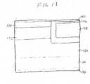
- FIG. 11is a schematic illustration of a UMOSFET/UMISFET device according to another preferred embodiment of the invention.
- FIG. 12is a schematic illustration of a DMOSFET/DMISFET device according to another preferred embodiment of the invention.
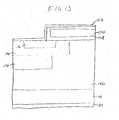
- FIG. 13is a schematic illustration of a power Insulated Gate Bipolar Transistor (power IGBT) device according to another preferred embodiment of the invention.
- FIG. 14is a schematic illustration of a power vertical JFET device according to another preferred embodiment of the invention.
- FIG. 15schematically illustrates a possible way of implementing a cascode configuration according to another preferred embodiment of the invention.
- FIG. 16is a schematic illustration of an integrated approach to a cascode configuration where a low voltage GaN normally-off FET is integrated on the same substrate as a vertical JFET according to another preferred embodiment of the invention.
- FIG. 17is a schematic illustrating an examples of a HEMT array according to another preferred embodiment of the invention.
- a homoepitaxial GaN based electronic device structureis formed by epitaxial growth of a number of GaN based semiconductor layers on a single crystal GaN substrate.
- a homoepitaxial GaN based electronic deviceis an electronic device with a GaN substrate and at least one GaN based semiconductor layer formed on the substrate.
- the at least one GaN based semiconductor layercomprises Al x In y Ga 1-x-y N, where 0 ⁇ x ⁇ 1, 0 ⁇ y ⁇ 1, and 0 ⁇ x+y ⁇ 1.
- the homoepitaxial GaN based electronic devicemay have other epitaxial layers which are not GaN based, such as an AlN layer or an Al x In 1-x N layer, where 0 ⁇ x ⁇ 1.
- Gallium nitride-based electronic devicessuch as a transistor, rectifier, or thyristor, are grown homoepitaxially directly on a high-quality single crystal gallium nitride substrate, where the substrate has a low dislocation density and a low concentration of unintentional impurities.
- the GaN substrate for the device fabricationmay consist of, for example, a (0001)-oriented GaN wafer cut from a boule that was grown using a supercritical solvent at a temperature greater than about 550° C. and a pressure greater than about 5 kbar.
- one suitable process for forming the GaN substratecomprises providing a source gallium nitride, solvent, and mineralizer.
- the source gallium nitridemay comprise at least one of poorly-crystallized gallium nitride, well-crystallized gallium nitride, amorphous gallium nitride, polycrystalline gallium nitride, and combinations thereof.
- the source gallium nitridemay be provided “as-is” in its raw form.
- the source gallium nitridecan be compacted into a “pill” and/or sintered into a polycrystalline compact.
- the source gallium nitridecan be formed in situ.
- Gallium metalmay be provided, which then reacts with the ammonia solvent after sealing of the capsule and treatment at high pressure and high temperature to form source gallium nitride.
- the source gallium nitridemay then be combined with at least one of the mineralizer and solvent to form a mixture.
- the gallium nitride, solvent, and mineralizermay optionally be provided individually to the capsule as separate and distinct un-combined materials.
- the mixturewhich can comprise gallium nitride and at least one of the solvent and mineralizer, can be optionally compacted into a pill. However the compacting of the mixture need not be conducted in the gallium nitride growth process.
- the source gallium nitride, solvent, and mineralizer, whether as a mixture that is compacted or not compacted,are then placed inside a capsule.
- additional mineralizercan also be added to the capsule.
- the capsulewhich will be described hereinafter, can then be filled with a nitrogen-containing solvent, for example at least one of ammonia or hydrazine, or an organic solvent, including but not limited to, methylamine, melamine, or ethylene diamine, and mixtures thereof.
- the capsuleis then sealed, disposed in a pressure cell, and subjected to high pressure and high temperature conditions in an appropriate high pressure high temperature (HPHT) system.
- HPHThigh pressure high temperature
- the HPHT conditionsare maintained for a length of time sufficient to dissolve the source gallium nitride and re-precipitate it onto at least one gallium nitride crystal, gallium nitride boule, or gallium nitride crystal seed.
- the resulting GaN crystalis a true single crystal, originating from a single seed rather than being formed by coalescence of multiple growth centers, and is free of grain boundaries, tilt boundaries, and the like.
- Maintaining HPHT conditionsyields large single gallium nitride crystals, for example single gallium nitride crystals having a diameter and thickness in a range from about 0.02 inch (about 0.05 cm) to about 12 inches (about 30 cm), for example a size in a range from about 2 inches to about 6 inches.
- the pressuremay be in a range from greater than about 5 kbar to about 80 kbar, and the temperature for the gallium nitride crystal growth process is in a range between about 550° C. and about 3000° C.
- the GaN single crystals thus formedare substantially transparent, with an optical absorption coefficient below 100 cm ⁇ 1 .
- the HPHT systemis then allowed to cool and the high pressure is relieved.
- the gallium nitride crystalsare removed from the HPHT system and pressure cell and washed in water and mineral acids.
- the mineral acids for washing the gallium nitride crystalsinclude, but are not limited to, hydrochloric acid (HCl) and nitric acid (HNO 3 ).
- the mineralizersmay comprise at least one of alkali and alkaline-earth nitrides, such as at least one of Li 3 N, Mg 3 N 2 , and Ca 3 Na 2 ; amides, such as LiNH 2 , NaNH 2 , and KNH 2 ; urea and related compounds, ammonium salts, such as NH 4 F and NH 4 Cl; halide, sulfide, and nitrate salts, such as NaCl, CeCl 3 , Li 2 S, and KNO 3 ; lithium salts, and combinations thereof.
- the mineralizersmay be provided as solids or as additives dissolved in fluids, such as solvents.
- alkaline-earth or rare-earth mineralizershave the additional advantage of acting as a getter for adventitious oxygen in the growth medium, allowing for the growth of undoped GaN crystals with low n-type carrier density.
- the mineralizercan be formed in situ. At least one of lithium, sodium, potassium, rubidium, cesium, magnesium, calcium, strontium, barium, or a rare-earth metal may be provided, which then react with the ammonia solvent to form the mineralizer.
- the capsuleis filled with a nitrogen-containing solvent, for example at least one of ammonia or hydrazine or an organic solvent, including, but not limited to methylamine, melamine, or ethylenediamine, without admitting air or water, which are undesirable in the gallium nitride formation process.
- a nitrogen-containing solventfor example at least one of ammonia or hydrazine or an organic solvent, including, but not limited to methylamine, melamine, or ethylenediamine
- a negative pressure sourcesuch as a vacuum manifold
- the capsuleis then chilled to a temperature below room temperature (preferably about ⁇ 72° C. or below) and vapor-phase solvent can be admitted to the manifold.
- the vapor-phase solventthen condenses in the capsule.
- the nitrogen-containing solventcomprises ammonia
- the condensationcan be performed at dry ice or liquid-nitrogen temperatures.
- the capsulecan then be isolated so as to seal the capsule by closing a valve to the negative pressure source.
- the capsulecan then be separated from at least one of the manifold or the valve by a pinching-off step using a cold welding apparatus, which is well known in the art.
- the pinching-off stepis particularly effective if the capsule is copper.
- the integrity of the sealmay be enhanced by optional arc-welding.
- the capsule and pressure cellcomprise any appropriate form that permit the gallium nitride growth process to withstand the high pressure and high temperature as embodied by the invention.
- the HPHT system that applies the high pressures and high temperaturescan comprise a press device, which may include at least one of a die and punch.
- the press devicemay comprise one of a piston-cylinder press; a belt press; a tetrahedral-, cubic-, or octahedral-anvil press; a recessed-anvil press; and a toroid-type press, each of which are known to those of skill in the art.
- Preferred capsules and pressure cellsare described in U.S. patent application Ser. Nos. 09/683,659 and 09/683,658, respectively, filed on Jan. 31, 2002, which are hereby incorporated by reference in their entirety.
- the GaN crystal formedis of high quality as determined by a measurement of dislocation density.
- the dislocation densitymay be determined by performing transmission electron microscopy (TEM) on a thin section, as is well known in the art.
- the GaN crystal formedcontains less than 10 5 threading dislocations per cm 2 , preferably less than 10 3 dislocations per cm 2 , and most preferably less than 10 2 dislocations per cm 2 .
- the GaN single crystalmay also be formed by other methods, such as the methods described in U.S. patent application entitled “IMPROVED GALLIUM NITRIDE CRYSTAL AND METHOD FOR MAKING”, Attorney Docket No. 040849-0216, filed concurrently with the present application.
- U.S. patent application entitled “IMPROVED GALLIUM NITRIDE CRYSTAL AND METHOD FOR MAKING”, Attorney Docket No. 040849-0216is hereby incorporated by reference in its entirety.
- the impurity levels in the raw materialssource gallium nitride, mineralizer, and solvent
- capsulesmust be limited to appropriately low levels.
- an oxygen concentration in the grown crystals below 3 ⁇ 10 18 cm ⁇ 3may be achieved by holding the total oxygen content in the raw materials and capsule below 15 parts per million, expressed with respect to the weight of the final crystal, and an impurity level below 3 ⁇ 10 17 cm ⁇ 3 may be achieved by holding the total oxygen content in the raw materials and capsule below 1.5 parts per million.
- the substrate or wafer for the device fabricationis cut from a boule.
- the wafermay comprise single crystal semi-insulating GaN, with an electrical resistivity greater than about 10 5 ⁇ -cm.
- the orientation used for growthis (0001) Ga in the preferred embodiment.
- the waferhas a dislocation density less than about 10 5 cm 2 , or more preferably below about 10 3 cm 2 .
- the substrates formedmay have carrier mobilities above about 100 cm 2 /V-s and strain, with respect to undoped GaN homoepitaxial layers, below about 0.005%.
- the substrateis polished to a mirror finish using mechanical-polishing techniques that are well known in the art.
- Subsurface damage on the wafer left over from the polishing processis removed by methods that are well known in the art, such as chemically-assisted ion beam etching or chemo-mechanical polishing. Residual damage may also be removed by heating the wafer to a temperature between about 900 and 1500° C. in an atmosphere containing ammonia at a partial pressure between 1 and 20,000 bar.
- the active device structuremay be fabricated by molecular beam epitaxy (MBE) or metalorganic vapor-phase epitaxy (MOVPE), also known as OMVPE or MOCVD. These deposition procedures are known in the art.
- MBEmolecular beam epitaxy
- MOVPEmetalorganic vapor-phase epitaxy
- the wafer or substrate 10is placed in a growth reactor (not shown), which is then evacuated. Residual surface defects are annealed, or adventitious contaminants removed, by heating the wafer to a temperature between about 900 and 1200° C. in an atmosphere containing ammonia at a partial pressure between 10 ⁇ 6 mbar and 1 bar.
- the device structureis formed by homoepitaxial deposition of a number of GaN based semiconductor layers.
- at least one GaN based semiconductor layeris formed on the substrate 10 .
- Each layer in the structureis formed by condensation of atomic species such as Ga, Al, In, and Si, or decomposition of organometallic precursors in a nitrogen-containing atmosphere on the substrate surface.
- the nitrogen-containing atmospherepreferentially includes nitrogen, ammonia or hydrazine and may be partially or completely decomposed before contact with the substrate surface.
- a carrier gassuch as H 2 or He may be used.
- Suitable organometallic precursors for MOVPEinclude, but are not limited to, trimethylgallium, Ga(CH 3 ) 3 , trimethylaluminum, Al(CH 3 ) 3 , and trimethylindum, In(CH 3 ) 3 .
- Suitable dopant precursorsinclude but are not limited to silane, SiH 4 , for n-type material, and bis-(cyclopentadienyl)magnesium (Mg(c-C 5 H 5 ) 2 ) or dimethyl zinc, Zn(CH 3 ) 2 , for p-type material.
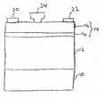
- FIGS. 1 - 3illustrate HEMT devices according to embodiments of the invention.
- FIG. 1illustrates a first embodiment of a HEMT.
- a buffer layer 12is formed on the substrate 10 .
- buffer layerhas a different meaning than the “buffer layer” often described in the GaN device art, which is a poorly-crystallized layer that acts as a transition layer between a non-GaN substrate such as sapphire or SiC and an epitaxial GaN layer.
- the buffer layer 12may be, for example, Al x In y Ga 1-x-y N, wherein 0 ⁇ x, y ⁇ 1, 0 ⁇ x+y ⁇ 1. Most preferably the buffer layer 12 comprises undoped GaN.
- the buffer layer 12may have a thickness between about 300 nm and 20 ⁇ m, or more preferably between 1 and 3 ⁇ m.
- the buffer layer 12will contain a two-dimensional electron gas (2DEG) and act as a channel layer.
- the carrier concentration in the buffer layer 12is preferably below 5 ⁇ 10 16 cm ⁇ 3 , and more preferably below 10 15 cm ⁇ 3 .
- the outermost portion of the substrate 10 itselfcan be utilized as the 2DEG region.
- a barrier layer 14is formed on the buffer layer 12 .
- the barrier layer 14has a wider bandgap than the buffer layer 12 .
- the barrier layer 14may comprise Al x In y Ga 1-x-y N, wherein 0 ⁇ x, y ⁇ 1, 0 ⁇ x+y ⁇ 1, and may comprise for example, Al x Ga 1-x N, where x ⁇ 0.2-0.3.
- the incorporation of In into the Al x In y Ga 1-x-y N barrier layer, with y ⁇ 0.22 xenables the barrier layer 14 to be approximately lattice matched to the GaN buffer layer 12 despite having a larger bandgap.
- the barrier layermay also comprise two sub barrier layers 14 a and 14 b .
- the sub barrier layer 14 bmay be formed on the buffer layer 12 and may be AlN and the sub barrier layer 14 a may be formed on the sub barrier layer 14 b and may be AlGaN.
- the sub barrier layer 14 bis a higher-bandgap layer than the sub barrier layer 14 a , and may have, for example, a thickness between about 0.6 and 1.5 nm.
- the barrier layer 14may have a thickness between 5 nm and 50 nm, or more preferably between 15 and 25 nm.
- a source contact 20 , drain contact 22 and gate contact 24are formed on the top surface of the device.
- the source contact 20 and the drain contact 22are deposited on either side of the device as ohmic contacts to form the source and the drain regions.
- Suitable compositions for the source and drain contacts 20 and 22include Ti/Al/Ti/Au, Ti/Al/Ni/Au, and Ti/Al/Pt/Au stacks, wherein each layer of the stack is between about 10 and about 500 nm thick.
- the first Ti layeris preferably between 10 and 30 nm thick, the Al layer between 50 and 300 nm thick, and the outermost layers between 30 and 70 nm thick. Deposition may be achieved, for example, by electron beam evaporation, thermal evaporation, or other techniques.
- the source and drain contacts 20 and 22may have, for example, a length between about 50 and 1000 ⁇ m.
- the width of the source and drain contacts 20 and 22may be between about 20 and 200 ⁇ m, or more preferably between about 40 and 100 ⁇ m.
- the separation between the source and drain contacts 20 and 22may be between about 0.2 ⁇ m and about 10 ⁇ m, or more preferably between 0.5 and 2 ⁇ m.
- the structureis annealed, at a temperature between about 500° C. and 950° C., or preferably between about 750 and 870° C., in order to achieve an ohmic contact.
- the gate contact 24is deposited between the source and the drain contacts on top of the barrier layer 14 as a Schottky gate.
- the length of the gate contact 24may be between about 20 and 1000 ⁇ m, or more preferably between about 50 and 500 ⁇ m, and the width may be between about 50 nm and 1 ⁇ m.
- Suitable compositions for the gate contact 24include Ni/Au and Pt/Au stacks, wherein the first layer of the stack is between about 20 and 200 nm and the Au layer is between about 100 and 1000 nm thick. Deposition may again be achieved by electron beam evaporation, thermal evaporation, or other techniques. The structure is not annealed, so as to retain Schottky rectification behavior.
- the HEMT of FIG. 2is similar to that of FIG. 1.
- the HEMT of FIG. 2includes a contact layer 18 formed between the source and drain contacts 20 and 22 and the barrier layer 14 , and a trench formed in the contact layer 18 to expose the barrier layer 14 , with the gate contact 24 formed on the barrier layer 14 .
- the contact layer 18may comprise n-doped Al x In y Ga 1-x-y N, wherein 0 ⁇ x, y ⁇ 1, 0 ⁇ x+y ⁇ 1, and may comprise for example n-type GaN with a carrier concentration greater than about 2 ⁇ 10 18 cm ⁇ 3 .
- the contact layer 18may have a thickness, for example, of between 10 and 200 nm.
- the contact layer 18is less oxidation prone than the barrier layer 14 , due to a reduced Al concentration, and also forms more reliable ohmic contacts.
- the HEMT of FIG. 3is similar to that of FIG. 1.
- the channel layer 28has a narrower bandgap than the buffer layer 12 and will contain the 2DEG.
- the channel layer 28may comprise Al x In y Ga 1-x-y N, wherein 0 ⁇ x, y ⁇ 1, 0 ⁇ x+y ⁇ 1, and may be In x Ga 1-x N, where x ⁇ 0.05-0.15.
- the channel layer 28may have a thickness between 3 nm and 20 nm, or more preferably between 5 and 10 nm.
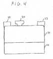
- FIG. 4illustrates an embodiment where the device is a MESFET.
- the MESFET deviceis essentially a simplified version of the HEMT, wherein GaN is used throughout the semiconductor structure and there is no barrier layer.
- a GaN channel layer 30is formed on the GaN substrate 10 .
- the source, drain and gate contacts 20 , 22 and 24may be formed in a similar fashion to that described with respect to FIG. 1.
- the ohmic contactsare improved by means of a contact layer (not shown) analogous to that shown in FIG. 2 or, more simply, by ion implantation of an n-type dopant such as Si into the region directly below the source and drain contacts 20 and 22 .
- the MESFETmay have somewhat inferior performance characteristics as compared to the HEMT but is simpler and cheaper to fabricate.
- the deviceis a MOSFET or MISFET.
- the MOSFET/MISFETis similar in structure to the MESFET of the embodiment of FIG. 4, except that the gate contact 24 is separated from the channel layer 30 by an insulating layer 32 , an oxide for a MOSFET or an insulating dielectric for a MISFET.
- the MOSFET/MISFETis particularly suitable for power electronic applications, as the presence of the oxide or insulator layer protects the GaN layer from oxidation during operation at high currents and/or elevated temperatures.
- Suitable compositions for the oxide of the insulating layer 32 for a MOSFETinclude at least one of SiO 2 , Sc 2 O 3 , MgO, Ga 2 O 3 , and R 2 O 3 , where R is a rare-earth element such as Gd.
- Suitable compositions for an insulating dielectric insulating layer 32 for the MISFETinclude AlN and Si 3 N 4 .
- An oxide or insulating layermay also be used to separate the gate from the barrier layer in the HEMT structure of FIG. 1.
- the deviceis an HBT.
- HBTsare particularly useful for the highest-frequency applications of GaN devices.
- the HBTcan be fabricated in either a npn configuration or a pnp configuration.
- fabrication of only the npn configurationwill be described in detail but fabrication of the pnp configuration is directly analogous with p-type layers of the npn substituted with n-type layers of the pnp configuration and vice versa.
- the substrate 10may be a bulk GaN substrate which is semi-insulating, and may have a resistivity greater than 10 5 ⁇ -cm.
- the substrate 10may also be n-type, preferably with a carrier concentration greater than about 2 ⁇ 10 18 cm ⁇ 3 .
- a collector layer 42is formed over the substrate 10 .
- the collector layer 42may be an n-type layer of Al x In y Ga 1-x-y N, wherein 0 ⁇ x, y ⁇ 1, 0 ⁇ x+y ⁇ 1, with a thickness between 200 nm and 5000 nm, or more preferably between 400 and 800 nm.
- the collector layer 42may comprise n-GaN or n-Al x Ga 1-x N, wherein 0 ⁇ x ⁇ 1 and is doped with a carrier concentration between about 1 ⁇ 10 16 and about 5 ⁇ 10 16 cm ⁇ 3 .
- a subcollector layer 40may be formed between the collector layer 42 and the substrate 10 , particularly when substrate 10 is semi-insulating.
- the subcollector layer 40may comprise, for example, n + doped GaN.
- the thickness of the subcollector layer 40may be between about 0.2 and 5 ⁇ m, or preferably between about 1 and 2 ⁇ m, and may have a carrier concentration greater than about 2 ⁇ 10 18 cm ⁇ 3 .
- Subcollector contacts 52which may be ohmic, are formed on the top surface of the subcollector layer 40 . The purpose of the subcollector layer 40 is to improve the performance of the ohmic subcollector contact 52 and, in the case of a semi-insulating substrate, to provide an ohmic contact to the collector layer.
- a base layer 44is formed on the collector layer 42 .
- the base layer 44may comprise p-type Al x In y Ga 1-x-y N, wherein 0 ⁇ x, y ⁇ 1, 0 ⁇ x+y ⁇ 1, with a thickness between 10 nm and 1000 nm, or more preferably between 50 and 200 nm.
- the base layer 44may comprise p + -GaN doped with a carrier concentration above about 2 ⁇ 10 18 cm ⁇ 3 .
- the base layer 44may also be graded from GaN, at the contact with the collector layer, to Al x Ga 1-x N with x ⁇ 0.05 near the top surface of the base layer 44 .
- a p-Al x Ga 1-x N/GaN superlatticemay be deposited on the top surface of the base layer 44 .
- the emitter layer 46is formed on the base layer 44 .
- the emitter layer 46may comprise n-type Al x In y Ga 1-x-y N, wherein 0 ⁇ x, y ⁇ 1, 0 ⁇ x+y ⁇ 1, with a thickness between 0.5 nm and 1000 nm, or more preferably between 50 and 300 nm.
- the emitter layer 46has as wider bandgap than the base layer 44 .
- the emitter layer 46comprises n-Al x Ga 1-x N, wherein 0.15 ⁇ x ⁇ 0.25 and may be doped with a carrier concentration >2 ⁇ 10 18 cm ⁇ 3 .
- the composition of the emitter layer 46is graded from n-Al x Ga 1-x N with x ⁇ 0.05, at the contact to the base layer 44 to n-GaN near the top surface of the emitter layer 46 .
- a cap layer 48is formed on the emitter layer 46 .
- the cap layer 48may comprise n + -GaN, with a thickness of about 100 nm and a carrier concentration greater than about 2 ⁇ 10 18 cm ⁇ 3 .
- the layersare etched to expose the base layer 44 and, if a top-facing collector contact is desired, a deeper via is etched to expose the subcollector layer 40 .
- Collector, base, and emitter contacts 52 , 54 and 56are formed.
- the contactsare preferably ohmic metallic contacts.
- the emitter contact 56is deposited on top of the cap layer 48
- the base contact 54is deposited on the base layer 44 after etching to expose the latter.
- a collector contact 52is deposited on the subcollector layer 40 , as described above.
- the bulk GaN substrateis n-type, with a carrier concentration greater than about 2 ⁇ 10 18 cm ⁇ 3 , and a collector contact 50 is deposited on the back surface of the substrate 10 , opposite the device structure.
- Suitable compositions for the n-type collector and emitter contactsinclude Ti/Al/Ti/Au, Ti/Al/Ni/Au, and Ti/Al/Pt/Au stacks, wherein each layer of the stack is between about 10 and about 500 nm thick, and deposition is achieved by electron beam evaporation, thermal evaporation, or other techniques.
- the first Ti layeris preferably between 10 and 30 nm thick, the Al layer between 50 and 300 nm thick, and the outermost layers between 30 and 70 nm thick.
- Suitable compositions for the p-type contactsinclude Ni/Au and Pt/Au stacks, wherein the first layer is between about 20 and 200 nm and the Au layer is between about 100 and 1000 nm thick. Following the depositions the structure is annealed, at a temperature between about 500° C. and 950° C., or preferably between about 750 and 870° C., in order to achieve an ohmic contact.
- a pnp HBTmay be formed by substituting the p-type layers of the pnp HBT with the n-type layers of the npn HBT and vice versa.
- FIG. 7illustrates another embodiment, where the device is a BJT.
- the BJT device of FIG. 7is similar to the HBT of FIG. 6.
- the BJT structureis a simplified version of the HBT, in which unalloyed GaN comprises all the semiconductor layers.
- the BJT device of FIG. 7is the same as the device of FIG. 6, except that unalloyed GaN is substituted for alloyed GaN layers.
- FIG. 8illustrates another embodiment, where the device is a Schottky rectifier.
- the Schottky rectifierincludes a GaN substrate 10 .
- the GaN substrate 10may be n-type, preferably with a carrier level greater than about 2 ⁇ 10 18 cm ⁇ 3 .
- a voltage blocking layer 70is formed on the substrate 10 .
- the voltage blocking layer 70may comprise undoped Al x In y Ga 1-x-y N, wherein 0 ⁇ x, y ⁇ 1, 0 ⁇ x+y ⁇ 1, with a thickness between 1 and 500 ⁇ m, or more preferably between 50 and 200 ⁇ m.
- the voltage blocking layer 70has greater thickness for higher blocking voltage requirements.
- the carrier concentration in the voltage blocking layer 70is preferably low, for example below 5 ⁇ 10 16 cm ⁇ 3 and more preferably below 10 15 cm ⁇ 3 .
- the Schottky rectifieremploys a p-type GaN substrate and p-type epilayer.
- a series of guard rings 72 and junction barrier control rings 74are formed on the voltage blocking layer 70 .
- the purpose of the guard rings 72is to reduce electric field crowding at the boundary of the subsequently formed oxide and contact and to increase the blocking voltage.
- the guard rings 72 and junction barrier control rings 74may be formed on the voltage blocking layer 70 by ion implantation, for example.
- the ions for implantingmay be Mg or Zn, for example.
- the carrier level in the region of the ringsis preferably greater than about 2 ⁇ 10 17 cm ⁇ 3 .
- An insulator layer 76is formed on the voltage blocking layer 70 .
- the insulator layer 76may comprise, for example, at least one of SiO 2 , Sc 2 O 3 , MgO, Ga 2 O 3 , and R 2 O 3 , where R is a rare-earth element such as Gd.
- the insulator layer 76covers the guard rings 72 , but not the junction barrier control rings 74 .
- a voltage blocking layer contact 80 and substrate contact 60are formed respectively on the voltage blocking layer 70 and the substrate 10 .
- the substrate contact 60is preferably an n-type contact (contacting an n-type layer) and may comprise a sequence of layers such as a Ti/Al/Ti/Au, Ti/Al/Ni/Au, or Ti/Al/Pt/Au stack, wherein each layer is between about 10 and about 500 nm thick.
- the deposition of the substrate contact 60may be achieved, for example, by electron beam evaporation, thermal evaporation, or other techniques.
- the first Ti layeris preferably between 10 and 30 nm thick, the Al layer between 50 and 300 nm thick, and the outermost layers of the contact 60 between 30 and 70 nm thick.
- the structureis annealed, at a temperature between about 500° C. and 950° C., or preferably between about 750 and 870° C., in order to achieve an ohmic contact.
- Suitable compositions for the voltage blocking layer contact 80include Ti/Pt/Au, Ni/Au and Pt/Au stacks, wherein the first layer(s) is(are) between about 20 and 200 nm and the Au layer is between about 100 and 1000 nm thick. After the voltage blocking layer contact 80 is formed, the device structure is not annealed at high temperature, so as to retain Schottky contact characteristics.
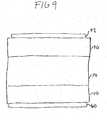
- FIG. 9illustrates another embodiment of the invention where the device is a p-i-n rectifier.
- the device structure of the p-i-n rectifier of FIG. 9is similar to that of the Schottky rectifier of FIG. 8 described above.
- the p-i-n rectifier of FIG. 9also includes guard rings on the voltage blocking layer 70 and an insulating layer analogous to those in FIG. 8.
- Contact layer 90is formed directly on the voltage blocking layer 70 .
- the contact layer 90may comprise, for example, p-GaN.
- the contact layer 90may have a thickness, for example, of between about 100 and 1000 nm, and more preferably between about 300 and about 700 nm.
- the contact layer 90may have a carrier concentration greater than about 2 ⁇ 10 18 cm ⁇ 3 .
- the p-i-n rectifier of FIG. 9also includes a substrate contact 60 in a similar fashion to the device of FIG. 8, which may be an n-type contact.
- the p-i-n rectifier of FIG. 9also includes an ohmic contact layer contact 92 .
- Suitable compositions for the contact layer contact 92include, for example, Ni/Au and Pt/Au stacks, wherein the first layer is between about 20 and 200 nm and the Au layer is between about 100 and 1000 nm thick. Following the depositions of the substrate contact 60 and the contact layer contact 92 , the structure is annealed at a temperature between about 500° C. and 950° C., or preferably between about 750 and 870° C., in order to achieve ohmic contacts.
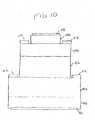
- FIG. 10illustrates another embodiment of the invention where the device is a thyristor.
- the thyristorcan be fabricated in either a npn(N)p configuration, or a pnp(P)n configuration.
- fabrication of only the npn(N)p configurationwill be described in detail but fabrication of the pnp(P)n configuration is directly analogous.
- the pnp(P)n configurationmay be formed by substituting the p-type layers with a corresponding n-type layer of the npn(N)p configuration and vice versa.
- the thyristor of FIG. 10includes a GaN substrate 10 .
- the GaN substrate 10may be semi-insulating, with a resistivity greater than 10 5 ⁇ -cm, or may be n-type, preferably with a carrier level greater than about 2 ⁇ 10 18 cm ⁇ 3 .
- a voltage blocking layer 102is formed over the substrate 10 .
- the voltage blocking layer 102may be an undoped layer of Al x In y Ga 1-x-y N, wherein 0 ⁇ x, y ⁇ 1, 0 ⁇ x+y ⁇ 1, with a thickness between 1 and 500 ⁇ m, or more preferably between 50 and 200 ⁇ m.
- the voltage blocking layer 102has greater thickness for higher blocking voltage requirements.
- the carrier concentration in the voltage blocking layer 102is preferably low, for example below 5 ⁇ 10 16 cm ⁇ 3 and more preferably below 10 15 cm ⁇ 3 .
- a first doped layer 100may be optionally formed between the substrate 10 and the voltage blocking layer 102 .
- the first doped layer 100may be a n + doped GaN layer deposited on the substrate 10 , with a thickness between about 0.2 and 5 ⁇ m or preferably between about 1 and 2 ⁇ m, and a carrier concentration greater than about 2 ⁇ 10 18 cm ⁇ 3 . If the bulk GaN substrate 10 is semi-insulating, doped layer contacts 112 are made on the top surface of the first doped layer 100 .
- the purpose of the first doped layer 100is to improve the performance of the ohmic contact of the contacts to the substrate 10 and, in the case of a semi-insulating substrate, to provide an electrical contact.
- a second doped layer 104is formed on the voltage blocking layer 102 .
- the second doped layer 104may comprise, for example, n-type Al x In y Ga 1-x-y N, wherein 0 ⁇ x, y ⁇ 1, 0 ⁇ x+y ⁇ 1, with a thickness between 100 nm and 3000 nm, or more preferably between 500 and 700 nm.
- the second doped layer 104may have a carrier concentration of about 2 ⁇ 10 17 cm ⁇ 3 .
- the second doped layer 104may comprise n-GaN.
- a n-A x Ga 1-x N/GaN superlatticemay be deposited on the top surface of the second doped layer 104 .
- a cap layer 106is formed on the second doped layer 104 .
- the cap layer 106may comprise p + -GaN, and may have a thickness of about 500 nm and a carrier concentration greater than about 2 ⁇ 10 18 cm ⁇ 3 .
- Doped layer contacts 112 , voltage blocking layer contacts 114 and cap layer contact 116are formed on respectively the first doped layer 100 , second doped layer 104 and cap layer 106 .
- the layersmay be etched as appropriate to expose the appropriate layers.
- a bottom contact 110may be deposited on the back surface of the substrate 10 , for example, if the bulk GaN substrate 10 is n + -type.
- Suitable compositions for the n-type contactsinclude Ti/Al/Ti/Au, Ti/Al/Ni/Au, and Ti/Al/Pt/Au stacks, wherein each stack layer is between about 10 and about 500 nm thick, and deposition is achieved by electron beam evaporation, thermal evaporation, or other techniques.
- the first Ti layeris preferably between 10 and 30 nm thick, the Al layer between 50 and 300 nm thick, and the outermost layers between 30 and 70 nm thick.
- Suitable compositions for the p-type contactsinclude Ni/Au and Pt/Au stacks, wherein the first layer of the stack is between about 20 and 200 nm and the Au layer is between about 100 and 1000 nm thick. Following the depositions the structure is annealed, at a temperature between about 500° C. and 950° C., or preferably between about 750 and 870° C., in order to achieve ohmic contacts for the contact layers.
- FIGS. 11 and 12illustrate two other embodiments of the invention where the devices are power vertical MOSFETs or MISFETs (MOSFET for devices with a gate oxide, and MISFET for devices with a gate insulating layer).
- FIG. 11illustrates a UMOSFET/UMISFET
- FIG. 12illustrates a DMOSFET/DMISFET.
- the “U” in UMOSFET or UMISFETrefers to the shape of the trench structure where the gate is located.
- the “D” in DMOSFET or DMISFETrefers to the diffusion or doubly-implanted layers in the structure.
- MOSFET/MISFET vertical structureis similar in operation to a lateral MOSFET/MISFET device, but the current flow is directed vertically through the substrate in the vertical structure.
- the descriptions of UMOSFETs and DMOSFETs belowinvolve npn-type structures, but analogous devices with pnp structures are also possible.
- the deviceincludes a GaN substrate 10 .
- the GaN substrate 10may be n-type, for example.
- a voltage blocking layer 120is formed over the substrate 10 and may be, for example, n-type with a carrier concentration of about 1 ⁇ 10 17 to 5 ⁇ 10 16 cm ⁇ 3 .
- the voltage blocking layer 120may be, for example, GaN, and may have a thickness, for example, of greater than about 400 nm.
- a p-type channel layer 122is formed over the voltage blocking layer 120 .
- the p-type channel layer 122may be, for example, p-doped to a carrier concentration of about 2 ⁇ 10 17 cm ⁇ 3 .
- the p-type channel layer 122may be, for example, GaN, and may have a thickness, for example, of between about 100 and 200 nm.
- a n-type source layer 124is formed over the p-type channel layer 122 .
- the n-type source layer 124may be, for example, GaN.
- a trenchmay be etched into voltage blocking layer 120 , p-type channel layer 122 and n-type source layer 124 to allow for formation of the gate insulator 126 and metal gate 128 .
- the trenchmay be formed by plasma etching, for example.
- the gate insulator 126 materialmay be, for example, an oxide such as at least one of SiO 2 , Sc 2 O 3 , MgO, Ga 2 O 3 , and R 2 O 3 , where R is a rare-earth element such as Gd.
- Suitable compositions for a non-oxide gate insulator 126include AlN and Si 3 N 4 .
- the metal gate 128is then deposited into the trench on the gate insulator 126 , then overcoated with oxide or non-oxide insulating material to form some of the gate insulator 126 over the metal gate 128 except above one or more points (not shown) where electrical contacts are made to the metal gate 128 .
- a source contact 130is then formed over the n-type source layer 124 , while a bottom contact 132 is formed on the back surface of the substrate 10 .
- Suitable compositions for contacts 130 and 132include Ti/Al/Ti/Au, Ti/Al/Ni/Au, and Ti/Al/Pt/Au stacks, wherein each stack layer is between about 10 and about 500 nm thick, and deposition is achieved by electron beam evaporation, thermal evaporation, or other techniques.
- the first Ti layeris preferably between 10 and 30 nm thick, the Al layer between 50 and 300 nm thick, and the outermost layers between 30 and 70 nm thick.
- the structureis annealed, at a temperature between about 500° C. and 950° C., or preferably between about 750 and 870° C., in order to achieve ohmic contacts for the contact layers.
- FIG. 12illustrates a DMOSFET device structure.
- the DMOSFETis similar to the UMOSFET, however, the gate insulator 126 and the metal gate 128 are not formed in a trench, but over the p-type layer 122 and n-type layer 124 .
- the p-type layer 122 and n-type layer 124may be formed in the voltage blocking layer 120 using selective area ion implantation, diffusion doping, or, alternatively, epitaxy followed by etching, additional epitaxy, and re-planarization.
- the gate insulator 126 and the metal gate 128act to modulate the portion of the channel layer 122 under the gate.
- Currentflows laterally from source 124 through channel 122 and then vertically through voltage blocking layer 120 to bottom contact 132 .
- the voltage blocking layersupports the blocking voltage under normally off conditions.
- This vertical device structuregreatly benefits from the absence of a band offset and voltage drop at the epi/substrate interface of the homoepitaxial device structure compared to a heteroepitaxial structure.
- the reduced dislocation density in the homoepitaxially grown voltage blocking layer 120and resulting longer carrier lifetime gives rise to a conductivity modulation of the voltage blocking layer which will lower the overall power loss of the device.
- FIG. 13illustrates another embodiment of the invention where the device is a power Insulated Gate Bipolar Transistor (power IGBT).
- the power IGBTcan be fabricated in either n + -p-n-p + or p + -n-p-n + configuration, but for simplicity will only be described in detail as n + -p-n-p + .
- Fabrication of the p + -n-p-n +is directly analogous, with the p-doped layers being substituted for n-doped layers and vice versa.
- the operation and fabrication of the power IGBTis similar to that of the power lateral DMOSFET of the embodiment of FIG. 12.
- the substrateis of the opposite polarity to the blocking layer, effectively making a DMOSFET in series with a p-i-n junction diode such that the device will only conduct current in one direction.
- the power IGBTincludes a p-type substrate 10 , an n-type voltage blocking layer 140 formed on the p-type substrate 10 , a heavily doped p-type base layer 142 formed in and over the blocking layer 140 , a lightly doped p-type base layer 144 formed in and over the blocking layer 140 , and over the heavily doped p-type base layer 142 , and an n-type emitter 146 formed in the lightly doped p-type base layer 144 .
- a gate insulating layer 148is formed over the doped layer and partially surrounds a metal gate 150 .
- an emitter contact 152is formed over and contacting the emitter 146 , and a bottom contact 154 is formed on the reverse side of the substrate 10 .
- the substratemay be p-doped GaN.
- the voltage blocking layer 140may be n-doped GaN, for example, with a doping concentration of about 1 ⁇ 10 16 to 5 ⁇ 10 16 cm ⁇ 3 , and with a thickness of greater than about 400 nm.
- the heavily doped p-type base layer 142may be, for example, GaN with a doping concentration of about 2 ⁇ 10 18 cm ⁇ 3 , and with a thickness of between about 100 and 200 nm.
- the lightly doped p-type base layer 144may be, for example, GaN with a doping concentration of about 2 ⁇ 10 17 cm ⁇ 3 , and with a thickness of between about 100 and 200 nm.
- the n-type emitter 146may be, for example, GaN with a doping concentration of about 1 ⁇ 10 18 cm ⁇ 3 , and with a thickness of between about 50 and 100 nm.
- the gate insulator 148 materialmay be, for example, an oxide such as at least one of SiO 2 , Sc 2 O 3 , MgO, Ga 2 O 3 , and R 2 O 3 , where R is a rare-earth element such as Gd.
- Suitable compositions for a non-oxide gate insulator 148include AlN and Si 3 N 4 .
- the metal gate 150may be, for example, Mo.
- Suitable compositions for the emitter contact 152include Ti/Al/Ti/Au, Ti/Al/Ni/Au, and Ti/Al/Pt/Au stacks, wherein each layer of the stack is between about 10 and about 500 nm thick, and deposition is achieved by electron beam evaporation, thermal evaporation, or other techniques.
- the first Ti layeris preferably between 10 and 30 nm thick, the Al layer between 50 and 300 nm thick, and the outermost layers between 30 and 70 nm thick.
- Suitable compositions for the bottom contact 154include Ni/Au and Pt/Au stacks, wherein the first layer is between about 20 and 200 nm and the Au layer is between about 100 and 1000 nm thick. Following the depositions the structure is annealed, at a temperature between about 500° C. and 950° C., or preferably between about 750 and 870° C., in order to achieve an ohmic contact.
- the n-type emitter layer 146 , the lightly doped p-type base layer 144 and the heavily doped p-type base layer 142may be created using selective area ion implantation, diffusion doping, or, alternatively, epitaxy followed by etching a trench, epitaxial filling of the trench, and re-planarization, for example.
- the purpose of the heavily doped p-type base layer 142is to suppress latch-up of the parasitic thyristor inherent to the device structure.
- the n-type voltage blocking layer 140will have a thickness and doping concentration that varies according to the blocking voltage desired. Like the DMOSFET and UMOSFET described above, this vertical device structure greatly benefits from the higher conductivity of the bulk GaN substrate. In addition, the reduced dislocation density in the homoepitaxially grown blocking layer, and resulting longer carrier lifetime gives rise to a conductivity modulation of the drift region which will lower the overall power loss of the device.
- FIG. 14illustrates another embodiment of the invention where the device is a power vertical JFET.
- the power vertical JFETincludes a n-type substrate 10 , an lightly doped n-type voltage blocking layer 160 formed on the n-type substrate 10 , a heavily doped n-type source layer 164 formed over the blocking layer 160 , a p-type gate layer 162 formed in and over the blocking layer 160 .
- a source contact layer 166is formed on the source layer 164 .
- a gate contact layer 168is formed on the gate layer 162 .
- a drain contact 170is formed on the reverse side of the substrate 10 .
- the current flowis directed vertically from the source layer 164 through the blocking layer 160 through substrate 10 .
- This deviceis a normally-on device. It is turned off by applying a negative bias to the pn junction between the source and gate layers 164 and 162 . With sufficient reverse bias on the pn junction, the depletion layer expands below the source layer 164 and pinches off the channel, preventing vertical current flow.
- This structureconsists of a buried channel where issues of surface traps and insulating layers are minimized. The large critical field of GaN allows this structure to have a high blocking voltage with low on-state resistance. Also, this device is a unipolar majority carrier device and is capable of high switching speed due to the absence of stored minority charge. This device can be designed to be normally off by reducing the width of source layer 164 to below approximately 1 micron such that the built-in depletion region extending from gate layer 162 pinches off the channel under source layer 164 .
- the substratemay be n-type GaN.
- the voltage blocking layer 160may be n-type GaN, for example, with a doping concentration of about 1 ⁇ 10 16 to 5 ⁇ 10 16 cm ⁇ 3 , and with a thickness of greater than about 5000 nm.
- the source layer 164may be, for example, n-type GaN with a doping concentration of about 1 ⁇ 10 18 cm ⁇ 3 , and with a thickness of between about 100 and 500 nm.
- the gate layer 162may be, for example, p-type GaN with a doping concentration of greater than about 5 ⁇ 10 17 cm ⁇ 3 , and with a thickness of between about 750 and 2000 nm.
- the source contact 166may be, for example, Ti/Al/Ti/Au.
- the gate contact 168may be, for example, Ni/Au.
- the drain contact 170may be, for example, Ti/Al/Ti/Au.
- the thickness and doping valuesare for a blocking voltage on the order of 1000V. In general, the doping and thickness values would depend on the desired blocking voltage characteristic.
- the blocking layer 160 and source layer 164may be grown epitaxially in a preferred embodiment, while the gate layer 162 may be formed by implanting with a p-type implant species (such as Mg) into the blocking layer 160 and source layer 164 .
- the gate layer 162may be formed by epitaxially re-growth after trench etching of the region where the gate layer 162 is to be grown and then planarized to smooth the top surface.
- FIG. 15illustrates a GaN vertical JFET 180 in cascode with a low-voltage discrete silicon MOSFET 182 .
- 182may instead constitute a discrete SiC or a GaN based low-voltage normally-off FET.
- FIG. 16illustrates another embodiment of the invention demonstrating an integrated approach to the cascode configuration where a low voltage GaN normally-off FET is integrated as a part of the structure on the same substrate with a vertical JFET.
- the integrated structureincludes a substrate 10 , a n-type blocking layer 192 formed over the substrate 10 , a buried p-type gate layer 194 formed in the blocking layer 192 , a p-type well layer 196 formed on the buried gate layer 194 , n-type source 198 and n-type drain 200 formed in the well layer 196 , and a p-type field stop 202 formed in the blocking 192 and lateral to the n-type source 198 and n-type drain 200 .
- the devicealso includes a source contact 206 on the source 198 , a gate contact 208 on an insulating layer 204 which is on the channel region in well layer 196 between the source 198 and drain 200 , a field stop contact 210 on the field stop 202 and a drain contact 212 on the reverse side of the substrate 10 .
- the substratemay be n-type GaN.
- the blocking layer 192may be n-type GaN, for example, with a doping concentration of about 1 ⁇ 10 16 to 5 ⁇ 10 16 cm ⁇ 3 , and with a thickness of greater than about 5000 nm.
- the buried gate layer 194may be p-type GaN, for example, with a doping concentration of about 1 ⁇ 10 19 , and with a thickness of between about 100 and 500 nm.
- the well layer 196may be p-type GaN, for example, with a doping concentration of about 1 ⁇ 10 17 , and with a thickness of between about 500 and 2000 nm.
- the field stop layer 202may be p-type GaN, for example, with a doping concentration of about 1 ⁇ 10 19 , and with a thickness of between about 100 and 500 nm.
- the source and drain 198 and 200may be n-type GaN, for example, with a doping concentration of about 1 ⁇ 10 19 , and with a thickness of between about 100 and 500 nm.
- the insulating layer 204may be an oxide, or other insulating layer, for example, Suitable compositions for the source contact 206 and drain contact 212 include Ti/Al/Ti/Au. Suitable compositions for gate contact 208 and field stop contact 210 include Ni/Au.
- the devices described in the above embodimentsmay be discrete, for example for HBT, Schottky rectifier, p-i-n rectifier, thyristor, or vertical MOSFET or JFET devices, or they may consist of arrays, for example for the HEMT, MESFET, and MOSFET/MISFET devices.
- FIG. 17An example of a HEMT array is shown in FIG. 17.
- the array deviceincludes gate contacts 224 , drain contacts 222 , and source contacts 220 . External electrical connection to the array of source contacts is made by means of air bridges 230 , which are bonded to source contacts 220 , but pass over drain contacts 222 and gate contacts 224 without making any electrical contact.
- the array deviceincludes an active region (not shown) below the contacts, where the array device includes a number of HEMT components in an array.
Landscapes
- Engineering & Computer Science (AREA)
- Chemical & Material Sciences (AREA)
- Microelectronics & Electronic Packaging (AREA)
- Power Engineering (AREA)
- Condensed Matter Physics & Semiconductors (AREA)
- General Physics & Mathematics (AREA)
- Manufacturing & Machinery (AREA)
- Computer Hardware Design (AREA)
- Physics & Mathematics (AREA)
- Materials Engineering (AREA)
- Crystallography & Structural Chemistry (AREA)
- Metallurgy (AREA)
- Organic Chemistry (AREA)
- Inorganic Chemistry (AREA)
- Chemical Kinetics & Catalysis (AREA)
- General Chemical & Material Sciences (AREA)
- Junction Field-Effect Transistors (AREA)
- Electrodes Of Semiconductors (AREA)
Abstract
Description
- This application is related to U.S. patent application entitled “IMPROVED GALLIUM NITRIDE CRYSTAL AND METHOD FOR MAKING”, Attorney Docket No. 040849-0216, filed concurrently herewith.[0001]
- This invention is related generally to homoepitaxial gallium nitride (GaN) based electronic devices and specifically to homoepitaxial GaN based transistors, rectifiers, thyristors, and cascode switches.[0002]
- Gallium nitride (GaN) based electronic devices offer superior high voltage, high power, high temperature, and high frequency operation, as compared to analogous devices fabricated on silicon, gallium arsenide (GaAs) or indium phosphide (InP) substrates due to GaN's wide bandgap, high breakdown field, and high saturation velocity. A variety of types of GaN-based devices are of interest for microwave power amplifier and low-noise amplifier applications, including metal semiconductor field effect transistors (MESFETs), metal oxide field effect transistors (MOSFETs), metal insulator field effect transistors (MISFETs), bipolar junction transistors (BJTs). Heterojunction bipolar transistors (HBTs) and high electron mobility transistors (HEMTs), also known as heterojunction field-effect transistors (HFETs), modulation-doped field effect transistors (MODFETs), two-dimensional electron gas field effect transistors (TEGFETs), or selectively-doped heterostructure transistors (SDHTs), which take advantage of the bandgap engineering possible with III-V heterojunctions to provide considerably higher electron mobilities than analogous MESFETs. Additional GaN-based devices are of interest for power electronic applications, including thyristors, Schottky rectifiers, p-i-n diodes, power vertical MOSFETs, power vertical junction field effect transistors (JFETs), and cascode switches, which take advantage of GaN's wide bandgap, high breakdown field, high thermal conductivity, and high electron mobility.[0003]
- Typically, GaN-based electronic devices have employed heteroepitaxial growth of GaN and AlGaN on sapphire or SiC substrates. A thin low-temperature nucleation layer, AlN or GaN, also referred to as a buffer layer, is typically used in order to accommodate the lattice mismatch between GaN and the substrate and maintain an epitaxial relationship to the substrate. This approach suffers from a number of drawbacks, including: (i) generation of about 10[0004]10threading dislocations per cm2due to lattice mismatch, degrading device performance; (ii) excess strain in the device structure, due to thermal expansion mismatch, resulting in degraded performance, device yield, and reliability; and (iii) in the case of sapphire substrates, poor heat dissipation. Heteroepitaxial GaN-based electronic devices have been able to demonstrate performance levels that are satisfactory for some applications, but do not have the requisite level of reliability.
- At least one homoepitaxial GaN-based electronic device design, a HEMT, has been reported to date. Khan et al. [Appl. Phys. Lett. 76, 3807 (2000)] disclose the fabrication of an AlGaN/GaN HEMT on a bulk GaN substrate that was grown in a liquid Mg/Ga alloy at temperatures of 1300-1500° C. and N[0005]2pressures of 15-20 kbar. These substrates, however, have several disadvantages including: (i) a high concentration of Mg and O atoms, approximately 1019cm−3each [J. I. Pankove et al., Appl. Phys. Lett. 74, 416 (1999)], which could potentially diffuse into device structures during high temperature processing; and (ii) relatively poor thermal conductivity. Dopants may diffuse into the undoped GaN buffer layer, in which transport by the two-dimensional electron gas is designed to occur, degrading carrier mobility. In addition, the presence of the point defects scatters phonons in the bulk GaN substrate and degrades thermal conductivity, which is detrimental to achieving theoretical performance levels in GaN-based HEMTs. In fact, the homoepitaxial HEMT reported by Khan et al. actually had a slightly inferior performance to a similar device fabricated on a SiC substrate.
- In accordance with one aspect of the present invention, there is provided a homoepitaxial gallium nitride based electronic device. The device comprises at least one epitaxial semiconductor layer disposed on a single crystal substrate comprised of gallium nitride, the substrate having a dislocation density less than about 10[0006]5per cm2, wherein the at least one epitaxial semiconductor layer is included in the electronic device which comprises one of a transistor, rectifier, thyristor, and cascode switch.
- In accordance with another aspect of the present invention, there is provided a method of forming an electronic device comprising: providing a single crystal substrate comprised of gallium nitride having a dislocation density less than about 10[0007]5per cm2; homoepitaxially forming at least one semiconductor layer on the substrate, wherein the electronic device is one of a transistor, rectifier, thyristor, and cascode switch.
- FIG. 1 is a schematic illustration of a HEMT device according to a preferred embodiment of the invention.[0008]
- FIG. 2 is a schematic illustration of a HEMT device according to another preferred embodiment of the invention.[0009]
- FIG. 3 is a schematic illustration of a HEMT device according to another preferred embodiment of the invention.[0010]
- FIG. 4 is a schematic illustration of a MESFET device according to another preferred embodiment of the invention.[0011]
- FIG. 5 is a schematic illustration of a MOSFET or MISFET device according to another preferred embodiment of the invention.[0012]
- FIG. 6 is a schematic illustration of a HBT device according to another preferred embodiment of the invention.[0013]
- FIG. 7 is a schematic illustration of a BJT device according to another preferred embodiment of the invention.[0014]
- FIG. 8 is a schematic illustration of a Schottky rectifier device according to another preferred embodiment of the invention.[0015]
- FIG. 9 is a schematic illustration of a p-i-n rectifier device according to another preferred embodiment of the invention.[0016]
- FIG. 10 is a schematic illustration of a thyristor device according to another preferred embodiment of the invention.[0017]
- FIG. 11 is a schematic illustration of a UMOSFET/UMISFET device according to another preferred embodiment of the invention.[0018]
- FIG. 12 is a schematic illustration of a DMOSFET/DMISFET device according to another preferred embodiment of the invention.[0019]
- FIG. 13 is a schematic illustration of a power Insulated Gate Bipolar Transistor (power IGBT) device according to another preferred embodiment of the invention.[0020]
- FIG. 14 is a schematic illustration of a power vertical JFET device according to another preferred embodiment of the invention.[0021]
- FIG. 15 schematically illustrates a possible way of implementing a cascode configuration according to another preferred embodiment of the invention.[0022]
- FIG. 16 is a schematic illustration of an integrated approach to a cascode configuration where a low voltage GaN normally-off FET is integrated on the same substrate as a vertical JFET according to another preferred embodiment of the invention.[0023]
- FIG. 17 is a schematic illustrating an examples of a HEMT array according to another preferred embodiment of the invention.[0024]
- Substrate Preparation.[0025]
- A homoepitaxial GaN based electronic device structure is formed by epitaxial growth of a number of GaN based semiconductor layers on a single crystal GaN substrate. Thus, in this application a homoepitaxial GaN based electronic device is an electronic device with a GaN substrate and at least one GaN based semiconductor layer formed on the substrate. The at least one GaN based semiconductor layer comprises Al[0026]xInyGa1-x-yN, where 0≦x≦1, 0≦y≦1, and 0≦x+y≦1. In addition to the GaN based semiconductors, the homoepitaxial GaN based electronic device may have other epitaxial layers which are not GaN based, such as an AlN layer or an AlxIn1-xN layer, where 0≦x≦1. Gallium nitride-based electronic devices, such as a transistor, rectifier, or thyristor, are grown homoepitaxially directly on a high-quality single crystal gallium nitride substrate, where the substrate has a low dislocation density and a low concentration of unintentional impurities.
- The GaN substrate for the device fabrication may consist of, for example, a (0001)-oriented GaN wafer cut from a boule that was grown using a supercritical solvent at a temperature greater than about 550° C. and a pressure greater than about 5 kbar.[0027]
- More specifically, one suitable process for forming the GaN substrate comprises providing a source gallium nitride, solvent, and mineralizer. The source gallium nitride may comprise at least one of poorly-crystallized gallium nitride, well-crystallized gallium nitride, amorphous gallium nitride, polycrystalline gallium nitride, and combinations thereof. The source gallium nitride may be provided “as-is” in its raw form. Alternatively, the source gallium nitride can be compacted into a “pill” and/or sintered into a polycrystalline compact. Alternatively, the source gallium nitride can be formed in situ. Gallium metal may be provided, which then reacts with the ammonia solvent after sealing of the capsule and treatment at high pressure and high temperature to form source gallium nitride.[0028]
- The source gallium nitride may then be combined with at least one of the mineralizer and solvent to form a mixture. The gallium nitride, solvent, and mineralizer may optionally be provided individually to the capsule as separate and distinct un-combined materials. The mixture, which can comprise gallium nitride and at least one of the solvent and mineralizer, can be optionally compacted into a pill. However the compacting of the mixture need not be conducted in the gallium nitride growth process.[0029]
- The source gallium nitride, solvent, and mineralizer, whether as a mixture that is compacted or not compacted, are then placed inside a capsule. Optionally, additional mineralizer can also be added to the capsule. The capsule, which will be described hereinafter, can then be filled with a nitrogen-containing solvent, for example at least one of ammonia or hydrazine, or an organic solvent, including but not limited to, methylamine, melamine, or ethylene diamine, and mixtures thereof. The capsule is then sealed, disposed in a pressure cell, and subjected to high pressure and high temperature conditions in an appropriate high pressure high temperature (HPHT) system. The HPHT conditions are maintained for a length of time sufficient to dissolve the source gallium nitride and re-precipitate it onto at least one gallium nitride crystal, gallium nitride boule, or gallium nitride crystal seed. The resulting GaN crystal is a true single crystal, originating from a single seed rather than being formed by coalescence of multiple growth centers, and is free of grain boundaries, tilt boundaries, and the like.[0030]
- Maintaining HPHT conditions yields large single gallium nitride crystals, for example single gallium nitride crystals having a diameter and thickness in a range from about 0.02 inch (about 0.05 cm) to about 12 inches (about 30 cm), for example a size in a range from about 2 inches to about 6 inches. The pressure may be in a range from greater than about 5 kbar to about 80 kbar, and the temperature for the gallium nitride crystal growth process is in a range between about 550° C. and about 3000° C. The GaN single crystals thus formed are substantially transparent, with an optical absorption coefficient below 100 cm[0031]−1.
- The HPHT system is then allowed to cool and the high pressure is relieved. The gallium nitride crystals are removed from the HPHT system and pressure cell and washed in water and mineral acids. The mineral acids for washing the gallium nitride crystals include, but are not limited to, hydrochloric acid (HCl) and nitric acid (HNO[0032]3).
- The mineralizers may comprise at least one of alkali and alkaline-earth nitrides, such as at least one of Li[0033]3N, Mg3N2, and Ca3Na2; amides, such as LiNH2, NaNH2, and KNH2; urea and related compounds, ammonium salts, such as NH4F and NH4Cl; halide, sulfide, and nitrate salts, such as NaCl, CeCl3, Li2S, and KNO3; lithium salts, and combinations thereof. The mineralizers may be provided as solids or as additives dissolved in fluids, such as solvents. The use of alkaline-earth or rare-earth mineralizers have the additional advantage of acting as a getter for adventitious oxygen in the growth medium, allowing for the growth of undoped GaN crystals with low n-type carrier density. Alternatively, the mineralizer can be formed in situ. At least one of lithium, sodium, potassium, rubidium, cesium, magnesium, calcium, strontium, barium, or a rare-earth metal may be provided, which then react with the ammonia solvent to form the mineralizer.
- The filling and sealing steps will now be described. The capsule is filled with a nitrogen-containing solvent, for example at least one of ammonia or hydrazine or an organic solvent, including, but not limited to methylamine, melamine, or ethylenediamine, without admitting air or water, which are undesirable in the gallium nitride formation process. To fill the capsule without admitting air or water, the capsule is filled and connected to a negative pressure source, such as a vacuum manifold, and evacuated. The capsule is then chilled to a temperature below room temperature (preferably about −72° C. or below) and vapor-phase solvent can be admitted to the manifold. The vapor-phase solvent then condenses in the capsule. For example, if the nitrogen-containing solvent comprises ammonia, the condensation can be performed at dry ice or liquid-nitrogen temperatures.[0034]
- The capsule can then be isolated so as to seal the capsule by closing a valve to the negative pressure source. The capsule can then be separated from at least one of the manifold or the valve by a pinching-off step using a cold welding apparatus, which is well known in the art. The pinching-off step is particularly effective if the capsule is copper. The integrity of the seal may be enhanced by optional arc-welding.[0035]
- The capsule and pressure cell comprise any appropriate form that permit the gallium nitride growth process to withstand the high pressure and high temperature as embodied by the invention. The HPHT system that applies the high pressures and high temperatures can comprise a press device, which may include at least one of a die and punch. For example, the press device may comprise one of a piston-cylinder press; a belt press; a tetrahedral-, cubic-, or octahedral-anvil press; a recessed-anvil press; and a toroid-type press, each of which are known to those of skill in the art. Preferred capsules and pressure cells are described in U.S. patent application Ser. Nos. 09/683,659 and 09/683,658, respectively, filed on Jan. 31, 2002, which are hereby incorporated by reference in their entirety.[0036]
- The foregoing description of the process for forming the GaN single crystal substrate is intended to be illustrative only, and should not be construed in any limiting sense. Other methods for forming the single crystal will be obvious to those skilled in the art, but are intended to fall within the scope of the present disclosure.[0037]
- The GaN crystal formed is of high quality as determined by a measurement of dislocation density. The dislocation density may be determined by performing transmission electron microscopy (TEM) on a thin section, as is well known in the art. The GaN crystal formed contains less than 10[0038]5threading dislocations per cm2, preferably less than 103dislocations per cm2, and most preferably less than 102dislocations per cm2.
- The GaN single crystal may also be formed by other methods, such as the methods described in U.S. patent application entitled “IMPROVED GALLIUM NITRIDE CRYSTAL AND METHOD FOR MAKING”, Attorney Docket No. 040849-0216, filed concurrently with the present application. U.S. patent application entitled “IMPROVED GALLIUM NITRIDE CRYSTAL AND METHOD FOR MAKING”, Attorney Docket No. 040849-0216, is hereby incorporated by reference in its entirety. In order to keep the concentration of undesired dopants, such as oxygen, to an acceptable level, the impurity levels in the raw materials (source gallium nitride, mineralizer, and solvent) and capsules must be limited to appropriately low levels. For example, an oxygen concentration in the grown crystals below 3×10[0039]18cm−3may be achieved by holding the total oxygen content in the raw materials and capsule below 15 parts per million, expressed with respect to the weight of the final crystal, and an impurity level below 3×1017cm−3may be achieved by holding the total oxygen content in the raw materials and capsule below 1.5 parts per million.
- After the crystal has been formed, the substrate or wafer for the device fabrication is cut from a boule. The wafer may comprise single crystal semi-insulating GaN, with an electrical resistivity greater than about 10[0040]5Ω-cm. The orientation used for growth is (0001) Ga in the preferred embodiment. The wafer has a dislocation density less than about 105cm2, or more preferably below about 103cm2. Furthermore, the substrates formed may have carrier mobilities above about 100 cm2/V-s and strain, with respect to undoped GaN homoepitaxial layers, below about 0.005%. The substrate is polished to a mirror finish using mechanical-polishing techniques that are well known in the art.
- Subsurface damage on the wafer left over from the polishing process is removed by methods that are well known in the art, such as chemically-assisted ion beam etching or chemo-mechanical polishing. Residual damage may also be removed by heating the wafer to a temperature between about 900 and 1500° C. in an atmosphere containing ammonia at a partial pressure between 1 and 20,000 bar.[0041]
- Device fabrication.[0042]
- Embodiments of the present invention are described below in detail with reference to the accompanying drawings. The same reference numerals denote the same parts throughout the drawings.[0043]
- The active device structure may be fabricated by molecular beam epitaxy (MBE) or metalorganic vapor-phase epitaxy (MOVPE), also known as OMVPE or MOCVD. These deposition procedures are known in the art.[0044]
- The wafer or[0045]
substrate 10 is placed in a growth reactor (not shown), which is then evacuated. Residual surface defects are annealed, or adventitious contaminants removed, by heating the wafer to a temperature between about 900 and 1200° C. in an atmosphere containing ammonia at a partial pressure between 10−6mbar and 1 bar. - The device structure is formed by homoepitaxial deposition of a number of GaN based semiconductor layers. Thus, at least one GaN based semiconductor layer is formed on the[0046]
substrate 10. Each layer in the structure is formed by condensation of atomic species such as Ga, Al, In, and Si, or decomposition of organometallic precursors in a nitrogen-containing atmosphere on the substrate surface. The nitrogen-containing atmosphere preferentially includes nitrogen, ammonia or hydrazine and may be partially or completely decomposed before contact with the substrate surface. A carrier gas such as H2or He may be used. - Suitable organometallic precursors for MOVPE include, but are not limited to, trimethylgallium, Ga(CH[0047]3)3, trimethylaluminum, Al(CH3)3, and trimethylindum, In(CH3)3. Suitable dopant precursors (if the layer is to be doped) include but are not limited to silane, SiH4, for n-type material, and bis-(cyclopentadienyl)magnesium (Mg(c-C5H5)2) or dimethyl zinc, Zn(CH3)2, for p-type material. After the annealing step to reduce residual surface damage, further layers of the electronic device structure are formed. The embodiments described below all comprise (i) a single-crystal GaN substrate; (ii) at least one epitaxial GaN based layer; and (iii) at least two electrical contacts.
- FIGS.[0048]1-3 illustrate HEMT devices according to embodiments of the invention. FIG. 1 illustrates a first embodiment of a HEMT. After the annealing step described above, a
buffer layer 12 is formed on thesubstrate 10. In this application, buffer layer has a different meaning than the “buffer layer” often described in the GaN device art, which is a poorly-crystallized layer that acts as a transition layer between a non-GaN substrate such as sapphire or SiC and an epitaxial GaN layer. Thebuffer layer 12 may be, for example, AlxInyGa1-x-yN, wherein 0≦x, y≦1, 0≦x+y≦1. Most preferably thebuffer layer 12 comprises undoped GaN. Thebuffer layer 12 may have a thickness between about 300 nm and 20 μm, or more preferably between 1 and 3 μm. In the embodiment of FIG. 1 (and of FIG. 2 described below) thebuffer layer 12 will contain a two-dimensional electron gas (2DEG) and act as a channel layer. The carrier concentration in thebuffer layer 12 is preferably below 5×1016cm−3, and more preferably below 1015cm−3. Optionally, the outermost portion of thesubstrate 10 itself can be utilized as the 2DEG region. - After the[0049]
buffer layer 12 is formed, abarrier layer 14 is formed on thebuffer layer 12. Thebarrier layer 14 has a wider bandgap than thebuffer layer 12. Thebarrier layer 14 may comprise AlxInyGa1-x-yN, wherein 0≦x, y≦1, 0≦x+y≦1, and may comprise for example, AlxGa1-xN, where x≈0.2-0.3. The incorporation of In into the AlxInyGa1-x-yN barrier layer, with y≈0.22 x, enables thebarrier layer 14 to be approximately lattice matched to theGaN buffer layer 12 despite having a larger bandgap. The barrier layer may also comprise two sub barrier layers14aand14b. For example, the sub barrier layer14bmay be formed on thebuffer layer 12 and may be AlN and the sub barrier layer14amay be formed on the sub barrier layer14band may be AlGaN. The sub barrier layer14bis a higher-bandgap layer than the sub barrier layer14a, and may have, for example, a thickness between about 0.6 and 1.5 nm. - The[0050]
barrier layer 14 may have a thickness between 5 nm and 50 nm, or more preferably between 15 and 25 nm. - A[0051]
source contact 20,drain contact 22 andgate contact 24 are formed on the top surface of the device. Thesource contact 20 and thedrain contact 22 are deposited on either side of the device as ohmic contacts to form the source and the drain regions. Suitable compositions for the source anddrain contacts - The source and[0052]
drain contacts drain contacts drain contacts - Following the deposition of the source and[0053]
drain contacts - The[0054]
gate contact 24 is deposited between the source and the drain contacts on top of thebarrier layer 14 as a Schottky gate. The length of thegate contact 24 may be between about 20 and 1000 μm, or more preferably between about 50 and 500 μm, and the width may be between about 50 nm and 1 μm. Suitable compositions for thegate contact 24 include Ni/Au and Pt/Au stacks, wherein the first layer of the stack is between about 20 and 200 nm and the Au layer is between about 100 and 1000 nm thick. Deposition may again be achieved by electron beam evaporation, thermal evaporation, or other techniques. The structure is not annealed, so as to retain Schottky rectification behavior. - The HEMT of FIG. 2 is similar to that of FIG. 1. The HEMT of FIG. 2, however, includes a[0055]
contact layer 18 formed between the source anddrain contacts barrier layer 14, and a trench formed in thecontact layer 18 to expose thebarrier layer 14, with thegate contact 24 formed on thebarrier layer 14. Thecontact layer 18 may comprise n-doped AlxInyGa1-x-yN, wherein 0≦x, y≦1, 0≦x+y≦1, and may comprise for example n-type GaN with a carrier concentration greater than about 2×1018cm−3. Thecontact layer 18 may have a thickness, for example, of between 10 and 200 nm. Thecontact layer 18 is less oxidation prone than thebarrier layer 14, due to a reduced Al concentration, and also forms more reliable ohmic contacts. - The HEMT of FIG. 3 is similar to that of FIG. 1. The HEMT of FIG. 3, however, includes a channel layer[0056]28 formed between the
buffer layer 12 and thebarrier layer 14. The channel layer28 has a narrower bandgap than thebuffer layer 12 and will contain the 2DEG. The channel layer28 may comprise AlxInyGa1-x-yN, wherein 0≦x, y≦1, 0≦x+y≦1, and may be InxGa1-xN, where x≈0.05-0.15. The channel layer28 may have a thickness between 3 nm and 20 nm, or more preferably between 5 and 10 nm. - FIG. 4 illustrates an embodiment where the device is a MESFET. The MESFET device is essentially a simplified version of the HEMT, wherein GaN is used throughout the semiconductor structure and there is no barrier layer. A[0057]
GaN channel layer 30 is formed on theGaN substrate 10. The source, drain andgate contacts drain contacts - In another embodiment, shown in FIG. 5, the device is a MOSFET or MISFET. The MOSFET/MISFET is similar in structure to the MESFET of the embodiment of FIG. 4, except that the[0058]
gate contact 24 is separated from thechannel layer 30 by an insulatinglayer 32, an oxide for a MOSFET or an insulating dielectric for a MISFET. The MOSFET/MISFET is particularly suitable for power electronic applications, as the presence of the oxide or insulator layer protects the GaN layer from oxidation during operation at high currents and/or elevated temperatures. Suitable compositions for the oxide of the insulatinglayer 32 for a MOSFET include at least one of SiO2, Sc2O3, MgO, Ga2O3, and R2O3, where R is a rare-earth element such as Gd. Suitable compositions for an insulating dielectric insulatinglayer 32 for the MISFET include AlN and Si3N4. An oxide or insulating layer may also be used to separate the gate from the barrier layer in the HEMT structure of FIG. 1. - In another embodiment, shown in FIG. 6, the device is an HBT. HBTs are particularly useful for the highest-frequency applications of GaN devices. The HBT can be fabricated in either a npn configuration or a pnp configuration. For simplicity, fabrication of only the npn configuration will be described in detail but fabrication of the pnp configuration is directly analogous with p-type layers of the npn substituted with n-type layers of the pnp configuration and vice versa. The[0059]
substrate 10 may be a bulk GaN substrate which is semi-insulating, and may have a resistivity greater than 105Ω-cm. Thesubstrate 10 may also be n-type, preferably with a carrier concentration greater than about 2×1018cm−3. - A[0060]
collector layer 42 is formed over thesubstrate 10. Thecollector layer 42 may be an n-type layer of AlxInyGa1-x-yN, wherein 0≦x, y≦1, 0≦x+y≦1, with a thickness between 200 nm and 5000 nm, or more preferably between 400 and 800 nm. Thecollector layer 42 may comprise n-GaN or n-AlxGa1-xN, wherein 0≦x≦1 and is doped with a carrier concentration between about 1×10¹⁶and about 5×1016cm−3. - Optionally, a[0061]
subcollector layer 40 may be formed between thecollector layer 42 and thesubstrate 10, particularly whensubstrate 10 is semi-insulating. Thesubcollector layer 40 may comprise, for example, n+ doped GaN. The thickness of thesubcollector layer 40 may be between about 0.2 and 5 μm, or preferably between about 1 and 2 μm, and may have a carrier concentration greater than about 2×1018cm−3.Subcollector contacts 52, which may be ohmic, are formed on the top surface of thesubcollector layer 40. The purpose of thesubcollector layer 40 is to improve the performance of theohmic subcollector contact 52 and, in the case of a semi-insulating substrate, to provide an ohmic contact to the collector layer. - A base layer[0062]44 is formed on the
collector layer 42. The base layer44 may comprise p-type AlxInyGa1-x-yN, wherein 0≦x, y≦1, 0≦x+y≦1, with a thickness between 10 nm and 1000 nm, or more preferably between 50 and 200 nm. The base layer44 may comprise p+-GaN doped with a carrier concentration above about 2×1018cm−3. The base layer44 may also be graded from GaN, at the contact with the collector layer, to AlxGa1-xN with x≈0.05 near the top surface of the base layer44. Alternatively, a p-AlxGa1-xN/GaN superlattice may be deposited on the top surface of the base layer44. - An[0063]
emitter layer 46 is formed on the base layer44. Theemitter layer 46 may comprise n-type AlxInyGa1-x-yN, wherein 0≦x, y≦1, 0≦x+y≦1, with a thickness between 0.5 nm and 1000 nm, or more preferably between 50 and 300 nm. Theemitter layer 46 has as wider bandgap than the base layer44. Typically, theemitter layer 46 comprises n-AlxGa1-xN, wherein 0.15≦x≦0.25 and may be doped with a carrier concentration >2×1018cm−3. Optionally, the composition of theemitter layer 46 is graded from n-AlxGa1-xN with x≈0.05, at the contact to the base layer44 to n-GaN near the top surface of theemitter layer 46. - A[0064]
cap layer 48 is formed on theemitter layer 46. Thecap layer 48 may comprise n+-GaN, with a thickness of about 100 nm and a carrier concentration greater than about 2×1018cm−3. The layers are etched to expose the base layer44 and, if a top-facing collector contact is desired, a deeper via is etched to expose thesubcollector layer 40. - Collector, base, and[0065]
emitter contacts emitter contact 56 is deposited on top of thecap layer 48, and thebase contact 54 is deposited on the base layer44 after etching to expose the latter. In one embodiment acollector contact 52 is deposited on thesubcollector layer 40, as described above. In another embodiment, the bulk GaN substrate is n-type, with a carrier concentration greater than about 2×1018cm−3, and a collector contact50 is deposited on the back surface of thesubstrate 10, opposite the device structure. Suitable compositions for the n-type collector and emitter contacts include Ti/Al/Ti/Au, Ti/Al/Ni/Au, and Ti/Al/Pt/Au stacks, wherein each layer of the stack is between about 10 and about 500 nm thick, and deposition is achieved by electron beam evaporation, thermal evaporation, or other techniques. The first Ti layer is preferably between 10 and 30 nm thick, the Al layer between 50 and 300 nm thick, and the outermost layers between 30 and 70 nm thick. Suitable compositions for the p-type contacts (contacts to the p-type layers) include Ni/Au and Pt/Au stacks, wherein the first layer is between about 20 and 200 nm and the Au layer is between about 100 and 1000 nm thick. Following the depositions the structure is annealed, at a temperature between about 500° C. and 950° C., or preferably between about 750 and 870° C., in order to achieve an ohmic contact. - As mentioned above, a pnp HBT may be formed by substituting the p-type layers of the pnp HBT with the n-type layers of the npn HBT and vice versa.[0066]
- FIG. 7 illustrates another embodiment, where the device is a BJT. The BJT device of FIG. 7 is similar to the HBT of FIG. 6. The BJT structure is a simplified version of the HBT, in which unalloyed GaN comprises all the semiconductor layers. Thus, the BJT device of FIG. 7 is the same as the device of FIG. 6, except that unalloyed GaN is substituted for alloyed GaN layers.[0067]
- FIG. 8 illustrates another embodiment, where the device is a Schottky rectifier. The Schottky rectifier includes a[0068]
GaN substrate 10. TheGaN substrate 10 may be n-type, preferably with a carrier level greater than about 2×1018cm−3. Avoltage blocking layer 70 is formed on thesubstrate 10. Thevoltage blocking layer 70 may comprise undoped AlxInyGa1-x-yN, wherein 0≦x, y≦1, 0≦x+y≦1, with a thickness between 1 and 500 μm, or more preferably between 50 and 200 μm. Thevoltage blocking layer 70 has greater thickness for higher blocking voltage requirements. The carrier concentration in thevoltage blocking layer 70 is preferably low, for example below 5×1016cm−3and more preferably below 1015cm−3. Alternatively, the Schottky rectifier employs a p-type GaN substrate and p-type epilayer. - Optionally, a series of guard rings[0069]72 and junction barrier control rings74 are formed on the
voltage blocking layer 70. The purpose of the guard rings72 is to reduce electric field crowding at the boundary of the subsequently formed oxide and contact and to increase the blocking voltage. The guard rings72 and junction barrier control rings74 may be formed on thevoltage blocking layer 70 by ion implantation, for example. The ions for implanting may be Mg or Zn, for example. The carrier level in the region of the rings is preferably greater than about 2×1017cm−3. - An[0070]
insulator layer 76 is formed on thevoltage blocking layer 70. Theinsulator layer 76 may comprise, for example, at least one of SiO2, Sc2O3, MgO, Ga2O3, and R2O3, where R is a rare-earth element such as Gd. Theinsulator layer 76 covers the guard rings72, but not the junction barrier control rings74. - A voltage[0071]
blocking layer contact 80 and substrate contact60 are formed respectively on thevoltage blocking layer 70 and thesubstrate 10. The substrate contact60 is preferably an n-type contact (contacting an n-type layer) and may comprise a sequence of layers such as a Ti/Al/Ti/Au, Ti/Al/Ni/Au, or Ti/Al/Pt/Au stack, wherein each layer is between about 10 and about 500 nm thick. The deposition of the substrate contact60 may be achieved, for example, by electron beam evaporation, thermal evaporation, or other techniques. The first Ti layer is preferably between 10 and 30 nm thick, the Al layer between 50 and 300 nm thick, and the outermost layers of the contact60 between 30 and 70 nm thick. - Following the deposition of the contact[0072]60 the structure is annealed, at a temperature between about 500° C. and 950° C., or preferably between about 750 and 870° C., in order to achieve an ohmic contact.
- Suitable compositions for the voltage[0073]
blocking layer contact 80 include Ti/Pt/Au, Ni/Au and Pt/Au stacks, wherein the first layer(s) is(are) between about 20 and 200 nm and the Au layer is between about 100 and 1000 nm thick. After the voltageblocking layer contact 80 is formed, the device structure is not annealed at high temperature, so as to retain Schottky contact characteristics. - FIG. 9 illustrates another embodiment of the invention where the device is a p-i-n rectifier. The device structure of the p-i-n rectifier of FIG. 9 is similar to that of the Schottky rectifier of FIG. 8 described above. Optionally, the p-i-n rectifier of FIG. 9 also includes guard rings on the[0074]
voltage blocking layer 70 and an insulating layer analogous to those in FIG. 8.Contact layer 90 is formed directly on thevoltage blocking layer 70. Thecontact layer 90 may comprise, for example, p-GaN. Thecontact layer 90 may have a thickness, for example, of between about 100 and 1000 nm, and more preferably between about 300 and about 700 nm. Thecontact layer 90 may have a carrier concentration greater than about 2×1018cm−3. - The p-i-n rectifier of FIG. 9 also includes a substrate contact[0075]60 in a similar fashion to the device of FIG. 8, which may be an n-type contact. The p-i-n rectifier of FIG. 9 also includes an ohmic
contact layer contact 92. - Suitable compositions for the[0076]
contact layer contact 92 include, for example, Ni/Au and Pt/Au stacks, wherein the first layer is between about 20 and 200 nm and the Au layer is between about 100 and 1000 nm thick. Following the depositions of the substrate contact60 and thecontact layer contact 92, the structure is annealed at a temperature between about 500° C. and 950° C., or preferably between about 750 and 870° C., in order to achieve ohmic contacts. - FIG. 10 illustrates another embodiment of the invention where the device is a thyristor. The thyristor can be fabricated in either a npn(N)p configuration, or a pnp(P)n configuration. For simplicity, fabrication of only the npn(N)p configuration will be described in detail but fabrication of the pnp(P)n configuration is directly analogous. The pnp(P)n configuration may be formed by substituting the p-type layers with a corresponding n-type layer of the npn(N)p configuration and vice versa.[0077]
- The thyristor of FIG. 10 includes a[0078]
GaN substrate 10. TheGaN substrate 10 may be semi-insulating, with a resistivity greater than 105Ω-cm, or may be n-type, preferably with a carrier level greater than about 2×1018cm−3. - A[0079]
voltage blocking layer 102 is formed over thesubstrate 10. Thevoltage blocking layer 102 may be an undoped layer of AlxInyGa1-x-yN, wherein 0≦x, y≦1, 0≦x+y≦1, with a thickness between 1 and 500 μm, or more preferably between 50 and 200 μm. Thevoltage blocking layer 102 has greater thickness for higher blocking voltage requirements. The carrier concentration in thevoltage blocking layer 102 is preferably low, for example below 5×1016cm−3and more preferably below 1015cm−3. - In the case where[0080]
substrate 10 is semi-insulting, a first doped layer100 may be optionally formed between thesubstrate 10 and thevoltage blocking layer 102. The first doped layer100 may be a n+ doped GaN layer deposited on thesubstrate 10, with a thickness between about 0.2 and 5 μm or preferably between about 1 and 2 μm, and a carrier concentration greater than about 2×1018cm−3. If thebulk GaN substrate 10 is semi-insulating, dopedlayer contacts 112 are made on the top surface of the first doped layer100. The purpose of the first doped layer100 is to improve the performance of the ohmic contact of the contacts to thesubstrate 10 and, in the case of a semi-insulating substrate, to provide an electrical contact. - A second doped layer[0081]104 is formed on the
voltage blocking layer 102. The second doped layer104 may comprise, for example, n-type AlxInyGa1-x-yN, wherein 0≦x, y≦1, 0≦x+y≦1, with a thickness between 100 nm and 3000 nm, or more preferably between 500 and 700 nm. The second doped layer104 may have a carrier concentration of about 2×1017cm−3. The second doped layer104 may comprise n-GaN. Optionally, a n-AxGa1-xN/GaN superlattice may be deposited on the top surface of the second doped layer104. - A[0082]
cap layer 106 is formed on the second doped layer104. Thecap layer 106 may comprise p+-GaN, and may have a thickness of about 500 nm and a carrier concentration greater than about 2×1018cm−3. - Doped[0083]
layer contacts 112, voltageblocking layer contacts 114 and cap layer contact116 are formed on respectively the first doped layer100, second doped layer104 andcap layer 106. The layers may be etched as appropriate to expose the appropriate layers. Abottom contact 110 may be deposited on the back surface of thesubstrate 10, for example, if thebulk GaN substrate 10 is n+-type. - Suitable compositions for the n-type contacts (contacts on n-type layers) include Ti/Al/Ti/Au, Ti/Al/Ni/Au, and Ti/Al/Pt/Au stacks, wherein each stack layer is between about 10 and about 500 nm thick, and deposition is achieved by electron beam evaporation, thermal evaporation, or other techniques. The first Ti layer is preferably between 10 and 30 nm thick, the Al layer between 50 and 300 nm thick, and the outermost layers between 30 and 70 nm thick. Suitable compositions for the p-type contacts (contacts on p-type layers) include Ni/Au and Pt/Au stacks, wherein the first layer of the stack is between about 20 and 200 nm and the Au layer is between about 100 and 1000 nm thick. Following the depositions the structure is annealed, at a temperature between about 500° C. and 950° C., or preferably between about 750 and 870° C., in order to achieve ohmic contacts for the contact layers.[0084]
- FIGS. 11 and 12 illustrate two other embodiments of the invention where the devices are power vertical MOSFETs or MISFETs (MOSFET for devices with a gate oxide, and MISFET for devices with a gate insulating layer). FIG. 11 illustrates a UMOSFET/UMISFET, while FIG. 12 illustrates a DMOSFET/DMISFET. The “U” in UMOSFET or UMISFET refers to the shape of the trench structure where the gate is located. The “D” in DMOSFET or DMISFET refers to the diffusion or doubly-implanted layers in the structure. The MOSFET/MISFET vertical structure is similar in operation to a lateral MOSFET/MISFET device, but the current flow is directed vertically through the substrate in the vertical structure. The descriptions of UMOSFETs and DMOSFETs below involve npn-type structures, but analogous devices with pnp structures are also possible.[0085]
- Referring again to the UMOSFET of FIG. 11, the device includes a[0086]
GaN substrate 10. TheGaN substrate 10 may be n-type, for example. Avoltage blocking layer 120 is formed over thesubstrate 10 and may be, for example, n-type with a carrier concentration of about 1×10¹⁷to 5×1016cm−3. Thevoltage blocking layer 120 may be, for example, GaN, and may have a thickness, for example, of greater than about 400 nm. - A p-[0087]
type channel layer 122 is formed over thevoltage blocking layer 120. The p-type channel layer 122 may be, for example, p-doped to a carrier concentration of about 2×1017cm−3. The p-type channel layer 122 may be, for example, GaN, and may have a thickness, for example, of between about 100 and 200 nm. - A n-[0088]
type source layer 124 is formed over the p-type channel layer 122. The n-type source layer 124 may be, for example, GaN. - A trench may be etched into[0089]
voltage blocking layer 120, p-type channel layer 122 and n-type source layer 124 to allow for formation of thegate insulator 126 andmetal gate 128. The trench may be formed by plasma etching, for example. - After the trench is etched, part of the[0090]
gate insulator 126 is formed in the trench. Thegate insulator 126 material may be, for example, an oxide such as at least one of SiO2, Sc2O3, MgO, Ga2O3, and R2O3, where R is a rare-earth element such as Gd. Suitable compositions for anon-oxide gate insulator 126 include AlN and Si3N4. Themetal gate 128 is then deposited into the trench on thegate insulator 126, then overcoated with oxide or non-oxide insulating material to form some of thegate insulator 126 over themetal gate 128 except above one or more points (not shown) where electrical contacts are made to themetal gate 128. - A[0091]
source contact 130 is then formed over the n-type source layer 124, while abottom contact 132 is formed on the back surface of thesubstrate 10. Suitable compositions forcontacts - FIG. 12 illustrates a DMOSFET device structure. The DMOSFET is similar to the UMOSFET, however, the[0092]
gate insulator 126 and themetal gate 128 are not formed in a trench, but over the p-type layer 122 and n-type layer 124. Furthermore, in the DMOSFET device structure, the p-type layer 122 and n-type layer 124 may be formed in thevoltage blocking layer 120 using selective area ion implantation, diffusion doping, or, alternatively, epitaxy followed by etching, additional epitaxy, and re-planarization. - In the DMOSFET the[0093]
gate insulator 126 and themetal gate 128 act to modulate the portion of thechannel layer 122 under the gate. Current flows laterally fromsource 124 throughchannel 122 and then vertically throughvoltage blocking layer 120 tobottom contact 132. For both the UMOSFET and the DMOSFET, the voltage blocking layer supports the blocking voltage under normally off conditions. This vertical device structure greatly benefits from the absence of a band offset and voltage drop at the epi/substrate interface of the homoepitaxial device structure compared to a heteroepitaxial structure. In addition, the reduced dislocation density in the homoepitaxially grownvoltage blocking layer 120, and resulting longer carrier lifetime gives rise to a conductivity modulation of the voltage blocking layer which will lower the overall power loss of the device. - FIG. 13 illustrates another embodiment of the invention where the device is a power Insulated Gate Bipolar Transistor (power IGBT). The power IGBT can be fabricated in either n[0094]+-p-n-p+ or p+-n-p-n+ configuration, but for simplicity will only be described in detail as n+-p-n-p+. Fabrication of the p+-n-p-n+ is directly analogous, with the p-doped layers being substituted for n-doped layers and vice versa. The operation and fabrication of the power IGBT is similar to that of the power lateral DMOSFET of the embodiment of FIG. 12. In the power IGBT, however, the substrate is of the opposite polarity to the blocking layer, effectively making a DMOSFET in series with a p-i-n junction diode such that the device will only conduct current in one direction.
- The power IGBT includes a p-[0095]
type substrate 10, an n-typevoltage blocking layer 140 formed on the p-type substrate 10, a heavily doped p-type base layer 142 formed in and over theblocking layer 140, a lightly doped p-type base layer 144 formed in and over theblocking layer 140, and over the heavily doped p-type base layer 142, and an n-type emitter 146 formed in the lightly doped p-type base layer 144. Agate insulating layer 148 is formed over the doped layer and partially surrounds ametal gate 150. Finally an emitter contact152 is formed over and contacting theemitter 146, and a bottom contact154 is formed on the reverse side of thesubstrate 10. - The substrate may be p-doped GaN. The[0096]
voltage blocking layer 140 may be n-doped GaN, for example, with a doping concentration of about 1×10¹⁶to 5×1016cm−3, and with a thickness of greater than about 400 nm. The heavily doped p-type base layer 142 may be, for example, GaN with a doping concentration of about 2×1018cm−3, and with a thickness of between about 100 and 200 nm. The lightly doped p-type base layer 144 may be, for example, GaN with a doping concentration of about 2×1017cm−3, and with a thickness of between about 100 and 200 nm. The n-type emitter 146 may be, for example, GaN with a doping concentration of about 1×1018cm−3, and with a thickness of between about 50 and 100 nm. Thegate insulator 148 material may be, for example, an oxide such as at least one of SiO2, Sc2O3, MgO, Ga2O3, and R2O3, where R is a rare-earth element such as Gd. Suitable compositions for anon-oxide gate insulator 148 include AlN and Si3N4. Themetal gate 150 may be, for example, Mo. Suitable compositions for the emitter contact152 include Ti/Al/Ti/Au, Ti/Al/Ni/Au, and Ti/Al/Pt/Au stacks, wherein each layer of the stack is between about 10 and about 500 nm thick, and deposition is achieved by electron beam evaporation, thermal evaporation, or other techniques. The first Ti layer is preferably between 10 and 30 nm thick, the Al layer between 50 and 300 nm thick, and the outermost layers between 30 and 70 nm thick. Suitable compositions for the bottom contact154 include Ni/Au and Pt/Au stacks, wherein the first layer is between about 20 and 200 nm and the Au layer is between about 100 and 1000 nm thick. Following the depositions the structure is annealed, at a temperature between about 500° C. and 950° C., or preferably between about 750 and 870° C., in order to achieve an ohmic contact. - The n-[0097]
type emitter layer 146, the lightly doped p-type base layer 144 and the heavily doped p-type base layer 142 may be created using selective area ion implantation, diffusion doping, or, alternatively, epitaxy followed by etching a trench, epitaxial filling of the trench, and re-planarization, for example. The purpose of the heavily doped p-type base layer 142 is to suppress latch-up of the parasitic thyristor inherent to the device structure. The n-typevoltage blocking layer 140 will have a thickness and doping concentration that varies according to the blocking voltage desired. Like the DMOSFET and UMOSFET described above, this vertical device structure greatly benefits from the higher conductivity of the bulk GaN substrate. In addition, the reduced dislocation density in the homoepitaxially grown blocking layer, and resulting longer carrier lifetime gives rise to a conductivity modulation of the drift region which will lower the overall power loss of the device. - FIG. 14 illustrates another embodiment of the invention where the device is a power vertical JFET. The power vertical JFET includes a n-[0098]
type substrate 10, an lightly doped n-type voltage blocking layer160 formed on the n-type substrate 10, a heavily doped n-type source layer164 formed over the blocking layer160, a p-type gate layer 162 formed in and over the blocking layer160. Asource contact layer 166 is formed on the source layer164. Agate contact layer 168 is formed on thegate layer 162. Finally adrain contact 170 is formed on the reverse side of thesubstrate 10. - In the vertical JFET structure the current flow is directed vertically from the source layer[0099]164 through the blocking layer160 through
substrate 10. This device is a normally-on device. It is turned off by applying a negative bias to the pn junction between the source andgate layers 164 and162. With sufficient reverse bias on the pn junction, the depletion layer expands below the source layer164 and pinches off the channel, preventing vertical current flow. This structure consists of a buried channel where issues of surface traps and insulating layers are minimized. The large critical field of GaN allows this structure to have a high blocking voltage with low on-state resistance. Also, this device is a unipolar majority carrier device and is capable of high switching speed due to the absence of stored minority charge. This device can be designed to be normally off by reducing the width of source layer164 to below approximately 1 micron such that the built-in depletion region extending fromgate layer 162 pinches off the channel under source layer164. - The substrate may be n-type GaN. The voltage blocking layer[0100]160 may be n-type GaN, for example, with a doping concentration of about 1×10¹⁶to 5×1016cm−3, and with a thickness of greater than about 5000 nm. The source layer164 may be, for example, n-type GaN with a doping concentration of about 1×1018cm−3, and with a thickness of between about 100 and 500 nm. The
gate layer 162 may be, for example, p-type GaN with a doping concentration of greater than about 5×1017cm−3, and with a thickness of between about 750 and 2000 nm. Thesource contact 166 may be, for example, Ti/Al/Ti/Au. Thegate contact 168 may be, for example, Ni/Au. Thedrain contact 170 may be, for example, Ti/Al/Ti/Au. The thickness and doping values are for a blocking voltage on the order of 1000V. In general, the doping and thickness values would depend on the desired blocking voltage characteristic. - The blocking layer[0101]160 and source layer164 may be grown epitaxially in a preferred embodiment, while the
gate layer 162 may be formed by implanting with a p-type implant species (such as Mg) into the blocking layer160 and source layer164. Alternatively, thegate layer 162 may be formed by epitaxially re-growth after trench etching of the region where thegate layer 162 is to be grown and then planarized to smooth the top surface. - The above described normally-on power vertical JFET can be combined with a low voltage FET in a cascode configuration making a normally-off circuit that is voltage controlled. FIG. 15 illustrates a GaN[0102]
vertical JFET 180 in cascode with a low-voltagediscrete silicon MOSFET 182. Alternatively, 182 may instead constitute a discrete SiC or a GaN based low-voltage normally-off FET. - FIG. 16 illustrates another embodiment of the invention demonstrating an integrated approach to the cascode configuration where a low voltage GaN normally-off FET is integrated as a part of the structure on the same substrate with a vertical JFET. The integrated structure includes a[0103]
substrate 10, a n-type blocking layer 192 formed over thesubstrate 10, a buried p-type gate layer 194 formed in theblocking layer 192, a p-type well layer 196 formed on the buriedgate layer 194, n-type source 198 and n-type drain 200 formed in thewell layer 196, and a p-type field stop 202 formed in the blocking192 and lateral to the n-type source 198 and n-type drain 200. The device also includes asource contact 206 on thesource 198, agate contact 208 on an insulatinglayer 204 which is on the channel region inwell layer 196 between thesource 198 and drain200, a field stop contact210 on thefield stop 202 and adrain contact 212 on the reverse side of thesubstrate 10. - The substrate may be n-type GaN. The[0104]
blocking layer 192 may be n-type GaN, for example, with a doping concentration of about 1×10¹⁶to 5×1016cm−3, and with a thickness of greater than about 5000 nm. The buriedgate layer 194 may be p-type GaN, for example, with a doping concentration of about 1×10¹⁹, and with a thickness of between about 100 and 500 nm. Thewell layer 196 may be p-type GaN, for example, with a doping concentration of about 1×10¹⁷, and with a thickness of between about 500 and 2000 nm. Thefield stop layer 202 may be p-type GaN, for example, with a doping concentration of about 1×10¹⁹, and with a thickness of between about 100 and 500 nm. The source and drain198 and200 may be n-type GaN, for example, with a doping concentration of about 1×10¹⁹, and with a thickness of between about 100 and 500 nm. The insulatinglayer 204 may be an oxide, or other insulating layer, for example, Suitable compositions for thesource contact 206 anddrain contact 212 include Ti/Al/Ti/Au. Suitable compositions forgate contact 208 and field stop contact210 include Ni/Au. - The devices described in the above embodiments may be discrete, for example for HBT, Schottky rectifier, p-i-n rectifier, thyristor, or vertical MOSFET or JFET devices, or they may consist of arrays, for example for the HEMT, MESFET, and MOSFET/MISFET devices.[0105]
- An example of a HEMT array is shown in FIG. 17. The array device includes gate contacts[0106]224,
drain contacts 222, andsource contacts 220. External electrical connection to the array of source contacts is made by means of air bridges230, which are bonded to sourcecontacts 220, but pass overdrain contacts 222 and gate contacts224 without making any electrical contact. The array device includes an active region (not shown) below the contacts, where the array device includes a number of HEMT components in an array. - While the invention has been described in detail and with reference to specific embodiments thereof, it will be apparent to one skilled in the art that various changes and modifications can be made therein without departing from the spirit and scope of the invention. Thus, the breadth and scope of the present invention should not be limited by any of the above-described exemplary embodiments, but should be defined only in accordance with the following claims and their equivalents.[0107]
Claims (105)
Priority Applications (9)
| Application Number | Priority Date | Filing Date | Title |
|---|---|---|---|
| US10/329,982US8089097B2 (en) | 2002-12-27 | 2002-12-27 | Homoepitaxial gallium-nitride-based electronic devices and method for producing same |
| EP17165792.7AEP3211659A1 (en) | 2002-12-27 | 2003-12-22 | Gallium nitride crystal |
| KR1020127015773AKR101284932B1 (en) | 2002-12-27 | 2003-12-22 | Gallium nitride crystal, homoepitaxial gallium nitride-based devices and method for producing same |
| KR1020057012173AKR101293352B1 (en) | 2002-12-27 | 2003-12-22 | Gallium nitride crystal, homoepitaxial gallium nitride-based devices and method for producing same |
| JP2004565702AJP5159023B2 (en) | 2002-12-27 | 2003-12-22 | Gallium nitride crystal, device based on homoepitaxial gallium nitride, and manufacturing method thereof |
| AU2003299899AAU2003299899A1 (en) | 2002-12-27 | 2003-12-22 | Gallium nitride crystal, homoepitaxial gallium-nitride-based devices and method for producing same |
| PCT/US2003/041255WO2004061923A1 (en) | 2002-12-27 | 2003-12-22 | Gallium nitride crystal, homoepitaxial gallium-nitride-based devices and method for producing same |
| EP03800171.5AEP1579486B1 (en) | 2002-12-27 | 2003-12-22 | Gallium nitride crystal, homoepitaxial gallium-nitride-based devices and method for producing same |
| JP2012231681AJP5684769B2 (en) | 2002-12-27 | 2012-10-19 | Gallium nitride crystal, device based on homoepitaxial gallium nitride, and manufacturing method thereof |
Applications Claiming Priority (1)
| Application Number | Priority Date | Filing Date | Title |
|---|---|---|---|
| US10/329,982US8089097B2 (en) | 2002-12-27 | 2002-12-27 | Homoepitaxial gallium-nitride-based electronic devices and method for producing same |
Publications (2)
| Publication Number | Publication Date |
|---|---|
| US20040124435A1true US20040124435A1 (en) | 2004-07-01 |
| US8089097B2 US8089097B2 (en) | 2012-01-03 |
Family
ID=32654406
Family Applications (1)
| Application Number | Title | Priority Date | Filing Date |
|---|---|---|---|
| US10/329,982Expired - Fee RelatedUS8089097B2 (en) | 2002-12-27 | 2002-12-27 | Homoepitaxial gallium-nitride-based electronic devices and method for producing same |
Country Status (1)
| Country | Link |
|---|---|
| US (1) | US8089097B2 (en) |
Cited By (145)
| Publication number | Priority date | Publication date | Assignee | Title |
|---|---|---|---|---|
| US20050012113A1 (en)* | 2003-07-17 | 2005-01-20 | Jinn-Kong Sheu | [uv photodetector] |
| US20050098095A1 (en)* | 2002-12-27 | 2005-05-12 | General Electric Company | Gallium nitride crystals and wafers and method of making |
| US20050253167A1 (en)* | 2004-05-13 | 2005-11-17 | Cree, Inc. | Wide bandgap field effect transistors with source connected field plates |
| US20060027896A1 (en)* | 2004-08-04 | 2006-02-09 | Sumitomo Electric Industries, Ltd. | Nitride Semiconductor Single-Crystal Substrate and Method of Its Synthesis |
| US20060037529A1 (en)* | 2002-03-27 | 2006-02-23 | General Electric Company | Single crystal and quasi-single crystal, composition, apparatus, and associated method |
| US20060169996A1 (en)* | 2002-12-27 | 2006-08-03 | General Electric Company | Crystalline composition, wafer, and semi-conductor structure |
| US20060202272A1 (en)* | 2005-03-11 | 2006-09-14 | Cree, Inc. | Wide bandgap transistors with gate-source field plates |
| US20060226442A1 (en)* | 2005-04-07 | 2006-10-12 | An-Ping Zhang | GaN-based high electron mobility transistor and method for making the same |
| US20060226444A1 (en)* | 2005-04-08 | 2006-10-12 | The Board Of Trustees Of The University Of Illinois | Transistor device and method |
| US20060244011A1 (en)* | 2005-04-29 | 2006-11-02 | Saxler Adam W | Binary group III-nitride based high electron mobility transistors and methods of fabricating same |
| US20060255366A1 (en)* | 2004-01-16 | 2006-11-16 | Sheppard Scott T | Nitride-based transistors with a protective layer and a low-damage recess |
| WO2006101598A3 (en)* | 2005-03-15 | 2006-12-21 | Cree Inc | Group iii nitride field effect transistors |
| US20070004184A1 (en)* | 2005-06-29 | 2007-01-04 | Saxler Adam W | Low dislocation density group III nitride layers on silicon carbide substrates and methods of making the same |
| US20070018198A1 (en)* | 2005-07-20 | 2007-01-25 | Brandes George R | High electron mobility electronic device structures comprising native substrates and methods for making the same |
| US20070040181A1 (en)* | 2002-12-27 | 2007-02-22 | General Electric Company | Crystalline composition, wafer, and semi-conductor structure |
| US20070057368A1 (en)* | 2005-09-13 | 2007-03-15 | Yueh-Se Ho | Semiconductor package having plate interconnections |
| US20070096239A1 (en)* | 2005-10-31 | 2007-05-03 | General Electric Company | Semiconductor devices and methods of manufacture |
| US20070114569A1 (en)* | 2005-09-07 | 2007-05-24 | Cree, Inc. | Robust transistors with fluorine treatment |
| US20070114567A1 (en)* | 2005-11-18 | 2007-05-24 | General Electric Company | Vertical heterostructure field effect transistor and associated method |
| WO2007068756A1 (en) | 2005-12-15 | 2007-06-21 | Lumilog | Process for growth of low dislocation density gan |
| US20070152238A1 (en)* | 2005-11-18 | 2007-07-05 | General Electric Company | Heterostructure field effect transistor and associated method |
| US20070158785A1 (en)* | 2002-12-27 | 2007-07-12 | General Electric Company | Gallium nitride crystals and wafers and method of making |
| US20070210333A1 (en)* | 2006-03-10 | 2007-09-13 | International Rectifier Corp. | Hybrid semiconductor device |
| US20070215887A1 (en)* | 2002-12-27 | 2007-09-20 | General Electric Company | Gallium nitride crystal and method of making same |
| US20070267655A1 (en)* | 2005-01-25 | 2007-11-22 | Fujitsu Limited | Semiconductor device having MIS structure and its manufacture method |
| US20070290336A1 (en)* | 2005-09-13 | 2007-12-20 | Ming Sun | Semiconductor package having dimpled plate interconnections |
| US20080008855A1 (en)* | 2002-12-27 | 2008-01-10 | General Electric Company | Crystalline composition, wafer, and semi-conductor structure |
| US20080006844A1 (en)* | 2002-12-27 | 2008-01-10 | General Electric Company | Crystalline composition, wafer, device, and associated method |
| US20080050876A1 (en)* | 2006-08-23 | 2008-02-28 | General Electric Company | Method for fabricating silicon carbide vertical mosfet devices |
| US20080067523A1 (en)* | 2004-06-11 | 2008-03-20 | Robert Dwilinski | High Electron Mobility Transistor (Hemt) Made of Layers of Group XIII Element Nitrides and Manufacturing Method Thereof |
| US20080087992A1 (en)* | 2005-09-13 | 2008-04-17 | Lei Shi | Semiconductor package having a bridged plate interconnection |
| US20080128752A1 (en)* | 2006-11-13 | 2008-06-05 | Cree, Inc. | GaN based HEMTs with buried field plates |
| US20080265258A1 (en)* | 2005-03-15 | 2008-10-30 | Sumitomo Electric Industries, Ltd. | Group III Nitride Semiconductor Device and Epitaxial Substrate |
| US20080308812A1 (en)* | 2004-08-06 | 2008-12-18 | Mitsubishi Chemical Corporation | Ga-Containing Nitride Semiconductor Single Crystal, Production Method Thereof, and Substrate and Device Using the Crystal |
| US20090197399A1 (en)* | 2008-02-01 | 2009-08-06 | Sumitomo Electric Industries, Ltd. | Method of growing group iii-v compound semiconductor, and method of manufacturing light-emitting device and electron device |
| US20090206363A1 (en)* | 2008-02-20 | 2009-08-20 | Sanken Electric Co., Ltd. | Solid-state switch capable of bidirectional operation |
| US20090267116A1 (en)* | 2004-05-11 | 2009-10-29 | Cree,Inc. | Wide bandgap transistors with multiple field plates |
| US20090294934A1 (en)* | 2008-05-30 | 2009-12-03 | Alpha & Omega Semiconductor, Ltd. | Conductive clip for semiconductor device package |
| US20100068855A1 (en)* | 2004-01-16 | 2010-03-18 | Cree, Inc. | Group III nitride semiconductor devices with silicon nitride layers and methods of manufacturing such devices |
| US20100244049A1 (en)* | 2009-03-24 | 2010-09-30 | Denso Corporation | Silicon carbide semiconductor device with schottky barrier diode and method of manufacturing the same |
| EP1959033A3 (en)* | 2007-02-16 | 2010-11-17 | Hitachi Cable, Ltd. | Group III nitride semiconductor substrate |
| US20110049571A1 (en)* | 2009-08-28 | 2011-03-03 | Ngk Insulators, Ltd. | Epitaxial substrate for semiconductor device, semiconductor device, and method of manufacturing epitaxial substrate for semiconductor device |
| US20110062493A1 (en)* | 2009-09-15 | 2011-03-17 | Ngk Insulators, Ltd. | Epitaxial substrate for semiconductor device, schottky junction structure, and leakage current suppression method for schottky junction structure |
| US20110169054A1 (en)* | 2004-05-11 | 2011-07-14 | Cree, Inc. | Wide bandgap hemts with source connected field plates |
| US20110183498A1 (en)* | 2008-06-05 | 2011-07-28 | Soraa, Inc. | High Pressure Apparatus and Method for Nitride Crystal Growth |
| US20110204418A1 (en)* | 2010-02-24 | 2011-08-25 | Panasonic Corporation | Terahertz wave radiating element |
| US20120007098A1 (en)* | 2010-07-08 | 2012-01-12 | Kabushiki Kaisha Toshiba | Transistor and method for producing transistor |
| US20120007102A1 (en)* | 2010-07-08 | 2012-01-12 | Soraa, Inc. | High Voltage Device and Method for Optical Devices |
| US20120223322A1 (en)* | 2011-03-02 | 2012-09-06 | International Rectifier Corporation | III-Nitride Transistor Stacked with Diode in a Package |
| US8354679B1 (en) | 2008-10-02 | 2013-01-15 | Soraa, Inc. | Microcavity light emitting diode method of manufacture |
| US20130015905A1 (en)* | 2011-07-11 | 2013-01-17 | International Rectifier Corporation | Nested Composite Switch |
| WO2013020051A1 (en)* | 2011-08-04 | 2013-02-07 | Avogy, Inc. | Method and system for a gan vertical jfet utilizing a regrown channel |
| US20130062671A1 (en)* | 2011-09-12 | 2013-03-14 | Kabushiki Kaisha Toshiba | Nitride semiconductor device |
| US8430958B2 (en) | 2008-08-07 | 2013-04-30 | Soraa, Inc. | Apparatus and method for seed crystal utilization in large-scale manufacturing of gallium nitride |
| US8435347B2 (en) | 2009-09-29 | 2013-05-07 | Soraa, Inc. | High pressure apparatus with stackable rings |
| US8444765B2 (en) | 2008-08-07 | 2013-05-21 | Soraa, Inc. | Process and apparatus for large-scale manufacturing of bulk monocrystalline gallium-containing nitride |
| US20130126884A1 (en)* | 2011-11-17 | 2013-05-23 | Epowersoft, Inc. | Aluminum gallium nitride etch stop layer for gallium nitride bases devices |
| US8455894B1 (en) | 2008-10-17 | 2013-06-04 | Soraa, Inc. | Photonic-crystal light emitting diode and method of manufacture |
| US8461071B2 (en) | 2008-12-12 | 2013-06-11 | Soraa, Inc. | Polycrystalline group III metal nitride with getter and method of making |
| WO2013085748A1 (en)* | 2011-12-09 | 2013-06-13 | Avogy, Inc. | VERTICAL GaN JFET WITH GATE AND SOURCE ELECTRODES ON REGROWN GATE |
| US8465588B2 (en) | 2008-09-11 | 2013-06-18 | Soraa, Inc. | Ammonothermal method for growth of bulk gallium nitride |
| US20130161709A1 (en)* | 2011-12-21 | 2013-06-27 | Fujitsu Limited | Semiconductor device and method of manufacturing the same |
| WO2013096013A1 (en)* | 2011-12-22 | 2013-06-27 | Avogy, Inc. | Method of fabricating a gallium nitride p-i-n diode using implantation |
| US20130168698A1 (en)* | 2011-12-28 | 2013-07-04 | Samsung Electronics Co., Ltd. | Power devices and method for manufacturing the same |
| US8482104B2 (en) | 2012-01-09 | 2013-07-09 | Soraa, Inc. | Method for growth of indium-containing nitride films |
| US8492185B1 (en) | 2011-07-14 | 2013-07-23 | Soraa, Inc. | Large area nonpolar or semipolar gallium and nitrogen containing substrate and resulting devices |
| US8618560B2 (en) | 2009-04-07 | 2013-12-31 | Soraa, Inc. | Polarized white light devices using non-polar or semipolar gallium containing materials and transparent phosphors |
| US20140001480A1 (en)* | 2012-07-02 | 2014-01-02 | Infineon Technologies Ag | Lead Frame Packages and Methods of Formation Thereof |
| US8686431B2 (en) | 2011-08-22 | 2014-04-01 | Soraa, Inc. | Gallium and nitrogen containing trilateral configuration for optical devices |
| US8686458B2 (en) | 2009-09-18 | 2014-04-01 | Soraa, Inc. | Power light emitting diode and method with current density operation |
| US8729559B2 (en) | 2010-10-13 | 2014-05-20 | Soraa, Inc. | Method of making bulk InGaN substrates and devices thereon |
| US20140138701A1 (en)* | 2012-11-19 | 2014-05-22 | Delta Electronics, Inc. | Semiconductor device |
| US8740413B1 (en) | 2010-02-03 | 2014-06-03 | Soraa, Inc. | System and method for providing color light sources in proximity to predetermined wavelength conversion structures |
| US8786053B2 (en) | 2011-01-24 | 2014-07-22 | Soraa, Inc. | Gallium-nitride-on-handle substrate materials and devices and method of manufacture |
| US8791499B1 (en) | 2009-05-27 | 2014-07-29 | Soraa, Inc. | GaN containing optical devices and method with ESD stability |
| US20140209979A1 (en)* | 2013-01-29 | 2014-07-31 | Nano And Advanced Materials Institute Limited | Metamorphic Growth Of III-V Semiconductor On Silicon Substrate By MOCVD for High Speed III-V Transistors |
| US8802471B1 (en) | 2012-12-21 | 2014-08-12 | Soraa, Inc. | Contacts for an n-type gallium and nitrogen substrate for optical devices |
| US8878230B2 (en) | 2010-03-11 | 2014-11-04 | Soraa, Inc. | Semi-insulating group III metal nitride and method of manufacture |
| US8905588B2 (en) | 2010-02-03 | 2014-12-09 | Sorra, Inc. | System and method for providing color light sources in proximity to predetermined wavelength conversion structures |
| US8912025B2 (en) | 2011-11-23 | 2014-12-16 | Soraa, Inc. | Method for manufacture of bright GaN LEDs using a selective removal process |
| US20150014817A1 (en)* | 2006-04-07 | 2015-01-15 | Sixpoint Materials, Inc. | Electronic device using group iii nitride semiconductor and its fabrication method and an epitaxial multi-layer wafer for making it |
| US8937317B2 (en) | 2012-12-28 | 2015-01-20 | Avogy, Inc. | Method and system for co-packaging gallium nitride electronics |
| US20150054036A1 (en)* | 2013-08-21 | 2015-02-26 | Global Communication Semiconductors, Inc. | Gallium Arsenide Based Device Having Non-Gold Ohmic Contacts |
| US8971368B1 (en) | 2012-08-16 | 2015-03-03 | Soraa Laser Diode, Inc. | Laser devices having a gallium and nitrogen containing semipolar surface orientation |
| US8979999B2 (en) | 2008-08-07 | 2015-03-17 | Soraa, Inc. | Process for large-scale ammonothermal manufacturing of gallium nitride boules |
| US8986447B2 (en) | 2008-06-05 | 2015-03-24 | Soraa, Inc. | High pressure apparatus and method for nitride crystal growth |
| US8987156B2 (en) | 2008-12-12 | 2015-03-24 | Soraa, Inc. | Polycrystalline group III metal nitride with getter and method of making |
| US8994033B2 (en) | 2013-07-09 | 2015-03-31 | Soraa, Inc. | Contacts for an n-type gallium and nitrogen substrate for optical devices |
| US9000466B1 (en) | 2010-08-23 | 2015-04-07 | Soraa, Inc. | Methods and devices for light extraction from a group III-nitride volumetric LED using surface and sidewall roughening |
| US9006800B2 (en) | 2011-12-14 | 2015-04-14 | Avogy, Inc. | Ingan ohmic source contacts for vertical power devices |
| WO2015006712A3 (en)* | 2013-07-11 | 2015-04-30 | Sixpoint Materials, Inc. | An electronic device using group iii nitride semiconductor and its fabrication method and an epitaxial multi-layer wafer for making it |
| US9046227B2 (en) | 2009-09-18 | 2015-06-02 | Soraa, Inc. | LED lamps with improved quality of light |
| US9105806B2 (en) | 2009-03-09 | 2015-08-11 | Soraa, Inc. | Polarization direction of optical devices using selected spatial configurations |
| US9157167B1 (en) | 2008-06-05 | 2015-10-13 | Soraa, Inc. | High pressure apparatus and method for nitride crystal growth |
| US9163324B2 (en) | 2011-03-22 | 2015-10-20 | Mitsubishi Chemical Corporation | Method for producing nitride crystal |
| US9175418B2 (en) | 2009-10-09 | 2015-11-03 | Soraa, Inc. | Method for synthesis of high quality large area bulk gallium based crystals |
| US9184305B2 (en) | 2011-08-04 | 2015-11-10 | Avogy, Inc. | Method and system for a GAN vertical JFET utilizing a regrown gate |
| US9269876B2 (en) | 2012-03-06 | 2016-02-23 | Soraa, Inc. | Light emitting diodes with low refractive index material layers to reduce light guiding effects |
| US9279193B2 (en) | 2002-12-27 | 2016-03-08 | Momentive Performance Materials Inc. | Method of making a gallium nitride crystalline composition having a low dislocation density |
| US9293644B2 (en) | 2009-09-18 | 2016-03-22 | Soraa, Inc. | Power light emitting diode and method with uniform current density operation |
| US9324809B2 (en) | 2013-11-18 | 2016-04-26 | Avogy, Inc. | Method and system for interleaved boost converter with co-packaged gallium nitride power devices |
| US9324645B2 (en) | 2013-05-23 | 2016-04-26 | Avogy, Inc. | Method and system for co-packaging vertical gallium nitride power devices |
| US9397173B2 (en) | 2003-09-09 | 2016-07-19 | Cree, Inc. | Wide bandgap transistor devices with field plates |
| US9419189B1 (en) | 2013-11-04 | 2016-08-16 | Soraa, Inc. | Small LED source with high brightness and high efficiency |
| US9450143B2 (en) | 2010-06-18 | 2016-09-20 | Soraa, Inc. | Gallium and nitrogen containing triangular or diamond-shaped configuration for optical devices |
| US9478713B2 (en) | 2014-05-27 | 2016-10-25 | Rohm And Haas Electronic Materials Llc | Nanostructure material methods and devices |
| US9478484B2 (en) | 2012-10-19 | 2016-10-25 | Infineon Technologies Austria Ag | Semiconductor packages and methods of formation thereof |
| US9543392B1 (en) | 2008-12-12 | 2017-01-10 | Soraa, Inc. | Transparent group III metal nitride and method of manufacture |
| US9564320B2 (en) | 2010-06-18 | 2017-02-07 | Soraa, Inc. | Large area nitride crystal and method for making it |
| US9583678B2 (en) | 2009-09-18 | 2017-02-28 | Soraa, Inc. | High-performance LED fabrication |
| US9679981B2 (en) | 2013-06-09 | 2017-06-13 | Cree, Inc. | Cascode structures for GaN HEMTs |
| US20170194478A1 (en)* | 2016-01-05 | 2017-07-06 | Fuji Electric Co., Ltd. | Mosfet |
| US9724666B1 (en) | 2011-10-21 | 2017-08-08 | Soraa, Inc. | Apparatus for large volume ammonothermal manufacture of gallium nitride crystals and methods of use |
| US9847411B2 (en) | 2013-06-09 | 2017-12-19 | Cree, Inc. | Recessed field plate transistor structures |
| US20170373176A1 (en)* | 2016-06-24 | 2017-12-28 | Cree Fayetteville, Inc. | Gallium nitride high-electron mobility transistors with p-type layers and process for making the same |
| US9929261B2 (en) | 2016-04-07 | 2018-03-27 | Semiconductor Components Industries, Llc | Electronic device including a HEMT with a segmented gate electrode |
| US9978904B2 (en) | 2012-10-16 | 2018-05-22 | Soraa, Inc. | Indium gallium nitride light emitting devices |
| TWI628712B (en)* | 2016-03-03 | 2018-07-01 | 上海新昇半導體科技有限公司 | Insulating layer overlying substrate and method of manufacturing same |
| CN108258040A (en)* | 2017-12-26 | 2018-07-06 | 西安电子科技大学 | Igbt with wide band gap semiconducter substrate material and preparation method thereof |
| US10029955B1 (en) | 2011-10-24 | 2018-07-24 | Slt Technologies, Inc. | Capsule for high pressure, high temperature processing of materials and methods of use |
| US10036099B2 (en) | 2008-08-07 | 2018-07-31 | Slt Technologies, Inc. | Process for large-scale ammonothermal manufacturing of gallium nitride boules |
| CN108598159A (en)* | 2017-12-26 | 2018-09-28 | 西安电子科技大学 | Igbt and preparation method thereof with wide bandgap semiconductor materials/silicon semiconductor material hetero-junctions |
| USRE47114E1 (en) | 2008-12-12 | 2018-11-06 | Slt Technologies, Inc. | Polycrystalline group III metal nitride with getter and method of making |
| US10147850B1 (en) | 2010-02-03 | 2018-12-04 | Soraa, Inc. | System and method for providing color light sources in proximity to predetermined wavelength conversion structures |
| US10174438B2 (en) | 2017-03-30 | 2019-01-08 | Slt Technologies, Inc. | Apparatus for high pressure reaction |
| US10192980B2 (en) | 2016-06-24 | 2019-01-29 | Cree, Inc. | Gallium nitride high-electron mobility transistors with deep implanted p-type layers in silicon carbide substrates for power switching and radio frequency applications and process for making the same |
| US20190131244A1 (en)* | 2017-10-30 | 2019-05-02 | Win Semiconductors Corp. | OHMIC METAL STRUCTURE FOR GaN DEVICE |
| CN110690283A (en)* | 2019-09-24 | 2020-01-14 | 中国电子科技集团公司第十三研究所 | Homoepitaxial gallium nitride transistor device structure |
| CN111081543A (en)* | 2019-12-26 | 2020-04-28 | 深圳第三代半导体研究院 | Bipolar triode based on two-dimensional material/gallium nitride and preparation method thereof |
| US10840334B2 (en) | 2016-06-24 | 2020-11-17 | Cree, Inc. | Gallium nitride high-electron mobility transistors with deep implanted p-type layers in silicon carbide substrates for power switching and radio frequency applications and process for making the same |
| US10892356B2 (en) | 2016-06-24 | 2021-01-12 | Cree, Inc. | Group III-nitride high-electron mobility transistors with buried p-type layers and process for making the same |
| CN113497154A (en)* | 2021-07-27 | 2021-10-12 | 陕西君普新航科技有限公司 | Super junction type vertical MOSFET device based on p-AlGaN barrier layer structure |
| US11217722B2 (en)* | 2015-07-10 | 2022-01-04 | The Regents Of The University Of California | Hybrid growth method for III-nitride tunnel junction devices |
| US11466384B2 (en) | 2019-01-08 | 2022-10-11 | Slt Technologies, Inc. | Method of forming a high quality group-III metal nitride boule or wafer using a patterned substrate |
| CN115498023A (en)* | 2022-08-30 | 2022-12-20 | 杭州云镓半导体科技有限公司 | GaN device with P-GaN field plate and manufacturing method |
| US11705322B2 (en) | 2020-02-11 | 2023-07-18 | Slt Technologies, Inc. | Group III nitride substrate, method of making, and method of use |
| US20230238454A1 (en)* | 2022-01-26 | 2023-07-27 | Infineon Technologies Ag | Scr structure for esd protection in soi technologies |
| US11721549B2 (en) | 2020-02-11 | 2023-08-08 | Slt Technologies, Inc. | Large area group III nitride crystals and substrates, methods of making, and methods of use |
| US11746439B2 (en) | 2017-04-07 | 2023-09-05 | Japan Steel Works M&E, Inc. | Pressure container for crystal production |
| US20230327012A1 (en)* | 2018-07-12 | 2023-10-12 | Namlab Ggmbh | Heterostructure of an Electronic Circuit Having a Semiconductor Device |
| US11929428B2 (en) | 2021-05-17 | 2024-03-12 | Wolfspeed, Inc. | Circuits and group III-nitride high-electron mobility transistors with buried p-type layers improving overload recovery and process for implementing the same |
| US11988868B2 (en) | 2021-01-27 | 2024-05-21 | Xerox Corporation | Forming optical components using selective area epitaxy |
| US12091771B2 (en) | 2020-02-11 | 2024-09-17 | Slt Technologies, Inc. | Large area group III nitride crystals and substrates, methods of making, and methods of use |
| US12107187B2 (en) | 2019-12-05 | 2024-10-01 | Enkris Semiconductor, Inc. | Semiconductor structures and manufacturing methods thereof |
| US12402346B2 (en) | 2021-05-17 | 2025-08-26 | Wolfspeed, Inc. | Circuits and group III-nitride transistors with buried p-layers and controlled gate voltages and methods thereof |
Families Citing this family (3)
| Publication number | Priority date | Publication date | Assignee | Title |
|---|---|---|---|---|
| JP5562579B2 (en)* | 2009-05-12 | 2014-07-30 | 日本碍子株式会社 | Method for producing epitaxial substrate for semiconductor device |
| US8890106B2 (en) | 2012-12-18 | 2014-11-18 | Hewlett-Packard Development Company, L.P. | Hybrid circuit of nitride-based transistor and memristor |
| US9450595B2 (en)* | 2014-12-12 | 2016-09-20 | Bae Systems Information And Electronic Systems Integration Inc. | N-path cascode transistor output switch for a digital to analog converter |
Citations (12)
| Publication number | Priority date | Publication date | Assignee | Title |
|---|---|---|---|---|
| US5637531A (en)* | 1993-08-10 | 1997-06-10 | High Pressure Research Center, Polish Academy | Method of making a crystalline multilayer structure at two pressures the second one lower than first |
| US5962875A (en)* | 1996-05-31 | 1999-10-05 | Sumitomo Electric Industries, Ltd. | Light emitting device, wafer for light emitting device, and method of preparing the same |
| US6273948B1 (en)* | 1997-06-05 | 2001-08-14 | Centrum Badan Wysokocisnieniowych Polskiej Akademii Nauk | Method of fabrication of highly resistive GaN bulk crystals |
| US6294440B1 (en)* | 1998-04-10 | 2001-09-25 | Sharp Kabushiki Kaisha | Semiconductor substrate, light-emitting device, and method for producing the same |
| US6398867B1 (en)* | 1999-10-06 | 2002-06-04 | General Electric Company | Crystalline gallium nitride and method for forming crystalline gallium nitride |
| US20020155634A1 (en)* | 2001-04-20 | 2002-10-24 | General Electric Company | Homoepitaxial gallium nitride based photodetector and method of producing |
| US20020189531A1 (en)* | 2001-06-06 | 2002-12-19 | Dwilinski Robert Tomasz | Process and apparatus for obtaining bulk monocrystalline gallium-containing nitride |
| US6548333B2 (en)* | 2000-12-01 | 2003-04-15 | Cree, Inc. | Aluminum gallium nitride/gallium nitride high electron mobility transistors having a gate contact on a gallium nitride based cap segment |
| US6690700B2 (en)* | 1998-10-16 | 2004-02-10 | Agilent Technologies, Inc. | Nitride semiconductor device |
| US20040137657A1 (en)* | 2001-03-30 | 2004-07-15 | Dmitriev Vladimir A. | Manufacturing methods for semiconductor devices with multiple III-V material layers |
| US6787820B2 (en)* | 2001-03-27 | 2004-09-07 | Matsushita Electric Industrial Co., Ltd. | Hetero-junction field effect transistor having an InGaAIN cap film |
| US20050127394A1 (en)* | 1997-01-09 | 2005-06-16 | Nichia Chemical Industries, Ltd. | Nitride semiconductor device |
Family Cites Families (3)
| Publication number | Priority date | Publication date | Assignee | Title |
|---|---|---|---|---|
| JP3788041B2 (en) | 1998-06-30 | 2006-06-21 | 住友電気工業株式会社 | Manufacturing method of GaN single crystal substrate |
| TW417315B (en) | 1998-06-18 | 2001-01-01 | Sumitomo Electric Industries | GaN single crystal substrate and its manufacture method of the same |
| FR2796657B1 (en) | 1999-07-20 | 2001-10-26 | Thomson Csf | PROCESS FOR THE SYNTHESIS OF SOLID MONOCRYSTALLINE MATERIALS IN NITRIDES OF ELEMENTS OF COLUMN III OF THE TABLE OF THE PERIODIC CLASSIFICATION |
- 2002
- 2002-12-27USUS10/329,982patent/US8089097B2/ennot_activeExpired - Fee Related
Patent Citations (12)
| Publication number | Priority date | Publication date | Assignee | Title |
|---|---|---|---|---|
| US5637531A (en)* | 1993-08-10 | 1997-06-10 | High Pressure Research Center, Polish Academy | Method of making a crystalline multilayer structure at two pressures the second one lower than first |
| US5962875A (en)* | 1996-05-31 | 1999-10-05 | Sumitomo Electric Industries, Ltd. | Light emitting device, wafer for light emitting device, and method of preparing the same |
| US20050127394A1 (en)* | 1997-01-09 | 2005-06-16 | Nichia Chemical Industries, Ltd. | Nitride semiconductor device |
| US6273948B1 (en)* | 1997-06-05 | 2001-08-14 | Centrum Badan Wysokocisnieniowych Polskiej Akademii Nauk | Method of fabrication of highly resistive GaN bulk crystals |
| US6294440B1 (en)* | 1998-04-10 | 2001-09-25 | Sharp Kabushiki Kaisha | Semiconductor substrate, light-emitting device, and method for producing the same |
| US6690700B2 (en)* | 1998-10-16 | 2004-02-10 | Agilent Technologies, Inc. | Nitride semiconductor device |
| US6398867B1 (en)* | 1999-10-06 | 2002-06-04 | General Electric Company | Crystalline gallium nitride and method for forming crystalline gallium nitride |
| US6548333B2 (en)* | 2000-12-01 | 2003-04-15 | Cree, Inc. | Aluminum gallium nitride/gallium nitride high electron mobility transistors having a gate contact on a gallium nitride based cap segment |
| US6787820B2 (en)* | 2001-03-27 | 2004-09-07 | Matsushita Electric Industrial Co., Ltd. | Hetero-junction field effect transistor having an InGaAIN cap film |
| US20040137657A1 (en)* | 2001-03-30 | 2004-07-15 | Dmitriev Vladimir A. | Manufacturing methods for semiconductor devices with multiple III-V material layers |
| US20020155634A1 (en)* | 2001-04-20 | 2002-10-24 | General Electric Company | Homoepitaxial gallium nitride based photodetector and method of producing |
| US20020189531A1 (en)* | 2001-06-06 | 2002-12-19 | Dwilinski Robert Tomasz | Process and apparatus for obtaining bulk monocrystalline gallium-containing nitride |
Cited By (254)
| Publication number | Priority date | Publication date | Assignee | Title |
|---|---|---|---|---|
| US20060037529A1 (en)* | 2002-03-27 | 2006-02-23 | General Electric Company | Single crystal and quasi-single crystal, composition, apparatus, and associated method |
| US20080008855A1 (en)* | 2002-12-27 | 2008-01-10 | General Electric Company | Crystalline composition, wafer, and semi-conductor structure |
| US10975492B2 (en) | 2002-12-27 | 2021-04-13 | Slt Technologies, Inc. | Method of forming a GaN single crystal comprising disposing a nucleation center in a first region, a GaN source material in a second region, and establishing a temperature distribution |
| US20070158785A1 (en)* | 2002-12-27 | 2007-07-12 | General Electric Company | Gallium nitride crystals and wafers and method of making |
| US20050098095A1 (en)* | 2002-12-27 | 2005-05-12 | General Electric Company | Gallium nitride crystals and wafers and method of making |
| US7078731B2 (en) | 2002-12-27 | 2006-07-18 | General Electric Company | Gallium nitride crystals and wafers and method of making |
| US20060169996A1 (en)* | 2002-12-27 | 2006-08-03 | General Electric Company | Crystalline composition, wafer, and semi-conductor structure |
| US20070215887A1 (en)* | 2002-12-27 | 2007-09-20 | General Electric Company | Gallium nitride crystal and method of making same |
| US7786503B2 (en) | 2002-12-27 | 2010-08-31 | Momentive Performance Materials Inc. | Gallium nitride crystals and wafers and method of making |
| US7638815B2 (en) | 2002-12-27 | 2009-12-29 | Momentive Performance Materials Inc. | Crystalline composition, wafer, and semi-conductor structure |
| US20080006844A1 (en)* | 2002-12-27 | 2008-01-10 | General Electric Company | Crystalline composition, wafer, device, and associated method |
| US9279193B2 (en) | 2002-12-27 | 2016-03-08 | Momentive Performance Materials Inc. | Method of making a gallium nitride crystalline composition having a low dislocation density |
| US7859008B2 (en) | 2002-12-27 | 2010-12-28 | Momentive Performance Materials Inc. | Crystalline composition, wafer, device, and associated method |
| US20070040181A1 (en)* | 2002-12-27 | 2007-02-22 | General Electric Company | Crystalline composition, wafer, and semi-conductor structure |
| US8357945B2 (en) | 2002-12-27 | 2013-01-22 | Momentive Performance Materials Inc. | Gallium nitride crystal and method of making same |
| US20050012113A1 (en)* | 2003-07-17 | 2005-01-20 | Jinn-Kong Sheu | [uv photodetector] |
| US9397173B2 (en) | 2003-09-09 | 2016-07-19 | Cree, Inc. | Wide bandgap transistor devices with field plates |
| US7901994B2 (en) | 2004-01-16 | 2011-03-08 | Cree, Inc. | Methods of manufacturing group III nitride semiconductor devices with silicon nitride layers |
| US8481376B2 (en) | 2004-01-16 | 2013-07-09 | Cree, Inc. | Group III nitride semiconductor devices with silicon nitride layers and methods of manufacturing such devices |
| US7906799B2 (en)* | 2004-01-16 | 2011-03-15 | Cree, Inc. | Nitride-based transistors with a protective layer and a low-damage recess |
| US20060255366A1 (en)* | 2004-01-16 | 2006-11-16 | Sheppard Scott T | Nitride-based transistors with a protective layer and a low-damage recess |
| US20110136305A1 (en)* | 2004-01-16 | 2011-06-09 | Adam William Saxler | Group III Nitride Semiconductor Devices with Silicon Nitride Layers and Methods of Manufacturing Such Devices |
| US20100068855A1 (en)* | 2004-01-16 | 2010-03-18 | Cree, Inc. | Group III nitride semiconductor devices with silicon nitride layers and methods of manufacturing such devices |
| US20110140123A1 (en)* | 2004-01-16 | 2011-06-16 | Sheppard Scott T | Nitride-Based Transistors With a Protective Layer and a Low-Damage Recess |
| US11316028B2 (en) | 2004-01-16 | 2022-04-26 | Wolfspeed, Inc. | Nitride-based transistors with a protective layer and a low-damage recess |
| US8664695B2 (en) | 2004-05-11 | 2014-03-04 | Cree, Inc. | Wide bandgap transistors with multiple field plates |
| US20090267116A1 (en)* | 2004-05-11 | 2009-10-29 | Cree,Inc. | Wide bandgap transistors with multiple field plates |
| US8592867B2 (en) | 2004-05-11 | 2013-11-26 | Cree, Inc. | Wide bandgap HEMTS with source connected field plates |
| US20110169054A1 (en)* | 2004-05-11 | 2011-07-14 | Cree, Inc. | Wide bandgap hemts with source connected field plates |
| US20050253167A1 (en)* | 2004-05-13 | 2005-11-17 | Cree, Inc. | Wide bandgap field effect transistors with source connected field plates |
| US9773877B2 (en) | 2004-05-13 | 2017-09-26 | Cree, Inc. | Wide bandgap field effect transistors with source connected field plates |
| US8754449B2 (en)* | 2004-06-11 | 2014-06-17 | Ammono Sp. Z O.O. | High electron mobility transistor (HEMT) made of layers of Group XIII element nitrides and manufacturing method thereof |
| US20080067523A1 (en)* | 2004-06-11 | 2008-03-20 | Robert Dwilinski | High Electron Mobility Transistor (Hemt) Made of Layers of Group XIII Element Nitrides and Manufacturing Method Thereof |
| EP1624095A3 (en)* | 2004-08-04 | 2009-04-01 | Sumitomo Electric Industries, Ltd. | Nitride semiconductor single-crystal substrate and method of its synthesis |
| US20060027896A1 (en)* | 2004-08-04 | 2006-02-09 | Sumitomo Electric Industries, Ltd. | Nitride Semiconductor Single-Crystal Substrate and Method of Its Synthesis |
| EP1790759A4 (en)* | 2004-08-06 | 2009-10-28 | Mitsubishi Chem Corp | NITRIDE SEMICONDUCTOR INCLINED WITH GALLIUM, METHOD OF MANUFACTURING THEREFOR AND SUBSTRATE AND DEVICE WITH CRYSTAL |
| US8142566B2 (en) | 2004-08-06 | 2012-03-27 | Mitsubishi Chemical Corporation | Method for producing Ga-containing nitride semiconductor single crystal of BxAlyGazIn1-x-y-zNsPtAs1-s-t (0<=x<=1, 0<=y<1, 0<z<=1, 0<s<=1 and 0<=t<1) on a substrate |
| US20080308812A1 (en)* | 2004-08-06 | 2008-12-18 | Mitsubishi Chemical Corporation | Ga-Containing Nitride Semiconductor Single Crystal, Production Method Thereof, and Substrate and Device Using the Crystal |
| US7910955B2 (en)* | 2005-01-25 | 2011-03-22 | Fujitsu Limited | Semiconductor device having MIS structure and its manufacture method |
| US20070267655A1 (en)* | 2005-01-25 | 2007-11-22 | Fujitsu Limited | Semiconductor device having MIS structure and its manufacture method |
| US20060202272A1 (en)* | 2005-03-11 | 2006-09-14 | Cree, Inc. | Wide bandgap transistors with gate-source field plates |
| US11791385B2 (en) | 2005-03-11 | 2023-10-17 | Wolfspeed, Inc. | Wide bandgap transistors with gate-source field plates |
| US20080265258A1 (en)* | 2005-03-15 | 2008-10-30 | Sumitomo Electric Industries, Ltd. | Group III Nitride Semiconductor Device and Epitaxial Substrate |
| US8212289B2 (en) | 2005-03-15 | 2012-07-03 | Cree, Inc. | Group III nitride field effect transistors (FETS) capable of withstanding high temperature reverse bias test conditions |
| US20120235159A1 (en)* | 2005-03-15 | 2012-09-20 | Richard Peter Smith | Group III Nitride Field Effect Transistors (FETS) Capable of Withstanding High Temperature Reverse Bias Test Conditions |
| US20090101939A1 (en)* | 2005-03-15 | 2009-04-23 | Cree, Inc. | Group III Nitride Field Effect Transistors (FETS) Capable of Withstanding High Temperature Reverse Bias Test Conditions |
| WO2006101598A3 (en)* | 2005-03-15 | 2006-12-21 | Cree Inc | Group iii nitride field effect transistors |
| US8803198B2 (en)* | 2005-03-15 | 2014-08-12 | Cree, Inc. | Group III nitride field effect transistors (FETS) capable of withstanding high temperature reverse bias test conditions |
| US7465967B2 (en) | 2005-03-15 | 2008-12-16 | Cree, Inc. | Group III nitride field effect transistors (FETS) capable of withstanding high temperature reverse bias test conditions |
| US20080124851A1 (en)* | 2005-04-07 | 2008-05-29 | An-Ping Zhang | GaN-based high electron mobility transistor and method for making the same |
| US20060226442A1 (en)* | 2005-04-07 | 2006-10-12 | An-Ping Zhang | GaN-based high electron mobility transistor and method for making the same |
| US7851284B2 (en) | 2005-04-07 | 2010-12-14 | Lockheed Martin Corporation | Method for making GaN-based high electron mobility transistor |
| US20060226444A1 (en)* | 2005-04-08 | 2006-10-12 | The Board Of Trustees Of The University Of Illinois | Transistor device and method |
| US7297589B2 (en)* | 2005-04-08 | 2007-11-20 | The Board Of Trustees Of The University Of Illinois | Transistor device and method |
| US20060244011A1 (en)* | 2005-04-29 | 2006-11-02 | Saxler Adam W | Binary group III-nitride based high electron mobility transistors and methods of fabricating same |
| US7544963B2 (en) | 2005-04-29 | 2009-06-09 | Cree, Inc. | Binary group III-nitride based high electron mobility transistors |
| WO2007005074A1 (en)* | 2005-06-29 | 2007-01-11 | Cree, Inc. | Group iii nitride layers on silicon carbide substrates |
| US9331192B2 (en) | 2005-06-29 | 2016-05-03 | Cree, Inc. | Low dislocation density group III nitride layers on silicon carbide substrates and methods of making the same |
| US20070004184A1 (en)* | 2005-06-29 | 2007-01-04 | Saxler Adam W | Low dislocation density group III nitride layers on silicon carbide substrates and methods of making the same |
| US20070018198A1 (en)* | 2005-07-20 | 2007-01-25 | Brandes George R | High electron mobility electronic device structures comprising native substrates and methods for making the same |
| WO2007018653A3 (en)* | 2005-07-20 | 2009-04-30 | Cree Inc | High electron mobility electronic device structures comprising native substrates and methods for making the same |
| US7638818B2 (en)* | 2005-09-07 | 2009-12-29 | Cree, Inc. | Robust transistors with fluorine treatment |
| US20070114569A1 (en)* | 2005-09-07 | 2007-05-24 | Cree, Inc. | Robust transistors with fluorine treatment |
| US7955918B2 (en) | 2005-09-07 | 2011-06-07 | Cree, Inc. | Robust transistors with fluorine treatment |
| US7622796B2 (en) | 2005-09-13 | 2009-11-24 | Alpha And Omega Semiconductor Limited | Semiconductor package having a bridged plate interconnection |
| US7884469B2 (en) | 2005-09-13 | 2011-02-08 | Alpha And Omega Semiconductor Incorporated | Semiconductor package having a bridged plate interconnection |
| US20070057368A1 (en)* | 2005-09-13 | 2007-03-15 | Yueh-Se Ho | Semiconductor package having plate interconnections |
| US7683464B2 (en) | 2005-09-13 | 2010-03-23 | Alpha And Omega Semiconductor Incorporated | Semiconductor package having dimpled plate interconnections |
| US20080087992A1 (en)* | 2005-09-13 | 2008-04-17 | Lei Shi | Semiconductor package having a bridged plate interconnection |
| US20070290336A1 (en)* | 2005-09-13 | 2007-12-20 | Ming Sun | Semiconductor package having dimpled plate interconnections |
| US20090236708A1 (en)* | 2005-09-13 | 2009-09-24 | Lei Shi | Semiconductor package having a bridged plate interconnection |
| WO2007033243A3 (en)* | 2005-09-13 | 2007-12-06 | Alpha & Omega Semiconductor | Semiconductor package having plate interconnections |
| US20070096239A1 (en)* | 2005-10-31 | 2007-05-03 | General Electric Company | Semiconductor devices and methods of manufacture |
| US20070114567A1 (en)* | 2005-11-18 | 2007-05-24 | General Electric Company | Vertical heterostructure field effect transistor and associated method |
| US20070152238A1 (en)* | 2005-11-18 | 2007-07-05 | General Electric Company | Heterostructure field effect transistor and associated method |
| US7521732B2 (en) | 2005-11-18 | 2009-04-21 | General Electric Company | Vertical heterostructure field effect transistor and associated method |
| KR101417732B1 (en)* | 2005-12-15 | 2014-07-10 | 쌩-고벵 크리스톡스 에 드테끄퇴르 | Process for growth of low dislocation density gan |
| EP2664696A3 (en)* | 2005-12-15 | 2014-10-22 | Saint-Gobain Cristaux & Détecteurs | Process for growth of low dislocation density gan |
| US8283239B2 (en) | 2005-12-15 | 2012-10-09 | Saint-Gobain Cristaux & Detecteurs | Process for growth of low dislocation density GaN |
| WO2007068756A1 (en) | 2005-12-15 | 2007-06-21 | Lumilog | Process for growth of low dislocation density gan |
| US20090278136A1 (en)* | 2005-12-15 | 2009-11-12 | Bernard Beaumont | Process for Growth of Low Dislocation Density Gan |
| US20070210333A1 (en)* | 2006-03-10 | 2007-09-13 | International Rectifier Corp. | Hybrid semiconductor device |
| US8017978B2 (en)* | 2006-03-10 | 2011-09-13 | International Rectifier Corporation | Hybrid semiconductor device |
| US20150014817A1 (en)* | 2006-04-07 | 2015-01-15 | Sixpoint Materials, Inc. | Electronic device using group iii nitride semiconductor and its fabrication method and an epitaxial multi-layer wafer for making it |
| US9466481B2 (en)* | 2006-04-07 | 2016-10-11 | Sixpoint Materials, Inc. | Electronic device and epitaxial multilayer wafer of group III nitride semiconductor having specified dislocation density, oxygen/electron concentration, and active layer thickness |
| US9685327B2 (en) | 2006-04-07 | 2017-06-20 | Sixpoint Materials, Inc. | Electronic device using group III nitride semiconductor and its fabrication method and an epitaxial multi-layer wafer for making it |
| US9349592B2 (en)* | 2006-04-07 | 2016-05-24 | Sixpoint Materials, Inc. | Method for making electronic device using group III nitride semiconductor having specified dislocation density oxygen/electron concentration, and active layer thickness |
| US20150014818A1 (en)* | 2006-04-07 | 2015-01-15 | Sixpoint Materials, Inc. | Electronic device using group iii nitride semiconductor and its fabrication method and an epitaxial multi-layer wafer for making it |
| US20150017789A1 (en)* | 2006-04-07 | 2015-01-15 | Sixpoint Materials, Inc. | Electronic device using group iii nitride semiconductor and its fabrication method and an epitaxial multi-layer wafer for making it |
| US9305772B2 (en)* | 2006-04-07 | 2016-04-05 | Sixpoint Materials, Inc. | Electronic device using group III nitride semiconductor having specified dislocation density, oxygen/electron concentration, and active layer thickness |
| US7595241B2 (en)* | 2006-08-23 | 2009-09-29 | General Electric Company | Method for fabricating silicon carbide vertical MOSFET devices |
| US20080050876A1 (en)* | 2006-08-23 | 2008-02-28 | General Electric Company | Method for fabricating silicon carbide vertical mosfet devices |
| US8933486B2 (en)* | 2006-11-13 | 2015-01-13 | Cree, Inc. | GaN based HEMTs with buried field plates |
| US8283699B2 (en)* | 2006-11-13 | 2012-10-09 | Cree, Inc. | GaN based HEMTs with buried field plates |
| US20080128752A1 (en)* | 2006-11-13 | 2008-06-05 | Cree, Inc. | GaN based HEMTs with buried field plates |
| US20120049243A1 (en)* | 2006-11-13 | 2012-03-01 | Cree, Inc. | Gan based hemts with buried field plates |
| EP1959033A3 (en)* | 2007-02-16 | 2010-11-17 | Hitachi Cable, Ltd. | Group III nitride semiconductor substrate |
| EP2086003A3 (en)* | 2008-02-01 | 2010-05-26 | Sumitomo Electric Industries, Ltd. | Method of growing group III-V compound semiconductor, and method of manufacturing light-emitting device and electronic device |
| US20090197399A1 (en)* | 2008-02-01 | 2009-08-06 | Sumitomo Electric Industries, Ltd. | Method of growing group iii-v compound semiconductor, and method of manufacturing light-emitting device and electron device |
| US7868353B2 (en)* | 2008-02-20 | 2011-01-11 | Sanken Electric Co., Ltd. | Solid-state switch capable of bidirectional operation |
| US20090206363A1 (en)* | 2008-02-20 | 2009-08-20 | Sanken Electric Co., Ltd. | Solid-state switch capable of bidirectional operation |
| US20090294934A1 (en)* | 2008-05-30 | 2009-12-03 | Alpha & Omega Semiconductor, Ltd. | Conductive clip for semiconductor device package |
| US8680658B2 (en) | 2008-05-30 | 2014-03-25 | Alpha And Omega Semiconductor Incorporated | Conductive clip for semiconductor device package |
| US8871024B2 (en) | 2008-06-05 | 2014-10-28 | Soraa, Inc. | High pressure apparatus and method for nitride crystal growth |
| US8986447B2 (en) | 2008-06-05 | 2015-03-24 | Soraa, Inc. | High pressure apparatus and method for nitride crystal growth |
| US20110183498A1 (en)* | 2008-06-05 | 2011-07-28 | Soraa, Inc. | High Pressure Apparatus and Method for Nitride Crystal Growth |
| US9157167B1 (en) | 2008-06-05 | 2015-10-13 | Soraa, Inc. | High pressure apparatus and method for nitride crystal growth |
| US8979999B2 (en) | 2008-08-07 | 2015-03-17 | Soraa, Inc. | Process for large-scale ammonothermal manufacturing of gallium nitride boules |
| US10036099B2 (en) | 2008-08-07 | 2018-07-31 | Slt Technologies, Inc. | Process for large-scale ammonothermal manufacturing of gallium nitride boules |
| US8430958B2 (en) | 2008-08-07 | 2013-04-30 | Soraa, Inc. | Apparatus and method for seed crystal utilization in large-scale manufacturing of gallium nitride |
| US8444765B2 (en) | 2008-08-07 | 2013-05-21 | Soraa, Inc. | Process and apparatus for large-scale manufacturing of bulk monocrystalline gallium-containing nitride |
| US8465588B2 (en) | 2008-09-11 | 2013-06-18 | Soraa, Inc. | Ammonothermal method for growth of bulk gallium nitride |
| US8354679B1 (en) | 2008-10-02 | 2013-01-15 | Soraa, Inc. | Microcavity light emitting diode method of manufacture |
| US8455894B1 (en) | 2008-10-17 | 2013-06-04 | Soraa, Inc. | Photonic-crystal light emitting diode and method of manufacture |
| US8987156B2 (en) | 2008-12-12 | 2015-03-24 | Soraa, Inc. | Polycrystalline group III metal nitride with getter and method of making |
| USRE47114E1 (en) | 2008-12-12 | 2018-11-06 | Slt Technologies, Inc. | Polycrystalline group III metal nitride with getter and method of making |
| US8461071B2 (en) | 2008-12-12 | 2013-06-11 | Soraa, Inc. | Polycrystalline group III metal nitride with getter and method of making |
| US9543392B1 (en) | 2008-12-12 | 2017-01-10 | Soraa, Inc. | Transparent group III metal nitride and method of manufacture |
| US9105806B2 (en) | 2009-03-09 | 2015-08-11 | Soraa, Inc. | Polarization direction of optical devices using selected spatial configurations |
| US8324704B2 (en)* | 2009-03-24 | 2012-12-04 | Denso Corporation | Silicon carbide semiconductor device with Schottky barrier diode and method of manufacturing the same |
| US20100244049A1 (en)* | 2009-03-24 | 2010-09-30 | Denso Corporation | Silicon carbide semiconductor device with schottky barrier diode and method of manufacturing the same |
| USRE47241E1 (en) | 2009-04-07 | 2019-02-12 | Soraa, Inc. | Polarized white light devices using non-polar or semipolar gallium containing materials and transparent phosphors |
| US8618560B2 (en) | 2009-04-07 | 2013-12-31 | Soraa, Inc. | Polarized white light devices using non-polar or semipolar gallium containing materials and transparent phosphors |
| US8791499B1 (en) | 2009-05-27 | 2014-07-29 | Soraa, Inc. | GaN containing optical devices and method with ESD stability |
| CN102005470A (en)* | 2009-08-28 | 2011-04-06 | 日本碍子株式会社 | Epitaxial substrate for semiconductor device, semiconductor device, and method of manufacturing epitaxial substrate for semiconductor device |
| EP2290675A3 (en)* | 2009-08-28 | 2011-08-24 | NGK Insulators, Ltd. | Epitaxial substrate for semiconductor device, semiconductor device, and method of manufacturing epitaxial substrate for semiconductor device |
| US20110049571A1 (en)* | 2009-08-28 | 2011-03-03 | Ngk Insulators, Ltd. | Epitaxial substrate for semiconductor device, semiconductor device, and method of manufacturing epitaxial substrate for semiconductor device |
| US8410552B2 (en) | 2009-08-28 | 2013-04-02 | Ngk Insulators, Ltd. | Epitaxial substrate for semiconductor device, semiconductor device, and method of manufacturing epitaxial substrate for semiconductor device |
| US8598626B2 (en) | 2009-09-15 | 2013-12-03 | Ngk Insulators, Ltd. | Epitaxial substrate for semiconductor device, schottky junction structure, and leakage current suppression method for schottky junction structure |
| US20110062493A1 (en)* | 2009-09-15 | 2011-03-17 | Ngk Insulators, Ltd. | Epitaxial substrate for semiconductor device, schottky junction structure, and leakage current suppression method for schottky junction structure |
| EP2296172A3 (en)* | 2009-09-15 | 2011-09-07 | NGK Insulators, Ltd. | Epitaxial substrate for semiconductor device, schottky junction structure, and leakage current suppression method for schottky junction structure |
| CN102024845A (en)* | 2009-09-15 | 2011-04-20 | 日本碍子株式会社 | Epitaxial substrate for semiconductor device, schottky junction structure, and leakage current suppression method for schottky junction structure |
| US11662067B2 (en) | 2009-09-18 | 2023-05-30 | Korrus, Inc. | LED lamps with improved quality of light |
| US10557595B2 (en) | 2009-09-18 | 2020-02-11 | Soraa, Inc. | LED lamps with improved quality of light |
| US11105473B2 (en) | 2009-09-18 | 2021-08-31 | EcoSense Lighting, Inc. | LED lamps with improved quality of light |
| US10693041B2 (en) | 2009-09-18 | 2020-06-23 | Soraa, Inc. | High-performance LED fabrication |
| US10553754B2 (en) | 2009-09-18 | 2020-02-04 | Soraa, Inc. | Power light emitting diode and method with uniform current density operation |
| US9583678B2 (en) | 2009-09-18 | 2017-02-28 | Soraa, Inc. | High-performance LED fabrication |
| US8686458B2 (en) | 2009-09-18 | 2014-04-01 | Soraa, Inc. | Power light emitting diode and method with current density operation |
| US9046227B2 (en) | 2009-09-18 | 2015-06-02 | Soraa, Inc. | LED lamps with improved quality of light |
| US9293644B2 (en) | 2009-09-18 | 2016-03-22 | Soraa, Inc. | Power light emitting diode and method with uniform current density operation |
| US8435347B2 (en) | 2009-09-29 | 2013-05-07 | Soraa, Inc. | High pressure apparatus with stackable rings |
| US9175418B2 (en) | 2009-10-09 | 2015-11-03 | Soraa, Inc. | Method for synthesis of high quality large area bulk gallium based crystals |
| US8905588B2 (en) | 2010-02-03 | 2014-12-09 | Sorra, Inc. | System and method for providing color light sources in proximity to predetermined wavelength conversion structures |
| US12369438B2 (en) | 2010-02-03 | 2025-07-22 | Korrus, Inc. | System and method for providing color light sources in proximity to predetermined wavelength conversion structures |
| US10147850B1 (en) | 2010-02-03 | 2018-12-04 | Soraa, Inc. | System and method for providing color light sources in proximity to predetermined wavelength conversion structures |
| US8740413B1 (en) | 2010-02-03 | 2014-06-03 | Soraa, Inc. | System and method for providing color light sources in proximity to predetermined wavelength conversion structures |
| US20110204418A1 (en)* | 2010-02-24 | 2011-08-25 | Panasonic Corporation | Terahertz wave radiating element |
| US8304812B2 (en) | 2010-02-24 | 2012-11-06 | Panasonic Corporation | Terahertz wave radiating element |
| US8878230B2 (en) | 2010-03-11 | 2014-11-04 | Soraa, Inc. | Semi-insulating group III metal nitride and method of manufacture |
| US11453956B2 (en) | 2010-06-18 | 2022-09-27 | Slt Technologies, Inc. | Method for growth of a merged crystal by bonding at least a first and second crystal to an adhesion layer to form a tiled substrate and growing a crystalline composition over said tiled substrate |
| US9450143B2 (en) | 2010-06-18 | 2016-09-20 | Soraa, Inc. | Gallium and nitrogen containing triangular or diamond-shaped configuration for optical devices |
| US9564320B2 (en) | 2010-06-18 | 2017-02-07 | Soraa, Inc. | Large area nitride crystal and method for making it |
| US20120007098A1 (en)* | 2010-07-08 | 2012-01-12 | Kabushiki Kaisha Toshiba | Transistor and method for producing transistor |
| US20120007102A1 (en)* | 2010-07-08 | 2012-01-12 | Soraa, Inc. | High Voltage Device and Method for Optical Devices |
| US9000466B1 (en) | 2010-08-23 | 2015-04-07 | Soraa, Inc. | Methods and devices for light extraction from a group III-nitride volumetric LED using surface and sidewall roughening |
| US8729559B2 (en) | 2010-10-13 | 2014-05-20 | Soraa, Inc. | Method of making bulk InGaN substrates and devices thereon |
| US8946865B2 (en) | 2011-01-24 | 2015-02-03 | Soraa, Inc. | Gallium—nitride-on-handle substrate materials and devices and method of manufacture |
| US8786053B2 (en) | 2011-01-24 | 2014-07-22 | Soraa, Inc. | Gallium-nitride-on-handle substrate materials and devices and method of manufacture |
| US9530774B2 (en)* | 2011-03-02 | 2016-12-27 | Infineon Technologies Americas Corp. | Semiconductor package for III-nitride transistor stacked with diode |
| US20150162326A1 (en)* | 2011-03-02 | 2015-06-11 | !nternational Rectifier Corporation | Semiconductor Package for III-Nitride Transistor Stacked with Diode |
| US20120223322A1 (en)* | 2011-03-02 | 2012-09-06 | International Rectifier Corporation | III-Nitride Transistor Stacked with Diode in a Package |
| US8963338B2 (en)* | 2011-03-02 | 2015-02-24 | International Rectifier Corporation | III-nitride transistor stacked with diode in a package |
| US9163324B2 (en) | 2011-03-22 | 2015-10-20 | Mitsubishi Chemical Corporation | Method for producing nitride crystal |
| US20130015905A1 (en)* | 2011-07-11 | 2013-01-17 | International Rectifier Corporation | Nested Composite Switch |
| US8988133B2 (en)* | 2011-07-11 | 2015-03-24 | International Rectifier Corporation | Nested composite switch |
| US8492185B1 (en) | 2011-07-14 | 2013-07-23 | Soraa, Inc. | Large area nonpolar or semipolar gallium and nitrogen containing substrate and resulting devices |
| US8969912B2 (en) | 2011-08-04 | 2015-03-03 | Avogy, Inc. | Method and system for a GaN vertical JFET utilizing a regrown channel |
| US9324844B2 (en) | 2011-08-04 | 2016-04-26 | Avogy, Inc. | Method and system for a GaN vertical JFET utilizing a regrown channel |
| WO2013020051A1 (en)* | 2011-08-04 | 2013-02-07 | Avogy, Inc. | Method and system for a gan vertical jfet utilizing a regrown channel |
| US9184305B2 (en) | 2011-08-04 | 2015-11-10 | Avogy, Inc. | Method and system for a GAN vertical JFET utilizing a regrown gate |
| US9076926B2 (en) | 2011-08-22 | 2015-07-07 | Soraa, Inc. | Gallium and nitrogen containing trilateral configuration for optical devices |
| US8686431B2 (en) | 2011-08-22 | 2014-04-01 | Soraa, Inc. | Gallium and nitrogen containing trilateral configuration for optical devices |
| US8860090B2 (en)* | 2011-09-12 | 2014-10-14 | Kabushiki Kaisha Toshiba | Nitride semiconductor device |
| CN103000682A (en)* | 2011-09-12 | 2013-03-27 | 株式会社东芝 | Nitride semiconductor device |
| US20130062671A1 (en)* | 2011-09-12 | 2013-03-14 | Kabushiki Kaisha Toshiba | Nitride semiconductor device |
| US9484470B2 (en) | 2011-10-11 | 2016-11-01 | Avogy, Inc. | Method of fabricating a GaN P-i-N diode using implantation |
| US8946725B2 (en) | 2011-10-11 | 2015-02-03 | Avogy, Inc. | Vertical gallium nitride JFET with gate and source electrodes on regrown gate |
| US9318619B2 (en) | 2011-10-11 | 2016-04-19 | Avogy, Inc. | Vertical gallium nitride JFET with gate and source electrodes on regrown gate |
| US9171900B2 (en) | 2011-10-11 | 2015-10-27 | Avogy, Inc. | Method of fabricating a gallium nitride P-i-N diode using implantation |
| US9724666B1 (en) | 2011-10-21 | 2017-08-08 | Soraa, Inc. | Apparatus for large volume ammonothermal manufacture of gallium nitride crystals and methods of use |
| US10029955B1 (en) | 2011-10-24 | 2018-07-24 | Slt Technologies, Inc. | Capsule for high pressure, high temperature processing of materials and methods of use |
| US9093284B2 (en) | 2011-11-17 | 2015-07-28 | Avogy, Inc. | Aluminum gallium nitride etch stop layer for gallium nitride based devices |
| US9159784B2 (en)* | 2011-11-17 | 2015-10-13 | Avogy, Inc. | Aluminum gallium nitride etch stop layer for gallium nitride based devices |
| US20130126884A1 (en)* | 2011-11-17 | 2013-05-23 | Epowersoft, Inc. | Aluminum gallium nitride etch stop layer for gallium nitride bases devices |
| US8912025B2 (en) | 2011-11-23 | 2014-12-16 | Soraa, Inc. | Method for manufacture of bright GaN LEDs using a selective removal process |
| WO2013085748A1 (en)* | 2011-12-09 | 2013-06-13 | Avogy, Inc. | VERTICAL GaN JFET WITH GATE AND SOURCE ELECTRODES ON REGROWN GATE |
| US8698164B2 (en) | 2011-12-09 | 2014-04-15 | Avogy, Inc. | Vertical GaN JFET with gate source electrodes on regrown gate |
| US9006800B2 (en) | 2011-12-14 | 2015-04-14 | Avogy, Inc. | Ingan ohmic source contacts for vertical power devices |
| US20130161709A1 (en)* | 2011-12-21 | 2013-06-27 | Fujitsu Limited | Semiconductor device and method of manufacturing the same |
| WO2013096013A1 (en)* | 2011-12-22 | 2013-06-27 | Avogy, Inc. | Method of fabricating a gallium nitride p-i-n diode using implantation |
| US8822311B2 (en) | 2011-12-22 | 2014-09-02 | Avogy, Inc. | Method of fabricating a GaN P-i-N diode using implantation |
| US9136365B2 (en)* | 2011-12-28 | 2015-09-15 | Samsung Electronics Co., Ltd. | Power devices and method for manufacturing the same |
| US20130168698A1 (en)* | 2011-12-28 | 2013-07-04 | Samsung Electronics Co., Ltd. | Power devices and method for manufacturing the same |
| US8482104B2 (en) | 2012-01-09 | 2013-07-09 | Soraa, Inc. | Method for growth of indium-containing nitride films |
| US9269876B2 (en) | 2012-03-06 | 2016-02-23 | Soraa, Inc. | Light emitting diodes with low refractive index material layers to reduce light guiding effects |
| US20140001480A1 (en)* | 2012-07-02 | 2014-01-02 | Infineon Technologies Ag | Lead Frame Packages and Methods of Formation Thereof |
| US9166373B1 (en) | 2012-08-16 | 2015-10-20 | Soraa Laser Diode, Inc. | Laser devices having a gallium and nitrogen containing semipolar surface orientation |
| US8971368B1 (en) | 2012-08-16 | 2015-03-03 | Soraa Laser Diode, Inc. | Laser devices having a gallium and nitrogen containing semipolar surface orientation |
| US9978904B2 (en) | 2012-10-16 | 2018-05-22 | Soraa, Inc. | Indium gallium nitride light emitting devices |
| US9478484B2 (en) | 2012-10-19 | 2016-10-25 | Infineon Technologies Austria Ag | Semiconductor packages and methods of formation thereof |
| US20140138701A1 (en)* | 2012-11-19 | 2014-05-22 | Delta Electronics, Inc. | Semiconductor device |
| US9484418B2 (en)* | 2012-11-19 | 2016-11-01 | Delta Electronics, Inc. | Semiconductor device |
| US8802471B1 (en) | 2012-12-21 | 2014-08-12 | Soraa, Inc. | Contacts for an n-type gallium and nitrogen substrate for optical devices |
| US8937317B2 (en) | 2012-12-28 | 2015-01-20 | Avogy, Inc. | Method and system for co-packaging gallium nitride electronics |
| US20140209979A1 (en)* | 2013-01-29 | 2014-07-31 | Nano And Advanced Materials Institute Limited | Metamorphic Growth Of III-V Semiconductor On Silicon Substrate By MOCVD for High Speed III-V Transistors |
| US9123741B2 (en)* | 2013-01-29 | 2015-09-01 | Nano And Advanced Materials Institute Limited | Metamorphic growth of III-V semiconductor on silicon substrate by MOCVD for high speed III-V transistors |
| US9324645B2 (en) | 2013-05-23 | 2016-04-26 | Avogy, Inc. | Method and system for co-packaging vertical gallium nitride power devices |
| US9847411B2 (en) | 2013-06-09 | 2017-12-19 | Cree, Inc. | Recessed field plate transistor structures |
| US9679981B2 (en) | 2013-06-09 | 2017-06-13 | Cree, Inc. | Cascode structures for GaN HEMTs |
| US8994033B2 (en) | 2013-07-09 | 2015-03-31 | Soraa, Inc. | Contacts for an n-type gallium and nitrogen substrate for optical devices |
| WO2015006712A3 (en)* | 2013-07-11 | 2015-04-30 | Sixpoint Materials, Inc. | An electronic device using group iii nitride semiconductor and its fabrication method and an epitaxial multi-layer wafer for making it |
| US9269784B2 (en)* | 2013-08-21 | 2016-02-23 | Global Communication Semiconductors, Inc. | Gallium arsenide based device having a narrow band-gap semiconductor contact layer |
| US20150054036A1 (en)* | 2013-08-21 | 2015-02-26 | Global Communication Semiconductors, Inc. | Gallium Arsenide Based Device Having Non-Gold Ohmic Contacts |
| US10529902B2 (en) | 2013-11-04 | 2020-01-07 | Soraa, Inc. | Small LED source with high brightness and high efficiency |
| US9419189B1 (en) | 2013-11-04 | 2016-08-16 | Soraa, Inc. | Small LED source with high brightness and high efficiency |
| US9324809B2 (en) | 2013-11-18 | 2016-04-26 | Avogy, Inc. | Method and system for interleaved boost converter with co-packaged gallium nitride power devices |
| US9478713B2 (en) | 2014-05-27 | 2016-10-25 | Rohm And Haas Electronic Materials Llc | Nanostructure material methods and devices |
| US11217722B2 (en)* | 2015-07-10 | 2022-01-04 | The Regents Of The University Of California | Hybrid growth method for III-nitride tunnel junction devices |
| US10069003B2 (en)* | 2016-01-05 | 2018-09-04 | Fuji Electric Co., Ltd. | Mosfet |
| US20170194478A1 (en)* | 2016-01-05 | 2017-07-06 | Fuji Electric Co., Ltd. | Mosfet |
| TWI628712B (en)* | 2016-03-03 | 2018-07-01 | 上海新昇半導體科技有限公司 | Insulating layer overlying substrate and method of manufacturing same |
| US9929261B2 (en) | 2016-04-07 | 2018-03-27 | Semiconductor Components Industries, Llc | Electronic device including a HEMT with a segmented gate electrode |
| US10840334B2 (en) | 2016-06-24 | 2020-11-17 | Cree, Inc. | Gallium nitride high-electron mobility transistors with deep implanted p-type layers in silicon carbide substrates for power switching and radio frequency applications and process for making the same |
| US10892356B2 (en) | 2016-06-24 | 2021-01-12 | Cree, Inc. | Group III-nitride high-electron mobility transistors with buried p-type layers and process for making the same |
| US12142674B2 (en)* | 2016-06-24 | 2024-11-12 | Wolfspeed, Inc. | Gallium Nitride high-electron mobility transistors with p-type layers and process for making the same |
| US20170373176A1 (en)* | 2016-06-24 | 2017-12-28 | Cree Fayetteville, Inc. | Gallium nitride high-electron mobility transistors with p-type layers and process for making the same |
| US11862719B2 (en) | 2016-06-24 | 2024-01-02 | Wolfspeed, Inc. | Group III-nitride high-electron mobility transistors with buried p-type layers and process for making the same |
| US10192980B2 (en) | 2016-06-24 | 2019-01-29 | Cree, Inc. | Gallium nitride high-electron mobility transistors with deep implanted p-type layers in silicon carbide substrates for power switching and radio frequency applications and process for making the same |
| US11430882B2 (en)* | 2016-06-24 | 2022-08-30 | Wolfspeed, Inc. | Gallium nitride high-electron mobility transistors with p-type layers and process for making the same |
| US20220344500A1 (en)* | 2016-06-24 | 2022-10-27 | Wolfspeed, Inc. | Gallium nitride high-electron mobility transistors with p-type layers and process for making the same |
| US10174438B2 (en) | 2017-03-30 | 2019-01-08 | Slt Technologies, Inc. | Apparatus for high pressure reaction |
| US11746439B2 (en) | 2017-04-07 | 2023-09-05 | Japan Steel Works M&E, Inc. | Pressure container for crystal production |
| US10720390B2 (en)* | 2017-10-30 | 2020-07-21 | Win Semiconductors Corp. | Ohmic metal structure for GaN device |
| US20190131244A1 (en)* | 2017-10-30 | 2019-05-02 | Win Semiconductors Corp. | OHMIC METAL STRUCTURE FOR GaN DEVICE |
| CN108598159A (en)* | 2017-12-26 | 2018-09-28 | 西安电子科技大学 | Igbt and preparation method thereof with wide bandgap semiconductor materials/silicon semiconductor material hetero-junctions |
| CN108258040A (en)* | 2017-12-26 | 2018-07-06 | 西安电子科技大学 | Igbt with wide band gap semiconducter substrate material and preparation method thereof |
| US12094964B2 (en)* | 2018-07-12 | 2024-09-17 | Namlab Ggmbh | Heterostructure of an electronic circuit having a semiconductor device |
| US20230327012A1 (en)* | 2018-07-12 | 2023-10-12 | Namlab Ggmbh | Heterostructure of an Electronic Circuit Having a Semiconductor Device |
| US11466384B2 (en) | 2019-01-08 | 2022-10-11 | Slt Technologies, Inc. | Method of forming a high quality group-III metal nitride boule or wafer using a patterned substrate |
| CN110690283A (en)* | 2019-09-24 | 2020-01-14 | 中国电子科技集团公司第十三研究所 | Homoepitaxial gallium nitride transistor device structure |
| US12107187B2 (en) | 2019-12-05 | 2024-10-01 | Enkris Semiconductor, Inc. | Semiconductor structures and manufacturing methods thereof |
| CN111081543A (en)* | 2019-12-26 | 2020-04-28 | 深圳第三代半导体研究院 | Bipolar triode based on two-dimensional material/gallium nitride and preparation method thereof |
| US11721549B2 (en) | 2020-02-11 | 2023-08-08 | Slt Technologies, Inc. | Large area group III nitride crystals and substrates, methods of making, and methods of use |
| US12091771B2 (en) | 2020-02-11 | 2024-09-17 | Slt Technologies, Inc. | Large area group III nitride crystals and substrates, methods of making, and methods of use |
| US11705322B2 (en) | 2020-02-11 | 2023-07-18 | Slt Technologies, Inc. | Group III nitride substrate, method of making, and method of use |
| US12282189B2 (en) | 2021-01-27 | 2025-04-22 | Xerox Corporation | Forming optical components using selective area epitaxy |
| US11988868B2 (en) | 2021-01-27 | 2024-05-21 | Xerox Corporation | Forming optical components using selective area epitaxy |
| US12402346B2 (en) | 2021-05-17 | 2025-08-26 | Wolfspeed, Inc. | Circuits and group III-nitride transistors with buried p-layers and controlled gate voltages and methods thereof |
| US11929428B2 (en) | 2021-05-17 | 2024-03-12 | Wolfspeed, Inc. | Circuits and group III-nitride high-electron mobility transistors with buried p-type layers improving overload recovery and process for implementing the same |
| CN113497154A (en)* | 2021-07-27 | 2021-10-12 | 陕西君普新航科技有限公司 | Super junction type vertical MOSFET device based on p-AlGaN barrier layer structure |
| US20230238454A1 (en)* | 2022-01-26 | 2023-07-27 | Infineon Technologies Ag | Scr structure for esd protection in soi technologies |
| US11967639B2 (en)* | 2022-01-26 | 2024-04-23 | Infineon Technologies Ag | SCR structure for ESD protection in SOI technologies |
| CN115498023A (en)* | 2022-08-30 | 2022-12-20 | 杭州云镓半导体科技有限公司 | GaN device with P-GaN field plate and manufacturing method |
Also Published As
| Publication number | Publication date |
|---|---|
| US8089097B2 (en) | 2012-01-03 |
Similar Documents
| Publication | Publication Date | Title |
|---|---|---|
| US8089097B2 (en) | Homoepitaxial gallium-nitride-based electronic devices and method for producing same | |
| US9224596B2 (en) | Methods of fabricating thick semi-insulating or insulating epitaxial gallium nitride layers | |
| US7479669B2 (en) | Current aperture transistors and methods of fabricating same | |
| EP2394299B1 (en) | Semiconductor structure and a method for manufacturing a semiconductor structure | |
| US7033912B2 (en) | Silicon carbide on diamond substrates and related devices and methods | |
| CN100555659C (en) | At the bottom of the epitaxial base and semiconductor element | |
| KR101809329B1 (en) | Seed layer structure for growth of iii-v materials on silicon | |
| US9305772B2 (en) | Electronic device using group III nitride semiconductor having specified dislocation density, oxygen/electron concentration, and active layer thickness | |
| WO2006110203A1 (en) | Composite substrates of conductive and insulating or semi-insulating group iii-nitrides for group iii-nitride devices | |
| US10134883B2 (en) | Electronic device using group III nitride semiconductor and its fabrication method | |
| JP2004047764A (en) | Method for manufacturing nitride semiconductor, semiconductor wafer, and semiconductor device | |
| Binari et al. | III-V nitride electronic devices | |
| JP6516738B2 (en) | Electronic device using group III nitride semiconductor, method of manufacturing the same, and epitaxial multilayer wafer for manufacturing the electronic device | |
| JP2008226907A (en) | NITRIDE SEMICONDUCTOR LAMINATED STRUCTURE AND METHOD FOR FORMING THE SAME, AND NITRIDE SEMICONDUCTOR DEVICE AND METHOD FOR MANUFACTURING SAME | |
| US20220199816A1 (en) | pGaN ENHANCEMENT MODE HEMTs WITH DOPANT DIFFUSION SPACER | |
| JP2007042936A (en) | III-V compound semiconductor epitaxial wafer | |
| JP2024166957A (en) | Nitride Semiconductor Devices |
Legal Events
| Date | Code | Title | Description |
|---|---|---|---|
| AS | Assignment | Owner name:GENERAL ELECTRIC COMPANY, NEW YORK Free format text:ASSIGNMENT OF ASSIGNORS INTEREST;ASSIGNORS:D'EVELYN, MARK PHILIP;EVERS, NICOLE ANDREA;ZHANG, AN-PING;AND OTHERS;REEL/FRAME:014145/0198;SIGNING DATES FROM 20030416 TO 20030417 Owner name:GENERAL ELECTRIC COMPANY, NEW YORK Free format text:ASSIGNMENT OF ASSIGNORS INTEREST;ASSIGNORS:D'EVELYN, MARK PHILIP;EVERS, NICOLE ANDREA;ZHANG, AN-PING;AND OTHERS;SIGNING DATES FROM 20030416 TO 20030417;REEL/FRAME:014145/0198 | |
| AS | Assignment | Owner name:JPMORGAN CHASE BANK, N.A. AS ADMINISTRATIVE AGENT, Free format text:SECURITY AGREEMENT;ASSIGNORS:MOMENTIVE PERFORMANCE MATERIALS HOLDINGS INC.;MOMENTIVE PERFORMANCE MATERIALS GMBH & CO. KG;MOMENTIVE PERFORMANCE MATERIALS JAPAN HOLDINGS GK;REEL/FRAME:019511/0166 Effective date:20070228 | |
| AS | Assignment | Owner name:THE BANK OF NEW YORK MELLON TRUST COMPANY, N.A., A Free format text:SECURITY AGREEMENT;ASSIGNORS:MOMENTIVE PERFORMANCE MATERIALS, INC.;JUNIPER BOND HOLDINGS I LLC;JUNIPER BOND HOLDINGS II LLC;AND OTHERS;REEL/FRAME:022902/0461 Effective date:20090615 | |
| FEPP | Fee payment procedure | Free format text:PAYOR NUMBER ASSIGNED (ORIGINAL EVENT CODE: ASPN); ENTITY STATUS OF PATENT OWNER: LARGE ENTITY | |
| ZAAA | Notice of allowance and fees due | Free format text:ORIGINAL CODE: NOA | |
| ZAAB | Notice of allowance mailed | Free format text:ORIGINAL CODE: MN/=. | |
| AS | Assignment | Owner name:MOMENTIVE PERFORMANCE MATERIALS INC., NEW YORK Free format text:ASSIGNMENT OF ASSIGNORS INTEREST;ASSIGNOR:GENERAL ELECTRIC COMPANY;REEL/FRAME:027236/0540 Effective date:20111012 | |
| STCF | Information on status: patent grant | Free format text:PATENTED CASE | |
| AS | Assignment | Owner name:BANK OF NEW YORK MELLON TRUST COMPANY, N.A., THE, PENNSYLVANIA Free format text:SECURITY AGREEMENT;ASSIGNOR:MOMENTIVE PERFORMANCE MATERIALS INC;REEL/FRAME:028344/0208 Effective date:20120525 Owner name:BANK OF NEW YORK MELLON TRUST COMPANY, N.A., THE, Free format text:SECURITY AGREEMENT;ASSIGNOR:MOMENTIVE PERFORMANCE MATERIALS INC;REEL/FRAME:028344/0208 Effective date:20120525 | |
| AS | Assignment | Owner name:BANK OF NEW YORK MELLON TRUST COMPANY, N.A., THE, PENNSYLVANIA Free format text:PATENT SECURITY AGREEMENT;ASSIGNOR:MOMENTIVE PERFORMANCE MATERIALS INC.;REEL/FRAME:030185/0001 Effective date:20121116 Owner name:BANK OF NEW YORK MELLON TRUST COMPANY, N.A., THE, Free format text:PATENT SECURITY AGREEMENT;ASSIGNOR:MOMENTIVE PERFORMANCE MATERIALS INC.;REEL/FRAME:030185/0001 Effective date:20121116 | |
| AS | Assignment | Owner name:JPMORGAN CHASE BANK, N.A., NEW YORK Free format text:SECURITY AGREEMENT;ASSIGNOR:MOMENTIVE PERFORMANCE MATERIALS INC.;REEL/FRAME:030311/0343 Effective date:20130424 | |
| AS | Assignment | Owner name:THE BANK OF NEW YORK MELLON TRUST COMPANY, N.A., AS COLLATERAL AGENT, PENNSYLVANIA Free format text:SECURITY INTEREST;ASSIGNOR:MOMENTIVE PERFORMANCE MATERIALS INC.;REEL/FRAME:034066/0570 Effective date:20141024 Owner name:THE BANK OF NEW YORK MELLON TRUST COMPANY, N.A., AS COLLATERAL AGENT, PENNSYLVANIA Free format text:SECURITY INTEREST;ASSIGNOR:MOMENTIVE PERFORMANCE MATERIALS INC.;REEL/FRAME:034066/0662 Effective date:20141024 Owner name:THE BANK OF NEW YORK MELLON TRUST COMPANY, N.A., A Free format text:SECURITY INTEREST;ASSIGNOR:MOMENTIVE PERFORMANCE MATERIALS INC.;REEL/FRAME:034066/0570 Effective date:20141024 Owner name:THE BANK OF NEW YORK MELLON TRUST COMPANY, N.A., A Free format text:SECURITY INTEREST;ASSIGNOR:MOMENTIVE PERFORMANCE MATERIALS INC.;REEL/FRAME:034066/0662 Effective date:20141024 | |
| AS | Assignment | Owner name:MOMENTIVE PERFORMANCE MATERIALS INC., NEW YORK Free format text:TERMINATION AND RELEASE OF SECURITY INTEREST IN PATENT RIGHTS;ASSIGNOR:THE BANK OF NEW YORK MELLON TRUST COMPANY, N.A.;REEL/FRAME:034113/0331 Effective date:20141024 Owner name:MOMENTIVE PERFORMANCE MATERIALS INC., NEW YORK Free format text:TERMINATION AND RELEASE OF SECURITY INTEREST IN PATENT RIGHTS;ASSIGNOR:THE BANK OF NEW YORK MELLON TRUST COMPANY, N.A.;REEL/FRAME:034113/0252 Effective date:20141024 | |
| AS | Assignment | Owner name:BOKF, NA, AS SUCCESSOR COLLATERAL AGENT, OKLAHOMA Free format text:NOTICE OF CHANGE OF COLLATERAL AGENT - ASSIGNMENT OF SECURITY INTEREST IN INTELLECTUAL PROPERTY;ASSIGNOR:THE BANK OF NEW YORK MELLON TRUST COMPANY, N.A. AS COLLATERAL AGENT;REEL/FRAME:035136/0457 Effective date:20150302 Owner name:BOKF, NA, AS SUCCESSOR COLLATERAL AGENT, OKLAHOMA Free format text:NOTICE OF CHANGE OF COLLATERAL AGENT - ASSIGNMENT OF SECURITY INTEREST IN INTELLECTUAL PROPERTY - SECOND LIEN;ASSIGNOR:THE BANK OF NEW YORK MELLON TRUST COMPANY, N.A. AS COLLATERAL AGENT;REEL/FRAME:035137/0263 Effective date:20150302 | |
| FPAY | Fee payment | Year of fee payment:4 | |
| AS | Assignment | Owner name:MOMENTIVE PERFORMANCE MATERIALS INC., NEW YORK Free format text:RELEASE BY SECURED PARTY;ASSIGNOR:JPMORGAN CHASE BANK, N.A.;REEL/FRAME:039263/0091 Effective date:20160711 Owner name:MOMENTIVE PERFORMANCE MATERIALS INC., NEW YORK Free format text:RELEASE BY SECURED PARTY;ASSIGNOR:JPMORGAN CHASE BANK, N.A.;REEL/FRAME:039263/0177 Effective date:20160711 Owner name:MOMENTIVE PERFORMANCE MATERIALS INC., NEW YORK Free format text:RELEASE BY SECURED PARTY;ASSIGNOR:BOKF, NA;REEL/FRAME:039263/0803 Effective date:20160711 Owner name:MOMENTIVE PERFORMANCE MATERIALS INC., NEW YORK Free format text:RELEASE BY SECURED PARTY;ASSIGNOR:BOKF, NA;REEL/FRAME:039263/0831 Effective date:20160711 | |
| AS | Assignment | Owner name:SORAA INC., CALIFORNIA Free format text:ASSIGNMENT OF ASSIGNORS INTEREST;ASSIGNOR:MOMENTIVE PERFORMANCE MATERIALS, INC.;REEL/FRAME:040186/0212 Effective date:20160711 | |
| AS | Assignment | Owner name:SLT TECHNOLOGIES, INC., CALIFORNIA Free format text:ASSIGNMENT OF ASSIGNORS INTEREST;ASSIGNOR:SORAA, INC.;REEL/FRAME:044636/0918 Effective date:20170908 | |
| AS | Assignment | Owner name:MOMENTIVE PERFORMANCE MATERIALS INC., NEW YORK Free format text:RELEASE BY SECURED PARTY;ASSIGNOR:BOKF, NA;REEL/FRAME:049194/0085 Effective date:20190515 Owner name:MOMENTIVE PERFORMANCE MATERIALS INC., NEW YORK Free format text:RELEASE BY SECURED PARTY;ASSIGNOR:BOKF, NA;REEL/FRAME:049249/0271 Effective date:20190515 | |
| AS | Assignment | Owner name:MOMENTIVE PERFORMANCE MATERIALS INC., NEW YORK Free format text:TERMINATION AND RELEASE OF SECURITY INTEREST IN PATENTS;ASSIGNOR:JPMORGAN CHASE BANK, N.A.;REEL/FRAME:050304/0555 Effective date:20190515 | |
| MAFP | Maintenance fee payment | Free format text:PAYMENT OF MAINTENANCE FEE, 8TH YEAR, LARGE ENTITY (ORIGINAL EVENT CODE: M1552); ENTITY STATUS OF PATENT OWNER: LARGE ENTITY Year of fee payment:8 | |
| AS | Assignment | Owner name:MOMENTIVE PERFORMANCE MATERIALS JAPAN HOLDINGS GK, JAPAN Free format text:RELEASE BY SECURED PARTY;ASSIGNOR:JPMORGAN CHASE BANK, N.A., AS ADMINISTRATIVE AGENT;REEL/FRAME:054387/0001 Effective date:20201102 Owner name:MOMENTIVE PERFORMANCE MATERIALS INC., NEW YORK Free format text:RELEASE BY SECURED PARTY;ASSIGNOR:JPMORGAN CHASE BANK, N.A., AS ADMINISTRATIVE AGENT;REEL/FRAME:054387/0001 Effective date:20201102 Owner name:MOMENTIVE PERFORMANCE MATERIALS GMBH & CO KG, GERMANY Free format text:RELEASE BY SECURED PARTY;ASSIGNOR:JPMORGAN CHASE BANK, N.A., AS ADMINISTRATIVE AGENT;REEL/FRAME:054387/0001 Effective date:20201102 | |
| AS | Assignment | Owner name:MOMENTIVE PERFORMANCE MATERIALS INC., NEW YORK Free format text:RELEASE BY SECURED PARTY;ASSIGNOR:THE BANK OF NEW YORK MELLON TRUST COMPANY, N.A., AS COLLATERAL AGENT;REEL/FRAME:054883/0855 Effective date:20201222 | |
| FEPP | Fee payment procedure | Free format text:MAINTENANCE FEE REMINDER MAILED (ORIGINAL EVENT CODE: REM.); ENTITY STATUS OF PATENT OWNER: LARGE ENTITY | |
| LAPS | Lapse for failure to pay maintenance fees | Free format text:PATENT EXPIRED FOR FAILURE TO PAY MAINTENANCE FEES (ORIGINAL EVENT CODE: EXP.); ENTITY STATUS OF PATENT OWNER: LARGE ENTITY | |
| STCH | Information on status: patent discontinuation | Free format text:PATENT EXPIRED DUE TO NONPAYMENT OF MAINTENANCE FEES UNDER 37 CFR 1.362 | |
| FP | Lapsed due to failure to pay maintenance fee | Effective date:20240103 |