US20040119525A1 - Charge pump element with body effect cancellation for early charge pump stages - Google Patents
Charge pump element with body effect cancellation for early charge pump stagesDownload PDFInfo
- Publication number
- US20040119525A1 US20040119525A1US10/322,491US32249102AUS2004119525A1US 20040119525 A1US20040119525 A1US 20040119525A1US 32249102 AUS32249102 AUS 32249102AUS 2004119525 A1US2004119525 A1US 2004119525A1
- Authority
- US
- United States
- Prior art keywords
- charge transfer
- voltage
- transistor
- transfer transistor
- charge pump
- Prior art date
- Legal status (The legal status is an assumption and is not a legal conclusion. Google has not performed a legal analysis and makes no representation as to the accuracy of the status listed.)
- Granted
Links
Images


Classifications
- H—ELECTRICITY
- H02—GENERATION; CONVERSION OR DISTRIBUTION OF ELECTRIC POWER
- H02M—APPARATUS FOR CONVERSION BETWEEN AC AND AC, BETWEEN AC AND DC, OR BETWEEN DC AND DC, AND FOR USE WITH MAINS OR SIMILAR POWER SUPPLY SYSTEMS; CONVERSION OF DC OR AC INPUT POWER INTO SURGE OUTPUT POWER; CONTROL OR REGULATION THEREOF
- H02M3/00—Conversion of DC power input into DC power output
- H02M3/02—Conversion of DC power input into DC power output without intermediate conversion into AC
- H02M3/04—Conversion of DC power input into DC power output without intermediate conversion into AC by static converters
- H02M3/06—Conversion of DC power input into DC power output without intermediate conversion into AC by static converters using resistors or capacitors, e.g. potential divider
- H02M3/07—Conversion of DC power input into DC power output without intermediate conversion into AC by static converters using resistors or capacitors, e.g. potential divider using capacitors charged and discharged alternately by semiconductor devices with control electrode, e.g. charge pumps
- H02M3/073—Charge pumps of the Schenkel-type
- H02M3/078—Charge pumps of the Schenkel-type with means for reducing the back bias effect, i.e. the effect which causes the threshold voltage of transistors to increase as more stages are added to the converters
- H—ELECTRICITY
- H03—ELECTRONIC CIRCUITRY
- H03K—PULSE TECHNIQUE
- H03K2217/00—Indexing scheme related to electronic switching or gating, i.e. not by contact-making or -breaking covered by H03K17/00
- H03K2217/0018—Special modifications or use of the back gate voltage of a FET
Definitions
- the present inventionrelates generally to charge pumps for boosting voltages in microelectronic circuitry, and particularly to a charge pump stage architecture with body effect minimization.
- Non-volatile memory arrayssuch as erasable, programmable read only memory (EPROM) or flash memory arrays, or electrically erasable, programmable read only memory (EEPROM) arrays, require high positive or negative voltages to program and erase memory cells of the array. Typically, these voltages are higher than the voltage supplied (Vdd).
- Charge pumpsare generally used to boost on-chip voltages above the supply voltage Vdd to reach the voltages required for programming or erasing.
- a charge pumptypically comprises cascaded stages that progressively boost the voltage to higher levels.
- the charge pumpfunctions by progressively storing more charge on a capacitor which is part of a capacitor-diode combination, with several such stages being placed together in a network to obtain the desired increase in voltage.
- the diodefunctions to prevent discharge of the capacitor prior to placing the additional charge thereon.
- FIGS. 1 and 2respectively illustrate four stages and a single stage of a commonly used charge pump architecture, called a four-phased-clock, threshold-voltage-canceling pump architecture, for a four-stage charge pump (see Umezawa, IEEE Journal of Solid State Circuits, Vol. 27, 1992, page 1540).
- the charge pump circuitincludes a plurality of charge transfer transistors (reference letters m i ) connected in series.
- m icharge transfer transistors
- FIG. 1four such charge transfer transistors are shown, labeled m 1 , m 2 , m 3 and m 4 .
- FIG. 2which shows a single stage, one charge transfer transistor m i is shown.
- Charge transfer transistors m imay use, but are not limited to, CMOS (complementary metal oxide semiconductor) technology, being either n-channel or p-channel (NMOS or PMOS) field effect transistors (FETs).
- FIGS. 1 and 2illustrate a positive charge pump based on NMOS.
- NMOSis generally used to pump positive voltages
- PMOSis generally used to pump negative voltages.
- the charge transfer transistorshave a control electrode (gate, labeled g), a first electrode (drain, labeled d) and a second electrode (source, labeled s), connected to nodes, as described hereinbelow.
- gate MOSFETsare typically symmetrical components, the true designation of “source” and “drain” is only possible once a voltage is impressed on the terminals of the transistors.
- the bulks (labeled b) of the charge transfer transistors m iare coupled to a reference line REF (FIG. 2) for receiving a reference voltage, generally ground in the case of NMOS.
- the source of charge transfer transistor m 1is connected to node n 0 , which is connected to Vdd.
- the gate of charge transfer transistor m 1is connected to node g 1 , and the drain is connected to node n 1 .
- the source of charge transfer transistor miis connected to node n i ⁇ 1 the gate is connected to node g i , and the drain is connected to node n i .
- the source of charge transfer transistor m 2is connected to node n 1 , the gate is connected to node g 2 , and the drain is connected to node n 2 .
- the source of charge transfer transistor m 3is connected to node n 2 , the gate to node g 3 , and the drain to node n 3 .
- the source of charge transfer transistor m 4is connected to node n 3 , the gate to node g 4 , and the drain to node n 4 .
- Two-phase pulse trains PH 1 and PH 2 , and PH 1 A and PH 2 Aare provided (FIG. 1), such as from a pulse generator (not shown).
- the PH 1 and PH 1 A phasesmay be non-overlapping with respect to each other, and the PH 2 and PH 2 A phases may be non-overlapping with respect to each other.
- the PH 1 and PH 2 phasemay be overlapping. By non-overlapping it is meant that 0 to 1, and 1 to 0 voltage transitions of one pulse never overlap with the transitions of the other pulse.
- the PH 1 and PH 2 phasesinject energy into the pump through large capacitors 5 into nodes n i .
- a large capacitor 5is connected from pulse train PH 1 to node n 1 , and another large capacitor 5 is connected from pulse train PH 1 to node n 3 .
- Another large capacitor 5is connected from pulse train PH 2 to node n 2 , and another large capacitor 5 is connected from pulse train PH 2 to node n 4 .
- the chargeis transferred along the pump through charge transfer transistors m i connecting node n i to node n i+1 . (In the general single stage shown in FIG. 2, large capacitor 5 is connected from pulse train PH to node n i .)
- Capacitors 11preferably have a much smaller capacitance than large capacitors 5 .
- a small capacitor 11is connected from pulse train PH 1 A to node g 2
- another small capacitor 11is connected from pulse train PH 1 A to node g 4
- Another small capacitor 11is connected from pulse train PH 2 A to node g 1
- another small capacitor 11is connected from pulse train PH 2 A to node g 3 .
- small capacitor 11is connected from pulse train PHA to node g i .
- auxiliary transistors t ii.e., t 1 , t 2 , t 3 and t 4 .
- FIG. 2which shows a single stage, one auxiliary Transistor t i is shown.
- Each auxiliary transistor t ihas its drain connected to the gate node g i of each charge transfer transistor m i (i.e., m 1 , m 2 , m 3 and m 4 , respectively, in FIG. 1).
- the source of each auxiliary transistor t iis connected to the source of each charge transfer transistor m i (i.e., node n i ⁇ 1 ).
- each auxiliary transistor t iis connected to the drain of each charge transfer transistor m i (i.e., node n i ).
- the bulk of each auxiliary transistor t iis connected to the bulk of each charge transfer transistor m i , which is generally grounded.
- the auxiliary transistors t i and the PH 1 A and PH 2 A phases (PHA in the single stage shown in FIG. 2) and small capacitors 11may control the gate voltage of the charge transfer transistors m i .
- the PH 1 A phaserises, which makes charge transfer transistor m 2 conduct (i.e., turns on). During this time, node n 1 is at a higher voltage than node n 2 . Since, as just mentioned, charge transfer transistor m 2 is conducting, charge is transferred from node n 1 to node n 2 .
- the PH 2 phaserises and the PH 1 phase drops. This causes node n 1 to drop and node n 2 to rise, thereby causing charge to be transferred from node n 2 to node n 3 . In this manner charge is transferred along the pump.
- Each of the g i nodesis raised by a Vdd level with respect to the n i nodes when charge transfer is taking place.
- the source and drain nodesi.e., nodes n 3 and n 4
- the bulkwhich is usually grounded.
- the chargeis injected into the stage when the PH signal of the previous stage is high, and is transferred across the charge transfer transistor m i when the PHA signal is high. Note that when comparing node n ⁇ 1 to n i , the average voltage of n i is greater than that of n i ⁇ 1 . However, during the stage when charge is transferred from n 1 ⁇ 1 to n i , the voltage of n i ⁇ 1 is briefly higher than that of n i .
- Positive charge pumpsgenerally use NMOS transistors, and this requires the body of the charge transfer transistors to be at the lowest voltage, in general ground (GND). (Negative charge pumps have the opposite requirement, and PMOS transistors are generally used.) However, in positive charge pumps there can be a significant loss of energy in the latter pump stages due to the “body effect”. In NMOS, the body effect causes an increase in the threshold voltage (V t ), due to the fact that the bulk or body of the transistor is at a lower voltage than the source. Due to the body effect, the threshold voltage V t of the NMOS transistors progressively increases from the stages near the input terminal of the charge pump to the stages near the output terminal. For example, in the prior art charge pump of FIG.
- the threshold voltage V t of charge transfer transistors m iprogressively increases from transistor m i to transistor m 4 .
- the source and drain nodes n 3 and n 4have been raised well above the bulk. This reduces the efficiency of the charge pump, because the charge transfer through each stage decreases.
- CMOS processessuch as triple-well and silicon-on-insulator (SOI)
- SOIsilicon-on-insulator
- parasitic bipolar transistorstypically found in CMOS processes
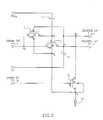
- FIG. 3illustrates a single stage of the source follower circuit of U.S. patent application Ser. No. 09/826,351.
- NMOS charge transfer transistor mhas its source connected to node n i ⁇ 1 , its gate connected to node g i , and its drain connected to node n i .
- Pulse train PHinjects energy into the pump through large capacitor 5 connected to node n i .
- Another pulse train PHAinjects energy into the pump through small capacitor 11 into node g i .
- An auxiliary transistor t ihas its drain connected to the gate node g i of charge transfer transistor m i .
- the source of auxiliary transistor t iis connected to the source of charge transfer transistor m i (i.e., node n i ⁇ 1 ).
- the gate of auxiliary transistor t iis connected to the drain of charge transfer transistor m i (i.e., node n i ).
- the auxiliary transistor t i and the PHAphase control the gate voltage of the charge transfer transistor m i .
- the P-well (PW) of the transistorsis isolated from the P-substrate, such as by a triple well process.
- An additional transistor s iis preferably configured as a source follower.
- a source followeris a method of configuring a FET, wherein the output voltage is at the source, and it “follows” the input voltage, which is connected to the gate. By “following” it is meant that the output voltage equals the input voltage minus the threshold voltage.
- the input of the source follower s iis from a previous pump stage and is used to drive the bulk of a subsequent pump stage.
- the gate of source follower s iis connected to the drain of charge transfer transistor m i ⁇ 2 .
- the source and bulk of source follower s iare connected to the bulk of charge transfer transistor m i and to the bulk of auxiliary transistor t i via a node p i and a node q i .
- Node p imay be connected to a bleeder element 12 , which may be, without limitation, a current source.
- the drain of source follower s iis connected to a high voltage, such as at a node w i , which may be the pump output or the stage output or input, for example
- the present inventionprovides a novel charge pump stage for pumping high positive voltages, which minimizes the abovementioned body effect.
- the methodmay boost the bulk voltage at any stage, even at the early pump stages.
- a method for operating a charge pumpcomprising providing a pulse train which injects energy into a charge pump stage to a gate of a charge transfer transistor of the charge pump stage, and inputting a modified output from the pulse train to a bulk of the charge transfer transistor such that a bulk voltage of the charge transfer transistor is raised to a level not greater than the minimum of a source voltage and a drain voltage of that charge transfer transistor.
- the bulk voltage of the charge pump stageis raised to a level below a minimum of source/drain voltages of a charge transfer transistor at that stage.
- modifying the outputcomprises connecting the pulse train to an input of a first inverter, which outputs to a second inverter, wherein an output of the second inverter is connected to the bulk of the charge transfer transistor.
- the methodcomprises providing an n-channel metal oxide semiconductor (NMOS) transistor, wherein a source of the NMOS transistor is connected to a positive supply of the second inverter, a gate of the NMOS transistor is connected to the drain of the charge transfer transistor, and a drain of the NMOS transistor is connected to a supply voltage (Vdd) of the charge pump stage.
- NMOSmetal oxide semiconductor
- the source voltage of the NMOS transistoris the minimum of Vdd and the difference between the voltage of the stage output and the threshold voltage of the NMOS transistor.
- the bulk of the NMOS transistoris connected to its source.
- a charge pump stagecomprising a pulse train which injects energy into a gate of a charge transfer transistor of the charge pump stage, wherein a modified output or the pulse train is input to a bulk of the charge transfer transistor such that a bulk voltage off the charge transfer transistor is raised to a level not greater than the minimum of a source voltage and a drain voltage of that charge transfer transistor.
- FIGS. 1 and 2are simplified circuit diagrams of a charge pump architecture commonly used in the prior art, comprising a threshold-voltage-canceling four-phased charge pump, wherein FIG. 1 illustrates four stages of the charge pump and FIG. 2 illustrated a single stage of the charge pump;
- FIG. 3is a simplified circuit diagram of a charge pump stage with a boosted well of the prior art, wherein the bulk of the stage is boosted by a source follower circuit;
- FIG. 4is a simplified circuit diagram of a charge pump stage with a boosted well, constructed and operative in accordance with an embodiment of the present invention.
- FIG. 5is a simplified graphical illustration of simulated waveforms for the charge pump stage of FIG. 4, in accordance with a preferred embodiment of the present invention.
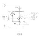
- FIG. 4illustrates a charge pump stage 20 with a boosted well, constructed and operative in accordance with an embodiment of the present invention.
- FIG. 4illustrates a single stage, but it is readily understood that the invention may comprise multiple stages connected to one another,
- NMOS charge transfer transistor m ihas its source connected to node n i ⁇ 1 , its gate connected to node g i , and its drain connected to node n i .
- Pulse train PHinjects energy into the pump through large capacitor 5 connected to node n i .
- Another pulse train PHAinjects energy into the pump through small capacitor 11 into node g i .
- An auxiliary transistor t ihas its drain connected to the gate node g i to charge transfer transistor m i .
- the source of auxiliary transistor t iis connected to the source of charge transfer transistor m i (i.e., node n i ⁇ 1 ).
- the gate of auxiliary transistor t iis connected to the drain of charge transfer transistor m i (i.e., node n i ).
- the auxiliary transistor t i and the PHA phase pulse traincontrol the gate voltage of the charge transfer transistor m i .
- the P-well (PW) of charge transfer transistor m i , as well as the PW of auxiliary transistor t i ,is preferably isolated from the P-substrate, which may be accomplished with triple-well technology.
- the P-wellmay be isolated from the P-substrate by an SOI structure, such as but not limited to, an SOS (silicon-on-sapphire) structure formed by heteroepitaxy of silicon on a monocrystalline sapphire substrate by CVD (chemical vapor deposition).
- SIMOXseparation by ion-implanted oxygen
- a silicon dioxide layeris formed by ion implantation of oxygen into a silicon monocrystalline substrate.
- charge pump stage 20may comprise an NMOS transistor N i , and inverters I 1 and I 2 .
- the drain of transistor N imay be connected to Vdd, which generally is the supply voltage to the particular charge pump stage.
- the source of transistor N imay be connected to the positive supply of inverter I 2 .
- the gate of transistor N imay be connected to the stage output, which for the single stage shown in FIG. 4, may be connected to the source of the charge transfer transistor m i+1 of the next stage.
- Pulse train PHAis connected to the input of inverter 11 . which outputs to inverter I 2 .
- the output of inverter I 2is connected to the bulk of charge transfer transistor m i . Accordingly, a modified output of pulse train PHA is input to the bulk of charge transfer transistor m i .
- the bulk of transistor N imay be optionally connected to its source.
- VsThe voltage at the source of transistor N i is designated as Vs.
- the pulse train PHAis high.
- the input to inverter I 2is a logic low, which means the output of inverter I 2 is driven to Vs.
- the output of inverter I 2is connected to the bulk of charge transfer transistor m i .
- the bulk of charge transfer transistor miis boosted to Vs, which is the minimum of Vdd and the difference between the voltage of the stage output and the threshold voltage (minimum of Vdd and V ni ⁇ V t ). This may significantly reduce the bulk effect of charge transfer transistor m i , and thus increase the efficiency of stage 20 .
- the bulk voltage at no pointcan exceed either the source or drain voltages of any charge transfer transistor m i , thus guaranteeing that no latchup or bipolar currents may be activated.
- the boosting mechanism of the present inventiondoes not depend on any outputs from prior stages, and may be applied to the all pump stages including the first pump stages.
- the additional components in the charge pump stagemay be of minimum size and thus may not occupy significant area or draw significant additional current.
- the gate of auxiliary transistor t imay be optionally connected to GND or to the PW of charge transfer transistor m i at node v i .
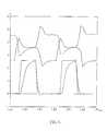
- FIG. 5illustrates simulated waveforms of the pump stage 20 of FIG. 4.
- FIG. 5illustrates voltage levels at the source side of charge transfer transistor m i (nodes n i ⁇ 1 in FIG. 4) and the drain side of charge transfer transistor m i (node n i in FIG. 4). It is noted that when comparing node n i ⁇ 1 to node n i , the average voltage of node n i is greater than that of node n i ⁇ 1 .
- transient period 15the well of charge transfer transistor m i may be boosted as described hereinabove, which results in a reduced bulk effect, and hence, more efficient charge transfer (node n 1 ⁇ 1 >node n i ).
- the voltage level of the bulk of each charge transfer transistor m iis raised to a level not greater than the minimum of the voltage level of the source and drain of that charge transfer transistor m i .
- the architecture of the present inventionensures that the P-well/bulk of each charge pump stage is raised to a level less than or equal to the minimum, during the entire clock cycle, of the source/drain voltage at that stage, which minimizes the bulk effect, and at the same time ensures that no diodes are forward biased.
Landscapes
- Engineering & Computer Science (AREA)
- Power Engineering (AREA)
- Dc-Dc Converters (AREA)
- Semiconductor Integrated Circuits (AREA)
Abstract
Description
- The present invention relates generally to charge pumps for boosting voltages in microelectronic circuitry, and particularly to a charge pump stage architecture with body effect minimization.[0001]
- Non-volatile memory arrays, such as erasable, programmable read only memory (EPROM) or flash memory arrays, or electrically erasable, programmable read only memory (EEPROM) arrays, require high positive or negative voltages to program and erase memory cells of the array. Typically, these voltages are higher than the voltage supplied (Vdd). Charge pumps are generally used to boost on-chip voltages above the supply voltage Vdd to reach the voltages required for programming or erasing.[0002]
- A charge pump typically comprises cascaded stages that progressively boost the voltage to higher levels. The charge pump functions by progressively storing more charge on a capacitor which is part of a capacitor-diode combination, with several such stages being placed together in a network to obtain the desired increase in voltage. The diode functions to prevent discharge of the capacitor prior to placing the additional charge thereon.[0003]
- Reference is now made to FIGS. 1 and 2, which respectively illustrate four stages and a single stage of a commonly used charge pump architecture, called a four-phased-clock, threshold-voltage-canceling pump architecture, for a four-stage charge pump (see Umezawa, IEEE Journal of Solid State Circuits, Vol. 27, 1992, page 1540).[0004]
- The charge pump circuit includes a plurality of charge transfer transistors (reference letters m[0005]i) connected in series. In FIG. 1, four such charge transfer transistors are shown, labeled m1, m2, m3and m4. In FIG. 2, which shows a single stage, one charge transfer transistor miis shown. Charge transfer transistors mimay use, but are not limited to, CMOS (complementary metal oxide semiconductor) technology, being either n-channel or p-channel (NMOS or PMOS) field effect transistors (FETs). FIGS. 1 and 2 illustrate a positive charge pump based on NMOS. It is noted that NMOS is generally used to pump positive voltages, whereas PMOS is generally used to pump negative voltages. The charge transfer transistors have a control electrode (gate, labeled g), a first electrode (drain, labeled d) and a second electrode (source, labeled s), connected to nodes, as described hereinbelow. (Since MOSFETs are typically symmetrical components, the true designation of “source” and “drain” is only possible once a voltage is impressed on the terminals of the transistors. The designations of source and drain throughout the specification should be interpreted, therefore, in the broadest sense.) Preferably, the bulks (labeled b) of the charge transfer transistors miare coupled to a reference line REF (FIG. 2) for receiving a reference voltage, generally ground in the case of NMOS.
- Referring to FIG. 1, the source of charge transfer transistor m[0006]1is connected to node n0, which is connected to Vdd. The gate of charge transfer transistor m1is connected to node g1, and the drain is connected to node n1. (In the general single stage shown in FIG. 2, the source of charge transfer transistor mi is connected to node ni−1the gate is connected to node gi, and the drain is connected to node ni.) The source of charge transfer transistor m2is connected to node n1, the gate is connected to node g2, and the drain is connected to node n2. Similarly, the source of charge transfer transistor m3is connected to node n2, the gate to node g3, and the drain to node n3. Likewise, the source of charge transfer transistor m4is connected to node n3, the gate to node g4, and the drain to node n4.
- Two-phase pulse trains PH[0007]1 and PH2, and PH1A and PH2A are provided (FIG. 1), such as from a pulse generator (not shown). The PH1 and PH1A phases may be non-overlapping with respect to each other, and the PH2 and PH2A phases may be non-overlapping with respect to each other. The PH1 and PH2 phase may be overlapping. By non-overlapping it is meant that 0 to 1, and 1 to 0 voltage transitions of one pulse never overlap with the transitions of the other pulse. The PH1 and PH2 phases inject energy into the pump through
large capacitors 5 into nodes ni. Accordingly, in the illustrated embodiment, alarge capacitor 5 is connected from pulse train PH1 to node n1, and anotherlarge capacitor 5 is connected from pulse train PH1 to node n3. Anotherlarge capacitor 5 is connected from pulse train PH2 to node n2, and anotherlarge capacitor 5 is connected from pulse train PH2 to node n4. The charge is transferred along the pump through charge transfer transistors miconnecting node nito node ni+1. (In the general single stage shown in FIG. 2,large capacitor 5 is connected from pulse train PH to node ni.) - The PH[0008]1A and PH2A phases inject energy into the pump through
small capacitors 11 into nodes gi.Capacitors 11 preferably have a much smaller capacitance thanlarge capacitors 5. In the illustrated embodiment asmall capacitor 11 is connected from pulse train PH1A to node g2, and anothersmall capacitor 11 is connected from pulse train PH1A to node g4. Anothersmall capacitor 11 is connected from pulse train PH2A to node g1, and anothersmall capacitor 11 is connected from pulse train PH2A to node g3. (In the general single stage shown in FIG. 2,small capacitor 11 is connected from pulse train PHA to node gi.) - As seen in FIGS. 1, a plurality of auxiliary transistors t[0009]i(i.e., t1, t2, t3and t4) are provided. In FIG. 2, which shows a single stage, one auxiliary Transistor tiis shown. Each auxiliary transistor tihas its drain connected to the gate node giof each charge transfer transistor mi(i.e., m1, m2, m3and m4, respectively, in FIG. 1). The source of each auxiliary transistor tiis connected to the source of each charge transfer transistor mi(i.e., node ni−1). The gate of each auxiliary transistor tiis connected to the drain of each charge transfer transistor mi(i.e., node ni). The bulk of each auxiliary transistor tiis connected to the bulk of each charge transfer transistor mi, which is generally grounded. The auxiliary transistors tiand the PH1A and PH2A phases (PHA in the single stage shown in FIG. 2) and
small capacitors 11 may control the gate voltage of the charge transfer transistors mi. - The operation of the first stage of the pump is now explained, with all subsequent stages operating in the same manner. The operation commences with the PH[0010]1 phase starting to rise. Initially, charge transfer transistors m1and m2are non-conducting (i.e., turned off), since the PH1A and PH2A phases arc in their low phase. The PH1 phase then fully rises and injects energy into node n1, raising (or “pushing”) node n1to a voltage boosted above Vdd, such as 2 Vdd. The rise of node n1forces node g1to Vdd through auxiliary transistor t1. Since the source of charge transfer transistor m1is connected to Vdd at node no, the gate-source voltage bias Vgsof charge transfer transistor m1is zero, assuring that transistor m1is turned off.
- After a short time, typically in the order of several nanoseconds, the PH[0011]1A phase rises, which makes charge transfer transistor m2conduct (i.e., turns on). During this time, node n1is at a higher voltage than node n2. Since, as just mentioned, charge transfer transistor m2is conducting, charge is transferred from node n1to node n2. During the next phase, the PH2 phase rises and the PH1 phase drops. This causes node n1to drop and node n2to rise, thereby causing charge to be transferred from node n2to node n3. In this manner charge is transferred along the pump. Each of the ginodes is raised by a Vdd level with respect to the ninodes when charge transfer is taking place. In the latter stages of the pump, the source and drain nodes (i.e., nodes n3and n4) are raised well above the bulk, which is usually grounded.
- In the more general case of a single stage, shown in FIG. 2, the charge is injected into the stage when the PH signal of the previous stage is high, and is transferred across the charge transfer transistor m[0012]iwhen the PHA signal is high. Note that when comparing node n−1to ni, the average voltage of niis greater than that of ni−1. However, during the stage when charge is transferred from n1−1to ni, the voltage of ni−1is briefly higher than that of ni.
- The large voltage difference between the high source/drain voltages and the low bulk voltage causes a problem, called the body or bulk effect, which is now explained. (The terms body and bulk are used interchangeably throughout the specification and claims.)[0013]
- Positive charge pumps generally use NMOS transistors, and this requires the body of the charge transfer transistors to be at the lowest voltage, in general ground (GND). (Negative charge pumps have the opposite requirement, and PMOS transistors are generally used.) However, in positive charge pumps there can be a significant loss of energy in the latter pump stages due to the “body effect”. In NMOS, the body effect causes an increase in the threshold voltage (V[0014]t), due to the fact that the bulk or body of the transistor is at a lower voltage than the source. Due to the body effect, the threshold voltage Vtof the NMOS transistors progressively increases from the stages near the input terminal of the charge pump to the stages near the output terminal. For example, in the prior art charge pump of FIG. 1, the threshold voltage Vtof charge transfer transistors miprogressively increases from transistor mito transistor m4. In transistor m4, as mentioned hereinabove, the source and drain nodes n3and n4, have been raised well above the bulk. This reduces the efficiency of the charge pump, because the charge transfer through each stage decreases.
- In some CMOS processes, such as triple-well and silicon-on-insulator (SOI), it is possible to raise the bulk of the NMOS charge transfer transistors above the grounded substrate, which would reduce the body effect by diminishing the voltage difference between the bulk and the source/drain. However, in the prior art, this entails certain risks. For example, if the bulk voltage is raised above the source or drain voltage, then parasitic bipolar transistors (typically found in CMOS processes) can turn on, which can cause either latchup or drain the charge from the pump.[0015]
- In many circuits, not necessarily charge pumps, the bulk effect is eliminated by connecting the bulk node to the source node. This is not possible in a charge pump, however, because the “source” can be higher or lower than the “drain” by Vdd, depending upon the clock cycle. This would cause parasitic diodes to turn on, resulting in the unwanted bipolar transistor turn-on and latchup.[0016]
- One method for compensating for the body effect is described in U.S. Pat. No. 6,064,251 to Park. Park uses charge pump stages coupled in series. Each charge pump is stage has two clock terminals that receive two phase shifted clock signals. The charge pump stages are configured so that adjacent charge pump stages receive different clock signals. The phases of the clock signals arc such that the pump elements are boosted well above the threshold voltage V[0017]t, thereby providing the transistors with sufficient overdrive to transfer energy along the pump. However, clock boosting uses a significant amount of power consumption and is thus very inefficient.
- Another prior attempt to minimize the bulk effect is described in U.S. patent application Ser. No. 09/826,351, assigned to the same assignee of the present invention, the disclosure of which is incorporated herein by reference. This method is effective in the latter pump stages (from the fourth stage onwards). In this case, the bulk of the stage is boosted by a source follower circuit whose gate is connected to the output of a previous stage at a voltage V, boosting the bulk to V-V[0018]t, where Vtis the threshold voltage of the source follower.
- FIG. 3 illustrates a single stage of the source follower circuit of U.S. patent application Ser. No. 09/826,351. NMOS charge transfer transistor m; has its source connected to node n[0019]i−1, its gate connected to node gi, and its drain connected to node ni. Pulse train PH injects energy into the pump through
large capacitor 5 connected to node ni. Another pulse train PHA injects energy into the pump throughsmall capacitor 11 into node gi. - An auxiliary transistor t[0020]ihas its drain connected to the gate node giof charge transfer transistor mi. The source of auxiliary transistor tiis connected to the source of charge transfer transistor mi(i.e., node ni−1). The gate of auxiliary transistor tiis connected to the drain of charge transfer transistor mi(i.e., node ni). The auxiliary transistor tiand the PHA phase control the gate voltage of the charge transfer transistor mi. The P-well (PW) of the transistors is isolated from the P-substrate, such as by a triple well process.
- An additional transistor s[0021]iis preferably configured as a source follower. A source follower is a method of configuring a FET, wherein the output voltage is at the source, and it “follows” the input voltage, which is connected to the gate. By “following” it is meant that the output voltage equals the input voltage minus the threshold voltage. The input of the source follower siis from a previous pump stage and is used to drive the bulk of a subsequent pump stage.
- In the circuitry of FIG. 3, the gate of source follower s[0022]iis connected to the drain of charge transfer transistor mi−2. The source and bulk of source follower siare connected to the bulk of charge transfer transistor miand to the bulk of auxiliary transistor tivia a node piand a node qi. Node pimay be connected to a
bleeder element 12, which may be, without limitation, a current source. The drain of source follower siis connected to a high voltage, such as at a node wi, which may be the pump output or the stage output or input, for example - The disadvantage of this method is that it only provides a solution for the latter pump stages. In the earlier stages, there is also a significant bulk effect, which can deteriorate the pump's efficiency. There is accordingly a need for a method to efficiently compensate for the bulk effect in the early pump stages, without opening the parasitic bipolar transistors.[0023]
- The present invention provides a novel charge pump stage for pumping high positive voltages, which minimizes the abovementioned body effect. In the present invention, the method may boost the bulk voltage at any stage, even at the early pump stages.[0024]
- There is thus provided hi accordance with an embodiment of the present invention a method for operating a charge pump, the method comprising providing a pulse train which injects energy into a charge pump stage to a gate of a charge transfer transistor of the charge pump stage, and inputting a modified output from the pulse train to a bulk of the charge transfer transistor such that a bulk voltage of the charge transfer transistor is raised to a level not greater than the minimum of a source voltage and a drain voltage of that charge transfer transistor.[0025]
- In accordance with an embodiment of the present invention the bulk voltage of the charge pump stage is raised to a level below a minimum of source/drain voltages of a charge transfer transistor at that stage.[0026]
- Further in accordance with an embodiment of the present invention modifying the output comprises connecting the pulse train to an input of a first inverter, which outputs to a second inverter, wherein an output of the second inverter is connected to the bulk of the charge transfer transistor.[0027]
- Still further in accordance with an embodiment of the present invention the method comprises providing an n-channel metal oxide semiconductor (NMOS) transistor, wherein a source of the NMOS transistor is connected to a positive supply of the second inverter, a gate of the NMOS transistor is connected to the drain of the charge transfer transistor, and a drain of the NMOS transistor is connected to a supply voltage (Vdd) of the charge pump stage.[0028]
- In accordance with an embodiment of the present invention the source voltage of the NMOS transistor (Vs) is the minimum of Vdd and the difference between the voltage of the stage output and the threshold voltage of the NMOS transistor.[0029]
- Further in accordance with an embodiment of the present invention the bulk of the NMOS transistor is connected to its source.[0030]
- There is also provided in accordance with an embodiment of the present invention a charge pump stage comprising a pulse train which injects energy into a gate of a charge transfer transistor of the charge pump stage, wherein a modified output or the pulse train is input to a bulk of the charge transfer transistor such that a bulk voltage off the charge transfer transistor is raised to a level not greater than the minimum of a source voltage and a drain voltage of that charge transfer transistor.[0031]
- The present invention will be understood and appreciated more fully from the following detailed description taken in conjunction with the drawings in which:[0032]
- FIGS. 1 and 2 are simplified circuit diagrams of a charge pump architecture commonly used in the prior art, comprising a threshold-voltage-canceling four-phased charge pump, wherein FIG. 1 illustrates four stages of the charge pump and FIG. 2 illustrated a single stage of the charge pump;[0033]
- FIG. 3 is a simplified circuit diagram of a charge pump stage with a boosted well of the prior art, wherein the bulk of the stage is boosted by a source follower circuit;[0034]
- In FIG. 4 is a simplified circuit diagram of a charge pump stage with a boosted well, constructed and operative in accordance with an embodiment of the present invention; and[0035]
- FIG. 5 is a simplified graphical illustration of simulated waveforms for the charge pump stage of FIG. 4, in accordance with a preferred embodiment of the present invention.[0036]
- Reference is now made to FIG. 4, which illustrates a[0037]
charge pump stage 20 with a boosted well, constructed and operative in accordance with an embodiment of the present invention. FIG. 4 illustrates a single stage, but it is readily understood that the invention may comprise multiple stages connected to one another, - In[0038]
charge pump stage 20, NMOS charge transfer transistor mihas its source connected to node ni−1, its gate connected to node gi, and its drain connected to node ni. Pulse train PH injects energy into the pump throughlarge capacitor 5 connected to node ni. Another pulse train PHA injects energy into the pump throughsmall capacitor 11 into node gi. - An auxiliary transistor t[0039]ihas its drain connected to the gate node gito charge transfer transistor mi. The source of auxiliary transistor tiis connected to the source of charge transfer transistor mi(i.e., node ni−1). The gate of auxiliary transistor tiis connected to the drain of charge transfer transistor mi(i.e., node ni). The auxiliary transistor tiand the PHA phase pulse train control the gate voltage of the charge transfer transistor mi.
- The P-well (PW) of charge transfer transistor m[0040]i, as well as the PW of auxiliary transistor ti, is preferably isolated from the P-substrate, which may be accomplished with triple-well technology. However, other transistor;architectures may be used to carry out the invention other than triple-well technology. For example, the P-well may be isolated from the P-substrate by an SOI structure, such as but not limited to, an SOS (silicon-on-sapphire) structure formed by heteroepitaxy of silicon on a monocrystalline sapphire substrate by CVD (chemical vapor deposition). Another example is that of SIMOX (separation by ion-implanted oxygen) in which a silicon dioxide layer is formed by ion implantation of oxygen into a silicon monocrystalline substrate.
- In accordance with an embodiment or the invention,[0041]
charge pump stage 20 may comprise an NMOS transistor Ni, and inverters I1 and I2. The drain of transistor Nimay be connected to Vdd, which generally is the supply voltage to the particular charge pump stage. The source of transistor Nimay be connected to the positive supply of inverter I2. The gate of transistor Nimay be connected to the stage output, which for the single stage shown in FIG. 4, may be connected to the source of the charge transfer transistor mi+1of the next stage. Pulse train PHA is connected to the input ofinverter 11. which outputs to inverter I2. The output of inverter I2 is connected to the bulk of charge transfer transistor mi. Accordingly, a modified output of pulse train PHA is input to the bulk of charge transfer transistor mi. The bulk of transistor Nimay be optionally connected to its source. - The voltage at the source of transistor N[0042]iis designated as Vs. Vs is the minimum of Vdd (the positive rail) and the difference between the voltage of the stage output (tile drain of the charge transfer transistor miof the present stage at node ni, which leads to the source of the charge transfer transistor mi+1, of the next stage) and the threshold voltage (Vt) of the charge transfer transistor miof the present stage. Accordingly, in the preceding nomenclature, Vs=MIN (Vdd, Vni−Vt).
- As mentioned hereinabove, during the charge transfer stage the pulse train PHA is high. Alter inversion by inverter I[0043]1, the input to inverter I2 is a logic low, which means the output of inverter I2 is driven to Vs. As mentioned previously, the output of inverter I2 is connected to the bulk of charge transfer transistor mi. Thus, during the charge transfer stage, the bulk of charge transfer transistor mi is boosted to Vs, which is the minimum of Vdd and the difference between the voltage of the stage output and the threshold voltage (minimum of Vdd and Vni−Vt). This may significantly reduce the bulk effect of charge transfer transistor mi, and thus increase the efficiency of
stage 20. The bulk voltage at no point can exceed either the source or drain voltages of any charge transfer transistor mi, thus guaranteeing that no latchup or bipolar currents may be activated. Unlike the prior art, the boosting mechanism of the present invention does not depend on any outputs from prior stages, and may be applied to the all pump stages including the first pump stages. The additional components in the charge pump stage (transistor Ni, and inverters I1 and I2) may be of minimum size and thus may not occupy significant area or draw significant additional current. The gate of auxiliary transistor timay be optionally connected to GND or to the PW of charge transfer transistor miat node vi. - Reference is now made to FIG. 5, which illustrates simulated waveforms of the[0044]
pump stage 20 of FIG. 4. FIG. 5 illustrates voltage levels at the source side of charge transfer transistor mi(nodes ni−1in FIG. 4) and the drain side of charge transfer transistor mi(node niin FIG. 4). It is noted that when comparing node ni−1to node ni, the average voltage of node niis greater than that of node ni−1. However, during the charge transfer phase, when PHA is high and charge is transferred from node ni−1to node ni, the voltage of node ni−1is briefly higher than that of node nifor a short transient period, such transient periods being designated byreference numeral 15 in FIG. 5. Duringtransient period 15, the well of charge transfer transistor mimay be boosted as described hereinabove, which results in a reduced bulk effect, and hence, more efficient charge transfer (node n1−1>node ni). - Accordingly, the voltage level of the bulk of each charge transfer transistor m[0045]iis raised to a level not greater than the minimum of the voltage level of the source and drain of that charge transfer transistor mi. The architecture of the present invention ensures that the P-well/bulk of each charge pump stage is raised to a level less than or equal to the minimum, during the entire clock cycle, of the source/drain voltage at that stage, which minimizes the bulk effect, and at the same time ensures that no diodes are forward biased.
- It will be appreciated by person skilled in the art, that the present invention is not limited by what has been particularly shown and described herein above. Rather the scope of the present invention is defined only by the claims which follow:[0046]
Claims (11)
Priority Applications (1)
| Application Number | Priority Date | Filing Date | Title |
|---|---|---|---|
| US10/322,491US7148739B2 (en) | 2002-12-19 | 2002-12-19 | Charge pump element with body effect cancellation for early charge pump stages |
Applications Claiming Priority (1)
| Application Number | Priority Date | Filing Date | Title |
|---|---|---|---|
| US10/322,491US7148739B2 (en) | 2002-12-19 | 2002-12-19 | Charge pump element with body effect cancellation for early charge pump stages |
Publications (2)
| Publication Number | Publication Date |
|---|---|
| US20040119525A1true US20040119525A1 (en) | 2004-06-24 |
| US7148739B2 US7148739B2 (en) | 2006-12-12 |
Family
ID=32592999
Family Applications (1)
| Application Number | Title | Priority Date | Filing Date |
|---|---|---|---|
| US10/322,491Expired - LifetimeUS7148739B2 (en) | 2002-12-19 | 2002-12-19 | Charge pump element with body effect cancellation for early charge pump stages |
Country Status (1)
| Country | Link |
|---|---|
| US (1) | US7148739B2 (en) |
Cited By (1)
| Publication number | Priority date | Publication date | Assignee | Title |
|---|---|---|---|---|
| US20040054514A1 (en)* | 2002-05-30 | 2004-03-18 | Stmicroelectronics Sa | Method and device for characterizing a CMOS logic cell to be produced in a technology of the partially depleted silicon-on-insulator type |
Families Citing this family (1)
| Publication number | Priority date | Publication date | Assignee | Title |
|---|---|---|---|---|
| EP3579233B1 (en)* | 2018-06-04 | 2021-01-27 | EM Microelectronic-Marin SA | Basic cell and priming pumps comprising such a basic cell |
Citations (21)
| Publication number | Priority date | Publication date | Assignee | Title |
|---|---|---|---|---|
| US5029063A (en)* | 1989-03-25 | 1991-07-02 | Eurosil Electronic Gmbh | MOSFET multiplying circuit |
| US5081371A (en)* | 1990-11-07 | 1992-01-14 | U.S. Philips Corp. | Integrated charge pump circuit with back bias voltage reduction |
| US5636288A (en)* | 1995-02-16 | 1997-06-03 | Paradigm Electronics Inc. | Standby power circuit arrangement |
| US5717581A (en)* | 1994-06-30 | 1998-02-10 | Sgs-Thomson Microelectronics, Inc. | Charge pump circuit with feedback control |
| US5726946A (en)* | 1994-06-02 | 1998-03-10 | Mitsubishi Denki Kabushiki Kaisha | Semiconductor integrated circuit device having hierarchical power source arrangement |
| US5847441A (en)* | 1996-05-10 | 1998-12-08 | Micron Technology, Inc. | Semiconductor junction antifuse circuit |
| US5880620A (en)* | 1997-04-22 | 1999-03-09 | Xilinx, Inc. | Pass gate circuit with body bias control |
| US5903031A (en)* | 1995-07-04 | 1999-05-11 | Matsushita Electric Industrial Co., Ltd. | MIS device, method of manufacturing the same, and method of diagnosing the same |
| US5963412A (en)* | 1997-11-13 | 1999-10-05 | Advanced Micro Devices, Inc. | Process induced charging damage control device |
| US6028324A (en)* | 1997-03-07 | 2000-02-22 | Taiwan Semiconductor Manufacturing Company | Test structures for monitoring gate oxide defect densities and the plasma antenna effect |
| US6064251A (en)* | 1997-08-27 | 2000-05-16 | Integrated Silicon Solution, Inc. | System and method for a low voltage charge pump with large output voltage range |
| US6081456A (en)* | 1999-02-04 | 2000-06-27 | Tower Semiconductor Ltd. | Bit line control circuit for a memory array using 2-bit non-volatile memory cells |
| US6130574A (en)* | 1997-01-24 | 2000-10-10 | Siemens Aktiengesellschaft | Circuit configuration for producing negative voltages, charge pump having at least two circuit configurations and method of operating a charge pump |
| US6198342B1 (en)* | 1998-12-08 | 2001-03-06 | Sharp Kabushiki Kaisha | Charge pump circuit simple in construction and free from trouble even at low voltage |
| US6208200B1 (en)* | 1997-07-14 | 2001-03-27 | Sony Corporation | Level shift circuit with low voltage operation |
| US6297974B1 (en)* | 1999-09-27 | 2001-10-02 | Intel Corporation | Method and apparatus for reducing stress across capacitors used in integrated circuits |
| US6353356B1 (en)* | 1999-08-30 | 2002-03-05 | Micron Technology, Inc. | High voltage charge pump circuits |
| US6359501B2 (en)* | 2000-02-11 | 2002-03-19 | Windbond Eelctronics Corp. | Charge-pumping circuits for a low-supply voltage |
| US6400209B1 (en)* | 1999-08-05 | 2002-06-04 | Fujitsu Limited | Switch circuit with back gate voltage control and series regulator |
| US6452438B1 (en)* | 2000-12-28 | 2002-09-17 | Intel Corporation | Triple well no body effect negative charge pump |
| US20020145464A1 (en)* | 2001-04-05 | 2002-10-10 | Shor Joseph S. | Charge pump stage with body effect minimization |
Family Cites Families (1)
| Publication number | Priority date | Publication date | Assignee | Title |
|---|---|---|---|---|
| EP0693781B1 (en) | 1994-07-13 | 2002-10-02 | United Microelectronics Corporation | Grounding method for eliminating process antenna effect |
- 2002
- 2002-12-19USUS10/322,491patent/US7148739B2/ennot_activeExpired - Lifetime
Patent Citations (21)
| Publication number | Priority date | Publication date | Assignee | Title |
|---|---|---|---|---|
| US5029063A (en)* | 1989-03-25 | 1991-07-02 | Eurosil Electronic Gmbh | MOSFET multiplying circuit |
| US5081371A (en)* | 1990-11-07 | 1992-01-14 | U.S. Philips Corp. | Integrated charge pump circuit with back bias voltage reduction |
| US5726946A (en)* | 1994-06-02 | 1998-03-10 | Mitsubishi Denki Kabushiki Kaisha | Semiconductor integrated circuit device having hierarchical power source arrangement |
| US5717581A (en)* | 1994-06-30 | 1998-02-10 | Sgs-Thomson Microelectronics, Inc. | Charge pump circuit with feedback control |
| US5636288A (en)* | 1995-02-16 | 1997-06-03 | Paradigm Electronics Inc. | Standby power circuit arrangement |
| US5903031A (en)* | 1995-07-04 | 1999-05-11 | Matsushita Electric Industrial Co., Ltd. | MIS device, method of manufacturing the same, and method of diagnosing the same |
| US5847441A (en)* | 1996-05-10 | 1998-12-08 | Micron Technology, Inc. | Semiconductor junction antifuse circuit |
| US6130574A (en)* | 1997-01-24 | 2000-10-10 | Siemens Aktiengesellschaft | Circuit configuration for producing negative voltages, charge pump having at least two circuit configurations and method of operating a charge pump |
| US6028324A (en)* | 1997-03-07 | 2000-02-22 | Taiwan Semiconductor Manufacturing Company | Test structures for monitoring gate oxide defect densities and the plasma antenna effect |
| US5880620A (en)* | 1997-04-22 | 1999-03-09 | Xilinx, Inc. | Pass gate circuit with body bias control |
| US6208200B1 (en)* | 1997-07-14 | 2001-03-27 | Sony Corporation | Level shift circuit with low voltage operation |
| US6064251A (en)* | 1997-08-27 | 2000-05-16 | Integrated Silicon Solution, Inc. | System and method for a low voltage charge pump with large output voltage range |
| US5963412A (en)* | 1997-11-13 | 1999-10-05 | Advanced Micro Devices, Inc. | Process induced charging damage control device |
| US6198342B1 (en)* | 1998-12-08 | 2001-03-06 | Sharp Kabushiki Kaisha | Charge pump circuit simple in construction and free from trouble even at low voltage |
| US6081456A (en)* | 1999-02-04 | 2000-06-27 | Tower Semiconductor Ltd. | Bit line control circuit for a memory array using 2-bit non-volatile memory cells |
| US6400209B1 (en)* | 1999-08-05 | 2002-06-04 | Fujitsu Limited | Switch circuit with back gate voltage control and series regulator |
| US6353356B1 (en)* | 1999-08-30 | 2002-03-05 | Micron Technology, Inc. | High voltage charge pump circuits |
| US6297974B1 (en)* | 1999-09-27 | 2001-10-02 | Intel Corporation | Method and apparatus for reducing stress across capacitors used in integrated circuits |
| US6359501B2 (en)* | 2000-02-11 | 2002-03-19 | Windbond Eelctronics Corp. | Charge-pumping circuits for a low-supply voltage |
| US6452438B1 (en)* | 2000-12-28 | 2002-09-17 | Intel Corporation | Triple well no body effect negative charge pump |
| US20020145464A1 (en)* | 2001-04-05 | 2002-10-10 | Shor Joseph S. | Charge pump stage with body effect minimization |
Cited By (2)
| Publication number | Priority date | Publication date | Assignee | Title |
|---|---|---|---|---|
| US20040054514A1 (en)* | 2002-05-30 | 2004-03-18 | Stmicroelectronics Sa | Method and device for characterizing a CMOS logic cell to be produced in a technology of the partially depleted silicon-on-insulator type |
| US6871330B2 (en)* | 2002-05-30 | 2005-03-22 | Stmicroelectronics Sa | Method and device for characterizing a CMOS logic cell to be produced in a technology of the partially depleted silicon-on-insulator type |
Also Published As
| Publication number | Publication date |
|---|---|
| US7148739B2 (en) | 2006-12-12 |
Similar Documents
| Publication | Publication Date | Title |
|---|---|---|
| US6677805B2 (en) | Charge pump stage with body effect minimization | |
| US6130572A (en) | NMOS negative charge pump | |
| US6661682B2 (en) | High voltage generating charge pump circuit | |
| US6914791B1 (en) | High efficiency triple well charge pump circuit | |
| US6418040B1 (en) | Bi-directional architecture for a high-voltage cross-coupled charge pump | |
| US6501325B1 (en) | Low voltage supply higher efficiency cross-coupled high voltage charge pumps | |
| US6538930B2 (en) | Charge pump circuit for generating positive and negative voltage with reverse current prevention circuit and a nonvolatile memory using the same | |
| US6819162B2 (en) | Charge pump for negative voltages | |
| US7728652B2 (en) | Semiconductor integrated circuit | |
| EP0485016B1 (en) | Integrated charge pump circuit with back bias voltage reduction | |
| EP0843402B1 (en) | BiCMOS negative charge pump | |
| US5347171A (en) | Efficient negative charge pump | |
| US6747897B2 (en) | Semiconductor charge pump circuit and nonvolatile semiconductor memory device | |
| US20050146375A1 (en) | Charge pump circuit suitable for low-voltage process | |
| US6198340B1 (en) | High efficiency CMOS pump circuit | |
| US5994949A (en) | Negative voltage charge pump particularly for flash EEPROM memories | |
| US7652522B2 (en) | High efficiency low cost bi-directional charge pump circuit for very low voltage applications | |
| US6356137B1 (en) | Voltage boost circuit with low power supply voltage | |
| JPH06261538A (en) | High-voltage charge pump | |
| US5412257A (en) | High efficiency N-channel charge pump having a primary pump and a non-cascaded secondary pump | |
| US7256438B2 (en) | MOS capacitor with reduced parasitic capacitance | |
| RU2137294C1 (en) | High-voltage turn-on mos device built around semiconductor integrated circuit | |
| Min et al. | CMOS charge pumps using cross-coupled charge transfer switches with improved voltage pumping gain and low gate-oxide stress for low-voltage memory circuits | |
| US20050088220A1 (en) | Charge pump circuit having high charge transfer efficiency | |
| US20240372543A1 (en) | MULTIPHASE N-CHANNEL HIGH-SIDE SWITCH FOR GaN INTEGRATED CIRCUITS |
Legal Events
| Date | Code | Title | Description |
|---|---|---|---|
| STCF | Information on status: patent grant | Free format text:PATENTED CASE | |
| REMI | Maintenance fee reminder mailed | ||
| FPAY | Fee payment | Year of fee payment:4 | |
| SULP | Surcharge for late payment | ||
| FPAY | Fee payment | Year of fee payment:8 | |
| AS | Assignment | Owner name:MORGAN STANLEY SENIOR FUNDING, INC., NEW YORK Free format text:SECURITY INTEREST;ASSIGNOR:CYPRESS SEMICONDUCTOR CORPORATION;REEL/FRAME:039676/0237 Effective date:20160805 | |
| MAFP | Maintenance fee payment | Free format text:PAYMENT OF MAINTENANCE FEE, 12TH YEAR, LARGE ENTITY (ORIGINAL EVENT CODE: M1553) Year of fee payment:12 | |
| AS | Assignment | Owner name:MORGAN STANLEY SENIOR FUNDING, NEW YORK Free format text:CORRECTIVE ASSIGNMENT TO CORRECT THE FOLLOWING NUMBERS 6272046,7277824,7282374,7286384,7299106,7337032,7460920,7519447 PREVIOUSLY RECORDED ON REEL 039676 FRAME 0237. ASSIGNOR(S) HEREBY CONFIRMS THE SECURITY INTEREST;ASSIGNOR:CYPRESS SEMICONDUCTOR CORPORATION;REEL/FRAME:047797/0854 Effective date:20171229 | |
| AS | Assignment | Owner name:SPANSION LLC, CALIFORNIA Free format text:RELEASE BY SECURED PARTY;ASSIGNOR:MUFG UNION BANK, N.A.;REEL/FRAME:059410/0438 Effective date:20200416 Owner name:CYPRESS SEMICONDUCTOR CORPORATION, CALIFORNIA Free format text:RELEASE BY SECURED PARTY;ASSIGNOR:MUFG UNION BANK, N.A.;REEL/FRAME:059410/0438 Effective date:20200416 |