US20040119097A1 - Integrated chip package structure using organic substrate and method of manufacturing the same - Google Patents
Integrated chip package structure using organic substrate and method of manufacturing the sameDownload PDFInfo
- Publication number
- US20040119097A1 US20040119097A1US10/728,150US72815003AUS2004119097A1US 20040119097 A1US20040119097 A1US 20040119097A1US 72815003 AUS72815003 AUS 72815003AUS 2004119097 A1US2004119097 A1US 2004119097A1
- Authority
- US
- United States
- Prior art keywords
- layer
- patterned wiring
- wiring layer
- die
- allocating
- Prior art date
- Legal status (The legal status is an assumption and is not a legal conclusion. Google has not performed a legal analysis and makes no representation as to the accuracy of the status listed.)
- Granted
Links
- 239000000758substrateSubstances0.000titleclaimsabstractdescription203
- 238000004519manufacturing processMethods0.000titleclaimsabstractdescription25
- 239000002184metalSubstances0.000claimsabstractdescription74
- 229910052751metalInorganic materials0.000claimsabstractdescription74
- 239000010409thin filmSubstances0.000claimsabstractdescription54
- 239000010410layerSubstances0.000claimsdescription489
- 238000000034methodMethods0.000claimsdescription151
- 238000011049fillingMethods0.000claimsdescription67
- 239000012044organic layerSubstances0.000claimsdescription41
- 239000000463materialSubstances0.000claimsdescription39
- 239000004020conductorSubstances0.000claimsdescription24
- 238000002161passivationMethods0.000claimsdescription18
- 229910000679solderInorganic materials0.000claimsdescription18
- 239000004642PolyimideSubstances0.000claimsdescription12
- UMIVXZPTRXBADB-UHFFFAOYSA-NbenzocyclobuteneChemical compoundC1=CC=C2CCC2=C1UMIVXZPTRXBADB-UHFFFAOYSA-N0.000claimsdescription12
- 239000003989dielectric materialSubstances0.000claimsdescription11
- 238000004806packaging method and processMethods0.000claimsdescription10
- 239000004593EpoxySubstances0.000claimsdescription9
- 239000003990capacitorSubstances0.000claimsdescription9
- 230000002093peripheral effectEffects0.000claimsdescription8
- 229920000642polymerPolymers0.000claimsdescription8
- 238000007772electroless platingMethods0.000claimsdescription7
- 238000009713electroplatingMethods0.000claimsdescription7
- 238000004377microelectronicMethods0.000claimsdescription7
- 238000000059patterningMethods0.000claimsdescription7
- 238000004544sputter depositionMethods0.000claimsdescription7
- 238000001746injection mouldingMethods0.000claimsdescription6
- 239000011368organic materialSubstances0.000claimsdescription6
- 239000011521glassSubstances0.000claimsdescription4
- -1organicSubstances0.000claimsdescription3
- 229920001721polyimidePolymers0.000claims10
- 239000002344surface layerSubstances0.000claims3
- 238000010586diagramMethods0.000description21
- 230000015572biosynthetic processEffects0.000description18
- 238000000227grindingMethods0.000description5
- 239000011810insulating materialSubstances0.000description5
- 238000003825pressingMethods0.000description4
- 239000002356single layerSubstances0.000description4
- 230000008901benefitEffects0.000description3
- 238000005516engineering processMethods0.000description3
- 239000010949copperSubstances0.000description2
- 238000001723curingMethods0.000description2
- 230000000694effectsEffects0.000description2
- 238000005530etchingMethods0.000description2
- 230000010354integrationEffects0.000description2
- 238000012986modificationMethods0.000description2
- 230000004048modificationEffects0.000description2
- 238000001020plasma etchingMethods0.000description2
- 230000008054signal transmissionEffects0.000description2
- RYGMFSIKBFXOCR-UHFFFAOYSA-NCopperChemical compound[Cu]RYGMFSIKBFXOCR-UHFFFAOYSA-N0.000description1
- 239000002390adhesive tapeSubstances0.000description1
- 238000010420art techniqueMethods0.000description1
- 230000005540biological transmissionEffects0.000description1
- 239000011248coating agentSubstances0.000description1
- 238000000576coating methodMethods0.000description1
- 229910052802copperInorganic materials0.000description1
- 238000005520cutting processMethods0.000description1
- 230000003247decreasing effectEffects0.000description1
- 238000000151depositionMethods0.000description1
- 238000005553drillingMethods0.000description1
- 238000010292electrical insulationMethods0.000description1
- 239000003822epoxy resinSubstances0.000description1
- 239000003292glueSubstances0.000description1
- PCHJSUWPFVWCPO-UHFFFAOYSA-NgoldChemical compound[Au]PCHJSUWPFVWCPO-UHFFFAOYSA-N0.000description1
- 239000010931goldSubstances0.000description1
- 229910052737goldInorganic materials0.000description1
- 238000010438heat treatmentMethods0.000description1
- 150000003949imidesChemical class0.000description1
- 238000000608laser ablationMethods0.000description1
- 238000003698laser cuttingMethods0.000description1
- 238000003754machiningMethods0.000description1
- 238000003801millingMethods0.000description1
- 238000000206photolithographyMethods0.000description1
- 239000004033plasticSubstances0.000description1
- 229920000647polyepoxidePolymers0.000description1
- 239000002952polymeric resinSubstances0.000description1
- 238000007639printingMethods0.000description1
- 229920005989resinPolymers0.000description1
- 239000011347resinSubstances0.000description1
- 239000010703siliconSubstances0.000description1
- 229910052710siliconInorganic materials0.000description1
- 229920003002synthetic resinPolymers0.000description1
- 229920001187thermosetting polymerPolymers0.000description1
Images


Classifications
- H—ELECTRICITY
- H01—ELECTRIC ELEMENTS
- H01L—SEMICONDUCTOR DEVICES NOT COVERED BY CLASS H10
- H01L21/00—Processes or apparatus adapted for the manufacture or treatment of semiconductor or solid state devices or of parts thereof
- H01L21/67—Apparatus specially adapted for handling semiconductor or electric solid state devices during manufacture or treatment thereof; Apparatus specially adapted for handling wafers during manufacture or treatment of semiconductor or electric solid state devices or components ; Apparatus not specifically provided for elsewhere
- H01L21/683—Apparatus specially adapted for handling semiconductor or electric solid state devices during manufacture or treatment thereof; Apparatus specially adapted for handling wafers during manufacture or treatment of semiconductor or electric solid state devices or components ; Apparatus not specifically provided for elsewhere for supporting or gripping
- H01L21/6835—Apparatus specially adapted for handling semiconductor or electric solid state devices during manufacture or treatment thereof; Apparatus specially adapted for handling wafers during manufacture or treatment of semiconductor or electric solid state devices or components ; Apparatus not specifically provided for elsewhere for supporting or gripping using temporarily an auxiliary support
- H—ELECTRICITY
- H01—ELECTRIC ELEMENTS
- H01L—SEMICONDUCTOR DEVICES NOT COVERED BY CLASS H10
- H01L21/00—Processes or apparatus adapted for the manufacture or treatment of semiconductor or solid state devices or of parts thereof
- H01L21/02—Manufacture or treatment of semiconductor devices or of parts thereof
- H01L21/04—Manufacture or treatment of semiconductor devices or of parts thereof the devices having potential barriers, e.g. a PN junction, depletion layer or carrier concentration layer
- H01L21/48—Manufacture or treatment of parts, e.g. containers, prior to assembly of the devices, using processes not provided for in a single one of the groups H01L21/18 - H01L21/326 or H10D48/04 - H10D48/07
- H01L21/4814—Conductive parts
- H01L21/4846—Leads on or in insulating or insulated substrates, e.g. metallisation
- H01L21/4857—Multilayer substrates
- H—ELECTRICITY
- H01—ELECTRIC ELEMENTS
- H01L—SEMICONDUCTOR DEVICES NOT COVERED BY CLASS H10
- H01L23/00—Details of semiconductor or other solid state devices
- H01L23/48—Arrangements for conducting electric current to or from the solid state body in operation, e.g. leads, terminal arrangements ; Selection of materials therefor
- H01L23/488—Arrangements for conducting electric current to or from the solid state body in operation, e.g. leads, terminal arrangements ; Selection of materials therefor consisting of soldered or bonded constructions
- H01L23/498—Leads, i.e. metallisations or lead-frames on insulating substrates, e.g. chip carriers
- H01L23/49822—Multilayer substrates
- H—ELECTRICITY
- H01—ELECTRIC ELEMENTS
- H01L—SEMICONDUCTOR DEVICES NOT COVERED BY CLASS H10
- H01L23/00—Details of semiconductor or other solid state devices
- H01L23/52—Arrangements for conducting electric current within the device in operation from one component to another, i.e. interconnections, e.g. wires, lead frames
- H01L23/538—Arrangements for conducting electric current within the device in operation from one component to another, i.e. interconnections, e.g. wires, lead frames the interconnection structure between a plurality of semiconductor chips being formed on, or in, insulating substrates
- H01L23/5389—Arrangements for conducting electric current within the device in operation from one component to another, i.e. interconnections, e.g. wires, lead frames the interconnection structure between a plurality of semiconductor chips being formed on, or in, insulating substrates the chips being integrally enclosed by the interconnect and support structures
- H—ELECTRICITY
- H01—ELECTRIC ELEMENTS
- H01L—SEMICONDUCTOR DEVICES NOT COVERED BY CLASS H10
- H01L24/00—Arrangements for connecting or disconnecting semiconductor or solid-state bodies; Methods or apparatus related thereto
- H01L24/01—Means for bonding being attached to, or being formed on, the surface to be connected, e.g. chip-to-package, die-attach, "first-level" interconnects; Manufacturing methods related thereto
- H01L24/18—High density interconnect [HDI] connectors; Manufacturing methods related thereto
- H01L24/19—Manufacturing methods of high density interconnect preforms
- H—ELECTRICITY
- H01—ELECTRIC ELEMENTS
- H01L—SEMICONDUCTOR DEVICES NOT COVERED BY CLASS H10
- H01L24/00—Arrangements for connecting or disconnecting semiconductor or solid-state bodies; Methods or apparatus related thereto
- H01L24/93—Batch processes
- H01L24/95—Batch processes at chip-level, i.e. with connecting carried out on a plurality of singulated devices, i.e. on diced chips
- H01L24/97—Batch processes at chip-level, i.e. with connecting carried out on a plurality of singulated devices, i.e. on diced chips the devices being connected to a common substrate, e.g. interposer, said common substrate being separable into individual assemblies after connecting
- H—ELECTRICITY
- H01—ELECTRIC ELEMENTS
- H01L—SEMICONDUCTOR DEVICES NOT COVERED BY CLASS H10
- H01L2221/00—Processes or apparatus adapted for the manufacture or treatment of semiconductor or solid state devices or of parts thereof covered by H01L21/00
- H01L2221/67—Apparatus for handling semiconductor or electric solid state devices during manufacture or treatment thereof; Apparatus for handling wafers during manufacture or treatment of semiconductor or electric solid state devices or components; Apparatus not specifically provided for elsewhere
- H01L2221/683—Apparatus for handling semiconductor or electric solid state devices during manufacture or treatment thereof; Apparatus for handling wafers during manufacture or treatment of semiconductor or electric solid state devices or components; Apparatus not specifically provided for elsewhere for supporting or gripping
- H01L2221/68304—Apparatus for handling semiconductor or electric solid state devices during manufacture or treatment thereof; Apparatus for handling wafers during manufacture or treatment of semiconductor or electric solid state devices or components; Apparatus not specifically provided for elsewhere for supporting or gripping using temporarily an auxiliary support
- H01L2221/68363—Apparatus for handling semiconductor or electric solid state devices during manufacture or treatment thereof; Apparatus for handling wafers during manufacture or treatment of semiconductor or electric solid state devices or components; Apparatus not specifically provided for elsewhere for supporting or gripping using temporarily an auxiliary support used in a transfer process involving transfer directly from an origin substrate to a target substrate without use of an intermediate handle substrate
- H—ELECTRICITY
- H01—ELECTRIC ELEMENTS
- H01L—SEMICONDUCTOR DEVICES NOT COVERED BY CLASS H10
- H01L2221/00—Processes or apparatus adapted for the manufacture or treatment of semiconductor or solid state devices or of parts thereof covered by H01L21/00
- H01L2221/67—Apparatus for handling semiconductor or electric solid state devices during manufacture or treatment thereof; Apparatus for handling wafers during manufacture or treatment of semiconductor or electric solid state devices or components; Apparatus not specifically provided for elsewhere
- H01L2221/683—Apparatus for handling semiconductor or electric solid state devices during manufacture or treatment thereof; Apparatus for handling wafers during manufacture or treatment of semiconductor or electric solid state devices or components; Apparatus not specifically provided for elsewhere for supporting or gripping
- H01L2221/68304—Apparatus for handling semiconductor or electric solid state devices during manufacture or treatment thereof; Apparatus for handling wafers during manufacture or treatment of semiconductor or electric solid state devices or components; Apparatus not specifically provided for elsewhere for supporting or gripping using temporarily an auxiliary support
- H01L2221/68377—Apparatus for handling semiconductor or electric solid state devices during manufacture or treatment thereof; Apparatus for handling wafers during manufacture or treatment of semiconductor or electric solid state devices or components; Apparatus not specifically provided for elsewhere for supporting or gripping using temporarily an auxiliary support with parts of the auxiliary support remaining in the finished device
- H—ELECTRICITY
- H01—ELECTRIC ELEMENTS
- H01L—SEMICONDUCTOR DEVICES NOT COVERED BY CLASS H10
- H01L2224/00—Indexing scheme for arrangements for connecting or disconnecting semiconductor or solid-state bodies and methods related thereto as covered by H01L24/00
- H01L2224/01—Means for bonding being attached to, or being formed on, the surface to be connected, e.g. chip-to-package, die-attach, "first-level" interconnects; Manufacturing methods related thereto
- H01L2224/02—Bonding areas; Manufacturing methods related thereto
- H01L2224/04—Structure, shape, material or disposition of the bonding areas prior to the connecting process
- H01L2224/0401—Bonding areas specifically adapted for bump connectors, e.g. under bump metallisation [UBM]
- H—ELECTRICITY
- H01—ELECTRIC ELEMENTS
- H01L—SEMICONDUCTOR DEVICES NOT COVERED BY CLASS H10
- H01L2224/00—Indexing scheme for arrangements for connecting or disconnecting semiconductor or solid-state bodies and methods related thereto as covered by H01L24/00
- H01L2224/01—Means for bonding being attached to, or being formed on, the surface to be connected, e.g. chip-to-package, die-attach, "first-level" interconnects; Manufacturing methods related thereto
- H01L2224/02—Bonding areas; Manufacturing methods related thereto
- H01L2224/04—Structure, shape, material or disposition of the bonding areas prior to the connecting process
- H01L2224/04105—Bonding areas formed on an encapsulation of the semiconductor or solid-state body, e.g. bonding areas on chip-scale packages
- H—ELECTRICITY
- H01—ELECTRIC ELEMENTS
- H01L—SEMICONDUCTOR DEVICES NOT COVERED BY CLASS H10
- H01L2224/00—Indexing scheme for arrangements for connecting or disconnecting semiconductor or solid-state bodies and methods related thereto as covered by H01L24/00
- H01L2224/01—Means for bonding being attached to, or being formed on, the surface to be connected, e.g. chip-to-package, die-attach, "first-level" interconnects; Manufacturing methods related thereto
- H01L2224/10—Bump connectors; Manufacturing methods related thereto
- H01L2224/12—Structure, shape, material or disposition of the bump connectors prior to the connecting process
- H01L2224/12105—Bump connectors formed on an encapsulation of the semiconductor or solid-state body, e.g. bumps on chip-scale packages
- H—ELECTRICITY
- H01—ELECTRIC ELEMENTS
- H01L—SEMICONDUCTOR DEVICES NOT COVERED BY CLASS H10
- H01L2224/00—Indexing scheme for arrangements for connecting or disconnecting semiconductor or solid-state bodies and methods related thereto as covered by H01L24/00
- H01L2224/01—Means for bonding being attached to, or being formed on, the surface to be connected, e.g. chip-to-package, die-attach, "first-level" interconnects; Manufacturing methods related thereto
- H01L2224/18—High density interconnect [HDI] connectors; Manufacturing methods related thereto
- H01L2224/20—Structure, shape, material or disposition of high density interconnect preforms
- H01L2224/21—Structure, shape, material or disposition of high density interconnect preforms of an individual HDI interconnect
- H01L2224/211—Disposition
- H—ELECTRICITY
- H01—ELECTRIC ELEMENTS
- H01L—SEMICONDUCTOR DEVICES NOT COVERED BY CLASS H10
- H01L2224/00—Indexing scheme for arrangements for connecting or disconnecting semiconductor or solid-state bodies and methods related thereto as covered by H01L24/00
- H01L2224/01—Means for bonding being attached to, or being formed on, the surface to be connected, e.g. chip-to-package, die-attach, "first-level" interconnects; Manufacturing methods related thereto
- H01L2224/26—Layer connectors, e.g. plate connectors, solder or adhesive layers; Manufacturing methods related thereto
- H01L2224/31—Structure, shape, material or disposition of the layer connectors after the connecting process
- H01L2224/32—Structure, shape, material or disposition of the layer connectors after the connecting process of an individual layer connector
- H01L2224/321—Disposition
- H01L2224/32151—Disposition the layer connector connecting between a semiconductor or solid-state body and an item not being a semiconductor or solid-state body, e.g. chip-to-substrate, chip-to-passive
- H01L2224/32221—Disposition the layer connector connecting between a semiconductor or solid-state body and an item not being a semiconductor or solid-state body, e.g. chip-to-substrate, chip-to-passive the body and the item being stacked
- H01L2224/32225—Disposition the layer connector connecting between a semiconductor or solid-state body and an item not being a semiconductor or solid-state body, e.g. chip-to-substrate, chip-to-passive the body and the item being stacked the item being non-metallic, e.g. insulating substrate with or without metallisation
- H—ELECTRICITY
- H01—ELECTRIC ELEMENTS
- H01L—SEMICONDUCTOR DEVICES NOT COVERED BY CLASS H10
- H01L2224/00—Indexing scheme for arrangements for connecting or disconnecting semiconductor or solid-state bodies and methods related thereto as covered by H01L24/00
- H01L2224/73—Means for bonding being of different types provided for in two or more of groups H01L2224/10, H01L2224/18, H01L2224/26, H01L2224/34, H01L2224/42, H01L2224/50, H01L2224/63, H01L2224/71
- H01L2224/732—Location after the connecting process
- H01L2224/73251—Location after the connecting process on different surfaces
- H01L2224/73267—Layer and HDI connectors
- H—ELECTRICITY
- H01—ELECTRIC ELEMENTS
- H01L—SEMICONDUCTOR DEVICES NOT COVERED BY CLASS H10
- H01L2224/00—Indexing scheme for arrangements for connecting or disconnecting semiconductor or solid-state bodies and methods related thereto as covered by H01L24/00
- H01L2224/91—Methods for connecting semiconductor or solid state bodies including different methods provided for in two or more of groups H01L2224/80 - H01L2224/90
- H01L2224/92—Specific sequence of method steps
- H01L2224/922—Connecting different surfaces of the semiconductor or solid-state body with connectors of different types
- H01L2224/9222—Sequential connecting processes
- H01L2224/92242—Sequential connecting processes the first connecting process involving a layer connector
- H01L2224/92244—Sequential connecting processes the first connecting process involving a layer connector the second connecting process involving a build-up interconnect
- H—ELECTRICITY
- H01—ELECTRIC ELEMENTS
- H01L—SEMICONDUCTOR DEVICES NOT COVERED BY CLASS H10
- H01L2224/00—Indexing scheme for arrangements for connecting or disconnecting semiconductor or solid-state bodies and methods related thereto as covered by H01L24/00
- H01L2224/93—Batch processes
- H01L2224/95—Batch processes at chip-level, i.e. with connecting carried out on a plurality of singulated devices, i.e. on diced chips
- H01L2224/97—Batch processes at chip-level, i.e. with connecting carried out on a plurality of singulated devices, i.e. on diced chips the devices being connected to a common substrate, e.g. interposer, said common substrate being separable into individual assemblies after connecting
- H—ELECTRICITY
- H01—ELECTRIC ELEMENTS
- H01L—SEMICONDUCTOR DEVICES NOT COVERED BY CLASS H10
- H01L2924/00—Indexing scheme for arrangements or methods for connecting or disconnecting semiconductor or solid-state bodies as covered by H01L24/00
- H01L2924/01—Chemical elements
- H01L2924/01005—Boron [B]
- H—ELECTRICITY
- H01—ELECTRIC ELEMENTS
- H01L—SEMICONDUCTOR DEVICES NOT COVERED BY CLASS H10
- H01L2924/00—Indexing scheme for arrangements or methods for connecting or disconnecting semiconductor or solid-state bodies as covered by H01L24/00
- H01L2924/01—Chemical elements
- H01L2924/01006—Carbon [C]
- H—ELECTRICITY
- H01—ELECTRIC ELEMENTS
- H01L—SEMICONDUCTOR DEVICES NOT COVERED BY CLASS H10
- H01L2924/00—Indexing scheme for arrangements or methods for connecting or disconnecting semiconductor or solid-state bodies as covered by H01L24/00
- H01L2924/01—Chemical elements
- H01L2924/01029—Copper [Cu]
- H—ELECTRICITY
- H01—ELECTRIC ELEMENTS
- H01L—SEMICONDUCTOR DEVICES NOT COVERED BY CLASS H10
- H01L2924/00—Indexing scheme for arrangements or methods for connecting or disconnecting semiconductor or solid-state bodies as covered by H01L24/00
- H01L2924/01—Chemical elements
- H01L2924/01033—Arsenic [As]
- H—ELECTRICITY
- H01—ELECTRIC ELEMENTS
- H01L—SEMICONDUCTOR DEVICES NOT COVERED BY CLASS H10
- H01L2924/00—Indexing scheme for arrangements or methods for connecting or disconnecting semiconductor or solid-state bodies as covered by H01L24/00
- H01L2924/01—Chemical elements
- H01L2924/01078—Platinum [Pt]
- H—ELECTRICITY
- H01—ELECTRIC ELEMENTS
- H01L—SEMICONDUCTOR DEVICES NOT COVERED BY CLASS H10
- H01L2924/00—Indexing scheme for arrangements or methods for connecting or disconnecting semiconductor or solid-state bodies as covered by H01L24/00
- H01L2924/01—Chemical elements
- H01L2924/01079—Gold [Au]
- H—ELECTRICITY
- H01—ELECTRIC ELEMENTS
- H01L—SEMICONDUCTOR DEVICES NOT COVERED BY CLASS H10
- H01L2924/00—Indexing scheme for arrangements or methods for connecting or disconnecting semiconductor or solid-state bodies as covered by H01L24/00
- H01L2924/013—Alloys
- H01L2924/014—Solder alloys
- H—ELECTRICITY
- H01—ELECTRIC ELEMENTS
- H01L—SEMICONDUCTOR DEVICES NOT COVERED BY CLASS H10
- H01L2924/00—Indexing scheme for arrangements or methods for connecting or disconnecting semiconductor or solid-state bodies as covered by H01L24/00
- H01L2924/10—Details of semiconductor or other solid state devices to be connected
- H01L2924/11—Device type
- H01L2924/12—Passive devices, e.g. 2 terminal devices
- H01L2924/1204—Optical Diode
- H01L2924/12042—LASER
- H—ELECTRICITY
- H01—ELECTRIC ELEMENTS
- H01L—SEMICONDUCTOR DEVICES NOT COVERED BY CLASS H10
- H01L2924/00—Indexing scheme for arrangements or methods for connecting or disconnecting semiconductor or solid-state bodies as covered by H01L24/00
- H01L2924/10—Details of semiconductor or other solid state devices to be connected
- H01L2924/11—Device type
- H01L2924/14—Integrated circuits
- H—ELECTRICITY
- H01—ELECTRIC ELEMENTS
- H01L—SEMICONDUCTOR DEVICES NOT COVERED BY CLASS H10
- H01L2924/00—Indexing scheme for arrangements or methods for connecting or disconnecting semiconductor or solid-state bodies as covered by H01L24/00
- H01L2924/10—Details of semiconductor or other solid state devices to be connected
- H01L2924/146—Mixed devices
- H01L2924/1461—MEMS
- H—ELECTRICITY
- H01—ELECTRIC ELEMENTS
- H01L—SEMICONDUCTOR DEVICES NOT COVERED BY CLASS H10
- H01L2924/00—Indexing scheme for arrangements or methods for connecting or disconnecting semiconductor or solid-state bodies as covered by H01L24/00
- H01L2924/15—Details of package parts other than the semiconductor or other solid state devices to be connected
- H01L2924/151—Die mounting substrate
- H01L2924/153—Connection portion
- H01L2924/1531—Connection portion the connection portion being formed only on the surface of the substrate opposite to the die mounting surface
- H01L2924/15311—Connection portion the connection portion being formed only on the surface of the substrate opposite to the die mounting surface being a ball array, e.g. BGA
- H—ELECTRICITY
- H01—ELECTRIC ELEMENTS
- H01L—SEMICONDUCTOR DEVICES NOT COVERED BY CLASS H10
- H01L2924/00—Indexing scheme for arrangements or methods for connecting or disconnecting semiconductor or solid-state bodies as covered by H01L24/00
- H01L2924/15—Details of package parts other than the semiconductor or other solid state devices to be connected
- H01L2924/151—Die mounting substrate
- H01L2924/156—Material
- H01L2924/15786—Material with a principal constituent of the material being a non metallic, non metalloid inorganic material
- H01L2924/15788—Glasses, e.g. amorphous oxides, nitrides or fluorides
- H—ELECTRICITY
- H01—ELECTRIC ELEMENTS
- H01L—SEMICONDUCTOR DEVICES NOT COVERED BY CLASS H10
- H01L2924/00—Indexing scheme for arrangements or methods for connecting or disconnecting semiconductor or solid-state bodies as covered by H01L24/00
- H01L2924/19—Details of hybrid assemblies other than the semiconductor or other solid state devices to be connected
- H01L2924/1901—Structure
- H01L2924/1904—Component type
- H01L2924/19041—Component type being a capacitor
- H—ELECTRICITY
- H01—ELECTRIC ELEMENTS
- H01L—SEMICONDUCTOR DEVICES NOT COVERED BY CLASS H10
- H01L2924/00—Indexing scheme for arrangements or methods for connecting or disconnecting semiconductor or solid-state bodies as covered by H01L24/00
- H01L2924/19—Details of hybrid assemblies other than the semiconductor or other solid state devices to be connected
- H01L2924/1901—Structure
- H01L2924/1904—Component type
- H01L2924/19042—Component type being an inductor
- H—ELECTRICITY
- H01—ELECTRIC ELEMENTS
- H01L—SEMICONDUCTOR DEVICES NOT COVERED BY CLASS H10
- H01L2924/00—Indexing scheme for arrangements or methods for connecting or disconnecting semiconductor or solid-state bodies as covered by H01L24/00
- H01L2924/19—Details of hybrid assemblies other than the semiconductor or other solid state devices to be connected
- H01L2924/1901—Structure
- H01L2924/1904—Component type
- H01L2924/19043—Component type being a resistor
- Y—GENERAL TAGGING OF NEW TECHNOLOGICAL DEVELOPMENTS; GENERAL TAGGING OF CROSS-SECTIONAL TECHNOLOGIES SPANNING OVER SEVERAL SECTIONS OF THE IPC; TECHNICAL SUBJECTS COVERED BY FORMER USPC CROSS-REFERENCE ART COLLECTIONS [XRACs] AND DIGESTS
- Y10—TECHNICAL SUBJECTS COVERED BY FORMER USPC
- Y10T—TECHNICAL SUBJECTS COVERED BY FORMER US CLASSIFICATION
- Y10T29/00—Metal working
- Y10T29/53—Means to assemble or disassemble
- Y10T29/5313—Means to assemble electrical device
- Y10T29/5317—Laminated device
Definitions
- the present inventionrelates to an integrated chip package structure and method of manufacture the same. More particularly, the present invention relates to an integrated chip package structure and method of manufacture the same using organic substrate.
- Both BGA and PGA packagesrequire wiring or flip chip for mounting the die on the substrate.
- the inner traces in the substratefan out the bonding points on the substrate, and electrical connection to the external circuitry is carried out by the solder balls or pins on the bonding points.
- this methodfails to reduce the distance of the signal transmission path but in fact increase the signal path distance. This will increase signal delay and attenuation and decrease the performance of the chip.
- Wafer level chip scale packagehas an advantage of being able to print the redistribution circuit directly on the die by using the peripheral area of the die as the bonding points It is achieved by redistributing an area array on the surface of the die, which can fully utilize the entire area of the die.
- the bonding pointsare located on the redistribution circuit by forming flip chip bumps so the bottom side of the die connects directly to the printed circuit board (PCB) with micro-spaced bonding points.
- WLCSPcan greatly reduce the signal path distance, it is still very difficult to accommodate all the bonding points on the die surface as the integration of die and internal components gets higher.
- the pin count on the dieincreases as integration gets higher so the redistribution of pins in an area array is difficult to achieve. Even if the redistribution of pins is successful, the distance between pins will be too small to meet the pitch of a printed circuit board (PCB).
- PCBprinted circuit board
- the present inventionprovides an integrated chip package structure and method of manufacturing the same that uses the original bonding points of the die and connect them to an external circuitry of a thin-film circuit layer to achieve redistribution.
- the spacing between the redistributed bonding pointsmatches the pitch of a PCB.
- the present inventionpresents an integrated chip package structure and method of manufacturing the same by adhering the backside of a die to an organic substrate, wherein the active surface of the die has a plurality of metal pads.
- a thin-film circuit layeris formed on top of the die and the organic substrate, where the thin-film circuit layer has an external circuitry that is electrically connected to the metal pads of the die.
- the external circuitryextends to a region that is outside the active area of the dies and has a plurality of bonding pads located on the surface of the thin-film layer circuit.
- the active surface of the diehas an internal circuitry and a plurality of active devices, where signals can be transmitted from one active device to the external circuitry via the internal circuitry, then from the external circuitry back to another active device via the internal circuitry.
- the organic substratehas at least one inwardly protruded area so the backside of the die can be adhered inside the inwardly protruded area and exposing the active surface of the die.
- the organic substrateis composed of an organic layer and a heat conducting material formed overlapping and the inwardly protruded areas are formed by overlapping the organic substrate with openings on the heat conducting layer.
- the present chip package structureallows multiple dies with same or different functions to be packaged into one integrated chip package and permits electrically connection between the dies by the external circuitry.
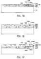
- FIG. 1A to 1 Iare schematic diagrams showing the sectional view of the structure of the first embodiment of the present invention.
- FIG. 2A to 2 Care schematic diagrams showing the sectional view of the structure of the second embodiment of the present invention.
- FIG. 2D to 2 Eare schematic diagrams showing the sectional view of the formation of inwardly protruded areas in the organic substrate of the structure of the second embodiment of the present invention.
- FIG. 3A to 3 Care schematic diagrams showing the sectional view of the structure of the third embodiment of the present invention.
- FIG. 4A to 4 Iare schematic diagrams showing the sectional view of the structure of the forth embodiment of the present invention.
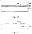
- FIG. 5A to 5 Eare schematic diagrams showing the sectional view of the structure of the fifth embodiment of the present invention.
- FIG. 6is a schematic diagram showing the section view of the chip package structure of a preferred embodiment of the present invention with one die.
- FIG. 7is a schematic diagram showing the section view of the chip package structure of a preferred embodiment of the present invention with a plurality of dies.
- FIG. 8is a magnified diagram showing the sectional view of the chip package structure of a preferred embodiment of the present invention.
- FIG. 9A, 9Bare schematic diagrams of the top and side view respectively of the patterned wiring layer of the thin-film circuit layer with a passive device.
- FIG. 10Ais a schematic diagram of the formation of a passive device by a single layer of patterned wiring layer of the thin-film circuit layer.
- FIG. 10Bis a schematic diagram of the formation of a passive device by a double layer of patterned wiring layer of the thin-film circuit layer.
- FIG. 11Ais a schematic diagram of the formation of a passive device by a single layer of patterned wiring layer of the thin-film circuit layer.
- FIG. 11Bis a schematic diagram of the formation of a passive device by a double layer of patterned wiring layer of the thin-film circuit layer.
- FIG. 11Cis a schematic diagram of the formation of a passive device by a double layer of patterned wiring layer of the thin-film circuit layer.
- an organic substrate 110 with a surface 112is provided.
- the material of the organic substratecomprises polymer resin, epoxy resin, imide resin, or the like, plastic, or thermosetting plastic.
- the fabrication of the organic substratescan be accomplished by existing printed circuit board (PCB) fabrication technique.
- the methodincludes heat pressing a plurality of insulating core boards or injection molding to form organic substrate 110 .
- a plurality of dies 120 having an active surface 122 and a corresponding backside 124is provided, where the active devices are formed on active surface 122 of dies 120 . Furthermore, dies 120 have a plurality of metal pads 126 located on active surface 122 of dies 120 acting as the output terminal of dies 120 to transmit signals to the external circuitry. Backside 124 of dies 120 is adhered to surface 112 of organic substrate 110 by a conductive paste or adhesive tape. Therefore, active surface 122 of dies 120 is facing upwards along surface 112 of organic substrate 110 .
- a filling layer 130is formed on top of surface 112 of organic substrate 110 surrounding the peripheral of dies 120 to fill the gap between dies 120 .
- the top face of filling layer 130is approximately planar to active surface 122 of dies 120 .
- the material of filling layer 130can be epoxy, polymer, or the like. After curing of filling layer 130 , a grinding or etching process is applied to planarize filling layer 130 so the top face of filling layer 130 is planar to active surface 122 of dies 120 .
- a dielectric layer 142is formed on top of filling layer 130 and active surface 122 of dies 120 .
- Dielectric layer 142is patterned according to metal pads 126 on dies 120 to form thru-holes 142 a .
- the material of dielectric layer 142can be poly-Imide (PI), benzocyclobutene (BCB), porous dielectric material, stress buffer material, or the like. Patternization of dielectric layer 142 can be performed by photo via, laser ablation, plasma etching, or the like.
- filling layer 130is used to support dielectric layer 142 so dielectric layer 142 can be formed planarized on top of organic substrate 110 and dies 120 without an uneven surface.
- dielectric layer 142also fills the peripheral of dies 120 , meaning the gap between dies 120 . Therefore the bottom structure of dielectric layer 142 can replace the structure of filling layer 130 covering entirely surface 112 of organic substrate 110 and surrounding dies 120 .
- the method of forming dielectric layer 142includes first depositing a layer of dielectric layer 142 entirely over dies 120 and organic substrate 110 , then after curing, grinding or etching process is performed to planarize dielectric layer 142 .
- a patterned wiring layer 144is formed on top of dielectric layer 142 by photolithography and sputtering, electroplating, or electro-less plating. Wherein part of the conductive material from patterned wiring layer 144 will be injected into thru-holes 142 a to form vias 142 b , copper (Cu) is used as the material for patterned wiring layer 144 .
- thru-holes 142 acan be pre-filled with a conductive material such as a conductive glue to form vias 142 b .
- patterned wiring layer 144is electrically connected to metal pads 126 of dies 120 . It is to be noted that part of patterned wiring layer 144 extends to a region outside active surface 122 of dies 120 . Dielectric layer 142 and patterned wiring layer 144 form a thin-film circuit layer 140 .
- dielectric layer 146can be formed similarly to dielectric layer 142 on top of dielectric layer 142 and patterned wiring layer 144 .
- Dielectric layer 146is also patterned to form thru-holes 146 a , whereas thru-holes 146 a correspond to bonding pads 144 a of patterned wiring layer 144 .
- a patterned wiring layer 148can be formed on dielectric layer 146 in a similar way as patterned wiring layer 144 . Wherein part of the conductive material from patterned wiring layer 148 will be injected into each thru-hole 146 a for forming a via 146 b .
- patterned wiring layer 148is electrically connected to patterned wiring layer 144 by vias 146 b , and further electrically connected to metal pads 126 of die 120 by vias 142 b of thru-hole 142 a . Therefore, thin-film circuit layer 140 further comprises dielectric layer 146 , a plurality of vias 146 b , and patterned wiring layer 148 .
- the number of patterned wiring layers ( 144 , 148 . . . ) and dielectric layers ( 142 , 146 . . . ) for electrical insulationmay be increased. All patterned wiring layers ( 144 , 148 . . . ) are electrically connected by vias ( 146 b . . . ) of thru-holes ( 146 a . . . ). However if only the first patterned wiring layer 144 is required to entirely redistribute metal pads 126 of dies 120 on organic substrate 110 , extra dielectric layers ( 146 . . .
- thin-film circuit layer 140comprises at least one dielectric layer 142 , one patterned wiring layer 144 , and a plurality of vias 142 b .
- patterned wiring layer ( 144 , 148 . . . ) and vias ( 142 b , 146 b . . . ) of thin-film circuit layer 140form an external circuitry of thin-film circuit layer 140 .
- a patterned passivation layer 150is formed on top of dielectric layer 146 and patterned wiring layer 148 .
- Patterned passivation layer 150is used to protect patterned wiring layer 148 and expose the plurality of bonding pads 148 a of patterned wiring layer 148 , whereas some of bonding pads 148 a are in a region outside active surface 122 of dies 120 .
- the redistribution of metal pads 126 on organic substrate 110requires multiple layers of patterned wiring layers ( 144 , 148 . . . ) and a patterned passivation layer 150 formed on the very top, which is furthest away from organic substrate 110 .
- patterned passivation layer 150will be formed directly on patterned wiring layer 144 .
- the material of patterned passivation layer 150can be anti-solder insulating coating or other insulating material.
- a bonding point 160can be placed on bonding pads 148 a serving as an interface for electrically connecting dies 120 to the external circuitry.
- bonding point 160 illustrated in FIG. 1His a ball but it is not limited to any formation, which might include a bump, pin, or the like.
- ball connectormaybe solder ball
- bump connectormaybe solder bump, gold bump, or the like.
- the first embodiment of the present inventionis a chip package structure with an organic substrate and a plurality of dies on the organic substrate.
- the external circuitry of the thin-film circuit layerallows the metal pads of the die to fan out.
- bonding pads corresponding to the metal pads of the diessuch as solders balls, bumps, or pins as the signal input terminals, the distance of the signal path is effectively decreased. As a result, signal delay and attenuation are reduced to increase performance of the die.
- the present inventionuses existing technology on and equipment for fabricating PCB for the fabrication of the organic substrate by heat pressing a plurality of insulating core boards.
- the organic substratecan also be fabricated in large volume by injection molding. As a result of the low fabrication and material cost of the organic substrate, the cost of chip packaging is also lowered.
- the second embodiment of the present inventiondiffers from the first embodiment by having inwardly protruded areas in the organic substrate. This area is for placement of the die with the backside of the die adhered to the bottom of the area so the overall thickness of the chip package structure is reduced.
- FIG. 2A to 2 Care schematic diagrams of the sectional view of the second embodiment illustrating the fabrication of the structure.
- an organic substrate 210 with a surface 212is provided.
- a plurality of inwardly protruded areas 214is formed on surface 212 of organic substrate 210 by machining such as milling.
- the depth of each inwardly protruded area 214is approximately equal to the thickness of die 220 , therefore the outline and depth of inwardly protruded areas 214 will be the same as dies 220 in FIG. 2C.
- backside 224 of dies 220is adhered to the bottom of inwardly protruded areas 214 so dies 220 are inlayed in inwardly protruded areas 214 .
- Active surface 222 of dies 220is exposed along surface 212 of organic substrate 210 .
- An alternative method of forming inwardly protruded areas 214 in organic substrate 210 in FIG. 2Bis applying the existing technique is fabricating PCB on two core boards: a first organic layer 210 a and a second organic layer 210 b , as illustrated in FIG. 2D.
- Organic layer 210 ahas openings 214 a and by overlapping the first organic layer 210 a and the second organic layer 210 b and heat pressing them together, openings 214 a in organic layer 210 a will form inwardly protruded areas 214 in organic layer 210 b as seen before in FIG. 2B, as illustrated in FIG. 2E.
- the thickness of organic layer 210 ais approximately equal to that of die 220 so the depth of inwardly protruded areas 214 is approximately equal to the thickness of die 220 .
- the second embodiment of the present inventionis an organic substrate with a plurality of inwardly protruded areas for inlaying dies by adhering the backside of the dies to the bottom of the inwardly protruded areas and exposing the active surface of the dies.
- a thin-film circuit layeris formed on top of the dies and the organic substrate to fan out the metal pads of the dies by using the external circuitry of the thin-film circuit layer. Due to the inlay of the dies in the organic substrate, thinning of the thickness of the chip package structure is effectively achieved and the surface of the organic substrate provides enough planarity and support for the formation of the thin-film circuit layer.
- the third embodiment of the present inventiondiffers from the second embodiment of the present invention by using an integrated organic substrate with at least one organic layer and one heat conducting layer.
- FIG. 3A to 3 Care schematic diagrams of the sectional view of the third embodiment illustrating the fabrication of the structure.
- an integrated organic substrate 310consists of an organic layer 310 a with multiple openings 314 a and a heat conducting layer 310 b , wherein the material of heat conducting layer 310 b maybe metal.
- organic layer 310 ais placed overlapping heat conducting layer 310 b so openings 314 a of organic layer 310 a form inwardly protruded areas 314 on heat conducting layer 310 b .
- backside 324 of die 320is adhered to the bottom of inwardly protruded areas 314 so dies 320 are inlayed in organic substrate 310 with active surface 322 of die 320 exposed along surface 312 of organic board 310 .
- FIG. 3Aorganic layer 310 a with openings 314 a is provided, openings 314 a are formed at the same time when organic layer 310 a is formed for example by injection molding.
- FIG. 3Borganic layer 310 a is overlapped on heat conducting layer 310 b so openings 314 a of organic layer 310 a can form inwardly protruded areas 314 on the surface of heat conducting layer 310 b.
- the third embodiment of the present inventionis an integrated organic substrate with an organic layer with a plurality of openings and a heat conducting layer.
- the openings in the organic layerwill form the inwardly protruded areas in the integrated organic substrate.
- the backside of the dieadheres to the bottom of the inwardly protruded areas so the dies are inlayed in the inwardly protruded areas and exposing the active surface of the dies.
- This integrated organic substratecan efficiently dissipate heat from the dies to the outside because the bottom of the inwardly protruded area is the surface of the heat conducting material.
- the surface of the organic substrateprovides enough planarity and support for the formation of the thin-film circuit layer.
- FIG. 4A to 4 Eare schematic diagrams of the sectional view of the fourth embodiment illustrating the fabrication of the structure.
- an organic substrate 410 with a first surface 412 and a plurality of dies 420are provided.
- the dies 420have an active surface 422 , a backside 424 , and a plurality of metal pads 426 located on active surface 422 .
- the fourth embodiment of the present inventiondiffers from the third embodiment of the present invention by placing active surface 422 of die 420 downwards facing first surface 412 of organic substrate 410 .
- a filling layer 430is formed on top of first surface 412 of organic substrate 410 after active surface 422 of die 420 is adhered to first surface 412 of organic substrate 410 .
- Filling layer 430covers entirely first surface 412 of organic substrate 410 and surrounds dies 420 .
- the material of filling layer 430maybe an oxide, epoxy, or the like.
- a planarization processsuch as grinding is performed to planarize filling layer 430 and backside 424 of dies 420 .
- the thickness of the active devices and traces (not shown) on active surface 422 of die 420is much less than that of die 420 , the thickness of die 420 should not be too small because cracks or damage to the die will occur during machine handling.
- the present inventiondirectly adheres active surface 422 of dies 420 to first surface 412 of organic substrate 410 without further machine handling.
- a grinding processis performed on backside 424 of dies 420 to reduce the thickness of dies 420 .
- dies 420are ground to a very small thickness allowing the final chip package structure to be much thinner.
- a second organic substrate 440 with a second surface 442is adhered to filling layer 430 and dies 420 creating a sandwich effect with filling layer 430 and dies 420 in between two organic substrates 410 and 440 .
- Second organic substrate 440after the adhesion of second organic substrate 440 , a grinding or the like process is performed to thin the backside of organic substrate 410 to achieve a thickness of about 2 microns to 200 microns, usually about 20 microns.
- First organic substrate 410is used to provide a planar surface for dies 420 to adhere to and to serve as an insulating layer. Therefore organic substrate 410 can be replaced by substrate made of glass or other organic material.
- first thru-holes 410 aare formed on first organic substrate 410 for exposing metal pads 426 on active surface 422 of die 420 .
- First thru-holes 410 acan be formed by machine drilling, laser, plasma etching, or similar methods.
- a first patterned wiring layer 450is formed on first organic substrate 410 .
- first vias 410 b in first thru-holes 410 aare formed by either filling first thru-holes 410 a with part of the conductive material from patterned wiring layer 450 or pre-filling first thru-holes 410 a with a conductive material before the formation of patterned wiring layer 450 .
- a part of patterned wiring layer 450will extend to a region outside active surface 422 of die 420 .
- a dielectric layer 462is formed on first organic substrate 410 and first patterned wiring layer 450 . Wherein dielectric layer 462 is patterned to form a plurality of second thru-holes 462 a , which correspond to bonding pad 450 a of patterned wiring layer 450 .
- a second patterned wiring layer 464is formed on top of dielectric layer 462 .
- second vias 462 b in thru-holes 462 acan be formed by either filling second thru-holes 462 a with part of the conductive material from patterned wiring layer or pre-filling second thru-holes 462 a with a conductive material before the formation of patterned wiring layer 464 .
- first organic substrate 410can be repeatedly formed on dies 420 and organic substrate 440 .
- first organic substrate 410first patterned wiring layer 450 , dielectric layer 462 . . . , and second patterned wiring layer 464 . . . form thin-film circuit layer 460 .
- First vias 410 b , first patterned wiring layer 450 , second vias 462 b . . . , and second patterned wiring layer 464form the external circuitry of thin-film circuit layer 460 .
- the fourth embodiment of the present inventionis an organic substrate with the active surface of the dies adhered directly to the surface of the first organic substrate.
- a filling layeris formed over the dies and the organic substrate followed by a planarization and thinning process.
- a second organic substrateis adhered to the die and the filling layer.
- a thinning process of the first organic substrateis performed and a plurality of thru-holes filled with conductive material are formed on the first organic substrate.
- a patterned wiring layeris formed on the first organic substrate allowing the external circuitry of the thin-film circuit layer to extend to a region outside the active surface of the die to help fan out the metal pads of the die.
- the advantage of this structureis increased surface stability and accuracy because the active surface of the dies are first adhered to the surface of the first organic substrate.
- the thickness of the diecan be very small for reducing the overall thickness of the chip package because no machine handling of dies is required.
- the fifth embodiment of the present inventiontakes the first half of the fabrication process from the fourth embodiment of the present invention and combines with the second half of the fabrication process from the first embodiment of the present invention.
- FIG. 5A to 5 Eare schematic diagrams of the sectional view illustrating the fabrication of the structure.
- an active surface 522 of dies 520is adhered to a first surface 512 of a first organic substrate 510 .
- a filling layer 530is formed on top of dies 520 and first organic substrate 510 covering dies 520 .
- a planarization and thinning process of dies 520 and filling layer 530is performed to planarize backside 524 of dies 520 and filling layer 530 .
- a second organic substrate 540is formed on top of dies 520 and filling layer 530 so backside 524 of dies 520 adheres to second organic substrate 540 .
- First organic substrate 510is used to supply a planarized surface (first surface 512 ), and will be removed in later stages of the fabrication process. Therefore first organic substrate 510 can be replaced by substrates of other materials such as glass, metal, silicon, or other organic material.
- the fifth embodiment of the present inventionis an organic substrate with the active surface of the dies adhered to the surface of the first organic substrate for allowing high surface stability and accuracy. As a result, it eliminates the need of machine handling of the dies to achieve a very small thickness of the die for reducing the overall thickness of the chip package.
- FIG. 6it illustrates the schematic diagram of the sectional view of the chip package structure 600 of the present invention for a single die 620 .
- Die 620is placed on organic substrate 610 , and a thin-film circuit layer 640 is formed on top of die 620 and organic substrate 610 .
- External circuitry 642 of thin-film circuit layer 640has at least has one patterned wiring layer 642 a and a plurality of vias 642 b .
- the thickness of the inner traces inside die 620is usually under 1 micron, but because the high amount of traces collocated together so RC delay is relatively high and the power/ground bus requires a large area. As a result, the area of die 620 is not enough to accommodate the power/ground bus.
- the chip package structure 600uses thin-film circuit layer 640 and external circuitry 642 with wider, thicker, and longer traces to alleviate the problem. These traces act an interface for transmitting signals for the internal circuitry of die 620 or the power/ground bus of die 620 . This will improve the performance of die 620 .
- FIG. 8it illustrates a magnified view of the sectional view of the chip package structure of the present invention.
- Active surface 622 of die 620has a plurality of active devices 628 a , 628 b , and an internal circuitry 624 .
- the internal circuitry 624forms a plurality of metal pads 626 on the surface of die 620 . Therefore signals are transmitted from active devices 628 a to external circuitry 642 via internal circuitry 624 of die 620 , and from external circuitry 642 back to another active device 628 b via internal circuitry 624 .
- the traces of external circuitry 642are wider, longer, and thicker than that of internal circuitry 624 for providing an improved transmission path.
- external circuitry 642further comprises at least one passive device 644 including a capacitor, an inductor, a resistor, a wave-guide, a filter, a micro electronic mechanical sensor (MEMS), or the like.
- Passive device 644can be located on a single layer of patterned wiring layer 642 a or between two layers of patterned wiring layers 642 a .
- passive device 644can be formed by printing or other method on two bonding points on patterned wiring layer 642 a when forming thin-film layer 640 .
- a comb-shape passive device 644(such as a comb capacitor) is formed directly on a single patterned wiring layer.
- FIG. 10Aa comb-shape passive device 644 (such as a comb capacitor) is formed directly on a single patterned wiring layer.
- passive device 644(such as a capacitor) is formed between two layers of patterned wiring layers 642 a with an insulating material 646 in between. Wherein the original dielectric layer (not shown) can replace insulating material 646 .
- passive device 644(such as an inductor) is formed by making a single layer of patterned wiring layer 642 a into a circular or square (not shown) spiral.
- column-shape passive device 644(such as an inductor) is formed by using two layers of patterned wiring layers 642 a and a plurality of vias 642 b to surround an insulating material 646 forming a column.
- FIG. 11Apassive device 644 (such as an inductor) is formed by making a single layer of patterned wiring layer 642 a into a circular or square (not shown) spiral.
- column-shape passive device 644(such as an inductor) is formed by using two layers of patterned wiring layers 642 a and a plurality of vias 642 b
- circular-shaped passive device 644(such as an inductor) is formed by using slanted traces from two layers of patterned wiring layers and a plurality of vias 642 b to surround an insulating material 646 in a circular manner forming a pie.
- the above structuresallow the original externally welded passive devices to be integrated into the inside of the chip package structure.
- FIG. 6illustrates a chip package structure 600 for a single die 620 but FIG. 7 illustrates a chip package structure 700 for a plurality of dies.
- Chip package structure 700 in FIG. 7differs from chip package structure 600 in FIG. 6 by having a die module 720 , which comprises at least one or more dies such as die 720 a , 720 b .
- Die 720 a , 720 bare electrically connected by the external circuitry of the thin-film circuit layer.
- the function of die 720 a , 720 bcan be the same or different and can be integrated together by external circuitry 742 to form a multi-die module (MCM) by packaging same or different dies into one chip package structure.
- MCMmulti-die module
- the present inventionprovides a chip packaging method by adhering a die to an organic substrate or to an inwardly protruded area of an organic substrate, and forming a thin-film circuit layer with bonding pads and points above the die and organic substrate.
- This structurecan fan out the metal pads on the die to achieve a thin chip package structure with high pin count.
- the chip package of the present inventionis performed directly on the die and the organic substrate for fanning out the metal pads on the die. It does not require flip chip or wire bonding to connect the die to the micro-spaced contact points of a package substrate or carrier.
- the present inventioncan reduce cost because the package substrate with micro-spaced contacts is very expensive.
- the signal transmission path of the present inventionis reduced to lessen the effect of signal delay and attenuation, which improves the performance of the die.
- the present inventionuses organic substrate as the package substrate of a chip carrier.
- the organic substratecan be formed by existing PCB fabrication method such as heating pressing a plurality of insulating core boards or injection molding for high volume production.
- existing PCB fabrication methodsuch as heating pressing a plurality of insulating core boards or injection molding for high volume production.
- the abundance of organic material and existing well-known-in-the-art technique on fabrication of organic materialcan greatly reduce cost of the organic substrate to lower the cost of the chip packaging.
- the third embodiment of the present inventionprovides an integrated substrate comprises an organic layer and a heat conducting layer.
- a plurality of openingscan be pre-formed on the organic layer so inwardly protruded areas are formed for inlaying the die when the organic layer overlaps the heat conducting layer.
- the heat conducting layerhelps to dissipate heat to the outside from the die during operation, which will effectively increase performance.
- the thin-film layer circuit of the present inventionis used to transmit signals between two main active devices inside the die, used as a power/ground bus, or used to add in passive devices. Furthermore, the chip package structure of the present invention can accommodate one or more dies with similar or different functions.
- the external circuitry of the thin-film circuit layerelectrically connects the multiple dies together and can be used in a MCM package.
- the chip package structure of the present inventionadapts the MCM, the external circuitry of the thin-film circuit layer, the passive devices of the external circuitry to form a package that is called “system in package”.
Landscapes
- Engineering & Computer Science (AREA)
- Computer Hardware Design (AREA)
- Power Engineering (AREA)
- Microelectronics & Electronic Packaging (AREA)
- General Physics & Mathematics (AREA)
- Physics & Mathematics (AREA)
- Condensed Matter Physics & Semiconductors (AREA)
- Manufacturing & Machinery (AREA)
- Ceramic Engineering (AREA)
- Semiconductor Integrated Circuits (AREA)
- Internal Circuitry In Semiconductor Integrated Circuit Devices (AREA)
- Structures For Mounting Electric Components On Printed Circuit Boards (AREA)
- Wire Bonding (AREA)
Abstract
Description
- This application claims the priority benefit of Taiwan application serial no. 90133093, filed Dec. 31, 2001.[0001]
- 1. Field of the Invention[0002]
- The present invention relates to an integrated chip package structure and method of manufacture the same. More particularly, the present invention relates to an integrated chip package structure and method of manufacture the same using organic substrate.[0003]
- 2. Description of Related Art[0004]
- In the recent years, the development of advanced technology is on the cutting edge. As a result, high-technology electronics manufacturing industries launch more feature-packed and humanized electronic products These new products that hit the showroom are lighter, thinner, and smaller in design. In the manufacturing of these electronic products, the key component has to be the integrated circuit (IC) chip inside any electronic product.[0005]
- The operability, performance, and life of an IC chip are greatly affected by its circuit design, wafer manufacturing, and chip packaging. For this present invention, the focus will be on chip packaging technique. Since the features and speed of IC chips are increasing rapidly, the need for increasing the conductivity of the circuitry is necessary so that the signal delay and attenuation of the dies to the external circuitry are reduced. A chip package that allows good thermal dissipation and protection of the IC chips with a small overall dimension of the package is also necessary for higher performance chips. These are the goals to be achieved in chip packaging.[0006]
- There are a vast variety of existing chip package techniques such as ball grid array (BGA), wire bonding, flip chip, etc . . . for mounting a die on a substrate via the bonding points on both the die and the substrate. The inner traces helps to fan out the bonding points on the bottom of the substrate. The solder balls are separately planted on the bonding points for acting as an interface for the die to electrically connect to the external circuitry. Similarly, pin grid array (PGA) is very much like BGA, which replaces the balls with pins on the substrate and PGA also acts an interface for the die to electrically connect to the external circuitry.[0007]
- Both BGA and PGA packages require wiring or flip chip for mounting the die on the substrate. The inner traces in the substrate fan out the bonding points on the substrate, and electrical connection to the external circuitry is carried out by the solder balls or pins on the bonding points. As a result, this method fails to reduce the distance of the signal transmission path but in fact increase the signal path distance. This will increase signal delay and attenuation and decrease the performance of the chip.[0008]
- Wafer level chip scale package (WLCSP) has an advantage of being able to print the redistribution circuit directly on the die by using the peripheral area of the die as the bonding points It is achieved by redistributing an area array on the surface of the die, which can fully utilize the entire area of the die. The bonding points are located on the redistribution circuit by forming flip chip bumps so the bottom side of the die connects directly to the printed circuit board (PCB) with micro-spaced bonding points.[0009]
- Although WLCSP can greatly reduce the signal path distance, it is still very difficult to accommodate all the bonding points on the die surface as the integration of die and internal components gets higher. The pin count on the die increases as integration gets higher so the redistribution of pins in an area array is difficult to achieve. Even if the redistribution of pins is successful, the distance between pins will be too small to meet the pitch of a printed circuit board (PCB).[0010]
- Therefore the present invention provides an integrated chip package structure and method of manufacturing the same that uses the original bonding points of the die and connect them to an external circuitry of a thin-film circuit layer to achieve redistribution. The spacing between the redistributed bonding points matches the pitch of a PCB.[0011]
- In order to achieve the above object, the present invention presents an integrated chip package structure and method of manufacturing the same by adhering the backside of a die to an organic substrate, wherein the active surface of the die has a plurality of metal pads. A thin-film circuit layer is formed on top of the die and the organic substrate, where the thin-film circuit layer has an external circuitry that is electrically connected to the metal pads of the die. The external circuitry extends to a region that is outside the active area of the dies and has a plurality of bonding pads located on the surface of the thin-film layer circuit. The active surface of the die has an internal circuitry and a plurality of active devices, where signals can be transmitted from one active device to the external circuitry via the internal circuitry, then from the external circuitry back to another active device via the internal circuitry. Furthermore, the organic substrate has at least one inwardly protruded area so the backside of the die can be adhered inside the inwardly protruded area and exposing the active surface of the die. Wherein the organic substrate is composed of an organic layer and a heat conducting material formed overlapping and the inwardly protruded areas are formed by overlapping the organic substrate with openings on the heat conducting layer. Furthermore, the present chip package structure allows multiple dies with same or different functions to be packaged into one integrated chip package and permits electrically connection between the dies by the external circuitry.[0012]
- It is to be understood that both the foregoing general description and the following detailed description are exemplary, and are intended to provide further explanation of the invention as claimed.[0013]
- The accompanying drawings are included to provide a further understanding of the invention, and are incorporated in and constitute a part of this specification. The drawings illustrate embodiments of the invention and, together with the description, serve to explain the principles of the invention. In the drawings,[0014]
- FIG. 1A to[0015]1I are schematic diagrams showing the sectional view of the structure of the first embodiment of the present invention.
- FIG. 2A to[0016]2C are schematic diagrams showing the sectional view of the structure of the second embodiment of the present invention.
- FIG. 2D to[0017]2E are schematic diagrams showing the sectional view of the formation of inwardly protruded areas in the organic substrate of the structure of the second embodiment of the present invention.
- FIG. 3A to[0018]3C are schematic diagrams showing the sectional view of the structure of the third embodiment of the present invention.
- FIG. 4A to[0019]4I are schematic diagrams showing the sectional view of the structure of the forth embodiment of the present invention.
- FIG. 5A to[0020]5E are schematic diagrams showing the sectional view of the structure of the fifth embodiment of the present invention.
- FIG. 6 is a schematic diagram showing the section view of the chip package structure of a preferred embodiment of the present invention with one die.[0021]
- FIG. 7 is a schematic diagram showing the section view of the chip package structure of a preferred embodiment of the present invention with a plurality of dies.[0022]
- FIG. 8 is a magnified diagram showing the sectional view of the chip package structure of a preferred embodiment of the present invention.[0023]
- FIG. 9A, 9B are schematic diagrams of the top and side view respectively of the patterned wiring layer of the thin-film circuit layer with a passive device.[0024]
- FIG. 10A is a schematic diagram of the formation of a passive device by a single layer of patterned wiring layer of the thin-film circuit layer.[0025]
- FIG. 10B is a schematic diagram of the formation of a passive device by a double layer of patterned wiring layer of the thin-film circuit layer.[0026]
- FIG. 11A is a schematic diagram of the formation of a passive device by a single layer of patterned wiring layer of the thin-film circuit layer.[0027]
- FIG. 11B is a schematic diagram of the formation of a passive device by a double layer of patterned wiring layer of the thin-film circuit layer.[0028]
- FIG. 11C is a schematic diagram of the formation of a passive device by a double layer of patterned wiring layer of the thin-film circuit layer.[0029]
- Please refer to FIG. 1A, an[0030]
organic substrate 110 with asurface 112 is provided. The material of the organic substrate comprises polymer resin, epoxy resin, imide resin, or the like, plastic, or thermosetting plastic. The fabrication of the organic substrates can be accomplished by existing printed circuit board (PCB) fabrication technique. The method includes heat pressing a plurality of insulating core boards or injection molding to formorganic substrate 110. - A plurality of dies[0031]120 having an
active surface 122 and acorresponding backside 124 is provided, where the active devices are formed onactive surface 122 of dies120. Furthermore, dies120 have a plurality ofmetal pads 126 located onactive surface 122 of dies120 acting as the output terminal of dies120 to transmit signals to the external circuitry.Backside 124 of dies120 is adhered to surface112 oforganic substrate 110 by a conductive paste or adhesive tape. Therefore,active surface 122 of dies120 is facing upwards alongsurface 112 oforganic substrate 110. - Please refer to FIG. 1B, when adhering die[0032]120 to
organic substrate 110, afilling layer 130 is formed on top ofsurface 112 oforganic substrate 110 surrounding the peripheral of dies120 to fill the gap between dies120. Wherein the top face of fillinglayer 130 is approximately planar toactive surface 122 of dies120. The material of fillinglayer 130 can be epoxy, polymer, or the like. After curing of fillinglayer 130, a grinding or etching process is applied to planarize fillinglayer 130 so the top face of fillinglayer 130 is planar toactive surface 122 of dies120. - Please refer to FIG. 1C, after the formation of filling[0033]
layer 130 onorganic substrate 110, adielectric layer 142 is formed on top of fillinglayer 130 andactive surface 122 of dies120.Dielectric layer 142 is patterned according tometal pads 126 on dies120 to form thru-holes 142a. The material ofdielectric layer 142 can be poly-Imide (PI), benzocyclobutene (BCB), porous dielectric material, stress buffer material, or the like. Patternization ofdielectric layer 142 can be performed by photo via, laser ablation, plasma etching, or the like. - Please continue to refer to FIG. 1C, filling[0034]
layer 130 is used to supportdielectric layer 142 sodielectric layer 142 can be formed planarized on top oforganic substrate 110 and dies120 without an uneven surface. As a result, afterdielectric layer 142 is formed onsurface 112 oforganic substrate 110 andactive surface 122 of dies120,dielectric layer 142 also fills the peripheral of dies120, meaning the gap between dies120. Therefore the bottom structure ofdielectric layer 142 can replace the structure of fillinglayer 130 covering entirely surface112 oforganic substrate 110 and surrounding dies120. The method of formingdielectric layer 142 includes first depositing a layer ofdielectric layer 142 entirely over dies120 andorganic substrate 110, then after curing, grinding or etching process is performed to planarizedielectric layer 142. - Please refer to FIG. 1D, after forming[0035]
dielectric layer 142 and patterningdielectric layer 142 to form thru-holes 142a, a patternedwiring layer 144 is formed on top ofdielectric layer 142 by photolithography and sputtering, electroplating, or electro-less plating. Wherein part of the conductive material from patternedwiring layer 144 will be injected into thru-holes 142ato form vias142b, copper (Cu) is used as the material for patternedwiring layer 144. Moreover, thru-holes 142acan be pre-filled with a conductive material such as a conductive glue to form vias142b. Therefore no matter if the thru-holes are filled with the conductive material from patternedwiring layer 144 or pre-filled with a conductive material, patternedwiring layer 144 is electrically connected tometal pads 126 of dies120. It is to be noted that part of patternedwiring layer 144 extends to a region outsideactive surface 122 of dies120.Dielectric layer 142 and patternedwiring layer 144 form a thin-film circuit layer 140. - Please refer to FIG. 1E, after the formation of patterned[0036]
wiring layer 144, anotherdielectric layer 146 can be formed similarly todielectric layer 142 on top ofdielectric layer 142 and patternedwiring layer 144.Dielectric layer 146 is also patterned to form thru-holes 146a, whereas thru-holes 146acorrespond tobonding pads 144aof patternedwiring layer 144. - Please refer to FIG. 1F, after the formation and patternization of[0037]
dielectric layer 146 to form thru-holes 146a, a patternedwiring layer 148 can be formed ondielectric layer 146 in a similar way as patternedwiring layer 144. Wherein part of the conductive material from patternedwiring layer 148 will be injected into each thru-hole 146afor forming a via146b. By the same token, patternedwiring layer 148 is electrically connected to patternedwiring layer 144 byvias 146b, and further electrically connected tometal pads 126 ofdie 120 byvias 142bof thru-hole 142a. Therefore, thin-film circuit layer 140 further comprisesdielectric layer 146, a plurality ofvias 146b, and patternedwiring layer 148. - Please continue to refer to FIG. 1F, in order to redistribute all[0038]
metal pads 126 of dies120 onorganic substrate 110, the number of patterned wiring layers (144,148 . . . ) and dielectric layers (142,146 . . . ) for electrical insulation may be increased. All patterned wiring layers (144,148 . . . ) are electrically connected by vias (146b. . . ) of thru-holes (146a. . . ). However if only the firstpatterned wiring layer 144 is required to entirely redistributemetal pads 126 of dies120 onorganic substrate 110, extra dielectric layers (146 . . . ) and patterned wiring layers (148 . . . ) will no longer be required in the structure. In other words, thin-film circuit layer 140 comprises at least onedielectric layer 142, one patternedwiring layer 144, and a plurality ofvias 142b. Wherein patterned wiring layer (144,148 . . . ) and vias (142b,146b. . . ) of thin-film circuit layer 140 form an external circuitry of thin-film circuit layer 140. - Please refer to FIG. 1G, after the formation of patterned[0039]
wiring layer 148, a patternedpassivation layer 150 is formed on top ofdielectric layer 146 and patternedwiring layer 148. Patternedpassivation layer 150 is used to protect patternedwiring layer 148 and expose the plurality ofbonding pads 148aof patternedwiring layer 148, whereas some ofbonding pads 148aare in a region outsideactive surface 122 of dies120. As previously mentioned, the redistribution ofmetal pads 126 onorganic substrate 110 requires multiple layers of patterned wiring layers (144,148 . . . ) and a patternedpassivation layer 150 formed on the very top, which is furthest away fromorganic substrate 110. However, if only patternedwiring layer 144 is required to redistribute allmetal pads 126 of dies120 onorganic substrate 110, patternedpassivation layer 150 will be formed directly on patternedwiring layer 144. The material of patternedpassivation layer 150 can be anti-solder insulating coating or other insulating material. - Please refer to FIG. 1H, after the formation of patterned[0040]
passivation layer 150, abonding point 160 can be placed onbonding pads 148aserving as an interface for electrically connecting dies120 to the external circuitry. Whereinbonding point 160 illustrated in FIG. 1H is a ball but it is not limited to any formation, which might include a bump, pin, or the like. Wherein ball connector maybe solder ball, and bump connector maybe solder bump, gold bump, or the like. - Please refer to FIG. 1I, after the formation of bonding points[0041]160 on
bonding pads 148a, a singularization process of packaged die120 by mechanical or laser cutting is performed along the dotted line as indicated in the diagram. Afterwards, the chip package structure of the die is completed. - According to the above, the first embodiment of the present invention is a chip package structure with an organic substrate and a plurality of dies on the organic substrate. The external circuitry of the thin-film circuit layer allows the metal pads of the die to fan out. By forming bonding pads corresponding to the metal pads of the dies such as solders balls, bumps, or pins as the signal input terminals, the distance of the signal path is effectively decreased. As a result, signal delay and attenuation are reduced to increase performance of the die.[0042]
- The present invention uses existing technology on and equipment for fabricating PCB for the fabrication of the organic substrate by heat pressing a plurality of insulating core boards. Alternatively, the organic substrate can also be fabricated in large volume by injection molding. As a result of the low fabrication and material cost of the organic substrate, the cost of chip packaging is also lowered.[0043]
- The second embodiment of the present invention differs from the first embodiment by having inwardly protruded areas in the organic substrate. This area is for placement of the die with the backside of the die adhered to the bottom of the area so the overall thickness of the chip package structure is reduced. FIG. 2A to[0044]2C are schematic diagrams of the sectional view of the second embodiment illustrating the fabrication of the structure.
- Please refer to FIG. 2A, an[0045]
organic substrate 210 with asurface 212 is provided. In FIG. 2B, a plurality of inwardly protrudedareas 214 is formed onsurface 212 oforganic substrate 210 by machining such as milling. The depth of each inwardly protrudedarea 214 is approximately equal to the thickness ofdie 220, therefore the outline and depth of inwardly protrudedareas 214 will be the same as dies220 in FIG. 2C. In FIG. 2C,backside 224 of dies220 is adhered to the bottom of inwardly protrudedareas 214 so dies220 are inlayed in inwardly protrudedareas 214.Active surface 222 of dies220 is exposed alongsurface 212 oforganic substrate 210. - An alternative method of forming inwardly protruded[0046]
areas 214 inorganic substrate 210 in FIG. 2B is applying the existing technique is fabricating PCB on two core boards: a firstorganic layer 210aand a secondorganic layer 210b, as illustrated in FIG. 2D.Organic layer 210ahasopenings 214aand by overlapping the firstorganic layer 210aand the secondorganic layer 210band heat pressing them together,openings 214ainorganic layer 210awill form inwardly protrudedareas 214 inorganic layer 210bas seen before in FIG. 2B, as illustrated in FIG. 2E. The thickness oforganic layer 210ais approximately equal to that ofdie 220 so the depth of inwardly protrudedareas 214 is approximately equal to the thickness ofdie 220. - The structure of the second embodiment of the present invention after FIG. 2C will follow FIG. 1C to[0047]1I from the first embodiment of the present invention, therefore it will not be repeated.
- The second embodiment of the present invention is an organic substrate with a plurality of inwardly protruded areas for inlaying dies by adhering the backside of the dies to the bottom of the inwardly protruded areas and exposing the active surface of the dies. A thin-film circuit layer is formed on top of the dies and the organic substrate to fan out the metal pads of the dies by using the external circuitry of the thin-film circuit layer. Due to the inlay of the dies in the organic substrate, thinning of the thickness of the chip package structure is effectively achieved and the surface of the organic substrate provides enough planarity and support for the formation of the thin-film circuit layer.[0048]
- The third embodiment of the present invention differs from the second embodiment of the present invention by using an integrated organic substrate with at least one organic layer and one heat conducting layer. FIG. 3A to[0049]3C are schematic diagrams of the sectional view of the third embodiment illustrating the fabrication of the structure.
- Please refer to FIG. 3A, an integrated organic substrate[0050]310 consists of an
organic layer 310awithmultiple openings 314aand aheat conducting layer 310b, wherein the material ofheat conducting layer 310bmaybe metal. In FIG. 3B,organic layer 310ais placed overlappingheat conducting layer 310bsoopenings 314aoforganic layer 310aform inwardly protrudedareas 314 onheat conducting layer 310b. Following in FIG. 3C,backside 324 ofdie 320 is adhered to the bottom of inwardly protrudedareas 314 so dies320 are inlayed in organic substrate310 withactive surface 322 ofdie 320 exposed alongsurface 312 of organic board310. - The following presents two ways of forming integrated organic substrate[0051]310 with inwardly protruded
areas 314 as shown in FIG. 3B. In FIG. 3A,organic layer 310awithopenings 314ais provided,openings 314aare formed at the same time whenorganic layer 310ais formed for example by injection molding. In FIG. 3B,organic layer 310ais overlapped onheat conducting layer 310bsoopenings 314aoforganic layer 310acan form inwardly protrudedareas 314 on the surface ofheat conducting layer 310b. - The structure of the third embodiment of the present invention after FIG. 3C will follow FIG. 1C to[0052]1I from the first embodiment of the present invention, therefore it will not be repeated.
- The third embodiment of the present invention is an integrated organic substrate with an organic layer with a plurality of openings and a heat conducting layer. The openings in the organic layer will form the inwardly protruded areas in the integrated organic substrate. The backside of the die adheres to the bottom of the inwardly protruded areas so the dies are inlayed in the inwardly protruded areas and exposing the active surface of the dies. This integrated organic substrate can efficiently dissipate heat from the dies to the outside because the bottom of the inwardly protruded area is the surface of the heat conducting material. The surface of the organic substrate provides enough planarity and support for the formation of the thin-film circuit layer.[0053]
- The fourth embodiment of the present invention is slightly different from the first three embodiments. FIG. 4A to[0054]4E are schematic diagrams of the sectional view of the fourth embodiment illustrating the fabrication of the structure.
- Please refer to FIG. 4A, an[0055]
organic substrate 410 with afirst surface 412 and a plurality of dies420 are provided. The dies420 have anactive surface 422, abackside 424, and a plurality ofmetal pads 426 located onactive surface 422. The fourth embodiment of the present invention differs from the third embodiment of the present invention by placingactive surface 422 ofdie 420 downwards facingfirst surface 412 oforganic substrate 410. - Please refer to FIG. 4B, a[0056]
filling layer 430 is formed on top offirst surface 412 oforganic substrate 410 afteractive surface 422 ofdie 420 is adhered tofirst surface 412 oforganic substrate 410. Fillinglayer 430 covers entirelyfirst surface 412 oforganic substrate 410 and surrounds dies420. The material of fillinglayer 430 maybe an oxide, epoxy, or the like. - Please refer to FIG. 4C, after the formation of filling[0057]
layer 430, a planarization process such as grinding is performed to planarize fillinglayer 430 andbackside 424 of dies420. Although the thickness of the active devices and traces (not shown) onactive surface 422 ofdie 420 is much less than that ofdie 420, the thickness ofdie 420 should not be too small because cracks or damage to the die will occur during machine handling. However the present invention directly adheresactive surface 422 of dies420 tofirst surface 412 oforganic substrate 410 without further machine handling. Afterwards a grinding process is performed onbackside 424 of dies420 to reduce the thickness of dies420. As a result, dies420 are ground to a very small thickness allowing the final chip package structure to be much thinner. - Please refer to FIG. 4D, after the planarization of filling[0058]
layer 430 and dies420, a secondorganic substrate 440 with asecond surface 442 is adhered to fillinglayer 430 and dies420 creating a sandwich effect with fillinglayer 430 and dies420 in between twoorganic substrates - Please refer to FIG. 4E, after the adhesion of second[0059]
organic substrate 440, a grinding or the like process is performed to thin the backside oforganic substrate 410 to achieve a thickness of about 2 microns to 200 microns, usually about 20 microns. Firstorganic substrate 410 is used to provide a planar surface for dies420 to adhere to and to serve as an insulating layer. Thereforeorganic substrate 410 can be replaced by substrate made of glass or other organic material. - Please refer to FIG. 4F, after the thinning of first[0060]
organic substrate 410, a plurality of first thru-holes 410aare formed on firstorganic substrate 410 for exposingmetal pads 426 onactive surface 422 ofdie 420. First thru-holes 410acan be formed by machine drilling, laser, plasma etching, or similar methods. - Please refer to FIG. 4G, a first[0061]
patterned wiring layer 450 is formed on firstorganic substrate 410. Using the same method disclosed in the first embodiment of the present invention,first vias 410bin first thru-holes 410aare formed by either filling first thru-holes 410awith part of the conductive material from patternedwiring layer 450 or pre-filling first thru-holes 410awith a conductive material before the formation of patternedwiring layer 450. A part of patternedwiring layer 450 will extend to a region outsideactive surface 422 ofdie 420. - Please refer to FIG. 4H, a[0062]
dielectric layer 462 is formed on firstorganic substrate 410 and firstpatterned wiring layer 450. Whereindielectric layer 462 is patterned to form a plurality of second thru-holes 462a, which correspond tobonding pad 450aof patternedwiring layer 450. - Please refer to FIG. 4I, a second[0063]
patterned wiring layer 464 is formed on top ofdielectric layer 462. Using the same method as above,second vias 462bin thru-holes 462acan be formed by either filling second thru-holes 462awith part of the conductive material from patterned wiring layer or pre-filling second thru-holes 462awith a conductive material before the formation of patternedwiring layer 464. Similarly, in order to redistributemetal pads 426 of dies420 on secondorganic substrate 440, dielectric layer (462), second vias (462a. . . ), and second patterned wiring layer (464 . . . ) can be repeatedly formed on dies420 andorganic substrate 440. Wherein firstorganic substrate 410, firstpatterned wiring layer 450,dielectric layer 462 . . . , and secondpatterned wiring layer 464 . . . form thin-film circuit layer 460.First vias 410b, firstpatterned wiring layer 450,second vias 462b. . . , and secondpatterned wiring layer 464 form the external circuitry of thin-film circuit layer 460. - The structure of the fourth embodiment of the present invention after FIG. 4I will follow FIG. 1G to[0064]1I from the first embodiment of the present invention, therefore it will not be repeated.
- The fourth embodiment of the present invention is an organic substrate with the active surface of the dies adhered directly to the surface of the first organic substrate. A filling layer is formed over the dies and the organic substrate followed by a planarization and thinning process. Afterwards, a second organic substrate is adhered to the die and the filling layer. A thinning process of the first organic substrate is performed and a plurality of thru-holes filled with conductive material are formed on the first organic substrate. Finally a patterned wiring layer is formed on the first organic substrate allowing the external circuitry of the thin-film circuit layer to extend to a region outside the active surface of the die to help fan out the metal pads of the die.[0065]
- The advantage of this structure is increased surface stability and accuracy because the active surface of the dies are first adhered to the surface of the first organic substrate. The thickness of the die can be very small for reducing the overall thickness of the chip package because no machine handling of dies is required.[0066]
- The fifth embodiment of the present invention takes the first half of the fabrication process from the fourth embodiment of the present invention and combines with the second half of the fabrication process from the first embodiment of the present invention. FIG. 5A to[0067]5E are schematic diagrams of the sectional view illustrating the fabrication of the structure.
- Please refer to FIG. 5A, an[0068]
active surface 522 of dies520 is adhered to afirst surface 512 of a firstorganic substrate 510. In FIG. 5B, afilling layer 530 is formed on top of dies520 and firstorganic substrate 510 covering dies520. In FIG. 5C, a planarization and thinning process of dies520 and fillinglayer 530 is performed toplanarize backside 524 of dies520 and fillinglayer 530. In FIG. 5D, a secondorganic substrate 540 is formed on top of dies520 and fillinglayer 530 sobackside 524 of dies520 adheres to secondorganic substrate 540. By removingfilling layer 530 and firstorganic substrate 510, the metal pads onactive surface 522 of dies520 are exposed. Firstorganic substrate 510 is used to supply a planarized surface (first surface512), and will be removed in later stages of the fabrication process. Therefore firstorganic substrate 510 can be replaced by substrates of other materials such as glass, metal, silicon, or other organic material. - The structure of the fifth embodiment of the present invention after FIG. 5E will follow FIG. 1B to[0069]1I of the first embodiment of the present invention, therefore it will not be repeated.
- The fifth embodiment of the present invention is an organic substrate with the active surface of the dies adhered to the surface of the first organic substrate for allowing high surface stability and accuracy. As a result, it eliminates the need of machine handling of the dies to achieve a very small thickness of the die for reducing the overall thickness of the chip package.[0070]
- Furthermore, please refer to FIG. 6, it illustrates the schematic diagram of the sectional view of the[0071]
chip package structure 600 of the present invention for asingle die 620.Die 620 is placed onorganic substrate 610, and a thin-film circuit layer 640 is formed on top ofdie 620 andorganic substrate 610.External circuitry 642 of thin-film circuit layer 640 has at least has one patternedwiring layer 642aand a plurality ofvias 642b. The thickness of the inner traces inside die620 is usually under 1 micron, but because the high amount of traces collocated together so RC delay is relatively high and the power/ground bus requires a large area. As a result, the area ofdie 620 is not enough to accommodate the power/ground bus. Therefore thechip package structure 600 uses thin-film circuit layer 640 andexternal circuitry 642 with wider, thicker, and longer traces to alleviate the problem. These traces act an interface for transmitting signals for the internal circuitry ofdie 620 or the power/ground bus ofdie 620. This will improve the performance ofdie 620. - Please refer to FIG. 8, it illustrates a magnified view of the sectional view of the chip package structure of the present invention.[0072]
Active surface 622 ofdie 620 has a plurality ofactive devices internal circuitry 624. Theinternal circuitry 624 forms a plurality ofmetal pads 626 on the surface ofdie 620. Therefore signals are transmitted fromactive devices 628atoexternal circuitry 642 viainternal circuitry 624 ofdie 620, and fromexternal circuitry 642 back to anotheractive device 628bviainternal circuitry 624. The traces ofexternal circuitry 642 are wider, longer, and thicker than that ofinternal circuitry 624 for providing an improved transmission path. - Please continue to refer to FIG. 6,[0073]
external circuitry 642 further comprises at least onepassive device 644 including a capacitor, an inductor, a resistor, a wave-guide, a filter, a micro electronic mechanical sensor (MEMS), or the like.Passive device 644 can be located on a single layer of patternedwiring layer 642aor between two layers of patterned wiring layers642a. In FIG. 9A, 9B,passive device 644 can be formed by printing or other method on two bonding points on patternedwiring layer 642awhen forming thin-film layer 640. In FIG. 10A, a comb-shape passive device644 (such as a comb capacitor) is formed directly on a single patterned wiring layer. In FIG. 10B, passive device644 (such as a capacitor) is formed between two layers of patterned wiring layers642awith an insulatingmaterial 646 in between. Wherein the original dielectric layer (not shown) can replace insulatingmaterial 646. In FIG. 11A, passive device644 (such as an inductor) is formed by making a single layer of patternedwiring layer 642ainto a circular or square (not shown) spiral. In FIG. 11B, column-shape passive device644 (such as an inductor) is formed by using two layers of patterned wiring layers642aand a plurality ofvias 642bto surround an insulatingmaterial 646 forming a column. In FIG. 11C, circular-shaped passive device644 (such as an inductor) is formed by using slanted traces from two layers of patterned wiring layers and a plurality ofvias 642bto surround an insulatingmaterial 646 in a circular manner forming a pie. The above structures allow the original externally welded passive devices to be integrated into the inside of the chip package structure. - FIG. 6 illustrates a[0074]
chip package structure 600 for asingle die 620 but FIG. 7 illustrates achip package structure 700 for a plurality of dies.Chip package structure 700 in FIG. 7 differs fromchip package structure 600 in FIG. 6 by having adie module 720, which comprises at least one or more dies such as die720a,720b.Die external circuitry 742 to form a multi-die module (MCM) by packaging same or different dies into one chip package structure. When multiple dies are packaged into the same chip package structure, singulation process is performed on the determined number of dies. - Following the above, the present invention provides a chip packaging method by adhering a die to an organic substrate or to an inwardly protruded area of an organic substrate, and forming a thin-film circuit layer with bonding pads and points above the die and organic substrate. This structure can fan out the metal pads on the die to achieve a thin chip package structure with high pin count.[0075]
- Comparing to the BGA or PGA package technique used in the prior art, the chip package of the present invention is performed directly on the die and the organic substrate for fanning out the metal pads on the die. It does not require flip chip or wire bonding to connect the die to the micro-spaced contact points of a package substrate or carrier. The present invention can reduce cost because the package substrate with micro-spaced contacts is very expensive. Moreover the signal transmission path of the present invention is reduced to lessen the effect of signal delay and attenuation, which improves the performance of the die.[0076]
- Furthermore, the present invention uses organic substrate as the package substrate of a chip carrier. The organic substrate can be formed by existing PCB fabrication method such as heating pressing a plurality of insulating core boards or injection molding for high volume production. The abundance of organic material and existing well-known-in-the-art technique on fabrication of organic material can greatly reduce cost of the organic substrate to lower the cost of the chip packaging.[0077]
- Furthermore, the third embodiment of the present invention provides an integrated substrate comprises an organic layer and a heat conducting layer. A plurality of openings can be pre-formed on the organic layer so inwardly protruded areas are formed for inlaying the die when the organic layer overlaps the heat conducting layer. The heat conducting layer helps to dissipate heat to the outside from the die during operation, which will effectively increase performance.[0078]
- The thin-film layer circuit of the present invention is used to transmit signals between two main active devices inside the die, used as a power/ground bus, or used to add in passive devices. Furthermore, the chip package structure of the present invention can accommodate one or more dies with similar or different functions. The external circuitry of the thin-film circuit layer electrically connects the multiple dies together and can be used in a MCM package. The chip package structure of the present invention adapts the MCM, the external circuitry of the thin-film circuit layer, the passive devices of the external circuitry to form a package that is called “system in package”.[0079]
- It will be apparent to those skilled in the art that various modifications and variations can be made to the structure of the present invention without departing from the scope or spirit of the invention. In view of the foregoing, it is intended that the present invention cover modifications and variations of this invention provided they fall within the scope of the following claims and their equivalents.[0080]
Claims (203)
Priority Applications (1)
| Application Number | Priority Date | Filing Date | Title |
|---|---|---|---|
| US10/728,150US7345365B2 (en) | 2001-12-31 | 2003-12-03 | Electronic component with die and passive device |
Applications Claiming Priority (4)
| Application Number | Priority Date | Filing Date | Title |
|---|---|---|---|
| TW090133093ATW544882B (en) | 2001-12-31 | 2001-12-31 | Chip package structure and process thereof |
| TW90133093 | 2001-12-31 | ||
| US10/055,499US7413929B2 (en) | 2001-12-31 | 2002-01-22 | Integrated chip package structure using organic substrate and method of manufacturing the same |
| US10/728,150US7345365B2 (en) | 2001-12-31 | 2003-12-03 | Electronic component with die and passive device |
Related Parent Applications (1)
| Application Number | Title | Priority Date | Filing Date |
|---|---|---|---|
| US10/055,499DivisionUS7413929B2 (en) | 2001-12-31 | 2002-01-22 | Integrated chip package structure using organic substrate and method of manufacturing the same |
Publications (2)
| Publication Number | Publication Date |
|---|---|
| US20040119097A1true US20040119097A1 (en) | 2004-06-24 |
| US7345365B2 US7345365B2 (en) | 2008-03-18 |
Family
ID=21680114
Family Applications (5)
| Application Number | Title | Priority Date | Filing Date |
|---|---|---|---|
| US10/055,499Expired - LifetimeUS7413929B2 (en) | 2001-12-31 | 2002-01-22 | Integrated chip package structure using organic substrate and method of manufacturing the same |
| US10/728,150Expired - LifetimeUS7345365B2 (en) | 2001-12-31 | 2003-12-03 | Electronic component with die and passive device |
| US10/794,472Expired - LifetimeUS7297614B2 (en) | 2001-12-31 | 2004-03-05 | Method for fabricating circuitry component |
| US12/172,275Expired - Fee RelatedUS7898058B2 (en) | 2001-12-31 | 2008-07-14 | Integrated chip package structure using organic substrate and method of manufacturing the same |
| US13/031,163Expired - Fee RelatedUS8471361B2 (en) | 2001-12-31 | 2011-02-18 | Integrated chip package structure using organic substrate and method of manufacturing the same |
Family Applications Before (1)
| Application Number | Title | Priority Date | Filing Date |
|---|---|---|---|
| US10/055,499Expired - LifetimeUS7413929B2 (en) | 2001-12-31 | 2002-01-22 | Integrated chip package structure using organic substrate and method of manufacturing the same |
Family Applications After (3)
| Application Number | Title | Priority Date | Filing Date |
|---|---|---|---|
| US10/794,472Expired - LifetimeUS7297614B2 (en) | 2001-12-31 | 2004-03-05 | Method for fabricating circuitry component |
| US12/172,275Expired - Fee RelatedUS7898058B2 (en) | 2001-12-31 | 2008-07-14 | Integrated chip package structure using organic substrate and method of manufacturing the same |
| US13/031,163Expired - Fee RelatedUS8471361B2 (en) | 2001-12-31 | 2011-02-18 | Integrated chip package structure using organic substrate and method of manufacturing the same |
Country Status (2)
| Country | Link |
|---|---|
| US (5) | US7413929B2 (en) |
| TW (1) | TW544882B (en) |
Cited By (7)
| Publication number | Priority date | Publication date | Assignee | Title |
|---|---|---|---|---|
| US20080122074A1 (en)* | 2006-11-28 | 2008-05-29 | Silicon Storage Tech., Inc. | Multi-chip electronic circuit module and a method of manufacturing |
| US7397117B2 (en) | 2002-01-19 | 2008-07-08 | Megica Corporation | Chip package with die and substrate |
| US20080163485A1 (en)* | 2007-01-10 | 2008-07-10 | Advanced Semiconductor Engineering Inc. | Manufacturing method for integrating passive component within substrate |
| US20090085187A1 (en)* | 2007-09-28 | 2009-04-02 | Ward Scott | Loading mechanism for bare die packages and lga socket |
| US20110080245A1 (en)* | 2009-09-24 | 2011-04-07 | Tsuneo Suzuki | Multilayer circuit board |
| US20120252169A1 (en)* | 2007-07-31 | 2012-10-04 | Freescale Semiconductor, Inc. | Redistributed chip packaging with thermal contact to device backside |
| WO2025155495A1 (en)* | 2024-01-15 | 2025-07-24 | Texas Instruments Incorporated | Integrated circuit with a protective layer |
Families Citing this family (95)
| Publication number | Priority date | Publication date | Assignee | Title |
|---|---|---|---|---|
| US7271489B2 (en)* | 2003-10-15 | 2007-09-18 | Megica Corporation | Post passivation interconnection schemes on top of the IC chips |
| TW517361B (en) | 2001-12-31 | 2003-01-11 | Megic Corp | Chip package structure and its manufacture process |
| TW503496B (en) | 2001-12-31 | 2002-09-21 | Megic Corp | Chip packaging structure and manufacturing process of the same |
| TW584950B (en) | 2001-12-31 | 2004-04-21 | Megic Corp | Chip packaging structure and process thereof |
| TW544882B (en) | 2001-12-31 | 2003-08-01 | Megic Corp | Chip package structure and process thereof |
| US7037805B2 (en)* | 2003-05-07 | 2006-05-02 | Honeywell International Inc. | Methods and apparatus for attaching a die to a substrate |
| US6927098B2 (en)* | 2003-05-07 | 2005-08-09 | Honeywell International Inc. | Methods and apparatus for attaching MEMS devices to housing |
| DE10355925B4 (en)* | 2003-11-29 | 2006-07-06 | Semikron Elektronik Gmbh & Co. Kg | Power semiconductor module and method of its manufacture |
| US7459781B2 (en)* | 2003-12-03 | 2008-12-02 | Wen-Kun Yang | Fan out type wafer level package structure and method of the same |
| US7514767B2 (en)* | 2003-12-03 | 2009-04-07 | Advanced Chip Engineering Technology Inc. | Fan out type wafer level package structure and method of the same |
| US7215018B2 (en) | 2004-04-13 | 2007-05-08 | Vertical Circuits, Inc. | Stacked die BGA or LGA component assembly |
| US7262121B2 (en)* | 2004-07-29 | 2007-08-28 | Micron Technology, Inc. | Integrated circuit and methods of redistributing bondpad locations |
| JP4880218B2 (en)* | 2004-12-22 | 2012-02-22 | 三洋電機株式会社 | Circuit equipment |
| EP1762928A1 (en)* | 2005-09-09 | 2007-03-14 | Agilent Technologies, Inc. | Graphics device comprising remote transfer controller for remote visualization |
| US20070114643A1 (en)* | 2005-11-22 | 2007-05-24 | Honeywell International Inc. | Mems flip-chip packaging |
| US7491567B2 (en)* | 2005-11-22 | 2009-02-17 | Honeywell International Inc. | MEMS device packaging methods |
| TW200727370A (en)* | 2006-01-12 | 2007-07-16 | Touch Micro System Tech | Integrated die packaging structure and manufacturing process thereof |
| CN100392852C (en)* | 2006-04-12 | 2008-06-04 | 江苏长电科技股份有限公司 | Flat bump type ultra-thin packaging substrate for electronic components and manufacturing method thereof |
| CN100392851C (en)* | 2006-04-12 | 2008-06-04 | 江苏长电科技股份有限公司 | Planar bump type ultra-thin packaging substrate for semiconductor components and manufacturing method thereof |
| DE102006019244B4 (en)* | 2006-04-21 | 2008-07-03 | Infineon Technologies Ag | Benefit and semiconductor device made of a composite board with semiconductor chips and plastic housing composition and method for producing the same |
| US7830004B2 (en)* | 2006-10-27 | 2010-11-09 | Taiwan Semiconductor Manufacturing Company, Ltd. | Packaging with base layers comprising alloy 42 |
| US7791199B2 (en) | 2006-11-22 | 2010-09-07 | Tessera, Inc. | Packaged semiconductor chips |
| US8569876B2 (en) | 2006-11-22 | 2013-10-29 | Tessera, Inc. | Packaged semiconductor chips with array |
| US7608538B2 (en)* | 2007-01-05 | 2009-10-27 | International Business Machines Corporation | Formation of vertical devices by electroplating |
| US8405196B2 (en) | 2007-03-05 | 2013-03-26 | DigitalOptics Corporation Europe Limited | Chips having rear contacts connected by through vias to front contacts |
| US7964961B2 (en)* | 2007-04-12 | 2011-06-21 | Megica Corporation | Chip package |
| US7687318B2 (en) | 2007-05-04 | 2010-03-30 | Stats Chippac, Ltd. | Extended redistribution layers bumped wafer |
| US8723332B2 (en)* | 2007-06-11 | 2014-05-13 | Invensas Corporation | Electrically interconnected stacked die assemblies |
| WO2008157722A1 (en)* | 2007-06-19 | 2008-12-24 | Vertical Circuits, Inc. | Wafer level surface passivation of stackable integrated circuit chips |
| TW200917391A (en)* | 2007-06-20 | 2009-04-16 | Vertical Circuits Inc | Three-dimensional circuitry formed on integrated circuit device using two-dimensional fabrication |
| US7868445B2 (en)* | 2007-06-25 | 2011-01-11 | Epic Technologies, Inc. | Integrated structures and methods of fabrication thereof with fan-out metallization on a chips-first chip layer |
| US7605092B2 (en) | 2007-06-29 | 2009-10-20 | Silicon Storage Technology, Inc. | Passive elements, articles, packages, semiconductor composites, and methods of manufacturing same |
| KR20090007120A (en)* | 2007-07-13 | 2009-01-16 | 삼성전자주식회사 | Wafer level laminated package to achieve redistribution through encapsulation and manufacturing method |
| WO2009017835A2 (en)* | 2007-07-31 | 2009-02-05 | Tessera, Inc. | Semiconductor packaging process using through silicon vias |
| WO2009020467A1 (en)* | 2007-08-07 | 2009-02-12 | Skyworks Solutions, Inc. | Near chip scale package integration process |
| US7595226B2 (en)* | 2007-08-29 | 2009-09-29 | Freescale Semiconductor, Inc. | Method of packaging an integrated circuit die |
| WO2009035849A2 (en) | 2007-09-10 | 2009-03-19 | Vertical Circuits, Inc. | Semiconductor die mount by conformal die coating |
| WO2009052150A1 (en)* | 2007-10-18 | 2009-04-23 | Vertical Circuits, Inc. | Chip scale stacked die package |
| KR101375660B1 (en)* | 2008-02-22 | 2014-03-19 | 삼성전자주식회사 | A resonator, bandpass filter and manufacturing method of resonator using overlay electromagnetic bandgap structure |
| US20090212381A1 (en)* | 2008-02-26 | 2009-08-27 | Tessera, Inc. | Wafer level packages for rear-face illuminated solid state image sensors |
| US20100053407A1 (en)* | 2008-02-26 | 2010-03-04 | Tessera, Inc. | Wafer level compliant packages for rear-face illuminated solid state image sensors |
| CN101999167B (en)* | 2008-03-12 | 2013-07-17 | 伊文萨思公司 | Support mounted electrically interconnected die assembly |
| US7863159B2 (en)* | 2008-06-19 | 2011-01-04 | Vertical Circuits, Inc. | Semiconductor die separation method |
| US9153517B2 (en) | 2008-05-20 | 2015-10-06 | Invensas Corporation | Electrical connector between die pad and z-interconnect for stacked die assemblies |
| WO2009145727A1 (en)* | 2008-05-28 | 2009-12-03 | Agency For Science, Technology And Research | A semiconductor structure and a method of manufacturing a semiconductor structure |
| TWI387074B (en)* | 2008-06-05 | 2013-02-21 | Chipmos Technologies Inc | Grain stack structure and forming method thereof |
| TWI387014B (en)* | 2008-06-05 | 2013-02-21 | Chipmos Technologies Inc | Die reconfiguration structure with sacrificial substrate and packaging method thereof |
| US8114708B2 (en)* | 2008-09-30 | 2012-02-14 | General Electric Company | System and method for pre-patterned embedded chip build-up |
| JP5161732B2 (en)* | 2008-11-11 | 2013-03-13 | 新光電気工業株式会社 | Manufacturing method of semiconductor device |
| WO2010151578A2 (en)* | 2009-06-26 | 2010-12-29 | Vertical Circuits, Inc. | Electrical interconnect for die stacked in zig-zag configuration |
| DE102009029201B4 (en) | 2009-09-04 | 2019-05-09 | Robert Bosch Gmbh | Method for producing a component comprising a microstructured or nanostructured component |
| WO2011056668A2 (en) | 2009-10-27 | 2011-05-12 | Vertical Circuits, Inc. | Selective die electrical insulation additive process |
| TWI544604B (en) | 2009-11-04 | 2016-08-01 | 英維瑟斯公司 | Stacked die assembly having reduced stress electrical interconnects |
| US7927919B1 (en)* | 2009-12-03 | 2011-04-19 | Powertech Technology Inc. | Semiconductor packaging method to save interposer |
| US9691734B1 (en)* | 2009-12-07 | 2017-06-27 | Amkor Technology, Inc. | Method of forming a plurality of electronic component packages |
| US8169065B2 (en)* | 2009-12-22 | 2012-05-01 | Epic Technologies, Inc. | Stackable circuit structures and methods of fabrication thereof |
| US20110215465A1 (en)* | 2010-03-03 | 2011-09-08 | Xilinx, Inc. | Multi-chip integrated circuit |
| CN102254834B (en)* | 2010-05-18 | 2016-04-27 | 异基因开发有限责任公司 | Semiconductor package and method |
| US8796135B2 (en)* | 2010-07-23 | 2014-08-05 | Tessera, Inc. | Microelectronic elements with rear contacts connected with via first or via middle structures |
| US9640437B2 (en) | 2010-07-23 | 2017-05-02 | Tessera, Inc. | Methods of forming semiconductor elements using micro-abrasive particle stream |
| US8791575B2 (en) | 2010-07-23 | 2014-07-29 | Tessera, Inc. | Microelectronic elements having metallic pads overlying vias |
| US8610259B2 (en) | 2010-09-17 | 2013-12-17 | Tessera, Inc. | Multi-function and shielded 3D interconnects |
| US8847380B2 (en) | 2010-09-17 | 2014-09-30 | Tessera, Inc. | Staged via formation from both sides of chip |
| KR101059490B1 (en) | 2010-11-15 | 2011-08-25 | 테세라 리써치 엘엘씨 | Conductive pads constructed by embedded traces |
| US8736066B2 (en) | 2010-12-02 | 2014-05-27 | Tessera, Inc. | Stacked microelectronic assemby with TSVS formed in stages and carrier above chip |
| US8637968B2 (en) | 2010-12-02 | 2014-01-28 | Tessera, Inc. | Stacked microelectronic assembly having interposer connecting active chips |
| US8587126B2 (en) | 2010-12-02 | 2013-11-19 | Tessera, Inc. | Stacked microelectronic assembly with TSVs formed in stages with plural active chips |
| US8610264B2 (en) | 2010-12-08 | 2013-12-17 | Tessera, Inc. | Compliant interconnects in wafers |
| US20130115754A1 (en)* | 2011-11-07 | 2013-05-09 | Jing Chen | Micro machining method for a substrate on an underlay |
| US8710658B2 (en) | 2011-11-18 | 2014-04-29 | Cambridge Silicon Radio Limited | Under bump passive components in wafer level packaging |
| US9136213B2 (en)* | 2012-08-02 | 2015-09-15 | Infineon Technologies Ag | Integrated system and method of making the integrated system |
| US9184104B1 (en) | 2014-05-28 | 2015-11-10 | Stats Chippac, Ltd. | Semiconductor device and method of forming adhesive layer over insulating layer for bonding carrier to mixed surfaces of semiconductor die and encapsulant |
| US9502270B2 (en) | 2014-07-08 | 2016-11-22 | Taiwan Semiconductor Manufacturing Company, Ltd. | Semiconductor device packages, packaging methods, and packaged semiconductor devices |
| WO2016043761A1 (en)* | 2014-09-18 | 2016-03-24 | Intel Corporation | Method of embedding wlcsp components in e-wlb and e-plb |
| KR101602063B1 (en)* | 2014-10-17 | 2016-03-09 | 목포해양대학교 산학협력단 | 3-dimension printing apparatus and method for packaging a chip using the same |
| US9449919B2 (en)* | 2015-02-12 | 2016-09-20 | Taiwan Semiconductor Manufacturing Company, Ltd. | Semiconductor device, layout design and method for manufacturing a semiconductor device |
| US9666514B2 (en)* | 2015-04-14 | 2017-05-30 | Invensas Corporation | High performance compliant substrate |
| US10869393B2 (en) | 2015-06-29 | 2020-12-15 | Microsoft Technology Licensing, Llc | Pedestal mounting of sensor system |
| US10187977B2 (en) | 2015-06-29 | 2019-01-22 | Microsoft Technology Licensing, Llc | Head mounted computing device, adhesive joint system and method |
| US9871019B2 (en) | 2015-07-17 | 2018-01-16 | Invensas Corporation | Flipped die stack assemblies with leadframe interconnects |
| US9825002B2 (en) | 2015-07-17 | 2017-11-21 | Invensas Corporation | Flipped die stack |
| US9490195B1 (en) | 2015-07-17 | 2016-11-08 | Invensas Corporation | Wafer-level flipped die stacks with leadframes or metal foil interconnects |
| US9508691B1 (en) | 2015-12-16 | 2016-11-29 | Invensas Corporation | Flipped die stacks with multiple rows of leadframe interconnects |
| US10969574B2 (en) | 2016-04-01 | 2021-04-06 | Intel Corporation | Process for creating piezo-electric mirrors in package |
| US10566310B2 (en) | 2016-04-11 | 2020-02-18 | Invensas Corporation | Microelectronic packages having stacked die and wire bond interconnects |
| US9595511B1 (en) | 2016-05-12 | 2017-03-14 | Invensas Corporation | Microelectronic packages and assemblies with improved flyby signaling operation |
| US9728524B1 (en) | 2016-06-30 | 2017-08-08 | Invensas Corporation | Enhanced density assembly having microelectronic packages mounted at substantial angle to board |
| US12068246B2 (en) | 2017-11-30 | 2024-08-20 | Taiwan Semiconductor Manufacturing Company, Ltd. | Redistribution layer layouts on integrated circuits and methods for manufacturing the same |
| US11791299B2 (en) | 2017-11-30 | 2023-10-17 | Taiwan Semiconductor Manufacturing Co., Ltd. | Redistribution layer (RDL) layouts for integrated circuits |
| TWI651022B (en)* | 2017-10-13 | 2019-02-11 | 欣興電子股份有限公司 | Multi-layer circuit structure and manufacturing method thereof |
| CN109673099B (en)* | 2017-10-13 | 2020-09-01 | 欣兴电子股份有限公司 | Multilayer circuit structure and manufacturing method thereof |
| KR102734293B1 (en)* | 2018-12-10 | 2024-11-26 | 삼성전자주식회사 | Method and apparatus for preprocessing fingerprint image |
| US11158580B2 (en)* | 2019-10-18 | 2021-10-26 | Taiwan Semiconductor Manufacturing Co., Ltd. | Semiconductor devices with backside power distribution network and frontside through silicon via |
| WO2023035289A1 (en)* | 2021-09-13 | 2023-03-16 | 上海仁芯生物科技有限公司 | Microfluidic chip having flat dielectric layer surface, preparation method therefor, and manufacturing mold |
| CN114334679B (en)* | 2021-11-11 | 2025-05-27 | 四川航天电子设备研究所 | A packaging method for heterogeneous coplanar integrated chip |
Citations (13)
| Publication number | Priority date | Publication date | Assignee | Title |
|---|---|---|---|---|
| US4402888A (en)* | 1981-09-14 | 1983-09-06 | Pamarco Incorporated | Corona discharge treatment roll |
| US5049980A (en)* | 1987-04-15 | 1991-09-17 | Kabushiki Kaisha Toshiba | Electronic circuit device and method of manufacturing same |
| US5874770A (en)* | 1996-10-10 | 1999-02-23 | General Electric Company | Flexible interconnect film including resistor and capacitor layers |
| US6025995A (en)* | 1997-11-05 | 2000-02-15 | Ericsson Inc. | Integrated circuit module and method |
| US6121688A (en)* | 1996-01-19 | 2000-09-19 | Shinko Electric Industries Co., Ltd. | Anisotropic conductive sheet and printed circuit board |
| US6159767A (en)* | 1996-05-20 | 2000-12-12 | Epic Technologies, Inc. | Single chip modules, repairable multichip modules, and methods of fabrication thereof |
| US6205032B1 (en)* | 1999-03-16 | 2001-03-20 | Cts Corporation | Low temperature co-fired ceramic with improved registration |
| US6274391B1 (en)* | 1992-10-26 | 2001-08-14 | Texas Instruments Incorporated | HDI land grid array packaged device having electrical and optical interconnects |
| US6396148B1 (en)* | 2000-02-10 | 2002-05-28 | Epic Technologies, Inc. | Electroless metal connection structures and methods |
| US6486535B2 (en)* | 2001-03-20 | 2002-11-26 | Advanced Semiconductor Engineering, Inc. | Electronic package with surface-mountable device built therein |
| US6603072B1 (en)* | 2001-04-06 | 2003-08-05 | Amkor Technology, Inc. | Making leadframe semiconductor packages with stacked dies and interconnecting interposer |
| US6614110B1 (en)* | 1994-12-22 | 2003-09-02 | Benedict G Pace | Module with bumps for connection and support |
| US6620513B2 (en)* | 2000-07-03 | 2003-09-16 | Shin-Etsu Chemical Co., Ltd. | Base sheet for flexible printed circuit board |
Family Cites Families (365)
| Publication number | Priority date | Publication date | Assignee | Title |
|---|---|---|---|---|
| US2920232A (en) | 1958-08-18 | 1960-01-05 | Gen Electric | Display device with storage |
| CA854886A (en) | 1967-01-13 | 1970-10-27 | West Colin | Electroluminescent device and their manufacture |
| US3634714A (en) | 1970-02-16 | 1972-01-11 | G T Schijeldahl Co | Electroluminescent display device with apertured electrodes |
| US3677112A (en)* | 1970-06-08 | 1972-07-18 | John W Keniston | Pincers |
| JPS49131863U (en) | 1973-03-10 | 1974-11-13 | ||
| GB1487945A (en)* | 1974-11-20 | 1977-10-05 | Ibm | Semiconductor integrated circuit devices |
| US4235498A (en)* | 1979-07-26 | 1980-11-25 | The Bendix Corporation | Electrical connector with locking means |
| US4685998A (en)* | 1984-03-22 | 1987-08-11 | Thomson Components - Mostek Corp. | Process of forming integrated circuits with contact pads in a standard array |
| US4622058A (en) | 1984-06-22 | 1986-11-11 | International Business Machines Corporation | Formation of a multi-layer glass-metallized structure formed on and interconnected to multi-layered-metallized ceramic substrate |
| US4866501A (en) | 1985-12-16 | 1989-09-12 | American Telephone And Telegraph Company At&T Bell Laboratories | Wafer scale integration |
| NL8600021A (en) | 1986-01-08 | 1987-08-03 | Philips Nv | METHOD FOR MANUFACTURING A SEMICONDUCTOR DEVICE APPLYING METALIZATION TO A SEMICONDUCTOR BODY |
| US4840923A (en) | 1986-04-30 | 1989-06-20 | International Business Machine Corporation | Simultaneous multiple level interconnection process |
| FR2599893B1 (en) | 1986-05-23 | 1996-08-02 | Ricoh Kk | METHOD FOR MOUNTING AN ELECTRONIC MODULE ON A SUBSTRATE AND INTEGRATED CIRCUIT CARD |
| US4918811A (en) | 1986-09-26 | 1990-04-24 | General Electric Company | Multichip integrated circuit packaging method |
| JPH0834264B2 (en) | 1987-04-21 | 1996-03-29 | 住友電気工業株式会社 | Semiconductor device and manufacturing method thereof |
| DE3913966B4 (en) | 1988-04-28 | 2005-06-02 | Ibiden Co., Ltd., Ogaki | Adhesive dispersion for electroless plating, and use for producing a printed circuit |
| US5099306A (en) | 1988-11-21 | 1992-03-24 | Honeywell Inc. | Stacked tab leadframe assembly |
| US5015803A (en)* | 1989-05-31 | 1991-05-14 | Olin Corporation | Thermal performance package for integrated circuit chip |
| US5200362A (en)* | 1989-09-06 | 1993-04-06 | Motorola, Inc. | Method of attaching conductive traces to an encapsulated semiconductor die using a removable transfer film |
| JPH03211757A (en) | 1989-12-21 | 1991-09-17 | General Electric Co <Ge> | Hermetically sealed object |
| US5211278A (en) | 1990-01-31 | 1993-05-18 | Lamb-Weston, Inc. | Food transport chain conveyor system |
| KR930010063B1 (en) | 1990-03-19 | 1993-10-14 | 가부시끼가이샤 히다찌세이사꾸쇼 | Multilayer Wiring Board and Manufacturing Method Thereof |
| US5081563A (en) | 1990-04-27 | 1992-01-14 | International Business Machines Corporation | Multi-layer package incorporating a recessed cavity for a semiconductor chip |
| US5083187A (en)* | 1990-05-16 | 1992-01-21 | Texas Instruments Incorporated | Integrated circuit device having bumped power supply buses over active surface areas and method of manufacture thereof |
| US5226232A (en)* | 1990-05-18 | 1993-07-13 | Hewlett-Packard Company | Method for forming a conductive pattern on an integrated circuit |
| US5161093A (en) | 1990-07-02 | 1992-11-03 | General Electric Company | Multiple lamination high density interconnect process and structure employing a variable crosslinking adhesive |
| US5073814A (en) | 1990-07-02 | 1991-12-17 | General Electric Company | Multi-sublayer dielectric layers |
| US5241456A (en) | 1990-07-02 | 1993-08-31 | General Electric Company | Compact high density interconnect structure |
| US5095402A (en)* | 1990-10-02 | 1992-03-10 | Rogers Corporation | Internally decoupled integrated circuit package |
| US5063177A (en) | 1990-10-04 | 1991-11-05 | Comsat | Method of packaging microwave semiconductor components and integrated circuits |
| US5196377A (en) | 1990-12-20 | 1993-03-23 | Cray Research, Inc. | Method of fabricating silicon-based carriers |
| US5250843A (en)* | 1991-03-27 | 1993-10-05 | Integrated System Assemblies Corp. | Multichip integrated circuit modules |
| US5149662A (en) | 1991-03-27 | 1992-09-22 | Integrated System Assemblies Corporation | Methods for testing and burn-in of integrated circuit chips |
| US5111278A (en)* | 1991-03-27 | 1992-05-05 | Eichelberger Charles W | Three-dimensional multichip module systems |
| JP2966972B2 (en) | 1991-07-05 | 1999-10-25 | 株式会社日立製作所 | Semiconductor chip carrier, module mounting the same, and electronic device incorporating the same |
| US5334874A (en) | 1991-09-13 | 1994-08-02 | Metzler Richard A | Electronic device package |
| JPH05109924A (en) | 1991-10-17 | 1993-04-30 | Ngk Spark Plug Co Ltd | Integrated circuit package |
| US5291066A (en) | 1991-11-14 | 1994-03-01 | General Electric Company | Moisture-proof electrical circuit high density interconnect module and method for making same |
| US5193677A (en)* | 1991-12-27 | 1993-03-16 | Richard Moreno | Surfboard storage and carrying bag with pneumatic inflated guard rail |
| US5336921A (en) | 1992-01-27 | 1994-08-09 | Motorola, Inc. | Vertical trench inductor |
| AU666176B2 (en)* | 1992-01-31 | 1996-02-01 | Abbott Laboratories | Mammalian expression systems for HCV proteins |
| US5483421A (en) | 1992-03-09 | 1996-01-09 | International Business Machines Corporation | IC chip attachment |
| US5365790A (en) | 1992-04-02 | 1994-11-22 | Motorola, Inc. | Device with bonded conductive and insulating substrates and method therefore |
| US5384488A (en)* | 1992-06-15 | 1995-01-24 | Texas Instruments Incorporated | Configuration and method for positioning semiconductor device bond pads using additional process layers |
| US5394490A (en) | 1992-08-11 | 1995-02-28 | Hitachi, Ltd. | Semiconductor device having an optical waveguide interposed in the space between electrode members |
| US5336928A (en) | 1992-09-18 | 1994-08-09 | General Electric Company | Hermetically sealed packaged electronic system |
| US5366906A (en) | 1992-10-16 | 1994-11-22 | Martin Marietta Corporation | Wafer level integration and testing |
| US5324687A (en)* | 1992-10-16 | 1994-06-28 | General Electric Company | Method for thinning of integrated circuit chips for lightweight packaged electronic systems |
| US5422513A (en) | 1992-10-16 | 1995-06-06 | Martin Marietta Corporation | Integrated circuit chip placement in a high density interconnect structure |
| US5300812A (en) | 1992-12-09 | 1994-04-05 | General Electric Company | Plasticized polyetherimide adhesive composition and usage |
| US5353498A (en)* | 1993-02-08 | 1994-10-11 | General Electric Company | Method for fabricating an integrated circuit module |
| US6400573B1 (en) | 1993-02-09 | 2002-06-04 | Texas Instruments Incorporated | Multi-chip integrated circuit module |
| US5306670A (en) | 1993-02-09 | 1994-04-26 | Texas Instruments Incorporated | Multi-chip integrated circuit module and method for fabrication thereof |
| ZA941671B (en) | 1993-03-11 | 1994-10-12 | Csir | Attaching an electronic circuit to a substrate. |
| US6674562B1 (en) | 1994-05-05 | 2004-01-06 | Iridigm Display Corporation | Interferometric modulation of radiation |
| US5401687A (en) | 1993-04-15 | 1995-03-28 | Martin Marietta Corporation | Process for high density interconnection of substrates and integrated circuit chips containing sensitive structures |
| US5635762A (en) | 1993-05-18 | 1997-06-03 | U.S. Philips Corporation | Flip chip semiconductor device with dual purpose metallized ground conductor |
| JP3198796B2 (en) | 1993-06-25 | 2001-08-13 | 富士電機株式会社 | Mold module |
| US5353195A (en) | 1993-07-09 | 1994-10-04 | General Electric Company | Integral power and ground structure for multi-chip modules |
| JPH0732634A (en) | 1993-07-22 | 1995-02-03 | Seiko Instr Inc | Printer |
| US5370766A (en) | 1993-08-16 | 1994-12-06 | California Micro Devices | Methods for fabrication of thin film inductors, inductor networks and integration with other passive and active devices |
| US5650662A (en) | 1993-08-17 | 1997-07-22 | Edwards; Steven F. | Direct bonded heat spreader |
| US5416356A (en)* | 1993-09-03 | 1995-05-16 | Motorola, Inc. | Integrated circuit having passive circuit elements |
| JP2809115B2 (en)* | 1993-10-13 | 1998-10-08 | ヤマハ株式会社 | Semiconductor device and manufacturing method thereof |
| US5767564A (en)* | 1993-10-19 | 1998-06-16 | Kyocera Corporation | Semiconductor device with a decoupling capacitor mounted thereon having a thermal expansion coefficient matched to the device |
| US5548091A (en)* | 1993-10-26 | 1996-08-20 | Tessera, Inc. | Semiconductor chip connection components with adhesives and methods for bonding to the chip |
| US5432675A (en) | 1993-11-15 | 1995-07-11 | Fujitsu Limited | Multi-chip module having thermal contacts |
| US6864570B2 (en) | 1993-12-17 | 2005-03-08 | The Regents Of The University Of California | Method and apparatus for fabricating self-assembling microstructures |
| TW256013B (en)* | 1994-03-18 | 1995-09-01 | Hitachi Seisakusyo Kk | Installation board |
| GB2288286A (en) | 1994-03-30 | 1995-10-11 | Plessey Semiconductors Ltd | Ball grid array arrangement |
| US5434751A (en) | 1994-04-11 | 1995-07-18 | Martin Marietta Corporation | Reworkable high density interconnect structure incorporating a release layer |
| US5478773A (en) | 1994-04-28 | 1995-12-26 | Motorola, Inc. | Method of making an electronic device having an integrated inductor |
| US5663106A (en)* | 1994-05-19 | 1997-09-02 | Tessera, Inc. | Method of encapsulating die and chip carrier |
| US5834339A (en)* | 1996-03-07 | 1998-11-10 | Tessera, Inc. | Methods for providing void-free layers for semiconductor assemblies |
| US5776796A (en)* | 1994-05-19 | 1998-07-07 | Tessera, Inc. | Method of encapsulating a semiconductor package |
| US6232152B1 (en)* | 1994-05-19 | 2001-05-15 | Tessera, Inc. | Method of manufacturing a plurality of semiconductor packages and the resulting semiconductor package structures |
| US6359335B1 (en) | 1994-05-19 | 2002-03-19 | Tessera, Inc. | Method of manufacturing a plurality of semiconductor packages and the resulting semiconductor package structures |
| US5449427A (en)* | 1994-05-23 | 1995-09-12 | General Electric Company | Processing low dielectric constant materials for high speed electronics |
| TW271496B (en) | 1994-06-09 | 1996-03-01 | Samsung Electronics Co Ltd | |
| US5600175A (en) | 1994-07-27 | 1997-02-04 | Texas Instruments Incorporated | Apparatus and method for flat circuit assembly |
| US5541442A (en) | 1994-08-31 | 1996-07-30 | International Business Machines Corporation | Integrated compact capacitor-resistor/inductor configuration |
| JPH0878574A (en) | 1994-09-08 | 1996-03-22 | Shinko Electric Ind Co Ltd | Semiconductor device and manufacturing method thereof |
| US5548099A (en) | 1994-09-13 | 1996-08-20 | Martin Marietta Corporation | Method for making an electronics module having air bridge protection without large area ablation |
| US5524339A (en) | 1994-09-19 | 1996-06-11 | Martin Marietta Corporation | Method for protecting gallium arsenide mmic air bridge structures |
| US5532512A (en)* | 1994-10-03 | 1996-07-02 | General Electric Company | Direct stacked and flip chip power semiconductor device structures |
| US5892273A (en)* | 1994-10-03 | 1999-04-06 | Kabushiki Kaisha Toshiba | Semiconductor package integral with semiconductor chip |
| US5945741A (en) | 1995-11-21 | 1999-08-31 | Sony Corporation | Semiconductor chip housing having a reinforcing plate |
| US5563762A (en)* | 1994-11-28 | 1996-10-08 | Northern Telecom Limited | Capacitor for an integrated circuit and method of formation thereof, and a method of adding on-chip capacitors to an integrated circuit |
| US5629240A (en)* | 1994-12-09 | 1997-05-13 | Sun Microsystems, Inc. | Method for direct attachment of an on-chip bypass capacitor in an integrated circuit |
| US5561085A (en) | 1994-12-19 | 1996-10-01 | Martin Marietta Corporation | Structure for protecting air bridges on semiconductor chips from damage |
| US6046076A (en)* | 1994-12-29 | 2000-04-04 | Tessera, Inc. | Vacuum dispense method for dispensing an encapsulant and machine therefor |
| US5665989A (en)* | 1995-01-03 | 1997-09-09 | Lsi Logic | Programmable microsystems in silicon |
| US6150716A (en) | 1995-01-25 | 2000-11-21 | International Business Machines Corporation | Metal substrate having an IC chip and carrier mounting |
| JP3160198B2 (en) | 1995-02-08 | 2001-04-23 | インターナショナル・ビジネス・マシーンズ・コーポレ−ション | Semiconductor substrate on which decoupling capacitor is formed and method of manufacturing the same |
| US5583359A (en) | 1995-03-03 | 1996-12-10 | Northern Telecom Limited | Capacitor structure for an integrated circuit |
| EP0734059B1 (en) | 1995-03-24 | 2005-11-09 | Shinko Electric Industries Co., Ltd. | Chip sized semiconductor device and a process for making it |
| US5659201A (en)* | 1995-06-05 | 1997-08-19 | Advanced Micro Devices, Inc. | High conductivity interconnection line |
| US5648448A (en) | 1995-06-06 | 1997-07-15 | Hitachi Chemical Company, Ltd. | Method of preparation of polyquinolines |
| US5745984A (en) | 1995-07-10 | 1998-05-05 | Martin Marietta Corporation | Method for making an electronic module |
| KR100327442B1 (en) | 1995-07-14 | 2002-06-29 | 구본준, 론 위라하디락사 | Bump Structure and Forming Method of Semiconductor Device |
| US5691248A (en) | 1995-07-26 | 1997-11-25 | International Business Machines Corporation | Methods for precise definition of integrated circuit chip edges |
| JP2894254B2 (en) | 1995-09-20 | 1999-05-24 | ソニー株式会社 | Semiconductor package manufacturing method |
| US6013948A (en) | 1995-11-27 | 2000-01-11 | Micron Technology, Inc. | Stackable chip scale semiconductor package with mating contacts on opposed surfaces |
| US5736448A (en) | 1995-12-04 | 1998-04-07 | General Electric Company | Fabrication method for thin film capacitors |
| US5696466A (en) | 1995-12-08 | 1997-12-09 | The Whitaker Corporation | Heterolithic microwave integrated impedance matching circuitry and method of manufacture |
| US5611884A (en) | 1995-12-11 | 1997-03-18 | Dow Corning Corporation | Flip chip silicone pressure sensitive conductive adhesive |
| US5757079A (en) | 1995-12-21 | 1998-05-26 | International Business Machines Corporation | Method for repairing defective electrical connections on multi-layer thin film (MLTF) electronic packages and the resulting MLTF structure |
| TW322680B (en) | 1996-02-29 | 1997-12-11 | Tokyo Ohka Kogyo Co Ltd | |
| US6460245B1 (en) | 1996-03-07 | 2002-10-08 | Tessera, Inc. | Method of fabricating semiconductor chip assemblies |
| US6022792A (en)* | 1996-03-13 | 2000-02-08 | Seiko Instruments, Inc. | Semiconductor dicing and assembling method |
| US5792594A (en)* | 1996-04-01 | 1998-08-11 | Motorola, Inc. | Metallization and termination process for an integrated circuit chip |
| US6001671A (en)* | 1996-04-18 | 1999-12-14 | Tessera, Inc. | Methods for manufacturing a semiconductor package having a sacrificial layer |
| JPH09312374A (en) | 1996-05-24 | 1997-12-02 | Sony Corp | Semiconductor package and manufacture thereof |
| TW334581B (en) | 1996-06-04 | 1998-06-21 | Handotai Energy Kenkyusho Kk | Semiconductor integrated circuit and fabrication method thereof |
| US6030856A (en)* | 1996-06-10 | 2000-02-29 | Tessera, Inc. | Bondable compliant pads for packaging of a semiconductor chip and method therefor |
| US6429120B1 (en)* | 2000-01-18 | 2002-08-06 | Micron Technology, Inc. | Methods and apparatus for making integrated-circuit wiring from copper, silver, gold, and other metals |
| US6020220A (en)* | 1996-07-09 | 2000-02-01 | Tessera, Inc. | Compliant semiconductor chip assemblies and methods of making same |
| US5883435A (en)* | 1996-07-25 | 1999-03-16 | International Business Machines Corporation | Personalization structure for semiconductor devices |
| US6125039A (en) | 1996-07-31 | 2000-09-26 | Taiyo Yuden Co., Ltd. | Hybrid module |
| US6255738B1 (en)* | 1996-09-30 | 2001-07-03 | Tessera, Inc. | Encapsulant for microelectronic devices |
| US5919548A (en) | 1996-10-11 | 1999-07-06 | Sandia Corporation | Chemical-mechanical polishing of recessed microelectromechanical devices |
| WO1998019339A1 (en) | 1996-10-31 | 1998-05-07 | Sarnoff Corporation | Integrated electronic circuit |
| US5952726A (en)* | 1996-11-12 | 1999-09-14 | Lsi Logic Corporation | Flip chip bump distribution on die |
| JP3199754B2 (en) | 1996-11-29 | 2001-08-20 | 日立化成工業株式会社 | Cyclopentylene compound and its intermediate, epoxy resin composition, molding material and resin-sealed electronic device |
| JP3726985B2 (en) | 1996-12-09 | 2005-12-14 | ソニー株式会社 | Manufacturing method of electronic parts |
| US6054337A (en) | 1996-12-13 | 2000-04-25 | Tessera, Inc. | Method of making a compliant multichip package |
| US6686015B2 (en)* | 1996-12-13 | 2004-02-03 | Tessera, Inc. | Transferable resilient element for packaging of a semiconductor chip and method therefor |
| US6294040B1 (en)* | 1996-12-13 | 2001-09-25 | Tessera, Inc. | Transferable resilient element for packaging of a semiconductor chip and method therefor |
| US6130116A (en)* | 1996-12-13 | 2000-10-10 | Tessera, Inc. | Method of encapsulating a microelectronic assembly utilizing a barrier |
| KR100222299B1 (en)* | 1996-12-16 | 1999-10-01 | 윤종용 | Wafer level chip scale package and method of manufacturing the same |
| US7830588B2 (en) | 1996-12-19 | 2010-11-09 | Qualcomm Mems Technologies, Inc. | Method of making a light modulating display device and associated transistor circuitry and structures thereof |
| CN1122304C (en) | 1997-02-10 | 2003-09-24 | 松下电器产业株式会社 | Resin sealed semiconductor device and method for manufacturing the same |
| JPH10289932A (en)* | 1997-02-17 | 1998-10-27 | Seiko Epson Corp | Carrier film and integrated circuit device using the same |
| US5763108A (en)* | 1997-03-05 | 1998-06-09 | Headway Technologies, Inc. | High saturtion magnetization material and magnetic head fabricated therefrom |
| US6229203B1 (en)* | 1997-03-12 | 2001-05-08 | General Electric Company | Semiconductor interconnect structure for high temperature applications |
| US5817541A (en) | 1997-03-20 | 1998-10-06 | Raytheon Company | Methods of fabricating an HDMI decal chip scale package |
| US6236098B1 (en) | 1997-04-16 | 2001-05-22 | Texas Instruments Incorporated | Heat spreader |
| US5872489A (en) | 1997-04-28 | 1999-02-16 | Rockwell Science Center, Llc | Integrated tunable inductance network and method |
| US6175161B1 (en) | 1998-05-22 | 2001-01-16 | Alpine Microsystems, Inc. | System and method for packaging integrated circuits |
| JPH10335567A (en) | 1997-05-30 | 1998-12-18 | Mitsubishi Electric Corp | Semiconductor integrated circuit device |
| US6144100A (en) | 1997-06-05 | 2000-11-07 | Texas Instruments Incorporated | Integrated circuit with bonding layer over active circuitry |
| JP3335575B2 (en) | 1997-06-06 | 2002-10-21 | 松下電器産業株式会社 | Semiconductor device and manufacturing method thereof |
| JP4027465B2 (en) | 1997-07-01 | 2007-12-26 | 株式会社半導体エネルギー研究所 | Active matrix display device and manufacturing method thereof |
| US6495914B1 (en)* | 1997-08-19 | 2002-12-17 | Hitachi, Ltd. | Multi-chip module structure having conductive blocks to provide electrical connection between conductors on first and second sides of a conductive base substrate |
| US6018463A (en) | 1997-08-22 | 2000-01-25 | Raytheon Company | Large non-hermetic multichip module package |
| JP3838393B2 (en) | 1997-09-02 | 2006-10-25 | 株式会社半導体エネルギー研究所 | Display device with built-in image sensor |
| JP3660799B2 (en)* | 1997-09-08 | 2005-06-15 | 株式会社ルネサステクノロジ | Manufacturing method of semiconductor integrated circuit device |
| US6080605A (en)* | 1998-10-06 | 2000-06-27 | Tessera, Inc. | Methods of encapsulating a semiconductor chip using a settable encapsulant |
| US6441487B2 (en) | 1997-10-20 | 2002-08-27 | Flip Chip Technologies, L.L.C. | Chip scale package using large ductile solder balls |
| US6236101B1 (en)* | 1997-11-05 | 2001-05-22 | Texas Instruments Incorporated | Metallization outside protective overcoat for improved capacitors and inductors |
| US6038133A (en) | 1997-11-25 | 2000-03-14 | Matsushita Electric Industrial Co., Ltd. | Circuit component built-in module and method for producing the same |
| DE19800459A1 (en)* | 1998-01-08 | 1999-07-22 | Siemens Ag | Oscillator structure with at least one oscillator circuit and at least one resonator |
| KR100563122B1 (en) | 1998-01-30 | 2006-03-21 | 다이요 유덴 가부시키가이샤 | Hybrid module, manufacturing method thereof and installation method |
| US6087199A (en) | 1998-02-04 | 2000-07-11 | International Business Machines Corporation | Method for fabricating a very dense chip package |
| US6309915B1 (en)* | 1998-02-05 | 2001-10-30 | Tessera, Inc. | Semiconductor chip package with expander ring and method of making same |
| US5959357A (en) | 1998-02-17 | 1999-09-28 | General Electric Company | Fet array for operation at different power levels |
| US5932379A (en) | 1998-02-24 | 1999-08-03 | Lucent Technologies Inc. | Repairing fractured wafers in semiconductor manufacturing |
| US5939782A (en) | 1998-03-03 | 1999-08-17 | Sun Microsystems, Inc. | Package construction for integrated circuit chip with bypass capacitor |
| US7215025B1 (en) | 1998-03-20 | 2007-05-08 | Mcsp, Llc | Wafer scale semiconductor structure |
| US6008102A (en) | 1998-04-09 | 1999-12-28 | Motorola, Inc. | Method of forming a three-dimensional integrated inductor |
| US6033939A (en) | 1998-04-21 | 2000-03-07 | International Business Machines Corporation | Method for providing electrically fusible links in copper interconnection |
| US6329224B1 (en) | 1998-04-28 | 2001-12-11 | Tessera, Inc. | Encapsulation of microelectronic assemblies |
| US6160348A (en)* | 1998-05-18 | 2000-12-12 | Hyundai Electronics America, Inc. | DC plasma display panel and methods for making same |
| US6008070A (en) | 1998-05-21 | 1999-12-28 | Micron Technology, Inc. | Wafer level fabrication and assembly of chip scale packages |
| JP2000003985A (en) | 1998-06-12 | 2000-01-07 | Mitsui High Tec Inc | Manufacture for semiconductor device |
| FR2780551B1 (en) | 1998-06-29 | 2001-09-07 | Inside Technologies | INTEGRATED ELECTRONIC MICROMODULE AND METHOD FOR MANUFACTURING SUCH A MICROMODULE |
| US6077726A (en)* | 1998-07-30 | 2000-06-20 | Motorola, Inc. | Method and apparatus for stress relief in solder bump formation on a semiconductor device |
| TW386279B (en) | 1998-08-07 | 2000-04-01 | Winbond Electronics Corp | Inductor structure with air gap and method of manufacturing thereof |
| JP2000058709A (en) | 1998-08-17 | 2000-02-25 | Nec Corp | Structure and formation of lump electrode |
| KR100269540B1 (en) | 1998-08-28 | 2000-10-16 | 윤종용 | Method for manufacturing chip scale packages at wafer level |
| US6424034B1 (en)* | 1998-08-31 | 2002-07-23 | Micron Technology, Inc. | High performance packaging for microprocessors and DRAM chips which minimizes timing skews |
| US6239980B1 (en) | 1998-08-31 | 2001-05-29 | General Electric Company | Multimodule interconnect structure and process |
| JP4493741B2 (en) | 1998-09-04 | 2010-06-30 | 株式会社半導体エネルギー研究所 | Method for manufacturing semiconductor device |
| JP2000091273A (en) | 1998-09-11 | 2000-03-31 | Sony Corp | Manufacture of semiconductor package and structure thereof |
| US5994766A (en) | 1998-09-21 | 1999-11-30 | Vlsi Technology, Inc. | Flip chip circuit arrangement with redistribution layer that minimizes crosstalk |
| US6187680B1 (en)* | 1998-10-07 | 2001-02-13 | International Business Machines Corporation | Method/structure for creating aluminum wirebound pad on copper BEOL |
| US6690845B1 (en)* | 1998-10-09 | 2004-02-10 | Fujitsu Limited | Three-dimensional opto-electronic modules with electrical and optical interconnections and methods for making |
| US6329713B1 (en) | 1998-10-21 | 2001-12-11 | International Business Machines Corporation | Integrated circuit chip carrier assembly comprising a stiffener attached to a dielectric substrate |
| JP3214470B2 (en) | 1998-11-16 | 2001-10-02 | 日本電気株式会社 | Multi-chip module and manufacturing method thereof |
| SG93278A1 (en) | 1998-12-21 | 2002-12-17 | Mou Shiung Lin | Top layers of metal for high performance ics |
| US6303423B1 (en) | 1998-12-21 | 2001-10-16 | Megic Corporation | Method for forming high performance system-on-chip using post passivation process |
| US6965165B2 (en) | 1998-12-21 | 2005-11-15 | Mou-Shiung Lin | Top layers of metal for high performance IC's |
| US6383916B1 (en) | 1998-12-21 | 2002-05-07 | M. S. Lin | Top layers of metal for high performance IC's |
| JP4234244B2 (en) | 1998-12-28 | 2009-03-04 | 富士通マイクロエレクトロニクス株式会社 | Wafer level package and semiconductor device manufacturing method using wafer level package |
| US6359328B1 (en)* | 1998-12-31 | 2002-03-19 | Intel Corporation | Methods for making interconnects and diffusion barriers in integrated circuits |
| US6331481B1 (en) | 1999-01-04 | 2001-12-18 | International Business Machines Corporation | Damascene etchback for low ε dielectric |
| TW449894B (en) | 1999-01-06 | 2001-08-11 | United Microelectronics Corp | Face-to-face multi-chip package |
| US6429036B1 (en) | 1999-01-14 | 2002-08-06 | Micron Technology, Inc. | Backside illumination of CMOS image sensor |
| JP3530761B2 (en) | 1999-01-18 | 2004-05-24 | 新光電気工業株式会社 | Semiconductor device |
| JP2000216264A (en)* | 1999-01-22 | 2000-08-04 | Mitsubishi Electric Corp | CMOS logic circuit element, semiconductor device, method of manufacturing the same, and semiconductor circuit design method used in the method of manufacturing the same |
| US6011314A (en)* | 1999-02-01 | 2000-01-04 | Hewlett-Packard Company | Redistribution layer and under bump material structure for converting periphery conductive pads to an array of solder bumps |
| US6043109A (en)* | 1999-02-09 | 2000-03-28 | United Microelectronics Corp. | Method of fabricating wafer-level package |
| TW417265B (en) | 1999-02-11 | 2001-01-01 | Hon Hai Prec Ind Co Ltd | Low-cost surface-mount compatible land-grid array (lga) chips cale package (csp) for packaging solder-bumped flip chips |
| JP3465617B2 (en)* | 1999-02-15 | 2003-11-10 | カシオ計算機株式会社 | Semiconductor device |
| US6441715B1 (en)* | 1999-02-17 | 2002-08-27 | Texas Instruments Incorporated | Method of fabricating a miniaturized integrated circuit inductor and transformer fabrication |
| JP4809957B2 (en) | 1999-02-24 | 2011-11-09 | 日本テキサス・インスツルメンツ株式会社 | Manufacturing method of semiconductor device |
| FR2791470B1 (en) | 1999-03-23 | 2001-06-01 | Memscap | MONOLITHIC INTEGRATED CIRCUIT INCORPORATING AN INDUCTIVE COMPONENT AND METHOD FOR MANUFACTURING SUCH AN INTEGRATED CIRCUIT |
| US6110806A (en)* | 1999-03-26 | 2000-08-29 | International Business Machines Corporation | Process for precision alignment of chips for mounting on a substrate |
| US6288905B1 (en) | 1999-04-15 | 2001-09-11 | Amerasia International Technology Inc. | Contact module, as for a smart card, and method for making same |
| US6285065B1 (en) | 1999-04-19 | 2001-09-04 | Tower Semiconductor, Ltd. | Color filters formed on integrated circuits |
| US6337228B1 (en) | 1999-05-12 | 2002-01-08 | Amkor Technology, Inc. | Low-cost printed circuit board with integral heat sink for semiconductor package |
| US6281583B1 (en) | 1999-05-12 | 2001-08-28 | International Business Machines Corporation | Planar integrated circuit interconnect |
| TW403980B (en) | 1999-05-12 | 2000-09-01 | Chipmos Technologies Inc | Wafer level chip scale package structure and the manufacturing method of the same |
| US6288434B1 (en) | 1999-05-14 | 2001-09-11 | Tower Semiconductor, Ltd. | Photodetecting integrated circuits with low cross talk |
| US6225013B1 (en) | 1999-05-20 | 2001-05-01 | Tower Semiconductor Ltd. | Stitching design rules for forming interconnect layers |
| US6177293B1 (en) | 1999-05-20 | 2001-01-23 | Tower Semiconductor Ltd. | Method and structure for minimizing white spots in CMOS image sensors |
| US6139666A (en)* | 1999-05-26 | 2000-10-31 | International Business Machines Corporation | Method for producing ceramic surfaces with easily removable contact sheets |
| JP3756041B2 (en) | 1999-05-27 | 2006-03-15 | Hoya株式会社 | Manufacturing method of multilayer printed wiring board |
| US6225692B1 (en) | 1999-06-03 | 2001-05-01 | Cts Corporation | Flip chip package for micromachined semiconductors |
| US6249038B1 (en) | 1999-06-04 | 2001-06-19 | International Business Machines Corporation | Method and structure for a semiconductor fuse |
| US6617174B2 (en) | 1999-06-08 | 2003-09-09 | Tower Semiconductor Ltd. | Fieldless CMOS image sensor |
| US6239482B1 (en) | 1999-06-21 | 2001-05-29 | General Electric Company | Integrated circuit package including window frame |
| US6228687B1 (en)* | 1999-06-28 | 2001-05-08 | Micron Technology, Inc. | Wafer-level package and methods of fabricating |
| KR100333385B1 (en) | 1999-06-29 | 2002-04-18 | 박종섭 | wafer level stack package and method of fabricating the same |
| JP4005762B2 (en) | 1999-06-30 | 2007-11-14 | 株式会社東芝 | Integrated circuit device and manufacturing method thereof |
| KR100298827B1 (en) | 1999-07-09 | 2001-11-01 | 윤종용 | Method For Manufacturing Wafer Level Chip Scale Packages Using Redistribution Substrate |
| US6245595B1 (en) | 1999-07-22 | 2001-06-12 | National Semiconductor Corporation | Techniques for wafer level molding of underfill encapsulant |
| TW423132B (en) | 1999-07-27 | 2001-02-21 | Ind Tech Res Inst | Bumpless flip chip package and method for fabricating |
| US6248001B1 (en) | 1999-08-06 | 2001-06-19 | Micron Technology, Inc. | Semiconductor die de-processing using a die holder and chemical mechanical polishing |
| US6168965B1 (en) | 1999-08-12 | 2001-01-02 | Tower Semiconductor Ltd. | Method for making backside illuminated image sensor |
| US6277669B1 (en) | 1999-09-15 | 2001-08-21 | Industrial Technology Research Institute | Wafer level packaging method and packages formed |
| US6867499B1 (en) | 1999-09-30 | 2005-03-15 | Skyworks Solutions, Inc. | Semiconductor packaging |
| US6242282B1 (en) | 1999-10-04 | 2001-06-05 | General Electric Company | Circuit chip package and fabrication method |
| US6365498B1 (en)* | 1999-10-15 | 2002-04-02 | Industrial Technology Research Institute | Integrated process for I/O redistribution and passive components fabrication and devices formed |
| TW423127B (en) | 1999-10-15 | 2001-02-21 | Megic Corp | Package structure and method |
| US6251705B1 (en)* | 1999-10-22 | 2001-06-26 | Agere Systems Inc. | Low profile integrated circuit packages |
| US6291884B1 (en) | 1999-11-09 | 2001-09-18 | Amkor Technology, Inc. | Chip-size semiconductor packages |
| US6537584B1 (en) | 1999-11-12 | 2003-03-25 | Macromed, Inc. | Polymer blends that swell in an acidic environment and deswell in a basic environment |
| US6271469B1 (en)* | 1999-11-12 | 2001-08-07 | Intel Corporation | Direct build-up layer on an encapsulated die package |
| US6803302B2 (en) | 1999-11-22 | 2004-10-12 | Freescale Semiconductor, Inc. | Method for forming a semiconductor device having a mechanically robust pad interface |
| US6154366A (en) | 1999-11-23 | 2000-11-28 | Intel Corporation | Structures and processes for fabricating moisture resistant chip-on-flex packages |
| US6602740B1 (en)* | 1999-11-24 | 2003-08-05 | Tessera, Inc. | Encapsulation of microelectronic assemblies |
| US6395580B1 (en)* | 1999-11-29 | 2002-05-28 | Taiwan Semiconductor Manufacturing Company, Ltd. | Backside failure analysis for BGA package |
| JP3287346B2 (en) | 1999-11-29 | 2002-06-04 | カシオ計算機株式会社 | Semiconductor device |
| GB2349785B (en) | 1999-12-06 | 2001-03-28 | Kanthal Ltd | Electrical heating elements |
| US6538210B2 (en) | 1999-12-20 | 2003-03-25 | Matsushita Electric Industrial Co., Ltd. | Circuit component built-in module, radio device having the same, and method for producing the same |
| US6221687B1 (en) | 1999-12-23 | 2001-04-24 | Tower Semiconductor Ltd. | Color image sensor with embedded microlens array |
| US6348728B1 (en) | 2000-01-28 | 2002-02-19 | Fujitsu Limited | Semiconductor device having a plurality of semiconductor elements interconnected by a redistribution layer |
| JP3813402B2 (en)* | 2000-01-31 | 2006-08-23 | 新光電気工業株式会社 | Manufacturing method of semiconductor device |
| TW466652B (en) | 2000-01-31 | 2001-12-01 | Wen-Kun Yang | Wafer level package and its process thereof |
| US20020071169A1 (en) | 2000-02-01 | 2002-06-13 | Bowers John Edward | Micro-electro-mechanical-system (MEMS) mirror device |
| US6278264B1 (en)* | 2000-02-04 | 2001-08-21 | Volterra Semiconductor Corporation | Flip-chip switching regulator |
| US6555908B1 (en)* | 2000-02-10 | 2003-04-29 | Epic Technologies, Inc. | Compliant, solderable input/output bump structures |
| US6383858B1 (en) | 2000-02-16 | 2002-05-07 | Agere Systems Guardian Corp. | Interdigitated capacitor structure for use in an integrated circuit |
| US6710454B1 (en) | 2000-02-16 | 2004-03-23 | Micron Technology, Inc. | Adhesive layer for an electronic apparatus having multiple semiconductor devices |
| JP3996315B2 (en)* | 2000-02-21 | 2007-10-24 | 松下電器産業株式会社 | Semiconductor device and manufacturing method thereof |
| EP1818975A3 (en) | 2000-02-25 | 2010-09-29 | Ibiden Co., Ltd. | Multilayer printed circuit board and multilayer printed circuit board manufacturing method |
| US6344401B1 (en) | 2000-03-09 | 2002-02-05 | Atmel Corporation | Method of forming a stacked-die integrated circuit chip package on a water level |
| JP3677429B2 (en) | 2000-03-09 | 2005-08-03 | Necエレクトロニクス株式会社 | Method of manufacturing flip chip type semiconductor device |
| JP3772066B2 (en) | 2000-03-09 | 2006-05-10 | 沖電気工業株式会社 | Semiconductor device |
| TW569424B (en) | 2000-03-17 | 2004-01-01 | Matsushita Electric Industrial Co Ltd | Module with embedded electric elements and the manufacturing method thereof |
| JP3984773B2 (en) | 2000-03-17 | 2007-10-03 | 株式会社ルネサステクノロジ | Semiconductor device |
| JP3531573B2 (en) | 2000-03-17 | 2004-05-31 | 株式会社村田製作所 | Multilayer ceramic electronic component, method of manufacturing the same, and electronic device |
| JP4441974B2 (en) | 2000-03-24 | 2010-03-31 | ソニー株式会社 | Manufacturing method of semiconductor device |
| JP2001339011A (en) | 2000-03-24 | 2001-12-07 | Shinko Electric Ind Co Ltd | Semiconductor device and its manufacturing method |
| JP2001284811A (en) | 2000-03-29 | 2001-10-12 | Murata Mfg Co Ltd | Multilayered ceramic electronic component, its manufacturing method and electronic device |
| KR100344833B1 (en) | 2000-04-03 | 2002-07-20 | 주식회사 하이닉스반도체 | Package of semiconductor and method for fabricating the same |
| WO2001082367A1 (en) | 2000-04-20 | 2001-11-01 | Hitachi, Ltd. | Integrated circuit and method of manufacture thereof |
| US6180445B1 (en)* | 2000-04-24 | 2001-01-30 | Taiwan Semiconductor Manufacturing Company | Method to fabricate high Q inductor by redistribution layer when flip-chip package is employed |
| JP2001313350A (en) | 2000-04-28 | 2001-11-09 | Sony Corp | Chip-shaped electronic component and its manufacturing method, and pseudo-wafer used for manufacture of chip- shaped electronic component and its manufacturing method |
| US6362087B1 (en)* | 2000-05-05 | 2002-03-26 | Aptos Corporation | Method for fabricating a microelectronic fabrication having formed therein a redistribution structure |
| US6384473B1 (en) | 2000-05-16 | 2002-05-07 | Sandia Corporation | Microelectronic device package with an integral window |
| TW444370B (en) | 2000-05-24 | 2001-07-01 | Siliconware Precision Industries Co Ltd | Flip-chip packaging substrate |
| TWI248842B (en) | 2000-06-12 | 2006-02-11 | Hitachi Ltd | Semiconductor device and semiconductor module |
| US6546620B1 (en) | 2000-06-29 | 2003-04-15 | Amkor Technology, Inc. | Flip chip integrated circuit and passive chip component package fabrication method |
| US6521996B1 (en) | 2000-06-30 | 2003-02-18 | Intel Corporation | Ball limiting metallurgy for input/outputs and methods of fabrication |
| US6841862B2 (en) | 2000-06-30 | 2005-01-11 | Nec Corporation | Semiconductor package board using a metal base |
| US6683380B2 (en)* | 2000-07-07 | 2004-01-27 | Texas Instruments Incorporated | Integrated circuit with bonding layer over active circuitry |
| TW456006B (en) | 2000-07-26 | 2001-09-21 | Advanced Chip Eng Tech Inc | Method of chip scale packaging using chip level packaging technique |
| US6847066B2 (en)* | 2000-08-11 | 2005-01-25 | Oki Electric Industry Co., Ltd. | Semiconductor device |
| US20020020898A1 (en) | 2000-08-16 | 2002-02-21 | Vu Quat T. | Microelectronic substrates with integrated devices |
| US6734534B1 (en) | 2000-08-16 | 2004-05-11 | Intel Corporation | Microelectronic substrate with integrated devices |
| JP2002100727A (en) | 2000-09-12 | 2002-04-05 | Nokia Mobile Phones Ltd | Semiconductor device and electronic device |
| US6333557B1 (en) | 2000-09-12 | 2001-12-25 | International Business Machines Corporation | Semiconductor chip structures with embedded thermal conductors |
| DE10047213A1 (en) | 2000-09-23 | 2002-04-11 | Philips Corp Intellectual Pty | Electric or electronic component e.g. for microelectronics, has electrically-conducting connection element between contact surface of component and section of contact path |
| WO2002024808A1 (en) | 2000-09-25 | 2002-03-28 | Hitachi Chemical Co., Ltd. | Epoxy resin molding material for sealing |
| TW457662B (en) | 2000-10-18 | 2001-10-01 | Walsin Advanced Electronics | Fabrication method and structure of a chip size package |
| US6423570B1 (en) | 2000-10-18 | 2002-07-23 | Intel Corporation | Method to protect an encapsulated die package during back grinding with a solder metallization layer and devices formed thereby |
| TW454318B (en) | 2000-10-19 | 2001-09-11 | Advanced Semiconductor Eng | Chip scale package structure |
| TW522531B (en) | 2000-10-20 | 2003-03-01 | Matsushita Electric Industrial Co Ltd | Semiconductor device, method of manufacturing the device and mehtod of mounting the device |
| JP2002134658A (en) | 2000-10-24 | 2002-05-10 | Shinko Electric Ind Co Ltd | Semiconductor device and its manufacturing method |
| TW463274B (en) | 2000-11-17 | 2001-11-11 | Walsin Advanced Electronics | Manufacturing method for wafer level chip size package |
| JP2002226259A (en) | 2000-11-29 | 2002-08-14 | Murata Mfg Co Ltd | Composition for substrate of ceramic electronic parts, ceramic electronic parts and method for manufacturing laminated type ceramic electronic parts |
| JP3415581B2 (en) | 2000-11-29 | 2003-06-09 | Necエレクトロニクス株式会社 | Semiconductor device |
| JP3526548B2 (en)* | 2000-11-29 | 2004-05-17 | 松下電器産業株式会社 | Semiconductor device and manufacturing method thereof |
| US6759273B2 (en)* | 2000-12-05 | 2004-07-06 | Analog Devices, Inc. | Method and device for protecting micro electromechanical systems structures during dicing of a wafer |
| US20020070443A1 (en) | 2000-12-08 | 2002-06-13 | Xiao-Chun Mu | Microelectronic package having an integrated heat sink and build-up layers |
| JP3420748B2 (en) | 2000-12-14 | 2003-06-30 | 松下電器産業株式会社 | Semiconductor device and manufacturing method thereof |
| US6555906B2 (en) | 2000-12-15 | 2003-04-29 | Intel Corporation | Microelectronic package having a bumpless laminated interconnection layer |
| TW577152B (en) | 2000-12-18 | 2004-02-21 | Hitachi Ltd | Semiconductor integrated circuit device |
| TW574752B (en) | 2000-12-25 | 2004-02-01 | Hitachi Ltd | Semiconductor module |
| US6582987B2 (en) | 2000-12-30 | 2003-06-24 | Electronics And Telecommunications Research Institute | Method of fabricating microchannel array structure embedded in silicon substrate |
| TW466725B (en) | 2001-01-30 | 2001-12-01 | Megic Corp | Multiple chip package |
| JP2002231885A (en) | 2001-02-06 | 2002-08-16 | Mitsubishi Electric Corp | Semiconductor device |
| JPWO2002063681A1 (en)* | 2001-02-08 | 2004-06-10 | 株式会社ルネサステクノロジ | Semiconductor integrated circuit device and method of manufacturing the same |
| US6815324B2 (en) | 2001-02-15 | 2004-11-09 | Megic Corporation | Reliable metal bumps on top of I/O pads after removal of test probe marks |
| US6940178B2 (en) | 2001-02-27 | 2005-09-06 | Chippac, Inc. | Self-coplanarity bumping shape for flip chip |
| JP2002261190A (en) | 2001-02-28 | 2002-09-13 | Sony Corp | Semiconductor device, method for manufacturing the same and electronic equipment |
| US20020127771A1 (en) | 2001-03-12 | 2002-09-12 | Salman Akram | Multiple die package |
| US6730857B2 (en)* | 2001-03-13 | 2004-05-04 | International Business Machines Corporation | Structure having laser ablated features and method of fabricating |
| US6570259B2 (en) | 2001-03-22 | 2003-05-27 | International Business Machines Corporation | Apparatus to reduce thermal fatigue stress on flip chip solder connections |
| JP3609737B2 (en) | 2001-03-22 | 2005-01-12 | 三洋電機株式会社 | Circuit device manufacturing method |
| US6706553B2 (en)* | 2001-03-26 | 2004-03-16 | Intel Corporation | Dispensing process for fabrication of microelectronic packages |
| US6653563B2 (en) | 2001-03-30 | 2003-11-25 | Intel Corporation | Alternate bump metallurgy bars for power and ground routing |
| US6531767B2 (en) | 2001-04-09 | 2003-03-11 | Analog Devices Inc. | Critically aligned optical MEMS dies for large packaged substrate arrays and method of manufacture |
| JP3939504B2 (en) | 2001-04-17 | 2007-07-04 | カシオ計算機株式会社 | Semiconductor device, method for manufacturing the same, and mounting structure |
| US6973709B2 (en) | 2001-04-19 | 2005-12-13 | Chunghwa Picture Tubes | Method of manufacturing printed-on-display antenna for wireless device |
| US6894399B2 (en)* | 2001-04-30 | 2005-05-17 | Intel Corporation | Microelectronic device having signal distribution functionality on an interfacial layer thereof |
| US7071024B2 (en) | 2001-05-21 | 2006-07-04 | Intel Corporation | Method for packaging a microelectronic device using on-die bond pad expansion |
| JP4413452B2 (en) | 2001-05-30 | 2010-02-10 | パナソニック株式会社 | Semiconductor device and manufacturing method thereof |
| JP4092890B2 (en) | 2001-05-31 | 2008-05-28 | 株式会社日立製作所 | Multi-chip module |
| TW515054B (en)* | 2001-06-13 | 2002-12-21 | Via Tech Inc | Flip chip pad arrangement on chip for reduction of impedance |
| US6838750B2 (en) | 2001-07-12 | 2005-01-04 | Custom One Design, Inc. | Interconnect circuitry, multichip module, and methods of manufacturing thereof |
| TW563142B (en) | 2001-07-12 | 2003-11-21 | Hitachi Ltd | Thin film capacitor, and electronic circuit component |
| TW560017B (en) | 2001-07-12 | 2003-11-01 | Hitachi Ltd | Semiconductor connection substrate |
| US6919266B2 (en) | 2001-07-24 | 2005-07-19 | Micron Technology, Inc. | Copper technology for ULSI metallization |
| US6439728B1 (en)* | 2001-08-28 | 2002-08-27 | Network Photonics, Inc. | Multimirror stack for vertical integration of MEMS devices in two-position retroreflectors |
| TW531854B (en) | 2001-09-25 | 2003-05-11 | Advanced Chip Eng Tech Inc | Wafer level fan-out packaging process |
| TW550997B (en) | 2001-10-18 | 2003-09-01 | Matsushita Electric Industrial Co Ltd | Module with built-in components and the manufacturing method thereof |
| US6633005B2 (en) | 2001-10-22 | 2003-10-14 | Micro Mobio Corporation | Multilayer RF amplifier module |
| US7323360B2 (en) | 2001-10-26 | 2008-01-29 | Intel Corporation | Electronic assemblies with filled no-flow underfill |
| US6646347B2 (en) | 2001-11-30 | 2003-11-11 | Motorola, Inc. | Semiconductor power device and method of formation |
| JP4068838B2 (en)* | 2001-12-07 | 2008-03-26 | 株式会社日立製作所 | Manufacturing method of semiconductor device |
| US6667072B2 (en) | 2001-12-21 | 2003-12-23 | Industrial Technology Research Institute | Planarization of ceramic substrates using porous materials |
| TW584950B (en) | 2001-12-31 | 2004-04-21 | Megic Corp | Chip packaging structure and process thereof |
| TW503496B (en)* | 2001-12-31 | 2002-09-21 | Megic Corp | Chip packaging structure and manufacturing process of the same |
| US6673698B1 (en) | 2002-01-19 | 2004-01-06 | Megic Corporation | Thin film semiconductor package utilizing a glass substrate with composite polymer/metal interconnect layers |
| TW544882B (en) | 2001-12-31 | 2003-08-01 | Megic Corp | Chip package structure and process thereof |
| TW517361B (en) | 2001-12-31 | 2003-01-11 | Megic Corp | Chip package structure and its manufacture process |
| US6709897B2 (en) | 2002-01-15 | 2004-03-23 | Unimicron Technology Corp. | Method of forming IC package having upward-facing chip cavity |
| JP3998984B2 (en) | 2002-01-18 | 2007-10-31 | 富士通株式会社 | Circuit board and manufacturing method thereof |
| SG115455A1 (en) | 2002-03-04 | 2005-10-28 | Micron Technology Inc | Methods for assembly and packaging of flip chip configured dice with interposer |
| US6614091B1 (en)* | 2002-03-13 | 2003-09-02 | Motorola, Inc. | Semiconductor device having a wire bond pad and method therefor |
| TW531052U (en)* | 2002-04-29 | 2003-05-01 | Via Tech Inc | Flip chip and flip chip packaging substrate |
| JP2003332560A (en) | 2002-05-13 | 2003-11-21 | Semiconductor Energy Lab Co Ltd | Semiconductor device and microprocessor |
| US20030218246A1 (en) | 2002-05-22 | 2003-11-27 | Hirofumi Abe | Semiconductor device passing large electric current |
| CN1685507B (en) | 2002-05-23 | 2010-08-18 | 肖特股份公司 | Method for producing a component comprising a conductor structure that is suitable for use at high frequencies |
| US6794273B2 (en) | 2002-05-24 | 2004-09-21 | Fujitsu Limited | Semiconductor device and manufacturing method thereof |
| JP3871609B2 (en)* | 2002-05-27 | 2007-01-24 | 松下電器産業株式会社 | Semiconductor device and manufacturing method thereof |
| US6803323B2 (en) | 2002-05-30 | 2004-10-12 | Freescale Semiconductor, Inc. | Method of forming a component overlying a semiconductor substrate |
| US6625028B1 (en) | 2002-06-20 | 2003-09-23 | Agilent Technologies, Inc. | Heat sink apparatus that provides electrical isolation for integrally shielded circuit |
| TW554500B (en) | 2002-07-09 | 2003-09-21 | Via Tech Inc | Flip-chip package structure and the processing method thereof |
| KR100452820B1 (en) | 2002-07-12 | 2004-10-15 | 삼성전기주식회사 | Method of defining electrode for circut device, and chip package and multilayer board using that |
| JP3580803B2 (en)* | 2002-08-09 | 2004-10-27 | 沖電気工業株式会社 | Semiconductor device |
| JP2004079701A (en) | 2002-08-14 | 2004-03-11 | Sony Corp | Semiconductor device and its manufacturing method |
| US7172922B2 (en) | 2002-08-19 | 2007-02-06 | Tower Semiconductor Ltd. | CMOS image sensor array with black pixel using negative-tone resist support layer |
| US7274094B2 (en) | 2002-08-28 | 2007-09-25 | Micron Technology, Inc. | Leadless packaging for image sensor devices |
| US6885107B2 (en) | 2002-08-29 | 2005-04-26 | Micron Technology, Inc. | Flip-chip image sensor packages and methods of fabrication |
| DE10250538B4 (en) | 2002-10-29 | 2008-02-21 | Infineon Technologies Ag | Electronic component as multichip module and method for its production |
| US7285867B2 (en)* | 2002-11-08 | 2007-10-23 | Casio Computer Co., Ltd. | Wiring structure on semiconductor substrate and method of fabricating the same |
| JP4554152B2 (en) | 2002-12-19 | 2010-09-29 | 株式会社半導体エネルギー研究所 | Manufacturing method of semiconductor chip |
| JP2004214258A (en) | 2002-12-27 | 2004-07-29 | Renesas Technology Corp | Semiconductor module |
| JP4138529B2 (en) | 2003-02-24 | 2008-08-27 | 浜松ホトニクス株式会社 | Semiconductor device and radiation detector using the same |
| GB0319171D0 (en) | 2003-08-15 | 2003-09-17 | Boc Group Plc | Purifier/getter for vacuum and uhp gas applications |
| US7115488B2 (en) | 2003-08-29 | 2006-10-03 | Semiconductor Energy Laboratory Co., Ltd. | Method of manufacturing semiconductor device |
| US6977435B2 (en)* | 2003-09-09 | 2005-12-20 | Intel Corporation | Thick metal layer integrated process flow to improve power delivery and mechanical buffering |
| TWI229433B (en) | 2004-07-02 | 2005-03-11 | Phoenix Prec Technology Corp | Direct connection multi-chip semiconductor element structure |
| US7657242B2 (en) | 2004-09-27 | 2010-02-02 | Qualcomm Mems Technologies, Inc. | Selectable capacitance circuit |
| US7653371B2 (en) | 2004-09-27 | 2010-01-26 | Qualcomm Mems Technologies, Inc. | Selectable capacitance circuit |
| US7365273B2 (en) | 2004-12-03 | 2008-04-29 | Delphi Technologies, Inc. | Thermal management of surface-mount circuit devices |
| KR100689410B1 (en) | 2005-01-07 | 2007-03-08 | 삼성전자주식회사 | Semi automatic sliding device of sliding type mobile terminal |
| US9158106B2 (en) | 2005-02-23 | 2015-10-13 | Pixtronix, Inc. | Display methods and apparatus |
| JP5114665B2 (en) | 2006-03-31 | 2013-01-09 | 新日鐵住金株式会社 | Heat-treated steel for high-strength springs |
| JP5003082B2 (en) | 2006-09-26 | 2012-08-15 | 富士通株式会社 | Interposer and manufacturing method thereof |
| US7787130B2 (en) | 2008-03-31 | 2010-08-31 | Qualcomm Mems Technologies, Inc. | Human-readable, bi-state environmental sensors based on micro-mechanical membranes |
- 2001
- 2001-12-31TWTW090133093Apatent/TW544882B/ennot_activeIP Right Cessation
- 2002
- 2002-01-22USUS10/055,499patent/US7413929B2/ennot_activeExpired - Lifetime
- 2003
- 2003-12-03USUS10/728,150patent/US7345365B2/ennot_activeExpired - Lifetime
- 2004
- 2004-03-05USUS10/794,472patent/US7297614B2/ennot_activeExpired - Lifetime
- 2008
- 2008-07-14USUS12/172,275patent/US7898058B2/ennot_activeExpired - Fee Related
- 2011
- 2011-02-18USUS13/031,163patent/US8471361B2/ennot_activeExpired - Fee Related
Patent Citations (13)
| Publication number | Priority date | Publication date | Assignee | Title |
|---|---|---|---|---|
| US4402888A (en)* | 1981-09-14 | 1983-09-06 | Pamarco Incorporated | Corona discharge treatment roll |
| US5049980A (en)* | 1987-04-15 | 1991-09-17 | Kabushiki Kaisha Toshiba | Electronic circuit device and method of manufacturing same |
| US6274391B1 (en)* | 1992-10-26 | 2001-08-14 | Texas Instruments Incorporated | HDI land grid array packaged device having electrical and optical interconnects |
| US6614110B1 (en)* | 1994-12-22 | 2003-09-02 | Benedict G Pace | Module with bumps for connection and support |
| US6121688A (en)* | 1996-01-19 | 2000-09-19 | Shinko Electric Industries Co., Ltd. | Anisotropic conductive sheet and printed circuit board |
| US6159767A (en)* | 1996-05-20 | 2000-12-12 | Epic Technologies, Inc. | Single chip modules, repairable multichip modules, and methods of fabrication thereof |
| US5874770A (en)* | 1996-10-10 | 1999-02-23 | General Electric Company | Flexible interconnect film including resistor and capacitor layers |
| US6025995A (en)* | 1997-11-05 | 2000-02-15 | Ericsson Inc. | Integrated circuit module and method |
| US6205032B1 (en)* | 1999-03-16 | 2001-03-20 | Cts Corporation | Low temperature co-fired ceramic with improved registration |
| US6396148B1 (en)* | 2000-02-10 | 2002-05-28 | Epic Technologies, Inc. | Electroless metal connection structures and methods |
| US6620513B2 (en)* | 2000-07-03 | 2003-09-16 | Shin-Etsu Chemical Co., Ltd. | Base sheet for flexible printed circuit board |
| US6486535B2 (en)* | 2001-03-20 | 2002-11-26 | Advanced Semiconductor Engineering, Inc. | Electronic package with surface-mountable device built therein |
| US6603072B1 (en)* | 2001-04-06 | 2003-08-05 | Amkor Technology, Inc. | Making leadframe semiconductor packages with stacked dies and interconnecting interposer |
Cited By (9)
| Publication number | Priority date | Publication date | Assignee | Title |
|---|---|---|---|---|
| US7397117B2 (en) | 2002-01-19 | 2008-07-08 | Megica Corporation | Chip package with die and substrate |
| US7977763B2 (en) | 2002-01-19 | 2011-07-12 | Megica Corporation | Chip package with die and substrate |
| US20080122074A1 (en)* | 2006-11-28 | 2008-05-29 | Silicon Storage Tech., Inc. | Multi-chip electronic circuit module and a method of manufacturing |
| US20080163485A1 (en)* | 2007-01-10 | 2008-07-10 | Advanced Semiconductor Engineering Inc. | Manufacturing method for integrating passive component within substrate |
| US7849594B2 (en)* | 2007-01-10 | 2010-12-14 | Advanced Semiconductor Engineering Inc. | Manufacturing method for integrating passive component within substrate |
| US20120252169A1 (en)* | 2007-07-31 | 2012-10-04 | Freescale Semiconductor, Inc. | Redistributed chip packaging with thermal contact to device backside |
| US20090085187A1 (en)* | 2007-09-28 | 2009-04-02 | Ward Scott | Loading mechanism for bare die packages and lga socket |
| US20110080245A1 (en)* | 2009-09-24 | 2011-04-07 | Tsuneo Suzuki | Multilayer circuit board |
| WO2025155495A1 (en)* | 2024-01-15 | 2025-07-24 | Texas Instruments Incorporated | Integrated circuit with a protective layer |
Also Published As
| Publication number | Publication date |
|---|---|
| US7898058B2 (en) | 2011-03-01 |
| US8471361B2 (en) | 2013-06-25 |
| US7345365B2 (en) | 2008-03-18 |
| US20080265401A1 (en) | 2008-10-30 |
| US7413929B2 (en) | 2008-08-19 |
| US20030122243A1 (en) | 2003-07-03 |
| TW544882B (en) | 2003-08-01 |
| US7297614B2 (en) | 2007-11-20 |
| US20110205720A1 (en) | 2011-08-25 |
| US20040169264A1 (en) | 2004-09-02 |
Similar Documents
| Publication | Publication Date | Title |
|---|---|---|
| US7413929B2 (en) | Integrated chip package structure using organic substrate and method of manufacturing the same | |
| US8535976B2 (en) | Method for fabricating chip package with die and substrate | |
| US7511376B2 (en) | Circuitry component with metal layer over die and extending to place not over die | |
| US9030029B2 (en) | Chip package with die and substrate | |
| KR100511728B1 (en) | Compact semiconductor device capable of mounting a plurality of semiconductor chips with high density and method of manufacturing the same | |
| EP2798675B1 (en) | Method for a substrate core layer | |
| KR101134123B1 (en) | Semiconductor device | |
| US8269326B2 (en) | Semiconductor device assemblies | |
| EP1897138B1 (en) | Semiconductor device and mounting structure thereof | |
| US6873040B2 (en) | Semiconductor packages for enhanced number of terminals, speed and power performance | |
| US20090166873A1 (en) | Inter-connecting structure for semiconductor device package and method of the same | |
| US20070111398A1 (en) | Micro-electronic package structure and method for fabricating the same | |
| US20080043447A1 (en) | Semiconductor package having laser-embedded terminals | |
| CN114446919B (en) | MCM packaging structure and manufacturing method thereof |
Legal Events
| Date | Code | Title | Description |
|---|---|---|---|
| AS | Assignment | Owner name:MEGIC CORPORATION, TAIWAN Free format text:ASSIGNMENT OF ASSIGNORS INTEREST;ASSIGNORS:LEE, JIN-YUAN;LIN, MOU-SHIUNG;HUANG, CHING-CHENG;REEL/FRAME:016903/0771 Effective date:20051117 | |
| AS | Assignment | Owner name:MEGICA CORPORATION, TAIWAN Free format text:ASSIGNMENT OF ASSIGNORS INTEREST;ASSIGNOR:MEGIC CORPORATION;REEL/FRAME:017600/0649 Effective date:20060428 | |
| STCF | Information on status: patent grant | Free format text:PATENTED CASE | |
| CC | Certificate of correction | ||
| FEPP | Fee payment procedure | Free format text:PAYOR NUMBER ASSIGNED (ORIGINAL EVENT CODE: ASPN); ENTITY STATUS OF PATENT OWNER: LARGE ENTITY | |
| FPAY | Fee payment | Year of fee payment:4 | |
| AS | Assignment | Owner name:MEGIT ACQUISITION CORP., CALIFORNIA Free format text:MERGER;ASSIGNOR:MEGICA CORPORATION;REEL/FRAME:031283/0198 Effective date:20130611 | |
| AS | Assignment | Owner name:QUALCOMM INCORPORATED, CALIFORNIA Free format text:ASSIGNMENT OF ASSIGNORS INTEREST;ASSIGNOR:MEGIT ACQUISITION CORP.;REEL/FRAME:033303/0124 Effective date:20140709 | |
| FPAY | Fee payment | Year of fee payment:8 | |
| MAFP | Maintenance fee payment | Free format text:PAYMENT OF MAINTENANCE FEE, 12TH YEAR, LARGE ENTITY (ORIGINAL EVENT CODE: M1553); ENTITY STATUS OF PATENT OWNER: LARGE ENTITY Year of fee payment:12 |