US20040115566A1 - Patterned structures of high refractive index materials - Google Patents
Patterned structures of high refractive index materialsDownload PDFInfo
- Publication number
- US20040115566A1 US20040115566A1US10/321,027US32102702AUS2004115566A1US 20040115566 A1US20040115566 A1US 20040115566A1US 32102702 AUS32102702 AUS 32102702AUS 2004115566 A1US2004115566 A1US 2004115566A1
- Authority
- US
- United States
- Prior art keywords
- photoresist
- polymer molecules
- solvent
- reacted
- molecules
- Prior art date
- Legal status (The legal status is an assumption and is not a legal conclusion. Google has not performed a legal analysis and makes no representation as to the accuracy of the status listed.)
- Granted
Links
Images


Classifications
- G—PHYSICS
- G03—PHOTOGRAPHY; CINEMATOGRAPHY; ANALOGOUS TECHNIQUES USING WAVES OTHER THAN OPTICAL WAVES; ELECTROGRAPHY; HOLOGRAPHY
- G03F—PHOTOMECHANICAL PRODUCTION OF TEXTURED OR PATTERNED SURFACES, e.g. FOR PRINTING, FOR PROCESSING OF SEMICONDUCTOR DEVICES; MATERIALS THEREFOR; ORIGINALS THEREFOR; APPARATUS SPECIALLY ADAPTED THEREFOR
- G03F7/00—Photomechanical, e.g. photolithographic, production of textured or patterned surfaces, e.g. printing surfaces; Materials therefor, e.g. comprising photoresists; Apparatus specially adapted therefor
- G03F7/20—Exposure; Apparatus therefor
- G03F7/2022—Multi-step exposure, e.g. hybrid; backside exposure; blanket exposure, e.g. for image reversal; edge exposure, e.g. for edge bead removal; corrective exposure
- G—PHYSICS
- G03—PHOTOGRAPHY; CINEMATOGRAPHY; ANALOGOUS TECHNIQUES USING WAVES OTHER THAN OPTICAL WAVES; ELECTROGRAPHY; HOLOGRAPHY
- G03F—PHOTOMECHANICAL PRODUCTION OF TEXTURED OR PATTERNED SURFACES, e.g. FOR PRINTING, FOR PROCESSING OF SEMICONDUCTOR DEVICES; MATERIALS THEREFOR; ORIGINALS THEREFOR; APPARATUS SPECIALLY ADAPTED THEREFOR
- G03F7/00—Photomechanical, e.g. photolithographic, production of textured or patterned surfaces, e.g. printing surfaces; Materials therefor, e.g. comprising photoresists; Apparatus specially adapted therefor
- G03F7/0005—Production of optical devices or components in so far as characterised by the lithographic processes or materials used therefor
- G03F7/001—Phase modulating patterns, e.g. refractive index patterns
- G—PHYSICS
- G03—PHOTOGRAPHY; CINEMATOGRAPHY; ANALOGOUS TECHNIQUES USING WAVES OTHER THAN OPTICAL WAVES; ELECTROGRAPHY; HOLOGRAPHY
- G03F—PHOTOMECHANICAL PRODUCTION OF TEXTURED OR PATTERNED SURFACES, e.g. FOR PRINTING, FOR PROCESSING OF SEMICONDUCTOR DEVICES; MATERIALS THEREFOR; ORIGINALS THEREFOR; APPARATUS SPECIALLY ADAPTED THEREFOR
- G03F7/00—Photomechanical, e.g. photolithographic, production of textured or patterned surfaces, e.g. printing surfaces; Materials therefor, e.g. comprising photoresists; Apparatus specially adapted therefor
- G03F7/004—Photosensitive materials
- G03F7/038—Macromolecular compounds which are rendered insoluble or differentially wettable
- G03F7/0382—Macromolecular compounds which are rendered insoluble or differentially wettable the macromolecular compound being present in a chemically amplified negative photoresist composition
- G—PHYSICS
- G03—PHOTOGRAPHY; CINEMATOGRAPHY; ANALOGOUS TECHNIQUES USING WAVES OTHER THAN OPTICAL WAVES; ELECTROGRAPHY; HOLOGRAPHY
- G03F—PHOTOMECHANICAL PRODUCTION OF TEXTURED OR PATTERNED SURFACES, e.g. FOR PRINTING, FOR PROCESSING OF SEMICONDUCTOR DEVICES; MATERIALS THEREFOR; ORIGINALS THEREFOR; APPARATUS SPECIALLY ADAPTED THEREFOR
- G03F7/00—Photomechanical, e.g. photolithographic, production of textured or patterned surfaces, e.g. printing surfaces; Materials therefor, e.g. comprising photoresists; Apparatus specially adapted therefor
- G03F7/004—Photosensitive materials
- G03F7/039—Macromolecular compounds which are photodegradable, e.g. positive electron resists
- G03F7/0392—Macromolecular compounds which are photodegradable, e.g. positive electron resists the macromolecular compound being present in a chemically amplified positive photoresist composition
- G—PHYSICS
- G03—PHOTOGRAPHY; CINEMATOGRAPHY; ANALOGOUS TECHNIQUES USING WAVES OTHER THAN OPTICAL WAVES; ELECTROGRAPHY; HOLOGRAPHY
- G03F—PHOTOMECHANICAL PRODUCTION OF TEXTURED OR PATTERNED SURFACES, e.g. FOR PRINTING, FOR PROCESSING OF SEMICONDUCTOR DEVICES; MATERIALS THEREFOR; ORIGINALS THEREFOR; APPARATUS SPECIALLY ADAPTED THEREFOR
- G03F7/00—Photomechanical, e.g. photolithographic, production of textured or patterned surfaces, e.g. printing surfaces; Materials therefor, e.g. comprising photoresists; Apparatus specially adapted therefor
- G03F7/26—Processing photosensitive materials; Apparatus therefor
- G03F7/265—Selective reaction with inorganic or organometallic reagents after image-wise exposure, e.g. silylation
- G—PHYSICS
- G03—PHOTOGRAPHY; CINEMATOGRAPHY; ANALOGOUS TECHNIQUES USING WAVES OTHER THAN OPTICAL WAVES; ELECTROGRAPHY; HOLOGRAPHY
- G03F—PHOTOMECHANICAL PRODUCTION OF TEXTURED OR PATTERNED SURFACES, e.g. FOR PRINTING, FOR PROCESSING OF SEMICONDUCTOR DEVICES; MATERIALS THEREFOR; ORIGINALS THEREFOR; APPARATUS SPECIALLY ADAPTED THEREFOR
- G03F7/00—Photomechanical, e.g. photolithographic, production of textured or patterned surfaces, e.g. printing surfaces; Materials therefor, e.g. comprising photoresists; Apparatus specially adapted therefor
- G03F7/004—Photosensitive materials
- G03F7/0046—Photosensitive materials with perfluoro compounds, e.g. for dry lithography
- G—PHYSICS
- G03—PHOTOGRAPHY; CINEMATOGRAPHY; ANALOGOUS TECHNIQUES USING WAVES OTHER THAN OPTICAL WAVES; ELECTROGRAPHY; HOLOGRAPHY
- G03F—PHOTOMECHANICAL PRODUCTION OF TEXTURED OR PATTERNED SURFACES, e.g. FOR PRINTING, FOR PROCESSING OF SEMICONDUCTOR DEVICES; MATERIALS THEREFOR; ORIGINALS THEREFOR; APPARATUS SPECIALLY ADAPTED THEREFOR
- G03F7/00—Photomechanical, e.g. photolithographic, production of textured or patterned surfaces, e.g. printing surfaces; Materials therefor, e.g. comprising photoresists; Apparatus specially adapted therefor
- G03F7/26—Processing photosensitive materials; Apparatus therefor
- G03F7/36—Imagewise removal not covered by groups G03F7/30 - G03F7/34, e.g. using gas streams, using plasma
Definitions
- the inventionrelates to structures with artificially patterned refractive indexes.
- a photonic crystalis a material with a refractive index that varies periodically. In a photonic crystal, the optical response results from a coherent superposition of optical waves propagating therein. Photonic crystals with sufficiently high refractive index contrasts, e.g., a contrast of more than 2, exhibit complete photonic bandgaps. A photonic bandgap prohibits electromagnetic waves from propagating in such a crystal for wave vectors at optical wavelengths.
- Photonic bandgap structurea photonic crystal with a complete photonic bandgap will be referred to as a photonic bandgap structure.
- Photonic bandgap structureshave applications in a variety of optical devices. Thus, processes for fabricating such structures are useful.
- One process for fabricating a photonic bandgap structureinvolves producing a periodic array of voids in a base material.
- the refractive index patternhas a high contrast if the base material has a high refractive index.
- Fabricating a void-filled structure from a material with a high refractive indextypically involves a multi-step template-based process.
- a reaction stepproduces a template with a periodic array of voids therein.
- a fill stepintroduces a material with a high refractive index into the voids of the template.
- a removal stepeliminates the template material from the filled structure to produce a porous structure of the high refractive index material alone.
- Such template-based fabrication processesneed to account for the properties of both the template material and the filling material.
- the filling stepmust not damage the template material, and the removal step must not damage the filling material.
- many photoresistsdo not withstand the process of being filled with a material having a high refractive index.
- many high refractive index materialsdo not withstand the treatments for removing templates made of photoresists.
- Various embodimentsprovide polymer templates and processes for fabricating the polymer templates.
- the polymer templatesenable fabrication of porous structures from materials with high refractive indexes.
- the template materialis compatible with being filled with a high refractive index material, and removal of the template material from the resulting structure is possible without damaging the high refractive index material. Both the filling and removal steps are typically performed at low temperatures to avoid damage to the various materials.
- the inventionfeatures a process for forming a polymer template.
- the processincludes exposing a photoresist including polymer molecules to a light pattern and baking the photoresist to chemically react polymer molecules in portions of the photoresist that were exposed to light of the light pattern.
- the reacted polymer moleculeshave a different solubility in a solvent than chemically unreacted polymer molecules.
- the processalso includes washing the baked photoresist with the solvent to produce voids therein by selectively dissolving away either the reacted polymer molecules or the unreacted polymer molecules.
- the inventionfeatures a process for forming a template of non-crosslinked polymer molecules.
- the processincludes exposing a polymer photoresist to a light pattern to generate acid in illuminated regions of the photoresist and baking the photoresist to cause polymer molecules that are located in the illuminated regions to react with the acid.
- the baking stepdoes not crosslink the polymer molecules.
- the processincludes washing the baked photoresist in a nonpolar solvent to produce voids therein by selectively solvating either the reacted polymer molecules or the unreacted polymer molecules.
- various processes involving exposure of a material to a light pattern with light and dark regionsproduce a void-filled structure.
- the resulting structuresare referred to as positive tone structures if the voids occupy regions that were exposed to light regions of the light pattern.
- the resulting structuresare referred to as negative tone structures if the voids occupy regions that were dark regions of the light pattern.
- FIG. 1is flow chart showing a process for fabricating a porous template of non-crosslinked polymer molecules
- FIG. 2is flow chart showing a process for fabricating a porous structure of a of a high refractive index material from the template of FIG. 1;
- FIG. 3illustrates a process that fabricates a porous structure of a high refractive index material by fabricating a negative tone polymer template
- FIG. 4illustrates a process that fabricates a porous structure of a high refractive index material by fabricating a positive tone polymer template
- FIG. 5shows an exemplary polymer molecule for the polymer photoresist used in the processes of FIGS. 3 - 4 ;
- FIGS. 6 A- 6 Cshow exemplary dye molecules for the polymer photoresist used in the processes of FIGS. 3 - 4 ;
- FIGS. 7 A- 7 Bshow exemplary PAG molecules for the polymer photoresist used in the processes of FIGS. 3 - 4 ;
- FIG. 8illustrates the sequence of photoreactions in exemplary photoresists used in the processes of FIGS. 3 - 4 ;
- FIG. 9shows an acid-catalyzed reaction of polymer molecules in the processes of FIGS. 3 - 4 ;
- FIG. 10shows a reaction that changes the solubility of polymer molecules previously modified by the acid-catalyzed reaction shown in FIG. 9.
- FIG. 1illustrates a process 10 for fabricating a template from a polymer photoresist.
- the templateis a homogeneous material of non-crosslinked polymer molecules with a pattern of voids therein.
- the voids of exemplary templatesform periodic patterns in one-, two-, or three-dimensions.
- the process 10includes exposing a slab of photoresist to a light pattern to produce a corresponding pattern of acid in the photoresist (step 12 ).
- the photoresistis a homogenous mixture of polymer molecules, dye molecules, and photoacid generator molecules.
- the light of the exposurecauses the photo-acid generator molecules to produce acid, i.e., hydronium ions (H + ).
- the distribution of H + ionscorresponds to the light intensity pattern during the exposure.
- a light patternincludes both an array of dark regions and an array of light regions.
- Exemplary light patternsare periodic in one, two, or three dimensions and have periods of about 0.1 microns and about 10 microns, i.e., mesoscopic scale periods suitable for photonic bandgap structures at telecommunications wavelengths. Such periodic light patterns result from interfering two, three, or four mutually coherent light beams. Processes for producing such light patterns are described in pending U.S. patent application Ser. No. 10/040,017, filed Jan. 4, 2002, ('017), which is incorporated herein by reference in its entirety.
- the light exposuredoes not stimulate chemical reactions that significantly change the refractive index of the photoresist.
- the photochemical reactionsdo not polymerize, decompose, or crosslink molecules in the photoresist. Instead, the photochemical reactions produce acid, which does not significantly change the refractive index.
- the absence of refractive index changesinsures that the light patterning will not lead to material changes that feedback and could otherwise interfere with the acid pattern formed in the photoresist.
- the final acid distributionforms a pattern that corresponds to the light pattern used to expose the photoresist.
- the process 10includes baking the exposed photoresist to cause polymer molecules, which are located in regions exposed by the light, to undergo a solubility change (step 14 ).
- the solubility changeresults from generation of polar groups on the polymer molecules.
- the solubility changeresults from generation of nonpolar groups on the polymer molecules.
- the new groupsare generated by a heat-induced reaction of polymer molecules that are located in portions of the photoresist where acid was generated during the light patterning. The acid catalyzes the reaction.
- the bake stepproceeds at a temperature that is above the glass transition temperature of the organic polymer molecules of the photoresist and is lower than the decomposition temperature for the molecules.
- Exemplary bake temperatures for polymer resistsare below about 350° C. and are preferably below about 200° C.
- Various embodiments of the process 10use a photoresist whose polymer molecules are initially soluble in a nonpolar solvent.
- the acid-catalyzed reactionproduces polymer molecules with more polar functional groups.
- the reacted polymer moleculesare thus, less soluble in the nonpolar solvent and more soluble in polar solvents.
- the photoresistincludes a pattern of polymer molecule solubility type that tracks the light pattern used during the exposure at step 12 .
- further chemical treatmentsinvert the solubilities of polymer molecules located in respective light and dark regions of the light pattern as described below.
- the process 10also includes washing the baked photoresist with solvent to produce voids therein by selectively dissolving away polymer molecules of one solubility type (step 16 ).
- Exemplary washesuse a nonpolar liquid as the solvent.
- the unreacted and reacted polymer molecules of the baked photoresisthave different solubilities. For that reason, the wash generates a pattern of voids that tracks the light pattern originally used to exposure the photoresist.
- the resulting void-filled photoresistis a polymer template.
- the conditions of the bakeare selected to not crosslink polymer molecules. Crosslinking would significantly lower solubilities of the polymer molecules and would impede a solvent from removing the polymer template after subsequent filling with high index materials.
- FIG. 2illustrates a process 18 for fabricating a porous structure of a high refractive index material.
- the process 18includes providing a void filled template of non-crosslinked polymer molecules, e.g., a template fabricated by process 10 of FIG. 1 (step 20 ).
- the process 18includes forming a filled structure by filling the voids of the template with a high refractive index material (step 22 ).
- the fillingis performed under low temperature conditions that neither damage the template nor crosslink polymer molecules of the template. Exemplary filling temperatures are below about 350° C.
- the process 18includes washing the structure with a solvent that solvates polymer molecules of the template (step 24 ).
- the solvated polymer moleculesare washed away to produce a void-filled structure of the high refractive index material alone.
- the porous structure of the high refractive index materialis dried to remove remaining solvent from the voids therein (step 26 ).
- FIGS. 3 and 4illustrate specific embodiments 40 , 40 ′ for fabricating porous structures 41 , 41 ′ of a high index material according to the processes 10 , 18 of FIGS. 1 and 2.
- the two porous structures 41 and 41 ′are positive and negative tone structures, respectively.
- Exemplary structures 41 , 41 ′include photonic bandgap structures with high refractive index contrasts.
- Processes 40 and 40 ′start with a layer of photoresist 42 .
- the photoresistis supported on a substrate 44 , e.g., a glass substrate.
- the photoresist 42is a homogeneous mixture whose components include soluble polymer molecules, dye molecules, photoacid generator (PAG) molecules, and solvent. Exemplary components for the photoresist 42 are shown in FIGS. 5 , 6 A- 6 C, and 7 A- 7 B.
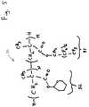
- An exemplary polymer component for the photoresist 42includes the polymer molecule 30 shown in FIG. 5.
- the polymer molecule 30is a chain that includes M units of nonpolar fluorinated monomers 31 and N units of acid-sensitive monomers 32 .
- the integers N and Mare typically in the range of 10-1000 so that the polymer molecule 30 is soluble in nonpolar solvents.
- the fluorinated monomers 31increase the solubility of the polymer molecule 30 in nonpolar solvents like fluid and supercritical carbon dioxide.
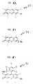
- An exemplary dye component for the photoresist 42includes one of the dye molecules 33 , 34 , 35 shown in FIGS. 6 A- 6 C.
- the dye molecules 33 , 34are activated by visible light having wavelengths of about 535 nanometers (nm) and 470 nm, respectively. These dye molecules 33 , 34 are available from Spectra Group Limited, Inc., 1722 Indian Wood Circle, Suite H Maumee, Ohio 43537 USA, under respective product names HNu-535 and HNu-470.
- the dye molecule 35is activated by light with a wavelength of about 560 nm.
- the dye moleculeis known as Rose Bengal and is available from Aldrich Company, P. O. Box 2060, Milwaukee, Wis. 53201 USA.
- An exemplary PAG component for the photoresist 42includes one of the molecules 36 , 37 as shown in FIGS. 7 A- 7 B.
- the PAG molecule 36is available from Sartomer Inc., Oaklands Corporate Center, 502 Thomas Jones Way Exton, Pa. 19341 USA, under the product name SarCat® SR1012.
- the PAGM 37is available from UCB Chemicals Corp., 2000 Lake Park Drive, Smyrna (Atlanta), Ga. 30080 USA, under the product name OPPI.
- Exemplary solvents for the photoresist 42include hydrocarbons, fluorinated hydrocarbons, and liquid and supercritical carbon dioxide.
- the fabrication process 40includes exposing the photoresist 42 to a light pattern 50 (step 12 ).
- the light patternproduces an array of illuminated regions 45 in the photoresist 42 .
- a photoreaction sequenceproduces acid.
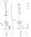
- FIG. 8shows the photoreaction sequence 38 that occurs in illuminated regions 45 of the photoresist 42 .
- photonsexcite dye molecules (DYE*), which then excite PAG molecules (Ar 2 I + X ⁇ ).
- the excited PAG molecules Ar 2 I + X ⁇ *subsequently dissociate to produce free radicals Ar-I ⁇ and Ar ⁇ X ⁇ .
- the free radicals Ar-I + ⁇react with solvent molecules (Sol-H) to produce hydronium ions H + .
- the photoreaction sequence 38is also described in the above-referenced '017 patent application.
- the photoreaction sequence 38does not produce changes to the refractive index in the illuminated regions 45 of the photoresist 49 .
- the light patterndoes not produce feedback, which could otherwise interfere with formation of the light pattern in the photoresist 42 .
- the exposurecan be performed over an extended time period and produce an acid pattern that tracks a selected light pattern.
- the fabrication process 40includes baking the photoresist 42 to cause a reaction that changes the solubility of polymer molecules that are located in the previously illuminated regions 45 of the photoresist 42 (step 14 ).
- Photo-produced acidcatalyzes the reaction, which generates polar functional groups on the polymer molecules located in the regions 45 .
- the polar functional groupsmake the reacted polymer molecules of the baked photoresist 43 less soluble in nonpolar solvents.
- FIG. 9shows an exemplary solubility changing reaction for the polymer molecule 30 shown in FIG. 5.
- the reactionis driven by H + ions and generates polar carboxylic acid groups, i.e., —CO 2 H groups, on the polymer molecules. Due to the carboxylic acid groups, the reacted polymer molecules 39 have lower solubilities in fluid or supercritical carbon dioxide.
- the fabrication process 40includes producing a void-filled template 47 by washing the baked photoresist 43 with a solvent that selectively solvates nonpolar polymer molecules (step 16 ).
- the washing stepinvolves placing the photoresist 43 and supporting substrate 44 in a cell and filling the cell with liquid or supercritical carbon dioxide.
- the liquid or supercritical carbon dioxidediffuses into the photoresist 43 to replace the nonpolar solvent therein without causing drying. Since liquid or supercritical carbon dioxide is a nonpolar solvent, the diffusing carbon dioxide dissolves nonpolar, unreacted, polymer molecules without dissolving the polar, reacted, polymer molecules.
- the diffusion of the carbon dioxideselectively removes the unreacted polymer molecules to produce a void-filled template 47 . Since the nonpolar polymer molecules are located outside of the previously illuminated regions 45 , the template 47 is a negative tone structure.
- the fabrication process 40includes raising the pressure and temperature in the cell to values corresponding to the critical point of carbon dioxide. At the critical point conditions, the carbon dioxide is allowed to diffuse out of the template 47 thereby drying the template 47 . The drying does not produce internal stresses, which could otherwise cause cracks, because critical carbon dioxide is a surface tension free fluid. Drying the template 47 in critical carbon dioxide minimizes the risk of damage due to internal surface tension forces.
- the fabrication process 40includes filling voids in the template 47 with a high refractive index material (step 22 ).
- the filling stepis performed at a temperature below 350° C. and preferably below about 300° C. to avoid damaging polymer molecules, cross-linking of polymer molecules, or damaging the high refractive index material.
- the filling stepproduces filled structure 48 , which includes non-crosslinked polymer molecules in regions 45 and high refractive index material elsewhere.
- Exemplary fill stepsinclude melting a high refractive index material with a low melting temperature, e.g., selenium or bismuth, and filling the melted material into the voids of the template 47 under pressure.
- Other exemplary fill stepsinclude subliming a high refractive index material having a low vaporization temperature into the voids of the template 47 .
- Other exemplary fill stepsinclude performing a gas-phase reaction that deposits a high refractive index byproduct in the voids of the template 47 .
- the fabrication process 40also includes washing the filled structure 48 to dissolve away the polymer molecules of the original template 47 to produce a porous structure 41 of the high refractive index material and then drying the structure (steps 24 and 26 ).
- the washing stepproduces a porous structure of the high refractive index material alone.
- a basic aqueous solutionis a suitable solution for the washing step.
- FIG. 4illustrates the alternate process 40 ′ for fabricating porous structure 41 ′ of high index material.
- the process 40 ′includes performing steps 12 and 14 to produce the baked photoresist 43 as already described with respect to process 40 of FIG. 3.
- the reacted polymer molecules in regions 45are insoluble in a nonpolar solvent.
- the reacted polymer molecule 39 of FIG. 8is insoluble in nonpolar solvents due to the polar carboxylic acid groups produced by the chemical reaction of step 14 .
- the process 40 ′includes performing a vapor-phase reaction to change the solubility of a portion of the polymer molecules of the photoresist 43 .
- the vapor-phase reactionproduces a photoresist 43 ′ in which the polymer molecules located in the regions 45 have a changed solubility.
- the reactioncauses these previously reacted polymer molecules to become more soluble in nonpolar solvents such as liquid or supercritical carbon dioxide.
- FIG. 10shows an exemplary vapor-phase reaction for changing the solubility of the polymer molecule 39 of FIG. 9.
- the reactionis a hydrosilylation in which (CH 3 ) 3 SiOSi(CH 3 ) 3 (HMDS) reacts with carboxylic acid groups on the polymer molecule 39 to produce less polar functional groups.
- the hydrosilylation reactionchanges the solubility of the previously reacted polymer molecules.
- the reactioncaps the polar carboxylic acid groups to make molecule 39 ′ significantly more soluble in nonpolar solvents than the original molecule 39 .
- the process 40 ′includes uniformly illuminating the photoresist 43 ′ to generate acid in regions 46 via the photo-reaction sequence 38 of FIG. 8. Then, a rebake step causes the photo-produced acid to catalyze a reaction in the polymer molecules that are located in the regions 46 of the photoresist 43 ′′. The reaction changes the solubility of said polymer molecules, which were not previously exposed by the nontrivial light pattern. From the exemplary nonpolar polymer molecules 30 , shown in FIG. 9, the rebake produces the polar molecules 39 . The rebake does not crosslink polymer molecules or cause hydrosilylated polymer molecules in the previously reacted regions 45 of the photoresist 43 ′ to further react.
- the process 40 ′also includes producing a void-filled polymer template 47 ′ by washing the rebaked photoresist 43 ′′ with fluid or supercritical carbon dioxide as already described with respect to above process 40 (step 16 ).
- the washdissolves away the nonpolar polymer molecules that located in regions 45 thereby producing a positive tone structure in polymer template 47 ′.
- Combining the vapor-phase reaction, uniform illumination, and rebakeinverted the spatial distribution of molecules soluble in polar and nonpolar solvents, respectively, to produce a positive tone template 47 ′ rather than the negative tone template 47 of FIG. 3.
- the fabrication process 40 ′also includes filling voids in the template 47 ′ with a high refractive index material to produce filled structure 48 ′ in a manner already described with respect to process 40 (step 22 ).
- the filled structure 48 ′is then washed with a solvent that solvates the non-crosslinked polymer molecules of the template 47 ′ to produce the porous structure of the high refractive index material (step 24 ).
- the porous structureis dried to produce the final void-filled structure 41 ′ of the high refractive index material (step 26 ).
- the final void-filled structure 41 ′ of the high refractive index materialis a positive tone structure.
Landscapes
- Physics & Mathematics (AREA)
- General Physics & Mathematics (AREA)
- Spectroscopy & Molecular Physics (AREA)
- Chemical & Material Sciences (AREA)
- Chemical Kinetics & Catalysis (AREA)
- Inorganic Chemistry (AREA)
- Organic Chemistry (AREA)
- Optical Integrated Circuits (AREA)
Abstract
Description
- 1. Field of the Invention[0001]
- The invention relates to structures with artificially patterned refractive indexes.[0002]
- 2. Discussion of the Related Art[0003]
- A photonic crystal is a material with a refractive index that varies periodically. In a photonic crystal, the optical response results from a coherent superposition of optical waves propagating therein. Photonic crystals with sufficiently high refractive index contrasts, e.g., a contrast of more than 2, exhibit complete photonic bandgaps. A photonic bandgap prohibits electromagnetic waves from propagating in such a crystal for wave vectors at optical wavelengths.[0004]
- Herein, a photonic crystal with a complete photonic bandgap will be referred to as a photonic bandgap structure. Photonic bandgap structures have applications in a variety of optical devices. Thus, processes for fabricating such structures are useful.[0005]
- One process for fabricating a photonic bandgap structure involves producing a periodic array of voids in a base material. In such a void-filled photonic bandgap structure, the refractive index pattern has a high contrast if the base material has a high refractive index.[0006]
- Fabricating a void-filled structure from a material with a high refractive index typically involves a multi-step template-based process. First, a reaction step produces a template with a periodic array of voids therein. Second, a fill step introduces a material with a high refractive index into the voids of the template. Third, a removal step eliminates the template material from the filled structure to produce a porous structure of the high refractive index material alone.[0007]
- Such template-based fabrication processes need to account for the properties of both the template material and the filling material. In particular, the filling step must not damage the template material, and the removal step must not damage the filling material. Unfortunately, many photoresists do not withstand the process of being filled with a material having a high refractive index. Similarly, many high refractive index materials do not withstand the treatments for removing templates made of photoresists.[0008]
- Various embodiments provide polymer templates and processes for fabricating the polymer templates. The polymer templates enable fabrication of porous structures from materials with high refractive indexes. In particular, the template material is compatible with being filled with a high refractive index material, and removal of the template material from the resulting structure is possible without damaging the high refractive index material. Both the filling and removal steps are typically performed at low temperatures to avoid damage to the various materials.[0009]
- In one aspect, the invention features a process for forming a polymer template. The process includes exposing a photoresist including polymer molecules to a light pattern and baking the photoresist to chemically react polymer molecules in portions of the photoresist that were exposed to light of the light pattern. The reacted polymer molecules have a different solubility in a solvent than chemically unreacted polymer molecules. The process also includes washing the baked photoresist with the solvent to produce voids therein by selectively dissolving away either the reacted polymer molecules or the unreacted polymer molecules.[0010]
- In another aspect, the invention features a process for forming a template of non-crosslinked polymer molecules. The process includes exposing a polymer photoresist to a light pattern to generate acid in illuminated regions of the photoresist and baking the photoresist to cause polymer molecules that are located in the illuminated regions to react with the acid. The baking step does not crosslink the polymer molecules. The process includes washing the baked photoresist in a nonpolar solvent to produce voids therein by selectively solvating either the reacted polymer molecules or the unreacted polymer molecules.[0011]
- Herein, various processes involving exposure of a material to a light pattern with light and dark regions produce a void-filled structure. The resulting structures are referred to as positive tone structures if the voids occupy regions that were exposed to light regions of the light pattern. The resulting structures are referred to as negative tone structures if the voids occupy regions that were dark regions of the light pattern.[0012]
- FIG. 1 is flow chart showing a process for fabricating a porous template of non-crosslinked polymer molecules;[0013]
- FIG. 2 is flow chart showing a process for fabricating a porous structure of a of a high refractive index material from the template of FIG. 1;[0014]
- FIG. 3 illustrates a process that fabricates a porous structure of a high refractive index material by fabricating a negative tone polymer template;[0015]
- FIG. 4 illustrates a process that fabricates a porous structure of a high refractive index material by fabricating a positive tone polymer template;[0016]
- FIG. 5 shows an exemplary polymer molecule for the polymer photoresist used in the processes of FIGS.[0017]3-4;
- FIGS.[0018]6A-6C show exemplary dye molecules for the polymer photoresist used in the processes of FIGS.3-4;
- FIGS.[0019]7A-7B show exemplary PAG molecules for the polymer photoresist used in the processes of FIGS.3-4;
- FIG. 8 illustrates the sequence of photoreactions in exemplary photoresists used in the processes of FIGS.[0020]3-4;
- FIG. 9 shows an acid-catalyzed reaction of polymer molecules in the processes of FIGS.[0021]3-4; and
- FIG. 10 shows a reaction that changes the solubility of polymer molecules previously modified by the acid-catalyzed reaction shown in FIG. 9.[0022]
- In the various Figures, like reference numbers indicate elements with similar functions.[0023]
- FIG. 1 illustrates a[0024]
process 10 for fabricating a template from a polymer photoresist. The template is a homogeneous material of non-crosslinked polymer molecules with a pattern of voids therein. The voids of exemplary templates form periodic patterns in one-, two-, or three-dimensions. - The[0025]
process 10 includes exposing a slab of photoresist to a light pattern to produce a corresponding pattern of acid in the photoresist (step12). The photoresist is a homogenous mixture of polymer molecules, dye molecules, and photoacid generator molecules. The light of the exposure causes the photo-acid generator molecules to produce acid, i.e., hydronium ions (H+). The distribution of H+ ions corresponds to the light intensity pattern during the exposure. - Herein, a light pattern includes both an array of dark regions and an array of light regions. Exemplary light patterns are periodic in one, two, or three dimensions and have periods of about 0.1 microns and about 10 microns, i.e., mesoscopic scale periods suitable for photonic bandgap structures at telecommunications wavelengths. Such periodic light patterns result from interfering two, three, or four mutually coherent light beams. Processes for producing such light patterns are described in pending U.S. patent application Ser. No. 10/040,017, filed Jan. 4, 2002, ('017), which is incorporated herein by reference in its entirety.[0026]
- The light exposure does not stimulate chemical reactions that significantly change the refractive index of the photoresist. In particular, the photochemical reactions do not polymerize, decompose, or crosslink molecules in the photoresist. Instead, the photochemical reactions produce acid, which does not significantly change the refractive index. The absence of refractive index changes insures that the light patterning will not lead to material changes that feedback and could otherwise interfere with the acid pattern formed in the photoresist. The final acid distribution forms a pattern that corresponds to the light pattern used to expose the photoresist.[0027]
- The[0028]
process 10 includes baking the exposed photoresist to cause polymer molecules, which are located in regions exposed by the light, to undergo a solubility change (step14). In some embodiments, the solubility change results from generation of polar groups on the polymer molecules. In other embodiments, the solubility change results from generation of nonpolar groups on the polymer molecules. The new groups are generated by a heat-induced reaction of polymer molecules that are located in portions of the photoresist where acid was generated during the light patterning. The acid catalyzes the reaction. - The bake step proceeds at a temperature that is above the glass transition temperature of the organic polymer molecules of the photoresist and is lower than the decomposition temperature for the molecules. Exemplary bake temperatures for polymer resists are below about 350° C. and are preferably below about 200° C.[0029]
- Various embodiments of the[0030]
process 10 use a photoresist whose polymer molecules are initially soluble in a nonpolar solvent. For polymer molecules initially soluble in a nonpolar solvent, the acid-catalyzed reaction produces polymer molecules with more polar functional groups. The reacted polymer molecules are thus, less soluble in the nonpolar solvent and more soluble in polar solvents. After the bake, the photoresist includes a pattern of polymer molecule solubility type that tracks the light pattern used during the exposure atstep 12. - In some embodiments, further chemical treatments invert the solubilities of polymer molecules located in respective light and dark regions of the light pattern as described below.[0031]
- The[0032]
process 10 also includes washing the baked photoresist with solvent to produce voids therein by selectively dissolving away polymer molecules of one solubility type (step16). Exemplary washes use a nonpolar liquid as the solvent. In such solvents, the unreacted and reacted polymer molecules of the baked photoresist have different solubilities. For that reason, the wash generates a pattern of voids that tracks the light pattern originally used to exposure the photoresist. The resulting void-filled photoresist is a polymer template. - To enable the wash to produce voids, the conditions of the bake are selected to not crosslink polymer molecules. Crosslinking would significantly lower solubilities of the polymer molecules and would impede a solvent from removing the polymer template after subsequent filling with high index materials.[0033]
- FIG. 2 illustrates a[0034]
process 18 for fabricating a porous structure of a high refractive index material. Theprocess 18 includes providing a void filled template of non-crosslinked polymer molecules, e.g., a template fabricated byprocess 10 of FIG. 1 (step20). Theprocess 18 includes forming a filled structure by filling the voids of the template with a high refractive index material (step22). The filling is performed under low temperature conditions that neither damage the template nor crosslink polymer molecules of the template. Exemplary filling temperatures are below about 350° C. Next, theprocess 18 includes washing the structure with a solvent that solvates polymer molecules of the template (step24). The solvated polymer molecules are washed away to produce a void-filled structure of the high refractive index material alone. Finally, the porous structure of the high refractive index material is dried to remove remaining solvent from the voids therein (step26). - FIGS. 3 and 4 illustrate[0035]
specific embodiments porous structures processes porous structures Exemplary structures - Processes[0036]40 and40′ start with a layer of
photoresist 42. The photoresist is supported on asubstrate 44, e.g., a glass substrate. Thephotoresist 42 is a homogeneous mixture whose components include soluble polymer molecules, dye molecules, photoacid generator (PAG) molecules, and solvent. Exemplary components for thephotoresist 42 are shown in FIGS.5,6A-6C, and7A-7B. - An exemplary polymer component for the[0037]
photoresist 42 includes thepolymer molecule 30 shown in FIG. 5. Thepolymer molecule 30 is a chain that includes M units of nonpolarfluorinated monomers 31 and N units of acid-sensitive monomers 32. The integers N and M are typically in the range of 10-1000 so that thepolymer molecule 30 is soluble in nonpolar solvents. Thefluorinated monomers 31 increase the solubility of thepolymer molecule 30 in nonpolar solvents like fluid and supercritical carbon dioxide. - An exemplary dye component for the[0038]
photoresist 42 includes one of thedye molecules 33,34,35 shown in FIGS.6A-6C. Thedye molecules 33,34 are activated by visible light having wavelengths of about 535 nanometers (nm) and 470 nm, respectively. Thesedye molecules 33,34 are available from Spectra Group Limited, Inc., 1722 Indian Wood Circle, Suite H Maumee, Ohio 43537 USA, under respective product names HNu-535 and HNu-470. The dye molecule35 is activated by light with a wavelength of about 560 nm. The dye molecule is known as Rose Bengal and is available from Aldrich Company, P. O. Box 2060, Milwaukee, Wis. 53201 USA. - An exemplary PAG component for the[0039]
photoresist 42 includes one of themolecules PAG molecule 36 is available from Sartomer Inc., Oaklands Corporate Center, 502 Thomas Jones Way Exton, Pa. 19341 USA, under the product name SarCat® SR1012. ThePAGM 37 is available from UCB Chemicals Corp., 2000 Lake Park Drive, Smyrna (Atlanta), Ga. 30080 USA, under the product name OPPI. - Exemplary solvents for the[0040]
photoresist 42 include hydrocarbons, fluorinated hydrocarbons, and liquid and supercritical carbon dioxide. - Referring to FIG. 3, the[0041]
fabrication process 40 includes exposing thephotoresist 42 to a light pattern50 (step12). The light pattern produces an array ofilluminated regions 45 in thephotoresist 42. In theilluminated regions 45, a photoreaction sequence produces acid. - FIG. 8 shows the[0042]
photoreaction sequence 38 that occurs inilluminated regions 45 of thephotoresist 42. In thephotoreaction sequence 38, photons excite dye molecules (DYE*), which then excite PAG molecules (Ar2I+ X−). The excited PAG molecules Ar2I+ X−*subsequently dissociate to produce free radicals Ar-I−· and Ar·X−. The free radicals Ar-I+· react with solvent molecules (Sol-H) to produce hydronium ions H+. Thephotoreaction sequence 38 is also described in the above-referenced '017 patent application. - The[0043]
photoreaction sequence 38 does not produce changes to the refractive index in theilluminated regions 45 of the photoresist49. Thus, the light pattern does not produce feedback, which could otherwise interfere with formation of the light pattern in thephotoresist 42. For this reason, the exposure can be performed over an extended time period and produce an acid pattern that tracks a selected light pattern. - Referring again to FIG. 3, the[0044]
fabrication process 40 includes baking thephotoresist 42 to cause a reaction that changes the solubility of polymer molecules that are located in the previously illuminatedregions 45 of the photoresist42 (step14). Photo-produced acid catalyzes the reaction, which generates polar functional groups on the polymer molecules located in theregions 45. The polar functional groups make the reacted polymer molecules of thebaked photoresist 43 less soluble in nonpolar solvents. - FIG. 9 shows an exemplary solubility changing reaction for the[0045]
polymer molecule 30 shown in FIG. 5. The reaction is driven by H+ ions and generates polar carboxylic acid groups, i.e., —CO2H groups, on the polymer molecules. Due to the carboxylic acid groups, the reactedpolymer molecules 39 have lower solubilities in fluid or supercritical carbon dioxide. - Referring again to FIG. 3, the[0046]
fabrication process 40 includes producing a void-filledtemplate 47 by washing thebaked photoresist 43 with a solvent that selectively solvates nonpolar polymer molecules (step16). The washing step involves placing thephotoresist 43 and supportingsubstrate 44 in a cell and filling the cell with liquid or supercritical carbon dioxide. The liquid or supercritical carbon dioxide diffuses into thephotoresist 43 to replace the nonpolar solvent therein without causing drying. Since liquid or supercritical carbon dioxide is a nonpolar solvent, the diffusing carbon dioxide dissolves nonpolar, unreacted, polymer molecules without dissolving the polar, reacted, polymer molecules. Thus, the diffusion of the carbon dioxide selectively removes the unreacted polymer molecules to produce a void-filledtemplate 47. Since the nonpolar polymer molecules are located outside of the previously illuminatedregions 45, thetemplate 47 is a negative tone structure. - The[0047]
fabrication process 40 includes raising the pressure and temperature in the cell to values corresponding to the critical point of carbon dioxide. At the critical point conditions, the carbon dioxide is allowed to diffuse out of thetemplate 47 thereby drying thetemplate 47. The drying does not produce internal stresses, which could otherwise cause cracks, because critical carbon dioxide is a surface tension free fluid. Drying thetemplate 47 in critical carbon dioxide minimizes the risk of damage due to internal surface tension forces. - The[0048]
fabrication process 40 includes filling voids in thetemplate 47 with a high refractive index material (step22). The filling step is performed at a temperature below 350° C. and preferably below about 300° C. to avoid damaging polymer molecules, cross-linking of polymer molecules, or damaging the high refractive index material. The filling step produces filledstructure 48, which includes non-crosslinked polymer molecules inregions 45 and high refractive index material elsewhere. - A variety of processes are available to fill the voids of the[0049]
template 47 with a high refractive index material. Exemplary fill steps include melting a high refractive index material with a low melting temperature, e.g., selenium or bismuth, and filling the melted material into the voids of thetemplate 47 under pressure. Other exemplary fill steps include subliming a high refractive index material having a low vaporization temperature into the voids of thetemplate 47. Other exemplary fill steps include performing a gas-phase reaction that deposits a high refractive index byproduct in the voids of thetemplate 47. - The[0050]
fabrication process 40 also includes washing the filledstructure 48 to dissolve away the polymer molecules of theoriginal template 47 to produce aporous structure 41 of the high refractive index material and then drying the structure (steps 24 and26). The washing step produces a porous structure of the high refractive index material alone. For thepolar polymer molecules 39 shown in FIG. 7, a basic aqueous solution is a suitable solution for the washing step. - FIG. 4 illustrates the[0051]
alternate process 40′ for fabricatingporous structure 41′ of high index material. Theprocess 40′ includes performingsteps baked photoresist 43 as already described with respect to process40 of FIG. 3. In thebaked photoresist 43, the reacted polymer molecules inregions 45 are insoluble in a nonpolar solvent. As an example, the reactedpolymer molecule 39 of FIG. 8 is insoluble in nonpolar solvents due to the polar carboxylic acid groups produced by the chemical reaction ofstep 14. - The[0052]
process 40′ includes performing a vapor-phase reaction to change the solubility of a portion of the polymer molecules of thephotoresist 43. The vapor-phase reaction produces aphotoresist 43′ in which the polymer molecules located in theregions 45 have a changed solubility. The reaction causes these previously reacted polymer molecules to become more soluble in nonpolar solvents such as liquid or supercritical carbon dioxide. - FIG. 10 shows an exemplary vapor-phase reaction for changing the solubility of the[0053]
polymer molecule 39 of FIG. 9. The reaction is a hydrosilylation in which (CH3)3SiOSi(CH3)3(HMDS) reacts with carboxylic acid groups on thepolymer molecule 39 to produce less polar functional groups. The hydrosilylation reaction changes the solubility of the previously reacted polymer molecules. In particular, the reaction caps the polar carboxylic acid groups to makemolecule 39′ significantly more soluble in nonpolar solvents than theoriginal molecule 39. - Referring again to FIG. 4, the[0054]
process 40′ includes uniformly illuminating thephotoresist 43′ to generate acid inregions 46 via the photo-reaction sequence 38 of FIG. 8. Then, a rebake step causes the photo-produced acid to catalyze a reaction in the polymer molecules that are located in theregions 46 of thephotoresist 43″. The reaction changes the solubility of said polymer molecules, which were not previously exposed by the nontrivial light pattern. From the exemplarynonpolar polymer molecules 30, shown in FIG. 9, the rebake produces thepolar molecules 39. The rebake does not crosslink polymer molecules or cause hydrosilylated polymer molecules in the previously reactedregions 45 of thephotoresist 43′ to further react. - The[0055]
process 40′ also includes producing a void-filledpolymer template 47′ by washing therebaked photoresist 43″ with fluid or supercritical carbon dioxide as already described with respect to above process40 (step16). The wash dissolves away the nonpolar polymer molecules that located inregions 45 thereby producing a positive tone structure inpolymer template 47′. Combining the vapor-phase reaction, uniform illumination, and rebake inverted the spatial distribution of molecules soluble in polar and nonpolar solvents, respectively, to produce apositive tone template 47′ rather than thenegative tone template 47 of FIG. 3. - The[0056]
fabrication process 40′ also includes filling voids in thetemplate 47′ with a high refractive index material to produce filledstructure 48′ in a manner already described with respect to process40 (step22). The filledstructure 48′ is then washed with a solvent that solvates the non-crosslinked polymer molecules of thetemplate 47′ to produce the porous structure of the high refractive index material (step24). - The porous structure is dried to produce the final void-filled[0057]
structure 41′ of the high refractive index material (step26). The final void-filledstructure 41′ of the high refractive index material is a positive tone structure. - From the disclosure, drawings, and claims, other embodiments of the invention will be apparent to those skilled in the art.[0058]
Claims (18)
Priority Applications (2)
| Application Number | Priority Date | Filing Date | Title |
|---|---|---|---|
| US10/321,027US7008757B2 (en) | 2002-12-17 | 2002-12-17 | Patterned structures of high refractive index materials |
| US11/316,058US20060099536A1 (en) | 2002-12-17 | 2005-12-21 | Patterned structures of high refractive index materials |
Applications Claiming Priority (1)
| Application Number | Priority Date | Filing Date | Title |
|---|---|---|---|
| US10/321,027US7008757B2 (en) | 2002-12-17 | 2002-12-17 | Patterned structures of high refractive index materials |
Related Child Applications (1)
| Application Number | Title | Priority Date | Filing Date |
|---|---|---|---|
| US11/316,058ContinuationUS20060099536A1 (en) | 2002-12-17 | 2005-12-21 | Patterned structures of high refractive index materials |
Publications (2)
| Publication Number | Publication Date |
|---|---|
| US20040115566A1true US20040115566A1 (en) | 2004-06-17 |
| US7008757B2 US7008757B2 (en) | 2006-03-07 |
Family
ID=32507021
Family Applications (2)
| Application Number | Title | Priority Date | Filing Date |
|---|---|---|---|
| US10/321,027Expired - LifetimeUS7008757B2 (en) | 2002-12-17 | 2002-12-17 | Patterned structures of high refractive index materials |
| US11/316,058AbandonedUS20060099536A1 (en) | 2002-12-17 | 2005-12-21 | Patterned structures of high refractive index materials |
Family Applications After (1)
| Application Number | Title | Priority Date | Filing Date |
|---|---|---|---|
| US11/316,058AbandonedUS20060099536A1 (en) | 2002-12-17 | 2005-12-21 | Patterned structures of high refractive index materials |
Country Status (1)
| Country | Link |
|---|---|
| US (2) | US7008757B2 (en) |
Cited By (5)
| Publication number | Priority date | Publication date | Assignee | Title |
|---|---|---|---|---|
| US20040172973A1 (en)* | 2003-03-06 | 2004-09-09 | Lucent Technologies, Inc. | Process for making crystalline structures having interconnected pores and high refractive index contrasts |
| EP2435194A1 (en)* | 2009-05-26 | 2012-04-04 | Debiotech S.A. | Controlling the porosity in an anisotropic coating |
| US11173649B1 (en) | 2018-12-11 | 2021-11-16 | Facebook Technologies, Llc | Reducing adhesive failure during nanoimprint lithography demolding |
| US11262650B1 (en) | 2018-12-11 | 2022-03-01 | Facebook Technologies, Llc | Reducing adhesive failure during nanoimprint lithography demolding |
| US11294278B1 (en) | 2018-12-11 | 2022-04-05 | Facebook Technologies, Llc | Reducing adhesive failure during nanoimprint lithography demolding |
Families Citing this family (10)
| Publication number | Priority date | Publication date | Assignee | Title |
|---|---|---|---|---|
| US7106519B2 (en)* | 2003-07-31 | 2006-09-12 | Lucent Technologies Inc. | Tunable micro-lens arrays |
| ATE439612T1 (en)* | 2003-12-05 | 2009-08-15 | 3M Innovative Properties Co | PROCESS FOR MAKING PHOTONIC CRYSTALS |
| US20050124712A1 (en)* | 2003-12-05 | 2005-06-09 | 3M Innovative Properties Company | Process for producing photonic crystals |
| CN101080672A (en)* | 2004-12-14 | 2007-11-28 | 荷兰聚合物研究所 | Porous holographic film |
| US8734003B2 (en)* | 2005-09-15 | 2014-05-27 | Alcatel Lucent | Micro-chemical mixing |
| US8721161B2 (en) | 2005-09-15 | 2014-05-13 | Alcatel Lucent | Fluid oscillations on structured surfaces |
| US8623458B2 (en)* | 2009-12-18 | 2014-01-07 | International Business Machines Corporation | Methods of directed self-assembly, and layered structures formed therefrom |
| US8821978B2 (en)* | 2009-12-18 | 2014-09-02 | International Business Machines Corporation | Methods of directed self-assembly and layered structures formed therefrom |
| US8828493B2 (en)* | 2009-12-18 | 2014-09-09 | International Business Machines Corporation | Methods of directed self-assembly and layered structures formed therefrom |
| CN102279518B (en)* | 2011-06-12 | 2012-08-08 | 华北电力大学(保定) | Method for manufacturing metal doped full space or quasi-full space photonic crystal |
Citations (17)
| Publication number | Priority date | Publication date | Assignee | Title |
|---|---|---|---|---|
| US5239412A (en)* | 1990-02-05 | 1993-08-24 | Sharp Kabushiki Kaisha | Solid image pickup device having microlenses |
| US5248734A (en)* | 1992-06-16 | 1993-09-28 | Cornell Research Foundation, Inc. | Process for preparing a polyphenylene polymer |
| US5324623A (en)* | 1991-06-04 | 1994-06-28 | Sony Corporation | Microlens forming method |
| US5348687A (en)* | 1993-11-26 | 1994-09-20 | Mobil Oil Corp. | M41S materials having nonlinear optical properties |
| US5665527A (en)* | 1995-02-17 | 1997-09-09 | International Business Machines Corporation | Process for generating negative tone resist images utilizing carbon dioxide critical fluid |
| US5922299A (en)* | 1996-11-26 | 1999-07-13 | Battelle Memorial Institute | Mesoporous-silica films, fibers, and powders by evaporation |
| US5948470A (en)* | 1997-04-28 | 1999-09-07 | Harrison; Christopher | Method of nanoscale patterning and products made thereby |
| US6027666A (en)* | 1998-06-05 | 2000-02-22 | The Governing Council Of The University Of Toronto | Fast luminescent silicon |
| US6042998A (en)* | 1993-09-30 | 2000-03-28 | The University Of New Mexico | Method and apparatus for extending spatial frequencies in photolithography images |
| US6136505A (en)* | 1998-06-12 | 2000-10-24 | Tokyo Ohka Kogyo Co., Ltd. | Liquid coating composition for use in forming antireflective film and photoresist material using said antireflective film |
| US6329070B1 (en)* | 1999-12-09 | 2001-12-11 | Cornell Research Foundation, Inc. | Fabrication of periodic surface structures with nanometer-scale spacings |
| US6379874B1 (en)* | 1999-10-26 | 2002-04-30 | Cornell Research Foundation, Inc. | Using block copolymers as supercritical fluid developable photoresists |
| US6387453B1 (en)* | 2000-03-02 | 2002-05-14 | Sandia Corporation | Method for making surfactant-templated thin films |
| US6409907B1 (en)* | 1999-02-11 | 2002-06-25 | Lucent Technologies Inc. | Electrochemical process for fabricating article exhibiting substantial three-dimensional order and resultant article |
| US6465387B1 (en)* | 1999-08-12 | 2002-10-15 | Board Of Trustees Of Michigan State University | Combined porous organic and inorganic oxide materials prepared by non-ionic surfactant templating route |
| US6471761B2 (en)* | 2000-04-21 | 2002-10-29 | University Of New Mexico | Prototyping of patterned functional nanostructures |
| US20040023150A1 (en)* | 1998-09-23 | 2004-02-05 | Feiring Andrew E. | Photoresists, polymers and processes for microlithography |
Family Cites Families (4)
| Publication number | Priority date | Publication date | Assignee | Title |
|---|---|---|---|---|
| US629070A (en)* | 1896-12-15 | 1899-07-18 | Pompeo Garuti | Apparatus for producing oxygen and hydrogen. |
| US5248934A (en)* | 1992-01-10 | 1993-09-28 | Roveti Denes K | Method and apparatus for converting a conventional DC multimeter to an AC impedance meter |
| US6509138B2 (en) | 2000-01-12 | 2003-01-21 | Semiconductor Research Corporation | Solventless, resistless direct dielectric patterning |
| US7168266B2 (en)* | 2003-03-06 | 2007-01-30 | Lucent Technologies Inc. | Process for making crystalline structures having interconnected pores and high refractive index contrasts |
- 2002
- 2002-12-17USUS10/321,027patent/US7008757B2/ennot_activeExpired - Lifetime
- 2005
- 2005-12-21USUS11/316,058patent/US20060099536A1/ennot_activeAbandoned
Patent Citations (18)
| Publication number | Priority date | Publication date | Assignee | Title |
|---|---|---|---|---|
| US5239412A (en)* | 1990-02-05 | 1993-08-24 | Sharp Kabushiki Kaisha | Solid image pickup device having microlenses |
| US5324623A (en)* | 1991-06-04 | 1994-06-28 | Sony Corporation | Microlens forming method |
| US5248734A (en)* | 1992-06-16 | 1993-09-28 | Cornell Research Foundation, Inc. | Process for preparing a polyphenylene polymer |
| US6042998A (en)* | 1993-09-30 | 2000-03-28 | The University Of New Mexico | Method and apparatus for extending spatial frequencies in photolithography images |
| US5348687A (en)* | 1993-11-26 | 1994-09-20 | Mobil Oil Corp. | M41S materials having nonlinear optical properties |
| US5665527A (en)* | 1995-02-17 | 1997-09-09 | International Business Machines Corporation | Process for generating negative tone resist images utilizing carbon dioxide critical fluid |
| US5922299A (en)* | 1996-11-26 | 1999-07-13 | Battelle Memorial Institute | Mesoporous-silica films, fibers, and powders by evaporation |
| US5948470A (en)* | 1997-04-28 | 1999-09-07 | Harrison; Christopher | Method of nanoscale patterning and products made thereby |
| US6027666A (en)* | 1998-06-05 | 2000-02-22 | The Governing Council Of The University Of Toronto | Fast luminescent silicon |
| US6319427B1 (en)* | 1998-06-05 | 2001-11-20 | Geoffrey A. Ozin | Fast luminescent silicon |
| US6136505A (en)* | 1998-06-12 | 2000-10-24 | Tokyo Ohka Kogyo Co., Ltd. | Liquid coating composition for use in forming antireflective film and photoresist material using said antireflective film |
| US20040023150A1 (en)* | 1998-09-23 | 2004-02-05 | Feiring Andrew E. | Photoresists, polymers and processes for microlithography |
| US6409907B1 (en)* | 1999-02-11 | 2002-06-25 | Lucent Technologies Inc. | Electrochemical process for fabricating article exhibiting substantial three-dimensional order and resultant article |
| US6465387B1 (en)* | 1999-08-12 | 2002-10-15 | Board Of Trustees Of Michigan State University | Combined porous organic and inorganic oxide materials prepared by non-ionic surfactant templating route |
| US6379874B1 (en)* | 1999-10-26 | 2002-04-30 | Cornell Research Foundation, Inc. | Using block copolymers as supercritical fluid developable photoresists |
| US6329070B1 (en)* | 1999-12-09 | 2001-12-11 | Cornell Research Foundation, Inc. | Fabrication of periodic surface structures with nanometer-scale spacings |
| US6387453B1 (en)* | 2000-03-02 | 2002-05-14 | Sandia Corporation | Method for making surfactant-templated thin films |
| US6471761B2 (en)* | 2000-04-21 | 2002-10-29 | University Of New Mexico | Prototyping of patterned functional nanostructures |
Cited By (6)
| Publication number | Priority date | Publication date | Assignee | Title |
|---|---|---|---|---|
| US20040172973A1 (en)* | 2003-03-06 | 2004-09-09 | Lucent Technologies, Inc. | Process for making crystalline structures having interconnected pores and high refractive index contrasts |
| US7168266B2 (en)* | 2003-03-06 | 2007-01-30 | Lucent Technologies Inc. | Process for making crystalline structures having interconnected pores and high refractive index contrasts |
| EP2435194A1 (en)* | 2009-05-26 | 2012-04-04 | Debiotech S.A. | Controlling the porosity in an anisotropic coating |
| US11173649B1 (en) | 2018-12-11 | 2021-11-16 | Facebook Technologies, Llc | Reducing adhesive failure during nanoimprint lithography demolding |
| US11262650B1 (en) | 2018-12-11 | 2022-03-01 | Facebook Technologies, Llc | Reducing adhesive failure during nanoimprint lithography demolding |
| US11294278B1 (en) | 2018-12-11 | 2022-04-05 | Facebook Technologies, Llc | Reducing adhesive failure during nanoimprint lithography demolding |
Also Published As
| Publication number | Publication date |
|---|---|
| US7008757B2 (en) | 2006-03-07 |
| US20060099536A1 (en) | 2006-05-11 |
Similar Documents
| Publication | Publication Date | Title |
|---|---|---|
| US7008757B2 (en) | Patterned structures of high refractive index materials | |
| US5234793A (en) | Method for dimensionally accurate structure transfer in bilayer technique wherein a treating step with a bulging agent is employed after development | |
| US8841058B2 (en) | Photolithography material for immersion lithography processes | |
| US9429837B2 (en) | Aqueous curable imprintable medium and patterned layer forming method | |
| Hayase | Polysilanes for semiconductor fabrication | |
| US20070269749A1 (en) | Methods to reduce the minimum pitch in a pattern | |
| US20030129501A1 (en) | Fabricating artificial crystalline structures | |
| US9235125B2 (en) | Methods of providing patterned chemical epitaxy templates for self-assemblable block copolymers for use in device lithography | |
| US6743572B2 (en) | Method for structuring a photoresist layer | |
| KR100515369B1 (en) | Apparatus for forming fine patterns of semiconductor wafer by electric field and the method of the same | |
| EP0098922A2 (en) | Process for selectively generating positive and negative resist patterns from a single exposure pattern | |
| US20030099906A1 (en) | Process for the aromatization and cycloaliphatization of photoresists in the uv range | |
| US5275920A (en) | Method of dry development utilizing quinone diazide and basic polymer resist with latent image intensification through treatment with silicon-organic compound in water | |
| US20030124468A1 (en) | Process for silylating photoresists in the UV range | |
| Pariani et al. | Adaptable Microcontact Printing via Photochromic Optical‐Saturable Lithography | |
| JP2004191993A (en) | Conjugate polymer pattern forming composition and pattern forming method using the same | |
| US6372411B1 (en) | Polymer pattern forming method | |
| CN110501873B (en) | Photoresist and photoetching method | |
| JPH04342260A (en) | Formation of resist pattern | |
| KR19990004871A (en) | Semiconductor Device Photo Etching Process | |
| JPH07104483A (en) | Pattern formation method | |
| US20030073039A1 (en) | Method of forming a patterned photoresist with a non-distorted profile | |
| Kamon et al. | Resist cluster formation model and development simulation | |
| Richardson | The fabrication and lithography of conjugated polymer distributed feedback lasers and development of their applications | |
| KR100253084B1 (en) | Base resin for photoresist using ultra-violet ray for fabrication of semiconductor device, its manufacturing method and photoresist using ultra-violet ray comprosing the base resin |
Legal Events
| Date | Code | Title | Description |
|---|---|---|---|
| AS | Assignment | Owner name:LUCENT TECHNOLOGIES INC., NEW JERSEY Free format text:ASSIGNMENT OF ASSIGNORS INTEREST;ASSIGNORS:REICHMANIS, ELSA;YANG, SHU;REEL/FRAME:013602/0488 Effective date:20021217 | |
| STCF | Information on status: patent grant | Free format text:PATENTED CASE | |
| FEPP | Fee payment procedure | Free format text:PAYOR NUMBER ASSIGNED (ORIGINAL EVENT CODE: ASPN); ENTITY STATUS OF PATENT OWNER: LARGE ENTITY | |
| FPAY | Fee payment | Year of fee payment:4 | |
| AS | Assignment | Owner name:CREDIT SUISSE AG, NEW YORK Free format text:SECURITY INTEREST;ASSIGNOR:ALCATEL-LUCENT USA INC.;REEL/FRAME:030510/0627 Effective date:20130130 | |
| FPAY | Fee payment | Year of fee payment:8 | |
| AS | Assignment | Owner name:ALCATEL-LUCENT USA INC., NEW JERSEY Free format text:RELEASE BY SECURED PARTY;ASSIGNOR:CREDIT SUISSE AG;REEL/FRAME:033950/0261 Effective date:20140819 | |
| AS | Assignment | Owner name:OMEGA CREDIT OPPORTUNITIES MASTER FUND, LP, NEW YORK Free format text:SECURITY INTEREST;ASSIGNOR:WSOU INVESTMENTS, LLC;REEL/FRAME:043966/0574 Effective date:20170822 Owner name:OMEGA CREDIT OPPORTUNITIES MASTER FUND, LP, NEW YO Free format text:SECURITY INTEREST;ASSIGNOR:WSOU INVESTMENTS, LLC;REEL/FRAME:043966/0574 Effective date:20170822 | |
| AS | Assignment | Owner name:WSOU INVESTMENTS, LLC, CALIFORNIA Free format text:ASSIGNMENT OF ASSIGNORS INTEREST;ASSIGNOR:ALCATEL LUCENT;REEL/FRAME:044000/0053 Effective date:20170722 | |
| FEPP | Fee payment procedure | Free format text:MAINTENANCE FEE REMINDER MAILED (ORIGINAL EVENT CODE: REM.) | |
| FEPP | Fee payment procedure | Free format text:11.5 YR SURCHARGE- LATE PMT W/IN 6 MO, LARGE ENTITY (ORIGINAL EVENT CODE: M1556) | |
| MAFP | Maintenance fee payment | Free format text:PAYMENT OF MAINTENANCE FEE, 12TH YEAR, LARGE ENTITY (ORIGINAL EVENT CODE: M1553) Year of fee payment:12 | |
| AS | Assignment | Owner name:BP FUNDING TRUST, SERIES SPL-VI, NEW YORK Free format text:SECURITY INTEREST;ASSIGNOR:WSOU INVESTMENTS, LLC;REEL/FRAME:049235/0068 Effective date:20190516 | |
| AS | Assignment | Owner name:WSOU INVESTMENTS, LLC, CALIFORNIA Free format text:RELEASE BY SECURED PARTY;ASSIGNOR:OCO OPPORTUNITIES MASTER FUND, L.P. (F/K/A OMEGA CREDIT OPPORTUNITIES MASTER FUND LP;REEL/FRAME:049246/0405 Effective date:20190516 | |
| AS | Assignment | Owner name:OT WSOU TERRIER HOLDINGS, LLC, CALIFORNIA Free format text:SECURITY INTEREST;ASSIGNOR:WSOU INVESTMENTS, LLC;REEL/FRAME:056990/0081 Effective date:20210528 | |
| AS | Assignment | Owner name:WSOU INVESTMENTS, LLC, CALIFORNIA Free format text:RELEASE BY SECURED PARTY;ASSIGNOR:TERRIER SSC, LLC;REEL/FRAME:056526/0093 Effective date:20210528 |