US20040113746A1 - Series/shunt switch and method of control - Google Patents
Series/shunt switch and method of controlDownload PDFInfo
- Publication number
- US20040113746A1 US20040113746A1US10/648,022US64802203AUS2004113746A1US 20040113746 A1US20040113746 A1US 20040113746A1US 64802203 AUS64802203 AUS 64802203AUS 2004113746 A1US2004113746 A1US 2004113746A1
- Authority
- US
- United States
- Prior art keywords
- series
- fet
- shunt
- port
- coupled
- Prior art date
- Legal status (The legal status is an assumption and is not a legal conclusion. Google has not performed a legal analysis and makes no representation as to the accuracy of the status listed.)
- Granted
Links
Images


Classifications
- H—ELECTRICITY
- H03—ELECTRONIC CIRCUITRY
- H03K—PULSE TECHNIQUE
- H03K17/00—Electronic switching or gating, i.e. not by contact-making and –breaking
- H03K17/51—Electronic switching or gating, i.e. not by contact-making and –breaking characterised by the components used
- H03K17/56—Electronic switching or gating, i.e. not by contact-making and –breaking characterised by the components used by the use, as active elements, of semiconductor devices
- H03K17/687—Electronic switching or gating, i.e. not by contact-making and –breaking characterised by the components used by the use, as active elements, of semiconductor devices the devices being field-effect transistors
- H03K17/6871—Electronic switching or gating, i.e. not by contact-making and –breaking characterised by the components used by the use, as active elements, of semiconductor devices the devices being field-effect transistors the output circuit comprising more than one controlled field-effect transistor
- H—ELECTRICITY
- H03—ELECTRONIC CIRCUITRY
- H03K—PULSE TECHNIQUE
- H03K17/00—Electronic switching or gating, i.e. not by contact-making and –breaking
- H03K17/51—Electronic switching or gating, i.e. not by contact-making and –breaking characterised by the components used
- H03K17/56—Electronic switching or gating, i.e. not by contact-making and –breaking characterised by the components used by the use, as active elements, of semiconductor devices
- H03K17/687—Electronic switching or gating, i.e. not by contact-making and –breaking characterised by the components used by the use, as active elements, of semiconductor devices the devices being field-effect transistors
Definitions
- the present inventionrelates in general to switch devices, and more particularly to a series/shunt FET switch between two signal ports.
- FETsfield effect transistors
- RFradio frequency
- an n-channel FET switchis in an ON state (very low impedance) allowing any signal to pass from the source to the drain of the FET until a control voltage applied to the gate of the FET falls below a predetermined amount.
- the FETswitches to an OFF state (very high impedance) and prevents any signal passing from the source to the drain of the FET.
- the control voltageis selected such that the magnitude of the gate-to-source voltage of the FET, V gs , rises above the magnitude of a threshold “pinchoff” voltage V p .
- the advantage of a FET switchis that the control voltage applied to the gate of the FET draws very little current, consuming little power in performing the switching function. Switches may be combined with shunts, for example, in applications where a switch is used between two or more signal ports so as to increase isolation between the ports.
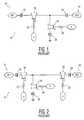
- FIG. 1shows a series-shunt arm of a prior art switch.
- the armincludes a series path between two signal ports, as provided by a series FET 16 .
- a shunt FET 24provides a shunt path to enhance the isolation between the two signal ports when the arm is in an OFF state.
- the channel of the series FET 16is biased such that V gs falls below V p , creating a high impedance between the two signal ports dominated by the junction capacitances of the series FET.
- the V gs of the shunt FET 24is biased by V′ to be above
- the series FET 16alone provides a great deal of isolation between the two signal ports, the low impedance path to ground, as provided by the shunt FET, enhances the isolation. Since for the OFF state the bias voltage V for the series FET is below (V RF1 ⁇ V p ) and the bias voltage V′ for the shunt FET is above
- FIG. 2discloses a prior art switch similar to FIG. 1, but having a multistage configuration.
- the switch of FIG. 2also requires opposite logic states for the proper biasing of the series FETs and shunt FET.
- Typical control logic for such prior art switchesincludes various active and passive components.
- a feedforward capacitor with a low impedancecan be used to improve the harmonic rejection of an FET. By improving the harmonic rejection, signal distortions and noise interferences can be reduced or eliminated, and the performance of the FET structures can be improved greatly.
- Feedforward capacitorsare often employed in designs seeking high isolation and power handling.
- the feedforward capacitormay be coupled across the gate of an FET and a signal port.
- the present inventiontherefore provides a switch having at least two signal ports in series with at least one series FET connected therebetween, and a shunt path having a FET, whereby a control voltage is applied to a gate on the series FET and to a drain on the shunt FET.
- the switchincludes a control signal input, an FET having a current path connected in series between the first port and the second port, the series FET having a control electrode or gate coupled to the control signal input, and a shunt path provided by an FET, the shunt FET having a drain coupled to the control signal input and to the gate of the series FET, whereby a single control signal is applied to both the series FET and the shunt FET, via the control signal input, in order to turn the series FET on and simultaneously turn the shunt FET off and, conversely, in order to turn the series FET off and simultaneously turn the shunt FET on.
- the present inventionalso provides a method for switching, including the step of using a common logic signal to control both a switch and a shunt in a series arrangement.
- the present inventionfurther provides a method of controlling the coupling of a first port to a second port via a series shunt FET switch.
- the methodincludes the steps of isolating the first port from the second port, using a single control signal, by turning off the series FET.
- the series FETis turned off by biasing the gate-source voltage below the pinchoff voltage.
- the shunt FETis turned on by biasing the gate-source voltage above the pinchoff voltage.
- the methodalso includes the step of coupling the first port to the second port, using a single control signal, by turning on the series FET.
- the series FETis turned on by biasing the gate-source voltage above the pinchoff voltage.
- the shunt FETis turned off by biasing the gate-source voltage below the pinchoff voltage.
- FIG. 1is a schematic diagram of a prior art series/shunt arm of a switch
- FIG. 2is a schematic diagram of a prior art switch similar to FIG. 1, but in a multi-gate configuration
- FIG. 3is a schematic diagram of a switch in accordance with the present invention.
- FIG. 4is a schematic diagram of a switch in accordance with a further embodiment of the present invention.
- FIG. 5is a schematic diagram of a switch in accordance with yet a further embodiment of the present invention.
- FIG. 6is a schematic diagram of a switch in accordance with the present invention, in a multi-gate configuration, and used feedforward capacitors;
- FIG. 7is a schematic representation of the circuit shown in FIG. 6, showing gate-source and gate-drain junction capacitances of the series FETs in an OFF state.
- FIG. 1discloses a prior art switch 10 having a first signal port 12 coupled to a second signal port 14 via a series FET 16 .
- the series FET 16includes a drain, source and gate.
- the source of FET 16is coupled to the first port 12 via series capacitor 18 and the drain is coupled to the second port 14 via series capacitor 20 .
- the gateis coupled to a control voltage V via a resistor 22 .
- a shunt FET 24includes a source, drain and gate.
- the source of the shunt FET 24is coupled to a ground reference via a capacitor 26 .
- the drain of the shunt FET 24is coupled to the drain of the series FET 16 .
- FIG. 2is similar to the prior art switch 10 of FIG. 1, but in a multi-gate configuration.
- the switch 10 ′ of FIG. 2further includes a second series FET 30 .
- the second series FET 30includes a drain, source and gate. The gate is coupled to a control voltage V via a resistor 32 .
- FIG. 3illustrates a first embodiment of the invention.
- a switch indicated generally at 40includes a switching transistor 42 having a current path and a control electrode.
- transistor 42is a series FET 42 having a source, drain and gate.
- the source of the series FET 42is coupled to the first signal port 12 through signal path 51 and capacitor 13 .
- the drain of the series FET 42is coupled to the second signal port 14 through blocking capacitor 21 .
- the gate or control electrode of the series FET 42is coupled to control signal bias voltage V via a resistor 44 .
- a shunt transistor 46provides a switchable path coupling the gate or control electrode of switching transistor 42 to a ground reference.
- Shunt FET 46includes a drain, source and gate.
- the drain of the shunt FET 46is coupled to the gate of the series FET 42 .
- the source of the shunt FET 46is coupled to a ground reference via a capacitor 48 .
- the gate of the shunt FET 46is coupled to a ground reference via a resistor 50 .
- the shunt FET 46will turn on as long as V is biased above
- below Vhie.g., Vhi
- the series FET 42will turn on.
- the shunt FET 46will turn off as long as V is biased>
- the FETsare turned on and off through the gate-source voltage bias.
- the schematic shown in FIG. 3allows the control signal V to be applied to the gate on the series FET 42 and conversely to the drain on the shunt FET 46 .
- This techniqueallows for the same control signal to have the opposite effect on each respective device and so for a common logic signal to control both a series and shunt device on a common path.
- the series FET 42When the series FET 42 is off, the gate-source and gate-drain junction capacitances dominate the impedance of the device (high impedance state). Simultaneously, FET 46 is on when FET 42 is off, enhancing the isolation to port 14 by shunting the signal from port 12 to ground. When the series FET 42 is on, the low impedance of its channel dominates and provides a path for the signal to flow from the first signal port 12 to the second signal port 14 . At the same time, the shunt FET 46 is off, which further reduces the loss through the shunt path to ground.
- FIG. 4is a schematic diagram of the switch of FIG. 3, in a modified embodiment.
- the switch of FIG. 4further includes a resistor 52 which is coupled across the source and drain of the shunt FET 46 . This sharpens the timing of the switching of shunt FET 46 between an ON and OFF state.
- FIG. 5is a schematic of a switch similar to FIG. 1, but in a further modified embodiment.
- FIG. 5further includes a resistor 54 which is coupled across the source of the shunt FET 46 and the bias or control voltage V.
- any desired plurality of series pathsmay be implemented using similar techniques as those shown in the embodiment of FIG. 3.
- Embodimentsmay be scaled for multi-gate devices or multiple series FETs. Additionally, it should be noted, redistributing the RF voltage across the junction capacitors in a manner similar to what would be present in a design with feedforward capacitors, the shunt FET application in FIG. 3 can also aid in power handling.
- feedforward capacitors 60are connected to the shunt paths of the series/shunt switch arms.
- FIG. 6also shows the employment of an additional series FET 59 to permit a relatively low control voltage without increasing die or periphery size.
- a further advantage of the present inventionis that the use of a shunt FET connected to the gate provides a “short” across a junction capacitance to ground similar to that which is present with feedforward capacitors.
- FIG. 7is a diagram of the circuit shown in FIG. 6 showing the gate-source and gate-drain junction capacitances in the series FETs' OFF state being represented by capacitors.
- This modeldemonstrates that the blocking capacitor (Cff/Csh) 60 performs a number of tasks more or less simultaneously: a DC block for the shunt arm; a low impedance for high isolation; and the equivalent feedforward capacitance for power handling.
- one or more of these tasksmay not be desired and the embodiment may be modified as appropriate and/or necessary.
- the illustrated embodiments of the present inventionuse metal semiconductor field-effect transistors (MESFETs) as the solid state switching devices employed.
- MESFETsmetal semiconductor field-effect transistors
- the present inventionhas application to circuits using junction field-effect transistors (JFETs), metal-oxide field-effect transistors (MOSFETs), high electron mobility transistors (HEMTs), pseudomorphic high electron mobility field-effect transistors (PHEMTs), and other variants of field-effect transistor (FETs) devices.
- JFETsjunction field-effect transistors
- MOSFETsmetal-oxide field-effect transistors
- HEMTshigh electron mobility transistors
- PHEMTspseudomorphic high electron mobility field-effect transistors
- FETsfield-effect transistor
Landscapes
- Electronic Switches (AREA)
Abstract
Description
- This application claims priority to Provisional Application Serial No. 60/434,365 filed Dec. 17, 2002, the contents of which are fully incorporated by reference herein.[0001]
- The present invention relates in general to switch devices, and more particularly to a series/shunt FET switch between two signal ports.[0002]
- Conventional switch devices operate to control the path on which a signal travels. One example of a transistor-based switch is comprised of a plurality of field effect transistors (FETs). FET switches are generally known to be used in connection with high frequency signal transmission, for example, radio frequency (RF).[0003]
- In general, an n-channel FET switch is in an ON state (very low impedance) allowing any signal to pass from the source to the drain of the FET until a control voltage applied to the gate of the FET falls below a predetermined amount. When the control voltage is removed, the FET switches to an OFF state (very high impedance) and prevents any signal passing from the source to the drain of the FET. The control voltage is selected such that the magnitude of the gate-to-source voltage of the FET, V[0004]gs, rises above the magnitude of a threshold “pinchoff” voltage Vp. The advantage of a FET switch is that the control voltage applied to the gate of the FET draws very little current, consuming little power in performing the switching function. Switches may be combined with shunts, for example, in applications where a switch is used between two or more signal ports so as to increase isolation between the ports.
- For example, FIG. 1 shows a series-shunt arm of a prior art switch. The arm includes a series path between two signal ports, as provided by a series FET[0005]16. A
shunt FET 24 provides a shunt path to enhance the isolation between the two signal ports when the arm is in an OFF state. In the OFF state, the channel of the series FET16 is biased such that Vgsfalls below Vp, creating a high impedance between the two signal ports dominated by the junction capacitances of the series FET. However, the Vgsof theshunt FET 24 is biased by V′ to be above |Vp|, creating a low impedance path to ground. Although the series FET16 alone provides a great deal of isolation between the two signal ports, the low impedance path to ground, as provided by the shunt FET, enhances the isolation. Since for the OFF state the bias voltage V for the series FET is below (VRF1−Vp) and the bias voltage V′ for the shunt FET is above |Vp|, then the equivalent logic states that control these arms are inverted from one another. Therefore, opposite logic states must be available to switch the path between the two signal ports from least attenuation to maximum isolation. - In the ON state for the series-shunt arm, the channel of the series FET[0006]16 is biased above Vpcreating a low impedance between the two signal ports. However, the channel of the shunt FET24 is biased below Vpcreating a high impedance path to ground. With such equivalent logic states or biases applied to the switch, minimum attenuation is achieved by decreasing the loss between the signal ports and minimizing the coupling of the signal to ground through the shunt path. Similar to the OFF state, the series and shunt FETs require opposite logic states.
- FIG. 2 discloses a prior art switch similar to FIG. 1, but having a multistage configuration. The switch of FIG. 2 also requires opposite logic states for the proper biasing of the series FETs and shunt FET.[0007]
- Typical control logic for such prior art switches includes various active and passive components.[0008]
- A feedforward capacitor with a low impedance can be used to improve the harmonic rejection of an FET. By improving the harmonic rejection, signal distortions and noise interferences can be reduced or eliminated, and the performance of the FET structures can be improved greatly. Feedforward capacitors are often employed in designs seeking high isolation and power handling. The feedforward capacitor may be coupled across the gate of an FET and a signal port.[0009]
- It is a feature of the present invention to provide a series/shunt switch which does not require inverted control logic to control the ON/OFF state of the switch.[0010]
- It is a feature of the present invention to provide a series/shunt switch, and method of control, which is controlled by a common logic signal.[0011]
- It is a feature of the present invention to eliminate redundant control logic components.[0012]
- It is a feature of the present invention to provide a series/shunt switch device which integrates a feedforward capacitor in order to benefit from the associated advantages.[0013]
- It is a feature of the present invention to provide a series/shunt switch having a reduced die size.[0014]
- It is a feature of the present invention to provide a series/shunt switch which is less costly to manufacture.[0015]
- The present invention therefore provides a switch having at least two signal ports in series with at least one series FET connected therebetween, and a shunt path having a FET, whereby a control voltage is applied to a gate on the series FET and to a drain on the shunt FET.[0016]
- In one embodiment, the switch includes a control signal input, an FET having a current path connected in series between the first port and the second port, the series FET having a control electrode or gate coupled to the control signal input, and a shunt path provided by an FET, the shunt FET having a drain coupled to the control signal input and to the gate of the series FET, whereby a single control signal is applied to both the series FET and the shunt FET, via the control signal input, in order to turn the series FET on and simultaneously turn the shunt FET off and, conversely, in order to turn the series FET off and simultaneously turn the shunt FET on.[0017]
- The present invention also provides a method for switching, including the step of using a common logic signal to control both a switch and a shunt in a series arrangement.[0018]
- The present invention further provides a method of controlling the coupling of a first port to a second port via a series shunt FET switch. The method includes the steps of isolating the first port from the second port, using a single control signal, by turning off the series FET. The series FET is turned off by biasing the gate-source voltage below the pinchoff voltage. During the same period, the shunt FET is turned on by biasing the gate-source voltage above the pinchoff voltage. The method also includes the step of coupling the first port to the second port, using a single control signal, by turning on the series FET. The series FET is turned on by biasing the gate-source voltage above the pinchoff voltage. During the same period, the shunt FET is turned off by biasing the gate-source voltage below the pinchoff voltage.[0019]
- These and other aspects of the invention and their advantages will be discerned in the following detailed description when read in conjunction with the drawings, in which like parts are denoted by like characters and in which:[0020]
- FIG. 1 is a schematic diagram of a prior art series/shunt arm of a switch;[0021]
- FIG. 2 is a schematic diagram of a prior art switch similar to FIG. 1, but in a multi-gate configuration;[0022]
- FIG. 3 is a schematic diagram of a switch in accordance with the present invention;[0023]
- FIG. 4 is a schematic diagram of a switch in accordance with a further embodiment of the present invention;[0024]
- FIG. 5 is a schematic diagram of a switch in accordance with yet a further embodiment of the present invention;[0025]
- FIG. 6 is a schematic diagram of a switch in accordance with the present invention, in a multi-gate configuration, and used feedforward capacitors; and[0026]
- FIG. 7 is a schematic representation of the circuit shown in FIG. 6, showing gate-source and gate-drain junction capacitances of the series FETs in an OFF state.[0027]
- FIG. 1 discloses a[0028]
prior art switch 10 having afirst signal port 12 coupled to asecond signal port 14 via a series FET16. The series FET16 includes a drain, source and gate. The source of FET16 is coupled to thefirst port 12 viaseries capacitor 18 and the drain is coupled to thesecond port 14 viaseries capacitor 20. The gate is coupled to a control voltage V via aresistor 22. A shunt FET24 includes a source, drain and gate. The source of theshunt FET 24 is coupled to a ground reference via acapacitor 26. The drain of theshunt FET 24 is coupled to the drain of theseries FET 16. The gate of theshunt FET 24 is coupled to a control voltage V′ via aresistor 28. FIG. 2 is similar to theprior art switch 10 of FIG. 1, but in a multi-gate configuration. In particular, theswitch 10′ of FIG. 2 further includes asecond series FET 30. Thesecond series FET 30 includes a drain, source and gate. The gate is coupled to a control voltage V via aresistor 32. - FIG. 3 illustrates a first embodiment of the invention. A switch indicated generally at[0029]40 includes a switching
transistor 42 having a current path and a control electrode. In the illustrated embodiment,transistor 42 is aseries FET 42 having a source, drain and gate. The source of theseries FET 42 is coupled to thefirst signal port 12 throughsignal path 51 andcapacitor 13. The drain of theseries FET 42 is coupled to thesecond signal port 14 through blockingcapacitor 21. The gate or control electrode of theseries FET 42 is coupled to control signal bias voltage V via aresistor 44. Ashunt transistor 46 provides a switchable path coupling the gate or control electrode of switchingtransistor 42 to a ground reference.Shunt FET 46 includes a drain, source and gate. The drain of theshunt FET 46 is coupled to the gate of theseries FET 42. The source of theshunt FET 46 is coupled to a ground reference via acapacitor 48. The gate of theshunt FET 46 is coupled to a ground reference via aresistor 50. During transmission of a signal fromport 12 toport 14, or vice versa, a voltage Vhi relative to ground is placed onsignal path 51. When any bias applied to V is less than Vpbelow Vhi (e.g., 0V, when Vhi>Vp), then theseries FET 42 will turn off. Simultaneously, theshunt FET 46 will turn on as long as V is biased above |Vp|(Vgs=0−V>Vp=>shunt device on). When any bias applied to V is greater than |Vp| below Vhi (e.g., Vhi), then theseries FET 42 will turn on. Simultaneously, theshunt FET 46 will turn off as long as V is biased>|Vp| (e.g. Vgs=−V<Vp=>shunt device off). - Thus the FETs are turned on and off through the gate-source voltage bias. The schematic shown in FIG. 3 allows the control signal V to be applied to the gate on the[0030]
series FET 42 and conversely to the drain on theshunt FET 46. This technique allows for the same control signal to have the opposite effect on each respective device and so for a common logic signal to control both a series and shunt device on a common path. - When the[0031]
series FET 42 is off, the gate-source and gate-drain junction capacitances dominate the impedance of the device (high impedance state). Simultaneously,FET 46 is on whenFET 42 is off, enhancing the isolation to port14 by shunting the signal fromport 12 to ground. When theseries FET 42 is on, the low impedance of its channel dominates and provides a path for the signal to flow from thefirst signal port 12 to thesecond signal port 14. At the same time, theshunt FET 46 is off, which further reduces the loss through the shunt path to ground. - FIG. 4 is a schematic diagram of the switch of FIG. 3, in a modified embodiment. The switch of FIG. 4 further includes a[0032]
resistor 52 which is coupled across the source and drain of theshunt FET 46. This sharpens the timing of the switching ofshunt FET 46 between an ON and OFF state. - FIG. 5 is a schematic of a switch similar to FIG. 1, but in a further modified embodiment. FIG. 5 further includes a[0033]
resistor 54 which is coupled across the source of theshunt FET 46 and the bias or control voltage V. - In other embodiments, any desired plurality of series paths may be implemented using similar techniques as those shown in the embodiment of FIG. 3. Embodiments may be scaled for multi-gate devices or multiple series FETs. Additionally, it should be noted, redistributing the RF voltage across the junction capacitors in a manner similar to what would be present in a design with feedforward capacitors, the shunt FET application in FIG. 3 can also aid in power handling.[0034]
- Additionally, embodiments using feedforward capacitors for power handling may also use similar techniques to those shown in FIG. 3. For example, as shown by FIG. 6,[0035]
feedforward capacitors 60 are connected to the shunt paths of the series/shunt switch arms. FIG. 6 also shows the employment of anadditional series FET 59 to permit a relatively low control voltage without increasing die or periphery size. - A further advantage of the present invention is that the use of a shunt FET connected to the gate provides a “short” across a junction capacitance to ground similar to that which is present with feedforward capacitors. FIG. 7 is a diagram of the circuit shown in FIG. 6 showing the gate-source and gate-drain junction capacitances in the series FETs' OFF state being represented by capacitors. This model demonstrates that the blocking capacitor (Cff/Csh)[0036]60 performs a number of tasks more or less simultaneously: a DC block for the shunt arm; a low impedance for high isolation; and the equivalent feedforward capacitance for power handling. Of course, in other embodiments, one or more of these tasks may not be desired and the embodiment may be modified as appropriate and/or necessary.
- Further, in embodiments where high isolation and power handling are desired, minimal die space is used.[0037]
- The illustrated embodiments of the present invention use metal semiconductor field-effect transistors (MESFETs) as the solid state switching devices employed. However the present invention has application to circuits using junction field-effect transistors (JFETs), metal-oxide field-effect transistors (MOSFETs), high electron mobility transistors (HEMTs), pseudomorphic high electron mobility field-effect transistors (PHEMTs), and other variants of field-effect transistor (FETs) devices.[0038]
- Although this invention has been illustrated by reference to specific embodiments, it will be apparent to those skilled in the art that various changes and modifications may be made which clearly fall within the scope of the invention. The invention is intended to be protected broadly within the spirit and scope of the appended claims.[0039]
Claims (23)
Priority Applications (6)
| Application Number | Priority Date | Filing Date | Title |
|---|---|---|---|
| US10/648,022US7250804B2 (en) | 2002-12-17 | 2003-08-26 | Series/shunt switch and method of control |
| JP2005509960AJP2006511179A (en) | 2002-12-17 | 2003-12-16 | Switch and switch control method |
| EP03799919AEP1573918A1 (en) | 2002-12-17 | 2003-12-16 | Series/shunt switch and method of operation |
| AU2003299635AAU2003299635A1 (en) | 2002-12-17 | 2003-12-16 | Series/shunt switch and method of operation |
| PCT/US2003/039955WO2004059842A1 (en) | 2002-12-17 | 2003-12-16 | Series/shunt switch and method of operation |
| US11/821,204US7786787B2 (en) | 2002-12-17 | 2007-06-22 | Series/shunt switch and method of control |
Applications Claiming Priority (2)
| Application Number | Priority Date | Filing Date | Title |
|---|---|---|---|
| US43436502P | 2002-12-17 | 2002-12-17 | |
| US10/648,022US7250804B2 (en) | 2002-12-17 | 2003-08-26 | Series/shunt switch and method of control |
Related Child Applications (1)
| Application Number | Title | Priority Date | Filing Date |
|---|---|---|---|
| US11/821,204ContinuationUS7786787B2 (en) | 2002-12-17 | 2007-06-22 | Series/shunt switch and method of control |
Publications (2)
| Publication Number | Publication Date |
|---|---|
| US20040113746A1true US20040113746A1 (en) | 2004-06-17 |
| US7250804B2 US7250804B2 (en) | 2007-07-31 |
Family
ID=32511748
Family Applications (2)
| Application Number | Title | Priority Date | Filing Date |
|---|---|---|---|
| US10/648,022Expired - LifetimeUS7250804B2 (en) | 2002-12-17 | 2003-08-26 | Series/shunt switch and method of control |
| US11/821,204Expired - LifetimeUS7786787B2 (en) | 2002-12-17 | 2007-06-22 | Series/shunt switch and method of control |
Family Applications After (1)
| Application Number | Title | Priority Date | Filing Date |
|---|---|---|---|
| US11/821,204Expired - LifetimeUS7786787B2 (en) | 2002-12-17 | 2007-06-22 | Series/shunt switch and method of control |
Country Status (5)
| Country | Link |
|---|---|
| US (2) | US7250804B2 (en) |
| EP (1) | EP1573918A1 (en) |
| JP (1) | JP2006511179A (en) |
| AU (1) | AU2003299635A1 (en) |
| WO (1) | WO2004059842A1 (en) |
Cited By (27)
| Publication number | Priority date | Publication date | Assignee | Title |
|---|---|---|---|---|
| US20050212674A1 (en)* | 2004-03-29 | 2005-09-29 | Impinj, Inc., A Delaware Corporation | RFID tag uncoupling one of its antenna ports and methods |
| US20060049917A1 (en)* | 2004-03-31 | 2006-03-09 | Impinj, Inc. | RFID tags combining signals received from multiple RF ports |
| US20060055620A1 (en)* | 2004-03-29 | 2006-03-16 | Impinj, Inc. | Circuits for RFID tags with multiple non-independently driven RF ports |
| USD586336S1 (en) | 2004-12-30 | 2009-02-10 | Impinj, Inc. | Radio frequency identification tag antenna assembly |
| US20090121975A1 (en)* | 2007-11-13 | 2009-05-14 | Samsung Electronics Co., Ltd. | Display apparatus and control method thereof |
| US20090230978A1 (en)* | 2006-05-10 | 2009-09-17 | Advantest Corporation | Switch circuit, filter circuit and test apparatus |
| US20110133841A1 (en)* | 2008-11-19 | 2011-06-09 | Supertex, Inc. | Low Noise Binary-Coded Gain Amplifier And Method For Time-Gain Compensation In Medical Ultrasound Imaging |
| US20120176178A1 (en)* | 2011-01-06 | 2012-07-12 | Tse-Lung Yang | Switch circuit capable of preventing voltage spike, and control method and layout structure thereof |
| WO2014066421A1 (en)* | 2012-10-22 | 2014-05-01 | Qualcomm Incorporated | Amplifiers with noise splitting |
| US8774334B2 (en) | 2011-11-09 | 2014-07-08 | Qualcomm Incorporated | Dynamic receiver switching |
| US8995591B2 (en) | 2013-03-14 | 2015-03-31 | Qualcomm, Incorporated | Reusing a single-chip carrier aggregation receiver to support non-cellular diversity |
| US9026070B2 (en) | 2003-12-18 | 2015-05-05 | Qualcomm Incorporated | Low-power wireless diversity receiver with multiple receive paths |
| US9118439B2 (en) | 2012-04-06 | 2015-08-25 | Qualcomm Incorporated | Receiver for imbalanced carriers |
| US9154356B2 (en) | 2012-05-25 | 2015-10-06 | Qualcomm Incorporated | Low noise amplifiers for carrier aggregation |
| US9154179B2 (en) | 2011-06-29 | 2015-10-06 | Qualcomm Incorporated | Receiver with bypass mode for improved sensitivity |
| US9172402B2 (en) | 2012-03-02 | 2015-10-27 | Qualcomm Incorporated | Multiple-input and multiple-output carrier aggregation receiver reuse architecture |
| US9172404B1 (en) | 2005-02-07 | 2015-10-27 | Rf Micro Devices, Inc. | Switch architecture for TDMA and FDD multiplexing |
| US9178669B2 (en) | 2011-05-17 | 2015-11-03 | Qualcomm Incorporated | Non-adjacent carrier aggregation architecture |
| US9252827B2 (en) | 2011-06-27 | 2016-02-02 | Qualcomm Incorporated | Signal splitting carrier aggregation receiver architecture |
| US9300420B2 (en) | 2012-09-11 | 2016-03-29 | Qualcomm Incorporated | Carrier aggregation receiver architecture |
| US9362958B2 (en) | 2012-03-02 | 2016-06-07 | Qualcomm Incorporated | Single chip signal splitting carrier aggregation receiver architecture |
| US9450665B2 (en) | 2005-10-19 | 2016-09-20 | Qualcomm Incorporated | Diversity receiver for wireless communication |
| US9867194B2 (en) | 2012-06-12 | 2018-01-09 | Qualcomm Incorporated | Dynamic UE scheduling with shared antenna and carrier aggregation |
| US10177722B2 (en) | 2016-01-12 | 2019-01-08 | Qualcomm Incorporated | Carrier aggregation low-noise amplifier with tunable integrated power splitter |
| US10693231B2 (en) | 2017-09-11 | 2020-06-23 | Qualcomm Incorporated | Transmit/receive switching circuit |
| CN114374379A (en)* | 2021-12-29 | 2022-04-19 | 西安博瑞集信电子科技有限公司 | Single-chip positive-voltage controlled low-control-voltage high-power-capacity single-pole double-throw switch |
| US12081243B2 (en) | 2011-08-16 | 2024-09-03 | Qualcomm Incorporated | Low noise amplifiers with combined outputs |
Families Citing this family (21)
| Publication number | Priority date | Publication date | Assignee | Title |
|---|---|---|---|---|
| US20050184407A1 (en)* | 2004-02-20 | 2005-08-25 | Takahiro Korenari | Transistor circuit, thin film transistor circuit and display device |
| US7408396B2 (en)* | 2006-05-18 | 2008-08-05 | Continental Teves, Inc. | High voltage protection circuit |
| US20090108911A1 (en)* | 2007-10-30 | 2009-04-30 | Rohm Co., Ltd. | Analog switch |
| US8299835B2 (en)* | 2008-02-01 | 2012-10-30 | Sensor Electronic Technology, Inc. | Radio-frequency switch circuit with separately controlled shunt switching device |
| US7646231B2 (en)* | 2008-02-11 | 2010-01-12 | Avago Technologies Wireless Ip (Singapore) Pte. Ltd. | System and method for controlling attenuator |
| US8008988B1 (en) | 2008-02-20 | 2011-08-30 | Triquint Semiconductor, Inc. | Radio frequency switch with improved intermodulation distortion through use of feed forward capacitor |
| US7679417B2 (en)* | 2008-07-10 | 2010-03-16 | Avago Technologies Wireless Ip (Singapore) Pte. Ltd. | Attenuator with bias control circuit |
| US8498576B2 (en)* | 2010-04-08 | 2013-07-30 | Georgia Tech Research Corporation | Inverse-mode bipolar transistor radio-frequency switches and methods of using same |
| US10056895B2 (en) | 2010-04-27 | 2018-08-21 | Qorvo Us, Inc. | High power FET switch |
| US9209784B2 (en) | 2010-04-27 | 2015-12-08 | Rf Micro Devices, Inc. | Switchable capacitive elements for programmable capacitor arrays |
| US8330519B2 (en) | 2010-07-09 | 2012-12-11 | Sige Semiconductor Inc. | System and method of transistor switch biasing in a high power semiconductor switch |
| US20140374766A1 (en)* | 2013-06-20 | 2014-12-25 | Texas Instruments Incorporated | Bi-directional gallium nitride switch with self-managed substrate bias |
| US9628195B2 (en)* | 2014-10-22 | 2017-04-18 | Source Photonics (Chengdu) Co., Ltd. | Transimpedance amplifier (TIA) having an enlarged dynamic range and optical devices using the same |
| CN106026976B (en)* | 2015-03-26 | 2020-09-18 | 松下电器产业株式会社 | Switch control circuit |
| WO2017083596A1 (en)* | 2015-11-13 | 2017-05-18 | Skyworks Solutions, Inc. | Integrated switch-filter network |
| GB2564482B (en)* | 2017-07-14 | 2021-02-10 | Cambridge Entpr Ltd | A power semiconductor device with a double gate structure |
| US11336279B2 (en) | 2017-07-14 | 2022-05-17 | Cambridge Enterprise Limited | Power semiconductor device with a series connection of two devices |
| US11257811B2 (en) | 2017-07-14 | 2022-02-22 | Cambridge Enterprise Limited | Power semiconductor device with an auxiliary gate structure |
| US11955478B2 (en)* | 2019-05-07 | 2024-04-09 | Cambridge Gan Devices Limited | Power semiconductor device with an auxiliary gate structure |
| US12382651B2 (en)* | 2019-05-07 | 2025-08-05 | Cambridge Gan Devices Limited | Power semiconductor device with an auxiliary gate structure |
| US11677392B2 (en) | 2021-04-16 | 2023-06-13 | Analog Devices International Unlimited Company | Bias networks for DC or extended low frequency capable fast stacked switches |
Citations (18)
| Publication number | Priority date | Publication date | Assignee | Title |
|---|---|---|---|---|
| US233206A (en)* | 1880-10-12 | Carding-machine | ||
| US3731116A (en)* | 1972-03-02 | 1973-05-01 | Us Navy | High frequency field effect transistor switch |
| US3872325A (en)* | 1973-10-17 | 1975-03-18 | Rca Corp | R-F switching circuit |
| US4158149A (en)* | 1977-05-16 | 1979-06-12 | Hitachi Denshi Kabushiki Kaisha | Electronic switching circuit using junction type field-effect transistor |
| US4678929A (en)* | 1985-09-30 | 1987-07-07 | Rca Corporation | Radio frequency switch |
| US4742249A (en)* | 1986-11-25 | 1988-05-03 | Rca Licensing Corporation | RF switch with diode network and control latch sharing common element |
| US5107152A (en)* | 1989-09-08 | 1992-04-21 | Mia-Com, Inc. | Control component for a three-electrode device |
| US5301081A (en)* | 1992-07-16 | 1994-04-05 | Pacific Monolithics | Input protection circuit |
| US5705940A (en)* | 1990-07-16 | 1998-01-06 | Raytheon Company | Logic family for digitally controlled analog monolithic microwave integrated circuits |
| US5717356A (en)* | 1995-01-23 | 1998-02-10 | Sony Corporation | Low insertion loss switch |
| US5767721A (en)* | 1996-06-06 | 1998-06-16 | Itt Industries, Inc. | Switch circuit for FET devices having negative threshold voltages which utilize a positive voltage only |
| US5818099A (en)* | 1996-10-03 | 1998-10-06 | International Business Machines Corporation | MOS high frequency switch circuit using a variable well bias |
| US5818283A (en)* | 1995-07-13 | 1998-10-06 | Japan Radio Co., Ltd. | High power FET switch |
| US6229370B1 (en)* | 1998-04-24 | 2001-05-08 | Matsushita Electric Industrial Co., Ltd. | Amplifier |
| US6426525B1 (en)* | 2001-04-18 | 2002-07-30 | Tyco Electronics Corporation | FET structures having symmetric and/or distributed feedforward capacitor connections |
| US6496072B2 (en)* | 1999-12-29 | 2002-12-17 | Samsung Electronics, Co., Ltd. | Amplifying apparatus for a mobile station receiver and method for controlling the same |
| US6518823B1 (en)* | 1999-08-31 | 2003-02-11 | Sony Computer Entertainment Inc. | One-time programmable logic device |
| US6720850B2 (en)* | 2001-04-10 | 2004-04-13 | Murata Manufacturing Co., Ltd. | Variable attenuator |
Family Cites Families (6)
| Publication number | Priority date | Publication date | Assignee | Title |
|---|---|---|---|---|
| JPS5980974A (en)* | 1982-11-01 | 1984-05-10 | Nippon Telegr & Teleph Corp <Ntt> | high frequency switch |
| JPS6097720A (en)* | 1983-11-02 | 1985-05-31 | Nec Corp | High frequency switch circuit |
| JP3284015B2 (en)* | 1995-02-02 | 2002-05-20 | 東芝マイクロエレクトロニクス株式会社 | Semiconductor integrated circuit |
| US6504449B2 (en) | 2000-02-07 | 2003-01-07 | Anritsu Company | Phase compensated switched attenuation pad |
| WO2001067602A2 (en)* | 2000-03-03 | 2001-09-13 | Alpha Industries, Inc. | Electronic switch |
| JP2002246942A (en)* | 2001-02-19 | 2002-08-30 | Sony Corp | Switching device and portable communication terminal device |
- 2003
- 2003-08-26USUS10/648,022patent/US7250804B2/ennot_activeExpired - Lifetime
- 2003-12-16EPEP03799919Apatent/EP1573918A1/ennot_activeWithdrawn
- 2003-12-16WOPCT/US2003/039955patent/WO2004059842A1/enactiveApplication Filing
- 2003-12-16JPJP2005509960Apatent/JP2006511179A/ennot_activeCeased
- 2003-12-16AUAU2003299635Apatent/AU2003299635A1/ennot_activeAbandoned
- 2007
- 2007-06-22USUS11/821,204patent/US7786787B2/ennot_activeExpired - Lifetime
Patent Citations (18)
| Publication number | Priority date | Publication date | Assignee | Title |
|---|---|---|---|---|
| US233206A (en)* | 1880-10-12 | Carding-machine | ||
| US3731116A (en)* | 1972-03-02 | 1973-05-01 | Us Navy | High frequency field effect transistor switch |
| US3872325A (en)* | 1973-10-17 | 1975-03-18 | Rca Corp | R-F switching circuit |
| US4158149A (en)* | 1977-05-16 | 1979-06-12 | Hitachi Denshi Kabushiki Kaisha | Electronic switching circuit using junction type field-effect transistor |
| US4678929A (en)* | 1985-09-30 | 1987-07-07 | Rca Corporation | Radio frequency switch |
| US4742249A (en)* | 1986-11-25 | 1988-05-03 | Rca Licensing Corporation | RF switch with diode network and control latch sharing common element |
| US5107152A (en)* | 1989-09-08 | 1992-04-21 | Mia-Com, Inc. | Control component for a three-electrode device |
| US5705940A (en)* | 1990-07-16 | 1998-01-06 | Raytheon Company | Logic family for digitally controlled analog monolithic microwave integrated circuits |
| US5301081A (en)* | 1992-07-16 | 1994-04-05 | Pacific Monolithics | Input protection circuit |
| US5717356A (en)* | 1995-01-23 | 1998-02-10 | Sony Corporation | Low insertion loss switch |
| US5818283A (en)* | 1995-07-13 | 1998-10-06 | Japan Radio Co., Ltd. | High power FET switch |
| US5767721A (en)* | 1996-06-06 | 1998-06-16 | Itt Industries, Inc. | Switch circuit for FET devices having negative threshold voltages which utilize a positive voltage only |
| US5818099A (en)* | 1996-10-03 | 1998-10-06 | International Business Machines Corporation | MOS high frequency switch circuit using a variable well bias |
| US6229370B1 (en)* | 1998-04-24 | 2001-05-08 | Matsushita Electric Industrial Co., Ltd. | Amplifier |
| US6518823B1 (en)* | 1999-08-31 | 2003-02-11 | Sony Computer Entertainment Inc. | One-time programmable logic device |
| US6496072B2 (en)* | 1999-12-29 | 2002-12-17 | Samsung Electronics, Co., Ltd. | Amplifying apparatus for a mobile station receiver and method for controlling the same |
| US6720850B2 (en)* | 2001-04-10 | 2004-04-13 | Murata Manufacturing Co., Ltd. | Variable attenuator |
| US6426525B1 (en)* | 2001-04-18 | 2002-07-30 | Tyco Electronics Corporation | FET structures having symmetric and/or distributed feedforward capacitor connections |
Cited By (38)
| Publication number | Priority date | Publication date | Assignee | Title |
|---|---|---|---|---|
| US9026070B2 (en) | 2003-12-18 | 2015-05-05 | Qualcomm Incorporated | Low-power wireless diversity receiver with multiple receive paths |
| US20050212674A1 (en)* | 2004-03-29 | 2005-09-29 | Impinj, Inc., A Delaware Corporation | RFID tag uncoupling one of its antenna ports and methods |
| US7528728B2 (en)* | 2004-03-29 | 2009-05-05 | Impinj Inc. | Circuits for RFID tags with multiple non-independently driven RF ports |
| US20060055620A1 (en)* | 2004-03-29 | 2006-03-16 | Impinj, Inc. | Circuits for RFID tags with multiple non-independently driven RF ports |
| US7667589B2 (en) | 2004-03-29 | 2010-02-23 | Impinj, Inc. | RFID tag uncoupling one of its antenna ports and methods |
| US7423539B2 (en) | 2004-03-31 | 2008-09-09 | Impinj, Inc. | RFID tags combining signals received from multiple RF ports |
| US7525438B2 (en) | 2004-03-31 | 2009-04-28 | Impinj, Inc. | RFID tags combining signals received from multiple RF ports |
| US20060049917A1 (en)* | 2004-03-31 | 2006-03-09 | Impinj, Inc. | RFID tags combining signals received from multiple RF ports |
| USD586336S1 (en) | 2004-12-30 | 2009-02-10 | Impinj, Inc. | Radio frequency identification tag antenna assembly |
| US9172404B1 (en) | 2005-02-07 | 2015-10-27 | Rf Micro Devices, Inc. | Switch architecture for TDMA and FDD multiplexing |
| US9450665B2 (en) | 2005-10-19 | 2016-09-20 | Qualcomm Incorporated | Diversity receiver for wireless communication |
| US20090230978A1 (en)* | 2006-05-10 | 2009-09-17 | Advantest Corporation | Switch circuit, filter circuit and test apparatus |
| US8232808B2 (en) | 2006-05-10 | 2012-07-31 | Advantest Corporation | Switch circuit, filter circuit and test apparatus |
| US20090121975A1 (en)* | 2007-11-13 | 2009-05-14 | Samsung Electronics Co., Ltd. | Display apparatus and control method thereof |
| US20110133841A1 (en)* | 2008-11-19 | 2011-06-09 | Supertex, Inc. | Low Noise Binary-Coded Gain Amplifier And Method For Time-Gain Compensation In Medical Ultrasound Imaging |
| US20120176178A1 (en)* | 2011-01-06 | 2012-07-12 | Tse-Lung Yang | Switch circuit capable of preventing voltage spike, and control method and layout structure thereof |
| US9178669B2 (en) | 2011-05-17 | 2015-11-03 | Qualcomm Incorporated | Non-adjacent carrier aggregation architecture |
| US9252827B2 (en) | 2011-06-27 | 2016-02-02 | Qualcomm Incorporated | Signal splitting carrier aggregation receiver architecture |
| US9154179B2 (en) | 2011-06-29 | 2015-10-06 | Qualcomm Incorporated | Receiver with bypass mode for improved sensitivity |
| US12081243B2 (en) | 2011-08-16 | 2024-09-03 | Qualcomm Incorporated | Low noise amplifiers with combined outputs |
| US8774334B2 (en) | 2011-11-09 | 2014-07-08 | Qualcomm Incorporated | Dynamic receiver switching |
| US9362958B2 (en) | 2012-03-02 | 2016-06-07 | Qualcomm Incorporated | Single chip signal splitting carrier aggregation receiver architecture |
| US9172402B2 (en) | 2012-03-02 | 2015-10-27 | Qualcomm Incorporated | Multiple-input and multiple-output carrier aggregation receiver reuse architecture |
| US9118439B2 (en) | 2012-04-06 | 2015-08-25 | Qualcomm Incorporated | Receiver for imbalanced carriers |
| US9154356B2 (en) | 2012-05-25 | 2015-10-06 | Qualcomm Incorporated | Low noise amplifiers for carrier aggregation |
| US9166852B2 (en) | 2012-05-25 | 2015-10-20 | Qualcomm Incorporated | Low noise amplifiers with transformer-based signal splitting for carrier aggregation |
| US9160598B2 (en) | 2012-05-25 | 2015-10-13 | Qualcomm Incorporated | Low noise amplifiers with cascode divert switch for carrier aggregation |
| US9154357B2 (en) | 2012-05-25 | 2015-10-06 | Qualcomm Incorporated | Multiple-input multiple-output (MIMO) low noise amplifiers for carrier aggregation |
| US9867194B2 (en) | 2012-06-12 | 2018-01-09 | Qualcomm Incorporated | Dynamic UE scheduling with shared antenna and carrier aggregation |
| US9300420B2 (en) | 2012-09-11 | 2016-03-29 | Qualcomm Incorporated | Carrier aggregation receiver architecture |
| US9837968B2 (en) | 2012-10-22 | 2017-12-05 | Qualcomm Incorporated | Amplifier circuits |
| US9543903B2 (en) | 2012-10-22 | 2017-01-10 | Qualcomm Incorporated | Amplifiers with noise splitting |
| WO2014066421A1 (en)* | 2012-10-22 | 2014-05-01 | Qualcomm Incorporated | Amplifiers with noise splitting |
| US8995591B2 (en) | 2013-03-14 | 2015-03-31 | Qualcomm, Incorporated | Reusing a single-chip carrier aggregation receiver to support non-cellular diversity |
| US10177722B2 (en) | 2016-01-12 | 2019-01-08 | Qualcomm Incorporated | Carrier aggregation low-noise amplifier with tunable integrated power splitter |
| US10693231B2 (en) | 2017-09-11 | 2020-06-23 | Qualcomm Incorporated | Transmit/receive switching circuit |
| US10910714B2 (en) | 2017-09-11 | 2021-02-02 | Qualcomm Incorporated | Configurable power combiner and splitter |
| CN114374379A (en)* | 2021-12-29 | 2022-04-19 | 西安博瑞集信电子科技有限公司 | Single-chip positive-voltage controlled low-control-voltage high-power-capacity single-pole double-throw switch |
Also Published As
| Publication number | Publication date |
|---|---|
| US7786787B2 (en) | 2010-08-31 |
| AU2003299635A1 (en) | 2004-07-22 |
| US20070247211A1 (en) | 2007-10-25 |
| US7250804B2 (en) | 2007-07-31 |
| EP1573918A1 (en) | 2005-09-14 |
| JP2006511179A (en) | 2006-03-30 |
| WO2004059842A1 (en) | 2004-07-15 |
Similar Documents
| Publication | Publication Date | Title |
|---|---|---|
| US7250804B2 (en) | Series/shunt switch and method of control | |
| JP3736356B2 (en) | High frequency switch circuit | |
| US6693498B1 (en) | SPDT switch and communication unit using the same | |
| JP3790227B2 (en) | High frequency switch circuit | |
| US7492209B2 (en) | High-frequency switching device with reduced harmonics | |
| US20070290744A1 (en) | Radio frequency switching circuit, radio frequency switching device, and transmitter module device | |
| US6154085A (en) | Constant gate drive MOS analog switch | |
| US20060252394A1 (en) | Switching circuit | |
| JPH0927736A (en) | FET switch | |
| JPH09181588A (en) | Semiconductor switch | |
| WO2004023670A1 (en) | A 2v spdt switch for high power rf wireless applications | |
| WO2022187003A1 (en) | Dual voltage switched branch lna architecture | |
| CN100405739C (en) | Series / shunt switch and operation method | |
| US7852172B2 (en) | High-power switch | |
| US6873200B2 (en) | Electronic switch | |
| KR20020067531A (en) | Bootstrapped dual-gate class e amplifier circuit | |
| US6900711B2 (en) | Switching system | |
| JP7357562B2 (en) | high frequency switch circuit | |
| JP2005072993A (en) | Fet switch circuit | |
| JP3539106B2 (en) | High frequency semiconductor switch circuit and control method using the same | |
| JP2007258766A (en) | Semiconductor switch circuit | |
| JPH0738404A (en) | Output switching amplifier | |
| JP7425623B2 (en) | high frequency switch circuit | |
| JP2001160724A (en) | Amplifier with switch | |
| JP3630545B2 (en) | RF signal switch circuit |
Legal Events
| Date | Code | Title | Description |
|---|---|---|---|
| AS | Assignment | Owner name:M/A COM, INC., MASSACHUSETTS Free format text:ASSIGNMENT OF ASSIGNORS INTEREST;ASSIGNOR:BRINDLE, CHRISTOPHER N.;REEL/FRAME:014450/0625 Effective date:20030825 | |
| STCF | Information on status: patent grant | Free format text:PATENTED CASE | |
| AS | Assignment | Owner name:COBHAM DEFENSE ELECTRONIC SYSTEMS CORPORATION, MAS Free format text:ASSIGNMENT OF ASSIGNORS INTEREST;ASSIGNORS:M/A COM, INC.;RAYCHEM INTERNATIONAL;TYCO ELECTRONICS CORPORATION;AND OTHERS;REEL/FRAME:022266/0400;SIGNING DATES FROM 20080108 TO 20090113 Owner name:COBHAM DEFENSE ELECTRONIC SYSTEMS CORPORATION,MASS Free format text:ASSIGNMENT OF ASSIGNORS INTEREST;ASSIGNORS:M/A COM, INC.;RAYCHEM INTERNATIONAL;TYCO ELECTRONICS CORPORATION;AND OTHERS;SIGNING DATES FROM 20080108 TO 20090113;REEL/FRAME:022266/0400 Owner name:COBHAM DEFENSE ELECTRONIC SYSTEMS CORPORATION, MAS Free format text:ASSIGNMENT OF ASSIGNORS INTEREST;ASSIGNORS:M/A COM, INC.;RAYCHEM INTERNATIONAL;TYCO ELECTRONICS CORPORATION;AND OTHERS;SIGNING DATES FROM 20080108 TO 20090113;REEL/FRAME:022266/0400 | |
| AS | Assignment | Owner name:COBHAM DEFENSE ELECTRONIC SYSTEMS CORPORATION, MAS Free format text:SECURITY AGREEMENT;ASSIGNOR:KIWI STONE ACQUISITION CORP.;REEL/FRAME:022482/0016 Effective date:20090330 Owner name:COBHAM DEFENSE ELECTRONIC SYSTEMS CORPORATION,MASS Free format text:SECURITY AGREEMENT;ASSIGNOR:KIWI STONE ACQUISITION CORP.;REEL/FRAME:022482/0016 Effective date:20090330 | |
| AS | Assignment | Owner name:KIWI STONE ACQUISITION CORPORATION, CALIFORNIA Free format text:ASSIGNMENT OF ASSIGNORS INTEREST;ASSIGNOR:COBHAM DEFENSE ELECTRONIC SYSTEMS CORPORATION;REEL/FRAME:022714/0890 Effective date:20090521 Owner name:KIWI STONE ACQUISITION CORPORATION,CALIFORNIA Free format text:ASSIGNMENT OF ASSIGNORS INTEREST;ASSIGNOR:COBHAM DEFENSE ELECTRONIC SYSTEMS CORPORATION;REEL/FRAME:022714/0890 Effective date:20090521 | |
| AS | Assignment | Owner name:M/A-COM TECHNOLOGY SOLUTIONS HOLDINGS, INC., MASSA Free format text:CHANGE OF NAME;ASSIGNOR:KIWI STONE ACQUISITION CORP.;REEL/FRAME:023476/0069 Effective date:20090526 Owner name:M/A-COM TECHNOLOGY SOLUTIONS HOLDINGS, INC.,MASSAC Free format text:CHANGE OF NAME;ASSIGNOR:KIWI STONE ACQUISITION CORP.;REEL/FRAME:023476/0069 Effective date:20090526 | |
| AS | Assignment | Owner name:RBS BUSINESS CAPITAL, A DIVISION OF RBS ASSET FINA Free format text:SECURITY AGREEMENT;ASSIGNORS:MIMIX BROADBAND, INC.;M/A-COM TECHNOLOGY SOLUTIONS HOLDINGS, INC.;REEL/FRAME:025444/0920 Effective date:20101203 | |
| AS | Assignment | Owner name:M/A-COM TECHNOLOGY SOLUTIONS HOLDINGS, INC., MASSA Free format text:RELEASE BY SECURED PARTY;ASSIGNOR:COBHAM DEFENSE ELECTRONIC SYSTEMS CORPORATION;REEL/FRAME:025445/0947 Effective date:20101203 | |
| FPAY | Fee payment | Year of fee payment:4 | |
| AS | Assignment | Owner name:JPMORGAN CHASE BANK, N.A., AS ADMINISTRATIVE AGENT Free format text:SECURITY AGREEMENT;ASSIGNOR:M/A-COM TECHNOLOGY SOLUTIONS HOLDINGS, INC.;REEL/FRAME:027015/0444 Effective date:20110930 | |
| AS | Assignment | Owner name:M/A-COM TECHNOLOGY SOLUTIONS HOLDINGS, INC., MASSA Free format text:RELEASE OF SECURITY INTEREST RECORDED AT REEL/FRAME 25444/920;ASSIGNOR:RBS BUSINESS CAPITAL, A DIVISION OF RBS ASSET FINANCE, INC., AS ADMINISTRATIVE AGENT;REEL/FRAME:027028/0021 Effective date:20110930 Owner name:MIMIX BROADBAND, INC., MASSACHUSETTS Free format text:RELEASE OF SECURITY INTEREST RECORDED AT REEL/FRAME 25444/920;ASSIGNOR:RBS BUSINESS CAPITAL, A DIVISION OF RBS ASSET FINANCE, INC., AS ADMINISTRATIVE AGENT;REEL/FRAME:027028/0021 Effective date:20110930 | |
| AS | Assignment | Owner name:JPMORGAN CHASE BANK, N.A., AS ADMINISTRATIVE AGENT Free format text:SECURITY AGREEMENT;ASSIGNOR:M/A-COM TECHNOLOGY SOLUTIONS HOLDINGS, INC.;REEL/FRAME:031314/0183 Effective date:20130926 | |
| FEPP | Fee payment procedure | Free format text:PAYOR NUMBER ASSIGNED (ORIGINAL EVENT CODE: ASPN); ENTITY STATUS OF PATENT OWNER: LARGE ENTITY | |
| AS | Assignment | Owner name:M/A-COM TECHNOLOGY SOLUTIONS HOLDINGS, INC., MASSA Free format text:RELEASE BY SECURED PARTY;ASSIGNOR:JPMORGAN CHASE BANK, N.A.;REEL/FRAME:032857/0032 Effective date:20140508 | |
| AS | Assignment | Owner name:GOLDMAN SACHS BANK USA, NEW YORK Free format text:SECURITY INTEREST;ASSIGNORS:M/A-COM TECHNOLOGY SOLUTIONS HOLDINGS, INC.;MINDSPEED TECHNOLOGIES, INC.;BROOKTREE CORPORATION;REEL/FRAME:032859/0374 Effective date:20140508 | |
| FPAY | Fee payment | Year of fee payment:8 | |
| AS | Assignment | Owner name:MACOM TECHNOLOGY SOLUTIONS HOLDINGS, INC., MASSACH Free format text:CHANGE OF NAME;ASSIGNOR:M/A-COM TECHNOLOGY SOLUTIONS HOLDINGS, INC.;REEL/FRAME:039139/0826 Effective date:20160601 | |
| FEPP | Fee payment procedure | Free format text:MAINTENANCE FEE REMINDER MAILED (ORIGINAL EVENT CODE: REM.); ENTITY STATUS OF PATENT OWNER: LARGE ENTITY | |
| FEPP | Fee payment procedure | Free format text:11.5 YR SURCHARGE- LATE PMT W/IN 6 MO, LARGE ENTITY (ORIGINAL EVENT CODE: M1556); ENTITY STATUS OF PATENT OWNER: LARGE ENTITY | |
| MAFP | Maintenance fee payment | Free format text:PAYMENT OF MAINTENANCE FEE, 12TH YEAR, LARGE ENTITY (ORIGINAL EVENT CODE: M1553); ENTITY STATUS OF PATENT OWNER: LARGE ENTITY Year of fee payment:12 |