US20040113645A1 - Wafer level burn-in and electrical test system and method - Google Patents
Wafer level burn-in and electrical test system and methodDownload PDFInfo
- Publication number
- US20040113645A1 US20040113645A1US10/718,825US71882503AUS2004113645A1US 20040113645 A1US20040113645 A1US 20040113645A1US 71882503 AUS71882503 AUS 71882503AUS 2004113645 A1US2004113645 A1US 2004113645A1
- Authority
- US
- United States
- Prior art keywords
- test
- circuit board
- printed circuit
- electronics
- zone
- Prior art date
- Legal status (The legal status is an assumption and is not a legal conclusion. Google has not performed a legal analysis and makes no representation as to the accuracy of the status listed.)
- Granted
Links
- 238000012360testing methodMethods0.000titleclaimsabstractdescription171
- 238000000034methodMethods0.000titleclaimsdescription10
- 239000000523sampleSubstances0.000claimsabstractdescription67
- 239000004065semiconductorSubstances0.000claimsabstractdescription25
- 230000007704transitionEffects0.000claimsabstractdescription12
- 239000004606Fillers/ExtendersSubstances0.000claimsdescription21
- 238000005259measurementMethods0.000claimsdescription8
- XUIMIQQOPSSXEZ-UHFFFAOYSA-NSiliconChemical compound[Si]XUIMIQQOPSSXEZ-UHFFFAOYSA-N0.000claims1
- 230000005669field effectEffects0.000claims1
- 229910044991metal oxideInorganic materials0.000claims1
- 150000004706metal oxidesChemical class0.000claims1
- 229910052710siliconInorganic materials0.000claims1
- 239000010703siliconSubstances0.000claims1
- 150000003071polychlorinated biphenylsChemical class0.000description42
- RIMXLXBUOQMDHV-UHFFFAOYSA-N1,2-dichloro-4-(2-chlorophenyl)benzeneChemical compoundC1=C(Cl)C(Cl)=CC=C1C1=CC=CC=C1ClRIMXLXBUOQMDHV-UHFFFAOYSA-N0.000description20
- MTCPZNVSDFCBBE-UHFFFAOYSA-N1,3,5-trichloro-2-(2,6-dichlorophenyl)benzeneChemical compoundClC1=CC(Cl)=CC(Cl)=C1C1=C(Cl)C=CC=C1ClMTCPZNVSDFCBBE-UHFFFAOYSA-N0.000description12
- 239000004020conductorSubstances0.000description11
- BQENMISTWGTJIJ-UHFFFAOYSA-N2,3,3',4,5-pentachlorobiphenylChemical compoundClC1=CC=CC(C=2C(=C(Cl)C(Cl)=C(Cl)C=2)Cl)=C1BQENMISTWGTJIJ-UHFFFAOYSA-N0.000description10
- BWWVXHRLMPBDCK-UHFFFAOYSA-N1,2,4-trichloro-5-(2,6-dichlorophenyl)benzeneChemical compoundC1=C(Cl)C(Cl)=CC(Cl)=C1C1=C(Cl)C=CC=C1ClBWWVXHRLMPBDCK-UHFFFAOYSA-N0.000description8
- 238000010586diagramMethods0.000description7
- 239000003292glueSubstances0.000description5
- MPCDNZSLJWJDNW-UHFFFAOYSA-N1,2,3-trichloro-4-(3,5-dichlorophenyl)benzeneChemical compoundClC1=CC(Cl)=CC(C=2C(=C(Cl)C(Cl)=CC=2)Cl)=C1MPCDNZSLJWJDNW-UHFFFAOYSA-N0.000description2
- ARXHIJMGSIYYRZ-UHFFFAOYSA-N1,2,4-trichloro-3-(3,4-dichlorophenyl)benzeneChemical compoundC1=C(Cl)C(Cl)=CC=C1C1=C(Cl)C=CC(Cl)=C1ClARXHIJMGSIYYRZ-UHFFFAOYSA-N0.000description2
- 230000002950deficientEffects0.000description2
- 238000011156evaluationMethods0.000description2
- 238000002955isolationMethods0.000description2
- 239000002184metalSubstances0.000description2
- 229910052751metalInorganic materials0.000description2
- 238000000926separation methodMethods0.000description2
- BSFZSQRJGZHMMV-UHFFFAOYSA-N1,2,3-trichloro-5-phenylbenzeneChemical compoundClC1=C(Cl)C(Cl)=CC(C=2C=CC=CC=2)=C1BSFZSQRJGZHMMV-UHFFFAOYSA-N0.000description1
- VGVIKVCCUATMNG-UHFFFAOYSA-N1,2,4-trichloro-5-phenylbenzeneChemical compoundC1=C(Cl)C(Cl)=CC(Cl)=C1C1=CC=CC=C1VGVIKVCCUATMNG-UHFFFAOYSA-N0.000description1
- SXZSFWHOSHAKMN-UHFFFAOYSA-N2,3,4,4',5-PentachlorobiphenylChemical compoundC1=CC(Cl)=CC=C1C1=CC(Cl)=C(Cl)C(Cl)=C1ClSXZSFWHOSHAKMN-UHFFFAOYSA-N0.000description1
- RYGMFSIKBFXOCR-UHFFFAOYSA-NCopperChemical compound[Cu]RYGMFSIKBFXOCR-UHFFFAOYSA-N0.000description1
- 241000218691CupressaceaeSpecies0.000description1
- 241000408659DarpaSpecies0.000description1
- 230000008859changeEffects0.000description1
- 238000009833condensationMethods0.000description1
- 230000005494condensationEffects0.000description1
- 238000010276constructionMethods0.000description1
- 229910052802copperInorganic materials0.000description1
- 239000010949copperSubstances0.000description1
- 230000001351cycling effectEffects0.000description1
- 230000006378damageEffects0.000description1
- 230000006870functionEffects0.000description1
- 238000004519manufacturing processMethods0.000description1
- 239000000463materialSubstances0.000description1
- 230000013011matingEffects0.000description1
- 238000004806packaging method and processMethods0.000description1
- 230000008569processEffects0.000description1
- 238000012545processingMethods0.000description1
- 230000000452restraining effectEffects0.000description1
- 238000012163sequencing techniqueMethods0.000description1
- 238000010008shearingMethods0.000description1
- 230000003685thermal hair damageEffects0.000description1
- 238000012546transferMethods0.000description1
Images


Classifications
- G—PHYSICS
- G01—MEASURING; TESTING
- G01R—MEASURING ELECTRIC VARIABLES; MEASURING MAGNETIC VARIABLES
- G01R31/00—Arrangements for testing electric properties; Arrangements for locating electric faults; Arrangements for electrical testing characterised by what is being tested not provided for elsewhere
- G01R31/28—Testing of electronic circuits, e.g. by signal tracer
- G01R31/2851—Testing of integrated circuits [IC]
- G01R31/2855—Environmental, reliability or burn-in testing
- G01R31/286—External aspects, e.g. related to chambers, contacting devices or handlers
- G01R31/2868—Complete testing stations; systems; procedures; software aspects
- G01R31/287—Procedures; Software aspects
- G—PHYSICS
- G01—MEASURING; TESTING
- G01R—MEASURING ELECTRIC VARIABLES; MEASURING MAGNETIC VARIABLES
- G01R31/00—Arrangements for testing electric properties; Arrangements for locating electric faults; Arrangements for electrical testing characterised by what is being tested not provided for elsewhere
- G01R31/28—Testing of electronic circuits, e.g. by signal tracer
- G01R31/2851—Testing of integrated circuits [IC]
- G01R31/2855—Environmental, reliability or burn-in testing
- G01R31/286—External aspects, e.g. related to chambers, contacting devices or handlers
- G01R31/2868—Complete testing stations; systems; procedures; software aspects
- G—PHYSICS
- G01—MEASURING; TESTING
- G01R—MEASURING ELECTRIC VARIABLES; MEASURING MAGNETIC VARIABLES
- G01R31/00—Arrangements for testing electric properties; Arrangements for locating electric faults; Arrangements for electrical testing characterised by what is being tested not provided for elsewhere
- G01R31/28—Testing of electronic circuits, e.g. by signal tracer
- G01R31/2851—Testing of integrated circuits [IC]
- G01R31/2886—Features relating to contacting the IC under test, e.g. probe heads; chucks
- G—PHYSICS
- G01—MEASURING; TESTING
- G01R—MEASURING ELECTRIC VARIABLES; MEASURING MAGNETIC VARIABLES
- G01R31/00—Arrangements for testing electric properties; Arrangements for locating electric faults; Arrangements for electrical testing characterised by what is being tested not provided for elsewhere
- G01R31/28—Testing of electronic circuits, e.g. by signal tracer
- G01R31/282—Testing of electronic circuits specially adapted for particular applications not provided for elsewhere
- G01R31/2831—Testing of materials or semi-finished products, e.g. semiconductor wafers or substrates
- G—PHYSICS
- G01—MEASURING; TESTING
- G01R—MEASURING ELECTRIC VARIABLES; MEASURING MAGNETIC VARIABLES
- G01R31/00—Arrangements for testing electric properties; Arrangements for locating electric faults; Arrangements for electrical testing characterised by what is being tested not provided for elsewhere
- G01R31/28—Testing of electronic circuits, e.g. by signal tracer
- G01R31/2851—Testing of integrated circuits [IC]
- G01R31/2855—Environmental, reliability or burn-in testing
- G01R31/286—External aspects, e.g. related to chambers, contacting devices or handlers
- G01R31/2863—Contacting devices, e.g. sockets, burn-in boards or mounting fixtures
- H—ELECTRICITY
- H05—ELECTRIC TECHNIQUES NOT OTHERWISE PROVIDED FOR
- H05K—PRINTED CIRCUITS; CASINGS OR CONSTRUCTIONAL DETAILS OF ELECTRIC APPARATUS; MANUFACTURE OF ASSEMBLAGES OF ELECTRICAL COMPONENTS
- H05K3/00—Apparatus or processes for manufacturing printed circuits
- H05K3/46—Manufacturing multilayer circuits
- H05K3/4688—Composite multilayer circuits, i.e. comprising insulating layers having different properties
- H05K3/4691—Rigid-flexible multilayer circuits comprising rigid and flexible layers, e.g. having in the bending regions only flexible layers
Definitions
- the present inventionrelates generally to a system and method for evaluation of integrated circuits and other semiconductor devices. More particularly, it relates a system incorporating hardware and suitable interconnections which allow efficient burn-in testing of a multiplicity of semiconductor devices while still incorporated in a semiconductor wafer.
- This inventionis related to the inventions in commonly owned U.S. Pat. No. 5,429,510, issued to Barraclough et al. on Jul. 5, 1995, entitled “High-Density Interconnect Technique,” and commonly owned U.S. Pat. No. 5,682,472, issued to Brehm et al. on Oct. 28, 1997 and entitled “Method and System for Testing Memory Programming Devices,” the disclosures of which are hereby incorporated by reference herein.
- This inventionis further related to the invention in a concurrently filed, copending, commonly owned application filed in the names of Frank 0 . Uher. Mark C. Carbone, John W. Andberg and Donald P. Richmond II, entitled “Wafer Level Burm-In and Test Cartridge” (Attorney Docket No. AEHR-006/00US), the disclosure of which is also incorporated by reference herein.
- burn-inrelates to operation of an integrated circuit at a predetermined temperature or temperature profile, typically an elevated temperature in an oven, a reduced temperature in an environmentally controlled enclosure, or a combination of an elevated temperature followed by a reduced temperature.
- Certain operating electrical bias levels and/or signalsare supplied to the semiconductor devices while they are at the elevated temperature.
- the use of the elevated temperature or the combination of an elevated temperature followed by a reduced temperatureaccelerates stress to which the devices are subjected during burn-in, so that marginal devices that would otherwise fail shortly after being placed in service fail during burn-in and are eliminated before shipping.
- electrical testa more complete set of operating electrical bias levels and signals are supplied to the device to provide a thorough evaluation of its functions.
- Wafer-level burn-in systemshave attracted interest because they allow defective integrated circuits to be identified by the burn-in process before additional expense is incurred in their handling and packaging. Similarly, it is desirable to carry out electrical test of the integrated circuits while they are still in wafer form. Electrical test involves applying a suite of electrical signal inputs to each integrated circuit to make sure that it performs properly for its intended use.
- the present inventionis directed to solving those problems.
- aspects of the present inventionmay, however, be employed in a system that carries out wafer-level burn-in or wafer-level electrical test alone.
- a burn-in test systemincludes a device under test zone configured to receive a plurality of cartridges each containing a semiconductor wafer including a plurality of integrated circuits.
- Each of the plurality of cartridgesincludes a rigid probe signal printed circuit board and a probe power printed circuit board substantially parallel to and closely spaced from the rigid probe printed circuit board.
- Test electronicsare positioned adjacent to the device under test zone.
- Power electronicsare positioned adjacent to said device under test zone.
- a first interconnection systemconnects the test electronics to the rigid probe signal printed circuit board.
- a second interconnection systemconnects the power electronics to the probe power printed circuit board.
- the first and second interconnection systemsare arranged in a stacked relationship.
- the probe power printed circuit boardhas at least a bendable section permitting a portion of the probe power printed circuit board to be spaced a greater distance away from the rigid probe signal printed circuit board proximate to the second interconnection system.
- a test systemincludes a device under test zone configured to receive a plurality of cartridges each containing a semiconductor wafer including a plurality of integrated circuits.
- Each of the plurality of cartridgesincludes a rigid probe signal printed circuit board and a probe power printed circuit board substantially parallel to and closely spaced from the rigid probe printed circuit board.
- Test electronicsare positioned adjacent to said device under test zone.
- Power electronicsare positioned adjacent to the device under test zone.
- a first interconnection systemconnects the test electronics to the rigid probe signal printed circuit board.
- a second interconnection systemconnects the power electronics to the probe power printed circuit board.
- the first and second interconnection systemsare arranged in a stacked relationship.
- the probe power printed circuit boardhas at least a bendable section permitting a portion of the probe power printed circuit board to be spaced a greater distance away from the rigid probe signal printed circuit board proximate to the second interconnection system.
- a burn-in systemhas a temperature controlled zone configured to receive a plurality of cartridges each containing a semiconductor wafer including a plurality of integrated circuits.
- Test electronicsare positioned in a cool zone.
- Power electronicsare positioned in the cool zone.
- a transition zoneseparates the temperature controlled zone and the cool zone.
- a test systemin a fourth aspect of the invention, includes a device under test zone configured to receive a plurality of cartridges each containing a semiconductor wafer including a plurality of integrated circuits.
- Test electronics on a first circuit boardare positioned adjacent to the device under test zone.
- Power electronics on a second circuit boardare positioned adjacent to said device under test zone.
- Each of the plurality of cartridgesare connected to the test electronics by a first connection between one of the plurality of cartridges and the first circuit board and to the power electronics by a second connection between the one of said plurality of cartridges and the second circuit board separate from the first connection.
- a test systemin a fifth aspect of the invention, includes a first plurality of test channels each adapted to receive a second plurality of integrated circuits under test.
- a second plurality of power modulesare each connected to one of the integrated circuits under test in each test channel.
- a controlleris connected and configured for successive selection of one of the first plurality of test channels.
- a method for burn-in testing integrated circuits in wafer formincludes providing a temperature controlled zone configured to receive a plurality of cartridges each containing a semiconductor wafer including a plurality of integrated circuits.
- the integrated circuitsare tested with test electronics positioned in a cool zone.
- Poweris provided to the integrated circuits with power electronics positioned in the cool zone.
- the test and power electronicsare separated from the temperature controlled zone with a transition zone between the temperature controlled zone and the cool zone.
- a method for testing integrated circuits in wafer formincludes connecting a first plurality of integrated circuits in a second plurality of test channels.
- a first plurality of power modulesis connected to one of the integrated circuits under test in each test channel.
- One of the second plurality of test channelsis selectively selected.
- the first plurality of the integrated circuits in the selected test channelis tested. The selective selection and testing steps are repeated until all of the integrated circuits have been tested.
- FIG. 1is a block diagram and schematic representation of an embodiment of a burn-in and electrical test system in accordance with the invention.
- FIG. 2is a block diagram and schematic representation of part of the system shown in FIG. 1.
- FIG. 3is another more detailed block diagram and schematic representation of the part of the system shown in FIG. 2.
- FIG. 4is a partially exploded block diagram of the part of the system shown in FIG. 3.
- FIG. 4Ais a cross section view of an interconnection system used in the part of the system portion shown in FIG. 2.
- FIG. 5is a block diagram of another part of the system shown in FIGS. 1 - 4 .
- FIGS. 6 and 7are circuit diagrams of a portion of the system part of FIG. 5.
- FIGS. 8 and 9are pinout connection diagrams of integrated circuits under burn-in and test using the invention.
- FIGS. 10 and 11are somewhat schematic representations of interconnections used in the system portion shown in FIGS. 2 - 4 .
- FIG. 12is a cross section view of a portion of the interconnections shown in FIG. 10.
- FIG. 13is a plan view of a portion of the interconnections shown in FIG. 10.
- FIG. 14is a cross section view of a portion of the interconnections shown in FIG. 11.
- FIG. 15is a cross section view of one of the interconnections in the system portion shown in FIGS. 2 - 4 .
- FIGS. 16A. 16 B and 16 Care perspective, top and side views of a part of the interconnection shown in FIG. 15.
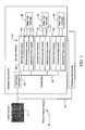
- FIG. 1there is shown a burn-in and electrical test system 20 in accordance with the invention.
- a local controller 21is connected to a plurality of electrical test zones # 1 through #n via an internal Ethernet network 101 .
- Electrical test zone # 1shows the details of each electrical test zone.
- Each of the electrical test zoneshas a single test pattern generator 103 connected by a parallel bus 105 to a plurality of test slots 107 comprising a test slot interface 119 .
- Each test slot 107comprises optional fault analysis 109 , a driver comparator board 111 and a wafer/die power system 113 .
- Two separate connections for each wafer test cartridge 26 for test electronics and for power distributionare represented at 115 and 117 .
- the optional fault analysis 109 and driver comparator board 111comprise the test electronics and are connected to the wafer test cartridge 26 by connection 115 .
- the wafer/die power system 113is connected to the wafer test cartridge 26 by connection 117 .
- FIG. 2shows a portion of the system 20 of FIG. 1.
- a plurality of wafer cartridges 26are connected to test electronics 28 and power electronics 30 .
- the test electronics 28comprises a single pattern generator printed circuit board (PCB) 29 and separate signal driver and fault analysis PCBs 33 for each wafer cartridge 26 .
- Each of the wafer cartridges 26contains a semiconductor wafer incorporating a plurality of integrated circuits. All of the signal driver and fault analysis PCBs 33 are connected to the pattern generator PCB by parallel bus 105 . Further details of the cartridges 26 are contained in a concurrently filed, co-owned pending application entitled “Wafer Level Burn-In and Test Cartridge and Alignment Method,” filed in the names of Frank O. Uher, Mark C. Carbone, John W.
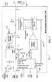
- FIGS. 3 and 4show further details of the wafer cartridge 26 .
- test electronics 28 and power electronics 30and how they are interconnected.
- the test electronics 28consists of a pattern generator PCB 29 and a signal driver and fault analysis PCB 33 connected together by the parallel bus 105 .
- the fault analysis PCB 33is connected to a rigid signal probe PCB 104 in cartridge 26 through a driver extender PCB 102 to provide a straight through signal path.
- the probe PCB 104is rigid in order to allow close control of impedance between each signal line and a backplane, to be discussed more fully below in connection with FIGS. 10, 12 and 13 , thus providing impedance controlled interconnections between a semiconductor wafer under test and the test electronics 28 .
- the portion of the system 20 shown in FIGS. 3 and 4is divided into a temperature controlled zone 22 , a cool or ambient temperature zone 24 and a transition zone 25 .
- the temperature controlled zoneis either heated to an elevated temperature, such as 150° C., or chilled, such as to a temperature of 0° C. during the burn-in or test operation.
- the wafer cartridge 26extends from the temperature controlled zone 22 into the transition zone 25 .
- a thermal dam 156is positioned around the wafer cartridge 26 at the interface between the temperature controlled zone and the transition zone to minimize heat transfer between the zones around the cartridge 26 .
- the transition zone 25is provided in order to prevent heat or cold leakage from the controlled temperature zone into the signal driver and fault analysis PCB 33 . Such heat or cold leakage would change the temperature of the PCB 33 over time, thus causing a performance chance, resulting in a variation of test conditions over time. Additionally, cold leakage into the PCB 33 would result in condensation or thermal damage to the PCB 33 .
- the driver extender PCB 102serves to space the signal driver and fault analysis PCB 33 from the temperature controlled zone 22 and the transition zone 25 for further heat and cold isolation. Additionally, the driver extender PCB 102 permits impedance matching of the signal probe PCB and the signal driver and fault analysis PCB 33 .
- the signal probe PCB 104has an impedance of about 50 ohm
- the signal driver and fault analysis PCB 33has an impedance of about 28 ohm.
- the driver extender PCBhas a varying impedance along its length, from about 28 ohm on the signal driver and fault analysis PCB 33 end to about 50 ohm on the signal probe PCB 104 end. This impedance matching permits higher quality signals to be transmitted between the signal driver and fault analysis PCB 33 and the signal probe PCB 104 .
- the power distribution system 30is connected to a probe power PCB 106 in the cartridge 26 .
- the probe PCB 106has a flexible portion 107 order to allow it to be positioned closely adjacent to and parallel with the rigid probe PCB 104 along most of its extent in the cartridge 26 , yet extend a substantial distance away from the probe PCB 106 at its interconnection with the power distribution system 30 .
- the cartridge 26is connected to the test electronics 28 and the power distribution system 30 through a mini-backplane PCB 108 .
- High pin density connectors 109are used to connect the cartridge 26 to the driver extender PCB 102 and to the power distribution system 30 .
- the connectors 109include a total of 4200 pin connections, compared with a total of 680 pin connections in the system described in the above-referenced Brehm et al. patent.
- the connectorshave insulated pins and the signal pins are set in an electromagnetic interference (EMI) shield housing.
- EMIelectromagnetic interference
- Suitable high pin density connectors 109 of this typeare commercially available from AMP Incorporated, Harrisburg, Pa. and will not be further described herein.
- the power distribution system 30includes a die power main PCB 110 and a set 118 of 32-channel die power dual-in-line modules (DIMs) mounted on the die power main PCB 110 .
- the driver extender board 102is connected to a main signal driver PCB 33 by an interconnection system 31 .
- a set 120 of signal driver DIMs and a fault analysis PCB 114are mounted on the main signal driver PCB 33 .
- FIG. 4Ashows details of the interconnection 31 .
- This interconnection systemis the subject of the above-referenced Barraclough et al. patent.
- the system 31employs contact fingers 32 on both surfaces 34 and 36 of PCB 102 and PCB 33 .
- Each of the PCBs 102 and 33has a card-edge connector 44 and 46 .
- the contact fingers 32 and the card-edge connectors 44 and 46 of each PCBmate inversely with each other on adjacent PCBs, i.e., the card-edge connector 44 of the PCB 102 mates with contact fingers 32 of the PCB 33 , and the card-edge connector 46 of the PCB 33 mates with the contact fingers of the PCB 102 .
- the PCB 102has two sets 70 and 72 of interconnections connected to metal contacts 74 of the card-edge connector 44 and two sets of 76 and 78 of interconnections connected to contact fingers 32 of the PCB 33 .
- PCB 33has two sets 80 and 82 of interconnections connected to contact fingers 32 of the PCB 33 and two sets 84 and 86 of interconnections connected to metal contacts 88 of the card-edge connector 46 .
- this interconnection system 31there is twice the density of interconnects per inch using the same card-edge connector compared with a typical prior art interconnection system, for example. 40 interconnects per inch of card edge between two PCBs, compared with 20 interconnects per inch in the prior art example.
- the interconnection system 31is self-aligning.
- the card-edge connectors 44 and 46are each set back from the contact fingers of their respective PCBs 38 and 40 .
- PCBs 38 and 40of the same thickness and using connectors 44 and 46 with identical geometry that are mounted directly on the PCBs for both PCBs that are connected together, all dimensional relationships are maintained when the assembly is inverted for the second connection.
- Connector support bars 90are provided, fixedly attached (such as bolted) on each PCB 38 and 40 behind the connectors 44 and 46 to provide sufficient structural rigidity and support for plugging and unplugging the connectors 44 and 46 .
- FIG. 5shows the parallel test processing capability and segmented power distribution of the system 20 .
- Each power module 280is connected to 32 devices under test 200 comprising 32 channels. While carrying out the testing, only one of the 32 channels is made active at a time using the chip select lines 282 . This means that only one device under test 200 is powered by each power module 280 at a time, thus resulting in far less need for capacitance per power module 280 .
- poweris supplied to all of the devices 200 under test in their inactive state, but only one device per power module is powered to its active state at a time. The active state uses power at a much higher level and makes much more electrical noise on the power lines.
- each power moduleis provided to satisfy current demand when cycling from low to high power demand at high frequencies.
- FIG. 6shows a circuit schematic of the power module 280 .
- the power module 280has a microcontrol element 252 connected at 254 to control turning on and turning off an MOS FET power switch 256 .
- the microcontrol element 252can be implemented as an microcontroller, a field programmable gate array (FPGA) or a Cypress progammable logic device (CPLD).
- a Vdd input 253is connected to input 255 of the power switch 256 .
- Output 258 of the power switch 256is connected to the device under test (DUT) 200 .
- DUTdevice under test
- the microcontrol element 252is also connected to an analog to digital (A/D) converter 260 by an A/D bus 262 , to a channel multiplexer 264 by a multiplexed bus 266 and to a voltage—current measurement multiplexer 268 by the multiplexed bus 266 .
- Input 270 of the A/D converter 260is connected to the voltage—current measurement multiplexer 268 .
- Outputs 272 of the channel multiplexer 264are connected through an instrumentation amplifier 274 to the voltage—current multiplexer 268 .
- One of the outputs 272 on the DUT 200 side of Rconnects directly to the voltage—current multiplexer 268 .
- the microcontrol element 252is connected by a microprocessor bus 276 to a microprocessor on the signal driver PCB 33 . (see also FIGS. 2 - 4 ). That microprocessor is an intermediate level of control between the microcontrol element 252 and another microprocessor in the local controller 21 (FIG. 1). An asynchronous clock input 255 is connected to the microcontrol element 252 .
- the microcontrol element 252controls the supply of power to the devices 200 under test by sequencing the channel multiplexer 264 through channels 1 - 32 (see also FIG. 5).
- the microcontrol elementcontrols the voltage—current multiplexer 268 to cycle between voltage and current measurements.
- the voltage and current inputs from the DUT 200are supplied through the channel multiplexer to the voltage—current multiplexer 268 .
- the A/D converter 260converts to digital, and the microcontrol element 252 receives, the voltage and current measurements and compares those measurements against the programmed high and low limits in order to detect an under or over voltage or under or over current condition.
- the power switch 256is turned off before damage to a probe contacting the DUT 200 can take place.
- the significance of local control by the microcontrol element 252is its speed of operation.
- the two measurements to detect voltage and currenttake place within the time of about 3 milliseconds it takes power switch 256 to switch from an off to an on state. This speed of operation protects the wafer DUT 200 and the wafer probe either when failure of the DUT 200 takes place while it is under test or when the device first turns on.
- FIG. 7shows another embodiment of a power module 280 in the form of a power regulator control and voltage/current readback circuit 210 .
- a Vdd reference input 212is supplied through resistor network 214 to power control transistor T 1 and adjust input 216 of an adjustable regulator integrated circuit 218 .
- a raw power input 219is also connected to the integrated circuit 218 .
- Output 220 of the integrated circuit 218is connected to the device under test 200 .
- An output 236 of the microcontrol element 252is connected through resistor network 238 to the base of power control transistor T 1 .
- the adjustable regulator 218attempts to adjust the raw power input at 219 to be equal to the reference at 216 .
- transistor T 1When the power control transistor T 1 is turned on by the microcontrol element 252 , transistor T 1 pulls down the adjust input 216 to the adjustable regulator integrated circuit 218 , shutting it off.
- the circuit 210allows custom regulation of the test voltage to each DUT 200 , thus improving the accuracy of the test voltage to each device.
- the construction and operation of the FIG. 7 circuitis the same as that of the FIG. 6 circuit.
- FIGS. 8 and 9respectively show an example of signal and power connections to a Rambus dynamic random access memory (RDRAM) integrated circuit 200 and a general example of a memory integrated circuit 200 on a semiconductor wafer.
- connections 202include a capacitance of 0.1 to 5 ⁇ farad for each connection.
- Connections 204 and two of the interconnections 202include a resistance of 200 to 800 ohm for each connection.
- Connections 206include a resistance of 20 to 80 ohm.
- the resistances R and R 1are provided for isolation to allow tolerating failure of any one integrated circuit 200 under test of a semiconductor wafer.
- R and R 1The difference between R and R 1 is because the integrated circuits 200 under test have a low ability to drive capacitance and the resistance R 1 therefore needs to be lower to give an appropriate RC constant.
- the connections to the integrated circuit 200are bussed together as indicated.
- FIGS. 10 - 14Further details of the wafer cartridge 26 are shown in FIGS. 10 - 14 .
- a probe 150is centrally disposed on the probe PCB 104 .
- the probe 150has a plurality of tiles 152 that contain a multiplicity of contacts (not shown) for contacting each of the integrated circuits in a semiconductor wafer.
- the probe 150is mounted on a contactor 151 .
- the signal connections in the portion 154comprise insulated pins that are set in an electromagnetic interference (EMI) shield housing.
- Flexible interconnections 158electrically connect the contactor 151 to the signal probe PCB 104 and the power probe PCB 106 . Since the contactor 151 , the probe signal PCB 104 and the probe power PCB 106 are rigid and are made of different materials, the flexible interconnections 158 allow for differential expansion of the probe 150 , probe signal PCB 104 and probe power PCB 106 when they are heated during burn-in.
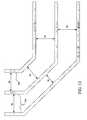
- FIGS. 12 and 13show details of the signal probe PCB.
- Signal lines 300are disposed on one side of a 1X thickness dielectric core 302 , with a power or ground plane 304 on the other side of the dielectric core 302 .
- the signal lines 300are spaced from 3X to 6X horizontal distance apart from one another. In the layers, the signal lines are spaced a vertical distance of 3X to 6X from an adjacent power or ground plane 304 associated with another set of signal lines 300 by dielectric and glue layer 306 .
- Adjacent power or ground planes 304are spaced a multiple of X distance vertically from each other by dielectric and glue layer 308 .
- Adjacent signal lines 300 associated with different power or ground planes 304are spaced apart a distance of 6X vertically from one another by dielectric and glue layer 310 . These spacing relationships minimize cross talk between adjacent conductors, and in the case of the thin separation between signal lines 300 and their associated power or ground planes 304 , the dielectric core 302 is thin in order to improve AC performance.
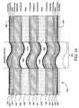
- the power probe PCB 106is rigid, except for the bendable section 107 that allows the power probe PCB 106 to be spaced away from the probe signal PCB 104 near the connections 109 (see also FIG. 3).
- the power probe PCB 106has a coverlay 320 on its top and bottom. Moving inward from the top and bottom, conductors 322 and 324 are respectively adjacent to the coverlays 320 .
- the conductors 322 and 324are separated from conductors 326 and 328 by glue layers 330 and 332 .
- Conductors 326 and 328are separated from conductors 334 and 336 by dielectric layers 338 and 340 .
- Conductors 334 and 336are separated from conductors 342 and 344 by glue layers 346 and 348 , except in the bendable section 107 , where the conductors 334 and 336 are separated from conductors 342 and 344 by voids 350 and 352 .
- the voids 350 and 352permit the bendable section 107 to flex.
- the conductors 342 and 344are separated from each other by dielectric layer 354 .
- FIGS. 15 - 16 Cshow a copper ground lug 400 used for a ground connection to the PCBs 104 and 106 , which are connected together by a high density board to board connector 402 .
- Alternate pins 404 of the connector 402are for signals and power.
- the presence of the ground lug 400 connected to traces on each boardprovides a good ground for both boards 104 and 106 , so that every third pin of the board to board connector does not need to be used for ground, as in the prior art.
- the high density board to board connector 402is implemented with a quad row staggered SMT socket assembly obtainable from Samtec USA. New Albany, Ind., under the designation SMT Socket Assembly.
- a similar SMT terminal assemblyis also used to connect flexible leads 158 (FIG. 10) to the PCB 104 .
- the ground lughas surface mount leads 406 and through hole post leads 408 .
- the through hole post leads 408serve to hold the two boards in registry with one another and allow screw 410 to be tightened without shearing the surface mount leads 406 from the boards 104 and 106 .
- the ground lug 400is also matched in height to the height of the board to board connector 402 . The ground lug therefore optimizes the use of the high density connector 402 and gives a good mechanical restraining device matched in height to the mating connector set.
Landscapes
- Engineering & Computer Science (AREA)
- Computer Hardware Design (AREA)
- Microelectronics & Electronic Packaging (AREA)
- General Engineering & Computer Science (AREA)
- Physics & Mathematics (AREA)
- General Physics & Mathematics (AREA)
- Environmental & Geological Engineering (AREA)
- Testing Of Individual Semiconductor Devices (AREA)
- Testing Or Measuring Of Semiconductors Or The Like (AREA)
- Tests Of Electronic Circuits (AREA)
Abstract
Description
- [0001] This invention was supported in part by grants from DARPA. The .U.S. Government may have rights in this invention.
- 1. Field of the Invention[0002]
- The present invention relates generally to a system and method for evaluation of integrated circuits and other semiconductor devices. More particularly, it relates a system incorporating hardware and suitable interconnections which allow efficient burn-in testing of a multiplicity of semiconductor devices while still incorporated in a semiconductor wafer. This invention is related to the inventions in commonly owned U.S. Pat. No. 5,429,510, issued to Barraclough et al. on Jul. 5, 1995, entitled “High-Density Interconnect Technique,” and commonly owned U.S. Pat. No. 5,682,472, issued to Brehm et al. on Oct. 28, 1997 and entitled “Method and System for Testing Memory Programming Devices,” the disclosures of which are hereby incorporated by reference herein. This invention is further related to the invention in a concurrently filed, copending, commonly owned application filed in the names of Frank[0003]0. Uher. Mark C. Carbone, John W. Andberg and Donald P. Richmond II, entitled “Wafer Level Burm-In and Test Cartridge” (Attorney Docket No. AEHR-006/00US), the disclosure of which is also incorporated by reference herein.
- 2. Description of the Prior Art[0004]
- When fabrication of integrated circuits and other semiconductor devices has been completed, the semiconductor devices are subjected to burn-in and electrical tests in order to identify and eliminate defective semiconductor devices before shipment to a customer. The term “burn-in” relates to operation of an integrated circuit at a predetermined temperature or temperature profile, typically an elevated temperature in an oven, a reduced temperature in an environmentally controlled enclosure, or a combination of an elevated temperature followed by a reduced temperature. Certain operating electrical bias levels and/or signals are supplied to the semiconductor devices while they are at the elevated temperature. The use of the elevated temperature or the combination of an elevated temperature followed by a reduced temperature accelerates stress to which the devices are subjected during burn-in, so that marginal devices that would otherwise fail shortly after being placed in service fail during burn-in and are eliminated before shipping. In electrical test, a more complete set of operating electrical bias levels and signals are supplied to the device to provide a thorough evaluation of its functions.[0005]
- As is apparent from the Brehm et al. patent, there are a variety of bum in and electrical test systems known in the art for burn-in and electrical test of integrated circuits and other semiconductor devices. To date, most of the prior art systems carry out the burn-in and electrical test after the integrated circuits have been separated into individual chips or die from a wafer in which they have been manufactured.[0006]
- More recently, interest has developed in wafer-level burn-in systems, some of which systems also include electrical test capability. In these systems, the integrated circuits undergo burn-in and may undergo electrical test prior to separation into individual integrated circuit chips.[0007]
- Wafer-level burn-in systems have attracted interest because they allow defective integrated circuits to be identified by the burn-in process before additional expense is incurred in their handling and packaging. Similarly, it is desirable to carry out electrical test of the integrated circuits while they are still in wafer form. Electrical test involves applying a suite of electrical signal inputs to each integrated circuit to make sure that it performs properly for its intended use.[0008]
- While the ability to carry out both burn-in and electrical test in a single wafer-level system is a highly desired result, there are significant interconnection, signal supply and power supply problems to be overcome before such a system can be implemented in practice. In a preferred implementation, the present invention is directed to solving those problems. In its broadest form, aspects of the present invention may, however, be employed in a system that carries out wafer-level burn-in or wafer-level electrical test alone.[0009]
- In accordance with one aspect of the invention, a burn-in test system includes a device under test zone configured to receive a plurality of cartridges each containing a semiconductor wafer including a plurality of integrated circuits. Each of the plurality of cartridges includes a rigid probe signal printed circuit board and a probe power printed circuit board substantially parallel to and closely spaced from the rigid probe printed circuit board. Test electronics are positioned adjacent to the device under test zone. Power electronics are positioned adjacent to said device under test zone. A first interconnection system connects the test electronics to the rigid probe signal printed circuit board. A second interconnection system connects the power electronics to the probe power printed circuit board. The first and second interconnection systems are arranged in a stacked relationship. The probe power printed circuit board has at least a bendable section permitting a portion of the probe power printed circuit board to be spaced a greater distance away from the rigid probe signal printed circuit board proximate to the second interconnection system.[0010]
- In accordance with a second aspect of the invention, a test system includes a device under test zone configured to receive a plurality of cartridges each containing a semiconductor wafer including a plurality of integrated circuits. Each of the plurality of cartridges includes a rigid probe signal printed circuit board and a probe power printed circuit board substantially parallel to and closely spaced from the rigid probe printed circuit board. Test electronics are positioned adjacent to said device under test zone. Power electronics are positioned adjacent to the device under test zone. A first interconnection system connects the test electronics to the rigid probe signal printed circuit board. A second interconnection system connects the power electronics to the probe power printed circuit board. The first and second interconnection systems are arranged in a stacked relationship. The probe power printed circuit board has at least a bendable section permitting a portion of the probe power printed circuit board to be spaced a greater distance away from the rigid probe signal printed circuit board proximate to the second interconnection system.[0011]
- In a third aspect of the invention, a burn-in system has a temperature controlled zone configured to receive a plurality of cartridges each containing a semiconductor wafer including a plurality of integrated circuits. Test electronics are positioned in a cool zone. Power electronics are positioned in the cool zone. A transition zone separates the temperature controlled zone and the cool zone.[0012]
- In a fourth aspect of the invention, a test system includes a device under test zone configured to receive a plurality of cartridges each containing a semiconductor wafer including a plurality of integrated circuits. Test electronics on a first circuit board are positioned adjacent to the device under test zone. Power electronics on a second circuit board are positioned adjacent to said device under test zone. Each of the plurality of cartridges are connected to the test electronics by a first connection between one of the plurality of cartridges and the first circuit board and to the power electronics by a second connection between the one of said plurality of cartridges and the second circuit board separate from the first connection.[0013]
- In a fifth aspect of the invention, a test system includes a first plurality of test channels each adapted to receive a second plurality of integrated circuits under test. A second plurality of power modules are each connected to one of the integrated circuits under test in each test channel. A controller is connected and configured for successive selection of one of the first plurality of test channels.[0014]
- In a sixth aspect of the invention, a method for burn-in testing integrated circuits in wafer form includes providing a temperature controlled zone configured to receive a plurality of cartridges each containing a semiconductor wafer including a plurality of integrated circuits. The integrated circuits are tested with test electronics positioned in a cool zone. Power is provided to the integrated circuits with power electronics positioned in the cool zone. The test and power electronics are separated from the temperature controlled zone with a transition zone between the temperature controlled zone and the cool zone.[0015]
- In a seventh aspect of the invention, a method for testing integrated circuits in wafer form includes connecting a first plurality of integrated circuits in a second plurality of test channels. A first plurality of power modules is connected to one of the integrated circuits under test in each test channel. One of the second plurality of test channels is selectively selected. The first plurality of the integrated circuits in the selected test channel is tested. The selective selection and testing steps are repeated until all of the integrated circuits have been tested.[0016]
- In reviewing the following more detailed description and drawings of the present invention the advantages and features of the invention should be more readily apparent to those skilled in the art.[0017]
- FIG. 1 is a block diagram and schematic representation of an embodiment of a burn-in and electrical test system in accordance with the invention.[0018]
- FIG. 2 is a block diagram and schematic representation of part of the system shown in FIG. 1.[0019]
- FIG. 3 is another more detailed block diagram and schematic representation of the part of the system shown in FIG. 2.[0020]
- FIG. 4 is a partially exploded block diagram of the part of the system shown in FIG. 3.[0021]
- FIG. 4A is a cross section view of an interconnection system used in the part of the system portion shown in FIG. 2.[0022]
- FIG. 5 is a block diagram of another part of the system shown in FIGS.[0023]1-4.
- FIGS. 6 and 7 are circuit diagrams of a portion of the system part of FIG. 5.[0024]
- FIGS. 8 and 9 are pinout connection diagrams of integrated circuits under burn-in and test using the invention.[0025]
- FIGS. 10 and 11 are somewhat schematic representations of interconnections used in the system portion shown in FIGS.[0026]2-4.
- FIG. 12 is a cross section view of a portion of the interconnections shown in FIG. 10.[0027]
- FIG. 13 is a plan view of a portion of the interconnections shown in FIG. 10.[0028]
- FIG. 14 is a cross section view of a portion of the interconnections shown in FIG. 11.[0029]
- FIG. 15 is a cross section view of one of the interconnections in the system portion shown in FIGS.[0030]2-4.
- FIGS. 16A.[0031]16B and16C are perspective, top and side views of a part of the interconnection shown in FIG. 15.
- Turning now to FIG. 1, there is shown a burn-in and[0032]
electrical test system 20 in accordance with the invention. As shown, alocal controller 21 is connected to a plurality of electricaltest zones # 1 through #n via aninternal Ethernet network 101. Electricaltest zone # 1 shows the details of each electrical test zone. Each of the electrical test zones has a singletest pattern generator 103 connected by aparallel bus 105 to a plurality oftest slots 107 comprising atest slot interface 119. Eachtest slot 107 comprisesoptional fault analysis 109, adriver comparator board 111 and a wafer/diepower system 113. Two separate connections for eachwafer test cartridge 26 for test electronics and for power distribution are represented at115 and117. Theoptional fault analysis 109 anddriver comparator board 111 comprise the test electronics and are connected to thewafer test cartridge 26 byconnection 115. The wafer/diepower system 113 is connected to thewafer test cartridge 26 byconnection 117. - FIG. 2 shows a portion of the[0033]
system 20 of FIG. 1. A plurality ofwafer cartridges 26 are connected to testelectronics 28 andpower electronics 30. Thetest electronics 28 comprises a single pattern generator printed circuit board (PCB)29 and separate signal driver andfault analysis PCBs 33 for eachwafer cartridge 26. Each of thewafer cartridges 26 contains a semiconductor wafer incorporating a plurality of integrated circuits. All of the signal driver andfault analysis PCBs 33 are connected to the pattern generator PCB byparallel bus 105. Further details of thecartridges 26 are contained in a concurrently filed, co-owned pending application entitled “Wafer Level Burn-In and Test Cartridge and Alignment Method,” filed in the names of Frank O. Uher, Mark C. Carbone, John W. Andberg and Donald P. Richmond II (Attorney Docket No. AEHR-006/00US), the disclosure of which is hereby incorporated by reference herein. Some aspects of thecartridge 26 will be described below as necessary for a more complete understanding of the present invention. - FIGS. 3 and 4 show further details of the[0034]
wafer cartridge 26.test electronics 28 andpower electronics 30 and how they are interconnected. As shown in FIG. 3, thetest electronics 28 consists of apattern generator PCB 29 and a signal driver andfault analysis PCB 33 connected together by theparallel bus 105. Thefault analysis PCB 33 is connected to a rigidsignal probe PCB 104 incartridge 26 through adriver extender PCB 102 to provide a straight through signal path. Theprobe PCB 104 is rigid in order to allow close control of impedance between each signal line and a backplane, to be discussed more fully below in connection with FIGS. 10, 12 and13, thus providing impedance controlled interconnections between a semiconductor wafer under test and thetest electronics 28. - The portion of the[0035]
system 20 shown in FIGS. 3 and 4 is divided into a temperature controlledzone 22, a cool orambient temperature zone 24 and atransition zone 25. The temperature controlled zone is either heated to an elevated temperature, such as 150° C., or chilled, such as to a temperature of 0° C. during the burn-in or test operation. Thewafer cartridge 26 extends from the temperature controlledzone 22 into thetransition zone 25. Athermal dam 156 is positioned around thewafer cartridge 26 at the interface between the temperature controlled zone and the transition zone to minimize heat transfer between the zones around thecartridge 26. Thetransition zone 25 is provided in order to prevent heat or cold leakage from the controlled temperature zone into the signal driver andfault analysis PCB 33. Such heat or cold leakage would change the temperature of thePCB 33 over time, thus causing a performance chance, resulting in a variation of test conditions over time. Additionally, cold leakage into thePCB 33 would result in condensation or thermal damage to thePCB 33. - The[0036]
driver extender PCB 102 serves to space the signal driver andfault analysis PCB 33 from the temperature controlledzone 22 and thetransition zone 25 for further heat and cold isolation. Additionally, thedriver extender PCB 102 permits impedance matching of the signal probe PCB and the signal driver andfault analysis PCB 33. In practice, thesignal probe PCB 104 has an impedance of about 50 ohm, and the signal driver andfault analysis PCB 33 has an impedance of about 28 ohm. The driver extender PCB has a varying impedance along its length, from about 28 ohm on the signal driver andfault analysis PCB 33 end to about 50 ohm on thesignal probe PCB 104 end. This impedance matching permits higher quality signals to be transmitted between the signal driver andfault analysis PCB 33 and thesignal probe PCB 104. - The[0037]
power distribution system 30 is connected to aprobe power PCB 106 in thecartridge 26. Theprobe PCB 106 has aflexible portion 107 order to allow it to be positioned closely adjacent to and parallel with therigid probe PCB 104 along most of its extent in thecartridge 26, yet extend a substantial distance away from theprobe PCB 106 at its interconnection with thepower distribution system 30. - The[0038]
cartridge 26 is connected to thetest electronics 28 and thepower distribution system 30 through amini-backplane PCB 108. Highpin density connectors 109 are used to connect thecartridge 26 to thedriver extender PCB 102 and to thepower distribution system 30. Theconnectors 109 include a total of 4200 pin connections, compared with a total of 680 pin connections in the system described in the above-referenced Brehm et al. patent. The connectors have insulated pins and the signal pins are set in an electromagnetic interference (EMI) shield housing. Suitable highpin density connectors 109 of this type are commercially available from AMP Incorporated, Harrisburg, Pa. and will not be further described herein. - The[0039]
power distribution system 30 includes a die powermain PCB 110 and aset 118 of 32-channel die power dual-in-line modules (DIMs) mounted on the die powermain PCB 110. In thetest electronics 28, thedriver extender board 102 is connected to a mainsignal driver PCB 33 by aninterconnection system 31. Aset 120 of signal driver DIMs and afault analysis PCB 114 are mounted on the mainsignal driver PCB 33. - FIG. 4A shows details of the[0040]
interconnection 31. This interconnection system is the subject of the above-referenced Barraclough et al. patent. - The[0041]
system 31 employscontact fingers 32 on bothsurfaces PCB 102 andPCB 33. Each of thePCBs edge connector contact fingers 32 and the card-edge connectors edge connector 44 of thePCB 102 mates withcontact fingers 32 of thePCB 33, and the card-edge connector 46 of thePCB 33 mates with the contact fingers of thePCB 102. ThePCB 102 has twosets 70 and72 of interconnections connected tometal contacts 74 of the card-edge connector 44 and two sets of76 and78 of interconnections connected to contactfingers 32 of thePCB 33. Similarly,PCB 33 has twosets fingers 32 of thePCB 33 and twosets metal contacts 88 of the card-edge connector 46. With thisinterconnection system 31 there is twice the density of interconnects per inch using the same card-edge connector compared with a typical prior art interconnection system, for example. 40 interconnects per inch of card edge between two PCBs, compared with 20 interconnects per inch in the prior art example. - Besides doubling the number of interconnects, the[0042]
interconnection system 31 is self-aligning. The card-edge connectors connectors connectors connectors - FIG. 5 shows the parallel test processing capability and segmented power distribution of the[0043]
system 20. Eachpower module 280 is connected to 32 devices undertest 200 comprising 32 channels. While carrying out the testing, only one of the 32 channels is made active at a time using the chip select lines282. This means that only one device undertest 200 is powered by eachpower module 280 at a time, thus resulting in far less need for capacitance perpower module 280. In practice, power is supplied to all of thedevices 200 under test in their inactive state, but only one device per power module is powered to its active state at a time. The active state uses power at a much higher level and makes much more electrical noise on the power lines. The capacitance in each power module is provided to satisfy current demand when cycling from low to high power demand at high frequencies. There are a total of 32 power modules, but only 8 are shown in FIG. 10. This segmented mode of power distribution is far more manageable than attempting to power all of the devices under test at once. - FIG. 6 shows a circuit schematic of the[0044]
power module 280. Thepower module 280 has amicrocontrol element 252 connected at254 to control turning on and turning off an MOSFET power switch 256. Themicrocontrol element 252 can be implemented as an microcontroller, a field programmable gate array (FPGA) or a Cypress progammable logic device (CPLD). AVdd input 253 is connected to input255 of thepower switch 256.Output 258 of thepower switch 256 is connected to the device under test (DUT)200. Themicrocontrol element 252 is also connected to an analog to digital (A/D)converter 260 by an A/D bus 262, to achannel multiplexer 264 by a multiplexedbus 266 and to a voltage—current measurement multiplexer 268 by the multiplexedbus 266. Input270 of the A/D converter 260 is connected to the voltage—current measurement multiplexer 268.Outputs 272 of thechannel multiplexer 264 are connected through aninstrumentation amplifier 274 to the voltage—current multiplexer 268. One of theoutputs 272 on theDUT 200 side of R connects directly to the voltage—current multiplexer 268. Themicrocontrol element 252 is connected by a microprocessor bus276 to a microprocessor on thesignal driver PCB 33. (see also FIGS.2-4). That microprocessor is an intermediate level of control between themicrocontrol element 252 and another microprocessor in the local controller21 (FIG. 1). Anasynchronous clock input 255 is connected to themicrocontrol element 252. - In operation, the[0045]
microcontrol element 252 controls the supply of power to thedevices 200 under test by sequencing thechannel multiplexer 264 through channels1-32 (see also FIG. 5). When eachDUT 200 is powered, the microcontrol element controls the voltage—current multiplexer 268 to cycle between voltage and current measurements. The voltage and current inputs from theDUT 200 are supplied through the channel multiplexer to the voltage—current multiplexer 268. The A/D converter 260 converts to digital, and themicrocontrol element 252 receives, the voltage and current measurements and compares those measurements against the programmed high and low limits in order to detect an under or over voltage or under or over current condition. When any is detected, thepower switch 256 is turned off before damage to a probe contacting theDUT 200 can take place. The significance of local control by themicrocontrol element 252 is its speed of operation. The two measurements to detect voltage and current take place within the time of about 3 milliseconds it takespower switch 256 to switch from an off to an on state. This speed of operation protects thewafer DUT 200 and the wafer probe either when failure of theDUT 200 takes place while it is under test or when the device first turns on. - FIG. 7 shows another embodiment of a[0046]
power module 280 in the form of a power regulator control and voltage/current readback circuit 210. AVdd reference input 212 is supplied throughresistor network 214 to power control transistor T1 and adjustinput 216 of an adjustable regulator integratedcircuit 218. Araw power input 219 is also connected to theintegrated circuit 218. Output220 of theintegrated circuit 218 is connected to the device undertest 200. Anoutput 236 of themicrocontrol element 252 is connected throughresistor network 238 to the base of power control transistor T1. In operation, theadjustable regulator 218 attempts to adjust the raw power input at219 to be equal to the reference at216. When the power control transistor T1 is turned on by themicrocontrol element 252, transistor T1 pulls down the adjustinput 216 to the adjustable regulator integratedcircuit 218, shutting it off. Thecircuit 210 allows custom regulation of the test voltage to eachDUT 200, thus improving the accuracy of the test voltage to each device. Other than as shown and described, the construction and operation of the FIG. 7 circuit is the same as that of the FIG. 6 circuit. - FIGS. 8 and 9 respectively show an example of signal and power connections to a Rambus dynamic random access memory (RDRAM)[0047]
integrated circuit 200 and a general example of a memory integratedcircuit 200 on a semiconductor wafer. As shown,connections 202 include a capacitance of 0.1 to 5 μfarad for each connection.Connections 204 and two of theinterconnections 202 include a resistance of 200 to 800 ohm for each connection.Connections 206 include a resistance of 20 to 80 ohm. The resistances R and R1 are provided for isolation to allow tolerating failure of any oneintegrated circuit 200 under test of a semiconductor wafer. The difference between R and R1 is because theintegrated circuits 200 under test have a low ability to drive capacitance and the resistance R1 therefore needs to be lower to give an appropriate RC constant. In the interconnections of thecartridge 26 and the various PCBs, the connections to theintegrated circuit 200 are bussed together as indicated. - Further details of the[0048]
wafer cartridge 26 are shown in FIGS.10-14. Aprobe 150 is centrally disposed on theprobe PCB 104. Theprobe 150 has a plurality oftiles 152 that contain a multiplicity of contacts (not shown) for contacting each of the integrated circuits in a semiconductor wafer. Theprobe 150 is mounted on acontactor 151. When the wafer cartridge is loaded into the burn-in and electrical test system (see FIGS.2-4), theportions 154 of the interconnections109 (see also FIGS. 3 and 4) that is attached to thecartridge 26 attach to the rest ofinterconnections 109 on themini-backplane PCB 108. The signal connections in theportion 154 comprise insulated pins that are set in an electromagnetic interference (EMI) shield housing.Flexible interconnections 158 electrically connect thecontactor 151 to thesignal probe PCB 104 and thepower probe PCB 106. Since thecontactor 151, theprobe signal PCB 104 and theprobe power PCB 106 are rigid and are made of different materials, theflexible interconnections 158 allow for differential expansion of theprobe 150,probe signal PCB 104 and probepower PCB 106 when they are heated during burn-in. - FIGS. 12 and 13 show details of the signal probe PCB.[0049]
Signal lines 300 are disposed on one side of a 1X thicknessdielectric core 302, with a power orground plane 304 on the other side of thedielectric core 302. The signal lines300 are spaced from 3X to 6X horizontal distance apart from one another. In the layers, the signal lines are spaced a vertical distance of 3X to 6X from an adjacent power orground plane 304 associated with another set ofsignal lines 300 by dielectric andglue layer 306. Adjacent power orground planes 304 are spaced a multiple of X distance vertically from each other by dielectric andglue layer 308.Adjacent signal lines 300 associated with different power orground planes 304 are spaced apart a distance of 6X vertically from one another by dielectric andglue layer 310. These spacing relationships minimize cross talk between adjacent conductors, and in the case of the thin separation betweensignal lines 300 and their associated power orground planes 304, thedielectric core 302 is thin in order to improve AC performance. - Details of the[0050]
power probe PCB 106 are shown in FIG. 14. Thepower probe PCB 106 is rigid, except for thebendable section 107 that allows thepower probe PCB 106 to be spaced away from theprobe signal PCB 104 near the connections109 (see also FIG. 3). Thepower probe PCB 106 has acoverlay 320 on its top and bottom. Moving inward from the top and bottom,conductors coverlays 320. Theconductors conductors 326 and328 byglue layers Conductors 326 and328 are separated fromconductors dielectric layers Conductors conductors glue layers bendable section 107, where theconductors conductors voids voids bendable section 107 to flex. Theconductors dielectric layer 354. - FIGS.[0051]15-16C show a
copper ground lug 400 used for a ground connection to thePCBs Alternate pins 404 of the connector402 are for signals and power. The presence of theground lug 400 connected to traces on each board provides a good ground for bothboards PCB 104. The ground lug has surface mount leads406 and through hole post leads408. The through hole post leads408 serve to hold the two boards in registry with one another and allowscrew 410 to be tightened without shearing the surface mount leads406 from theboards ground lug 400 is also matched in height to the height of the board to board connector402. The ground lug therefore optimizes the use of the high density connector402 and gives a good mechanical restraining device matched in height to the mating connector set. - It should be apparent to those skilled in the art that various changes in form and details of the invention as shown and described may be made. It is intended that such changes be included within the spirit and scope of the claims appended hereto.[0052]
Claims (26)
Priority Applications (2)
| Application Number | Priority Date | Filing Date | Title |
|---|---|---|---|
| US10/718,825US7619428B2 (en) | 1999-07-14 | 2003-11-21 | Wafer level burn-in and electrical test system and method |
| US12/574,447US7928754B2 (en) | 1999-07-14 | 2009-10-06 | Wafer level burn-in and electrical test system and method |
Applications Claiming Priority (3)
| Application Number | Priority Date | Filing Date | Title |
|---|---|---|---|
| US09/353,121US6562636B1 (en) | 1999-07-14 | 1999-07-14 | Wafer level burn-in and electrical test system and method |
| US09/865,957US6682945B2 (en) | 1999-07-14 | 2001-05-25 | Wafer level burn-in and electrical test system and method |
| US10/718,825US7619428B2 (en) | 1999-07-14 | 2003-11-21 | Wafer level burn-in and electrical test system and method |
Related Parent Applications (1)
| Application Number | Title | Priority Date | Filing Date |
|---|---|---|---|
| US09/865,957ContinuationUS6682945B2 (en) | 1999-07-14 | 2001-05-25 | Wafer level burn-in and electrical test system and method |
Related Child Applications (1)
| Application Number | Title | Priority Date | Filing Date |
|---|---|---|---|
| US12/574,447ContinuationUS7928754B2 (en) | 1999-07-14 | 2009-10-06 | Wafer level burn-in and electrical test system and method |
Publications (2)
| Publication Number | Publication Date |
|---|---|
| US20040113645A1true US20040113645A1 (en) | 2004-06-17 |
| US7619428B2 US7619428B2 (en) | 2009-11-17 |
Family
ID=23387847
Family Applications (4)
| Application Number | Title | Priority Date | Filing Date |
|---|---|---|---|
| US09/353,121Expired - LifetimeUS6562636B1 (en) | 1999-07-14 | 1999-07-14 | Wafer level burn-in and electrical test system and method |
| US09/865,957Expired - LifetimeUS6682945B2 (en) | 1999-07-14 | 2001-05-25 | Wafer level burn-in and electrical test system and method |
| US10/718,825Expired - Fee RelatedUS7619428B2 (en) | 1999-07-14 | 2003-11-21 | Wafer level burn-in and electrical test system and method |
| US12/574,447Expired - Fee RelatedUS7928754B2 (en) | 1999-07-14 | 2009-10-06 | Wafer level burn-in and electrical test system and method |
Family Applications Before (2)
| Application Number | Title | Priority Date | Filing Date |
|---|---|---|---|
| US09/353,121Expired - LifetimeUS6562636B1 (en) | 1999-07-14 | 1999-07-14 | Wafer level burn-in and electrical test system and method |
| US09/865,957Expired - LifetimeUS6682945B2 (en) | 1999-07-14 | 2001-05-25 | Wafer level burn-in and electrical test system and method |
Family Applications After (1)
| Application Number | Title | Priority Date | Filing Date |
|---|---|---|---|
| US12/574,447Expired - Fee RelatedUS7928754B2 (en) | 1999-07-14 | 2009-10-06 | Wafer level burn-in and electrical test system and method |
Country Status (1)
| Country | Link |
|---|---|
| US (4) | US6562636B1 (en) |
Cited By (11)
| Publication number | Priority date | Publication date | Assignee | Title |
|---|---|---|---|---|
| US20050134163A1 (en)* | 2003-12-08 | 2005-06-23 | William Voorhees | Parallel bus debugging tool |
| US20060126248A1 (en)* | 2004-12-09 | 2006-06-15 | Samsung Electronics Co., Ltd. | Method and apparatus for controlling device power supply in semiconductor tester |
| US20100213957A1 (en)* | 2005-04-27 | 2010-08-26 | Aehr Test Systems | Apparatus for testing electronic devices |
| US7928754B2 (en) | 1999-07-14 | 2011-04-19 | Aehr Test Systems | Wafer level burn-in and electrical test system and method |
| CN106568990A (en)* | 2016-10-31 | 2017-04-19 | 宁波舜宇光电信息有限公司 | Probe testing device of electronic module |
| KR102319160B1 (en)* | 2020-07-14 | 2021-11-01 | 주식회사 엑시콘 | Semiconductor device test system |
| US11448695B2 (en) | 2007-12-19 | 2022-09-20 | Aehr Test Systems | System for testing an integrated circuit of a device and its method of use |
| US11635459B2 (en) | 2017-03-03 | 2023-04-25 | Aehr Test Systems | Electronics tester |
| US11835575B2 (en) | 2020-10-07 | 2023-12-05 | Aehr Test Systems | Electronics tester |
| US12007451B2 (en) | 2016-01-08 | 2024-06-11 | Aehr Test Systems | Method and system for thermal control of devices in an electronics tester |
| US12298328B2 (en) | 2009-03-25 | 2025-05-13 | Aehr Test Systems | Controlling alignment during a thermal cycle |
Families Citing this family (28)
| Publication number | Priority date | Publication date | Assignee | Title |
|---|---|---|---|---|
| US7222041B2 (en)* | 2001-11-08 | 2007-05-22 | Teradyne, Inc. | High-speed digital multiplexer |
| US6787375B2 (en)* | 2002-05-13 | 2004-09-07 | Taiwan Semiconductor Manufacturing Co., Ltd | Microelectronic fabrication die electrical test method providing enhanced microelectronic fabrication die electrical test efficiency |
| US6732352B2 (en)* | 2002-05-23 | 2004-05-04 | Hewlett-Packard Development Company, L.P. | System and method for creating probe masks |
| US6677172B1 (en)* | 2002-06-27 | 2004-01-13 | Emcore Corporation | On-wafer burn-in of semiconductor devices using thermal rollover |
| US6815966B1 (en)* | 2002-06-27 | 2004-11-09 | Aehr Test Systems | System for burn-in testing of electronic devices |
| US7019676B2 (en)* | 2003-06-12 | 2006-03-28 | Matsushita Electric Industrial Co, Ltd. | D/A converter |
| US7279703B2 (en)* | 2003-08-14 | 2007-10-09 | Intel Corporation | Self-heating burn-in |
| US7135704B2 (en)* | 2003-08-14 | 2006-11-14 | Lockhead Martin Corporation | VCSEL settling fixture |
| US7802141B2 (en)* | 2004-03-05 | 2010-09-21 | Denso Corporation | Semiconductor device having one-chip microcomputer and over-voltage application testing method |
| US7245134B2 (en)* | 2005-01-31 | 2007-07-17 | Formfactor, Inc. | Probe card assembly including a programmable device to selectively route signals from channels of a test system controller to probes |
| WO2006102420A2 (en)* | 2005-03-21 | 2006-09-28 | Defibtech, Llc | Pcb blade connector system and method |
| US7633307B2 (en)* | 2005-12-16 | 2009-12-15 | Freescale Semiconductor, Inc. | Method for determining temperature profile in semiconductor manufacturing test |
| JP4477044B2 (en)* | 2007-06-25 | 2010-06-09 | 株式会社東芝 | Manufacturing method of semiconductor device |
| US8134380B2 (en)* | 2008-11-26 | 2012-03-13 | Taiwan Semiconductor Manufacturing Company, Ltd. | Test probe structure |
| TWI431852B (en)* | 2009-07-16 | 2014-03-21 | Hon Hai Prec Ind Co Ltd | Electrical connector and combination thereof |
| TWI465737B (en)* | 2012-08-14 | 2014-12-21 | Accton Technology Corp | Burn-in test system |
| US8937794B2 (en)* | 2012-09-28 | 2015-01-20 | Intel Corporation | Sort probe over current protection mechanism |
| JP6351442B2 (en)* | 2014-08-28 | 2018-07-04 | ルネサスエレクトロニクス株式会社 | Semiconductor test equipment |
| CN106873195B (en)* | 2015-12-11 | 2020-10-30 | De&T株式会社 | Probe unit replacement device |
| US10147676B1 (en) | 2017-05-15 | 2018-12-04 | International Business Machines Corporation | Wafer-scale power delivery |
| TWI704360B (en)* | 2019-07-09 | 2020-09-11 | 致茂電子股份有限公司 | Wafer testing device of flip chip vcsel |
| EP4084052A4 (en)* | 2020-01-19 | 2022-11-30 | Huawei Technologies Co., Ltd. | WAFER WITH WAFER STRUCTURE AND TEST METHOD THEREOF, AND HIGH BANDWIDTH MEMORY AND MANUFACTURING METHOD THEREOF |
| TWI745913B (en)* | 2020-04-01 | 2021-11-11 | 美商第一檢測有限公司 | System-level test equipment and system-level test system |
| TWI759833B (en)* | 2020-08-25 | 2022-04-01 | 伊士博國際商業股份有限公司 | Burn-in apparatus with functional testing for processor |
| CN114944187B (en)* | 2022-06-20 | 2025-10-03 | 西安微电子技术研究所 | An aging test system for TSV reconstructed stacked memory |
| CN115144722B (en)* | 2022-07-27 | 2023-02-28 | 镭神技术(深圳)有限公司 | Aging equipment and aging test method for miniature semiconductor refrigerating sheet |
| US11893253B1 (en)* | 2022-09-20 | 2024-02-06 | Western Digital Technologies, Inc. | Dynamic TD-PPM state and die mapping in multi-NAND channels |
| CN119644093A (en)* | 2023-09-15 | 2025-03-18 | 芯卓科技(浙江)有限公司 | Wafer test box |
Citations (50)
| Publication number | Priority date | Publication date | Assignee | Title |
|---|---|---|---|---|
| US3530750A (en)* | 1968-01-05 | 1970-09-29 | Houdaille Industries Inc | Punching tool assembly |
| US4258620A (en)* | 1978-04-18 | 1981-03-31 | Hakan Sallander | Tool fastening means for a press |
| US4374317A (en)* | 1979-07-05 | 1983-02-15 | Reliability, Inc. | Burn-in chamber |
| US4577847A (en)* | 1983-04-12 | 1986-03-25 | Schedwin Sven Erik | Clamping device |
| US4662043A (en)* | 1985-01-10 | 1987-05-05 | Sheffer Collet Company | Project plate system |
| US4818933A (en)* | 1986-10-08 | 1989-04-04 | Hewlett-Packard Company | Board fixturing system |
| US5103168A (en)* | 1988-10-27 | 1992-04-07 | Grumman Aerospace Corporation | Stress testing equipment with an integral cooling plenum |
| US5174772A (en)* | 1992-01-22 | 1992-12-29 | The United States Of America As Represented By The Administrator Of The National Aeronautics & Space Administration | Work attachment mechanism/work attachment fixture |
| US5385487A (en)* | 1993-08-30 | 1995-01-31 | At&T Corp. | Apparatus for electrically operating devices in a controlled environment |
| US5399505A (en)* | 1993-07-23 | 1995-03-21 | Motorola, Inc. | Method and apparatus for performing wafer level testing of integrated circuit dice |
| US5429510A (en)* | 1993-12-01 | 1995-07-04 | Aehr Test Systems, Inc. | High-density interconnect technique |
| US5510724A (en)* | 1993-05-31 | 1996-04-23 | Tokyo Electron Limited | Probe apparatus and burn-in apparatus |
| US5568054A (en)* | 1992-07-31 | 1996-10-22 | Tokyo Electron Limited | Probe apparatus having burn-in test function |
| US5570032A (en)* | 1993-08-17 | 1996-10-29 | Micron Technology, Inc. | Wafer scale burn-in apparatus and process |
| US5593903A (en)* | 1996-03-04 | 1997-01-14 | Motorola, Inc. | Method of forming contact pads for wafer level testing and burn-in of semiconductor dice |
| US5597737A (en)* | 1995-11-03 | 1997-01-28 | Motorola Inc. | Method for testing and burning-in a semiconductor wafer |
| US5600257A (en)* | 1995-08-09 | 1997-02-04 | International Business Machines Corporation | Semiconductor wafer test and burn-in |
| US5621313A (en)* | 1993-09-09 | 1997-04-15 | Tokyo Seimitsu Co., Ltd. | Wafer probing system and method that stores reference pattern and movement value data for different kinds of wafers |
| US5654588A (en)* | 1993-07-23 | 1997-08-05 | Motorola Inc. | Apparatus for performing wafer-level testing of integrated circuits where the wafer uses a segmented conductive top-layer bus structure |
| US5656943A (en)* | 1995-10-30 | 1997-08-12 | Motorola, Inc. | Apparatus for forming a test stack for semiconductor wafer probing and method for using the same |
| US5682472A (en)* | 1995-03-17 | 1997-10-28 | Aehr Test Systems | Method and system for testing memory programming devices |
| US5701666A (en)* | 1994-08-31 | 1997-12-30 | Motorola, Inc. | Method for manufacturing a stimulus wafer for use in a wafer-to-wafer testing system to test integrated circuits located on a product wafer |
| US5743324A (en)* | 1994-06-10 | 1998-04-28 | Rotelec | Disconnectable electrical connection system for a moving assembly |
| US5777485A (en)* | 1995-03-20 | 1998-07-07 | Tokyo Electron Limited | Probe method and apparatus with improved probe contact |
| US5808474A (en)* | 1994-11-30 | 1998-09-15 | Lsi Logic Corporation | Test socket for testing integrated circuit packages |
| US5834946A (en)* | 1995-10-19 | 1998-11-10 | Mosaid Technologies Incorporated | Integrated circuit test head |
| US5859539A (en)* | 1990-08-29 | 1999-01-12 | Micron Technology, Inc. | Universal wafer carrier for wafer level die burn-in |
| US5894218A (en)* | 1994-04-18 | 1999-04-13 | Micron Technology, Inc. | Method and apparatus for automatically positioning electronic dice within component packages |
| US5945834A (en)* | 1993-12-16 | 1999-08-31 | Matsushita Electric Industrial Co., Ltd. | Semiconductor wafer package, method and apparatus for connecting testing IC terminals of semiconductor wafer and probe terminals, testing method of a semiconductor integrated circuit, probe card and its manufacturing method |
| US5954932A (en)* | 1991-02-28 | 1999-09-21 | Hitachi, Ltd. | DNA detector and DNA detection method |
| US6066181A (en)* | 1997-12-08 | 2000-05-23 | Analysis & Technology, Inc. | Java native interface code generator |
| US6084215A (en)* | 1997-11-05 | 2000-07-04 | Tokyo Electron Limited | Semiconductor wafer holder with spring-mounted temperature measurement apparatus disposed therein |
| US6133054A (en)* | 1999-08-02 | 2000-10-17 | Motorola, Inc. | Method and apparatus for testing an integrated circuit |
| US6140616A (en)* | 1998-09-25 | 2000-10-31 | Aehr Test Systems | Wafer level burn-in and test thermal chuck and method |
| US6144210A (en)* | 1998-06-09 | 2000-11-07 | Zen Licensing Group, Llp | Method and apparatus for finding and locating manufacturing defects on a printed circuit board |
| US6147605A (en)* | 1998-09-11 | 2000-11-14 | Motorola, Inc. | Method and apparatus for an optimized circuit for an electrostatic radio frequency identification tag |
| US6147506A (en)* | 1997-04-29 | 2000-11-14 | International Business Machines Corporation | Wafer test fixture using a biasing bladder and methodology |
| US6205652B1 (en)* | 1998-06-02 | 2001-03-27 | Tokyo Electron Limited | Vacuum coupling system |
| US6340895B1 (en)* | 1999-07-14 | 2002-01-22 | Aehr Test Systems, Inc. | Wafer-level burn-in and test cartridge |
| US6377471B1 (en)* | 2000-11-06 | 2002-04-23 | Sun Microsystems, Inc. | Disk drive interface with variably spaceable connectors |
| US6413113B2 (en)* | 1999-07-14 | 2002-07-02 | Aehr Test Systems | Kinematic coupling |
| US6420766B1 (en)* | 1997-07-17 | 2002-07-16 | International Business Machines Corporation | Transistor having raised source and drain |
| US6426638B1 (en)* | 2000-05-02 | 2002-07-30 | Decision Track Llc | Compliant probe apparatus |
| US6426904B2 (en)* | 1998-11-13 | 2002-07-30 | International Business Machines Corporation | Structures for wafer level test and burn-in |
| US6433419B2 (en)* | 1990-09-24 | 2002-08-13 | Tessera, Inc. | Face-up semiconductor chip assemblies |
| US6441116B1 (en)* | 1997-09-03 | 2002-08-27 | Idemitsu Kosan Co., Ltd. | Ethylenic copolymer, composition containing said copolymer, and ethylenic copolymer film |
| US6562636B1 (en)* | 1999-07-14 | 2003-05-13 | Aehr Test Systems | Wafer level burn-in and electrical test system and method |
| US6640323B2 (en)* | 1998-01-21 | 2003-10-28 | Micron Technology, Inc. | Testing system for evaluating integrated circuits, a testing system, and a method for testing an integrated circuit |
| US7063544B2 (en)* | 2002-06-27 | 2006-06-20 | Aehr Test Systems | System for burn-in testing of electronic devices |
| US7208968B2 (en)* | 2003-06-11 | 2007-04-24 | Infineon Technologies Ag | Test system for testing integrated chips and an adapter element for a test system |
Family Cites Families (16)
| Publication number | Priority date | Publication date | Assignee | Title |
|---|---|---|---|---|
| DE3882158T2 (en) | 1987-03-11 | 1994-01-27 | Hewlett Packard Co | Device for automatically cleaning a surface. |
| US5389556A (en)* | 1992-07-02 | 1995-02-14 | Lsi Logic Corporation | Individually powering-up unsingulated dies on a wafer |
| US5442282A (en) | 1992-07-02 | 1995-08-15 | Lsi Logic Corporation | Testing and exercising individual, unsingulated dies on a wafer |
| JP3108398B2 (en) | 1993-12-21 | 2000-11-13 | 松下電器産業株式会社 | Method of manufacturing probe card |
| JP2925964B2 (en) | 1994-04-21 | 1999-07-28 | 松下電器産業株式会社 | Semiconductor wafer container and method of inspecting semiconductor integrated circuit |
| JPH08204137A (en) | 1995-01-31 | 1996-08-09 | Matsushita Electric Ind Co Ltd | Semiconductor device and burn-in method |
| JPH08222693A (en) | 1995-02-09 | 1996-08-30 | Matsushita Electric Ind Co Ltd | Semiconductor device and manufacturing method thereof |
| JPH0917832A (en) | 1995-06-27 | 1997-01-17 | Matsushita Electric Ind Co Ltd | Semiconductor device |
| US6046600A (en)* | 1995-10-31 | 2000-04-04 | Texas Instruments Incorporated | Process of testing integrated circuit dies on a wafer |
| JPH1018973A (en) | 1996-06-28 | 1998-01-20 | Tamagawa Nagao | Tube pump |
| JP3196173B2 (en) | 1996-11-07 | 2001-08-06 | 松下電器産業株式会社 | Contactor and semiconductor device inspection method |
| US5896038A (en) | 1996-11-08 | 1999-04-20 | W. L. Gore & Associates, Inc. | Method of wafer level burn-in |
| KR100228530B1 (en) | 1996-12-23 | 1999-11-01 | 윤종용 | Wafer burn-in test circuit for semiconductor memory device |
| JPH10199943A (en) | 1997-01-06 | 1998-07-31 | Matsushita Electron Corp | Method of testing semiconductor integrated circuit and probe card |
| JPH11354721A (en)* | 1998-06-04 | 1999-12-24 | Mitsubishi Electric Corp | Semiconductor device |
| US7619482B1 (en)* | 2007-03-13 | 2009-11-17 | Rf Micro Devices, Inc. | Compact low voltage low noise amplifier |
- 1999
- 1999-07-14USUS09/353,121patent/US6562636B1/ennot_activeExpired - Lifetime
- 2001
- 2001-05-25USUS09/865,957patent/US6682945B2/ennot_activeExpired - Lifetime
- 2003
- 2003-11-21USUS10/718,825patent/US7619428B2/ennot_activeExpired - Fee Related
- 2009
- 2009-10-06USUS12/574,447patent/US7928754B2/ennot_activeExpired - Fee Related
Patent Citations (53)
| Publication number | Priority date | Publication date | Assignee | Title |
|---|---|---|---|---|
| US3530750A (en)* | 1968-01-05 | 1970-09-29 | Houdaille Industries Inc | Punching tool assembly |
| US4258620A (en)* | 1978-04-18 | 1981-03-31 | Hakan Sallander | Tool fastening means for a press |
| US4374317A (en)* | 1979-07-05 | 1983-02-15 | Reliability, Inc. | Burn-in chamber |
| US4577847A (en)* | 1983-04-12 | 1986-03-25 | Schedwin Sven Erik | Clamping device |
| US4662043A (en)* | 1985-01-10 | 1987-05-05 | Sheffer Collet Company | Project plate system |
| US4818933A (en)* | 1986-10-08 | 1989-04-04 | Hewlett-Packard Company | Board fixturing system |
| US5103168A (en)* | 1988-10-27 | 1992-04-07 | Grumman Aerospace Corporation | Stress testing equipment with an integral cooling plenum |
| US5859539A (en)* | 1990-08-29 | 1999-01-12 | Micron Technology, Inc. | Universal wafer carrier for wafer level die burn-in |
| US5905382A (en)* | 1990-08-29 | 1999-05-18 | Micron Technology, Inc. | Universal wafer carrier for wafer level die burn-in |
| US6433419B2 (en)* | 1990-09-24 | 2002-08-13 | Tessera, Inc. | Face-up semiconductor chip assemblies |
| US5954932A (en)* | 1991-02-28 | 1999-09-21 | Hitachi, Ltd. | DNA detector and DNA detection method |
| US5174772A (en)* | 1992-01-22 | 1992-12-29 | The United States Of America As Represented By The Administrator Of The National Aeronautics & Space Administration | Work attachment mechanism/work attachment fixture |
| US5568054A (en)* | 1992-07-31 | 1996-10-22 | Tokyo Electron Limited | Probe apparatus having burn-in test function |
| US5510724A (en)* | 1993-05-31 | 1996-04-23 | Tokyo Electron Limited | Probe apparatus and burn-in apparatus |
| US5614837A (en)* | 1993-05-31 | 1997-03-25 | Tokyo Electron Limited | Probe apparatus and burn-in apparatus |
| US5654588A (en)* | 1993-07-23 | 1997-08-05 | Motorola Inc. | Apparatus for performing wafer-level testing of integrated circuits where the wafer uses a segmented conductive top-layer bus structure |
| US5399505A (en)* | 1993-07-23 | 1995-03-21 | Motorola, Inc. | Method and apparatus for performing wafer level testing of integrated circuit dice |
| US5570032A (en)* | 1993-08-17 | 1996-10-29 | Micron Technology, Inc. | Wafer scale burn-in apparatus and process |
| US5385487A (en)* | 1993-08-30 | 1995-01-31 | At&T Corp. | Apparatus for electrically operating devices in a controlled environment |
| US5621313A (en)* | 1993-09-09 | 1997-04-15 | Tokyo Seimitsu Co., Ltd. | Wafer probing system and method that stores reference pattern and movement value data for different kinds of wafers |
| US5429510A (en)* | 1993-12-01 | 1995-07-04 | Aehr Test Systems, Inc. | High-density interconnect technique |
| US5945834A (en)* | 1993-12-16 | 1999-08-31 | Matsushita Electric Industrial Co., Ltd. | Semiconductor wafer package, method and apparatus for connecting testing IC terminals of semiconductor wafer and probe terminals, testing method of a semiconductor integrated circuit, probe card and its manufacturing method |
| US5894218A (en)* | 1994-04-18 | 1999-04-13 | Micron Technology, Inc. | Method and apparatus for automatically positioning electronic dice within component packages |
| US5743324A (en)* | 1994-06-10 | 1998-04-28 | Rotelec | Disconnectable electrical connection system for a moving assembly |
| US5701666A (en)* | 1994-08-31 | 1997-12-30 | Motorola, Inc. | Method for manufacturing a stimulus wafer for use in a wafer-to-wafer testing system to test integrated circuits located on a product wafer |
| US5808474A (en)* | 1994-11-30 | 1998-09-15 | Lsi Logic Corporation | Test socket for testing integrated circuit packages |
| US5682472A (en)* | 1995-03-17 | 1997-10-28 | Aehr Test Systems | Method and system for testing memory programming devices |
| US5777485A (en)* | 1995-03-20 | 1998-07-07 | Tokyo Electron Limited | Probe method and apparatus with improved probe contact |
| US5600257A (en)* | 1995-08-09 | 1997-02-04 | International Business Machines Corporation | Semiconductor wafer test and burn-in |
| US5834946A (en)* | 1995-10-19 | 1998-11-10 | Mosaid Technologies Incorporated | Integrated circuit test head |
| US5656943A (en)* | 1995-10-30 | 1997-08-12 | Motorola, Inc. | Apparatus for forming a test stack for semiconductor wafer probing and method for using the same |
| US5597737A (en)* | 1995-11-03 | 1997-01-28 | Motorola Inc. | Method for testing and burning-in a semiconductor wafer |
| US5593903A (en)* | 1996-03-04 | 1997-01-14 | Motorola, Inc. | Method of forming contact pads for wafer level testing and burn-in of semiconductor dice |
| US6147506A (en)* | 1997-04-29 | 2000-11-14 | International Business Machines Corporation | Wafer test fixture using a biasing bladder and methodology |
| US6420766B1 (en)* | 1997-07-17 | 2002-07-16 | International Business Machines Corporation | Transistor having raised source and drain |
| US6441116B1 (en)* | 1997-09-03 | 2002-08-27 | Idemitsu Kosan Co., Ltd. | Ethylenic copolymer, composition containing said copolymer, and ethylenic copolymer film |
| US6084215A (en)* | 1997-11-05 | 2000-07-04 | Tokyo Electron Limited | Semiconductor wafer holder with spring-mounted temperature measurement apparatus disposed therein |
| US6066181A (en)* | 1997-12-08 | 2000-05-23 | Analysis & Technology, Inc. | Java native interface code generator |
| US6640323B2 (en)* | 1998-01-21 | 2003-10-28 | Micron Technology, Inc. | Testing system for evaluating integrated circuits, a testing system, and a method for testing an integrated circuit |
| US6205652B1 (en)* | 1998-06-02 | 2001-03-27 | Tokyo Electron Limited | Vacuum coupling system |
| US6144210A (en)* | 1998-06-09 | 2000-11-07 | Zen Licensing Group, Llp | Method and apparatus for finding and locating manufacturing defects on a printed circuit board |
| US6147605A (en)* | 1998-09-11 | 2000-11-14 | Motorola, Inc. | Method and apparatus for an optimized circuit for an electrostatic radio frequency identification tag |
| US6140616A (en)* | 1998-09-25 | 2000-10-31 | Aehr Test Systems | Wafer level burn-in and test thermal chuck and method |
| US6426904B2 (en)* | 1998-11-13 | 2002-07-30 | International Business Machines Corporation | Structures for wafer level test and burn-in |
| US6340895B1 (en)* | 1999-07-14 | 2002-01-22 | Aehr Test Systems, Inc. | Wafer-level burn-in and test cartridge |
| US6682945B2 (en)* | 1999-07-14 | 2004-01-27 | Aehr Test Systems | Wafer level burn-in and electrical test system and method |
| US6413113B2 (en)* | 1999-07-14 | 2002-07-02 | Aehr Test Systems | Kinematic coupling |
| US6562636B1 (en)* | 1999-07-14 | 2003-05-13 | Aehr Test Systems | Wafer level burn-in and electrical test system and method |
| US6133054A (en)* | 1999-08-02 | 2000-10-17 | Motorola, Inc. | Method and apparatus for testing an integrated circuit |
| US6426638B1 (en)* | 2000-05-02 | 2002-07-30 | Decision Track Llc | Compliant probe apparatus |
| US6377471B1 (en)* | 2000-11-06 | 2002-04-23 | Sun Microsystems, Inc. | Disk drive interface with variably spaceable connectors |
| US7063544B2 (en)* | 2002-06-27 | 2006-06-20 | Aehr Test Systems | System for burn-in testing of electronic devices |
| US7208968B2 (en)* | 2003-06-11 | 2007-04-24 | Infineon Technologies Ag | Test system for testing integrated chips and an adapter element for a test system |
Cited By (32)
| Publication number | Priority date | Publication date | Assignee | Title |
|---|---|---|---|---|
| US7928754B2 (en) | 1999-07-14 | 2011-04-19 | Aehr Test Systems | Wafer level burn-in and electrical test system and method |
| US7084618B2 (en)* | 2003-12-08 | 2006-08-01 | Lsi Logic Corporation | Parallel bus debugging tool |
| US20050134163A1 (en)* | 2003-12-08 | 2005-06-23 | William Voorhees | Parallel bus debugging tool |
| US20060126248A1 (en)* | 2004-12-09 | 2006-06-15 | Samsung Electronics Co., Ltd. | Method and apparatus for controlling device power supply in semiconductor tester |
| US12163999B2 (en) | 2005-04-27 | 2024-12-10 | Aehr Test Systems | Apparatus for testing electronic devices |
| US11255903B2 (en) | 2005-04-27 | 2022-02-22 | Aehr Test Systems | Apparatus for testing electronic devices |
| US8118618B2 (en) | 2005-04-27 | 2012-02-21 | Aehr Test Systems | Apparatus for testing electronic devices |
| US8388357B2 (en) | 2005-04-27 | 2013-03-05 | Aehr Test Systems | Apparatus for testing electronic devices |
| US8506335B2 (en) | 2005-04-27 | 2013-08-13 | AEHA Test Systems | Apparatus for testing electronic devices |
| US8628336B2 (en) | 2005-04-27 | 2014-01-14 | Aehr Test Systems | Apparatus for testing electronic devices |
| US8747123B2 (en) | 2005-04-27 | 2014-06-10 | Aehr Test Systems | Apparatus for testing electronic devices |
| US9151797B2 (en) | 2005-04-27 | 2015-10-06 | Aehr Test Systems | Apparatus for testing electronic devices |
| US9316683B2 (en) | 2005-04-27 | 2016-04-19 | Aehr Test Systems | Apparatus for testing electronic devices |
| US20100213957A1 (en)* | 2005-04-27 | 2010-08-26 | Aehr Test Systems | Apparatus for testing electronic devices |
| US10094872B2 (en) | 2005-04-27 | 2018-10-09 | Aehr Test Systems | Apparatus for testing electronic devices |
| US10852347B2 (en) | 2005-04-27 | 2020-12-01 | Aehr Test Systems | Apparatus for testing electronic devices |
| US11860221B2 (en) | 2005-04-27 | 2024-01-02 | Aehr Test Systems | Apparatus for testing electronic devices |
| EP2273279A1 (en)* | 2005-04-27 | 2011-01-12 | Aehr Test Systems, Inc. | Apparatus for testing electronic devices |
| US11448695B2 (en) | 2007-12-19 | 2022-09-20 | Aehr Test Systems | System for testing an integrated circuit of a device and its method of use |
| US12298328B2 (en) | 2009-03-25 | 2025-05-13 | Aehr Test Systems | Controlling alignment during a thermal cycle |
| US12265136B2 (en) | 2016-01-08 | 2025-04-01 | Aehr Test Systems | Method and system for thermal control of devices in electronics tester |
| US12007451B2 (en) | 2016-01-08 | 2024-06-11 | Aehr Test Systems | Method and system for thermal control of devices in an electronics tester |
| US12292484B2 (en) | 2016-01-08 | 2025-05-06 | Aehr Test Systems | Method and system for thermal control of devices in an electronics tester |
| CN106568990A (en)* | 2016-10-31 | 2017-04-19 | 宁波舜宇光电信息有限公司 | Probe testing device of electronic module |
| US11635459B2 (en) | 2017-03-03 | 2023-04-25 | Aehr Test Systems | Electronics tester |
| US11821940B2 (en) | 2017-03-03 | 2023-11-21 | Aehr Test Systems | Electronics tester |
| US12169217B2 (en) | 2017-03-03 | 2024-12-17 | Aehr Test Systems | Electronics tester |
| KR102319160B1 (en)* | 2020-07-14 | 2021-11-01 | 주식회사 엑시콘 | Semiconductor device test system |
| US11835575B2 (en) | 2020-10-07 | 2023-12-05 | Aehr Test Systems | Electronics tester |
| US12282062B2 (en) | 2020-10-07 | 2025-04-22 | Aehr Test Systems | Electronics tester |
| US12253560B2 (en) | 2020-10-07 | 2025-03-18 | Aehr Test Systems | Electronics tester |
| US12228609B2 (en) | 2020-10-07 | 2025-02-18 | Aehr Test Systems | Electronics tester |
Also Published As
| Publication number | Publication date |
|---|---|
| US7619428B2 (en) | 2009-11-17 |
| US6682945B2 (en) | 2004-01-27 |
| US20020048826A1 (en) | 2002-04-25 |
| US6562636B1 (en) | 2003-05-13 |
| US20100176836A1 (en) | 2010-07-15 |
| US7928754B2 (en) | 2011-04-19 |
Similar Documents
| Publication | Publication Date | Title |
|---|---|---|
| US7928754B2 (en) | Wafer level burn-in and electrical test system and method | |
| CN100395556C (en) | System for burn-in testing of electronic equipment | |
| KR100384265B1 (en) | Programmable high-density electronic device testing | |
| US5003156A (en) | Dual configuration connector port for burn-in systems | |
| US7307433B2 (en) | Intelligent probe card architecture | |
| US20060006892A1 (en) | Flexible test head internal interface | |
| WO2001004641A2 (en) | Wafer level burn-in and electrical test system and method | |
| US5880592A (en) | Modular design for an IC testing burn-in oven | |
| KR20020028159A (en) | Massively parallel interface for electronic circuit | |
| JP2001358187A (en) | Tester | |
| US6794861B2 (en) | Method and apparatus for socket calibration of integrated circuit testers | |
| TWI808687B (en) | Burn-in plate, and burn-in device | |
| CN1332433C (en) | Test system for testing integrated chips and an adapter element for a test system | |
| WO1995015595A1 (en) | High-density interconnect technique | |
| KR20050024395A (en) | A system for burn-in testing of electronic devices | |
| US6181146B1 (en) | Burn-in board | |
| TWI861937B (en) | Automatic testing device and its interface device | |
| CN115219877A (en) | Aging board and aging device | |
| JP3070437U (en) | Semiconductor test equipment | |
| WO1982001803A1 (en) | Multiple terminal two conductor layer burn-in tape | |
| US20060181300A1 (en) | Method for testing a circuit unit and test apparatus | |
| Reeds | 4772846 Wafer alignment and positioning apparatus for chip testing by voltage contrast electron microscopy |
Legal Events
| Date | Code | Title | Description |
|---|---|---|---|
| AS | Assignment | Owner name:AEHR TEST SYSTEMS, CALIFORNIA Free format text:ASSIGNMENT OF ASSIGNORS INTEREST;ASSIGNORS:RICHMOND, II, DONALD PAUL;HOANG, JOHN DINH;LOBACZ, JERZY;REEL/FRAME:014740/0177 Effective date:19991022 | |
| STCF | Information on status: patent grant | Free format text:PATENTED CASE | |
| FPAY | Fee payment | Year of fee payment:4 | |
| AS | Assignment | Owner name:SILICON VALLEY BANK, CALIFORNIA Free format text:SECURITY AGREEMENT;ASSIGNOR:AEHR TEST SYSTEMS;REEL/FRAME:031171/0001 Effective date:20130821 | |
| AS | Assignment | Owner name:AEHR TEST SYSTEMS, CALIFORNIA Free format text:RELEASE BY SECURED PARTY;ASSIGNOR:SILICON VALLEY BANK;REEL/FRAME:035420/0390 Effective date:20150410 | |
| AS | Assignment | Owner name:QVT FUND LP, NEW YORK Free format text:SECURITY INTEREST;ASSIGNOR:AEHR TEST SYSTEMS;REEL/FRAME:035424/0783 Effective date:20150410 Owner name:QUINTESSENCE FUND L.P., NEW YORK Free format text:SECURITY INTEREST;ASSIGNOR:AEHR TEST SYSTEMS;REEL/FRAME:035424/0783 Effective date:20150410 | |
| FPAY | Fee payment | Year of fee payment:8 | |
| AS | Assignment | Owner name:AEHR TEST SYSTEMS, CALIFORNIA Free format text:RELEASE BY SECURED PARTY;ASSIGNORS:QVT FUND LP;QUINTESSENCE FUND L.P.;REEL/FRAME:050928/0695 Effective date:20191031 | |
| FEPP | Fee payment procedure | Free format text:MAINTENANCE FEE REMINDER MAILED (ORIGINAL EVENT CODE: REM.); ENTITY STATUS OF PATENT OWNER: SMALL ENTITY | |
| LAPS | Lapse for failure to pay maintenance fees | Free format text:PATENT EXPIRED FOR FAILURE TO PAY MAINTENANCE FEES (ORIGINAL EVENT CODE: EXP.); ENTITY STATUS OF PATENT OWNER: SMALL ENTITY | |
| STCH | Information on status: patent discontinuation | Free format text:PATENT EXPIRED DUE TO NONPAYMENT OF MAINTENANCE FEES UNDER 37 CFR 1.362 | |
| FP | Lapsed due to failure to pay maintenance fee | Effective date:20211117 |