US20040113217A1 - Stress inducing spacers - Google Patents
Stress inducing spacersDownload PDFInfo
- Publication number
- US20040113217A1 US20040113217A1US10/318,602US31860202AUS2004113217A1US 20040113217 A1US20040113217 A1US 20040113217A1US 31860202 AUS31860202 AUS 31860202AUS 2004113217 A1US2004113217 A1US 2004113217A1
- Authority
- US
- United States
- Prior art keywords
- devices
- stress
- substrate
- spacer
- soi regions
- Prior art date
- Legal status (The legal status is an assumption and is not a legal conclusion. Google has not performed a legal analysis and makes no representation as to the accuracy of the status listed.)
- Granted
Links
- 125000006850spacer groupChemical group0.000titleclaimsabstractdescription76
- 230000001939inductive effectEffects0.000titleclaimsdescription33
- 239000000463materialSubstances0.000claimsabstractdescription45
- 239000000758substrateSubstances0.000claimsabstractdescription37
- 238000000034methodMethods0.000claimsdescription47
- 150000004767nitridesChemical class0.000claimsdescription20
- 229910052710siliconInorganic materials0.000claimsdescription18
- 239000010703siliconSubstances0.000claimsdescription18
- 238000000151depositionMethods0.000claimsdescription13
- BOTDANWDWHJENH-UHFFFAOYSA-NTetraethyl orthosilicateChemical compoundCCO[Si](OCC)(OCC)OCCBOTDANWDWHJENH-UHFFFAOYSA-N0.000claimsdescription8
- 238000005530etchingMethods0.000claimsdescription3
- QVGXLLKOCUKJST-UHFFFAOYSA-Natomic oxygenChemical compound[O]QVGXLLKOCUKJST-UHFFFAOYSA-N0.000claimsdescription2
- 239000003795chemical substances by applicationSubstances0.000claimsdescription2
- 239000001301oxygenSubstances0.000claimsdescription2
- 229910052760oxygenInorganic materials0.000claimsdescription2
- 230000000903blocking effectEffects0.000claims2
- 230000006835compressionEffects0.000abstractdescription16
- 238000007906compressionMethods0.000abstractdescription16
- 230000006872improvementEffects0.000abstractdescription9
- 230000003647oxidationEffects0.000abstractdescription6
- 238000007254oxidation reactionMethods0.000abstractdescription6
- 229910021420polycrystalline siliconInorganic materials0.000abstractdescription6
- 229920005591polysiliconPolymers0.000abstractdescription4
- 230000035882stressEffects0.000description125
- 239000010410layerSubstances0.000description20
- XUIMIQQOPSSXEZ-UHFFFAOYSA-NSiliconChemical compound[Si]XUIMIQQOPSSXEZ-UHFFFAOYSA-N0.000description19
- 238000002955isolationMethods0.000description12
- 230000008569processEffects0.000description12
- 230000008021depositionEffects0.000description11
- 230000008901benefitEffects0.000description8
- 238000004519manufacturing processMethods0.000description7
- 230000015572biosynthetic processEffects0.000description6
- 230000000694effectsEffects0.000description6
- 238000012545processingMethods0.000description5
- 238000000623plasma-assisted chemical vapour depositionMethods0.000description4
- VYPSYNLAJGMNEJ-UHFFFAOYSA-NSilicium dioxideChemical compoundO=[Si]=OVYPSYNLAJGMNEJ-UHFFFAOYSA-N0.000description3
- 229910000577Silicon-germaniumInorganic materials0.000description3
- 229910021417amorphous siliconInorganic materials0.000description3
- 238000013459approachMethods0.000description3
- 238000005452bendingMethods0.000description3
- 238000013461designMethods0.000description3
- 230000001965increasing effectEffects0.000description3
- 239000012212insulatorSubstances0.000description3
- 229910052581Si3N4Inorganic materials0.000description2
- 229910052681coesiteInorganic materials0.000description2
- 239000004020conductorSubstances0.000description2
- 229910052906cristobaliteInorganic materials0.000description2
- 238000009792diffusion processMethods0.000description2
- 229910052732germaniumInorganic materials0.000description2
- GNPVGFCGXDBREM-UHFFFAOYSA-Ngermanium atomChemical compound[Ge]GNPVGFCGXDBREM-UHFFFAOYSA-N0.000description2
- 239000007943implantSubstances0.000description2
- 238000012986modificationMethods0.000description2
- 230000004048modificationEffects0.000description2
- 239000004065semiconductorSubstances0.000description2
- 239000000377silicon dioxideSubstances0.000description2
- HQVNEWCFYHHQES-UHFFFAOYSA-Nsilicon nitrideChemical compoundN12[Si]34N5[Si]62N3[Si]51N64HQVNEWCFYHHQES-UHFFFAOYSA-N0.000description2
- 238000004088simulationMethods0.000description2
- 229910052682stishoviteInorganic materials0.000description2
- 229910052905tridymiteInorganic materials0.000description2
- BLRPTPMANUNPDV-UHFFFAOYSA-NSilaneChemical compound[SiH4]BLRPTPMANUNPDV-UHFFFAOYSA-N0.000description1
- 239000000919ceramicSubstances0.000description1
- 238000007796conventional methodMethods0.000description1
- 239000003989dielectric materialSubstances0.000description1
- 230000009429distressEffects0.000description1
- 230000001814effect on stressEffects0.000description1
- 239000007789gasSubstances0.000description1
- 230000010354integrationEffects0.000description1
- 239000011229interlayerSubstances0.000description1
- 238000004518low pressure chemical vapour depositionMethods0.000description1
- 230000007246mechanismEffects0.000description1
- 238000005272metallurgyMethods0.000description1
- 239000000203mixtureSubstances0.000description1
- 230000001590oxidative effectEffects0.000description1
- 230000001902propagating effectEffects0.000description1
- HBMJWWWQQXIZIP-UHFFFAOYSA-Nsilicon carbideChemical compound[Si+]#[C-]HBMJWWWQQXIZIP-UHFFFAOYSA-N0.000description1
- 229910010271silicon carbideInorganic materials0.000description1
- 239000002356single layerSubstances0.000description1
- 238000002230thermal chemical vapour depositionMethods0.000description1
- 238000012876topographyMethods0.000description1
Images


Classifications
- H—ELECTRICITY
- H10—SEMICONDUCTOR DEVICES; ELECTRIC SOLID-STATE DEVICES NOT OTHERWISE PROVIDED FOR
- H10D—INORGANIC ELECTRIC SEMICONDUCTOR DEVICES
- H10D64/00—Electrodes of devices having potential barriers
- H10D64/01—Manufacture or treatment
- H10D64/021—Manufacture or treatment using multiple gate spacer layers, e.g. bilayered sidewall spacers
- H—ELECTRICITY
- H10—SEMICONDUCTOR DEVICES; ELECTRIC SOLID-STATE DEVICES NOT OTHERWISE PROVIDED FOR
- H10D—INORGANIC ELECTRIC SEMICONDUCTOR DEVICES
- H10D30/00—Field-effect transistors [FET]
- H10D30/60—Insulated-gate field-effect transistors [IGFET]
- H10D30/791—Arrangements for exerting mechanical stress on the crystal lattice of the channel regions
- H10D30/792—Arrangements for exerting mechanical stress on the crystal lattice of the channel regions comprising applied insulating layers, e.g. stress liners
- H—ELECTRICITY
- H10—SEMICONDUCTOR DEVICES; ELECTRIC SOLID-STATE DEVICES NOT OTHERWISE PROVIDED FOR
- H10D—INORGANIC ELECTRIC SEMICONDUCTOR DEVICES
- H10D30/00—Field-effect transistors [FET]
- H10D30/80—FETs having rectifying junction gate electrodes
- H10D30/83—FETs having PN junction gate electrodes
- H—ELECTRICITY
- H10—SEMICONDUCTOR DEVICES; ELECTRIC SOLID-STATE DEVICES NOT OTHERWISE PROVIDED FOR
- H10D—INORGANIC ELECTRIC SEMICONDUCTOR DEVICES
- H10D64/00—Electrodes of devices having potential barriers
- H10D64/20—Electrodes characterised by their shapes, relative sizes or dispositions
- H10D64/27—Electrodes not carrying the current to be rectified, amplified, oscillated or switched, e.g. gates
- H10D64/311—Gate electrodes for field-effect devices
- H10D64/411—Gate electrodes for field-effect devices for FETs
- H—ELECTRICITY
- H10—SEMICONDUCTOR DEVICES; ELECTRIC SOLID-STATE DEVICES NOT OTHERWISE PROVIDED FOR
- H10D—INORGANIC ELECTRIC SEMICONDUCTOR DEVICES
- H10D84/00—Integrated devices formed in or on semiconductor substrates that comprise only semiconducting layers, e.g. on Si wafers or on GaAs-on-Si wafers
- H10D84/01—Manufacture or treatment
- H10D84/0123—Integrating together multiple components covered by H10D12/00 or H10D30/00, e.g. integrating multiple IGBTs
- H10D84/0126—Integrating together multiple components covered by H10D12/00 or H10D30/00, e.g. integrating multiple IGBTs the components including insulated gates, e.g. IGFETs
- H10D84/0165—Integrating together multiple components covered by H10D12/00 or H10D30/00, e.g. integrating multiple IGBTs the components including insulated gates, e.g. IGFETs the components including complementary IGFETs, e.g. CMOS devices
- H10D84/0167—Manufacturing their channels
- H—ELECTRICITY
- H10—SEMICONDUCTOR DEVICES; ELECTRIC SOLID-STATE DEVICES NOT OTHERWISE PROVIDED FOR
- H10D—INORGANIC ELECTRIC SEMICONDUCTOR DEVICES
- H10D84/00—Integrated devices formed in or on semiconductor substrates that comprise only semiconducting layers, e.g. on Si wafers or on GaAs-on-Si wafers
- H10D84/01—Manufacture or treatment
- H10D84/0123—Integrating together multiple components covered by H10D12/00 or H10D30/00, e.g. integrating multiple IGBTs
- H10D84/0126—Integrating together multiple components covered by H10D12/00 or H10D30/00, e.g. integrating multiple IGBTs the components including insulated gates, e.g. IGFETs
- H10D84/0165—Integrating together multiple components covered by H10D12/00 or H10D30/00, e.g. integrating multiple IGBTs the components including insulated gates, e.g. IGFETs the components including complementary IGFETs, e.g. CMOS devices
- H10D84/0184—Manufacturing their gate sidewall spacers
- H—ELECTRICITY
- H10—SEMICONDUCTOR DEVICES; ELECTRIC SOLID-STATE DEVICES NOT OTHERWISE PROVIDED FOR
- H10D—INORGANIC ELECTRIC SEMICONDUCTOR DEVICES
- H10D84/00—Integrated devices formed in or on semiconductor substrates that comprise only semiconducting layers, e.g. on Si wafers or on GaAs-on-Si wafers
- H10D84/01—Manufacture or treatment
- H10D84/02—Manufacture or treatment characterised by using material-based technologies
- H10D84/03—Manufacture or treatment characterised by using material-based technologies using Group IV technology, e.g. silicon technology or silicon-carbide [SiC] technology
- H10D84/038—Manufacture or treatment characterised by using material-based technologies using Group IV technology, e.g. silicon technology or silicon-carbide [SiC] technology using silicon technology, e.g. SiGe
- H—ELECTRICITY
- H10—SEMICONDUCTOR DEVICES; ELECTRIC SOLID-STATE DEVICES NOT OTHERWISE PROVIDED FOR
- H10D—INORGANIC ELECTRIC SEMICONDUCTOR DEVICES
- H10D86/00—Integrated devices formed in or on insulating or conducting substrates, e.g. formed in silicon-on-insulator [SOI] substrates or on stainless steel or glass substrates
- H10D86/01—Manufacture or treatment
- H—ELECTRICITY
- H10—SEMICONDUCTOR DEVICES; ELECTRIC SOLID-STATE DEVICES NOT OTHERWISE PROVIDED FOR
- H10D—INORGANIC ELECTRIC SEMICONDUCTOR DEVICES
- H10D86/00—Integrated devices formed in or on insulating or conducting substrates, e.g. formed in silicon-on-insulator [SOI] substrates or on stainless steel or glass substrates
- H10D86/201—Integrated devices formed in or on insulating or conducting substrates, e.g. formed in silicon-on-insulator [SOI] substrates or on stainless steel or glass substrates the substrates comprising an insulating layer on a semiconductor body, e.g. SOI
Definitions
- This inventionpertains to inventive methods of manufacturing a semiconductor device for improving device performance, and to the resulting unique high-performance device structure.
- this inventionhas improved charge mobility in FET devices by structurally imposing tensile and compression forces in a device substrate during device fabrication.
- the modulation of stresscan be improved relative to the isolation material or STI stress approach as suggested in the patent application identified above.
- One advantage of the method and structure of the present inventionthat it has provided a device performance improvement for both the nFET and pFET simultaneously.
- the oxidized silicon linerinduces a bending moment in an SOI island, resulting in a compressive stress centered in the channel.
- the compressive stress on the longitudinal component of the PFETmay be tuned by varying the thickness of the silicon liner or, in another embodiment, structures and methods of formation are illustrated by which patterned and oxidized spacers on the sidewalls of the active area are used to introduce a longitudinal compressive stress on the pFET device.
- patterned and oxidized spacers on the sidewalls of the active areaare used to introduce a longitudinal compressive stress on the pFET device.
- the stressis applied closer to the device than is possible with STI fill alone, significantly improving the ability to modulate the stress. It is also shown that the structure of the invention has a negligible effect on stress induced on adjacent devices, where stress modification may not be desired.
- the primary advantage of these methods and structuresis that they have provided device performance improvement.
- Another advantageis the method for fabricating NFETs and PFETs simultaneously on a common substrate, wherein each device is designed to enhance performance using stress inducing spacers and isolation liners.
- a secondary advantageis the structure and method of building an individual device with enhanced performance provided via stress inducing spacers and liners.
- SOIsilicon-on-insulator
- This inventioncomprises a spacer structure for an NFET device and for a PFET device.
- a spacer region for the NFET devicecontains therein a first spacer material which applies a first type of mechanical stress on the NFET device in a longitudinal direction.
- a spacer region for the PFET deviceapplies an opposing mechanical stress on the PFET device in the same longitudinal direction.
- the spacer regionsmay comprise similar or different spacer materials.
- the mechanical stressesare either tensile or compressive.
- this inventioncomprises a method for making NFET and PFET devices.
- This aspectincorporates the formation of spacer regions at the sidewalls of the NFET gate. Another spacer is formed on the sidewalls of the PFET gate. Spacer materials in these spacer regions are selected to apply a first type of mechanical stress on the NFET device in the longitudinal direction (same axis as the direction of the device's channel current) and another type of mechanical stress on the PFET device in the longitudinal direction.
- the present inventioncomprises source and drain regions formed in a substrate.
- the substratehaving a channel region between each of the source and drain regions.
- a gate region adjacent the channel regioncontrols conduction through the channel region.
- Stress inducing spacer material adjacent selected sides of the gate regionimparts stress, i.e. tension or compression, to at least the channel region of the substrate.
- this inventioncomprises an IC chip comprising, and a method of making on the IC chip, a plurality of stressed SOI regions and a plurality of unstressed SOI regions for use in FET and/or device manufacturing.
- FET devices on the IC chipcomprise a stress inducing layer only on the ends of the stressed SOI regions.
- the stress inducing layeris deposited as a separate IC fabrication step. This stress inducing layer is then exposed to a preselected agent, which may be, for example, a gas, that modifies, e.g. expands, the stress inducing layer which then propagates a longitudinal mechanical stress in the SOI regions.
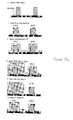
- FIG. 1illustrates cross-section views of a PFET and NFET showing desired stress states.
- FIG. 2illustrates a cross section view of a gate sidewall spacer structure.
- FIG. 3illustrates stress contours induced by an intrinsically tensile spacer for the device outline of FIG. 2.
- FIGS. 4 a - billustrate an exemplary inventive process for fabricating NFETs and PFETs on a common substrate each having stress inducing spacers thereon.
- FIGS. 5 a - gillustrate a third embodiment of the present invention.
- FIG. 6illustrates a simulation of the compressive channel stress in a PFET of the third embodiment.
- FIGS. 7 a - billustrate a fourth embodiment of the present invention.
- FIG. 7 cillustrates a top view of a PFET formed according to the present invention.
- FIG. 8illustrates a simulation of the compressive channel stress in a PFET of the fourth embodiment.
- FIG. 2illustrates a portion of the typical structure of an FET device depicted in FIG. 1.
- the bulk substrate regionis shown in the bottom portion of the Figure, whereas the gate terminal is disposed on the substrate with a very thin oxide layer between it and the substrate.
- the spaceris the dark “L” shaped region adjacent both the substrate and the gate terminal.
- the longitudinal stress contours, indicating stress magnitudeare given in FIG. 3 for the case where the spacer has an intrinsic tensile stress.
- the stress contour lines closer to the substrate top surfacefollow the contours of greater stress magnitude. This creates a tensile stress under the gate as desired.
- the transverse stressis also tensile for the same intrinsic tensile spacer stress, but is much smaller and can be neglected from a stress effect on device characteristic point of view.
- the stress stateswould then reverse as compared to FIG. 3, however, the shape of the stress contours would remain the same.
- the compression needed in the longitudinal direction for the pFETis thus obtained with negligible compressive stresses in the transverse direction.
- nitride filmscan be readily modulated to have very high intrinsic stress ranging from tension to compression.
- PECVDPulsma Enhanced CVD
- nitride etch stop film stresscould be modulated (by changing the deposition conditions such as SiH4/N2/He flow rates, pressure, HF power, and electrode gap) between ⁇ 1.4 GPa and +0.3 GPa.
- LPCVD nitrideshave been known to create tensile stresses up to 10.4 GPa.
- HDP oxideis known to induce compressive stresses while TEOS can impose tension. The following are example conditions that may be used to generate compressive SiN by PECVD.
- Standard parameters for Plasma RF powerare 300 Watts, by increasing the power to 900 W, using a pressure of about 5.75 torr., at 480 C, and a spacing of about 395 mils, a film with compression of about ⁇ 1.6 GPa is achieved.
- Conditions that may be used to generate tensile SiN films by PECVDthe power may be lowered to about 100 W, with the pressure at about 5.75 torr, and temperature of about 480 C to generate a film with about +400 MPa.
- the pressuremay be increased from about from 5.75 torr. to 6.5 torr and the spacing may be increased to 490 mils from about 395 mils at a temperature of about 480 C to generate a film with about 500 MPa.
- the temperaturemay be lowered to 380 C to generate more tension in the film.
- a thermal CVD processmay be used to generate a tensile film of about 1.4 GPa.
- materialsare readily available to pick the correct stress for the spacer film.
- steps 1 - 12 in FIGS. 4 a - bare given by steps 1 - 12 in FIGS. 4 a - b (It is to be noted that the device regions and spacer regions in these figures are not drawn to scale in any dimension):
- steps 1 - 12 in FIGS. 4 a - bare given by steps 1 - 12 in FIGS. 4 a - b (It is to be noted that the device regions and spacer regions in these figures are not drawn to scale in any dimension):
- steps 2using, preferably a low temperature (380-480 C) oxide SiO 2 .
- the next stepinvolves etching the SiN from the NFET ( 5 ); removing the block mask and depositing the conformal etch stop layer again ( 6 ).
- a tensile deposition of SiNfollows ( 7 ), as explained above (for positive stress values, e.g. +500 MPa), then a standard resist block mask is patterned over the NFET ( 8 ).
- the tensile SiNis etched from the PFET ( 9 ) then the block mask is removed and a conformal oxide layer is deposited ( 10 ).
- a SiO 2 spacer etchis then used to shape the oxide spacer remaining on the SiN sidewall ( 11 ).
- Step 12leads to completely symmetric devices because the spacer etch leaves behind the same length of foot for the pFETs and nFETs on each side. Control of the foot length can modulate the stress to some extent.
- each of the conformal oxide layer depositions ( 2 , 6 , 10 )are replaced with a nitride layer deposition, while the deposition of compressive nitride ( 3 ) is replaced with an HDP layer deposition, and the tensile nitride deposition ( 9 ) is replaced with a TEOS layer deposition.
- FIGS. 5 a - gA third embodiment of the present invention is illustrated in FIGS. 5 a - g , wherein a sidewall liner is defined selectively where compressive longitudinal stress is desired.
- FIG. 5 aillustrates a starting structure formed with conventional processing of a standard wafer (SOI in this example). A thermal pad oxide and a deposited pad nitride are formed on the surface of the wafer using methods well known in the art. Next, shown in FIG. 5 b , active areas (trench isolation) are patterned and etched to the BOX. An AA sidewall oxide is grown, and a thin SiN liner is deposited.
- FIG. 5 cshows the next step wherein a thin amorphous or polysilicon layer is conformally deposited. Next, as shown in FIG.
- a bilayer resistis deposited and patterned, however, a single layer resist may be acceptable for shallow topography.
- the exposed Si lineris selectively isotropically etched from those devices, as shown in FIG. 5 e .
- the remaining bilayer resistis stripped, using well known methods.
- the Si lineris then oxidized at low-temperature, to minimize stress relief due to reflow.
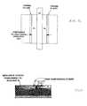
- the volume expansion of the oxidized siliconinduces a bending moment in the SOI island, represented by the upward and inward arrows in the Figure, resulting in a compressive stress at the surface of the SOI (where the device channel will be subsequently formed).
- Liner thicknesscan be varied to tune the magnitude of the stress.
- materials other than poly or amorphous siliconcan be used for the liner, such as germanium doped silicon or silicon nitride.
- deposition of an isolation material and planarization, which follows this oxidation step as described below,can precede the oxidation step.
- FIG. 6shows the stress regions, indicated by shading, imposed on the SOI regions and in the Box layer, demonstrating the generation of a strong longitudinal compressive stress in the channel of the pMOSFET due to volume expansion of the oxidized poly spacers. The stress is well confined to the device of interest.
- the SOI thickness in this exampleis approximately 80 nm.
- An alternative final stepinvolves subjecting the silicon liner to a RIE etch to form spacers which are subsequently oxidized.
- This alternative processachieves similar bending moments in the SOI as illustrated in FIG. 5 g .
- Normally practiced processingfollows the structures of FIGS. 5 f and 5 g , which includes STI fill and planarization down to the SOI top surface, body doping implants, gate dielectric formation, gate conductor formation, source-drain implants, contacts, and various higher levels of metallurgy and interlayer dielectrics.
- FIGS. 7 a - billustrate a fourth embodiment of the present invention, continuing from the previously described process at the step shown in FIG. 5 e .
- This fourth embodimentcomprises oxidation of the etched silicon liner (or spacer) after STI fill and planarization.
- the resist layersare stripped and the isolation regions are filled with oxide and planarized by well known conventional methods, resulting in the structure shown in FIG. 7 a .
- the oxide fillpreferably comprises TEOS to facilitate diffusion of oxygen to the silicon liner.
- the remaining polysilicon liner regionsare oxidized through the STI, creating a compressive stress in the SOI island, as illustrate by the inwardly pointing arrows in FIG. 7 b .
- FIG. 7 cshows a top view of the PFET, fabricated according to the methods just described, containing the oxidized liner, with the gate conductor (GC) over the channel region that is disposed between the diffusions (P+), and showing the direction of imposed longitudinal stress propagating through the channel region.
- FIG. 8illustrates the compressive stress patterns in this embodiment showing that a large compressive stress is created in the SOI island in the direction of channel current.
- the peak compressive stressoccurs near the top of the SOI layer adjacent the oxidized polysilicon.
- the lighter shades extending away from the peak compression regionsindicate regions of dissipating stress. As can be seen in this figure, negligible propagation of stress to adjacent SOI island occurs.
- the SOI thicknessis about 80 nm.
- One embodiment of the present inventioninvolves forming spacers with different intrinsically stress inducing materials to impart selected longitudinal stress components upon active device regions formed in a substrate, in one embodiment.
- a stress inducing material that is intrinsically tensilecauses a tensile state of stress in a desired substrate channel region and an intrinsically compressive material causes compression in the same substrate channel region.
- deposited filmsthat impose different intrinsic stresses.
- TEOSis tensile while HDP (high density plasma) is compressive.
- the key hereis to integrate two different intrinsically stress inducing spacers adjacent the gates of the NFETs and PFETs or individually.
- the present solutionshows how to apply the correct states of stress through modifying the sidewall spacer process to benefit both the NFET and PFET simultaneously. It also differs substantially from both of these other approaches since the tension and compression are achieved through spacer structures that are physically close to the affected device regions whereas the prior art listed above shows the stress is imposed through strained Si in one case and from intrinsic stress in a layer that comes well after the device build (and not adjacent the device as we do).
- the advantages of the method of the preferred embodiment of this inventioninclude: device performance improvements for NFETs, PFETs, and for both NFETs and PFETs simultaneously; a process readily integratible into present manufacturing processes for bulk silicon, silicon-on-insulator (“SOI”), and strained silicon structures; and improved devices be integrated into present processes cheaply for significant device performance improvements.
- SOIsilicon-on-insulator
- spacer materialscan be used, such as ceramics and silicon carbide, which can also impart intrinsic stresses.
- the general view of stresses in siliconis that it's disadvantageous. Stresses lead to ruptures or dislocations in the lattice structure, which lead to junction leakage, etc. In the present invention, we're intentionally building in a stress pattern.
Landscapes
- Thin Film Transistor (AREA)
- Metal-Oxide And Bipolar Metal-Oxide Semiconductor Integrated Circuits (AREA)
- Element Separation (AREA)
- Insulated Gate Type Field-Effect Transistor (AREA)
Abstract
Description
- U.S. patent application Ser. No. ______, entitled “Isolation Structures for Imposing Stress Patterns” filed concurrently herewith is assigned to the same assignee hereof and contains subject matter related, in certain respect, to the subject matter of the present application. The above-identified patent application is incorporated herein by reference.[0001]
- 1. Technical Field of the Invention[0002]
- This invention pertains to inventive methods of manufacturing a semiconductor device for improving device performance, and to the resulting unique high-performance device structure. In particular, this invention has improved charge mobility in FET devices by structurally imposing tensile and compression forces in a device substrate during device fabrication.[0003]
- Within the field of semiconductor device design, it is known that mechanical stresses within the device substrate can modulate device performance. Individual stress tensor components affect device behavior of PFETs and NFETs differently. Previous improvements that utilized stress enhancements tended to focus on one or the other type of device outside of a practical performance environment, such as in an IC chip. In order to maximize the performance of both PFETs and NFETs within IC chips, the stress components need to be engineered and applied differently, yet simultaneously. The best stress design is tension in both directions for the nFET and compression in the longitudinal direction for the pFET along with tension in the transverse direction relative to channel current. In this invention we show a method and structure by which we can use spacers to introduce a longitudinal tensile stress for the nFET while at the same time applying a longitudinal compressive stress on the pFET device in a conventional FET structure, and selectively deposited layers on silicon-on-insulator (“SOI”) structures. The longitudinal stress is induced along the same axis as the current, or charge, being carried in the channel. It may be more difficult to impose a stress in the transverse direction using spacers so we lose benefit from that direction. However, by virtue of the fact that we can move the stress inducing component closer to the device through the use of stress inducing spacers and layers, the modulation of stress can be improved relative to the isolation material or STI stress approach as suggested in the patent application identified above. One advantage of the method and structure of the present invention that it has provided a device performance improvement for both the nFET and pFET simultaneously.[0004]
- 2. Description of the Prior Art[0005]
- Ito et al (IEDM, 2000) impose stress using an etch-stop nitride superlayer that is deposited after the device is completely constructed. Again, here the films have a built-in intrinsic biaxial stress which they modulated from compressive through tensile. They found that when the film is in tension the nFET performance is enhanced while that of the pFET's is degraded. They found the reverse for compression, namely NFET is degraded while the pFET is enhanced. They could not improve the performance of both the pFET and nFET simultaneously. Also, since the film is well above the device the stress translated down into the silicon will be somewhat lesser, particularly when compared to material that is adjacent to the device.[0006]
- In the application identified above entitled “Isolation Structures for Imposing Stress Patterns”, we showed how to modulate the stresses imposed on the silicon by isolation (the preferred example used STI). One of the embodiments advocates the use of materials with different intrinsic stress and coefficients of expansion mismatched in the appropriate regions of the nFETs and pFETs to modulate induced stresses. In another embodiment, we discussed how to add compressive stress by oxidation through openings in a nitride liner as needed for pFETs in the longitudinal direction, while retaining all the tensile stresses (in the transverse pFET direction and transverse+longitudinal nFET directions) from intrinsic and thermal mismatch properties. Prior to these two recent disclosures, all prior known solutions and methods using mechanical stress for device performance enhancement improved neither both nFETs and pFETs simultaneously nor taught the individual device isolation structures and methods of making them. In the present specification we leverage stress effects on devices using stress induced by spacers and by processing, e.g. oxidizing, a selectively deposited silicon isolation liner on SOI structures. We also show how to modulate the stresses for both pFETs and nFETs, which brings the stress effect much closer to the device.[0007]
- In this invention we show methods and structures by which we have applied tensile stress for the NFET while at the same time applying a compressive longitudinal stress on the PFET device. The structures and methods of making each device individually is also unique. Other disclosed embodiments teach structures, and methods of formation, for selectively inducing strain in the channel of pMOSFETs by using a patterned and oxidized isolation liner. Particular embodiments of the present invention rely upon the volume expansion of a patterned and oxidized silicon liner in isolation regions, or spacers on gate sidewalls, to selectively induce appropriate strain in the channels of adjacent pMOSFETs. The oxidized silicon liner induces a bending moment in an SOI island, resulting in a compressive stress centered in the channel. The compressive stress on the longitudinal component of the PFET may be tuned by varying the thickness of the silicon liner or, in another embodiment, structures and methods of formation are illustrated by which patterned and oxidized spacers on the sidewalls of the active area are used to introduce a longitudinal compressive stress on the pFET device. Through the use of patterned oxidized spacers, the stress is applied closer to the device than is possible with STI fill alone, significantly improving the ability to modulate the stress. It is also shown that the structure of the invention has a negligible effect on stress induced on adjacent devices, where stress modification may not be desired.[0008]
- The primary advantage of these methods and structures is that they have provided device performance improvement. Another advantage is the method for fabricating NFETs and PFETs simultaneously on a common substrate, wherein each device is designed to enhance performance using stress inducing spacers and isolation liners. A secondary advantage is the structure and method of building an individual device with enhanced performance provided via stress inducing spacers and liners.[0009]
- It is an object of the present invention to provide device performance improvements for NFETs, PFETs, and for both NFETs and PFETs simultaneously. It is another object of the present invention to be readily integratible into present manufacturing processes. It is another object of the present invention to be manufacturable in bulk silicon, silicon-on-insulator (“SOI”), and strained silicon structures. It is yet another object of the present invention to provide improved devices that can be integrated into present processes cheaply for significant device performance improvements.[0010]
- This invention comprises a spacer structure for an NFET device and for a PFET device. A spacer region for the NFET device contains therein a first spacer material which applies a first type of mechanical stress on the NFET device in a longitudinal direction. A spacer region for the PFET device applies an opposing mechanical stress on the PFET device in the same longitudinal direction. The spacer regions may comprise similar or different spacer materials. Typically, the mechanical stresses are either tensile or compressive.[0011]
- In another aspect, this invention comprises a method for making NFET and PFET devices. This aspect incorporates the formation of spacer regions at the sidewalls of the NFET gate. Another spacer is formed on the sidewalls of the PFET gate. Spacer materials in these spacer regions are selected to apply a first type of mechanical stress on the NFET device in the longitudinal direction (same axis as the direction of the device's channel current) and another type of mechanical stress on the PFET device in the longitudinal direction.[0012]
- In another aspect, the present invention comprises source and drain regions formed in a substrate. The substrate having a channel region between each of the source and drain regions. A gate region adjacent the channel region controls conduction through the channel region. Stress inducing spacer material adjacent selected sides of the gate region imparts stress, i.e. tension or compression, to at least the channel region of the substrate.[0013]
- In another aspect, this invention comprises an IC chip comprising, and a method of making on the IC chip, a plurality of stressed SOI regions and a plurality of unstressed SOI regions for use in FET and/or device manufacturing. FET devices on the IC chip comprise a stress inducing layer only on the ends of the stressed SOI regions. The stress inducing layer is deposited as a separate IC fabrication step. This stress inducing layer is then exposed to a preselected agent, which may be, for example, a gas, that modifies, e.g. expands, the stress inducing layer which then propagates a longitudinal mechanical stress in the SOI regions.[0014]
- Other features and advantages of this invention will become apparent from the following detailed description of the presently preferred embodiment of the invention, taken in conjunction with the accompanying drawings.[0015]
- FIG. 1 illustrates cross-section views of a PFET and NFET showing desired stress states.[0016]
- FIG. 2 illustrates a cross section view of a gate sidewall spacer structure.[0017]
- FIG. 3 illustrates stress contours induced by an intrinsically tensile spacer for the device outline of FIG. 2.[0018]
- FIGS. 4[0019]a-billustrate an exemplary inventive process for fabricating NFETs and PFETs on a common substrate each having stress inducing spacers thereon.
- FIGS. 5[0020]a-gillustrate a third embodiment of the present invention.
- FIG. 6 illustrates a simulation of the compressive channel stress in a PFET of the third embodiment.[0021]
- FIGS. 7[0022]a-billustrate a fourth embodiment of the present invention.
- FIG. 7[0023]cillustrates a top view of a PFET formed according to the present invention.
- FIG. 8 illustrates a simulation of the compressive channel stress in a PFET of the fourth embodiment.[0024]
- As shown in FIG. 1 below, wherein “C” indicates induced compression stresses in the substrate and “T” indicates induced tension stresses in the substrate, we wish to apply a longitudinal (in direction of channel current) tensile stress in the channel region under the gate for the nFET while applying a longitudinal compressive stress in the same region for the PFET. Stress inducing spacers are used, wherein the outward arrows from the gate sidewall on the NFET shows tensile spacer material, while the device body areas affected by the spacer material is labeled according to the induced stress effected there. Opposite effects are as shown in the PFET. We need to use spacers of the same intrinsic stress as is needed in the channel under the gate. While the induced stress would be relatively non-uniform and the length scale of their effects on the order of 3× the spacer thickness, since the spacer is now very close to the device, we expect the stress effect to play a significant role in device modulation. The key here is the process that allows two different spacers, one for the PFET and one for the NFET.[0025]
- FIG. 2 illustrates a portion of the typical structure of an FET device depicted in FIG. 1. The bulk substrate region is shown in the bottom portion of the Figure, whereas the gate terminal is disposed on the substrate with a very thin oxide layer between it and the substrate. The spacer is the dark “L” shaped region adjacent both the substrate and the gate terminal. For the NFET device structure shown in FIG. 2, the longitudinal stress contours, indicating stress magnitude are given in FIG. 3 for the case where the spacer has an intrinsic tensile stress. The stress contour lines closer to the substrate top surface follow the contours of greater stress magnitude. This creates a tensile stress under the gate as desired. The transverse stress is also tensile for the same intrinsic tensile spacer stress, but is much smaller and can be neglected from a stress effect on device characteristic point of view. For the case of the pFET when a spacer with intrinsically compressive stress is used the stress states would then reverse as compared to FIG. 3, however, the shape of the stress contours would remain the same. The compression needed in the longitudinal direction for the pFET is thus obtained with negligible compressive stresses in the transverse direction.[0026]
- Before we get into a deeper description of the process and structure, we first examine the possible spacer materials for the nFET and pFET respectively. For instance nitride films can be readily modulated to have very high intrinsic stress ranging from tension to compression. For example, as shown in Ito et al (IEDM, 2000) the PECVD (Plasma Enhanced CVD) nitride etch stop film stress could be modulated (by changing the deposition conditions such as SiH4/N2/He flow rates, pressure, HF power, and electrode gap) between −1.4 GPa and +0.3 GPa. We have been able to replicate these stresses in our nitrides by modulating deposition conditions and have been able to create −1.4 GPa to +0.4 GPa intrinsic stresses in the nitride, as measured with wafer curvature techniques. LPCVD nitrides have been known to create tensile stresses up to 10.4 GPa. HDP oxide is known to induce compressive stresses while TEOS can impose tension. The following are example conditions that may be used to generate compressive SiN by PECVD. Standard parameters for Plasma RF power are 300 Watts, by increasing the power to 900 W, using a pressure of about 5.75 torr., at 480 C, and a spacing of about 395 mils, a film with compression of about −1.6 GPa is achieved. Conditions that may be used to generate tensile SiN films by PECVD: the power may be lowered to about 100 W, with the pressure at about 5.75 torr, and temperature of about 480 C to generate a film with about +400 MPa. The pressure may be increased from about from 5.75 torr. to 6.5 torr and the spacing may be increased to 490 mils from about 395 mils at a temperature of about 480 C to generate a film with about 500 MPa. The temperature may be lowered to 380 C to generate more tension in the film. Alternatively, a thermal CVD process may be used to generate a tensile film of about 1.4 GPa. Thus, materials are readily available to pick the correct stress for the spacer film.[0027]
- One example of the process steps by which we get the two separate and distinctly differently stressed spacers on the nFET and pFET, particularly from an intrinsic stress viewpoint, are given by steps[0028]1-12 in FIGS. 4a-b(It is to be noted that the device regions and spacer regions in these figures are not drawn to scale in any dimension): Starting with conventional gate stack formation for both PFET and NFET (1), we applied conformal etch stop material over exposed surfaces (2) using, preferably a low temperature (380-480 C) oxide SiO2. Next is a deposition of compressive SiN (3), as explained above (for negative stress values, e.g. −1.6 GPa), and a standard resist block mask over the PFET (4). The next step involves etching the SiN from the NFET (5); removing the block mask and depositing the conformal etch stop layer again (6). A tensile deposition of SiN follows (7), as explained above (for positive stress values, e.g. +500 MPa), then a standard resist block mask is patterned over the NFET (8). The tensile SiN is etched from the PFET (9) then the block mask is removed and a conformal oxide layer is deposited (10). A SiO2spacer etch is then used to shape the oxide spacer remaining on the SiN sidewall (11). Finally, a SiN etch forms the stress inducing spacers as illustrated in
step 12.Step 12 leads to completely symmetric devices because the spacer etch leaves behind the same length of foot for the pFETs and nFETs on each side. Control of the foot length can modulate the stress to some extent. - Another embodiment of the present invention can be implemented using the process described above except that the known stress inducing materials HDP and TEOS are used. In this second embodiment, each of the conformal oxide layer depositions ([0029]2,6,10) are replaced with a nitride layer deposition, while the deposition of compressive nitride (3) is replaced with an HDP layer deposition, and the tensile nitride deposition (9) is replaced with a TEOS layer deposition.
- A third embodiment of the present invention is illustrated in FIGS. 5[0030]a-g, wherein a sidewall liner is defined selectively where compressive longitudinal stress is desired. FIG. 5aillustrates a starting structure formed with conventional processing of a standard wafer (SOI in this example). A thermal pad oxide and a deposited pad nitride are formed on the surface of the wafer using methods well known in the art. Next, shown in FIG. 5b, active areas (trench isolation) are patterned and etched to the BOX. An AA sidewall oxide is grown, and a thin SiN liner is deposited. FIG. 5cshows the next step wherein a thin amorphous or polysilicon layer is conformally deposited. Next, as shown in FIG. 5d, a bilayer resist is deposited and patterned, however, a single layer resist may be acceptable for shallow topography. Wherever enhanced stress is not desired, the exposed Si liner is selectively isotropically etched from those devices, as shown in FIG. 5e. Finally, as shown in FIG. 5f, the remaining bilayer resist is stripped, using well known methods. The Si liner is then oxidized at low-temperature, to minimize stress relief due to reflow. The volume expansion of the oxidized silicon induces a bending moment in the SOI island, represented by the upward and inward arrows in the Figure, resulting in a compressive stress at the surface of the SOI (where the device channel will be subsequently formed). Liner thickness can be varied to tune the magnitude of the stress. Alternatively, materials other than poly or amorphous silicon can be used for the liner, such as germanium doped silicon or silicon nitride. Also, deposition of an isolation material and planarization, which follows this oxidation step as described below, can precede the oxidation step. FIG. 6 shows the stress regions, indicated by shading, imposed on the SOI regions and in the Box layer, demonstrating the generation of a strong longitudinal compressive stress in the channel of the pMOSFET due to volume expansion of the oxidized poly spacers. The stress is well confined to the device of interest. The SOI thickness in this example is approximately 80 nm.
- An alternative final step involves subjecting the silicon liner to a RIE etch to form spacers which are subsequently oxidized. This alternative process achieves similar bending moments in the SOI as illustrated in FIG. 5[0031]g. Normally practiced processing follows the structures of FIGS. 5fand5g, which includes STI fill and planarization down to the SOI top surface, body doping implants, gate dielectric formation, gate conductor formation, source-drain implants, contacts, and various higher levels of metallurgy and interlayer dielectrics. These further processing steps are not considered part of the present invention and are not discussed further.
- FIGS. 7[0032]a-billustrate a fourth embodiment of the present invention, continuing from the previously described process at the step shown in FIG. 5e. This fourth embodiment comprises oxidation of the etched silicon liner (or spacer) after STI fill and planarization. Beginning with the structure shown in FIG. 5e, the resist layers are stripped and the isolation regions are filled with oxide and planarized by well known conventional methods, resulting in the structure shown in FIG. 7a. The oxide fill preferably comprises TEOS to facilitate diffusion of oxygen to the silicon liner. The remaining polysilicon liner regions are oxidized through the STI, creating a compressive stress in the SOI island, as illustrate by the inwardly pointing arrows in FIG. 7b. Various oxidation conditions, STI fill composition, and liner thickness can be employed to tune the magnitude of the stress. Alternatively, materials other than poly or amorphous silicon can be used for the liner, such as germanium doped silicon or silicon nitride. Standard processing continues from this point to completion of the chip. FIG. 7cshows a top view of the PFET, fabricated according to the methods just described, containing the oxidized liner, with the gate conductor (GC) over the channel region that is disposed between the diffusions (P+), and showing the direction of imposed longitudinal stress propagating through the channel region. FIG. 8 illustrates the compressive stress patterns in this embodiment showing that a large compressive stress is created in the SOI island in the direction of channel current. The peak compressive stress occurs near the top of the SOI layer adjacent the oxidized polysilicon. The lighter shades extending away from the peak compression regions indicate regions of dissipating stress. As can be seen in this figure, negligible propagation of stress to adjacent SOI island occurs. The SOI thickness is about 80 nm.
- One embodiment of the present invention involves forming spacers with different intrinsically stress inducing materials to impart selected longitudinal stress components upon active device regions formed in a substrate, in one embodiment. For example, using a stress inducing material that is intrinsically tensile causes a tensile state of stress in a desired substrate channel region and an intrinsically compressive material causes compression in the same substrate channel region. In order to impart these different stresses in devices, we use deposited films that impose different intrinsic stresses. For example, TEOS is tensile while HDP (high density plasma) is compressive. The key here is to integrate two different intrinsically stress inducing spacers adjacent the gates of the NFETs and PFETs or individually.[0033]
- In the prior art, Rim et. al. apply biaxial tension in strained silicon using a SiGe relaxed sub-layer. The problems there are many. While the NFET shows what may be considered significant improvement, they could not simultaneously improve both devices. Also, since the requirement is a relaxed SiGe layer, misfit dislocations are needed at the SiGe/Si interface. One of the major mechanisms by which the misfit dislocations are formed is from threading dislocations. Unfortunately, the threading dislocations can cause significant reliability, yield, and major leakage issues and are difficult to remove in practice.[0034]
- Mechanical Stress affect of Etch-Stop Nitride and its Impact on Deep Submicron Transistor Design, Ito et al (IEDM, 2000) impose stress using an etch-stop nitride superlayer that is deposited after the device is completely constructed. Again, here the films have a built-in intrinsic biaxial stress. They found that when the film is in compression NFET performance is degraded, while the PFET is enhanced. Also, they did not improve the performance of both the PFET and NFET simultaneously. Also, since the film is well above the device the stress translated down into the silicon will be somewhat lessened, particularly when compared to something that is directly adjacent the device.[0035]
- The present solution shows how to apply the correct states of stress through modifying the sidewall spacer process to benefit both the NFET and PFET simultaneously. It also differs substantially from both of these other approaches since the tension and compression are achieved through spacer structures that are physically close to the affected device regions whereas the prior art listed above shows the stress is imposed through strained Si in one case and from intrinsic stress in a layer that comes well after the device build (and not adjacent the device as we do).[0036]
- The advantages of the method of the preferred embodiment of this invention include: device performance improvements for NFETs, PFETs, and for both NFETs and PFETs simultaneously; a process readily integratible into present manufacturing processes for bulk silicon, silicon-on-insulator (“SOI”), and strained silicon structures; and improved devices be integrated into present processes cheaply for significant device performance improvements.[0037]
- It will be appreciated that, although specific embodiments of the invention have been described herein for purposes of illustration, various modifications may be made without departing from the spirit and scope of the invention. In particular, while nitride is a good material choice for the two spacers because the intrinsic stress can be controlled from tension to compression. While this above embodiment with nitride spacers is preferred, this approach is not restricted in material choice. One can have additional options in terms of the material set. HDP can be used for compressive stress while TEOS can be used for tension. The integration of these material choices causes changes in process flow.[0038]
- Other spacer materials can be used, such as ceramics and silicon carbide, which can also impart intrinsic stresses. The general view of stresses in silicon is that it's disadvantageous. Stresses lead to ruptures or dislocations in the lattice structure, which lead to junction leakage, etc. In the present invention, we're intentionally building in a stress pattern.[0039]
- Accordingly, the scope of protection of this invention is limited only by the following claims and their equivalents.[0040]
Claims (20)
Priority Applications (5)
| Application Number | Priority Date | Filing Date | Title |
|---|---|---|---|
| US10/318,602US6825529B2 (en) | 2002-12-12 | 2002-12-12 | Stress inducing spacers |
| TW092133680ATWI230463B (en) | 2002-12-12 | 2003-12-01 | Stress inducing spacers |
| CNB2003101213327ACN1306585C (en) | 2002-12-12 | 2003-12-11 | Stress-introducing spacer layer and manufacturing method thereof |
| CNB200610082638XACN100481468C (en) | 2002-12-12 | 2003-12-11 | Stress inducing spacers |
| US10/935,136US7374987B2 (en) | 2002-12-12 | 2004-09-07 | Stress inducing spacers |
Applications Claiming Priority (1)
| Application Number | Priority Date | Filing Date | Title |
|---|---|---|---|
| US10/318,602US6825529B2 (en) | 2002-12-12 | 2002-12-12 | Stress inducing spacers |
Related Child Applications (1)
| Application Number | Title | Priority Date | Filing Date |
|---|---|---|---|
| US10/935,136DivisionUS7374987B2 (en) | 2002-12-12 | 2004-09-07 | Stress inducing spacers |
Publications (2)
| Publication Number | Publication Date |
|---|---|
| US20040113217A1true US20040113217A1 (en) | 2004-06-17 |
| US6825529B2 US6825529B2 (en) | 2004-11-30 |
Family
ID=32506403
Family Applications (2)
| Application Number | Title | Priority Date | Filing Date |
|---|---|---|---|
| US10/318,602Expired - LifetimeUS6825529B2 (en) | 2002-12-12 | 2002-12-12 | Stress inducing spacers |
| US10/935,136Expired - LifetimeUS7374987B2 (en) | 2002-12-12 | 2004-09-07 | Stress inducing spacers |
Family Applications After (1)
| Application Number | Title | Priority Date | Filing Date |
|---|---|---|---|
| US10/935,136Expired - LifetimeUS7374987B2 (en) | 2002-12-12 | 2004-09-07 | Stress inducing spacers |
Country Status (3)
| Country | Link |
|---|---|
| US (2) | US6825529B2 (en) |
| CN (2) | CN100481468C (en) |
| TW (1) | TWI230463B (en) |
Cited By (57)
| Publication number | Priority date | Publication date | Assignee | Title |
|---|---|---|---|---|
| US20050093078A1 (en)* | 2003-10-30 | 2005-05-05 | Victor Chan | Increasing carrier mobility in NFET and PFET transistors on a common wafer |
| US20050269561A1 (en)* | 2004-06-03 | 2005-12-08 | Dureseti Chidambarrao | Strained Si on multiple materials for bulk or SOI substrates |
| US20050285192A1 (en)* | 2004-06-29 | 2005-12-29 | International Business Machines Corporation | Structures and methods for manufacturing p-type mosfet withgraded embedded silicon-germanium source-drain and/or extension |
| US20060003597A1 (en)* | 2004-06-30 | 2006-01-05 | Oleg Golonzka | Enhanced nitride layers for metal oxide semiconductors |
| US20060060856A1 (en)* | 2004-09-20 | 2006-03-23 | International Business Machines Corporation | High-mobility bulk silicon pfet |
| WO2006049834A1 (en)* | 2004-10-29 | 2006-05-11 | Advanced Micro Devices, Inc. | A semiconductor device including semiconductor regions having differently strained channel regions and a method of manufacturing the same |
| US20060113568A1 (en)* | 2004-11-30 | 2006-06-01 | International Business Machines Corporation | Structure and method of applying stresses to pfet and nfet transistor channels for improved performance |
| US20060228848A1 (en)* | 2005-03-31 | 2006-10-12 | International Business Machines Corporation | Dual-hybrid liner formation without exposing silicide layer to photoresist stripping chemicals |
| US7122849B2 (en) | 2003-11-14 | 2006-10-17 | International Business Machines Corporation | Stressed semiconductor device structures having granular semiconductor material |
| US20060246672A1 (en)* | 2005-04-29 | 2006-11-02 | Chien-Hao Chen | Method of forming a locally strained transistor |
| US20060244074A1 (en)* | 2005-04-29 | 2006-11-02 | Chien-Hao Chen | Hybrid-strained sidewall spacer for CMOS process |
| US20060249794A1 (en)* | 2005-05-04 | 2006-11-09 | Chartered Semiconductor Manufacturing, Ltd | Method to remove spacer after salicidation to enhance contact etch stop liner stress on MOS |
| US20060252194A1 (en)* | 2005-05-04 | 2006-11-09 | Chartered Semiconductor Manufacturing Ltd. | Composite stress spacer |
| US20060255415A1 (en)* | 2005-05-12 | 2006-11-16 | International Business Machines Corporation | Structure and method of making a field effect transistor having an asymmetrically stressed channel region |
| US20060269693A1 (en)* | 2005-05-26 | 2006-11-30 | Applied Materials, Inc. | Method to increase tensile stress of silicon nitride films using a post PECVD deposition UV cure |
| US20060270217A1 (en)* | 2005-05-26 | 2006-11-30 | Applied Materials, Inc. | Integration process for fabricating stressed transistor structure |
| US20060289900A1 (en)* | 2005-06-23 | 2006-12-28 | Applied Materials, Inc. | Methods for forming a transistor and creating channel stress |
| US20070001217A1 (en)* | 2005-06-29 | 2007-01-04 | Shang-Chih Chen | Closed loop CESL high performance CMOS devices |
| US20070001233A1 (en)* | 2005-06-30 | 2007-01-04 | Christoph Schwan | Technique for forming contact insulation layers and silicide regions with different characteristics |
| WO2007005136A1 (en)* | 2005-06-30 | 2007-01-11 | Advanced Micro Devices, Inc. | Technique for forming contact insulation layers silicide regions with different characteristics |
| US20070034940A1 (en)* | 2005-08-12 | 2007-02-15 | Kabushiki Kaisha Toshiba | MOS semiconductor device |
| US20070096170A1 (en)* | 2005-11-02 | 2007-05-03 | International Business Machines Corporation | Low modulus spacers for channel stress enhancement |
| US20070111421A1 (en)* | 2004-12-15 | 2007-05-17 | International Business Machines Corporation | Structure and method to generate local mechanical gate stress for mosfet channel mobility modification |
| US20070122965A1 (en)* | 2005-09-29 | 2007-05-31 | International Business Machines Corporation | Stress engineering using dual pad nitride with selective soi device architecture |
| DE102005057073A1 (en)* | 2005-11-30 | 2007-05-31 | Advanced Micro Devices, Inc., Sunnyvale | Forming semiconductor component comprises forming metal silicide on two transistors while other is masked and then forming contact layers of given internal tension |
| US20070145430A1 (en)* | 2005-12-22 | 2007-06-28 | Micron Technology, Inc. | CMOS device with asymmetric gate strain |
| US20070252230A1 (en)* | 2006-04-28 | 2007-11-01 | International Business Machines Corporation | Cmos structures and methods for improving yield |
| US20070254422A1 (en)* | 2006-04-28 | 2007-11-01 | International Business Machines Corporation | High performance stress-enhance mosfet and method of manufacture |
| US20070254423A1 (en)* | 2006-04-28 | 2007-11-01 | International Business Machines Corporation | High performance stress-enhance mosfet and method of manufacture |
| US20070269992A1 (en)* | 2006-05-19 | 2007-11-22 | International Business Machines Corporation | Compressive nitride film and method of manufacturing thereof |
| US7314802B2 (en) | 2005-02-15 | 2008-01-01 | International Business Machines Corporation | Structure and method for manufacturing strained FINFET |
| US20080020591A1 (en)* | 2005-05-26 | 2008-01-24 | Applied Materials, Inc. | Method to increase silicon nitride tensile stress using nitrogen plasma in-situ treatment and ex-situ uv cure |
| US20080057673A1 (en)* | 2006-08-30 | 2008-03-06 | International Business Machines Corporation | Semiconductor structure and method of making same |
| US20080057653A1 (en)* | 2006-08-30 | 2008-03-06 | International Business Machines Corporation | Method and structure for improving device performance variation in dual stress liner technology |
| GB2442174A (en)* | 2005-06-30 | 2008-03-26 | Advanced Micro Devices Inc | Technique for forming contact insulation layers silicide regions with different characteristics |
| US20080128765A1 (en)* | 2004-12-15 | 2008-06-05 | Chien-Hao Chen | MOSFET Device With Localized Stressor |
| US20080128831A1 (en)* | 2005-11-16 | 2008-06-05 | United Microelectronics Corp. | Cmos and mos device |
| US20080191287A1 (en)* | 2007-02-13 | 2008-08-14 | Pei-Yu Chou | Method for fabricating strained-silicon cmos transistor |
| US20080237733A1 (en)* | 2007-03-27 | 2008-10-02 | International Business Machines Corporation | Structure and method to enhance channel stress by using optimized sti stress and nitride capping layer stress |
| US20080272404A1 (en)* | 2007-05-04 | 2008-11-06 | Dsm Solutions, Inc. | Method for applying a stress layer to a semiconductor device and device formed therefrom |
| US20090127626A1 (en)* | 2007-11-15 | 2009-05-21 | International Business Machines Corporation | Stress-generating shallow trench isolation structure having dual composition |
| US20090305474A1 (en)* | 2004-06-24 | 2009-12-10 | International Business Machines Corporation | Strained-silicon cmos device and method |
| US20090305471A1 (en)* | 2006-01-11 | 2009-12-10 | International Business Machines Corporation | Thin silicon single diffusion field effect transistor for enhanced drive performance with stress film liners |
| US7790540B2 (en) | 2006-08-25 | 2010-09-07 | International Business Machines Corporation | Structure and method to use low k stress liner to reduce parasitic capacitance |
| US20100308381A1 (en)* | 2009-06-08 | 2010-12-09 | Globalfoundries Inc. | Finfet structures with stress-inducing source/drain-forming spacers and methods for fabricating the same |
| US7935993B2 (en) | 2006-01-10 | 2011-05-03 | International Business Machines Corporation | Semiconductor device structure having enhanced performance FET device |
| US7960801B2 (en) | 2005-11-03 | 2011-06-14 | International Business Machines Corporation | Gate electrode stress control for finFET performance enhancement description |
| US20110230030A1 (en)* | 2010-03-16 | 2011-09-22 | International Business Machines Corporation | Strain-preserving ion implantation methods |
| US8058157B2 (en) | 2005-11-30 | 2011-11-15 | International Business Machines Corporation | FinFET structure with multiply stressed gate electrode |
| EP2235744A4 (en)* | 2008-01-22 | 2011-12-14 | Ibm | ANISOTROPIC STRAIN GENERATION BY STRAIN GENERATING COATINGS HAVING A SUBLITHOGRAPHIC WIDTH |
| US8115254B2 (en) | 2007-09-25 | 2012-02-14 | International Business Machines Corporation | Semiconductor-on-insulator structures including a trench containing an insulator stressor plug and method of fabricating same |
| US20120083106A1 (en)* | 2010-09-30 | 2012-04-05 | Institute of Microelectronics, Chinese Academy of Sciences | Method for manufacturing semiconductor structure |
| US8853746B2 (en) | 2006-06-29 | 2014-10-07 | International Business Machines Corporation | CMOS devices with stressed channel regions, and methods for fabricating the same |
| US9018108B2 (en) | 2013-01-25 | 2015-04-28 | Applied Materials, Inc. | Low shrinkage dielectric films |
| US9240351B2 (en) | 2009-12-31 | 2016-01-19 | Institute of Microelectronics, Chinese Academy of Sciences | Field effect transistor device with improved carrier mobility and method of manufacturing the same |
| US20190378927A1 (en)* | 2018-06-12 | 2019-12-12 | Taiwan Semiconductor Manufacturing Company Ltd. | Semiconductor device and method for forming the same |
| US20210313467A1 (en)* | 2002-11-20 | 2021-10-07 | Renesas Electronics Corporation | Semiconductor device including gate electrode for applying tensile stress to silicon substrate, and method of manufacturing the same |
Families Citing this family (107)
| Publication number | Priority date | Publication date | Assignee | Title |
|---|---|---|---|---|
| CN1449585A (en)* | 2000-11-22 | 2003-10-15 | 株式会社日立制作所 | Semiconductor device and manufacturing method thereof |
| JP2002232075A (en)* | 2001-01-31 | 2002-08-16 | Ando Electric Co Ltd | Tunable light source |
| US7001837B2 (en)* | 2003-01-17 | 2006-02-21 | Advanced Micro Devices, Inc. | Semiconductor with tensile strained substrate and method of making the same |
| US6870179B2 (en)* | 2003-03-31 | 2005-03-22 | Intel Corporation | Increasing stress-enhanced drive current in a MOS transistor |
| US7279746B2 (en)* | 2003-06-30 | 2007-10-09 | International Business Machines Corporation | High performance CMOS device structures and method of manufacture |
| US7410846B2 (en)* | 2003-09-09 | 2008-08-12 | International Business Machines Corporation | Method for reduced N+ diffusion in strained Si on SiGe substrate |
| US6887751B2 (en) | 2003-09-12 | 2005-05-03 | International Business Machines Corporation | MOSFET performance improvement using deformation in SOI structure |
| US6872641B1 (en)* | 2003-09-23 | 2005-03-29 | International Business Machines Corporation | Strained silicon on relaxed sige film with uniform misfit dislocation density |
| US7144767B2 (en)* | 2003-09-23 | 2006-12-05 | International Business Machines Corporation | NFETs using gate induced stress modulation |
| US7119403B2 (en) | 2003-10-16 | 2006-10-10 | International Business Machines Corporation | High performance strained CMOS devices |
| US7303949B2 (en) | 2003-10-20 | 2007-12-04 | International Business Machines Corporation | High performance stress-enhanced MOSFETs using Si:C and SiGe epitaxial source/drain and method of manufacture |
| US7037770B2 (en) | 2003-10-20 | 2006-05-02 | International Business Machines Corporation | Method of manufacturing strained dislocation-free channels for CMOS |
| US8008724B2 (en)* | 2003-10-30 | 2011-08-30 | International Business Machines Corporation | Structure and method to enhance both nFET and pFET performance using different kinds of stressed layers |
| US7129126B2 (en) | 2003-11-05 | 2006-10-31 | International Business Machines Corporation | Method and structure for forming strained Si for CMOS devices |
| US7015082B2 (en)* | 2003-11-06 | 2006-03-21 | International Business Machines Corporation | High mobility CMOS circuits |
| US7029964B2 (en) | 2003-11-13 | 2006-04-18 | International Business Machines Corporation | Method of manufacturing a strained silicon on a SiGe on SOI substrate |
| US7247534B2 (en) | 2003-11-19 | 2007-07-24 | International Business Machines Corporation | Silicon device on Si:C-OI and SGOI and method of manufacture |
| US7198995B2 (en) | 2003-12-12 | 2007-04-03 | International Business Machines Corporation | Strained finFETs and method of manufacture |
| DE10360000B4 (en)* | 2003-12-19 | 2009-12-10 | Advanced Micro Devices, Inc., Sunnyvale | Distance element for a gate electrode with tensile stress of a transistor element and a method for manufacturing |
| US7247912B2 (en)* | 2004-01-05 | 2007-07-24 | International Business Machines Corporation | Structures and methods for making strained MOSFETs |
| US7202132B2 (en) | 2004-01-16 | 2007-04-10 | International Business Machines Corporation | Protecting silicon germanium sidewall with silicon for strained silicon/silicon germanium MOSFETs |
| US7381609B2 (en)* | 2004-01-16 | 2008-06-03 | International Business Machines Corporation | Method and structure for controlling stress in a transistor channel |
| US7118999B2 (en)* | 2004-01-16 | 2006-10-10 | International Business Machines Corporation | Method and apparatus to increase strain effect in a transistor channel |
| US7205206B2 (en) | 2004-03-03 | 2007-04-17 | International Business Machines Corporation | Method of fabricating mobility enhanced CMOS devices |
| US7321155B2 (en)* | 2004-05-06 | 2008-01-22 | Taiwan Semiconductor Manufacturing Co., Ltd. | Offset spacer formation for strained channel CMOS transistor |
| US7384829B2 (en) | 2004-07-23 | 2008-06-10 | International Business Machines Corporation | Patterned strained semiconductor substrate and device |
| DE102004047631B4 (en)* | 2004-09-30 | 2010-02-04 | Advanced Micro Devices, Inc., Sunnyvale | A method of forming a semiconductor structure in the form of a field effect transistor having a strained channel region and semiconductor structure |
| US20060079046A1 (en)* | 2004-10-12 | 2006-04-13 | International Business Machines Corporation | Method and structure for improving cmos device reliability using combinations of insulating materials |
| DE102004057762B4 (en)* | 2004-11-30 | 2010-11-11 | Advanced Micro Devices Inc., Sunnyvale | A method of fabricating a semiconductor structure comprising forming a field effect transistor having a strained channel region |
| KR100702006B1 (en)* | 2005-01-03 | 2007-03-30 | 삼성전자주식회사 | Method of manufacturing semiconductor device with improved carrier mobility |
| US7274084B2 (en)* | 2005-01-12 | 2007-09-25 | International Business Machines Corporation | Enhanced PFET using shear stress |
| US20060160317A1 (en)* | 2005-01-18 | 2006-07-20 | International Business Machines Corporation | Structure and method to enhance stress in a channel of cmos devices using a thin gate |
| US20060172556A1 (en)* | 2005-02-01 | 2006-08-03 | Texas Instruments Incorporated | Semiconductor device having a high carbon content strain inducing film and a method of manufacture therefor |
| US7256081B2 (en)* | 2005-02-01 | 2007-08-14 | International Business Machines Corporation | Structure and method to induce strain in a semiconductor device channel with stressed film under the gate |
| US7164163B2 (en)* | 2005-02-22 | 2007-01-16 | Taiwan Semiconductor Manufacturing Company, Ltd. | Strained transistor with hybrid-strain inducing layer |
| US7268362B2 (en) | 2005-02-25 | 2007-09-11 | Taiwan Semiconductor Manufacturing Company, Ltd. | High performance transistors with SiGe strain |
| US7101744B1 (en)* | 2005-03-01 | 2006-09-05 | International Business Machines Corporation | Method for forming self-aligned, dual silicon nitride liner for CMOS devices |
| US7288451B2 (en)* | 2005-03-01 | 2007-10-30 | International Business Machines Corporation | Method and structure for forming self-aligned, dual stress liner for CMOS devices |
| US7429775B1 (en) | 2005-03-31 | 2008-09-30 | Xilinx, Inc. | Method of fabricating strain-silicon CMOS |
| US7545004B2 (en) | 2005-04-12 | 2009-06-09 | International Business Machines Corporation | Method and structure for forming strained devices |
| US7120046B1 (en) | 2005-05-13 | 2006-10-10 | Micron Technology, Inc. | Memory array with surrounding gate access transistors and capacitors with global and staggered local bit lines |
| US7371627B1 (en) | 2005-05-13 | 2008-05-13 | Micron Technology, Inc. | Memory array with ultra-thin etched pillar surround gate access transistors and buried data/bit lines |
| US7695632B2 (en)* | 2005-05-31 | 2010-04-13 | Lam Research Corporation | Critical dimension reduction and roughness control |
| US7423283B1 (en) | 2005-06-07 | 2008-09-09 | Xilinx, Inc. | Strain-silicon CMOS using etch-stop layer and method of manufacture |
| US7442598B2 (en)* | 2005-06-09 | 2008-10-28 | Freescale Semiconductor, Inc. | Method of forming an interlayer dielectric |
| US7858458B2 (en) | 2005-06-14 | 2010-12-28 | Micron Technology, Inc. | CMOS fabrication |
| US7541632B2 (en) | 2005-06-14 | 2009-06-02 | Micron Technology, Inc. | Relaxed-pitch method of aligning active area to digit line |
| US7888721B2 (en) | 2005-07-06 | 2011-02-15 | Micron Technology, Inc. | Surround gate access transistors with grown ultra-thin bodies |
| US7462527B2 (en)* | 2005-07-06 | 2008-12-09 | International Business Machines Corporation | Method of forming nitride films with high compressive stress for improved PFET device performance |
| US20070013012A1 (en)* | 2005-07-13 | 2007-01-18 | Taiwan Semiconductor Manufacturing Co., Ltd. | Etch-stop layer structure |
| US7768051B2 (en) | 2005-07-25 | 2010-08-03 | Micron Technology, Inc. | DRAM including a vertical surround gate transistor |
| US7337420B2 (en)* | 2005-07-29 | 2008-02-26 | International Business Machines Corporation | Methodology for layout-based modulation and optimization of nitride liner stress effect in compact models |
| US7696567B2 (en) | 2005-08-31 | 2010-04-13 | Micron Technology, Inc | Semiconductor memory device |
| US7557032B2 (en) | 2005-09-01 | 2009-07-07 | Micron Technology, Inc. | Silicided recessed silicon |
| US7416943B2 (en) | 2005-09-01 | 2008-08-26 | Micron Technology, Inc. | Peripheral gate stacks and recessed array gates |
| US7687342B2 (en) | 2005-09-01 | 2010-03-30 | Micron Technology, Inc. | Method of manufacturing a memory device |
| US7655991B1 (en)* | 2005-09-08 | 2010-02-02 | Xilinx, Inc. | CMOS device with stressed sidewall spacers |
| US7651935B2 (en)* | 2005-09-27 | 2010-01-26 | Freescale Semiconductor, Inc. | Process of forming an electronic device including active regions and gate electrodes of different compositions overlying the active regions |
| US7936006B1 (en) | 2005-10-06 | 2011-05-03 | Xilinx, Inc. | Semiconductor device with backfilled isolation |
| US7504289B2 (en)* | 2005-10-26 | 2009-03-17 | Freescale Semiconductor, Inc. | Process for forming an electronic device including transistor structures with sidewall spacers |
| US7541234B2 (en)* | 2005-11-03 | 2009-06-02 | Samsung Electronics Co., Ltd. | Methods of fabricating integrated circuit transistors by simultaneously removing a photoresist layer and a carbon-containing layer on different active areas |
| US7420202B2 (en)* | 2005-11-08 | 2008-09-02 | Freescale Semiconductor, Inc. | Electronic device including a transistor structure having an active region adjacent to a stressor layer and a process for forming the electronic device |
| US8407634B1 (en) | 2005-12-01 | 2013-03-26 | Synopsys Inc. | Analysis of stress impact on transistor performance |
| US7482265B2 (en)* | 2006-01-10 | 2009-01-27 | Taiwan Semiconductor Manufacturing Company, Ltd. | UV curing of low-k porous dielectrics |
| US7691698B2 (en) | 2006-02-21 | 2010-04-06 | International Business Machines Corporation | Pseudomorphic Si/SiGe/Si body device with embedded SiGe source/drain |
| US20070224772A1 (en)* | 2006-03-21 | 2007-09-27 | Freescale Semiconductor, Inc. | Method for forming a stressor structure |
| US7670895B2 (en) | 2006-04-24 | 2010-03-02 | Freescale Semiconductor, Inc | Process of forming an electronic device including a semiconductor layer and another layer adjacent to an opening within the semiconductor layer |
| US7491622B2 (en) | 2006-04-24 | 2009-02-17 | Freescale Semiconductor, Inc. | Process of forming an electronic device including a layer formed using an inductively coupled plasma |
| US7528078B2 (en) | 2006-05-12 | 2009-05-05 | Freescale Semiconductor, Inc. | Process of forming electronic device including a densified nitride layer adjacent to an opening within a semiconductor layer |
| US20070275530A1 (en)* | 2006-05-24 | 2007-11-29 | Wen-Han Hung | Semiconductor structure and fabricating method thereof |
| US7615427B2 (en)* | 2006-06-05 | 2009-11-10 | Chartered Semiconductor Manufacturing, Ltd. | Spacer-less low-k dielectric processes |
| US20070278541A1 (en)* | 2006-06-05 | 2007-12-06 | Taiwan Semiconductor Manufacturing Company, Ltd. | Spacer engineering on CMOS devices |
| US20080061285A1 (en)* | 2006-07-21 | 2008-03-13 | Applied Materials, Inc. | Metal layer inducing strain in silicon |
| US7585720B2 (en)* | 2006-07-05 | 2009-09-08 | Toshiba America Electronic Components, Inc. | Dual stress liner device and method |
| DE102006041006B4 (en)* | 2006-08-31 | 2018-05-03 | Advanced Micro Devices, Inc. | A method of patterning contact etch stop layers using a planarization process |
| US20080142897A1 (en)* | 2006-12-19 | 2008-06-19 | Chartered Semiconductor Manufacturing Ltd. | Integrated circuit system having strained transistor |
| US8569858B2 (en) | 2006-12-20 | 2013-10-29 | Freescale Semiconductor, Inc. | Semiconductor device including an active region and two layers having different stress characteristics |
| US7888197B2 (en)* | 2007-01-11 | 2011-02-15 | International Business Machines Corporation | Method of forming stressed SOI FET having doped glass box layer using sacrificial stressed layer |
| US20080173950A1 (en)* | 2007-01-18 | 2008-07-24 | International Business Machines Corporation | Structure and Method of Fabricating Electrical Structure Having Improved Charge Mobility |
| US7843011B2 (en)* | 2007-01-31 | 2010-11-30 | Freescale Semiconductor, Inc. | Electronic device including insulating layers having different strains |
| US8084357B2 (en)* | 2007-04-11 | 2011-12-27 | United Microelectronics Corp. | Method for manufacturing a dual damascene opening comprising a trench opening and a via opening |
| KR100852209B1 (en)* | 2007-06-01 | 2008-08-13 | 삼성전자주식회사 | Semiconductor element and manufacturing method thereof. |
| US7923373B2 (en) | 2007-06-04 | 2011-04-12 | Micron Technology, Inc. | Pitch multiplication using self-assembling materials |
| KR20090012573A (en)* | 2007-07-30 | 2009-02-04 | 삼성전자주식회사 | Semiconductor device and manufacturing method thereof |
| US7615435B2 (en)* | 2007-07-31 | 2009-11-10 | International Business Machines Corporation | Semiconductor device and method of manufacture |
| KR100891534B1 (en)* | 2007-10-26 | 2009-04-03 | 주식회사 하이닉스반도체 | Manufacturing method of semiconductor device |
| US9368410B2 (en)* | 2008-02-19 | 2016-06-14 | Globalfoundries Inc. | Semiconductor devices having tensile and/or compressive stress and methods of manufacturing |
| US8133793B2 (en) | 2008-05-16 | 2012-03-13 | Sandisk 3D Llc | Carbon nano-film reversible resistance-switchable elements and methods of forming the same |
| US8569730B2 (en)* | 2008-07-08 | 2013-10-29 | Sandisk 3D Llc | Carbon-based interface layer for a memory device and methods of forming the same |
| US20100032640A1 (en)* | 2008-08-07 | 2010-02-11 | Sandisk 3D Llc | Memory cell that includes a carbon-based memory element and methods of forming the same |
| US20100096695A1 (en)* | 2008-10-16 | 2010-04-22 | Chartered Semiconductor Manufacturing, Ltd. | High stress film |
| US20100108976A1 (en)* | 2008-10-30 | 2010-05-06 | Sandisk 3D Llc | Electronic devices including carbon-based films, and methods of forming such devices |
| US8421050B2 (en)* | 2008-10-30 | 2013-04-16 | Sandisk 3D Llc | Electronic devices including carbon nano-tube films having carbon-based liners, and methods of forming the same |
| US8835892B2 (en)* | 2008-10-30 | 2014-09-16 | Sandisk 3D Llc | Electronic devices including carbon nano-tube films having boron nitride-based liners, and methods of forming the same |
| US8183121B2 (en) | 2009-03-31 | 2012-05-22 | Sandisk 3D Llc | Carbon-based films, and methods of forming the same, having dielectric filler material and exhibiting reduced thermal resistance |
| US8453100B2 (en) | 2010-09-01 | 2013-05-28 | International Business Machines Corporation | Circuit analysis using transverse buckets |
| US8745571B2 (en) | 2011-02-14 | 2014-06-03 | International Business Machines Corporation | Analysis of compensated layout shapes |
| US8448124B2 (en) | 2011-09-20 | 2013-05-21 | International Business Machines Corporation | Post timing layout modification for performance |
| US9190346B2 (en) | 2012-08-31 | 2015-11-17 | Synopsys, Inc. | Latch-up suppression and substrate noise coupling reduction through a substrate back-tie for 3D integrated circuits |
| US9817928B2 (en) | 2012-08-31 | 2017-11-14 | Synopsys, Inc. | Latch-up suppression and substrate noise coupling reduction through a substrate back-tie for 3D integrated circuits |
| US9379018B2 (en) | 2012-12-17 | 2016-06-28 | Synopsys, Inc. | Increasing Ion/Ioff ratio in FinFETs and nano-wires |
| US8847324B2 (en) | 2012-12-17 | 2014-09-30 | Synopsys, Inc. | Increasing ION /IOFF ratio in FinFETs and nano-wires |
| KR102320820B1 (en) | 2015-02-24 | 2021-11-02 | 삼성전자주식회사 | Integrated circuit device and method of manufacturing the same |
| US9514997B2 (en) | 2015-03-25 | 2016-12-06 | International Business Machines Corporation | Silicon-germanium FinFET device with controlled junction |
| US11450573B2 (en)* | 2020-06-17 | 2022-09-20 | Globalfoundries U.S. Inc. | Structure with different stress-inducing isolation dielectrics for different polarity FETs |
| CN114583047B (en) | 2020-12-01 | 2025-07-04 | 联华电子股份有限公司 | Memory device and method of manufacturing the same |
| US12310067B2 (en) | 2021-08-30 | 2025-05-20 | Taiwan Semiconductor Manufacturing Company, Ltd. | Multigate device with stressor layers and method of fabricating thereof |
Citations (5)
| Publication number | Priority date | Publication date | Assignee | Title |
|---|---|---|---|---|
| US5677232A (en)* | 1995-12-14 | 1997-10-14 | Samsung Electronics Co., Ltd. | Methods of fabricating combined field oxide/trench isolation regions |
| US6277683B1 (en)* | 2000-02-28 | 2001-08-21 | Chartered Semiconductor Manufacturing Ltd. | Method of forming a sidewall spacer and a salicide blocking shape, using only one silicon nitride layer |
| US20020027254A1 (en)* | 2000-09-05 | 2002-03-07 | Kwean Sung-Un | Transistor having variable width gate electrode and method of manufacturing the same |
| US6512273B1 (en)* | 2000-01-28 | 2003-01-28 | Advanced Micro Devices, Inc. | Method and structure for improving hot carrier immunity for devices with very shallow junctions |
| US6524901B1 (en)* | 2002-06-20 | 2003-02-25 | Micron Technology, Inc. | Method for forming a notched damascene planar poly/metal gate |
Family Cites Families (14)
| Publication number | Priority date | Publication date | Assignee | Title |
|---|---|---|---|---|
| US6075262A (en) | 1995-09-21 | 2000-06-13 | Fujitsu Limited | Semiconductor device having T-shaped gate electrode |
| US6010935A (en) | 1997-08-21 | 2000-01-04 | Micron Technology, Inc. | Self aligned contacts |
| US5989966A (en)* | 1997-12-15 | 1999-11-23 | Taiwan Semiconductor Manufacturing Company, Ltd. | Method and a deep sub-micron field effect transistor structure for suppressing short channel effects |
| US6124610A (en)* | 1998-06-26 | 2000-09-26 | Advanced Micro Devices, Inc. | Isotropically etching sidewall spacers to be used for both an NMOS source/drain implant and a PMOS LDD implant |
| US6258695B1 (en) | 1999-02-04 | 2001-07-10 | International Business Machines Corporation | Dislocation suppression by carbon incorporation |
| US6194748B1 (en)* | 1999-05-03 | 2001-02-27 | Advanced Micro Devices, Inc. | MOSFET with suppressed gate-edge fringing field effect |
| US6368988B1 (en)* | 1999-07-16 | 2002-04-09 | Micron Technology, Inc. | Combined gate cap or digit line and spacer deposition using HDP |
| US6391782B1 (en)* | 2000-06-20 | 2002-05-21 | Advanced Micro Devices, Inc. | Process for forming multiple active lines and gate-all-around MOSFET |
| JP2003086708A (en)* | 2000-12-08 | 2003-03-20 | Hitachi Ltd | Semiconductor device and manufacturing method thereof |
| JP4248882B2 (en)* | 2001-04-26 | 2009-04-02 | エヌエックスピー ビー ヴィ | Method for improving the resistance of titanium disilicide in the pinch active region of semiconductor devices. |
| JP2003060076A (en)* | 2001-08-21 | 2003-02-28 | Nec Corp | Semiconductor device and manufacturing method thereof |
| US6573172B1 (en)* | 2002-09-16 | 2003-06-03 | Advanced Micro Devices, Inc. | Methods for improving carrier mobility of PMOS and NMOS devices |
| US7388259B2 (en)* | 2002-11-25 | 2008-06-17 | International Business Machines Corporation | Strained finFET CMOS device structures |
| US7022561B2 (en)* | 2002-12-02 | 2006-04-04 | Taiwan Semiconductor Manufacturing Company, Ltd. | CMOS device |
- 2002
- 2002-12-12USUS10/318,602patent/US6825529B2/ennot_activeExpired - Lifetime
- 2003
- 2003-12-01TWTW092133680Apatent/TWI230463B/ennot_activeIP Right Cessation
- 2003-12-11CNCNB200610082638XApatent/CN100481468C/ennot_activeExpired - Fee Related
- 2003-12-11CNCNB2003101213327Apatent/CN1306585C/ennot_activeExpired - Fee Related
- 2004
- 2004-09-07USUS10/935,136patent/US7374987B2/ennot_activeExpired - Lifetime
Patent Citations (5)
| Publication number | Priority date | Publication date | Assignee | Title |
|---|---|---|---|---|
| US5677232A (en)* | 1995-12-14 | 1997-10-14 | Samsung Electronics Co., Ltd. | Methods of fabricating combined field oxide/trench isolation regions |
| US6512273B1 (en)* | 2000-01-28 | 2003-01-28 | Advanced Micro Devices, Inc. | Method and structure for improving hot carrier immunity for devices with very shallow junctions |
| US6277683B1 (en)* | 2000-02-28 | 2001-08-21 | Chartered Semiconductor Manufacturing Ltd. | Method of forming a sidewall spacer and a salicide blocking shape, using only one silicon nitride layer |
| US20020027254A1 (en)* | 2000-09-05 | 2002-03-07 | Kwean Sung-Un | Transistor having variable width gate electrode and method of manufacturing the same |
| US6524901B1 (en)* | 2002-06-20 | 2003-02-25 | Micron Technology, Inc. | Method for forming a notched damascene planar poly/metal gate |
Cited By (131)
| Publication number | Priority date | Publication date | Assignee | Title |
|---|---|---|---|---|
| US12198987B2 (en)* | 2002-11-20 | 2025-01-14 | Renesas Electronics Corporation | Semiconductor device including gate electrode for applying tensile stress to silicon substrate, and method of manufacturing the same |
| US20210313467A1 (en)* | 2002-11-20 | 2021-10-07 | Renesas Electronics Corporation | Semiconductor device including gate electrode for applying tensile stress to silicon substrate, and method of manufacturing the same |
| US7211869B2 (en) | 2003-10-30 | 2007-05-01 | International Business Machines Corporation | Increasing carrier mobility in NFET and PFET transistors on a common wafer |
| US6939814B2 (en)* | 2003-10-30 | 2005-09-06 | International Business Machines Corporation | Increasing carrier mobility in NFET and PFET transistors on a common wafer |
| US20050093078A1 (en)* | 2003-10-30 | 2005-05-05 | Victor Chan | Increasing carrier mobility in NFET and PFET transistors on a common wafer |
| US7488658B2 (en) | 2003-11-14 | 2009-02-10 | International Business Machines Corporation | Stressed semiconductor device structures having granular semiconductor material |
| US7122849B2 (en) | 2003-11-14 | 2006-10-17 | International Business Machines Corporation | Stressed semiconductor device structures having granular semiconductor material |
| US20050269561A1 (en)* | 2004-06-03 | 2005-12-08 | Dureseti Chidambarrao | Strained Si on multiple materials for bulk or SOI substrates |
| US7560328B2 (en) | 2004-06-03 | 2009-07-14 | International Business Machines Corporation | Strained Si on multiple materials for bulk or SOI substrates |
| US20070166897A1 (en)* | 2004-06-03 | 2007-07-19 | International Business Machines Corporation | STRAINED Si ON MULTIPLE MATERIALS FOR BULK OR SOI SUBSTRATES |
| US7223994B2 (en) | 2004-06-03 | 2007-05-29 | International Business Machines Corporation | Strained Si on multiple materials for bulk or SOI substrates |
| US20090305474A1 (en)* | 2004-06-24 | 2009-12-10 | International Business Machines Corporation | Strained-silicon cmos device and method |
| US20050285192A1 (en)* | 2004-06-29 | 2005-12-29 | International Business Machines Corporation | Structures and methods for manufacturing p-type mosfet withgraded embedded silicon-germanium source-drain and/or extension |
| US7288443B2 (en) | 2004-06-29 | 2007-10-30 | International Business Machines Corporation | Structures and methods for manufacturing p-type MOSFET with graded embedded silicon-germanium source-drain and/or extension |
| US20060003597A1 (en)* | 2004-06-30 | 2006-01-05 | Oleg Golonzka | Enhanced nitride layers for metal oxide semiconductors |
| US7314836B2 (en)* | 2004-06-30 | 2008-01-01 | Intel Corporation | Enhanced nitride layers for metal oxide semiconductors |
| US20060160292A1 (en)* | 2004-09-20 | 2006-07-20 | International Business Machines Corporation | NFET and PFET devices and methods of fabricating same |
| US20060060856A1 (en)* | 2004-09-20 | 2006-03-23 | International Business Machines Corporation | High-mobility bulk silicon pfet |
| US7078722B2 (en) | 2004-09-20 | 2006-07-18 | International Business Machines Corporation | NFET and PFET devices and methods of fabricating same |
| US7374988B2 (en) | 2004-09-20 | 2008-05-20 | International Business Machines Corporation | NFET and PFET devices and methods of fabricating same |
| WO2006049834A1 (en)* | 2004-10-29 | 2006-05-11 | Advanced Micro Devices, Inc. | A semiconductor device including semiconductor regions having differently strained channel regions and a method of manufacturing the same |
| GB2434036A (en)* | 2004-10-29 | 2007-07-11 | Advanced Micro Devices Inc | A semiconductor device including semiconductor regions having differently strained channel regions and a method of manufacturing the same |
| US20060113568A1 (en)* | 2004-11-30 | 2006-06-01 | International Business Machines Corporation | Structure and method of applying stresses to pfet and nfet transistor channels for improved performance |
| US7193254B2 (en)* | 2004-11-30 | 2007-03-20 | International Business Machines Corporation | Structure and method of applying stresses to PFET and NFET transistor channels for improved performance |
| US7314789B2 (en) | 2004-12-15 | 2008-01-01 | International Business Machines Corporation | Structure and method to generate local mechanical gate stress for MOSFET channel mobility modification |
| US20080128765A1 (en)* | 2004-12-15 | 2008-06-05 | Chien-Hao Chen | MOSFET Device With Localized Stressor |
| US20070111421A1 (en)* | 2004-12-15 | 2007-05-17 | International Business Machines Corporation | Structure and method to generate local mechanical gate stress for mosfet channel mobility modification |
| US7314802B2 (en) | 2005-02-15 | 2008-01-01 | International Business Machines Corporation | Structure and method for manufacturing strained FINFET |
| US7396724B2 (en) | 2005-03-31 | 2008-07-08 | International Business Machines Corporation | Dual-hybrid liner formation without exposing silicide layer to photoresist stripping chemicals |
| US20060228848A1 (en)* | 2005-03-31 | 2006-10-12 | International Business Machines Corporation | Dual-hybrid liner formation without exposing silicide layer to photoresist stripping chemicals |
| US20060246672A1 (en)* | 2005-04-29 | 2006-11-02 | Chien-Hao Chen | Method of forming a locally strained transistor |
| US7232730B2 (en) | 2005-04-29 | 2007-06-19 | Taiwan Semiconductor Manufacturing Company, Ltd. | Method of forming a locally strained transistor |
| US20060244074A1 (en)* | 2005-04-29 | 2006-11-02 | Chien-Hao Chen | Hybrid-strained sidewall spacer for CMOS process |
| US7445978B2 (en) | 2005-05-04 | 2008-11-04 | Chartered Semiconductor Manufacturing, Ltd | Method to remove spacer after salicidation to enhance contact etch stop liner stress on MOS |
| US7256084B2 (en) | 2005-05-04 | 2007-08-14 | Chartered Semiconductor Manufacturing Ltd. | Composite stress spacer |
| US20060249794A1 (en)* | 2005-05-04 | 2006-11-09 | Chartered Semiconductor Manufacturing, Ltd | Method to remove spacer after salicidation to enhance contact etch stop liner stress on MOS |
| US20060252194A1 (en)* | 2005-05-04 | 2006-11-09 | Chartered Semiconductor Manufacturing Ltd. | Composite stress spacer |
| US7355221B2 (en) | 2005-05-12 | 2008-04-08 | International Business Machines Corporation | Field effect transistor having an asymmetrically stressed channel region |
| US20060255415A1 (en)* | 2005-05-12 | 2006-11-16 | International Business Machines Corporation | Structure and method of making a field effect transistor having an asymmetrically stressed channel region |
| US20060270217A1 (en)* | 2005-05-26 | 2006-11-30 | Applied Materials, Inc. | Integration process for fabricating stressed transistor structure |
| US8138104B2 (en)* | 2005-05-26 | 2012-03-20 | Applied Materials, Inc. | Method to increase silicon nitride tensile stress using nitrogen plasma in-situ treatment and ex-situ UV cure |
| US20060269693A1 (en)* | 2005-05-26 | 2006-11-30 | Applied Materials, Inc. | Method to increase tensile stress of silicon nitride films using a post PECVD deposition UV cure |
| US7566655B2 (en) | 2005-05-26 | 2009-07-28 | Applied Materials, Inc. | Integration process for fabricating stressed transistor structure |
| US20080020591A1 (en)* | 2005-05-26 | 2008-01-24 | Applied Materials, Inc. | Method to increase silicon nitride tensile stress using nitrogen plasma in-situ treatment and ex-situ uv cure |
| US8753989B2 (en) | 2005-05-26 | 2014-06-17 | Applied Materials, Inc. | Method to increase tensile stress of silicon nitride films using a post PECVD deposition UV cure |
| US8129290B2 (en) | 2005-05-26 | 2012-03-06 | Applied Materials, Inc. | Method to increase tensile stress of silicon nitride films using a post PECVD deposition UV cure |
| US20060289900A1 (en)* | 2005-06-23 | 2006-12-28 | Applied Materials, Inc. | Methods for forming a transistor and creating channel stress |
| US8105908B2 (en)* | 2005-06-23 | 2012-01-31 | Applied Materials, Inc. | Methods for forming a transistor and modulating channel stress |
| US7829978B2 (en) | 2005-06-29 | 2010-11-09 | Taiwan Semiconductor Manufacturing Company, Ltd. | Closed loop CESL high performance CMOS device |
| US20070001217A1 (en)* | 2005-06-29 | 2007-01-04 | Shang-Chih Chen | Closed loop CESL high performance CMOS devices |
| WO2007005136A1 (en)* | 2005-06-30 | 2007-01-11 | Advanced Micro Devices, Inc. | Technique for forming contact insulation layers silicide regions with different characteristics |
| TWI417992B (en)* | 2005-06-30 | 2013-12-01 | Advanced Micro Devices Inc | Technique for forming contact insulating layers and germanide regions having different characteristics |
| GB2442174A (en)* | 2005-06-30 | 2008-03-26 | Advanced Micro Devices Inc | Technique for forming contact insulation layers silicide regions with different characteristics |
| US7838359B2 (en) | 2005-06-30 | 2010-11-23 | Advanced Micro Devices, Inc. | Technique for forming contact insulation layers and silicide regions with different characteristics |
| US20070001233A1 (en)* | 2005-06-30 | 2007-01-04 | Christoph Schwan | Technique for forming contact insulation layers and silicide regions with different characteristics |
| GB2442174B (en)* | 2005-06-30 | 2008-11-12 | Advanced Micro Devices Inc | Technique for forming contact insulation layers and silicide regions with different characteristics |
| US20070034940A1 (en)* | 2005-08-12 | 2007-02-15 | Kabushiki Kaisha Toshiba | MOS semiconductor device |
| US20070122965A1 (en)* | 2005-09-29 | 2007-05-31 | International Business Machines Corporation | Stress engineering using dual pad nitride with selective soi device architecture |
| US7550364B2 (en)* | 2005-09-29 | 2009-06-23 | International Business Machines Corporation | Stress engineering using dual pad nitride with selective SOI device architecture |
| US20070096170A1 (en)* | 2005-11-02 | 2007-05-03 | International Business Machines Corporation | Low modulus spacers for channel stress enhancement |
| US7960801B2 (en) | 2005-11-03 | 2011-06-14 | International Business Machines Corporation | Gate electrode stress control for finFET performance enhancement description |
| US20080128831A1 (en)* | 2005-11-16 | 2008-06-05 | United Microelectronics Corp. | Cmos and mos device |
| US8058157B2 (en) | 2005-11-30 | 2011-11-15 | International Business Machines Corporation | FinFET structure with multiply stressed gate electrode |
| DE102005057073A1 (en)* | 2005-11-30 | 2007-05-31 | Advanced Micro Devices, Inc., Sunnyvale | Forming semiconductor component comprises forming metal silicide on two transistors while other is masked and then forming contact layers of given internal tension |
| US20070122966A1 (en)* | 2005-11-30 | 2007-05-31 | Jan Hoentschel | Technique for enhancing stress transfer into channel regions of nmos and pmos transistors |
| DE102005057073B4 (en)* | 2005-11-30 | 2011-02-03 | Advanced Micro Devices, Inc., Sunnyvale | Manufacturing method for improving the mechanical voltage transfer in channel regions of NMOS and PMOS transistors and corresponding semiconductor device |
| US7344984B2 (en) | 2005-11-30 | 2008-03-18 | Advanced Micro Devices, Inc. | Technique for enhancing stress transfer into channel regions of NMOS and PMOS transistors |
| US8093658B2 (en) | 2005-12-22 | 2012-01-10 | Micron Technology, Inc. | Electronic device with asymmetric gate strain |
| US8803240B2 (en) | 2005-12-22 | 2014-08-12 | Micron Technology, Inc. | Electronic device with asymmetric gate strain |
| US20070145430A1 (en)* | 2005-12-22 | 2007-06-28 | Micron Technology, Inc. | CMOS device with asymmetric gate strain |
| US20100133612A1 (en)* | 2005-12-22 | 2010-06-03 | Sandhu Gurtej S | Electronic device with asymmetric gate strain |
| US7656049B2 (en) | 2005-12-22 | 2010-02-02 | Micron Technology, Inc. | CMOS device with asymmetric gate strain |
| US9356145B2 (en) | 2005-12-22 | 2016-05-31 | Micron Technology, Inc. | Electronic device with asymmetric gate strain |
| US9780184B2 (en) | 2005-12-22 | 2017-10-03 | Micron Technology, Inc. | Electronic device with asymmetric gate strain |
| WO2007075755A3 (en)* | 2005-12-22 | 2007-11-15 | Micron Technology Inc | Cmos device with asymmetric gate strain |
| US7935993B2 (en) | 2006-01-10 | 2011-05-03 | International Business Machines Corporation | Semiconductor device structure having enhanced performance FET device |
| US20090305471A1 (en)* | 2006-01-11 | 2009-12-10 | International Business Machines Corporation | Thin silicon single diffusion field effect transistor for enhanced drive performance with stress film liners |
| US7791144B2 (en) | 2006-04-28 | 2010-09-07 | International Business Machines Corporation | High performance stress-enhance MOSFET and method of manufacture |
| US20070254422A1 (en)* | 2006-04-28 | 2007-11-01 | International Business Machines Corporation | High performance stress-enhance mosfet and method of manufacture |
| US20090194819A1 (en)* | 2006-04-28 | 2009-08-06 | International Business Machines Corporation | Cmos structures and methods using self-aligned dual stressed layers |
| US7608489B2 (en) | 2006-04-28 | 2009-10-27 | International Business Machines Corporation | High performance stress-enhance MOSFET and method of manufacture |
| US20100013024A1 (en)* | 2006-04-28 | 2010-01-21 | International Business Machines Corporation | High performance stress-enhance mosfet and method of manufacture |
| US20070252230A1 (en)* | 2006-04-28 | 2007-11-01 | International Business Machines Corporation | Cmos structures and methods for improving yield |
| US7521307B2 (en) | 2006-04-28 | 2009-04-21 | International Business Machines Corporation | CMOS structures and methods using self-aligned dual stressed layers |
| US8901662B2 (en) | 2006-04-28 | 2014-12-02 | International Business Machines Corporation | CMOS structures and methods for improving yield |
| US7615418B2 (en) | 2006-04-28 | 2009-11-10 | International Business Machines Corporation | High performance stress-enhance MOSFET and method of manufacture |
| US9318344B2 (en) | 2006-04-28 | 2016-04-19 | International Business Machines Corporation | CMOS structures and methods for improving yield |
| US20070254423A1 (en)* | 2006-04-28 | 2007-11-01 | International Business Machines Corporation | High performance stress-enhance mosfet and method of manufacture |
| US7514370B2 (en) | 2006-05-19 | 2009-04-07 | International Business Machines Corporation | Compressive nitride film and method of manufacturing thereof |
| US20070269992A1 (en)* | 2006-05-19 | 2007-11-22 | International Business Machines Corporation | Compressive nitride film and method of manufacturing thereof |
| US7851376B2 (en) | 2006-05-19 | 2010-12-14 | International Business Machines Corporation | Compressive nitride film and method of manufacturing thereof |
| US20090137109A1 (en)* | 2006-05-19 | 2009-05-28 | International Business Machines Corporation | Compressive nitride film and method of manufacturing thereof |
| WO2007149788A3 (en)* | 2006-06-20 | 2008-06-05 | Applied Materials Inc | Method to increase silicon nitride tensile stress using nitrogen plasma in-situ treatment and ex-situ uv cure |
| US8853746B2 (en) | 2006-06-29 | 2014-10-07 | International Business Machines Corporation | CMOS devices with stressed channel regions, and methods for fabricating the same |
| US7790540B2 (en) | 2006-08-25 | 2010-09-07 | International Business Machines Corporation | Structure and method to use low k stress liner to reduce parasitic capacitance |
| US20080057673A1 (en)* | 2006-08-30 | 2008-03-06 | International Business Machines Corporation | Semiconductor structure and method of making same |
| US20090079011A1 (en)* | 2006-08-30 | 2009-03-26 | International Business Machines Corporation | Method and structure for improving device performance variation in dual stress liner technology |
| US7843024B2 (en) | 2006-08-30 | 2010-11-30 | International Business Machines Corporation | Method and structure for improving device performance variation in dual stress liner technology |
| US8754446B2 (en) | 2006-08-30 | 2014-06-17 | International Business Machines Corporation | Semiconductor structure having undercut-gate-oxide gate stack enclosed by protective barrier material |
| US7462522B2 (en) | 2006-08-30 | 2008-12-09 | International Business Machines Corporation | Method and structure for improving device performance variation in dual stress liner technology |
| US7491623B2 (en) | 2006-08-30 | 2009-02-17 | International Business Machines Corporation | Method of making a semiconductor structure |
| US20080057653A1 (en)* | 2006-08-30 | 2008-03-06 | International Business Machines Corporation | Method and structure for improving device performance variation in dual stress liner technology |
| US7868390B2 (en) | 2007-02-13 | 2011-01-11 | United Microelectronics Corp. | Method for fabricating strained-silicon CMOS transistor |
| US20110068408A1 (en)* | 2007-02-13 | 2011-03-24 | Pei-Yu Chou | Strained-silicon cmos transistor |
| US8828815B2 (en) | 2007-02-13 | 2014-09-09 | United Microelectronics Corp. | Method for fabricating strained-silicon CMOS transistor |
| US20080191287A1 (en)* | 2007-02-13 | 2008-08-14 | Pei-Yu Chou | Method for fabricating strained-silicon cmos transistor |
| US20080237733A1 (en)* | 2007-03-27 | 2008-10-02 | International Business Machines Corporation | Structure and method to enhance channel stress by using optimized sti stress and nitride capping layer stress |
| US20090072278A1 (en)* | 2007-05-04 | 2009-03-19 | Dsm Solutions, Inc. | Method for Applying a Stress Layer to a Semiconductor Device and Device Formed Therefrom |
| US20080272404A1 (en)* | 2007-05-04 | 2008-11-06 | Dsm Solutions, Inc. | Method for applying a stress layer to a semiconductor device and device formed therefrom |
| WO2008137310A1 (en)* | 2007-05-04 | 2008-11-13 | Dsm Solutions, Inc. | Method for applying a stress layer to a semiconductor device and device formed therefrom |
| US7453107B1 (en) | 2007-05-04 | 2008-11-18 | Dsm Solutions, Inc. | Method for applying a stress layer to a semiconductor device and device formed therefrom |
| US8115254B2 (en) | 2007-09-25 | 2012-02-14 | International Business Machines Corporation | Semiconductor-on-insulator structures including a trench containing an insulator stressor plug and method of fabricating same |
| US8629501B2 (en) | 2007-09-25 | 2014-01-14 | International Business Machines Corporation | Stress-generating structure for semiconductor-on-insulator devices |
| US9305999B2 (en) | 2007-09-25 | 2016-04-05 | Globalfoundries Inc. | Stress-generating structure for semiconductor-on-insulator devices |
| US8728905B2 (en) | 2007-11-15 | 2014-05-20 | International Business Machines Corporation | Stress-generating shallow trench isolation structure having dual composition |
| US9013001B2 (en) | 2007-11-15 | 2015-04-21 | International Business Machines Corporation | Stress-generating shallow trench isolation structure having dual composition |
| US8492846B2 (en) | 2007-11-15 | 2013-07-23 | International Business Machines Corporation | Stress-generating shallow trench isolation structure having dual composition |
| US20090127626A1 (en)* | 2007-11-15 | 2009-05-21 | International Business Machines Corporation | Stress-generating shallow trench isolation structure having dual composition |
| EP2235744A4 (en)* | 2008-01-22 | 2011-12-14 | Ibm | ANISOTROPIC STRAIN GENERATION BY STRAIN GENERATING COATINGS HAVING A SUBLITHOGRAPHIC WIDTH |
| WO2010144289A1 (en)* | 2009-06-08 | 2010-12-16 | Globalfoundries Inc. | Finfet structures with stress-inducing source/drain-forming spacers and methods for fabricating same |
| US20100308381A1 (en)* | 2009-06-08 | 2010-12-09 | Globalfoundries Inc. | Finfet structures with stress-inducing source/drain-forming spacers and methods for fabricating the same |
| US7977174B2 (en) | 2009-06-08 | 2011-07-12 | Globalfoundries Inc. | FinFET structures with stress-inducing source/drain-forming spacers and methods for fabricating the same |
| CN102460661A (en)* | 2009-06-08 | 2012-05-16 | 格罗方德半导体公司 | Finfet structures with stress-inducing source/drain-forming spacers and methods for fabricating same |
| US9240351B2 (en) | 2009-12-31 | 2016-01-19 | Institute of Microelectronics, Chinese Academy of Sciences | Field effect transistor device with improved carrier mobility and method of manufacturing the same |
| US8598006B2 (en) | 2010-03-16 | 2013-12-03 | International Business Machines Corporation | Strain preserving ion implantation methods |
| US20110230030A1 (en)* | 2010-03-16 | 2011-09-22 | International Business Machines Corporation | Strain-preserving ion implantation methods |
| US20120083106A1 (en)* | 2010-09-30 | 2012-04-05 | Institute of Microelectronics, Chinese Academy of Sciences | Method for manufacturing semiconductor structure |
| US9202913B2 (en)* | 2010-09-30 | 2015-12-01 | Institute of Microelectronics, Chinese Academy of Sciences | Method for manufacturing semiconductor structure |
| US9018108B2 (en) | 2013-01-25 | 2015-04-28 | Applied Materials, Inc. | Low shrinkage dielectric films |
| US20190378927A1 (en)* | 2018-06-12 | 2019-12-12 | Taiwan Semiconductor Manufacturing Company Ltd. | Semiconductor device and method for forming the same |
| US10964815B2 (en)* | 2018-06-12 | 2021-03-30 | Taiwan Semiconductor Manufacturing Company Ltd. | CMOS finFET with doped spacers and method for forming the same |
Also Published As
| Publication number | Publication date |
|---|---|
| CN100481468C (en) | 2009-04-22 |
| CN1306585C (en) | 2007-03-21 |
| TWI230463B (en) | 2005-04-01 |
| US20050040460A1 (en) | 2005-02-24 |
| CN1532912A (en) | 2004-09-29 |
| TW200425525A (en) | 2004-11-16 |
| US6825529B2 (en) | 2004-11-30 |
| US7374987B2 (en) | 2008-05-20 |
| CN1866528A (en) | 2006-11-22 |
Similar Documents
| Publication | Publication Date | Title |
|---|---|---|
| US7374987B2 (en) | Stress inducing spacers | |
| US7312134B2 (en) | Dual stressed SOI substrates | |
| US9401424B2 (en) | High performance stress-enhanced MOSFETs using Si:C and SiGe epitaxial source/drain and method of manufacture | |
| US20050280051A1 (en) | Isolation structures for imposing stress patterns | |
| US7791144B2 (en) | High performance stress-enhance MOSFET and method of manufacture | |
| US7495291B2 (en) | Strained dislocation-free channels for CMOS and method of manufacture | |
| US9768304B2 (en) | Method of fabricating a FINFET having a gate structure disposed at least partially at a bend region of the semiconductor fin | |
| US20060131657A1 (en) | Semiconductor integrated circuit device and method for the same | |
| US20090315115A1 (en) | Implantation for shallow trench isolation (STI) formation and for stress for transistor performance enhancement | |
| US6194256B1 (en) | Method for fabricating CMOS device |
Legal Events
| Date | Code | Title | Description |
|---|---|---|---|
| AS | Assignment | Owner name:INTERNATIONAL BUSINESS MACHINES CORPORATION, NEW Y Free format text:ASSIGNMENT OF ASSIGNORS INTEREST;ASSIGNORS:CHIDAMBARRAO, DURESETI;DOKUMACI, OMER H.;DORIS, BRUCE B.;AND OTHERS;REEL/FRAME:013592/0992;SIGNING DATES FROM 20021130 TO 20021210 | |
| FEPP | Fee payment procedure | Free format text:PAYOR NUMBER ASSIGNED (ORIGINAL EVENT CODE: ASPN); ENTITY STATUS OF PATENT OWNER: LARGE ENTITY | |
| STCF | Information on status: patent grant | Free format text:PATENTED CASE | |
| FPAY | Fee payment | Year of fee payment:4 | |
| REMI | Maintenance fee reminder mailed | ||
| FPAY | Fee payment | Year of fee payment:8 | |
| SULP | Surcharge for late payment | Year of fee payment:7 | |
| AS | Assignment | Owner name:INTERNATIONAL BUSINESS MACHINES CORPORATION, NEW Y Free format text:CORRECTIVE ASSIGNMENT TO CORRECT THE NEED TO ADD MISSING INVENTOR #6: WILLIAM R. TONTI PREVIOUSLY RECORDED ON REEL 013592 FRAME 0992. ASSIGNOR(S) HEREBY CONFIRMS THE ONLY 5 INVENTORS LISTED ON RECORDATION OF ASSIGNMENT. NEED TO ADD INVENTOR: WILLIAM R. TONTI;ASSIGNORS:CHIDAMBARRAO, DURESETI;DOKUMACI, OMER H;DORIS, BRUCE B;AND OTHERS;SIGNING DATES FROM 20021130 TO 20140401;REEL/FRAME:032592/0212 | |
| AS | Assignment | Owner name:GLOBALFOUNDRIES U.S. 2 LLC, NEW YORK Free format text:ASSIGNMENT OF ASSIGNORS INTEREST;ASSIGNOR:INTERNATIONAL BUSINESS MACHINES CORPORATION;REEL/FRAME:036550/0001 Effective date:20150629 | |
| AS | Assignment | Owner name:GLOBALFOUNDRIES INC., CAYMAN ISLANDS Free format text:ASSIGNMENT OF ASSIGNORS INTEREST;ASSIGNORS:GLOBALFOUNDRIES U.S. 2 LLC;GLOBALFOUNDRIES U.S. INC.;REEL/FRAME:036779/0001 Effective date:20150910 | |
| FPAY | Fee payment | Year of fee payment:12 | |
| AS | Assignment | Owner name:AURIGA INNOVATIONS, INC., CANADA Free format text:ASSIGNMENT OF ASSIGNORS INTEREST;ASSIGNOR:GLOBALFOUNDRIES INC.;REEL/FRAME:041741/0358 Effective date:20161207 |