US20040108532A1 - Embedded DRAM gain memory cell - Google Patents
Embedded DRAM gain memory cellDownload PDFInfo
- Publication number
- US20040108532A1 US20040108532A1US10/309,873US30987302AUS2004108532A1US 20040108532 A1US20040108532 A1US 20040108532A1US 30987302 AUS30987302 AUS 30987302AUS 2004108532 A1US2004108532 A1US 2004108532A1
- Authority
- US
- United States
- Prior art keywords
- horizontal
- region
- transistor
- floating body
- mos transistor
- Prior art date
- Legal status (The legal status is an assumption and is not a legal conclusion. Google has not performed a legal analysis and makes no representation as to the accuracy of the status listed.)
- Granted
Links
- 230000015654memoryEffects0.000titleclaimsabstractdescription110
- 238000007667floatingMethods0.000claimsabstractdescription81
- 210000000746body regionAnatomy0.000claimsabstractdescription41
- 238000000034methodMethods0.000claimsdescription36
- 239000000758substrateSubstances0.000claimsdescription26
- 238000004519manufacturing processMethods0.000claimsdescription6
- 230000008569processEffects0.000claimsdescription6
- 238000012545processingMethods0.000claimsdescription5
- 230000008859changeEffects0.000claimsdescription4
- 230000008878couplingEffects0.000claimsdescription4
- 238000010168coupling processMethods0.000claimsdescription4
- 238000005859coupling reactionMethods0.000claimsdescription4
- 230000002441reversible effectEffects0.000claimsdescription2
- 239000003990capacitorSubstances0.000description25
- 238000005516engineering processMethods0.000description13
- 239000004065semiconductorSubstances0.000description9
- 238000012546transferMethods0.000description5
- 230000003321amplificationEffects0.000description4
- 230000008901benefitEffects0.000description4
- 238000010586diagramMethods0.000description4
- 238000003199nucleic acid amplification methodMethods0.000description4
- 230000000295complement effectEffects0.000description3
- 238000002955isolationMethods0.000description3
- 230000009467reductionEffects0.000description3
- 238000013459approachMethods0.000description2
- 230000015556catabolic processEffects0.000description2
- 238000004891communicationMethods0.000description2
- 238000013461designMethods0.000description2
- 230000005669field effectEffects0.000description2
- 239000012212insulatorSubstances0.000description2
- 230000010354integrationEffects0.000description2
- 230000000873masking effectEffects0.000description2
- 238000012986modificationMethods0.000description2
- 230000004048modificationEffects0.000description2
- 239000007787solidSubstances0.000description2
- 230000003213activating effectEffects0.000description1
- 230000001010compromised effectEffects0.000description1
- 230000007423decreaseEffects0.000description1
- 230000003247decreasing effectEffects0.000description1
- 238000006731degradation reactionMethods0.000description1
- 238000001514detection methodMethods0.000description1
- 238000011161developmentMethods0.000description1
- 230000006870functionEffects0.000description1
- 230000036039immunityEffects0.000description1
- 239000011810insulating materialSubstances0.000description1
- 230000000670limiting effectEffects0.000description1
- 239000000463materialSubstances0.000description1
- 238000004806packaging method and processMethods0.000description1
- 239000002245particleSubstances0.000description1
- 230000002093peripheral effectEffects0.000description1
- 238000004886process controlMethods0.000description1
- 238000012827research and developmentMethods0.000description1
- 229910052710siliconInorganic materials0.000description1
- 239000010703siliconSubstances0.000description1
- 230000003068static effectEffects0.000description1
Images


Classifications
- H—ELECTRICITY
- H10—SEMICONDUCTOR DEVICES; ELECTRIC SOLID-STATE DEVICES NOT OTHERWISE PROVIDED FOR
- H10B—ELECTRONIC MEMORY DEVICES
- H10B12/00—Dynamic random access memory [DRAM] devices
- H—ELECTRICITY
- H10—SEMICONDUCTOR DEVICES; ELECTRIC SOLID-STATE DEVICES NOT OTHERWISE PROVIDED FOR
- H10D—INORGANIC ELECTRIC SEMICONDUCTOR DEVICES
- H10D30/00—Field-effect transistors [FET]
- H10D30/60—Insulated-gate field-effect transistors [IGFET]
- H10D30/711—Insulated-gate field-effect transistors [IGFET] having floating bodies
- H—ELECTRICITY
- H10—SEMICONDUCTOR DEVICES; ELECTRIC SOLID-STATE DEVICES NOT OTHERWISE PROVIDED FOR
- H10D—INORGANIC ELECTRIC SEMICONDUCTOR DEVICES
- H10D84/00—Integrated devices formed in or on semiconductor substrates that comprise only semiconducting layers, e.g. on Si wafers or on GaAs-on-Si wafers
- H10D84/40—Integrated devices formed in or on semiconductor substrates that comprise only semiconducting layers, e.g. on Si wafers or on GaAs-on-Si wafers characterised by the integration of at least one component covered by groups H10D12/00 or H10D30/00 with at least one component covered by groups H10D10/00 or H10D18/00, e.g. integration of IGFETs with BJTs
- H10D84/401—Combinations of FETs or IGBTs with BJTs
Definitions
- the present inventionrelates generally to integrated circuits, and in particular to an embedded DRAM gain memory cell.
- An essential semiconductor deviceis semiconductor memory, such as a random access memory (RAM) device.
- RAMrandom access memory
- a RAM deviceallows the user to execute both read and write operations on its memory cells.
- Typical examples of RAM devicesinclude dynamic random access memory (DRAM) and static random access memory (SRAM).
- DRAMis a specific category of RAM containing an array of individual memory cells, where each cell includes a capacitor for holding a charge and a transistor for accessing the charge held in the capacitor.
- the transistoris often referred to as the access transistor or the transfer device of the DRAM cell.
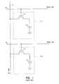
- FIG. 1illustrates a portion of a DRAM memory circuit containing two neighboring DRAM cells 100 .
- Each cell 100contains a storage capacitor 140 and an access field effect transistor or transfer device 120 .
- one side of the storage capacitor 140is connected to a reference voltage (illustrated as a ground potential for convenience purposes).
- the other side of the storage capacitor 140is connected to the drain of the transfer device 120 .
- the gate of the transfer device 120is connected to a signal known in the art as a word line 180 .
- the source of the transfer device 120is connected to a signal known in the art as a bit line 160 (also known in the art as a digit line).
- each cell 100contains one bit of data (i.e., a logic “0” or logic “1”).
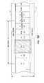
- the DRAM 240contains a memory array 242 , row and column decoders 244 , 248 and a sense amplifier circuit 246 .
- the memory array 242consists of a plurality of memory cells 200 (constructed as illustrated in FIG. 1) whose word lines 280 and bit lines 260 are commonly arranged into rows and columns, respectively.
- the bit lines 260 of the memory array 242are connected to the sense amplifier circuit 246 , while its word lines 280 are connected to the row decoder 244 .
- Address and control signalsare input on address/control lines 261 into the DRAM 240 and connected to the column decoder 248 , sense amplifier circuit 246 and row decoder 244 and are used to gain read and write access, among other things, to the memory array 242 .
- the column decoder 248is connected to the sense amplifier circuit 246 via control and column select signals on column select lines 262 .
- the sense amplifier circuit 246receives input data destined for the memory array 242 and outputs data read from the memory array 242 over input/output (I/O) data lines 263 .
- Datais read from the cells of the memory array 242 by activating a word line 280 (via the row decoder 244 ), which couples all of the memory cells corresponding to that word line to respective bit lines 260 , which define the columns of the array.
- One or more bit lines 260are also activated.
- the sense amplifier circuit 246 connected to a bit line columndetects and amplifies the data bit transferred from the storage capacitor of the memory cell to its bit line 260 by measuring the potential difference between the activated bit line 260 and a reference line which may be an inactive bit line.
- a reference linewhich may be an inactive bit line.
- DRAMsdynamic random access memories
- FETfield-effect transistor
- capacitorwhich functions as a storage element.
- VLSIvery large scale integrated
- One approach to embedded memory technologyis based on the one transistor DRAM cell structure that utilizes the trench process employed in IBM's and Toshiba's DRAMs. (See generally, W. P. Noble et al., “The evolution of IBM CMOS DRAM Technology,” IBM J. Research and Development, 39-1/2, 167-188 (1995)). With trench technology, logic performance is not compromised. Trench technology provides a planar surface topology that enhances interconnect reliability while providing a DRAM storage capacitor with a large and conventional storage capacitance. However, additional masking levels are required in the logic technology to fabricate the trench capacitors.
- FIG. 3Another approach to embedded memory is based on a three transistor DRAM cell structure, shown in FIG. 3.
- the three transistor DRAM cell structurewas developed prior to the use of the trench capacitors or stacked capacitors now used in DRAMs. (See generally, J. Rabaey, Digital Integrated Circuits, Prentice Hall, 585-587 (1996)).
- a much smaller storage capacitorwas utilized and compensated for by the gain of one of the transistors, in other words the first DRAMs developed used gain cells.
- These type of DRAM cellsrequire only a minor modification of the conventional logic technology processes but occupy a large area due to the use of three transistors.
- the inventorshave previously disclosed a DRAM gain cell using two transistors. (See generally, L. Forbes, “Merged Transistor Structure for Gain Memory Cell,” U.S. Pat. No. 5,732,014, issued 24 Mar. 1998, continuation granted as U.S. Pat. No. 5,897,351, issued 27 Apr. 1999). A number of other gain cells have also been disclosed. (See generally, Sunouchi et al., “A self-Amplifying (SEA) Cell for Future High Density DRAMs,” Ext. Abstracts of IEEE Int. Electron Device Meeting, pp. 465-468 (1991); M.
- SEAself-Amplifying
- FIG. 4illustrates a portion of a DRAM memory circuit containing two neighboring gain cells, 401 and 403 . Each gain cell, 401 and 403 , is separated from a substrate 405 by a buried oxide layer 407 .
- the gain cells, 401 and 403are formed on the buried oxide 407 and thus have a floating body, 409 - 1 and 409 - 2 respectively, separating a source region 411 (shared for the two cells) and a drain region 413 - 1 and 413 - 2 .
- a bit/data line 415is coupled to the drain regions 413 - 1 and 413 - 2 via bit contacts, 417 - 1 and 417 - 2 .
- a ground source 419is coupled to the source region 411 .
- Wordlines or gates, 421 - 1 and 421 - 2oppose the floating body regions 409 - 1 and 409 - 2 and are separated therefrom by a gate oxide, 423 - 1 and 423 - 2 .
- back gate biasis used to modulate the threshold voltage and consequently the conductivity of the NMOS transistor in each gain cell.
- the potential of the back gate body, 409 - 1 and 409 - 2is made more positive by avalanche breakdown in the drain regions, 413 - 1 and 413 - 2 , and collection of the holes generated by the body, 409 - 1 and 409 - 2 .
- a more positive potential or forward bias applied to the body, 409 - 1 and 409 - 2decreases the threshold voltage and makes the transistor more conductive when addressed. Charge storage is accomplished by this additional charge stored on the floating body, 409 - 1 and 409 - 2 .
- Resetis accomplished by forward biasing the drain-body n-p junction diode to remove charge from the body.
- a high density horizontally merged MOS-bipolar gain memory cellis realized for DRAM operation.
- the gain cellincludes a horizontal MOS transistor having a source region, a drain region, and a floating body region therebetween.
- the gain cellincludes a horizontal bi-polar transistor having an emitter region, a base region and a collector region.
- the collector region for the horizontal bi-polar transistorserves as the floating body region for the horizontal MOS transistor.
- a gateopposes the floating body region and is separated therefrom by a gate dielectric.
- the emitter region for the horizontal bi-polar transistoris coupled to a write data line.
- the gateis coupled to a read data word line.
- the source regionis coupled to a read data bit line.
- FIG. 1is a circuit diagram illustrating conventional dynamic random access memory (DRAM) cells.
- DRAMdynamic random access memory
- FIG. 2is a block diagram illustrating a DRAM device.
- FIG. 3is a schematic for an embedded memory based on a three transistor DRAM cell structure.
- FIG. 4illustrates two neighboring one transistor gain cells as a portion of a memory array.
- FIG. 5Ais a cross-sectional, perspective view illustrating an embodiment of a horizontally merged MOS-bipolar transistor gain memory cell according to the teachings of the present invention.
- FIG. 5Billustrates a top view of FIG. 5A in planar, CMOS technology with shallow trench oxide isolation.
- FIG. 5Cillustrates an electrical equivalent circuit embodiment of the horizontally merged MOS-bipolar transistor gain memory cell indicating that the floating body well of the horizontal MOS transistor and the well to substrate capacitance acts as a storage capacitor.
- FIG. 6is a block diagram illustrating an embodiment of an electronic system utilizing the embedded gain memory cells of the present invention.
- wafer and substrateare interchangeably used to refer generally to any structure on which integrated circuits are formed, and also to such structures during various stages of integrated circuit fabrication. Both terms include doped and undoped semiconductors, epitaxial layers of a semiconductor on a supporting semiconductor or insulating material, combinations of such layers, as well as other such structures that are known in the art.
- the term “horizontal” as used in this applicationis defined as a plane parallel to the conventional plane or surface of a wafer or substrate, regardless of the orientation of the wafer or substrate.
- the term “vertical”refers to a direction perpendicular to the horizontal as defined above. Prepositions, such as “on”, “side” (as in “sidewall”), “higher”, “lower”, “over” and “under” are defined with respect to the conventional plane or surface being on the top surface of the wafer or substrate, regardless of the orientation of the wafer or substrate.
- FIG. 5Ais a cross-sectional, perspective view illustrating an embodiment of an embedded, horizontally merged MOS-bipolar transistor gain memory cell 501 according to the teachings of the present invention.
- the embedded, horizontally merged MOS-bipolar transistor gain memory cell 501is formed in a p-type conductivity substrate 502 .
- An n-type conductivity well 505is formed in the p-type conductivity substrate 502 .
- a more heavily doped p-type conductivity region (p+) 507is formed in a portion of the p-type conductivity substrate 502 and in a portion of the n-type conductivity well 505 .
- the more heavily doped p-type conductivity region (p+) 507serves as a source region 507 for a horizontal MOS transistor 509 portion of the horizontally merged MOS-bipolar transistor gain memory cell 501 .
- Another more heavily doped p-type conductivity region (p+) 511is formed in another portion of the n-type conductivity well 505 .
- This more heavily doped p-type conductivity region (p+) 511serves as the drain region 511 for the horizontal MOS transistor 509 portion of the horizontally merged MOS-bipolar transistor gain memory cell 501 .
- a gate 513opposes the n-type conductivity well 505 between the source and the drain regions, 507 and 511 respectively.
- the n-type conductivity well 505serves as a body region 505 and, more particularly, as a floating body region 505 for the horizontal MOS transistor 509 portion of the horizontally merged MOS-bipolar transistor gain memory cell 501 .
- the n-type conductivity well 505can also be referred to as a floating body n-well 505 .
- the gate 513is separated from the floating body region 505 by a gate dielectric 515 .
- a read data word line 517is coupled to the gate 513 along rows of an array.
- any number of the horizontally merged MOS-bipolar transistor gain memory cell 501 shown in FIG. 5Acan be arranged in an array on a semiconductor wafer.
- a read data bit line 519is coupled to the drain region 511 along columns of such an array.
- a horizontal bi-polar transistor 521completes the horizontally merged MOS-bipolar transistor gain memory cell 501 .
- the horizontal bi-polar transistor 521includes an emitter region 523 , a base region 525 , and a collector region 527 .
- the emitter region 523includes a heavily doped n-type conductivity region 523 (n+) formed in the p-type conductivity substrate 502 .
- the emitter regioncan also be referred to as an injector 523 .
- the base region 525 for the horizontal bi-polar transistor 521 portion of theis formed by the p-type conductivity substrate material.
- the base region 525 and the p-type conductivity substrate 502are coupled to a ground potential.
- the collector region 527 for the horizontal bi-polar transistor 521is formed from a portion of the floating body n-well 505 .
- the p+ drain region 511is formed in the floating body n-well 505 and a portion of the floating body n-well 505 extends and/or wraps around the p+ drain region 511 to a side of the drain region 511 horizontally opposite from the side of the drain region 511 where the gate 513 is located.
- the floating body n-well 505serves both as a floating body region 505 for the horizontal MOS transistor 509 and a portion of the floating body n-well also serves as the collector region 527 of the horizontal bi-polar transistor 521 .
- a write data bit line 529is coupled to the emitter region 523 for the horizontal bi-polar transistor 521 portion of the horizontally merged MOS-bipolar transistor gain memory cell 501 .
- the write data bit line 529can also be referred to as an emitter line 529 and/or an injector line 529 .
- the horizontal bi-polar transistor 521is operable to inject a charge on to the floating body 505 of the horizontal MOS transistor 509 .
- the floating body 505is operable to store charge by capacitive coupling to the gate 513 and a small stored charge from the same produces a change in the threshold voltage of the horizontal MOS transistor 509 .
- the horizontally merged MOS-bipolar transistor gain memory cell 501can be formed or fabricated using planar CMOS processing techniques. As such, the present invention yields a horizontally merged MOS-bipolar transistor gain memory cell 501 which has an area equal to or less than 10 square photolithographic features (10F 2 ).
- FIG. 5Billustrates a top view of FIG. 5A in planar, CMOS technology with shallow trench oxide isolation 531 illustrated alongside the horizontally merged MOS-bipolar transistor gain memory cell 501 .
- the top view of FIG. 5Aillustrates the heavily doped p-type conductivity source region 507 (p+).
- the gate 513is shown above the floating body region 505 of the horizontal MOS transistor 509 portion of the horizontally merged MOS-bipolar transistor gain memory cell 501 .
- the portion of the floating body n-well 505 which serves as the collector region 527 for the horizontal bi-polar transistor 521is seen from the top view on the opposite side of the drain region 511 from the gate's 513 location. From the top view embodiment of FIG. 5A, the p-type conductivity portion of the substrate which serves as the base region 525 for the horizontal bi-polar transistor 521 is viewable adjacent to the collector region 527 .
- the heavily doped n-type conductivity emitter region, or injector, 523 (n+)is viewable adjacent to the base region 525 .
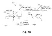
- FIG. 5Cillustrates an electrical equivalent circuit embodiment of the horizontally merged MOS-bipolar transistor gain memory cell 501 indicating that the floating body well 505 of the horizontal MOS transistor 509 and the floating body well 505 to substrate 502 capacitance acts as a storage capacitor 533 .
- the embodiment of FIG. 5Cillustrates the horizontal MOS transistor 509 including the source region 507 , the gate 513 opposing the floating body region 505 , and the drain region 511 .
- a read data word line 517is shown coupled to the gate 513 and a read data bit line 519 is coupled to the drain region 511 .
- FIG. 5Cfurther illustrates the bi-polar transistor 521 including the collector region 527 , which is integrally formed with the floating body region 505 , the base region 525 , and the emitter, or injector, region 523 .
- the emitter region 523is coupled to a write data bit line, emitter line, or injector line 529 .
- the base region 525 of the bi-polar transistor 521which is integrally formed with the substrate 502 , is coupled to a ground potential.
- the floating body well 505 of the horizontal MOS transistor and the floating body well 505 to substrate 502 capacitanceacts as a storage capacitor 533 .
- the sense device used to read the horizontally merged MOS-bipolar transistor gain memory cell 501is the horizontal MOS transistor 509 which is addressed by the read data word line 517 .
- the horizontal MOS transistor 509In the embodiment of a horizontal PMOS transistor 509 , if a negative charge or electrons are stored on the floating body 505 , then the n-type floating body 505 will be slightly forward biased and the horizontal MOS transistor 509 will be more conductive than normal.
- the horizontal bi-polar transistor 521is an npn bi-polar transistor 521 .
- the horizontal bi-polar transistor 521need not be a high performance device nor have a high current gain. Accordingly, the horizontal bi-polar transistor 521 can be a high yield structure.
- the read data word line 517is driven positive to drive the floating n-type body 505 to a positive potential by capacitive coupling to the read data word line 517 .
- This positive potentialserves to keep the floating body 505 reverse biased and avoid charge leakage.
- the horizontally merged MOS-bipolar transistor gain memory cell 501can be erased by driving the drain 511 positive and the gate 513 negative to forward bias the drain-body p-n junction ( 511 - 505 junction).
- the drain-body p-n junction511 - 505 junction.
- T. Ohsawa et al.“Memory Design Using One Transistor Gain Cell on SOI,” IEEE Int. Solid State Circuits Conv ., San Francisco, 152-153 (2002); S. Okhonin, M. Nagoga, J. M. Sallese, P. Fazan, “A SOI Capacitor-less IT-DRAM Cell,” Late News 2001 IEEE Intl. SOI Conference , Durango, Colo., 153-154).
- the horizontally merged MOS-bipolar transistor gain memory cell 501can provide a very high gain and amplification of the stored charge on the floating body 505 of the horizontal, or lateral, PMOS sense transistor 509 .
- a small change in the threshold voltage caused by charge stored on the floating body 505will result in a large difference in the number of holes conducted between the drain 511 and source of 507 the horizontal PMOS sense transistor 509 during the read data operation.
- This amplificationallows the small storage capacitance of the sense amplifier floating body 505 to be used instead of a large stacked capacitor storage capacitance.
- the resulting horizontally merged MOS-bipolar transistor gain memory cell 501has a very high density with a cell area of approximately 10F 2 , where F is the minimum feature size, and whose vertical extent is far less than the total height of a stacked capacitor or trench capacitor cell and access transistor.
- the cellcan be fabricated without any modification of conventional CMOS logic technology.
- the sense transistor 509would be an NMOS transistor with a p-type floating body.
- FIG. 6is a block diagram of a processor-based system 600 utilizing embedded, horizontally merged MOS-bipolar transistor gain memory cells according to the various embodiments of the present invention. That is, the system 600 utilizes various embodiments of the horizontally merged MOS-bipolar transistor gain memory cell 501 illustrated in FIGS. 5 A- 5 C.
- the processor-based system 600may be a computer system, a process control system or any other system employing a processor and associated memory.
- the system 600includes a central processing unit (CPU) 602 , e.g., a microprocessor, that communicates with the RAM 612 and an I/O device 608 over a bus 620 .
- CPUcentral processing unit
- bus 620may be a series of buses and bridges commonly used in a processor-based system, but for convenience purposes only, the bus 620 has been illustrated as a single bus.
- a second I/O device 610is illustrated, but is not necessary to practice the invention.
- the processor-based system 600can further include read-only memory (ROM) 614 and can include peripheral devices such as a floppy disk drive 604 and a compact disk (CD) ROM drive 606 that also communicates with the CPU 602 over the bus 620 as is well known in the art.
- ROMread-only memory
- CDcompact disk
- FIG. 6illustrates an embodiment for electronic system circuitry in which the novel embedded, horizontally merged MOS-bipolar transistor gain memory cell 501 of the present invention are used.
- the illustration of system 600is intended to provide a general understanding of one application for the structure and circuitry of the present invention, and is not intended to serve as a complete description of all the elements and features of an electronic system using the novel horizontally merged MOS-bipolar transistor gain memory cell 501 structures.
- the inventionis equally applicable to any size and type of system 600 using the novel horizontally merged MOS-bipolar transistor gain memory cells of the present invention and is not intended to be limited to that described above.
- such an electronic systemcan be fabricated in single-package processing units, or even on a single semiconductor chip, in order to reduce the communication time between the processor and the memory device.
- Applications containing the embedded, horizontally merged MOS-bipolar transistor gain memory cells of the present invention as described in this disclosureinclude electronic systems for use in memory modules, device drivers, power modules, communication modems, processor modules, and application-specific modules, and may include multilayer, multichip modules.
- Such circuitrycan further be a subcomponent of a variety of electronic systems, such as a clock, a television, a cell phone, a personal computer, an automobile, an industrial control system, an aircraft, and others.
- the embedded, horizontally merged MOS-bipolar transistor gain memory cell of the present inventioncan provide a very high gain and amplification of a stored charge on the floating body of the horizontal MOS sense transistor.
- a small change in the threshold voltage caused by charge stored on the floating bodywill result in a large difference in the number of holes conducted between the drain and source of the horizontal MOS sense transistor during the read data operation.
- This amplificationallows the small storage capacitance of the sense amplifier floating body to be used instead of a large stacked capacitor storage capacitance.
- the resulting cellhas a very high density with a cell area of 10F 2 , where F is the minimum feature size, and whose horizontal extent is far less than the total height of a stacked capacitor or trench capacitor cell and access transistor.
Landscapes
- Semiconductor Memories (AREA)
- Dram (AREA)
Abstract
Description
- This application is related to the following commonly assigned U.S. patent applications: “Single Transistor Vertical Memory Gain Cell,” Ser. No. 10/231,397, filed Aug. 29, 2002, “Merged MOS-Bipolar Capacitor Memory Cell,” Ser. No. 10/230,929, filed Aug. 29, 2002, each of which disclosure is herein incorporated by reference.[0001]
- The present invention relates generally to integrated circuits, and in particular to an embedded DRAM gain memory cell.[0002]
- An essential semiconductor device is semiconductor memory, such as a random access memory (RAM) device. A RAM device allows the user to execute both read and write operations on its memory cells. Typical examples of RAM devices include dynamic random access memory (DRAM) and static random access memory (SRAM).[0003]
- DRAM is a specific category of RAM containing an array of individual memory cells, where each cell includes a capacitor for holding a charge and a transistor for accessing the charge held in the capacitor. The transistor is often referred to as the access transistor or the transfer device of the DRAM cell.[0004]
- FIG. 1 illustrates a portion of a DRAM memory circuit containing two neighboring[0005]
DRAM cells 100. Eachcell 100 contains astorage capacitor 140 and an access field effect transistor ortransfer device 120. For each cell, one side of thestorage capacitor 140 is connected to a reference voltage (illustrated as a ground potential for convenience purposes). The other side of thestorage capacitor 140 is connected to the drain of thetransfer device 120. The gate of thetransfer device 120 is connected to a signal known in the art as aword line 180. The source of thetransfer device 120 is connected to a signal known in the art as a bit line160 (also known in the art as a digit line). With thememory cell 100 components connected in this manner, it is apparent that theword line 180 controls access to thestorage capacitor 140 by allowing or preventing the signal (representing a logic “0” or a logic “1”) carried on thebit line 160 to be written to or read from thestorage capacitor 140. Thus, eachcell 100 contains one bit of data (i.e., a logic “0” or logic “1”). - In FIG. 2 a[0006]
DRAM circuit 240 is illustrated. TheDRAM 240 contains amemory array 242, row andcolumn decoders sense amplifier circuit 246. Thememory array 242 consists of a plurality of memory cells200 (constructed as illustrated in FIG. 1) whoseword lines 280 andbit lines 260 are commonly arranged into rows and columns, respectively. Thebit lines 260 of thememory array 242 are connected to thesense amplifier circuit 246, while itsword lines 280 are connected to therow decoder 244. Address and control signals are input on address/control lines 261 into theDRAM 240 and connected to thecolumn decoder 248,sense amplifier circuit 246 androw decoder 244 and are used to gain read and write access, among other things, to thememory array 242. - The[0007]
column decoder 248 is connected to thesense amplifier circuit 246 via control and column select signals on columnselect lines 262. Thesense amplifier circuit 246 receives input data destined for thememory array 242 and outputs data read from thememory array 242 over input/output (I/O)data lines 263. Data is read from the cells of thememory array 242 by activating a word line280 (via the row decoder244), which couples all of the memory cells corresponding to that word line torespective bit lines 260, which define the columns of the array. One ormore bit lines 260 are also activated. When aparticular word line 280 andbit lines 260 are activated, thesense amplifier circuit 246 connected to a bit line column detects and amplifies the data bit transferred from the storage capacitor of the memory cell to itsbit line 260 by measuring the potential difference between theactivated bit line 260 and a reference line which may be an inactive bit line. The operation of DRAM sense amplifiers is described, for example, in U.S. Pat. Nos. 5,627,785; 5,280,205; and 5,042,011, all assigned to Micron Technology Inc., and incorporated by reference herein. - The memory cells of dynamic random access memories (DRAMs) are comprised of two main components, a field-effect transistor (FET) and a capacitor which functions as a storage element. The need to increase the storage capability of semiconductor memory devices has led to the development of very large scale integrated (VLSI) cells which provides a substantial increase in component density. As component density has increased, cell capacitance has had to be decreased because of the need to maintain isolation between adjacent devices in the memory array. However, reduction in memory cell capacitance reduces the electrical signal output from the memory cells, making detection of the memory cell output signal more difficult. Thus, as the density of DRAM devices increases, it becomes more and more difficult to obtain reasonable storage capacity.[0008]
- As DRAM devices are projected as operating in the gigabit range, the ability to form such a large number of storage capacitors requires smaller areas. However, this conflicts with the requirement for larger capacitance because capacitance is proportional to area. Moreover, the trend for reduction in power supply voltages results in stored charge reduction and leads to degradation of immunity to alpha particle induced soft errors, both of which require that the storage capacitance be even larger.[0009]
- By using embedded memory rather than external memory, designers can maximize memory throughput to achieve higher system performance, introduce innovative architectures with customized memory sizes, and reduce power consumption in their systems. (See generallly, H. Takato et al., “Process Integration Trends for Embedded DRAM,”[0010]Proceedings of UlSI Process Integration, Electrochemical Society Proceedings,99-18, 107-19 (1999); M. Mukai et al., “Proposal of a Logic Compatible Merged-Type Gain Cell for High Density Embedded.,”IEEE Trans. on Electron Devices,46-6, 1201-1206 (1999)). Designers will also benefit from less expensive packaging, by removing the extra pins that drive external memory and by eliminating board space otherwise required by external memory chips. Both of these benefits can lower production costs. In addition, using embedded memory ensures users of a guaranteed supply of this type of memory, without the volatility of the external memory market.
- One approach to embedded memory technology is based on the one transistor DRAM cell structure that utilizes the trench process employed in IBM's and Toshiba's DRAMs. (See generally, W. P. Noble et al., “The evolution of IBM CMOS DRAM Technology,”[0011]IBM J. Research and Development,39-1/2, 167-188 (1995)). With trench technology, logic performance is not compromised. Trench technology provides a planar surface topology that enhances interconnect reliability while providing a DRAM storage capacitor with a large and conventional storage capacitance. However, additional masking levels are required in the logic technology to fabricate the trench capacitors.
- Another approach to embedded memory is based on a three transistor DRAM cell structure, shown in FIG. 3. The three transistor DRAM cell structure was developed prior to the use of the trench capacitors or stacked capacitors now used in DRAMs. (See generally, J. Rabaey, Digital Integrated Circuits, Prentice Hall, 585-587 (1996)). A much smaller storage capacitor was utilized and compensated for by the gain of one of the transistors, in other words the first DRAMs developed used gain cells. These type of DRAM cells require only a minor modification of the conventional logic technology processes but occupy a large area due to the use of three transistors.[0012]
- The inventors have previously disclosed a DRAM gain cell using two transistors. (See generally, L. Forbes, “Merged Transistor Structure for Gain Memory Cell,” U.S. Pat. No. 5,732,014, issued 24 Mar. 1998, continuation granted as U.S. Pat. No. 5,897,351, issued 27 Apr. 1999). A number of other gain cells have also been disclosed. (See generally, Sunouchi et al., “A self-Amplifying (SEA) Cell for Future High Density DRAMs,” Ext. Abstracts of IEEE Int. Electron Device Meeting, pp. 465-468 (1991); M. Terauchi et al., “A Surrounding Gate Transistor (SGT) Gain Cell for Ultra High Density DRAMS,” VLSI Tech. Symposium, pp. 21-22 (1993); S. Shukuri et al., “Super-Low-Voltage Operation of a Semi-Static Complementary Gain RAM Memory Cell,” VLSI Tech. Symposium pp. 23-24 (1993); S. Shukuri et al., “Super-low-voltage operation of a semi-static complementary gain DRAM memory cell,” Ext. Abs. of IEEE Int. Electron Device Meeting, pp. 1006-1009 (1992); S. Shukuri et al., “A Semi-Static Complementary Gain Cell Technology for Sub-1 V Supply DRAM's,” IEEE Trans. on Electron Devices, Vol. 41, pp. 926-931 (1994); H. Wann and C. Hu, “A Capacitorless DRAM Cell on SOI Substrate,” Ext. Abs. IEEE Int. Electron Devices Meeting, pp. 635-638; W. Kim et al., “An Experimental High-Density DRAM Cell with a Built-in Gain Stage,” IEEE J. of Solid-State Circuits, Vol. 29, pp. 978-981 (1994); W. H. Krautschneider et al., “Planar Gain Cell for Low Voltage Operation and Gigabit Memories,” Proc. VLSI Technology Symposium, pp. 139-140 (1995); D. M. Kenney, “Charge Amplifying trench Memory Cell,” U.S. Pat. No. 4,970,689, 13 Nov. 1990; M. Itoh, “Semiconductor memory element and method of fabricating the same,” U.S. Pat. No. 5,220,530, 15 Jun. 1993; W. H. Krautschneider et al., “Process for the Manufacture of a high density Cell Array of Gain Memory Cells,” U.S. Pat. No. 5,308,783, 3 May 1994; C. Hu et al., “Capacitorless DRAM device on Silicon on Insulator Substrate,” U.S. Pat. No. 5,448,513, 5 Sept. 1995; S. K. Banerjee, “Method of making a Trench DRAM cell with Dynamic Gain,” U.S. Pat. No. 5,066,607, 19 Nov. 1991; S. K. Banerjee, “Trench DRAM cell with Dynamic Gain,” U.S. Pat. No. 4,999,811, 12 Mar. 1991; Lim et al., “Two transistor DRAM cell,” U.S. Pat. No. 5,122,986, 16 Jun. 1992).[0013]
- Recently a one transistor gain cell has been reported as shown in FIG. 4. (See generally, T. Ohsawa et al., “Memory design using one transistor gain cell on SOI,” IEEE Int. Solid State Circuits Conference, San Francisco, 2002, pp. 152-153). FIG. 4 illustrates a portion of a DRAM memory circuit containing two neighboring gain cells,[0014]401 and403. Each gain cell,401 and403, is separated from a
substrate 405 by a buriedoxide layer 407. The gain cells,401 and403, are formed on the buriedoxide 407 and thus have a floating body,409-1 and409-2 respectively, separating a source region411 (shared for the two cells) and a drain region413-1 and413-2. A bit/data line 415 is coupled to the drain regions413-1 and413-2 via bit contacts,417-1 and417-2. Aground source 419 is coupled to thesource region 411. Wordlines or gates,421 -1 and421-2, oppose the floating body regions409-1 and409-2 and are separated therefrom by a gate oxide,423-1 and423-2. - In the gain cell shown in FIG. 4 a floating body,[0015]409-1 and409-2, back gate bias is used to modulate the threshold voltage and consequently the conductivity of the NMOS transistor in each gain cell. The potential of the back gate body,409-1 and409-2, is made more positive by avalanche breakdown in the drain regions,413-1 and413-2, and collection of the holes generated by the body,409-1 and409-2. A more positive potential or forward bias applied to the body,409-1 and409-2, decreases the threshold voltage and makes the transistor more conductive when addressed. Charge storage is accomplished by this additional charge stored on the floating body,409-1 and409-2. Reset is accomplished by forward biasing the drain-body n-p junction diode to remove charge from the body.
- Still, there is a need in the art for improved DRAM cell structures which can be based entirely on conventional CMOS logic technology, without additional masking and process steps, and which have a minimal cell area.[0016]
- The above mentioned problems with conventional memories and other problems are addressed by the present invention and will be understood by reading and studying the following specification. An embedded, high density horizontally merged MOS-bipolar gain memory cell is realized for DRAM operation.[0017]
- In one embodiment of the present invention, a high density horizontally merged MOS-bipolar gain memory cell is realized for DRAM operation. The gain cell includes a horizontal MOS transistor having a source region, a drain region, and a floating body region therebetween. The gain cell includes a horizontal bi-polar transistor having an emitter region, a base region and a collector region. The collector region for the horizontal bi-polar transistor serves as the floating body region for the horizontal MOS transistor. A gate opposes the floating body region and is separated therefrom by a gate dielectric. The emitter region for the horizontal bi-polar transistor is coupled to a write data line. The gate is coupled to a read data word line. The source region is coupled to a read data bit line.[0018]
- These and other embodiments, aspects, advantages, and features of the present invention will be set forth in part in the description which follows, and in part will become apparent to those skilled in the art by reference to the following description of the invention and referenced drawings or by practice of the invention. The aspects, advantages, and features of the invention are realized and attained by means of the instrumentalities, procedures, and combinations particularly pointed out in the appended claims.[0019]
- FIG. 1 is a circuit diagram illustrating conventional dynamic random access memory (DRAM) cells.[0020]
- FIG. 2 is a block diagram illustrating a DRAM device.[0021]
- FIG. 3 is a schematic for an embedded memory based on a three transistor DRAM cell structure.[0022]
- FIG. 4 illustrates two neighboring one transistor gain cells as a portion of a memory array.[0023]
- FIG. 5A is a cross-sectional, perspective view illustrating an embodiment of a horizontally merged MOS-bipolar transistor gain memory cell according to the teachings of the present invention.[0024]
- FIG. 5B illustrates a top view of FIG. 5A in planar, CMOS technology with shallow trench oxide isolation.[0025]
- FIG. 5C illustrates an electrical equivalent circuit embodiment of the horizontally merged MOS-bipolar transistor gain memory cell indicating that the floating body well of the horizontal MOS transistor and the well to substrate capacitance acts as a storage capacitor.[0026]
- FIG. 6 is a block diagram illustrating an embodiment of an electronic system utilizing the embedded gain memory cells of the present invention.[0027]
- In the following detailed description of the invention, reference is made to the accompanying drawings which form a part hereof, and in which is shown, by way of illustration, specific embodiments in which the invention may be practiced. The embodiments are intended to describe aspects of the invention in sufficient detail to enable those skilled in the art to practice the invention. Other embodiments may be utilized and changes may be made without departing from the scope of the present invention. In the following description, the terms wafer and substrate are interchangeably used to refer generally to any structure on which integrated circuits are formed, and also to such structures during various stages of integrated circuit fabrication. Both terms include doped and undoped semiconductors, epitaxial layers of a semiconductor on a supporting semiconductor or insulating material, combinations of such layers, as well as other such structures that are known in the art.[0028]
- The term “horizontal” as used in this application is defined as a plane parallel to the conventional plane or surface of a wafer or substrate, regardless of the orientation of the wafer or substrate. The term “vertical” refers to a direction perpendicular to the horizontal as defined above. Prepositions, such as “on”, “side” (as in “sidewall”), “higher”, “lower”, “over” and “under” are defined with respect to the conventional plane or surface being on the top surface of the wafer or substrate, regardless of the orientation of the wafer or substrate. The following detailed description is, therefore, not to be taken in a limiting sense, and the scope of the present invention is defined only by the appended claims, along with the full scope of equivalents to which such claims are entitled.[0029]
- FIG. 5A is a cross-sectional, perspective view illustrating an embodiment of an embedded, horizontally merged MOS-bipolar transistor[0030]
gain memory cell 501 according to the teachings of the present invention. In the embodiment of FIG. 5A, the embedded, horizontally merged MOS-bipolar transistorgain memory cell 501 is formed in a p-type conductivity substrate 502. An n-type conductivity well 505 is formed in the p-type conductivity substrate 502. A more heavily doped p-type conductivity region (p+)507 is formed in a portion of the p-type conductivity substrate 502 and in a portion of the n-type conductivity well 505. The more heavily doped p-type conductivity region (p+)507 serves as asource region 507 for ahorizontal MOS transistor 509 portion of the horizontally merged MOS-bipolar transistorgain memory cell 501. - Another more heavily doped p-type conductivity region (p+)[0031]511 is formed in another portion of the n-
type conductivity well 505. This more heavily doped p-type conductivity region (p+)511 serves as thedrain region 511 for thehorizontal MOS transistor 509 portion of the horizontally merged MOS-bipolar transistorgain memory cell 501. Agate 513 opposes the n-type conductivity well505 between the source and the drain regions,507 and511 respectively. As one of ordinary skill in the art will understand upon reading this disclosure, the n-type conductivity well 505 serves as abody region 505 and, more particularly, as a floatingbody region 505 for thehorizontal MOS transistor 509 portion of the horizontally merged MOS-bipolar transistorgain memory cell 501. The n-type conductivity well505 can also be referred to as a floating body n-well505. - The[0032]
gate 513 is separated from the floatingbody region 505 by agate dielectric 515. As shown in the embodiment of FIG. 5A, a readdata word line 517 is coupled to thegate 513 along rows of an array. As one of ordinary skill in the art will appreciate upon reading this disclosure, any number of the horizontally merged MOS-bipolar transistorgain memory cell 501 shown in FIG. 5A can be arranged in an array on a semiconductor wafer. A readdata bit line 519 is coupled to thedrain region 511 along columns of such an array. - As shown in FIG. 5A, a horizontal[0033]
bi-polar transistor 521 completes the horizontally merged MOS-bipolar transistorgain memory cell 501. The horizontalbi-polar transistor 521 includes anemitter region 523, abase region 525, and acollector region 527. As shown in the embodiment of FIG. 5A, theemitter region 523 includes a heavily doped n-type conductivity region523 (n+) formed in the p-type conductivity substrate 502. The emitter region can also be referred to as aninjector 523. In FIG. 5A, thebase region 525 for the horizontalbi-polar transistor 521 portion of the is formed by the p-type conductivity substrate material. In some embodiments, thebase region 525 and the p-type conductivity substrate 502 are coupled to a ground potential. - According to the teachings of the present invention, the[0034]
collector region 527 for the horizontalbi-polar transistor 521 is formed from a portion of the floating body n-well505. In the embodiment shown in FIG. 5A, thep+ drain region 511 is formed in the floating body n-well505 and a portion of the floating body n-well505 extends and/or wraps around thep+ drain region 511 to a side of thedrain region 511 horizontally opposite from the side of thedrain region 511 where thegate 513 is located. In this manner, the floating body n-well505 serves both as a floatingbody region 505 for thehorizontal MOS transistor 509 and a portion of the floating body n-well also serves as thecollector region 527 of the horizontalbi-polar transistor 521. - As shown in the embodiment of FIG. 5A, a write[0035]
data bit line 529 is coupled to theemitter region 523 for the horizontalbi-polar transistor 521 portion of the horizontally merged MOS-bipolar transistorgain memory cell 501. The writedata bit line 529 can also be referred to as anemitter line 529 and/or aninjector line 529. According to the teachings of the present invention, the horizontalbi-polar transistor 521 is operable to inject a charge on to the floatingbody 505 of thehorizontal MOS transistor 509. The floatingbody 505 is operable to store charge by capacitive coupling to thegate 513 and a small stored charge from the same produces a change in the threshold voltage of thehorizontal MOS transistor 509. As one of ordinary skill in the art will appreciate upon reading this disclosure, the horizontally merged MOS-bipolar transistorgain memory cell 501 can be formed or fabricated using planar CMOS processing techniques. As such, the present invention yields a horizontally merged MOS-bipolar transistorgain memory cell 501 which has an area equal to or less than 10 square photolithographic features (10F2). - FIG. 5B illustrates a top view of FIG. 5A in planar, CMOS technology with shallow[0036]
trench oxide isolation 531 illustrated alongside the horizontally merged MOS-bipolar transistorgain memory cell 501. The top view of FIG. 5A illustrates the heavily doped p-type conductivity source region507 (p+). Thegate 513 is shown above the floatingbody region 505 of thehorizontal MOS transistor 509 portion of the horizontally merged MOS-bipolar transistorgain memory cell 501. On the other side of thegate 513 is shown the heavily doped p-type conductivity drain region511 (p+). The portion of the floating body n-well505 which serves as thecollector region 527 for the horizontalbi-polar transistor 521 is seen from the top view on the opposite side of thedrain region 511 from the gate's513 location. From the top view embodiment of FIG. 5A, the p-type conductivity portion of the substrate which serves as thebase region 525 for the horizontalbi-polar transistor 521 is viewable adjacent to thecollector region 527. The heavily doped n-type conductivity emitter region, or injector,523 (n+) is viewable adjacent to thebase region 525. On the other side of theemitter region 523, another portion of thesubstrate 502 which serves as thebase region 525 for an adjacent horizontalbi-polar transistor 521 portion of a row adjacent horizontally merged MOS-bipolar transistor gain memory cell is viewable as well as another portion of a neighboring floating body n-well. - FIG. 5C illustrates an electrical equivalent circuit embodiment of the horizontally merged MOS-bipolar transistor[0037]
gain memory cell 501 indicating that the floating body well505 of thehorizontal MOS transistor 509 and the floating body well505 tosubstrate 502 capacitance acts as astorage capacitor 533. The embodiment of FIG. 5C illustrates thehorizontal MOS transistor 509 including thesource region 507, thegate 513 opposing the floatingbody region 505, and thedrain region 511. A readdata word line 517 is shown coupled to thegate 513 and a readdata bit line 519 is coupled to thedrain region 511. - The embodiment of FIG. 5C further illustrates the[0038]
bi-polar transistor 521 including thecollector region 527, which is integrally formed with the floatingbody region 505, thebase region 525, and the emitter, or injector,region 523. As shown in the embodiement of FIG. 5C, theemitter region 523 is coupled to a write data bit line, emitter line, orinjector line 529. As shown in the embodiment of FIG. 5C, in some embodiments thebase region 525 of thebi-polar transistor 521, which is integrally formed with thesubstrate 502, is coupled to a ground potential. And, as indicated above, the floating body well505 of the horizontal MOS transistor and the floating body well505 tosubstrate 502 capacitance acts as astorage capacitor 533. - In operation, the sense device used to read the horizontally merged MOS-bipolar transistor[0039]
gain memory cell 501 is thehorizontal MOS transistor 509 which is addressed by the readdata word line 517. In the embodiment of ahorizontal PMOS transistor 509, if a negative charge or electrons are stored on the floatingbody 505, then the n-type floating body 505 will be slightly forward biased and thehorizontal MOS transistor 509 will be more conductive than normal. - According to the teachings of the present invention, charge is injected on to the floating[0040]
body 505 of thehorizontal MOS transistor 509 by the horizontal, or lateral,bi-polar transistor 521. In the embodiment describe here, the horizontalbi-polar transistor 521 is an npnbi-polar transistor 521. The horizontalbi-polar transistor 521 need not be a high performance device nor have a high current gain. Accordingly, the horizontalbi-polar transistor 521 can be a high yield structure. - During standby the read[0041]
data word line 517 is driven positive to drive the floating n-type body 505 to a positive potential by capacitive coupling to the readdata word line 517. This positive potential serves to keep the floatingbody 505 reverse biased and avoid charge leakage. - The horizontally merged MOS-bipolar transistor[0042]
gain memory cell 501 can be erased by driving thedrain 511 positive and thegate 513 negative to forward bias the drain-body p-n junction (511-505 junction). (See generally, T. Ohsawa et al., “Memory Design Using One Transistor Gain Cell on SOI,”IEEE Int. Solid State Circuits Conv., San Francisco, 152-153 (2002); S. Okhonin, M. Nagoga, J. M. Sallese, P. Fazan, “A SOI Capacitor-less IT-DRAM Cell,”Late News2001IEEE Intl. SOI Conference, Durango, Colo., 153-154). - The horizontally merged MOS-bipolar transistor[0043]
gain memory cell 501 can provide a very high gain and amplification of the stored charge on the floatingbody 505 of the horizontal, or lateral,PMOS sense transistor 509. A small change in the threshold voltage caused by charge stored on the floatingbody 505 will result in a large difference in the number of holes conducted between thedrain 511 and source of507 the horizontalPMOS sense transistor 509 during the read data operation. - This amplification allows the small storage capacitance of the sense[0044]
amplifier floating body 505 to be used instead of a large stacked capacitor storage capacitance. The resulting horizontally merged MOS-bipolar transistorgain memory cell 501 has a very high density with a cell area of approximately 10F2, where F is the minimum feature size, and whose vertical extent is far less than the total height of a stacked capacitor or trench capacitor cell and access transistor. The cell can be fabricated without any modification of conventional CMOS logic technology. - While the description here has been given for a p-type substrate an alternative embodiment would work equally well with n-type or silicon-on-insulator substrates. In that case the[0045]
sense transistor 509 would be an NMOS transistor with a p-type floating body. - System Level[0046]
- FIG. 6 is a block diagram of a processor-based[0047]
system 600 utilizing embedded, horizontally merged MOS-bipolar transistor gain memory cells according to the various embodiments of the present invention. That is, thesystem 600 utilizes various embodiments of the horizontally merged MOS-bipolar transistorgain memory cell 501 illustrated in FIGS.5A-5C. The processor-basedsystem 600 may be a computer system, a process control system or any other system employing a processor and associated memory. Thesystem 600 includes a central processing unit (CPU)602, e.g., a microprocessor, that communicates with the RAM612 and an I/O device 608 over abus 620. It must be noted that thebus 620 may be a series of buses and bridges commonly used in a processor-based system, but for convenience purposes only, thebus 620 has been illustrated as a single bus. A second I/O device610 is illustrated, but is not necessary to practice the invention. The processor-basedsystem 600 can further include read-only memory (ROM)614 and can include peripheral devices such as afloppy disk drive 604 and a compact disk (CD)ROM drive 606 that also communicates with theCPU 602 over thebus 620 as is well known in the art. - It will be appreciated by those skilled in the art that additional circuitry and control signals can be provided, and that the processor-based[0048]
system 600 has been simplified to help focus on the invention. - It will be understood that the embodiment shown in FIG. 6 illustrates an embodiment for electronic system circuitry in which the novel embedded, horizontally merged MOS-bipolar transistor[0049]
gain memory cell 501 of the present invention are used. The illustration ofsystem 600, as shown in FIG. 6, is intended to provide a general understanding of one application for the structure and circuitry of the present invention, and is not intended to serve as a complete description of all the elements and features of an electronic system using the novel horizontally merged MOS-bipolar transistorgain memory cell 501 structures. Further, the invention is equally applicable to any size and type ofsystem 600 using the novel horizontally merged MOS-bipolar transistor gain memory cells of the present invention and is not intended to be limited to that described above. As one of ordinary skill in the art will understand, such an electronic system can be fabricated in single-package processing units, or even on a single semiconductor chip, in order to reduce the communication time between the processor and the memory device. - Applications containing the embedded, horizontally merged MOS-bipolar transistor gain memory cells of the present invention as described in this disclosure include electronic systems for use in memory modules, device drivers, power modules, communication modems, processor modules, and application-specific modules, and may include multilayer, multichip modules. Such circuitry can further be a subcomponent of a variety of electronic systems, such as a clock, a television, a cell phone, a personal computer, an automobile, an industrial control system, an aircraft, and others.[0050]
- The embedded, horizontally merged MOS-bipolar transistor gain memory cell of the present invention can provide a very high gain and amplification of a stored charge on the floating body of the horizontal MOS sense transistor. A small change in the threshold voltage caused by charge stored on the floating body will result in a large difference in the number of holes conducted between the drain and source of the horizontal MOS sense transistor during the read data operation. This amplification allows the small storage capacitance of the sense amplifier floating body to be used instead of a large stacked capacitor storage capacitance. The resulting cell has a very high density with a cell area of 10F[0051]2, where F is the minimum feature size, and whose horizontal extent is far less than the total height of a stacked capacitor or trench capacitor cell and access transistor.
- It is to be understood that the above description is intended to be illustrative, and not restrictive. Many other embodiments will be apparent to those of skill in the art upon reviewing the above description. The scope of the invention should, therefore, be determined with reference to the appended claims, along with the full scope of equivalents to which such claims are entitled.[0052]
Claims (52)
Priority Applications (2)
| Application Number | Priority Date | Filing Date | Title |
|---|---|---|---|
| US10/309,873US7030436B2 (en) | 2002-12-04 | 2002-12-04 | Embedded DRAM gain memory cell having MOS transistor body provided with a bi-polar transistor charge injecting means |
| US11/402,574US20060181919A1 (en) | 2002-12-04 | 2006-04-12 | Embedded DRAM gain memory cell |
Applications Claiming Priority (1)
| Application Number | Priority Date | Filing Date | Title |
|---|---|---|---|
| US10/309,873US7030436B2 (en) | 2002-12-04 | 2002-12-04 | Embedded DRAM gain memory cell having MOS transistor body provided with a bi-polar transistor charge injecting means |
Related Child Applications (1)
| Application Number | Title | Priority Date | Filing Date |
|---|---|---|---|
| US11/402,574ContinuationUS20060181919A1 (en) | 2002-12-04 | 2006-04-12 | Embedded DRAM gain memory cell |
Publications (2)
| Publication Number | Publication Date |
|---|---|
| US20040108532A1true US20040108532A1 (en) | 2004-06-10 |
| US7030436B2 US7030436B2 (en) | 2006-04-18 |
Family
ID=32467936
Family Applications (2)
| Application Number | Title | Priority Date | Filing Date |
|---|---|---|---|
| US10/309,873Expired - Fee RelatedUS7030436B2 (en) | 2002-12-04 | 2002-12-04 | Embedded DRAM gain memory cell having MOS transistor body provided with a bi-polar transistor charge injecting means |
| US11/402,574AbandonedUS20060181919A1 (en) | 2002-12-04 | 2006-04-12 | Embedded DRAM gain memory cell |
Family Applications After (1)
| Application Number | Title | Priority Date | Filing Date |
|---|---|---|---|
| US11/402,574AbandonedUS20060181919A1 (en) | 2002-12-04 | 2006-04-12 | Embedded DRAM gain memory cell |
Country Status (1)
| Country | Link |
|---|---|
| US (2) | US7030436B2 (en) |
Cited By (78)
| Publication number | Priority date | Publication date | Assignee | Title |
|---|---|---|---|---|
| US20040207042A1 (en)* | 2001-11-13 | 2004-10-21 | Mccormack Mark Thomas | Structure and method for embedding capacitors in z-connected multi-chip modules |
| US20040227166A1 (en)* | 2003-05-13 | 2004-11-18 | Lionel Portmann | Reference current generator, and method of programming, adjusting and/or operating same |
| US20040228168A1 (en)* | 2003-05-13 | 2004-11-18 | Richard Ferrant | Semiconductor memory device and method of operating same |
| US20040240306A1 (en)* | 2002-04-18 | 2004-12-02 | Pierre Fazan | Data storage device and refreshing method for use with such device |
| US20040238890A1 (en)* | 2002-04-18 | 2004-12-02 | Pierre Fazan | Semiconductor device |
| US20050013163A1 (en)* | 2003-05-13 | 2005-01-20 | Richard Ferrant | Semiconductor memory cell, array, architecture and device, and method of operating same |
| US20060114717A1 (en)* | 2003-09-24 | 2006-06-01 | Pierre Fazan | Low power programming technique for a floating body memory transistor, memory cell, and memory array |
| US20060131650A1 (en)* | 2004-12-22 | 2006-06-22 | Serguei Okhonin | Bipolar reading technique for a memory cell having an electrically floating body transistor |
| US20060172483A1 (en)* | 2005-02-03 | 2006-08-03 | Micron Technology, Inc. | DRAM arrays, vertical transistor structures and methods of forming transistor structures and DRAM arrays |
| US7151024B1 (en) | 2004-09-02 | 2006-12-19 | Micron Technology, Inc. | Long retention time single transistor vertical memory gain cell |
| US20070023833A1 (en)* | 2005-07-28 | 2007-02-01 | Serguei Okhonin | Method for reading a memory cell having an electrically floating body transistor, and memory cell and array implementing same |
| US20070058427A1 (en)* | 2005-09-07 | 2007-03-15 | Serguei Okhonin | Memory cell and memory cell array having an electrically floating body transistor, and methods of operating same |
| US20070064489A1 (en)* | 2005-09-19 | 2007-03-22 | Philippe Bauser | Method and circuitry to generate a reference current for reading a memory cell, and device implementing same |
| US20070085140A1 (en)* | 2005-10-19 | 2007-04-19 | Cedric Bassin | One transistor memory cell having strained electrically floating body region, and method of operating same |
| US20070138530A1 (en)* | 2005-12-19 | 2007-06-21 | Serguei Okhonin | Electrically floating body memory cell and array, and method of operating or controlling same |
| US7271433B1 (en) | 2004-09-02 | 2007-09-18 | Micron Technology, Inc. | High-density single transistor vertical memory gain cell |
| US7271052B1 (en) | 2004-09-02 | 2007-09-18 | Micron Technology, Inc. | Long retention time single transistor vertical memory gain cell |
| US20090053752A1 (en)* | 2007-01-10 | 2009-02-26 | Blackman Brett R | Use of an in vitro hemodynamic endothelial/smooth muscle cell co-culture model to identify new therapeutic targets for vascular disease |
| US20090080244A1 (en)* | 2007-09-17 | 2009-03-26 | Eric Carman | Refreshing Data of Memory Cells with Electrically Floating Body Transistors |
| US7542345B2 (en) | 2006-02-16 | 2009-06-02 | Innovative Silicon Isi Sa | Multi-bit memory cell having electrically floating body transistor, and method of programming and reading same |
| US20100085806A1 (en)* | 2008-10-02 | 2010-04-08 | Ping Wang | Techniques for reducing a voltage swing |
| US20100224924A1 (en)* | 2009-03-04 | 2010-09-09 | Innovative Silicon Isi Sa | Techniques for forming a contact to a buried diffusion layer in a semiconductor memory device |
| US20100296327A1 (en)* | 2009-05-22 | 2010-11-25 | Innovative Silicon Isi Sa | Techniques for providing a direct injection semiconductor memory device |
| US7924630B2 (en) | 2008-10-15 | 2011-04-12 | Micron Technology, Inc. | Techniques for simultaneously driving a plurality of source lines |
| US7933142B2 (en) | 2006-05-02 | 2011-04-26 | Micron Technology, Inc. | Semiconductor memory cell and array using punch-through to program and read same |
| US20110101249A1 (en)* | 2009-11-05 | 2011-05-05 | Teddy Besnard | Substrate holder and clipping device |
| US7940559B2 (en) | 2006-04-07 | 2011-05-10 | Micron Technology, Inc. | Memory array having a programmable word length, and method of operating same |
| US7947543B2 (en) | 2008-09-25 | 2011-05-24 | Micron Technology, Inc. | Recessed gate silicon-on-insulator floating body device with self-aligned lateral isolation |
| US7957206B2 (en) | 2008-04-04 | 2011-06-07 | Micron Technology, Inc. | Read circuitry for an integrated circuit having memory cells and/or a memory cell array, and method of operating same |
| US20110134690A1 (en)* | 2009-12-08 | 2011-06-09 | Carlos Mazure | METHOD OF CONTROLLING A DRAM MEMORY CELL ON THE SeOI HAVING A SECOND CONTROL GATE BURIED UNDER THE INSULATING LAYER |
| US20110133776A1 (en)* | 2009-12-08 | 2011-06-09 | Carlos Mazure | Arrays of transistors with back control gates buried beneath the insulating film of a semiconductor-on-insulator substrate |
| US20110134698A1 (en)* | 2009-12-08 | 2011-06-09 | Carlos Mazure | FLASH MEMORY CELL ON SeOI HAVING A SECOND CONTROL GATE BURIED UNDER THE INSULATING LAYER |
| US20110133822A1 (en)* | 2009-12-08 | 2011-06-09 | Carlos Mazure | DATA-PATH CELL ON AN SeOI SUBSTRATE WITH A BACK CONTROL GATE BENEATH THE INSULATING LAYER |
| US7969779B2 (en) | 2006-07-11 | 2011-06-28 | Micron Technology, Inc. | Integrated circuit including memory array having a segmented bit line architecture and method of controlling and/or operating same |
| US20110170343A1 (en)* | 2010-01-14 | 2011-07-14 | Carlos Mazure | Dram memory cell having a vertical bipolar injector |
| US20110170327A1 (en)* | 2010-01-14 | 2011-07-14 | Carlos Mazure | Devices and methods for comparing data in a content-addressable memory |
| US20110169087A1 (en)* | 2010-01-14 | 2011-07-14 | Carlos Mazure | Memory cell with a channel buried beneath a dielectric layer |
| US8014195B2 (en) | 2008-02-06 | 2011-09-06 | Micron Technology, Inc. | Single transistor memory cell |
| US20110222361A1 (en)* | 2010-03-11 | 2011-09-15 | Carlos Mazure | Nano-sense amplifier |
| US20110233675A1 (en)* | 2010-03-08 | 2011-09-29 | Carlos Mazure | Sram-type memory cell |
| US8064274B2 (en) | 2007-05-30 | 2011-11-22 | Micron Technology, Inc. | Integrated circuit having voltage generation circuitry for memory cell array, and method of operating and/or controlling same |
| US8069377B2 (en) | 2006-06-26 | 2011-11-29 | Micron Technology, Inc. | Integrated circuit having memory array including ECC and column redundancy and method of operating the same |
| US8085594B2 (en) | 2007-06-01 | 2011-12-27 | Micron Technology, Inc. | Reading technique for memory cell with electrically floating body transistor |
| US8139418B2 (en) | 2009-04-27 | 2012-03-20 | Micron Technology, Inc. | Techniques for controlling a direct injection semiconductor memory device |
| US8174881B2 (en) | 2009-11-24 | 2012-05-08 | Micron Technology, Inc. | Techniques for reducing disturbance in a semiconductor device |
| US8189376B2 (en) | 2008-02-08 | 2012-05-29 | Micron Technology, Inc. | Integrated circuit having memory cells including gate material having high work function, and method of manufacturing same |
| US8199595B2 (en) | 2009-09-04 | 2012-06-12 | Micron Technology, Inc. | Techniques for sensing a semiconductor memory device |
| US8213226B2 (en) | 2008-12-05 | 2012-07-03 | Micron Technology, Inc. | Vertical transistor memory cell and array |
| US8223574B2 (en) | 2008-11-05 | 2012-07-17 | Micron Technology, Inc. | Techniques for block refreshing a semiconductor memory device |
| US8223582B2 (en) | 2010-04-02 | 2012-07-17 | Soitec | Pseudo-inverter circuit on SeOI |
| US8264041B2 (en) | 2007-01-26 | 2012-09-11 | Micron Technology, Inc. | Semiconductor device with electrically floating body |
| US8310893B2 (en) | 2009-12-16 | 2012-11-13 | Micron Technology, Inc. | Techniques for reducing impact of array disturbs in a semiconductor memory device |
| US8315099B2 (en) | 2009-07-27 | 2012-11-20 | Micron Technology, Inc. | Techniques for providing a direct injection semiconductor memory device |
| US8319294B2 (en) | 2009-02-18 | 2012-11-27 | Micron Technology, Inc. | Techniques for providing a source line plane |
| US8349662B2 (en) | 2007-12-11 | 2013-01-08 | Micron Technology, Inc. | Integrated circuit having memory cell array, and method of manufacturing same |
| US8369177B2 (en) | 2010-03-05 | 2013-02-05 | Micron Technology, Inc. | Techniques for reading from and/or writing to a semiconductor memory device |
| US8411513B2 (en) | 2010-03-04 | 2013-04-02 | Micron Technology, Inc. | Techniques for providing a semiconductor memory device having hierarchical bit lines |
| US8411524B2 (en) | 2010-05-06 | 2013-04-02 | Micron Technology, Inc. | Techniques for refreshing a semiconductor memory device |
| US8416636B2 (en) | 2010-02-12 | 2013-04-09 | Micron Technology, Inc. | Techniques for controlling a semiconductor memory device |
| US8432216B2 (en) | 2010-03-03 | 2013-04-30 | Soitec | Data-path cell on an SeOI substrate with a back control gate beneath the insulating layer |
| US8455938B2 (en) | 2010-04-22 | 2013-06-04 | Soitec | Device comprising a field-effect transistor in a silicon-on-insulator |
| US8508994B2 (en) | 2009-04-30 | 2013-08-13 | Micron Technology, Inc. | Semiconductor device with floating gate and electrically floating body |
| US8518774B2 (en) | 2007-03-29 | 2013-08-27 | Micron Technology, Inc. | Manufacturing process for zero-capacitor random access memory circuits |
| US8531878B2 (en) | 2011-05-17 | 2013-09-10 | Micron Technology, Inc. | Techniques for providing a semiconductor memory device |
| US8536628B2 (en) | 2007-11-29 | 2013-09-17 | Micron Technology, Inc. | Integrated circuit having memory cell array including barriers, and method of manufacturing same |
| US8537610B2 (en) | 2009-07-10 | 2013-09-17 | Micron Technology, Inc. | Techniques for providing a semiconductor memory device |
| US8547738B2 (en) | 2010-03-15 | 2013-10-01 | Micron Technology, Inc. | Techniques for providing a semiconductor memory device |
| US8576631B2 (en) | 2010-03-04 | 2013-11-05 | Micron Technology, Inc. | Techniques for sensing a semiconductor memory device |
| GB2504032A (en)* | 2009-09-24 | 2014-01-15 | Ibm | Modularized three-dimensional capacitor array |
| US8748959B2 (en) | 2009-03-31 | 2014-06-10 | Micron Technology, Inc. | Semiconductor memory device |
| US8773933B2 (en) | 2012-03-16 | 2014-07-08 | Micron Technology, Inc. | Techniques for accessing memory cells |
| US9035474B2 (en) | 2010-04-06 | 2015-05-19 | Soitec | Method for manufacturing a semiconductor substrate |
| CN105185723A (en)* | 2015-10-14 | 2015-12-23 | 上海华力微电子有限公司 | Electric property testing method for semiconductor device |
| US9490264B2 (en) | 2010-01-14 | 2016-11-08 | Soitec | Device having a contact between semiconductor regions through a buried insulating layer, and process for fabricating said device |
| US9559216B2 (en) | 2011-06-06 | 2017-01-31 | Micron Technology, Inc. | Semiconductor memory device and method for biasing same |
| CN108346659A (en)* | 2017-01-23 | 2018-07-31 | 中芯国际集成电路制造(上海)有限公司 | A kind of programmable memory cell and electronic device |
| US11509711B2 (en)* | 2015-03-16 | 2022-11-22 | Amazon Technologies, Inc. | Customized memory modules in multi-tenant provider systems |
| TWI878908B (en)* | 2022-06-02 | 2025-04-01 | 新加坡商發明與合作實驗室有限公司 | Planar complementary mosfet structure to reduce leakages and planar areas |
Families Citing this family (24)
| Publication number | Priority date | Publication date | Assignee | Title |
|---|---|---|---|---|
| US7224024B2 (en)* | 2002-08-29 | 2007-05-29 | Micron Technology, Inc. | Single transistor vertical memory gain cell |
| US6838723B2 (en)* | 2002-08-29 | 2005-01-04 | Micron Technology, Inc. | Merged MOS-bipolar capacitor memory cell |
| US6804142B2 (en)* | 2002-11-12 | 2004-10-12 | Micron Technology, Inc. | 6F2 3-transistor DRAM gain cell |
| US7030436B2 (en)* | 2002-12-04 | 2006-04-18 | Micron Technology, Inc. | Embedded DRAM gain memory cell having MOS transistor body provided with a bi-polar transistor charge injecting means |
| US6956256B2 (en)* | 2003-03-04 | 2005-10-18 | Micron Technology Inc. | Vertical gain cell |
| US7547945B2 (en)* | 2004-09-01 | 2009-06-16 | Micron Technology, Inc. | Transistor devices, transistor structures and semiconductor constructions |
| US7384849B2 (en) | 2005-03-25 | 2008-06-10 | Micron Technology, Inc. | Methods of forming recessed access devices associated with semiconductor constructions |
| US8314024B2 (en) | 2008-12-19 | 2012-11-20 | Unity Semiconductor Corporation | Device fabrication |
| US7538389B2 (en) | 2005-06-08 | 2009-05-26 | Micron Technology, Inc. | Capacitorless DRAM on bulk silicon |
| US7282401B2 (en) | 2005-07-08 | 2007-10-16 | Micron Technology, Inc. | Method and apparatus for a self-aligned recessed access device (RAD) transistor gate |
| US7867851B2 (en) | 2005-08-30 | 2011-01-11 | Micron Technology, Inc. | Methods of forming field effect transistors on substrates |
| US7700441B2 (en)* | 2006-02-02 | 2010-04-20 | Micron Technology, Inc. | Methods of forming field effect transistors, methods of forming field effect transistor gates, methods of forming integrated circuitry comprising a transistor gate array and circuitry peripheral to the gate array, and methods of forming integrated circuitry comprising a transistor gate array including first gates and second grounded isolation gates |
| US7606098B2 (en) | 2006-04-18 | 2009-10-20 | Innovative Silicon Isi Sa | Semiconductor memory array architecture with grouped memory cells, and method of controlling same |
| US7800143B2 (en)* | 2006-07-13 | 2010-09-21 | Globalfoundries Inc. | Dynamic random access memory with an amplified capacitor |
| US7602001B2 (en) | 2006-07-17 | 2009-10-13 | Micron Technology, Inc. | Capacitorless one transistor DRAM cell, integrated circuitry comprising an array of capacitorless one transistor DRAM cells, and method of forming lines of capacitorless one transistor DRAM cells |
| US7679955B2 (en)* | 2006-08-02 | 2010-03-16 | Advanced Micro Devices, Inc. | Semiconductor switching device |
| US7772632B2 (en)* | 2006-08-21 | 2010-08-10 | Micron Technology, Inc. | Memory arrays and methods of fabricating memory arrays |
| US7589995B2 (en)* | 2006-09-07 | 2009-09-15 | Micron Technology, Inc. | One-transistor memory cell with bias gate |
| JP2008263133A (en)* | 2007-04-13 | 2008-10-30 | Toshiba Microelectronics Corp | Semiconductor memory device and driving method thereof |
| US7923373B2 (en) | 2007-06-04 | 2011-04-12 | Micron Technology, Inc. | Pitch multiplication using self-assembling materials |
| KR101003115B1 (en)* | 2007-12-12 | 2010-12-21 | 주식회사 하이닉스반도체 | Semiconductor memory device with floating body capacitor and manufacturing method thereof |
| US9059319B2 (en)* | 2010-01-25 | 2015-06-16 | International Business Machines Corporation | Embedded dynamic random access memory device and method |
| US8588000B2 (en) | 2010-05-20 | 2013-11-19 | Semiconductor Energy Laboratory Co., Ltd. | Semiconductor memory device having a reading transistor with a back-gate electrode |
| CN110291585B (en) | 2017-03-22 | 2024-07-05 | 英特尔公司 | Embedded memory using self-aligned top gate thin film transistors |
Citations (20)
| Publication number | Priority date | Publication date | Assignee | Title |
|---|---|---|---|---|
| US4970689A (en)* | 1988-03-07 | 1990-11-13 | International Business Machines Corporation | Charge amplifying trench memory cell |
| US4999811A (en)* | 1987-11-30 | 1991-03-12 | Texas Instruments Incorporated | Trench DRAM cell with dynamic gain |
| US5042011A (en)* | 1989-05-22 | 1991-08-20 | Micron Technology, Inc. | Sense amplifier pulldown device with tailored edge input |
| US5066607A (en)* | 1987-11-30 | 1991-11-19 | Texas Instruments Incorporated | Method of making a trench DRAM cell with dynamic gain |
| US5122986A (en)* | 1990-11-21 | 1992-06-16 | Micron Technology, Inc. | Two transistor dram cell |
| US5220530A (en)* | 1990-08-07 | 1993-06-15 | Oki Electric Industry Co., Ltd. | Semiconductor memory element and method of fabricating the same |
| US5280205A (en)* | 1992-04-16 | 1994-01-18 | Micron Technology, Inc. | Fast sense amplifier |
| US5308783A (en)* | 1992-12-16 | 1994-05-03 | Siemens Aktiengesellschaft | Process for the manufacture of a high density cell array of gain memory cells |
| US5448513A (en)* | 1993-12-02 | 1995-09-05 | Regents Of The University Of California | Capacitorless DRAM device on silicon-on-insulator substrate |
| US5627785A (en)* | 1996-03-15 | 1997-05-06 | Micron Technology, Inc. | Memory device with a sense amplifier |
| US5732014A (en)* | 1997-02-20 | 1998-03-24 | Micron Technology, Inc. | Merged transistor structure for gain memory cell |
| US5936274A (en)* | 1997-07-08 | 1999-08-10 | Micron Technology, Inc. | High density flash memory |
| US5973356A (en)* | 1997-07-08 | 1999-10-26 | Micron Technology, Inc. | Ultra high density flash memory |
| US5991225A (en)* | 1998-02-27 | 1999-11-23 | Micron Technology, Inc. | Programmable memory address decode array with vertical transistors |
| US5999455A (en)* | 1998-06-12 | 1999-12-07 | Macronix International Co., Ltd. | Channel FN program/erase recovery scheme |
| US6072209A (en)* | 1997-07-08 | 2000-06-06 | Micro Technology, Inc. | Four F2 folded bit line DRAM cell structure having buried bit and word lines |
| US6097065A (en)* | 1998-03-30 | 2000-08-01 | Micron Technology, Inc. | Circuits and methods for dual-gated transistors |
| US6124729A (en)* | 1998-02-27 | 2000-09-26 | Micron Technology, Inc. | Field programmable logic arrays with vertical transistors |
| US6150687A (en)* | 1997-07-08 | 2000-11-21 | Micron Technology, Inc. | Memory cell having a vertical transistor with buried source/drain and dual gates |
| US6246083B1 (en)* | 1998-02-24 | 2001-06-12 | Micron Technology, Inc. | Vertical gain cell and array for a dynamic random access memory |
Family Cites Families (44)
| Publication number | Priority date | Publication date | Assignee | Title |
|---|---|---|---|---|
| US4130892A (en) | 1977-01-03 | 1978-12-19 | Rockwell International Corporation | Radiation hard memory cell and array thereof |
| DE3361832D1 (en)* | 1982-04-19 | 1986-02-27 | Matsushita Electric Industrial Co Ltd | Semiconductor ic and method of making the same |
| US5028977A (en)* | 1989-06-16 | 1991-07-02 | Massachusetts Institute Of Technology | Merged bipolar and insulated gate transistors |
| US5006909A (en) | 1989-10-30 | 1991-04-09 | Motorola, Inc. | Dram with a vertical capacitor and transistor |
| US5078798A (en) | 1989-12-28 | 1992-01-07 | Ciba-Geigy Corporation | Buoyancy mediated control of catalytic reaction |
| TW289168B (en) | 1991-12-16 | 1996-10-21 | Philips Nv | |
| US5256588A (en) | 1992-03-23 | 1993-10-26 | Motorola, Inc. | Method for forming a transistor and a capacitor for use in a vertically stacked dynamic random access memory cell |
| JPH09147598A (en) | 1995-11-28 | 1997-06-06 | Mitsubishi Electric Corp | Semiconductor memory device and address change detection circuit |
| DE19548060A1 (en)* | 1995-12-21 | 1997-06-26 | Siemens Ag | Power semiconductor device with temperature sensor that can be controlled by field effect |
| US5937296A (en) | 1996-12-20 | 1999-08-10 | Siemens Aktiengesellschaft | Memory cell that includes a vertical transistor and a trench capacitor |
| US5990509A (en) | 1997-01-22 | 1999-11-23 | International Business Machines Corporation | 2F-square memory cell for gigabit memory applications |
| US5929477A (en) | 1997-01-22 | 1999-07-27 | International Business Machines Corporation | Self-aligned diffused source vertical transistors with stack capacitors in a 4F-square memory cell array |
| US5995419A (en) | 1998-06-25 | 1999-11-30 | Xilinx, Inc. | Repairable memory cell for a memory cell array |
| US5815432A (en) | 1997-07-10 | 1998-09-29 | Hewlett-Packard Company | Single-ended read, dual-ended write SCRAM cell |
| JPH1139877A (en) | 1997-07-15 | 1999-02-12 | Mitsubishi Electric Corp | Semiconductor storage device |
| US5872032A (en)* | 1997-11-03 | 1999-02-16 | Vanguard International Semiconductor Corporation | Fabrication method for a DRAM cell with bipolar charge amplification |
| KR100599130B1 (en) | 1998-03-18 | 2006-07-12 | 코닌클리즈케 필립스 일렉트로닉스 엔.브이. | Semiconductor device with memory cells |
| US6172390B1 (en) | 1998-03-25 | 2001-01-09 | Siemens Aktiengesellschaft | Semiconductor device with vertical transistor and buried word line |
| US6137128A (en) | 1998-06-09 | 2000-10-24 | International Business Machines Corporation | Self-isolated and self-aligned 4F-square vertical fet-trench dram cells |
| US6111286A (en) | 1998-10-22 | 2000-08-29 | Worldwide Semiconductor Manufacturing Corporation | Low voltage low power n-channel flash memory cell using gate induced drain leakage current |
| US5977579A (en) | 1998-12-03 | 1999-11-02 | Micron Technology, Inc. | Trench dram cell with vertical device and buried word lines |
| US6213869B1 (en)* | 1999-05-10 | 2001-04-10 | Advanced Micro Devices, Inc. | MOSFET-type device with higher driver current and lower steady state power dissipation |
| US6204115B1 (en) | 1999-06-03 | 2001-03-20 | Stanford University | Manufacture of high-density pillar memory cell arrangement |
| US6141238A (en)* | 1999-08-30 | 2000-10-31 | Micron Technology, Inc. | Dynamic random access memory (DRAM) cells with repressed ferroelectric memory methods of reading same, and apparatuses including same |
| US6282115B1 (en) | 1999-12-22 | 2001-08-28 | International Business Machines Corporation | Multi-level DRAM trench store utilizing two capacitors and two plates |
| US6172901B1 (en) | 1999-12-30 | 2001-01-09 | Stmicroelectronics, S.R.L. | Low power static random access memory and method for writing to same |
| TW469635B (en)* | 2000-05-16 | 2001-12-21 | Nanya Technology Corp | Fabrication method of semiconductor memory cell transistor |
| US6625057B2 (en)* | 2000-11-17 | 2003-09-23 | Kabushiki Kaisha Toshiba | Magnetoresistive memory device |
| US6566682B2 (en) | 2001-02-09 | 2003-05-20 | Micron Technology, Inc. | Programmable memory address and decode circuits with ultra thin vertical body transistors |
| US6560139B2 (en) | 2001-03-05 | 2003-05-06 | Intel Corporation | Low leakage current SRAM array |
| JP4797265B2 (en)* | 2001-03-21 | 2011-10-19 | 富士電機株式会社 | Semiconductor device and manufacturing method of semiconductor device |
| US6528896B2 (en) | 2001-06-21 | 2003-03-04 | Samsung Electronics Co., Ltd. | Scalable two transistor memory device |
| US6556471B2 (en) | 2001-06-27 | 2003-04-29 | Intel Corporation | VDD modulated SRAM for highly scaled, high performance cache |
| US6549453B2 (en) | 2001-06-29 | 2003-04-15 | International Business Machines Corporation | Method and apparatus for writing operation in SRAM cells employing PFETS pass gates |
| US6461900B1 (en)* | 2001-10-18 | 2002-10-08 | Chartered Semiconductor Manufacturing Ltd. | Method to form a self-aligned CMOS inverter using vertical device integration |
| US6661042B2 (en)* | 2002-03-11 | 2003-12-09 | Monolithic System Technology, Inc. | One-transistor floating-body DRAM cell in bulk CMOS process with electrically isolated charge storage region |
| US6686624B2 (en)* | 2002-03-11 | 2004-02-03 | Monolithic System Technology, Inc. | Vertical one-transistor floating-body DRAM cell in bulk CMOS process with electrically isolated charge storage region |
| US6611451B1 (en) | 2002-06-28 | 2003-08-26 | Texas Instruments Incorporated | Memory array and wordline driver supply voltage differential in standby |
| US7224024B2 (en)* | 2002-08-29 | 2007-05-29 | Micron Technology, Inc. | Single transistor vertical memory gain cell |
| US6838723B2 (en) | 2002-08-29 | 2005-01-04 | Micron Technology, Inc. | Merged MOS-bipolar capacitor memory cell |
| US6804142B2 (en)* | 2002-11-12 | 2004-10-12 | Micron Technology, Inc. | 6F2 3-transistor DRAM gain cell |
| US7030436B2 (en)* | 2002-12-04 | 2006-04-18 | Micron Technology, Inc. | Embedded DRAM gain memory cell having MOS transistor body provided with a bi-polar transistor charge injecting means |
| US6727141B1 (en) | 2003-01-14 | 2004-04-27 | International Business Machines Corporation | DRAM having offset vertical transistors and method |
| US6956256B2 (en) | 2003-03-04 | 2005-10-18 | Micron Technology Inc. | Vertical gain cell |
- 2002
- 2002-12-04USUS10/309,873patent/US7030436B2/ennot_activeExpired - Fee Related
- 2006
- 2006-04-12USUS11/402,574patent/US20060181919A1/ennot_activeAbandoned
Patent Citations (27)
| Publication number | Priority date | Publication date | Assignee | Title |
|---|---|---|---|---|
| US4999811A (en)* | 1987-11-30 | 1991-03-12 | Texas Instruments Incorporated | Trench DRAM cell with dynamic gain |
| US5066607A (en)* | 1987-11-30 | 1991-11-19 | Texas Instruments Incorporated | Method of making a trench DRAM cell with dynamic gain |
| US4970689A (en)* | 1988-03-07 | 1990-11-13 | International Business Machines Corporation | Charge amplifying trench memory cell |
| US5042011A (en)* | 1989-05-22 | 1991-08-20 | Micron Technology, Inc. | Sense amplifier pulldown device with tailored edge input |
| US5220530A (en)* | 1990-08-07 | 1993-06-15 | Oki Electric Industry Co., Ltd. | Semiconductor memory element and method of fabricating the same |
| US5122986A (en)* | 1990-11-21 | 1992-06-16 | Micron Technology, Inc. | Two transistor dram cell |
| US5280205A (en)* | 1992-04-16 | 1994-01-18 | Micron Technology, Inc. | Fast sense amplifier |
| US5308783A (en)* | 1992-12-16 | 1994-05-03 | Siemens Aktiengesellschaft | Process for the manufacture of a high density cell array of gain memory cells |
| US5448513A (en)* | 1993-12-02 | 1995-09-05 | Regents Of The University Of California | Capacitorless DRAM device on silicon-on-insulator substrate |
| US5627785A (en)* | 1996-03-15 | 1997-05-06 | Micron Technology, Inc. | Memory device with a sense amplifier |
| US5732014A (en)* | 1997-02-20 | 1998-03-24 | Micron Technology, Inc. | Merged transistor structure for gain memory cell |
| US5897351A (en)* | 1997-02-20 | 1999-04-27 | Micron Technology, Inc. | Method for forming merged transistor structure for gain memory cell |
| US5936274A (en)* | 1997-07-08 | 1999-08-10 | Micron Technology, Inc. | High density flash memory |
| US6143636A (en)* | 1997-07-08 | 2000-11-07 | Micron Technology, Inc. | High density flash memory |
| US6238976B1 (en)* | 1997-07-08 | 2001-05-29 | Micron Technology, Inc. | Method for forming high density flash memory |
| US6150687A (en)* | 1997-07-08 | 2000-11-21 | Micron Technology, Inc. | Memory cell having a vertical transistor with buried source/drain and dual gates |
| US6072209A (en)* | 1997-07-08 | 2000-06-06 | Micro Technology, Inc. | Four F2 folded bit line DRAM cell structure having buried bit and word lines |
| US5973356A (en)* | 1997-07-08 | 1999-10-26 | Micron Technology, Inc. | Ultra high density flash memory |
| US6246083B1 (en)* | 1998-02-24 | 2001-06-12 | Micron Technology, Inc. | Vertical gain cell and array for a dynamic random access memory |
| US20010028078A1 (en)* | 1998-02-24 | 2001-10-11 | Micron Technology, Inc. | Vertical gain cell and array for a dynamic random access memory and method for forming the same |
| US20010030338A1 (en)* | 1998-02-24 | 2001-10-18 | Micron Technology, Inc. | Vertical gain cell and array for a dynamic random access memory and method for forming the same |
| US6680864B2 (en)* | 1998-02-24 | 2004-01-20 | Micron Technology, Inc. | Method for reading a vertical gain cell and array for a dynamic random access memory |
| US6124729A (en)* | 1998-02-27 | 2000-09-26 | Micron Technology, Inc. | Field programmable logic arrays with vertical transistors |
| US6153468A (en)* | 1998-02-27 | 2000-11-28 | Micron Technololgy, Inc. | Method of forming a logic array for a decoder |
| US5991225A (en)* | 1998-02-27 | 1999-11-23 | Micron Technology, Inc. | Programmable memory address decode array with vertical transistors |
| US6097065A (en)* | 1998-03-30 | 2000-08-01 | Micron Technology, Inc. | Circuits and methods for dual-gated transistors |
| US5999455A (en)* | 1998-06-12 | 1999-12-07 | Macronix International Co., Ltd. | Channel FN program/erase recovery scheme |
Cited By (187)
| Publication number | Priority date | Publication date | Assignee | Title |
|---|---|---|---|---|
| US20040207042A1 (en)* | 2001-11-13 | 2004-10-21 | Mccormack Mark Thomas | Structure and method for embedding capacitors in z-connected multi-chip modules |
| US6982918B2 (en) | 2002-04-18 | 2006-01-03 | Pierre Fazan | Data storage device and refreshing method for use with such device |
| US20070109896A1 (en)* | 2002-04-18 | 2007-05-17 | Pierre Fazan | Data storage device and refreshing method for use with such device |
| US7342842B2 (en) | 2002-04-18 | 2008-03-11 | Innovative Silicon, S.A. | Data storage device and refreshing method for use with such device |
| US20040240306A1 (en)* | 2002-04-18 | 2004-12-02 | Pierre Fazan | Data storage device and refreshing method for use with such device |
| US20040238890A1 (en)* | 2002-04-18 | 2004-12-02 | Pierre Fazan | Semiconductor device |
| US7514748B2 (en) | 2002-04-18 | 2009-04-07 | Innovative Silicon Isi Sa | Semiconductor device |
| US7170807B2 (en) | 2002-04-18 | 2007-01-30 | Innovative Silicon S.A. | Data storage device and refreshing method for use with such device |
| US20050128851A1 (en)* | 2002-04-18 | 2005-06-16 | Pierre Fazan | Data storage device and refreshing method for use with such device |
| US7061050B2 (en) | 2002-04-18 | 2006-06-13 | Innovative Silicon S.A. | Semiconductor device utilizing both fully and partially depleted devices |
| US6912150B2 (en)* | 2003-05-13 | 2005-06-28 | Lionel Portman | Reference current generator, and method of programming, adjusting and/or operating same |
| US20050013163A1 (en)* | 2003-05-13 | 2005-01-20 | Richard Ferrant | Semiconductor memory cell, array, architecture and device, and method of operating same |
| US6980461B2 (en) | 2003-05-13 | 2005-12-27 | Innovative Silicon S.A. | Reference current generator, and method of programming, adjusting and/or operating same |
| US20050162931A1 (en)* | 2003-05-13 | 2005-07-28 | Lionel Portmann | Reference current generator, and method of programming, adjusting and/or operating same |
| US20070159911A1 (en)* | 2003-05-13 | 2007-07-12 | Richard Ferrant | Semiconductor memory device and method of operating same |
| US20050157580A1 (en)* | 2003-05-13 | 2005-07-21 | Richard Ferrant | Semiconductor memory device and method of operating same |
| US20040227166A1 (en)* | 2003-05-13 | 2004-11-18 | Lionel Portmann | Reference current generator, and method of programming, adjusting and/or operating same |
| US7733693B2 (en) | 2003-05-13 | 2010-06-08 | Innovative Silicon Isi Sa | Semiconductor memory device and method of operating same |
| US7085153B2 (en) | 2003-05-13 | 2006-08-01 | Innovative Silicon S.A. | Semiconductor memory cell, array, architecture and device, and method of operating same |
| US7085156B2 (en) | 2003-05-13 | 2006-08-01 | Innovative Silicon S.A. | Semiconductor memory device and method of operating same |
| US20040228168A1 (en)* | 2003-05-13 | 2004-11-18 | Richard Ferrant | Semiconductor memory device and method of operating same |
| US7359229B2 (en) | 2003-05-13 | 2008-04-15 | Innovative Silicon S.A. | Semiconductor memory device and method of operating same |
| WO2004102631A3 (en)* | 2003-05-13 | 2005-03-31 | Ecole Polytech | Reference current generator, and method of programming, adjusting and/or operating same |
| US20050174873A1 (en)* | 2003-05-13 | 2005-08-11 | Richard Ferrant | Semiconductor memory device and method of operating same |
| US20080205114A1 (en)* | 2003-05-13 | 2008-08-28 | Richard Ferrant | Semiconductor memory device and method of operating same |
| US7187581B2 (en) | 2003-05-13 | 2007-03-06 | Innovative Silicon S.A. | Semiconductor memory device and method of operating same |
| US7184298B2 (en) | 2003-09-24 | 2007-02-27 | Innovative Silicon S.A. | Low power programming technique for a floating body memory transistor, memory cell, and memory array |
| US7177175B2 (en) | 2003-09-24 | 2007-02-13 | Innovative Silicon S.A. | Low power programming technique for a floating body memory transistor, memory cell, and memory array |
| US20060114717A1 (en)* | 2003-09-24 | 2006-06-01 | Pierre Fazan | Low power programming technique for a floating body memory transistor, memory cell, and memory array |
| US7151024B1 (en) | 2004-09-02 | 2006-12-19 | Micron Technology, Inc. | Long retention time single transistor vertical memory gain cell |
| US7564088B1 (en) | 2004-09-02 | 2009-07-21 | Micron Technology, Inc. | High-density single transistor vertical memory gain cell |
| US7271052B1 (en) | 2004-09-02 | 2007-09-18 | Micron Technology, Inc. | Long retention time single transistor vertical memory gain cell |
| US7332418B1 (en) | 2004-09-02 | 2008-02-19 | Micron Technology, Inc. | High-density single transistor vertical memory gain cell |
| US7259415B1 (en) | 2004-09-02 | 2007-08-21 | Micron Technology, Inc. | Long retention time single transistor vertical memory gain cell |
| US7271433B1 (en) | 2004-09-02 | 2007-09-18 | Micron Technology, Inc. | High-density single transistor vertical memory gain cell |
| US20080025083A1 (en)* | 2004-12-22 | 2008-01-31 | Serguei Okhonin | Bipolar reading technique for a memory cell having an electrically floating body transistor |
| WO2006066890A1 (en)* | 2004-12-22 | 2006-06-29 | Innovative Silicon S.A. | Bipolar reading technique for a memory cell having an electrically floating body transistor |
| US7301803B2 (en) | 2004-12-22 | 2007-11-27 | Innovative Silicon S.A. | Bipolar reading technique for a memory cell having an electrically floating body transistor |
| US20060131650A1 (en)* | 2004-12-22 | 2006-06-22 | Serguei Okhonin | Bipolar reading technique for a memory cell having an electrically floating body transistor |
| US7477540B2 (en) | 2004-12-22 | 2009-01-13 | Innovative Silicon Isi Sa | Bipolar reading technique for a memory cell having an electrically floating body transistor |
| KR101242239B1 (en)* | 2004-12-22 | 2013-03-12 | 마이크론 테크놀로지, 인코포레이티드 | Bipolar reading technique for a memory cell having an electrically floating body transistor |
| US20070228437A1 (en)* | 2005-02-03 | 2007-10-04 | Micron Technology, Inc. | DRAM Arrays, Vertical Transistor Structures, and Methods of Forming Transistor Structures and DRAM Arrays |
| US7569876B2 (en) | 2005-02-03 | 2009-08-04 | Micron Technology, Inc. | DRAM arrays, vertical transistor structures, and methods of forming transistor structures and DRAM arrays |
| US20080093644A1 (en)* | 2005-02-03 | 2008-04-24 | Micron Technology, Inc. | DRAM Arrays, Vertical Transistor Structures, and Methods of Forming Transistor Structures and DRAM Arrays |
| US20060172483A1 (en)* | 2005-02-03 | 2006-08-03 | Micron Technology, Inc. | DRAM arrays, vertical transistor structures and methods of forming transistor structures and DRAM arrays |
| US7326611B2 (en) | 2005-02-03 | 2008-02-05 | Micron Technology, Inc. | DRAM arrays, vertical transistor structures and methods of forming transistor structures and DRAM arrays |
| US8304818B2 (en) | 2005-02-03 | 2012-11-06 | Micron Technology Inc. | Dram arrays, vertical transistor structures, and methods of forming transistor structures and dram arrays |
| US7824982B2 (en) | 2005-02-03 | 2010-11-02 | Micron Technology, Inc. | DRAM arrays, vertical transistor structures, and methods of forming transistor structures and DRAM arrays |
| US20070023833A1 (en)* | 2005-07-28 | 2007-02-01 | Serguei Okhonin | Method for reading a memory cell having an electrically floating body transistor, and memory cell and array implementing same |
| US8873283B2 (en) | 2005-09-07 | 2014-10-28 | Micron Technology, Inc. | Memory cell and memory cell array having an electrically floating body transistor, and methods of operating same |
| US11031069B2 (en) | 2005-09-07 | 2021-06-08 | Ovonyx Memory Technology, Llc | Memory cell and memory cell array having an electrically floating body transistor, and methods of operating same |
| US20070058427A1 (en)* | 2005-09-07 | 2007-03-15 | Serguei Okhonin | Memory cell and memory cell array having an electrically floating body transistor, and methods of operating same |
| US7606066B2 (en) | 2005-09-07 | 2009-10-20 | Innovative Silicon Isi Sa | Memory cell and memory cell array having an electrically floating body transistor, and methods of operating same |
| US20100020597A1 (en)* | 2005-09-07 | 2010-01-28 | Serguei Okhonin | Memory Cell and Memory Cell Array Having an Electrically Floating Body Transistor, and Methods of Operating Same |
| US10418091B2 (en) | 2005-09-07 | 2019-09-17 | Ovonyx Memory Technology, Llc | Memory cell and memory cell array having an electrically floating body transistor, and methods of operating same |
| US7499358B2 (en) | 2005-09-19 | 2009-03-03 | Innovative Silicon Isi Sa | Method and circuitry to generate a reference current for reading a memory cell, and device implementing same |
| US20070064489A1 (en)* | 2005-09-19 | 2007-03-22 | Philippe Bauser | Method and circuitry to generate a reference current for reading a memory cell, and device implementing same |
| US7355916B2 (en) | 2005-09-19 | 2008-04-08 | Innovative Silicon S.A. | Method and circuitry to generate a reference current for reading a memory cell, and device implementing same |
| US20070085140A1 (en)* | 2005-10-19 | 2007-04-19 | Cedric Bassin | One transistor memory cell having strained electrically floating body region, and method of operating same |
| US7683430B2 (en) | 2005-12-19 | 2010-03-23 | Innovative Silicon Isi Sa | Electrically floating body memory cell and array, and method of operating or controlling same |
| US20070138530A1 (en)* | 2005-12-19 | 2007-06-21 | Serguei Okhonin | Electrically floating body memory cell and array, and method of operating or controlling same |
| US7542345B2 (en) | 2006-02-16 | 2009-06-02 | Innovative Silicon Isi Sa | Multi-bit memory cell having electrically floating body transistor, and method of programming and reading same |
| US8134867B2 (en) | 2006-04-07 | 2012-03-13 | Micron Technology, Inc. | Memory array having a programmable word length, and method of operating same |
| US7940559B2 (en) | 2006-04-07 | 2011-05-10 | Micron Technology, Inc. | Memory array having a programmable word length, and method of operating same |
| US7933142B2 (en) | 2006-05-02 | 2011-04-26 | Micron Technology, Inc. | Semiconductor memory cell and array using punch-through to program and read same |
| US8295078B2 (en) | 2006-05-02 | 2012-10-23 | Micron Technology, Inc. | Semiconductor memory cell and array using punch-through to program and read same |
| US8069377B2 (en) | 2006-06-26 | 2011-11-29 | Micron Technology, Inc. | Integrated circuit having memory array including ECC and column redundancy and method of operating the same |
| US8402326B2 (en) | 2006-06-26 | 2013-03-19 | Micron Technology, Inc. | Integrated circuit having memory array including ECC and column redundancy and method of operating same |
| US7969779B2 (en) | 2006-07-11 | 2011-06-28 | Micron Technology, Inc. | Integrated circuit including memory array having a segmented bit line architecture and method of controlling and/or operating same |
| US8395937B2 (en) | 2006-07-11 | 2013-03-12 | Micron Technology, Inc. | Integrated circuit including memory array having a segmented bit line architecture and method of controlling and/or operating same |
| US20090053752A1 (en)* | 2007-01-10 | 2009-02-26 | Blackman Brett R | Use of an in vitro hemodynamic endothelial/smooth muscle cell co-culture model to identify new therapeutic targets for vascular disease |
| US8796770B2 (en) | 2007-01-26 | 2014-08-05 | Micron Technology, Inc. | Semiconductor device with electrically floating body |
| US8492209B2 (en) | 2007-01-26 | 2013-07-23 | Micron Technology, Inc. | Semiconductor device with electrically floating body |
| US8264041B2 (en) | 2007-01-26 | 2012-09-11 | Micron Technology, Inc. | Semiconductor device with electrically floating body |
| US8518774B2 (en) | 2007-03-29 | 2013-08-27 | Micron Technology, Inc. | Manufacturing process for zero-capacitor random access memory circuits |
| US9276000B2 (en) | 2007-03-29 | 2016-03-01 | Micron Technology, Inc. | Manufacturing process for zero-capacitor random access memory circuits |
| US8064274B2 (en) | 2007-05-30 | 2011-11-22 | Micron Technology, Inc. | Integrated circuit having voltage generation circuitry for memory cell array, and method of operating and/or controlling same |
| US8659956B2 (en) | 2007-05-30 | 2014-02-25 | Micron Technology, Inc. | Integrated circuit having voltage generation circuitry for memory cell array, and method of operating and/or controlling same |
| US9257155B2 (en) | 2007-05-30 | 2016-02-09 | Micron Technology, Inc. | Integrated circuit having voltage generation circuitry for memory cell array, and method of operating and/or controlling same |
| US8659948B2 (en) | 2007-06-01 | 2014-02-25 | Micron Technology, Inc. | Techniques for reading a memory cell with electrically floating body transistor |
| US8085594B2 (en) | 2007-06-01 | 2011-12-27 | Micron Technology, Inc. | Reading technique for memory cell with electrically floating body transistor |
| US8194487B2 (en) | 2007-09-17 | 2012-06-05 | Micron Technology, Inc. | Refreshing data of memory cells with electrically floating body transistors |
| US8446794B2 (en) | 2007-09-17 | 2013-05-21 | Micron Technology, Inc. | Refreshing data of memory cells with electrically floating body transistors |
| US8797819B2 (en) | 2007-09-17 | 2014-08-05 | Micron Technology, Inc. | Refreshing data of memory cells with electrically floating body transistors |
| US20090080244A1 (en)* | 2007-09-17 | 2009-03-26 | Eric Carman | Refreshing Data of Memory Cells with Electrically Floating Body Transistors |
| US10304837B2 (en) | 2007-11-29 | 2019-05-28 | Ovonyx Memory Technology, Llc | Integrated circuit having memory cell array including barriers, and method of manufacturing same |
| US8536628B2 (en) | 2007-11-29 | 2013-09-17 | Micron Technology, Inc. | Integrated circuit having memory cell array including barriers, and method of manufacturing same |
| US11081486B2 (en) | 2007-11-29 | 2021-08-03 | Ovonyx Memory Technology, Llc | Integrated circuit having memory cell array including barriers, and method of manufacturing same |
| US8349662B2 (en) | 2007-12-11 | 2013-01-08 | Micron Technology, Inc. | Integrated circuit having memory cell array, and method of manufacturing same |
| US9019788B2 (en) | 2008-01-24 | 2015-04-28 | Micron Technology, Inc. | Techniques for accessing memory cells |
| US8325515B2 (en) | 2008-02-06 | 2012-12-04 | Micron Technology, Inc. | Integrated circuit device |
| US8014195B2 (en) | 2008-02-06 | 2011-09-06 | Micron Technology, Inc. | Single transistor memory cell |
| US8189376B2 (en) | 2008-02-08 | 2012-05-29 | Micron Technology, Inc. | Integrated circuit having memory cells including gate material having high work function, and method of manufacturing same |
| US8274849B2 (en) | 2008-04-04 | 2012-09-25 | Micron Technology, Inc. | Read circuitry for an integrated circuit having memory cells and/or a memory cell array, and method of operating same |
| US7957206B2 (en) | 2008-04-04 | 2011-06-07 | Micron Technology, Inc. | Read circuitry for an integrated circuit having memory cells and/or a memory cell array, and method of operating same |
| US9553186B2 (en) | 2008-09-25 | 2017-01-24 | Micron Technology, Inc. | Recessed gate silicon-on-insulator floating body device with self-aligned lateral isolation |
| US7947543B2 (en) | 2008-09-25 | 2011-05-24 | Micron Technology, Inc. | Recessed gate silicon-on-insulator floating body device with self-aligned lateral isolation |
| US8790968B2 (en) | 2008-09-25 | 2014-07-29 | Micron Technology, Inc. | Recessed gate silicon-on-insulator floating body device with self-aligned lateral isolation |
| US7933140B2 (en) | 2008-10-02 | 2011-04-26 | Micron Technology, Inc. | Techniques for reducing a voltage swing |
| US8315083B2 (en) | 2008-10-02 | 2012-11-20 | Micron Technology Inc. | Techniques for reducing a voltage swing |
| US20100085806A1 (en)* | 2008-10-02 | 2010-04-08 | Ping Wang | Techniques for reducing a voltage swing |
| US7924630B2 (en) | 2008-10-15 | 2011-04-12 | Micron Technology, Inc. | Techniques for simultaneously driving a plurality of source lines |
| US8223574B2 (en) | 2008-11-05 | 2012-07-17 | Micron Technology, Inc. | Techniques for block refreshing a semiconductor memory device |
| US8213226B2 (en) | 2008-12-05 | 2012-07-03 | Micron Technology, Inc. | Vertical transistor memory cell and array |
| US8319294B2 (en) | 2009-02-18 | 2012-11-27 | Micron Technology, Inc. | Techniques for providing a source line plane |
| US8710566B2 (en) | 2009-03-04 | 2014-04-29 | Micron Technology, Inc. | Techniques for forming a contact to a buried diffusion layer in a semiconductor memory device |
| US20100224924A1 (en)* | 2009-03-04 | 2010-09-09 | Innovative Silicon Isi Sa | Techniques for forming a contact to a buried diffusion layer in a semiconductor memory device |
| US9064730B2 (en) | 2009-03-04 | 2015-06-23 | Micron Technology, Inc. | Techniques for forming a contact to a buried diffusion layer in a semiconductor memory device |
| US9093311B2 (en) | 2009-03-31 | 2015-07-28 | Micron Technology, Inc. | Techniques for providing a semiconductor memory device |
| US8748959B2 (en) | 2009-03-31 | 2014-06-10 | Micron Technology, Inc. | Semiconductor memory device |
| US8400811B2 (en) | 2009-04-27 | 2013-03-19 | Micron Technology, Inc. | Techniques for providing a direct injection semiconductor memory device having ganged carrier injection lines |
| US8861247B2 (en) | 2009-04-27 | 2014-10-14 | Micron Technology, Inc. | Techniques for providing a direct injection semiconductor memory device |
| US8351266B2 (en) | 2009-04-27 | 2013-01-08 | Micron Technology, Inc. | Techniques for controlling a direct injection semiconductor memory device |
| US9425190B2 (en) | 2009-04-27 | 2016-08-23 | Micron Technology, Inc. | Techniques for providing a direct injection semiconductor memory device |
| US8508970B2 (en) | 2009-04-27 | 2013-08-13 | Micron Technology, Inc. | Techniques for providing a direct injection semiconductor memory device |
| US8139418B2 (en) | 2009-04-27 | 2012-03-20 | Micron Technology, Inc. | Techniques for controlling a direct injection semiconductor memory device |
| US9240496B2 (en) | 2009-04-30 | 2016-01-19 | Micron Technology, Inc. | Semiconductor device with floating gate and electrically floating body |
| US8792276B2 (en) | 2009-04-30 | 2014-07-29 | Micron Technology, Inc. | Semiconductor device with floating gate and electrically floating body |
| US8508994B2 (en) | 2009-04-30 | 2013-08-13 | Micron Technology, Inc. | Semiconductor device with floating gate and electrically floating body |
| US8982633B2 (en)* | 2009-05-22 | 2015-03-17 | Micron Technology, Inc. | Techniques for providing a direct injection semiconductor memory device |
| US20100296327A1 (en)* | 2009-05-22 | 2010-11-25 | Innovative Silicon Isi Sa | Techniques for providing a direct injection semiconductor memory device |
| US8498157B2 (en)* | 2009-05-22 | 2013-07-30 | Micron Technology, Inc. | Techniques for providing a direct injection semiconductor memory device |
| US20130315000A1 (en)* | 2009-05-22 | 2013-11-28 | Micron Technology, Inc. | Techniques For Providing A Direct Injection Semiconductor Memory Device |
| US8537610B2 (en) | 2009-07-10 | 2013-09-17 | Micron Technology, Inc. | Techniques for providing a semiconductor memory device |
| US8817534B2 (en) | 2009-07-10 | 2014-08-26 | Micron Technology, Inc. | Techniques for providing a semiconductor memory device |
| US9331083B2 (en) | 2009-07-10 | 2016-05-03 | Micron Technology, Inc. | Techniques for providing a semiconductor memory device |
| US8964461B2 (en) | 2009-07-27 | 2015-02-24 | Micron Technology, Inc. | Techniques for providing a direct injection semiconductor memory device |
| US9679612B2 (en) | 2009-07-27 | 2017-06-13 | Micron Technology, Inc. | Techniques for providing a direct injection semiconductor memory device |
| US8947965B2 (en) | 2009-07-27 | 2015-02-03 | Micron Technology Inc. | Techniques for providing a direct injection semiconductor memory device |
| US8315099B2 (en) | 2009-07-27 | 2012-11-20 | Micron Technology, Inc. | Techniques for providing a direct injection semiconductor memory device |
| US9076543B2 (en) | 2009-07-27 | 2015-07-07 | Micron Technology, Inc. | Techniques for providing a direct injection semiconductor memory device |
| US8587996B2 (en) | 2009-07-27 | 2013-11-19 | Micron Technology, Inc. | Techniques for providing a direct injection semiconductor memory device |
| US8199595B2 (en) | 2009-09-04 | 2012-06-12 | Micron Technology, Inc. | Techniques for sensing a semiconductor memory device |
| US8790989B2 (en) | 2009-09-24 | 2014-07-29 | International Business Machines Corporation | Modularized three-dimensional capacitor array |
| GB2504032B (en)* | 2009-09-24 | 2014-06-25 | Ibm | Modularized three-dimensional capacitor array |
| GB2504032A (en)* | 2009-09-24 | 2014-01-15 | Ibm | Modularized three-dimensional capacitor array |
| US20110101249A1 (en)* | 2009-11-05 | 2011-05-05 | Teddy Besnard | Substrate holder and clipping device |
| US8699289B2 (en) | 2009-11-24 | 2014-04-15 | Micron Technology, Inc. | Techniques for reducing disturbance in a semiconductor memory device |
| US8760906B2 (en) | 2009-11-24 | 2014-06-24 | Micron Technology, Inc. | Techniques for reducing disturbance in a semiconductor memory device |
| US9812179B2 (en) | 2009-11-24 | 2017-11-07 | Ovonyx Memory Technology, Llc | Techniques for reducing disturbance in a semiconductor memory device |
| US8174881B2 (en) | 2009-11-24 | 2012-05-08 | Micron Technology, Inc. | Techniques for reducing disturbance in a semiconductor device |
| US20110134690A1 (en)* | 2009-12-08 | 2011-06-09 | Carlos Mazure | METHOD OF CONTROLLING A DRAM MEMORY CELL ON THE SeOI HAVING A SECOND CONTROL GATE BURIED UNDER THE INSULATING LAYER |
| US8664712B2 (en) | 2009-12-08 | 2014-03-04 | Soitec | Flash memory cell on SeOI having a second control gate buried under the insulating layer |
| US8384425B2 (en) | 2009-12-08 | 2013-02-26 | Soitec | Arrays of transistors with back control gates buried beneath the insulating film of a semiconductor-on-insulator substrate |
| US20110133776A1 (en)* | 2009-12-08 | 2011-06-09 | Carlos Mazure | Arrays of transistors with back control gates buried beneath the insulating film of a semiconductor-on-insulator substrate |
| US20110134698A1 (en)* | 2009-12-08 | 2011-06-09 | Carlos Mazure | FLASH MEMORY CELL ON SeOI HAVING A SECOND CONTROL GATE BURIED UNDER THE INSULATING LAYER |
| US8508289B2 (en) | 2009-12-08 | 2013-08-13 | Soitec | Data-path cell on an SeOI substrate with a back control gate beneath the insulating layer |
| US20110133822A1 (en)* | 2009-12-08 | 2011-06-09 | Carlos Mazure | DATA-PATH CELL ON AN SeOI SUBSTRATE WITH A BACK CONTROL GATE BENEATH THE INSULATING LAYER |
| US8310893B2 (en) | 2009-12-16 | 2012-11-13 | Micron Technology, Inc. | Techniques for reducing impact of array disturbs in a semiconductor memory device |
| US8304833B2 (en) | 2010-01-14 | 2012-11-06 | Soitec | Memory cell with a channel buried beneath a dielectric layer |
| US20110170327A1 (en)* | 2010-01-14 | 2011-07-14 | Carlos Mazure | Devices and methods for comparing data in a content-addressable memory |
| US20110169087A1 (en)* | 2010-01-14 | 2011-07-14 | Carlos Mazure | Memory cell with a channel buried beneath a dielectric layer |
| US8325506B2 (en) | 2010-01-14 | 2012-12-04 | Soitec | Devices and methods for comparing data in a content-addressable memory |
| US8305803B2 (en) | 2010-01-14 | 2012-11-06 | Soitec | DRAM memory cell having a vertical bipolar injector |
| EP2346077A1 (en) | 2010-01-14 | 2011-07-20 | S.O.I. Tec Silicon on Insulator Technologies | DRAM memory cell having a vertical bipolar injector and method of operating the same |
| US20110170343A1 (en)* | 2010-01-14 | 2011-07-14 | Carlos Mazure | Dram memory cell having a vertical bipolar injector |
| US9490264B2 (en) | 2010-01-14 | 2016-11-08 | Soitec | Device having a contact between semiconductor regions through a buried insulating layer, and process for fabricating said device |
| US8416636B2 (en) | 2010-02-12 | 2013-04-09 | Micron Technology, Inc. | Techniques for controlling a semiconductor memory device |
| US8432216B2 (en) | 2010-03-03 | 2013-04-30 | Soitec | Data-path cell on an SeOI substrate with a back control gate beneath the insulating layer |
| US8411513B2 (en) | 2010-03-04 | 2013-04-02 | Micron Technology, Inc. | Techniques for providing a semiconductor memory device having hierarchical bit lines |
| US8964479B2 (en) | 2010-03-04 | 2015-02-24 | Micron Technology, Inc. | Techniques for sensing a semiconductor memory device |
| US8576631B2 (en) | 2010-03-04 | 2013-11-05 | Micron Technology, Inc. | Techniques for sensing a semiconductor memory device |
| US8369177B2 (en) | 2010-03-05 | 2013-02-05 | Micron Technology, Inc. | Techniques for reading from and/or writing to a semiconductor memory device |
| US20110233675A1 (en)* | 2010-03-08 | 2011-09-29 | Carlos Mazure | Sram-type memory cell |
| US8575697B2 (en) | 2010-03-08 | 2013-11-05 | Soitec | SRAM-type memory cell |
| US8625374B2 (en) | 2010-03-11 | 2014-01-07 | Soitec | Nano-sense amplifier |
| US20110222361A1 (en)* | 2010-03-11 | 2011-09-15 | Carlos Mazure | Nano-sense amplifier |
| US8358552B2 (en) | 2010-03-11 | 2013-01-22 | Soitec | Nano-sense amplifier |
| US8547738B2 (en) | 2010-03-15 | 2013-10-01 | Micron Technology, Inc. | Techniques for providing a semiconductor memory device |
| US9524971B2 (en) | 2010-03-15 | 2016-12-20 | Micron Technology, Inc. | Techniques for providing a semiconductor memory device |
| US9019759B2 (en) | 2010-03-15 | 2015-04-28 | Micron Technology, Inc. | Techniques for providing a semiconductor memory device |
| US8654602B2 (en) | 2010-04-02 | 2014-02-18 | Soitec | Pseudo-inverter circuit on SeOI |
| US8223582B2 (en) | 2010-04-02 | 2012-07-17 | Soitec | Pseudo-inverter circuit on SeOI |
| US9035474B2 (en) | 2010-04-06 | 2015-05-19 | Soitec | Method for manufacturing a semiconductor substrate |
| US8455938B2 (en) | 2010-04-22 | 2013-06-04 | Soitec | Device comprising a field-effect transistor in a silicon-on-insulator |
| US9142264B2 (en) | 2010-05-06 | 2015-09-22 | Micron Technology, Inc. | Techniques for refreshing a semiconductor memory device |
| US8411524B2 (en) | 2010-05-06 | 2013-04-02 | Micron Technology, Inc. | Techniques for refreshing a semiconductor memory device |
| US8630126B2 (en) | 2010-05-06 | 2014-01-14 | Micron Technology, Inc. | Techniques for refreshing a semiconductor memory device |
| US8531878B2 (en) | 2011-05-17 | 2013-09-10 | Micron Technology, Inc. | Techniques for providing a semiconductor memory device |
| US9263133B2 (en) | 2011-05-17 | 2016-02-16 | Micron Technology, Inc. | Techniques for providing a semiconductor memory device |
| US9559216B2 (en) | 2011-06-06 | 2017-01-31 | Micron Technology, Inc. | Semiconductor memory device and method for biasing same |
| US8773933B2 (en) | 2012-03-16 | 2014-07-08 | Micron Technology, Inc. | Techniques for accessing memory cells |
| US11509711B2 (en)* | 2015-03-16 | 2022-11-22 | Amazon Technologies, Inc. | Customized memory modules in multi-tenant provider systems |
| CN105185723A (en)* | 2015-10-14 | 2015-12-23 | 上海华力微电子有限公司 | Electric property testing method for semiconductor device |
| CN108346659A (en)* | 2017-01-23 | 2018-07-31 | 中芯国际集成电路制造(上海)有限公司 | A kind of programmable memory cell and electronic device |
| CN108346659B (en)* | 2017-01-23 | 2021-02-23 | 中芯国际集成电路制造(上海)有限公司 | A programmable memory unit and electronic device |
| TWI878908B (en)* | 2022-06-02 | 2025-04-01 | 新加坡商發明與合作實驗室有限公司 | Planar complementary mosfet structure to reduce leakages and planar areas |
Also Published As
| Publication number | Publication date |
|---|---|
| US20060181919A1 (en) | 2006-08-17 |
| US7030436B2 (en) | 2006-04-18 |
Similar Documents
| Publication | Publication Date | Title |
|---|---|---|
| US7030436B2 (en) | Embedded DRAM gain memory cell having MOS transistor body provided with a bi-polar transistor charge injecting means | |
| US6838723B2 (en) | Merged MOS-bipolar capacitor memory cell | |
| US7224024B2 (en) | Single transistor vertical memory gain cell | |
| US6956256B2 (en) | Vertical gain cell | |
| US6804142B2 (en) | 6F2 3-transistor DRAM gain cell | |
| US6043527A (en) | Circuits and methods for a memory cell with a trench plate trench capacitor and a vertical bipolar read device | |
| US6111778A (en) | Body contacted dynamic memory | |
| KR100299344B1 (en) | Three device bicmos gain cell | |
| US7075820B2 (en) | Semiconductor memory device for dynamically storing data with channel body of transistor used as storage node | |
| US5872032A (en) | Fabrication method for a DRAM cell with bipolar charge amplification | |
| US6549451B2 (en) | Memory cell having reduced leakage current | |
| JP7549471B2 (en) | Semiconductor Device |
Legal Events
| Date | Code | Title | Description |
|---|---|---|---|
| CC | Certificate of correction | ||
| AS | Assignment | Owner name:MICRON TECHNOLOGY, INC., IDAHO Free format text:ASSIGNMENT OF ASSIGNORS INTEREST;ASSIGNOR:FORBES, LEONARD;REEL/FRAME:013550/0018 Effective date:20021101 | |
| FEPP | Fee payment procedure | Free format text:PAYOR NUMBER ASSIGNED (ORIGINAL EVENT CODE: ASPN); ENTITY STATUS OF PATENT OWNER: LARGE ENTITY | |
| CC | Certificate of correction | ||
| FPAY | Fee payment | Year of fee payment:4 | |
| FPAY | Fee payment | Year of fee payment:8 | |
| AS | Assignment | Owner name:U.S. BANK NATIONAL ASSOCIATION, AS COLLATERAL AGENT, CALIFORNIA Free format text:SECURITY INTEREST;ASSIGNOR:MICRON TECHNOLOGY, INC.;REEL/FRAME:038669/0001 Effective date:20160426 Owner name:U.S. BANK NATIONAL ASSOCIATION, AS COLLATERAL AGEN Free format text:SECURITY INTEREST;ASSIGNOR:MICRON TECHNOLOGY, INC.;REEL/FRAME:038669/0001 Effective date:20160426 | |
| AS | Assignment | Owner name:MORGAN STANLEY SENIOR FUNDING, INC., AS COLLATERAL AGENT, MARYLAND Free format text:PATENT SECURITY AGREEMENT;ASSIGNOR:MICRON TECHNOLOGY, INC.;REEL/FRAME:038954/0001 Effective date:20160426 Owner name:MORGAN STANLEY SENIOR FUNDING, INC., AS COLLATERAL Free format text:PATENT SECURITY AGREEMENT;ASSIGNOR:MICRON TECHNOLOGY, INC.;REEL/FRAME:038954/0001 Effective date:20160426 | |
| AS | Assignment | Owner name:U.S. BANK NATIONAL ASSOCIATION, AS COLLATERAL AGENT, CALIFORNIA Free format text:CORRECTIVE ASSIGNMENT TO CORRECT THE REPLACE ERRONEOUSLY FILED PATENT #7358718 WITH THE CORRECT PATENT #7358178 PREVIOUSLY RECORDED ON REEL 038669 FRAME 0001. ASSIGNOR(S) HEREBY CONFIRMS THE SECURITY INTEREST;ASSIGNOR:MICRON TECHNOLOGY, INC.;REEL/FRAME:043079/0001 Effective date:20160426 Owner name:U.S. BANK NATIONAL ASSOCIATION, AS COLLATERAL AGEN Free format text:CORRECTIVE ASSIGNMENT TO CORRECT THE REPLACE ERRONEOUSLY FILED PATENT #7358718 WITH THE CORRECT PATENT #7358178 PREVIOUSLY RECORDED ON REEL 038669 FRAME 0001. ASSIGNOR(S) HEREBY CONFIRMS THE SECURITY INTEREST;ASSIGNOR:MICRON TECHNOLOGY, INC.;REEL/FRAME:043079/0001 Effective date:20160426 | |
| FEPP | Fee payment procedure | Free format text:MAINTENANCE FEE REMINDER MAILED (ORIGINAL EVENT CODE: REM.) | |
| LAPS | Lapse for failure to pay maintenance fees | Free format text:PATENT EXPIRED FOR FAILURE TO PAY MAINTENANCE FEES (ORIGINAL EVENT CODE: EXP.) | |
| STCH | Information on status: patent discontinuation | Free format text:PATENT EXPIRED DUE TO NONPAYMENT OF MAINTENANCE FEES UNDER 37 CFR 1.362 | |
| FP | Lapsed due to failure to pay maintenance fee | Effective date:20180418 | |
| AS | Assignment | Owner name:MICRON TECHNOLOGY, INC., IDAHO Free format text:RELEASE BY SECURED PARTY;ASSIGNOR:U.S. BANK NATIONAL ASSOCIATION, AS COLLATERAL AGENT;REEL/FRAME:047243/0001 Effective date:20180629 | |
| AS | Assignment | Owner name:MICRON TECHNOLOGY, INC., IDAHO Free format text:RELEASE BY SECURED PARTY;ASSIGNOR:MORGAN STANLEY SENIOR FUNDING, INC., AS COLLATERAL AGENT;REEL/FRAME:050937/0001 Effective date:20190731 |