US20040108523A1 - Multiple-gate transistor structure and method for fabricating - Google Patents
Multiple-gate transistor structure and method for fabricatingDownload PDFInfo
- Publication number
- US20040108523A1 US20040108523A1US10/314,249US31424902AUS2004108523A1US 20040108523 A1US20040108523 A1US 20040108523A1US 31424902 AUS31424902 AUS 31424902AUS 2004108523 A1US2004108523 A1US 2004108523A1
- Authority
- US
- United States
- Prior art keywords
- gate
- semiconductor structure
- fin
- forming
- gate semiconductor
- Prior art date
- Legal status (The legal status is an assumption and is not a legal conclusion. Google has not performed a legal analysis and makes no representation as to the accuracy of the status listed.)
- Granted
Links
- 238000000034methodMethods0.000titleclaimsdescription91
- 239000004065semiconductorSubstances0.000claimsabstractdescription91
- 239000000758substrateSubstances0.000claimsabstractdescription31
- 239000000463materialSubstances0.000claimsdescription44
- XUIMIQQOPSSXEZ-UHFFFAOYSA-NSiliconChemical compound[Si]XUIMIQQOPSSXEZ-UHFFFAOYSA-N0.000claimsdescription39
- 229910052710siliconInorganic materials0.000claimsdescription39
- 239000010703siliconSubstances0.000claimsdescription39
- 239000004020conductorSubstances0.000claimsdescription29
- VYPSYNLAJGMNEJ-UHFFFAOYSA-NSilicium dioxideChemical compoundO=[Si]=OVYPSYNLAJGMNEJ-UHFFFAOYSA-N0.000claimsdescription28
- 230000008569processEffects0.000claimsdescription22
- 229910021420polycrystalline siliconInorganic materials0.000claimsdescription20
- MCMNRKCIXSYSNV-UHFFFAOYSA-NZirconium dioxideChemical compoundO=[Zr]=OMCMNRKCIXSYSNV-UHFFFAOYSA-N0.000claimsdescription16
- 229910052814silicon oxideInorganic materials0.000claimsdescription16
- 238000009499grossingMethods0.000claimsdescription13
- 229910052751metalInorganic materials0.000claimsdescription13
- 239000002184metalSubstances0.000claimsdescription13
- 239000003989dielectric materialSubstances0.000claimsdescription12
- 238000000151depositionMethods0.000claimsdescription10
- 238000000059patterningMethods0.000claimsdescription10
- 229910021332silicideInorganic materials0.000claimsdescription10
- 229910052732germaniumInorganic materials0.000claimsdescription9
- GNPVGFCGXDBREM-UHFFFAOYSA-Ngermanium atomChemical compound[Ge]GNPVGFCGXDBREM-UHFFFAOYSA-N0.000claimsdescription9
- PNEYBMLMFCGWSK-UHFFFAOYSA-Naluminium oxideInorganic materials[O-2].[O-2].[O-2].[Al+3].[Al+3]PNEYBMLMFCGWSK-UHFFFAOYSA-N0.000claimsdescription8
- 229910052593corundumInorganic materials0.000claimsdescription8
- CJNBYAVZURUTKZ-UHFFFAOYSA-Nhafnium(IV) oxideInorganic materialsO=[Hf]=OCJNBYAVZURUTKZ-UHFFFAOYSA-N0.000claimsdescription8
- FVBUAEGBCNSCDD-UHFFFAOYSA-Nsilicide(4-)Chemical compound[Si-4]FVBUAEGBCNSCDD-UHFFFAOYSA-N0.000claimsdescription8
- 229910001845yogo sapphireInorganic materials0.000claimsdescription8
- 229910004143HfONInorganic materials0.000claimsdescription7
- MRELNEQAGSRDBK-UHFFFAOYSA-Nlanthanum oxideInorganic materials[O-2].[O-2].[O-2].[La+3].[La+3]MRELNEQAGSRDBK-UHFFFAOYSA-N0.000claimsdescription7
- KTUFCUMIWABKDW-UHFFFAOYSA-Noxo(oxolanthaniooxy)lanthanumChemical compoundO=[La]O[La]=OKTUFCUMIWABKDW-UHFFFAOYSA-N0.000claimsdescription7
- LEVVHYCKPQWKOP-UHFFFAOYSA-N[Si].[Ge]Chemical compound[Si].[Ge]LEVVHYCKPQWKOP-UHFFFAOYSA-N0.000claimsdescription6
- 230000003647oxidationEffects0.000claimsdescription6
- 238000007254oxidation reactionMethods0.000claimsdescription6
- 150000004767nitridesChemical class0.000claimsdescription5
- 150000002739metalsChemical class0.000claimsdescription4
- UFHFLCQGNIYNRP-UHFFFAOYSA-NHydrogenChemical compound[H][H]UFHFLCQGNIYNRP-UHFFFAOYSA-N0.000claimsdescription3
- 238000000137annealingMethods0.000claimsdescription3
- 239000001257hydrogenSubstances0.000claimsdescription3
- 229910052739hydrogenInorganic materials0.000claimsdescription3
- 206010010144Completed suicideDiseases0.000claimsdescription2
- 229920005591polysiliconPolymers0.000claims2
- 230000000694effectsEffects0.000description9
- 238000004519manufacturing processMethods0.000description9
- 230000015572biosynthetic processEffects0.000description8
- 239000000377silicon dioxideSubstances0.000description6
- 125000006850spacer groupChemical group0.000description6
- 238000005516engineering processMethods0.000description5
- 235000012239silicon dioxideNutrition0.000description4
- 229910052581Si3N4Inorganic materials0.000description3
- 238000005468ion implantationMethods0.000description3
- 230000037230mobilityEffects0.000description3
- 230000009467reductionEffects0.000description3
- HQVNEWCFYHHQES-UHFFFAOYSA-Nsilicon nitrideChemical compoundN12[Si]34N5[Si]62N3[Si]51N64HQVNEWCFYHHQES-UHFFFAOYSA-N0.000description3
- NRTOMJZYCJJWKI-UHFFFAOYSA-NTitanium nitrideChemical compound[Ti]#NNRTOMJZYCJJWKI-UHFFFAOYSA-N0.000description2
- 239000010941cobaltSubstances0.000description2
- 229910017052cobaltInorganic materials0.000description2
- GUTLYIVDDKVIGB-UHFFFAOYSA-Ncobalt atomChemical compound[Co]GUTLYIVDDKVIGB-UHFFFAOYSA-N0.000description2
- 229910052681coesiteInorganic materials0.000description2
- 230000008878couplingEffects0.000description2
- 238000010168coupling processMethods0.000description2
- 238000005859coupling reactionMethods0.000description2
- 229910052906cristobaliteInorganic materials0.000description2
- 230000008021depositionEffects0.000description2
- 230000005669field effectEffects0.000description2
- 230000006872improvementEffects0.000description2
- 230000000873masking effectEffects0.000description2
- 229920002120photoresistant polymerPolymers0.000description2
- 229910052682stishoviteInorganic materials0.000description2
- 230000001629suppressionEffects0.000description2
- -1titanium nitrideChemical compound0.000description2
- 229910052905tridymiteInorganic materials0.000description2
- WFKWXMTUELFFGS-UHFFFAOYSA-NtungstenChemical compound[W]WFKWXMTUELFFGS-UHFFFAOYSA-N0.000description2
- 229910052721tungstenInorganic materials0.000description2
- 239000010937tungstenSubstances0.000description2
- 230000005641tunnelingEffects0.000description2
- WKBOTKDWSSQWDR-UHFFFAOYSA-NBromine atomChemical compound[Br]WKBOTKDWSSQWDR-UHFFFAOYSA-N0.000description1
- ZAMOUSCENKQFHK-UHFFFAOYSA-NChlorine atomChemical compound[Cl]ZAMOUSCENKQFHK-UHFFFAOYSA-N0.000description1
- RYGMFSIKBFXOCR-UHFFFAOYSA-NCopperChemical compound[Cu]RYGMFSIKBFXOCR-UHFFFAOYSA-N0.000description1
- ZOKXTWBITQBERF-UHFFFAOYSA-NMolybdenumChemical compound[Mo]ZOKXTWBITQBERF-UHFFFAOYSA-N0.000description1
- 238000003917TEM imageMethods0.000description1
- 239000002253acidSubstances0.000description1
- 238000005280amorphizationMethods0.000description1
- 230000005540biological transmissionEffects0.000description1
- GDTBXPJZTBHREO-UHFFFAOYSA-NbromineSubstancesBrBrGDTBXPJZTBHREO-UHFFFAOYSA-N0.000description1
- 229910052794bromiumInorganic materials0.000description1
- 238000005229chemical vapour depositionMethods0.000description1
- 229910052801chlorineInorganic materials0.000description1
- 239000000460chlorineSubstances0.000description1
- 230000000295complement effectEffects0.000description1
- 239000002131composite materialSubstances0.000description1
- 150000001875compoundsChemical class0.000description1
- 229910052802copperInorganic materials0.000description1
- 239000010949copperSubstances0.000description1
- 238000009792diffusion processMethods0.000description1
- 230000009977dual effectEffects0.000description1
- 238000001941electron spectroscopyMethods0.000description1
- 238000005530etchingMethods0.000description1
- 239000007789gasSubstances0.000description1
- 229910000449hafnium oxideInorganic materials0.000description1
- WIHZLLGSGQNAGK-UHFFFAOYSA-Nhafnium(4+);oxygen(2-)Chemical compound[O-2].[O-2].[Hf+4]WIHZLLGSGQNAGK-UHFFFAOYSA-N0.000description1
- 238000007654immersionMethods0.000description1
- 239000007943implantSubstances0.000description1
- 238000011065in-situ storageMethods0.000description1
- 239000011810insulating materialSubstances0.000description1
- 230000014759maintenance of locationEffects0.000description1
- 238000001000micrographMethods0.000description1
- 229910052750molybdenumInorganic materials0.000description1
- 239000011733molybdenumSubstances0.000description1
- RUFLMLWJRZAWLJ-UHFFFAOYSA-Nnickel silicideChemical compound[Ni]=[Si]=[Ni]RUFLMLWJRZAWLJ-UHFFFAOYSA-N0.000description1
- 229910021334nickel silicideInorganic materials0.000description1
- TWNQGVIAIRXVLR-UHFFFAOYSA-Noxo(oxoalumanyloxy)alumaneChemical compoundO=[Al]O[Al]=OTWNQGVIAIRXVLR-UHFFFAOYSA-N0.000description1
- RVTZCBVAJQQJTK-UHFFFAOYSA-Noxygen(2-);zirconium(4+)Chemical compound[O-2].[O-2].[Zr+4]RVTZCBVAJQQJTK-UHFFFAOYSA-N0.000description1
- 239000003870refractory metalSubstances0.000description1
- 239000007787solidSubstances0.000description1
- 238000004544sputter depositionMethods0.000description1
- 230000003746surface roughnessEffects0.000description1
- MZLGASXMSKOWSE-UHFFFAOYSA-Ntantalum nitrideChemical compound[Ta]#NMZLGASXMSKOWSE-UHFFFAOYSA-N0.000description1
- 229910021341titanium silicideInorganic materials0.000description1
- 238000004627transmission electron microscopyMethods0.000description1
- 229910052720vanadiumInorganic materials0.000description1
- 229910001928zirconium oxideInorganic materials0.000description1
Images


Classifications
- H—ELECTRICITY
- H10—SEMICONDUCTOR DEVICES; ELECTRIC SOLID-STATE DEVICES NOT OTHERWISE PROVIDED FOR
- H10D—INORGANIC ELECTRIC SEMICONDUCTOR DEVICES
- H10D30/00—Field-effect transistors [FET]
- H10D30/60—Insulated-gate field-effect transistors [IGFET]
- H10D30/62—Fin field-effect transistors [FinFET]
- H—ELECTRICITY
- H10—SEMICONDUCTOR DEVICES; ELECTRIC SOLID-STATE DEVICES NOT OTHERWISE PROVIDED FOR
- H10D—INORGANIC ELECTRIC SEMICONDUCTOR DEVICES
- H10D30/00—Field-effect transistors [FET]
- H10D30/01—Manufacture or treatment
- H10D30/021—Manufacture or treatment of FETs having insulated gates [IGFET]
- H10D30/024—Manufacture or treatment of FETs having insulated gates [IGFET] of fin field-effect transistors [FinFET]
- H—ELECTRICITY
- H10—SEMICONDUCTOR DEVICES; ELECTRIC SOLID-STATE DEVICES NOT OTHERWISE PROVIDED FOR
- H10D—INORGANIC ELECTRIC SEMICONDUCTOR DEVICES
- H10D30/00—Field-effect transistors [FET]
- H10D30/60—Insulated-gate field-effect transistors [IGFET]
- H10D30/62—Fin field-effect transistors [FinFET]
- H10D30/6219—Fin field-effect transistors [FinFET] characterised by the source or drain electrodes
- H—ELECTRICITY
- H10—SEMICONDUCTOR DEVICES; ELECTRIC SOLID-STATE DEVICES NOT OTHERWISE PROVIDED FOR
- H10D—INORGANIC ELECTRIC SEMICONDUCTOR DEVICES
- H10D30/00—Field-effect transistors [FET]
- H10D30/60—Insulated-gate field-effect transistors [IGFET]
- H10D30/62—Fin field-effect transistors [FinFET]
- H10D30/6212—Fin field-effect transistors [FinFET] having fin-shaped semiconductor bodies having non-rectangular cross-sections
- H10D30/6213—Fin field-effect transistors [FinFET] having fin-shaped semiconductor bodies having non-rectangular cross-sections having rounded corners
Definitions
- the present inventiongenerally relates to a multiple-gate transistor and method for fabricating and more particularly, relates to a multiple-gate semiconductor structure equipped with a gate electrode that wraps around a semiconductor fin on its top and sidewall surfaces separating a source and a drain region of the transistor and method for fabricating the structure.
- a simple example of a multiple-gate deviceis the double-gate MOSFET structure, where there are two gate electrodes on the opposing sides of the channel.
- a double-gate structurecan be implemented.
- One wayis the vertical-channel double-gate MOSFET. This is described by U.S. Pat. No. 6,372,559 B1 issued to Crowder et al. for a method of fabricating a self-aligned vertical double-gate MOSFET, and by U.S. Pat. No. 6,406,962 B1 issued to Agnello et al. for a vertical trench-formed dual-gate FET device structure and method for fabrication.
- a common feature of these two methodsis that the source-to-drain direction is oriented normal to the plane of the substrate surface, and the gate-to-gate direction is parallel to the plane of the substrate surface.
- the device fabrication processes for such a double-gate structureare typically complicated, costly and suffer from poor manufacturability.
- U.S. Pat. No. 6,413,802 B1issued to Hu et al. for fin FET transistor structures having a double gate channel extending vertically from a substrate and methods for manufacture.
- the device channelcomprises a thin silicon fin formed on an insulative substrate (e.g., silicon oxide) and defined using an etchant mask. Gate oxidation is performed, followed by gate deposition and gate patterning to form a double-gate structure overlying the sides of the fin. Both the source-to-drain direction and the gate-to-gate direction are in the plane of the substrate surface.
- This device structureis widely recognized to be one of the most manufacturable double-gate structures.
- An integral feature of the double-gate MOSFET described in U.S. Pat. No. 6,413,802 B1is the etchant mask on the silicon fin.
- the retention of the etchant maskis crucial due to problems faced in the etch process, particularly relating to the etch selectivity of the gate electrode with respect to the gate dielectric during the gate patterning step.
- a multiple-gate semiconductor structure and a method for fabricating the structureare provided.
- a multiple-gate semiconductor structurewhich includes a substrate; source and drain islands formed in a portion of the substrate; a fin formed of a semi-conducting material having a top surface and two sidewall surfaces connecting the semiconductor source and drain islands; a gate dielectric layer overlying the fin; and a gate electrode wrapping around the fin on the top surface and the two sidewall surfaces of the fin separating the source and drain islands.
- the semiconducting materialmay be silicon, or may be silicon and germanium.
- the finmay be rounded at two top corners.
- the gate dielectric layermay include silicon oxide, silicon oxynitride, or a high permittivity material selected from the group consisting of La 2 O 3 , HfON, Al 2 O 3 , HfO 2 and ZrO 2 .
- the relative permittivity of the high permittivity materialmay be at least 5.
- the gate dielectric layermay have a thickness between 3 ⁇ and 100 ⁇ .
- the gate dielectric layermay have a first thickness on the fin sidewall surfaces and a second thickness on the fin top surface, wherein the first thickness is different from the second thickness. The second thickness may be smaller than the first thickness.
- the gate dielectric layermay have a thickness on the top surface of the fin less than 20 ⁇ .
- the gate electrodemay be formed of poly-crystalline silicon, or may be formed of poly-crystalline silicon germanium, or may be formed of a metal.
- the source and drain islandseach may include a lightly doped or extension region.
- the source and drain islandsmay be strapped by a conductive material selected from the group consisting of metals and suicides. Contacts between the conductive material and the source and drain islands are made on at least one of the sidewall and top surfaces of the fin.
- the present inventionis further directed to a multiple-gate semiconductor structure that includes a substrate that has a depression in a top surface, the depression includes an undercut or a notch; a fin formed of a semi-conducting material and has a top surface and two sidewall surfaces, the fin is positioned vertically juxtaposed to the depression in the top surface of the substrate; source and drain regions formed in the semi-conducting material of the fin; a gate dielectric layer overlying the fin; and a gate electrode wrapping around the fin on the two sidewall surfaces, the top surface and a bottom of a base of the fin separating the source and drain regions.
- the semiconducting materialmay include silicon, or may include silicon and germanium.
- the finmay be rounded at two top corners, or may have two square corners.
- the gate dielectric layermay include silicon oxide, may include silicon oxynitride, or may include a high permittivity material selected from the group consisting of La 2 O 3 , HfON, Al 2 O 3 , HfO 2 and ZrO 2 .
- the relative permittivitymay be at least 5.
- the gate dielectric layermay have a thickness between 3 ⁇ and 100 ⁇ .
- the gate dielectric layermay have a first thickness on the fin sidewall surfaces and a second thickness on the fin top surface, wherein the first thickness may be different from the second thickness. The second thickness may be smaller than the first thickness.
- the gate dielectric layermay have a thickness on the top surface of the fin less than 20 ⁇ .
- the gate electrodemay include poly-crystalline silicon, may include poly-crystalline silicon germanium, or may include a metal.
- the source and drain islandsmay each include a lightly doped or extension region.
- the source and drain islandsmay be strapped by a conductive material selected from the group consisting of metals and silicides. Contacts between the conductive material and the source and drain islands may be made on at least one of the sidewall and top surfaces of the fin.
- the present inventionis still further directed to a method for fabricating a multiple-gate semiconductor structure which includes the steps of providing a substrate that includes a semi-conducting layer overlying an insulating layer; patterning and forming a fin in the semi-conducting layer, the fin has two sidewall surfaces and a top surface; depositing a layer of a dielectric material overlying the fin; depositing a layer of a conductive material overlying the layer of dielectric material; patterning the layer of conductive material forming a gate straddling across the two sidewall surfaces and the top surface of the fin; and forming a source and a drain region in the semi-conducting layer.
- the method for fabricating a multiple-gate semiconductor structuremay further include the step of forming the semi-conducting substrate in a material including silicon, or in a material including silicon and germanium.
- the methodmay further include the step of forming the layer of dielectric material in silicon oxide.
- the fin forming processmay further include a fin surface smoothing step, wherein the fin surface smoothing step may further include sub-steps of sacrificial oxidation and high temperature annealing in a hydrogen ambient.
- the methodmay further include the step of forming the dielectric layer in a material including silicon oxide, or silicon oxynitride, or a high permittivity material selected from the group consisting of La 2 O 3 , HfON, Al 2 O 3 , HfO 2 and ZrO 2 .
- the high permittivity materialmay have a relative permittivity of at least 5.
- the methodmay further include the step of forming the gate dielectric layer to a thickness between 3 ⁇ and 100 ⁇ .
- the methodmay further include the step of forming a different thickness of the dielectric layer on the sidewall surfaces and on the top surface of the fin, or the step of forming the gate dielectric layer to a smaller thickness on the top surface of the fin compared to the gate dielectric layer on the sidewall surfaces of the fin.
- the methodmay further include the step of forming the gate dielectric layer on the top surface of the fin to a thickness of less than 20 ⁇ .
- the methodmay further include the step of forming the gate in a material including poly-crystalline silicon, or poly-crystalline silicon germanium.
- the methodmay further include the step of forming the source or drain region in a lightly doped or extension region.
- the methodmay further include the step of forming a layer of a conductive material on top of the source and drain regions, or forming the layer of conductive material in a material selected from the group consisting of metal, metallic silicide and metallic nitride.
- the present inventionis still further directed to a method for fabricating a multiple-gate semiconductor structure that include the steps of providing a substrate that includes a semi-conducting layer overlying an insulating layer; patterning and forming a fin in the semi-conducting layer, the fin has two sidewall surfaces and a top surface; forming a depression in a top surface of the substrate at a base of the fin; depositing a layer of a dielectric material overlying the fin; depositing a layer of a conductive material overlying the layer of dielectric material; patterning the layer of conductive material forming a gate straddling across the two sidewall surfaces and the top surface of the fin; and forming a source and a drain region in the semi-conducting layer.
- the method for fabricating a multiple-gate semiconductor structuremay further include the step of forming the depression in the top surface of the substrate by undercutting at the base of the fin, or the step of forming the depression by undercutting using an etch process.
- the methodmay further include the step of forming a layer of a conductive material on top of the source and drain regions, or forming the layer of conductive material selected from the group consisting of metal, metallic silicide and metallic nitride.
- FIGS. 1A, 1B and 1 Care enlarged, perspective views illustrating a fabrication process for the present invention multiple-gate structure wherein two silicon fins are patterned and formed on a substrate with an insulating layer inbetween the fins and the substrate.
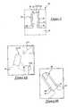
- FIGS. 2A and 2Bare enlarged, cross-sectional views illustrating the shapes of the silicon fins having square corners and rounded corners, respectively.
- FIG. 3is an enlarged, cross-sectional view illustrating an alternate embodiment of the present invention wherein the buried oxide layer under the silicon fins is undercut or notched by an etch process.
- FIGS. 4A and 4Bare illustrations of micrographs obtained in a cross-sectional transmission electron microscopy image.
- FIGS. 5A and 5Bare enlarged, plane views showing contact layouts for the present invention semiconductor structures.
- FIGS. 6A and 6Bare graphs illustrating drain current versus gate voltage curves for the present invention multiple-gate N-channel and P-channel MOSFETs, respectively.
- the present inventionrelates to the field of semiconductor devices and to the manufacture of field effect transistors with multiple-gates for scaling of the complementary metal-oxide-semiconductor (CMOS) technology well into the sub-50 nanometer (nm) regime.
- CMOScomplementary metal-oxide-semiconductor
- MOSFETMetal-oxide-semiconductor field effect transistor
- ULSIultra-large scale integrated circuits
- Reduction in the side of MOSFETshas provided continued improvement in speed performance, circuit density, and cost per unit function over the past few decades.
- the gate length of the MOSFETis reduced, the source and drain increasingly interact with the channel and gain influence on the channel potential. Consequently, a transistor with a short gate length suffers from problems related to the inability of the gate to substantially control the on and off states of the channel. Phenomena such as reduced gate control associated with transistors that have short channel lengths are termed short-channel effects.
- CMOS technologybeyond the limitations of the conventional bulk MOSFET and to realize the ultimate limit of silicon MOSFETs, a multiple-gate device structure should be used.
- the introduction of additional gatesimproves the capacitance coupling between the gates and the channel, increases the control of the channel potential by the gate, helps suppress short channel effects, and prolongs the scalability of the MOS transistor.
- a fabrication processthat overcomes the process difficulties faced in U.S. Pat. No. 6,413,802 is disclosed in which the use of an etchant mask after the fin formation process is eliminated.
- the process improvement to be described in the present invention methodresults in a multiple-gate structure that substantially wraps around a silicon fin or a transistor channel.
- the multiple-gate structureis superior in performance to those described in the prior art references.
- the fabrication processis superior or more manufacturable when compared to the prior art methods.
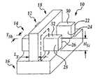
- FIGS. 1A, 1B and 1 CA process flow for fabricating the present invention multiple-gate structure 10 is schematically illustrated in FIGS. 1A, 1B and 1 C.
- the silicon fins 12 , 14are formed of a semi-conducting material, such as Si on top of an insulating material layer 16 , i.e., buried oxide, and patterned using an etchant mask (not shown).
- the etchant maskmay include a material commonly used for masking an etch process, such as photoresist, silicon oxide, silicon nitride, etc.
- the etchant maskis silicon oxide.
- an optional fin surface smoothing stepis used to improve or reduce the surface roughness of the fin sidewalls.
- the etchant mask used for fin definitionis silicon oxide, as in the preferred embodiment, it is removed either before or after the fin smoothing process.
- the removal of the etchant mask on the silicon fins 12 , 14 prior to gate dielectric 20 formationallows the device to have at least a triple-gate structure since the gate electrode 18 will finally be formed on each of the two sidewalls 22 , 24 , 26 , 28 as well as the top surfaces 30 , 32 of the fins 12 , 14 .
- the etchant mask used for fin definitionis a photoresist, it has to be removed before the fin surface smoothing step to avoid the high temperatures used in the fin smoothing process.
- the fin surface smoothingis performed by subjecting the fins 12 , 14 to a sacrificial oxidation and/or silicon sidewall treatment (e.g., high temperature anneal at 1000° C. in H 2 ambient).
- a sacrificial oxidation and/or silicon sidewall treatmente.g., high temperature anneal at 1000° C. in H 2 ambient.
- the surface smoothing of the fin sidewallscontributes to the achievement of good carrier mobilities.
- the shape of the finmay be square-like or rounded at the top. This is illustrated in FIGS. 2A and 2B.
- the buried oxide 16 under the silicon fins 12 , 14is undercut or notched by using an etch process.
- the etch processcan be a plasma etch or a wet etch using dilute hydroflouric acid (HF).
- HFdilute hydroflouric acid
- the undercut 40 (or notch) of the substrate insulating layer underlying the silicon fins 12 , 14allows the formation of an omega-shaped gate electrode 36 as depicted in FIG. 3.
- the featureallows additional capacitance coupling between the gate and the channel underneath the fin, and the structure thus emulates a wrap-around gate but avoids the process difficulties associated with the implementation of the wrap-around structure.
- the preceding descriptioncompletes the fin formation.
- the present invention processis followed by gate dielectric 38 formation.
- the gate dielectric 38may be formed by thermal oxidation, chemical vapor deposition, sputtering, etc.
- the thickness of the gate dielectricmay be different on the sidewalls 22 , 24 , 26 , 28 of the fin and the tops 30 , 32 of the fin.
- the gate dielectric thickness on the tops 30 , 32 of the finmay be thinner than the thickness on the fin sidewalls 22 , 24 , 26 , 28 .
- the gate dielectric thickness on the top surfaces 30 , 32 of the finis less than 20 ⁇ .
- the gate dielectricmay include a conventional material such as silicon dioxide or silicon oxynitride with a thickness ranging from 3 ⁇ to 100 ⁇ , preferably 10 ⁇ or less.
- the gate dielectricmay also include a high permittivity (high-k) material such as aluminum oxide Al 2 O 3 hafnium oxide HfO 2 , zirconium oxide ZrO 2 , with an equivalent oxide thickness of 3 ⁇ to 100 ⁇ .
- high-khigh permittivity
- the gate material 42is deposited.
- the gate materialmay be polycrystalline-silicon (poly-Si), poly-crystalline silicon germanium (poly-SiGe), a refractory metal such as molybdenum and tungsten, compounds such as titanium nitride, or other conducting materials.
- a gate mask(not shown) is defined and the underlying gate material 42 is etched to form the gate electrode 36 .
- the gate materialis poly-Si and the gate oxide is silicon oxynitride.
- a plasma etch using chlorine and bromine chemistrymay be used to achieve a high etch selectivity in excess of 2000 .
- a high etch selectivityis critical for device structures with a tall fin and aggressively scaled gate oxide thickness.
- the masking materialcan be removed.
- the lightly-doped drain (LDD) or drain extensionis formed next. This may be achieved by ion implantation, plasma immersion ion implantation (PIII), or other techniques known and used in the art.
- a spacer 48is formed on each of the sidewalls 44 , 46 of the gate 50 and the channel by deposition and selective etching of the spacer material.
- the spacer materialmay include a dielectric material such as silicon nitride or silicon dioxide as illustrated in FIG. 4B.
- the spacer 48is a silicon nitride/oxide composite spacer.
- source and drain regions(not shown) are doped by ion implantation, PIII, gas or solid source diffusion, or any other techniques known and used in the art. Any implant damage or amorphization can be annealed through subsequent exposure to elevated temperatures.
- the resistance of the source, drain, and gate 50can also be reduced by strapping the source, drain, and gate 50 with a conductive material.
- the conductive materialmay be a metallic silicide such as titanium silicide, cobalt silicide, or nickel silicide, a metallic nitride such as titanium nitride and tantalum nitride, a metal such as tungsten and copper, or a heavily doped semiconductor such as n+ doped Si.
- the conductive materialis cobalt silicide which may be formed by a self-aligned silicide (salicide) process.
- the cobalt-silicided poly-Si gateis shown in FIG. 4B.
- the conductive materialmay be formed on both the top of the fin as well as the sidewall of the fin.
- contactsare formed to the source, drain and gate regions using techniques known and used in the art. It is important to achieve a very low contact resistance in nanoscale devices.
- One way to reduce the contact resistanceis to increase the contact area by making contact with the fin sidewall.
- the contact layout (top view) shown in FIGS. 5A and 5Bmay be used.
- FIG. 6Athe drain current versus gate voltage of the multiple-gate N-channel and P-channel MOSFETs with gate lengths of 25 nm are shown.
- N+ and P+ dual poly-Si gatesare adopted for N- and P-channel MOSFETs, respectively.
- the drive currents for the N- and P-channel devicesare 1300 mA/ ⁇ m and 550 mA/ ⁇ m, respectively, as shown in FIG. 6B.
- in-situ doped N+ poly gatemay be used for both the N- and P-channel transistors.
Landscapes
- Thin Film Transistor (AREA)
- Insulated Gate Type Field-Effect Transistor (AREA)
- Metal-Oxide And Bipolar Metal-Oxide Semiconductor Integrated Circuits (AREA)
Abstract
Description
- The present invention generally relates to a multiple-gate transistor and method for fabricating and more particularly, relates to a multiple-gate semiconductor structure equipped with a gate electrode that wraps around a semiconductor fin on its top and sidewall surfaces separating a source and a drain region of the transistor and method for fabricating the structure.[0001]
- As the gate length of the MOSFET is scaled down into the sub-50 nm regime for improved performance and density, the requirements for body-doping concentration, gate oxide thickness, and source/drain (S/D) doping profiles to control short-channel effects become increasingly difficult to meet when conventional device structures based on bulk silicon (Si) substrates are employed. The heavy channel doping required to provide adequate suppression of short-channel effects results in degraded mobility a n d enhanced junction leakage. The aggressive reduction of the silicon dioxide SiO[0002]2gate dielectric thickness for reduced short-channel effects and improved drive current leads to increased direct tunneling gate leakage current and standby power consumption, and also raises concerns regarding the gate oxide reliability. For device scaling well into the sub-50 nm regime, a promising approach to controlling short-channel effects is to use an alternative device structure with multiple-gates, such as the double-gate and the surround-gate or wrap-around gate structure.
- A simple example of a multiple-gate device is the double-gate MOSFET structure, where there are two gate electrodes on the opposing sides of the channel. There are several ways in which a double-gate structure can be implemented. One way is the vertical-channel double-gate MOSFET. This is described by U.S. Pat. No. 6,372,559 B1 issued to Crowder et al. for a method of fabricating a self-aligned vertical double-gate MOSFET, and by U.S. Pat. No. 6,406,962 B1 issued to Agnello et al. for a vertical trench-formed dual-gate FET device structure and method for fabrication. A common feature of these two methods is that the source-to-drain direction is oriented normal to the plane of the substrate surface, and the gate-to-gate direction is parallel to the plane of the substrate surface. The device fabrication processes for such a double-gate structure are typically complicated, costly and suffer from poor manufacturability.[0003]
- Another method to fabricate a double-gate MOSFET is described by U.S. Pat. No. 6,413,802 B1 issued to Hu et al. for fin FET transistor structures having a double gate channel extending vertically from a substrate and methods for manufacture. In U.S. Pat. No. 6,413,802 B1, the device channel comprises a thin silicon fin formed on an insulative substrate (e.g., silicon oxide) and defined using an etchant mask. Gate oxidation is performed, followed by gate deposition and gate patterning to form a double-gate structure overlying the sides of the fin. Both the source-to-drain direction and the gate-to-gate direction are in the plane of the substrate surface. This device structure is widely recognized to be one of the most manufacturable double-gate structures. An integral feature of the double-gate MOSFET described in U.S. Pat. No. 6,413,802 B1 is the etchant mask on the silicon fin. The retention of the etchant mask is crucial due to problems faced in the etch process, particularly relating to the etch selectivity of the gate electrode with respect to the gate dielectric during the gate patterning step.[0004]
- It is therefore an object of the present invention to provide a multiple-gate transistor structure and a method for fabricating the structure that allows transistor scaling beyond the limits of the conventional bulk silicon MOSFET.[0005]
- In accordance with the present invention, a multiple-gate semiconductor structure and a method for fabricating the structure are provided.[0006]
- In a preferred embodiment, a multiple-gate semiconductor structure is provided which includes a substrate; source and drain islands formed in a portion of the substrate; a fin formed of a semi-conducting material having a top surface and two sidewall surfaces connecting the semiconductor source and drain islands; a gate dielectric layer overlying the fin; and a gate electrode wrapping around the fin on the top surface and the two sidewall surfaces of the fin separating the source and drain islands.[0007]
- In the multiple-gate semiconductor structure, the semiconducting material may be silicon, or may be silicon and germanium. The fin may be rounded at two top corners. The gate dielectric layer may include silicon oxide, silicon oxynitride, or a high permittivity material selected from the group consisting of La[0008]2O3, HfON, Al2O3, HfO2and ZrO2. The relative permittivity of the high permittivity material may be at least 5. The gate dielectric layer may have a thickness between 3 Å and 100 Å. The gate dielectric layer may have a first thickness on the fin sidewall surfaces and a second thickness on the fin top surface, wherein the first thickness is different from the second thickness. The second thickness may be smaller than the first thickness. The gate dielectric layer may have a thickness on the top surface of the fin less than 20 Å.
- The gate electrode may be formed of poly-crystalline silicon, or may be formed of poly-crystalline silicon germanium, or may be formed of a metal. The source and drain islands each may include a lightly doped or extension region. The source and drain islands may be strapped by a conductive material selected from the group consisting of metals and suicides. Contacts between the conductive material and the source and drain islands are made on at least one of the sidewall and top surfaces of the fin.[0009]
- The present invention is further directed to a multiple-gate semiconductor structure that includes a substrate that has a depression in a top surface, the depression includes an undercut or a notch; a fin formed of a semi-conducting material and has a top surface and two sidewall surfaces, the fin is positioned vertically juxtaposed to the depression in the top surface of the substrate; source and drain regions formed in the semi-conducting material of the fin; a gate dielectric layer overlying the fin; and a gate electrode wrapping around the fin on the two sidewall surfaces, the top surface and a bottom of a base of the fin separating the source and drain regions.[0010]
- In the multiple-gate semiconductor structure, the semiconducting material may include silicon, or may include silicon and germanium. The fin may be rounded at two top corners, or may have two square corners. The gate dielectric layer may include silicon oxide, may include silicon oxynitride, or may include a high permittivity material selected from the group consisting of La[0011]2O3, HfON, Al2O3, HfO2and ZrO2. The relative permittivity may be at least 5. The gate dielectric layer may have a thickness between 3 Å and 100 Å. The gate dielectric layer may have a first thickness on the fin sidewall surfaces and a second thickness on the fin top surface, wherein the first thickness may be different from the second thickness. The second thickness may be smaller than the first thickness. The gate dielectric layer may have a thickness on the top surface of the fin less than 20 Å.
- In the multiple-gate semiconductor structure, the gate electrode may include poly-crystalline silicon, may include poly-crystalline silicon germanium, or may include a metal. The source and drain islands may each include a lightly doped or extension region. The source and drain islands may be strapped by a conductive material selected from the group consisting of metals and silicides. Contacts between the conductive material and the source and drain islands may be made on at least one of the sidewall and top surfaces of the fin.[0012]
- The present invention is still further directed to a method for fabricating a multiple-gate semiconductor structure which includes the steps of providing a substrate that includes a semi-conducting layer overlying an insulating layer; patterning and forming a fin in the semi-conducting layer, the fin has two sidewall surfaces and a top surface; depositing a layer of a dielectric material overlying the fin; depositing a layer of a conductive material overlying the layer of dielectric material; patterning the layer of conductive material forming a gate straddling across the two sidewall surfaces and the top surface of the fin; and forming a source and a drain region in the semi-conducting layer.[0013]
- The method for fabricating a multiple-gate semiconductor structure may further include the step of forming the semi-conducting substrate in a material including silicon, or in a material including silicon and germanium. The method may further include the step of forming the layer of dielectric material in silicon oxide. The fin forming process may further include a fin surface smoothing step, wherein the fin surface smoothing step may further include sub-steps of sacrificial oxidation and high temperature annealing in a hydrogen ambient. The method may further include the step of forming the dielectric layer in a material including silicon oxide, or silicon oxynitride, or a high permittivity material selected from the group consisting of La[0014]2O3, HfON, Al2O3, HfO2and ZrO2. The high permittivity material may have a relative permittivity of at least 5.
- The method may further include the step of forming the gate dielectric layer to a thickness between 3 Å and 100 Å. The method may further include the step of forming a different thickness of the dielectric layer on the sidewall surfaces and on the top surface of the fin, or the step of forming the gate dielectric layer to a smaller thickness on the top surface of the fin compared to the gate dielectric layer on the sidewall surfaces of the fin. The method may further include the step of forming the gate dielectric layer on the top surface of the fin to a thickness of less than 20 Å. The method may further include the step of forming the gate in a material including poly-crystalline silicon, or poly-crystalline silicon germanium. The method may further include the step of forming the source or drain region in a lightly doped or extension region. The method may further include the step of forming a layer of a conductive material on top of the source and drain regions, or forming the layer of conductive material in a material selected from the group consisting of metal, metallic silicide and metallic nitride.[0015]
- The present invention is still further directed to a method for fabricating a multiple-gate semiconductor structure that include the steps of providing a substrate that includes a semi-conducting layer overlying an insulating layer; patterning and forming a fin in the semi-conducting layer, the fin has two sidewall surfaces and a top surface; forming a depression in a top surface of the substrate at a base of the fin; depositing a layer of a dielectric material overlying the fin; depositing a layer of a conductive material overlying the layer of dielectric material; patterning the layer of conductive material forming a gate straddling across the two sidewall surfaces and the top surface of the fin; and forming a source and a drain region in the semi-conducting layer.[0016]
- The method for fabricating a multiple-gate semiconductor structure may further include the step of forming the depression in the top surface of the substrate by undercutting at the base of the fin, or the step of forming the depression by undercutting using an etch process. The method may further include the step of forming a layer of a conductive material on top of the source and drain regions, or forming the layer of conductive material selected from the group consisting of metal, metallic silicide and metallic nitride.[0017]
- These and other objects, features and advantages of the present invention will become apparent from the following detailed description and the appended drawings in which:[0018]
- FIGS. 1A, 1B and[0019]1C are enlarged, perspective views illustrating a fabrication process for the present invention multiple-gate structure wherein two silicon fins are patterned and formed on a substrate with an insulating layer inbetween the fins and the substrate.
- FIGS. 2A and 2B are enlarged, cross-sectional views illustrating the shapes of the silicon fins having square corners and rounded corners, respectively.[0020]
- FIG. 3 is an enlarged, cross-sectional view illustrating an alternate embodiment of the present invention wherein the buried oxide layer under the silicon fins is undercut or notched by an etch process.[0021]
- FIGS. 4A and 4B are illustrations of micrographs obtained in a cross-sectional transmission electron microscopy image.[0022]
- FIGS. 5A and 5B are enlarged, plane views showing contact layouts for the present invention semiconductor structures.[0023]
- FIGS. 6A and 6B are graphs illustrating drain current versus gate voltage curves for the present invention multiple-gate N-channel and P-channel MOSFETs, respectively.[0024]
- The present invention relates to the field of semiconductor devices and to the manufacture of field effect transistors with multiple-gates for scaling of the complementary metal-oxide-semiconductor (CMOS) technology well into the sub-50 nanometer (nm) regime.[0025]
- Metal-oxide-semiconductor field effect transistor (MOSFET) technology is the dominant semiconductor technology used for the manufacture of ultra-large scale integrated (ULSI) circuits. Reduction in the side of MOSFETs has provided continued improvement in speed performance, circuit density, and cost per unit function over the past few decades. As the gate length of the MOSFET is reduced, the source and drain increasingly interact with the channel and gain influence on the channel potential. Consequently, a transistor with a short gate length suffers from problems related to the inability of the gate to substantially control the on and off states of the channel. Phenomena such as reduced gate control associated with transistors that have short channel lengths are termed short-channel effects. Increased body doping concentration, reduced gate oxide thickness, and ultra-shallow source/drain junctions are ways to suppress short-channel effects. However, for device scaling well into the sub-50 nm regime, the requirements for body-doping concentration, gate oxide thickness, and source/drain (S/D) doping profiles become increasingly difficult to meet when conventional device structures based on bulk silicon (Si) substrates are employed. The heavy channel doping required to provide adequate suppression of short-channel effects results in degraded mobility and enhanced junction leakage. The aggressive reduction of the silicon dioxide SiO[0026]2gate dielectric thickness for reduced short-channel effects and improved drive current leads to increased direct tunneling gate leakage current and standby power consumption, and also raises concerns regarding the gate oxide reliability. Innovations in front-end process technologies or the introduction of alternative device structures are required to sustain the historical pace of scaling.
- To extend the scalability of CMOS technology beyond the limitations of the conventional bulk MOSFET and to realize the ultimate limit of silicon MOSFETs, a multiple-gate device structure should be used. The introduction of additional gates improves the capacitance coupling between the gates and the channel, increases the control of the channel potential by the gate, helps suppress short channel effects, and prolongs the scalability of the MOS transistor.[0027]
- In the present invention, a fabrication process that overcomes the process difficulties faced in U.S. Pat. No. 6,413,802 is disclosed in which the use of an etchant mask after the fin formation process is eliminated. In addition, the process improvement to be described in the present invention method results in a multiple-gate structure that substantially wraps around a silicon fin or a transistor channel. The multiple-gate structure is superior in performance to those described in the prior art references. Moreover, the fabrication process is superior or more manufacturable when compared to the prior art methods.[0028]
- A process flow for fabricating the present invention[0029]
multiple-gate structure 10 is schematically illustrated in FIGS. 1A, 1B and1C. Thesilicon fins material layer 16, i.e., buried oxide, and patterned using an etchant mask (not shown). The etchant mask may include a material commonly used for masking an etch process, such as photoresist, silicon oxide, silicon nitride, etc. In a preferred embodiment, the etchant mask is silicon oxide. In the present invention method, an optional fin surface smoothing step is used to improve or reduce the surface roughness of the fin sidewalls. When the etchant mask used for fin definition is silicon oxide, as in the preferred embodiment, it is removed either before or after the fin smoothing process. The removal of the etchant mask on thesilicon fins gate dielectric 20 formation allows the device to have at least a triple-gate structure since thegate electrode 18 will finally be formed on each of the twosidewalls top surfaces fins fins - In an alternate embodiment, the buried[0030]
oxide 16 under thesilicon fins silicon fins gate electrode 36 as depicted in FIG. 3. The feature allows additional capacitance coupling between the gate and the channel underneath the fin, and the structure thus emulates a wrap-around gate but avoids the process difficulties associated with the implementation of the wrap-around structure. The preceding description completes the fin formation. - The present invention process is followed by[0031]
gate dielectric 38 formation. Thegate dielectric 38 may be formed by thermal oxidation, chemical vapor deposition, sputtering, etc. In general, the thickness of the gate dielectric may be different on thesidewalls top surfaces silicon fin - Next, the[0032]
gate material 42 is deposited. The gate material may be polycrystalline-silicon (poly-Si), poly-crystalline silicon germanium (poly-SiGe), a refractory metal such as molybdenum and tungsten, compounds such as titanium nitride, or other conducting materials. A gate mask (not shown) is defined and theunderlying gate material 42 is etched to form thegate electrode 36. The gate etch stops on the gate oxide, and the gate is electrically isolated from the transistor structure by the gate oxide. In the preferred embodiment, the gate material is poly-Si and the gate oxide is silicon oxynitride. A plasma etch using chlorine and bromine chemistry may be used to achieve a high etch selectivity in excess of2000. A high etch selectivity is critical for device structures with a tall fin and aggressively scaled gate oxide thickness. After the definition of thegate 50, the masking material can be removed. The lightly-doped drain (LDD) or drain extension is formed next. This may be achieved by ion implantation, plasma immersion ion implantation (PIII), or other techniques known and used in the art. Next, aspacer 48 is formed on each of thesidewalls gate 50 and the channel by deposition and selective etching of the spacer material. The spacer material may include a dielectric material such as silicon nitride or silicon dioxide as illustrated in FIG. 4B. - In the preferred embodiment, the[0033]
spacer 48 is a silicon nitride/oxide composite spacer. After spacer48 formation, source and drain regions (not shown) are doped by ion implantation, PIII, gas or solid source diffusion, or any other techniques known and used in the art. Any implant damage or amorphization can be annealed through subsequent exposure to elevated temperatures. The resistance of the source, drain, andgate 50 can also be reduced by strapping the source, drain, andgate 50 with a conductive material. The conductive material may be a metallic silicide such as titanium silicide, cobalt silicide, or nickel silicide, a metallic nitride such as titanium nitride and tantalum nitride, a metal such as tungsten and copper, or a heavily doped semiconductor such as n+ doped Si. In the preferred embodiment, the conductive material is cobalt silicide which may be formed by a self-aligned silicide (salicide) process. The cobalt-silicided poly-Si gate is shown in FIG. 4B. In the source and drain regions, the conductive material may be formed on both the top of the fin as well as the sidewall of the fin. - Next, contacts are formed to the source, drain and gate regions using techniques known and used in the art. It is important to achieve a very low contact resistance in nanoscale devices. One way to reduce the contact resistance is to increase the contact area by making contact with the fin sidewall. The contact layout (top view) shown in FIGS. 5A and 5B may be used.[0034]
- In FIG. 6A, the drain current versus gate voltage of the multiple-gate N-channel and P-channel MOSFETs with gate lengths of 25 nm are shown. N+ and P+ dual poly-Si gates are adopted for N- and P-channel MOSFETs, respectively. At a supply voltage of 0.7 V, the drive currents for the N- and P-channel devices are 1300 mA/μm and 550 mA/μm, respectively, as shown in FIG. 6B. For a supply voltage of 1 V, in-situ doped N+ poly gate may be used for both the N- and P-channel transistors.[0035]
- While the present invention has been described in an illustrative manner, it should be understood that the terminology used is intended to be in a nature of words of description rather than of limitation.[0036]
- Furthermore, while the present invention has been described in terms of a preferred and an alternate embodiment, it is to be appreciated that those skilled in the art will readily apply these teachings to other possible variations of the inventions.[0037]
- The embodiment of the invention in which an exclusive property or privilege is claimed are defined as follows.[0038]
Claims (76)
1. A multiple-gate semiconductor structure comprising:
a substrate;
source and drain islands formed in a portion of said substrate;
a fin formed of a semi-conducting material having a top surface and two sidewall surfaces;
a gate dielectric layer overlying said fin; and
a gate electrode wrapping around said fin on said top surface and said two sidewall surfaces separating source and drain islands.
2. The multiple-gate semiconductor structure ofclaim 1 , wherein said semi-conducting material comprises silicon.
3. The multiple-gate semiconductor structure ofclaim 1 , wherein said semi-conducting material comprises silicon and germanium.
4. The multiple-gate semiconductor structure ofclaim 1 , wherein said fin is rounded at two top corners.
5. The multiple-gate semiconductor structure ofclaim 1 , wherein said gate dielectric layer comprises silicon oxide.
6. The multiple-gate semiconductor structure ofclaim 1 , wherein said gate dielectric layer comprises silicon oxynitride.
7. The multiple-gate semiconductor structure ofclaim 1 , wherein said gate dielectric layer comprises a high permittivity material selected from the group consisting of La2O3, HfON, Al2O3, HfO2and ZrO2.
8. The multiple-gate semiconductor structure ofclaim 1 , wherein said high permittivity material having a relative permittivity of at least 5.
9. The multiple-gate semiconductor structure ofclaim 1 , wherein said gate dielectric layer having a thickness between 3 Å and 100 Å.
10. The multiple-gate semiconductor structure ofclaim 1 , wherein said gate dielectric layer having a first thickness on said fin sidewall surfaces and a second thickness on said fin top surface, said first thickness being different from said second thickness.
11. The multiple-gate semiconductor structure ofclaim 1 , wherein said second thickness is smaller than said first thickness.
12. The multiple-gate semiconductor structure ofclaim 1 , wherein said gate dielectric layer having a thickness on the top surface of said fin less than 20 Å.
13. The multiple-gate semiconductor structure ofclaim 1 , wherein said gate electrode comprises poly-crystalline silicon.
14. The multiple-gate semiconductor structure ofclaim 1 , wherein said gate electrode comprises poly-crystalline silicon germanium.
15. The multiple-gate semiconductor structure ofclaim 1 , wherein said gate electrode comprises a metal.
16. The multiple-gate semiconductor structure ofclaim 1 , wherein said source and drain islands each comprises a lightly doped or extension region.
17. The multiple-gate semiconductor structure ofclaim 1 , wherein said source and drain islands are strapped by a conductive material selected from the group consisting of metals and silicides.
18. The multiple-gate semiconductor structure ofclaim 17 , wherein contacts between said conductive material and said source and drain islands are on at least one of the sidewall and top surfaces of the fin.
19. A multiple-gate semiconductor structure comprising of:
a substrate having a depression in a top surface, said depression comprises an undercut or a notch;
a fin formed of a semi-conducting material having a top surface and two sidewall surfaces, said fin being positioned vertically juxtaposed to said depression in said top surface of the substrate;
source and drain regions formed in said semi-conducting material of said fin;
a gate dielectric layer overlying said fin; and
a gate electrode wrapping around said fin on said two sidewall surfaces, said top surface, and a bottom of a base of said fin separating said source and drain regions.
20. The multiple-gate semiconductor structure ofclaim 19 , wherein said semi-conducting material comprises silicon.
21. The multiple-gate semiconductor structure ofclaim 19 , wherein said semi-conducting material comprises silicon and germanium.
22. The multiple-gate semiconductor structure ofclaim 19 , wherein said fin is rounded at two top corners.
23. The multiple-gate semiconductor structure ofclaim 19 , wherein said gate dielectric layer comprises silicon oxide.
24. The multiple-gate semiconductor structure ofclaim 19 , wherein said gate dielectric layer comprises silicon oxynitride.
25. The multiple-gate semiconductor structure ofclaim 19 , wherein said gate dielectric layer comprises a high permittivity material selected from the group consisting of La2O3, HfON, Al2O3, HfO2and ZrO2.
26. The multiple-gate semiconductor structure ofclaim 25 , wherein said high permittivity material having a relative permittivity of at least 5.
27. The multiple-gate semiconductor structure ofclaim 19 , wherein said gate dielectric layer having a thickness between 3 Å and 100 Å.
28. The multiple-gate semiconductor structure ofclaim 19 , wherein said gate dielectric layer having a first thickness on said fin sidewall surfaces and a second thickness on said fin top surface, said first thickness being different from said second thickness.
29. The multiple-gate semiconductor structure ofclaim 19 , wherein said second thickness is smaller than said first thickness.
30. The multiple-gate semiconductor structure ofclaim 19 , wherein said gate dielectric layer having a thickness on the top surface of said fin less than 20 Å.
31. The multiple-gate semiconductor structure ofclaim 19 , wherein said gate electrode comprises poly-crystalline silicon.
32. The multiple-gate semiconductor structure ofclaim 19 , wherein said gate electrode comprises poly-crystalline silicon germanium.
33. The multiple-gate semiconductor structure ofclaim 19 , wherein said gate electrode comprises a metal.
34. The multiple-gate semiconductor structure ofclaim 19 , wherein said source and drain islands each comprises a lightly doped or extension region.
35. The multiple-gate semiconductor structure ofclaim 19 , wherein said source and drain islands are strapped by a conductive material selected from the group consisting of metals and suicides.
36. The multiple-gate semiconductor structure ofclaim 19 , wherein contacts between said conductive material and said source and drain islands are on at least one of the sidewall and top surfaces of the fin.
37. A method for fabricating a multiple-gate semiconductor structure comprising the steps of:
providing a substrate comprising a semi-conducting layer overlying an insulating layer;
patterning and forming a fin in said semi-conducting layer, said fin having two sidewall surfaces and a top surface;
depositing a layer of a dielectric material overlying said fin;
depositing a layer of a conductive material overlying said layer of dielectric material;
patterning said layer of conductive material forming a gate straddling across said two sidewall surfaces and said top surface of the fin; and
forming a source and drain region in said semi-conducting layer.
38. The method ofclaim 37 further comprising the step of forming said semi-conducting layer in a material comprising silicon.
39. The method ofclaim 37 further comprising the step of forming said semi-conducting layer in a material comprising silicon and germanium.
40. The method ofclaim 37 further comprising the step of forming said layer of dielectric material in a material comprising silicon oxide.
41. The method ofclaim 37 , wherein said fin forming step further comprising a fin surface smoothing step.
42. The method ofclaim 41 , wherein said fin surface smoothing step further comprising sub-steps of sacrificial oxidation and high temperature annealing in a hydrogen ambient.
43. The method ofclaim 37 , further comprising the step of forming said dielectric layer in a material comprising silicon oxide.
44. The method ofclaim 37 , further comprising the step of forming said gate dielectric layer in a material comprising silicon oxynitride.
45. The method ofclaim 37 , further comprising the step of forming said gate dielectric layer in a high permittivity material selected from the group consisting of La2O3, HfON, Al2O3, HfO2and ZrO2.
46. The method ofclaim 45 , wherein said high permittivity material has a relative permittivity of at least 5.
47. The method ofclaim 37 , further comprising the step of forming said gate dielectric layer to a thickness between 3 Å and 100 Å.
48. The method ofclaim 37 , further comprising the step of forming a different thickness of said dielectric layer on the sidewall surfaces and on the top surface of the fin.
49. The method ofclaim 37 , further comprising the step of forming said gate dielectric layer to a smaller thickness on the top surface of the fin compared to the gate dielectric layer on the sidewall surfaces of the fin.
50. The method ofclaim 37 , further comprising the step of forming the gate dielectric layer on the top surface of the fin to a thickness of less than 20 Å.
51. The method ofclaim 37 , further comprising the step of forming said gate in a material comprising poly-crystalline silicon.
52. The method ofclaim 37 , further comprising the step of forming said gate in a material comprising polysilicon germanium.
53. The method ofclaim 37 , further comprising the step of forming said source or drain region in a lightly doped or extension region.
54. The method ofclaim 37 , further comprising the step of forming a layer of a conductive material on top of said source and drain regions.
55. The method ofclaim 54 , further comprising the step of forming said layer of conductive material in a material selected from the group consisting of metal, metallic silicide and metallic nitride.
56. A method for fabricating a multiple-gate semiconductor structure comprising the steps of:
providing a substrate comprising of a semi-conducting layer overlying an insulating layer;
patterning and forming a fin in said semi-conducting layer, said fin having two sidewall surfaces and a top surface;
forming a depression in a top surface of the substrate at a base of said fin;
depositing a layer of a dielectric material overlying said fin;
depositing a layer of a conductive material overlying said layer of dielectric material;
patterning said layer of conductive material forming a gate straddling across said two sidewall surfaces and said top surface of the fin; and
forming a source and a drain region in said semi-conducting layer.
57. The method for fabricating a multiple-gate semiconductor structure according toclaim 56 , further comprising the step of forming said semi-conducting layer in a material comprising silicon.
58. The method for fabricating a multiple-gate semiconductor structure according toclaim 56 , further comprising the step of forming said semi-conducting layer in a material comprising silicon and germanium.
59. The method for fabricating a multiple-gate semiconductor structure according toclaim 56 , further comprising the step of forming said layer of dielectric material in a material comprising silicon oxide.
60. The method for fabricating a multiple-gate semiconductor structure according toclaim 56 , wherein said fin forming step further comprises a fin surface smoothing step.
61. The method for fabricating a multiple-gate semiconductor structure according toclaim 60 , wherein said fin surface smoothing step further comprises sub-steps all sacrificial oxidation and high temperature annealing in a hydrogen ambient.
62. The method for fabricating a multiple-gate semiconductor structure according toclaim 56 , further comprising the step of forming said depression in said top surface of the substrate by undercutting at the base of the fin.
63. The method for fabricating a multiple-gate semiconductor structure according toclaim 62 , further comprising the step of forming said depression by undercutting using an etch process.
64. The method for fabricating a multiple-gate semiconductor structure according toclaim 56 , further comprising the step of forming said gate dielectric layer in a material comprising silicon oxide.
65. The method for fabricating a multiple-gate semiconductor structure according toclaim 56 , further comprising the step of forming said gate dielectric layer in a material comprising silicon oxynitride.
66. The method for fabricating a multiple-gate semiconductor structure according toclaim 56 , further comprising the step of forming said gate dielectric layer in a high permittivity material selected from the group consisting of La2O3, HfON, Al2O3, HfO2and ZrO2.
67. The method for fabricating a multiple-gate semiconductor structure according toclaim 66 , wherein said high permittivity material has a relative permittivity of at least 5.
68. The method for fabricating a multiple-gate semiconductor structure according toclaim 56 , further comprising the step of forming said gate dielectric layer to a thickness between 3 Å and 100 Å.
69. The method for fabricating a multiple-gate semiconductor structure according toclaim 56 , further comprising the step of forming a different thickness of the gate dielectric layer on the sidewall surfaces and on the top surface of the fin.
70. The method for fabricating a multiple-gate semiconductor structure according toclaim 56 , further comprising the step of forming said gate dielectric layer to a smaller thickness on the top surface of the fin compared to the gate dielectric layer on the sidewall surfaces of the fin.
71. The method for fabricating a multiple-gate semiconductor structure according toclaim 56 , further comprising the step of forming the gate dielectric layer on the top surface of the fin to a thickness of less than 20 Å.
72. The method for fabricating a multiple-gate semiconductor structure according toclaim 56 , further comprising the step of forming said gate in a material comprising poly-crystalline silicon.
73. The method for fabricating a multiple-gate semiconductor structure according toclaim 56 , further comprising the step of forming said gate in a material comprising polysilicon germanium.
74. The method for fabricating a multiple-gate semiconductor structure according toclaim 56 , further comprising the step of forming said source and drain region in a lightly doped or extension region.
75. The method for fabricating a multiple-gate semiconductor structure according toclaim 56 , further comprising the step of forming a layer of a conductive material on top of said source and drain regions.
76. The method for fabricating a multiple-gate semiconductor structure according toclaim 75 , further comprising the step of forming said layer of conductive material in a material selected from the group consisting of metal, metallic silicide and metallic nitride.
Priority Applications (4)
| Application Number | Priority Date | Filing Date | Title |
|---|---|---|---|
| US10/314,249US7728360B2 (en) | 2002-12-06 | 2002-12-06 | Multiple-gate transistor structure |
| SG200305885ASG123567A1 (en) | 2002-12-06 | 2003-10-03 | Multiple-gate transistor structure and method for fabricating |
| CN200310101713.9ACN1264217C (en) | 2002-12-06 | 2003-10-21 | Multiple gate structure and manufacturing method thereof |
| US12/758,953US7948037B2 (en) | 2002-12-06 | 2010-04-13 | Multiple-gate transistor structure and method for fabricating |
Applications Claiming Priority (1)
| Application Number | Priority Date | Filing Date | Title |
|---|---|---|---|
| US10/314,249US7728360B2 (en) | 2002-12-06 | 2002-12-06 | Multiple-gate transistor structure |
Related Child Applications (1)
| Application Number | Title | Priority Date | Filing Date |
|---|---|---|---|
| US12/758,953DivisionUS7948037B2 (en) | 2002-12-06 | 2010-04-13 | Multiple-gate transistor structure and method for fabricating |
Publications (2)
| Publication Number | Publication Date |
|---|---|
| US20040108523A1true US20040108523A1 (en) | 2004-06-10 |
| US7728360B2 US7728360B2 (en) | 2010-06-01 |
Family
ID=32468442
Family Applications (2)
| Application Number | Title | Priority Date | Filing Date |
|---|---|---|---|
| US10/314,249Active2026-05-29US7728360B2 (en) | 2002-12-06 | 2002-12-06 | Multiple-gate transistor structure |
| US12/758,953Expired - Fee RelatedUS7948037B2 (en) | 2002-12-06 | 2010-04-13 | Multiple-gate transistor structure and method for fabricating |
Family Applications After (1)
| Application Number | Title | Priority Date | Filing Date |
|---|---|---|---|
| US12/758,953Expired - Fee RelatedUS7948037B2 (en) | 2002-12-06 | 2010-04-13 | Multiple-gate transistor structure and method for fabricating |
Country Status (3)
| Country | Link |
|---|---|
| US (2) | US7728360B2 (en) |
| CN (1) | CN1264217C (en) |
| SG (1) | SG123567A1 (en) |
Cited By (42)
| Publication number | Priority date | Publication date | Assignee | Title |
|---|---|---|---|---|
| US20040157396A1 (en)* | 2003-02-10 | 2004-08-12 | Byeong-Chan Lee | Methods for forming double gate electrodes using tunnel and trench |
| US20050158970A1 (en)* | 2004-01-16 | 2005-07-21 | Robert Chau | Tri-gate transistors and methods to fabricate same |
| US6960509B1 (en)* | 2004-06-30 | 2005-11-01 | Freescale Semiconductor, Inc. | Method of fabricating three dimensional gate structure using oxygen diffusion |
| US20050275010A1 (en)* | 2004-06-10 | 2005-12-15 | Hung-Wei Chen | Semiconductor nano-wire devices and methods of fabrication |
| KR100593369B1 (en) | 2004-09-23 | 2006-06-28 | 한국과학기술원 | Method for fabricating multi-gate field effect transistor using round silicon nanowires and its structure |
| US20060220133A1 (en)* | 2003-04-29 | 2006-10-05 | Yee-Chia Yeo | Doping of semiconductor fin devices |
| WO2007005697A3 (en)* | 2005-06-30 | 2007-04-12 | Intel Corp | Block contact architectures for nanoscale channel transistors |
| US20070152266A1 (en)* | 2005-12-29 | 2007-07-05 | Intel Corporation | Method and structure for reducing the external resistance of a three-dimensional transistor through use of epitaxial layers |
| US7456476B2 (en) | 2003-06-27 | 2008-11-25 | Intel Corporation | Nonplanar semiconductor device with partially or fully wrapped around gate electrode and methods of fabrication |
| US20080296702A1 (en)* | 2007-05-30 | 2008-12-04 | Tsung-Lin Lee | Integrated circuit structures with multiple FinFETs |
| US7479421B2 (en) | 2005-09-28 | 2009-01-20 | Intel Corporation | Process for integrating planar and non-planar CMOS transistors on a bulk substrate and article made thereby |
| US20090127625A1 (en)* | 2007-11-21 | 2009-05-21 | Kabushiki Kaisha Toshiba | Semiconductor device |
| US20090149012A1 (en)* | 2004-09-30 | 2009-06-11 | Brask Justin K | Method of forming a nonplanar transistor with sidewall spacers |
| US7547637B2 (en) | 2005-06-21 | 2009-06-16 | Intel Corporation | Methods for patterning a semiconductor film |
| US20090194802A1 (en)* | 2006-05-17 | 2009-08-06 | Mark Fischer | Semiconductor Constructions, and DRAM Arrays |
| US20090269918A1 (en)* | 2008-04-28 | 2009-10-29 | Yi Ma | Methods for fabricating memory cells having fin structures with smoot sidewalls and rounded top corners and edges |
| US7736956B2 (en) | 2005-08-17 | 2010-06-15 | Intel Corporation | Lateral undercut of metal gate in SOI device |
| US7781771B2 (en) | 2004-03-31 | 2010-08-24 | Intel Corporation | Bulk non-planar transistor having strained enhanced mobility and methods of fabrication |
| US7879675B2 (en) | 2005-03-14 | 2011-02-01 | Intel Corporation | Field effect transistor with metal source/drain regions |
| US7902014B2 (en) | 2005-09-28 | 2011-03-08 | Intel Corporation | CMOS devices with a single work function gate electrode and method of fabrication |
| US7960794B2 (en) | 2004-08-10 | 2011-06-14 | Intel Corporation | Non-planar pMOS structure with a strained channel region and an integrated strained CMOS flow |
| US7989280B2 (en) | 2005-11-30 | 2011-08-02 | Intel Corporation | Dielectric interface for group III-V semiconductor device |
| US8067818B2 (en) | 2004-10-25 | 2011-11-29 | Intel Corporation | Nonplanar device with thinned lower body portion and method of fabrication |
| US8084818B2 (en) | 2004-06-30 | 2011-12-27 | Intel Corporation | High mobility tri-gate devices and methods of fabrication |
| US8183646B2 (en) | 2005-02-23 | 2012-05-22 | Intel Corporation | Field effect transistor with narrow bandgap source and drain regions and method of fabrication |
| US8268709B2 (en) | 2004-09-29 | 2012-09-18 | Intel Corporation | Independently accessed double-gate and tri-gate transistors in same process flow |
| US8362566B2 (en) | 2008-06-23 | 2013-01-29 | Intel Corporation | Stress in trigate devices using complimentary gate fill materials |
| US8405164B2 (en) | 2003-06-27 | 2013-03-26 | Intel Corporation | Tri-gate transistor device with stress incorporation layer and method of fabrication |
| TWI416722B (en)* | 2008-12-05 | 2013-11-21 | Micron Technology Inc | Semiconductor device structure and related method including a transistor having energy shielding adjacent to a transistor channel |
| US8617945B2 (en) | 2006-08-02 | 2013-12-31 | Intel Corporation | Stacking fault and twin blocking barrier for integrating III-V on Si |
| US8716803B2 (en)* | 2012-10-04 | 2014-05-06 | Flashsilicon Incorporation | 3-D single floating gate non-volatile memory device |
| US20140183643A1 (en)* | 2012-12-28 | 2014-07-03 | Taiwan Semiconductor Manufacturing Company, Ltd. | Transistors with Wrapped-Around Gates and Methods for Forming the Same |
| US8791506B2 (en) | 2006-08-28 | 2014-07-29 | Micron Technology, Inc. | Semiconductor devices, assemblies and constructions |
| US20140306274A1 (en)* | 2013-04-11 | 2014-10-16 | International Business Machines Corporation | SELF-ALIGNED STRUCTURE FOR BULK FinFET |
| US20140370667A1 (en)* | 2012-02-09 | 2014-12-18 | International Business Machines Corporation | Tapered nanowire structure with reduced off current |
| CN104347721A (en)* | 2013-08-07 | 2015-02-11 | 英飞凌科技德累斯顿有限责任公司 | Power transistor |
| US20150228781A1 (en)* | 2014-02-07 | 2015-08-13 | Globalfoundries Inc. | Method for making semiconductor device with stressed semiconductor and related devices |
| US9263455B2 (en) | 2013-07-23 | 2016-02-16 | Micron Technology, Inc. | Methods of forming an array of conductive lines and methods of forming an array of recessed access gate lines |
| US9337307B2 (en) | 2005-06-15 | 2016-05-10 | Intel Corporation | Method for fabricating transistor with thinned channel |
| US9349850B2 (en) | 2013-07-17 | 2016-05-24 | Taiwan Semiconductor Manufacturing Company, Ltd. | Thermally tuning strain in semiconductor devices |
| US9419098B2 (en) | 2013-05-30 | 2016-08-16 | Taiwan Semiconductor Manufacturing Company, Ltd. | Tuning strain in semiconductor devices |
| US20230135321A1 (en)* | 2021-11-03 | 2023-05-04 | International Business Machines Corporation | Integrated short channel omega gate finfet and long channel finfet |
Families Citing this family (17)
| Publication number | Priority date | Publication date | Assignee | Title |
|---|---|---|---|---|
| US7728360B2 (en)* | 2002-12-06 | 2010-06-01 | Taiwan Semiconductor Manufacturing Co., Ltd. | Multiple-gate transistor structure |
| US7838345B2 (en)* | 2006-05-02 | 2010-11-23 | Freescale Semiconductor, Inc. | Electronic device including semiconductor fins and a process for forming the electronic device |
| US7691690B2 (en)* | 2007-01-12 | 2010-04-06 | International Business Machines Corporation | Methods for forming dual fully silicided gates over fins of FinFet devices |
| US8420456B2 (en) | 2007-06-12 | 2013-04-16 | Semiconductor Energy Laboratory Co., Ltd. | Method of manufacturing for thin film transistor |
| US20090020792A1 (en)* | 2007-07-18 | 2009-01-22 | Rafael Rios | Isolated tri-gate transistor fabricated on bulk substrate |
| US8124507B2 (en)* | 2009-06-24 | 2012-02-28 | Panasonic Corporation | Semiconductor device and method for fabricating the same |
| US8395195B2 (en)* | 2010-02-09 | 2013-03-12 | Taiwan Semiconductor Manufacturing Company, Ltd. | Bottom-notched SiGe FinFET formation using condensation |
| US8361884B2 (en)* | 2010-06-22 | 2013-01-29 | Infineon Technologies Ag | Plasma dicing and semiconductor devices formed thereof |
| CN102969248B (en)* | 2011-09-01 | 2015-06-17 | 中芯国际集成电路制造(上海)有限公司 | Manufacturing method for fin type field effect transistor |
| CN104160507B (en)* | 2011-12-28 | 2017-10-24 | 英特尔公司 | Method for Integrating Multiple Gate Dielectric Transistors on a Tri-Gate (FINFET) Process |
| US8956942B2 (en)* | 2012-12-21 | 2015-02-17 | Stmicroelectronics, Inc. | Method of forming a fully substrate-isolated FinFET transistor |
| US9524986B2 (en) | 2014-06-26 | 2016-12-20 | Globalfoundries Inc. | Trapping dislocations in high-mobility fins below isolation layer |
| TWI553869B (en)* | 2014-07-31 | 2016-10-11 | 瑞昱半導體股份有限公司 | Semiconductor component and multi-gate field effect transistor |
| TWI655774B (en) | 2015-08-12 | 2019-04-01 | 聯華電子股份有限公司 | Semiconductor device and method for fabricating the same |
| US9786765B2 (en) | 2016-02-16 | 2017-10-10 | Globalfoundries Inc. | FINFET having notched fins and method of forming same |
| CN107293489A (en)* | 2016-04-05 | 2017-10-24 | 中芯国际集成电路制造(上海)有限公司 | Improve the method for fin field effect pipe performance |
| CN109461655B (en)* | 2018-09-21 | 2022-03-11 | 中国电子科技集团公司第五十五研究所 | Manufacturing method of nitride high electron mobility transistor with multi-gate structure |
Citations (9)
| Publication number | Priority date | Publication date | Assignee | Title |
|---|---|---|---|---|
| US20020011612A1 (en)* | 2000-07-31 | 2002-01-31 | Kabushiki Kaisha Toshiba | Semiconductor device and method for manufacturing the same |
| US6413802B1 (en)* | 2000-10-23 | 2002-07-02 | The Regents Of The University Of California | Finfet transistor structures having a double gate channel extending vertically from a substrate and methods of manufacture |
| US6475869B1 (en)* | 2001-02-26 | 2002-11-05 | Advanced Micro Devices, Inc. | Method of forming a double gate transistor having an epitaxial silicon/germanium channel region |
| US20030042531A1 (en)* | 2001-09-04 | 2003-03-06 | Lee Jong Ho | Flash memory element and manufacturing method thereof |
| US6562491B1 (en)* | 2001-10-15 | 2003-05-13 | Advanced Micro Devices, Inc. | Preparation of composite high-K dielectrics |
| US20040036126A1 (en)* | 2002-08-23 | 2004-02-26 | Chau Robert S. | Tri-gate devices and methods of fabrication |
| US6833588B2 (en)* | 2002-10-22 | 2004-12-21 | Advanced Micro Devices, Inc. | Semiconductor device having a U-shaped gate structure |
| US6855990B2 (en)* | 2002-11-26 | 2005-02-15 | Taiwan Semiconductor Manufacturing Co., Ltd | Strained-channel multiple-gate transistor |
| US6864519B2 (en)* | 2002-11-26 | 2005-03-08 | Taiwan Semiconductor Manufacturing Co., Ltd. | CMOS SRAM cell configured using multiple-gate transistors |
Family Cites Families (1)
| Publication number | Priority date | Publication date | Assignee | Title |
|---|---|---|---|---|
| US7728360B2 (en)* | 2002-12-06 | 2010-06-01 | Taiwan Semiconductor Manufacturing Co., Ltd. | Multiple-gate transistor structure |
- 2002
- 2002-12-06USUS10/314,249patent/US7728360B2/enactiveActive
- 2003
- 2003-10-03SGSG200305885Apatent/SG123567A1/enunknown
- 2003-10-21CNCN200310101713.9Apatent/CN1264217C/ennot_activeExpired - Lifetime
- 2010
- 2010-04-13USUS12/758,953patent/US7948037B2/ennot_activeExpired - Fee Related
Patent Citations (10)
| Publication number | Priority date | Publication date | Assignee | Title |
|---|---|---|---|---|
| US20020011612A1 (en)* | 2000-07-31 | 2002-01-31 | Kabushiki Kaisha Toshiba | Semiconductor device and method for manufacturing the same |
| US6413802B1 (en)* | 2000-10-23 | 2002-07-02 | The Regents Of The University Of California | Finfet transistor structures having a double gate channel extending vertically from a substrate and methods of manufacture |
| US6475869B1 (en)* | 2001-02-26 | 2002-11-05 | Advanced Micro Devices, Inc. | Method of forming a double gate transistor having an epitaxial silicon/germanium channel region |
| US20030042531A1 (en)* | 2001-09-04 | 2003-03-06 | Lee Jong Ho | Flash memory element and manufacturing method thereof |
| US6768158B2 (en)* | 2001-09-04 | 2004-07-27 | Korea Advanced Institute Of Science And Technology | Flash memory element and manufacturing method thereof |
| US6562491B1 (en)* | 2001-10-15 | 2003-05-13 | Advanced Micro Devices, Inc. | Preparation of composite high-K dielectrics |
| US20040036126A1 (en)* | 2002-08-23 | 2004-02-26 | Chau Robert S. | Tri-gate devices and methods of fabrication |
| US6833588B2 (en)* | 2002-10-22 | 2004-12-21 | Advanced Micro Devices, Inc. | Semiconductor device having a U-shaped gate structure |
| US6855990B2 (en)* | 2002-11-26 | 2005-02-15 | Taiwan Semiconductor Manufacturing Co., Ltd | Strained-channel multiple-gate transistor |
| US6864519B2 (en)* | 2002-11-26 | 2005-03-08 | Taiwan Semiconductor Manufacturing Co., Ltd. | CMOS SRAM cell configured using multiple-gate transistors |
Cited By (98)
| Publication number | Priority date | Publication date | Assignee | Title |
|---|---|---|---|---|
| US20040157396A1 (en)* | 2003-02-10 | 2004-08-12 | Byeong-Chan Lee | Methods for forming double gate electrodes using tunnel and trench |
| US6900102B2 (en)* | 2003-02-10 | 2005-05-31 | Samsung Electronics Co., Ltd. | Methods of forming double gate electrodes using tunnel and trench |
| US8053839B2 (en) | 2003-04-29 | 2011-11-08 | Taiwan Semiconductor Manufacturing Company, Ltd. | Doping of semiconductor fin devices |
| US20100176424A1 (en)* | 2003-04-29 | 2010-07-15 | Taiwan Semiconductor Manufacturing Company, Ltd. | Doping of Semiconductor Fin Devices |
| US7701008B2 (en) | 2003-04-29 | 2010-04-20 | Taiwan Semiconductor Manufacturing Company, Ltd. | Doping of semiconductor fin devices |
| US8790970B2 (en)* | 2003-04-29 | 2014-07-29 | Taiwan Semiconductor Manufacturing Company, Ltd. | Doping of semiconductor fin devices |
| US20060220133A1 (en)* | 2003-04-29 | 2006-10-05 | Yee-Chia Yeo | Doping of semiconductor fin devices |
| US20060234431A1 (en)* | 2003-04-29 | 2006-10-19 | Yee-Chia Yeo | Doping of semiconductor fin devices |
| US20110020987A1 (en)* | 2003-06-27 | 2011-01-27 | Hareland Scott A | Nonplanar semiconductor device with partially or fully wrapped around gate electrode and methods of fabrication |
| US8405164B2 (en) | 2003-06-27 | 2013-03-26 | Intel Corporation | Tri-gate transistor device with stress incorporation layer and method of fabrication |
| US7456476B2 (en) | 2003-06-27 | 2008-11-25 | Intel Corporation | Nonplanar semiconductor device with partially or fully wrapped around gate electrode and methods of fabrication |
| US8273626B2 (en) | 2003-06-27 | 2012-09-25 | Intel Corporationn | Nonplanar semiconductor device with partially or fully wrapped around gate electrode and methods of fabrication |
| US7820513B2 (en) | 2003-06-27 | 2010-10-26 | Intel Corporation | Nonplanar semiconductor device with partially or fully wrapped around gate electrode and methods of fabrication |
| US20050158970A1 (en)* | 2004-01-16 | 2005-07-21 | Robert Chau | Tri-gate transistors and methods to fabricate same |
| US7781771B2 (en) | 2004-03-31 | 2010-08-24 | Intel Corporation | Bulk non-planar transistor having strained enhanced mobility and methods of fabrication |
| US7452778B2 (en) | 2004-06-10 | 2008-11-18 | Taiwan Semiconductor Manufacturing Company, Ltd. | Semiconductor nano-wire devices and methods of fabrication |
| US20050275010A1 (en)* | 2004-06-10 | 2005-12-15 | Hung-Wei Chen | Semiconductor nano-wire devices and methods of fabrication |
| US6960509B1 (en)* | 2004-06-30 | 2005-11-01 | Freescale Semiconductor, Inc. | Method of fabricating three dimensional gate structure using oxygen diffusion |
| US8084818B2 (en) | 2004-06-30 | 2011-12-27 | Intel Corporation | High mobility tri-gate devices and methods of fabrication |
| US7960794B2 (en) | 2004-08-10 | 2011-06-14 | Intel Corporation | Non-planar pMOS structure with a strained channel region and an integrated strained CMOS flow |
| KR100593369B1 (en) | 2004-09-23 | 2006-06-28 | 한국과학기술원 | Method for fabricating multi-gate field effect transistor using round silicon nanowires and its structure |
| US8399922B2 (en) | 2004-09-29 | 2013-03-19 | Intel Corporation | Independently accessed double-gate and tri-gate transistors |
| US8268709B2 (en) | 2004-09-29 | 2012-09-18 | Intel Corporation | Independently accessed double-gate and tri-gate transistors in same process flow |
| US20090149012A1 (en)* | 2004-09-30 | 2009-06-11 | Brask Justin K | Method of forming a nonplanar transistor with sidewall spacers |
| US8502351B2 (en) | 2004-10-25 | 2013-08-06 | Intel Corporation | Nonplanar device with thinned lower body portion and method of fabrication |
| US9190518B2 (en) | 2004-10-25 | 2015-11-17 | Intel Corporation | Nonplanar device with thinned lower body portion and method of fabrication |
| US9741809B2 (en) | 2004-10-25 | 2017-08-22 | Intel Corporation | Nonplanar device with thinned lower body portion and method of fabrication |
| US8067818B2 (en) | 2004-10-25 | 2011-11-29 | Intel Corporation | Nonplanar device with thinned lower body portion and method of fabrication |
| US10236356B2 (en) | 2004-10-25 | 2019-03-19 | Intel Corporation | Nonplanar device with thinned lower body portion and method of fabrication |
| US8749026B2 (en) | 2004-10-25 | 2014-06-10 | Intel Corporation | Nonplanar device with thinned lower body portion and method of fabrication |
| US10121897B2 (en) | 2005-02-23 | 2018-11-06 | Intel Corporation | Field effect transistor with narrow bandgap source and drain regions and method of fabrication |
| US9368583B2 (en) | 2005-02-23 | 2016-06-14 | Intel Corporation | Field effect transistor with narrow bandgap source and drain regions and method of fabrication |
| US8664694B2 (en) | 2005-02-23 | 2014-03-04 | Intel Corporation | Field effect transistor with narrow bandgap source and drain regions and method of fabrication |
| US9614083B2 (en) | 2005-02-23 | 2017-04-04 | Intel Corporation | Field effect transistor with narrow bandgap source and drain regions and method of fabrication |
| US8816394B2 (en) | 2005-02-23 | 2014-08-26 | Intel Corporation | Field effect transistor with narrow bandgap source and drain regions and method of fabrication |
| US9748391B2 (en) | 2005-02-23 | 2017-08-29 | Intel Corporation | Field effect transistor with narrow bandgap source and drain regions and method of fabrication |
| US8183646B2 (en) | 2005-02-23 | 2012-05-22 | Intel Corporation | Field effect transistor with narrow bandgap source and drain regions and method of fabrication |
| US9048314B2 (en) | 2005-02-23 | 2015-06-02 | Intel Corporation | Field effect transistor with narrow bandgap source and drain regions and method of fabrication |
| US8368135B2 (en) | 2005-02-23 | 2013-02-05 | Intel Corporation | Field effect transistor with narrow bandgap source and drain regions and method of fabrication |
| US7879675B2 (en) | 2005-03-14 | 2011-02-01 | Intel Corporation | Field effect transistor with metal source/drain regions |
| US9337307B2 (en) | 2005-06-15 | 2016-05-10 | Intel Corporation | Method for fabricating transistor with thinned channel |
| US9806195B2 (en) | 2005-06-15 | 2017-10-31 | Intel Corporation | Method for fabricating transistor with thinned channel |
| US11978799B2 (en) | 2005-06-15 | 2024-05-07 | Tahoe Research, Ltd. | Method for fabricating transistor with thinned channel |
| US9385180B2 (en) | 2005-06-21 | 2016-07-05 | Intel Corporation | Semiconductor device structures and methods of forming semiconductor structures |
| US9761724B2 (en) | 2005-06-21 | 2017-09-12 | Intel Corporation | Semiconductor device structures and methods of forming semiconductor structures |
| US8933458B2 (en) | 2005-06-21 | 2015-01-13 | Intel Corporation | Semiconductor device structures and methods of forming semiconductor structures |
| US7547637B2 (en) | 2005-06-21 | 2009-06-16 | Intel Corporation | Methods for patterning a semiconductor film |
| US8581258B2 (en) | 2005-06-21 | 2013-11-12 | Intel Corporation | Semiconductor device structures and methods of forming semiconductor structures |
| US8071983B2 (en) | 2005-06-21 | 2011-12-06 | Intel Corporation | Semiconductor device structures and methods of forming semiconductor structures |
| GB2442379B (en)* | 2005-06-30 | 2011-03-09 | Intel Corp | Block contact architectures for nanoscale channel transistors |
| GB2442379A (en)* | 2005-06-30 | 2008-04-02 | Intel Corp | Block contact architectures for nanoscale channel transistors |
| DE112006001735B4 (en)* | 2005-06-30 | 2010-11-18 | Intel Corporation, Santa Clara | Block contact architectures for transistors with channels in a nanometer order and method of forming |
| WO2007005697A3 (en)* | 2005-06-30 | 2007-04-12 | Intel Corp | Block contact architectures for nanoscale channel transistors |
| US7898041B2 (en)* | 2005-06-30 | 2011-03-01 | Intel Corporation | Block contact architectures for nanoscale channel transistors |
| US7736956B2 (en) | 2005-08-17 | 2010-06-15 | Intel Corporation | Lateral undercut of metal gate in SOI device |
| US8193567B2 (en) | 2005-09-28 | 2012-06-05 | Intel Corporation | Process for integrating planar and non-planar CMOS transistors on a bulk substrate and article made thereby |
| US7902014B2 (en) | 2005-09-28 | 2011-03-08 | Intel Corporation | CMOS devices with a single work function gate electrode and method of fabrication |
| US7479421B2 (en) | 2005-09-28 | 2009-01-20 | Intel Corporation | Process for integrating planar and non-planar CMOS transistors on a bulk substrate and article made thereby |
| US8294180B2 (en) | 2005-09-28 | 2012-10-23 | Intel Corporation | CMOS devices with a single work function gate electrode and method of fabrication |
| US7989280B2 (en) | 2005-11-30 | 2011-08-02 | Intel Corporation | Dielectric interface for group III-V semiconductor device |
| US20070152266A1 (en)* | 2005-12-29 | 2007-07-05 | Intel Corporation | Method and structure for reducing the external resistance of a three-dimensional transistor through use of epitaxial layers |
| US8742483B2 (en) | 2006-05-17 | 2014-06-03 | Micron Technology, Inc. | DRAM arrays |
| US8921909B2 (en) | 2006-05-17 | 2014-12-30 | Micron Technology, Inc. | Semiconductor constructions, DRAM arrays, and methods of forming semiconductor constructions |
| US20090194802A1 (en)* | 2006-05-17 | 2009-08-06 | Mark Fischer | Semiconductor Constructions, and DRAM Arrays |
| US8217441B2 (en)* | 2006-05-17 | 2012-07-10 | Micron Technology, Inc. | Semiconductor constructions including gate arrays formed on partial SOI substrate |
| US8617945B2 (en) | 2006-08-02 | 2013-12-31 | Intel Corporation | Stacking fault and twin blocking barrier for integrating III-V on Si |
| US8791506B2 (en) | 2006-08-28 | 2014-07-29 | Micron Technology, Inc. | Semiconductor devices, assemblies and constructions |
| US8174073B2 (en) | 2007-05-30 | 2012-05-08 | Taiwan Semiconductor Manufacturing Co., Ltd. | Integrated circuit structures with multiple FinFETs |
| US20080296702A1 (en)* | 2007-05-30 | 2008-12-04 | Tsung-Lin Lee | Integrated circuit structures with multiple FinFETs |
| US20090127625A1 (en)* | 2007-11-21 | 2009-05-21 | Kabushiki Kaisha Toshiba | Semiconductor device |
| US8154089B2 (en) | 2007-11-21 | 2012-04-10 | Kabushiki Kaisha Toshiba | Semiconductor device |
| US20090269918A1 (en)* | 2008-04-28 | 2009-10-29 | Yi Ma | Methods for fabricating memory cells having fin structures with smoot sidewalls and rounded top corners and edges |
| US8563441B2 (en)* | 2008-04-28 | 2013-10-22 | Spansion Llc | Methods for fabricating memory cells having fin structures with smooth sidewalls and rounded top corners and edges |
| US9450092B2 (en) | 2008-06-23 | 2016-09-20 | Intel Corporation | Stress in trigate devices using complimentary gate fill materials |
| US9224754B2 (en) | 2008-06-23 | 2015-12-29 | Intel Corporation | Stress in trigate devices using complimentary gate fill materials |
| US9806193B2 (en) | 2008-06-23 | 2017-10-31 | Intel Corporation | Stress in trigate devices using complimentary gate fill materials |
| US8362566B2 (en) | 2008-06-23 | 2013-01-29 | Intel Corporation | Stress in trigate devices using complimentary gate fill materials |
| US8741733B2 (en) | 2008-06-23 | 2014-06-03 | Intel Corporation | Stress in trigate devices using complimentary gate fill materials |
| US8878191B2 (en) | 2008-12-05 | 2014-11-04 | Micron Technology, Inc. | Fin field effect transistors including energy barriers |
| TWI416722B (en)* | 2008-12-05 | 2013-11-21 | Micron Technology Inc | Semiconductor device structure and related method including a transistor having energy shielding adjacent to a transistor channel |
| US9514937B2 (en)* | 2012-02-09 | 2016-12-06 | International Business Machines Corporation | Tapered nanowire structure with reduced off current |
| US20140370667A1 (en)* | 2012-02-09 | 2014-12-18 | International Business Machines Corporation | Tapered nanowire structure with reduced off current |
| US8716803B2 (en)* | 2012-10-04 | 2014-05-06 | Flashsilicon Incorporation | 3-D single floating gate non-volatile memory device |
| US9224849B2 (en)* | 2012-12-28 | 2015-12-29 | Taiwan Semiconductor Manufacturing Company, Ltd. | Transistors with wrapped-around gates and methods for forming the same |
| US20140183643A1 (en)* | 2012-12-28 | 2014-07-03 | Taiwan Semiconductor Manufacturing Company, Ltd. | Transistors with Wrapped-Around Gates and Methods for Forming the Same |
| US20140306274A1 (en)* | 2013-04-11 | 2014-10-16 | International Business Machines Corporation | SELF-ALIGNED STRUCTURE FOR BULK FinFET |
| US9419098B2 (en) | 2013-05-30 | 2016-08-16 | Taiwan Semiconductor Manufacturing Company, Ltd. | Tuning strain in semiconductor devices |
| US9941404B2 (en) | 2013-05-30 | 2018-04-10 | Taiwan Semiconductor Manufacturing Company, Ltd. | Tuning strain in semiconductor devices |
| US9871141B2 (en) | 2013-07-17 | 2018-01-16 | Taiwan Semiconductor Manufacturing Company, Ltd. | Thermally tuning strain in semiconductor devices |
| US9349850B2 (en) | 2013-07-17 | 2016-05-24 | Taiwan Semiconductor Manufacturing Company, Ltd. | Thermally tuning strain in semiconductor devices |
| US9263455B2 (en) | 2013-07-23 | 2016-02-16 | Micron Technology, Inc. | Methods of forming an array of conductive lines and methods of forming an array of recessed access gate lines |
| US10163908B2 (en) | 2013-07-23 | 2018-12-25 | Micron Technology, Inc. | Array of conductive lines individually extending transversally across and elevationally over a mid-portion of individual active area regions |
| US9601487B2 (en) | 2013-08-07 | 2017-03-21 | Infineon Technologies Dresden Gmbh | Power transistor |
| CN104347721A (en)* | 2013-08-07 | 2015-02-11 | 英飞凌科技德累斯顿有限责任公司 | Power transistor |
| US10153371B2 (en)* | 2014-02-07 | 2018-12-11 | Stmicroelectronics, Inc. | Semiconductor device with fins including sidewall recesses |
| US20150228781A1 (en)* | 2014-02-07 | 2015-08-13 | Globalfoundries Inc. | Method for making semiconductor device with stressed semiconductor and related devices |
| US20230135321A1 (en)* | 2021-11-03 | 2023-05-04 | International Business Machines Corporation | Integrated short channel omega gate finfet and long channel finfet |
| US12100766B2 (en)* | 2021-11-03 | 2024-09-24 | International Business Machines Corporation | Integrated short channel omega gate FinFET and long channel FinFET |
Also Published As
| Publication number | Publication date |
|---|---|
| CN1507057A (en) | 2004-06-23 |
| US7948037B2 (en) | 2011-05-24 |
| SG123567A1 (en) | 2006-07-26 |
| CN1264217C (en) | 2006-07-12 |
| US20100200923A1 (en) | 2010-08-12 |
| US7728360B2 (en) | 2010-06-01 |
Similar Documents
| Publication | Publication Date | Title |
|---|---|---|
| US7728360B2 (en) | Multiple-gate transistor structure | |
| US6844238B2 (en) | Multiple-gate transistors with improved gate control | |
| US7214991B2 (en) | CMOS inverters configured using multiple-gate transistors | |
| US7105894B2 (en) | Contacts to semiconductor fin devices | |
| US6855990B2 (en) | Strained-channel multiple-gate transistor | |
| US7256455B2 (en) | Double gate semiconductor device having a metal gate | |
| US7276763B2 (en) | Structure and method for forming the gate electrode in a multiple-gate transistor | |
| US7514346B2 (en) | Tri-gate devices and methods of fabrication | |
| US6342410B1 (en) | Fabrication of a field effect transistor with three sided gate structure on semiconductor on insulator | |
| US7300837B2 (en) | FinFET transistor device on SOI and method of fabrication | |
| US7087471B2 (en) | Locally thinned fins | |
| US7241653B2 (en) | Nonplanar device with stress incorporation layer and method of fabrication | |
| CN100505182C (en) | Method of smoothing gate material to improve gate feature dimensions in semiconductor devices | |
| US7824969B2 (en) | Finfet devices and methods for manufacturing the same | |
| US7173305B2 (en) | Self-aligned contact for silicon-on-insulator devices | |
| US20070102761A1 (en) | Semiconductor device and method of fabricating the same | |
| US6060749A (en) | Ultra-short channel elevated S/D MOSFETS formed on an ultra-thin SOI substrate | |
| JP2006505950A (en) | Double-gate semiconductor device having multiple separated gates | |
| US20050101069A1 (en) | Confined spacers for double gate transistor semiconductor fabrication process | |
| US20070102756A1 (en) | FinFET transistor fabricated in bulk semiconducting material | |
| US6911697B1 (en) | Semiconductor device having a thin fin and raised source/drain areas | |
| US6995438B1 (en) | Semiconductor device with fully silicided source/drain and damascence metal gate | |
| US7105391B2 (en) | Planar pedestal multi gate device |
Legal Events
| Date | Code | Title | Description |
|---|---|---|---|
| AS | Assignment | Owner name:TAIWAN SEMICONDUCTOR MANUFACTURING CO., LTD., TAIW Free format text:ASSIGNMENT OF ASSIGNORS INTEREST;ASSIGNORS:CHEN, HAO-YU;YEO, YEE-CHIA;YANG, FU-LIANG;REEL/FRAME:013971/0847 Effective date:20030227 Owner name:TAIWAN SEMICONDUCTOR MANUFACTURING CO., LTD.,TAIWA Free format text:ASSIGNMENT OF ASSIGNORS INTEREST;ASSIGNORS:CHEN, HAO-YU;YEO, YEE-CHIA;YANG, FU-LIANG;REEL/FRAME:013971/0847 Effective date:20030227 | |
| STCF | Information on status: patent grant | Free format text:PATENTED CASE | |
| FPAY | Fee payment | Year of fee payment:4 | |
| MAFP | Maintenance fee payment | Free format text:PAYMENT OF MAINTENANCE FEE, 8TH YEAR, LARGE ENTITY (ORIGINAL EVENT CODE: M1552) Year of fee payment:8 | |
| MAFP | Maintenance fee payment | Free format text:PAYMENT OF MAINTENANCE FEE, 12TH YEAR, LARGE ENTITY (ORIGINAL EVENT CODE: M1553); ENTITY STATUS OF PATENT OWNER: LARGE ENTITY Year of fee payment:12 |