US20040108504A1 - Active matrix thin film transistor array backplane - Google Patents
Active matrix thin film transistor array backplaneDownload PDFInfo
- Publication number
- US20040108504A1 US20040108504A1US10/725,827US72582703AUS2004108504A1US 20040108504 A1US20040108504 A1US 20040108504A1US 72582703 AUS72582703 AUS 72582703AUS 2004108504 A1US2004108504 A1US 2004108504A1
- Authority
- US
- United States
- Prior art keywords
- layer
- flexible
- display
- gate
- backplane
- Prior art date
- Legal status (The legal status is an assumption and is not a legal conclusion. Google has not performed a legal analysis and makes no representation as to the accuracy of the status listed.)
- Abandoned
Links
Images


Classifications
- G—PHYSICS
- G02—OPTICS
- G02F—OPTICAL DEVICES OR ARRANGEMENTS FOR THE CONTROL OF LIGHT BY MODIFICATION OF THE OPTICAL PROPERTIES OF THE MEDIA OF THE ELEMENTS INVOLVED THEREIN; NON-LINEAR OPTICS; FREQUENCY-CHANGING OF LIGHT; OPTICAL LOGIC ELEMENTS; OPTICAL ANALOGUE/DIGITAL CONVERTERS
- G02F1/00—Devices or arrangements for the control of the intensity, colour, phase, polarisation or direction of light arriving from an independent light source, e.g. switching, gating or modulating; Non-linear optics
- G02F1/01—Devices or arrangements for the control of the intensity, colour, phase, polarisation or direction of light arriving from an independent light source, e.g. switching, gating or modulating; Non-linear optics for the control of the intensity, phase, polarisation or colour
- G02F1/13—Devices or arrangements for the control of the intensity, colour, phase, polarisation or direction of light arriving from an independent light source, e.g. switching, gating or modulating; Non-linear optics for the control of the intensity, phase, polarisation or colour based on liquid crystals, e.g. single liquid crystal display cells
- G02F1/133—Constructional arrangements; Operation of liquid crystal cells; Circuit arrangements
- G02F1/1333—Constructional arrangements; Manufacturing methods
- G02F1/1334—Constructional arrangements; Manufacturing methods based on polymer dispersed liquid crystals, e.g. microencapsulated liquid crystals
- H—ELECTRICITY
- H10—SEMICONDUCTOR DEVICES; ELECTRIC SOLID-STATE DEVICES NOT OTHERWISE PROVIDED FOR
- H10D—INORGANIC ELECTRIC SEMICONDUCTOR DEVICES
- H10D30/00—Field-effect transistors [FET]
- H10D30/01—Manufacture or treatment
- H10D30/021—Manufacture or treatment of FETs having insulated gates [IGFET]
- H10D30/031—Manufacture or treatment of FETs having insulated gates [IGFET] of thin-film transistors [TFT]
- H10D30/0312—Manufacture or treatment of FETs having insulated gates [IGFET] of thin-film transistors [TFT] characterised by the gate electrodes
- H10D30/0316—Manufacture or treatment of FETs having insulated gates [IGFET] of thin-film transistors [TFT] characterised by the gate electrodes of lateral bottom-gate TFTs comprising only a single gate
- H—ELECTRICITY
- H10—SEMICONDUCTOR DEVICES; ELECTRIC SOLID-STATE DEVICES NOT OTHERWISE PROVIDED FOR
- H10D—INORGANIC ELECTRIC SEMICONDUCTOR DEVICES
- H10D30/00—Field-effect transistors [FET]
- H10D30/01—Manufacture or treatment
- H10D30/021—Manufacture or treatment of FETs having insulated gates [IGFET]
- H10D30/031—Manufacture or treatment of FETs having insulated gates [IGFET] of thin-film transistors [TFT]
- H10D30/0321—Manufacture or treatment of FETs having insulated gates [IGFET] of thin-film transistors [TFT] comprising silicon, e.g. amorphous silicon or polysilicon
- H—ELECTRICITY
- H10—SEMICONDUCTOR DEVICES; ELECTRIC SOLID-STATE DEVICES NOT OTHERWISE PROVIDED FOR
- H10D—INORGANIC ELECTRIC SEMICONDUCTOR DEVICES
- H10D30/00—Field-effect transistors [FET]
- H10D30/60—Insulated-gate field-effect transistors [IGFET]
- H10D30/67—Thin-film transistors [TFT]
- H10D30/6729—Thin-film transistors [TFT] characterised by the electrodes
- H10D30/673—Thin-film transistors [TFT] characterised by the electrodes characterised by the shapes, relative sizes or dispositions of the gate electrodes
- H10D30/6732—Bottom-gate only TFTs
- H—ELECTRICITY
- H10—SEMICONDUCTOR DEVICES; ELECTRIC SOLID-STATE DEVICES NOT OTHERWISE PROVIDED FOR
- H10D—INORGANIC ELECTRIC SEMICONDUCTOR DEVICES
- H10D30/00—Field-effect transistors [FET]
- H10D30/60—Insulated-gate field-effect transistors [IGFET]
- H10D30/67—Thin-film transistors [TFT]
- H10D30/674—Thin-film transistors [TFT] characterised by the active materials
- H10D30/6741—Group IV materials, e.g. germanium or silicon carbide
- H10D30/6743—Silicon
- H10D30/6746—Amorphous silicon
- H—ELECTRICITY
- H10—SEMICONDUCTOR DEVICES; ELECTRIC SOLID-STATE DEVICES NOT OTHERWISE PROVIDED FOR
- H10D—INORGANIC ELECTRIC SEMICONDUCTOR DEVICES
- H10D30/00—Field-effect transistors [FET]
- H10D30/60—Insulated-gate field-effect transistors [IGFET]
- H10D30/67—Thin-film transistors [TFT]
- H10D30/6758—Thin-film transistors [TFT] characterised by the insulating substrates
- H—ELECTRICITY
- H10—SEMICONDUCTOR DEVICES; ELECTRIC SOLID-STATE DEVICES NOT OTHERWISE PROVIDED FOR
- H10D—INORGANIC ELECTRIC SEMICONDUCTOR DEVICES
- H10D86/00—Integrated devices formed in or on insulating or conducting substrates, e.g. formed in silicon-on-insulator [SOI] substrates or on stainless steel or glass substrates
- H10D86/01—Manufacture or treatment
- H10D86/021—Manufacture or treatment of multiple TFTs
- H10D86/0212—Manufacture or treatment of multiple TFTs comprising manufacture, treatment or coating of substrates
- H—ELECTRICITY
- H10—SEMICONDUCTOR DEVICES; ELECTRIC SOLID-STATE DEVICES NOT OTHERWISE PROVIDED FOR
- H10D—INORGANIC ELECTRIC SEMICONDUCTOR DEVICES
- H10D86/00—Integrated devices formed in or on insulating or conducting substrates, e.g. formed in silicon-on-insulator [SOI] substrates or on stainless steel or glass substrates
- H10D86/40—Integrated devices formed in or on insulating or conducting substrates, e.g. formed in silicon-on-insulator [SOI] substrates or on stainless steel or glass substrates characterised by multiple TFTs
- H10D86/411—Integrated devices formed in or on insulating or conducting substrates, e.g. formed in silicon-on-insulator [SOI] substrates or on stainless steel or glass substrates characterised by multiple TFTs characterised by materials, geometry or structure of the substrates
- H—ELECTRICITY
- H10—SEMICONDUCTOR DEVICES; ELECTRIC SOLID-STATE DEVICES NOT OTHERWISE PROVIDED FOR
- H10D—INORGANIC ELECTRIC SEMICONDUCTOR DEVICES
- H10D86/00—Integrated devices formed in or on insulating or conducting substrates, e.g. formed in silicon-on-insulator [SOI] substrates or on stainless steel or glass substrates
- H10D86/40—Integrated devices formed in or on insulating or conducting substrates, e.g. formed in silicon-on-insulator [SOI] substrates or on stainless steel or glass substrates characterised by multiple TFTs
- H10D86/60—Integrated devices formed in or on insulating or conducting substrates, e.g. formed in silicon-on-insulator [SOI] substrates or on stainless steel or glass substrates characterised by multiple TFTs wherein the TFTs are in active matrices
- G—PHYSICS
- G02—OPTICS
- G02F—OPTICAL DEVICES OR ARRANGEMENTS FOR THE CONTROL OF LIGHT BY MODIFICATION OF THE OPTICAL PROPERTIES OF THE MEDIA OF THE ELEMENTS INVOLVED THEREIN; NON-LINEAR OPTICS; FREQUENCY-CHANGING OF LIGHT; OPTICAL LOGIC ELEMENTS; OPTICAL ANALOGUE/DIGITAL CONVERTERS
- G02F1/00—Devices or arrangements for the control of the intensity, colour, phase, polarisation or direction of light arriving from an independent light source, e.g. switching, gating or modulating; Non-linear optics
- G02F1/01—Devices or arrangements for the control of the intensity, colour, phase, polarisation or direction of light arriving from an independent light source, e.g. switching, gating or modulating; Non-linear optics for the control of the intensity, phase, polarisation or colour
- G02F1/13—Devices or arrangements for the control of the intensity, colour, phase, polarisation or direction of light arriving from an independent light source, e.g. switching, gating or modulating; Non-linear optics for the control of the intensity, phase, polarisation or colour based on liquid crystals, e.g. single liquid crystal display cells
- G02F1/133—Constructional arrangements; Operation of liquid crystal cells; Circuit arrangements
- G02F1/1333—Constructional arrangements; Manufacturing methods
- G02F1/133305—Flexible substrates, e.g. plastics, organic film
- G—PHYSICS
- G02—OPTICS
- G02F—OPTICAL DEVICES OR ARRANGEMENTS FOR THE CONTROL OF LIGHT BY MODIFICATION OF THE OPTICAL PROPERTIES OF THE MEDIA OF THE ELEMENTS INVOLVED THEREIN; NON-LINEAR OPTICS; FREQUENCY-CHANGING OF LIGHT; OPTICAL LOGIC ELEMENTS; OPTICAL ANALOGUE/DIGITAL CONVERTERS
- G02F1/00—Devices or arrangements for the control of the intensity, colour, phase, polarisation or direction of light arriving from an independent light source, e.g. switching, gating or modulating; Non-linear optics
- G02F1/01—Devices or arrangements for the control of the intensity, colour, phase, polarisation or direction of light arriving from an independent light source, e.g. switching, gating or modulating; Non-linear optics for the control of the intensity, phase, polarisation or colour
- G02F1/13—Devices or arrangements for the control of the intensity, colour, phase, polarisation or direction of light arriving from an independent light source, e.g. switching, gating or modulating; Non-linear optics for the control of the intensity, phase, polarisation or colour based on liquid crystals, e.g. single liquid crystal display cells
- G02F1/133—Constructional arrangements; Operation of liquid crystal cells; Circuit arrangements
- G02F1/136—Liquid crystal cells structurally associated with a semi-conducting layer or substrate, e.g. cells forming part of an integrated circuit
- G02F1/1362—Active matrix addressed cells
- G02F1/1368—Active matrix addressed cells in which the switching element is a three-electrode device
Definitions
- the present inventionis directed to electronic display devices. More particularly, the present invention is directed to an active matrix thin film transistor array backplane for an electronic display device and a method of fabricating an active matrix thin film transistor array backplane on a polyimide substrate.
- Electronic labelscomprise a transistor backplane built on a substrate and a functional front plate including a display material forming a display. Because the functional planes are only micrometers thick, the weight of macroelectronic systems is as light as their substrate and encapsulation will allow.
- the present inventionprovides a working active matrix thin film transistor array formed on a polyimide substrate.
- the arrayforms a backplane for addressing an electronic display.
- the thin film transistor arrayincorporates gate electrodes, a gate insulating layer, semiconducting channel layers deposited on top of the gate insulating layer, a source electrode, a drain electrode and a contact layer beneath each of the source and drain electrodes.
- An insulating encapsulation layeris positioned on the channel layer.
- the layersare deposited onto the polyimide substrate using plasma enhanced chemical vapor deposition (PECVD) and etched using photolithography to form the backplane.
- PECVDplasma enhanced chemical vapor deposition
- the thin film transistor arraymay be used to form an electronic display device by laminating, attaching or applying a display medium, such as electronic ink, polymer dispersed liquid-crystal or other display medium, to the thin film transistor array backplane.
- a display mediumsuch as electronic ink, polymer dispersed liquid-crystal or other display medium
- the display mediumis sandwiched between the thin-film transistor array and a top sheet of ITO-coated polyester to form a pixel-addressable display for displaying information.
- An alternative designutilizes a wand or stylus as the reference electrode, which activates the corresponding pixel or pixels on the thin-film transistor array as it passes over them.
- the electronic display device using the thin-film transistor array backplanemay be used to form black and white or color displays.
- the resulting form factoris thin, flexible and malleable. It can be fabricated to conform or contour to any shape. Its flexibility allows for devices to be designed that incorporates retractable or roll up displays.
- the active matrix thin film transistor array on a polyimide substrate described hereincan be combined with any other class of electronically activated materials used to form images to create thin flexible displays.
- Suitable materialsinclude organic light emitting diodes (OLEDs), traditional liquid crystals, and non volatile liquid crystals such as; Cholesteric, Fast Multi Stable Liquid Crystals (FMLCD), Bi-stable nematic liquid crystal, Zenithal, as well as ferroelectric, OnyxTM materials.
- the thin film transistor array of the present inventionmay be used in large area electronics, such as electrophoretic information displays which are flexible, lighter in weight and more impact resistant than displays fabricated on traditional glass substrates.
- the thin film transistor arraymay be used in creating the display or imaging area for smart, flexible, thin radio frequency driven (RFID) labels; smart, flexible, thin radio frequency driven (RFID) tags or smart electronic labels employing electronic ink, or any non-volatile display medium; or any type of smart or plain card involving a contactless (wireless) connection to an on-board chip employing electronic ink, or any non-volatile display medium.
- RFIDradio frequency driven
- RFIDsmart, flexible, thin radio frequency driven
- a method of fabricating a thin film transistor active matrix backplanecomprises the steps of providing a polyimide substrate in a plasma enhanced chemical vapor deposition chamber; depositing a first passivation layer to passivate the substrate using plasma enhanced chemical vapor deposition; applying a gate material to the first passivation layer by e-beam evaporation; patterning the gate material using photolithographie techniques to form an array of gate electrodes; depositing a gate insulating layer over the gate electrodes and first passivation layer; depositing a semiconducting channel layer comprising amorphous silicon over the gate insulating layer using plasma enhanced chemical vapor deposition; depositing a contact layer comprising phosphorus doped amorphous silicon on the semiconducting channel layer using plasma enhanced chemical vapor deposition; depositing a source-drain layer on the contact layer; patterning an array of source electrodes, drain electrodes, lines and pads in the source-drain layer using photolithography, patterning an array
- a polymer dispersed electronic displaycomprises a backplane comprising an active matrix thin film transistor array formed on a flexible polyimide substrate; a top layer of indium tin oxide coated polyester; and a middle layer disposed between the backplane and the top plane comprising a 20:80 mixture of prepolymer PN393 and TL213.
- the middle layeris cured using a light source.
- a method of making a polymer dispersed electronic displaycomprises the steps of providing an active matrix thin film transistor array backplane formed on a polyimide substrate; depositing a display medium on the active matrix thin film transistor array backplane; depositing a protective layer comprising indium tin oxide coated polyester over the display medium; and curing the display medium between the backplane and the protective layer.
- a thin film transistor backplanecomprises a polyimide substrate, a first passivation layer deposited on a deposition surface of the polyimide substrate, an array of gate electrodes and gate lines patterned on the passivation layer, a gate insulating layer deposited over the array of gate electrodes and gate lines; a semiconducting channel layer deposited over the gate insulating layer, a contact layer deposited on and in contact with the channel layer and an array of source electrodes, drain electrodes, lines and pads fabricated on and in contact with the contact layer.
- FIG. 1illustrates an electronic label suitable for implementing an illustrative embodiment of the present invention.
- FIGS. 2 a and 2 billustrate an electronic label including a backplane of the present invention.
- FIG. 2 cshows an electronic label including an RFID layer and employing the backplane of the present invention according to another embodiment.
- FIG. 3is a top view of the thin film transistor array backplane of an illustrative embodiment of the invention, showing the pads and general display area.
- FIG. 4is an overhead view of the thin film transistor array backplane, showing the pixel structure. In FIG. 4, four complete pixels are shown.
- FIG. 5is a schematic cross-section of a single transistor of the thin film transistor array backplane in one pixel region according to an illustrative embodiment of the invention.
- FIG. 6is an overhead view of a single pixel region of a thin film transistor array backplane of the present invention.
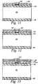
- FIG. 7illustrates the sample after coating of the substrate with the passivation layers.
- FIG. 8illustrates the sample in a single pixel region after deposition of the gate material.
- FIG. 9is a detailed view of a portion of a first mask used to fabricate the gate electrodes of the thin film transistor array backplane of the present invention.
- FIGS. 10 a and 10 billustrate the sample in a single pixel region after patterning of the gate electrode and line.
- FIG. 11is a cross sectional view of the sample in a single pixel area after deposition of the gate insulating layer
- FIG. 12is a cross sectional view of the sample in a single pixel area after deposition of the channel layer.
- FIG. 13is a cross sectional view of the sample in a single pixel area after deposition of the contact layer.
- FIG. 14is a cross sectional view of the sample in a single pixel area after deposition of the source-drain layer.
- FIGS. 15 a and 15 billustrate the sample after patterning the source and drain electrodes.
- FIG. 16is a detailed view of a portion of a second mask used to pattern the source and drain electrodes, lines and pads in the thin film transistor array backplane of the present invention.
- FIG. 17is a detailed view of a portion of a third mask used to pattern the transistor islands in the thin film transistor array backplane of the present invention
- FIGS. 18 a and 18 billustrate the sample after patterning of the transistor islands.
- FIG. 19is across sectional view of the sample in a single pixel area after deposition of the protective layer.
- FIG. 20is a detailed view of a portion of a fourth mask used in a final lithography step to fabricate the thin film transistor array backplane of the present invention.
- FIG. 21is a detailed overlay of the first, second, third and fourth masks.
- FIG. 22is a SEM showing the source-drain electrodes of a backplane of an illustrative embodiment of the present invention.
- FIG. 23is a graph of a source-drain current as a function of a gate voltage in a thin film transistor array backplane of the present invention.
- FIG. 24is a graph of a source-drain current as a function of a source-drain voltage in a thin film transistor array backplane of the present invention.
- FIG. 25is a schematic cross section of a pixel area of a flexible display including a thin film transistor array backplane of the present invention.
- FIG. 26illustrate a shopping cart implementing the flexible backplane of the present invention.
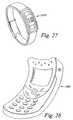
- FIG. 27illustrates a wristwatch implementing the flexible backplane of the present invention.
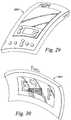
- FIG. 28illustrates a cell phone implementing the flexible backplane of the present invention.
- FIG. 29illustrates a PDA implementing the flexible backplane of the present invention.
- FIG. 30illustrates a fuel gauge implementing the flexible backplane of the present invention.
- the present inventionprovides an improved active matrix backplane comprising an array of amorphous silicon thin-film transistors fabricated on a polyimide substrate.
- the thin-film transistor componentsare deposited on the polyimide substrate by plasma enhanced chemical vapor deposition.
- the present inventionwill be described below relative to an illustrative embodiment. Those skilled in the art will appreciate that the present invention may be implemented in a number of different applications and embodiments and is not specifically limited in its application to the particular embodiments depicted herein.
- FIG. 1is a broad illustration of an electronic label suitable for implementing the thin-film transistor active matrix backplane of an illustrative embodiment of the invention.
- the electronic labelmay be employed in connection with an item, person, animal or location in accordance with the teachings of the present invention.
- the illustrated electronic label 16is specifically employed in connection with an item 12 .
- the electronic label 16displays information, generally as human or machine readable indicia 14 , in order to display information related to the item 12 or any other predefined or selected information.
- the electronic label 16can be temporarily or permanently affixed, attached, secured or coupled to the item 12 according to known methods and techniques.
- a suitable conventional mechanical fastening systemsuch as fasteners, loop and hook-type arrangements, stitches, adhesives, and molding, as well as other known fixation techniques, can be employed to permanently or temporarily attach the electronic label 16 to the item 12 .
- the labelcan also be integrally formed with the item, or can be used as a stand alone label.
- the term labelis intended to include a label, strip, tag or general display device that is sufficiently sized and configured for attachment to an animal, person, item, or location for displaying indicia.
- the label 16is generally shown and described as being attached to an item, although those of ordinary skill will readily recognize that the label can also be attached to an animal, person or location.
- the labelmay also be a stand alone display that is not mounted to anything, such as business cards or trading cards.
- the labelmay comprise electronic paper writing for drawing, printing, copying or faxing.
- the illustrated electronic label 16displays information that is either wholly or partly prestored or preloaded, or uploaded, in the label, or created by a processor in the label, or displays information that corresponds or is consistent with or based upon signals received from an-external source, such as an activator module and/or a GPS system.
- an-external sourcesuch as an activator module and/or a GPS system.
- the information displayed by the electronic label 16can be any general information corresponding to the item, location, mammal or non-mammal, and which is suitable and appropriate for a particular intended use.
- the electronic label 16comprises a transistor backplane 20 built on a substrate 21 and a functional front plane 22 comprising a display medium forming a pixel addressable display.
- Each pixel of the display assemblycan be individually altered by a thin-film transistor in the array of thin-film transistors in the activation grid matrix.
- a thin-film transistoris formed on each pixel region for addressing the corresponding pixel in the display.
- Each thin-film transistorcontrols or measures the voltage imposed on each pixel.
- Each transistoris in turn controlled by a matrix of gate lines and data lines.
- the transistor backplaneis first built on a substrate.
- the functional front plane (display material) 22is added on top of the transistor backplane and a top electrode 24 , comprising, for example ITO (indium tin oxide) or similar transparent conducting material on a substrate is deposited over the display layer 22 .
- a top electrode 24comprising, for example ITO (indium tin oxide) or similar transparent conducting material on a substrate is deposited over the display layer 22 .
- the top electrode 24can be a hand held or mechanically moved wand or stylus.
- the transistor backplane 20comprises an array of silicon-based thin film transistors to form an active matrix for controlling the display. Each pixel can be selectively activated to form a desired symbol, indicia, number, bar code and so on.
- the display medium used in the front plane 22may comprise any suitable electronically activated (current or voltage) flexible display or imaging material known in the art.
- the display mediumcan be bi-stable, non-volatile or stable only when power is applied or very slow to change after power is removed.
- the display mediummay be used to form black and white or color images and may comprise a single or multiple transistors per pixel.
- the display medium in the front planecan be any material that changes state in response to a current or voltage, including, but not limited to LCD, OLED, phosphorus, electrophoretic ink, flexible cholesteric, rigid cholesteric, GyriconTM, micro-encapsulated Gyricon balls, E InkTM material, a polymer dispersed liquid crystal (PDLC) film, and non volatile liquid crystals such as; Cholesteric, Fast Multi Stable Liquid Crystals (FMLCD), Bi-stable nematic liquid crystal, Zenithal, as well as ferroelectric, OnyxTM materials and so on. Suitable materials are described in U.S. patent application Ser. No. 09/393,553, filed Sep. 10, 1999, U.S. patent application Ser. No. 09/760,363, filed Jan. 12, 2001 and U.S. patent application Ser. No. 10/071,732 filed Feb. 7, 2002, the contents of all of which are herein incorporated by reference.
- the pixels in the displaymay have any size, area and shape, including, but not limited to square, round, hexagonal or any other type of polygon.
- the number of pixels and overall size and shape of the addressable matrixcan be increased according to the particular application.
- FIG. 2 cillustrates an electronic label 16 ′ including an RFID layer according to anther embodiment of the invention.
- the label 16 ′includes an RFID layer 28 , a layer comprising an active matrix grid 20 , a layer 22 comprising a display medium, a layer 24 comprising a reference electrode, and a top protection layer 25 .
- the row and column lines in the backplane layerconnect to pads on integrated circuits in the RFID layer 28 .
- the driver and addressing circuitscan be located in the integrated circuit chips, created by using discrete components or fabricated during the backplane manufacturing process directly on to the backplane substrate material.
- FIG. 3is a top view of the transistor backplane 20 of an illustrative embodiment of the invention.
- the transistor back plane 20includes a matrix of gate lines 27 and data lines 26 for controlling each thin-film transistor in the array, thereby forming the pixel addressable, active matrix.
- the gate lines and data lines that form the addressable, active matrix backplane 21can be connected with drive circuitry (not shown) using routing and connecting methods known in the art.
- FIG. 4illustrates an overhead view of a portion of the backplane 20 , illustrating the pixel structure of the backplane 20 according to an illustrative embodiment of the invention.
- the backplane 20comprises an array of pixels formed by thin-film transistors 30 , four of which are completely shown in FIG. 4.
- FIG. 5illustrates a schematic cross-sectional view through a single integrated transistor 30 of the pixel array forming the active matrix thin-film transistor array backplane 20 .
- FIG. 6is an overhead view of the backplane layout in a single pixel region.
- the transistorcomprises a plurality of layers stacked on top of each other and patterned to define the thin-film transistor structure.
- the thin-film transistorshave a bottom gate, back-channel etch structure.
- each transistorincludes a flexible polyimide substrate 32 having a first passivation layer 34 on a top surface and a second passivation layer 36 on the bottom surface of the substrate 32 .
- the polyimide substrateis Kapton E film, manufactured by DuPont, and the passivation layers 34 , 36 comprise SiN x .
- the transistor 30further includes a patterned layer of gate material 40 forming a gate electrode and line.
- the gate material 40comprises a bilayer of aluminum (Al) and Chromium (Cr) deposited on the surface of the first passivation layer 34 .
- a gate insulating layer 44is deposited over the patterned gate electrode layer 40 and top passivation layer 34 .
- the insulating layer 44comprises SiN x , as well.
- the transistor 30further includes one or more semiconducting channel layers 50 deposited over the gate insulating layer 44 .
- the illustrative semiconducting channel layer 50comprises amorphous silicon (a-Si:H) deposited over the insulating layer 44 .
- a contact layer 52illustrated as a layer of phosphorus doped amorphous silicon ((n+)a-Si:H), is deposited on the channel layer 50 .
- a source-drain layer 60is deposited over the contact layer and patterned to define source and drain electrodes, lines ( 82 in FIG. 6) and pads ( 84 in FIG. 6) for the thin-film transistor.
- the contact layer 52is disposed between the source and drain lines 60 of the thin-film transistor. The layers are etched to define the thin-film transistor structures.
- the top layer 70 of the transistorcomprises a protective layer for protecting the components of the transistor and providing electrical insulation to the source lines and transistor islands.
- the layersare etched to define a thin-film transistor island 57 in the channel layer 50 , the pixel areas, gate buslines 25 and data buslines 26 .
- the protective top layer 70is etched to remove unwanted material over the drain pads 84 of the thin-film transistor 30 to expose the active pixel areas.
- the thin-film transistor arrayis fabricated by sequentially depositing and patterning the various layers on the prepared polyimide substrate 32 .
- the handling of the polyimide substrate 32 during fabrication of the thin-film transistor arrayis done as free standing film.
- the polyimide substrate 32is not glued to a solid support followed by processing, but rather, attached by clips at the corners or held at the edges using any suitable fastening technique during certain processes, such as photolithography and deposition.
- the sample, including the polyimide substrate 32may be held in place using an aluminum plate having an array of small holes connected to the vacuum source of the spin coater. The force generated by the vacuum holds the sample in place on the aluminum plate during spinning.
- the polyimide substrate 32is first cleaned prior to deposition of the various layers.
- the polyimide substrate 32may be initially cleaned with deionized water in an ultrasonic bath, such as the Branson 3510 Ultrasonic Bath.
- the polyimide substrate 32may then be placed in a plasma enhanced chemical vapor deposition (PECVD) chamber, such as a multi-chamber S900 PECVD manufactured by System innovative Systems Engineering, to clean the deposition surface of the polyimide substrate 32 .
- PECVDplasma enhanced chemical vapor deposition
- the deposition surfacemay be cleaned by exposing the substrate to an argon plasma.
- the surfaceis exposed to the argon plasma for about two minutes at a pressure of between about 0.1 and about 1.0 Torr and preferably 0.5 Torr and an rf power density of about 0.01 to about 0.05 and preferably 0.022 watts per centimeter squared at between about 100° Celsius and about 250° Celsius and preferably at about 150° Celsius.
- a suitable plasma generator and system for the cleaning stepis the ENI ACG-3B RF Plasma Generator and Advanced Energy Industries AM5 Matching Network, though one skilled in the art will recognize that any suitable system and method for cleaning the deposition surface of the polyimide substrate may be used.
- the polyimide substrate 32is a flexible film having a thickness of between about 25 microns and about 100 microns, and preferably between about 45 and about 55 microns and most preferably about 51 microns, though one skilled in the art will recognize that the invention is not limited to the described thickness.
- the substrate 32may comprise plastic, PET, PEN, polyester, high temperature polymers or other suitable flexible material.
- the passivation layers 34 , 36are deposited on the polyimide substrate 32 to provide isolation and passivation of the polyimide substrate. Passivation of the substrate provides a standardized substrate surface that is a barrier to moisture and solvent uptake by the polyimide substrate and provides adhesion to the subsequent thin-film transistor layers. Prior to deposition of the passivation layers, the deposition chamber is flushed.
- the first passivation layer 34comprising SiN x , is deposited on the top deposition surface, which will contain the thin-film transistors, using a mixture of H 2 , SiH 4 and NH 3 at between about 100° Celsius and about 250° Celsius and preferably about 150° Celsius at a pressure between 0.2 to 0.8 Torr, preferably 0.5 Torr, and a rf power density between 0.07 to 0.3, preferably 0.067, watts per centimeter squared.
- the gases and flow rates for depositing the passivation layerare SiH 4 at about between 2 to 10 standard cubic centimeters/minute and preferably about 5 standard cubic centimeters/minute, H 2 at between about 100 to about 400 standard cubic centimeters/minute and preferably about 220 standard cubic centimeters/minute, and NH 3 at about between 20 to 80 standard cubic centimeters/minute and preferably about 50 standard cubic centimeters/minute.
- the second passivation layer 36also comprising SiN x , is deposited on the bottom side of the polyimide substrate 32 in a similar process to isolate and passivate the substrate.
- FIG. 7is a cross-sectional view of a single pixel of the backplane sample 20 at this stage of the fabrication process.
- the passivation layers 34 , 36have a thickness of between about 250 nanometers and about 1000 nanometers, and preferably about 500 nanometers.
- the passivation layersmay have any suitable thickness.
- the gate electrodes 42 , lines 43 and padsare fabricated on the coated substrate using e-beam evaporation and photolithography.
- the gate material forming the gate electrode layer 40comprises a first gate material, preferably aluminum, deposited on the passivation layer and an overcoat gate material, preferably chromium, deposited over the first gate material.
- the first gate materialhas a thickness of between about 500 and about 5000 Angstroms and preferably about 1000 Angstroms.
- the second gate materialpreferably has a thickness of between about 50 and about 200 Angstroms and more preferably about 100 Angstroms.
- the first gate material and overcoat gate materialare deposited on the top surface of the first passivation layer 34 under high vacuum using an e-beam evaporator, such as the Ebeam Evaporator from Denton Vacuum, to form a thin film 40 of the gate material over the first passivation layer 34 .
- an e-beam evaporatorsuch as the Ebeam Evaporator from Denton Vacuum
- Other techniques for thin-film metallizationcan be used in accordance with the present invention.
- FIG. 8is a cross-sectional view of the sample after deposition of the gate material.
- the gate material 40has a thickness of between about 50 nanometers and about 500 nanometers, and preferably about 100 namometers.
- the inventionis not limited to the described range and that the layer of gate material may have any suitable thickness.
- the gate electrodes 42 , lines 43 and padsare patterned with a gate mask 400 , illustrated in FIG. 9, using photolithography.
- the gate mask 400 shown in FIG. 9illustrates the first 5 ⁇ 6 pixels in the array.
- the maskincludes alignment marks 402 to assist in precisely aligning the mask 400 on the substrate and features 404 and 406 defining the gate electrodes and lines, respectively.
- the mask 400is aligned with the coated substrate, so that the pattern on the mask can be transferred onto the surface of the first passivation layer 34 .
- the top surfaceis first spin coated with an adhesive promoter, such as hexamethyldisilane (HMDS), followed by application of a photoresist, such as AZ5214 2 photoresist commercially available from Clariant Corporation of Somerville, N.J., and spin coating to produce a thin uniform layer of photoresist.
- an adhesive promotersuch as hexamethyldisilane (HMDS)
- a photoresistsuch as AZ5214 2 photoresist commercially available from Clariant Corporation of Somerville, N.J.
- spin coatingto produce a thin uniform layer of photoresist.
- the sampleis spin coated at about 4000 revolutions per minute for about forty seconds, though other suitable rates and times may be used.
- the sampleis soft-baked in an oven to remove substantially all of the solvents from the photoresist coating.
- the sampleis soft-baked in an oven at about 90° Celsius for about twenty minutes, though other temperatures and times may be used.
- the exposure time for developing the electrodesmay be about 50 to about 100 seconds and preferably 71.5 seconds at about 0.5 to about 3.0 milliwatts per centimeter, preferably 2.0 milliwatts per centimeter squared at a pressure of about 2 mBar pressure using a 1:1 AZ312 developer.
- the chromium overcoat layeris then etched for about 40 seconds by treating the chromium with a Ce +4 based etchant solution, such as the CR-7 Chromium Photomask Etchant solution from Cyantek Corporation, following by washing the sample with deionized water and hard-baking the sample.
- the sampleis hard baked at about 115° C. for about twenty minutes.
- the remaining unwanted aluminum in the first gate layeris removed using a suitable solution, such as, but not limited to, a solution comprising a mixture of 85% phosphoric acid, 5% deionized water, 5% acetic acid and 5% nitric acid.
- a suitable solutionsuch as, but not limited to, a solution comprising a mixture of 85% phosphoric acid, 5% deionized water, 5% acetic acid and 5% nitric acid.
- the photoresist layermay be removed using acetone in an ultrasonic cleaning bath or through other suitable means known in the art.
- FIG. 10Ais a cross-sectional view of the sample and FIG. 10B is a top view of the backplane sample 20 in a single pixel area after patterning of the gate electrodes 42 and lines 43 using the first mask 400 .
- the first gate layer of the gate electrode 40comprises titanium, rather than aluminum.
- titaniumrather than aluminum.
- other metalsmay be used to form the gate electrodes and that the invention is not limited to aluminum or titanium.
- the patterned substrateis placed in the PECVD deposition chamber to deposit the gate insulation layer 44 over the patterned gate layer 40 using plasma enhanced chemical vapor deposition.
- the gate insulation layer 44may be deposited in a manner similar to the process for depositing the passivation layers 34 , 36 , as described above, using a gas mixture of hydrogen, SiH 4 , and NH 3 .
- the gate insulation layeris deposited at a temperature of between about 100° Celsius and about 250° Celsius and preferably about 150° Celsius, a pressure of between about 0.1 and about 1.0 Torr and preferably 0.5 Torr, and an rf power density of between about 0.01 and about 1.0 and preferably about 0.067 watts per centimeter squared.
- the argon plasma treatment stepis 2 minutes at between 0.07 to 0.3, and preferably 0.022, watts per centimeter squared.
- the gases and flow rates for depositing the insulation layerare SiH 4 at about between 2to 10 standard cubic centimeters/minute and preferably about 5 standard cubic centimeters/minute, H 2 at about between 100 to 400 standard cubic centimeters/minute and preferably about 220 standard cubic centimeters/minute, and NH 3 at about between 20 to 80 standard cubic centimeters/minute and preferably about 50 standard cubic centimeters/minute.
- FIG. 11is a cross sectional view of the sample 20 in a single pixel area after deposition of the gate insulating layer 44 .
- the gate insulating layer 44is between about 150 and about 700 nanometers thick and preferably about 360 nanometers thick.
- the inventionis not limited to the described range and that the gate insulating layer may have any suitable thickness.
- the samplemay then be transferred to another chamber to deposit the channel layer or layers 50 .
- a mixture of SiH 4 and H 2are used to deposit a layer of amorphous silicon (a-Si:H) over the gate insulating layer 44 .
- the layeris about 2000 angstroms thick, though the invention is not limited to the described thickness.
- the amorphous silicon layeris deposited at a pressure of between about 0.1 to about 1.0 Torr and preferably 0.5 Torr, an rf power density of between about 0.01 and about 1.0 and preferably about 0.027 watts per centimeter squared and a temperature of between about 100° Celsius and about 250° Celsius and preferably about 150° Celsius for about 1900 seconds in the illustrative embodiment, though other parameters may be used.
- the gases and flow rates for depositing the channel layerare SiH 4 at between about 10 to about 40 standard cubic centimeters/minute and preferably about 20 standard cubic centimeters/minute and H 2 at between about 10 to about 40 standard cubic centimeters/minute and preferably about 20 standard cubic centimeters/minute.
- the channel layer 50may comprise p-Si:H or other suitable material.
- FIG. 12is a cross sectional view of a single pixel of the sample 20 after deposition of the channel layer 50 .
- the channel layer 50is between about 100 and about 400 nanometers thick and preferably about 200 nanometers thick.
- the inventionis not limited to the described range and that the channel layer may have any suitable thickness.
- the sampleis transferred to another chamber to deposit the contact layer 52 .
- the chamberis first pumped out and the contact layer, comprising phosphorus doped amorphous silicon, is deposited at a pressure of about 0.1 to 1.0 Torr and preferably 0.5 Torr for about 400 seconds using a rf power density of between about 0.07 and about 0.3, and preferably 0.018, watts per centimeter squared.
- FIG. 13is a cross-sectional view of the sample after deposition of the contact layer 52 .
- the contact layermay have a thickness of between about 25 nanometers and about 100 nanometers.
- the contact layer 52is a film of about 50 nanometers thickness.
- the gases and flow rates for depositing the contact layerare SiH 4 at about 44 sscm and about PH 3 at about 6 sscm.
- FIG. 14is a cross-sectional view of the sample after deposition of the source-drain metal.
- the source-drain layerhas a thickness of between about 50 nanometers and about 200 nanometers and preferably about 100 nanometers.
- the material forming the source-drain layer 60comprises a bi-layer of aluminum and chromium.
- the source-drain layer 60may comprise a tri-layer comprising a first layer of chromium, an intermediate layer of aluminum and a top layer of chromium.
- FIGS. 15 a and 15 billustrate the sample after patterning the source-drain electrodes.
- a portion of a source and drain electrode mask 600 for patterning the array of source and drain electrodes, lines and padsis illustrated in FIG. 16.
- the mask 600includes alignment marks 601 for aligning the mask on the substrate.
- the maskalso includes source electrode patterns 603 , drain electrode patterns 602 , line patterns 604 and pad patterns for each pixel in the array.
- the top surfaceis first spin coated with an adhesive promoter, such as HMDS, followed by photoresist spin coating at 4000 rpm for 40 seconds, preferably using AZ5214 photoresist. Then, the sample is soft-baked in an oven, for example, at about 90° C. for about twenty minutes, followed by patterning of the source-drain structure.
- the source-drain structuremay be patterned using a contact aligner, such as the Karl Suss MA6 Aligner.
- a suitable exposure timeis about 50 to 100 seconds, preferably 71.5 seconds and a suitable light fluence is about 0.5 to 3.0 milliwatts per centimeter, preferably 2.0 milliwatts per centimeter.
- the source-drain electrodes 62 , 63may be developed for about sixty seconds in a 1:1 AZ312 developer, rinsed in deionized water and then baked at about 115° C. for about twenty minutes.
- the unwanted source-drain materiali.e., the aluminum and/or chromium
- the unwanted aluminum materialis removed with a mixture of about 85% phosphoric acid, 5% deionized water, 5% acetic acid and 5% nitric acid.
- the samplemay then be washed, for example, using deionized water, and subsequently hard-baked at 115° C. for about twenty minutes.
- the phosphorus-doped layermay be etched using a plasma etcher, such as the Plasma-Therm 790 System. Suitable etching conditions are about 150 mbar, 16 standard cubic centimeters per minute (sccm) of CF 4 and 0.12 watts per centimeter squared for a total of about seven minutes, though other suitable parameters may also be used.
- the second mask photoresist layermaybe removed using any suitable means, such as acetone in an ultrasonic cleaning bath.
- an array of transistor islands 57are patterned using photolithography.
- a portion of the transistor island mask 900is shown in FIG. 17.
- the transistor island mask 900includes alignment marks 901 and an array of transistor island features 870 .
- the top surfaceis first spin coated with an adhesive promoter, such as HMDS, followed by AZ5214 photoresist and spin coating.
- an adhesive promotersuch as HMDS
- AZ5214 photoresist and spin coatingIn one example, the sample is spin coated at about 4000 rpm for about 40 seconds. The sample may then be soft-baked in an oven to remove substantially all of the solvents from the photoresist coating.
- the exposure timeis about 50 to 100 seconds, preferably 71.5 seconds and the light fluence is about 0.5 to 3.0 milliwatts per centimeter, preferably 2.0 milliwatts per centimeter.
- the array of transistor islands 57may be developed for about sixty seconds using a developer, such as 1:1 AZ312 developer in deionized water. After development of the transistor islands 57 , the sample is rinsed in deionezed water and baked in an oven at about 115° C. for about twenty minutes. Then, the amorphous silicon channel layer 50 may be etched using a plasma etcher, such as the Plasma-Therm 790 System VII. Suitable etching conditions are known in the art.
- the etching conditionsare 150 mbar, 16 standard cubic centimeters/minute CF 4 and 0.12 watts per centimeter squared until the amorphous silicon layer is removed.
- the etching conditionsare not limited to the described range.
- the remaining transistor island mask photoresist layermay be removed through suitable means, such as by using acetone in an ultrasonic cleaning bath.
- FIGS. 18 a and 18 bare cross-sectional and overhead views, respectively, of the sample 20 after patterning of the transistor islands 57 out of the channel layer material 50 as described above.
- the protective layer 70is deposited to complete the thin film transistor backplane.
- FIG. 19is a cross-sectional view of the sample after deposition of the protective layer 70 .
- the protective layercomprises a layer of SiN x that is between about 130 and about 500 nanometers thick, and preferably about 260 nanometers thick, though one skilled in the art will recognize that the invention is not limited to the described thickness.
- the protective layer 70may be deposited using plasma enhanced chemical vapor deposition, as described above, using a mixture of H 2 , SiH 4 and NH 3 at a temperature of between about 100° Celsius and about 250° Celsius and preferably about 150° Celsius and a pressure of about 0.1 to 1.0 Torr and preferably 0.5 Torr at between about 0.01 and about 1.0 and preferably about 0.067 watts per centimeter squared.
- the gases and flow rates for depositing the protective layerare SiH 4 at about between 2 to 10 standard cubic centimeters/minute and preferably about 5 standard cubic centimeters/minute, H 2 at about between 100 to 400 standard cubic centimeters/minute and preferably about 220 standard cubic centimeters/minute, and NH 3 at about between 20 to 80 standard cubic centimeters/minute and preferably about 50 standard cubic centimeters/minute.
- the protective layeris etched to remove unwanted material over the drain pads 84 of the thin-film transistor 30 to expose the active pixel areas, thus forming the final structure shown in FIG. 5.
- the top surfaceis spin coated with an adhesive promoter, such as HMDS, followed by application of a photoresist layer, such as AZ5214 and spin coating at about 4000 revolutions per minute for about forty seconds.
- the samplemay then be soft-baked in an oven at about 90° C. for about twenty minutes.
- a final lithography stepmay be patterned using a contact aligner, such as the Karl Suss MA6 Aligner using a fourth mask 700 , shown in FIG.
- the mask 700includes alignment marks 701 and an array of drain pad features 701 .
- the gate insulator layer 44 and the top protective layer 70are removed to expose the drain electrodes, gate pads and source pads using reactive ion etching (RIE).
- RIEreactive ion etching
- the drain electrodes, gate pads and source padsare exposed using a Plasma-Therm 790 System VII at 100 mbar, 35 standard cubic centimeters/minute of CF 4 , 5 standard cubic centimeters/minute of O 2 and 0.16 watts per centimeter squared for about 8 minutes.
- the remaining photoresist of the fourth mask 700may be removed using acetone in an ultrasonic cleaning bath or other suitable means.
- FIG. 22illustrates a SEM of source and drain electrodes in a backplane fabricated according to an illustrative embodiment of the invention.
- the transistor backplane 20may be annealed in a forming gas, such as a mixture of H 2 in N 2 gas, at elevated temperatures.
- a suitable mixtureis 15% H 2 in N 2 for about 1 hour at about 195° C.
- the electrical characteristics of the transistor backplane 30may be measured using a semiconductor analyzer during fabrication.
- FIGS. 23 and 24illustrate the typical characteristics of the sample after patterning of the transistor islands.
- FIG. 22illustrates a source-drain current as a function of a gate voltage in the thin film transistor array backplane 30 of the present invention, measured with drain voltages of 0.1 and 10 volts.
- the deviceis suitable for high-resolution displays with an ON/OFF ration of about 10 6 when the gate voltage varies between 0 and 20 volts.
- FIG. 23is a graph of a source-drain current as a function of a source-drain voltage in a thin film transistor array backplane of the present invention.
- the fabricated array 20 of thin-film transistors 30may be used as a flexible display by laminating, attaching or mounting a display medium to the backplane 20 .
- a polymer dispersed liquid crystal (PDLC) display 100may be fabricated by curing a 20:80 mixture 104 of prepolymer PN393 and TL213, both available from EM Industries) between the active matrix thin-film transistor array 20 and a sheet of ITO (indium tin oxide) coated polyester 102 , from ISF Innovative Specialty Films, using a light source of about 3.0 milliwatts per centimeter squared and an exposure time of about twenty minutes. Two glass plates may be used to sandwich the composite during curing. Fiber spacers may be used to control the spacing between the drain pad and the ITO layer 102 .
- PDLCpolymer dispersed liquid crystal
- FIGS. 26-30illustrate applications of the flexible backplane in display assemblies, which are no longer bound by the limitations of flat glass or a flat backplane.
- the displayscan be wrapped or bent in more than one place.
- FIG. 26illustrates an application of the flexible backplane of the invention in a round handle of a shopping cart 310 .
- the flexible backplaneforms a display 311 that can be used to inform shoppers of specials or provide information.
- FIG. 27illustrates a watch 270 where the face of the watch has the same convex shape in multiple dimensions as the band.
- the ability to have a convex displaycreates a smooth, contour shape.
- Other embodimentsinclude ID wristbands, calculators or a display on any type of recording or playback device, radio, television, clock or home appliance with a retractable/roll-up display.
- FIG. 28illustrates a cell phone 280 in which the display or imaging area is contoured so that the entire phone fits better against the listener's ear or in the user's hand or pocket.
- Other embodimentsinclude calculators or a display on any type of recording or playback device, radio, television, clock, home appliance, electronic game set top boxes and so on.
- FIG. 29illustrates a PDA 290 with a convex display that allows any information displayed to be more easily read.
- FIG. 30illustrates a fuel gauge 300 used in a car or truck.
- the flexible backplaneenables the freedom to contour gauges into dashboard or panels in a safer design than flat displays and provides greater freedom in designing the interior of any type of vehicle.
- the flexible backplanemay be implemented in any suitable type of gauge or instrument.
- the display using the active matrix thin-film transistor array backplane of the inventionpossesses a resolution of about 51 dpi, with 3600 pixels on an active display area of about 3 centimeters squared.
- the display using the backplane of the inventionmay also be manufactured in sized of 8.5 by 14 inches or larger, to allow creation of electronic paper for writing, drawing, printing, copying or faxing.
- One skilled in the artwill recognize that the invention is not limited to the described size, shape or dpi and that a backplane have varied parameters is embodied by the present invention.
- the active matrix thin film transistor array backplane of the present invention and the described method of manufacturing the active matrix thin film transistor array backplaneprovide significant advantages over the prior art.
- the backplaneis a compliant, flexible structure that is not damaged when bent, allowing a display formed using the backplane to be conformable to a variety of surfaces and items.
- the flexible substratemakes possible efficient manufacturing methods, such as roll to roll processing and photoresist-free fabrication techniques that can lower overall manufacturing costs.
- the backplaneis lightweight and stronger than prior thin-film transistors formed on glass substrates.
- the backplaneprovides high-resolution displays that are easily controlled and updated.
- the backplane and displays using the backplanes of the inventionare rugged, conformable, robust resistant to failure, lightweight and non-breakable.
- the backplaneis resistant to strain and performs substantially the same under compressive strain and when lying flat.
- the deviceis also stable to elevated temperature and humidity.
- the backplane fabricated on polyimide according to the present inventionperforms substantially identically to backplanes formed on glass substrates, while reducing cost, and providing a more lightweight and robust product.
- Flexible active matrix matrix TFT array backplaneswere fabricated on 51 ⁇ m thick polyimide foil (Kapton® E) substrates, as described in the article by C. E. Forbes, A. Gelbman, C. Turner, H. Gleskova, and S. Wagner entitled “A Rugged Conformable Backplane Fabricated with an a-Si:H Array on a Polyimide Substrate,” SID '02 Digest, 33, 2000 (2002). This article is incorporated herein by reference.
- the substrate used for the flexible backplanewas a three inch square of 51 ⁇ m thick Kapton® foil, which is available from DuPont Films.
- Kapton® foilwhich is available from DuPont Films.
- Corning 1727 glasswas used as the substrate for the rigid non-flexible backplane.
- both sides of the substratewere coated with 500 nm thick SiNx layers.
- the filmwas processed as a free-standing substrate.
- the glass substratewas coated with SiNx (500 nm) on the device side only using the same recipe.
- PECVDwhich the gasses SiH4, H2 and NH3 at 150° C., was used for the deposition. Recipes were optimized to minimize stresses in the substrate with the goal of achieving a flat and stress-balanced film after both SiNx depositions were complete. After the SiNx passivation steps, the glass and Kapton backplanes were processed identically.
- the TFTshave a bottom gate, back-channel etch structure.
- the gate structurewas first fabricated by electron beam metal evaporation (110 nm). Photolithography and wet etching were then used to pattern the gate lines. PECVD (three chambers) was used for the second 360 nm layer of SiNx, followed by a 200 nm a-Si:H layer from SiH4, H2 and PH3. Deposition temperatures were 150° C. and recipes were optimized for Kapton substrates.
- the source and drain electrodeswere made using photolithography with a 120 nm metallization layer. The channel length was 20 ⁇ n and width was 120 ⁇ m. Reactive ion etching (RIE) with photolithography was used to pattern the transistor islands.
- the final SiNx layer(230 nm) was patterned using photolithography and RIE to expose the active pixel areas.
- the TFT Kapton substrateswere bent against a radius of curvature for a set time, followed by measurements of the TFT electrical properties. TFT characteristics were measured after the back (bottom) SiNx protective layer was removed in order to provide a compliant substrate. After this procedure, the radius of curvature of the backplane sample decreased from 18 cm to 9 cm.
- a test jigconstructed from 2-inch ID PVC pipe, was used to stress the sample for 20 minutes and allow measurement of the TFT characteristics while the sample was under inward compressive bending at a radius of 2.5 cm. The in situ measurement gave experimentally similar results to the unstressed sample. More severe bending experiments down to an inward radius of curvature of 1.6 cm, followed by random testing of the TFTs, indicated no catastrophic failure of the TFTs.
- a 3 in. ⁇ 3 in. piece of Kapton Polyimide from DuPontwas carefully cleaned with DI water in a Branson 3510 Ultrasonic Bath prior to being placed in a multi-chamber S900 PECVD manufactured by System innovative Systems Engineering. Under high vacuum, the sample was exposed to argon plasma (ENI ACG-3B RF Plasma Generator and Advanced Energy Industries AM5 Matching Network) for 2 minutes at a pressure of 0.5 Torr and 0.22 W/cm at 200° C. in order to clean the deposition surface. After flushing the deposition chamber, a passivation SiNx layer (3600 angstroms) was deposited on the top surface using a mixture of H2, SiH4 and NH3 at 200° C. at 0.5 Torr and 0.067 W/cm 2 . This process was repeated on the bottom side of the polyimide substrate.
- argon plasmaENI ACG-3B RF Plasma Generator and Advanced Energy Industries AM5 Matching Network
- the gate electrodes, lines and padswere made from a deposited bilayer of aluminum (1000 angstroms) and an overcoat of chromium (100 angstroms). These metals were deposited on the top surface of SiNx using a Denton E-beam Evaporator under high vacuum. After metal deposition, photolithography was used to pattern these structures. The top surface was first spin coated with HMDS, followed by AZ5214 photoresist and spin coating at 4000 rpm for 40 seconds. The sample was then soft-baked at 90° C. for 20 minutes.
- the chromium layerwas etched by treating with a Ce +4 based CR-7 Chromium Photomask Etchant solution (Cyanteck Corp), washed with DI water, followed by a hard bake at 115° C. for 20 minutes. The remaining unwanted aluminum surface was removed with a mixture of 85 phosphoric acid:5 m DI water: 5 ml acetic acid: 5 ml nitric acid. The photoresist layer was removed using acetone in an ultrasonic cleaning bath.
- the coated substrate with patterned gate electrodeswas then placed in the multi-chamber PECVD vacuum chamber and deposited with a SiNx 3600angstrom layer with a gas mixture of H2, SiH 4 and NH3 at 200° C. at 0.5 Torr and 0.067 W/cm 2 after a 2 minutes 0.022 W/cm 2 Ar plasma cleaning step. Without breaking the vacuum, the sample was transferred to another chamber used solely for the a-Si:H depositions. A 50:50 mixture of SiH 4 and H2 at 0.5 Torr at 0.027 W/cm 2 at 200° C. for 1900 seconds was used to deposit a 2000 angstrom a-Si:H layer over the SiNx layer.
- the sampledwas then moved to a chamber reserved for (n+)a-Si:H depositions, the reactor chamber was pumped out and the (n+)a-Si:H layer was deposited at a pressure of 0.5 Torr for 400 seconds using 0.018 W/cm 2 , resulting in a film approximately 500 angstroms thick.
- the gasses and flow rateswere SiH 4 (44 sscm) and PH3 (6 sscm).
- the source and drain electrodes, lines and padswere made from a deposited tri-layer of chromium-aluminum-chromium deposited over the top surface of (n+)a-Si:H using the Denton E-beam Evaporator under high vacuum.
- the first chromium layerwas 100 angstroms
- the aluminum layerwas 1000 angstroms
- the second chromium layerwas 100 angstroms.
- photolithographywas used to pattern these structures using a mask.
- the top surfacewas first spin coated with HMDS followed by AZ5214 spin coating at 4000 rpm for 40 seconds. The sample was then soft-baked at 90° C. for 20 minutes.
- the source-drainwas patterned using a Karl Suss MA6 Aligner. The exposure time was 71.5 seconds and the light fluence was 2.0 mW/cm.
- the electrodeswere developed for 60 seconds in 1:1 AZ512 developer:DI water, rinsed in DI water and baked at 115° C. for 20 minutes.
- the unwanted source-drain materialwas removed with a mixture of 85 ml phosphoric acid: Sml DI water: 5 ml acetic acid: 5 ml nitric acid.
- the samplewas washed thoroughly with DI water and hard baked at 115° C. for 20 minutes. Etching conditions were 150 mbar, 16 sccm CF4 and 0.12 w/cm 2 for a total 7 minutes in one minute intervals.
- the mask photoresist layerwas removed using acetone in an ultrasonic cleaning bath.
- the transistor islandswere patterned using the Karl Suss MA6 Aligner using a third mask using photolithography.
- the top surfacewas first spin coated with HMDS, followed by AZ5214 photoresist and spin coating at 4000 rpm for 40 seconds.
- the samplewas then soft-baked at 90° C. for 20 minutes.
- the exposure timewas 71.5 seconds and the light fluence was 2.0 mW/cm.
- the transistor islands patternwas developed for 60 seconds in 1:1 AZ 512 developer: DI water, rinsed in DI water and baked at 115° C. for 20 minutes.
- the a-Si:H layerwas etched using a Plasma-Therm 790 System VII.
- Etching conditionswere 150 mbar, 16 sccm CF4, and 0.i2 w/cm 2 for a total 42 minutes in two minute intervals.
- the remaining photoresist layerwas removed using acetone in an ultrasonic cleaning bath.
- the electrical characteristicswere measured using a HP 4155A Semiconductor Analyzer with the substrates on a probe station inside a metal box to exclude light.
- the samplewas then coated two times with Photoresist AZ5214 on the device side, placed on a hot plate at 105° C. for one minute and then baked for 20 minutes at 90° C. for 20 minutes.
- the samplewas then placed in the Plasmatherm 790 and RIE etched for a total of 16 minutes. Etching conditions were 100 mbar, 35 sccm CF4 and 5 sccm O2 and 0.16 w/cm 2 for a total 16 minutes in two eight minute intervals.
- the samplewas annealed in a mixture of 15% H2 in N2 gas (forming gas) for 66 minutes in an annealing apparatus.
- a thermocouplewas placed outside of the annealing apparatus and the annealing apparatus was placed in a tube furnace. The temperature, while the sample was exposed to a flow of the forming gas at 1 atm, was ramped to 195° C.
Landscapes
- Physics & Mathematics (AREA)
- Chemical & Material Sciences (AREA)
- Nonlinear Science (AREA)
- Dispersion Chemistry (AREA)
- Mathematical Physics (AREA)
- Crystallography & Structural Chemistry (AREA)
- General Physics & Mathematics (AREA)
- Optics & Photonics (AREA)
- Liquid Crystal (AREA)
- Devices For Indicating Variable Information By Combining Individual Elements (AREA)
- Thin Film Transistor (AREA)
Abstract
Description
- This application claims priority to provisional patent application serial No. 60/350,584 entitled “A Flexible Display Utilizing a Thin Film Transistor Array on a Polyimide Substrate” filed Nov. 21, 2001, provisional patent application serial No. 60/333,838 entitled “A Flexible Display or Imaging Area Utilizing a Thin Film Transistor Array on a Polyimide Substrate” filed Nov. 28, 2001, provisional patent application serial No. 60/374,131 filed Apr. 19, 2002 and provisional patent application serial No. 60/382,314 filed May 21, 2002. The present application is related to U.S. Provisional Patent Application Serial No. 60/099,888 entitled “Remotely Updateable and Alterable Electronic Display Based Products And Systems”, filed Sep. 11, 1998, U.S. patent application Ser. No. 09/393,553 entitled “Smart Electronic Label Employing Electronic Ink”, filed Sep. 10, 1999, U.S. patent application Ser. No. 09/760,363 entitled “Smart Electronic Label Employing Electronic Ink”, filed Jan. 12, 2001 and U.S. patent application Ser. No. 10/071,732 filed Feb. 7, 2002 entitled “Smart Electronic Label Employing Electronic Ink”. The aforementioned applications, and the references cited therein, are incorporated herein by reference.[0001]
- The present invention is directed to electronic display devices. More particularly, the present invention is directed to an active matrix thin film transistor array backplane for an electronic display device and a method of fabricating an active matrix thin film transistor array backplane on a polyimide substrate.[0002]
- Recently, there has been considerable interest in the development of thin flexible electronic displays utilizing either steel or plastic based backplanes for driving the display. Currently, many active matrix displays use glass as a substrate material. However, the use of glass has many drawbacks, including that the glass is heavy, inflexible and fragile. With the elimination of fragile glass substrates, it becomes possible to develop new devices for the growing market of lightweight electronic products. Such products include pagers, smart cell phones, radio frequency identification (RFID) tags, and smart cards. Flexible substrates are compatible with efficient manufacturing methods such as roll to roll processing and photoresist-free fabrication techniques that can lower overall manufacturing costs and make the concept of “electronic paper” a reality.[0003]
- Electronic labels comprise a transistor backplane built on a substrate and a functional front plate including a display material forming a display. Because the functional planes are only micrometers thick, the weight of macroelectronic systems is as light as their substrate and encapsulation will allow.[0004]
- The present invention provides a working active matrix thin film transistor array formed on a polyimide substrate. The array forms a backplane for addressing an electronic display. The thin film transistor array incorporates gate electrodes, a gate insulating layer, semiconducting channel layers deposited on top of the gate insulating layer, a source electrode, a drain electrode and a contact layer beneath each of the source and drain electrodes. An insulating encapsulation layer is positioned on the channel layer. The layers are deposited onto the polyimide substrate using plasma enhanced chemical vapor deposition (PECVD) and etched using photolithography to form the backplane.[0005]
- The thin film transistor array may be used to form an electronic display device by laminating, attaching or applying a display medium, such as electronic ink, polymer dispersed liquid-crystal or other display medium, to the thin film transistor array backplane. The display medium is sandwiched between the thin-film transistor array and a top sheet of ITO-coated polyester to form a pixel-addressable display for displaying information. An alternative design utilizes a wand or stylus as the reference electrode, which activates the corresponding pixel or pixels on the thin-film transistor array as it passes over them. The electronic display device using the thin-film transistor array backplane may be used to form black and white or color displays.[0006]
- The resulting form factor is thin, flexible and malleable. It can be fabricated to conform or contour to any shape. Its flexibility allows for devices to be designed that incorporates retractable or roll up displays.[0007]
- The active matrix thin film transistor array on a polyimide substrate described herein can be combined with any other class of electronically activated materials used to form images to create thin flexible displays. Suitable materials include organic light emitting diodes (OLEDs), traditional liquid crystals, and non volatile liquid crystals such as; Cholesteric, Fast Multi Stable Liquid Crystals (FMLCD), Bi-stable nematic liquid crystal, Zenithal, as well as ferroelectric, Onyx™ materials.[0008]
- The thin film transistor array of the present invention may be used in large area electronics, such as electrophoretic information displays which are flexible, lighter in weight and more impact resistant than displays fabricated on traditional glass substrates. The thin film transistor array may be used in creating the display or imaging area for smart, flexible, thin radio frequency driven (RFID) labels; smart, flexible, thin radio frequency driven (RFID) tags or smart electronic labels employing electronic ink, or any non-volatile display medium; or any type of smart or plain card involving a contactless (wireless) connection to an on-board chip employing electronic ink, or any non-volatile display medium.[0009]
- According to one aspect, a method of fabricating a thin film transistor active matrix backplane is provided. The method comprises the steps of providing a polyimide substrate in a plasma enhanced chemical vapor deposition chamber; depositing a first passivation layer to passivate the substrate using plasma enhanced chemical vapor deposition; applying a gate material to the first passivation layer by e-beam evaporation; patterning the gate material using photolithographie techniques to form an array of gate electrodes; depositing a gate insulating layer over the gate electrodes and first passivation layer; depositing a semiconducting channel layer comprising amorphous silicon over the gate insulating layer using plasma enhanced chemical vapor deposition; depositing a contact layer comprising phosphorus doped amorphous silicon on the semiconducting channel layer using plasma enhanced chemical vapor deposition; depositing a source-drain layer on the contact layer; patterning an array of source electrodes, drain electrodes, lines and pads in the source-drain layer using photolithography, patterning an array of transistor islands on the source and drain electrodes using photolithography; depositing a protective layer on the source-drain layer; and exposing the drain electrodes and pads.[0010]
- According to another aspect, a polymer dispersed electronic display is provided. The display comprises a backplane comprising an active matrix thin film transistor array formed on a flexible polyimide substrate; a top layer of indium tin oxide coated polyester; and a middle layer disposed between the backplane and the top plane comprising a 20:80 mixture of prepolymer PN393 and TL213. The middle layer is cured using a light source.[0011]
- According to another aspect of the invention, a method of making a polymer dispersed electronic display is provided. The method comprises the steps of providing an active matrix thin film transistor array backplane formed on a polyimide substrate; depositing a display medium on the active matrix thin film transistor array backplane; depositing a protective layer comprising indium tin oxide coated polyester over the display medium; and curing the display medium between the backplane and the protective layer.[0012]
- According to yet another aspect, a thin film transistor backplane is provided. The backplane comprises a polyimide substrate, a first passivation layer deposited on a deposition surface of the polyimide substrate, an array of gate electrodes and gate lines patterned on the passivation layer, a gate insulating layer deposited over the array of gate electrodes and gate lines; a semiconducting channel layer deposited over the gate insulating layer, a contact layer deposited on and in contact with the channel layer and an array of source electrodes, drain electrodes, lines and pads fabricated on and in contact with the contact layer.[0013]
- The foregoing and other objects, features and advantages of the invention will be apparent from the following description and apparent from the accompanying drawings, in which like reference characters refer to the same parts throughout the different views. The drawings illustrate principles of the invention and, although not to scale, show relative dimensions.[0014]
- FIG. 1 illustrates an electronic label suitable for implementing an illustrative embodiment of the present invention.[0015]
- FIGS. 2[0016]aand2billustrate an electronic label including a backplane of the present invention.
- FIG. 2[0017]cshows an electronic label including an RFID layer and employing the backplane of the present invention according to another embodiment.
- FIG. 3 is a top view of the thin film transistor array backplane of an illustrative embodiment of the invention, showing the pads and general display area.[0018]
- FIG. 4 is an overhead view of the thin film transistor array backplane, showing the pixel structure. In FIG. 4, four complete pixels are shown.[0019]
- FIG. 5 is a schematic cross-section of a single transistor of the thin film transistor array backplane in one pixel region according to an illustrative embodiment of the invention.[0020]
- FIG. 6 is an overhead view of a single pixel region of a thin film transistor array backplane of the present invention.[0021]
- FIG. 7 illustrates the sample after coating of the substrate with the passivation layers.[0022]
- FIG. 8 illustrates the sample in a single pixel region after deposition of the gate material.[0023]
- FIG. 9 is a detailed view of a portion of a first mask used to fabricate the gate electrodes of the thin film transistor array backplane of the present invention.[0024]
- FIGS. 10[0025]aand10billustrate the sample in a single pixel region after patterning of the gate electrode and line.
- FIG. 11 is a cross sectional view of the sample in a single pixel area after deposition of the gate insulating layer[0026]
- FIG. 12 is a cross sectional view of the sample in a single pixel area after deposition of the channel layer.[0027]
- FIG. 13 is a cross sectional view of the sample in a single pixel area after deposition of the contact layer.[0028]
- FIG. 14 is a cross sectional view of the sample in a single pixel area after deposition of the source-drain layer.[0029]
- FIGS. 15[0030]aand15billustrate the sample after patterning the source and drain electrodes.
- FIG. 16 is a detailed view of a portion of a second mask used to pattern the source and drain electrodes, lines and pads in the thin film transistor array backplane of the present invention.[0031]
- FIG. 17 is a detailed view of a portion of a third mask used to pattern the transistor islands in the thin film transistor array backplane of the present invention[0032]
- FIGS. 18[0033]aand18billustrate the sample after patterning of the transistor islands.
- FIG. 19 is across sectional view of the sample in a single pixel area after deposition of the protective layer.[0034]
- FIG. 20 is a detailed view of a portion of a fourth mask used in a final lithography step to fabricate the thin film transistor array backplane of the present invention.[0035]
- FIG. 21 is a detailed overlay of the first, second, third and fourth masks.[0036]
- FIG. 22 is a SEM showing the source-drain electrodes of a backplane of an illustrative embodiment of the present invention.[0037]
- FIG. 23 is a graph of a source-drain current as a function of a gate voltage in a thin film transistor array backplane of the present invention.[0038]
- FIG. 24 is a graph of a source-drain current as a function of a source-drain voltage in a thin film transistor array backplane of the present invention.[0039]
- FIG. 25 is a schematic cross section of a pixel area of a flexible display including a thin film transistor array backplane of the present invention.[0040]
- FIG. 26 illustrate a shopping cart implementing the flexible backplane of the present invention.[0041]
- FIG. 27 illustrates a wristwatch implementing the flexible backplane of the present invention.[0042]
- FIG. 28 illustrates a cell phone implementing the flexible backplane of the present invention.[0043]
- FIG. 29 illustrates a PDA implementing the flexible backplane of the present invention.[0044]
- FIG. 30 illustrates a fuel gauge implementing the flexible backplane of the present invention.[0045]
- The present invention provides an improved active matrix backplane comprising an array of amorphous silicon thin-film transistors fabricated on a polyimide substrate. The thin-film transistor components are deposited on the polyimide substrate by plasma enhanced chemical vapor deposition. The present invention will be described below relative to an illustrative embodiment. Those skilled in the art will appreciate that the present invention may be implemented in a number of different applications and embodiments and is not specifically limited in its application to the particular embodiments depicted herein.[0046]
- FIG. 1 is a broad illustration of an electronic label suitable for implementing the thin-film transistor active matrix backplane of an illustrative embodiment of the invention. The electronic label may be employed in connection with an item, person, animal or location in accordance with the teachings of the present invention. The illustrated[0047]
electronic label 16 is specifically employed in connection with anitem 12. Theelectronic label 16 displays information, generally as human or machinereadable indicia 14, in order to display information related to theitem 12 or any other predefined or selected information. Theelectronic label 16 can be temporarily or permanently affixed, attached, secured or coupled to theitem 12 according to known methods and techniques. According to one practice, a suitable conventional mechanical fastening system, such as fasteners, loop and hook-type arrangements, stitches, adhesives, and molding, as well as other known fixation techniques, can be employed to permanently or temporarily attach theelectronic label 16 to theitem 12. The label can also be integrally formed with the item, or can be used as a stand alone label. As used herein, the term label is intended to include a label, strip, tag or general display device that is sufficiently sized and configured for attachment to an animal, person, item, or location for displaying indicia. For purposes of clarity, thelabel 16 is generally shown and described as being attached to an item, although those of ordinary skill will readily recognize that the label can also be attached to an animal, person or location. The label may also be a stand alone display that is not mounted to anything, such as business cards or trading cards. Alternatively, the label may comprise electronic paper writing for drawing, printing, copying or faxing. - The illustrated[0048]
electronic label 16 displays information that is either wholly or partly prestored or preloaded, or uploaded, in the label, or created by a processor in the label, or displays information that corresponds or is consistent with or based upon signals received from an-external source, such as an activator module and/or a GPS system. Those of ordinary skill will readily recognize that the information displayed by theelectronic label 16 can be any general information corresponding to the item, location, mammal or non-mammal, and which is suitable and appropriate for a particular intended use. - As shown in FIGS. 2[0049]aand2b, the
electronic label 16 comprises atransistor backplane 20 built on asubstrate 21 and afunctional front plane 22 comprising a display medium forming a pixel addressable display. Each pixel of the display assembly can be individually altered by a thin-film transistor in the array of thin-film transistors in the activation grid matrix. A thin-film transistor is formed on each pixel region for addressing the corresponding pixel in the display. Each thin-film transistor controls or measures the voltage imposed on each pixel. Each transistor is in turn controlled by a matrix of gate lines and data lines. To form the electronic label, the transistor backplane is first built on a substrate. The functional front plane (display material)22 is added on top of the transistor backplane and atop electrode 24, comprising, for example ITO (indium tin oxide) or similar transparent conducting material on a substrate is deposited over thedisplay layer 22. This may or may not be covered by a protection layer that encapsulates the structure and protects the components. Alternatively thetop electrode 24 can be a hand held or mechanically moved wand or stylus. According to the illustrative embodiment, thetransistor backplane 20 comprises an array of silicon-based thin film transistors to form an active matrix for controlling the display. Each pixel can be selectively activated to form a desired symbol, indicia, number, bar code and so on. - The display medium used in the[0050]
front plane 22 may comprise any suitable electronically activated (current or voltage) flexible display or imaging material known in the art. The display medium can be bi-stable, non-volatile or stable only when power is applied or very slow to change after power is removed. The display medium may be used to form black and white or color images and may comprise a single or multiple transistors per pixel. According to one embodiment, the display medium in the front plane can be any material that changes state in response to a current or voltage, including, but not limited to LCD, OLED, phosphorus, electrophoretic ink, flexible cholesteric, rigid cholesteric, Gyricon™, micro-encapsulated Gyricon balls, E Ink™ material, a polymer dispersed liquid crystal (PDLC) film, and non volatile liquid crystals such as; Cholesteric, Fast Multi Stable Liquid Crystals (FMLCD), Bi-stable nematic liquid crystal, Zenithal, as well as ferroelectric, Onyx™ materials and so on. Suitable materials are described in U.S. patent application Ser. No. 09/393,553, filed Sep. 10, 1999, U.S. patent application Ser. No. 09/760,363, filed Jan. 12, 2001 and U.S. patent application Ser. No. 10/071,732 filed Feb. 7, 2002, the contents of all of which are herein incorporated by reference. - The pixels in the display may have any size, area and shape, including, but not limited to square, round, hexagonal or any other type of polygon. The number of pixels and overall size and shape of the addressable matrix can be increased according to the particular application.[0051]
- FIG. 2[0052]cillustrates an
electronic label 16′ including an RFID layer according to anther embodiment of the invention. As shown, thelabel 16′ includes anRFID layer 28, a layer comprising anactive matrix grid 20, alayer 22 comprising a display medium, alayer 24 comprising a reference electrode, and atop protection layer 25. - In the[0053]
label 16′ of FIG. 2c, the row and column lines in the backplane layer connect to pads on integrated circuits in theRFID layer 28. The driver and addressing circuits can be located in the integrated circuit chips, created by using discrete components or fabricated during the backplane manufacturing process directly on to the backplane substrate material. - FIG. 3 is a top view of the[0054]
transistor backplane 20 of an illustrative embodiment of the invention. As shown, the transistor backplane 20 includes a matrix ofgate lines 27 anddata lines 26 for controlling each thin-film transistor in the array, thereby forming the pixel addressable, active matrix. The gate lines and data lines that form the addressable,active matrix backplane 21 can be connected with drive circuitry (not shown) using routing and connecting methods known in the art. - FIG. 4 illustrates an overhead view of a portion of the[0055]
backplane 20, illustrating the pixel structure of thebackplane 20 according to an illustrative embodiment of the invention. As shown, thebackplane 20 comprises an array of pixels formed by thin-film transistors 30, four of which are completely shown in FIG. 4. - FIG. 5 illustrates a schematic cross-sectional view through a single[0056]
integrated transistor 30 of the pixel array forming the active matrix thin-filmtransistor array backplane 20. FIG. 6 is an overhead view of the backplane layout in a single pixel region. The transistor comprises a plurality of layers stacked on top of each other and patterned to define the thin-film transistor structure. At each pixel element, the thin-film transistors have a bottom gate, back-channel etch structure. As shown, each transistor includes aflexible polyimide substrate 32 having afirst passivation layer 34 on a top surface and asecond passivation layer 36 on the bottom surface of thesubstrate 32. According to the illustrative embodiment, the polyimide substrate is Kapton E film, manufactured by DuPont, and the passivation layers34,36 comprise SiNx. Thetransistor 30 further includes a patterned layer ofgate material 40 forming a gate electrode and line. According to the illustrative embodiment, thegate material 40 comprises a bilayer of aluminum (Al) and Chromium (Cr) deposited on the surface of thefirst passivation layer 34. Agate insulating layer 44 is deposited over the patternedgate electrode layer 40 andtop passivation layer 34. According to the illustrative embodiment, the insulatinglayer 44 comprises SiNx, as well. Thetransistor 30 further includes one or more semiconducting channel layers50 deposited over thegate insulating layer 44. The illustrativesemiconducting channel layer 50 comprises amorphous silicon (a-Si:H) deposited over the insulatinglayer 44. Acontact layer 52, illustrated as a layer of phosphorus doped amorphous silicon ((n+)a-Si:H), is deposited on thechannel layer 50. A source-drain layer 60 is deposited over the contact layer and patterned to define source and drain electrodes, lines (82 in FIG. 6) and pads (84 in FIG. 6) for the thin-film transistor. Thecontact layer 52 is disposed between the source anddrain lines 60 of the thin-film transistor. The layers are etched to define the thin-film transistor structures. Thetop layer 70 of the transistor comprises a protective layer for protecting the components of the transistor and providing electrical insulation to the source lines and transistor islands. - The layers are etched to define a thin-[0057]
film transistor island 57 in thechannel layer 50, the pixel areas, gate buslines25 and data buslines26. The protectivetop layer 70 is etched to remove unwanted material over thedrain pads 84 of the thin-film transistor 30 to expose the active pixel areas. - According to an illustrative embodiment, the thin-film transistor array is fabricated by sequentially depositing and patterning the various layers on the[0058]
prepared polyimide substrate 32. According to the illustrative embodiment, the handling of thepolyimide substrate 32 during fabrication of the thin-film transistor array is done as free standing film. Unlike prior fabrication techniques, thepolyimide substrate 32 is not glued to a solid support followed by processing, but rather, attached by clips at the corners or held at the edges using any suitable fastening technique during certain processes, such as photolithography and deposition. During spin coating, the sample, including thepolyimide substrate 32, may be held in place using an aluminum plate having an array of small holes connected to the vacuum source of the spin coater. The force generated by the vacuum holds the sample in place on the aluminum plate during spinning. - According an illustrative embodiment, the[0059]
polyimide substrate 32, comprising a Kapton® film, is first cleaned prior to deposition of the various layers. In a first step, thepolyimide substrate 32 may be initially cleaned with deionized water in an ultrasonic bath, such as the Branson 3510 Ultrasonic Bath. Thepolyimide substrate 32 may then be placed in a plasma enhanced chemical vapor deposition (PECVD) chamber, such as a multi-chamber S900 PECVD manufactured by System Innovative Systems Engineering, to clean the deposition surface of thepolyimide substrate 32. The deposition surface may be cleaned by exposing the substrate to an argon plasma. According to one embodiment, the surface is exposed to the argon plasma for about two minutes at a pressure of between about 0.1 and about 1.0 Torr and preferably 0.5 Torr and an rf power density of about 0.01 to about 0.05 and preferably 0.022 watts per centimeter squared at between about 100° Celsius and about 250° Celsius and preferably at about 150° Celsius. One skilled in the art will recognize that the described parameters may be varied in accordance with the teachings of the invention. A suitable plasma generator and system for the cleaning step is the ENI ACG-3B RF Plasma Generator and Advanced Energy Industries AM5 Matching Network, though one skilled in the art will recognize that any suitable system and method for cleaning the deposition surface of the polyimide substrate may be used. - According to an illustrative embodiment, the[0060]
polyimide substrate 32 is a flexible film having a thickness of between about 25 microns and about 100 microns, and preferably between about 45 and about 55 microns and most preferably about 51 microns, though one skilled in the art will recognize that the invention is not limited to the described thickness. - According to alternate embodiments, the[0061]
substrate 32 may comprise plastic, PET, PEN, polyester, high temperature polymers or other suitable flexible material. - After cleaning, the passivation layers[0062]34,36 are deposited on the
polyimide substrate 32 to provide isolation and passivation of the polyimide substrate. Passivation of the substrate provides a standardized substrate surface that is a barrier to moisture and solvent uptake by the polyimide substrate and provides adhesion to the subsequent thin-film transistor layers. Prior to deposition of the passivation layers, the deposition chamber is flushed. According to the illustrative embodiment, thefirst passivation layer 34, comprising SiNx, is deposited on the top deposition surface, which will contain the thin-film transistors, using a mixture of H2, SiH4and NH3at between about 100° Celsius and about 250° Celsius and preferably about 150° Celsius at a pressure between 0.2 to 0.8 Torr, preferably 0.5 Torr, and a rf power density between 0.07 to 0.3, preferably 0.067, watts per centimeter squared. According to the illustrative embodiment, the gases and flow rates for depositing the passivation layer are SiH4at about between 2 to 10 standard cubic centimeters/minute and preferably about 5 standard cubic centimeters/minute, H2at between about 100 to about 400 standard cubic centimeters/minute and preferably about 220 standard cubic centimeters/minute, and NH3at about between 20 to 80 standard cubic centimeters/minute and preferably about 50 standard cubic centimeters/minute. Thesecond passivation layer 36, also comprising SiNx, is deposited on the bottom side of thepolyimide substrate 32 in a similar process to isolate and passivate the substrate. - FIG. 7 is a cross-sectional view of a single pixel of the[0063]
backplane sample 20 at this stage of the fabrication process. According to the illustrative embodiment, the passivation layers34,36 have a thickness of between about 250 nanometers and about 1000 nanometers, and preferably about 500 nanometers. One skilled in the art will recognize that the invention is not limited to the described range and that the passivation layers may have any suitable thickness. - After passivation, the[0064]
gate electrodes 42,lines 43 and pads are fabricated on the coated substrate using e-beam evaporation and photolithography. According to the illustrative embodiment, the gate material forming thegate electrode layer 40 comprises a first gate material, preferably aluminum, deposited on the passivation layer and an overcoat gate material, preferably chromium, deposited over the first gate material. According to the illustrative embodiment, the first gate material has a thickness of between about 500 and about 5000 Angstroms and preferably about 1000 Angstroms. The second gate material preferably has a thickness of between about 50 and about 200 Angstroms and more preferably about 100 Angstroms. The first gate material and overcoat gate material are deposited on the top surface of thefirst passivation layer 34 under high vacuum using an e-beam evaporator, such as the Ebeam Evaporator from Denton Vacuum, to form athin film 40 of the gate material over thefirst passivation layer 34. Other techniques for thin-film metallization can be used in accordance with the present invention. - FIG. 8 is a cross-sectional view of the sample after deposition of the gate material. According to the illustrative embodiment, the[0065]
gate material 40 has a thickness of between about 50 nanometers and about 500 nanometers, and preferably about 100 namometers. One skilled in the art will recognize that the invention is not limited to the described range and that the layer of gate material may have any suitable thickness. - After metal deposition, the[0066]
gate electrodes 42,lines 43 and pads are patterned with agate mask 400, illustrated in FIG. 9, using photolithography. Thegate mask 400 shown in FIG. 9 illustrates the first 5×6 pixels in the array. The mask includes alignment marks402 to assist in precisely aligning themask 400 on the substrate and features404 and406 defining the gate electrodes and lines, respectively. Themask 400 is aligned with the coated substrate, so that the pattern on the mask can be transferred onto the surface of thefirst passivation layer 34. The top surface is first spin coated with an adhesive promoter, such as hexamethyldisilane (HMDS), followed by application of a photoresist, such as AZ52142photoresist commercially available from Clariant Corporation of Somerville, N.J., and spin coating to produce a thin uniform layer of photoresist. According to the illustrative embodiment, the sample is spin coated at about 4000 revolutions per minute for about forty seconds, though other suitable rates and times may be used. After spin coating, the sample is soft-baked in an oven to remove substantially all of the solvents from the photoresist coating. According to the illustrative embodiment, the sample is soft-baked in an oven at about 90° Celsius for about twenty minutes, though other temperatures and times may be used. According to one embodiment, the exposure time for developing the electrodes may be about 50 to about 100 seconds and preferably 71.5 seconds at about 0.5 to about 3.0 milliwatts per centimeter, preferably 2.0 milliwatts per centimeter squared at a pressure of about 2 mBar pressure using a 1:1 AZ312 developer. The chromium overcoat layer is then etched for about 40 seconds by treating the chromium with a Ce+4based etchant solution, such as the CR-7 Chromium Photomask Etchant solution from Cyantek Corporation, following by washing the sample with deionized water and hard-baking the sample. According to an illustrative embodiment, the sample is hard baked at about 115° C. for about twenty minutes. The remaining unwanted aluminum in the first gate layer is removed using a suitable solution, such as, but not limited to, a solution comprising a mixture of 85% phosphoric acid, 5% deionized water, 5% acetic acid and 5% nitric acid. The photoresist layer may be removed using acetone in an ultrasonic cleaning bath or through other suitable means known in the art. - FIG. 10A is a cross-sectional view of the sample and FIG. 10B is a top view of the[0067]
backplane sample 20 in a single pixel area after patterning of thegate electrodes 42 andlines 43 using thefirst mask 400. - According to an alternate embodiment, the first gate layer of the[0068]
gate electrode 40 comprises titanium, rather than aluminum. One skilled in the art will recognize that other metals may be used to form the gate electrodes and that the invention is not limited to aluminum or titanium. - After patterning of the[0069]
gate electrodes gate layer 40, the patterned substrate is placed in the PECVD deposition chamber to deposit thegate insulation layer 44 over the patternedgate layer 40 using plasma enhanced chemical vapor deposition. After a cleaning step, preferably using argon plasma, thegate insulation layer 44 may be deposited in a manner similar to the process for depositing the passivation layers34,36, as described above, using a gas mixture of hydrogen, SiH4, and NH3. According to one embodiment, the gate insulation layer is deposited at a temperature of between about 100° Celsius and about 250° Celsius and preferably about 150° Celsius, a pressure of between about 0.1 and about 1.0 Torr and preferably 0.5 Torr, and an rf power density of between about 0.01 and about 1.0 and preferably about 0.067 watts per centimeter squared. According to an illustrative embodiment, the argon plasma treatment step is 2 minutes at between 0.07 to 0.3, and preferably 0.022, watts per centimeter squared. According to the illustrative embodiment, the gases and flow rates for depositing the insulation layer are SiH4at about between2to 10 standard cubic centimeters/minute and preferably about 5 standard cubic centimeters/minute, H2at about between100 to400 standard cubic centimeters/minute and preferably about 220 standard cubic centimeters/minute, and NH3at about between 20 to 80 standard cubic centimeters/minute and preferably about 50 standard cubic centimeters/minute. - FIG. 11 is a cross sectional view of the[0070]
sample 20 in a single pixel area after deposition of thegate insulating layer 44. According to an illustrative embodiment, thegate insulating layer 44 is between about 150 and about 700 nanometers thick and preferably about 360 nanometers thick. One skilled in the art will recognize that the invention is not limited to the described range and that the gate insulating layer may have any suitable thickness. - The sample may then be transferred to another chamber to deposit the channel layer or layers[0071]50. To fabricate the channel layers, a mixture of SiH4and H2are used to deposit a layer of amorphous silicon (a-Si:H) over the
gate insulating layer 44. According to the illustrative embodiment, the layer is about 2000 angstroms thick, though the invention is not limited to the described thickness. The amorphous silicon layer is deposited at a pressure of between about 0.1 to about 1.0 Torr and preferably 0.5 Torr, an rf power density of between about 0.01 and about 1.0 and preferably about 0.027 watts per centimeter squared and a temperature of between about 100° Celsius and about 250° Celsius and preferably about 150° Celsius for about 1900 seconds in the illustrative embodiment, though other parameters may be used. According to the illustrative embodiment, the gases and flow rates for depositing the channel layer are SiH4at between about 10 to about 40 standard cubic centimeters/minute and preferably about 20 standard cubic centimeters/minute and H2at between about 10 to about 40 standard cubic centimeters/minute and preferably about 20 standard cubic centimeters/minute. - According to an alternate embodiment, the[0072]
channel layer 50 may comprise p-Si:H or other suitable material. - FIG. 12 is a cross sectional view of a single pixel of the[0073]
sample 20 after deposition of thechannel layer 50. According to an illustrative embodiment, thechannel layer 50 is between about 100 and about 400 nanometers thick and preferably about 200 nanometers thick. One skilled in the art will recognize that the invention is not limited to the described range and that the channel layer may have any suitable thickness. - After deposition of the[0074]
channel layer 50, the sample is transferred to another chamber to deposit thecontact layer 52. According to the illustrative embodiment the chamber is first pumped out and the contact layer, comprising phosphorus doped amorphous silicon, is deposited at a pressure of about 0.1 to 1.0 Torr and preferably 0.5 Torr for about 400 seconds using a rf power density of between about 0.07 and about 0.3, and preferably 0.018, watts per centimeter squared. FIG. 13 is a cross-sectional view of the sample after deposition of thecontact layer 52. The contact layer may have a thickness of between about 25 nanometers and about 100 nanometers. According to the illustrative embodiment, thecontact layer 52 is a film of about 50 nanometers thickness. According to the illustrative embodiment, the gases and flow rates for depositing the contact layer are SiH4at about 44 sscm and about PH3at about 6 sscm. - After deposition of the channel and contact layers, an array of source and drain electrodes are fabricated on the sample. The source and drain electrodes, lines and pads are fabricated by depositing a layer of[0075]
metal 60, such as aluminum, over thecontact layer 52 using the e-beam evaporator under high vacuum. FIG. 14 is a cross-sectional view of the sample after deposition of the source-drain metal. According to the illustrative embodiment, the source-drain layer has a thickness of between about 50 nanometers and about 200 nanometers and preferably about 100 nanometers. - According to an alternate embodiment, the material forming the source-[0076]
drain layer 60 comprises a bi-layer of aluminum and chromium. Alternatively the source-drain layer 60 may comprise a tri-layer comprising a first layer of chromium, an intermediate layer of aluminum and a top layer of chromium. - After metal deposition, the structures are patterned using photolithography. FIGS. 15[0077]aand15billustrate the sample after patterning the source-drain electrodes. A portion of a source and drain
electrode mask 600 for patterning the array of source and drain electrodes, lines and pads is illustrated in FIG. 16. As show, themask 600 includes alignment marks601 for aligning the mask on the substrate. The mask also includessource electrode patterns 603,drain electrode patterns 602,line patterns 604 and pad patterns for each pixel in the array. - To fabricate the source-[0078]
drain layer 60, the top surface is first spin coated with an adhesive promoter, such as HMDS, followed by photoresist spin coating at 4000 rpm for 40 seconds, preferably using AZ5214 photoresist. Then, the sample is soft-baked in an oven, for example, at about 90° C. for about twenty minutes, followed by patterning of the source-drain structure. The source-drain structure may be patterned using a contact aligner, such as the Karl Suss MA6 Aligner. According to the illustrative embodiment, a suitable exposure time is about 50 to 100 seconds, preferably 71.5 seconds and a suitable light fluence is about 0.5 to 3.0 milliwatts per centimeter, preferably 2.0 milliwatts per centimeter. The source-drain electrodes 62,63 may be developed for about sixty seconds in a 1:1 AZ312 developer, rinsed in deionized water and then baked at about 115° C. for about twenty minutes. The unwanted source-drain material (i.e., the aluminum and/or chromium) in the source/drain layer 60 is removed. According to one embodiment the unwanted aluminum material is removed with a mixture of about 85% phosphoric acid, 5% deionized water, 5% acetic acid and 5% nitric acid. The sample may then be washed, for example, using deionized water, and subsequently hard-baked at 115° C. for about twenty minutes. The phosphorus-doped layer may be etched using a plasma etcher, such as the Plasma-Therm 790 System. Suitable etching conditions are about 150 mbar,16 standard cubic centimeters per minute (sccm) of CF4and 0.12 watts per centimeter squared for a total of about seven minutes, though other suitable parameters may also be used. The second mask photoresist layer maybe removed using any suitable means, such as acetone in an ultrasonic cleaning bath. - After fabrication of the source and drain electrodes, an array of[0079]
transistor islands 57 are patterned using photolithography. A portion of thetransistor island mask 900 is shown in FIG. 17. As shown, thetransistor island mask 900 includes alignment marks901 and an array of transistor island features870. To pattern the transistor islands, the top surface is first spin coated with an adhesive promoter, such as HMDS, followed by AZ5214 photoresist and spin coating. In one example, the sample is spin coated at about 4000 rpm for about 40 seconds. The sample may then be soft-baked in an oven to remove substantially all of the solvents from the photoresist coating. According to one embodiment, the exposure time is about 50 to 100 seconds, preferably 71.5 seconds and the light fluence is about 0.5 to 3.0 milliwatts per centimeter, preferably 2.0 milliwatts per centimeter. The array oftransistor islands 57 may be developed for about sixty seconds using a developer, such as 1:1 AZ312 developer in deionized water. After development of thetransistor islands 57, the sample is rinsed in deionezed water and baked in an oven at about 115° C. for about twenty minutes. Then, the amorphoussilicon channel layer 50 may be etched using a plasma etcher, such as the Plasma-Therm 790 System VII. Suitable etching conditions are known in the art. According to one embodiment, the etching conditions are 150 mbar, 16 standard cubic centimeters/minute CF4and 0.12 watts per centimeter squared until the amorphous silicon layer is removed. One skilled in the art will recognize that the etching conditions are not limited to the described range. The remaining transistor island mask photoresist layer may be removed through suitable means, such as by using acetone in an ultrasonic cleaning bath. - FIGS. 18[0080]aand18bare cross-sectional and overhead views, respectively, of the
sample 20 after patterning of thetransistor islands 57 out of thechannel layer material 50 as described above. - Finally, the[0081]
protective layer 70 is deposited to complete the thin film transistor backplane. FIG. 19 is a cross-sectional view of the sample after deposition of theprotective layer 70. According to the illustrative embodiment the protective layer comprises a layer of SiNxthat is between about 130 and about 500 nanometers thick, and preferably about 260 nanometers thick, though one skilled in the art will recognize that the invention is not limited to the described thickness. Theprotective layer 70 may be deposited using plasma enhanced chemical vapor deposition, as described above, using a mixture of H2, SiH4and NH3at a temperature of between about 100° Celsius and about 250° Celsius and preferably about 150° Celsius and a pressure of about 0.1 to 1.0 Torr and preferably 0.5 Torr at between about 0.01 and about 1.0 and preferably about 0.067 watts per centimeter squared. According to the illustrative embodiment, the gases and flow rates for depositing the protective layer are SiH4at about between 2 to 10 standard cubic centimeters/minute and preferably about 5 standard cubic centimeters/minute, H2at about between 100 to 400 standard cubic centimeters/minute and preferably about 220 standard cubic centimeters/minute, and NH3at about between 20 to 80 standard cubic centimeters/minute and preferably about 50 standard cubic centimeters/minute. - After deposition, the protective layer is etched to remove unwanted material over the[0082]
drain pads 84 of the thin-film transistor 30 to expose the active pixel areas, thus forming the final structure shown in FIG. 5. The top surface is spin coated with an adhesive promoter, such as HMDS, followed by application of a photoresist layer, such as AZ5214 and spin coating at about 4000 revolutions per minute for about forty seconds. The sample may then be soft-baked in an oven at about 90° C. for about twenty minutes. A final lithography step may be patterned using a contact aligner, such as the Karl Suss MA6 Aligner using afourth mask 700, shown in FIG. 20, with an exposure time of about 50 to 100 seconds, preferably 71.5 seconds and a light fluence of about one to about three and preferably about two milliwatts per centimeter squared. As shown, themask 700 includes alignment marks701 and an array of drain pad features701. Thegate insulator layer 44 and the topprotective layer 70 are removed to expose the drain electrodes, gate pads and source pads using reactive ion etching (RIE). According to an illustrative embodiment, the drain electrodes, gate pads and source pads are exposed using a Plasma-Therm 790 System VII at 100 mbar, 35 standard cubic centimeters/minute of CF4, 5 standard cubic centimeters/minute of O2and 0.16 watts per centimeter squared for about 8 minutes. The remaining photoresist of thefourth mask 700 may be removed using acetone in an ultrasonic cleaning bath or other suitable means. - FIG. 22 illustrates a SEM of source and drain electrodes in a backplane fabricated according to an illustrative embodiment of the invention.[0083]
- The[0084]
transistor backplane 20 may be annealed in a forming gas, such as a mixture of H2in N2gas, at elevated temperatures. According to the illustrative embodiment, a suitable mixture is 15% H2in N2for about 1 hour at about 195° C. - The electrical characteristics of the[0085]
transistor backplane 30 may be measured using a semiconductor analyzer during fabrication. FIGS. 23 and 24 illustrate the typical characteristics of the sample after patterning of the transistor islands. FIG. 22 illustrates a source-drain current as a function of a gate voltage in the thin filmtransistor array backplane 30 of the present invention, measured with drain voltages of 0.1 and 10 volts. The device is suitable for high-resolution displays with an ON/OFF ration of about 106when the gate voltage varies between 0 and 20 volts. FIG. 23 is a graph of a source-drain current as a function of a source-drain voltage in a thin film transistor array backplane of the present invention. - The fabricated[0086]
array 20 of thin-film transistors 30 may be used as a flexible display by laminating, attaching or mounting a display medium to thebackplane 20. According to one embodiment, shown in FIG. 25, a polymer dispersed liquid crystal (PDLC)display 100 may be fabricated by curing a 20:80mixture 104 of prepolymer PN393 and TL213, both available from EM Industries) between the active matrix thin-film transistor array 20 and a sheet of ITO (indium tin oxide) coated polyester102, from ISF Innovative Specialty Films, using a light source of about 3.0 milliwatts per centimeter squared and an exposure time of about twenty minutes. Two glass plates may be used to sandwich the composite during curing. Fiber spacers may be used to control the spacing between the drain pad and the ITO layer102. - FIGS. 26-30 illustrate applications of the flexible backplane in display assemblies, which are no longer bound by the limitations of flat glass or a flat backplane. One skilled in the art will recognize that the displays can be wrapped or bent in more than one place.[0087]
- FIG. 26 illustrates an application of the flexible backplane of the invention in a round handle of a[0088]
shopping cart 310. The flexible backplane forms adisplay 311 that can be used to inform shoppers of specials or provide information. - FIG. 27 illustrates a[0089]
watch 270 where the face of the watch has the same convex shape in multiple dimensions as the band. The ability to have a convex display creates a smooth, contour shape. Other embodiments include ID wristbands, calculators or a display on any type of recording or playback device, radio, television, clock or home appliance with a retractable/roll-up display. - FIG. 28 illustrates a[0090]
cell phone 280 in which the display or imaging area is contoured so that the entire phone fits better against the listener's ear or in the user's hand or pocket. Other embodiments include calculators or a display on any type of recording or playback device, radio, television, clock, home appliance, electronic game set top boxes and so on. - FIG. 29 illustrates a[0091]
PDA 290 with a convex display that allows any information displayed to be more easily read. - FIG. 30 illustrates a fuel gauge[0092]300 used in a car or truck. The flexible backplane enables the freedom to contour gauges into dashboard or panels in a safer design than flat displays and provides greater freedom in designing the interior of any type of vehicle. The flexible backplane may be implemented in any suitable type of gauge or instrument.
- According to an illustrative embodiment, the display using the active matrix thin-film transistor array backplane of the invention possesses a resolution of about 51 dpi, with 3600 pixels on an active display area of about 3 centimeters squared. The display using the backplane of the invention may also be manufactured in sized of 8.5 by 14 inches or larger, to allow creation of electronic paper for writing, drawing, printing, copying or faxing. One skilled in the art will recognize that the invention is not limited to the described size, shape or dpi and that a backplane have varied parameters is embodied by the present invention.[0093]
- The active matrix thin film transistor array backplane of the present invention and the described method of manufacturing the active matrix thin film transistor array backplane provide significant advantages over the prior art. The backplane is a compliant, flexible structure that is not damaged when bent, allowing a display formed using the backplane to be conformable to a variety of surfaces and items. The flexible substrate makes possible efficient manufacturing methods, such as roll to roll processing and photoresist-free fabrication techniques that can lower overall manufacturing costs. The backplane is lightweight and stronger than prior thin-film transistors formed on glass substrates. The backplane provides high-resolution displays that are easily controlled and updated. The backplane and displays using the backplanes of the invention are rugged, conformable, robust resistant to failure, lightweight and non-breakable. The backplane is resistant to strain and performs substantially the same under compressive strain and when lying flat. The device is also stable to elevated temperature and humidity. The backplane fabricated on polyimide according to the present invention performs substantially identically to backplanes formed on glass substrates, while reducing cost, and providing a more lightweight and robust product.[0094]
- Flexible active matrix matrix TFT array backplanes were fabricated on 51 μm thick polyimide foil (Kapton® E) substrates, as described in the article by C. E. Forbes, A. Gelbman, C. Turner, H. Gleskova, and S. Wagner entitled “A Rugged Conformable Backplane Fabricated with an a-Si:H Array on a Polyimide Substrate,” SID '02 Digest, 33, 2000 (2002). This article is incorporated herein by reference.[0095]
- The substrate used for the flexible backplane was a three inch square of 51 μm thick Kapton® foil, which is available from DuPont Films. For comparison, Corning 1727 glass was used as the substrate for the rigid non-flexible backplane. In order to passivate the Kapton foil, both sides of the substrate were coated with 500 nm thick SiNx layers. In this deposition step, as well as subsequent steps, the film was processed as a free-standing substrate. The glass substrate was coated with SiNx (500 nm) on the device side only using the same recipe. PECVD, which the gasses SiH4, H2 and NH3 at 150° C., was used for the deposition. Recipes were optimized to minimize stresses in the substrate with the goal of achieving a flat and stress-balanced film after both SiNx depositions were complete. After the SiNx passivation steps, the glass and Kapton backplanes were processed identically.[0096]
- At each pixel element, the TFTs have a bottom gate, back-channel etch structure. The gate structure was first fabricated by electron beam metal evaporation (110 nm). Photolithography and wet etching were then used to pattern the gate lines. PECVD (three chambers) was used for the second 360 nm layer of SiNx, followed by a 200 nm a-Si:H layer from SiH4, H2 and PH3. Deposition temperatures were 150° C. and recipes were optimized for Kapton substrates. The source and drain electrodes were made using photolithography with a 120 nm metallization layer. The channel length was 20 μn and width was 120 μm. Reactive ion etching (RIE) with photolithography was used to pattern the transistor islands. The final SiNx layer (230 nm) was patterned using photolithography and RIE to expose the active pixel areas.[0097]
- The completed backplane of Kapton was nearly flat with only a minor outward curvature of radius ˜18 cm. In comparison, untreated virgin Kapton had an inward radius of curvature of ˜14 cm due to roll-to-roll processing by the manufacturer. The final curvature of the fabricated device is controlled by processing conditions that have been optimized for stress balance between the many layers of the device.[0098]
- The TFT transfer characteristics I[0099]dsversus Vgsfor Vds=0.1 and 10 V were measured for the Kapton and glass backplanes. For both devices, the off currents are in the low 10−12range, and the on-off current ratio ˜107. Nearly identical characteristics were observed for the Kapton and glass backplanes.
- The TFT Kapton substrates were bent against a radius of curvature for a set time, followed by measurements of the TFT electrical properties. TFT characteristics were measured after the back (bottom) SiNx protective layer was removed in order to provide a compliant substrate. After this procedure, the radius of curvature of the backplane sample decreased from 18 cm to 9 cm. A test jig, constructed from 2-inch ID PVC pipe, was used to stress the sample for 20 minutes and allow measurement of the TFT characteristics while the sample was under inward compressive bending at a radius of 2.5 cm. The in situ measurement gave experimentally similar results to the unstressed sample. More severe bending experiments down to an inward radius of curvature of 1.6 cm, followed by random testing of the TFTs, indicated no catastrophic failure of the TFTs.[0100]
- A 3 in.×3 in. piece of Kapton Polyimide from DuPont was carefully cleaned with DI water in a Branson 3510 Ultrasonic Bath prior to being placed in a multi-chamber S900 PECVD manufactured by System Innovative Systems Engineering. Under high vacuum, the sample was exposed to argon plasma (ENI ACG-3B RF Plasma Generator and Advanced Energy Industries AM5 Matching Network) for 2 minutes at a pressure of 0.5 Torr and 0.22 W/cm at 200° C. in order to clean the deposition surface. After flushing the deposition chamber, a passivation SiNx layer (3600 angstroms) was deposited on the top surface using a mixture of H2, SiH4 and NH3 at 200° C. at 0.5 Torr and 0.067 W/cm[0101]2. This process was repeated on the bottom side of the polyimide substrate.
- The gate electrodes, lines and pads were made from a deposited bilayer of aluminum (1000 angstroms) and an overcoat of chromium (100 angstroms). These metals were deposited on the top surface of SiNx using a Denton E-beam Evaporator under high vacuum. After metal deposition, photolithography was used to pattern these structures. The top surface was first spin coated with HMDS, followed by AZ5214 photoresist and spin coating at 4000 rpm for 40 seconds. The sample was then soft-baked at 90° C. for 20 minutes. The chromium layer was etched by treating with a Ce[0102]+4based CR-7 Chromium Photomask Etchant solution (Cyanteck Corp), washed with DI water, followed by a hard bake at 115° C. for 20 minutes. The remaining unwanted aluminum surface was removed with a mixture of 85 phosphoric acid:5 m DI water: 5 ml acetic acid: 5 ml nitric acid. The photoresist layer was removed using acetone in an ultrasonic cleaning bath.
- The coated substrate with patterned gate electrodes was then placed in the multi-chamber PECVD vacuum chamber and deposited with a SiNx 3600angstrom layer with a gas mixture of H2, SiH[0103]4and NH3 at 200° C. at 0.5 Torr and 0.067 W/cm2after a 2 minutes 0.022 W/cm2Ar plasma cleaning step. Without breaking the vacuum, the sample was transferred to another chamber used solely for the a-Si:H depositions. A 50:50 mixture of SiH4and H2 at 0.5 Torr at 0.027 W/cm2at 200° C. for 1900 seconds was used to deposit a 2000 angstrom a-Si:H layer over the SiNx layer. The sampled was then moved to a chamber reserved for (n+)a-Si:H depositions, the reactor chamber was pumped out and the (n+)a-Si:H layer was deposited at a pressure of 0.5 Torr for 400 seconds using 0.018 W/cm2, resulting in a film approximately 500 angstroms thick. The gasses and flow rates were SiH4(44 sscm) and PH3 (6 sscm).
- The source and drain electrodes, lines and pads were made from a deposited tri-layer of chromium-aluminum-chromium deposited over the top surface of (n+)a-Si:H using the Denton E-beam Evaporator under high vacuum. The first chromium layer was 100 angstroms, the aluminum layer was 1000 angstroms and the second chromium layer was 100 angstroms. After metal deposition, photolithography was used to pattern these structures using a mask. The top surface was first spin coated with HMDS followed by AZ5214 spin coating at 4000 rpm for 40 seconds. The sample was then soft-baked at 90° C. for 20 minutes. The source-drain was patterned using a Karl Suss MA6 Aligner. The exposure time was 71.5 seconds and the light fluence was 2.0 mW/cm. The electrodes were developed for 60 seconds in 1:1 AZ512 developer:DI water, rinsed in DI water and baked at 115° C. for 20 minutes. The unwanted source-drain material was removed with a mixture of 85 ml phosphoric acid: Sml DI water: 5 ml acetic acid: 5 ml nitric acid. The sample was washed thoroughly with DI water and hard baked at 115° C. for 20 minutes. Etching conditions were 150 mbar, 16 sccm CF4 and 0.12 w/cm[0104]2for a total 7 minutes in one minute intervals. The mask photoresist layer was removed using acetone in an ultrasonic cleaning bath.
- The transistor islands were patterned using the Karl Suss MA6 Aligner using a third mask using photolithography. The top surface was first spin coated with HMDS, followed by AZ5214 photoresist and spin coating at 4000 rpm for 40 seconds. The sample was then soft-baked at 90° C. for 20 minutes. The exposure time was 71.5 seconds and the light fluence was 2.0 mW/cm. The transistor islands pattern was developed for 60 seconds in 1:1 AZ 512 developer: DI water, rinsed in DI water and baked at 115° C. for 20 minutes. The a-Si:H layer was etched using a Plasma-Therm 790 System VII. Etching conditions were 150 mbar, 16 sccm CF4, and 0.i2 w/cm[0105]2for a total 42 minutes in two minute intervals. The remaining photoresist layer was removed using acetone in an ultrasonic cleaning bath. The electrical characteristics were measured using a HP 4155A Semiconductor Analyzer with the substrates on a probe station inside a metal box to exclude light.
- The sample was then coated two times with Photoresist AZ5214 on the device side, placed on a hot plate at 105° C. for one minute and then baked for 20 minutes at 90° C. for 20 minutes. The sample was then placed in the Plasmatherm 790 and RIE etched for a total of 16 minutes. Etching conditions were 100 mbar, 35 sccm CF4 and 5 sccm O2 and 0.16 w/cm[0106]2for a total 16 minutes in two eight minute intervals.
- The sample was annealed in a mixture of 15% H2 in N2 gas (forming gas) for 66 minutes in an annealing apparatus. A thermocouple was placed outside of the annealing apparatus and the annealing apparatus was placed in a tube furnace. The temperature, while the sample was exposed to a flow of the forming gas at 1 atm, was ramped to 195° C.[0107]
- The electrical characteristics were compared to the characteristics of a backplane having a glass substrate and formed under identical conditions. As shown in Table 1, the thin-film transistor array formed on the Kapton substrate has substantially identical characteristics as the glass substrate.[0108]
TABLE 1 Comparison of TFT characteristics between Kapton and glass substrates Parameter/Substrate Kapton Glass Linear Threshold Voltage 1.5 V 1.3 V Linear Mobility 0.54 cm2V−1s−1 0.61 cm2V−1s−1 Saturated Threshold 1.4 V 1.3 V Voltage Saturated Mobility 0.54 cm2V−1s−1 0.64 cm2V−1s−1 Off Current 3 × 10⁻¹²A 2 × 10⁻¹²A On/off ratio 3 × 10⁶ 5 × 10⁶ - It will thus be seen that the invention efficiently attains the objects set forth above, among those made apparent from the preceding description. Since certain changes may be made in the above constructions without departing from the scope of the invention, it is intended that all matter contained in the above description or shown in the accompanying drawings be interpreted as illustrative and not in a limiting sense.[0109]
- It is also to be understood that the following claims are to cover all generic and specific features of the invention described herein, and all statements of the scope of the invention which, as a matter of language, might be said to fall therebetween.[0110]
Claims (95)
Priority Applications (1)
| Application Number | Priority Date | Filing Date | Title |
|---|---|---|---|
| US10/725,827US20040108504A1 (en) | 2002-11-20 | 2003-12-01 | Active matrix thin film transistor array backplane |
Applications Claiming Priority (2)
| Application Number | Priority Date | Filing Date | Title |
|---|---|---|---|
| US10/300,514US6885032B2 (en) | 2001-11-21 | 2002-11-20 | Display assembly having flexible transistors on a flexible substrate |
| US10/725,827US20040108504A1 (en) | 2002-11-20 | 2003-12-01 | Active matrix thin film transistor array backplane |
Related Parent Applications (1)
| Application Number | Title | Priority Date | Filing Date |
|---|---|---|---|
| US10/300,514DivisionUS6885032B2 (en) | 2001-11-21 | 2002-11-20 | Display assembly having flexible transistors on a flexible substrate |
Publications (1)
| Publication Number | Publication Date |
|---|---|
| US20040108504A1true US20040108504A1 (en) | 2004-06-10 |
Family
ID=32467758
Family Applications (2)
| Application Number | Title | Priority Date | Filing Date |
|---|---|---|---|
| US10/726,207AbandonedUS20040110326A1 (en) | 2002-11-20 | 2003-12-01 | Active matrix thin film transistor array backplane |
| US10/725,827AbandonedUS20040108504A1 (en) | 2002-11-20 | 2003-12-01 | Active matrix thin film transistor array backplane |
Family Applications Before (1)
| Application Number | Title | Priority Date | Filing Date |
|---|---|---|---|
| US10/726,207AbandonedUS20040110326A1 (en) | 2002-11-20 | 2003-12-01 | Active matrix thin film transistor array backplane |
Country Status (1)
| Country | Link |
|---|---|
| US (2) | US20040110326A1 (en) |
Cited By (26)
| Publication number | Priority date | Publication date | Assignee | Title |
|---|---|---|---|---|
| US20040217178A1 (en)* | 2003-01-03 | 2004-11-04 | Ellen Lasch | Metal-containing transaction card and method of making the same |
| US20060063351A1 (en)* | 2004-09-10 | 2006-03-23 | Versatilis Llc | Method of making a microelectronic and/or optoelectronic circuitry sheet |
| US20060091793A1 (en)* | 2004-11-02 | 2006-05-04 | 3M Innovative Properties Company | Methods and displays utilizing integrated zinc oxide row and column drivers in conjunction with organic light emitting diodes |
| US20060102729A1 (en)* | 2003-01-03 | 2006-05-18 | Priscilla Gandel | Metal-containing transaction card and method of making the same |
| US20060158406A1 (en)* | 2005-01-20 | 2006-07-20 | Searete Llc, A Limited Liability Corporation Of The State Of Delaware | Semi-permanent electronic paper |
| US20060259773A1 (en)* | 2005-05-12 | 2006-11-16 | Searete Llc, A Limited Liability Corporation Of The State Of Delaware | Alert options for electronic-paper verification |
| US20060265744A1 (en)* | 2005-05-12 | 2006-11-23 | Searete Llc, A Limited Liability Corporation Of The State Of Delaware | Write accessibility for electronic paper |
| US20060282903A1 (en)* | 2005-06-08 | 2006-12-14 | Jung Edward K | User accessibility to electronic paper |
| EP1774393A2 (en)* | 2004-07-02 | 2007-04-18 | Idc, Llc | Interferometric modulators with thin film transistors and manufacturing method thereof |
| US20070143621A1 (en)* | 2005-01-20 | 2007-06-21 | Searete Llc, A Limited Liability Corporation Of The State Of Delaware | Write accessibility for electronic paper |
| US20080134324A1 (en)* | 2005-01-20 | 2008-06-05 | Searete Llc, A Limited Liability Corporation Of The State Of Delaware | Notarizable electronic paper |
| US20080148396A1 (en)* | 2005-01-20 | 2008-06-19 | Searete Llc, A Limited Liability Corporation Of The State Of Delaware | Notarizable electronic paper |
| US20080205010A1 (en)* | 2007-02-26 | 2008-08-28 | 3M Innovative Properties Company | Active matrix backplanes allowing relaxed alignment tolerance |
| US20090226642A1 (en)* | 2005-08-03 | 2009-09-10 | E. I. Du Pont De Nemours And Company | Low color polyimide compositions useful in optical type applications and methods and compositions relating thereto |
| WO2009142656A1 (en)* | 2008-05-22 | 2009-11-26 | American Express Travel Related Services Company, Inc. | Metal-containing transaction card and method of making the same |
| US7774606B2 (en) | 2005-01-20 | 2010-08-10 | The Invention Science Fund I, Inc | Write accessibility for electronic paper |
| US7893435B2 (en)* | 2000-04-18 | 2011-02-22 | E Ink Corporation | Flexible electronic circuits and displays including a backplane comprising a patterned metal foil having a plurality of apertures extending therethrough |
| EP2196981A4 (en)* | 2007-09-11 | 2011-02-23 | Nikon Corp | METHOD FOR MANUFACTURING DISPLAY ELEMENT AND MANUFACTURING APPARATUS FOR DISPLAY ELEMENT |
| US20110169843A1 (en)* | 2004-01-29 | 2011-07-14 | Casio Computer Co., Ltd. | Transistor array, manufacturing method thereof and image processor |
| US8033457B2 (en) | 2003-01-03 | 2011-10-11 | American Express Travel Related Services Company, Inc. | Metal-containing transaction card and method of making the same |
| US8063878B2 (en) | 2005-01-20 | 2011-11-22 | The Invention Science Fund I, Llc | Permanent electronic paper |
| US8730657B2 (en) | 2011-06-24 | 2014-05-20 | Blackberry Limited | Mobile computing devices |
| US8853723B2 (en) | 2010-08-18 | 2014-10-07 | E. I. Du Pont De Nemours And Company | Light emitting diode assembly and thermal control blanket and methods relating thereto |
| CN104992941A (en)* | 2015-07-01 | 2015-10-21 | 东南大学 | Silicon-based low-leakage-current fixed supporting beam grid CMOS transfer gate and preparation method |
| KR101830494B1 (en) | 2016-01-29 | 2018-02-21 | 고려대학교 산학협력단 | Transparent thin film transistor comprising IGZO/metal/IGZO multilayered structure and method for preparing the same |
| US10607125B2 (en) | 2015-02-06 | 2020-03-31 | American Express Travel Related Services Company, Inc. | Method of making ceramic-containing transaction cards |
Families Citing this family (31)
| Publication number | Priority date | Publication date | Assignee | Title |
|---|---|---|---|---|
| US6997773B1 (en)* | 2001-05-16 | 2006-02-14 | Mattel, Inc. | Moveable toy with corresponding audio and visual outputs |
| US20170052422A1 (en)* | 2002-11-26 | 2017-02-23 | E Ink Corporation | Flexible electronic circuits and displays |
| US20050227389A1 (en)* | 2004-04-13 | 2005-10-13 | Rabin Bhattacharya | Deformable organic devices |
| US7465678B2 (en)* | 2003-03-28 | 2008-12-16 | The Trustees Of Princeton University | Deformable organic devices |
| US20040259070A1 (en)* | 2003-06-20 | 2004-12-23 | Goodstein Shelley R. | Child/infant play and entertainment devices including electronic displays |
| US9150953B2 (en)* | 2004-08-13 | 2015-10-06 | Semiconductor Energy Laboratory Co., Ltd. | Method for manufacturing semiconductor device including organic semiconductor |
| KR100695154B1 (en)* | 2005-06-18 | 2007-03-14 | 삼성전자주식회사 | Silicon thin film transistor and method of manufacturing same |
| KR101410926B1 (en)* | 2007-02-16 | 2014-06-24 | 삼성전자주식회사 | Thin film transistor and manufacturing method thereof |
| US20080211653A1 (en)* | 2007-03-02 | 2008-09-04 | Nanolumens Acquisition, Inc. | Vehicle with Interior Video Display for Exterior View |
| US20080211652A1 (en)* | 2007-03-02 | 2008-09-04 | Nanolumens Acquisition, Inc. | Dynamic Vehicle Display System |
| US20110068332A1 (en)* | 2008-08-04 | 2011-03-24 | The Trustees Of Princeton University | Hybrid Dielectric Material for Thin Film Transistors |
| US9601530B2 (en) | 2008-12-02 | 2017-03-21 | Arizona Board Of Regents, A Body Corporated Of The State Of Arizona, Acting For And On Behalf Of Arizona State University | Dual active layer semiconductor device and method of manufacturing the same |
| US9991311B2 (en) | 2008-12-02 | 2018-06-05 | Arizona Board Of Regents On Behalf Of Arizona State University | Dual active layer semiconductor device and method of manufacturing the same |
| US9721825B2 (en) | 2008-12-02 | 2017-08-01 | Arizona Board Of Regents, A Body Corporate Of The State Of Arizona, Acting For And On Behalf Of Arizona State University | Method of providing a flexible semiconductor device and flexible semiconductor device thereof |
| TWI458799B (en) | 2008-12-02 | 2014-11-01 | Univ Arizona | Method of preparing a flexible substrate assembly and flexible substrate assembly therefrom |
| DE102009049632A1 (en)* | 2009-03-20 | 2010-09-23 | Johnson Controls Automotive Electronics Gmbh | Gauge |
| JP5545970B2 (en)* | 2009-03-26 | 2014-07-09 | 株式会社半導体エネルギー研究所 | Light emitting device and manufacturing method thereof |
| KR101362025B1 (en) | 2009-05-29 | 2014-02-13 | 아리조나 보드 오브 리젠츠 퍼 앤 온 비하프 오브 아리조나 스테이트 유니버시티 | Method of providing a flexible semiconductor device at high temperatures and flexible semiconductor device thereof |
| KR101125567B1 (en)* | 2009-12-24 | 2012-03-22 | 삼성모바일디스플레이주식회사 | Polymer substrate and method of manufacturing the same and display device including the polymer substrate and method of manufacturing the display device |
| US9480133B2 (en)* | 2010-01-04 | 2016-10-25 | Cooledge Lighting Inc. | Light-emitting element repair in array-based lighting devices |
| KR101728486B1 (en)* | 2010-03-31 | 2017-04-20 | 삼성디스플레이 주식회사 | Thin film transistor, method for production thereof and flexible display device including the same |
| WO2012021197A2 (en) | 2010-05-21 | 2012-02-16 | Arizona Board Of Regents, For And On Behalf Of Arizona State University | Method of manufacturing electronic devices on both sides of a carrier substrate and electronic devices thereof |
| WO2012021196A2 (en) | 2010-05-21 | 2012-02-16 | Arizona Board Of Regents, For And On Behalf Of Arizona State University | Method for manufacturing electronic devices and electronic devices thereof |
| WO2017034644A2 (en) | 2015-06-09 | 2017-03-02 | ARIZONA BOARD OF REGENTS a body corporate for THE STATE OF ARIZONA for and on behalf of ARIZONA STATE UNIVERSITY | Method of providing an electronic device and electronic device thereof |
| WO2015156891A2 (en) | 2014-01-23 | 2015-10-15 | Arizona Board Of Regents, Acting For And On Behalf Of Arizona State University | Method of providing a flexible semiconductor device and flexible semiconductor device thereof |
| US10381224B2 (en) | 2014-01-23 | 2019-08-13 | Arizona Board Of Regents On Behalf Of Arizona State University | Method of providing an electronic device and electronic device thereof |
| JP2017518638A (en) | 2014-05-13 | 2017-07-06 | アリゾナ・ボード・オブ・リージェンツ・フォー・アンド・オン・ビハーフ・オブ・アリゾナ・ステイト・ユニバーシティArizona Board Of Regents For And On Behalf Of Arizona State University | Method for providing an electronic device and the electronic device |
| US10446582B2 (en) | 2014-12-22 | 2019-10-15 | Arizona Board Of Regents On Behalf Of Arizona State University | Method of providing an imaging system and imaging system thereof |
| US9741742B2 (en) | 2014-12-22 | 2017-08-22 | Arizona Board Of Regents, A Body Corporate Of The State Of Arizona, Acting For And On Behalf Of Arizona State University | Deformable electronic device and methods of providing and using deformable electronic device |
| US20220020830A1 (en)* | 2018-11-19 | 2022-01-20 | Dinguo Chen | Patterning of Organic Light Emitting Diode Device and the OLED Displays Manufactured Therefrom |
| US20230108921A1 (en)* | 2019-10-28 | 2023-04-06 | Sanofi | Electronic Label for a Drug Delivery Device |
Citations (42)
| Publication number | Priority date | Publication date | Assignee | Title |
|---|---|---|---|---|
| US4126854A (en)* | 1976-05-05 | 1978-11-21 | Xerox Corporation | Twisting ball panel display |
| US4143103A (en)* | 1976-05-04 | 1979-03-06 | Xerox Corporation | Method of making a twisting ball panel display |
| US4298448A (en)* | 1979-02-02 | 1981-11-03 | Bbc Brown, Boveri & Company, Limited | Electrophoretic display |
| US4435047A (en)* | 1981-09-16 | 1984-03-06 | Manchester R & D Partnership | Encapsulated liquid crystal and method |
| US5173792A (en)* | 1988-12-20 | 1992-12-22 | Seiko Epson Corporation | Electrooptical display with compensative redundancy means |
| US5213853A (en)* | 1991-11-26 | 1993-05-25 | Eastman Kodak Company | Photosensitive crosslinkable polyester alignment layers for liquid crystal displays |
| US5262098A (en)* | 1992-12-23 | 1993-11-16 | Xerox Corporation | Method and apparatus for fabricating bichromal balls for a twisting ball display |
| US5344594A (en)* | 1991-10-29 | 1994-09-06 | Xerox Corporation | Method for the fabrication of multicolored balls for a twisting ball display |
| US5437811A (en)* | 1991-05-02 | 1995-08-01 | Kent State University | Liquid crystalline light modulating device and material |
| US5641974A (en)* | 1995-06-06 | 1997-06-24 | Ois Optical Imaging Systems, Inc. | LCD with bus lines overlapped by pixel electrodes and photo-imageable insulating layer therebetween |
| US5680185A (en)* | 1990-11-26 | 1997-10-21 | Seiko Epson Corporation | Polymer dispersed liquid crystal (PDLC) display apparatus |
| US5695594A (en)* | 1996-01-05 | 1997-12-09 | Raychem Corporation | Method of making a liquid crystal light valve |
| US5729242A (en)* | 1996-05-08 | 1998-03-17 | Hughes Electronics | Dual PDLC-projection head-up display |
| US5751257A (en)* | 1995-04-28 | 1998-05-12 | Teletransactions, Inc. | Programmable shelf tag and method for changing and updating shelf tag information |
| US5776803A (en)* | 1995-10-25 | 1998-07-07 | U.S. Philips Corporation | Manufacture of electronic devices comprising thin-film circuitry on a polymer substrate |
| US5796121A (en)* | 1997-03-25 | 1998-08-18 | International Business Machines Corporation | Thin film transistors fabricated on plastic substrates |
| US5825529A (en)* | 1996-06-27 | 1998-10-20 | Xerox Corporation | Gyricon display with no elastomer substrate |
| US5856858A (en)* | 1997-12-01 | 1999-01-05 | The Regents Of The University Of California | Plastic substrates for active matrix liquid crystal display incapable of withstanding processing temperature of over 200° C and method of fabrication |
| US6025896A (en)* | 1997-10-09 | 2000-02-15 | Brother Kogyo Kabushiki Kaisha | Display device |
| US6080606A (en)* | 1996-03-26 | 2000-06-27 | The Trustees Of Princeton University | Electrophotographic patterning of thin film circuits |
| US6088453A (en)* | 1997-01-27 | 2000-07-11 | Kabushiki Kaisha Toshiba | Scheme for computing Montgomery division and Montgomery inverse realizing fast implementation |
| US6087196A (en)* | 1998-01-30 | 2000-07-11 | The Trustees Of Princeton University | Fabrication of organic semiconductor devices using ink jet printing |
| US6118426A (en)* | 1995-07-20 | 2000-09-12 | E Ink Corporation | Transducers and indicators having printed displays |
| US6124851A (en)* | 1995-07-20 | 2000-09-26 | E Ink Corporation | Electronic book with multiple page displays |
| US6140899A (en)* | 1997-10-10 | 2000-10-31 | Display Edge Technology Ltd. | Magnetic coupler and associated method for coupling conductors |
| US6175394B1 (en)* | 1996-12-03 | 2001-01-16 | Chung-Cheng Wu | Capacitively coupled field effect transistors for electrostatic discharge protection in flat panel displays |
| US6177921B1 (en)* | 1997-08-28 | 2001-01-23 | E Ink Corporation | Printable electrode structures for displays |
| US6181299B1 (en)* | 1993-09-03 | 2001-01-30 | Display Edge Technology, Ltd. | Power and communication system for electronic display tags |
| US6232950B1 (en)* | 1997-08-28 | 2001-05-15 | E Ink Corporation | Rear electrode structures for displays |
| US6476415B1 (en)* | 2000-07-20 | 2002-11-05 | Three-Five Systems, Inc. | Wafer scale processing |
| US6503831B2 (en)* | 1997-10-14 | 2003-01-07 | Patterning Technologies Limited | Method of forming an electronic device |
| US6555408B1 (en)* | 1999-02-05 | 2003-04-29 | Alien Technology Corporation | Methods for transferring elements from a template to a substrate |
| US20030108664A1 (en)* | 2001-10-05 | 2003-06-12 | Kodas Toivo T. | Methods and compositions for the formation of recessed electrical features on a substrate |
| US20040180476A1 (en)* | 2000-04-18 | 2004-09-16 | E Ink Corporation | Flexible electronic circuits and displays |
| US6808972B2 (en)* | 1999-12-21 | 2004-10-26 | Plastic Logic Limited | Method of processing solution on a substrate |
| US7098061B2 (en)* | 1999-12-21 | 2006-08-29 | Plastic Logic Limited | Forming interconnects using locally deposited solvents |
| US7119759B2 (en)* | 1999-05-03 | 2006-10-10 | E Ink Corporation | Machine-readable displays |
| US20070087564A1 (en)* | 1998-10-14 | 2007-04-19 | Stuart Speakman | Method of forming an electronic device |
| US7223672B2 (en)* | 2002-04-24 | 2007-05-29 | E Ink Corporation | Processes for forming backplanes for electro-optic displays |
| US20080211765A1 (en)* | 1995-07-20 | 2008-09-04 | E Ink Corporation | Stylus-based addressing structures for displays |
| US20080211764A1 (en)* | 1995-07-20 | 2008-09-04 | E Ink Corporation | Stylus-based addressing structures for displays |
| US20080266646A1 (en)* | 1995-07-20 | 2008-10-30 | E Ink Corporation | Electrophoretic displays with controlled amounts of pigment |
Family Cites Families (1)
| Publication number | Priority date | Publication date | Assignee | Title |
|---|---|---|---|---|
| US6089453A (en)* | 1997-10-10 | 2000-07-18 | Display Edge Technology, Ltd. | Article-information display system using electronically controlled tags |
- 2003
- 2003-12-01USUS10/726,207patent/US20040110326A1/ennot_activeAbandoned
- 2003-12-01USUS10/725,827patent/US20040108504A1/ennot_activeAbandoned
Patent Citations (43)
| Publication number | Priority date | Publication date | Assignee | Title |
|---|---|---|---|---|
| US4143103A (en)* | 1976-05-04 | 1979-03-06 | Xerox Corporation | Method of making a twisting ball panel display |
| US4126854A (en)* | 1976-05-05 | 1978-11-21 | Xerox Corporation | Twisting ball panel display |
| US4298448A (en)* | 1979-02-02 | 1981-11-03 | Bbc Brown, Boveri & Company, Limited | Electrophoretic display |
| US4435047A (en)* | 1981-09-16 | 1984-03-06 | Manchester R & D Partnership | Encapsulated liquid crystal and method |
| US5173792A (en)* | 1988-12-20 | 1992-12-22 | Seiko Epson Corporation | Electrooptical display with compensative redundancy means |
| US5680185A (en)* | 1990-11-26 | 1997-10-21 | Seiko Epson Corporation | Polymer dispersed liquid crystal (PDLC) display apparatus |
| US5437811A (en)* | 1991-05-02 | 1995-08-01 | Kent State University | Liquid crystalline light modulating device and material |
| US5344594A (en)* | 1991-10-29 | 1994-09-06 | Xerox Corporation | Method for the fabrication of multicolored balls for a twisting ball display |
| US5213853A (en)* | 1991-11-26 | 1993-05-25 | Eastman Kodak Company | Photosensitive crosslinkable polyester alignment layers for liquid crystal displays |
| US5262098A (en)* | 1992-12-23 | 1993-11-16 | Xerox Corporation | Method and apparatus for fabricating bichromal balls for a twisting ball display |
| US6181299B1 (en)* | 1993-09-03 | 2001-01-30 | Display Edge Technology, Ltd. | Power and communication system for electronic display tags |
| US6253190B1 (en)* | 1995-04-28 | 2001-06-26 | Telxon Corporation | Programmable shelf tag and method for changing and updating shelf tag information |
| US5751257A (en)* | 1995-04-28 | 1998-05-12 | Teletransactions, Inc. | Programmable shelf tag and method for changing and updating shelf tag information |
| US5641974A (en)* | 1995-06-06 | 1997-06-24 | Ois Optical Imaging Systems, Inc. | LCD with bus lines overlapped by pixel electrodes and photo-imageable insulating layer therebetween |
| US20080211765A1 (en)* | 1995-07-20 | 2008-09-04 | E Ink Corporation | Stylus-based addressing structures for displays |
| US20080266646A1 (en)* | 1995-07-20 | 2008-10-30 | E Ink Corporation | Electrophoretic displays with controlled amounts of pigment |
| US20080211764A1 (en)* | 1995-07-20 | 2008-09-04 | E Ink Corporation | Stylus-based addressing structures for displays |
| US6118426A (en)* | 1995-07-20 | 2000-09-12 | E Ink Corporation | Transducers and indicators having printed displays |
| US6124851A (en)* | 1995-07-20 | 2000-09-26 | E Ink Corporation | Electronic book with multiple page displays |
| US5776803A (en)* | 1995-10-25 | 1998-07-07 | U.S. Philips Corporation | Manufacture of electronic devices comprising thin-film circuitry on a polymer substrate |
| US5695594A (en)* | 1996-01-05 | 1997-12-09 | Raychem Corporation | Method of making a liquid crystal light valve |
| US6080606A (en)* | 1996-03-26 | 2000-06-27 | The Trustees Of Princeton University | Electrophotographic patterning of thin film circuits |
| US5729242A (en)* | 1996-05-08 | 1998-03-17 | Hughes Electronics | Dual PDLC-projection head-up display |
| US5825529A (en)* | 1996-06-27 | 1998-10-20 | Xerox Corporation | Gyricon display with no elastomer substrate |
| US6175394B1 (en)* | 1996-12-03 | 2001-01-16 | Chung-Cheng Wu | Capacitively coupled field effect transistors for electrostatic discharge protection in flat panel displays |
| US6088453A (en)* | 1997-01-27 | 2000-07-11 | Kabushiki Kaisha Toshiba | Scheme for computing Montgomery division and Montgomery inverse realizing fast implementation |
| US5796121A (en)* | 1997-03-25 | 1998-08-18 | International Business Machines Corporation | Thin film transistors fabricated on plastic substrates |
| US6232950B1 (en)* | 1997-08-28 | 2001-05-15 | E Ink Corporation | Rear electrode structures for displays |
| US6177921B1 (en)* | 1997-08-28 | 2001-01-23 | E Ink Corporation | Printable electrode structures for displays |
| US6025896A (en)* | 1997-10-09 | 2000-02-15 | Brother Kogyo Kabushiki Kaisha | Display device |
| US6140899A (en)* | 1997-10-10 | 2000-10-31 | Display Edge Technology Ltd. | Magnetic coupler and associated method for coupling conductors |
| US6503831B2 (en)* | 1997-10-14 | 2003-01-07 | Patterning Technologies Limited | Method of forming an electronic device |
| US5856858A (en)* | 1997-12-01 | 1999-01-05 | The Regents Of The University Of California | Plastic substrates for active matrix liquid crystal display incapable of withstanding processing temperature of over 200° C and method of fabrication |
| US6087196A (en)* | 1998-01-30 | 2000-07-11 | The Trustees Of Princeton University | Fabrication of organic semiconductor devices using ink jet printing |
| US20070087564A1 (en)* | 1998-10-14 | 2007-04-19 | Stuart Speakman | Method of forming an electronic device |
| US6555408B1 (en)* | 1999-02-05 | 2003-04-29 | Alien Technology Corporation | Methods for transferring elements from a template to a substrate |
| US7119759B2 (en)* | 1999-05-03 | 2006-10-10 | E Ink Corporation | Machine-readable displays |
| US7098061B2 (en)* | 1999-12-21 | 2006-08-29 | Plastic Logic Limited | Forming interconnects using locally deposited solvents |
| US6808972B2 (en)* | 1999-12-21 | 2004-10-26 | Plastic Logic Limited | Method of processing solution on a substrate |
| US20040180476A1 (en)* | 2000-04-18 | 2004-09-16 | E Ink Corporation | Flexible electronic circuits and displays |
| US6476415B1 (en)* | 2000-07-20 | 2002-11-05 | Three-Five Systems, Inc. | Wafer scale processing |
| US20030108664A1 (en)* | 2001-10-05 | 2003-06-12 | Kodas Toivo T. | Methods and compositions for the formation of recessed electrical features on a substrate |
| US7223672B2 (en)* | 2002-04-24 | 2007-05-29 | E Ink Corporation | Processes for forming backplanes for electro-optic displays |
Cited By (53)
| Publication number | Priority date | Publication date | Assignee | Title |
|---|---|---|---|---|
| US7893435B2 (en)* | 2000-04-18 | 2011-02-22 | E Ink Corporation | Flexible electronic circuits and displays including a backplane comprising a patterned metal foil having a plurality of apertures extending therethrough |
| US8033457B2 (en) | 2003-01-03 | 2011-10-11 | American Express Travel Related Services Company, Inc. | Metal-containing transaction card and method of making the same |
| US8360312B2 (en) | 2003-01-03 | 2013-01-29 | American Express Travel Releated Services Company, Inc. | Metal-containing transaction card and method of making the same |
| US20060102729A1 (en)* | 2003-01-03 | 2006-05-18 | Priscilla Gandel | Metal-containing transaction card and method of making the same |
| US20040217178A1 (en)* | 2003-01-03 | 2004-11-04 | Ellen Lasch | Metal-containing transaction card and method of making the same |
| US8079514B2 (en) | 2003-01-03 | 2011-12-20 | American Express Travel Related Services Company, Inc. | Metal-containing transaction card and method of making the same |
| US7530491B2 (en) | 2003-01-03 | 2009-05-12 | American Express Travel Related Services Company, Inc. | Metal-containing transaction card and method of making the same |
| US7971786B2 (en) | 2003-01-03 | 2011-07-05 | American Express Travel Related Services Company, Inc. | Metal-containing transaction card and method of making the same |
| US8523062B2 (en) | 2003-01-03 | 2013-09-03 | American Express Travel Related Services Company, Inc. | Metal-containing transaction card and method of making the same |
| US7823777B2 (en) | 2003-01-03 | 2010-11-02 | American Express Travel Related Services Company, Inc. | Metal-containing transaction card and method of making same |
| US20070170264A1 (en)* | 2003-01-03 | 2007-07-26 | Ellen Lasch | Metal-containing transaction card and method of making the same |
| US7819310B2 (en) | 2003-01-03 | 2010-10-26 | American Express Travel Related Services Company Inc. | Metal-containing transaction card and method of making the same |
| US7588184B2 (en) | 2003-01-03 | 2009-09-15 | American Express Travel Related Services Company, Inc. | Metal-containing transaction card and method of making the same |
| US8227906B2 (en)* | 2004-01-29 | 2012-07-24 | Casio Computer Co., Ltd. | Transistor array, manufacturing method thereof and image processor |
| US20110169843A1 (en)* | 2004-01-29 | 2011-07-14 | Casio Computer Co., Ltd. | Transistor array, manufacturing method thereof and image processor |
| EP1774393A2 (en)* | 2004-07-02 | 2007-04-18 | Idc, Llc | Interferometric modulators with thin film transistors and manufacturing method thereof |
| US20070254490A1 (en)* | 2004-09-10 | 2007-11-01 | Versatilis, Llc | Method of Making a Microelectronic and/or Optoelectronic Circuitry Sheet |
| US20060063351A1 (en)* | 2004-09-10 | 2006-03-23 | Versatilis Llc | Method of making a microelectronic and/or optoelectronic circuitry sheet |
| US7259106B2 (en) | 2004-09-10 | 2007-08-21 | Versatilis Llc | Method of making a microelectronic and/or optoelectronic circuitry sheet |
| US7298084B2 (en)* | 2004-11-02 | 2007-11-20 | 3M Innovative Properties Company | Methods and displays utilizing integrated zinc oxide row and column drivers in conjunction with organic light emitting diodes |
| US20060091793A1 (en)* | 2004-11-02 | 2006-05-04 | 3M Innovative Properties Company | Methods and displays utilizing integrated zinc oxide row and column drivers in conjunction with organic light emitting diodes |
| US7643005B2 (en) | 2005-01-20 | 2010-01-05 | Searete, Llc | Semi-permanent electronic paper |
| US8063878B2 (en) | 2005-01-20 | 2011-11-22 | The Invention Science Fund I, Llc | Permanent electronic paper |
| US20080134324A1 (en)* | 2005-01-20 | 2008-06-05 | Searete Llc, A Limited Liability Corporation Of The State Of Delaware | Notarizable electronic paper |
| US7774606B2 (en) | 2005-01-20 | 2010-08-10 | The Invention Science Fund I, Inc | Write accessibility for electronic paper |
| US8640259B2 (en) | 2005-01-20 | 2014-01-28 | The Invention Science Fund I, Llc | Notarizable electronic paper |
| US20070143621A1 (en)* | 2005-01-20 | 2007-06-21 | Searete Llc, A Limited Liability Corporation Of The State Of Delaware | Write accessibility for electronic paper |
| US7856555B2 (en) | 2005-01-20 | 2010-12-21 | The Invention Science Fund I, Llc | Write accessibility for electronic paper |
| US8621224B2 (en) | 2005-01-20 | 2013-12-31 | The Invention Science Fund I, Llc | Alert options for electronic-paper verification |
| US9734354B2 (en) | 2005-01-20 | 2017-08-15 | Invention Science Fund I, Llc | Notarizable electronic paper |
| US8880890B2 (en) | 2005-01-20 | 2014-11-04 | The Invention Science Fund I, Llc | Write accessibility for electronic paper |
| US20110055587A1 (en)* | 2005-01-20 | 2011-03-03 | Jung Edward K Y | Alert options for electronic-paper verification |
| US8281142B2 (en) | 2005-01-20 | 2012-10-02 | The Invention Science Fund I, Llc | Notarizable electronic paper |
| US20080148396A1 (en)* | 2005-01-20 | 2008-06-19 | Searete Llc, A Limited Liability Corporation Of The State Of Delaware | Notarizable electronic paper |
| US20110215161A1 (en)* | 2005-01-20 | 2011-09-08 | Jung Edward K Y | Write accessibility for Electronic paper |
| US20060158406A1 (en)* | 2005-01-20 | 2006-07-20 | Searete Llc, A Limited Liability Corporation Of The State Of Delaware | Semi-permanent electronic paper |
| US7739510B2 (en) | 2005-05-12 | 2010-06-15 | The Invention Science Fund I, Inc | Alert options for electronic-paper verification |
| US20060265744A1 (en)* | 2005-05-12 | 2006-11-23 | Searete Llc, A Limited Liability Corporation Of The State Of Delaware | Write accessibility for electronic paper |
| US7865734B2 (en) | 2005-05-12 | 2011-01-04 | The Invention Science Fund I, Llc | Write accessibility for electronic paper |
| US20060259773A1 (en)* | 2005-05-12 | 2006-11-16 | Searete Llc, A Limited Liability Corporation Of The State Of Delaware | Alert options for electronic-paper verification |
| US20060282903A1 (en)* | 2005-06-08 | 2006-12-14 | Jung Edward K | User accessibility to electronic paper |
| US7669245B2 (en)* | 2005-06-08 | 2010-02-23 | Searete, Llc | User accessibility to electronic paper |
| US20090226642A1 (en)* | 2005-08-03 | 2009-09-10 | E. I. Du Pont De Nemours And Company | Low color polyimide compositions useful in optical type applications and methods and compositions relating thereto |
| US20080205010A1 (en)* | 2007-02-26 | 2008-08-28 | 3M Innovative Properties Company | Active matrix backplanes allowing relaxed alignment tolerance |
| EP2196981A4 (en)* | 2007-09-11 | 2011-02-23 | Nikon Corp | METHOD FOR MANUFACTURING DISPLAY ELEMENT AND MANUFACTURING APPARATUS FOR DISPLAY ELEMENT |
| WO2009142656A1 (en)* | 2008-05-22 | 2009-11-26 | American Express Travel Related Services Company, Inc. | Metal-containing transaction card and method of making the same |
| US8853723B2 (en) | 2010-08-18 | 2014-10-07 | E. I. Du Pont De Nemours And Company | Light emitting diode assembly and thermal control blanket and methods relating thereto |
| US8730657B2 (en) | 2011-06-24 | 2014-05-20 | Blackberry Limited | Mobile computing devices |
| US10607125B2 (en) | 2015-02-06 | 2020-03-31 | American Express Travel Related Services Company, Inc. | Method of making ceramic-containing transaction cards |
| US11227201B1 (en) | 2015-02-06 | 2022-01-18 | American Express Travel Related Services Company, Inc | Ceramic transaction cards |
| US11915075B1 (en) | 2015-02-06 | 2024-02-27 | American Express Travel Related Services Company, Inc. | Ceramic transaction cards |
| CN104992941A (en)* | 2015-07-01 | 2015-10-21 | 东南大学 | Silicon-based low-leakage-current fixed supporting beam grid CMOS transfer gate and preparation method |
| KR101830494B1 (en) | 2016-01-29 | 2018-02-21 | 고려대학교 산학협력단 | Transparent thin film transistor comprising IGZO/metal/IGZO multilayered structure and method for preparing the same |
Also Published As
| Publication number | Publication date |
|---|---|
| US20040110326A1 (en) | 2004-06-10 |
Similar Documents
| Publication | Publication Date | Title |
|---|---|---|
| US6885032B2 (en) | Display assembly having flexible transistors on a flexible substrate | |
| US20040108504A1 (en) | Active matrix thin film transistor array backplane | |
| CN104317113B (en) | Liquid crystal display device and preparation method thereof | |
| US8476634B2 (en) | Display device and method of manufacturing the same | |
| US7274413B1 (en) | Flexible video display apparatus and method | |
| US9142808B2 (en) | Organic light-emitting display device and method of manufacturing the same | |
| US20060275950A1 (en) | Method of manufacturing a flexible display device | |
| US7465612B2 (en) | Fabricating method for thin film transistor substrate and thin film transistor substrate using the same | |
| KR20030089639A (en) | Active matrix type display device and method of manufacturing the same | |
| US20070099323A1 (en) | Manufacturing method of display device and mold therefor | |
| US7898637B2 (en) | Liquid crystal display device and method of manufacturing the same | |
| KR100521818B1 (en) | Active matrix substrate and manufacturing method thereof | |
| US8207000B2 (en) | Manufacturing method of flat panel display | |
| US20100059753A1 (en) | Matrix electronic devices using opaque substrates and fabrication method therefor | |
| US20060240603A1 (en) | Active matrix circuit substrate, method of manufacturing the same, and active matrix display including the active matrix circuit substrate | |
| US8062937B2 (en) | Thin-film transistor substrate, method of manufacturing the same and display panel having the same | |
| US20110157533A1 (en) | Liquid crystal display device and method for fabricating the same | |
| US8501512B2 (en) | Thin film transistor array panel and method for manufacturing the same | |
| JP4621713B2 (en) | Active matrix display device | |
| WO2003046964A1 (en) | Active matrix thin film transistor array backplane | |
| KR19990041103A (en) | Plastic Substrate Liquid Crystal Display Manufacturing Method | |
| JP4550871B2 (en) | Active matrix display device | |
| Jang et al. | High‐Resolution Full‐Color Flexible TFT LCDs Based on Amorphous Silicon | |
| KR100760936B1 (en) | Plastic Substrate Liquid Crystal Display Manufacturing Method | |
| Kim et al. | Full color flexible displays on thin metal foil with reduced bending radius |
Legal Events
| Date | Code | Title | Description |
|---|---|---|---|
| AS | Assignment | Owner name:VISIBLE TECH - KNOWLEDGY, INC., NEW JERSEY Free format text:ASSIGNMENT OF ASSIGNORS INTEREST;ASSIGNORS:FORBES, CHARLES;GELBMAN, ALEXANDER;GLESKOVA, HELENA;AND OTHERS;REEL/FRAME:015082/0441;SIGNING DATES FROM 20040317 TO 20040412 | |
| AS | Assignment | Owner name:METROLOGIC INSTRUMENTS, INC., NEW JERSEY Free format text:ASSIGNMENT OF ASSIGNORS INTEREST;ASSIGNOR:VISIBLE-RF LLC;REEL/FRAME:018248/0375 Effective date:20060505 | |
| AS | Assignment | Owner name:MORGAN STANLEY & CO. INCORPORATED, NEW YORK Free format text:FIRST LIEN IP SECURITY AGREEMENT;ASSIGNORS:METROLOGIC INSTRUMENTS, INC.;METEOR HOLDING CORP.;OMNIPLANAR, INC.;REEL/FRAME:018942/0315 Effective date:20061221 Owner name:MORGAN STANLEY & CO. INCORPORATED, NEW YORK Free format text:SECOND LIEN IP SECURITY AGREEMENT;ASSIGNORS:METROLOGIC INSTRUMENTS, INC.;METEOR HOLDING CORP.;OMNIPLANAR, INC.;REEL/FRAME:018942/0671 Effective date:20061221 Owner name:MORGAN STANLEY & CO. INCORPORATED,NEW YORK Free format text:FIRST LIEN IP SECURITY AGREEMENT;ASSIGNORS:METROLOGIC INSTRUMENTS, INC.;METEOR HOLDING CORP.;OMNIPLANAR, INC.;REEL/FRAME:018942/0315 Effective date:20061221 Owner name:MORGAN STANLEY & CO. INCORPORATED,NEW YORK Free format text:SECOND LIEN IP SECURITY AGREEMENT;ASSIGNORS:METROLOGIC INSTRUMENTS, INC.;METEOR HOLDING CORP.;OMNIPLANAR, INC.;REEL/FRAME:018942/0671 Effective date:20061221 | |
| AS | Assignment | Owner name:METROLOGIC INSTRUMENTS, INC., NEW JERSEY Free format text:ASSIGNMENT OF ASSIGNORS INTEREST;ASSIGNOR:VIAIBLE-RF LLC;REEL/FRAME:021038/0188 Effective date:20060505 | |
| STCB | Information on status: application discontinuation | Free format text:EXPRESSLY ABANDONED -- DURING EXAMINATION | |
| AS | Assignment | Owner name:METROLOGIC INSTRUMENTS, INC., NEW JERSEY Free format text:FIRST LIEN INTELLECTUAL PROPERTY SECURITY AGREEMENT RELEASE;ASSIGNOR:MORGAN STANLEY & CO. INCORPORATED;REEL/FRAME:023085/0754 Effective date:20080701 Owner name:METEOR HOLDING CORPORATION, NEW JERSEY Free format text:FIRST LIEN INTELLECTUAL PROPERTY SECURITY AGREEMENT RELEASE;ASSIGNOR:MORGAN STANLEY & CO. INCORPORATED;REEL/FRAME:023085/0754 Effective date:20080701 Owner name:OMNIPLANAR, INC., NEW JERSEY Free format text:FIRST LIEN INTELLECTUAL PROPERTY SECURITY AGREEMENT RELEASE;ASSIGNOR:MORGAN STANLEY & CO. INCORPORATED;REEL/FRAME:023085/0754 Effective date:20080701 Owner name:METROLOGIC INSTRUMENTS, INC., NEW JERSEY Free format text:SECOND LIEN INTELLECTUAL PROPERTY SECURITY AGREEMENT RELEASE;ASSIGNOR:MORGAN STANLEY & CO. INCORPORATED;REEL/FRAME:023085/0809 Effective date:20080701 Owner name:METEOR HOLDING CORPORATION, NEW JERSEY Free format text:SECOND LIEN INTELLECTUAL PROPERTY SECURITY AGREEMENT RELEASE;ASSIGNOR:MORGAN STANLEY & CO. INCORPORATED;REEL/FRAME:023085/0809 Effective date:20080701 Owner name:OMNIPLANAR, INC., NEW JERSEY Free format text:SECOND LIEN INTELLECTUAL PROPERTY SECURITY AGREEMENT RELEASE;ASSIGNOR:MORGAN STANLEY & CO. INCORPORATED;REEL/FRAME:023085/0809 Effective date:20080701 Owner name:METROLOGIC INSTRUMENTS, INC.,NEW JERSEY Free format text:FIRST LIEN INTELLECTUAL PROPERTY SECURITY AGREEMENT RELEASE;ASSIGNOR:MORGAN STANLEY & CO. INCORPORATED;REEL/FRAME:023085/0754 Effective date:20080701 Owner name:METEOR HOLDING CORPORATION,NEW JERSEY Free format text:FIRST LIEN INTELLECTUAL PROPERTY SECURITY AGREEMENT RELEASE;ASSIGNOR:MORGAN STANLEY & CO. INCORPORATED;REEL/FRAME:023085/0754 Effective date:20080701 Owner name:OMNIPLANAR, INC.,NEW JERSEY Free format text:FIRST LIEN INTELLECTUAL PROPERTY SECURITY AGREEMENT RELEASE;ASSIGNOR:MORGAN STANLEY & CO. INCORPORATED;REEL/FRAME:023085/0754 Effective date:20080701 Owner name:METROLOGIC INSTRUMENTS, INC.,NEW JERSEY Free format text:SECOND LIEN INTELLECTUAL PROPERTY SECURITY AGREEMENT RELEASE;ASSIGNOR:MORGAN STANLEY & CO. INCORPORATED;REEL/FRAME:023085/0809 Effective date:20080701 Owner name:METEOR HOLDING CORPORATION,NEW JERSEY Free format text:SECOND LIEN INTELLECTUAL PROPERTY SECURITY AGREEMENT RELEASE;ASSIGNOR:MORGAN STANLEY & CO. INCORPORATED;REEL/FRAME:023085/0809 Effective date:20080701 Owner name:OMNIPLANAR, INC.,NEW JERSEY Free format text:SECOND LIEN INTELLECTUAL PROPERTY SECURITY AGREEMENT RELEASE;ASSIGNOR:MORGAN STANLEY & CO. INCORPORATED;REEL/FRAME:023085/0809 Effective date:20080701 |