US20040108469A1 - Beam processing apparatus - Google Patents
Beam processing apparatusDownload PDFInfo
- Publication number
- US20040108469A1 US20040108469A1US10/471,610US47161003AUS2004108469A1US 20040108469 A1US20040108469 A1US 20040108469A1US 47161003 AUS47161003 AUS 47161003AUS 2004108469 A1US2004108469 A1US 2004108469A1
- Authority
- US
- United States
- Prior art keywords
- electrode
- plasma
- workpiece
- processing apparatus
- ions
- Prior art date
- Legal status (The legal status is an assumption and is not a legal conclusion. Google has not performed a legal analysis and makes no representation as to the accuracy of the status listed.)
- Granted
Links
- 150000002500ionsChemical class0.000claimsabstractdescription144
- 238000011144upstream manufacturingMethods0.000claimsabstractdescription10
- 238000006386neutralization reactionMethods0.000claimsdescription22
- 230000005684electric fieldEffects0.000claimsdescription11
- 230000003472neutralizing effectEffects0.000claimsdescription5
- 210000002381plasmaAnatomy0.000description65
- 239000007789gasSubstances0.000description33
- 239000002245particleSubstances0.000description29
- 238000000034methodMethods0.000description25
- 230000007935neutral effectEffects0.000description21
- 238000010884ion-beam techniqueMethods0.000description17
- ZAMOUSCENKQFHK-UHFFFAOYSA-NChlorine atomChemical compound[Cl]ZAMOUSCENKQFHK-UHFFFAOYSA-N0.000description10
- 239000000460chlorineSubstances0.000description10
- 229910052801chlorineInorganic materials0.000description10
- 230000005855radiationEffects0.000description8
- 238000005530etchingMethods0.000description7
- KZBUYRJDOAKODT-UHFFFAOYSA-NChlorineChemical compoundClClKZBUYRJDOAKODT-UHFFFAOYSA-N0.000description5
- 230000000694effectsEffects0.000description5
- 230000002411adverseEffects0.000description4
- 239000004020conductorSubstances0.000description4
- 230000006378damageEffects0.000description4
- XPDWGBQVDMORPB-UHFFFAOYSA-NFluoroformChemical compoundFC(F)FXPDWGBQVDMORPB-UHFFFAOYSA-N0.000description3
- 239000000919ceramicSubstances0.000description3
- 238000000151depositionMethods0.000description3
- 239000002184metalSubstances0.000description3
- 230000004048modificationEffects0.000description3
- 238000012986modificationMethods0.000description3
- SFZCNBIFKDRMGX-UHFFFAOYSA-Nsulfur hexafluorideChemical compoundFS(F)(F)(F)(F)FSFZCNBIFKDRMGX-UHFFFAOYSA-N0.000description3
- TXEYQDLBPFQVAA-UHFFFAOYSA-NtetrafluoromethaneChemical compoundFC(F)(F)FTXEYQDLBPFQVAA-UHFFFAOYSA-N0.000description3
- 238000006243chemical reactionMethods0.000description2
- 239000013078crystalSubstances0.000description2
- 238000005137deposition processMethods0.000description2
- 238000010893electron trapMethods0.000description2
- 239000011521glassSubstances0.000description2
- 238000009616inductively coupled plasmaMethods0.000description2
- 239000004065semiconductorSubstances0.000description2
- 239000007787solidSubstances0.000description2
- 238000004544sputter depositionMethods0.000description2
- 239000000126substanceSubstances0.000description2
- 230000001360synchronised effectEffects0.000description2
- BSYNRYMUTXBXSQ-UHFFFAOYSA-NAspirinChemical compoundCC(=O)OC1=CC=CC=C1C(O)=OBSYNRYMUTXBXSQ-UHFFFAOYSA-N0.000description1
- OKTJSMMVPCPJKN-UHFFFAOYSA-NCarbonChemical compound[C]OKTJSMMVPCPJKN-UHFFFAOYSA-N0.000description1
- VYPSYNLAJGMNEJ-UHFFFAOYSA-NSilicium dioxideChemical compoundO=[Si]=OVYPSYNLAJGMNEJ-UHFFFAOYSA-N0.000description1
- QVGXLLKOCUKJST-UHFFFAOYSA-Natomic oxygenChemical compound[O]QVGXLLKOCUKJST-UHFFFAOYSA-N0.000description1
- 238000004140cleaningMethods0.000description1
- 230000007547defectEffects0.000description1
- 238000007599dischargingMethods0.000description1
- 238000001312dry etchingMethods0.000description1
- 238000010894electron beam technologyMethods0.000description1
- 229910002804graphiteInorganic materials0.000description1
- 239000010439graphiteSubstances0.000description1
- 229910052736halogenInorganic materials0.000description1
- 150000002367halogensChemical class0.000description1
- 239000011810insulating materialSubstances0.000description1
- 238000005304joiningMethods0.000description1
- 238000005121nitridingMethods0.000description1
- 230000001590oxidative effectEffects0.000description1
- 239000001301oxygenSubstances0.000description1
- 229910052760oxygenInorganic materials0.000description1
- 238000004080punchingMethods0.000description1
- 238000005215recombinationMethods0.000description1
- 230000006798recombinationEffects0.000description1
- 238000003860storageMethods0.000description1
- 239000000758substrateSubstances0.000description1
Images


Classifications
- H—ELECTRICITY
- H01—ELECTRIC ELEMENTS
- H01J—ELECTRIC DISCHARGE TUBES OR DISCHARGE LAMPS
- H01J37/00—Discharge tubes with provision for introducing objects or material to be exposed to the discharge, e.g. for the purpose of examination or processing thereof
- H01J37/32—Gas-filled discharge tubes
- H01J37/32009—Arrangements for generation of plasma specially adapted for examination or treatment of objects, e.g. plasma sources
- H01J37/32082—Radio frequency generated discharge
- H01J37/32137—Radio frequency generated discharge controlling of the discharge by modulation of energy
- H—ELECTRICITY
- H01—ELECTRIC ELEMENTS
- H01J—ELECTRIC DISCHARGE TUBES OR DISCHARGE LAMPS
- H01J37/00—Discharge tubes with provision for introducing objects or material to be exposed to the discharge, e.g. for the purpose of examination or processing thereof
- H01J37/02—Details
- H01J37/04—Arrangements of electrodes and associated parts for generating or controlling the discharge, e.g. electron-optical arrangement or ion-optical arrangement
- H01J37/08—Ion sources; Ion guns
- H—ELECTRICITY
- H01—ELECTRIC ELEMENTS
- H01J—ELECTRIC DISCHARGE TUBES OR DISCHARGE LAMPS
- H01J37/00—Discharge tubes with provision for introducing objects or material to be exposed to the discharge, e.g. for the purpose of examination or processing thereof
- H01J37/30—Electron-beam or ion-beam tubes for localised treatment of objects
- H—ELECTRICITY
- H01—ELECTRIC ELEMENTS
- H01J—ELECTRIC DISCHARGE TUBES OR DISCHARGE LAMPS
- H01J37/00—Discharge tubes with provision for introducing objects or material to be exposed to the discharge, e.g. for the purpose of examination or processing thereof
- H01J37/32—Gas-filled discharge tubes
- H01J37/32009—Arrangements for generation of plasma specially adapted for examination or treatment of objects, e.g. plasma sources
- H01J37/32357—Generation remote from the workpiece, e.g. down-stream
- H—ELECTRICITY
- H01—ELECTRIC ELEMENTS
- H01J—ELECTRIC DISCHARGE TUBES OR DISCHARGE LAMPS
- H01J2237/00—Discharge tubes exposing object to beam, e.g. for analysis treatment, etching, imaging
- H01J2237/06—Sources
- H01J2237/08—Ion sources
- H01J2237/0822—Multiple sources
- H01J2237/0827—Multiple sources for producing different ions sequentially
Definitions
- the present inventionrelates to a beam processing apparatus, and more particularly to a beam processing apparatus for generating a highly directional and highly dense particle beam from a high-density plasma and processing a workpiece with the generated particle beam.
- beam generatorswhich generate various kinds of beams including a positive ion beam, a negative ion beam, and a radical beam.
- the positive ion beam, the negative ion beam, or the radical beamis applied to a desired area of a workpiece from the beam source, for thereby locally depositing a film on the workpiece, etching the workpiece, modifying the surface of the workpiece, or joining or bonding parts of the workpiece.
- the present inventionhas been made in view of the above drawbacks. It is therefore an object of the present invention to provide a beam processing apparatus which can apply an energetic beam having a large beam diameter to a workpiece with an inexpensive and compact structure, and can neutralize ions with a high neutralization efficiency to process the workpiece without a charge build-up or damage.
- a beam processing apparatuscomprising: a workpiece holder for holding a workpiece; a plasma generator for generating a plasma in a vacuum chamber; a first electrode disposed in the vacuum chamber; a second electrode disposed upstream of the fist electrode in the vacuum chamber; and a voltage applying unit for applying a variable voltage between the first electrode and the second electrode to alternately extract positive ions and negative ions from the plasma generated by the plasma generator.
- positive ions and negative ionscan alternately be extracted from a plasma.
- the extracted positive and negative ionsare neutralized and applied as a neutral particle beam to the workpiece, or directly applied as a positive ion beam and a negative ion beam to the workpiece.
- the plasma generatormay generate the plasma by applying a high-frequency electric field.
- the beam processing apparatusmay further comprise a negative ion generating chamber disposed downstream of the plasma generator for attaching electrons to a residual gas to generate negative ions therein.
- the negative ion generating chambermay have an electron cloud generator for generating an electron cloud within the negative ion generating chamber.
- a beam processing apparatuscomprising: a workpiece holder for holding a workpiece; a first electrode disposed in a vacuum chamber; a second electrode disposed upstream of the fist electrode in the vacuum chamber; and a voltage applying unit for applying a variable voltage between the first electrode and the second electrode to generate a plasma between the first electrode and the second electrode and to alternately extract positive ions and negative ions from the generated plasma.
- positive ions and negative ionscan alternately be extracted from a plasma.
- the extracted positive and negative ionsare neutralized and applied as a neutral particle beam to the workpiece, or directly applied as a positive ion beam and a negative ion beam to the workpiece.
- the voltage applying unitserves not only to extract the positive ions and the negative ions, but also to generate the plasma. Therefore, it is not necessary to provide a separate plasma generator for generating a plasma.
- the beam processing apparatuscan be made compact in structure, and a beam diameter of an energetic beam can be increased inexpensively.
- the beam processing apparatusfurther comprises a neutralization device for alternately neutralizing the positive ions and the negative ions extracted by the voltage applying unit.
- positive ions and negative ionscan alternately be extracted from a plasma.
- the extracted positive and negative ionsare neutralized and applied as a neutral particle beam to the workpiece. Since the workpiece can be processed by the neutral particle beam having no electric charges but having a large translational energy, various processes including an etching process and a deposition process can be performed on the workpiece with high accuracy in such a state that an amount of charge build-up is reduced. Further, the neutral particles generated by neutralization of the positive ions and the neutral particles generated by neutralization of the negative ions are alternately applied to the workpiece. Therefore, two types of processes are alternately performed on the workpiece.
- the workpieceis sputtered with use of Xe generated by neutralization of the positive ions and etched with use of chlorine generated by neutralization of the negative ions.
- the etching ratecan be enhanced by chemical sputtering effect.
- a chlorine beamis applied to a workpiece to form thereon several atomic layers in which the chlorine and the workpiece are weakly bonded to each other, and then a Xe beam is applied to the workpiece.
- the energy of the Xe beamis larger than the energy required for removing the atomic layers in which the chlorine and the workpiece are weakly bonded to each other, but is smaller than the energy required for removing the atomic layers in the workpiece which have a large bonding strength, the Xe beam can sputter the workpiece to remove only the atomic layers in which the chlorine and the workpiece are weakly bonded to each other.
- reaction processesare properly selected and the energy of a beam is properly controlled, a workpiece can be etched without defect of the crystal structure of atoms in the workpiece.
- the neutralization devicehas an orifice electrode as the first electrode and a grid electrode as the second electrode, and the voltage applying unit applies a variable voltage between the orifice electrode and the grid electrode to alternately extract positive ions and negative ions from the plasma and to alternately pass the positive ions and the negative ions through orifices defined in the orifice electrode.
- the voltage applying unitserves not only to extract the positive ions and the negative ions, but also to neutralize the ions.
- the orifice electrodeis used for neutralizing the positive ions and the negative ions, a high neutralization efficiency can be obtained, and hence a beam diameter of an energetic beam can be increased inexpensively without increasing the size of the apparatus.
- the generated plasmais isolated from the workpiece by the orifice electrode, a radiation produced by the plasma is not substantially applied to the workpiece. Therefore, it is possible to reduce adverse effects on the workpiece due to the radiation such as an ultraviolet ray which would otherwise damage the workpiece.
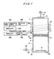
- FIG. 1is a schematic view showing a whole arrangement of a beam processing apparatus according to a first embodiment of the present invention
- FIG. 2Ais a perspective view showing an orifice electrode and a grid electrode in the beam processing apparatus shown in FIG. 1;
- FIG. 2Bis a vertical cross-sectional view partially showing the orifice electrode and the grid electrode shown in FIG. 2A, in which positive ions are being neutralized;
- FIG. 3is a timing chart showing operating states of the beam processing apparatus shown in FIG. 1;
- FIG. 4is a schematic view showing a whole arrangement of a beam processing apparatus according to a modification of the first embodiment of the present invention
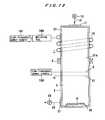
- FIG. 5is a schematic view showing a whole arrangement of a beam processing apparatus according to a second embodiment of the present invention.
- FIG. 6is a timing chart showing operating states of the beam processing apparatus shown in FIG. 5;
- FIG. 7is a schematic view showing a whole arrangement of a beam processing apparatus according to a third embodiment of the present invention.
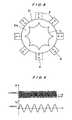
- FIG. 8is a cross-sectional view showing an electron cloud generator in the beam processing apparatus shown in FIG. 7;
- FIG. 9is a timing chart showing operating states of the beam processing apparatus shown in FIG. 7;
- FIG. 10is a schematic view showing a whole arrangement of a beam processing apparatus according to a modification of the third embodiment of the present invention.
- FIG. 11is a schematic view showing a whole arrangement in which positive ions and negative ions are alternately applied to a workpiece without being neutralized in the beam processing apparatus of the first embodiment;
- FIG. 12is a schematic view showing a whole arrangement in which positive ions and negative ions are alternately applied to a workpiece without being neutralized in the beam processing apparatus shown in FIG. 4;
- FIG. 13is a schematic view showing a whole arrangement in which positive ions and negative ions are alternately applied to a workpiece without being neutralized in the beam processing apparatus of the third embodiment;
- FIG. 14is a schematic view showing a whole arrangement in which positive ions and negative ions are alternately applied to a workpiece without being neutralized in the beam processing apparatus shown in FIG. 10;
- FIG. 15is a timing chart showing an example of a voltage to be applied instead of a low-frequency voltage.
- a beam processing apparatusaccording to a first embodiment of the present invention will be described in detail below with reference to FIGS. 1 through 3.
- FIG. 1is a schematic view showing a whole arrangement of a beam processing apparatus according to a first embodiment of the present invention, with electric components in block form.
- the beam processing apparatuscomprises a cylindrical vacuum chamber 3 constituted by a beam generating chamber 1 for generating a neutral particle beam and a process chamber 2 for processing a workpiece X such as a semiconductor substrate, a glass workpiece, an organic workpiece, a ceramic workpiece, or the like.
- the beam generating chamber 1 of the vacuum chamber 3has walls made of quartz glass or ceramics, and the process chamber 2 of the vacuum chamber 3 has walls made of metal.
- the beam generating chamber 1has a coil 10 disposed therearound for inductively coupled plasma (ICP).
- the coil 10is housed in a water-cooled tube having an outside diameter of 8 mm, for example.
- the coil 10of about two turns is wound around the beam generating chamber 1 .
- the coil 10is electrically connected through a matching box 100 to a high-frequency power supply 101 , which applies a high-frequency voltage having a frequency of about 13.56 MHz, for example, to the coil 10 .
- a high-frequency currentis supplied from the high-frequency power supply 101 via the matching box 100 to the coil 10 , an induced magnetic field is produced in the beam generating chamber 1 by the coil 10 .
- the varying magnetic fieldinduces an electric field, which accelerates electrons to generate a plasma in the beam generating chamber 1 .
- the coil 10 , the matching box 100 , and the high-frequency power supply 101constitute a plasma generator for generating a plasma in the beam generating chamber 1 .
- the beam generating chamber 1has a gas inlet port 11 defined in an upper portion thereof for introducing a gas into the beam generating chamber 1 .
- the gas inlet port 11is connected through a gas supply pipe 12 to a gas supply source 13 , which supplies a gas such as SF 6 , CHF 3 , CF 4 , Cl 2 , Ar, O 2 , N 2 , and C 4 F 8 to the beam generating chamber 1 .
- the process chamber 2houses a workpiece holder 20 therein for holding a workpiece X.
- the workpiece Xis placed on an upper surface of the workpiece holder 20 .
- the process chamber 2has a gas outlet port 21 defined in a sidewall thereof for discharging the gas from the process chamber 2 .
- the gas outlet port 21is connected through a gas outlet pipe 22 to a vacuum pump 23 , which operates to maintain the process chamber 2 at a predetermined pressure.
- the orifice electrode 4serves as a first electrode and also serves to neutralize ions.
- a thin-plate grid electrode (second electrode) 5 made of an electrically conductive materialis disposed above the orifice electrode 4 .
- the grid electrode 5is electrically connected to a bipolar power supply (voltage applying unit) 102 , which applies a low-frequency voltage having a frequency of about 400 kHz, for example, to the grid electrode 5 .
- FIG. 2Ais a perspective view showing the orifice electrode 4 and the grid electrode 5
- FIG. 2Bis a vertical cross-sectional view partially showing the orifice electrode 4 and the grid electrode 5 shown in FIG. 2A
- the orifice electrode 4has a number of orifices 4 a defined therein
- the grid electrode 5has a number of grid holes 5 a defined therein.
- the grid electrode 5may comprise a meshed wire, a punching metal, or the like.
- the high-frequency power supply 101 which is connected to the coil 10is connected a modulator 103
- the bipolar power supply 102 which is connected to the grid electrode 5is connected to a modulator 104 .
- the high-frequency power supply 101 and the bipolar power supply 102are connected to each other through the modulators 103 , 104 .
- the application of the voltage by the bipolar power supply 102is synchronized with the application of the voltage by the high-frequency power supply 101 , based on synchronizing signals transmitted between the modulators 103 , 104 .
- FIG. 3is a timing chart showing operating states of the beam processing apparatus shown in FIG. 1.
- Varepresents the potential of the coil 10
- Tethe electron temperature in the beam generating chamber 1
- nethe electron density in the beam generating chamber 1
- ni ⁇the negative ion density in the beam generating chamber 1
- Vbthe potential of the grid electrode 5 .
- the timing chartis schematically shown in FIG. 3, and the shown frequencies are different from the actual frequencies, for example.
- the vacuum pump 23is driven to evacuate the vacuum chamber 3 , and then a gas such as SF 6 , CHF 3 , CF 4 , Cl 2 , Ar, O 2 , N 2 , or C 4 F 8 is introduced from the gas supply source 13 into the beam generating chamber 1 .
- a gassuch as SF 6 , CHF 3 , CF 4 , Cl 2 , Ar, O 2 , N 2 , or C 4 F 8 is introduced from the gas supply source 13 into the beam generating chamber 1 .
- a high-frequency voltage having a frequency of about 13.56 MHzis applied to the coil 10 for 10 microseconds by the high-frequency power supply 101 , so that a high-frequency electric field is produced in the beam generating chamber 1 .
- the gas introduced into the beam generating chamber 1is ionized by electrons that are accelerated by the high-frequency electric field, for thereby generating a high-density plasma in the beam generating chamber 1 .
- the plasmais mainly composed of positive
- the high-frequency voltage applied by the high-frequency power supply 101is interrupted for 100 microseconds. Thereafter, the high-frequency voltage is applied again to the coil 10 for 10 microseconds by the high-frequency power supply 101 to heat the electrons in the plasma in the beam generating chamber 1 . Thus, the above cycle is repeated. In this manner, the application of the high-frequency voltage for 10 microseconds and the interruption of the high-frequency voltage for 100 microseconds are alternately repeated.
- the period of time (100 microseconds) for which the high-frequency voltage is interruptedis sufficiently longer than a period of time in which the electrons in the plasma are attached to the residual process gas to generate negative ions, and sufficiently shorter than a period of time in which the electron density in the plasma is lowered to extinguish the plasma.
- the period of time (10 microseconds) for which the high-frequency voltage is appliedis long enough to recover the energy of the electrons in the plasma which has been lowered during the interruption of the high-frequency voltage.
- Negative ionscan be generated efficiently and continuously by interrupting the high-frequency voltage after the energy of the electrons is increased in the plasma. While ordinary plasmas are mostly composed of positive ions and electrons, the beam processing apparatus according to the present embodiment can efficiently generate a plasma in which positive ions and negative ions coexist therein. Although the high-frequency voltage is interrupted for 100 microseconds in the above example, it may be interrupted for a period of time ranging from 50 to 100 microseconds to generate a large quantity of negative ions as well as positive ions in the plasma.
- a low-frequency voltage having a frequency of about 400 kHzis applied to the grid electrode 5 for 50 microseconds by the bipolar power supply 102 .
- the potential Vb of the grid electrodeis higher than the potential (ground potential) of the orifice electrode 4 (for example, during a period “A” illustrated in FIG. 3)
- a potential differenceis produced between the orifice electrode 4 and the grid electrode 5 so that orifice electrode 4 serves as a cathode and the grid electrode 5 serves as an anode. Therefore, the positive ions 6 (see FIG. 2B) that have passed through the grid electrode 5 toward the orifice electrode 4 are accelerated toward the orifice electrode 4 by the potential difference and introduced into the orifices 4 a defined in the orifice electrode 4 .
- the positive ions 6 that are passing through the orifices 4 a in the orifice electrode 4are collided with the sidewall surfaces of the orifices 4 a and hence neutralized in the vicinity of solid sidewall surfaces of the orifices 4 a , or are collided with gas molecules remaining within the orifices 4 a and hence neutralized by charge exchange with the gas molecules, or are collided with electrons emitted from the surface of the orifice electrode 4 and hence neutralized by recombination with the electrons.
- the positive ions 6are converted into neutral particles 7 (see FIG. 2B).
- the negative and positive ions that have been neutralized when passing through the orifices 4 aare then emitted as an energetic beam into the process chamber 2 .
- the neutral particles 7travel directly in the process chamber 2 and are applied to the workpiece X placed on the workpiece holder 20 , for thereby etching the surface of the workpiece X, cleaning the surface of the workpiece X, modifying (e.g., nitriding or oxidizing) the surface of the workpiece X, or depositing a film on the workpiece X.
- the neutral particles generated by neutralization of the positive ions and the neutral particles generated by neutralization of the negative ionsare alternately applied to the workpiece. Therefore, two types of processes are alternately performed on the workpiece. For example, when gases of Cl 2 and Xe are introduced into the beam generating chamber 1 , the workpiece is sputtered with use of Xe generated by neutralization of the positive ions and etched with use of chlorine generated by neutralization of the negative ions. In this case, the etching rate can be enhanced by chemical sputtering effect.
- a chlorine beamis applied to a workpiece to form thereon several atomic layers in which the chlorine and the workpiece are weakly bonded to each other, and then a Xe beam is applied to the workpiece.
- the energy of the Xe beamis larger than the energy required for removing the atomic layers in which the chlorine and the workpiece are weakly bonded to each other, but is smaller than the energy required for removing the atomic layers in the workpiece which have a large bonding strength
- the Xe beamcan sputter the workpiece to remove only the atomic layers in which the chlorine and the workpiece are weakly bonded to each other.
- the orifice electrode 4serves not only to neutralize the ions, but also to prevent a radiation produced by the plasma from being applied to the workpiece X. Specifically, since the beam generating chamber 1 where the plasma is generated is isolated from the workpiece X by the orifice electrode 4 , the radiation produced by the plasma is not substantially applied to the workpiece X. Therefore, it is possible to reduce adverse effects on the workpiece X due to the radiation such as an ultraviolet ray which would otherwise damage the workpiece X.
- Some charged particlesmay pass through the orifices 4 a in the orifice electrode 4 .
- a deflector or an electron trapmay be disposed downstream of the orifice electrode 4 .
- a voltageis applied to the deflector in a direction perpendicular to a beam traveling direction to change the traveling direction of charged particles, for thereby preventing the charged particles from being applied to the workpiece X.
- the electron trapproduces a magnetic field of about 100 gauss in a direction perpendicular to a beam traveling direction to change the traveling direction of electrons, for thereby preventing the electrons from being applied to the workpiece X.
- the grid electrode 5is positioned downstream of the coil 10 .
- the grid electrodemay be positioned upstream of the coil 10 .
- the grid electrodemay have no grid holes therein.
- FIG. 4is a schematic view showing a whole arrangement of a beam processing apparatus where a grid electrode 50 is disposed upstream of the coil 10 .
- negative ions in a plasma generated in the beam generating chamber 1are accelerated by a voltage applied between the grid electrode 50 and the orifice electrode 4 .
- the orifice electrode and the grid electrodeare used as a neutralization device for neutralizing ions.
- the neutralization deviceis not limited to the illustrated example.
- the present inventionis also applicable to neutralization devices which perform the following processes, for example.
- a neutral gasis introduced into a path of ions extracted from a plasma to form a region of the neutral gas having a high pressure, and the ions are passed through this region for neutralization.
- Ionsare be vibrated by a high-frequency electric field for neutralization.
- a electron cloudis formed in a path of ions extracted from a plasma, and the ions are passed through the electron cloud for neutralization.
- FIG. 5is a schematic view showing a whole arrangement of a beam processing apparatus according to a second embodiment of the present invention, with electric components in block form.
- like parts and componentsare denoted by the same reference numerals and characters as those of the first embodiment and will not be described below.
- the beam processing apparatuscomprises a vacuum chamber 30 made of metal, i.e., a metallic chamber.
- a thin-plate grid electrode (second electrode) 8made of an electrically conductive material is disposed in an upstream end of the vacuum chamber 30 .
- the vacuum chamber 30 and the grid electrode 8are electrically connected to each other and electrically grounded.
- An AC power supply 105 and an AC power supply 106which are connected parallel to each other, are electrically connected to the orifice electrode (a first electrode) 4 .
- the power supplies 105 , 106are also connected to modulators 107 , 108 , respectively.
- the modulator 107 for the AC power supply 105 and the modulator 108 for the AC power supply 106are synchronized with each other by synchronizing signals.
- a voltage applying unitis constituted by the AC power supplies 105 , 106 , and the modulators 107 , 108 .
- the vacuum chamber 30 and the orifice electrode 4are electrically insulated from each other by an insulating material (not shown). The surfaces of the orifice electrode 4 may be covered with dielectric films.
- FIG. 6is a timing chart showing operating states of the beam processing apparatus shown in FIG. 5.
- Vcrepresents the potential of the AC power supply 105
- Tethe electron temperature in the beam generating chamber 1
- nethe electron density in the beam generating chamber 1
- ni ⁇the negative ion density in the beam generating chamber 1
- Vdthe potential of the AC power supply 106
- Vethe potential of the orifice electrode 4 .
- the timing chartis schematically shown in FIG. 6, and the shown frequencies are different from the actual frequencies, for example.
- the vacuum pump 23is driven to evacuate the vacuum chamber 30 , and then a gas is introduced from the gas supply source 13 into the beam generating chamber 1 .
- a high-frequency voltagehaving a frequency of about 13.56 MHz is applied to the orifice electrode 4 for 10 microseconds by the AC power supply 105 , so that a high-frequency electric field is produced in the beam generating chamber 1 .
- the gas introduced into the beam generating chamber 1is ionized by electrons that are accelerated by the high-frequency electric field, for thereby generating a high-density plasma in the beam generating chamber 1 .
- the high-frequency voltage applied by the AC power supply 105is interrupted for 100 microseconds. Thereafter, the high-frequency voltage is applied again to the orifice electrode 4 for 10 microseconds by the AC power supply 105 to heat the electrons in the plasma in the beam generating chamber 1 . Thus, the above cycle is repeated. In this manner, the application of the high-frequency voltage for 10 microseconds and the interruption of the high-frequency voltage for 100 microseconds are alternately repeated.
- Negative ionscan be generated efficiently and continuously by interrupting the high-frequency voltage after the energy of the electrons is increased in the plasma. While ordinary plasmas are mostly composed of positive ions and electrons, the beam processing apparatus according to the present embodiment can efficiently generate a plasma in which positive ions and negative ions coexist therein.
- a low-frequency voltage having a frequency of 400 kHzis applied to the orifice electrode 4 for 50 microseconds by the AC power supply 106 .
- positive and negative ionsare alternately accelerated toward the orifice electrode 4 by the potential differences produced by the low-frequency voltage, and introduced into the orifices 4 a defined in the orifice electrode 4 .
- the beam processing apparatuscan be made compact in structure, and a beam diameter of an energetic beam can be increased inexpensively.
- FIG. 7is a schematic view showing a whole arrangement of a beam processing apparatus according to a third embodiment of the present invention, with electric components in block form.
- like parts and componentsare denoted by the same reference numerals and characters as those of the first embodiment and will not be described below.
- the present embodimentdiffers from the first embodiment in that a beam generating chamber 31 has a negative ion generating chamber 31 a formed downstream of a coil 10 for attaching electrons to a residual gas to generate negative ions.
- the beam processing apparatus in the present embodimentcomprises a downstream beam processing apparatus having a negative ion generating chamber formed downstream of a generated plasma.
- the negative ion generating chamber 31 amay have an electron cloud generator for generating an electron cloud within the negative ion generating chamber 31 a as needed.
- permanent magnets 9are disposed around the negative ion generating chamber 31 a at predetermined circumferential intervals, as shown in FIG. 8.
- the permanent magnets 9are arranged so that the magnetic poles of the adjacent permanent magnets are opposed to each other. With this arrangement, the permanent magnets 9 produce a magnetic field in the negative ion generating chamber 31 a , and electrons in the plasma move along an orbital path C shown in FIG. 8 to form an electron cloud in the negative ion generating chamber 31 a .
- the electron cloud generatorutilizes the permanent magnets 9 .
- the electron cloud generatormay utilize an electric field applied in the negative ion generating chamber 31 .
- the grid electrode 5is electrically connected to a low-frequency power supply 109 , which applies a low-frequency voltage having a frequency of about 400 kHz, for example, to the grid electrode 5 .
- the beam processing apparatushas no modulators, unlike the first embodiment.
- FIG. 9is a timing chart showing operating states of the beam processing apparatus shown in FIG. 7.
- Vfrepresents the potential of the coil 10
- Vgrepresents the potential of the grid electrode 5 .
- the timing chartis schematically shown in FIG. 9, and the shown frequencies are different from the actual frequencies, for example.
- the vacuum pump 23is driven to evacuate the vacuum chamber 3 , and then a gas such as SF 6 , CHF 3 , CF 4 , Cl 2 , Ar, O 2 , or C 4 F 8 is introduced from the gas supply source 13 into the beam generating chamber 31 .
- a gassuch as SF 6 , CHF 3 , CF 4 , Cl 2 , Ar, O 2 , or C 4 F 8 is introduced from the gas supply source 13 into the beam generating chamber 31 .
- a high-frequency voltage having a frequency of about 13.56 MHzis applied to the coil 10 for 10 microseconds by the high-frequency power supply 101 , so that a high-frequency electric field is produced in the beam generating chamber 31 .
- the gas introduced into the beam generating chamber 31is ionized by electrons that are accelerated by the high-frequency electric field, for thereby generating a high-density plasma in the beam generating chamber 31 .
- the plasmais mainly composed of positive ions and heated electrons.
- the negative ion generating chamber 31 ais provided downstream of the plasma.
- electrons lowered in electron temperatureare attached to the residual gas to generate negative ions. Therefore, positive ions, negative ions, and electrons are present in the negative ion generating chamber 31 a.
- a low-frequency voltage having a frequency of about 400 kHzis applied between the grid electrode 5 and the orifice electrode 4 by the low-frequency power supply 109 .
- positive and negative ionsare alternately accelerated toward the orifice electrode 4 by the potential differences produced by the low-frequency voltage, and introduced into the orifices 4 a defined in the orifice electrode 4 .
- FIG. 10is a schematic view showing a whole arrangement of a beam processing apparatus where a grid electrode 50 is disposed upstream of the coil 10 .
- a grid electrode 50is disposed upstream of the coil 10 .
- positive and negative ions in a plasma generated in the beam generating chamber 1are accelerated by a voltage applied between the grid electrode 50 and the orifice electrode 4 .
- positive ions and negative ionsare alternately extracted from a plasma and neutralized.
- positive ions and negative ionsmay alternately be extracted from a plasma and directly applied as a positive ion beam and a negative ion beam to a workpiece without being neutralized.
- FIG. 11is a schematic view showing a whole arrangement in which positive ions and negative ions are alternately applied as a positive ion beam and a negative ion beam to a workpiece X without being neutralized in the beam processing apparatus of the first embodiment.
- a thin-plate grid electrode (second electrode) 51made of an electrically conductive material is disposed instead of the orifice electrode.
- the grid electrode 51is electrically grounded as in the case of the orifice electrode in the first embodiment.
- a high-frequency voltageis applied to a coil 10 for 10 microseconds by the high-frequency power supply 101 to generate a high-density plasma in the beam generating chamber 1 .
- a low-frequency voltageis applied to the grid electrode 5 for 50 microseconds by the bipolar power supply 102 .
- positive ions and negative ionsare alternately emitted from the grid electrode 51 and applied as a positive ion beam and a negative ion beam to the workpiece X.
- FIGS. 12 through 14are schematic views showing a whole arrangement in such cases.
- FIG. 12corresponds to the embodiment shown in FIG. 4, FIG. 13 the third embodiment, and FIG. 14 the embodiment shown in FIG. 10.
- the plasmais generated with use of a coil for ICP.
- the plasmamay be generated with use of an electron cyclotron resonance source (ECR source), a coil for helicon wave plasma, a microwave, or the like.
- ECR sourceelectron cyclotron resonance source
- the frequency of the high-frequency voltageis not limited to 13.56 MHz, but may be in the range from 1 MHz to 20 GHz.
- the frequency of the low-frequency voltageis not limited to 400 kHz.
- a voltage of a rectangular wave as shown in FIG. 15may be applied instead of the low-frequency voltage.
- the present inventionis suitable for use in a beam processing apparatus for generating a highly directional and highly dense particle beam from a high-density plasma and processing a workpiece with the generated particle beam.
Landscapes
- Chemical & Material Sciences (AREA)
- Analytical Chemistry (AREA)
- Physics & Mathematics (AREA)
- Engineering & Computer Science (AREA)
- Plasma & Fusion (AREA)
- Plasma Technology (AREA)
- Drying Of Semiconductors (AREA)
- Physical Or Chemical Processes And Apparatus (AREA)
- Physical Vapour Deposition (AREA)
Abstract
Description
- The present invention relates to a beam processing apparatus, and more particularly to a beam processing apparatus for generating a highly directional and highly dense particle beam from a high-density plasma and processing a workpiece with the generated particle beam.[0001]
- In recent years, semiconductor integrated circuits, information storage media such as hard disks, micromachines, and the like have been processed in highly fine patterns. In the fields of processing such workpieces, attention has been attracted to the use of an energetic beam such as a high-density ion beam which is highly linear, i.e., highly directional, and has a relatively large beam diameter. For example, the energetic beam is applied to a workpiece for depositing a film thereon or etching the workpiece.[0002]
- As beam sources of such energetic beams, there have been used beam generators which generate various kinds of beams including a positive ion beam, a negative ion beam, and a radical beam. The positive ion beam, the negative ion beam, or the radical beam is applied to a desired area of a workpiece from the beam source, for thereby locally depositing a film on the workpiece, etching the workpiece, modifying the surface of the workpiece, or joining or bonding parts of the workpiece.[0003]
- In the case of a beam source which applies charged particles such as positive ions or negative ions to a workpiece, an insulated workpiece cannot be processed because of a charge build-up phenomenon in which electric charges are built up on the workpiece. Further, since the ion beam emitted from the beam source tends to spread due to the space-charge effect, the workpiece cannot be processed in a fine pattern.[0004]
- In order to solve the above problems, there has been proposed a method of introducing electrons into the ion beam to neutralize the electric charges. This method can balance the electric charges on the workpiece on the whole. However, since local unbalance of the electric charges still remains on the workpiece, the workpiece cannot be processed in a fine pattern.[0005]
- In the case where ions are extracted from a plasma source and applied to a workpiece, if a radiation (e.g., an ultraviolet ray) produced by the plasma source is applied to the workpiece, then the radiation adversely affects the workpiece. Thus, it is necessary to shield the workpiece from an adverse radiation (e.g., an ultraviolet ray) emitted from the plasma source.[0006]
- The present invention has been made in view of the above drawbacks. It is therefore an object of the present invention to provide a beam processing apparatus which can apply an energetic beam having a large beam diameter to a workpiece with an inexpensive and compact structure, and can neutralize ions with a high neutralization efficiency to process the workpiece without a charge build-up or damage.[0007]
- According to a first aspect of the present invention, there is provided a beam processing apparatus comprising: a workpiece holder for holding a workpiece; a plasma generator for generating a plasma in a vacuum chamber; a first electrode disposed in the vacuum chamber; a second electrode disposed upstream of the fist electrode in the vacuum chamber; and a voltage applying unit for applying a variable voltage between the first electrode and the second electrode to alternately extract positive ions and negative ions from the plasma generated by the plasma generator.[0008]
- With the above arrangement, positive ions and negative ions can alternately be extracted from a plasma. The extracted positive and negative ions are neutralized and applied as a neutral particle beam to the workpiece, or directly applied as a positive ion beam and a negative ion beam to the workpiece.[0009]
- The plasma generator may generate the plasma by applying a high-frequency electric field. The beam processing apparatus may further comprise a negative ion generating chamber disposed downstream of the plasma generator for attaching electrons to a residual gas to generate negative ions therein. The negative ion generating chamber may have an electron cloud generator for generating an electron cloud within the negative ion generating chamber.[0010]
- According to a second aspect of the present invention, there is provided a beam processing apparatus comprising: a workpiece holder for holding a workpiece; a first electrode disposed in a vacuum chamber; a second electrode disposed upstream of the fist electrode in the vacuum chamber; and a voltage applying unit for applying a variable voltage between the first electrode and the second electrode to generate a plasma between the first electrode and the second electrode and to alternately extract positive ions and negative ions from the generated plasma.[0011]
- With the above arrangement, positive ions and negative ions can alternately be extracted from a plasma. The extracted positive and negative ions are neutralized and applied as a neutral particle beam to the workpiece, or directly applied as a positive ion beam and a negative ion beam to the workpiece. Particularly, the voltage applying unit serves not only to extract the positive ions and the negative ions, but also to generate the plasma. Therefore, it is not necessary to provide a separate plasma generator for generating a plasma. Thus, the beam processing apparatus can be made compact in structure, and a beam diameter of an energetic beam can be increased inexpensively.[0012]
- According to a preferred aspect of the present invention, the beam processing apparatus further comprises a neutralization device for alternately neutralizing the positive ions and the negative ions extracted by the voltage applying unit.[0013]
- With the above arrangement, positive ions and negative ions can alternately be extracted from a plasma. The extracted positive and negative ions are neutralized and applied as a neutral particle beam to the workpiece. Since the workpiece can be processed by the neutral particle beam having no electric charges but having a large translational energy, various processes including an etching process and a deposition process can be performed on the workpiece with high accuracy in such a state that an amount of charge build-up is reduced. Further, the neutral particles generated by neutralization of the positive ions and the neutral particles generated by neutralization of the negative ions are alternately applied to the workpiece. Therefore, two types of processes are alternately performed on the workpiece. For example, when gases of Cl[0014]2and Xe are introduced into the vacuum chamber, the workpiece is sputtered with use of Xe generated by neutralization of the positive ions and etched with use of chlorine generated by neutralization of the negative ions. In this case, the etching rate can be enhanced by chemical sputtering effect. For example, a chlorine beam is applied to a workpiece to form thereon several atomic layers in which the chlorine and the workpiece are weakly bonded to each other, and then a Xe beam is applied to the workpiece. When the energy of the Xe beam is larger than the energy required for removing the atomic layers in which the chlorine and the workpiece are weakly bonded to each other, but is smaller than the energy required for removing the atomic layers in the workpiece which have a large bonding strength, the Xe beam can sputter the workpiece to remove only the atomic layers in which the chlorine and the workpiece are weakly bonded to each other. Thus, when reaction processes are properly selected and the energy of a beam is properly controlled, a workpiece can be etched without defect of the crystal structure of atoms in the workpiece.
- It is desirable that the neutralization device has an orifice electrode as the first electrode and a grid electrode as the second electrode, and the voltage applying unit applies a variable voltage between the orifice electrode and the grid electrode to alternately extract positive ions and negative ions from the plasma and to alternately pass the positive ions and the negative ions through orifices defined in the orifice electrode.[0015]
- With the above arrangement, the voltage applying unit serves not only to extract the positive ions and the negative ions, but also to neutralize the ions. When the orifice electrode is used for neutralizing the positive ions and the negative ions, a high neutralization efficiency can be obtained, and hence a beam diameter of an energetic beam can be increased inexpensively without increasing the size of the apparatus. Further, since the generated plasma is isolated from the workpiece by the orifice electrode, a radiation produced by the plasma is not substantially applied to the workpiece. Therefore, it is possible to reduce adverse effects on the workpiece due to the radiation such as an ultraviolet ray which would otherwise damage the workpiece.[0016]
- The above and other objects, features, and advantages of the present invention will be apparent from the following description when taken in conjunction with the accompanying drawings which illustrates preferred embodiments of the present invention by way of example.[0017]
- FIG. 1 is a schematic view showing a whole arrangement of a beam processing apparatus according to a first embodiment of the present invention;[0018]
- FIG. 2A is a perspective view showing an orifice electrode and a grid electrode in the beam processing apparatus shown in FIG. 1;[0019]
- FIG. 2B is a vertical cross-sectional view partially showing the orifice electrode and the grid electrode shown in FIG. 2A, in which positive ions are being neutralized;[0020]
- FIG. 3 is a timing chart showing operating states of the beam processing apparatus shown in FIG. 1;[0021]
- FIG. 4 is a schematic view showing a whole arrangement of a beam processing apparatus according to a modification of the first embodiment of the present invention;[0022]
- FIG. 5 is a schematic view showing a whole arrangement of a beam processing apparatus according to a second embodiment of the present invention;[0023]
- FIG. 6 is a timing chart showing operating states of the beam processing apparatus shown in FIG. 5;[0024]
- FIG. 7 is a schematic view showing a whole arrangement of a beam processing apparatus according to a third embodiment of the present invention;[0025]
- FIG. 8 is a cross-sectional view showing an electron cloud generator in the beam processing apparatus shown in FIG. 7;[0026]
- FIG. 9 is a timing chart showing operating states of the beam processing apparatus shown in FIG. 7;[0027]
- FIG. 10 is a schematic view showing a whole arrangement of a beam processing apparatus according to a modification of the third embodiment of the present invention;[0028]
- FIG. 11 is a schematic view showing a whole arrangement in which positive ions and negative ions are alternately applied to a workpiece without being neutralized in the beam processing apparatus of the first embodiment;[0029]
- FIG. 12 is a schematic view showing a whole arrangement in which positive ions and negative ions are alternately applied to a workpiece without being neutralized in the beam processing apparatus shown in FIG. 4;[0030]
- FIG. 13 is a schematic view showing a whole arrangement in which positive ions and negative ions are alternately applied to a workpiece without being neutralized in the beam processing apparatus of the third embodiment;[0031]
- FIG. 14 is a schematic view showing a whole arrangement in which positive ions and negative ions are alternately applied to a workpiece without being neutralized in the beam processing apparatus shown in FIG. 10; and[0032]
- FIG. 15 is a timing chart showing an example of a voltage to be applied instead of a low-frequency voltage.[0033]
- A beam processing apparatus according to a first embodiment of the present invention will be described in detail below with reference to FIGS. 1 through 3.[0034]
- FIG. 1 is a schematic view showing a whole arrangement of a beam processing apparatus according to a first embodiment of the present invention, with electric components in block form. As shown in FIG. 1, the beam processing apparatus comprises a[0035]
cylindrical vacuum chamber 3 constituted by abeam generating chamber 1 for generating a neutral particle beam and aprocess chamber 2 for processing a workpiece X such as a semiconductor substrate, a glass workpiece, an organic workpiece, a ceramic workpiece, or the like. Thebeam generating chamber 1 of thevacuum chamber 3 has walls made of quartz glass or ceramics, and theprocess chamber 2 of thevacuum chamber 3 has walls made of metal. - The[0036]
beam generating chamber 1 has acoil 10 disposed therearound for inductively coupled plasma (ICP). Thecoil 10 is housed in a water-cooled tube having an outside diameter of 8 mm, for example. Thecoil 10 of about two turns is wound around thebeam generating chamber 1. Thecoil 10 is electrically connected through amatching box 100 to a high-frequency power supply 101, which applies a high-frequency voltage having a frequency of about 13.56 MHz, for example, to thecoil 10. When a high-frequency current is supplied from the high-frequency power supply 101 via thematching box 100 to thecoil 10, an induced magnetic field is produced in thebeam generating chamber 1 by thecoil 10. The varying magnetic field induces an electric field, which accelerates electrons to generate a plasma in thebeam generating chamber 1. Thus, thecoil 10, thematching box 100, and the high-frequency power supply 101 constitute a plasma generator for generating a plasma in thebeam generating chamber 1. - The[0037]
beam generating chamber 1 has agas inlet port 11 defined in an upper portion thereof for introducing a gas into thebeam generating chamber 1. Thegas inlet port 11 is connected through agas supply pipe 12 to agas supply source 13, which supplies a gas such as SF6, CHF3, CF4, Cl2, Ar, O2, N2, and C4F8to thebeam generating chamber 1. - The[0038]
process chamber 2 houses aworkpiece holder 20 therein for holding a workpiece X. The workpiece X is placed on an upper surface of theworkpiece holder 20. Theprocess chamber 2 has agas outlet port 21 defined in a sidewall thereof for discharging the gas from theprocess chamber 2. Thegas outlet port 21 is connected through agas outlet pipe 22 to avacuum pump 23, which operates to maintain theprocess chamber 2 at a predetermined pressure. - An orifice plate (orifice electrode)[0039]4 made of an electrically conductive material such as graphite is disposed in the lower end of the
beam generating chamber 1 and electrically grounded. Theorifice electrode 4 serves as a first electrode and also serves to neutralize ions. A thin-plate grid electrode (second electrode)5 made of an electrically conductive material is disposed above theorifice electrode 4. Thegrid electrode 5 is electrically connected to a bipolar power supply (voltage applying unit)102, which applies a low-frequency voltage having a frequency of about 400 kHz, for example, to thegrid electrode 5. - FIG. 2A is a perspective view showing the[0040]
orifice electrode 4 and thegrid electrode 5, and FIG. 2B is a vertical cross-sectional view partially showing theorifice electrode 4 and thegrid electrode 5 shown in FIG. 2A. As shown in FIGS. 2A and 2B, theorifice electrode 4 has a number oforifices 4adefined therein, and thegrid electrode 5 has a number ofgrid holes 5adefined therein. Thegrid electrode 5 may comprise a meshed wire, a punching metal, or the like. - The high-[0041]
frequency power supply 101 which is connected to thecoil 10 is connected amodulator 103, and thebipolar power supply 102 which is connected to thegrid electrode 5 is connected to amodulator 104. Thus, the high-frequency power supply 101 and thebipolar power supply 102 are connected to each other through themodulators bipolar power supply 102 is synchronized with the application of the voltage by the high-frequency power supply 101, based on synchronizing signals transmitted between themodulators - Operation of the beam processing apparatus according to the first embodiment will be described below. FIG. 3 is a timing chart showing operating states of the beam processing apparatus shown in FIG. 1. In FIG. 3, Va represents the potential of the[0042]
coil 10, Te the electron temperature in thebeam generating chamber 1, ne the electron density in thebeam generating chamber 1, ni− the negative ion density in thebeam generating chamber 1, and Vb the potential of thegrid electrode 5. The timing chart is schematically shown in FIG. 3, and the shown frequencies are different from the actual frequencies, for example. - The[0043]
vacuum pump 23 is driven to evacuate thevacuum chamber 3, and then a gas such as SF6, CHF3, CF4, Cl2, Ar, O2, N2, or C4F8is introduced from thegas supply source 13 into thebeam generating chamber 1. As shown in FIG. 3, a high-frequency voltage having a frequency of about 13.56 MHz is applied to thecoil 10 for 10 microseconds by the high-frequency power supply 101, so that a high-frequency electric field is produced in thebeam generating chamber 1. The gas introduced into thebeam generating chamber 1 is ionized by electrons that are accelerated by the high-frequency electric field, for thereby generating a high-density plasma in thebeam generating chamber 1. The plasma is mainly composed of positive ions and heated electrons. - Then, the high-frequency voltage applied by the high-[0044]
frequency power supply 101 is interrupted for 100 microseconds. Thereafter, the high-frequency voltage is applied again to thecoil 10 for 10 microseconds by the high-frequency power supply 101 to heat the electrons in the plasma in thebeam generating chamber 1. Thus, the above cycle is repeated. In this manner, the application of the high-frequency voltage for 10 microseconds and the interruption of the high-frequency voltage for 100 microseconds are alternately repeated. The period of time (100 microseconds) for which the high-frequency voltage is interrupted is sufficiently longer than a period of time in which the electrons in the plasma are attached to the residual process gas to generate negative ions, and sufficiently shorter than a period of time in which the electron density in the plasma is lowered to extinguish the plasma. The period of time (10 microseconds) for which the high-frequency voltage is applied is long enough to recover the energy of the electrons in the plasma which has been lowered during the interruption of the high-frequency voltage. - Negative ions can be generated efficiently and continuously by interrupting the high-frequency voltage after the energy of the electrons is increased in the plasma. While ordinary plasmas are mostly composed of positive ions and electrons, the beam processing apparatus according to the present embodiment can efficiently generate a plasma in which positive ions and negative ions coexist therein. Although the high-frequency voltage is interrupted for 100 microseconds in the above example, it may be interrupted for a period of time ranging from 50 to 100 microseconds to generate a large quantity of negative ions as well as positive ions in the plasma.[0045]
- After 50 microseconds from the time when the high-frequency voltage applied by the high-[0046]
frequency power supply 101 is stopped, a low-frequency voltage having a frequency of about 400 kHz is applied to thegrid electrode 5 for 50 microseconds by thebipolar power supply 102. In the application of the low-frequency voltage, when the potential Vb of the grid electrode is higher than the potential (ground potential) of the orifice electrode4 (for example, during a period “A” illustrated in FIG. 3), a potential difference is produced between theorifice electrode 4 and thegrid electrode 5 so thatorifice electrode 4 serves as a cathode and thegrid electrode 5 serves as an anode. Therefore, the positive ions6 (see FIG. 2B) that have passed through thegrid electrode 5 toward theorifice electrode 4 are accelerated toward theorifice electrode 4 by the potential difference and introduced into theorifices 4adefined in theorifice electrode 4. - Most of the[0047]
positive ions 6 that are passing through theorifices 4ain theorifice electrode 4 are collided with the sidewall surfaces of theorifices 4aand hence neutralized in the vicinity of solid sidewall surfaces of theorifices 4a, or are collided with gas molecules remaining within theorifices 4aand hence neutralized by charge exchange with the gas molecules, or are collided with electrons emitted from the surface of theorifice electrode 4 and hence neutralized by recombination with the electrons. Thus, thepositive ions 6 are converted into neutral particles7 (see FIG. 2B). - When the potential Vb of the grid electrode is lower than the potential (ground potential) of the orifice electrode[0048]4 (for example, during a period “B” illustrated in FIG. 3), a potential difference is produced between the
orifice electrode 4 and thegrid electrode 5 so thatorifice electrode 4 serves as an anode and thegrid electrode 5 serves as a cathode. Therefore, the negative ions that have passed through thegrid electrode 5 toward theorifice electrode 4 are accelerated toward theorifice electrode 4 by the potential difference and introduced into theorifices 4adefined in theorifice electrode 4. Most of thenegative ions 6 that are passing through theorifices 4ain theorifice electrode 4 are collided with the sidewall surfaces of theorifices 4aand hence neutralized in the vicinity of solid sidewall surfaces of theorifices 4a, or are collided with gas molecules remaining within theorifices 4aand hence neutralized by charge exchange with the gas molecules. Thus, the negative ions are converted into neutral particles7. - Thus, the negative and positive ions that have been neutralized when passing through the[0049]
orifices 4a, i.e., the neutral particles, are then emitted as an energetic beam into theprocess chamber 2. The neutral particles7 travel directly in theprocess chamber 2 and are applied to the workpiece X placed on theworkpiece holder 20, for thereby etching the surface of the workpiece X, cleaning the surface of the workpiece X, modifying (e.g., nitriding or oxidizing) the surface of the workpiece X, or depositing a film on the workpiece X. - As described above, the neutral particles generated by neutralization of the positive ions and the neutral particles generated by neutralization of the negative ions are alternately applied to the workpiece. Therefore, two types of processes are alternately performed on the workpiece. For example, when gases of Cl[0050]2and Xe are introduced into the
beam generating chamber 1, the workpiece is sputtered with use of Xe generated by neutralization of the positive ions and etched with use of chlorine generated by neutralization of the negative ions. In this case, the etching rate can be enhanced by chemical sputtering effect. - For example, a chlorine beam is applied to a workpiece to form thereon several atomic layers in which the chlorine and the workpiece are weakly bonded to each other, and then a Xe beam is applied to the workpiece. When the energy of the Xe beam is larger than the energy required for removing the atomic layers in which the chlorine and the workpiece are weakly bonded to each other, but is smaller than the energy required for removing the atomic layers in the workpiece which have a large bonding strength, the Xe beam can sputter the workpiece to remove only the atomic layers in which the chlorine and the workpiece are weakly bonded to each other. Thus, when reaction processes are properly selected and the energy of a beam is properly controlled, a workpiece can be etched without destruction of the crystal structure of atoms in the workpiece.[0051]
- The[0052]
orifice electrode 4 serves not only to neutralize the ions, but also to prevent a radiation produced by the plasma from being applied to the workpiece X. Specifically, since thebeam generating chamber 1 where the plasma is generated is isolated from the workpiece X by theorifice electrode 4, the radiation produced by the plasma is not substantially applied to the workpiece X. Therefore, it is possible to reduce adverse effects on the workpiece X due to the radiation such as an ultraviolet ray which would otherwise damage the workpiece X. - Some charged particles may pass through the[0053]
orifices 4ain theorifice electrode 4. In order to prevent such charged particles from being applied to the workpiece X, a deflector or an electron trap may be disposed downstream of theorifice electrode 4. A voltage is applied to the deflector in a direction perpendicular to a beam traveling direction to change the traveling direction of charged particles, for thereby preventing the charged particles from being applied to the workpiece X. The electron trap produces a magnetic field of about 100 gauss in a direction perpendicular to a beam traveling direction to change the traveling direction of electrons, for thereby preventing the electrons from being applied to the workpiece X. - As well known in the art, when an insulated workpiece such as a workpiece made of glass or ceramics is processed, charge build-up may be developed on the surface of the insulated workpiece. However, by applying neutralized particles to the insulating workpiece as described above, various processes including an etching process and a deposition process can be performed on the insulating workpiece with high accuracy in such a state that an amount of charge build-up is reduced. Various types of gases may be introduced into the[0054]
beam generating chamber 1 according to the type of process to be performed on the workpiece X. For example, in a dry etching process, oxygen or a halogen gas may selectively be used according to the kind of the workpiece X. - In the first embodiment, the[0055]
grid electrode 5 is positioned downstream of thecoil 10. However, the grid electrode may be positioned upstream of thecoil 10. In such a case, the grid electrode may have no grid holes therein. FIG. 4 is a schematic view showing a whole arrangement of a beam processing apparatus where agrid electrode 50 is disposed upstream of thecoil 10. In the beam processing apparatus shown in FIG. 4, negative ions in a plasma generated in thebeam generating chamber 1 are accelerated by a voltage applied between thegrid electrode 50 and theorifice electrode 4. - In the first embodiment, the orifice electrode and the grid electrode are used as a neutralization device for neutralizing ions. However, the neutralization device is not limited to the illustrated example. The present invention is also applicable to neutralization devices which perform the following processes, for example.[0056]
- 1) An electron beam is applied to ions extracted from a plasma to neutralize the ions.[0057]
- 2) A neutral gas is introduced into a path of ions extracted from a plasma to form a region of the neutral gas having a high pressure, and the ions are passed through this region for neutralization.[0058]
- 3) A light is applied to ions to neutralize the ions.[0059]
- 4) Ions are be vibrated by a high-frequency electric field for neutralization.[0060]
- 5) A electron cloud is formed in a path of ions extracted from a plasma, and the ions are passed through the electron cloud for neutralization.[0061]
- A beam processing apparatus according to a second embodiment of the present invention will be described below with reference to FIGS. 5 and 6. FIG. 5 is a schematic view showing a whole arrangement of a beam processing apparatus according to a second embodiment of the present invention, with electric components in block form. In FIG. 5, like parts and components are denoted by the same reference numerals and characters as those of the first embodiment and will not be described below.[0062]
- In the present embodiment, the beam processing apparatus comprises a[0063]
vacuum chamber 30 made of metal, i.e., a metallic chamber. As shown in FIG. 5, a thin-plate grid electrode (second electrode)8 made of an electrically conductive material is disposed in an upstream end of thevacuum chamber 30. Thevacuum chamber 30 and thegrid electrode 8 are electrically connected to each other and electrically grounded. - An[0064]
AC power supply 105 and anAC power supply 106, which are connected parallel to each other, are electrically connected to the orifice electrode (a first electrode)4. The power supplies105,106 are also connected to modulators107,108, respectively. Themodulator 107 for theAC power supply 105 and themodulator 108 for theAC power supply 106 are synchronized with each other by synchronizing signals. A voltage applying unit is constituted by the AC power supplies105,106, and themodulators vacuum chamber 30 and theorifice electrode 4 are electrically insulated from each other by an insulating material (not shown). The surfaces of theorifice electrode 4 may be covered with dielectric films. - Operation of the beam processing apparatus according to the second embodiment will be described below. FIG. 6 is a timing chart showing operating states of the beam processing apparatus shown in FIG. 5. In FIG. 6, Vc represents the potential of the[0065]
AC power supply 105, Te the electron temperature in thebeam generating chamber 1, ne the electron density in thebeam generating chamber 1, ni− the negative ion density in thebeam generating chamber 1, Vd the potential of theAC power supply 106, and Ve the potential of theorifice electrode 4. The timing chart is schematically shown in FIG. 6, and the shown frequencies are different from the actual frequencies, for example. - The[0066]
vacuum pump 23 is driven to evacuate thevacuum chamber 30, and then a gas is introduced from thegas supply source 13 into thebeam generating chamber 1. As shown in FIG. 6, a high-frequency voltage having a frequency of about 13.56 MHz is applied to theorifice electrode 4 for 10 microseconds by theAC power supply 105, so that a high-frequency electric field is produced in thebeam generating chamber 1. The gas introduced into thebeam generating chamber 1 is ionized by electrons that are accelerated by the high-frequency electric field, for thereby generating a high-density plasma in thebeam generating chamber 1. - Then, the high-frequency voltage applied by the[0067]
AC power supply 105 is interrupted for 100 microseconds. Thereafter, the high-frequency voltage is applied again to theorifice electrode 4 for 10 microseconds by theAC power supply 105 to heat the electrons in the plasma in thebeam generating chamber 1. Thus, the above cycle is repeated. In this manner, the application of the high-frequency voltage for 10 microseconds and the interruption of the high-frequency voltage for 100 microseconds are alternately repeated. - Negative ions can be generated efficiently and continuously by interrupting the high-frequency voltage after the energy of the electrons is increased in the plasma. While ordinary plasmas are mostly composed of positive ions and electrons, the beam processing apparatus according to the present embodiment can efficiently generate a plasma in which positive ions and negative ions coexist therein.[0068]
- After 50 microseconds from the time when the high-frequency voltage applied by the[0069]
AC power supply 105 is stopped, a low-frequency voltage having a frequency of 400 kHz is applied to theorifice electrode 4 for 50 microseconds by theAC power supply 106. As in the case of the first embodiment, positive and negative ions are alternately accelerated toward theorifice electrode 4 by the potential differences produced by the low-frequency voltage, and introduced into theorifices 4adefined in theorifice electrode 4. - Most of the positive and negative ions that are passing through the[0070]
orifices 4aare alternately neutralized and converted into neutral particles as in the case of the first embodiment. The neutral particles are then emitted as an energetic beam into theprocess chamber 2. The neutral particles travel directly in theprocess chamber 2 and are applied to the workpiece X placed on theworkpiece holder 20. - According to the second embodiment, as described above, by alternately applying the high-frequency voltage and the low-frequency voltage between the[0071]
orifice electrode 4 and thegrid electrode 8, a plasma can be generated in the beam generating chamber, and negative ions can be extracted from the generated plasma. Therefore, it is not necessary to provide a separate plasma generator for generating a plasma. Thus, the beam processing apparatus can be made compact in structure, and a beam diameter of an energetic beam can be increased inexpensively. - A beam processing apparatus according to a third embodiment of the present invention will be described below with reference to FIGS. 7 through 9. FIG. 7 is a schematic view showing a whole arrangement of a beam processing apparatus according to a third embodiment of the present invention, with electric components in block form. In FIG. 7, like parts and components are denoted by the same reference numerals and characters as those of the first embodiment and will not be described below.[0072]
- The present embodiment differs from the first embodiment in that a[0073]
beam generating chamber 31 has a negativeion generating chamber 31aformed downstream of acoil 10 for attaching electrons to a residual gas to generate negative ions. Thus, the beam processing apparatus in the present embodiment comprises a downstream beam processing apparatus having a negative ion generating chamber formed downstream of a generated plasma. - The negative[0074]
ion generating chamber 31amay have an electron cloud generator for generating an electron cloud within the negativeion generating chamber 31aas needed. Specifically,permanent magnets 9 are disposed around the negativeion generating chamber 31aat predetermined circumferential intervals, as shown in FIG. 8. Thepermanent magnets 9 are arranged so that the magnetic poles of the adjacent permanent magnets are opposed to each other. With this arrangement, thepermanent magnets 9 produce a magnetic field in the negativeion generating chamber 31a, and electrons in the plasma move along an orbital path C shown in FIG. 8 to form an electron cloud in the negativeion generating chamber 31a. In the present embodiment, the electron cloud generator utilizes thepermanent magnets 9. However, the electron cloud generator may utilize an electric field applied in the negativeion generating chamber 31. - The[0075]
grid electrode 5 is electrically connected to a low-frequency power supply 109, which applies a low-frequency voltage having a frequency of about 400 kHz, for example, to thegrid electrode 5. In the present embodiment, the beam processing apparatus has no modulators, unlike the first embodiment. - Operation of the beam processing apparatus according to the third embodiment will be described below. FIG. 9 is a timing chart showing operating states of the beam processing apparatus shown in FIG. 7. In FIG. 9, Vf represents the potential of the[0076]
coil 10, and Vg represents the potential of thegrid electrode 5. The timing chart is schematically shown in FIG. 9, and the shown frequencies are different from the actual frequencies, for example. - The[0077]
vacuum pump 23 is driven to evacuate thevacuum chamber 3, and then a gas such as SF6, CHF3, CF4, Cl2, Ar, O2, or C4F8is introduced from thegas supply source 13 into thebeam generating chamber 31. As shown in FIG. 9, a high-frequency voltage having a frequency of about 13.56 MHz is applied to thecoil 10 for 10 microseconds by the high-frequency power supply 101, so that a high-frequency electric field is produced in thebeam generating chamber 31. The gas introduced into thebeam generating chamber 31 is ionized by electrons that are accelerated by the high-frequency electric field, for thereby generating a high-density plasma in thebeam generating chamber 31. The plasma is mainly composed of positive ions and heated electrons. - As described above, in the present embodiment, the negative[0078]
ion generating chamber 31ais provided downstream of the plasma. In the negativeion generating chamber 31a, electrons lowered in electron temperature are attached to the residual gas to generate negative ions. Therefore, positive ions, negative ions, and electrons are present in the negativeion generating chamber 31a. - At the same time when the high-frequency voltage is applied by the high-[0079]
frequency power supply 101, a low-frequency voltage having a frequency of about 400 kHz is applied between thegrid electrode 5 and theorifice electrode 4 by the low-frequency power supply 109. As in the case of the first embodiment, positive and negative ions are alternately accelerated toward theorifice electrode 4 by the potential differences produced by the low-frequency voltage, and introduced into theorifices 4adefined in theorifice electrode 4. - Most of the positive and negative ions that are passing through the[0080]
orifices 4aare alternately neutralized and converted into neutral particles as in the case of the first embodiment. The neutral particles are then emitted as an energetic beam into theprocess chamber 2. The neutral particles travel directly in theprocess chamber 2 and are applied to the workpiece X placed on theworkpiece holder 20. - The grid electrode may be positioned upstream of the[0081]
coil 10. FIG. 10 is a schematic view showing a whole arrangement of a beam processing apparatus where agrid electrode 50 is disposed upstream of thecoil 10. In the beam processing apparatus shown in FIG. 10, positive and negative ions in a plasma generated in thebeam generating chamber 1 are accelerated by a voltage applied between thegrid electrode 50 and theorifice electrode 4. - In the above embodiments, positive ions and negative ions are alternately extracted from a plasma and neutralized. However, positive ions and negative ions may alternately be extracted from a plasma and directly applied as a positive ion beam and a negative ion beam to a workpiece without being neutralized.[0082]
- FIG. 11 is a schematic view showing a whole arrangement in which positive ions and negative ions are alternately applied as a positive ion beam and a negative ion beam to a workpiece X without being neutralized in the beam processing apparatus of the first embodiment. In FIG. 11, a thin-plate grid electrode (second electrode)[0083]51 made of an electrically conductive material is disposed instead of the orifice electrode. The
grid electrode 51 is electrically grounded as in the case of the orifice electrode in the first embodiment. With this arrangement, a high-frequency voltage is applied to acoil 10 for 10 microseconds by the high-frequency power supply 101 to generate a high-density plasma in thebeam generating chamber 1. After 50 microseconds from the time when the high-frequency voltage applied by the high-frequency power supply 101 is stopped, a low-frequency voltage is applied to thegrid electrode 5 for 50 microseconds by thebipolar power supply 102. As in the case of the first embodiment, positive ions and negative ions are alternately emitted from thegrid electrode 51 and applied as a positive ion beam and a negative ion beam to the workpiece X. - In the embodiment shown in FIG. 4, the third embodiment, and the embodiment shown in FIG. 10, positive ions and negative ions may be alternately applied to the workpiece X without being neutralized. FIGS. 12 through 14 are schematic views showing a whole arrangement in such cases. FIG. 12 corresponds to the embodiment shown in FIG. 4, FIG. 13 the third embodiment, and FIG. 14 the embodiment shown in FIG. 10.[0084]
- In the above embodiments, the plasma is generated with use of a coil for ICP. However, the plasma may be generated with use of an electron cyclotron resonance source (ECR source), a coil for helicon wave plasma, a microwave, or the like. The frequency of the high-frequency voltage is not limited to 13.56 MHz, but may be in the range from 1 MHz to 20 GHz. Further, the frequency of the low-frequency voltage is not limited to 400 kHz. For example, a voltage of a rectangular wave as shown in FIG. 15 may be applied instead of the low-frequency voltage.[0085]
- Although certain preferred embodiments of the present invention have been shown and described in detail, it should be understood that various changes and modifications may be made therein without departing from the scope of the appended claims.[0086]
- The present invention is suitable for use in a beam processing apparatus for generating a highly directional and highly dense particle beam from a high-density plasma and processing a workpiece with the generated particle beam.[0087]
Claims (9)
Applications Claiming Priority (3)
| Application Number | Priority Date | Filing Date | Title |
|---|---|---|---|
| JP2001-088863 | 2001-03-26 | ||
| JP2001088863AJP4073174B2 (en) | 2001-03-26 | 2001-03-26 | Neutral particle beam processing equipment |
| PCT/JP2002/002749WO2002078043A2 (en) | 2001-03-26 | 2002-03-22 | Beam processing apparatus |
Publications (2)
| Publication Number | Publication Date |
|---|---|
| US20040108469A1true US20040108469A1 (en) | 2004-06-10 |
| US6849857B2 US6849857B2 (en) | 2005-02-01 |
Family
ID=18943885
Family Applications (1)
| Application Number | Title | Priority Date | Filing Date |
|---|---|---|---|
| US10/471,610Expired - LifetimeUS6849857B2 (en) | 2001-03-26 | 2002-03-22 | Beam processing apparatus |
Country Status (4)
| Country | Link |
|---|---|
| US (1) | US6849857B2 (en) |
| JP (1) | JP4073174B2 (en) |
| AU (1) | AU2002239025A1 (en) |
| WO (1) | WO2002078043A2 (en) |
Cited By (4)
| Publication number | Priority date | Publication date | Assignee | Title |
|---|---|---|---|---|
| US20040094400A1 (en)* | 2001-03-26 | 2004-05-20 | Kasunori Ichiki | Method of processing a surface of a workpiece |
| US20070068624A1 (en)* | 2005-09-28 | 2007-03-29 | Jeon Yun-Kwang | Apparatus to treat a substrate and method thereof |
| WO2023075966A1 (en)* | 2021-10-27 | 2023-05-04 | Applied Materials, Inc. | Ion extraction assembly having variable electrode thickness for beam uniformity control |
| US11694911B2 (en)* | 2016-12-20 | 2023-07-04 | Lam Research Corporation | Systems and methods for metastable activated radical selective strip and etch using dual plenum showerhead |
Families Citing this family (291)
| Publication number | Priority date | Publication date | Assignee | Title |
|---|---|---|---|---|
| FR2858333B1 (en) | 2003-07-31 | 2006-12-08 | Cit Alcatel | METHOD AND DEVICE FOR LOW-AGGRESSIVE DEPOSITION OF PLASMA-ASSISTED VAPOR PHASE DIELECTRIC FILMS |
| US7220943B2 (en)* | 2004-03-26 | 2007-05-22 | Aviza Technology Limted | RF stand offs |
| US20060236931A1 (en)* | 2005-04-25 | 2006-10-26 | Varian Semiconductor Equipment Associates, Inc. | Tilted Plasma Doping |
| US7777197B2 (en)* | 2005-06-02 | 2010-08-17 | Applied Materials, Inc. | Vacuum reaction chamber with x-lamp heater |
| KR100766093B1 (en)* | 2005-07-13 | 2007-10-11 | 삼성전자주식회사 | Neutral beam etching device for separating and accelerating plasma |
| US20070170867A1 (en)* | 2006-01-24 | 2007-07-26 | Varian Semiconductor Equipment Associates, Inc. | Plasma Immersion Ion Source With Low Effective Antenna Voltage |
| GB2437820B (en) | 2006-04-27 | 2011-06-22 | Matsushita Electric Industrial Co Ltd | Fast atom bombardment source, fast atom beam emission method, and surface modification apparatus |
| US7498592B2 (en)* | 2006-06-28 | 2009-03-03 | Wisconsin Alumni Research Foundation | Non-ambipolar radio-frequency plasma electron source and systems and methods for generating electron beams |
| US20080132046A1 (en)* | 2006-12-04 | 2008-06-05 | Varian Semiconductor Equipment Associates, Inc. | Plasma Doping With Electronically Controllable Implant Angle |
| US20080169183A1 (en)* | 2007-01-16 | 2008-07-17 | Varian Semiconductor Equipment Associates, Inc. | Plasma Source with Liner for Reducing Metal Contamination |
| US7820533B2 (en)* | 2007-02-16 | 2010-10-26 | Varian Semiconductor Equipment Associates, Inc. | Multi-step plasma doping with improved dose control |
| FR2965697B1 (en)* | 2010-09-30 | 2014-01-03 | Astrium Sas | METHOD AND DEVICE FOR FORMING A PLASMA BEAM. |
| US20130023129A1 (en) | 2011-07-20 | 2013-01-24 | Asm America, Inc. | Pressure transmitter for a semiconductor processing environment |
| EP2809820A1 (en)* | 2012-02-03 | 2014-12-10 | Seagate Technology LLC | Methods of forming layers |
| US10714315B2 (en) | 2012-10-12 | 2020-07-14 | Asm Ip Holdings B.V. | Semiconductor reaction chamber showerhead |
| US20160376700A1 (en) | 2013-02-01 | 2016-12-29 | Asm Ip Holding B.V. | System for treatment of deposition reactor |
| US11015245B2 (en) | 2014-03-19 | 2021-05-25 | Asm Ip Holding B.V. | Gas-phase reactor and system having exhaust plenum and components thereof |
| FR3020235B1 (en)* | 2014-04-17 | 2016-05-27 | Ecole Polytech | DEVICE FOR FORMING A NEAR-NEUTRAL BEAM OF PARTICLES OF OPPOSED LOADS. |
| US10941490B2 (en) | 2014-10-07 | 2021-03-09 | Asm Ip Holding B.V. | Multiple temperature range susceptor, assembly, reactor and system including the susceptor, and methods of using the same |
| US10276355B2 (en) | 2015-03-12 | 2019-04-30 | Asm Ip Holding B.V. | Multi-zone reactor, system including the reactor, and method of using the same |
| US10458018B2 (en) | 2015-06-26 | 2019-10-29 | Asm Ip Holding B.V. | Structures including metal carbide material, devices including the structures, and methods of forming same |
| US10211308B2 (en) | 2015-10-21 | 2019-02-19 | Asm Ip Holding B.V. | NbMC layers |
| US11139308B2 (en) | 2015-12-29 | 2021-10-05 | Asm Ip Holding B.V. | Atomic layer deposition of III-V compounds to form V-NAND devices |
| US10529554B2 (en) | 2016-02-19 | 2020-01-07 | Asm Ip Holding B.V. | Method for forming silicon nitride film selectively on sidewalls or flat surfaces of trenches |
| US10343920B2 (en) | 2016-03-18 | 2019-07-09 | Asm Ip Holding B.V. | Aligned carbon nanotubes |
| US10367080B2 (en) | 2016-05-02 | 2019-07-30 | Asm Ip Holding B.V. | Method of forming a germanium oxynitride film |
| US11453943B2 (en) | 2016-05-25 | 2022-09-27 | Asm Ip Holding B.V. | Method for forming carbon-containing silicon/metal oxide or nitride film by ALD using silicon precursor and hydrocarbon precursor |
| US9859151B1 (en) | 2016-07-08 | 2018-01-02 | Asm Ip Holding B.V. | Selective film deposition method to form air gaps |
| US10612137B2 (en) | 2016-07-08 | 2020-04-07 | Asm Ip Holdings B.V. | Organic reactants for atomic layer deposition |
| US9887082B1 (en) | 2016-07-28 | 2018-02-06 | Asm Ip Holding B.V. | Method and apparatus for filling a gap |
| US9812320B1 (en) | 2016-07-28 | 2017-11-07 | Asm Ip Holding B.V. | Method and apparatus for filling a gap |
| KR102532607B1 (en) | 2016-07-28 | 2023-05-15 | 에이에스엠 아이피 홀딩 비.브이. | Substrate processing apparatus and method of operating the same |
| US11532757B2 (en) | 2016-10-27 | 2022-12-20 | Asm Ip Holding B.V. | Deposition of charge trapping layers |
| US10714350B2 (en) | 2016-11-01 | 2020-07-14 | ASM IP Holdings, B.V. | Methods for forming a transition metal niobium nitride film on a substrate by atomic layer deposition and related semiconductor device structures |
| KR102546317B1 (en) | 2016-11-15 | 2023-06-21 | 에이에스엠 아이피 홀딩 비.브이. | Gas supply unit and substrate processing apparatus including the same |
| KR102762543B1 (en) | 2016-12-14 | 2025-02-05 | 에이에스엠 아이피 홀딩 비.브이. | Substrate processing apparatus |
| US11447861B2 (en) | 2016-12-15 | 2022-09-20 | Asm Ip Holding B.V. | Sequential infiltration synthesis apparatus and a method of forming a patterned structure |
| US11581186B2 (en) | 2016-12-15 | 2023-02-14 | Asm Ip Holding B.V. | Sequential infiltration synthesis apparatus |
| KR102700194B1 (en) | 2016-12-19 | 2024-08-28 | 에이에스엠 아이피 홀딩 비.브이. | Substrate processing apparatus |
| US10269558B2 (en) | 2016-12-22 | 2019-04-23 | Asm Ip Holding B.V. | Method of forming a structure on a substrate |
| US11390950B2 (en) | 2017-01-10 | 2022-07-19 | Asm Ip Holding B.V. | Reactor system and method to reduce residue buildup during a film deposition process |
| US10468261B2 (en) | 2017-02-15 | 2019-11-05 | Asm Ip Holding B.V. | Methods for forming a metallic film on a substrate by cyclical deposition and related semiconductor device structures |
| JPWO2018173227A1 (en)* | 2017-03-23 | 2019-07-18 | Sppテクノロジーズ株式会社 | Neutral particle beam processing system |
| US10529563B2 (en) | 2017-03-29 | 2020-01-07 | Asm Ip Holdings B.V. | Method for forming doped metal oxide films on a substrate by cyclical deposition and related semiconductor device structures |
| US10770286B2 (en) | 2017-05-08 | 2020-09-08 | Asm Ip Holdings B.V. | Methods for selectively forming a silicon nitride film on a substrate and related semiconductor device structures |
| US12040200B2 (en) | 2017-06-20 | 2024-07-16 | Asm Ip Holding B.V. | Semiconductor processing apparatus and methods for calibrating a semiconductor processing apparatus |
| US11306395B2 (en) | 2017-06-28 | 2022-04-19 | Asm Ip Holding B.V. | Methods for depositing a transition metal nitride film on a substrate by atomic layer deposition and related deposition apparatus |
| KR20190009245A (en) | 2017-07-18 | 2019-01-28 | 에이에스엠 아이피 홀딩 비.브이. | Methods for forming a semiconductor device structure and related semiconductor device structures |
| US11018002B2 (en) | 2017-07-19 | 2021-05-25 | Asm Ip Holding B.V. | Method for selectively depositing a Group IV semiconductor and related semiconductor device structures |
| US10541333B2 (en) | 2017-07-19 | 2020-01-21 | Asm Ip Holding B.V. | Method for depositing a group IV semiconductor and related semiconductor device structures |
| US11374112B2 (en) | 2017-07-19 | 2022-06-28 | Asm Ip Holding B.V. | Method for depositing a group IV semiconductor and related semiconductor device structures |
| US10590535B2 (en) | 2017-07-26 | 2020-03-17 | Asm Ip Holdings B.V. | Chemical treatment, deposition and/or infiltration apparatus and method for using the same |
| TWI815813B (en) | 2017-08-04 | 2023-09-21 | 荷蘭商Asm智慧財產控股公司 | Showerhead assembly for distributing a gas within a reaction chamber |
| US10770336B2 (en) | 2017-08-08 | 2020-09-08 | Asm Ip Holding B.V. | Substrate lift mechanism and reactor including same |
| US10692741B2 (en) | 2017-08-08 | 2020-06-23 | Asm Ip Holdings B.V. | Radiation shield |
| US11769682B2 (en) | 2017-08-09 | 2023-09-26 | Asm Ip Holding B.V. | Storage apparatus for storing cassettes for substrates and processing apparatus equipped therewith |
| US11139191B2 (en) | 2017-08-09 | 2021-10-05 | Asm Ip Holding B.V. | Storage apparatus for storing cassettes for substrates and processing apparatus equipped therewith |
| US11830730B2 (en) | 2017-08-29 | 2023-11-28 | Asm Ip Holding B.V. | Layer forming method and apparatus |
| US11295980B2 (en) | 2017-08-30 | 2022-04-05 | Asm Ip Holding B.V. | Methods for depositing a molybdenum metal film over a dielectric surface of a substrate by a cyclical deposition process and related semiconductor device structures |
| KR102491945B1 (en) | 2017-08-30 | 2023-01-26 | 에이에스엠 아이피 홀딩 비.브이. | Substrate processing apparatus |
| US11056344B2 (en) | 2017-08-30 | 2021-07-06 | Asm Ip Holding B.V. | Layer forming method |
| US10658205B2 (en) | 2017-09-28 | 2020-05-19 | Asm Ip Holdings B.V. | Chemical dispensing apparatus and methods for dispensing a chemical to a reaction chamber |
| US10403504B2 (en) | 2017-10-05 | 2019-09-03 | Asm Ip Holding B.V. | Method for selectively depositing a metallic film on a substrate |
| US10923344B2 (en) | 2017-10-30 | 2021-02-16 | Asm Ip Holding B.V. | Methods for forming a semiconductor structure and related semiconductor structures |
| US11022879B2 (en) | 2017-11-24 | 2021-06-01 | Asm Ip Holding B.V. | Method of forming an enhanced unexposed photoresist layer |
| WO2019103613A1 (en) | 2017-11-27 | 2019-05-31 | Asm Ip Holding B.V. | A storage device for storing wafer cassettes for use with a batch furnace |
| CN111344522B (en) | 2017-11-27 | 2022-04-12 | 阿斯莫Ip控股公司 | Including clean mini-environment device |
| US10872771B2 (en) | 2018-01-16 | 2020-12-22 | Asm Ip Holding B. V. | Method for depositing a material film on a substrate within a reaction chamber by a cyclical deposition process and related device structures |
| KR102695659B1 (en) | 2018-01-19 | 2024-08-14 | 에이에스엠 아이피 홀딩 비.브이. | Method for depositing a gap filling layer by plasma assisted deposition |
| TWI799494B (en) | 2018-01-19 | 2023-04-21 | 荷蘭商Asm 智慧財產控股公司 | Deposition method |
| US11081345B2 (en) | 2018-02-06 | 2021-08-03 | Asm Ip Holding B.V. | Method of post-deposition treatment for silicon oxide film |
| WO2019158960A1 (en) | 2018-02-14 | 2019-08-22 | Asm Ip Holding B.V. | A method for depositing a ruthenium-containing film on a substrate by a cyclical deposition process |
| US10896820B2 (en) | 2018-02-14 | 2021-01-19 | Asm Ip Holding B.V. | Method for depositing a ruthenium-containing film on a substrate by a cyclical deposition process |
| US10731249B2 (en) | 2018-02-15 | 2020-08-04 | Asm Ip Holding B.V. | Method of forming a transition metal containing film on a substrate by a cyclical deposition process, a method for supplying a transition metal halide compound to a reaction chamber, and related vapor deposition apparatus |
| KR102636427B1 (en) | 2018-02-20 | 2024-02-13 | 에이에스엠 아이피 홀딩 비.브이. | Substrate processing method and apparatus |
| US10975470B2 (en) | 2018-02-23 | 2021-04-13 | Asm Ip Holding B.V. | Apparatus for detecting or monitoring for a chemical precursor in a high temperature environment |
| US11473195B2 (en) | 2018-03-01 | 2022-10-18 | Asm Ip Holding B.V. | Semiconductor processing apparatus and a method for processing a substrate |
| US11629406B2 (en) | 2018-03-09 | 2023-04-18 | Asm Ip Holding B.V. | Semiconductor processing apparatus comprising one or more pyrometers for measuring a temperature of a substrate during transfer of the substrate |
| US11114283B2 (en) | 2018-03-16 | 2021-09-07 | Asm Ip Holding B.V. | Reactor, system including the reactor, and methods of manufacturing and using same |
| KR102646467B1 (en) | 2018-03-27 | 2024-03-11 | 에이에스엠 아이피 홀딩 비.브이. | Method of forming an electrode on a substrate and a semiconductor device structure including an electrode |
| US11088002B2 (en) | 2018-03-29 | 2021-08-10 | Asm Ip Holding B.V. | Substrate rack and a substrate processing system and method |
| US11230766B2 (en) | 2018-03-29 | 2022-01-25 | Asm Ip Holding B.V. | Substrate processing apparatus and method |
| KR102600229B1 (en) | 2018-04-09 | 2023-11-10 | 에이에스엠 아이피 홀딩 비.브이. | Substrate supporting device, substrate processing apparatus including the same and substrate processing method |
| TWI811348B (en) | 2018-05-08 | 2023-08-11 | 荷蘭商Asm 智慧財產控股公司 | Methods for depositing an oxide film on a substrate by a cyclical deposition process and related device structures |
| US12025484B2 (en) | 2018-05-08 | 2024-07-02 | Asm Ip Holding B.V. | Thin film forming method |
| US12272527B2 (en) | 2018-05-09 | 2025-04-08 | Asm Ip Holding B.V. | Apparatus for use with hydrogen radicals and method of using same |
| KR102596988B1 (en) | 2018-05-28 | 2023-10-31 | 에이에스엠 아이피 홀딩 비.브이. | Method of processing a substrate and a device manufactured by the same |
| TWI840362B (en) | 2018-06-04 | 2024-05-01 | 荷蘭商Asm Ip私人控股有限公司 | Wafer handling chamber with moisture reduction |
| US11718913B2 (en) | 2018-06-04 | 2023-08-08 | Asm Ip Holding B.V. | Gas distribution system and reactor system including same |
| US11286562B2 (en) | 2018-06-08 | 2022-03-29 | Asm Ip Holding B.V. | Gas-phase chemical reactor and method of using same |
| US10797133B2 (en) | 2018-06-21 | 2020-10-06 | Asm Ip Holding B.V. | Method for depositing a phosphorus doped silicon arsenide film and related semiconductor device structures |
| KR102568797B1 (en) | 2018-06-21 | 2023-08-21 | 에이에스엠 아이피 홀딩 비.브이. | Substrate processing system |
| TWI873894B (en) | 2018-06-27 | 2025-02-21 | 荷蘭商Asm Ip私人控股有限公司 | Cyclic deposition methods for forming metal-containing material and films and structures including the metal-containing material |
| KR102854019B1 (en) | 2018-06-27 | 2025-09-02 | 에이에스엠 아이피 홀딩 비.브이. | Periodic deposition method for forming a metal-containing material and films and structures comprising the metal-containing material |
| US10612136B2 (en) | 2018-06-29 | 2020-04-07 | ASM IP Holding, B.V. | Temperature-controlled flange and reactor system including same |
| US10388513B1 (en) | 2018-07-03 | 2019-08-20 | Asm Ip Holding B.V. | Method for depositing silicon-free carbon-containing film as gap-fill layer by pulse plasma-assisted deposition |
| US10755922B2 (en) | 2018-07-03 | 2020-08-25 | Asm Ip Holding B.V. | Method for depositing silicon-free carbon-containing film as gap-fill layer by pulse plasma-assisted deposition |
| US11053591B2 (en) | 2018-08-06 | 2021-07-06 | Asm Ip Holding B.V. | Multi-port gas injection system and reactor system including same |
| CN109138995B (en)* | 2018-08-13 | 2022-03-01 | 中国石油天然气集团有限公司 | System and method for measuring apparent resistivity while drilling during rotation of drilling tool |
| US11430674B2 (en) | 2018-08-22 | 2022-08-30 | Asm Ip Holding B.V. | Sensor array, apparatus for dispensing a vapor phase reactant to a reaction chamber and related methods |
| KR102707956B1 (en) | 2018-09-11 | 2024-09-19 | 에이에스엠 아이피 홀딩 비.브이. | Method for deposition of a thin film |
| US11024523B2 (en) | 2018-09-11 | 2021-06-01 | Asm Ip Holding B.V. | Substrate processing apparatus and method |
| US11049751B2 (en) | 2018-09-14 | 2021-06-29 | Asm Ip Holding B.V. | Cassette supply system to store and handle cassettes and processing apparatus equipped therewith |
| CN110970344B (en) | 2018-10-01 | 2024-10-25 | Asmip控股有限公司 | Substrate holding apparatus, system comprising the same and method of using the same |
| US11232963B2 (en) | 2018-10-03 | 2022-01-25 | Asm Ip Holding B.V. | Substrate processing apparatus and method |
| KR102592699B1 (en) | 2018-10-08 | 2023-10-23 | 에이에스엠 아이피 홀딩 비.브이. | Substrate support unit and apparatuses for depositing thin film and processing the substrate including the same |
| KR102605121B1 (en) | 2018-10-19 | 2023-11-23 | 에이에스엠 아이피 홀딩 비.브이. | Substrate processing apparatus and substrate processing method |
| KR102546322B1 (en) | 2018-10-19 | 2023-06-21 | 에이에스엠 아이피 홀딩 비.브이. | Substrate processing apparatus and substrate processing method |
| USD948463S1 (en) | 2018-10-24 | 2022-04-12 | Asm Ip Holding B.V. | Susceptor for semiconductor substrate supporting apparatus |
| US12378665B2 (en) | 2018-10-26 | 2025-08-05 | Asm Ip Holding B.V. | High temperature coatings for a preclean and etch apparatus and related methods |
| US11087997B2 (en) | 2018-10-31 | 2021-08-10 | Asm Ip Holding B.V. | Substrate processing apparatus for processing substrates |
| KR102748291B1 (en) | 2018-11-02 | 2024-12-31 | 에이에스엠 아이피 홀딩 비.브이. | Substrate support unit and substrate processing apparatus including the same |
| US11572620B2 (en) | 2018-11-06 | 2023-02-07 | Asm Ip Holding B.V. | Methods for selectively depositing an amorphous silicon film on a substrate |
| US11031242B2 (en) | 2018-11-07 | 2021-06-08 | Asm Ip Holding B.V. | Methods for depositing a boron doped silicon germanium film |
| US10818758B2 (en) | 2018-11-16 | 2020-10-27 | Asm Ip Holding B.V. | Methods for forming a metal silicate film on a substrate in a reaction chamber and related semiconductor device structures |
| US10847366B2 (en) | 2018-11-16 | 2020-11-24 | Asm Ip Holding B.V. | Methods for depositing a transition metal chalcogenide film on a substrate by a cyclical deposition process |
| US12040199B2 (en) | 2018-11-28 | 2024-07-16 | Asm Ip Holding B.V. | Substrate processing apparatus for processing substrates |
| US11217444B2 (en) | 2018-11-30 | 2022-01-04 | Asm Ip Holding B.V. | Method for forming an ultraviolet radiation responsive metal oxide-containing film |
| KR102636428B1 (en) | 2018-12-04 | 2024-02-13 | 에이에스엠 아이피 홀딩 비.브이. | A method for cleaning a substrate processing apparatus |
| US11158513B2 (en) | 2018-12-13 | 2021-10-26 | Asm Ip Holding B.V. | Methods for forming a rhenium-containing film on a substrate by a cyclical deposition process and related semiconductor device structures |
| TWI874340B (en) | 2018-12-14 | 2025-03-01 | 荷蘭商Asm Ip私人控股有限公司 | Method of forming device structure, structure formed by the method and system for performing the method |
| TWI866480B (en) | 2019-01-17 | 2024-12-11 | 荷蘭商Asm Ip 私人控股有限公司 | Methods of forming a transition metal containing film on a substrate by a cyclical deposition process |
| KR102727227B1 (en) | 2019-01-22 | 2024-11-07 | 에이에스엠 아이피 홀딩 비.브이. | Semiconductor processing device |
| CN111524788B (en) | 2019-02-01 | 2023-11-24 | Asm Ip私人控股有限公司 | Method for forming topologically selective films of silicon oxide |
| TWI845607B (en) | 2019-02-20 | 2024-06-21 | 荷蘭商Asm Ip私人控股有限公司 | Cyclical deposition method and apparatus for filling a recess formed within a substrate surface |
| TWI838458B (en) | 2019-02-20 | 2024-04-11 | 荷蘭商Asm Ip私人控股有限公司 | Apparatus and methods for plug fill deposition in 3-d nand applications |
| KR102626263B1 (en) | 2019-02-20 | 2024-01-16 | 에이에스엠 아이피 홀딩 비.브이. | Cyclical deposition method including treatment step and apparatus for same |
| TWI873122B (en) | 2019-02-20 | 2025-02-21 | 荷蘭商Asm Ip私人控股有限公司 | Method of filling a recess formed within a surface of a substrate, semiconductor structure formed according to the method, and semiconductor processing apparatus |
| TWI842826B (en) | 2019-02-22 | 2024-05-21 | 荷蘭商Asm Ip私人控股有限公司 | Substrate processing apparatus and method for processing substrate |
| KR102782593B1 (en) | 2019-03-08 | 2025-03-14 | 에이에스엠 아이피 홀딩 비.브이. | Structure Including SiOC Layer and Method of Forming Same |
| US11742198B2 (en) | 2019-03-08 | 2023-08-29 | Asm Ip Holding B.V. | Structure including SiOCN layer and method of forming same |
| KR102858005B1 (en) | 2019-03-08 | 2025-09-09 | 에이에스엠 아이피 홀딩 비.브이. | Method for Selective Deposition of Silicon Nitride Layer and Structure Including Selectively-Deposited Silicon Nitride Layer |
| JP2020167398A (en) | 2019-03-28 | 2020-10-08 | エーエスエム・アイピー・ホールディング・ベー・フェー | Door openers and substrate processing equipment provided with door openers |
| KR102809999B1 (en) | 2019-04-01 | 2025-05-19 | 에이에스엠 아이피 홀딩 비.브이. | Method of manufacturing semiconductor device |
| KR20200123380A (en) | 2019-04-19 | 2020-10-29 | 에이에스엠 아이피 홀딩 비.브이. | Layer forming method and apparatus |
| KR20200125453A (en) | 2019-04-24 | 2020-11-04 | 에이에스엠 아이피 홀딩 비.브이. | Gas-phase reactor system and method of using same |
| KR20200130121A (en) | 2019-05-07 | 2020-11-18 | 에이에스엠 아이피 홀딩 비.브이. | Chemical source vessel with dip tube |
| US11289326B2 (en) | 2019-05-07 | 2022-03-29 | Asm Ip Holding B.V. | Method for reforming amorphous carbon polymer film |
| KR20200130652A (en) | 2019-05-10 | 2020-11-19 | 에이에스엠 아이피 홀딩 비.브이. | Method of depositing material onto a surface and structure formed according to the method |
| JP7612342B2 (en) | 2019-05-16 | 2025-01-14 | エーエスエム・アイピー・ホールディング・ベー・フェー | Wafer boat handling apparatus, vertical batch furnace and method |
| JP7598201B2 (en) | 2019-05-16 | 2024-12-11 | エーエスエム・アイピー・ホールディング・ベー・フェー | Wafer boat handling apparatus, vertical batch furnace and method |
| USD947913S1 (en) | 2019-05-17 | 2022-04-05 | Asm Ip Holding B.V. | Susceptor shaft |
| USD975665S1 (en) | 2019-05-17 | 2023-01-17 | Asm Ip Holding B.V. | Susceptor shaft |
| USD935572S1 (en) | 2019-05-24 | 2021-11-09 | Asm Ip Holding B.V. | Gas channel plate |
| USD922229S1 (en) | 2019-06-05 | 2021-06-15 | Asm Ip Holding B.V. | Device for controlling a temperature of a gas supply unit |
| KR20200141002A (en) | 2019-06-06 | 2020-12-17 | 에이에스엠 아이피 홀딩 비.브이. | Method of using a gas-phase reactor system including analyzing exhausted gas |
| KR20200141931A (en) | 2019-06-10 | 2020-12-21 | 에이에스엠 아이피 홀딩 비.브이. | Method for cleaning quartz epitaxial chambers |
| KR20200143254A (en) | 2019-06-11 | 2020-12-23 | 에이에스엠 아이피 홀딩 비.브이. | Method of forming an electronic structure using an reforming gas, system for performing the method, and structure formed using the method |
| USD944946S1 (en) | 2019-06-14 | 2022-03-01 | Asm Ip Holding B.V. | Shower plate |
| USD931978S1 (en) | 2019-06-27 | 2021-09-28 | Asm Ip Holding B.V. | Showerhead vacuum transport |
| KR20210005515A (en) | 2019-07-03 | 2021-01-14 | 에이에스엠 아이피 홀딩 비.브이. | Temperature control assembly for substrate processing apparatus and method of using same |
| JP7499079B2 (en) | 2019-07-09 | 2024-06-13 | エーエスエム・アイピー・ホールディング・ベー・フェー | Plasma device using coaxial waveguide and substrate processing method |
| CN112216646A (en) | 2019-07-10 | 2021-01-12 | Asm Ip私人控股有限公司 | Substrate supporting assembly and substrate processing device comprising same |
| KR20210010307A (en) | 2019-07-16 | 2021-01-27 | 에이에스엠 아이피 홀딩 비.브이. | Substrate processing apparatus |
| KR20210010816A (en) | 2019-07-17 | 2021-01-28 | 에이에스엠 아이피 홀딩 비.브이. | Radical assist ignition plasma system and method |
| KR102860110B1 (en) | 2019-07-17 | 2025-09-16 | 에이에스엠 아이피 홀딩 비.브이. | Methods of forming silicon germanium structures |
| US11643724B2 (en) | 2019-07-18 | 2023-05-09 | Asm Ip Holding B.V. | Method of forming structures using a neutral beam |
| KR20210010817A (en) | 2019-07-19 | 2021-01-28 | 에이에스엠 아이피 홀딩 비.브이. | Method of Forming Topology-Controlled Amorphous Carbon Polymer Film |
| TWI839544B (en) | 2019-07-19 | 2024-04-21 | 荷蘭商Asm Ip私人控股有限公司 | Method of forming topology-controlled amorphous carbon polymer film |
| TWI851767B (en) | 2019-07-29 | 2024-08-11 | 荷蘭商Asm Ip私人控股有限公司 | Methods for selective deposition utilizing n-type dopants and/or alternative dopants to achieve high dopant incorporation |
| CN112309899A (en) | 2019-07-30 | 2021-02-02 | Asm Ip私人控股有限公司 | Substrate processing apparatus |
| US12169361B2 (en) | 2019-07-30 | 2024-12-17 | Asm Ip Holding B.V. | Substrate processing apparatus and method |
| CN112309900A (en) | 2019-07-30 | 2021-02-02 | Asm Ip私人控股有限公司 | Substrate processing apparatus |
| US11587814B2 (en) | 2019-07-31 | 2023-02-21 | Asm Ip Holding B.V. | Vertical batch furnace assembly |
| US11227782B2 (en) | 2019-07-31 | 2022-01-18 | Asm Ip Holding B.V. | Vertical batch furnace assembly |
| US11587815B2 (en) | 2019-07-31 | 2023-02-21 | Asm Ip Holding B.V. | Vertical batch furnace assembly |
| CN112323048B (en) | 2019-08-05 | 2024-02-09 | Asm Ip私人控股有限公司 | Liquid level sensor for chemical source container |
| CN112342526A (en) | 2019-08-09 | 2021-02-09 | Asm Ip私人控股有限公司 | Heater assembly including cooling device and method of using same |
| USD965524S1 (en) | 2019-08-19 | 2022-10-04 | Asm Ip Holding B.V. | Susceptor support |
| USD965044S1 (en) | 2019-08-19 | 2022-09-27 | Asm Ip Holding B.V. | Susceptor shaft |
| JP2021031769A (en) | 2019-08-21 | 2021-03-01 | エーエスエム アイピー ホールディング ビー.ブイ. | Production apparatus of mixed gas of film deposition raw material and film deposition apparatus |
| USD979506S1 (en) | 2019-08-22 | 2023-02-28 | Asm Ip Holding B.V. | Insulator |
| KR20210024423A (en) | 2019-08-22 | 2021-03-05 | 에이에스엠 아이피 홀딩 비.브이. | Method for forming a structure with a hole |
| USD949319S1 (en) | 2019-08-22 | 2022-04-19 | Asm Ip Holding B.V. | Exhaust duct |
| USD930782S1 (en) | 2019-08-22 | 2021-09-14 | Asm Ip Holding B.V. | Gas distributor |
| USD940837S1 (en) | 2019-08-22 | 2022-01-11 | Asm Ip Holding B.V. | Electrode |
| US11286558B2 (en) | 2019-08-23 | 2022-03-29 | Asm Ip Holding B.V. | Methods for depositing a molybdenum nitride film on a surface of a substrate by a cyclical deposition process and related semiconductor device structures including a molybdenum nitride film |
| KR20210024420A (en) | 2019-08-23 | 2021-03-05 | 에이에스엠 아이피 홀딩 비.브이. | Method for depositing silicon oxide film having improved quality by peald using bis(diethylamino)silane |
| KR102806450B1 (en) | 2019-09-04 | 2025-05-12 | 에이에스엠 아이피 홀딩 비.브이. | Methods for selective deposition using a sacrificial capping layer |
| KR102733104B1 (en) | 2019-09-05 | 2024-11-22 | 에이에스엠 아이피 홀딩 비.브이. | Substrate processing apparatus |
| US11562901B2 (en) | 2019-09-25 | 2023-01-24 | Asm Ip Holding B.V. | Substrate processing method |
| CN112593212B (en) | 2019-10-02 | 2023-12-22 | Asm Ip私人控股有限公司 | Method for forming topologically selective silicon oxide film by cyclic plasma enhanced deposition process |
| TWI846953B (en) | 2019-10-08 | 2024-07-01 | 荷蘭商Asm Ip私人控股有限公司 | Substrate processing device |
| TW202128273A (en) | 2019-10-08 | 2021-08-01 | 荷蘭商Asm Ip私人控股有限公司 | Gas injection system, reactor system, and method of depositing material on surface of substratewithin reaction chamber |
| KR20210042810A (en) | 2019-10-08 | 2021-04-20 | 에이에스엠 아이피 홀딩 비.브이. | Reactor system including a gas distribution assembly for use with activated species and method of using same |
| TWI846966B (en) | 2019-10-10 | 2024-07-01 | 荷蘭商Asm Ip私人控股有限公司 | Method of forming a photoresist underlayer and structure including same |
| US12009241B2 (en) | 2019-10-14 | 2024-06-11 | Asm Ip Holding B.V. | Vertical batch furnace assembly with detector to detect cassette |
| TWI834919B (en) | 2019-10-16 | 2024-03-11 | 荷蘭商Asm Ip私人控股有限公司 | Method of topology-selective film formation of silicon oxide |
| US11637014B2 (en) | 2019-10-17 | 2023-04-25 | Asm Ip Holding B.V. | Methods for selective deposition of doped semiconductor material |
| KR102845724B1 (en) | 2019-10-21 | 2025-08-13 | 에이에스엠 아이피 홀딩 비.브이. | Apparatus and methods for selectively etching films |
| KR20210050453A (en) | 2019-10-25 | 2021-05-07 | 에이에스엠 아이피 홀딩 비.브이. | Methods for filling a gap feature on a substrate surface and related semiconductor structures |
| US11646205B2 (en) | 2019-10-29 | 2023-05-09 | Asm Ip Holding B.V. | Methods of selectively forming n-type doped material on a surface, systems for selectively forming n-type doped material, and structures formed using same |
| KR20210054983A (en) | 2019-11-05 | 2021-05-14 | 에이에스엠 아이피 홀딩 비.브이. | Structures with doped semiconductor layers and methods and systems for forming same |
| US11501968B2 (en) | 2019-11-15 | 2022-11-15 | Asm Ip Holding B.V. | Method for providing a semiconductor device with silicon filled gaps |
| KR102861314B1 (en) | 2019-11-20 | 2025-09-17 | 에이에스엠 아이피 홀딩 비.브이. | Method of depositing carbon-containing material on a surface of a substrate, structure formed using the method, and system for forming the structure |
| CN112951697B (en) | 2019-11-26 | 2025-07-29 | Asmip私人控股有限公司 | Substrate processing apparatus |
| US11450529B2 (en) | 2019-11-26 | 2022-09-20 | Asm Ip Holding B.V. | Methods for selectively forming a target film on a substrate comprising a first dielectric surface and a second metallic surface |
| CN112885692B (en) | 2019-11-29 | 2025-08-15 | Asmip私人控股有限公司 | Substrate processing apparatus |
| CN120432376A (en) | 2019-11-29 | 2025-08-05 | Asm Ip私人控股有限公司 | Substrate processing apparatus |
| JP7527928B2 (en) | 2019-12-02 | 2024-08-05 | エーエスエム・アイピー・ホールディング・ベー・フェー | Substrate processing apparatus and substrate processing method |
| KR20210070898A (en) | 2019-12-04 | 2021-06-15 | 에이에스엠 아이피 홀딩 비.브이. | Substrate processing apparatus |
| KR20210078405A (en) | 2019-12-17 | 2021-06-28 | 에이에스엠 아이피 홀딩 비.브이. | Method of forming vanadium nitride layer and structure including the vanadium nitride layer |
| KR20210080214A (en) | 2019-12-19 | 2021-06-30 | 에이에스엠 아이피 홀딩 비.브이. | Methods for filling a gap feature on a substrate and related semiconductor structures |
| JP7730637B2 (en) | 2020-01-06 | 2025-08-28 | エーエスエム・アイピー・ホールディング・ベー・フェー | Gas delivery assembly, components thereof, and reactor system including same |
| JP7636892B2 (en) | 2020-01-06 | 2025-02-27 | エーエスエム・アイピー・ホールディング・ベー・フェー | Channeled Lift Pins |
| US11993847B2 (en) | 2020-01-08 | 2024-05-28 | Asm Ip Holding B.V. | Injector |
| KR20210093163A (en) | 2020-01-16 | 2021-07-27 | 에이에스엠 아이피 홀딩 비.브이. | Method of forming high aspect ratio features |
| KR102675856B1 (en) | 2020-01-20 | 2024-06-17 | 에이에스엠 아이피 홀딩 비.브이. | Method of forming thin film and method of modifying surface of thin film |
| TWI889744B (en) | 2020-01-29 | 2025-07-11 | 荷蘭商Asm Ip私人控股有限公司 | Contaminant trap system, and baffle plate stack |
| TW202513845A (en) | 2020-02-03 | 2025-04-01 | 荷蘭商Asm Ip私人控股有限公司 | Semiconductor structures and methods for forming the same |
| KR20210100010A (en) | 2020-02-04 | 2021-08-13 | 에이에스엠 아이피 홀딩 비.브이. | Method and apparatus for transmittance measurements of large articles |
| US11776846B2 (en) | 2020-02-07 | 2023-10-03 | Asm Ip Holding B.V. | Methods for depositing gap filling fluids and related systems and devices |
| KR20210103956A (en) | 2020-02-13 | 2021-08-24 | 에이에스엠 아이피 홀딩 비.브이. | Substrate processing apparatus including light receiving device and calibration method of light receiving device |
| TW202146691A (en) | 2020-02-13 | 2021-12-16 | 荷蘭商Asm Ip私人控股有限公司 | Gas distribution assembly, shower plate assembly, and method of adjusting conductance of gas to reaction chamber |
| TWI855223B (en) | 2020-02-17 | 2024-09-11 | 荷蘭商Asm Ip私人控股有限公司 | Method for growing phosphorous-doped silicon layer |
| CN113410160A (en) | 2020-02-28 | 2021-09-17 | Asm Ip私人控股有限公司 | System specially used for cleaning parts |
| KR20210113043A (en) | 2020-03-04 | 2021-09-15 | 에이에스엠 아이피 홀딩 비.브이. | Alignment fixture for a reactor system |
| KR20210116240A (en) | 2020-03-11 | 2021-09-27 | 에이에스엠 아이피 홀딩 비.브이. | Substrate handling device with adjustable joints |
| US11876356B2 (en) | 2020-03-11 | 2024-01-16 | Asm Ip Holding B.V. | Lockout tagout assembly and system and method of using same |
| KR102775390B1 (en) | 2020-03-12 | 2025-02-28 | 에이에스엠 아이피 홀딩 비.브이. | Method for Fabricating Layer Structure Having Target Topological Profile |
| US12173404B2 (en) | 2020-03-17 | 2024-12-24 | Asm Ip Holding B.V. | Method of depositing epitaxial material, structure formed using the method, and system for performing the method |
| JP7404119B2 (en)* | 2020-03-19 | 2023-12-25 | 住友重機械工業株式会社 | Negative ion generator |
| KR102755229B1 (en) | 2020-04-02 | 2025-01-14 | 에이에스엠 아이피 홀딩 비.브이. | Thin film forming method |
| TWI887376B (en) | 2020-04-03 | 2025-06-21 | 荷蘭商Asm Ip私人控股有限公司 | Method for manufacturing semiconductor device |
| TWI888525B (en) | 2020-04-08 | 2025-07-01 | 荷蘭商Asm Ip私人控股有限公司 | Apparatus and methods for selectively etching silcon oxide films |
| US11821078B2 (en) | 2020-04-15 | 2023-11-21 | Asm Ip Holding B.V. | Method for forming precoat film and method for forming silicon-containing film |
| KR20210128343A (en) | 2020-04-15 | 2021-10-26 | 에이에스엠 아이피 홀딩 비.브이. | Method of forming chromium nitride layer and structure including the chromium nitride layer |
| US11996289B2 (en) | 2020-04-16 | 2024-05-28 | Asm Ip Holding B.V. | Methods of forming structures including silicon germanium and silicon layers, devices formed using the methods, and systems for performing the methods |
| KR20210130646A (en) | 2020-04-21 | 2021-11-01 | 에이에스엠 아이피 홀딩 비.브이. | Method for processing a substrate |
| KR102866804B1 (en) | 2020-04-24 | 2025-09-30 | 에이에스엠 아이피 홀딩 비.브이. | Vertical batch furnace assembly comprising a cooling gas supply |
| KR20210132600A (en) | 2020-04-24 | 2021-11-04 | 에이에스엠 아이피 홀딩 비.브이. | Methods and systems for depositing a layer comprising vanadium, nitrogen, and a further element |
| KR20210132612A (en) | 2020-04-24 | 2021-11-04 | 에이에스엠 아이피 홀딩 비.브이. | Methods and apparatus for stabilizing vanadium compounds |
| TW202208671A (en) | 2020-04-24 | 2022-03-01 | 荷蘭商Asm Ip私人控股有限公司 | Methods of forming structures including vanadium boride and vanadium phosphide layers |
| CN113555279A (en) | 2020-04-24 | 2021-10-26 | Asm Ip私人控股有限公司 | Methods of forming vanadium nitride-containing layers and structures comprising the same |
| KR102783898B1 (en) | 2020-04-29 | 2025-03-18 | 에이에스엠 아이피 홀딩 비.브이. | Solid source precursor vessel |
| KR20210134869A (en) | 2020-05-01 | 2021-11-11 | 에이에스엠 아이피 홀딩 비.브이. | Fast FOUP swapping with a FOUP handler |
| JP7726664B2 (en) | 2020-05-04 | 2025-08-20 | エーエスエム・アイピー・ホールディング・ベー・フェー | Substrate processing system for processing a substrate |
| KR102788543B1 (en) | 2020-05-13 | 2025-03-27 | 에이에스엠 아이피 홀딩 비.브이. | Laser alignment fixture for a reactor system |
| TW202146699A (en) | 2020-05-15 | 2021-12-16 | 荷蘭商Asm Ip私人控股有限公司 | Method of forming a silicon germanium layer, semiconductor structure, semiconductor device, method of forming a deposition layer, and deposition system |
| KR20210143653A (en) | 2020-05-19 | 2021-11-29 | 에이에스엠 아이피 홀딩 비.브이. | Substrate processing apparatus |
| KR20210145079A (en) | 2020-05-21 | 2021-12-01 | 에이에스엠 아이피 홀딩 비.브이. | Flange and apparatus for processing substrates |
| KR102795476B1 (en) | 2020-05-21 | 2025-04-11 | 에이에스엠 아이피 홀딩 비.브이. | Structures including multiple carbon layers and methods of forming and using same |
| TWI873343B (en) | 2020-05-22 | 2025-02-21 | 荷蘭商Asm Ip私人控股有限公司 | Reaction system for forming thin film on substrate |
| KR20210146802A (en) | 2020-05-26 | 2021-12-06 | 에이에스엠 아이피 홀딩 비.브이. | Method for depositing boron and gallium containing silicon germanium layers |
| TWI876048B (en) | 2020-05-29 | 2025-03-11 | 荷蘭商Asm Ip私人控股有限公司 | Substrate processing device |
| TW202212620A (en) | 2020-06-02 | 2022-04-01 | 荷蘭商Asm Ip私人控股有限公司 | Apparatus for processing substrate, method of forming film, and method of controlling apparatus for processing substrate |
| TW202208659A (en) | 2020-06-16 | 2022-03-01 | 荷蘭商Asm Ip私人控股有限公司 | Method for depositing boron containing silicon germanium layers |
| TW202218133A (en) | 2020-06-24 | 2022-05-01 | 荷蘭商Asm Ip私人控股有限公司 | Method for forming a layer provided with silicon |
| TWI873359B (en) | 2020-06-30 | 2025-02-21 | 荷蘭商Asm Ip私人控股有限公司 | Substrate processing method |
| US12431354B2 (en) | 2020-07-01 | 2025-09-30 | Asm Ip Holding B.V. | Silicon nitride and silicon oxide deposition methods using fluorine inhibitor |
| TW202202649A (en) | 2020-07-08 | 2022-01-16 | 荷蘭商Asm Ip私人控股有限公司 | Substrate processing method |
| KR20220010438A (en) | 2020-07-17 | 2022-01-25 | 에이에스엠 아이피 홀딩 비.브이. | Structures and methods for use in photolithography |
| TWI878570B (en) | 2020-07-20 | 2025-04-01 | 荷蘭商Asm Ip私人控股有限公司 | Method and system for depositing molybdenum layers |
| KR20220011092A (en) | 2020-07-20 | 2022-01-27 | 에이에스엠 아이피 홀딩 비.브이. | Method and system for forming structures including transition metal layers |
| US12322591B2 (en) | 2020-07-27 | 2025-06-03 | Asm Ip Holding B.V. | Thin film deposition process |
| KR20220021863A (en) | 2020-08-14 | 2022-02-22 | 에이에스엠 아이피 홀딩 비.브이. | Method for processing a substrate |
| US12040177B2 (en) | 2020-08-18 | 2024-07-16 | Asm Ip Holding B.V. | Methods for forming a laminate film by cyclical plasma-enhanced deposition processes |
| TW202228863A (en) | 2020-08-25 | 2022-08-01 | 荷蘭商Asm Ip私人控股有限公司 | Method for cleaning a substrate, method for selectively depositing, and reaction system |
| US11521834B2 (en)* | 2020-08-26 | 2022-12-06 | Tokyo Electron Limited | Plasma processing systems and methods for chemical processing a substrate |
| US11725280B2 (en) | 2020-08-26 | 2023-08-15 | Asm Ip Holding B.V. | Method for forming metal silicon oxide and metal silicon oxynitride layers |
| TW202229601A (en) | 2020-08-27 | 2022-08-01 | 荷蘭商Asm Ip私人控股有限公司 | Method of forming patterned structures, method of manipulating mechanical property, device structure, and substrate processing system |
| TW202217045A (en) | 2020-09-10 | 2022-05-01 | 荷蘭商Asm Ip私人控股有限公司 | Methods for depositing gap filing fluids and related systems and devices |
| USD990534S1 (en) | 2020-09-11 | 2023-06-27 | Asm Ip Holding B.V. | Weighted lift pin |
| KR20220036866A (en) | 2020-09-16 | 2022-03-23 | 에이에스엠 아이피 홀딩 비.브이. | Silicon oxide deposition method |
| USD1012873S1 (en) | 2020-09-24 | 2024-01-30 | Asm Ip Holding B.V. | Electrode for semiconductor processing apparatus |
| TWI889903B (en) | 2020-09-25 | 2025-07-11 | 荷蘭商Asm Ip私人控股有限公司 | Semiconductor processing method |
| US12009224B2 (en) | 2020-09-29 | 2024-06-11 | Asm Ip Holding B.V. | Apparatus and method for etching metal nitrides |
| KR20220045900A (en) | 2020-10-06 | 2022-04-13 | 에이에스엠 아이피 홀딩 비.브이. | Deposition method and an apparatus for depositing a silicon-containing material |
| CN114293174A (en) | 2020-10-07 | 2022-04-08 | Asm Ip私人控股有限公司 | Gas supply unit and substrate processing apparatus including the same |
| TW202229613A (en) | 2020-10-14 | 2022-08-01 | 荷蘭商Asm Ip私人控股有限公司 | Method of depositing material on stepped structure |
| TW202232565A (en) | 2020-10-15 | 2022-08-16 | 荷蘭商Asm Ip私人控股有限公司 | Method of manufacturing semiconductor device, and substrate treatment apparatus using ether-cat |
| TW202217037A (en) | 2020-10-22 | 2022-05-01 | 荷蘭商Asm Ip私人控股有限公司 | Method of depositing vanadium metal, structure, device and a deposition assembly |
| TW202223136A (en) | 2020-10-28 | 2022-06-16 | 荷蘭商Asm Ip私人控股有限公司 | Method for forming layer on substrate, and semiconductor processing system |
| TW202229620A (en) | 2020-11-12 | 2022-08-01 | 特文特大學 | Deposition system, method for controlling reaction condition, method for depositing |
| TW202229795A (en) | 2020-11-23 | 2022-08-01 | 荷蘭商Asm Ip私人控股有限公司 | A substrate processing apparatus with an injector |
| TW202235649A (en) | 2020-11-24 | 2022-09-16 | 荷蘭商Asm Ip私人控股有限公司 | Methods for filling a gap and related systems and devices |
| TW202235675A (en) | 2020-11-30 | 2022-09-16 | 荷蘭商Asm Ip私人控股有限公司 | Injector, and substrate processing apparatus |
| US12255053B2 (en) | 2020-12-10 | 2025-03-18 | Asm Ip Holding B.V. | Methods and systems for depositing a layer |
| TW202233884A (en) | 2020-12-14 | 2022-09-01 | 荷蘭商Asm Ip私人控股有限公司 | Method of forming structures for threshold voltage control |
| US11946137B2 (en) | 2020-12-16 | 2024-04-02 | Asm Ip Holding B.V. | Runout and wobble measurement fixtures |
| TW202232639A (en) | 2020-12-18 | 2022-08-16 | 荷蘭商Asm Ip私人控股有限公司 | Wafer processing apparatus with a rotatable table |
| TW202226899A (en) | 2020-12-22 | 2022-07-01 | 荷蘭商Asm Ip私人控股有限公司 | Plasma treatment device having matching box |
| TW202242184A (en) | 2020-12-22 | 2022-11-01 | 荷蘭商Asm Ip私人控股有限公司 | Precursor capsule, precursor vessel, vapor deposition assembly, and method of loading solid precursor into precursor vessel |
| TW202231903A (en) | 2020-12-22 | 2022-08-16 | 荷蘭商Asm Ip私人控股有限公司 | Transition metal deposition method, transition metal layer, and deposition assembly for depositing transition metal on substrate |
| USD980813S1 (en) | 2021-05-11 | 2023-03-14 | Asm Ip Holding B.V. | Gas flow control plate for substrate processing apparatus |
| USD1023959S1 (en) | 2021-05-11 | 2024-04-23 | Asm Ip Holding B.V. | Electrode for substrate processing apparatus |
| USD981973S1 (en) | 2021-05-11 | 2023-03-28 | Asm Ip Holding B.V. | Reactor wall for substrate processing apparatus |
| USD980814S1 (en) | 2021-05-11 | 2023-03-14 | Asm Ip Holding B.V. | Gas distributor for substrate processing apparatus |
| USD1059311S1 (en) | 2021-08-13 | 2025-01-28 | Asm Ip Holding B.V. | Reaction chamber base plate |
| USD990441S1 (en) | 2021-09-07 | 2023-06-27 | Asm Ip Holding B.V. | Gas flow control plate |
| USD1060598S1 (en) | 2021-12-03 | 2025-02-04 | Asm Ip Holding B.V. | Split showerhead cover |
Citations (4)
| Publication number | Priority date | Publication date | Assignee | Title |
|---|---|---|---|---|
| US4987346A (en)* | 1988-02-05 | 1991-01-22 | Leybold Ag | Particle source for a reactive ion beam etching or plasma deposition installation |
| US5279669A (en)* | 1991-12-13 | 1994-01-18 | International Business Machines Corporation | Plasma reactor for processing substrates comprising means for inducing electron cyclotron resonance (ECR) and ion cyclotron resonance (ICR) conditions |
| US5818040A (en)* | 1995-11-14 | 1998-10-06 | Nec Corporation | Neutral particle beam irradiation apparatus |
| US6051151A (en)* | 1997-11-12 | 2000-04-18 | International Business Machines Corporation | Apparatus and method of producing a negative ion plasma |
Family Cites Families (5)
| Publication number | Priority date | Publication date | Assignee | Title |
|---|---|---|---|---|
| JPS5742131A (en)* | 1980-08-27 | 1982-03-09 | Mitsubishi Electric Corp | Parallel flat board type dry etching device |
| JPH09162169A (en)* | 1995-12-05 | 1997-06-20 | Yasuhiro Horiike | Method and system for plasma processing |
| JP3703332B2 (en)* | 1998-07-22 | 2005-10-05 | キヤノン株式会社 | Plasma processing apparatus and plasma processing method |
| JP2000306894A (en)* | 1999-04-23 | 2000-11-02 | Nec Corp | Method of plasma treatment of wafer |
| JP3948857B2 (en)* | 1999-07-14 | 2007-07-25 | 株式会社荏原製作所 | Beam source |
- 2001
- 2001-03-26JPJP2001088863Apatent/JP4073174B2/ennot_activeExpired - Fee Related
- 2002
- 2002-03-22AUAU2002239025Apatent/AU2002239025A1/ennot_activeAbandoned
- 2002-03-22WOPCT/JP2002/002749patent/WO2002078043A2/enactiveApplication Filing
- 2002-03-22USUS10/471,610patent/US6849857B2/ennot_activeExpired - Lifetime
Patent Citations (4)
| Publication number | Priority date | Publication date | Assignee | Title |
|---|---|---|---|---|
| US4987346A (en)* | 1988-02-05 | 1991-01-22 | Leybold Ag | Particle source for a reactive ion beam etching or plasma deposition installation |
| US5279669A (en)* | 1991-12-13 | 1994-01-18 | International Business Machines Corporation | Plasma reactor for processing substrates comprising means for inducing electron cyclotron resonance (ECR) and ion cyclotron resonance (ICR) conditions |
| US5818040A (en)* | 1995-11-14 | 1998-10-06 | Nec Corporation | Neutral particle beam irradiation apparatus |
| US6051151A (en)* | 1997-11-12 | 2000-04-18 | International Business Machines Corporation | Apparatus and method of producing a negative ion plasma |
Cited By (8)
| Publication number | Priority date | Publication date | Assignee | Title |
|---|---|---|---|---|
| US20040094400A1 (en)* | 2001-03-26 | 2004-05-20 | Kasunori Ichiki | Method of processing a surface of a workpiece |
| US6909087B2 (en)* | 2001-03-26 | 2005-06-21 | Ebara Corporation | Method of processing a surface of a workpiece |
| US20070068624A1 (en)* | 2005-09-28 | 2007-03-29 | Jeon Yun-Kwang | Apparatus to treat a substrate and method thereof |
| US11694911B2 (en)* | 2016-12-20 | 2023-07-04 | Lam Research Corporation | Systems and methods for metastable activated radical selective strip and etch using dual plenum showerhead |
| US12211709B2 (en) | 2016-12-20 | 2025-01-28 | Lam Research Corporation | Systems and methods for metastable activated radical selective strip and etch using dual plenum showerhead |
| US12272570B2 (en) | 2016-12-20 | 2025-04-08 | Lam Research Corporation | Systems and methods for metastable activated radical selective strip and etch using dual plenum showerhead |
| WO2023075966A1 (en)* | 2021-10-27 | 2023-05-04 | Applied Materials, Inc. | Ion extraction assembly having variable electrode thickness for beam uniformity control |
| US12125680B2 (en) | 2021-10-27 | 2024-10-22 | Applied Materials, Inc. | Ion extraction assembly having variable electrode thickness for beam uniformity control |
Also Published As
| Publication number | Publication date |
|---|---|
| JP2002289583A (en) | 2002-10-04 |
| JP4073174B2 (en) | 2008-04-09 |
| WO2002078043A2 (en) | 2002-10-03 |
| US6849857B2 (en) | 2005-02-01 |
| AU2002239025A1 (en) | 2002-10-08 |
| WO2002078043A3 (en) | 2003-12-04 |
Similar Documents
| Publication | Publication Date | Title |
|---|---|---|
| US6849857B2 (en) | Beam processing apparatus | |
| US6861642B2 (en) | Neutral particle beam processing apparatus | |
| US7034285B2 (en) | Beam source and beam processing apparatus | |
| US6861643B2 (en) | Neutral particle beam processing apparatus | |
| US6909087B2 (en) | Method of processing a surface of a workpiece | |
| US7144520B2 (en) | Etching method and apparatus | |
| JP3381916B2 (en) | Low frequency induction type high frequency plasma reactor | |
| US7078862B2 (en) | Beam source and beam processing apparatus | |
| US7314574B2 (en) | Etching method and apparatus | |
| US6909086B2 (en) | Neutral particle beam processing apparatus | |
| KR970005035B1 (en) | Method and apparatus for generating highly dense uniform plasma by use of a high frequency rotating electric field | |
| US8698400B2 (en) | Method for producing a plasma beam and plasma source | |
| JPH10270430A (en) | Plasma processing equipment | |
| JPH09289193A (en) | Plasma generation apparatus and method, and plasma processing apparatus and method | |
| US6858838B2 (en) | Neutral particle beam processing apparatus | |
| KR100325404B1 (en) | plasma processing apparatus | |
| JP2008108745A (en) | Neutral particle beam treatment device | |
| JP4101089B2 (en) | Beam source and beam processing apparatus | |
| US20080087539A1 (en) | Apparatus and Method for Materials Processing with Ion-Ion Plasma | |
| JPH08246146A (en) | Plasma processing method and apparatus |
Legal Events
| Date | Code | Title | Description |
|---|---|---|---|
| AS | Assignment | Owner name:EBARA CORPORATION, JAPAN Free format text:ASSIGNMENT OF ASSIGNORS INTEREST;ASSIGNORS:ICHIKI, KATSUNORI;YAMAUCHI, KAZUO;HIYAMA, HIROKUNI;AND OTHERS;REEL/FRAME:014995/0908 Effective date:20030912 | |
| STCF | Information on status: patent grant | Free format text:PATENTED CASE | |
| CC | Certificate of correction | ||
| FEPP | Fee payment procedure | Free format text:PAYOR NUMBER ASSIGNED (ORIGINAL EVENT CODE: ASPN); ENTITY STATUS OF PATENT OWNER: LARGE ENTITY | |
| FEPP | Fee payment procedure | Free format text:PAT HOLDER CLAIMS SMALL ENTITY STATUS, ENTITY STATUS SET TO SMALL (ORIGINAL EVENT CODE: LTOS); ENTITY STATUS OF PATENT OWNER: LARGE ENTITY | |
| REFU | Refund | Free format text:REFUND - PAYMENT OF MAINTENANCE FEE, 4TH YEAR, LARGE ENTITY (ORIGINAL EVENT CODE: R1551); ENTITY STATUS OF PATENT OWNER: LARGE ENTITY Free format text:REFUND - SURCHARGE FOR LATE PAYMENT, LARGE ENTITY (ORIGINAL EVENT CODE: R1554); ENTITY STATUS OF PATENT OWNER: LARGE ENTITY | |
| AS | Assignment | Owner name:TOHOKU TECHNO ARCH CO., LTD., JAPAN Free format text:ASSIGNMENT OF ASSIGNORS INTEREST;ASSIGNOR:EBARA CORPORATION;REEL/FRAME:021328/0642 Effective date:20080717 | |
| FPAY | Fee payment | Year of fee payment:4 | |
| SULP | Surcharge for late payment | ||
| FPAY | Fee payment | Year of fee payment:8 | |
| REMI | Maintenance fee reminder mailed | ||
| AS | Assignment | Owner name:ASM IP HOLDING B.V., NETHERLANDS Free format text:ASSIGNMENT OF ASSIGNORS INTEREST;ASSIGNOR:TOHOKU TECHNO ARCH CO., LTD.;REEL/FRAME:041014/0631 Effective date:20170113 | |
| FPAY | Fee payment | Year of fee payment:12 | |
| SULP | Surcharge for late payment | Year of fee payment:11 | |
| FEPP | Fee payment procedure | Free format text:ENTITY STATUS SET TO UNDISCOUNTED (ORIGINAL EVENT CODE: BIG.) Free format text:PETITION RELATED TO MAINTENANCE FEES GRANTED (ORIGINAL EVENT CODE: PTGR) | |
| MAFP | Maintenance fee payment | Free format text:PAYMENT OF MAINTENANCE FEE UNDER 1.28(C) (ORIGINAL EVENT CODE: M1559) |