US20040108298A1 - Fabrication and activation processes for nanostructure composite field emission cathodes - Google Patents
Fabrication and activation processes for nanostructure composite field emission cathodesDownload PDFInfo
- Publication number
- US20040108298A1 US20040108298A1US10/610,591US61059103AUS2004108298A1US 20040108298 A1US20040108298 A1US 20040108298A1US 61059103 AUS61059103 AUS 61059103AUS 2004108298 A1US2004108298 A1US 2004108298A1
- Authority
- US
- United States
- Prior art keywords
- nanostructure
- substrate
- layer
- mixture
- iii
- Prior art date
- Legal status (The legal status is an assumption and is not a legal conclusion. Google has not performed a legal analysis and makes no representation as to the accuracy of the status listed.)
- Granted
Links
Images


Classifications
- C—CHEMISTRY; METALLURGY
- C25—ELECTROLYTIC OR ELECTROPHORETIC PROCESSES; APPARATUS THEREFOR
- C25D—PROCESSES FOR THE ELECTROLYTIC OR ELECTROPHORETIC PRODUCTION OF COATINGS; ELECTROFORMING; APPARATUS THEREFOR
- C25D15/00—Electrolytic or electrophoretic production of coatings containing embedded materials, e.g. particles, whiskers, wires
- C25D15/02—Combined electrolytic and electrophoretic processes with charged materials
- B—PERFORMING OPERATIONS; TRANSPORTING
- B82—NANOTECHNOLOGY
- B82Y—SPECIFIC USES OR APPLICATIONS OF NANOSTRUCTURES; MEASUREMENT OR ANALYSIS OF NANOSTRUCTURES; MANUFACTURE OR TREATMENT OF NANOSTRUCTURES
- B82Y10/00—Nanotechnology for information processing, storage or transmission, e.g. quantum computing or single electron logic
- C—CHEMISTRY; METALLURGY
- C25—ELECTROLYTIC OR ELECTROPHORETIC PROCESSES; APPARATUS THEREFOR
- C25D—PROCESSES FOR THE ELECTROLYTIC OR ELECTROPHORETIC PRODUCTION OF COATINGS; ELECTROFORMING; APPARATUS THEREFOR
- C25D5/00—Electroplating characterised by the process; Pretreatment or after-treatment of workpieces
- C25D5/48—After-treatment of electroplated surfaces
- H—ELECTRICITY
- H01—ELECTRIC ELEMENTS
- H01J—ELECTRIC DISCHARGE TUBES OR DISCHARGE LAMPS
- H01J9/00—Apparatus or processes specially adapted for the manufacture, installation, removal, maintenance of electric discharge tubes, discharge lamps, or parts thereof; Recovery of material from discharge tubes or lamps
- H01J9/02—Manufacture of electrodes or electrode systems
- H01J9/022—Manufacture of electrodes or electrode systems of cold cathodes
- H01J9/025—Manufacture of electrodes or electrode systems of cold cathodes of field emission cathodes
- H—ELECTRICITY
- H01—ELECTRIC ELEMENTS
- H01J—ELECTRIC DISCHARGE TUBES OR DISCHARGE LAMPS
- H01J2201/00—Electrodes common to discharge tubes
- H01J2201/30—Cold cathodes
- H01J2201/304—Field emission cathodes
- H01J2201/30446—Field emission cathodes characterised by the emitter material
- H01J2201/30453—Carbon types
- H01J2201/30469—Carbon nanotubes (CNTs)
Definitions
- the present inventionis directed to improved techniques for the formation field emission structures and devices that incorporate nanostructure-containing material, as well as treatments to improve the performance thereof.
- the present inventionis also directed to associated structures and devices.
- nanostructure materialis used by those familiar with the art to designate materials including nanoparticles such as C 60 fullerenes, fullerene-type concentric graphitic particles, metal, compound semiconductors such as CdSe, InP; nanowires/nanorods such as Si, Ge, SiO x , GeO x , or nanotubes composed of either single or multiple elements such as carbon, B x N y , C x B y N z , MoS 2 , and WS 2 .
- One of the common features of nanostructure materialsis their basic building blocks. A single nanoparticle or a carbon nanotube has a dimension that is less than 500 nm at least in one direction. These types of materials have been shown to exhibit certain properties that have raised interest in a variety of applications and processes.
- Nanostructuressuch as carbon nanotubes, are known to be excellent electron field emitters due to their unique geometry, extremely high mechanical strength, and good chemical and thermal stability. Experiments have shown that they have a low threshold field for electron emission ( ⁇ 1-2V/ ⁇ m) and are capable of emitting at very high current densities.
- CVD grown carbon nanotubesgenerally do not have the same level of structural perfection and, as a result, lack the same emission properties as the tubes made by laser-ablation or arc-discharge methods.
- some deposition techniqueshave been developed.
- the nanotubes contained in powders or soot formed by laser-ablation and arc-discharge methodsare randomly oriented.
- the normal lack of orientation of the nanotubespresents and additional challenge to their utilization in field-emission devices.
- nanostructure containing materials, devices and techniquesinclude the following.
- the present inventionprovides fabrication and activation methods for a field emission devices, such as cathodes, which comprise a nanostructure-containing material composite.
- Nanostructure-containing materialsare mixed with particles of other materials, such as (1) conducting materials including metal or metal alloys or (2) non-conducting materials including metal oxides or salts.
- the mixtureis either (1) coated on the surface of a supporting structure or, (2) pressed, sintered or melted into a compact free-standing body.
- the coatingcan be either uniform or patterned with a predetermined structure.
- the free-standing bodyis processed to the desired geometry.
- the coating or free-standing bodymay be the further processed to improve electron emission characteristics.
- One such method to improve the electron field emission propertiesis by electrochemical etching of the surface.
- a high frequency pulsecan be used to further align the carbon nanotubes protruding from the composite surface.
- a coating formed as described aboveprovides better adhesion and electrical conductivity between the nanostructure-containing material and the substrate.
- the present inventionprovides a method of forming an electron emitter that includes the steps of: (i) forming a nanostructure-containing material; (ii) forming a mixture of nanostructure-containing material and a matrix material; (iii) depositing a layer of the mixture onto at least a portion of at least one surface of a substrate by electrophoretic deposition; (iv) sintering or melting the layer thereby forming a composite; and (v) electrochemically etching the composite to remove matrix material from a surface thereof, thereby exposing nanostructure-containing material.
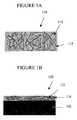
- FIGS. 1A and 1Bare schematic illustrations of matrix-nanotube composites according to the present invention.
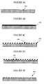
- FIGS. 2 A- 2 Care schematic illustrations of an etching procedure according to the present invention.
- FIGS. 3 A- 3 Dare schematic illustrations of a technique for forming a substrate (e.g.—cathode) with an array of matrix-nanotube composite structures according to the invention.
- FIGS. 4 A- 4 Eare schematic illustrations of an alternative technique of forming a substrate (e.g.—cathode) with an array of fine focal spots for field emission according to the invention.
- a substratee.g.—cathode
- FIGS. 5 A- 5 Care schematic illustrations of an alternative technique of providing a substrate (e.g.—cathode) with fine focal spots for field emission according to the invention.
- a substratee.g.—cathode
- FIGS. 6 A- 6 Eare schematic illustrations of a technique for forming a triode field emission structure according to the present invention.
- a method performed according to the principles of the present inventioncan include a combination of some or all of the following steps: (1) forming a raw nanostructure-containing material by a suitable technique, such as arc-discharge or laser ablation; (2) forming a mixture of nanostructure-containing material and a matrix material; (3) applying the mixture to a supporting surface or substrate, or forming the mixture into a free-standing body; (4) pressing the mixture to improve surface uniformity and/or flatness; (5) sintering or melting the mixture; (6) polishing and rinsing the sintered mixture; (6) etching the sintered mixture to remove matrix material and expose nanostructure material; (7) rinsing the etched mixture; (8) annealing the etched mixture; and (9) aligning the nanostructure material exposed by the etching procedure.
- a suitable techniquesuch as arc-discharge or laser ablation
- the processbegins with pre-formed raw nanostructure-containing material, preferably with a high aspect ratio, or a nanotube-containing material, such as a carbon nanotube-containing material.
- This raw materialcan comprise at least one of single-walled carbon nanotubes, multi-walled carbon nanotubes, silicon, silicon oxide, germanium, germanium oxide, carbon nitrides, boron, boron nitride, dichalcogenide, silver, gold, iron, titanium oxide, gallanium oxide, indium phosphide, or magnetic particles such as Fe, Co, and Ni enclosed within nanostructures.
- the raw carbon nanotube-containing materialcomprises single-walled carbon nanotubes.
- the carbon nanotubescan be formed by any suitable technique, such as the above-mentioned arc-discharge and laser ablation methods.
- These raw materialscan be formed by any suitable technique, such as the above-mentioned arc-discharge technique.
- the raw nanostructure-containing materialcan be subjected to purification.
- a number of techniques for purifying the raw materialsare envisioned.
- the raw materialcan be purified by reflux in a suitable solvent, such as a combination of peroxide (H 2 O 2 ) and water, with an H 2 O 2 concentration of 1-40% by volume, preferably about 20% by volume H 2 O 2 , with subsequent rinsing in CS 2 and then in methanol, followed by filtration.
- a suitable solventsuch as a combination of peroxide (H 2 O 2 ) and water, with an H 2 O 2 concentration of 1-40% by volume, preferably about 20% by volume H 2 O 2 , with subsequent rinsing in CS 2 and then in methanol, followed by filtration.
- H 2 O 2peroxide
- CS 2cycloxide
- methanolmethanol
- the raw nanostructure-containing materialis placed in a suitable liquid medium, such as an acidic medium, an organic solvent, or an alcohol, preferably methanol.
- a suitable liquid mediumsuch as an acidic medium, an organic solvent, or an alcohol, preferably methanol.
- the raw materialsare kept in suspension within the liquid medium for several hours using a high-powered ultrasonic horn, while the suspension is passed through a microporous membrane.
- the raw materialscan be purified by oxidation in air or an oxygen environment at a temperature of 200-700° C. The impurities in the raw materials are oxidized at a faster rate than the nanotubes.
- the raw materialscan be purified by liquid chromatography to separate the nanostructures/nanotubes from the impurities.
- the nanostructures or nanotubescan also be subjected to a shortening process, which shortens the length thereof.
- a shortening processwhich shortens the length thereof.
- carbon nanotubescan be shortened by exposure to a strong acid.
- the nanotubescan be broken or shortened by mechanical milling techniques, such as ball milling.
- the purified raw materialcan also optionally be annealed at a suitable temperature, such as 100° C.-1200° C. According to a preferred embodiment, the annealing temperature is 100° C.-600° C.
- the materialis annealed for a suitable time period, such as approximately 1 to 60 minutes. According to a preferred embodiment, the material is annealed for approximately 1 hour.
- the materialis annealed in a vacuum of about 10 ⁇ 2 torr, or at an even higher vacuum pressure. According to a preferred embodiment, the vacuum is about 5 ⁇ 10 ⁇ 7 torr.
- the matrix materialcan comprise conductive particles that can be electrochemically etched, such as metals, metal alloys, or mixtures thereof. Specific examples include: Fe, Mg, Cu, Co, Ni, Zn, Cr, Al, Au, Ag, Sn, Pb, W and Ti, or mixtures thereof.
- the matrix materialcan comprise metal salts or oxides that decompose at elevated temperatures to render metals that can be electrochemically etched.
- metal salts or oxidesthat decompose at elevated temperatures to render metals that can be electrochemically etched.
- Specific examplesinclude: Fe 2 O 3 , TiO 2 , MgO, and CaO, or mixtures thereof.
- the nanostructure or nanotube material and the matrix materialare combined according to a suitable technique.
- the nanostructure or nanotube materialcan be ground or milled in a suitable solvent such as alcohol or water, to which the matrix material is added and ground or milled together to obtain a uniform mixture thereof in the form of a slurry or suspension.
- a suitable solventsuch as alcohol or water
- the uniformity of the slurry or suspensioncan be improved by the application of ultrasonic energy thereto.
- This suspensioncan be used to form a free-standing body 110 , as illustrated in FIG. 1A, which includes randomly-oriented nanostructures or nanotubes 112 and a matrix 114 .
- the slurry or suspensioncan be dried into a powder-like form, which can then be pressed or otherwise manipulated to form a suitable shape.
- the slurrycan be applied to a supporting surface or a substrate according to suitable technique.
- the substratecan be made of any suitable conductive material, such as metal, metal alloy, graphite, doped silicon.
- the substratecan be formed by a non-conductive material coated with a conductive layer, such as indium-tin oxide glasses, or glass or silicon wafer with deposited metal layer.
- Suitable techniques for application of the slurry or suspensioninclude suspension or solution casting, spraying, spin coating, screen printing, or electrophoretic deposition (EPD).
- a coated body 120is formed and includes randomly-oriented nanostructures or nanotubes 122 embedded within a matrix 124 , thereby forming a coating that is applied to a supporting surface or substrate 126 .
- the proportions of nanostructure or nanotube material and the matrix material present in the mixturecan vary.
- the mixturecan comprise 10% nanotubes and 90% matrix material, by weight.
- the mixtureis deposited onto a supporting surface or substrate by EPD.
- EPDelectrowetting-on-dielectric
- Any suitable EPD processcan be utilized.
- EPD processSee, e.g.—U.S. patent application Ser. No. 60/431,719, now U.S. Pat. No. ______, the content of which is incorporated herein by reference in its entirety.
- such a techniqueincludes formation of a suspension from the mixture, as discussed above.
- concentration of the mixture contained in the suspensioncan vary.
- the suspensioncan contain 0.4 grams of the nanostructure or nanotube/matrix material per 1 ml of liquid media.
- a chargeris added to the suspension in order to facilitate electrophoretic deposition.
- Possible chargersinclude MgCl 2 , Mg(NO 3 ) 2 , La(NO 3 ) 3 , Y(NO 3 ) 3 , AlCl 3 , and sodium hydroxide. Any suitable amount can be utilized. Amounts ranging from less than 1% up to 50%, by weight, as measured relative to the amount of nanostructure or nanotube/matrix material mixture contained in the suspension are feasible. According to a preferred embodiment, the suspension can contain less than 10% of the charger.
- a plurality of electrodesare then introduced into the suspension.
- two electrodesare utilized.
- One of the electrodescomprises the object upon which the mixture is to be deposited. Any suitable object or substrate material is envisioned, so long as it possesses the requisite degree of electrical conductivity.
- the objectis either metal or doped silicon.
- An alternating current, or a direct current,is applied to the electrodes thereby producing an electrical field between the electrodes. This causes the particles of the mixture in the suspension to migrate toward and attach to the substrate electrode.
- the electrophoretic depositioncan be carried out at an elevated temperature or at room temperature. According to a preferred embodiment, the above-described electrophoretic deposition is carried at an elevated temperature. An elevated temperature on the order of 40-60° C. is envisioned.
- the EPDcan occur with application of either a direct current or an alternating current.
- the particular electrodei.e.—anode or the cathode
- the particular electrodei.e.—anode or the cathode
- the particular electrodei.e.—anode or the cathode
- the particular electrodei.e.—anode or the cathode
- the charger materialFor example, the use of a negative charger, such as sodium hydroxide (NaOH) imparts a negative charge to the nanostructure material, thereby creating a tendency for the nanostructure material to migrate towards the positive electrode (cathode).
- a positive charger materialsuch as MgCl 2 , a positive charge is imparted to the nanostructure material, thereby creating a tendency for the nanostructure material to migrate toward the negative electrode (anode).
- the particular electrode to which the nanostructure material migratescan be controlled through the selection of alternating current frequency, dielectric constant of the liquid comparing to the nanostructure material, the field concentration, and the geometry of the electrodes.
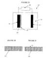
- FIG. 2Aschematically illustrates an arrangement for such an EPD process, the arrangement also being useful for electrochemical etching of the mixture, as will be described later.
- the arrangement 200includes a power supply 210 having positive and negative terminals. The terminals attached to a pair of electrodes 212 and 214 . The electrodes being immersed in a liquid medium 216 .
- the first electrodecomprises the substrate 218 upon which a coating of the mixture 220 is to be deposited.
- the liquid medium 216contains the particles of the mixture, and optionally a charger and/or other additional components.
- the particlesare polarized by the electrical field created between the electrodes in a manner that tends to drive them toward the substrate 212 electrode and attach themselves to the surface thereof.
- the areas of the substrate electrode 212 upon which the mixture is depositedcan be controlled by suitable masking techniques, thereby making the deposition of either uniform or patterned coating possible.
- the process of the present inventionmay optionally include a step whereby the as-deposited coating is pressed against a flat surface, such as a glass or metal plate, thereby improving the smoothness and uniformity of the surface.
- the coating or free-standing bodyis then sintered in order to consolidate the nanostructure or nanotube/matrix composite.
- the sintering stepcan be carried out for example at 300 to 1200 degrees C for up to 3 hours (time) in a vacuum at 5 ⁇ 10 ⁇ 7 torr.
- the sintered bodyWhen in the form of a free-standing body, the sintered body can optionally be sectioned or polished, and rinsed, to provide the body with on or more smooth surfaces.
- the free-standing body or coated substrate formed as described aboveis preferably etched to remove a layer of matrix material from at least a potion of at least one surface of the body or coating.
- the etchingcan be performed according to any suitable technique. However, it is preferred that the etching be achieved by an electrochemical technique. Electrochemical etching is preferred over other techniques such as acid etching, etc., because: (i) the etch rate can be easily controlled by controlling the electrical current generated by the power source, the etch time; (ii) electrochemical etching allows for greater selectivity with respect to the material being etched, and the material which should not be etched; and (iii) the electrochemical etching step can be easily integrated into a process that also includes EPD, since the basic equipment set-up is the same for both steps. In fact, according to the present invention a process incorporating both EPD and electrochemical etching imparts a certain synergy to the process, enabling superior control, convenience, and gains in efficiency, when compared to existing techniques.
- the coated substrateforms a cathode 212 of the power supply 210 .
- Another conducting plate 214preferably stainless steel or carbon electrode is connected to the negative electrode of the power supply 210 .
- the two electrodes 212 , 214are immersed in an electrochemical bath 216 .
- the liquid medium or bath 216can be an aqueous, or a non-aqueous solution of acids, bases or the salts containing the elements of the materials to be etched, i.e.—of the matrix material.
- any bath that is used to electrochemically plate a metal or metal alloycan be used to electrochemically etch a metal or alloy.
- the coating 220comprises a Fe/carbon nanotube composite
- the electrochemical bath 216 used for plating Fecan be used to etch a Fe layer away from the Fe/carbon nanotube composite coating 220 .
- the Fe atoms in the Fe/carbon nanotube compositeget oxidized and dissolved into the plating bath 216 at the positive electrode 212 and the same number of Fe atoms will be deposited at the negative electrode 214 to attain electrical neutrality.
- the carbon materialsare very stable during electrochemical reaction so that they typically will survive the etching process.
- the etching stepcan be performed at room temperature or at an elevated temperature. According to a preferred embodiment, the electrochemical etching step is performed at an elevated temperature on the order of 30-90° C.
- the etching bathcould be aqueous solution of ferrous sulfate (FeSO 4 ) at concentration of 240 g/L.
- FeSO 4ferrous sulfate
- the pH value of the bathis between 2.8-3.5 and the temperature of the bath is between 32-66° C.
- the current densityis preferably between 20-40 A/ft 2 and the voltage is between 1-20V.
- FIGS. 2B and 2Cschematically illustrate a coated substrate before etching 220 ′, and a coated substrate after etching 220 ′′, respectively.
- the etching stepexposes a number of nanostructures or nanotubes 221 at the desired emission surface of the coated substrate.
- the structure(s)are optionally rinsed thoroughly using de-ionized water and alcohol. They are then optionally annealed under a dynamic vacuum to get rid of the moisture and solvents introduced into the structures during processing.
- Suitable exemplary annealing conditionscomprise 850° C. at 5 ⁇ 10 ⁇ 7 for 1.5 hours.
- the coated substrate or free-standing bodycan be further processed in a manner which promotes alignment of the nanostructures or nanotubes in the direction of electron emission. Numerous techniques are feasible. According to an exemplary embodiment, the coated substrate or free-standing body can be subjected to a high frequency voltage pulse.
- the voltage of the pulseis from a few volts to several thousand volts depending on the distance between the cathode and the anode.
- the frequencyis from a few KHz to the MHz range. Preferably, a few MHz.
- the time of the processescan be up to a few hours but preferably just a few minutes.
- the alignment stepcan be performed at any suitable time in the process, preferably after exposure of the nanostructures or nanotubes by etching, and prior to powering up the coated substrate or free-standing body for electron emission.
- Field emission cathodes with an fine pixel size or matrix of emission pixelscan also be made by the above method.
- a metal/carbon nanotube paste 320can be deposited on a waffled substrate 310 by a doctor-blade or similar device, spin coating, screen-printing or electrophoresis.
- the coated pasteis sintered or melted under proper conditions thereby rendering small deposits of nanotube-metal composite 330 .
- the top surface 340 of the coated substrateis polished and rinsed thoroughly using alcohol.
- the metal/carbon nanotube compositeis limited to cavities 312 .
- the structuresare then etched and rinsed, preferably by the above-described electrochemical technique, so that these areas have exposed carbon nanotube emitters 350 (FIG. 3D).
- the exposed nanotubesmay also be subjected to an alignment treatment, as discussed above.
- FIGS. 4 A- 4 ESimilar structures can also be made by photolithography techniques, as shown in FIGS. 4 A- 4 E.
- a photoresist layer 420is deposited on the metal/carbon nanotube composite pellet or film 410 .
- a patterned structure 430is formed having open areas 440 .
- the pellet or film 410is electrochemically etched, at these areas exposed to the bath by openings 440 . Consequently, carbon nanotube emitters 450 are left exposed.
- the exposed nanotubes 450may also be subjected to an alignment treatment, as previously discussed.
- the photoresistor layer 430is stripped away and a patterned cathode 460 is formed. Because photolithography techniques can pattern very small features, a cathode with extremely fine focal spots, as shown in FIG. 4E, can be made easily by the above-described process.
- Field emission cathodes with a fine focal spot or arrays of fine focal spotscan also be made by a process such as the one shown in FIGS. 5 A- 5 C.
- a substratecomprises a disk 510 with a hole 512 , and a cone 514 with a hole 516 .
- a metal/carbon nanotube paste 520is filled into the hole 516 according to the above-described techniques, as shown in FIG. 5B.
- the filled hole(s)are vacuum annealed at high temperature thereby forming deposits of nanotube-metal composite 530 .
- the surface(s) of the composite 530are then etched electrochemically to make sure that significant number of carbon nanotubes 540 are exposed from the metal matrix as shown in FIG. 5C.
- the exposed nanotubesare subjected to the previously described alignment process step.
- the front surfaces 550are polished and further cleaned so that the emitting materials only exist in the holes.
- the metal/carbon nanotubes pastecan also be filled into the structures from the back as shown by the large arrow in FIG. 5A.
- the front surfaces 550 and the side surfaces 560can be covered before filling by using Para-film or other films. They can be peeled off after the filling process so that the front (emitting) surface will only have emitting materials in the hole 516 areas.
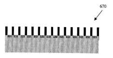
- a triode field emission structurecan also be made by photolithography techniques, as shown in FIGS. 6 A- 6 E.
- a dielectric layer 620is deposited onto a carbon nanotube/metal composite film or body 610 .
- a conducting layer 630is deposited on the dielectric layer 620 .
- a photoresister layer 640is deposited on the conducting layer 630 and is exposed and developed.
- a patterned structure with openings 650 as shown in FIGS. 6 B- 6 Ecan be made by normal photolithography techniques.
- a layer of the nanotube/metal composite 610can be etched away by electrochemical etching thereby exposing the nanotube emitters 660 at the surface thereof (FIG. 6D).
- the exposed nanotubes 660can optionally be subjected to an alignment step.
- the remaining photoresist layeris stripped away.
- the resulting triode field emission cathode 670is shown in FIG. 6E.
Landscapes
- Chemical & Material Sciences (AREA)
- Engineering & Computer Science (AREA)
- Materials Engineering (AREA)
- Nanotechnology (AREA)
- Chemical Kinetics & Catalysis (AREA)
- Electrochemistry (AREA)
- Metallurgy (AREA)
- Organic Chemistry (AREA)
- Theoretical Computer Science (AREA)
- Mathematical Physics (AREA)
- Crystallography & Structural Chemistry (AREA)
- Physics & Mathematics (AREA)
- Manufacturing & Machinery (AREA)
- Cold Cathode And The Manufacture (AREA)
- Carbon And Carbon Compounds (AREA)
Abstract
Description
- This application claims priority under 35 U.S.C. 119 to U.S. Provisional Application No. 60/393,097 entitled “Fabrication and Activation Processes of Field Emission Cathodes Composed of Carbon Nanotubes/Metal Composites”, and filed on Jul. 3, 2002, the entire content of which is incorporated herein by reference[0001]
- The present invention is directed to improved techniques for the formation field emission structures and devices that incorporate nanostructure-containing material, as well as treatments to improve the performance thereof. The present invention is also directed to associated structures and devices.[0002]
- Various constructions and techniques will be described below. However, nothing described herein should be construed as an admission of prior art. To the contrary, Applicants expressly reserve the right to demonstrate, where appropriate, that anything described herein does not qualify as prior art under the applicable statutory provisions.[0003]
- The term “nanostructure” material is used by those familiar with the art to designate materials including nanoparticles such as C[0004]60fullerenes, fullerene-type concentric graphitic particles, metal, compound semiconductors such as CdSe, InP; nanowires/nanorods such as Si, Ge, SiOx, GeOx, or nanotubes composed of either single or multiple elements such as carbon, BxNy, CxByNz, MoS2, and WS2. One of the common features of nanostructure materials is their basic building blocks. A single nanoparticle or a carbon nanotube has a dimension that is less than 500 nm at least in one direction. These types of materials have been shown to exhibit certain properties that have raised interest in a variety of applications and processes.
- Nanostructures, such as carbon nanotubes, are known to be excellent electron field emitters due to their unique geometry, extremely high mechanical strength, and good chemical and thermal stability. Experiments have shown that they have a low threshold field for electron emission (˜1-2V/μm) and are capable of emitting at very high current densities.[0005]
- However, due to materials issues such as poor film uniformity and insufficient adhesion and electrical conductivity between carbon nanotubes and the substrate, high stable emission current has not been obtained from macroscopic carbon nanotube-containing structures and devices, which has limited their practical utilization.[0006]
- Among all the available techniques for synthesizing carbon nanotubes, laser-ablation and arc-discharge methods produce carbon nanotubes with a high level of structural perfection and therefore amongst the best electron field-emission properties. However, materials made therefrom are in the form of either porous membranes or powders that are not easily incorporated into field-emission devices such as cathodes cannot be used directly on devices without further processing. Although the chemical vapor deposition (CVD) methods can grow carbon nanotubes directly on substrates, they require very high temperatures (600-1000° C.) and a reactive environment. Also, CVD grown carbon nanotubes generally do not have the same level of structural perfection and, as a result, lack the same emission properties as the tubes made by laser-ablation or arc-discharge methods. To fully utilize the excellent electron field-emission properties of carbon nanotubes, especially single wall carbon nanotubes made by laser-ablation and arc-discharge methods, some deposition techniques have been developed.[0007]
- In addition, the nanotubes contained in powders or soot formed by laser-ablation and arc-discharge methods are randomly oriented. However, when utilized as sources for electron emission, it is advantageous to orient the tips of the nanotubes in the same direction, such as toward a common emission target. Thus, the normal lack of orientation of the nanotubes presents and additional challenge to their utilization in field-emission devices.[0008]
- Representative disclosures of nanostructure containing materials, devices and techniques include the following.[0009]
- U.S. Pat. No. ______ (Ser. No. 09/296,572 entitled “Device Comprising Carbon Nanotube Field Emitter Structure and Process for Forming Device”), the disclosure of which is incorporated herein by reference, in its entirety, discloses a carbon nanotube-based electron emitter structure.[0010]
- U.S. Pat. No. ______ (Ser. No. 09/351,537 entitled “Device Comprising Thin Film Carbon Nanotube Electron Field Emitter Structure”), the disclosure of which is incorporated herein by reference, in its entirety, discloses a carbon nanotube field emitter structure having a high emitted current density.[0011]
- U.S. Pat. No. 6,553,096 entitled “X-Ray Generating Mechanism Using Electron Field-Emission Cathode”, the disclosure of which is incorporated herein by reference, in its entirety, discloses an x-ray generating device incorporating a cathode formed at least in part with a nanostructure-containing material.[0012]
- U.S. Patent Application Publication No. US-2002/0094064, entitled “Large-Area Individually Addressable Multi-Beam X-Ray System and Method of Forming Same”, the disclosure of which is incorporated herein by reference, in its entirety, discloses structures and techniques for generating x-rays which includes a plurality of stationary and individually electrically addressable field emissive electron sources.[0013]
- U.S. Pat. No. ______ (Ser. No. 10/358,160 entitled “Method and Apparatus for Controlling Electron Beam Current”), the disclosure of which is incorporated herein by reference, in its entirety, discloses an x-ray generating device which allows independent control of the electron emission current by piezoelectric, thermal, or optical means.[0014]
- U.S. Patent Application Publication No. US-2002/0140336, entitled “Coated Electrode with Enhanced Electron Emission and Ignition Characteristics”, the disclosure of which is incorporated herein by reference, in its entirety, discloses a coated electrode construction which incorporates nanostructure-containing materials.[0015]
- U.S. Pat. No. ______ (application Ser. No. 10/448,144), entitled “Nanomaterial Based Electron Field-Emission Cathodes for Vacuum and Gaseous Electronics”), the disclosure of which is incorporated herein by reference, in its entirety, discloses electronics incorporating field-emission cathodes based at least in part on nanostructure-containing materials.[0016]
- U.S. Pat. No. 6,385,292 entitled “Solid State CT System and Method”, the disclosure of which is incorporated herein by reference, in its entirety, disclose an x-ray source including a cathode formed from a plurality of addressable elements.[0017]
- U.S. Pat. No. ______, (application Ser. No. 10/464,440), filed Jun. 19, 2003) entitled “Improved Electrode and Associated Devices and Methods”, the disclosure of which is incorporated herein by reference, in its entirety, discloses a device including cathode incorporating a nanostructure-containing material embedded in a matrix material.[0018]
- Therefore, processes which can readily incorporate carbon nanotubes, or other nanostructure-containing materials, formed by arc-discharge, laser ablation techniques, and the like, into adherent robust field emission devices while provide good electrical conductivity and a substantial number of nanotubes protruding toward the emission direction are desired.[0019]
- The present invention provides fabrication and activation methods for a field emission devices, such as cathodes, which comprise a nanostructure-containing material composite. Nanostructure-containing materials are mixed with particles of other materials, such as (1) conducting materials including metal or metal alloys or (2) non-conducting materials including metal oxides or salts. The mixture is either (1) coated on the surface of a supporting structure or, (2) pressed, sintered or melted into a compact free-standing body. The coating can be either uniform or patterned with a predetermined structure. The free-standing body is processed to the desired geometry.[0020]
- The coating or free-standing body may be the further processed to improve electron emission characteristics. One such method to improve the electron field emission properties is by electrochemical etching of the surface. A high frequency pulse can be used to further align the carbon nanotubes protruding from the composite surface.[0021]
- Compared with thin carbon nanotube films, a coating formed as described above provides better adhesion and electrical conductivity between the nanostructure-containing material and the substrate.[0022]
- According the one aspect, the present invention provides a method of forming an electron emitter that includes the steps of: (i) forming a nanostructure-containing material; (ii) forming a mixture of nanostructure-containing material and a matrix material; (iii) depositing a layer of the mixture onto at least a portion of at least one surface of a substrate by electrophoretic deposition; (iv) sintering or melting the layer thereby forming a composite; and (v) electrochemically etching the composite to remove matrix material from a surface thereof, thereby exposing nanostructure-containing material.[0023]
- FIGS. 1A and 1B are schematic illustrations of matrix-nanotube composites according to the present invention.[0024]
- FIGS.[0025]2A-2C are schematic illustrations of an etching procedure according to the present invention.
- FIGS.[0026]3A-3D are schematic illustrations of a technique for forming a substrate (e.g.—cathode) with an array of matrix-nanotube composite structures according to the invention.
- FIGS.[0027]4A-4E are schematic illustrations of an alternative technique of forming a substrate (e.g.—cathode) with an array of fine focal spots for field emission according to the invention.
- FIGS.[0028]5A-5C are schematic illustrations of an alternative technique of providing a substrate (e.g.—cathode) with fine focal spots for field emission according to the invention.
- FIGS.[0029]6A-6E are schematic illustrations of a technique for forming a triode field emission structure according to the present invention.
- Exemplary arrangements and techniques according to the present invention will now be described by reference to the drawing figures.[0030]
- Generally, a method performed according to the principles of the present invention can include a combination of some or all of the following steps: (1) forming a raw nanostructure-containing material by a suitable technique, such as arc-discharge or laser ablation; (2) forming a mixture of nanostructure-containing material and a matrix material; (3) applying the mixture to a supporting surface or substrate, or forming the mixture into a free-standing body; (4) pressing the mixture to improve surface uniformity and/or flatness; (5) sintering or melting the mixture; (6) polishing and rinsing the sintered mixture; (6) etching the sintered mixture to remove matrix material and expose nanostructure material; (7) rinsing the etched mixture; (8) annealing the etched mixture; and (9) aligning the nanostructure material exposed by the etching procedure.[0031]
- The process begins with pre-formed raw nanostructure-containing material, preferably with a high aspect ratio, or a nanotube-containing material, such as a carbon nanotube-containing material. This raw material can comprise at least one of single-walled carbon nanotubes, multi-walled carbon nanotubes, silicon, silicon oxide, germanium, germanium oxide, carbon nitrides, boron, boron nitride, dichalcogenide, silver, gold, iron, titanium oxide, gallanium oxide, indium phosphide, or magnetic particles such as Fe, Co, and Ni enclosed within nanostructures. According to a preferred embodiment, the raw carbon nanotube-containing material comprises single-walled carbon nanotubes. The carbon nanotubes can be formed by any suitable technique, such as the above-mentioned arc-discharge and laser ablation methods.[0032]
- It is also contemplated by the present invention that raw materials be in the form of nanotube structures with a composition of B[0033]xCyNz(B=boron, C=carbon, and N=nitrogen), or nanotube or concentric fullerene structures with a composition MS2(M=tungsten, molybdenum, or vanadium oxide) can be utilized. These raw materials can be formed by any suitable technique, such as the above-mentioned arc-discharge technique.
- The raw nanostructure-containing material can be subjected to purification. A number of techniques for purifying the raw materials are envisioned. For example, the raw material can be purified by reflux in a suitable solvent, such as a combination of peroxide (H[0034]2O2) and water, with an H2O2concentration of 1-40% by volume, preferably about 20% by volume H2O2, with subsequent rinsing in CS2and then in methanol, followed by filtration. According to an exemplary technique, approximately 10-100 ml of peroxide is introduced into the medium for every 1-10 mg of nanotubes in the medium, and the reflux reaction is carried out at a temperature of 20-100° C. (see, e.g.—U.S. Pat. No. ______ (Ser. No. 09/679,303)).
- According to another alternative, the raw nanostructure-containing material is placed in a suitable liquid medium, such as an acidic medium, an organic solvent, or an alcohol, preferably methanol. The raw materials are kept in suspension within the liquid medium for several hours using a high-powered ultrasonic horn, while the suspension is passed through a microporous membrane. In another embodiment, the raw materials can be purified by oxidation in air or an oxygen environment at a temperature of 200-700° C. The impurities in the raw materials are oxidized at a faster rate than the nanotubes.[0035]
- In yet another embodiment, the raw materials can be purified by liquid chromatography to separate the nanostructures/nanotubes from the impurities.[0036]
- The nanostructures or nanotubes can also be subjected to a shortening process, which shortens the length thereof. For example, carbon nanotubes can be shortened by exposure to a strong acid. Alternatively, the nanotubes can be broken or shortened by mechanical milling techniques, such as ball milling.[0037]
- The purified raw material, regardless of whether subjected to the above-described shortening process, can also optionally be annealed at a suitable temperature, such as 100° C.-1200° C. According to a preferred embodiment, the annealing temperature is 100° C.-600° C. The material is annealed for a suitable time period, such as approximately 1 to 60 minutes. According to a preferred embodiment, the material is annealed for approximately 1 hour. The material is annealed in a vacuum of about 10[0038]−2torr, or at an even higher vacuum pressure. According to a preferred embodiment, the vacuum is about 5×10⁻⁷torr.
- Next the nanostructure or nanotube materials are combined with a matrix material to form a mixture thereof. The matrix material can comprise conductive particles that can be electrochemically etched, such as metals, metal alloys, or mixtures thereof. Specific examples include: Fe, Mg, Cu, Co, Ni, Zn, Cr, Al, Au, Ag, Sn, Pb, W and Ti, or mixtures thereof.[0039]
- Alternatively, the matrix material can comprise metal salts or oxides that decompose at elevated temperatures to render metals that can be electrochemically etched. Specific examples include: Fe[0040]2O3, TiO2, MgO, and CaO, or mixtures thereof.
- The nanostructure or nanotube material and the matrix material are combined according to a suitable technique. For example, the nanostructure or nanotube material can be ground or milled in a suitable solvent such as alcohol or water, to which the matrix material is added and ground or milled together to obtain a uniform mixture thereof in the form of a slurry or suspension. The uniformity of the slurry or suspension can be improved by the application of ultrasonic energy thereto.[0041]
- This suspension can be used to form a free-standing[0042]
body 110, as illustrated in FIG. 1A, which includes randomly-oriented nanostructures ornanotubes 112 and amatrix 114. Optionally, the slurry or suspension can be dried into a powder-like form, which can then be pressed or otherwise manipulated to form a suitable shape. - Alternatively, the slurry can be applied to a supporting surface or a substrate according to suitable technique. The substrate can be made of any suitable conductive material, such as metal, metal alloy, graphite, doped silicon. Alternatively, the substrate can be formed by a non-conductive material coated with a conductive layer, such as indium-tin oxide glasses, or glass or silicon wafer with deposited metal layer.[0043]
- Suitable techniques for application of the slurry or suspension include suspension or solution casting, spraying, spin coating, screen printing, or electrophoretic deposition (EPD). As illustrated in FIG. 1B, a[0044]
coated body 120 is formed and includes randomly-oriented nanostructures ornanotubes 122 embedded within amatrix 124, thereby forming a coating that is applied to a supporting surface orsubstrate 126. - The proportions of nanostructure or nanotube material and the matrix material present in the mixture can vary. According to one exemplary embodiment, the mixture can comprise 10% nanotubes and 90% matrix material, by weight.[0045]
- According to a preferred embodiment, the mixture is deposited onto a supporting surface or substrate by EPD. Any suitable EPD process can be utilized. For specific details of exemplary techniques, see, e.g.—U.S. patent application Ser. No. 60/431,719, now U.S. Pat. No. ______, the content of which is incorporated herein by reference in its entirety.[0046]
- Generally, such a technique includes formation of a suspension from the mixture, as discussed above. The concentration of the mixture contained in the suspension can vary. For example, the suspension can contain 0.4 grams of the nanostructure or nanotube/matrix material per 1 ml of liquid media.[0047]
- Optionally, a charger is added to the suspension in order to facilitate electrophoretic deposition. Possible chargers include MgCl[0048]2, Mg(NO3)2, La(NO3)3, Y(NO3)3, AlCl3, and sodium hydroxide. Any suitable amount can be utilized. Amounts ranging from less than 1% up to 50%, by weight, as measured relative to the amount of nanostructure or nanotube/matrix material mixture contained in the suspension are feasible. According to a preferred embodiment, the suspension can contain less than 10% of the charger.
- A plurality of electrodes are then introduced into the suspension. According to a preferred embodiment, two electrodes are utilized. One of the electrodes comprises the object upon which the mixture is to be deposited. Any suitable object or substrate material is envisioned, so long as it possesses the requisite degree of electrical conductivity. According to a preferred embodiment, the object is either metal or doped silicon.[0049]
- An alternating current, or a direct current, is applied to the electrodes thereby producing an electrical field between the electrodes. This causes the particles of the mixture in the suspension to migrate toward and attach to the substrate electrode.[0050]
- The electrophoretic deposition can be carried out at an elevated temperature or at room temperature. According to a preferred embodiment, the above-described electrophoretic deposition is carried at an elevated temperature. An elevated temperature on the order of 40-60° C. is envisioned.[0051]
- The EPD can occur with application of either a direct current or an alternating current. For instance, when direct current is applied, the particular electrode (i.e.—anode or the cathode) to which the nanostructure material migrates can be controlled through the selection of the charger material. For example, the use of a negative charger, such as sodium hydroxide (NaOH) imparts a negative charge to the nanostructure material, thereby creating a tendency for the nanostructure material to migrate towards the positive electrode (cathode). Conversely, when a positive charger material is used, such as MgCl[0052]2, a positive charge is imparted to the nanostructure material, thereby creating a tendency for the nanostructure material to migrate toward the negative electrode (anode).
- When an alternating current field is used, the particular electrode to which the nanostructure material migrates can be controlled through the selection of alternating current frequency, dielectric constant of the liquid comparing to the nanostructure material, the field concentration, and the geometry of the electrodes.[0053]
- FIG. 2A schematically illustrates an arrangement for such an EPD process, the arrangement also being useful for electrochemical etching of the mixture, as will be described later. Generally, as illustrated in FIG. 2A, the[0054]
arrangement 200 includes apower supply 210 having positive and negative terminals. The terminals attached to a pair ofelectrodes liquid medium 216. For the EPD process, the first electrode comprises thesubstrate 218 upon which a coating of themixture 220 is to be deposited. Theliquid medium 216 contains the particles of the mixture, and optionally a charger and/or other additional components. The particles are polarized by the electrical field created between the electrodes in a manner that tends to drive them toward thesubstrate 212 electrode and attach themselves to the surface thereof. The areas of thesubstrate electrode 212 upon which the mixture is deposited can be controlled by suitable masking techniques, thereby making the deposition of either uniform or patterned coating possible. - When a coating is formed by an EPD technique, the process of the present invention may optionally include a step whereby the as-deposited coating is pressed against a flat surface, such as a glass or metal plate, thereby improving the smoothness and uniformity of the surface.[0055]
- The coating or free-standing body is then sintered in order to consolidate the nanostructure or nanotube/matrix composite. The sintering step can be carried out for example at 300 to 1200 degrees C for up to 3 hours (time) in a vacuum at 5×10[0056]−7torr.
- When in the form of a free-standing body, the sintered body can optionally be sectioned or polished, and rinsed, to provide the body with on or more smooth surfaces.[0057]
- Next the free-standing body or coated substrate formed as described above is preferably etched to remove a layer of matrix material from at least a potion of at least one surface of the body or coating.[0058]
- The etching can be performed according to any suitable technique. However, it is preferred that the etching be achieved by an electrochemical technique. Electrochemical etching is preferred over other techniques such as acid etching, etc., because: (i) the etch rate can be easily controlled by controlling the electrical current generated by the power source, the etch time; (ii) electrochemical etching allows for greater selectivity with respect to the material being etched, and the material which should not be etched; and (iii) the electrochemical etching step can be easily integrated into a process that also includes EPD, since the basic equipment set-up is the same for both steps. In fact, according to the present invention a process incorporating both EPD and electrochemical etching imparts a certain synergy to the process, enabling superior control, convenience, and gains in efficiency, when compared to existing techniques.[0059]
- The basic idea of electrochemical etching used in this invention is similar to that used in electrochemical plating. As shown in FIG. 2, the coated substrate forms a[0060]
cathode 212 of thepower supply 210. Another conductingplate 214, preferably stainless steel or carbon electrode is connected to the negative electrode of thepower supply 210. The twoelectrodes electrochemical bath 216. - The liquid medium or[0061]
bath 216 can be an aqueous, or a non-aqueous solution of acids, bases or the salts containing the elements of the materials to be etched, i.e.—of the matrix material. In principle, any bath that is used to electrochemically plate a metal or metal alloy can be used to electrochemically etch a metal or alloy. For example, if thecoating 220 comprises a Fe/carbon nanotube composite, theelectrochemical bath 216 used for plating Fe can be used to etch a Fe layer away from the Fe/carbonnanotube composite coating 220. During electrochemical etching, the Fe atoms in the Fe/carbon nanotube composite get oxidized and dissolved into theplating bath 216 at thepositive electrode 212 and the same number of Fe atoms will be deposited at thenegative electrode 214 to attain electrical neutrality. The carbon materials are very stable during electrochemical reaction so that they typically will survive the etching process. - The etching step can be performed at room temperature or at an elevated temperature. According to a preferred embodiment, the electrochemical etching step is performed at an elevated temperature on the order of 30-90° C.[0062]
- As an example, if the matrix material is Fe, the etching bath could be aqueous solution of ferrous sulfate (FeSO[0063]4) at concentration of 240 g/L. Preferably, the pH value of the bath is between 2.8-3.5 and the temperature of the bath is between 32-66° C. The current density is preferably between 20-40 A/ft2and the voltage is between 1-20V.
- FIGS. 2B and 2C schematically illustrate a coated substrate before etching[0064]220′, and a coated substrate after etching220″, respectively. As illustrated in FIG. 2C, the etching step exposes a number of nanostructures or
nanotubes 221 at the desired emission surface of the coated substrate. - After electrochemical etching, the structure(s) are optionally rinsed thoroughly using de-ionized water and alcohol. They are then optionally annealed under a dynamic vacuum to get rid of the moisture and solvents introduced into the structures during processing. Suitable exemplary annealing conditions comprise 850° C. at 5×10[0065]−7for 1.5 hours.
- The coated substrate or free-standing body can be further processed in a manner which promotes alignment of the nanostructures or nanotubes in the direction of electron emission. Numerous techniques are feasible. According to an exemplary embodiment, the coated substrate or free-standing body can be subjected to a high frequency voltage pulse. The voltage of the pulse is from a few volts to several thousand volts depending on the distance between the cathode and the anode. The frequency is from a few KHz to the MHz range. Preferably, a few MHz. The time of the processes can be up to a few hours but preferably just a few minutes. The alignment step can be performed at any suitable time in the process, preferably after exposure of the nanostructures or nanotubes by etching, and prior to powering up the coated substrate or free-standing body for electron emission.[0066]
- Numerous modifications and extrapolations are possible within the basic framework of a method performed as described above. Exemplary, non-limiting, additional methods performed according to the principles of the present invention outlined above will now be described.[0067]
- Field emission cathodes with an fine pixel size or matrix of emission pixels can also be made by the above method. As shown in FIGS.[0068]3A-3D, a metal/
carbon nanotube paste 320 can be deposited on a waffledsubstrate 310 by a doctor-blade or similar device, spin coating, screen-printing or electrophoresis. The coated paste is sintered or melted under proper conditions thereby rendering small deposits of nanotube-metal composite 330. Thetop surface 340 of the coated substrate is polished and rinsed thoroughly using alcohol. As shown in FIG. 3C, the metal/carbon nanotube composite is limited to cavities312. The structures are then etched and rinsed, preferably by the above-described electrochemical technique, so that these areas have exposed carbon nanotube emitters350 (FIG. 3D). The exposed nanotubes may also be subjected to an alignment treatment, as discussed above. - Similar structures can also be made by photolithography techniques, as shown in FIGS.[0069]4A-4E. A
photoresist layer 420 is deposited on the metal/carbon nanotube composite pellet orfilm 410. After developing, apatterned structure 430 is formed havingopen areas 440. The pellet orfilm 410 is electrochemically etched, at these areas exposed to the bath byopenings 440. Consequently,carbon nanotube emitters 450 are left exposed. The exposednanotubes 450 may also be subjected to an alignment treatment, as previously discussed. Thephotoresistor layer 430 is stripped away and a patternedcathode 460 is formed. Because photolithography techniques can pattern very small features, a cathode with extremely fine focal spots, as shown in FIG. 4E, can be made easily by the above-described process. - Field emission cathodes with a fine focal spot or arrays of fine focal spots can also be made by a process such as the one shown in FIGS.[0070]5A-5C. A substrate comprises a
disk 510 with ahole 512, and acone 514 with ahole 516. A metal/carbon nanotube paste 520 is filled into thehole 516 according to the above-described techniques, as shown in FIG. 5B. Preferably, the filled hole(s) are vacuum annealed at high temperature thereby forming deposits of nanotube-metal composite 530. The surface(s) of the composite530 are then etched electrochemically to make sure that significant number ofcarbon nanotubes 540 are exposed from the metal matrix as shown in FIG. 5C. Optionally, the exposed nanotubes are subjected to the previously described alignment process step. If necessary, the front surfaces550 are polished and further cleaned so that the emitting materials only exist in the holes. The metal/carbon nanotubes paste can also be filled into the structures from the back as shown by the large arrow in FIG. 5A. The front surfaces550 and the side surfaces560 can be covered before filling by using Para-film or other films. They can be peeled off after the filling process so that the front (emitting) surface will only have emitting materials in thehole 516 areas. - A triode field emission structure can also be made by photolithography techniques, as shown in FIGS.[0071]6A-6E. A
dielectric layer 620 is deposited onto a carbon nanotube/metal composite film orbody 610. Aconducting layer 630 is deposited on thedielectric layer 620. Aphotoresister layer 640 is deposited on theconducting layer 630 and is exposed and developed. A patterned structure withopenings 650 as shown in FIGS.6B-6E can be made by normal photolithography techniques. A layer of the nanotube/metal composite 610 can be etched away by electrochemical etching thereby exposing thenanotube emitters 660 at the surface thereof (FIG. 6D). The exposednanotubes 660 can optionally be subjected to an alignment step. The remaining photoresist layer is stripped away. The resulting triodefield emission cathode 670 is shown in FIG. 6E. - The above-described techniques can be used to form electron emitters for use in a number of different devices such as flat-panel displays, microwave vacuum tubes, portable x-ray devices, gas discharge tubes, etc.[0072]
- While the present invention has been described by reference to the above-mentioned embodiments, certain modifications and variations will be evident to those of ordinary skill in the art. Therefore, the present invention is limited only by the scope and spirit of the appended claims.[0073]
Claims (25)
1. A method of forming an electron emitter, the method comprising the steps of:
(i) forming a nanostructure-containing material;
(ii) forming a mixture comprising nanostructure-containing material and a matrix material;
(iii) depositing a layer of the mixture onto at least a portion of at least one surface of a substrate by electrophoretic deposition;
(iv) sintering or melting the layer thereby forming a composite; and
(v) electrochemically etching the composite to remove matrix material from a surface thereof, thereby exposing nanostructure-containing material.
2. The method ofclaim 1 , further comprising the step of:
pressing the layer after step (iii), thereby improving surface smoothness of the layer.
3. The method ofclaim 2 , further comprising the step of:
polishing and rinsing a surface of the composite subsequent to step (iv).
4. The method ofclaim 3 , further comprising the step of:
rinsing the composite subsequent to step (v).
5. The method ofclaim 4 , further comprising the step of:
annealing the composite subsequent to step (v).
6. The method ofclaim 5 , further comprising the step of:
aligning at least a portion of the expose nanostructure material.
7. The method ofclaim 1 , wherein step (i) comprises forming the nanostructure-containing material by laser-ablation or arc-discharge techniques, and the nanostructure-containing material comprises single-walled carbon nanotubes.
8. The method ofclaim 1 , further comprising the step of purifying the nanostructure-containing material prior to step (ii).
9. The method ofclaim 1 , wherein the nanostructure-containing material comprises nanotubes, and the method further comprises the step of shortening the length of the nanotubes prior the step (ii).
10. The method ofclaim 9 , wherein the nanotubes are shortened by exposure to an acid or by milling.
11. The method ofclaim 1 , wherein the matrix material comprises: Fe, Mg, Cu, Co, Ni, Zn, Cr, Al, Au, Ag, Sn, Pb, W, Ti, or mixtures thereof.
12. The method ofclaim 1 , wherein the matrix material added at step (ii) comprises: Fe2O3, TiO2, MgO, CaO; or mixtures thereof.
13. The method ofclaim 1 , wherein step (ii) comprises milling the nanostructure-containing material and matrix material, thereby forming a uniform mixture.
14. The method ofclaim 1 , wherein step (ii) comprises forming a suspension of nanostructure-containing material and matrix material.
15. The method ofclaim 1 , wherein the substrate comprises: metal, metal alloy, doped silicon, graphite, or a non-conductive material coated with a layer of indium-tin-oxide glass or metal.
16. The method ofclaim 1 , wherein step (iii) further comprises forming a suspension of the mixture, adding a charger to the suspension, introducing the substrate and a counter electrode into the suspension, connecting the substrate and counter electrode to a power source, and applying current to the substrate and counter electrode thereby causing polarization of the mixture in a matter that causes the mixture to migrate toward and attach to an exposed surface of the substrate.
17. The method ofclaim 16 , wherein step (iii) further comprising masking at least a portion of the substrate thereby shielding the portion from the suspension.
18. The method ofclaim 1 , wherein step (iii) is performed at a temperature of 20-50° C.
19. The method ofclaim 1 , wherein step (iv) is performed at a temperature of 300-1200° C.
20. The method ofclaim 1 , wherein the at least one surface of the substrate comprises a waffled surface with a plurality of cavities.
21. The method ofclaim 1 further comprising the steps of:
applying a photoresist layer to the at least one surface of the substrate and developing the photoresist layer in a manner which forms a pattern of openings therein, prior to step (iii), whereby the openings expose selected portions of the at least one surface of the substrate to the mixture in step (iii).
22. The method ofclaim 21 , further comprising the step of:
removing the photoresist material from the at least one surface of the substrate subsequent to step (iii).
23. The method ofclaim 1 , wherein the substrate comprises a disk and a cone, each with a hole formed therein for receipt of the mixture.
24. The method ofclaim 1 , further comprising, prior to step (iii), the steps of:
depositing a dielectric layer on the at least one surface of the substrate;
depositing a conducting layer on the dielectric layer;
depositing a photoresist layer on the conducting layer;
developing the photoresist layer in a manner which forms a pattern of openings therein; and
removing the portions of the dielectric layer and conducting layer exposed by the pattern of openings.
25. The method ofclaim 24 , further comprising the step of:
removing the photoresist material subsequent to step (iii).
Priority Applications (1)
| Application Number | Priority Date | Filing Date | Title |
|---|---|---|---|
| US10/610,591US7294248B2 (en) | 2002-07-03 | 2003-07-02 | Fabrication and activation processes for nanostructure composite field emission cathodes |
Applications Claiming Priority (2)
| Application Number | Priority Date | Filing Date | Title |
|---|---|---|---|
| US39309702P | 2002-07-03 | 2002-07-03 | |
| US10/610,591US7294248B2 (en) | 2002-07-03 | 2003-07-02 | Fabrication and activation processes for nanostructure composite field emission cathodes |
Publications (2)
| Publication Number | Publication Date |
|---|---|
| US20040108298A1true US20040108298A1 (en) | 2004-06-10 |
| US7294248B2 US7294248B2 (en) | 2007-11-13 |
Family
ID=30115542
Family Applications (1)
| Application Number | Title | Priority Date | Filing Date |
|---|---|---|---|
| US10/610,591Expired - LifetimeUS7294248B2 (en) | 2002-07-03 | 2003-07-02 | Fabrication and activation processes for nanostructure composite field emission cathodes |
Country Status (6)
| Country | Link |
|---|---|
| US (1) | US7294248B2 (en) |
| JP (1) | JP4242832B2 (en) |
| CN (1) | CN1998061B (en) |
| AU (1) | AU2003281237A1 (en) |
| TW (1) | TWI290725B (en) |
| WO (1) | WO2004005193A2 (en) |
Cited By (37)
| Publication number | Priority date | Publication date | Assignee | Title |
|---|---|---|---|---|
| US20040055892A1 (en)* | 2001-11-30 | 2004-03-25 | University Of North Carolina At Chapel Hill | Deposition method for nanostructure materials |
| US20040245678A1 (en)* | 2001-05-21 | 2004-12-09 | Belcher Samuel L. | Method of making a stretch/blow molded article (bottle) with an integral projection such as a handle |
| WO2004046023A3 (en)* | 2002-11-19 | 2005-03-10 | Univ Rice William M | Fabrication of light emitting film coated fullerenes and their application for in-vivo light emission |
| US20050127030A1 (en)* | 2003-07-24 | 2005-06-16 | Fuji Xerox Co., Ltd. | Carbon nanotube structure, method of manufacturing the same, carbon nanotube transfer body, and liquid solution |
| US20050133372A1 (en)* | 2001-11-30 | 2005-06-23 | The University Of North Carolina | Method and apparatus for attaching nanostructure-containing material onto a sharp tip of an object and related articles |
| US20060063392A1 (en)* | 2004-09-20 | 2006-03-23 | Freescale Semiconductor Inc. | Deposition and patterning of boron nitride nanotube ILD |
| US20070009081A1 (en)* | 2000-10-06 | 2007-01-11 | The University Of North Carolina At Chapel Hill | Computed tomography system for imaging of human and small animal |
| US20070014148A1 (en)* | 2004-05-10 | 2007-01-18 | The University Of North Carolina At Chapel Hill | Methods and systems for attaching a magnetic nanowire to an object and apparatuses formed therefrom |
| US20070290394A1 (en)* | 2006-06-20 | 2007-12-20 | International Business Machines Corporation | Method and structure for forming self-planarizing wiring layers in multilevel electronic devices |
| WO2008007084A1 (en)* | 2006-07-12 | 2008-01-17 | Kidde Ip Holdings Limited | Smoke detector and ionisation apparatus |
| US20080069420A1 (en)* | 2006-05-19 | 2008-03-20 | Jian Zhang | Methods, systems, and computer porgram products for binary multiplexing x-ray radiography |
| US20080248430A1 (en)* | 2006-12-18 | 2008-10-09 | National Defense University | Process for preparing a nano-carbon material field emission cathode plate |
| WO2008141271A1 (en)* | 2007-05-10 | 2008-11-20 | Newcyte, Inc. | Artificial retinal implant |
| WO2008103439A3 (en)* | 2007-02-24 | 2008-12-11 | Du Pont | Method for the electrochemical deposition of carbon nanotubes |
| US20090022264A1 (en)* | 2007-07-19 | 2009-01-22 | Zhou Otto Z | Stationary x-ray digital breast tomosynthesis systems and related methods |
| US20090124160A1 (en)* | 2005-02-07 | 2009-05-14 | Ningsheng Xu | Printable Nanocomposite Code Cathode Slurry and its Application |
| WO2009156386A1 (en)* | 2008-06-27 | 2009-12-30 | Siemens Aktiengesellschaft | Component with a layer into which cnt (carbon nanotubes) are incorporated and a method for the manufacture of said component |
| KR100935863B1 (en) | 2008-07-02 | 2010-01-07 | 연세대학교 산학협력단 | The patterning method of blockcopolymer with nanostructure using solvent annealing and dewetting |
| WO2010021629A1 (en)* | 2008-08-22 | 2010-02-25 | E. I. Du Pont De Nemours And Company | Method for the electrochemical deposition of carbon nanotubes |
| US20100055441A1 (en)* | 2008-09-03 | 2010-03-04 | The Regents Of The University Of California | Microwave plasma cvd of nano structured tin/carbon composites |
| US20100213579A1 (en)* | 2009-02-25 | 2010-08-26 | Henry Michael D | Methods for fabrication of high aspect ratio micropillars and nanopillars |
| WO2009111290A3 (en)* | 2008-02-29 | 2010-09-10 | E. I. Du Pont De Nemours And Company | Method for the electrochemical deposition of carbon nanotubes |
| US20100239064A1 (en)* | 2005-04-25 | 2010-09-23 | Unc-Chapel Hill | Methods, systems, and computer program products for multiplexing computed tomography |
| US20100316791A1 (en)* | 2009-06-15 | 2010-12-16 | National Chung Cheng University | Supercritical vapor deposition method and system |
| US20100329413A1 (en)* | 2009-01-16 | 2010-12-30 | Zhou Otto Z | Compact microbeam radiation therapy systems and methods for cancer treatment and research |
| US20110031470A1 (en)* | 2009-06-26 | 2011-02-10 | Axel Scherer | Methods for fabricating passivated silicon nanowires and devices thus obtained |
| US20110114915A1 (en)* | 2009-11-17 | 2011-05-19 | Samsung Electronics Co., Ltd. | Light emitting device and method of fabricating the same |
| US20110140085A1 (en)* | 2009-11-19 | 2011-06-16 | Homyk Andrew P | Methods for fabricating self-aligning arrangements on semiconductors |
| US8358739B2 (en) | 2010-09-03 | 2013-01-22 | The University Of North Carolina At Chapel Hill | Systems and methods for temporal multiplexing X-ray imaging |
| US9018684B2 (en) | 2009-11-23 | 2015-04-28 | California Institute Of Technology | Chemical sensing and/or measuring devices and methods |
| US9074295B2 (en) | 2013-03-15 | 2015-07-07 | Raytheon Company | Methods of etching carbon nanotube sheet material for electrical circuit and thin film thermal structure applications |
| US9782136B2 (en) | 2014-06-17 | 2017-10-10 | The University Of North Carolina At Chapel Hill | Intraoral tomosynthesis systems, methods, and computer readable media for dental imaging |
| US10835199B2 (en) | 2016-02-01 | 2020-11-17 | The University Of North Carolina At Chapel Hill | Optical geometry calibration devices, systems, and related methods for three dimensional x-ray imaging |
| JP2021502233A (en)* | 2017-11-08 | 2021-01-28 | カナトゥ オイ | A device with a film having a self-supporting area |
| CN113770362A (en)* | 2021-08-25 | 2021-12-10 | 北京科技大学 | A kind of preparation method of oriented carbon nanotube-metal matrix composite thermal conductive disk |
| US12193852B2 (en) | 2014-10-20 | 2025-01-14 | The University Of North Carolina At Chapel Hill | Systems and related methods for stationary digital chest tomosynthesis (s-DCT) imaging |
| WO2025065959A1 (en)* | 2023-09-27 | 2025-04-03 | 中石油深圳新能源研究院有限公司 | Porous electrode material and preparation method therefor, and electrolysis device |
Families Citing this family (22)
| Publication number | Priority date | Publication date | Assignee | Title |
|---|---|---|---|---|
| WO2003043934A1 (en)* | 2001-11-20 | 2003-05-30 | Wm. Marsh Rice University | Coated fullerenes, composites and dielectrics made therefrom |
| WO2005000735A2 (en) | 2002-11-19 | 2005-01-06 | William Marsh Rice University | Method for creating a functional interface between a nanoparticle, nanotube or nanowire, and a biological molecule or system |
| JP2006228499A (en)* | 2005-02-16 | 2006-08-31 | Sonac Kk | Electron emitter and manufacturing method thereof |
| WO2009035444A1 (en)* | 2006-11-15 | 2009-03-19 | Massachusetts Institute Of Technology | Methods for tailoring the surface topography of a nanocrystalline or amorphous metal or alloy and articles formed by such methods |
| US7850874B2 (en)* | 2007-09-20 | 2010-12-14 | Xintek, Inc. | Methods and devices for electrophoretic deposition of a uniform carbon nanotube composite film |
| US20090104566A1 (en)* | 2007-10-19 | 2009-04-23 | International Business Machines Corporation | Process of multiple exposures with spin castable film |
| US9266070B2 (en) | 2009-03-27 | 2016-02-23 | Bioneer Corporation | Oil purification method and apparatus with porous membrane |
| KR101118473B1 (en)* | 2009-03-27 | 2012-03-12 | (주)바이오니아 | Nanoporous films and method of manufacturing nanoporous films |
| CN102087377B (en)* | 2009-12-02 | 2013-12-11 | 鸿富锦精密工业(深圳)有限公司 | Polarizing component and fabrication method thereof |
| KR101118475B1 (en)* | 2010-01-22 | 2012-03-12 | (주)바이오니아 | Hydrophilic modified nanoporous films and method of manufacturing composite porous films |
| US9053892B2 (en) | 2010-12-30 | 2015-06-09 | Walter Kidde Portable Equipment, Inc. | Ionization device |
| CN102097266B (en)* | 2011-01-17 | 2013-03-13 | 西北核技术研究所 | X-ray pinch diode composite cathode and design method thereof |
| RU2460166C1 (en)* | 2011-04-28 | 2012-08-27 | Учреждение Российской академии наук Физико-технический институт Уральского отделения РАН | Method of producing semiconductor nanostructure |
| US9058954B2 (en) | 2012-02-20 | 2015-06-16 | Georgia Tech Research Corporation | Carbon nanotube field emission devices and methods of making same |
| FI2823079T3 (en) | 2012-02-23 | 2023-05-04 | Treadstone Tech Inc | Corrosion resistant and electrically conductive surface of metal |
| JP6130157B2 (en)* | 2013-02-06 | 2017-05-17 | 国立大学法人東北大学 | Field electron emission device and method of manufacturing light emitting device using the same |
| RU2652651C2 (en)* | 2016-09-15 | 2018-04-28 | Федеральное государственное бюджетное учреждение науки Институт радиотехники и электроники им. В.А. Котельникова Российской академии наук | Method of the multi-pin auto emission cathode matrix manufacturing on a mono-crystalline silicon |
| US11570878B2 (en) | 2017-05-25 | 2023-01-31 | Micro-X Limited | Device for producing radio frequency modulated X-ray radiation |
| EP3776621A4 (en) | 2018-04-06 | 2021-12-15 | Micro-X Limited | LARGE AREA, STABLE FIELD EMITTER FOR HIGH CURRENT APPLICATIONS |
| CN112567893B (en) | 2018-05-25 | 2024-06-11 | 微-X有限公司 | An apparatus for applying beamforming signal processing to RF modulated X-rays |
| EP3933881A1 (en) | 2020-06-30 | 2022-01-05 | VEC Imaging GmbH & Co. KG | X-ray source with multiple grids |
| US12230468B2 (en) | 2022-06-30 | 2025-02-18 | Varex Imaging Corporation | X-ray system with field emitters and arc protection |
Citations (10)
| Publication number | Priority date | Publication date | Assignee | Title |
|---|---|---|---|---|
| US5997832A (en)* | 1997-03-07 | 1999-12-07 | President And Fellows Of Harvard College | Preparation of carbide nanorods |
| US6250984B1 (en)* | 1999-01-25 | 2001-06-26 | Agere Systems Guardian Corp. | Article comprising enhanced nanotube emitter structure and process for fabricating article |
| US6340822B1 (en)* | 1999-10-05 | 2002-01-22 | Agere Systems Guardian Corp. | Article comprising vertically nano-interconnected circuit devices and method for making the same |
| US20020014036A1 (en)* | 1999-06-09 | 2002-02-07 | Kapoor Chandaria | Scented firelog |
| US6385292B1 (en)* | 2000-12-29 | 2002-05-07 | Ge Medical Systems Global Technology Company, Llc | Solid-state CT system and method |
| US20020094064A1 (en)* | 2000-10-06 | 2002-07-18 | Zhou Otto Z. | Large-area individually addressable multi-beam x-ray system and method of forming same |
| US6456691B2 (en)* | 2000-03-06 | 2002-09-24 | Rigaku Corporation | X-ray generator |
| US6553096B1 (en)* | 2000-10-06 | 2003-04-22 | The University Of North Carolina Chapel Hill | X-ray generating mechanism using electron field emission cathode |
| US6630772B1 (en)* | 1998-09-21 | 2003-10-07 | Agere Systems Inc. | Device comprising carbon nanotube field emitter structure and process for forming device |
| US6902658B2 (en)* | 2001-12-18 | 2005-06-07 | Motorola, Inc. | FED cathode structure using electrophoretic deposition and method of fabrication |
Family Cites Families (1)
| Publication number | Priority date | Publication date | Assignee | Title |
|---|---|---|---|---|
| EP1073090A3 (en)* | 1999-07-27 | 2003-04-16 | Iljin Nanotech Co., Ltd. | Field emission display device using carbon nanotubes and manufacturing method thereof |
- 2003
- 2003-07-02JPJP2004519764Apatent/JP4242832B2/ennot_activeExpired - Fee Related
- 2003-07-02WOPCT/US2003/020818patent/WO2004005193A2/enactiveApplication Filing
- 2003-07-02AUAU2003281237Apatent/AU2003281237A1/ennot_activeAbandoned
- 2003-07-02CNCN038208156Apatent/CN1998061B/ennot_activeExpired - Lifetime
- 2003-07-02USUS10/610,591patent/US7294248B2/ennot_activeExpired - Lifetime
- 2003-07-03TWTW092118210Apatent/TWI290725B/ennot_activeIP Right Cessation
Patent Citations (10)
| Publication number | Priority date | Publication date | Assignee | Title |
|---|---|---|---|---|
| US5997832A (en)* | 1997-03-07 | 1999-12-07 | President And Fellows Of Harvard College | Preparation of carbide nanorods |
| US6630772B1 (en)* | 1998-09-21 | 2003-10-07 | Agere Systems Inc. | Device comprising carbon nanotube field emitter structure and process for forming device |
| US6250984B1 (en)* | 1999-01-25 | 2001-06-26 | Agere Systems Guardian Corp. | Article comprising enhanced nanotube emitter structure and process for fabricating article |
| US20020014036A1 (en)* | 1999-06-09 | 2002-02-07 | Kapoor Chandaria | Scented firelog |
| US6340822B1 (en)* | 1999-10-05 | 2002-01-22 | Agere Systems Guardian Corp. | Article comprising vertically nano-interconnected circuit devices and method for making the same |
| US6456691B2 (en)* | 2000-03-06 | 2002-09-24 | Rigaku Corporation | X-ray generator |
| US20020094064A1 (en)* | 2000-10-06 | 2002-07-18 | Zhou Otto Z. | Large-area individually addressable multi-beam x-ray system and method of forming same |
| US6553096B1 (en)* | 2000-10-06 | 2003-04-22 | The University Of North Carolina Chapel Hill | X-ray generating mechanism using electron field emission cathode |
| US6385292B1 (en)* | 2000-12-29 | 2002-05-07 | Ge Medical Systems Global Technology Company, Llc | Solid-state CT system and method |
| US6902658B2 (en)* | 2001-12-18 | 2005-06-07 | Motorola, Inc. | FED cathode structure using electrophoretic deposition and method of fabrication |
Cited By (72)
| Publication number | Priority date | Publication date | Assignee | Title |
|---|---|---|---|---|
| US20070009081A1 (en)* | 2000-10-06 | 2007-01-11 | The University Of North Carolina At Chapel Hill | Computed tomography system for imaging of human and small animal |
| US20040245678A1 (en)* | 2001-05-21 | 2004-12-09 | Belcher Samuel L. | Method of making a stretch/blow molded article (bottle) with an integral projection such as a handle |
| US7887689B2 (en) | 2001-11-30 | 2011-02-15 | The University Of North Carolina At Chapel Hill | Method and apparatus for attaching nanostructure-containing material onto a sharp tip of an object and related articles |
| US20080099339A1 (en)* | 2001-11-30 | 2008-05-01 | Zhou Otto Z | Deposition method for nanostructure materials |
| US20050133372A1 (en)* | 2001-11-30 | 2005-06-23 | The University Of North Carolina | Method and apparatus for attaching nanostructure-containing material onto a sharp tip of an object and related articles |
| US7455757B2 (en) | 2001-11-30 | 2008-11-25 | The University Of North Carolina At Chapel Hill | Deposition method for nanostructure materials |
| US8002958B2 (en) | 2001-11-30 | 2011-08-23 | University Of North Carolina At Chapel Hill | Deposition method for nanostructure materials |
| US20080006534A1 (en)* | 2001-11-30 | 2008-01-10 | The University Of North Carolina At Chapel Hill | Deposition method for nanostructure materials |
| US20040055892A1 (en)* | 2001-11-30 | 2004-03-25 | University Of North Carolina At Chapel Hill | Deposition method for nanostructure materials |
| US20060148272A1 (en)* | 2002-11-10 | 2006-07-06 | William Marsh Rice University | Fabrication of light emitting film coated fullerenes and their application for in-vivo light emission |
| US7253014B2 (en)* | 2002-11-19 | 2007-08-07 | William Marsh Rice University | Fabrication of light emitting film coated fullerenes and their application for in-vivo light emission |
| WO2004046023A3 (en)* | 2002-11-19 | 2005-03-10 | Univ Rice William M | Fabrication of light emitting film coated fullerenes and their application for in-vivo light emission |
| US7682527B2 (en) | 2002-11-19 | 2010-03-23 | William Marsh Rice University | Fabrication of light emitting film coated fullerenes and their application for in-vivo light emission |
| US20050127030A1 (en)* | 2003-07-24 | 2005-06-16 | Fuji Xerox Co., Ltd. | Carbon nanotube structure, method of manufacturing the same, carbon nanotube transfer body, and liquid solution |
| US20070014148A1 (en)* | 2004-05-10 | 2007-01-18 | The University Of North Carolina At Chapel Hill | Methods and systems for attaching a magnetic nanowire to an object and apparatuses formed therefrom |
| US7279433B2 (en)* | 2004-09-20 | 2007-10-09 | Freescale Semiconductor, Inc. | Deposition and patterning of boron nitride nanotube ILD |
| US20060063392A1 (en)* | 2004-09-20 | 2006-03-23 | Freescale Semiconductor Inc. | Deposition and patterning of boron nitride nanotube ILD |
| US20090124160A1 (en)* | 2005-02-07 | 2009-05-14 | Ningsheng Xu | Printable Nanocomposite Code Cathode Slurry and its Application |
| US20100239064A1 (en)* | 2005-04-25 | 2010-09-23 | Unc-Chapel Hill | Methods, systems, and computer program products for multiplexing computed tomography |
| US8155262B2 (en) | 2005-04-25 | 2012-04-10 | The University Of North Carolina At Chapel Hill | Methods, systems, and computer program products for multiplexing computed tomography |
| US8189893B2 (en) | 2006-05-19 | 2012-05-29 | The University Of North Carolina At Chapel Hill | Methods, systems, and computer program products for binary multiplexing x-ray radiography |
| US20080069420A1 (en)* | 2006-05-19 | 2008-03-20 | Jian Zhang | Methods, systems, and computer porgram products for binary multiplexing x-ray radiography |
| US20070290394A1 (en)* | 2006-06-20 | 2007-12-20 | International Business Machines Corporation | Method and structure for forming self-planarizing wiring layers in multilevel electronic devices |
| US8334782B2 (en) | 2006-07-12 | 2012-12-18 | Walter Kidde Portable Equipment, Inc. | Smoke detector and ionisation apparatus |
| WO2008007084A1 (en)* | 2006-07-12 | 2008-01-17 | Kidde Ip Holdings Limited | Smoke detector and ionisation apparatus |
| US20100032560A1 (en)* | 2006-07-12 | 2010-02-11 | Allsworth Max D | Smoke detector and ionisation apparatus |
| US20080248430A1 (en)* | 2006-12-18 | 2008-10-09 | National Defense University | Process for preparing a nano-carbon material field emission cathode plate |
| WO2008103439A3 (en)* | 2007-02-24 | 2008-12-11 | Du Pont | Method for the electrochemical deposition of carbon nanotubes |
| US20090314647A1 (en)* | 2007-02-24 | 2009-12-24 | E.I. Du Pont De Nemours And Company | Method for the electrochemical deposition of carbon nanotubes |
| WO2008141271A1 (en)* | 2007-05-10 | 2008-11-20 | Newcyte, Inc. | Artificial retinal implant |
| US20080288067A1 (en)* | 2007-05-10 | 2008-11-20 | Newcyte, Inc. | Artificial retinal implant |
| US8433417B2 (en) | 2007-05-10 | 2013-04-30 | Newcyte, Inc. | Carbon nanostructure artificial retinal implant |
| US7751528B2 (en) | 2007-07-19 | 2010-07-06 | The University Of North Carolina | Stationary x-ray digital breast tomosynthesis systems and related methods |
| US20090022264A1 (en)* | 2007-07-19 | 2009-01-22 | Zhou Otto Z | Stationary x-ray digital breast tomosynthesis systems and related methods |
| WO2009111290A3 (en)* | 2008-02-29 | 2010-09-10 | E. I. Du Pont De Nemours And Company | Method for the electrochemical deposition of carbon nanotubes |
| WO2009156386A1 (en)* | 2008-06-27 | 2009-12-30 | Siemens Aktiengesellschaft | Component with a layer into which cnt (carbon nanotubes) are incorporated and a method for the manufacture of said component |
| US20110100825A1 (en)* | 2008-06-27 | 2011-05-05 | Frank Heinrichsdorff | Component with a Layer into which CNT (Carbon Nanotubes) are Incorporated and a Method for the Manufacture of Said Component |
| KR100935863B1 (en) | 2008-07-02 | 2010-01-07 | 연세대학교 산학협력단 | The patterning method of blockcopolymer with nanostructure using solvent annealing and dewetting |
| WO2010021629A1 (en)* | 2008-08-22 | 2010-02-25 | E. I. Du Pont De Nemours And Company | Method for the electrochemical deposition of carbon nanotubes |
| US8221853B2 (en)* | 2008-09-03 | 2012-07-17 | The Regents Of The University Of California | Microwave plasma CVD of NANO structured tin/carbon composites |
| US20100055441A1 (en)* | 2008-09-03 | 2010-03-04 | The Regents Of The University Of California | Microwave plasma cvd of nano structured tin/carbon composites |
| US8995608B2 (en) | 2009-01-16 | 2015-03-31 | The University Of North Carolina At Chapel Hill | Compact microbeam radiation therapy systems and methods for cancer treatment and research |
| US20100329413A1 (en)* | 2009-01-16 | 2010-12-30 | Zhou Otto Z | Compact microbeam radiation therapy systems and methods for cancer treatment and research |
| US8600003B2 (en) | 2009-01-16 | 2013-12-03 | The University Of North Carolina At Chapel Hill | Compact microbeam radiation therapy systems and methods for cancer treatment and research |
| US9005548B2 (en) | 2009-02-25 | 2015-04-14 | California Institute Of Technology | Methods for fabricating high aspect ratio probes and deforming high aspect ratio nanopillars and micropillars |
| US20100213579A1 (en)* | 2009-02-25 | 2010-08-26 | Henry Michael D | Methods for fabrication of high aspect ratio micropillars and nanopillars |
| US9390936B2 (en) | 2009-02-25 | 2016-07-12 | California Institute Of Technology | Methods for fabricating high aspect ratio probes and deforming high aspect ratio nanopillars and micropillars |
| US20100215543A1 (en)* | 2009-02-25 | 2010-08-26 | Henry Michael D | Methods for fabricating high aspect ratio probes and deforming high aspect ratio nanopillars and micropillars |
| US8148264B2 (en) | 2009-02-25 | 2012-04-03 | California Institue Of Technology | Methods for fabrication of high aspect ratio micropillars and nanopillars |
| US20100316791A1 (en)* | 2009-06-15 | 2010-12-16 | National Chung Cheng University | Supercritical vapor deposition method and system |
| US20110031470A1 (en)* | 2009-06-26 | 2011-02-10 | Axel Scherer | Methods for fabricating passivated silicon nanowires and devices thus obtained |
| US8080468B2 (en) | 2009-06-26 | 2011-12-20 | California Institute Of Technology | Methods for fabricating passivated silicon nanowires and devices thus obtained |
| US20110114915A1 (en)* | 2009-11-17 | 2011-05-19 | Samsung Electronics Co., Ltd. | Light emitting device and method of fabricating the same |
| US8212266B2 (en) | 2009-11-17 | 2012-07-03 | Samsung Electronics Co., Ltd. | Light emitting device and method of fabricating the same |
| US20110140085A1 (en)* | 2009-11-19 | 2011-06-16 | Homyk Andrew P | Methods for fabricating self-aligning arrangements on semiconductors |
| US8809093B2 (en) | 2009-11-19 | 2014-08-19 | California Institute Of Technology | Methods for fabricating self-aligning semicondutor heterostructures using silicon nanowires |
| WO2011063163A3 (en)* | 2009-11-19 | 2011-08-18 | California Institute Of Technology | Methods for fabricating self-aligning arrangements on semiconductors |
| US9406823B2 (en) | 2009-11-19 | 2016-08-02 | California Institute Of Technology | Methods for fabricating self-aligning semiconductor hetereostructures using nanowires |
| US9018684B2 (en) | 2009-11-23 | 2015-04-28 | California Institute Of Technology | Chemical sensing and/or measuring devices and methods |
| US9234872B2 (en) | 2009-11-23 | 2016-01-12 | California Institute Of Technology | Chemical sensing and/or measuring devices and methods |
| US8358739B2 (en) | 2010-09-03 | 2013-01-22 | The University Of North Carolina At Chapel Hill | Systems and methods for temporal multiplexing X-ray imaging |
| US9074295B2 (en) | 2013-03-15 | 2015-07-07 | Raytheon Company | Methods of etching carbon nanotube sheet material for electrical circuit and thin film thermal structure applications |
| US9907520B2 (en) | 2014-06-17 | 2018-03-06 | The University Of North Carolina At Chapel Hill | Digital tomosynthesis systems, methods, and computer readable media for intraoral dental tomosynthesis imaging |
| US9782136B2 (en) | 2014-06-17 | 2017-10-10 | The University Of North Carolina At Chapel Hill | Intraoral tomosynthesis systems, methods, and computer readable media for dental imaging |
| US12193852B2 (en) | 2014-10-20 | 2025-01-14 | The University Of North Carolina At Chapel Hill | Systems and related methods for stationary digital chest tomosynthesis (s-DCT) imaging |
| US10835199B2 (en) | 2016-02-01 | 2020-11-17 | The University Of North Carolina At Chapel Hill | Optical geometry calibration devices, systems, and related methods for three dimensional x-ray imaging |
| JP2021502233A (en)* | 2017-11-08 | 2021-01-28 | カナトゥ オイ | A device with a film having a self-supporting area |
| US20210171341A1 (en)* | 2017-11-08 | 2021-06-10 | Canatu Oy | Apparatuses comprising films with free-standing region |
| JP7350732B2 (en) | 2017-11-08 | 2023-09-26 | カナトゥ オイ | Device with a film with free-standing areas |
| US12291447B2 (en)* | 2017-11-08 | 2025-05-06 | Canatu Oy | Apparatuses comprising films with free-standing region |
| CN113770362A (en)* | 2021-08-25 | 2021-12-10 | 北京科技大学 | A kind of preparation method of oriented carbon nanotube-metal matrix composite thermal conductive disk |
| WO2025065959A1 (en)* | 2023-09-27 | 2025-04-03 | 中石油深圳新能源研究院有限公司 | Porous electrode material and preparation method therefor, and electrolysis device |
Also Published As
| Publication number | Publication date |
|---|---|
| JP4242832B2 (en) | 2009-03-25 |
| TWI290725B (en) | 2007-12-01 |
| CN1998061B (en) | 2010-08-04 |
| JP2006515706A (en) | 2006-06-01 |
| AU2003281237A8 (en) | 2004-01-23 |
| US7294248B2 (en) | 2007-11-13 |
| AU2003281237A1 (en) | 2004-01-23 |
| WO2004005193A3 (en) | 2007-03-01 |
| WO2004005193A2 (en) | 2004-01-15 |
| CN1998061A (en) | 2007-07-11 |
| TW200402081A (en) | 2004-02-01 |
Similar Documents
| Publication | Publication Date | Title |
|---|---|---|
| US7294248B2 (en) | Fabrication and activation processes for nanostructure composite field emission cathodes | |
| US7455757B2 (en) | Deposition method for nanostructure materials | |
| JP4563686B2 (en) | Deposition methods for nanostructured materials | |
| US7014743B2 (en) | Methods for assembly and sorting of nanostructure-containing materials and related articles | |
| US20040241896A1 (en) | Methods and apparatus for patterned deposition of nanostructure-containing materials by self-assembly and related articles | |
| US20050090176A1 (en) | Field emission display and methods of forming a field emission display | |
| JP4221389B2 (en) | Method of manufacturing field emission emitter electrode using self-assembly of carbon nanotube and field emission emitter electrode manufactured thereby | |
| JP4043153B2 (en) | Electron emission source manufacturing method, emitter substrate manufacturing method, electron emission source, and fluorescent light emitting display | |
| JP3604652B2 (en) | Electron emission cathode and method of manufacturing the same | |
| JP2006190652A (en) | Field emitter array and its manufacturing method | |
| JP3581296B2 (en) | Cold cathode and method of manufacturing the same | |
| JP3585396B2 (en) | Cold cathode manufacturing method | |
| JP2010500719A (en) | Method of manufacturing field emission emitter electrode using nanowire alignment | |
| KR20050074283A (en) | Fabrication and activation processes for nanostructure composite field emission cathodes | |
| KR100543959B1 (en) | Induction of Field Emission Using Shell-Shaped Carbon Microparticles | |
| JP3774463B2 (en) | Horizontal field emission cold cathode device | |
| WO2004049373A1 (en) | Method for manufacturing electron-emitting device and method for manufacturing display | |
| KR100850761B1 (en) | Field emission device manufacturing method | |
| Zhao et al. | Patterned deposition and field emission properties of carbon nanotubes by electrophoresis | |
| JP2006294342A (en) | Method for improving homogeneity of carbon nanotube electron emission source manufactured by electrophoresis deposition | |
| JP2007012576A (en) | Batch manufacturing method of electron emission source using carbon nanotube made by electrophoresis deposition |
Legal Events
| Date | Code | Title | Description |
|---|---|---|---|
| STCF | Information on status: patent grant | Free format text:PATENTED CASE | |
| FPAY | Fee payment | Year of fee payment:4 | |
| AS | Assignment | Owner name:XINTEK, INC., NORTH CAROLINA Free format text:ASSIGNMENT OF ASSIGNORS INTEREST;ASSIGNOR:GAO, BO;REEL/FRAME:030460/0079 Effective date:20130514 | |
| AS | Assignment | Owner name:XINRAY SYSTEMS INC, NORTH CAROLINA Free format text:ASSIGNMENT OF ASSIGNORS INTEREST;ASSIGNOR:XINTEK , INC.;REEL/FRAME:031593/0254 Effective date:20131108 | |
| FPAY | Fee payment | Year of fee payment:8 | |
| AS | Assignment | Owner name:NURAY TECHNOLOGY CO., LTD., CHINA Free format text:ASSIGNMENT OF ASSIGNORS INTEREST;ASSIGNOR:XINRAY SYSTEMS INC;REEL/FRAME:035936/0902 Effective date:20150619 | |
| MAFP | Maintenance fee payment | Free format text:PAYMENT OF MAINTENANCE FEE, 12TH YR, SMALL ENTITY (ORIGINAL EVENT CODE: M2553); ENTITY STATUS OF PATENT OWNER: SMALL ENTITY Year of fee payment:12 |