US20040108062A1 - Method and apparatus for supporting a microelectronic substrate relative to a planarization pad - Google Patents
Method and apparatus for supporting a microelectronic substrate relative to a planarization padDownload PDFInfo
- Publication number
- US20040108062A1 US20040108062A1US10/641,473US64147303AUS2004108062A1US 20040108062 A1US20040108062 A1US 20040108062A1US 64147303 AUS64147303 AUS 64147303AUS 2004108062 A1US2004108062 A1US 2004108062A1
- Authority
- US
- United States
- Prior art keywords
- microelectronic substrate
- liquid
- planarizing
- substrate
- microelectronic
- Prior art date
- Legal status (The legal status is an assumption and is not a legal conclusion. Google has not performed a legal analysis and makes no representation as to the accuracy of the status listed.)
- Granted
Links
- 239000000758substrateSubstances0.000titleclaimsabstractdescription444
- 238000004377microelectronicMethods0.000titleclaimsabstractdescription262
- 238000000034methodMethods0.000titleclaimsabstractdescription76
- 239000007788liquidSubstances0.000claimsabstractdescription235
- 239000012530fluidSubstances0.000claimsdescription33
- 238000012544monitoring processMethods0.000claimsdescription30
- 239000000463materialSubstances0.000claimsdescription25
- 239000002245particleSubstances0.000claimsdescription24
- 230000008859changeEffects0.000claimsdescription9
- 238000004891communicationMethods0.000claimsdescription8
- 230000004044responseEffects0.000claimsdescription7
- XLYOFNOQVPJJNP-UHFFFAOYSA-NwaterSubstancesOXLYOFNOQVPJJNP-UHFFFAOYSA-N0.000claimsdescription6
- 230000003287optical effectEffects0.000claimsdescription4
- 239000007800oxidant agentSubstances0.000claimsdescription3
- 239000004094surface-active agentSubstances0.000claimsdescription3
- 238000009826distributionMethods0.000claimsdescription2
- 238000005530etchingMethods0.000claimsdescription2
- 238000010408sweepingMethods0.000claims2
- 239000003795chemical substances by applicationSubstances0.000claims1
- 238000005096rolling processMethods0.000claims1
- 239000013618particulate matterSubstances0.000abstractdescription5
- 238000013459approachMethods0.000description8
- 238000005498polishingMethods0.000description6
- 239000000126substanceSubstances0.000description6
- 230000008901benefitEffects0.000description5
- 238000004519manufacturing processMethods0.000description5
- 230000008569processEffects0.000description5
- 230000008878couplingEffects0.000description4
- 238000010168coupling processMethods0.000description4
- 238000005859coupling reactionMethods0.000description4
- 239000002002slurrySubstances0.000description4
- 230000000712assemblyEffects0.000description3
- 238000000429assemblyMethods0.000description3
- 238000006243chemical reactionMethods0.000description2
- 230000002401inhibitory effectEffects0.000description2
- 239000000203mixtureSubstances0.000description2
- 230000001590oxidative effectEffects0.000description2
- 239000000725suspensionSubstances0.000description2
- 230000003213activating effectEffects0.000description1
- 230000002411adverseEffects0.000description1
- 239000003990capacitorSubstances0.000description1
- 238000004140cleaningMethods0.000description1
- 150000001875compoundsChemical class0.000description1
- 230000001419dependent effectEffects0.000description1
- 230000001050lubricating effectEffects0.000description1
- 238000012986modificationMethods0.000description1
- 230000004048modificationEffects0.000description1
- 230000002093peripheral effectEffects0.000description1
- 230000002980postoperative effectEffects0.000description1
- 238000012545processingMethods0.000description1
- 238000006748scratchingMethods0.000description1
- 230000002393scratching effectEffects0.000description1
- 239000004065semiconductorSubstances0.000description1
- 239000007787solidSubstances0.000description1
- 230000003595spectral effectEffects0.000description1
- 239000013589supplementSubstances0.000description1
- 235000012431wafersNutrition0.000description1
Images


Classifications
- B—PERFORMING OPERATIONS; TRANSPORTING
- B24—GRINDING; POLISHING
- B24B—MACHINES, DEVICES, OR PROCESSES FOR GRINDING OR POLISHING; DRESSING OR CONDITIONING OF ABRADING SURFACES; FEEDING OF GRINDING, POLISHING, OR LAPPING AGENTS
- B24B37/00—Lapping machines or devices; Accessories
- B24B37/27—Work carriers
- B24B37/30—Work carriers for single side lapping of plane surfaces
- B—PERFORMING OPERATIONS; TRANSPORTING
- B24—GRINDING; POLISHING
- B24B—MACHINES, DEVICES, OR PROCESSES FOR GRINDING OR POLISHING; DRESSING OR CONDITIONING OF ABRADING SURFACES; FEEDING OF GRINDING, POLISHING, OR LAPPING AGENTS
- B24B41/00—Component parts such as frames, beds, carriages, headstocks
- B24B41/06—Work supports, e.g. adjustable steadies
- B24B41/061—Work supports, e.g. adjustable steadies axially supporting turning workpieces, e.g. magnetically, pneumatically
- G—PHYSICS
- G05—CONTROLLING; REGULATING
- G05B—CONTROL OR REGULATING SYSTEMS IN GENERAL; FUNCTIONAL ELEMENTS OF SUCH SYSTEMS; MONITORING OR TESTING ARRANGEMENTS FOR SUCH SYSTEMS OR ELEMENTS
- G05B19/00—Programme-control systems
Definitions
- This inventionrelates to methods and apparatuses for supporting microelectronic substrates during planarization.
- FIG. 1schematically illustrates an existing web-format-planarizing machine 10 for planarizing a substrate 60 .
- the planarizing machine 10has a support table 14 with a sub-pad 16 at a workstation where an operative portion “A” of a planarizing pad 40 is positioned.
- the sub-pad 16is generally a rigid plate to provide a flat, solid surface to which a particular section of the planarizing pad 40 may be secured during planarization.
- the planarizing machine 10also has a plurality of rollers to guide, position and hold the planarizing pad 40 over the sub-pad 16 .
- the rollersinclude a supply roller 20 , idler rollers 21 , guide rollers 22 , and a take-up roller 23 .
- the supply roller 20carries an unused or pre-operative portion of the planarizing pad 40
- the take-up roller 23carries a used or post-operative portion of the planarizing pad 40 .
- the left idler roller 21 and the upper guide roller 22stretch the planarizing pad 40 over the sub-pad 16 to hold the planarizing pad 40 stationary during operation.
- a motor(not shown) drives at least one of the supply roller 20 and the take-up roller 23 to sequentially advance the planarizing pad 40 across the sub-pad 16 . Accordingly, clean pre-operative sections of the planarizing pad 40 may be quickly substituted for used sections to provide a consistent surface for planarizing and/or cleaning the substrate 60 .
- the web-format-planarizing machine 10also has a carrier assembly 30 that controls and protects the substrate 60 during planarization.
- the carrier assembly 30generally has a substrate holder 50 to pick up, hold and release the substrate 60 at appropriate stages of the planarizing process.
- the substrate holder 50engages a retainer ring 31 that surrounds the microelectronic substrate 60 and restricts lateral motion of the microelectronic substrate 60 relative to the substrate holder 50 .
- Several nozzles 33 attached to the substrate holder 50dispense a planarizing solution 44 onto a planarizing surface 42 of the planarizing pad 40 .
- the carrier assembly 30also generally has a support gantry 34 carrying a drive assembly 35 that can translate along the gantry 34 .
- the drive assembly 35generally has an actuator 36 , a drive shaft 37 coupled to the actuator 36 , and an arm 38 projecting from the drive shaft 37 .
- the arm 38carries the substrate holder 50 via a terminal shaft 39 such that the drive assembly 35 orbits the substrate holder 50 about an axis B-B (as indicated by arrow “R 1 ”).
- the terminal shaft 39may also rotate the substrate holder 50 about its central axis C-C (as indicated by arrow “R 2 ”).
- the planarizing pad 40 and the planarizing solution 44define a planarizing medium that mechanically and/or chemically-mechanically removes material from the surface of the substrate 60 .
- the planarizing pad 40 used in the web-format planarizing machine 10is typically a fixed-abrasive planarizing pad in which abrasive particles are fixedly bonded to a suspension material.
- the planarizing solutionis a “clean solution” without abrasive particles.
- the planarizing pad 40may be a non-abrasive pad without abrasive particles.
- the planarizing solutions 44 used with the non-abrasive planarizing padsare typically CMP slurries with abrasive particles and chemicals.
- the carrier assembly 30presses the substrate 60 against the planarizing surface 42 of the planarizing pad 40 in the presence of the planarizing solution 44 .
- the drive assembly 35then orbits the substrate holder 50 about the axis B-B and optionally rotates the substrate holder 50 about the axis C-C to translate the substrate 60 across the planarizing surface 42 .
- the abrasive particles and/or the chemicals in the planarizing mediumremove material from the surface of the substrate 60 .
- the CMP processesshould consistently and accurately produce a uniformly planar surface on the substrate 60 to enable precise fabrication of circuits and photo-patterns.
- During the fabrication of transistors, contacts, interconnects and other featuresmany substrates or substrate assemblies develop large “step heights” that create a highly topographic surface across the substrate assembly.
- steps heightsthat create a highly topographic surface across the substrate assembly.
- non-uniform substrate surfacessignificantly increase the difficulty of forming sub-micron features. For example, it is difficult to accurately focus photo patterns to within tolerances approaching 0.1 micron on non-uniform substrate surfaces because sub-micron photolithographic equipment generally has a very limited depth of field.
- CMP processesare often used to transform a topographical substrate surface into a highly uniform, planar substrate surface.
- the carrier assembly 30may not apply a uniform downward force on the substrate 60 . Accordingly, the planarized surface of the substrate 60 may develop non-uniformities that can adversely affect subsequent processing steps.
- One approach to address this problemis to rotate the substrate 60 and the substrate holder 50 as a unit about axis C-C, but a drawback with this approach is that it increases the mechanical complexity of the substrate holder 50 and the carrier assembly 30 . This approach particularly increases the mechanical complexity if the carrier assembly 30 includes fluid couplings between the arm 38 and the substrate holder 50 (for example, to supply the planarizing liquid 44 to the nozzles 33 ).
- the retainer ring 31can wipe the planarizing liquid 44 from the planarizing pad 40 as the substrate carrier 50 and the substrate 60 move across the planarizing pad 40 . Accordingly, the planarizing liquid 44 may not uniformly coat the lower surface of the substrate 60 , which can reduce the planarizing rate and/or the planarity of the substrate 60 . Still another problem is that the carrier assembly 30 can include a disposable film at the interface between the substrate holder 50 and the substrate 60 to grip the substrate 60 . The disposable film must be periodically replaced, which increases the time and expense required to maintain the apparatus 10 .
- U.S. Pat. No. 5,762,539 to Nakashiba et al.discloses a carrier apparatus that directs several jets of compressed air at different pressures toward the rear surface of the substrate to bias the substrate against the polishing pad while the carrier rotates relative to the polishing pad.
- One drawback with this approachis that the arrangement for supplying compressed air to the carrier may be complex and subject to leaks because it includes rotary couplings that direct the compressed air to the rotating carrier.
- a further disadvantageis that the compressed air can evaporate the planarizing liquid, reducing the effectiveness of the planarizing medium.
- the compressed aircan evaporate the liquid portion of the slurry, causing the abrasive particles in the slurry to agglomerate. Furthermore, the thickness of the air cushion between the carrier and substrate can be difficult to control because the air has a relatively low viscosity.
- U.S. Pat. No. 4,869,779 to Achesondiscloses directing planarizing liquid upwardly from beneath the polishing pad against the front surface of the substrate.
- One drawback with this approachis that the carrier that supports the substrate relative to the polishing pad “floats” over the polishing pad. Accordingly, the apparatus cannot easily vary the downward force between the substrate and the polishing pad.
- U.S. Pat. No. 4,256,535 to Banksdiscloses placing a drop of water between the rear surface of the substrate and the carrier.
- One drawback with this approachis that the water can be squeezed out from between the substrate and the carrier during planarization. Accordingly, the carrier can contact the rear surface of the substrate and abrade material from the substrate. The abraded material can then become caught between the downwardly facing surface of the substrate and the planarizing pad, potentially scratching the surface of the substrate.
- Another drawbackis that the substrate rotates freely relative to the holder, which can reduce control over the motion of the substrate.
- U.S. Pat. No. 4,373,991also to Banks, discloses directing a continuous flow of pressurized water against the backside of the substrate.
- One problem with this approachis that the substrate carrier rotates relative to its support arm, increasing the mechanical complexity of the apparatus, as discussed above.
- the present inventionis directed toward methods and apparatuses for planarizing microelectronic substrates.
- a method in accordance with one aspect of the inventionincludes facing a first surface of the microelectronic substrate toward a planarizing surface of a planarizing pad and biasing the microelectronic substrate toward the planarizing surface by directing a flow of planarizing liquid toward a second surface of the microelectronic substrate facing generally opposite the first surface.
- the planarizing liquidincludes water and at least one of an etchant, oxidant, surfactant, abrasive particle or other chemical compound to control the removal of material from the substrate.
- the methodcan further include disposing the planarizing liquid between the first surface of the microelectronic substrate and the planarizing pad by moving one or the other of the microelectronic substrate and the planarizing pad.
- the rate and/or manner of material removal from the microelectronic substrateis controlled by engaging the planarizing liquid with the first surface of the microelectronic substrate.
- the methodcan include positioning the microelectronic substrate proximate to a substrate support and biasing the microelectronic substrate toward the planarizing surface by directing a flow of liquid toward the second surface of the microelectronic substrate.
- the methodcan further include moving at least one of the microelectronic substrate and the planarizing pad relative to the other and monitoring a characteristic of a liquid layer that forms between the microelectronic substrate and the substrate support, for example by monitoring the pressure of the liquid or electrical characteristics of the liquid.
- a portion of the liquidcan be removed from the second surface of the microelectronic substrate to control the pressure against the second surface. The removed liquid can be monitored for the presence of particulate matter and, in still a further aspect of the invention, the particulate matter can be removed and the liquid recycled.
- the present inventionis also directed toward an apparatus for planarizing a microelectronic substrate having a first surface and a second surface opposite the first surface.
- the apparatuscan include a planarizing pad having a planarizing surface configured to engage the first surface of the microelectronic substrate and a substrate support having a retaining surface positioned to at least restrict lateral motion of the microelectronic substrate relative to the planarizing pad.
- the substrate supportcan have at least one fluid orifice directed toward the second surface of the microelectronic substrate and coupled to a source of planarizing liquid selected to control a rate and/or manner of material removed from the microelectronic substrate when the microelectronic substrate engages the planarizing pad and one of the microelectronic substrate and the planarizing pad moves relative to the other.
- the apparatuscan include a sensor positioned to monitor a characteristic of a liquid layer between the second surface of the microelectronic substrate and the substrate support.
- the apparatuscan include a vacuum source having a removal aperture in fluid communication with the substrate support for removing a portion of the liquid proximate to the second surface of the microelectronic substrate.
- FIG. 1is a partially schematic side elevational view of a planarizing apparatus in accordance with the prior art.
- FIG. 2is a partially schematic side elevational view of a portion of a planarizing apparatus that controls motion of a microelectronic substrate with a liquid bearing in accordance with an embodiment of the invention.
- FIG. 3is a partially schematic side elevational view of a portion of a planarizing apparatus that controls motion of a microelectronic substrate with a liquid bearing in accordance with another embodiment of the invention.
- FIG. 4is a partially schematic side elevational view of a rotary apparatus having a liquid bearing in accordance with yet another embodiment of the invention.
- the present disclosuredescribes methods and apparatuses for chemical and/or chemical-mechanical planarizing of substrates and substrate assemblies used in the fabrication of microelectronic devices. Many specific details of certain embodiments of the invention are set forth in the following description and in FIGS. 2 - 4 to provide a thorough understanding of these embodiments. One skilled in the art, however, will understand that the present invention may have additional embodiments, or that the invention may be practiced without several of the details described below.
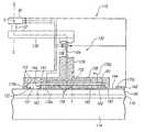
- FIG. 2is a partially schematic side elevational view of a portion of a planarizing apparatus 110 in accordance with an embodiment of the invention.
- the apparatus 110includes a planarizing pad 140 supported on a support table 114 and a sub-pad 116 in a manner generally similar to that discussed above.
- the planarizing pad 140has an upwardly facing planarizing surface 142 that supports a planarizing liquid 144 .
- the planarizing liquid 144includes a suspension of abrasive particles for mechanically removing material from a microelectronic substrate 160 .
- the abrasive particlescan be fixedly embedded in the planarizing pad 140 .
- the microelectronic substrate 160is supported by a substrate support 150 that is coupled to a carrier assembly 130 for moving the microelectronic substrate 160 relative to the planarizing pad 140 .
- the term “microelectronic substrate”refers to a microelectronic substrate material with or without an assembly of microelectronic devices or features.
- the microelectronic substrate 160is generally flat and has a generally circular planform shape with a lower surface 162 facing toward the planarizing pad 140 , an upper surface 161 facing opposite the lower surface 162 , and a side surface 163 between the upper and lower surfaces.
- the substrate support 150can include a shallow cylindrical cavity 152 for receiving the microelectronic substrate 160 .
- the cavity 152can be defined by a bearing surface 151 that faces toward the upper surface 161 of the microelectronic substrate 160 and a cavity wall or retaining surface 153 that extends downwardly from the bearing surface 151 and faces toward the side surface 163 of the microelectronic substrate 160 .
- the diameter of the cavity 152is larger than the diameter of the microelectronic substrate 160 so that at least a portion of the cavity wall 153 is spaced apart from the side surface 163 of the microelectronic substrate 160 . Accordingly, the microelectronic substrate 160 can move laterally within the cavity 152 by an amount that is limited by the cavity wall 153 .
- the substrate holder 150can include a liquid bearing 143 between the bearing surface 151 and the upper surface 161 of the microelectronic substrate 160 .
- the liquid bearing 143can reduce friction between the substrate support 150 and the upper surface 161 of the microelectronic substrate 160 by inhibiting or even eliminating direct physical contact between the two.
- the liquid in the liquid bearing 143is continuously replenished by a liquid supply conduit 154 coupled to a source (not shown) of bearing liquid.
- the liquid supply conduit 154can deliver the bearing liquid to a plenum 155 in fluid communication with a plurality of orifices 156 in the bearing surface 151 .
- the orifices 156are offset radially inwardly from the cavity wall 153 so that all the orifices 156 face directly toward the upper surface 161 of the microelectronic substrate 160 even when the microelectronic substrate 160 moves laterally within the cavity 152 . Accordingly, all the liquid supplied through the orifices 156 will flow into the liquid bearing 143 to reduce the likelihood of contact between the upper surface 161 of the microelectronic substrate 160 and the bearing surface 151 of the substrate support 150 .
- the bearing liquidhas a different chemical composition than the planarizing liquid 144 , but the bearing liquid is chemically compatible with the planarizing liquid 144 so as not to impact the performance of the planarizing liquid 144 .
- the bearing liquidcan have the same chemical composition as the planarizing liquid 144 .
- the bearing liquidcan supplement the planarizing liquid 144 already on the planarizing pad 140 .
- the bearing liquid provided through the orifices 156can be the sole source of the planarizing liquid 144 .
- the bearing liquidcan provide such functions as chemically activating the planarizing pad 140 , chemically or chemically-mechanically etching the lower surface 162 of the microelectronic substrate 160 , oxidizing the lower surface 162 of the microelectronic substrate 160 , inhibiting bonding between abrasive particles, lubricating the interface between the lower surface 162 and the planarizing pad 140 and/or other functions of planarizing liquids. All of these functions of the bearing liquid can be in addition to reducing friction between the upper surface 161 of the microelectronic substrate 160 and the substrate support 150 .
- the temperature of the bearing liquidcan be controlled to control the rate and/or manner in which material is removed from the microelectronic substrate 160 .
- the chemical reaction rate between the bearing liquid and the microelectronic substrate 160can be temperature dependent. Accordingly, the temperature of the bearing liquid can be controlled to optimize the reaction rate.
- the substrate support 150is rigidly connected to a terminal shaft 139 that is rigidly connected to a lateral arm 138 .
- the lateral arm 138can be coupled with a drive shaft 137 to an actuator 136 that orbits the lateral arm 138 and the substrate support 150 about an axis O-O, or sweeps the substrate support 150 over the planarizing surface 142 of the planarizing pad 140 . Accordingly, a point on the substrate support 150 that faces toward the periphery of the planarizing pad 140 always faces toward the periphery, even as the substrate support 150 orbits relative to the planarizing pad 140 . As a result, the portion of the liquid supply conduit 154 extending between the substrate support 150 and the lateral arm 138 need not include rotary couplings.
- the microelectronic substrate 160precesses relative to the substrate support 150 and the planarizing pad 140 because the side surface 163 of the microelectronic substrate 160 rolls along the cavity wall 153 of the substrate support 150 . Accordingly the microelectronic substrate 160 can rotate about its central axis P-P while the central axis P-P orbits relative to the substrate support 150 to describe a cylindrical volume.
- the actuator 136can apply a downward force (indicated by arrow D) to the microelectronic substrate 160 via the lateral arm 138 , the terminal shaft 139 and the substrate support 150 .
- the downward forcebiases the microelectronic substrate 160 against the planarizing pad 140 to remove material from the lower surface 162 of the microelectronic substrate 160 as the substrate support 150 moves the microelectronic substrate 160 relative to the planarizing pad 140 .
- the bearing liquidis supplied to the substrate support 150 at a pressure that produces a force on the microelectronic substrate 160 that exceeds the downward force applied by the actuator 136 . Accordingly, the bearing liquid separates the microelectronic substrate 160 from the bearing surface 151 by forming the liquid bearing 143 discussed above.
- the apparatus 110can include one or more sensors (collectively referred to as “sensors 170”) that monitor the liquid bearing 143 as the substrate support 150 moves relative to the planarizing pad 140 . In a further aspect of this embodiment, the sensors 170 can detect the thickness of the liquid bearing 143 .
- the apparatus 110can include an electrical sensor 170 a in the bearing surface 151 of the substrate support 150 opposite the microelectronic substrate 160 .
- the electrical sensor 170 acan form a portion of a capacitor circuit, along with the microelectronic substrate 160 , the substrate support 150 and the liquid bearing 143 .
- the electrical sensor 170 acan detect a change in the capacitance of the circuit as the thickness of the liquid bearing 143 changes.
- the sensor 170 acan detect the change in the conductivity, resistivity or inductance of the circuit or circuit portion as the thickness of the liquid bearing 143 changes.
- the sensor 170can detect changes in a magnetic field adjacent the microelectronic substrate 160 as the thickness of the liquid bearing 143 changes.
- the senor 170 acan be coupled to the carrier assembly 130 to form a feedback loop for automatically controlling the force applied to the microelectronic substrate 160 .
- the sensor 170 acan be coupled to a valve 158 in the liquid supply conduit 154 to control the amount and/or pressure of the liquid supplied to the liquid bearing 143 .
- the sensor 170 acan be coupled to the actuator 136 to adjust the downward force applied by the actuator 136 . In this alternate embodiment, the downward force applied by the actuator 136 can be reduced if the liquid bearing 143 becomes too thin.
- the apparatus 110can include one or more light emitters/sensors 170 b that direct light toward the microelectronic substrate 160 and receive reflections or other optical feedback from the microelectronic substrate 160 .
- the microelectronic substrate 160can include one or more notches 164 or other reflective features positioned in the side surface 163 .
- the sensor 170 bcan detect the rotation rate of the microelectronic substrate 160 within the cavity 152 based on the rate at which the sensor 170 b detects optical feedback due to the notches 164 .
- the rotation rate of the microelectronic substrate 160will decrease, and this decrease can be detected by the sensor 170 b.
- the sensor 170 bcan also be coupled to either the liquid supply conduit 154 or the actuator 136 to provide a feedback loop that operates in a manner generally similar to that discussed above with reference to the electrical sensor 170 a.
- the notch 164can extend through a portion of the side surface 163 of the microelectronic substrate 160 from the upper surface 161 to the lower surface 162 (as shown in dashed lines in FIG. 2).
- the sensor 170 bcan be positioned above the microelectronic substrate 160 (for example, in the lower surface of the substrate support 150 ) to detect an optical change as the microelectronic substrate 160 moves below.
- the notch 164can be replaced with a flat region or another indexing feature.
- the senor 170 bcan be mounted in the bearing surface 151 of the substrate support 150 , facing the upper surface 161 of the microelectronic substrate 160 .
- the sensor 170 bcan detect changes in the thickness of the liquid bearing 143 by detecting a spectral shift or an interference pattern produced when light directed toward the upper surface 161 from a light source (not shown) reflects from the upper surface 161 to the sensor 170 b.
- the incident lightcan strike the upper surface 161 at a normal or non-normal angle.
- the sensor 170 bcan detect a change in the intensity of the reflected light as the thickness of the liquid bearing changes.
- the apparatus 110can include a microphone or other acoustic sensor 170 c that detects sounds emitted by the microelectronic substrate 160 and/or the substrate support 150 as the thickness of the liquid bearing 143 changes.
- the thickness of the liquid bearing 143may become so small that the microelectronic substrate 160 intermittently adheres to and releases from the bearing surface 151 .
- the microelectronic substrate 160will tend to impinge on the cavity wall 153 when it releases from the bearing surface 151 .
- the sudden contact between the microelectronic substrate 160 and the cavity wall 153can release sonic energy that is detected by the acoustic detector 170 c.
- the acoustic sensor 170 ccan detect other sonic energy that can correlate to the thickness of the liquid bearing 143 .
- the sensor 170 ccan also include a sonic energy emitter and receiver, and can detect characteristics and/or changes in the received sonic energy that correspond to the thickness of the liquid bearing 143 .
- the sensor 170 ccan detect changes in acoustic waves reflected by the microelectronic substrate 160 , the cavity wall 153 and/or other portions of the apparatus 110 .
- the apparatus 110can include a pressure sensor 170 d in the cavity 152 .
- the pressure sensor 170 dcan detect changes in fluid pressure within the cavity 152 as the microelectronic substrate rolls along the cavity wall 153 . The changes in pressure will tend to form a regular pattern unless the microelectronic substrate 160 contacts the bearing surface, in which case the regular pattern will be disrupted.
- the pressure sensor 170 dcan detect the pattern disruption and provide an input signal to the supply conduit 154 and/or the actuator 136 in a manner similar to that discussed above.
- the sensor 170can include other devices, such as those discussed below with reference to FIG. 3.
- the substrate support 150can supply a continuous flow of bearing liquid to the interface between the bearing surface 151 and the microelectronic substrate 160 . Accordingly, the apparatus 110 can continuously control the friction between the microelectronic substrate 160 and the substrate support 150 while allowing the microelectronic substrate 160 to move in a controlled manner within the cavity 152 . As a result, the apparatus 110 can more uniformly planarize the microelectronic substrate 160 than can some conventional devices.
- a further advantage of an embodiment of the apparatus 110is that the microelectronic substrate 160 can precess relative to the planarizing pad 140 and the substrate support 150 without requiring a rotational coupling between the substrate support 150 and the lateral arm 138 . Accordingly, the apparatus 110 can more uniformly planarize the microelectronic substrate 160 while retaining a relatively simple connection between the lateral arm 138 and the substrate support 150 .
- liquid bearing 143eliminates the need for a removable film or pad between the bearing surface 151 and the microelectronic substrate 160 . Accordingly, the need for supplying, maintaining, and/or replacing such pads can be eliminated.
- Still another feature of an embodiment of the apparatus 110 shown in FIG. 2is that the characteristics of the liquid bearing 143 can be monitored with one or more sensors 170 .
- the sensors 170can be coupled to the liquid supply conduit 154 and/or the actuator 136 in a feedback loop.
- An advantage of this arrangementis that the apparatus 110 can automatically adjust the pressure and/or quantity of liquid supplied to the liquid bearing 143 and/or the downward force applied by the actuator 136 in response to signals received from the sensor 170 .
- the apparatus 110can adjust the pressure and/or quantity of liquid supplied to the liquid bearing 143 in order to change the downward force applied to the microelectronic substrate 160 .
- the sensors 170can detect “slip-out” of the microelectronic substrate 160 (i.e., an instance in which the microelectronic substrate 160 exits the cavity 152 during planarization). For example, the sensors 170 can directly detect the absence of the microelectronic substrate 160 from the cavity 152 , and/or the sensors 170 can detect a change in the characteristics of the liquid bearing 143 that correspond to a slip-out condition.
- the thickness of the liquid bearing 143can be controlled to prevent slip-out by keeping the liquid bearing 143 thick enough to prevent contact with the bearing surface 151 and thin enough that the cavity wall 155 does not rise completely above the side surface 163 of the microelectronic substrate 160 .
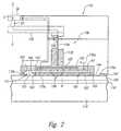
- FIG. 3is a partially schematic side elevational view of a portion of an apparatus 210 having a substrate support 250 in accordance with another embodiment of the invention.
- the substrate support 250includes a cavity 252 defined by a cavity wall 253 and a bearing surface 251 that are sized to removably receive the microelectronic substrate 160 .
- the cavity wall 253can be relatively close to the side surface 163 of the microelectronic substrate 160 (as shown in FIG. 3) or the cavity wall 253 can be spaced apart from the side surface 163 to allow the microelectronic substrate 160 more room to precess in the manner described above with reference to FIG. 2.
- the substrate support 250can include a plurality of liquid supply conduits 254 a - c and supply orifices 256 a - c (collectively referred to as “liquid supply conduits 254” and “supply orifices 256,” respectively).
- Each supply conduit 254 a - ccan be individually coupled to a source of bearing liquid at a different pressure.
- the substrate support 250can include a central liquid supply conduit 254 a connected to a central orifice 256 a, an intermediate liquid supply conduit 254 b connected to intermediate orifices 256 b, and an outer liquid supply conduit 254 c coupled to outer orifices 256 c.
- the substrate support 250can apply different downward forces to different portions of the microelectronic substrate 160 .
- This arrangementis advantageous because the spatially varying downward forces applied by the pressurized liquid can offset the naturally occurring center-to-edge planarization rate gradient that may result when the peripheral portions of the microelectronic substrate 160 move at higher velocity relative to the planarizing pad 140 than do the central portions of the microelectronic substrate 160 .
- the substrate support. 250can include a plurality of relief channels 257 positioned radially outwardly from the liquid supply conduits 254 and the orifices 256 .
- the relief channels 257extend through the cavity wall 253 from the region inside the cavity 252 to a region outside the cavity 252 . Accordingly, the relief channels 257 can regulate the pressure within the cavity 252 by allowing a desired amount of liquid to exit the cavity and can accordingly regulate the thickness of a liquid bearing 243 that forms between the upper surface 161 of the microelectronic substrate 160 and the bearing surface 251 of the substrate support 250 .
- the relief channels 257can also provide a passage through which the planarizing liquid can flow to the planarizing pad 140 .
- the substrate support 250can include a vacuum conduit 280 in fluid communication with one or more vacuum orifices 283 positioned in the bearing surface 251 of the substrate support 250 .
- the vacuum conduit 280can be coupled to a vacuum source (not shown) to remove a portion of the fluid from the liquid bearing 243 .
- the amount of liquid removed through the vacuum conduit 280can be controlled (or stopped) to control the thickness of the liquid bearing 243 .
- the rate at which liquid is removed through the vacuum conduit 280can be less than, greater than or equal to the rate at which liquid is supplied through the liquid supply conduit 254 to increase, decrease or leave unchanged, respectively, the thickness of the liquid bearing 243 .
- the vacuum orifices 283can be positioned radially outwardly from the supply orifices 256 so the bearing fluid flows toward the vacuum orifices 283 under centrifugal force as the substrate support 250 orbits.
- the relative positions of the supply orifices 256 and the vacuum orifices 283can be different in other embodiments.
- the vacuum conduit 280can also remove particulate matter from the upper surface 161 of the microelectronic substrate 160 .
- the liquid provided by the liquid supply conduits 254can entrain residual foreign matter on the upper surface 161 of the microelectronic substrate 160 .
- the liquidis evacuated through the vacuum conduit 280 , it carries the foreign matter with it and prevents the foreign matter from eventually reaching the lower surface 162 of the microelectronic substrate 160 and/or the planarizing surface 142 of the planarizing pad 140 .
- the vacuum conduit 280can remove the abraded particles before they reach the planarizing pad 140 .
- the apparatus 210can include a particle sensor 281 in fluid communication with the vacuum conduit 280 to detect particles entrained in the fluid passing through the vacuum conduit 280 .
- a change in the size, size distribution, number, concentration and/or other characteristics of the particulate matter detected by the particle sensor 281can indicate the state of the liquid bearing 243 . For example, if the number and/or median size of particles detected by the particle sensor 281 increases, the upper surface 161 of the substrate may have contacted the bearing surface 251 of the substrate support 250 , indicating that the liquid bearing 243 is too thin.
- the particle detector 281can be operatively coupled to the liquid supply conduits 254 and/or the actuator 136 to control the thickness of the fluid bearing 243 in a manner generally similar to that discussed above with reference to FIG. 2.
- the apparatus 210can include one or more of the sensors 170 discussed above with reference to FIG. 2 in addition to or in lieu of the particle detector 281 .
- the apparatus 210can include a filter 282 in fluid communication with the vacuum conduit 280 .
- the particle filter 282can remove particulates from the fluid passing through the vacuum conduit 280 .
- the filter 282can remove enough particles to allow the fluid to be recycled for re-use with either the same apparatus 210 or a different apparatus.
- An advantage of an embodiment of the apparatus 210 discussed above with reference to FIG. 3is that the vacuum conduit 280 can control the thickness of the fluid bearing 243 .
- the vacuum conduit 280can also remove particulates from the fluid forming the fluid bearing 243 before the particulates reach the interface between the lower surface 162 of the microelectronic substrate 160 and the planarizing surface 142 of the planarizing pad 140 . Accordingly, the apparatus 210 can reduce the likelihood for forming scratches or other asperities on the lower surface 162 of the microelectronic substrate 160 .
- FIG. 4is a partially schematic cross-sectional view of a rotary planarizing machine 310 with a generally circular platen or table 320 , a carrier assembly 330 , a planarizing pad 340 positioned on the platen 320 and a planarizing fluid 344 on the planarizing pad 340 .
- the planarizing machine 310may also have an under-pad 325 attached to an upper surface 322 of the platen 320 for supporting the planarizing pad 340 .
- a drive 1 S assembly 326rotates (arrow “F”) and/or reciprocates (arrow “G”), the platen 320 to move the planarizing pad 340 during planarization.
- the carrier assembly 330controls and protects the microelectronic substrate 160 during planarization.
- the carrier assembly 330typically has a substrate holder 350 that supports the microelectronic substrate 160 and biases the microelectronic substrate 160 against the planarizing pad 340 in a manner generally similar to that discussed above with reference to FIGS. 2 and/or 3 .
- a drive assembly 336 of the carrier assembly 330typically orbits and/or translates the substrate holder 350 (arrows “H” and “I”, respectively), also in a manner similar to that discussed above with reference to FIGS. 2 and/or 3 .
- the drive assembly 336can also rotate the substrate holder 350 about its central axis.
- the substrate holder 350is the same as the substrate holders 150 and 250 described above with respect to FIGS. 2 and 3.
- the carrier assembly 330presses the microelectronic substrate 160 against a planarizing surface 342 of the planarizing pad 340 .
- the platen 320 and/or the substrate holder 350then move relative to one another to translate the microelectronic substrate 160 across the planarizing surface 342 .
- abrasive particles and/or chemicals in the planarizing pad 340 and/or the planarizing liquid 344remove material from the surface of the microelectronic substrate 160 .
Landscapes
- Engineering & Computer Science (AREA)
- Mechanical Engineering (AREA)
- Physics & Mathematics (AREA)
- General Physics & Mathematics (AREA)
- Automation & Control Theory (AREA)
- Cleaning Or Drying Semiconductors (AREA)
Abstract
Description
- This invention relates to methods and apparatuses for supporting microelectronic substrates during planarization.[0001]
- Mechanical and chemical-mechanical planarization processes (collectively “CMP”) are used in the manufacturing of electronic devices for forming a flat surface on semiconductor wafers, field emission displays and many other microelectronic-device substrate assemblies. CMP processes generally remove material from a substrate or substrate assembly to create a highly planar surface at a precise elevation in the layers of material on the substrate. FIG. 1 schematically illustrates an existing web-format-planarizing[0002]
machine 10 for planarizing asubstrate 60. The planarizingmachine 10 has a support table14 with asub-pad 16 at a workstation where an operative portion “A” of aplanarizing pad 40 is positioned. Thesub-pad 16 is generally a rigid plate to provide a flat, solid surface to which a particular section of theplanarizing pad 40 may be secured during planarization. - The planarizing[0003]
machine 10 also has a plurality of rollers to guide, position and hold the planarizingpad 40 over thesub-pad 16. The rollers include asupply roller 20,idler rollers 21,guide rollers 22, and a take-up roller 23. Thesupply roller 20 carries an unused or pre-operative portion of the planarizingpad 40, and the take-up roller 23 carries a used or post-operative portion of the planarizingpad 40. Additionally, theleft idler roller 21 and theupper guide roller 22 stretch theplanarizing pad 40 over thesub-pad 16 to hold the planarizingpad 40 stationary during operation. A motor (not shown) drives at least one of thesupply roller 20 and the take-up roller 23 to sequentially advance theplanarizing pad 40 across thesub-pad 16. Accordingly, clean pre-operative sections of the planarizingpad 40 may be quickly substituted for used sections to provide a consistent surface for planarizing and/or cleaning thesubstrate 60. - The web-format-planarizing[0004]
machine 10 also has acarrier assembly 30 that controls and protects thesubstrate 60 during planarization. Thecarrier assembly 30 generally has a substrate holder50 to pick up, hold and release thesubstrate 60 at appropriate stages of the planarizing process. The substrate holder50 engages aretainer ring 31 that surrounds themicroelectronic substrate 60 and restricts lateral motion of themicroelectronic substrate 60 relative to the substrate holder50.Several nozzles 33 attached to the substrate holder50 dispense a planarizingsolution 44 onto a planarizingsurface 42 of theplanarizing pad 40. Thecarrier assembly 30 also generally has asupport gantry 34 carrying adrive assembly 35 that can translate along thegantry 34. Thedrive assembly 35 generally has anactuator 36, adrive shaft 37 coupled to theactuator 36, and anarm 38 projecting from thedrive shaft 37. Thearm 38 carries the substrate holder50 via a terminal shaft39 such that thedrive assembly 35 orbits the substrate holder50 about an axis B-B (as indicated by arrow “R1”). The terminal shaft39 may also rotate the substrate holder50 about its central axis C-C (as indicated by arrow “R2”). - The[0005]
planarizing pad 40 and theplanarizing solution 44 define a planarizing medium that mechanically and/or chemically-mechanically removes material from the surface of thesubstrate 60. The planarizingpad 40 used in the web-format planarizingmachine 10 is typically a fixed-abrasive planarizing pad in which abrasive particles are fixedly bonded to a suspension material. In fixed-abrasive applications, the planarizing solution is a “clean solution” without abrasive particles. In other applications, theplanarizing pad 40 may be a non-abrasive pad without abrasive particles. The planarizingsolutions 44 used with the non-abrasive planarizing pads are typically CMP slurries with abrasive particles and chemicals. - To planarize the[0006]
substrate 60 with the planarizingmachine 10, thecarrier assembly 30 presses thesubstrate 60 against the planarizingsurface 42 of theplanarizing pad 40 in the presence of theplanarizing solution 44. Thedrive assembly 35 then orbits the substrate holder50 about the axis B-B and optionally rotates the substrate holder50 about the axis C-C to translate thesubstrate 60 across theplanarizing surface 42. As a result, the abrasive particles and/or the chemicals in the planarizing medium remove material from the surface of thesubstrate 60. - The CMP processes should consistently and accurately produce a uniformly planar surface on the[0007]
substrate 60 to enable precise fabrication of circuits and photo-patterns. During the fabrication of transistors, contacts, interconnects and other features, many substrates or substrate assemblies develop large “step heights” that create a highly topographic surface across the substrate assembly. Yet, as the density of integrated circuits increases, it is necessary to have a planar substrate surface at several intermediate stages during the fabrication of devices on a substrate assembly because non-uniform substrate surfaces significantly increase the difficulty of forming sub-micron features. For example, it is difficult to accurately focus photo patterns to within tolerances approaching 0.1 micron on non-uniform substrate surfaces because sub-micron photolithographic equipment generally has a very limited depth of field. Thus, CMP processes are often used to transform a topographical substrate surface into a highly uniform, planar substrate surface. - One problem with some conventional CMP techniques is that the[0008]
carrier assembly 30 may not apply a uniform downward force on thesubstrate 60. Accordingly, the planarized surface of thesubstrate 60 may develop non-uniformities that can adversely affect subsequent processing steps. One approach to address this problem is to rotate thesubstrate 60 and the substrate holder50 as a unit about axis C-C, but a drawback with this approach is that it increases the mechanical complexity of the substrate holder50 and thecarrier assembly 30. This approach particularly increases the mechanical complexity if thecarrier assembly 30 includes fluid couplings between thearm 38 and the substrate holder50 (for example, to supply the planarizingliquid 44 to the nozzles33). - Another problem with some conventional devices is that the[0009]
retainer ring 31 can wipe the planarizingliquid 44 from theplanarizing pad 40 as the substrate carrier50 and thesubstrate 60 move across theplanarizing pad 40. Accordingly, theplanarizing liquid 44 may not uniformly coat the lower surface of thesubstrate 60, which can reduce the planarizing rate and/or the planarity of thesubstrate 60. Still another problem is that thecarrier assembly 30 can include a disposable film at the interface between the substrate holder50 and thesubstrate 60 to grip thesubstrate 60. The disposable film must be periodically replaced, which increases the time and expense required to maintain theapparatus 10. - One approach for addressing some of the foregoing problems is to direct pressurized air against the rear surface of the[0010]
substrate 60 during planarization. For example, U.S. Pat. No. 5,762,539 to Nakashiba et al. discloses a carrier apparatus that directs several jets of compressed air at different pressures toward the rear surface of the substrate to bias the substrate against the polishing pad while the carrier rotates relative to the polishing pad. One drawback with this approach is that the arrangement for supplying compressed air to the carrier may be complex and subject to leaks because it includes rotary couplings that direct the compressed air to the rotating carrier. A further disadvantage is that the compressed air can evaporate the planarizing liquid, reducing the effectiveness of the planarizing medium. When the planarizing liquid includes an abrasive slurry, the compressed air can evaporate the liquid portion of the slurry, causing the abrasive particles in the slurry to agglomerate. Furthermore, the thickness of the air cushion between the carrier and substrate can be difficult to control because the air has a relatively low viscosity. - U.S. Pat. No. 4,869,779 to Acheson discloses directing planarizing liquid upwardly from beneath the polishing pad against the front surface of the substrate. One drawback with this approach is that the carrier that supports the substrate relative to the polishing pad “floats” over the polishing pad. Accordingly, the apparatus cannot easily vary the downward force between the substrate and the polishing pad.[0011]
- U.S. Pat. No. 4,256,535 to Banks discloses placing a drop of water between the rear surface of the substrate and the carrier. One drawback with this approach is that the water can be squeezed out from between the substrate and the carrier during planarization. Accordingly, the carrier can contact the rear surface of the substrate and abrade material from the substrate. The abraded material can then become caught between the downwardly facing surface of the substrate and the planarizing pad, potentially scratching the surface of the substrate. Another drawback is that the substrate rotates freely relative to the holder, which can reduce control over the motion of the substrate.[0012]
- U.S. Pat. No. 4,373,991, also to Banks, discloses directing a continuous flow of pressurized water against the backside of the substrate. One problem with this approach is that the substrate carrier rotates relative to its support arm, increasing the mechanical complexity of the apparatus, as discussed above.[0013]
- The present invention is directed toward methods and apparatuses for planarizing microelectronic substrates. A method in accordance with one aspect of the invention includes facing a first surface of the microelectronic substrate toward a planarizing surface of a planarizing pad and biasing the microelectronic substrate toward the planarizing surface by directing a flow of planarizing liquid toward a second surface of the microelectronic substrate facing generally opposite the first surface. In one embodiment, the planarizing liquid includes water and at least one of an etchant, oxidant, surfactant, abrasive particle or other chemical compound to control the removal of material from the substrate. The method can further include disposing the planarizing liquid between the first surface of the microelectronic substrate and the planarizing pad by moving one or the other of the microelectronic substrate and the planarizing pad. The rate and/or manner of material removal from the microelectronic substrate is controlled by engaging the planarizing liquid with the first surface of the microelectronic substrate.[0014]
- In another aspect of the invention, the method can include positioning the microelectronic substrate proximate to a substrate support and biasing the microelectronic substrate toward the planarizing surface by directing a flow of liquid toward the second surface of the microelectronic substrate. The method can further include moving at least one of the microelectronic substrate and the planarizing pad relative to the other and monitoring a characteristic of a liquid layer that forms between the microelectronic substrate and the substrate support, for example by monitoring the pressure of the liquid or electrical characteristics of the liquid. In a further aspect of the invention, a portion of the liquid can be removed from the second surface of the microelectronic substrate to control the pressure against the second surface. The removed liquid can be monitored for the presence of particulate matter and, in still a further aspect of the invention, the particulate matter can be removed and the liquid recycled.[0015]
- The present invention is also directed toward an apparatus for planarizing a microelectronic substrate having a first surface and a second surface opposite the first surface. In one aspect of the invention, the apparatus can include a planarizing pad having a planarizing surface configured to engage the first surface of the microelectronic substrate and a substrate support having a retaining surface positioned to at least restrict lateral motion of the microelectronic substrate relative to the planarizing pad. The substrate support can have at least one fluid orifice directed toward the second surface of the microelectronic substrate and coupled to a source of planarizing liquid selected to control a rate and/or manner of material removed from the microelectronic substrate when the microelectronic substrate engages the planarizing pad and one of the microelectronic substrate and the planarizing pad moves relative to the other.[0016]
- In another aspect of the invention, the apparatus can include a sensor positioned to monitor a characteristic of a liquid layer between the second surface of the microelectronic substrate and the substrate support. In still another aspect of the invention, the apparatus can include a vacuum source having a removal aperture in fluid communication with the substrate support for removing a portion of the liquid proximate to the second surface of the microelectronic substrate.[0017]
- FIG. 1 is a partially schematic side elevational view of a planarizing apparatus in accordance with the prior art.[0018]
- FIG. 2 is a partially schematic side elevational view of a portion of a planarizing apparatus that controls motion of a microelectronic substrate with a liquid bearing in accordance with an embodiment of the invention.[0019]
- FIG. 3 is a partially schematic side elevational view of a portion of a planarizing apparatus that controls motion of a microelectronic substrate with a liquid bearing in accordance with another embodiment of the invention.[0020]
- FIG. 4 is a partially schematic side elevational view of a rotary apparatus having a liquid bearing in accordance with yet another embodiment of the invention.[0021]
- The present disclosure describes methods and apparatuses for chemical and/or chemical-mechanical planarizing of substrates and substrate assemblies used in the fabrication of microelectronic devices. Many specific details of certain embodiments of the invention are set forth in the following description and in FIGS.[0022]2-4 to provide a thorough understanding of these embodiments. One skilled in the art, however, will understand that the present invention may have additional embodiments, or that the invention may be practiced without several of the details described below.
- FIG. 2 is a partially schematic side elevational view of a portion of a[0023]
planarizing apparatus 110 in accordance with an embodiment of the invention. Theapparatus 110 includes aplanarizing pad 140 supported on a support table114 and a sub-pad116 in a manner generally similar to that discussed above. Theplanarizing pad 140 has an upwardly facingplanarizing surface 142 that supports aplanarizing liquid 144. In one aspect of this embodiment, theplanarizing liquid 144 includes a suspension of abrasive particles for mechanically removing material from amicroelectronic substrate 160. Alternatively, the abrasive particles can be fixedly embedded in theplanarizing pad 140. In either embodiment, themicroelectronic substrate 160 is supported by asubstrate support 150 that is coupled to acarrier assembly 130 for moving themicroelectronic substrate 160 relative to theplanarizing pad 140. As used herein, the term “microelectronic substrate” refers to a microelectronic substrate material with or without an assembly of microelectronic devices or features. - In one embodiment, the[0024]
microelectronic substrate 160 is generally flat and has a generally circular planform shape with alower surface 162 facing toward theplanarizing pad 140, anupper surface 161 facing opposite thelower surface 162, and aside surface 163 between the upper and lower surfaces. Thesubstrate support 150 can include a shallowcylindrical cavity 152 for receiving themicroelectronic substrate 160. Thecavity 152 can be defined by a bearingsurface 151 that faces toward theupper surface 161 of themicroelectronic substrate 160 and a cavity wall or retainingsurface 153 that extends downwardly from the bearingsurface 151 and faces toward theside surface 163 of themicroelectronic substrate 160. In one aspect of this embodiment, the diameter of thecavity 152 is larger than the diameter of themicroelectronic substrate 160 so that at least a portion of thecavity wall 153 is spaced apart from theside surface 163 of themicroelectronic substrate 160. Accordingly, themicroelectronic substrate 160 can move laterally within thecavity 152 by an amount that is limited by thecavity wall 153. - In a further aspect of this embodiment, the[0025]
substrate holder 150 can include aliquid bearing 143 between thebearing surface 151 and theupper surface 161 of themicroelectronic substrate 160. Theliquid bearing 143 can reduce friction between thesubstrate support 150 and theupper surface 161 of themicroelectronic substrate 160 by inhibiting or even eliminating direct physical contact between the two. In one embodiment, the liquid in theliquid bearing 143 is continuously replenished by aliquid supply conduit 154 coupled to a source (not shown) of bearing liquid. Theliquid supply conduit 154 can deliver the bearing liquid to aplenum 155 in fluid communication with a plurality oforifices 156 in thebearing surface 151. In one aspect of this embodiment, theorifices 156 are offset radially inwardly from thecavity wall 153 so that all theorifices 156 face directly toward theupper surface 161 of themicroelectronic substrate 160 even when themicroelectronic substrate 160 moves laterally within thecavity 152. Accordingly, all the liquid supplied through theorifices 156 will flow into theliquid bearing 143 to reduce the likelihood of contact between theupper surface 161 of themicroelectronic substrate 160 and thebearing surface 151 of thesubstrate support 150. - In one embodiment, the bearing liquid has a different chemical composition than the[0026]
planarizing liquid 144, but the bearing liquid is chemically compatible with theplanarizing liquid 144 so as not to impact the performance of theplanarizing liquid 144. Alternatively, the bearing liquid can have the same chemical composition as theplanarizing liquid 144. For example, the bearing liquid can supplement theplanarizing liquid 144 already on theplanarizing pad 140. Alternatively, the bearing liquid provided through theorifices 156 can be the sole source of theplanarizing liquid 144. Accordingly, the bearing liquid can provide such functions as chemically activating theplanarizing pad 140, chemically or chemically-mechanically etching thelower surface 162 of themicroelectronic substrate 160, oxidizing thelower surface 162 of themicroelectronic substrate 160, inhibiting bonding between abrasive particles, lubricating the interface between thelower surface 162 and theplanarizing pad 140 and/or other functions of planarizing liquids. All of these functions of the bearing liquid can be in addition to reducing friction between theupper surface 161 of themicroelectronic substrate 160 and thesubstrate support 150. - In one embodiment, the temperature of the bearing liquid can be controlled to control the rate and/or manner in which material is removed from the[0027]
microelectronic substrate 160. For example, when the bearing liquid chemically interacts with themicroelectronic substrate 160 to remove material from the surface of the microelectronic substrate, the chemical reaction rate between the bearing liquid and themicroelectronic substrate 160 can be temperature dependent. Accordingly, the temperature of the bearing liquid can be controlled to optimize the reaction rate. - In one embodiment, the[0028]
substrate support 150 is rigidly connected to aterminal shaft 139 that is rigidly connected to alateral arm 138. Thelateral arm 138 can be coupled with adrive shaft 137 to anactuator 136 that orbits thelateral arm 138 and thesubstrate support 150 about an axis O-O, or sweeps thesubstrate support 150 over theplanarizing surface 142 of theplanarizing pad 140. Accordingly, a point on thesubstrate support 150 that faces toward the periphery of theplanarizing pad 140 always faces toward the periphery, even as thesubstrate support 150 orbits relative to theplanarizing pad 140. As a result, the portion of theliquid supply conduit 154 extending between thesubstrate support 150 and thelateral arm 138 need not include rotary couplings. - As the[0029]
substrate support 150 orbits or translates, themicroelectronic substrate 160 precesses relative to thesubstrate support 150 and theplanarizing pad 140 because theside surface 163 of themicroelectronic substrate 160 rolls along thecavity wall 153 of thesubstrate support 150. Accordingly themicroelectronic substrate 160 can rotate about its central axis P-P while the central axis P-P orbits relative to thesubstrate support 150 to describe a cylindrical volume. - In one embodiment, the[0030]
actuator 136 can apply a downward force (indicated by arrow D) to themicroelectronic substrate 160 via thelateral arm 138, theterminal shaft 139 and thesubstrate support 150. The downward force biases themicroelectronic substrate 160 against theplanarizing pad 140 to remove material from thelower surface 162 of themicroelectronic substrate 160 as thesubstrate support 150 moves themicroelectronic substrate 160 relative to theplanarizing pad 140. - In one aspect of this embodiment, the bearing liquid is supplied to the[0031]
substrate support 150 at a pressure that produces a force on themicroelectronic substrate 160 that exceeds the downward force applied by theactuator 136. Accordingly, the bearing liquid separates themicroelectronic substrate 160 from the bearingsurface 151 by forming theliquid bearing 143 discussed above. Theapparatus 110 can include one or more sensors (collectively referred to as “sensors 170”) that monitor theliquid bearing 143 as thesubstrate support 150 moves relative to theplanarizing pad 140. In a further aspect of this embodiment, the sensors170 can detect the thickness of theliquid bearing 143. For example, theapparatus 110 can include anelectrical sensor 170ain thebearing surface 151 of thesubstrate support 150 opposite themicroelectronic substrate 160. In one aspect of this embodiment, theelectrical sensor 170acan form a portion of a capacitor circuit, along with themicroelectronic substrate 160, thesubstrate support 150 and theliquid bearing 143. Theelectrical sensor 170acan detect a change in the capacitance of the circuit as the thickness of theliquid bearing 143 changes. Alternatively, thesensor 170a can detect the change in the conductivity, resistivity or inductance of the circuit or circuit portion as the thickness of theliquid bearing 143 changes. In still another embodiment, the sensor170 can detect changes in a magnetic field adjacent themicroelectronic substrate 160 as the thickness of theliquid bearing 143 changes. - In any of the foregoing embodiments, the[0032]
sensor 170acan be coupled to thecarrier assembly 130 to form a feedback loop for automatically controlling the force applied to themicroelectronic substrate 160. For example, thesensor 170acan be coupled to avalve 158 in theliquid supply conduit 154 to control the amount and/or pressure of the liquid supplied to theliquid bearing 143. When theliquid bearing 143 is too thin, the amount of liquid supplied by theliquid supply conduit 154 and/or the pressure of the liquid can be increased by automatically adjusting thevalve 158 in response to signals received from thesensor 170a.Alternatively, thesensor 170acan be coupled to theactuator 136 to adjust the downward force applied by theactuator 136. In this alternate embodiment, the downward force applied by theactuator 136 can be reduced if theliquid bearing 143 becomes too thin. - In an alternate embodiment, the[0033]
apparatus 110 can include one or more light emitters/sensors 170bthat direct light toward themicroelectronic substrate 160 and receive reflections or other optical feedback from themicroelectronic substrate 160. For example, themicroelectronic substrate 160 can include one ormore notches 164 or other reflective features positioned in theside surface 163. Thesensor 170bcan detect the rotation rate of themicroelectronic substrate 160 within thecavity 152 based on the rate at which thesensor 170bdetects optical feedback due to thenotches 164. Accordingly, if theliquid bearing 143 becomes so thin that theupper surface 161 of themicroelectronic substrate 160 touches the bearingsurface 151, the rotation rate of themicroelectronic substrate 160 will decrease, and this decrease can be detected by thesensor 170b.Thesensor 170bcan also be coupled to either theliquid supply conduit 154 or theactuator 136 to provide a feedback loop that operates in a manner generally similar to that discussed above with reference to theelectrical sensor 170a. - In other embodiments, the[0034]
sensor 170band/or themicroelectronic substrate 160 can have other configurations. For example, thenotch 164 can extend through a portion of theside surface 163 of themicroelectronic substrate 160 from theupper surface 161 to the lower surface162 (as shown in dashed lines in FIG. 2). Thesensor 170bcan be positioned above the microelectronic substrate160 (for example, in the lower surface of the substrate support150) to detect an optical change as themicroelectronic substrate 160 moves below. Alternatively, thenotch 164 can be replaced with a flat region or another indexing feature. - In another embodiment, the[0035]
sensor 170bcan be mounted in thebearing surface 151 of thesubstrate support 150, facing theupper surface 161 of themicroelectronic substrate 160. In one aspect of the embodiment, thesensor 170bcan detect changes in the thickness of theliquid bearing 143 by detecting a spectral shift or an interference pattern produced when light directed toward theupper surface 161 from a light source (not shown) reflects from theupper surface 161 to thesensor 170b.The incident light can strike theupper surface 161 at a normal or non-normal angle. Alternatively, thesensor 170bcan detect a change in the intensity of the reflected light as the thickness of the liquid bearing changes. - In still another embodiment, the[0036]
apparatus 110 can include a microphone or otheracoustic sensor 170cthat detects sounds emitted by themicroelectronic substrate 160 and/or thesubstrate support 150 as the thickness of theliquid bearing 143 changes. For example, the thickness of theliquid bearing 143 may become so small that themicroelectronic substrate 160 intermittently adheres to and releases from the bearingsurface 151. Themicroelectronic substrate 160 will tend to impinge on thecavity wall 153 when it releases from the bearingsurface 151. The sudden contact between themicroelectronic substrate 160 and thecavity wall 153 can release sonic energy that is detected by theacoustic detector 170c.Alternatively, theacoustic sensor 170ccan detect other sonic energy that can correlate to the thickness of theliquid bearing 143. For example, thesensor 170ccan also include a sonic energy emitter and receiver, and can detect characteristics and/or changes in the received sonic energy that correspond to the thickness of theliquid bearing 143. In a further aspect of this embodiment, thesensor 170ccan detect changes in acoustic waves reflected by themicroelectronic substrate 160, thecavity wall 153 and/or other portions of theapparatus 110. - In yet another embodiment, the[0037]
apparatus 110 can include apressure sensor 170din thecavity 152. Thepressure sensor 170dcan detect changes in fluid pressure within thecavity 152 as the microelectronic substrate rolls along thecavity wall 153. The changes in pressure will tend to form a regular pattern unless themicroelectronic substrate 160 contacts the bearing surface, in which case the regular pattern will be disrupted. Thepressure sensor 170dcan detect the pattern disruption and provide an input signal to thesupply conduit 154 and/or theactuator 136 in a manner similar to that discussed above. In other embodiments, the sensor170 can include other devices, such as those discussed below with reference to FIG. 3. - One feature of an embodiment of the[0038]
apparatus 110 discussed above with reference to FIG. 2 is that thesubstrate support 150 can supply a continuous flow of bearing liquid to the interface between thebearing surface 151 and themicroelectronic substrate 160. Accordingly, theapparatus 110 can continuously control the friction between themicroelectronic substrate 160 and thesubstrate support 150 while allowing themicroelectronic substrate 160 to move in a controlled manner within thecavity 152. As a result, theapparatus 110 can more uniformly planarize themicroelectronic substrate 160 than can some conventional devices. - A further advantage of an embodiment of the[0039]
apparatus 110 is that themicroelectronic substrate 160 can precess relative to theplanarizing pad 140 and thesubstrate support 150 without requiring a rotational coupling between thesubstrate support 150 and thelateral arm 138. Accordingly, theapparatus 110 can more uniformly planarize themicroelectronic substrate 160 while retaining a relatively simple connection between thelateral arm 138 and thesubstrate support 150. - Yet a further advantage of an embodiment of the[0040]
apparatus 110 is that theliquid bearing 143 eliminates the need for a removable film or pad between thebearing surface 151 and themicroelectronic substrate 160. Accordingly, the need for supplying, maintaining, and/or replacing such pads can be eliminated. - Still another feature of an embodiment of the[0041]
apparatus 110 shown in FIG. 2 is that the characteristics of theliquid bearing 143 can be monitored with one or more sensors170. The sensors170 can be coupled to theliquid supply conduit 154 and/or theactuator 136 in a feedback loop. An advantage of this arrangement is that theapparatus 110 can automatically adjust the pressure and/or quantity of liquid supplied to theliquid bearing 143 and/or the downward force applied by theactuator 136 in response to signals received from the sensor170. In one aspect of this arrangement, theapparatus 110 can adjust the pressure and/or quantity of liquid supplied to theliquid bearing 143 in order to change the downward force applied to themicroelectronic substrate 160. Either arrangement can accordingly reduce the likelihood that themicroelectronic substrate 160 will directly contact the bearingsurface 151. Another advantage of these arrangements is that the sensors170 can detect “slip-out” of the microelectronic substrate160 (i.e., an instance in which themicroelectronic substrate 160 exits thecavity 152 during planarization). For example, the sensors170 can directly detect the absence of themicroelectronic substrate 160 from thecavity 152, and/or the sensors170 can detect a change in the characteristics of theliquid bearing 143 that correspond to a slip-out condition. In an alternate arrangement, the thickness of theliquid bearing 143 can be controlled to prevent slip-out by keeping theliquid bearing 143 thick enough to prevent contact with the bearingsurface 151 and thin enough that thecavity wall 155 does not rise completely above theside surface 163 of themicroelectronic substrate 160. - FIG. 3 is a partially schematic side elevational view of a portion of an[0042]
apparatus 210 having asubstrate support 250 in accordance with another embodiment of the invention. Thesubstrate support 250 includes acavity 252 defined by acavity wall 253 and abearing surface 251 that are sized to removably receive themicroelectronic substrate 160. Thecavity wall 253 can be relatively close to theside surface 163 of the microelectronic substrate160 (as shown in FIG. 3) or thecavity wall 253 can be spaced apart from theside surface 163 to allow themicroelectronic substrate 160 more room to precess in the manner described above with reference to FIG. 2. - In either of the above embodiments, the[0043]
substrate support 250 can include a plurality of liquid supply conduits254a-cand supply orifices256a-c(collectively referred to as “liquid supply conduits 254” and “supply orifices 256,” respectively). Each supply conduit254a-ccan be individually coupled to a source of bearing liquid at a different pressure. For example, thesubstrate support 250 can include a centralliquid supply conduit 254aconnected to a central orifice256a,an intermediateliquid supply conduit 254bconnected tointermediate orifices 256b,and an outer liquid supply conduit254ccoupled toouter orifices 256c.Accordingly, thesubstrate support 250 can apply different downward forces to different portions of themicroelectronic substrate 160. This arrangement is advantageous because the spatially varying downward forces applied by the pressurized liquid can offset the naturally occurring center-to-edge planarization rate gradient that may result when the peripheral portions of themicroelectronic substrate 160 move at higher velocity relative to theplanarizing pad 140 than do the central portions of themicroelectronic substrate 160. - In another aspect of the embodiment shown in FIG. 3, the substrate support.[0044]250 can include a plurality of
relief channels 257 positioned radially outwardly from the liquid supply conduits254 and the orifices256. In one embodiment, therelief channels 257 extend through thecavity wall 253 from the region inside thecavity 252 to a region outside thecavity 252. Accordingly, therelief channels 257 can regulate the pressure within thecavity 252 by allowing a desired amount of liquid to exit the cavity and can accordingly regulate the thickness of aliquid bearing 243 that forms between theupper surface 161 of themicroelectronic substrate 160 and thebearing surface 251 of thesubstrate support 250. When the liquid supplied to theliquid bearing 243 includes a planarizing liquid, therelief channels 257 can also provide a passage through which the planarizing liquid can flow to theplanarizing pad 140. - In another aspect of the embodiment shown in FIG. 3, the[0045]
substrate support 250 can include avacuum conduit 280 in fluid communication with one ormore vacuum orifices 283 positioned in thebearing surface 251 of thesubstrate support 250. Thevacuum conduit 280 can be coupled to a vacuum source (not shown) to remove a portion of the fluid from theliquid bearing 243. In one aspect of this embodiment, the amount of liquid removed through thevacuum conduit 280 can be controlled (or stopped) to control the thickness of theliquid bearing 243. For example, the rate at which liquid is removed through thevacuum conduit 280 can be less than, greater than or equal to the rate at which liquid is supplied through the liquid supply conduit254 to increase, decrease or leave unchanged, respectively, the thickness of theliquid bearing 243. The vacuum orifices283 can be positioned radially outwardly from the supply orifices256 so the bearing fluid flows toward thevacuum orifices 283 under centrifugal force as thesubstrate support 250 orbits. Alternatively, the relative positions of the supply orifices256 and thevacuum orifices 283 can be different in other embodiments. - The[0046]
vacuum conduit 280 can also remove particulate matter from theupper surface 161 of themicroelectronic substrate 160. For example, at the beginning of the planarization operation, the liquid provided by the liquid supply conduits254 can entrain residual foreign matter on theupper surface 161 of themicroelectronic substrate 160. When the liquid is evacuated through thevacuum conduit 280, it carries the foreign matter with it and prevents the foreign matter from eventually reaching thelower surface 162 of themicroelectronic substrate 160 and/or theplanarizing surface 142 of theplanarizing pad 140. Alternatively, if theliquid bearing 243 becomes so thin that theupper surface 161 of themicroelectronic substrate 160 contacts thebearing surface 251 of thesubstrate support 250 and abrades particles from either theupper surface 161 or thebearing surface 251, thevacuum conduit 280 can remove the abraded particles before they reach theplanarizing pad 140. - In still a further aspect of this embodiment, the[0047]
apparatus 210 can include aparticle sensor 281 in fluid communication with thevacuum conduit 280 to detect particles entrained in the fluid passing through thevacuum conduit 280. A change in the size, size distribution, number, concentration and/or other characteristics of the particulate matter detected by theparticle sensor 281 can indicate the state of theliquid bearing 243. For example, if the number and/or median size of particles detected by theparticle sensor 281 increases, theupper surface 161 of the substrate may have contacted thebearing surface 251 of thesubstrate support 250, indicating that theliquid bearing 243 is too thin. In a further aspect of this embodiment, theparticle detector 281 can be operatively coupled to the liquid supply conduits254 and/or theactuator 136 to control the thickness of thefluid bearing 243 in a manner generally similar to that discussed above with reference to FIG. 2. Alternatively, theapparatus 210 can include one or more of the sensors170 discussed above with reference to FIG. 2 in addition to or in lieu of theparticle detector 281. - In still another aspect of the embodiment shown in FIG. 3, the[0048]
apparatus 210 can include afilter 282 in fluid communication with thevacuum conduit 280. Theparticle filter 282 can remove particulates from the fluid passing through thevacuum conduit 280. For example, thefilter 282 can remove enough particles to allow the fluid to be recycled for re-use with either thesame apparatus 210 or a different apparatus. - An advantage of an embodiment of the[0049]
apparatus 210 discussed above with reference to FIG. 3 is that thevacuum conduit 280 can control the thickness of thefluid bearing 243. Thevacuum conduit 280 can also remove particulates from the fluid forming thefluid bearing 243 before the particulates reach the interface between thelower surface 162 of themicroelectronic substrate 160 and theplanarizing surface 142 of theplanarizing pad 140. Accordingly, theapparatus 210 can reduce the likelihood for forming scratches or other asperities on thelower surface 162 of themicroelectronic substrate 160. - FIG. 4 is a partially schematic cross-sectional view of a[0050]
rotary planarizing machine 310 with a generally circular platen or table320, acarrier assembly 330, aplanarizing pad 340 positioned on theplaten 320 and aplanarizing fluid 344 on theplanarizing pad 340. Theplanarizing machine 310 may also have an under-pad 325 attached to anupper surface 322 of theplaten 320 for supporting theplanarizing pad 340. Adrive1S assembly 326 rotates (arrow “F”) and/or reciprocates (arrow “G”), theplaten 320 to move theplanarizing pad 340 during planarization. - The[0051]
carrier assembly 330 controls and protects themicroelectronic substrate 160 during planarization. Thecarrier assembly 330 typically has asubstrate holder 350 that supports themicroelectronic substrate 160 and biases themicroelectronic substrate 160 against theplanarizing pad 340 in a manner generally similar to that discussed above with reference to FIGS.2 and/or3. Adrive assembly 336 of thecarrier assembly 330 typically orbits and/or translates the substrate holder350 (arrows “H” and “I”, respectively), also in a manner similar to that discussed above with reference to FIGS.2 and/or3. Alternatively, thedrive assembly 336 can also rotate thesubstrate holder 350 about its central axis. Thesubstrate holder 350 is the same as thesubstrate holders - To planarize the[0052]
microelectronic substrate 160 with theplanarizing machine 310, thecarrier assembly 330 presses themicroelectronic substrate 160 against aplanarizing surface 342 of theplanarizing pad 340. Theplaten 320 and/or thesubstrate holder 350 then move relative to one another to translate themicroelectronic substrate 160 across theplanarizing surface 342. As a result, abrasive particles and/or chemicals in theplanarizing pad 340 and/or theplanarizing liquid 344 remove material from the surface of themicroelectronic substrate 160. - From the foregoing it will be appreciated that, although specific embodiments of the invention have been described herein for purposes of illustration, various modifications may be made without deviating from the spirit and scope of the invention. Accordingly, the invention is not limited except as by the appended claims.[0053]
Claims (82)
Priority Applications (1)
| Application Number | Priority Date | Filing Date | Title |
|---|---|---|---|
| US10/641,473US7294040B2 (en) | 2000-08-31 | 2003-08-14 | Method and apparatus for supporting a microelectronic substrate relative to a planarization pad |
Applications Claiming Priority (2)
| Application Number | Priority Date | Filing Date | Title |
|---|---|---|---|
| US09/652,453US6623329B1 (en) | 2000-08-31 | 2000-08-31 | Method and apparatus for supporting a microelectronic substrate relative to a planarization pad |
| US10/641,473US7294040B2 (en) | 2000-08-31 | 2003-08-14 | Method and apparatus for supporting a microelectronic substrate relative to a planarization pad |
Related Parent Applications (1)
| Application Number | Title | Priority Date | Filing Date |
|---|---|---|---|
| US09/652,453DivisionUS6623329B1 (en) | 2000-08-31 | 2000-08-31 | Method and apparatus for supporting a microelectronic substrate relative to a planarization pad |
Publications (2)
| Publication Number | Publication Date |
|---|---|
| US20040108062A1true US20040108062A1 (en) | 2004-06-10 |
| US7294040B2 US7294040B2 (en) | 2007-11-13 |
Family
ID=28042309
Family Applications (2)
| Application Number | Title | Priority Date | Filing Date |
|---|---|---|---|
| US09/652,453Expired - Fee RelatedUS6623329B1 (en) | 2000-08-31 | 2000-08-31 | Method and apparatus for supporting a microelectronic substrate relative to a planarization pad |
| US10/641,473Expired - LifetimeUS7294040B2 (en) | 2000-08-31 | 2003-08-14 | Method and apparatus for supporting a microelectronic substrate relative to a planarization pad |
Family Applications Before (1)
| Application Number | Title | Priority Date | Filing Date |
|---|---|---|---|
| US09/652,453Expired - Fee RelatedUS6623329B1 (en) | 2000-08-31 | 2000-08-31 | Method and apparatus for supporting a microelectronic substrate relative to a planarization pad |
Country Status (1)
| Country | Link |
|---|---|
| US (2) | US6623329B1 (en) |
Cited By (2)
| Publication number | Priority date | Publication date | Assignee | Title |
|---|---|---|---|---|
| US7294040B2 (en)* | 2000-08-31 | 2007-11-13 | Micron Technology, Inc. | Method and apparatus for supporting a microelectronic substrate relative to a planarization pad |
| US11251047B2 (en)* | 2017-11-13 | 2022-02-15 | Applied Materials, Inc. | Clog detection in a multi-port fluid delivery system |
Families Citing this family (32)
| Publication number | Priority date | Publication date | Assignee | Title |
|---|---|---|---|---|
| US6612901B1 (en) | 2000-06-07 | 2003-09-02 | Micron Technology, Inc. | Apparatus for in-situ optical endpointing of web-format planarizing machines in mechanical or chemical-mechanical planarization of microelectronic-device substrate assemblies |
| US6722943B2 (en)* | 2001-08-24 | 2004-04-20 | Micron Technology, Inc. | Planarizing machines and methods for dispensing planarizing solutions in the processing of microelectronic workpieces |
| US7131889B1 (en) | 2002-03-04 | 2006-11-07 | Micron Technology, Inc. | Method for planarizing microelectronic workpieces |
| US7341502B2 (en) | 2002-07-18 | 2008-03-11 | Micron Technology, Inc. | Methods and systems for planarizing workpieces, e.g., microelectronic workpieces |
| US6860798B2 (en) | 2002-08-08 | 2005-03-01 | Micron Technology, Inc. | Carrier assemblies, planarizing apparatuses including carrier assemblies, and methods for planarizing micro-device workpieces |
| JP3978780B2 (en)* | 2002-08-09 | 2007-09-19 | 信越半導体株式会社 | Wafer polishing method and apparatus |
| US6841991B2 (en)* | 2002-08-29 | 2005-01-11 | Micron Technology, Inc. | Planarity diagnostic system, E.G., for microelectronic component test systems |
| US6884152B2 (en) | 2003-02-11 | 2005-04-26 | Micron Technology, Inc. | Apparatuses and methods for conditioning polishing pads used in polishing micro-device workpieces |
| US7030603B2 (en) | 2003-08-21 | 2006-04-18 | Micron Technology, Inc. | Apparatuses and methods for monitoring rotation of a conductive microfeature workpiece |
| US7086927B2 (en) | 2004-03-09 | 2006-08-08 | Micron Technology, Inc. | Methods and systems for planarizing workpieces, e.g., microelectronic workpieces |
| US7066792B2 (en) | 2004-08-06 | 2006-06-27 | Micron Technology, Inc. | Shaped polishing pads for beveling microfeature workpiece edges, and associate system and methods |
| US7033253B2 (en) | 2004-08-12 | 2006-04-25 | Micron Technology, Inc. | Polishing pad conditioners having abrasives and brush elements, and associated systems and methods |
| US7264539B2 (en) | 2005-07-13 | 2007-09-04 | Micron Technology, Inc. | Systems and methods for removing microfeature workpiece surface defects |
| US7326105B2 (en) | 2005-08-31 | 2008-02-05 | Micron Technology, Inc. | Retaining rings, and associated planarizing apparatuses, and related methods for planarizing micro-device workpieces |
| US7438626B2 (en) | 2005-08-31 | 2008-10-21 | Micron Technology, Inc. | Apparatus and method for removing material from microfeature workpieces |
| US7294049B2 (en) | 2005-09-01 | 2007-11-13 | Micron Technology, Inc. | Method and apparatus for removing material from microfeature workpieces |
| US7754612B2 (en) | 2007-03-14 | 2010-07-13 | Micron Technology, Inc. | Methods and apparatuses for removing polysilicon from semiconductor workpieces |
| US7607647B2 (en)* | 2007-03-20 | 2009-10-27 | Kla-Tencor Technologies Corporation | Stabilizing a substrate using a vacuum preload air bearing chuck |
| US8021211B2 (en)* | 2008-04-18 | 2011-09-20 | Applied Materials, Inc. | Substrate holder with liquid supporting surface |
| KR101004435B1 (en)* | 2008-11-28 | 2010-12-28 | 세메스 주식회사 | Substrate Polishing Apparatus and Substrate Polishing Method Using The Same |
| KR101170760B1 (en)* | 2009-07-24 | 2012-08-03 | 세메스 주식회사 | Substrate polishing apparatus |
| US20110300776A1 (en)* | 2010-06-03 | 2011-12-08 | Applied Materials, Inc. | Tuning of polishing process in multi-carrier head per platen polishing station |
| US8939815B2 (en)* | 2011-02-21 | 2015-01-27 | Taiwan Semiconductor Manufacturing Company, Ltd. | Systems providing an air zone for a chucking stage |
| CN102581748B (en)* | 2012-03-16 | 2014-08-27 | 成都贝瑞光电科技股份有限公司 | Float disc feeding method for planar wafer optical parts |
| CN103586754B (en)* | 2013-11-26 | 2015-11-11 | 厦门大学 | A kind of optical element burnishing device |
| US9878421B2 (en) | 2014-06-16 | 2018-01-30 | Applied Materials, Inc. | Chemical mechanical polishing retaining ring with integrated sensor |
| CN105834862A (en)* | 2016-05-30 | 2016-08-10 | 苏州微米光学科技有限公司 | Polishing working plate for optical glass |
| JP6948878B2 (en) | 2017-08-22 | 2021-10-13 | ラピスセミコンダクタ株式会社 | Semiconductor manufacturing equipment and semiconductor substrate polishing method |
| US11565365B2 (en)* | 2017-11-13 | 2023-01-31 | Taiwan Semiconductor Manufacturing Co., Ltd. | System and method for monitoring chemical mechanical polishing |
| FI130973B1 (en)* | 2019-11-18 | 2024-06-25 | Turun Yliopisto | Device and method for polishing a test piece |
| US11911904B2 (en)* | 2020-07-15 | 2024-02-27 | Micron Technology, Inc. | Apparatus and methods for enhanced microelectronic device handling |
| CN118832516A (en)* | 2024-08-23 | 2024-10-25 | 江苏智慧工场技术研究院有限公司 | Polishing device for semiconductor production |
Citations (82)
| Publication number | Priority date | Publication date | Assignee | Title |
|---|---|---|---|---|
| US4256535A (en)* | 1979-12-05 | 1981-03-17 | Western Electric Company, Inc. | Method of polishing a semiconductor wafer |
| US4373991A (en)* | 1982-01-28 | 1983-02-15 | Western Electric Company, Inc. | Methods and apparatus for polishing a semiconductor wafer |
| US4869779A (en)* | 1987-07-27 | 1989-09-26 | Acheson Robert E | Hydroplane polishing device and method |
| US5020283A (en)* | 1990-01-22 | 1991-06-04 | Micron Technology, Inc. | Polishing pad with uniform abrasion |
| US5196353A (en)* | 1992-01-03 | 1993-03-23 | Micron Technology, Inc. | Method for controlling a semiconductor (CMP) process by measuring a surface temperature and developing a thermal image of the wafer |
| US5222329A (en)* | 1992-03-26 | 1993-06-29 | Micron Technology, Inc. | Acoustical method and system for detecting and controlling chemical-mechanical polishing (CMP) depths into layers of conductors, semiconductors, and dielectric materials |
| US5232875A (en)* | 1992-10-15 | 1993-08-03 | Micron Technology, Inc. | Method and apparatus for improving planarity of chemical-mechanical planarization operations |
| US5240552A (en)* | 1991-12-11 | 1993-08-31 | Micron Technology, Inc. | Chemical mechanical planarization (CMP) of a semiconductor wafer using acoustical waves for in-situ end point detection |
| US5244534A (en)* | 1992-01-24 | 1993-09-14 | Micron Technology, Inc. | Two-step chemical mechanical polishing process for producing flush and protruding tungsten plugs |
| US5314843A (en)* | 1992-03-27 | 1994-05-24 | Micron Technology, Inc. | Integrated circuit polishing method |
| US5449314A (en)* | 1994-04-25 | 1995-09-12 | Micron Technology, Inc. | Method of chimical mechanical polishing for dielectric layers |
| US5486129A (en)* | 1993-08-25 | 1996-01-23 | Micron Technology, Inc. | System and method for real-time control of semiconductor a wafer polishing, and a polishing head |
| US5514245A (en)* | 1992-01-27 | 1996-05-07 | Micron Technology, Inc. | Method for chemical planarization (CMP) of a semiconductor wafer to provide a planar surface free of microscratches |
| US5540810A (en)* | 1992-12-11 | 1996-07-30 | Micron Technology Inc. | IC mechanical planarization process incorporating two slurry compositions for faster material removal times |
| US5609718A (en)* | 1995-09-29 | 1997-03-11 | Micron Technology, Inc. | Method and apparatus for measuring a change in the thickness of polishing pads used in chemical-mechanical planarization of semiconductor wafers |
| US5616089A (en)* | 1996-03-29 | 1997-04-01 | Miller; Dale D. | Method of putting |
| US5618381A (en)* | 1992-01-24 | 1997-04-08 | Micron Technology, Inc. | Multiple step method of chemical-mechanical polishing which minimizes dishing |
| US5624303A (en)* | 1996-01-22 | 1997-04-29 | Micron Technology, Inc. | Polishing pad and a method for making a polishing pad with covalently bonded particles |
| US5643048A (en)* | 1996-02-13 | 1997-07-01 | Micron Technology, Inc. | Endpoint regulator and method for regulating a change in wafer thickness in chemical-mechanical planarization of semiconductor wafers |
| US5645682A (en)* | 1996-05-28 | 1997-07-08 | Micron Technology, Inc. | Apparatus and method for conditioning a planarizing substrate used in chemical-mechanical planarization of semiconductor wafers |
| US5650619A (en)* | 1995-12-21 | 1997-07-22 | Micron Technology, Inc. | Quality control method for detecting defective polishing pads used in chemical-mechanical planarization of semiconductor wafers |
| US5655951A (en)* | 1995-09-29 | 1997-08-12 | Micron Technology, Inc. | Method for selectively reconditioning a polishing pad used in chemical-mechanical planarization of semiconductor wafers |
| US5658190A (en)* | 1995-12-15 | 1997-08-19 | Micron Technology, Inc. | Apparatus for separating wafers from polishing pads used in chemical-mechanical planarization of semiconductor wafers |
| US5663797A (en)* | 1996-05-16 | 1997-09-02 | Micron Technology, Inc. | Method and apparatus for detecting the endpoint in chemical-mechanical polishing of semiconductor wafers |
| US5725417A (en)* | 1996-11-05 | 1998-03-10 | Micron Technology, Inc. | Method and apparatus for conditioning polishing pads used in mechanical and chemical-mechanical planarization of substrates |
| US5736427A (en)* | 1996-10-08 | 1998-04-07 | Micron Technology, Inc. | Polishing pad contour indicator for mechanical or chemical-mechanical planarization |
| US5738567A (en)* | 1996-08-20 | 1998-04-14 | Micron Technology, Inc. | Polishing pad for chemical-mechanical planarization of a semiconductor wafer |
| US5747386A (en)* | 1996-10-03 | 1998-05-05 | Micron Technology, Inc. | Rotary coupling |
| US5759918A (en)* | 1995-05-18 | 1998-06-02 | Obsidian, Inc. | Method for chemical mechanical polishing |
| US5762539A (en)* | 1996-02-27 | 1998-06-09 | Ebara Corporation | Apparatus for and method for polishing workpiece |
| US5779522A (en)* | 1995-12-19 | 1998-07-14 | Micron Technology, Inc. | Directional spray pad scrubber |
| US5782675A (en)* | 1996-10-21 | 1998-07-21 | Micron Technology, Inc. | Apparatus and method for refurbishing fixed-abrasive polishing pads used in chemical-mechanical planarization of semiconductor wafers |
| US5792709A (en)* | 1995-12-19 | 1998-08-11 | Micron Technology, Inc. | High-speed planarizing apparatus and method for chemical mechanical planarization of semiconductor wafers |
| US5795495A (en)* | 1994-04-25 | 1998-08-18 | Micron Technology, Inc. | Method of chemical mechanical polishing for dielectric layers |
| US5795218A (en)* | 1996-09-30 | 1998-08-18 | Micron Technology, Inc. | Polishing pad with elongated microcolumns |
| US5798302A (en)* | 1996-02-28 | 1998-08-25 | Micron Technology, Inc. | Low friction polish-stop stratum for endpointing chemical-mechanical planarization processing of semiconductor wafers |
| US5868896A (en)* | 1996-11-06 | 1999-02-09 | Micron Technology, Inc. | Chemical-mechanical planarization machine and method for uniformly planarizing semiconductor wafers |
| US5871392A (en)* | 1996-06-13 | 1999-02-16 | Micron Technology, Inc. | Under-pad for chemical-mechanical planarization of semiconductor wafers |
| US5879226A (en)* | 1996-05-21 | 1999-03-09 | Micron Technology, Inc. | Method for conditioning a polishing pad used in chemical-mechanical planarization of semiconductor wafers |
| US5885804A (en)* | 1997-09-18 | 1999-03-23 | Smithkline Beecham Corporation | PhoH |
| US5893754A (en)* | 1996-05-21 | 1999-04-13 | Micron Technology, Inc. | Method for chemical-mechanical planarization of stop-on-feature semiconductor wafers |
| US5894852A (en)* | 1995-12-19 | 1999-04-20 | Micron Technology, Inc. | Method for post chemical-mechanical planarization cleaning of semiconductor wafers |
| US5906532A (en)* | 1994-08-10 | 1999-05-25 | Nec Corporation | Method for polishing semiconductor substrate and apparatus for the same |
| US5910846A (en)* | 1996-05-16 | 1999-06-08 | Micron Technology, Inc. | Method and apparatus for detecting the endpoint in chemical-mechanical polishing of semiconductor wafers |
| US5934980A (en)* | 1997-06-09 | 1999-08-10 | Micron Technology, Inc. | Method of chemical mechanical polishing |
| US5938801A (en)* | 1997-02-12 | 1999-08-17 | Micron Technology, Inc. | Polishing pad and a method for making a polishing pad with covalently bonded particles |
| US6036586A (en)* | 1998-07-29 | 2000-03-14 | Micron Technology, Inc. | Apparatus and method for reducing removal forces for CMP pads |
| US6039633A (en)* | 1998-10-01 | 2000-03-21 | Micron Technology, Inc. | Method and apparatus for mechanical and chemical-mechanical planarization of microelectronic-device substrate assemblies |
| US6046111A (en)* | 1998-09-02 | 2000-04-04 | Micron Technology, Inc. | Method and apparatus for endpointing mechanical and chemical-mechanical planarization of microelectronic substrates |
| US6054015A (en)* | 1996-10-31 | 2000-04-25 | Micron Technology, Inc. | Apparatus for loading and unloading substrates to a chemical-mechanical planarization machine |
| US6083085A (en)* | 1997-12-22 | 2000-07-04 | Micron Technology, Inc. | Method and apparatus for planarizing microelectronic substrates and conditioning planarizing media |
| US6106728A (en)* | 1997-06-23 | 2000-08-22 | Iida; Shinya | Slurry recycling system and method for CMP apparatus |
| US6106351A (en)* | 1998-09-02 | 2000-08-22 | Micron Technology, Inc. | Methods of manufacturing microelectronic substrate assemblies for use in planarization processes |
| US6110820A (en)* | 1995-06-07 | 2000-08-29 | Micron Technology, Inc. | Low scratch density chemical mechanical planarization process |
| US6114706A (en)* | 1995-02-09 | 2000-09-05 | Micron Technology, Inc. | Method and apparatus for predicting process characteristics of polyurethane pads |
| US6186870B1 (en)* | 1997-04-04 | 2001-02-13 | Micron Technology, Inc. | Variable abrasive polishing pad for mechanical and chemical-mechanical planarization |
| US6187681B1 (en)* | 1998-10-14 | 2001-02-13 | Micron Technology, Inc. | Method and apparatus for planarization of a substrate |
| US6190494B1 (en)* | 1998-07-29 | 2001-02-20 | Micron Technology, Inc. | Method and apparatus for electrically endpointing a chemical-mechanical planarization process |
| US6191037B1 (en)* | 1998-09-03 | 2001-02-20 | Micron Technology, Inc. | Methods, apparatuses and substrate assembly structures for fabricating microelectronic components using mechanical and chemical-mechanical planarization processes |
| US6196896B1 (en)* | 1997-10-31 | 2001-03-06 | Obsidian, Inc. | Chemical mechanical polisher |
| US6200901B1 (en)* | 1998-06-10 | 2001-03-13 | Micron Technology, Inc. | Polishing polymer surfaces on non-porous CMP pads |
| US6203407B1 (en)* | 1998-09-03 | 2001-03-20 | Micron Technology, Inc. | Method and apparatus for increasing-chemical-polishing selectivity |
| US6203413B1 (en)* | 1999-01-13 | 2001-03-20 | Micron Technology, Inc. | Apparatus and methods for conditioning polishing pads in mechanical and/or chemical-mechanical planarization of microelectronic-device substrate assemblies |
| US6206769B1 (en)* | 1996-12-06 | 2001-03-27 | Micron Technology, Inc. | Method and apparatus for stopping mechanical and chemical mechanical planarization of substrates at desired endpoints |
| US6206759B1 (en)* | 1998-11-30 | 2001-03-27 | Micron Technology, Inc. | Polishing pads and planarizing machines for mechanical or chemical-mechanical planarization of microelectronic-device substrate assemblies, and methods for making and using such pads and machines |
| US6206754B1 (en)* | 1999-08-31 | 2001-03-27 | Micron Technology, Inc. | Endpoint detection apparatus, planarizing machines with endpointing apparatus, and endpointing methods for mechanical or chemical-mechanical planarization of microelectronic substrate assemblies |
| US6210257B1 (en)* | 1998-05-29 | 2001-04-03 | Micron Technology, Inc. | Web-format polishing pads and methods for manufacturing and using web-format polishing pads in mechanical and chemical-mechanical planarization of microelectronic substrates |
| US6213845B1 (en)* | 1999-04-26 | 2001-04-10 | Micron Technology, Inc. | Apparatus for in-situ optical endpointing on web-format planarizing machines in mechanical or chemical-mechanical planarization of microelectronic-device substrate assemblies and methods for making and using same |
| US6227955B1 (en)* | 1999-04-20 | 2001-05-08 | Micron Technology, Inc. | Carrier heads, planarizing machines and methods for mechanical or chemical-mechanical planarization of microelectronic-device substrate assemblies |
| US6238273B1 (en)* | 1999-08-31 | 2001-05-29 | Micron Technology, Inc. | Methods for predicting polishing parameters of polishing pads and methods and machines for planarizing microelectronic substrate assemblies in mechanical or chemical-mechanical planarization |
| US6244944B1 (en)* | 1999-08-31 | 2001-06-12 | Micron Technology, Inc. | Method and apparatus for supporting and cleaning a polishing pad for chemical-mechanical planarization of microelectronic substrates |
| US6250994B1 (en)* | 1998-10-01 | 2001-06-26 | Micron Technology, Inc. | Methods and apparatuses for mechanical and chemical-mechanical planarization of microelectronic-device substrate assemblies on planarizing pads |
| US6261163B1 (en)* | 1999-08-30 | 2001-07-17 | Micron Technology, Inc. | Web-format planarizing machines and methods for planarizing microelectronic substrate assemblies |
| US6271139B1 (en)* | 1997-07-02 | 2001-08-07 | Micron Technology, Inc. | Polishing slurry and method for chemical-mechanical polishing |
| US6273800B1 (en)* | 1999-08-31 | 2001-08-14 | Micron Technology, Inc. | Method and apparatus for supporting a polishing pad during chemical-mechanical planarization of microelectronic substrates |
| US6276998B1 (en)* | 1999-02-25 | 2001-08-21 | Applied Materials, Inc. | Padless substrate carrier |
| US20020025760A1 (en)* | 2000-08-30 | 2002-02-28 | Whonchee Lee | Methods and apparatus for electrically and/or chemically-mechanically removing conductive material from a microelectronic substrate |
| US20020025759A1 (en)* | 2000-08-30 | 2002-02-28 | Whonchee Lee | Microelectronic substrate having conductive material with blunt cornered apertures, and associated methods for removing conductive material |
| US6352466B1 (en)* | 1998-08-31 | 2002-03-05 | Micron Technology, Inc. | Method and apparatus for wireless transfer of chemical-mechanical planarization measurements |
| US6372111B1 (en)* | 2000-01-18 | 2002-04-16 | David K. Watts | Method and apparatus for reclaiming a metal from a CMP process for use in an electroplating process |
| US6776871B2 (en)* | 1998-08-25 | 2004-08-17 | Micron Technology, Inc. | Method and apparatus for endpointing a chemical-mechanical planarization process |
| US20050026555A1 (en)* | 2002-08-08 | 2005-02-03 | Terry Castor | Carrier assemblies, planarizing apparatuses including carrier assemblies, and methods for planarizing micro-device workpieces |
Family Cites Families (22)
| Publication number | Priority date | Publication date | Assignee | Title |
|---|---|---|---|---|
| US5373991A (en)* | 1993-04-09 | 1994-12-20 | Contico International, Inc. | Foamer trigger dispenser with sealing device |
| US6075606A (en) | 1996-02-16 | 2000-06-13 | Doan; Trung T. | Endpoint detector and method for measuring a change in wafer thickness in chemical-mechanical polishing of semiconductor wafers and other microelectronic substrates |
| US5679065A (en) | 1996-02-23 | 1997-10-21 | Micron Technology, Inc. | Wafer carrier having carrier ring adapted for uniform chemical-mechanical planarization of semiconductor wafers |
| US5690540A (en) | 1996-02-23 | 1997-11-25 | Micron Technology, Inc. | Spiral grooved polishing pad for chemical-mechanical planarization of semiconductor wafers |
| US5976000A (en) | 1996-05-28 | 1999-11-02 | Micron Technology, Inc. | Polishing pad with incompressible, highly soluble particles for chemical-mechanical planarization of semiconductor wafers |
| US5830806A (en) | 1996-10-18 | 1998-11-03 | Micron Technology, Inc. | Wafer backing member for mechanical and chemical-mechanical planarization of substrates |
| US5972792A (en) | 1996-10-18 | 1999-10-26 | Micron Technology, Inc. | Method for chemical-mechanical planarization of a substrate on a fixed-abrasive polishing pad |
| US6331488B1 (en) | 1997-05-23 | 2001-12-18 | Micron Technology, Inc. | Planarization process for semiconductor substrates |
| US5997384A (en) | 1997-12-22 | 1999-12-07 | Micron Technology, Inc. | Method and apparatus for controlling planarizing characteristics in mechanical and chemical-mechanical planarization of microelectronic substrates |
| US6139402A (en) | 1997-12-30 | 2000-10-31 | Micron Technology, Inc. | Method and apparatus for mechanical and chemical-mechanical planarization of microelectronic substrates |
| US6124207A (en) | 1998-08-31 | 2000-09-26 | Micron Technology, Inc. | Slurries for mechanical or chemical-mechanical planarization of microelectronic-device substrate assemblies, and methods and apparatuses for making and using such slurries |
| US6296557B1 (en) | 1999-04-02 | 2001-10-02 | Micron Technology, Inc. | Method and apparatus for releasably attaching polishing pads to planarizing machines in mechanical and/or chemical-mechanical planarization of microelectronic-device substrate assemblies |
| US6287879B1 (en) | 1999-08-11 | 2001-09-11 | Micron Technology, Inc. | Endpoint stabilization for polishing process |
| US6331135B1 (en) | 1999-08-31 | 2001-12-18 | Micron Technology, Inc. | Method and apparatus for mechanical and chemical-mechanical planarization of microelectronic substrates with metal compound abrasives |
| US6306008B1 (en) | 1999-08-31 | 2001-10-23 | Micron Technology, Inc. | Apparatus and method for conditioning and monitoring media used for chemical-mechanical planarization |
| US6328632B1 (en) | 1999-08-31 | 2001-12-11 | Micron Technology, Inc. | Polishing pads and planarizing machines for mechanical and/or chemical-mechanical planarization of microelectronic substrate assemblies |
| US6284660B1 (en) | 1999-09-02 | 2001-09-04 | Micron Technology, Inc. | Method for improving CMP processing |
| US6290572B1 (en) | 2000-03-23 | 2001-09-18 | Micron Technology, Inc. | Devices and methods for in-situ control of mechanical or chemical-mechanical planarization of microelectronic-device substrate assemblies |
| US6623329B1 (en)* | 2000-08-31 | 2003-09-23 | Micron Technology, Inc. | Method and apparatus for supporting a microelectronic substrate relative to a planarization pad |
| JP2002257138A (en)* | 2001-02-28 | 2002-09-11 | Canon Inc | Hydrostatic bearing device, and stage apparatus, exposure apparatus and device manufacturing method using the same |
| US6991512B2 (en)* | 2001-03-30 | 2006-01-31 | Lam Research Corporation | Apparatus for edge polishing uniformity control |
| US6802983B2 (en)* | 2001-09-17 | 2004-10-12 | Advanced Technology Materials, Inc. | Preparation of high performance silica slurry using a centrifuge |
- 2000
- 2000-08-31USUS09/652,453patent/US6623329B1/ennot_activeExpired - Fee Related
- 2003
- 2003-08-14USUS10/641,473patent/US7294040B2/ennot_activeExpired - Lifetime
Patent Citations (98)
| Publication number | Priority date | Publication date | Assignee | Title |
|---|---|---|---|---|
| US4256535A (en)* | 1979-12-05 | 1981-03-17 | Western Electric Company, Inc. | Method of polishing a semiconductor wafer |
| US4373991A (en)* | 1982-01-28 | 1983-02-15 | Western Electric Company, Inc. | Methods and apparatus for polishing a semiconductor wafer |
| US4869779A (en)* | 1987-07-27 | 1989-09-26 | Acheson Robert E | Hydroplane polishing device and method |
| US5020283A (en)* | 1990-01-22 | 1991-06-04 | Micron Technology, Inc. | Polishing pad with uniform abrasion |
| US5240552A (en)* | 1991-12-11 | 1993-08-31 | Micron Technology, Inc. | Chemical mechanical planarization (CMP) of a semiconductor wafer using acoustical waves for in-situ end point detection |
| US5196353A (en)* | 1992-01-03 | 1993-03-23 | Micron Technology, Inc. | Method for controlling a semiconductor (CMP) process by measuring a surface temperature and developing a thermal image of the wafer |
| US5244534A (en)* | 1992-01-24 | 1993-09-14 | Micron Technology, Inc. | Two-step chemical mechanical polishing process for producing flush and protruding tungsten plugs |
| US5618381A (en)* | 1992-01-24 | 1997-04-08 | Micron Technology, Inc. | Multiple step method of chemical-mechanical polishing which minimizes dishing |
| US5514245A (en)* | 1992-01-27 | 1996-05-07 | Micron Technology, Inc. | Method for chemical planarization (CMP) of a semiconductor wafer to provide a planar surface free of microscratches |
| US5222329A (en)* | 1992-03-26 | 1993-06-29 | Micron Technology, Inc. | Acoustical method and system for detecting and controlling chemical-mechanical polishing (CMP) depths into layers of conductors, semiconductors, and dielectric materials |
| US5314843A (en)* | 1992-03-27 | 1994-05-24 | Micron Technology, Inc. | Integrated circuit polishing method |
| US5232875A (en)* | 1992-10-15 | 1993-08-03 | Micron Technology, Inc. | Method and apparatus for improving planarity of chemical-mechanical planarization operations |
| US5540810A (en)* | 1992-12-11 | 1996-07-30 | Micron Technology Inc. | IC mechanical planarization process incorporating two slurry compositions for faster material removal times |
| US6040245A (en)* | 1992-12-11 | 2000-03-21 | Micron Technology, Inc. | IC mechanical planarization process incorporating two slurry compositions for faster material removal times |
| US5486129A (en)* | 1993-08-25 | 1996-01-23 | Micron Technology, Inc. | System and method for real-time control of semiconductor a wafer polishing, and a polishing head |
| US5795495A (en)* | 1994-04-25 | 1998-08-18 | Micron Technology, Inc. | Method of chemical mechanical polishing for dielectric layers |
| US5449314A (en)* | 1994-04-25 | 1995-09-12 | Micron Technology, Inc. | Method of chimical mechanical polishing for dielectric layers |
| US5906532A (en)* | 1994-08-10 | 1999-05-25 | Nec Corporation | Method for polishing semiconductor substrate and apparatus for the same |
| US6114706A (en)* | 1995-02-09 | 2000-09-05 | Micron Technology, Inc. | Method and apparatus for predicting process characteristics of polyurethane pads |
| US5759918A (en)* | 1995-05-18 | 1998-06-02 | Obsidian, Inc. | Method for chemical mechanical polishing |
| US6110820A (en)* | 1995-06-07 | 2000-08-29 | Micron Technology, Inc. | Low scratch density chemical mechanical planarization process |
| US5655951A (en)* | 1995-09-29 | 1997-08-12 | Micron Technology, Inc. | Method for selectively reconditioning a polishing pad used in chemical-mechanical planarization of semiconductor wafers |
| US5801066A (en)* | 1995-09-29 | 1998-09-01 | Micron Technology, Inc. | Method and apparatus for measuring a change in the thickness of polishing pads used in chemical-mechanical planarization of semiconductor wafers |
| US5609718A (en)* | 1995-09-29 | 1997-03-11 | Micron Technology, Inc. | Method and apparatus for measuring a change in the thickness of polishing pads used in chemical-mechanical planarization of semiconductor wafers |
| US5658190A (en)* | 1995-12-15 | 1997-08-19 | Micron Technology, Inc. | Apparatus for separating wafers from polishing pads used in chemical-mechanical planarization of semiconductor wafers |
| US5882248A (en)* | 1995-12-15 | 1999-03-16 | Micron Technology, Inc. | Apparatus for separating wafers from polishing pads used in chemical-mechanical planarization of semiconductor wafers |
| US6273101B1 (en)* | 1995-12-19 | 2001-08-14 | Micron Technology, Inc. | Method for post chemical-mechanical planarization cleaning of semiconductor wafers |
| US5792709A (en)* | 1995-12-19 | 1998-08-11 | Micron Technology, Inc. | High-speed planarizing apparatus and method for chemical mechanical planarization of semiconductor wafers |
| US5894852A (en)* | 1995-12-19 | 1999-04-20 | Micron Technology, Inc. | Method for post chemical-mechanical planarization cleaning of semiconductor wafers |
| US5779522A (en)* | 1995-12-19 | 1998-07-14 | Micron Technology, Inc. | Directional spray pad scrubber |
| US5650619A (en)* | 1995-12-21 | 1997-07-22 | Micron Technology, Inc. | Quality control method for detecting defective polishing pads used in chemical-mechanical planarization of semiconductor wafers |
| US5624303A (en)* | 1996-01-22 | 1997-04-29 | Micron Technology, Inc. | Polishing pad and a method for making a polishing pad with covalently bonded particles |
| US5879222A (en)* | 1996-01-22 | 1999-03-09 | Micron Technology, Inc. | Abrasive polishing pad with covalently bonded abrasive particles |
| US5643048A (en)* | 1996-02-13 | 1997-07-01 | Micron Technology, Inc. | Endpoint regulator and method for regulating a change in wafer thickness in chemical-mechanical planarization of semiconductor wafers |
| US5762539A (en)* | 1996-02-27 | 1998-06-09 | Ebara Corporation | Apparatus for and method for polishing workpiece |
| US6057602A (en)* | 1996-02-28 | 2000-05-02 | Micron Technology, Inc. | Low friction polish-stop stratum for endpointing chemical-mechanical planarization processing of semiconductor wafers |
| US5798302A (en)* | 1996-02-28 | 1998-08-25 | Micron Technology, Inc. | Low friction polish-stop stratum for endpointing chemical-mechanical planarization processing of semiconductor wafers |
| US5616089A (en)* | 1996-03-29 | 1997-04-01 | Miller; Dale D. | Method of putting |
| US6108092A (en)* | 1996-05-16 | 2000-08-22 | Micron Technology, Inc. | Method and apparatus for detecting the endpoint in chemical-mechanical polishing of semiconductor wafers |
| US6191864B1 (en)* | 1996-05-16 | 2001-02-20 | Micron Technology, Inc. | Method and apparatus for detecting the endpoint in chemical-mechanical polishing of semiconductor wafers |
| US5910846A (en)* | 1996-05-16 | 1999-06-08 | Micron Technology, Inc. | Method and apparatus for detecting the endpoint in chemical-mechanical polishing of semiconductor wafers |
| US5663797A (en)* | 1996-05-16 | 1997-09-02 | Micron Technology, Inc. | Method and apparatus for detecting the endpoint in chemical-mechanical polishing of semiconductor wafers |
| US6238270B1 (en)* | 1996-05-21 | 2001-05-29 | Micron Technology, Inc. | Method for conditioning a polishing pad used in chemical-mechanical planarization of semiconductor wafers |
| US5879226A (en)* | 1996-05-21 | 1999-03-09 | Micron Technology, Inc. | Method for conditioning a polishing pad used in chemical-mechanical planarization of semiconductor wafers |
| US5893754A (en)* | 1996-05-21 | 1999-04-13 | Micron Technology, Inc. | Method for chemical-mechanical planarization of stop-on-feature semiconductor wafers |
| US5645682A (en)* | 1996-05-28 | 1997-07-08 | Micron Technology, Inc. | Apparatus and method for conditioning a planarizing substrate used in chemical-mechanical planarization of semiconductor wafers |
| US5871392A (en)* | 1996-06-13 | 1999-02-16 | Micron Technology, Inc. | Under-pad for chemical-mechanical planarization of semiconductor wafers |
| US5738567A (en)* | 1996-08-20 | 1998-04-14 | Micron Technology, Inc. | Polishing pad for chemical-mechanical planarization of a semiconductor wafer |
| US5910043A (en)* | 1996-08-20 | 1999-06-08 | Micron Technology, Inc. | Polishing pad for chemical-mechanical planarization of a semiconductor wafer |
| US5795218A (en)* | 1996-09-30 | 1998-08-18 | Micron Technology, Inc. | Polishing pad with elongated microcolumns |
| US5747386A (en)* | 1996-10-03 | 1998-05-05 | Micron Technology, Inc. | Rotary coupling |
| US5954912A (en)* | 1996-10-03 | 1999-09-21 | Micro Technology, Inc. | Rotary coupling |
| US5736427A (en)* | 1996-10-08 | 1998-04-07 | Micron Technology, Inc. | Polishing pad contour indicator for mechanical or chemical-mechanical planarization |
| US5782675A (en)* | 1996-10-21 | 1998-07-21 | Micron Technology, Inc. | Apparatus and method for refurbishing fixed-abrasive polishing pads used in chemical-mechanical planarization of semiconductor wafers |
| US6054015A (en)* | 1996-10-31 | 2000-04-25 | Micron Technology, Inc. | Apparatus for loading and unloading substrates to a chemical-mechanical planarization machine |
| US5725417A (en)* | 1996-11-05 | 1998-03-10 | Micron Technology, Inc. | Method and apparatus for conditioning polishing pads used in mechanical and chemical-mechanical planarization of substrates |
| US5868896A (en)* | 1996-11-06 | 1999-02-09 | Micron Technology, Inc. | Chemical-mechanical planarization machine and method for uniformly planarizing semiconductor wafers |
| US6206769B1 (en)* | 1996-12-06 | 2001-03-27 | Micron Technology, Inc. | Method and apparatus for stopping mechanical and chemical mechanical planarization of substrates at desired endpoints |
| US5938801A (en)* | 1997-02-12 | 1999-08-17 | Micron Technology, Inc. | Polishing pad and a method for making a polishing pad with covalently bonded particles |
| US6186870B1 (en)* | 1997-04-04 | 2001-02-13 | Micron Technology, Inc. | Variable abrasive polishing pad for mechanical and chemical-mechanical planarization |
| US6234877B1 (en)* | 1997-06-09 | 2001-05-22 | Micron Technology, Inc. | Method of chemical mechanical polishing |
| US5934980A (en)* | 1997-06-09 | 1999-08-10 | Micron Technology, Inc. | Method of chemical mechanical polishing |
| US6106728A (en)* | 1997-06-23 | 2000-08-22 | Iida; Shinya | Slurry recycling system and method for CMP apparatus |
| US6271139B1 (en)* | 1997-07-02 | 2001-08-07 | Micron Technology, Inc. | Polishing slurry and method for chemical-mechanical polishing |
| US5885804A (en)* | 1997-09-18 | 1999-03-23 | Smithkline Beecham Corporation | PhoH |
| US6196896B1 (en)* | 1997-10-31 | 2001-03-06 | Obsidian, Inc. | Chemical mechanical polisher |
| US6350691B1 (en)* | 1997-12-22 | 2002-02-26 | Micron Technology, Inc. | Method and apparatus for planarizing microelectronic substrates and conditioning planarizing media |
| US6083085A (en)* | 1997-12-22 | 2000-07-04 | Micron Technology, Inc. | Method and apparatus for planarizing microelectronic substrates and conditioning planarizing media |
| US6210257B1 (en)* | 1998-05-29 | 2001-04-03 | Micron Technology, Inc. | Web-format polishing pads and methods for manufacturing and using web-format polishing pads in mechanical and chemical-mechanical planarization of microelectronic substrates |
| US6200901B1 (en)* | 1998-06-10 | 2001-03-13 | Micron Technology, Inc. | Polishing polymer surfaces on non-porous CMP pads |
| US6036586A (en)* | 1998-07-29 | 2000-03-14 | Micron Technology, Inc. | Apparatus and method for reducing removal forces for CMP pads |
| US6190494B1 (en)* | 1998-07-29 | 2001-02-20 | Micron Technology, Inc. | Method and apparatus for electrically endpointing a chemical-mechanical planarization process |
| US6776871B2 (en)* | 1998-08-25 | 2004-08-17 | Micron Technology, Inc. | Method and apparatus for endpointing a chemical-mechanical planarization process |
| US6352466B1 (en)* | 1998-08-31 | 2002-03-05 | Micron Technology, Inc. | Method and apparatus for wireless transfer of chemical-mechanical planarization measurements |
| US6046111A (en)* | 1998-09-02 | 2000-04-04 | Micron Technology, Inc. | Method and apparatus for endpointing mechanical and chemical-mechanical planarization of microelectronic substrates |
| US6106351A (en)* | 1998-09-02 | 2000-08-22 | Micron Technology, Inc. | Methods of manufacturing microelectronic substrate assemblies for use in planarization processes |
| US6203407B1 (en)* | 1998-09-03 | 2001-03-20 | Micron Technology, Inc. | Method and apparatus for increasing-chemical-polishing selectivity |
| US6191037B1 (en)* | 1998-09-03 | 2001-02-20 | Micron Technology, Inc. | Methods, apparatuses and substrate assembly structures for fabricating microelectronic components using mechanical and chemical-mechanical planarization processes |
| US6250994B1 (en)* | 1998-10-01 | 2001-06-26 | Micron Technology, Inc. | Methods and apparatuses for mechanical and chemical-mechanical planarization of microelectronic-device substrate assemblies on planarizing pads |
| US6039633A (en)* | 1998-10-01 | 2000-03-21 | Micron Technology, Inc. | Method and apparatus for mechanical and chemical-mechanical planarization of microelectronic-device substrate assemblies |
| US6187681B1 (en)* | 1998-10-14 | 2001-02-13 | Micron Technology, Inc. | Method and apparatus for planarization of a substrate |
| US6206759B1 (en)* | 1998-11-30 | 2001-03-27 | Micron Technology, Inc. | Polishing pads and planarizing machines for mechanical or chemical-mechanical planarization of microelectronic-device substrate assemblies, and methods for making and using such pads and machines |
| US6203413B1 (en)* | 1999-01-13 | 2001-03-20 | Micron Technology, Inc. | Apparatus and methods for conditioning polishing pads in mechanical and/or chemical-mechanical planarization of microelectronic-device substrate assemblies |
| US6276998B1 (en)* | 1999-02-25 | 2001-08-21 | Applied Materials, Inc. | Padless substrate carrier |
| US6227955B1 (en)* | 1999-04-20 | 2001-05-08 | Micron Technology, Inc. | Carrier heads, planarizing machines and methods for mechanical or chemical-mechanical planarization of microelectronic-device substrate assemblies |
| US6213845B1 (en)* | 1999-04-26 | 2001-04-10 | Micron Technology, Inc. | Apparatus for in-situ optical endpointing on web-format planarizing machines in mechanical or chemical-mechanical planarization of microelectronic-device substrate assemblies and methods for making and using same |
| US6261163B1 (en)* | 1999-08-30 | 2001-07-17 | Micron Technology, Inc. | Web-format planarizing machines and methods for planarizing microelectronic substrate assemblies |
| US6206754B1 (en)* | 1999-08-31 | 2001-03-27 | Micron Technology, Inc. | Endpoint detection apparatus, planarizing machines with endpointing apparatus, and endpointing methods for mechanical or chemical-mechanical planarization of microelectronic substrate assemblies |
| US6273800B1 (en)* | 1999-08-31 | 2001-08-14 | Micron Technology, Inc. | Method and apparatus for supporting a polishing pad during chemical-mechanical planarization of microelectronic substrates |
| US6350180B2 (en)* | 1999-08-31 | 2002-02-26 | Micron Technology, Inc. | Methods for predicting polishing parameters of polishing pads, and methods and machines for planarizing microelectronic substrate assemblies in mechanical or chemical-mechanical planarization |
| US6244944B1 (en)* | 1999-08-31 | 2001-06-12 | Micron Technology, Inc. | Method and apparatus for supporting and cleaning a polishing pad for chemical-mechanical planarization of microelectronic substrates |
| US6238273B1 (en)* | 1999-08-31 | 2001-05-29 | Micron Technology, Inc. | Methods for predicting polishing parameters of polishing pads and methods and machines for planarizing microelectronic substrate assemblies in mechanical or chemical-mechanical planarization |
| US6352470B2 (en)* | 1999-08-31 | 2002-03-05 | Micron Technology, Inc. | Method and apparatus for supporting and cleaning a polishing pad for chemical-mechanical planarization of microelectronic substrates |
| US6234878B1 (en)* | 1999-08-31 | 2001-05-22 | Micron Technology, Inc. | Endpoint detection apparatus, planarizing machines with endpointing apparatus, and endpointing methods for mechanical or chemical-mechanical planarization of microelectronic substrate assemblies |
| US6372111B1 (en)* | 2000-01-18 | 2002-04-16 | David K. Watts | Method and apparatus for reclaiming a metal from a CMP process for use in an electroplating process |
| US20020025760A1 (en)* | 2000-08-30 | 2002-02-28 | Whonchee Lee | Methods and apparatus for electrically and/or chemically-mechanically removing conductive material from a microelectronic substrate |
| US20020025759A1 (en)* | 2000-08-30 | 2002-02-28 | Whonchee Lee | Microelectronic substrate having conductive material with blunt cornered apertures, and associated methods for removing conductive material |
| US20050026555A1 (en)* | 2002-08-08 | 2005-02-03 | Terry Castor | Carrier assemblies, planarizing apparatuses including carrier assemblies, and methods for planarizing micro-device workpieces |
Cited By (2)
| Publication number | Priority date | Publication date | Assignee | Title |
|---|---|---|---|---|
| US7294040B2 (en)* | 2000-08-31 | 2007-11-13 | Micron Technology, Inc. | Method and apparatus for supporting a microelectronic substrate relative to a planarization pad |
| US11251047B2 (en)* | 2017-11-13 | 2022-02-15 | Applied Materials, Inc. | Clog detection in a multi-port fluid delivery system |
Also Published As
| Publication number | Publication date |
|---|---|
| US6623329B1 (en) | 2003-09-23 |
| US7294040B2 (en) | 2007-11-13 |
Similar Documents
| Publication | Publication Date | Title |
|---|---|---|
| US6623329B1 (en) | Method and apparatus for supporting a microelectronic substrate relative to a planarization pad | |
| US7575503B2 (en) | Vacuum-assisted pad conditioning system | |
| US6350691B1 (en) | Method and apparatus for planarizing microelectronic substrates and conditioning planarizing media | |
| USRE39194E1 (en) | Method and apparatus for controlling planarizing characteristics in mechanical and chemical-mechanical planarization of microelectronic substrates | |
| US5232875A (en) | Method and apparatus for improving planarity of chemical-mechanical planarization operations | |
| US6626736B2 (en) | Polishing apparatus | |
| US6428386B1 (en) | Planarizing pads, planarizing machines, and methods for mechanical and/or chemical-mechanical planarization of microelectronic-device substrate assemblies | |
| US8025555B1 (en) | System for measuring and controlling the level of vacuum applied to a conditioning holder within a CMP system | |
| JP2001001250A (en) | Carrier head with compressible film | |
| US6547651B1 (en) | Subaperture chemical mechanical planarization with polishing pad conditioning | |
| US6872131B2 (en) | Method and apparatus for chemical-mechanical planarization of microelectronic substrates with a carrier and membrane | |
| JP2001129754A (en) | Method and apparatus for measuring pad profile, and closed loop control of pad conditioning process | |
| JPH1086058A (en) | Retention of polishing pad on platen in chemical mechanical polishing equipment | |
| US20060240749A1 (en) | Chemical Mechanical Polishing Apparatus and Methods Using a Polishing Surface with Non-Uniform Rigidity | |
| JP2004193289A (en) | Polishing method | |
| JPH1158218A (en) | Polishing pad and polishing device | |
| KR100777342B1 (en) | Polishing method and polishing device | |
| US20220410338A1 (en) | Chemical mechanical polishing apparatus with polishing pad including debris discharge tunnels and methods of operating the same | |
| US20030220051A1 (en) | Conditioning disk actuating system | |
| JPH1119867A (en) | Polishing equipment | |
| KR20040082730A (en) | Apparatus for planarizing a surface of semiconductor substrate | |
| JP2004063850A (en) | Cmp equipment |
Legal Events
| Date | Code | Title | Description |
|---|---|---|---|
| FEPP | Fee payment procedure | Free format text:PAYOR NUMBER ASSIGNED (ORIGINAL EVENT CODE: ASPN); ENTITY STATUS OF PATENT OWNER: LARGE ENTITY | |
| STCF | Information on status: patent grant | Free format text:PATENTED CASE | |
| FPAY | Fee payment | Year of fee payment:4 | |
| FPAY | Fee payment | Year of fee payment:8 | |
| AS | Assignment | Owner name:U.S. BANK NATIONAL ASSOCIATION, AS COLLATERAL AGENT, CALIFORNIA Free format text:SECURITY INTEREST;ASSIGNOR:MICRON TECHNOLOGY, INC.;REEL/FRAME:038669/0001 Effective date:20160426 Owner name:U.S. BANK NATIONAL ASSOCIATION, AS COLLATERAL AGEN Free format text:SECURITY INTEREST;ASSIGNOR:MICRON TECHNOLOGY, INC.;REEL/FRAME:038669/0001 Effective date:20160426 | |
| AS | Assignment | Owner name:MORGAN STANLEY SENIOR FUNDING, INC., AS COLLATERAL AGENT, MARYLAND Free format text:PATENT SECURITY AGREEMENT;ASSIGNOR:MICRON TECHNOLOGY, INC.;REEL/FRAME:038954/0001 Effective date:20160426 Owner name:MORGAN STANLEY SENIOR FUNDING, INC., AS COLLATERAL Free format text:PATENT SECURITY AGREEMENT;ASSIGNOR:MICRON TECHNOLOGY, INC.;REEL/FRAME:038954/0001 Effective date:20160426 | |
| AS | Assignment | Owner name:U.S. BANK NATIONAL ASSOCIATION, AS COLLATERAL AGENT, CALIFORNIA Free format text:CORRECTIVE ASSIGNMENT TO CORRECT THE REPLACE ERRONEOUSLY FILED PATENT #7358718 WITH THE CORRECT PATENT #7358178 PREVIOUSLY RECORDED ON REEL 038669 FRAME 0001. ASSIGNOR(S) HEREBY CONFIRMS THE SECURITY INTEREST;ASSIGNOR:MICRON TECHNOLOGY, INC.;REEL/FRAME:043079/0001 Effective date:20160426 Owner name:U.S. BANK NATIONAL ASSOCIATION, AS COLLATERAL AGEN Free format text:CORRECTIVE ASSIGNMENT TO CORRECT THE REPLACE ERRONEOUSLY FILED PATENT #7358718 WITH THE CORRECT PATENT #7358178 PREVIOUSLY RECORDED ON REEL 038669 FRAME 0001. ASSIGNOR(S) HEREBY CONFIRMS THE SECURITY INTEREST;ASSIGNOR:MICRON TECHNOLOGY, INC.;REEL/FRAME:043079/0001 Effective date:20160426 | |
| AS | Assignment | Owner name:JPMORGAN CHASE BANK, N.A., AS COLLATERAL AGENT, ILLINOIS Free format text:SECURITY INTEREST;ASSIGNORS:MICRON TECHNOLOGY, INC.;MICRON SEMICONDUCTOR PRODUCTS, INC.;REEL/FRAME:047540/0001 Effective date:20180703 Owner name:JPMORGAN CHASE BANK, N.A., AS COLLATERAL AGENT, IL Free format text:SECURITY INTEREST;ASSIGNORS:MICRON TECHNOLOGY, INC.;MICRON SEMICONDUCTOR PRODUCTS, INC.;REEL/FRAME:047540/0001 Effective date:20180703 | |
| AS | Assignment | Owner name:MICRON TECHNOLOGY, INC., IDAHO Free format text:RELEASE BY SECURED PARTY;ASSIGNOR:U.S. BANK NATIONAL ASSOCIATION, AS COLLATERAL AGENT;REEL/FRAME:047243/0001 Effective date:20180629 | |
| MAFP | Maintenance fee payment | Free format text:PAYMENT OF MAINTENANCE FEE, 12TH YEAR, LARGE ENTITY (ORIGINAL EVENT CODE: M1553); ENTITY STATUS OF PATENT OWNER: LARGE ENTITY Year of fee payment:12 | |
| AS | Assignment | Owner name:MICRON TECHNOLOGY, INC., IDAHO Free format text:RELEASE BY SECURED PARTY;ASSIGNOR:MORGAN STANLEY SENIOR FUNDING, INC., AS COLLATERAL AGENT;REEL/FRAME:050937/0001 Effective date:20190731 | |
| AS | Assignment | Owner name:MICRON SEMICONDUCTOR PRODUCTS, INC., IDAHO Free format text:RELEASE BY SECURED PARTY;ASSIGNOR:JPMORGAN CHASE BANK, N.A., AS COLLATERAL AGENT;REEL/FRAME:051028/0001 Effective date:20190731 Owner name:MICRON TECHNOLOGY, INC., IDAHO Free format text:RELEASE BY SECURED PARTY;ASSIGNOR:JPMORGAN CHASE BANK, N.A., AS COLLATERAL AGENT;REEL/FRAME:051028/0001 Effective date:20190731 |