US20040105738A1 - Substrate processing apparatus and method of processing substrate while controlling for contamination in substrate transfer module - Google Patents
Substrate processing apparatus and method of processing substrate while controlling for contamination in substrate transfer moduleDownload PDFInfo
- Publication number
- US20040105738A1 US20040105738A1US10/684,436US68443603AUS2004105738A1US 20040105738 A1US20040105738 A1US 20040105738A1US 68443603 AUS68443603 AUS 68443603AUS 2004105738 A1US2004105738 A1US 2004105738A1
- Authority
- US
- United States
- Prior art keywords
- substrate
- transfer chamber
- substrate transfer
- gas
- chamber
- Prior art date
- Legal status (The legal status is an assumption and is not a legal conclusion. Google has not performed a legal analysis and makes no representation as to the accuracy of the status listed.)
- Granted
Links
Images


Classifications
- H—ELECTRICITY
- H01—ELECTRIC ELEMENTS
- H01L—SEMICONDUCTOR DEVICES NOT COVERED BY CLASS H10
- H01L21/00—Processes or apparatus adapted for the manufacture or treatment of semiconductor or solid state devices or of parts thereof
- H01L21/67—Apparatus specially adapted for handling semiconductor or electric solid state devices during manufacture or treatment thereof; Apparatus specially adapted for handling wafers during manufacture or treatment of semiconductor or electric solid state devices or components ; Apparatus not specifically provided for elsewhere
- H01L21/68—Apparatus specially adapted for handling semiconductor or electric solid state devices during manufacture or treatment thereof; Apparatus specially adapted for handling wafers during manufacture or treatment of semiconductor or electric solid state devices or components ; Apparatus not specifically provided for elsewhere for positioning, orientation or alignment
- H—ELECTRICITY
- H01—ELECTRIC ELEMENTS
- H01L—SEMICONDUCTOR DEVICES NOT COVERED BY CLASS H10
- H01L21/00—Processes or apparatus adapted for the manufacture or treatment of semiconductor or solid state devices or of parts thereof
- H—ELECTRICITY
- H01—ELECTRIC ELEMENTS
- H01L—SEMICONDUCTOR DEVICES NOT COVERED BY CLASS H10
- H01L21/00—Processes or apparatus adapted for the manufacture or treatment of semiconductor or solid state devices or of parts thereof
- H01L21/67—Apparatus specially adapted for handling semiconductor or electric solid state devices during manufacture or treatment thereof; Apparatus specially adapted for handling wafers during manufacture or treatment of semiconductor or electric solid state devices or components ; Apparatus not specifically provided for elsewhere
- H01L21/67005—Apparatus not specifically provided for elsewhere
- H01L21/67011—Apparatus for manufacture or treatment
- H01L21/67017—Apparatus for fluid treatment
- Y—GENERAL TAGGING OF NEW TECHNOLOGICAL DEVELOPMENTS; GENERAL TAGGING OF CROSS-SECTIONAL TECHNOLOGIES SPANNING OVER SEVERAL SECTIONS OF THE IPC; TECHNICAL SUBJECTS COVERED BY FORMER USPC CROSS-REFERENCE ART COLLECTIONS [XRACs] AND DIGESTS
- Y10—TECHNICAL SUBJECTS COVERED BY FORMER USPC
- Y10S—TECHNICAL SUBJECTS COVERED BY FORMER USPC CROSS-REFERENCE ART COLLECTIONS [XRACs] AND DIGESTS
- Y10S414/00—Material or article handling
- Y10S414/135—Associated with semiconductor wafer handling
- Y10S414/139—Associated with semiconductor wafer handling including wafer charging or discharging means for vacuum chamber
Definitions
- the present inventionrelates to a substrate processing apparatus and to a method of transferring the substrate to a processing chamber of the apparatus. More particularly, the present invention relates to a substrate transfer module for transferring a substrate from a container to a substrate processing chamber.
- the manufacturing of semiconductor devicesgenerally includes a photolithographic process in which a photoresist pattern is formed on a wafer, and a dry etching process in which the wafer is subsequently etched using the photoresist pattern as an etching mask.
- the dry etching processis performed in a processing, chamber under a high vacuum state.
- a considerable amount of timeis required for creating the high vacuum state in the processing chamber, i.e., for reducing the pressure from atmospheric pressure to a high vacuum pressure. Therefore, a low-vacuum loadlock chamber is used as a buffer in a dry etching apparatus so that wafers may stand ready while the high vacuum pressure is being created in the process chamber, whereby the wafers may be processed efficiently.
- FIG. 1is a plan view of a conventional multi-chamber dry etching apparatus for wafers having a diameter of 200 mm.
- the conventional dry etching apparatusincludes low-vacuum loadlock chambers 14 a and 14 b , a transfer chamber 15 , and high-vacuum processing chambers 18 a , 18 b and 18 c.
- a low-vacuum state of about 10 ⁇ 3 Torris maintained in the loadlock chamber 14 a .
- the wafers 20 in the first loadlock chamber 14 aare transferred one-by-one to respective processing chambers 18 a , 18 b and 18 c using a robot 16 disposed in the transfer chamber 15 . All of the processing chambers 18 a , 18 b and 18 c are maintained at a high-vacuum state of about 10 ⁇ 6 Torr.
- the wafers 20are also transferred by the robot 16 to the second loadlock chamber 14 b after the dry etching process is completed within the processing chambers 18 a , 18 b and 18 c .
- the wafer cassette 12 in the second loadlock chamber 14 bremoved from the dry etching apparatus once all of the etched wafers 20 are received in the cassette 12 .
- wafers having a diameter of 300 mmare stored and transported within a wafer container such as a front opening unified pod (FOUP).
- the FOUPis has a relatively large volume. Therefore, when the FOUP is introduced into the low-vacuum loadlock chamber, a large amount of time is required to reduce the pressure in the loadlock chamber from atmospheric pressure to a low vacuum pressure. Likewise, a large amount of time is required to subsequently increase the pressure in the loadlock chamber from the low vacuum pressure to atmospheric pressure. Therefore, the efficiency of the dry etching process using this type of apparatus is relatively low.
- apparatus for processing 300 mm wafersinclude a separately formed substrate transferring module, such as an equipment front end module (EFEM).
- EFEMequipment front end module
- the FOUPis loaded on a load port of the substrate transferring module and the wafers are transferred one-by-one to the loadlock chamber via the substrate transferring module.
- FIGS. 2 and 3show a conventional multi-chamber dry etching apparatus for dry etching 300 mm wafers.
- the conventional dry etching apparatusincludes a substrate transferring module 50 , low-vacuum loadlock chambers 60 a and 60 b and a substrate processing section 65 .
- the substrate processing section 65has a plurality of high-vacuum processing chambers 66 a , 66 b and 66 c in which predetermined processes are carried out on the wafers 62 , and a transfer chamber 63 through which the wafers 62 are transferred between the loadlock chambers 60 a and 60 b and the processing chambers 66 a , 66 b and 66 c.
- the substrate transferring module 50includes load ports 58 a and 58 b for supporting FOUPs, a filter unit 59 for filtering air from the outside, and a substrate transfer chamber 54 in which a substrate transferring robot 56 is installed.
- the FOUP 52accommodates one lot of wafers, e.g., 25 wafers 62 .
- the FOUP 52is placed on the first load port 58 a of the substrate transferring module 50 . Then, a front door (not shown) of the FOUP 52 facing the substrate transfer chamber 54 is opened.
- the filter unit 59 of the substrate transferring module 50is a fan filter unit (FFU) in which a fan and a filter are combined.
- the filter unit 59allows the clean air 80 from a clean room filter 75 to flow down into the substrate transferring chamber 54 .
- the substrate transferring chamber 54has the same temperature and atmospheric pressure (temperature of about 23° C., humidity of about 45%) as the clean air 80 flowing from the filter unit 59 .
- the FOUP 52is connected to the substrate transfer chamber 54 while the front door of the FOUP 52 is opened, the clean air 80 flows from the substrate transfer chamber 54 into the FOUP 52 .
- the interior of the FOUPis at the same temperature (room) and pressure (atmospheric) as the air in the substrate transfer chamber 54 .
- a first wafer one of the wafers 62is loaded into the first loadlock chamber 60 a in which a low-vacuum state of about 10 ⁇ 3 Torr is maintained, using the substrate transferring robot 56 disposed within the substrate transfer chamber 54 . Then, the wafer 62 in the first loadlock chamber 60 a is transferred to a respective processing chambers 66 a , 66 b and 66 c by the transferring robot 64 disposed within the transfer chamber 63 . A high vacuum pressure of about 10 ⁇ 6 Torr is maintained in all the processing chambers 66 a , 66 b and 66 c.
- the waferis transferred to the second loadlock chamber 60 b using the transferring robot 64 .
- the first wafer 62is transferred to a FOUP 52 disposed on the second load port 58 b using the substrate transferring robot 56 .
- the waferremains there in the FOUP 52 for about 50 minutes until the remaining wafers are processed.
- the front door of the FOUP 52is closed and the FOUP 52 is removed from the dry etching apparatus.
- a wafer cassette accommodating 25 wafersis directly loaded into the low-vacuum loadlock chamber so that the cassette is isolated from the external clean air.
- the wafersare transferred to the first loadlock chamber 60 a one-by-one from the FOUP 52 using the substrate transferring module 50 . That is, the FOUP containing the wafers 62 remains on the second load port 58 b of the substrate transferring module 50 while the front door of the FOUP 52 is opened and exposed to the clean air 80 .
- the processing of the 300 mm wafersrequires a great deal of time.
- the wafersare under room temperature and under an atmospheric pressure as they are transferred one-by-one between the loadlock chamber and a FOUP connected to the substrate transferring module (EFEM). Therefore, a great deal of time elapses while the etched wafers remain in the FOUP while the front door of the FOUP is open.
- EFEMsubstrate transferring module
- these wafers standing by in the FOUPare exposed to the clean air via the substrate transferring module. Accordingly, the wafers in the FOUP are exposed to various airborne molecular contamination (AMC) such as moisture (H 2 O) and ozone (O 3 ) in the clean air.
- AMCairborne molecular contamination
- etching gas remaining on the surface of the wafer and the moisture in the airreact, i.e., the etching gas condenses.
- the condensed etching gasforms minute particles that may bridge adjacent conductive patterns on the wafer.
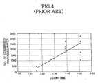
- FIG. 4is a graph illustrating the number of particles of condensed etching gas that form over time on a wafer after the wafer is dry etched.
- the delay time (hours and minutes) in the graphis the amount of time a wafer is exposed to the ambient, e.g., the clean air.
- the delay timeis the time that elapses from the completion of the dry etching of the wafer to the time the FOUP storing the wafer is transferred to the inspection apparatus.
- FIG. 4shows that the number of particles on the wafer increases dramatically after a delay time of about 100 minutes. Therefore, such long delay times allow for the contamination of the wafer to intensify.
- the contaminationis particularly deleterious when the pattern on the wafer is minute, i.e., has a small critical dimension.
- particles of ozonecan facilitate the growth of a natural oxide layer and thereby increasing the resistance of the pattern, and moisture can cause a gate oxide layer to deteriorate.
- condensation phenomenaare most severe for the first wafer which remains within the FOUP for the longest time while at room temperature and under atmospheric pressure.
- the condensation phenomenaalso occur in the conventional dry etching apparatus for etching 200 mm wafers.
- those problemscan be solved by managing the delay time after the wafers are tracked out from the dry etching apparatus up until the time the wafers are subjected to a subsequent cleaning process.
- the first waferexperiences a delay time of about 50 minutes while the FOUP is connected to the substrate transfer module of the dry etching apparatus, i.e., a condensation phenomenon may occur before the wafer is tracked out.
- a processing apparatus for dry etching 300 mm wafersin which the FOUP is directly loaded into a low-vacuum loadlock chamber, has been developed in an attempt to reduce the contamination of the FOUP and the wafers therein.
- the loadlock chamber of this apparatusmust have a large volume to accommodate the relatively large FOUP.
- a great deal of timeis required for forming a vacuum in the loadlock chamber of this apparatus. Accordingly, the efficiency of the apparatus is rather low. Therefore, the above-described apparatus in which the wafers within the FOUP are transferred to the loadlock chamber one-by-one via a substrate transferring module is generally used to process 300 mm wafers.
- An object of the present inventionis to solve the aforementioned problems of the prior art.
- an object of the present inventionis to provide a substrate processing apparatus and method by which the level of contaminants within a substrate transferring module can be controlled.
- Another object of the present inventionis to prevent substrates from being contaminated while they are standing by in a container, such as a FOUP, as other substrates are being processed and subsequently loaded into the FOUP.
- Yet another object of the present inventionis to prevent substrates from being contaminated while they are being transferred in a closed container, such as a FOUP, after being dry etched or the like in a substrate processing apparatus.
- a substrate processing apparatusincludes a container configured to support a plurality of substrates, a substrate processing part including at least one processing chamber in which a predetermined process is performed on the substrate, a substrate transferring module including a substrate transfer chamber through which substrates are transferred to the at least one processing chamber from the container, and a contamination controlling section for controlling the level of contaminants in the chamber of the substrate transfer chamber.
- the substrate transfer modulealso includes a load port disposed outside the substrate transfer chamber and configured to support the container as exposed to the ambient outside the processing apparatus, and substrate transferring means for transferring the substrates from the container.
- the contamination controlling systemincludes a gas inlet port connected to the substrate transfer chamber and through which purging gas is supplied into the substrate transfer chamber, and a gas circulating tube extending outside the substrate transfer chamber and connected to respective portions of said substrate transfer chamber spaced from one another along a length of the chamber. Accordingly, the purging gas in the substrate transfer chamber can be circulated through the substrate transfer chamber using the gas circulating tube.
- a method of processing a substratebegins by providing purging gas into a substrate transfer chamber and circulating the purge gas through the chamber. Then, a container accommodating a plurality of substrates is loaded on a load port outside the substrate transfer chamber. The substrates in the container are transferred into the substrate transfer chamber using a robot disposed in the substrate transfer chamber. From there, the substrates are transferred to at least one processing chamber in which a predetermined process is performed on the substrates. The processed substrates are then transferred into a container. The purging gas is supplied into the substrate transfer chamber and is re-circulated through the chamber from the time the substrates are transferred into the chamber to the time the processed substrates are loaded in the container.
- a purging gassuch as nitrogen gas
- the purging gasis also re-circulated through the substrate transfer chamber to remove moisture and various airborne molecular contaminating materials (AMC) including ozone from the substrate transfer chamber. Therefore, the condensate can be prevented from forming on the processed wafers while they are standing by in a container as more processed wafers are being processed and loaded into the container.
- AMCairborne molecular contaminating materials
- a container supported by the load port of the substrate transferring modulecan be filled with purging gas from the substrate transferring chamber during the loading of substrates into or the unloading of the substrates from the container. In either case, contaminating materials are thus prevented from flowing into the container. In particular, moisture and contaminating materials in the ambient can be prevented from flowing into the container during transferring of the container to another apparatus for performing the next process on the wafers.
- FIG. 1is a plan view of a conventional dry etching apparatus for etching wafers having a diameter of 200 mm;
- FIG. 2is a plan view of a conventional dry etching apparatus for etching wafers having a diameter of 300 mm;
- FIG. 3is a side view of a substrate transfer module of the apparatus illustrated in FIG. 2;
- FIG. 4is a graph illustrating the number of particles that form due to condensation over time on a substrate after the substrate has been dry etched and while the substrate is exposed;
- FIG. 5is a plan view of one embodiment of a substrate processing apparatus according to the present invention.
- FIG. 6is a side view of a substrate transfer module of the substrate processing apparatus illustrated in FIG. 5;
- FIG. 7is a graph illustrating the change of humidity within a substrate transfer chamber and a FOUP over time as the substrate transfer chamber is purged according to the present invention.
- FIG. 8is a side view of another embodiment of a substrate transfer module of a substrate processing apparatus according to the present invention.
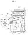
- a dry etching apparatus for etching 300 mm wafersincludes a substrate transferring module 108 , low-vacuum loadlock chambers 122 a and 122 b and a substrate processing section 102 .
- the substrate processing section 102includes a plurality of high-vacuum processing chambers 128 a , 128 b and 128 c , a transferring chamber 124 , and a transferring robot 126 disposed in the transferring chamber 124 .
- Wafers 104 having a diameter of 300 mm, for example,are transferred between the loadlock chambers 122 a and 122 b and the processing chambers 128 a , 128 b and 128 c by the transferring robot 126 .
- Predetermined processessuch as dry etching processes, are carried out on the wafers 104 in the processing chambers 128 a , 128 b and 128 c.
- the substrate transferring module 108includes a substrate transfer chamber 1 - 10 , a substrate transferring apparatus 114 installed in the substrate transfer chamber 110 , at least one load port 112 a and 112 b provided at the exterior of the substrate transferring chamber 110 for supporting a container 106 of wafers 104 , and a filter unit 120 for introducing external air into the substrate transferring chamber 110 .
- the container 106is a FOUP and the substrate transferring apparatus 114 is a robot including a robot arm 116 for supporting the wafers 104 and an arm driving portion 118 for driving the robot arm 116 to transfer the wafers 104 .
- the filter unit 120is a fan filter unit (FFU) in which a fan and a filter are integrated with each other.
- the substrate processing apparatusalso includes a contamination controlling system 130 connected to an outer portion of the substrate transferring module 108 .
- the contamination controlling system 130includes a gas supply inlet 132 for providing the substrate transfer chamber 110 with purging gas 146 a to purge the inside of the substrate transferring chamber 110 , and a gas circulating tube 138 for circulating the purging gas through the substrate transfer chamber 110 .
- the purging gascan be an inert gas or dry air (air from which humidity has been removed).
- the purge gasis nitrogen (N 2 ).
- the contamination controlling system 130also includes a gas line 134 connected to the gas supply inlet 132 , and a mass flow controller (MFC) 136 for controlling the flow rate of the purge gas through the gas line 134 and to the gas supply inlet 132 .
- MFCmass flow controller
- the gas circulating tube 138is extends at one side of the substrate transfer chamber 110 between a lower portion and an uppermost portion of the substrate transfer chamber 110 such that the purging gas recycled back into the substrate transfer chamber 110 through the gas circulating tube 138 forms a laminar flow within the substrate transfer chamber 110 . Also, the gas circulating tube 138 is connected to the fan filter unit 120 so that the purging gas is filtered before it is circulated back into the substrate transfer chamber 110 .
- reference numeral 146 adesignates the purging gas supplied to the substrate transferring chamber 110 through the gas supply inlet 132
- reference numeral 146 bdesignates the purging gas provided back into the substrate transfer chamber 110 through the gas circulating tube 138
- reference numeral 146 cdesignates the purging gas that leaks out naturally from the substrate transferring chamber 110 due to its own pressure.
- the purging gas 146 apreferably nitrogen (N 2 ), is supplied into the substrate transfer chamber 110 through the gas supply inlet 132 to purge the substrate transfer chamber 110 of moisture or other potential contaminants.
- the purging gas within the substrate transferring chamber 110is induced into the gas recycling tube 138 and from there is circulated back into the substrate transferring chamber 110 by the fan filter unit 120 .
- the purging process carried out by the contamination controlling system 130is continuously carried out until the predetermined processes, such as the dry etching of all of the wafers 104 are carried out and the final wafer is transferred into the FOUP 106 .
- a FOUP 106 containing one lot of wafersis loaded on the first load port 112 a of the substrate transferring module 108 .
- the front door 150 a of the FOUP 106 facing the substrate transfer chamber 110 of the substrate transferring module 108is opened.
- a first one of the wafers 104 in the FOUP 106is transferred to the substrate transfer chamber 110 by the substrate transferring apparatus 114 disposed within the substrate transfer chamber 110 .
- a gate valve 152 a between the substrate transfer chamber 110 and the first loadlock chamber 122 ais opened.
- the first waferis loaded into the first loadlock chamber 122 a , in which a low-vacuum state of about 10 ⁇ 3 Torr is maintained, by the substrate transferring apparatus.
- the gate valve 152 a between the substrate transfer chamber 110 and the first loadlock chamber 122 ais then closed and a gate valve 154 a between the transfer chamber 124 of the substrate processing section 102 and the first loadlock chamber 122 a is opened. Then, the first wafer is transferred into the transfer chamber 124 by the transferring robot 126 disposed within the transfer chamber 124 . Next, a gate valve 156 a , 156 b or 156 c between the transfer chamber 124 and a respective processing chamber 128 a , 128 b and 128 c is opened. Then, the first wafer is transferred to the processing respective chamber 128 a , 128 b and 128 c by the transferring robot 126 . At this time, the processing chambers 128 a , 128 b and 128 c are maintained at a high-vacuum state of about 10 ⁇ 6 Torr.
- the gate valve 156 a , 156 b or 156 cis then closed, and the first wafer is subjected to a predetermined process, such as a dry etching process, within the processing chamber 128 a , 128 b or 128 c.
- the gate valve 156 a , 156 b or 156 c between the transfer chamber 124 and the respective processing chamber 128 a , 128 b or 128 cis opened after the first wafer is processed therein.
- the first waferis then transferred into the transfer chamber 124 using the transferring robot 126 .
- the gate valve 156 a , 156 b or 156 c between the transfer chamber 124 and the processing chambers 128 a , 128 b or 128 cis closed. Then a gate valve 154 b between the transfer chamber 124 and the second loadlock chamber 122 b is opened. Then, the first wafer is transferred to the second loadlock chamber using the transferring robot 126 .
- the gate valve 154 b between the transfer chamber 124 and the second loadlock chamber 122 ais closed, and the gate valve 152 b between the substrate transfer chamber 110 and the second loadlock chamber 122 b is opened.
- the first waferis transferred into the substrate transfer chamber 110 by the substrate transferring apparatus 114 .
- the substrate transferring apparatus 114is transfers the first wafer from the substrate transfer chamber 110 into the FOUP 106 on the second load port 112 b .
- the first waferstands ready in the FOUP 106 for about 50 minutes until the remaining wafers are processed and transferred into the FOUP 106 .
- the interior of the substrate transfer chamber 110 connected to the FOUP 106is continuously purged by nitrogen gas during this time so that moisture and contaminants are removed from the substrate transfer chamber 110 . Therefore, the purging process prevents the first wafer from absorbing humidity and other potential contaminants.
- the front door of the FOUPis closed and the no more purging gas is supplied into the substrate transferring chamber 110 once all the processed wafers are received in the FOUP 106 . Then, the FOUP 106 is removed from the dry etching apparatus.
- the front doors 150 a and 150 b of the FOUPs 106are opened while the FOUPs 106 are supported by the load ports 112 a and 112 b during the processing of the wafers 104 . Therefore, the purging gas, such as nitrogen (N 2 ), supplied into the substrate transfer chamber 110 fills the FOUPs 106 . Accordingly, the purging filling the FOUP 106 prevents an inflow of humidity and airborne molecular contaminating material (AMC) when the FOUP 106 is subsequently transferred to another apparatus. In the case of the FOUP containing the processed wafers, the wafers are prevented from absorbing humidity and airborne molecular contaminating material (AMC) prior to the next process.
- AMCairborne molecular contaminating material
- FIG. 7is a graph illustrating a change in the humidity within the substrate transferring chamber and a FOUP as the substrate transfer chamber is purged by nitrogen gas.
- Region ⁇ circle over ( 1 ) ⁇ in the graphcorresponds to the interval over which the purging gas is initially introduced into the substrate transferring chamber.
- Region ⁇ circle over ( 2 ) ⁇corresponds to the interval during which FOUP is provided on a load port outside the substrate transfer chamber.
- Region ⁇ circle over ( 3 ) ⁇corresponds to the interval during which the FOUP is removed from the load port.
- Plot Aindicates the relative humidity in the substrate transfer chamber and plot B indicates the relative humidity in the FOUP.
- the humidity in the substrate transfer chamberis reduced from about 25% to about 4% during the time the nitrogen (N 2 ) gas is supplied into the substrate transfer chamber. Also, the nitrogen gas fills the FOUP while the wafers are being processed during this time because the front door of the FOUP remains open. Accordingly, the humidity in the FOUP is decreased from about 30% to about 6%.
- FIG. 8is a side view of a second embodiment of a substrate transferring module 108 ′ of a substrate processing apparatus according to the present invention.
- the second embodiment of the substrate transferring module 108 ′is the same as that 108 of the first embodiment except for the contamination controlling system. Accordingly, only the contamination controlling system will be described for the sake of brevity.
- the contamination controlling system 130includes a gas supply inlet 132 for providing purging gas 146 a (an inert gas such as nitrogen (N 2 ) or a dried gas) into the substrate transfer chamber 110 , a gas supply line 134 , an MFC 136 associated with the gas supply line 134 , and a gas circulating tube 138 for circulating the purging gas through the substrate transfer chamber 110 .
- purging gas 146 aan inert gas such as nitrogen (N 2 ) or a dried gas
- the contamination controlling system 130 of this embodimentalso includes a sensor 140 for detecting the temperature or humidity inside the substrate transfer chamber 110 , a controller 144 (CNR) for controlling the MFC 136 to regulate the amount of purging gas 146 a supplied into the substrate transfer chamber 110 , and a data receiving portion 142 (DRP) for recording the temperature and humidity detected by the sensor 140 and transmitting this data to the controller 144 (CNR).
- CNRcontroller 144
- DSPdata receiving portion 142
- the moisture or other contaminating material in the substrate transferring chamber 110is purged by supplying the purging gas 146 a into the substrate transfer chamber 110 through the gas supply inlet 132 of the contamination controlling system 130 .
- the purging gas in the substrate transferring chamber 110is induced into the gas circulating tube 138 and is thus supplied back into the substrate transfer chamber 110 .
- the temperature and humidity in the substrate transfer chamber 110is measured in real time by the sensor 140 while the purging gas 146 a is supplied into the substrate transfer chamber 110 .
- the measurementsare transmitted to the controller 144 by the data receiving portion 142 .
- the controller 144then controls the operation of the MFC 136 based on the data received from the data receiving portion 142 .
- an operatormay set an allowable value of less than 1% for the humidity (a moisture concentration in a range of about 1000 to about 500 ppm).
- the controller 144controls the MFC 136 so as to increase the amount of purging gas supplied into the substrate transferring chamber 110 .
- the controller 144controls the MFC 136 to decrease the amount of the purging gas being supplied into the substrate transferring chamber 110 when the measured moisture concentration is lower than the allowable value set by the operator.
- purging gasis supplied into and circulated throughout the substrate transfer chamber of a substrate transferring module for transferring substrates from a container to a substrate processing section in which the substrates are processed. Accordingly, the humidity and the amount of airborne molecular contaminating material (AMC) including ozone are controlled in the substrate transferring chamber. Therefore, the formation of particles by condensation on the wafers can be prevented while the wafers standby in the container after being processed.
- AMCairborne molecular contaminating material
- the container supported on the load port of the substrate transferring moduleis filled with the purging gas. Accordingly, an inflow of moisture and external contaminating material into the container is prevented while the container is being transferred with the processed wafers to another apparatus. Therefore, the wafers are also prevented from being contaminated between processes.
- the humidity in the substrate transfer chambercan be automatically controlled to a desired concentration by monitoring the temperature and humidity in the substrate transfer chamber in real time and by controlling the amount of purging gas supplied into the substrate transfer chamber. Accordingly, this further enhances the ability to prevent the wafers from being contaminated inside the container used to transfer the wafers.
Landscapes
- Engineering & Computer Science (AREA)
- Physics & Mathematics (AREA)
- Condensed Matter Physics & Semiconductors (AREA)
- General Physics & Mathematics (AREA)
- Manufacturing & Machinery (AREA)
- Computer Hardware Design (AREA)
- Microelectronics & Electronic Packaging (AREA)
- Power Engineering (AREA)
- Container, Conveyance, Adherence, Positioning, Of Wafer (AREA)
Abstract
Description
- 1. Field of the Invention[0001]
- The present invention relates to a substrate processing apparatus and to a method of transferring the substrate to a processing chamber of the apparatus. More particularly, the present invention relates to a substrate transfer module for transferring a substrate from a container to a substrate processing chamber.[0002]
- 2. Description of the Related Art[0003]
- The manufacturing of semiconductor devices generally includes a photolithographic process in which a photoresist pattern is formed on a wafer, and a dry etching process in which the wafer is subsequently etched using the photoresist pattern as an etching mask. The dry etching process is performed in a processing, chamber under a high vacuum state. However, a considerable amount of time is required for creating the high vacuum state in the processing chamber, i.e., for reducing the pressure from atmospheric pressure to a high vacuum pressure. Therefore, a low-vacuum loadlock chamber is used as a buffer in a dry etching apparatus so that wafers may stand ready while the high vacuum pressure is being created in the process chamber, whereby the wafers may be processed efficiently.[0004]
- FIG. 1 is a plan view of a conventional multi-chamber dry etching apparatus for wafers having a diameter of 200 mm. Referring to FIG. 1, the conventional dry etching apparatus includes low-[0005]
vacuum loadlock chambers transfer chamber 15, and high-vacuum processing chambers - A[0006]
cassette 12 that accommodates about 25 wafers, that is,semiconductor substrates 20, is loaded into theloadlock chamber 14a. A low-vacuum state of about 10−3Torr is maintained in theloadlock chamber 14a. Thereafter, thewafers 20 in thefirst loadlock chamber 14aare transferred one-by-one torespective processing chambers robot 16 disposed in thetransfer chamber 15. All of theprocessing chambers wafers 20 are also transferred by therobot 16 to thesecond loadlock chamber 14bafter the dry etching process is completed within theprocessing chambers wafer cassette 12 in thesecond loadlock chamber 14bremoved from the dry etching apparatus once all of theetched wafers 20 are received in thecassette 12. - Meanwhile, larger wafers are now being used to improve the efficiency of the overall semiconductor device manufacturing process and to save manufacturing costs. In particular, semiconductor wafers having a diameter of 300 mm are now being used to manufacture semiconductor devices. Accordingly, the semiconductor manufacturing apparatus and processes have been developed in line with the increase in the size of the wafers being used.[0007]
- For instance, wafers having a diameter of 300 mm are stored and transported within a wafer container such as a front opening unified pod (FOUP). The FOUP is has a relatively large volume. Therefore, when the FOUP is introduced into the low-vacuum loadlock chamber, a large amount of time is required to reduce the pressure in the loadlock chamber from atmospheric pressure to a low vacuum pressure. Likewise, a large amount of time is required to subsequently increase the pressure in the loadlock chamber from the low vacuum pressure to atmospheric pressure. Therefore, the efficiency of the dry etching process using this type of apparatus is relatively low.[0008]
- More specifically, apparatus for processing 300 mm wafers include a separately formed substrate transferring module, such as an equipment front end module (EFEM). The FOUP is loaded on a load port of the substrate transferring module and the wafers are transferred one-by-one to the loadlock chamber via the substrate transferring module.[0009]
- FIGS. 2 and 3 show a conventional multi-chamber dry etching apparatus for dry etching 300 mm wafers. Referring to FIG. 2, the conventional dry etching apparatus includes a[0010]
substrate transferring module 50, low-vacuum loadlock chambers substrate processing section 65. Thesubstrate processing section 65 has a plurality of high-vacuum processing chambers wafers 62, and atransfer chamber 63 through which thewafers 62 are transferred between theloadlock chambers processing chambers - As shown in FIG. 3, the[0011]
substrate transferring module 50 includesload ports filter unit 59 for filtering air from the outside, and asubstrate transfer chamber 54 in which asubstrate transferring robot 56 is installed. Referring to FIGS. 2 and 3, the FOUP52 accommodates one lot of wafers, e.g., 25wafers 62. The FOUP52 is placed on thefirst load port 58aof thesubstrate transferring module 50. Then, a front door (not shown) of the FOUP52 facing thesubstrate transfer chamber 54 is opened. - The[0012]
filter unit 59 of thesubstrate transferring module 50 is a fan filter unit (FFU) in which a fan and a filter are combined. Thefilter unit 59 allows theclean air 80 from aclean room filter 75 to flow down into thesubstrate transferring chamber 54. Accordingly, thesubstrate transferring chamber 54 has the same temperature and atmospheric pressure (temperature of about 23° C., humidity of about 45%) as theclean air 80 flowing from thefilter unit 59. Since the FOUP52 is connected to thesubstrate transfer chamber 54 while the front door of the FOUP52 is opened, theclean air 80 flows from thesubstrate transfer chamber 54 into the FOUP52. Hence, the interior of the FOUP is at the same temperature (room) and pressure (atmospheric) as the air in thesubstrate transfer chamber 54. - A first wafer one of the[0013]
wafers 62 is loaded into thefirst loadlock chamber 60ain which a low-vacuum state of about 10−3Torr is maintained, using thesubstrate transferring robot 56 disposed within thesubstrate transfer chamber 54. Then, thewafer 62 in thefirst loadlock chamber 60ais transferred to arespective processing chambers robot 64 disposed within thetransfer chamber 63. A high vacuum pressure of about 10−6Torr is maintained in all theprocessing chambers - Once the[0014]
first wafer 62 is dry etched, the wafer is transferred to thesecond loadlock chamber 60busing the transferringrobot 64. After that, thefirst wafer 62 is transferred to a FOUP52 disposed on thesecond load port 58busing thesubstrate transferring robot 56. The wafer remains there in the FOUP52 for about 50 minutes until the remaining wafers are processed. When all the wafers of the other wafers are processed and received in theFOUP 52, the front door of the FOUP52 is closed and the FOUP52 is removed from the dry etching apparatus. - As described above, in the conventional dry etching apparatus for dry etching 200 mm wafers, a wafer cassette accommodating[0015]25 wafers is directly loaded into the low-vacuum loadlock chamber so that the cassette is isolated from the external clean air. On the contrary, in the conventional dry etching apparatus for etching 300 mm wafers, the wafers are transferred to the
first loadlock chamber 60aone-by-one from the FOUP52 using thesubstrate transferring module 50. That is, the FOUP containing thewafers 62 remains on thesecond load port 58bof thesubstrate transferring module 50 while the front door of the FOUP52 is opened and exposed to theclean air 80. Thus, the processing of the 300 mm wafers requires a great deal of time. - The characteristics of the conventional dry etching apparatus for etching 200 mm wafers and the conventional dry etching apparatus for etching 300 mm wafers are set out in the following Table 1.[0016]
TABLE 1 1 2 3 4 5 6 7 8 9 200 clean Cassette in transfer processing transfer cassette in clean mm room loadlock chamber chamber chamber loadlock room chamber chamber 25 wafers by 1 by 1 by 1 25 wafers 1 10−3 10−6 10−6 10−6 10−3 1 atm Torr Torr Torr Torr Torr atm 300 FOUP EFEM load- transfer processing transfer loadlock EFEM FOUP mm lock chamber chamber chamber 25 by 1 By 1 by 1 by 1 by 1 by 1 by 1 25 wafers wafers 1 1 10−3 10−6 10−6 10−6 10−3 1 1 atm atm Torr Torr Torr Torr Torr atm atm - As shown in Table 1, in the conventional dry etching apparatus for etching 300 mm wafers, the wafers are under room temperature and under an atmospheric pressure as they are transferred one-by-one between the loadlock chamber and a FOUP connected to the substrate transferring module (EFEM). Therefore, a great deal of time elapses while the etched wafers remain in the FOUP while the front door of the FOUP is open.[0017]
- During this time, these wafers standing by in the FOUP are exposed to the clean air via the substrate transferring module. Accordingly, the wafers in the FOUP are exposed to various airborne molecular contamination (AMC) such as moisture (H[0018]2O) and ozone (O3) in the clean air. In this case, etching gas remaining on the surface of the wafer and the moisture in the air react, i.e., the etching gas condenses. The condensed etching gas forms minute particles that may bridge adjacent conductive patterns on the wafer.
- FIG. 4 is a graph illustrating the number of particles of condensed etching gas that form over time on a wafer after the wafer is dry etched. The delay time (hours and minutes) in the graph is the amount of time a wafer is exposed to the ambient, e.g., the clean air. In the graph of FIG. 4, the delay time is the time that elapses from the completion of the dry etching of the wafer to the time the FOUP storing the wafer is transferred to the inspection apparatus. FIG. 4 shows that the number of particles on the wafer increases dramatically after a delay time of about 100 minutes. Therefore, such long delay times allow for the contamination of the wafer to intensify. Moreover, the contamination is particularly deleterious when the pattern on the wafer is minute, i.e., has a small critical dimension. For instance, particles of ozone can facilitate the growth of a natural oxide layer and thereby increasing the resistance of the pattern, and moisture can cause a gate oxide layer to deteriorate.[0019]
- These ‘condensation phenomena’ are most severe for the first wafer which remains within the FOUP for the longest time while at room temperature and under atmospheric pressure. The condensation phenomena also occur in the conventional dry etching apparatus for etching 200 mm wafers. However, those problems can be solved by managing the delay time after the wafers are tracked out from the dry etching apparatus up until the time the wafers are subjected to a subsequent cleaning process. In the conventional dry etching apparatus for etching 300 mm wafers, the first wafer experiences a delay time of about 50 minutes while the FOUP is connected to the substrate transfer module of the dry etching apparatus, i.e., a condensation phenomenon may occur before the wafer is tracked out.[0020]
- A processing apparatus for dry etching 300 mm wafers, in which the FOUP is directly loaded into a low-vacuum loadlock chamber, has been developed in an attempt to reduce the contamination of the FOUP and the wafers therein. However, the loadlock chamber of this apparatus must have a large volume to accommodate the relatively large FOUP. Hence, a great deal of time is required for forming a vacuum in the loadlock chamber of this apparatus. Accordingly, the efficiency of the apparatus is rather low. Therefore, the above-described apparatus in which the wafers within the FOUP are transferred to the loadlock chamber one-by-one via a substrate transferring module is generally used to process 300 mm wafers.[0021]
- An object of the present invention is to solve the aforementioned problems of the prior art.[0022]
- More specifically, an object of the present invention is to provide a substrate processing apparatus and method by which the level of contaminants within a substrate transferring module can be controlled.[0023]
- Another object of the present invention is to prevent substrates from being contaminated while they are standing by in a container, such as a FOUP, as other substrates are being processed and subsequently loaded into the FOUP.[0024]
- Yet another object of the present invention is to prevent substrates from being contaminated while they are being transferred in a closed container, such as a FOUP, after being dry etched or the like in a substrate processing apparatus.[0025]
- In accordance with one aspect of the present invention, a substrate processing apparatus includes a container configured to support a plurality of substrates, a substrate processing part including at least one processing chamber in which a predetermined process is performed on the substrate, a substrate transferring module including a substrate transfer chamber through which substrates are transferred to the at least one processing chamber from the container, and a contamination controlling section for controlling the level of contaminants in the chamber of the substrate transfer chamber.[0026]
- The substrate transfer module also includes a load port disposed outside the substrate transfer chamber and configured to support the container as exposed to the ambient outside the processing apparatus, and substrate transferring means for transferring the substrates from the container. The contamination controlling system includes a gas inlet port connected to the substrate transfer chamber and through which purging gas is supplied into the substrate transfer chamber, and a gas circulating tube extending outside the substrate transfer chamber and connected to respective portions of said substrate transfer chamber spaced from one another along a length of the chamber. Accordingly, the purging gas in the substrate transfer chamber can be circulated through the substrate transfer chamber using the gas circulating tube.[0027]
- In accordance with another aspect of the present invention, a method of processing a substrate begins by providing purging gas into a substrate transfer chamber and circulating the purge gas through the chamber. Then, a container accommodating a plurality of substrates is loaded on a load port outside the substrate transfer chamber. The substrates in the container are transferred into the substrate transfer chamber using a robot disposed in the substrate transfer chamber. From there, the substrates are transferred to at least one processing chamber in which a predetermined process is performed on the substrates. The processed substrates are then transferred into a container. The purging gas is supplied into the substrate transfer chamber and is re-circulated through the chamber from the time the substrates are transferred into the chamber to the time the processed substrates are loaded in the container.[0028]
- According to the present invention, a purging gas, such as nitrogen gas, is supplied to the substrate transfer chamber of the substrate transferring module for transferring substrates from a container to one or more substrate processing chambers. The purging gas is also re-circulated through the substrate transfer chamber to remove moisture and various airborne molecular contaminating materials (AMC) including ozone from the substrate transfer chamber. Therefore, the condensate can be prevented from forming on the processed wafers while they are standing by in a container as more processed wafers are being processed and loaded into the container.[0029]
- Also, a container supported by the load port of the substrate transferring module can be filled with purging gas from the substrate transferring chamber during the loading of substrates into or the unloading of the substrates from the container. In either case, contaminating materials are thus prevented from flowing into the container. In particular, moisture and contaminating materials in the ambient can be prevented from flowing into the container during transferring of the container to another apparatus for performing the next process on the wafers.[0030]
- The above objects and advantages of the present invention will become readily apparent by reference to the following detailed description made in conjunction with the accompanying drawings wherein:[0031]
- FIG. 1 is a plan view of a conventional dry etching apparatus for etching wafers having a diameter of 200 mm;[0032]
- FIG. 2 is a plan view of a conventional dry etching apparatus for etching wafers having a diameter of 300 mm;[0033]
- FIG. 3 is a side view of a substrate transfer module of the apparatus illustrated in FIG. 2;[0034]
- FIG. 4 is a graph illustrating the number of particles that form due to condensation over time on a substrate after the substrate has been dry etched and while the substrate is exposed;[0035]
- FIG. 5 is a plan view of one embodiment of a substrate processing apparatus according to the present invention;[0036]
- FIG. 6 is a side view of a substrate transfer module of the substrate processing apparatus illustrated in FIG. 5;[0037]
- FIG. 7 is a graph illustrating the change of humidity within a substrate transfer chamber and a FOUP over time as the substrate transfer chamber is purged according to the present invention; and[0038]
- FIG. 8 is a side view of another embodiment of a substrate transfer module of a substrate processing apparatus according to the present invention.[0039]
- Hereinafter, the preferred embodiments of the present invention will be described in detail with reference to the attached drawings. The same reference numeral designate like parts throughout the drawings.[0040]
- Referring first to FIG. 5, a dry etching apparatus for etching 300 mm wafers includes a[0041]
substrate transferring module 108, low-vacuum loadlock chambers substrate processing section 102. - The[0042]
substrate processing section 102 includes a plurality of high-vacuum processing chambers chamber 124, and a transferringrobot 126 disposed in the transferringchamber 124.Wafers 104 having a diameter of 300 mm, for example, are transferred between theloadlock chambers processing chambers robot 126. Predetermined processes, such as dry etching processes, are carried out on thewafers 104 in theprocessing chambers - Referring now to both FIGS. 5 and 6, the[0043]
substrate transferring module 108 includes a substrate transfer chamber1-10, asubstrate transferring apparatus 114 installed in thesubstrate transfer chamber 110, at least oneload port substrate transferring chamber 110 for supporting acontainer 106 ofwafers 104, and afilter unit 120 for introducing external air into thesubstrate transferring chamber 110. - Preferably, the[0044]
container 106 is a FOUP and thesubstrate transferring apparatus 114 is a robot including arobot arm 116 for supporting thewafers 104 and anarm driving portion 118 for driving therobot arm 116 to transfer thewafers 104. Thefilter unit 120 is a fan filter unit (FFU) in which a fan and a filter are integrated with each other. - The substrate processing apparatus also includes a[0045]
contamination controlling system 130 connected to an outer portion of thesubstrate transferring module 108. Thecontamination controlling system 130 includes agas supply inlet 132 for providing thesubstrate transfer chamber 110 with purginggas 146ato purge the inside of thesubstrate transferring chamber 110, and agas circulating tube 138 for circulating the purging gas through thesubstrate transfer chamber 110. The purging gas can be an inert gas or dry air (air from which humidity has been removed). Preferably, the purge gas is nitrogen (N2). Thecontamination controlling system 130 also includes agas line 134 connected to thegas supply inlet 132, and a mass flow controller (MFC)136 for controlling the flow rate of the purge gas through thegas line 134 and to thegas supply inlet 132. - The[0046]
gas circulating tube 138 is extends at one side of thesubstrate transfer chamber 110 between a lower portion and an uppermost portion of thesubstrate transfer chamber 110 such that the purging gas recycled back into thesubstrate transfer chamber 110 through thegas circulating tube 138 forms a laminar flow within thesubstrate transfer chamber 110. Also, thegas circulating tube 138 is connected to thefan filter unit 120 so that the purging gas is filtered before it is circulated back into thesubstrate transfer chamber 110. - Now, when the ambient within the[0047]
substrate transfer chamber 110 are purged by the purging gas, the process would consume a large amount of purging gas and pose problems relating to the exhausting of the purging gas. Therefore, it is preferred that only a portion of the total volume of the ambient in thesubstrate transfer chamber 110 be purged utilizing the purging gas, and that the purging gas recycled back into thesubstrate transfer chamber 110 be exhausted through a natural leakage of the purging. In FIG. 6,reference numeral 146adesignates the purging gas supplied to thesubstrate transferring chamber 110 through thegas supply inlet 132,reference numeral 146bdesignates the purging gas provided back into thesubstrate transfer chamber 110 through thegas circulating tube 138, andreference numeral 146cdesignates the purging gas that leaks out naturally from thesubstrate transferring chamber 110 due to its own pressure. - The operation of the above-described substrate processing apparatus will now be described in more detail.[0048]
- First, clean air is introduced into the[0049]
substrate transfer chamber 110 through thefan filter unit 120 before a predetermined process, such as a dry etching process, is carried out Therefore, the interior of thesubstrate transferring chamber 110 is maintained at the same temperature and humidity as the clean air outside thechamber 110, for example, at a temperature of about 23° C. and at a humidity of about 45%. - Next, the purging[0050]
gas 146a, preferably nitrogen (N2), is supplied into thesubstrate transfer chamber 110 through thegas supply inlet 132 to purge thesubstrate transfer chamber 110 of moisture or other potential contaminants. The purging gas within thesubstrate transferring chamber 110 is induced into thegas recycling tube 138 and from there is circulated back into thesubstrate transferring chamber 110 by thefan filter unit 120. The purging process carried out by thecontamination controlling system 130 is continuously carried out until the predetermined processes, such as the dry etching of all of thewafers 104 are carried out and the final wafer is transferred into theFOUP 106. - During the purging process, a[0051]
FOUP 106 containing one lot of wafers, that is, twenty-fivewafers 104, is loaded on thefirst load port 112aof thesubstrate transferring module 108. Subsequently, thefront door 150aof theFOUP 106 facing thesubstrate transfer chamber 110 of thesubstrate transferring module 108 is opened. A first one of thewafers 104 in theFOUP 106 is transferred to thesubstrate transfer chamber 110 by thesubstrate transferring apparatus 114 disposed within thesubstrate transfer chamber 110. Then, agate valve 152abetween thesubstrate transfer chamber 110 and thefirst loadlock chamber 122ais opened. The first wafer is loaded into thefirst loadlock chamber 122a, in which a low-vacuum state of about 10−3Torr is maintained, by the substrate transferring apparatus. - The[0052]
gate valve 152abetween thesubstrate transfer chamber 110 and thefirst loadlock chamber 122ais then closed and agate valve 154abetween thetransfer chamber 124 of thesubstrate processing section 102 and thefirst loadlock chamber 122ais opened. Then, the first wafer is transferred into thetransfer chamber 124 by the transferringrobot 126 disposed within thetransfer chamber 124. Next, agate valve transfer chamber 124 and arespective processing chamber respective chamber robot 126. At this time, theprocessing chambers - The[0053]
gate valve processing chamber - The[0054]
gate valve transfer chamber 124 and therespective processing chamber transfer chamber 124 using the transferringrobot 126. - The[0055]
gate valve transfer chamber 124 and theprocessing chambers gate valve 154bbetween thetransfer chamber 124 and thesecond loadlock chamber 122bis opened. Then, the first wafer is transferred to the second loadlock chamber using the transferringrobot 126. - Next, the[0056]
gate valve 154bbetween thetransfer chamber 124 and thesecond loadlock chamber 122ais closed, and thegate valve 152bbetween thesubstrate transfer chamber 110 and thesecond loadlock chamber 122bis opened. Then, the first wafer is transferred into thesubstrate transfer chamber 110 by thesubstrate transferring apparatus 114. Subsequently, thesubstrate transferring apparatus 114 is transfers the first wafer from thesubstrate transfer chamber 110 into theFOUP 106 on thesecond load port 112b. The first wafer stands ready in theFOUP 106 for about 50 minutes until the remaining wafers are processed and transferred into theFOUP 106. However, the interior of thesubstrate transfer chamber 110 connected to theFOUP 106 is continuously purged by nitrogen gas during this time so that moisture and contaminants are removed from thesubstrate transfer chamber 110. Therefore, the purging process prevents the first wafer from absorbing humidity and other potential contaminants. The front door of the FOUP is closed and the no more purging gas is supplied into thesubstrate transferring chamber 110 once all the processed wafers are received in theFOUP 106. Then, theFOUP 106 is removed from the dry etching apparatus. - According to the present invention, as described above, the[0057]
front doors FOUPs 106 are opened while theFOUPs 106 are supported by theload ports wafers 104. Therefore, the purging gas, such as nitrogen (N2), supplied into thesubstrate transfer chamber 110 fills theFOUPs 106. Accordingly, the purging filling theFOUP 106 prevents an inflow of humidity and airborne molecular contaminating material (AMC) when theFOUP 106 is subsequently transferred to another apparatus. In the case of the FOUP containing the processed wafers, the wafers are prevented from absorbing humidity and airborne molecular contaminating material (AMC) prior to the next process. - FIG. 7 is a graph illustrating a change in the humidity within the substrate transferring chamber and a FOUP as the substrate transfer chamber is purged by nitrogen gas. Region {circle over ([0058]1)} in the graph corresponds to the interval over which the purging gas is initially introduced into the substrate transferring chamber. Region {circle over (2)} corresponds to the interval during which FOUP is provided on a load port outside the substrate transfer chamber. Region {circle over (3)} corresponds to the interval during which the FOUP is removed from the load port. Plot A indicates the relative humidity in the substrate transfer chamber and plot B indicates the relative humidity in the FOUP.
- Referring to FIG. 7, the humidity in the substrate transfer chamber is reduced from about 25% to about 4% during the time the nitrogen (N[0059]2) gas is supplied into the substrate transfer chamber. Also, the nitrogen gas fills the FOUP while the wafers are being processed during this time because the front door of the FOUP remains open. Accordingly, the humidity in the FOUP is decreased from about 30% to about 6%.
- After the front door of the FOUP was closed and the FOUP was unloaded from the load port, the FOUP was placed in a clean room. Here, it took about one hour and ten minutes for the humidity within the FOUP to increase to about 50% of that of the humidity of the air in the clean room outside the FOUP. Accordingly, an inflow of humidity and airborne molecular contaminating material (AMC) into the FOUP can be prevented during the time the FOUP remains in a clean room between processes, i.e., between the time the door of the FOUP is closed and the FOUP is transferred to another apparatus.[0060]
- FIG. 8 is a side view of a second embodiment of a[0061]
substrate transferring module 108′ of a substrate processing apparatus according to the present invention. The second embodiment of thesubstrate transferring module 108′ is the same as that108 of the first embodiment except for the contamination controlling system. Accordingly, only the contamination controlling system will be described for the sake of brevity. - As in the first embodiment, the[0062]
contamination controlling system 130 includes agas supply inlet 132 for providing purginggas 146a(an inert gas such as nitrogen (N2) or a dried gas) into thesubstrate transfer chamber 110, agas supply line 134, anMFC 136 associated with thegas supply line 134, and agas circulating tube 138 for circulating the purging gas through thesubstrate transfer chamber 110. - However, the[0063]
contamination controlling system 130 of this embodiment also includes asensor 140 for detecting the temperature or humidity inside thesubstrate transfer chamber 110, a controller144 (CNR) for controlling theMFC 136 to regulate the amount of purginggas 146asupplied into thesubstrate transfer chamber 110, and a data receiving portion142 (DRP) for recording the temperature and humidity detected by thesensor 140 and transmitting this data to the controller144 (CNR). - Once again, the moisture or other contaminating material in the[0064]
substrate transferring chamber 110 is purged by supplying the purginggas 146ainto thesubstrate transfer chamber 110 through thegas supply inlet 132 of thecontamination controlling system 130. During this time, the purging gas in thesubstrate transferring chamber 110 is induced into thegas circulating tube 138 and is thus supplied back into thesubstrate transfer chamber 110. - In addition, the temperature and humidity in the[0065]
substrate transfer chamber 110 is measured in real time by thesensor 140 while the purginggas 146ais supplied into thesubstrate transfer chamber 110. The measurements are transmitted to thecontroller 144 by thedata receiving portion 142. Thecontroller 144 then controls the operation of theMFC 136 based on the data received from thedata receiving portion 142. - For example, an operator may set an allowable value of less than 1% for the humidity (a moisture concentration in a range of about 1000 to about 500 ppm). In this case, if the measured moisture concentration in the[0066]
substrate transferring chamber 110 exceeds the allowable value, thecontroller 144 controls theMFC 136 so as to increase the amount of purging gas supplied into thesubstrate transferring chamber 110. On the contrary, thecontroller 144 controls theMFC 136 to decrease the amount of the purging gas being supplied into thesubstrate transferring chamber 110 when the measured moisture concentration is lower than the allowable value set by the operator. - As described above, according to the present invention, purging gas is supplied into and circulated throughout the substrate transfer chamber of a substrate transferring module for transferring substrates from a container to a substrate processing section in which the substrates are processed. Accordingly, the humidity and the amount of airborne molecular contaminating material (AMC) including ozone are controlled in the substrate transferring chamber. Therefore, the formation of particles by condensation on the wafers can be prevented while the wafers standby in the container after being processed.[0067]
- In addition, the container supported on the load port of the substrate transferring module is filled with the purging gas. Accordingly, an inflow of moisture and external contaminating material into the container is prevented while the container is being transferred with the processed wafers to another apparatus. Therefore, the wafers are also prevented from being contaminated between processes.[0068]
- Furthermore, the humidity in the substrate transfer chamber can be automatically controlled to a desired concentration by monitoring the temperature and humidity in the substrate transfer chamber in real time and by controlling the amount of purging gas supplied into the substrate transfer chamber. Accordingly, this further enhances the ability to prevent the wafers from being contaminated inside the container used to transfer the wafers.[0069]
- Finally, although the preferred embodiments of the present invention have been described, it is understood that the present invention should not be limited to these preferred embodiments but various changes and modifications can be made by one skilled in the art within the true spirit and scope of the present invention as hereinafter claimed.[0070]
Claims (20)
Applications Claiming Priority (2)
| Application Number | Priority Date | Filing Date | Title |
|---|---|---|---|
| KR10-2002-0075458AKR100486690B1 (en) | 2002-11-29 | 2002-11-29 | Substrate processing apparatus and method for controlling contamination in substrate transfer module |
| KR2002-75458 | 2002-11-29 |
Publications (2)
| Publication Number | Publication Date |
|---|---|
| US20040105738A1true US20040105738A1 (en) | 2004-06-03 |
| US6996453B2 US6996453B2 (en) | 2006-02-07 |
Family
ID=32388283
Family Applications (1)
| Application Number | Title | Priority Date | Filing Date |
|---|---|---|---|
| US10/684,436Expired - Fee RelatedUS6996453B2 (en) | 2002-11-29 | 2003-10-15 | Substrate processing apparatus and method of processing substrate while controlling for contamination in substrate transfer module |
Country Status (5)
| Country | Link |
|---|---|
| US (1) | US6996453B2 (en) |
| JP (1) | JP4553574B2 (en) |
| KR (1) | KR100486690B1 (en) |
| DE (1) | DE10353326B4 (en) |
| TW (1) | TWI251258B (en) |
Cited By (351)
| Publication number | Priority date | Publication date | Assignee | Title |
|---|---|---|---|---|
| US20050135905A1 (en)* | 2003-12-04 | 2005-06-23 | Daifuku Co., Ltd. | Glass substrate transporting facility |
| US7096752B1 (en)* | 2004-11-02 | 2006-08-29 | Kla-Tencor Technologies Corporation | Environmental damage reduction |
| US20060263197A1 (en)* | 2005-05-18 | 2006-11-23 | International Business Machines Corporation | Pod swapping internal to tool run time |
| US20070107598A1 (en)* | 2005-11-14 | 2007-05-17 | Jin-Goo Lee | Load-lock and semiconductor device manufacturing equipment comprising the same |
| US20080023442A1 (en)* | 2006-07-20 | 2008-01-31 | Shoko Ito | Method for manufacturing electronic device |
| US20080050924A1 (en)* | 2006-08-23 | 2008-02-28 | Tokyo Electron Limited | Substrate carrying apparatus and substrate carrying method |
| US20100184296A1 (en)* | 2009-01-16 | 2010-07-22 | Nec Electronics Corporation | Semiconductor device manufacturing method, wafer treatment system, and recording medium |
| US20110174337A1 (en)* | 2010-01-20 | 2011-07-21 | Tokyo Electron Limited | Method and apparatus for recovering pattern on silicon substrate |
| CN102751392A (en)* | 2011-04-19 | 2012-10-24 | 北京北方微电子基地设备工艺研究中心有限责任公司 | Chip process device and chip process method |
| US9136149B2 (en) | 2012-11-16 | 2015-09-15 | Taiwan Semiconductor Manufacturing Company, Ltd. | Loading port, system for etching and cleaning wafers and method of use |
| CN105556652A (en)* | 2013-07-08 | 2016-05-04 | 布鲁克斯自动化公司 | Process apparatus with on-the-fly substrate centering |
| US9704727B2 (en) | 2013-12-13 | 2017-07-11 | Sinfonia Technology Co., Ltd. | Efem |
| EP3264451A4 (en)* | 2015-02-27 | 2018-10-24 | Sinfonia Technology Co., Ltd. | Transfer chamber |
| US20180366355A1 (en)* | 2013-08-12 | 2018-12-20 | Applied Materials, Inc. | Substrate processing systems, apparatus, and methods with factory interface environmental controls |
| EP3376529A4 (en)* | 2015-11-10 | 2019-07-03 | Sinfonia Technology Co., Ltd. | ROBOTIC TRANSPORT DEVICE |
| US10347510B2 (en) | 2015-07-23 | 2019-07-09 | Tokyo Electron Limited | Substrate transfer chamber, substrate processing system, and method for replacing gas in substrate transfer chamber |
| US10559458B1 (en) | 2018-11-26 | 2020-02-11 | Asm Ip Holding B.V. | Method of forming oxynitride film |
| US10561975B2 (en) | 2014-10-07 | 2020-02-18 | Asm Ip Holdings B.V. | Variable conductance gas distribution apparatus and method |
| USD876504S1 (en) | 2017-04-03 | 2020-02-25 | Asm Ip Holding B.V. | Exhaust flow control ring for semiconductor deposition apparatus |
| US10590535B2 (en) | 2017-07-26 | 2020-03-17 | Asm Ip Holdings B.V. | Chemical treatment, deposition and/or infiltration apparatus and method for using the same |
| US10600673B2 (en) | 2015-07-07 | 2020-03-24 | Asm Ip Holding B.V. | Magnetic susceptor to baseplate seal |
| US10604847B2 (en) | 2014-03-18 | 2020-03-31 | Asm Ip Holding B.V. | Gas distribution system, reactor including the system, and methods of using the same |
| US10612136B2 (en) | 2018-06-29 | 2020-04-07 | ASM IP Holding, B.V. | Temperature-controlled flange and reactor system including same |
| US10622375B2 (en) | 2016-11-07 | 2020-04-14 | Asm Ip Holding B.V. | Method of processing a substrate and a device manufactured by using the method |
| US10643904B2 (en) | 2016-11-01 | 2020-05-05 | Asm Ip Holdings B.V. | Methods for forming a semiconductor device and related semiconductor device structures |
| US10643826B2 (en) | 2016-10-26 | 2020-05-05 | Asm Ip Holdings B.V. | Methods for thermally calibrating reaction chambers |
| US10658205B2 (en) | 2017-09-28 | 2020-05-19 | Asm Ip Holdings B.V. | Chemical dispensing apparatus and methods for dispensing a chemical to a reaction chamber |
| US10655221B2 (en) | 2017-02-09 | 2020-05-19 | Asm Ip Holding B.V. | Method for depositing oxide film by thermal ALD and PEALD |
| US10658181B2 (en) | 2018-02-20 | 2020-05-19 | Asm Ip Holding B.V. | Method of spacer-defined direct patterning in semiconductor fabrication |
| TWI694484B (en)* | 2015-04-28 | 2020-05-21 | 南韓商周星工程股份有限公司 | Apparatus and method for processing substrate |
| US10665452B2 (en) | 2016-05-02 | 2020-05-26 | Asm Ip Holdings B.V. | Source/drain performance through conformal solid state doping |
| US10672636B2 (en) | 2017-08-09 | 2020-06-02 | Asm Ip Holding B.V. | Cassette holder assembly for a substrate cassette and holding member for use in such assembly |
| US10685834B2 (en) | 2017-07-05 | 2020-06-16 | Asm Ip Holdings B.V. | Methods for forming a silicon germanium tin layer and related semiconductor device structures |
| US10683571B2 (en) | 2014-02-25 | 2020-06-16 | Asm Ip Holding B.V. | Gas supply manifold and method of supplying gases to chamber using same |
| US10692741B2 (en) | 2017-08-08 | 2020-06-23 | Asm Ip Holdings B.V. | Radiation shield |
| US20200211871A1 (en)* | 2019-01-02 | 2020-07-02 | Psk Inc. | Substrate processing apparatus and method |
| US10707106B2 (en) | 2011-06-06 | 2020-07-07 | Asm Ip Holding B.V. | High-throughput semiconductor-processing apparatus equipped with multiple dual-chamber modules |
| US10714385B2 (en) | 2016-07-19 | 2020-07-14 | Asm Ip Holding B.V. | Selective deposition of tungsten |
| US10714315B2 (en) | 2012-10-12 | 2020-07-14 | Asm Ip Holdings B.V. | Semiconductor reaction chamber showerhead |
| US10714350B2 (en) | 2016-11-01 | 2020-07-14 | ASM IP Holdings, B.V. | Methods for forming a transition metal niobium nitride film on a substrate by atomic layer deposition and related semiconductor device structures |
| US10714335B2 (en) | 2017-04-25 | 2020-07-14 | Asm Ip Holding B.V. | Method of depositing thin film and method of manufacturing semiconductor device |
| US10720322B2 (en) | 2016-02-19 | 2020-07-21 | Asm Ip Holding B.V. | Method for forming silicon nitride film selectively on top surface |
| US10720331B2 (en) | 2016-11-01 | 2020-07-21 | ASM IP Holdings, B.V. | Methods for forming a transition metal nitride film on a substrate by atomic layer deposition and related semiconductor device structures |
| US10734223B2 (en) | 2017-10-10 | 2020-08-04 | Asm Ip Holding B.V. | Method for depositing a metal chalcogenide on a substrate by cyclical deposition |
| US10734497B2 (en) | 2017-07-18 | 2020-08-04 | Asm Ip Holding B.V. | Methods for forming a semiconductor device structure and related semiconductor device structures |
| US10734244B2 (en) | 2017-11-16 | 2020-08-04 | Asm Ip Holding B.V. | Method of processing a substrate and a device manufactured by the same |
| US10731249B2 (en) | 2018-02-15 | 2020-08-04 | Asm Ip Holding B.V. | Method of forming a transition metal containing film on a substrate by a cyclical deposition process, a method for supplying a transition metal halide compound to a reaction chamber, and related vapor deposition apparatus |
| US10741385B2 (en) | 2016-07-28 | 2020-08-11 | Asm Ip Holding B.V. | Method and apparatus for filling a gap |
| US10755923B2 (en) | 2018-07-03 | 2020-08-25 | Asm Ip Holding B.V. | Method for depositing silicon-free carbon-containing film as gap-fill layer by pulse plasma-assisted deposition |
| US10755922B2 (en) | 2018-07-03 | 2020-08-25 | Asm Ip Holding B.V. | Method for depositing silicon-free carbon-containing film as gap-fill layer by pulse plasma-assisted deposition |
| US10770286B2 (en) | 2017-05-08 | 2020-09-08 | Asm Ip Holdings B.V. | Methods for selectively forming a silicon nitride film on a substrate and related semiconductor device structures |
| US10770336B2 (en) | 2017-08-08 | 2020-09-08 | Asm Ip Holding B.V. | Substrate lift mechanism and reactor including same |
| US10767789B2 (en) | 2018-07-16 | 2020-09-08 | Asm Ip Holding B.V. | Diaphragm valves, valve components, and methods for forming valve components |
| US10784102B2 (en) | 2016-12-22 | 2020-09-22 | Asm Ip Holding B.V. | Method of forming a structure on a substrate |
| US10787741B2 (en) | 2014-08-21 | 2020-09-29 | Asm Ip Holding B.V. | Method and system for in situ formation of gas-phase compounds |
| US10797133B2 (en) | 2018-06-21 | 2020-10-06 | Asm Ip Holding B.V. | Method for depositing a phosphorus doped silicon arsenide film and related semiconductor device structures |
| CN111755354A (en)* | 2019-03-28 | 2020-10-09 | 株式会社斯库林集团 | Substrate processing apparatus, substrate processing method, and semiconductor manufacturing method |
| US10804098B2 (en) | 2009-08-14 | 2020-10-13 | Asm Ip Holding B.V. | Systems and methods for thin-film deposition of metal oxides using excited nitrogen-oxygen species |
| CN111788667A (en)* | 2018-02-27 | 2020-10-16 | 应用材料公司 | Substrate processing apparatus and method with factory interface chamber filter purification |
| US10811256B2 (en) | 2018-10-16 | 2020-10-20 | Asm Ip Holding B.V. | Method for etching a carbon-containing feature |
| USD900036S1 (en) | 2017-08-24 | 2020-10-27 | Asm Ip Holding B.V. | Heater electrical connector and adapter |
| US10818758B2 (en) | 2018-11-16 | 2020-10-27 | Asm Ip Holding B.V. | Methods for forming a metal silicate film on a substrate in a reaction chamber and related semiconductor device structures |
| US10829852B2 (en) | 2018-08-16 | 2020-11-10 | Asm Ip Holding B.V. | Gas distribution device for a wafer processing apparatus |
| US10832903B2 (en) | 2011-10-28 | 2020-11-10 | Asm Ip Holding B.V. | Process feed management for semiconductor substrate processing |
| US10844484B2 (en) | 2017-09-22 | 2020-11-24 | Asm Ip Holding B.V. | Apparatus for dispensing a vapor phase reactant to a reaction chamber and related methods |
| US10847371B2 (en) | 2018-03-27 | 2020-11-24 | Asm Ip Holding B.V. | Method of forming an electrode on a substrate and a semiconductor device structure including an electrode |
| US10847365B2 (en) | 2018-10-11 | 2020-11-24 | Asm Ip Holding B.V. | Method of forming conformal silicon carbide film by cyclic CVD |
| US10847366B2 (en) | 2018-11-16 | 2020-11-24 | Asm Ip Holding B.V. | Methods for depositing a transition metal chalcogenide film on a substrate by a cyclical deposition process |
| US10844486B2 (en) | 2009-04-06 | 2020-11-24 | Asm Ip Holding B.V. | Semiconductor processing reactor and components thereof |
| US10851456B2 (en) | 2016-04-21 | 2020-12-01 | Asm Ip Holding B.V. | Deposition of metal borides |
| US10854498B2 (en) | 2011-07-15 | 2020-12-01 | Asm Ip Holding B.V. | Wafer-supporting device and method for producing same |
| USD903477S1 (en) | 2018-01-24 | 2020-12-01 | Asm Ip Holdings B.V. | Metal clamp |
| US10858737B2 (en) | 2014-07-28 | 2020-12-08 | Asm Ip Holding B.V. | Showerhead assembly and components thereof |
| US10867788B2 (en) | 2016-12-28 | 2020-12-15 | Asm Ip Holding B.V. | Method of forming a structure on a substrate |
| US10865475B2 (en) | 2016-04-21 | 2020-12-15 | Asm Ip Holding B.V. | Deposition of metal borides and silicides |
| US10867786B2 (en) | 2018-03-30 | 2020-12-15 | Asm Ip Holding B.V. | Substrate processing method |
| US10872771B2 (en) | 2018-01-16 | 2020-12-22 | Asm Ip Holding B. V. | Method for depositing a material film on a substrate within a reaction chamber by a cyclical deposition process and related device structures |
| US10883175B2 (en) | 2018-08-09 | 2021-01-05 | Asm Ip Holding B.V. | Vertical furnace for processing substrates and a liner for use therein |
| US10892156B2 (en) | 2017-05-08 | 2021-01-12 | Asm Ip Holding B.V. | Methods for forming a silicon nitride film on a substrate and related semiconductor device structures |
| US10896820B2 (en) | 2018-02-14 | 2021-01-19 | Asm Ip Holding B.V. | Method for depositing a ruthenium-containing film on a substrate by a cyclical deposition process |
| US10910262B2 (en) | 2017-11-16 | 2021-02-02 | Asm Ip Holding B.V. | Method of selectively depositing a capping layer structure on a semiconductor device structure |
| US10914004B2 (en) | 2018-06-29 | 2021-02-09 | Asm Ip Holding B.V. | Thin-film deposition method and manufacturing method of semiconductor device |
| US10923344B2 (en) | 2017-10-30 | 2021-02-16 | Asm Ip Holding B.V. | Methods for forming a semiconductor structure and related semiconductor structures |
| US10928731B2 (en) | 2017-09-21 | 2021-02-23 | Asm Ip Holding B.V. | Method of sequential infiltration synthesis treatment of infiltrateable material and structures and devices formed using same |
| US10934619B2 (en) | 2016-11-15 | 2021-03-02 | Asm Ip Holding B.V. | Gas supply unit and substrate processing apparatus including the gas supply unit |
| US10941490B2 (en) | 2014-10-07 | 2021-03-09 | Asm Ip Holding B.V. | Multiple temperature range susceptor, assembly, reactor and system including the susceptor, and methods of using the same |
| USD913980S1 (en) | 2018-02-01 | 2021-03-23 | Asm Ip Holding B.V. | Gas supply plate for semiconductor manufacturing apparatus |
| US10975470B2 (en) | 2018-02-23 | 2021-04-13 | Asm Ip Holding B.V. | Apparatus for detecting or monitoring for a chemical precursor in a high temperature environment |
| US11001925B2 (en) | 2016-12-19 | 2021-05-11 | Asm Ip Holding B.V. | Substrate processing apparatus |
| US11004977B2 (en) | 2017-07-19 | 2021-05-11 | Asm Ip Holding B.V. | Method for depositing a group IV semiconductor and related semiconductor device structures |
| US11003149B2 (en) | 2014-11-25 | 2021-05-11 | Applied Materials, Inc. | Substrate processing systems, apparatus, and methods with substrate carrier and purge chamber environmental controls |
| US11015245B2 (en) | 2014-03-19 | 2021-05-25 | Asm Ip Holding B.V. | Gas-phase reactor and system having exhaust plenum and components thereof |
| US11018047B2 (en) | 2018-01-25 | 2021-05-25 | Asm Ip Holding B.V. | Hybrid lift pin |
| US11018002B2 (en) | 2017-07-19 | 2021-05-25 | Asm Ip Holding B.V. | Method for selectively depositing a Group IV semiconductor and related semiconductor device structures |
| US11024523B2 (en) | 2018-09-11 | 2021-06-01 | Asm Ip Holding B.V. | Substrate processing apparatus and method |
| US11022879B2 (en) | 2017-11-24 | 2021-06-01 | Asm Ip Holding B.V. | Method of forming an enhanced unexposed photoresist layer |
| US11031242B2 (en) | 2018-11-07 | 2021-06-08 | Asm Ip Holding B.V. | Methods for depositing a boron doped silicon germanium film |
| USD922229S1 (en) | 2019-06-05 | 2021-06-15 | Asm Ip Holding B.V. | Device for controlling a temperature of a gas supply unit |
| US11049751B2 (en) | 2018-09-14 | 2021-06-29 | Asm Ip Holding B.V. | Cassette supply system to store and handle cassettes and processing apparatus equipped therewith |
| US11056567B2 (en) | 2018-05-11 | 2021-07-06 | Asm Ip Holding B.V. | Method of forming a doped metal carbide film on a substrate and related semiconductor device structures |
| US11053591B2 (en) | 2018-08-06 | 2021-07-06 | Asm Ip Holding B.V. | Multi-port gas injection system and reactor system including same |
| US11056344B2 (en) | 2017-08-30 | 2021-07-06 | Asm Ip Holding B.V. | Layer forming method |
| US11069510B2 (en) | 2017-08-30 | 2021-07-20 | Asm Ip Holding B.V. | Substrate processing apparatus |
| US11081345B2 (en) | 2018-02-06 | 2021-08-03 | Asm Ip Holding B.V. | Method of post-deposition treatment for silicon oxide film |
| US11088002B2 (en) | 2018-03-29 | 2021-08-10 | Asm Ip Holding B.V. | Substrate rack and a substrate processing system and method |
| US11087997B2 (en) | 2018-10-31 | 2021-08-10 | Asm Ip Holding B.V. | Substrate processing apparatus for processing substrates |
| US11094546B2 (en) | 2017-10-05 | 2021-08-17 | Asm Ip Holding B.V. | Method for selectively depositing a metallic film on a substrate |
| US11094582B2 (en) | 2016-07-08 | 2021-08-17 | Asm Ip Holding B.V. | Selective deposition method to form air gaps |
| US11101370B2 (en) | 2016-05-02 | 2021-08-24 | Asm Ip Holding B.V. | Method of forming a germanium oxynitride film |
| US11114294B2 (en) | 2019-03-08 | 2021-09-07 | Asm Ip Holding B.V. | Structure including SiOC layer and method of forming same |
| US11114283B2 (en) | 2018-03-16 | 2021-09-07 | Asm Ip Holding B.V. | Reactor, system including the reactor, and methods of manufacturing and using same |
| USD930782S1 (en) | 2019-08-22 | 2021-09-14 | Asm Ip Holding B.V. | Gas distributor |
| US11127617B2 (en) | 2017-11-27 | 2021-09-21 | Asm Ip Holding B.V. | Storage device for storing wafer cassettes for use with a batch furnace |
| US11127589B2 (en) | 2019-02-01 | 2021-09-21 | Asm Ip Holding B.V. | Method of topology-selective film formation of silicon oxide |
| USD931978S1 (en) | 2019-06-27 | 2021-09-28 | Asm Ip Holding B.V. | Showerhead vacuum transport |
| US11139308B2 (en) | 2015-12-29 | 2021-10-05 | Asm Ip Holding B.V. | Atomic layer deposition of III-V compounds to form V-NAND devices |
| US11139191B2 (en) | 2017-08-09 | 2021-10-05 | Asm Ip Holding B.V. | Storage apparatus for storing cassettes for substrates and processing apparatus equipped therewith |
| US11158513B2 (en) | 2018-12-13 | 2021-10-26 | Asm Ip Holding B.V. | Methods for forming a rhenium-containing film on a substrate by a cyclical deposition process and related semiconductor device structures |
| US11171025B2 (en) | 2019-01-22 | 2021-11-09 | Asm Ip Holding B.V. | Substrate processing device |
| USD935572S1 (en) | 2019-05-24 | 2021-11-09 | Asm Ip Holding B.V. | Gas channel plate |
| US20210358783A1 (en)* | 2013-12-26 | 2021-11-18 | Kateeva, Inc. | Techniques for thermal treatment of electronic devices |
| US11205585B2 (en) | 2016-07-28 | 2021-12-21 | Asm Ip Holding B.V. | Substrate processing apparatus and method of operating the same |
| US11217444B2 (en) | 2018-11-30 | 2022-01-04 | Asm Ip Holding B.V. | Method for forming an ultraviolet radiation responsive metal oxide-containing film |
| US11222772B2 (en) | 2016-12-14 | 2022-01-11 | Asm Ip Holding B.V. | Substrate processing apparatus |
| USD940837S1 (en) | 2019-08-22 | 2022-01-11 | Asm Ip Holding B.V. | Electrode |
| US11227789B2 (en) | 2019-02-20 | 2022-01-18 | Asm Ip Holding B.V. | Method and apparatus for filling a recess formed within a substrate surface |
| US11227782B2 (en) | 2019-07-31 | 2022-01-18 | Asm Ip Holding B.V. | Vertical batch furnace assembly |
| US11233133B2 (en) | 2015-10-21 | 2022-01-25 | Asm Ip Holding B.V. | NbMC layers |
| US11232963B2 (en) | 2018-10-03 | 2022-01-25 | Asm Ip Holding B.V. | Substrate processing apparatus and method |
| US11230766B2 (en) | 2018-03-29 | 2022-01-25 | Asm Ip Holding B.V. | Substrate processing apparatus and method |
| US11242598B2 (en) | 2015-06-26 | 2022-02-08 | Asm Ip Holding B.V. | Structures including metal carbide material, devices including the structures, and methods of forming same |
| US11251040B2 (en) | 2019-02-20 | 2022-02-15 | Asm Ip Holding B.V. | Cyclical deposition method including treatment step and apparatus for same |
| US11251068B2 (en) | 2018-10-19 | 2022-02-15 | Asm Ip Holding B.V. | Substrate processing apparatus and substrate processing method |
| USD944946S1 (en) | 2019-06-14 | 2022-03-01 | Asm Ip Holding B.V. | Shower plate |
| US11270899B2 (en) | 2018-06-04 | 2022-03-08 | Asm Ip Holding B.V. | Wafer handling chamber with moisture reduction |
| US11274369B2 (en) | 2018-09-11 | 2022-03-15 | Asm Ip Holding B.V. | Thin film deposition method |
| US11282698B2 (en) | 2019-07-19 | 2022-03-22 | Asm Ip Holding B.V. | Method of forming topology-controlled amorphous carbon polymer film |
| US11289326B2 (en) | 2019-05-07 | 2022-03-29 | Asm Ip Holding B.V. | Method for reforming amorphous carbon polymer film |
| US11286562B2 (en) | 2018-06-08 | 2022-03-29 | Asm Ip Holding B.V. | Gas-phase chemical reactor and method of using same |
| US11286558B2 (en) | 2019-08-23 | 2022-03-29 | Asm Ip Holding B.V. | Methods for depositing a molybdenum nitride film on a surface of a substrate by a cyclical deposition process and related semiconductor device structures including a molybdenum nitride film |
| USD947913S1 (en) | 2019-05-17 | 2022-04-05 | Asm Ip Holding B.V. | Susceptor shaft |
| US11295980B2 (en) | 2017-08-30 | 2022-04-05 | Asm Ip Holding B.V. | Methods for depositing a molybdenum metal film over a dielectric surface of a substrate by a cyclical deposition process and related semiconductor device structures |
| USD948463S1 (en) | 2018-10-24 | 2022-04-12 | Asm Ip Holding B.V. | Susceptor for semiconductor substrate supporting apparatus |
| US11306395B2 (en) | 2017-06-28 | 2022-04-19 | Asm Ip Holding B.V. | Methods for depositing a transition metal nitride film on a substrate by atomic layer deposition and related deposition apparatus |
| USD949319S1 (en) | 2019-08-22 | 2022-04-19 | Asm Ip Holding B.V. | Exhaust duct |
| US11315794B2 (en) | 2019-10-21 | 2022-04-26 | Asm Ip Holding B.V. | Apparatus and methods for selectively etching films |
| TWI764851B (en)* | 2021-02-05 | 2022-05-11 | 矽碁科技股份有限公司 | Miniaturized semiconductor manufacturing system |
| US11342216B2 (en) | 2019-02-20 | 2022-05-24 | Asm Ip Holding B.V. | Cyclical deposition method and apparatus for filling a recess formed within a substrate surface |
| US11339476B2 (en) | 2019-10-08 | 2022-05-24 | Asm Ip Holding B.V. | Substrate processing device having connection plates, substrate processing method |
| US11345999B2 (en) | 2019-06-06 | 2022-05-31 | Asm Ip Holding B.V. | Method of using a gas-phase reactor system including analyzing exhausted gas |
| US11355338B2 (en) | 2019-05-10 | 2022-06-07 | Asm Ip Holding B.V. | Method of depositing material onto a surface and structure formed according to the method |
| US11361990B2 (en) | 2018-05-28 | 2022-06-14 | Asm Ip Holding B.V. | Substrate processing method and device manufactured by using the same |
| US11374112B2 (en) | 2017-07-19 | 2022-06-28 | Asm Ip Holding B.V. | Method for depositing a group IV semiconductor and related semiconductor device structures |
| US11378337B2 (en) | 2019-03-28 | 2022-07-05 | Asm Ip Holding B.V. | Door opener and substrate processing apparatus provided therewith |
| US11390950B2 (en) | 2017-01-10 | 2022-07-19 | Asm Ip Holding B.V. | Reactor system and method to reduce residue buildup during a film deposition process |
| US11393690B2 (en) | 2018-01-19 | 2022-07-19 | Asm Ip Holding B.V. | Deposition method |
| US11390945B2 (en) | 2019-07-03 | 2022-07-19 | Asm Ip Holding B.V. | Temperature control assembly for substrate processing apparatus and method of using same |
| US11390946B2 (en) | 2019-01-17 | 2022-07-19 | Asm Ip Holding B.V. | Methods of forming a transition metal containing film on a substrate by a cyclical deposition process |
| US11401605B2 (en) | 2019-11-26 | 2022-08-02 | Asm Ip Holding B.V. | Substrate processing apparatus |
| US11410851B2 (en) | 2017-02-15 | 2022-08-09 | Asm Ip Holding B.V. | Methods for forming a metallic film on a substrate by cyclical deposition and related semiconductor device structures |
| US11414760B2 (en) | 2018-10-08 | 2022-08-16 | Asm Ip Holding B.V. | Substrate support unit, thin film deposition apparatus including the same, and substrate processing apparatus including the same |
| TWI774921B (en)* | 2018-02-09 | 2022-08-21 | 日商東京威力科創股份有限公司 | Substrate processing device |
| US11424119B2 (en) | 2019-03-08 | 2022-08-23 | Asm Ip Holding B.V. | Method for selective deposition of silicon nitride layer and structure including selectively-deposited silicon nitride layer |
| US11430640B2 (en) | 2019-07-30 | 2022-08-30 | Asm Ip Holding B.V. | Substrate processing apparatus |
| US11430674B2 (en) | 2018-08-22 | 2022-08-30 | Asm Ip Holding B.V. | Sensor array, apparatus for dispensing a vapor phase reactant to a reaction chamber and related methods |
| US11437241B2 (en) | 2020-04-08 | 2022-09-06 | Asm Ip Holding B.V. | Apparatus and methods for selectively etching silicon oxide films |
| US11443926B2 (en) | 2019-07-30 | 2022-09-13 | Asm Ip Holding B.V. | Substrate processing apparatus |
| US11447864B2 (en) | 2019-04-19 | 2022-09-20 | Asm Ip Holding B.V. | Layer forming method and apparatus |
| US11447861B2 (en) | 2016-12-15 | 2022-09-20 | Asm Ip Holding B.V. | Sequential infiltration synthesis apparatus and a method of forming a patterned structure |
| USD965044S1 (en) | 2019-08-19 | 2022-09-27 | Asm Ip Holding B.V. | Susceptor shaft |
| US11453943B2 (en) | 2016-05-25 | 2022-09-27 | Asm Ip Holding B.V. | Method for forming carbon-containing silicon/metal oxide or nitride film by ALD using silicon precursor and hydrocarbon precursor |
| USD965524S1 (en) | 2019-08-19 | 2022-10-04 | Asm Ip Holding B.V. | Susceptor support |
| US11469098B2 (en) | 2018-05-08 | 2022-10-11 | Asm Ip Holding B.V. | Methods for depositing an oxide film on a substrate by a cyclical deposition process and related device structures |
| US11476109B2 (en) | 2019-06-11 | 2022-10-18 | Asm Ip Holding B.V. | Method of forming an electronic structure using reforming gas, system for performing the method, and structure formed using the method |
| US11473195B2 (en) | 2018-03-01 | 2022-10-18 | Asm Ip Holding B.V. | Semiconductor processing apparatus and a method for processing a substrate |
| US11482418B2 (en) | 2018-02-20 | 2022-10-25 | Asm Ip Holding B.V. | Substrate processing method and apparatus |
| US11482412B2 (en) | 2018-01-19 | 2022-10-25 | Asm Ip Holding B.V. | Method for depositing a gap-fill layer by plasma-assisted deposition |
| US11482533B2 (en) | 2019-02-20 | 2022-10-25 | Asm Ip Holding B.V. | Apparatus and methods for plug fill deposition in 3-D NAND applications |
| US11488854B2 (en) | 2020-03-11 | 2022-11-01 | Asm Ip Holding B.V. | Substrate handling device with adjustable joints |
| US11488819B2 (en) | 2018-12-04 | 2022-11-01 | Asm Ip Holding B.V. | Method of cleaning substrate processing apparatus |
| US11492703B2 (en) | 2018-06-27 | 2022-11-08 | Asm Ip Holding B.V. | Cyclic deposition methods for forming metal-containing material and films and structures including the metal-containing material |
| US11495459B2 (en) | 2019-09-04 | 2022-11-08 | Asm Ip Holding B.V. | Methods for selective deposition using a sacrificial capping layer |
| US11501968B2 (en) | 2019-11-15 | 2022-11-15 | Asm Ip Holding B.V. | Method for providing a semiconductor device with silicon filled gaps |
| US11499222B2 (en) | 2018-06-27 | 2022-11-15 | Asm Ip Holding B.V. | Cyclic deposition methods for forming metal-containing material and films and structures including the metal-containing material |
| US11499226B2 (en) | 2018-11-02 | 2022-11-15 | Asm Ip Holding B.V. | Substrate supporting unit and a substrate processing device including the same |
| US11515187B2 (en) | 2020-05-01 | 2022-11-29 | Asm Ip Holding B.V. | Fast FOUP swapping with a FOUP handler |
| US11515188B2 (en) | 2019-05-16 | 2022-11-29 | Asm Ip Holding B.V. | Wafer boat handling device, vertical batch furnace and method |
| US11521851B2 (en) | 2020-02-03 | 2022-12-06 | Asm Ip Holding B.V. | Method of forming structures including a vanadium or indium layer |
| US11527400B2 (en) | 2019-08-23 | 2022-12-13 | Asm Ip Holding B.V. | Method for depositing silicon oxide film having improved quality by peald using bis(diethylamino)silane |
| US11527403B2 (en) | 2019-12-19 | 2022-12-13 | Asm Ip Holding B.V. | Methods for filling a gap feature on a substrate surface and related semiconductor structures |
| US20220399499A1 (en)* | 2014-01-21 | 2022-12-15 | Kateeva, Inc. | Apparatus and techniques for electronic device encapsulation |
| US11530483B2 (en) | 2018-06-21 | 2022-12-20 | Asm Ip Holding B.V. | Substrate processing system |
| US11530876B2 (en) | 2020-04-24 | 2022-12-20 | Asm Ip Holding B.V. | Vertical batch furnace assembly comprising a cooling gas supply |
| US11532757B2 (en) | 2016-10-27 | 2022-12-20 | Asm Ip Holding B.V. | Deposition of charge trapping layers |
| US11551925B2 (en) | 2019-04-01 | 2023-01-10 | Asm Ip Holding B.V. | Method for manufacturing a semiconductor device |
| US11551912B2 (en) | 2020-01-20 | 2023-01-10 | Asm Ip Holding B.V. | Method of forming thin film and method of modifying surface of thin film |
| US11557474B2 (en) | 2019-07-29 | 2023-01-17 | Asm Ip Holding B.V. | Methods for selective deposition utilizing n-type dopants and/or alternative dopants to achieve high dopant incorporation |
| USD975665S1 (en) | 2019-05-17 | 2023-01-17 | Asm Ip Holding B.V. | Susceptor shaft |
| US11562901B2 (en) | 2019-09-25 | 2023-01-24 | Asm Ip Holding B.V. | Substrate processing method |
| US20230029508A1 (en)* | 2021-07-30 | 2023-02-02 | Taiwan Semiconductor Manufacturing Company, Ltd. | Interface tool and methods of operation |
| US11572620B2 (en) | 2018-11-06 | 2023-02-07 | Asm Ip Holding B.V. | Methods for selectively depositing an amorphous silicon film on a substrate |
| US11581186B2 (en) | 2016-12-15 | 2023-02-14 | Asm Ip Holding B.V. | Sequential infiltration synthesis apparatus |
| US11587815B2 (en) | 2019-07-31 | 2023-02-21 | Asm Ip Holding B.V. | Vertical batch furnace assembly |
| US11587814B2 (en) | 2019-07-31 | 2023-02-21 | Asm Ip Holding B.V. | Vertical batch furnace assembly |
| US11594450B2 (en) | 2019-08-22 | 2023-02-28 | Asm Ip Holding B.V. | Method for forming a structure with a hole |
| US11594600B2 (en) | 2019-11-05 | 2023-02-28 | Asm Ip Holding B.V. | Structures with doped semiconductor layers and methods and systems for forming same |
| USD979506S1 (en) | 2019-08-22 | 2023-02-28 | Asm Ip Holding B.V. | Insulator |
| US11605528B2 (en) | 2019-07-09 | 2023-03-14 | Asm Ip Holding B.V. | Plasma device using coaxial waveguide, and substrate treatment method |
| USD980814S1 (en) | 2021-05-11 | 2023-03-14 | Asm Ip Holding B.V. | Gas distributor for substrate processing apparatus |
| USD980813S1 (en) | 2021-05-11 | 2023-03-14 | Asm Ip Holding B.V. | Gas flow control plate for substrate processing apparatus |
| US11610775B2 (en) | 2016-07-28 | 2023-03-21 | Asm Ip Holding B.V. | Method and apparatus for filling a gap |
| US11610774B2 (en) | 2019-10-02 | 2023-03-21 | Asm Ip Holding B.V. | Methods for forming a topographically selective silicon oxide film by a cyclical plasma-enhanced deposition process |
| EP4152368A1 (en)* | 2021-09-21 | 2023-03-22 | Kokusai Electric Corp. | Substrate processing apparatus, method of manufacturing semiconductor device, and program |
| US11615970B2 (en) | 2019-07-17 | 2023-03-28 | Asm Ip Holding B.V. | Radical assist ignition plasma system and method |
| USD981973S1 (en) | 2021-05-11 | 2023-03-28 | Asm Ip Holding B.V. | Reactor wall for substrate processing apparatus |
| US11626308B2 (en) | 2020-05-13 | 2023-04-11 | Asm Ip Holding B.V. | Laser alignment fixture for a reactor system |
| TWI798634B (en)* | 2021-01-20 | 2023-04-11 | 日商國際電氣股份有限公司 | Manufacturing method and program of substrate processing apparatus and semiconductor device |
| US11626316B2 (en) | 2019-11-20 | 2023-04-11 | Asm Ip Holding B.V. | Method of depositing carbon-containing material on a surface of a substrate, structure formed using the method, and system for forming the structure |
| US11629407B2 (en) | 2019-02-22 | 2023-04-18 | Asm Ip Holding B.V. | Substrate processing apparatus and method for processing substrates |
| US11629406B2 (en)* | 2018-03-09 | 2023-04-18 | Asm Ip Holding B.V. | Semiconductor processing apparatus comprising one or more pyrometers for measuring a temperature of a substrate during transfer of the substrate |
| US11637011B2 (en) | 2019-10-16 | 2023-04-25 | Asm Ip Holding B.V. | Method of topology-selective film formation of silicon oxide |
| US11637014B2 (en) | 2019-10-17 | 2023-04-25 | Asm Ip Holding B.V. | Methods for selective deposition of doped semiconductor material |
| US11639811B2 (en) | 2017-11-27 | 2023-05-02 | Asm Ip Holding B.V. | Apparatus including a clean mini environment |
| US11639548B2 (en) | 2019-08-21 | 2023-05-02 | Asm Ip Holding B.V. | Film-forming material mixed-gas forming device and film forming device |
| US11643724B2 (en) | 2019-07-18 | 2023-05-09 | Asm Ip Holding B.V. | Method of forming structures using a neutral beam |
| US11644758B2 (en) | 2020-07-17 | 2023-05-09 | Asm Ip Holding B.V. | Structures and methods for use in photolithography |
| US11646204B2 (en) | 2020-06-24 | 2023-05-09 | Asm Ip Holding B.V. | Method for forming a layer provided with silicon |
| US11646205B2 (en) | 2019-10-29 | 2023-05-09 | Asm Ip Holding B.V. | Methods of selectively forming n-type doped material on a surface, systems for selectively forming n-type doped material, and structures formed using same |
| US11646184B2 (en) | 2019-11-29 | 2023-05-09 | Asm Ip Holding B.V. | Substrate processing apparatus |
| US11649546B2 (en) | 2016-07-08 | 2023-05-16 | Asm Ip Holding B.V. | Organic reactants for atomic layer deposition |
| US11658035B2 (en) | 2020-06-30 | 2023-05-23 | Asm Ip Holding B.V. | Substrate processing method |
| US11658029B2 (en) | 2018-12-14 | 2023-05-23 | Asm Ip Holding B.V. | Method of forming a device structure using selective deposition of gallium nitride and system for same |
| US11658030B2 (en) | 2017-03-29 | 2023-05-23 | Asm Ip Holding B.V. | Method for forming doped metal oxide films on a substrate by cyclical deposition and related semiconductor device structures |
| US11664267B2 (en) | 2019-07-10 | 2023-05-30 | Asm Ip Holding B.V. | Substrate support assembly and substrate processing device including the same |
| US11664199B2 (en) | 2018-10-19 | 2023-05-30 | Asm Ip Holding B.V. | Substrate processing apparatus and substrate processing method |
| US11664245B2 (en) | 2019-07-16 | 2023-05-30 | Asm Ip Holding B.V. | Substrate processing device |
| US11674220B2 (en) | 2020-07-20 | 2023-06-13 | Asm Ip Holding B.V. | Method for depositing molybdenum layers using an underlayer |
| US11680839B2 (en) | 2019-08-05 | 2023-06-20 | Asm Ip Holding B.V. | Liquid level sensor for a chemical source vessel |
| US11688603B2 (en) | 2019-07-17 | 2023-06-27 | Asm Ip Holding B.V. | Methods of forming silicon germanium structures |
| USD990441S1 (en) | 2021-09-07 | 2023-06-27 | Asm Ip Holding B.V. | Gas flow control plate |
| US11685991B2 (en) | 2018-02-14 | 2023-06-27 | Asm Ip Holding B.V. | Method for depositing a ruthenium-containing film on a substrate by a cyclical deposition process |
| USD990534S1 (en) | 2020-09-11 | 2023-06-27 | Asm Ip Holding B.V. | Weighted lift pin |
| US11705333B2 (en) | 2020-05-21 | 2023-07-18 | Asm Ip Holding B.V. | Structures including multiple carbon layers and methods of forming and using same |
| US11718913B2 (en) | 2018-06-04 | 2023-08-08 | Asm Ip Holding B.V. | Gas distribution system and reactor system including same |
| US11725280B2 (en) | 2020-08-26 | 2023-08-15 | Asm Ip Holding B.V. | Method for forming metal silicon oxide and metal silicon oxynitride layers |
| US11725277B2 (en) | 2011-07-20 | 2023-08-15 | Asm Ip Holding B.V. | Pressure transmitter for a semiconductor processing environment |
| US11735422B2 (en) | 2019-10-10 | 2023-08-22 | Asm Ip Holding B.V. | Method of forming a photoresist underlayer and structure including same |
| US11742198B2 (en) | 2019-03-08 | 2023-08-29 | Asm Ip Holding B.V. | Structure including SiOCN layer and method of forming same |
| US11742189B2 (en) | 2015-03-12 | 2023-08-29 | Asm Ip Holding B.V. | Multi-zone reactor, system including the reactor, and method of using the same |
| US11767589B2 (en) | 2020-05-29 | 2023-09-26 | Asm Ip Holding B.V. | Substrate processing device |
| US11769682B2 (en) | 2017-08-09 | 2023-09-26 | Asm Ip Holding B.V. | Storage apparatus for storing cassettes for substrates and processing apparatus equipped therewith |
| US11776846B2 (en) | 2020-02-07 | 2023-10-03 | Asm Ip Holding B.V. | Methods for depositing gap filling fluids and related systems and devices |
| US11781221B2 (en) | 2019-05-07 | 2023-10-10 | Asm Ip Holding B.V. | Chemical source vessel with dip tube |
| US11781243B2 (en) | 2020-02-17 | 2023-10-10 | Asm Ip Holding B.V. | Method for depositing low temperature phosphorous-doped silicon |
| US11804364B2 (en) | 2020-05-19 | 2023-10-31 | Asm Ip Holding B.V. | Substrate processing apparatus |
| US11814747B2 (en) | 2019-04-24 | 2023-11-14 | Asm Ip Holding B.V. | Gas-phase reactor system-with a reaction chamber, a solid precursor source vessel, a gas distribution system, and a flange assembly |
| US11823866B2 (en) | 2020-04-02 | 2023-11-21 | Asm Ip Holding B.V. | Thin film forming method |
| US11823876B2 (en) | 2019-09-05 | 2023-11-21 | Asm Ip Holding B.V. | Substrate processing apparatus |
| US11821078B2 (en) | 2020-04-15 | 2023-11-21 | Asm Ip Holding B.V. | Method for forming precoat film and method for forming silicon-containing film |
| US11828707B2 (en) | 2020-02-04 | 2023-11-28 | Asm Ip Holding B.V. | Method and apparatus for transmittance measurements of large articles |
| US11830730B2 (en) | 2017-08-29 | 2023-11-28 | Asm Ip Holding B.V. | Layer forming method and apparatus |
| US11830738B2 (en) | 2020-04-03 | 2023-11-28 | Asm Ip Holding B.V. | Method for forming barrier layer and method for manufacturing semiconductor device |
| US11827981B2 (en) | 2020-10-14 | 2023-11-28 | Asm Ip Holding B.V. | Method of depositing material on stepped structure |
| US11840761B2 (en) | 2019-12-04 | 2023-12-12 | Asm Ip Holding B.V. | Substrate processing apparatus |
| US11876356B2 (en) | 2020-03-11 | 2024-01-16 | Asm Ip Holding B.V. | Lockout tagout assembly and system and method of using same |
| US11873557B2 (en) | 2020-10-22 | 2024-01-16 | Asm Ip Holding B.V. | Method of depositing vanadium metal |
| US11885020B2 (en) | 2020-12-22 | 2024-01-30 | Asm Ip Holding B.V. | Transition metal deposition method |
| US11885023B2 (en) | 2018-10-01 | 2024-01-30 | Asm Ip Holding B.V. | Substrate retaining apparatus, system including the apparatus, and method of using same |
| US11885013B2 (en) | 2019-12-17 | 2024-01-30 | Asm Ip Holding B.V. | Method of forming vanadium nitride layer and structure including the vanadium nitride layer |
| US11887857B2 (en) | 2020-04-24 | 2024-01-30 | Asm Ip Holding B.V. | Methods and systems for depositing a layer comprising vanadium, nitrogen, and a further element |
| USD1012873S1 (en) | 2020-09-24 | 2024-01-30 | Asm Ip Holding B.V. | Electrode for semiconductor processing apparatus |
| US11891696B2 (en) | 2020-11-30 | 2024-02-06 | Asm Ip Holding B.V. | Injector configured for arrangement within a reaction chamber of a substrate processing apparatus |
| US11898243B2 (en) | 2020-04-24 | 2024-02-13 | Asm Ip Holding B.V. | Method of forming vanadium nitride-containing layer |
| US11901179B2 (en) | 2020-10-28 | 2024-02-13 | Asm Ip Holding B.V. | Method and device for depositing silicon onto substrates |
| US11915929B2 (en) | 2019-11-26 | 2024-02-27 | Asm Ip Holding B.V. | Methods for selectively forming a target film on a substrate comprising a first dielectric surface and a second metallic surface |
| US11923181B2 (en) | 2019-11-29 | 2024-03-05 | Asm Ip Holding B.V. | Substrate processing apparatus for minimizing the effect of a filling gas during substrate processing |
| US11929251B2 (en) | 2019-12-02 | 2024-03-12 | Asm Ip Holding B.V. | Substrate processing apparatus having electrostatic chuck and substrate processing method |
| US11946137B2 (en) | 2020-12-16 | 2024-04-02 | Asm Ip Holding B.V. | Runout and wobble measurement fixtures |
| US11961741B2 (en) | 2020-03-12 | 2024-04-16 | Asm Ip Holding B.V. | Method for fabricating layer structure having target topological profile |
| US11959168B2 (en) | 2020-04-29 | 2024-04-16 | Asm Ip Holding B.V. | Solid source precursor vessel |
| USD1023959S1 (en) | 2021-05-11 | 2024-04-23 | Asm Ip Holding B.V. | Electrode for substrate processing apparatus |
| US11967488B2 (en) | 2013-02-01 | 2024-04-23 | Asm Ip Holding B.V. | Method for treatment of deposition reactor |
| US11976359B2 (en) | 2020-01-06 | 2024-05-07 | Asm Ip Holding B.V. | Gas supply assembly, components thereof, and reactor system including same |
| TWI841982B (en)* | 2022-02-21 | 2024-05-11 | 南韓商得八益十意恩至有限公司 | Device for etching the periphery edge of a substrate and method for controlling etching thereof |
| US11986868B2 (en) | 2020-02-28 | 2024-05-21 | Asm Ip Holding B.V. | System dedicated for parts cleaning |
| US11987881B2 (en) | 2020-05-22 | 2024-05-21 | Asm Ip Holding B.V. | Apparatus for depositing thin films using hydrogen peroxide |
| US11993847B2 (en) | 2020-01-08 | 2024-05-28 | Asm Ip Holding B.V. | Injector |
| US11996309B2 (en) | 2019-05-16 | 2024-05-28 | Asm Ip Holding B.V. | Wafer boat handling device, vertical batch furnace and method |
| US11996292B2 (en) | 2019-10-25 | 2024-05-28 | Asm Ip Holding B.V. | Methods for filling a gap feature on a substrate surface and related semiconductor structures |
| US11996289B2 (en) | 2020-04-16 | 2024-05-28 | Asm Ip Holding B.V. | Methods of forming structures including silicon germanium and silicon layers, devices formed using the methods, and systems for performing the methods |
| US11993843B2 (en) | 2017-08-31 | 2024-05-28 | Asm Ip Holding B.V. | Substrate processing apparatus |
| US12006572B2 (en) | 2019-10-08 | 2024-06-11 | Asm Ip Holding B.V. | Reactor system including a gas distribution assembly for use with activated species and method of using same |
| US12009224B2 (en) | 2020-09-29 | 2024-06-11 | Asm Ip Holding B.V. | Apparatus and method for etching metal nitrides |
| US12009241B2 (en) | 2019-10-14 | 2024-06-11 | Asm Ip Holding B.V. | Vertical batch furnace assembly with detector to detect cassette |
| US12020934B2 (en) | 2020-07-08 | 2024-06-25 | Asm Ip Holding B.V. | Substrate processing method |
| US12027365B2 (en) | 2020-11-24 | 2024-07-02 | Asm Ip Holding B.V. | Methods for filling a gap and related systems and devices |
| US12025484B2 (en) | 2018-05-08 | 2024-07-02 | Asm Ip Holding B.V. | Thin film forming method |
| US12033885B2 (en) | 2020-01-06 | 2024-07-09 | Asm Ip Holding B.V. | Channeled lift pin |
| US12040199B2 (en) | 2018-11-28 | 2024-07-16 | Asm Ip Holding B.V. | Substrate processing apparatus for processing substrates |
| US12040177B2 (en) | 2020-08-18 | 2024-07-16 | Asm Ip Holding B.V. | Methods for forming a laminate film by cyclical plasma-enhanced deposition processes |
| US12040200B2 (en) | 2017-06-20 | 2024-07-16 | Asm Ip Holding B.V. | Semiconductor processing apparatus and methods for calibrating a semiconductor processing apparatus |
| US12051567B2 (en) | 2020-10-07 | 2024-07-30 | Asm Ip Holding B.V. | Gas supply unit and substrate processing apparatus including gas supply unit |
| US12051602B2 (en) | 2020-05-04 | 2024-07-30 | Asm Ip Holding B.V. | Substrate processing system for processing substrates with an electronics module located behind a door in a front wall of the substrate processing system |
| US12057314B2 (en) | 2020-05-15 | 2024-08-06 | Asm Ip Holding B.V. | Methods for silicon germanium uniformity control using multiple precursors |
| US12064979B2 (en) | 2008-06-13 | 2024-08-20 | Kateeva, Inc. | Low-particle gas enclosure systems and methods |
| US12074022B2 (en) | 2020-08-27 | 2024-08-27 | Asm Ip Holding B.V. | Method and system for forming patterned structures using multiple patterning process |
| US12087586B2 (en) | 2020-04-15 | 2024-09-10 | Asm Ip Holding B.V. | Method of forming chromium nitride layer and structure including the chromium nitride layer |
| US12107005B2 (en) | 2020-10-06 | 2024-10-01 | Asm Ip Holding B.V. | Deposition method and an apparatus for depositing a silicon-containing material |
| US12106944B2 (en) | 2020-06-02 | 2024-10-01 | Asm Ip Holding B.V. | Rotating substrate support |
| US12112940B2 (en) | 2019-07-19 | 2024-10-08 | Asm Ip Holding B.V. | Method of forming topology-controlled amorphous carbon polymer film |
| US12125700B2 (en) | 2020-01-16 | 2024-10-22 | Asm Ip Holding B.V. | Method of forming high aspect ratio features |
| US12129545B2 (en) | 2020-12-22 | 2024-10-29 | Asm Ip Holding B.V. | Precursor capsule, a vessel and a method |
| US12131885B2 (en) | 2020-12-22 | 2024-10-29 | Asm Ip Holding B.V. | Plasma treatment device having matching box |
| US12148609B2 (en) | 2020-09-16 | 2024-11-19 | Asm Ip Holding B.V. | Silicon oxide deposition method |
| US12154824B2 (en) | 2020-08-14 | 2024-11-26 | Asm Ip Holding B.V. | Substrate processing method |
| US12159788B2 (en) | 2020-12-14 | 2024-12-03 | Asm Ip Holding B.V. | Method of forming structures for threshold voltage control |
| US12169361B2 (en) | 2019-07-30 | 2024-12-17 | Asm Ip Holding B.V. | Substrate processing apparatus and method |
| US12173404B2 (en) | 2020-03-17 | 2024-12-24 | Asm Ip Holding B.V. | Method of depositing epitaxial material, structure formed using the method, and system for performing the method |
| US12195852B2 (en) | 2020-11-23 | 2025-01-14 | Asm Ip Holding B.V. | Substrate processing apparatus with an injector |
| US12209308B2 (en) | 2020-11-12 | 2025-01-28 | Asm Ip Holding B.V. | Reactor and related methods |
| US12211742B2 (en) | 2020-09-10 | 2025-01-28 | Asm Ip Holding B.V. | Methods for depositing gap filling fluid |
| US12218269B2 (en) | 2020-02-13 | 2025-02-04 | Asm Ip Holding B.V. | Substrate processing apparatus including light receiving device and calibration method of light receiving device |
| US12217954B2 (en) | 2020-08-25 | 2025-02-04 | Asm Ip Holding B.V. | Method of cleaning a surface |
| US12217946B2 (en) | 2020-10-15 | 2025-02-04 | Asm Ip Holding B.V. | Method of manufacturing semiconductor device, and substrate treatment apparatus using ether-CAT |
| US12218000B2 (en) | 2020-09-25 | 2025-02-04 | Asm Ip Holding B.V. | Semiconductor processing method |
| USD1060598S1 (en) | 2021-12-03 | 2025-02-04 | Asm Ip Holding B.V. | Split showerhead cover |
| US12221357B2 (en) | 2020-04-24 | 2025-02-11 | Asm Ip Holding B.V. | Methods and apparatus for stabilizing vanadium compounds |
| US12230531B2 (en) | 2018-04-09 | 2025-02-18 | Asm Ip Holding B.V. | Substrate supporting apparatus, substrate processing apparatus including the same, and substrate processing method |
| US12243757B2 (en) | 2020-05-21 | 2025-03-04 | Asm Ip Holding B.V. | Flange and apparatus for processing substrates |
| US12243742B2 (en) | 2020-04-21 | 2025-03-04 | Asm Ip Holding B.V. | Method for processing a substrate |
| US12241158B2 (en) | 2020-07-20 | 2025-03-04 | Asm Ip Holding B.V. | Method for forming structures including transition metal layers |
| US12240760B2 (en) | 2016-03-18 | 2025-03-04 | Asm Ip Holding B.V. | Aligned carbon nanotubes |
| US12243747B2 (en) | 2020-04-24 | 2025-03-04 | Asm Ip Holding B.V. | Methods of forming structures including vanadium boride and vanadium phosphide layers |
| US12247286B2 (en) | 2019-08-09 | 2025-03-11 | Asm Ip Holding B.V. | Heater assembly including cooling apparatus and method of using same |
| US12252785B2 (en) | 2019-06-10 | 2025-03-18 | Asm Ip Holding B.V. | Method for cleaning quartz epitaxial chambers |
| US12255053B2 (en) | 2020-12-10 | 2025-03-18 | Asm Ip Holding B.V. | Methods and systems for depositing a layer |
| US12266524B2 (en) | 2020-06-16 | 2025-04-01 | Asm Ip Holding B.V. | Method for depositing boron containing silicon germanium layers |
| US12272527B2 (en) | 2018-05-09 | 2025-04-08 | Asm Ip Holding B.V. | Apparatus for use with hydrogen radicals and method of using same |
| US12278129B2 (en) | 2020-03-04 | 2025-04-15 | Asm Ip Holding B.V. | Alignment fixture for a reactor system |
| US12276023B2 (en) | 2017-08-04 | 2025-04-15 | Asm Ip Holding B.V. | Showerhead assembly for distributing a gas within a reaction chamber |
| US12285945B2 (en) | 2008-06-13 | 2025-04-29 | Kateeva, Inc. | Method and apparatus for load-locked printing |
| US12288710B2 (en) | 2020-12-18 | 2025-04-29 | Asm Ip Holding B.V. | Wafer processing apparatus with a rotatable table |
| US12322591B2 (en) | 2020-07-27 | 2025-06-03 | Asm Ip Holding B.V. | Thin film deposition process |
| US12344014B2 (en) | 2008-06-13 | 2025-07-01 | Kateeva, Inc. | Gas enclosure assembly and system |
| US12378665B2 (en) | 2018-10-26 | 2025-08-05 | Asm Ip Holding B.V. | High temperature coatings for a preclean and etch apparatus and related methods |
| US12406846B2 (en) | 2020-05-26 | 2025-09-02 | Asm Ip Holding B.V. | Method for depositing boron and gallium containing silicon germanium layers |
| US12410515B2 (en) | 2020-01-29 | 2025-09-09 | Asm Ip Holding B.V. | Contaminant trap system for a reactor system |
| US12428726B2 (en) | 2019-10-08 | 2025-09-30 | Asm Ip Holding B.V. | Gas injection system and reactor system including same |
| US12431354B2 (en) | 2020-07-01 | 2025-09-30 | Asm Ip Holding B.V. | Silicon nitride and silicon oxide deposition methods using fluorine inhibitor |
| US12431334B2 (en) | 2020-02-13 | 2025-09-30 | Asm Ip Holding B.V. | Gas distribution assembly |
| US12444599B2 (en) | 2021-12-08 | 2025-10-14 | Asm Ip Holding B.V. | Method for forming an ultraviolet radiation responsive metal oxide-containing film |
Families Citing this family (51)
| Publication number | Priority date | Publication date | Assignee | Title |
|---|---|---|---|---|
| JP4344593B2 (en)* | 2002-12-02 | 2009-10-14 | ローツェ株式会社 | Mini-environment device, thin plate manufacturing system, and atmosphere replacement method for clean container |
| KR100505061B1 (en) | 2003-02-12 | 2005-08-01 | 삼성전자주식회사 | Substrate transfer module |
| US8300666B2 (en)* | 2004-10-07 | 2012-10-30 | Cisco Technology, Inc. | Inline power-based common mode communications in a wired data telecommunications network |
| US7531469B2 (en)* | 2004-10-23 | 2009-05-12 | Applied Materials, Inc. | Dosimetry using optical emission spectroscopy/residual gas analyzer in conjunction with ion current |
| US7255747B2 (en)* | 2004-12-22 | 2007-08-14 | Sokudo Co., Ltd. | Coat/develop module with independent stations |
| US7798764B2 (en) | 2005-12-22 | 2010-09-21 | Applied Materials, Inc. | Substrate processing sequence in a cartesian robot cluster tool |
| KR100706250B1 (en)* | 2005-07-07 | 2007-04-12 | 삼성전자주식회사 | Semiconductor device manufacturing apparatus and method |
| KR101224454B1 (en)* | 2005-11-01 | 2013-01-22 | 엘지디스플레이 주식회사 | Lifter apparatus for liquid crystal display |
| JP4278676B2 (en)* | 2005-11-30 | 2009-06-17 | Tdk株式会社 | Closed container lid opening and closing system |
| JP2008032335A (en)* | 2006-07-31 | 2008-02-14 | Hitachi High-Technologies Corp | Mini-environment device, inspection device, manufacturing device, and space cleaning method |
| JP4961893B2 (en)* | 2006-08-23 | 2012-06-27 | 東京エレクトロン株式会社 | Substrate transport apparatus and substrate transport method |
| US7921307B2 (en)* | 2007-03-27 | 2011-04-05 | Cisco Technology, Inc. | Methods and apparatus providing advanced classification for power over Ethernet |
| US9105673B2 (en) | 2007-05-09 | 2015-08-11 | Brooks Automation, Inc. | Side opening unified pod |
| US9177843B2 (en)* | 2007-06-06 | 2015-11-03 | Taiwan Semiconductor Manufacturing Company, Ltd. | Preventing contamination in integrated circuit manufacturing lines |
| JP4251580B1 (en) | 2008-01-08 | 2009-04-08 | Tdk株式会社 | Containment transport system |
| JP5190279B2 (en)* | 2008-02-19 | 2013-04-24 | 東京エレクトロン株式会社 | Substrate processing equipment |
| JP2009266962A (en)* | 2008-04-23 | 2009-11-12 | Hitachi Kokusai Electric Inc | Substrate processing apparatus and method for manufacturing semiconductor device |
| US8186927B2 (en)* | 2008-05-27 | 2012-05-29 | Tdk Corporation | Contained object transfer system |
| JP4692584B2 (en)* | 2008-07-03 | 2011-06-01 | 村田機械株式会社 | Purge device |
| JP5268659B2 (en)* | 2009-01-07 | 2013-08-21 | 東京エレクトロン株式会社 | Substrate storage method and storage medium |
| KR101147191B1 (en)* | 2011-11-25 | 2012-05-25 | 주식회사 엘에스테크 | A gas reduction apparatus for using semiconductor process facility |
| US9997384B2 (en)* | 2011-12-01 | 2018-06-12 | Taiwan Semiconductor Manufacturing Company, Ltd. | Methods for transporting wafers between wafer holders and chambers |
| CN103187542B (en)* | 2011-12-29 | 2016-09-07 | 丽佳达普株式会社 | Organic illuminating element packaging system and organic illuminating element method for packing |
| US9558974B2 (en) | 2012-09-27 | 2017-01-31 | Taiwan Semiconductor Manufacturing Company, Ltd. | Semiconductor processing station and method for processing semiconductor wafer |
| JP6024980B2 (en)* | 2012-10-31 | 2016-11-16 | Tdk株式会社 | Load port unit and EFEM system |
| WO2015048470A1 (en)* | 2013-09-30 | 2015-04-02 | Applied Materials, Inc | Transfer chamber gas purge apparatus, electronic device processing systems, and purge methods |
| JP6291878B2 (en) | 2014-01-31 | 2018-03-14 | シンフォニアテクノロジー株式会社 | Load port and EFEM |
| JP6287515B2 (en) | 2014-04-14 | 2018-03-07 | Tdk株式会社 | EFEM system and lid opening / closing method |
| JP6511858B2 (en)* | 2015-02-27 | 2019-05-15 | シンフォニアテクノロジー株式会社 | Transfer room |
| CN108140598B (en)* | 2015-08-31 | 2022-09-16 | 村田机械株式会社 | Blowing device, blowing stocker, and blowing method |
| TWI567856B (en) | 2015-09-08 | 2017-01-21 | 古震維 | Purge Load Port |
| CN108431941B (en)* | 2015-10-05 | 2023-05-12 | 布鲁克斯Ccs股份有限公司 | Humidity Control in Semiconductor Systems |
| US10119191B2 (en) | 2016-06-08 | 2018-11-06 | Applied Materials, Inc. | High flow gas diffuser assemblies, systems, and methods |
| KR102729711B1 (en)* | 2016-12-23 | 2024-11-13 | 피코앤테라(주) | EFEM, Equipment Front End Module |
| US10566216B2 (en)* | 2017-06-09 | 2020-02-18 | Lam Research Corporation | Equipment front end module gas recirculation |
| KR102109671B1 (en)* | 2017-09-20 | 2020-05-18 | 주식회사 대한 | Apparatus for fabricating semiconductor |
| TWI630153B (en)* | 2017-11-07 | 2018-07-21 | 京鼎精密科技股份有限公司 | Foup loading and air filling system |
| JP7012558B2 (en)* | 2018-02-26 | 2022-01-28 | 東京エレクトロン株式会社 | Inspection device and operation method of inspection device |
| JP7137047B2 (en)* | 2018-03-15 | 2022-09-14 | シンフォニアテクノロジー株式会社 | EFEM and gas replacement method in EFEM |
| KR102110308B1 (en)* | 2018-04-23 | 2020-05-14 | 코스텍시스템(주) | Transferring apparatus of wafer |
| US11610794B2 (en)* | 2018-10-26 | 2023-03-21 | Applied Materials, Inc. | Side storage pods, equipment front end modules, and methods for operating the same |
| KR102277984B1 (en)* | 2018-10-30 | 2021-07-15 | 세메스 주식회사 | Apparatus for Processing Substrate |
| WO2020112923A1 (en)* | 2018-11-30 | 2020-06-04 | Lam Research Corporation | Throughput improvement with interval conditioning purging |
| JP7163199B2 (en)* | 2019-01-08 | 2022-10-31 | 東京エレクトロン株式会社 | Substrate processing equipment |
| JP6777869B2 (en)* | 2019-03-11 | 2020-10-28 | シンフォニアテクノロジー株式会社 | EFEM device |
| CN111952226B (en)* | 2019-05-16 | 2024-03-26 | 华景电通股份有限公司 | Wafer carrier monitoring system and monitoring method |
| TWI737996B (en)* | 2019-05-16 | 2021-09-01 | 華景電通股份有限公司 | Load port monitoring system and monitoring method thereof |
| JP7181476B2 (en)* | 2020-10-07 | 2022-12-01 | シンフォニアテクノロジー株式会社 | EFEM device |
| CN112635360A (en)* | 2020-12-16 | 2021-04-09 | 华虹半导体(无锡)有限公司 | Method for reducing condensate formed on wafer |
| EP4272245A4 (en)* | 2020-12-30 | 2025-01-22 | Entegris, Inc. | REMOTE OPTIMIZATION OF PURGE FLOW RATES IN A BOX |
| KR102852332B1 (en)* | 2023-03-16 | 2025-08-29 | 주식회사 저스템 | FOUP BUFFER SYSTEM USING EFEM's INSTALLATION SPACE |
Citations (13)
| Publication number | Priority date | Publication date | Assignee | Title |
|---|---|---|---|---|
| US4923352A (en)* | 1988-03-31 | 1990-05-08 | Kabushiki Kaisha N.M.B. Semiconductor | System for manufacturing semiconductor under clean condition |
| US5303482A (en)* | 1991-01-29 | 1994-04-19 | Shinko Electric Co., Ltd. | Wafer airtight keeping unit and keeping facility thereof |
| US5378283A (en)* | 1992-12-04 | 1995-01-03 | Tokyo Electron Kabushiki Kaisha | Treating device |
| US5474410A (en)* | 1993-03-14 | 1995-12-12 | Tel-Varian Limited | Multi-chamber system provided with carrier units |
| US5536320A (en)* | 1993-03-10 | 1996-07-16 | Tokyo Electron Kabushiki Kaisha | Processing apparatus |
| US5740034A (en)* | 1995-03-20 | 1998-04-14 | Tokyo Electronic Limited | Positioning apparatus and process system having the same |
| US5829939A (en)* | 1993-04-13 | 1998-11-03 | Tokyo Electron Kabushiki Kaisha | Treatment apparatus |
| US5876280A (en)* | 1996-05-30 | 1999-03-02 | Tokyo Electron Limited | Substrate treating system and substrate treating method |
| US5997398A (en)* | 1995-12-01 | 1999-12-07 | Mitsubishi Denki Kabushiki Kaisha | Semiconductor wafer storage apparatus and semiconductor device fabricating apparatus using said apparatus |
| US6224679B1 (en)* | 1997-08-12 | 2001-05-01 | Tokyo Electron Limited | Controlling gas in a multichamber processing system |
| US20020142496A1 (en)* | 2000-11-02 | 2002-10-03 | Mamoru Nakasuji | Electron beam apparatus and method of manufacturing semiconductor device using the apparatus |
| US6477440B1 (en)* | 1996-06-21 | 2002-11-05 | Micron Technology, Inc. | Methods of treating a semiconductor wafer |
| US6802934B2 (en)* | 1998-11-09 | 2004-10-12 | Tokyo Electron Limited | Processing apparatus |
Family Cites Families (13)
| Publication number | Priority date | Publication date | Assignee | Title |
|---|---|---|---|---|
| US5254170A (en)* | 1989-08-07 | 1993-10-19 | Asm Vt, Inc. | Enhanced vertical thermal reactor system |
| JPH04271139A (en)* | 1991-02-27 | 1992-09-28 | Fuji Electric Co Ltd | Semiconductor manufacturing equipment |
| JPH0529437A (en)* | 1991-10-21 | 1993-02-05 | Tokyo Electron Ltd | Treatment apparatus |
| JP2807150B2 (en)* | 1992-08-31 | 1998-10-08 | 松下電器産業株式会社 | Environmental control device |
| JPH06340304A (en)* | 1993-06-01 | 1994-12-13 | Tokyo Electron Ltd | Storage rack, conveying method, and washing device for box body |
| JPH0846012A (en)* | 1994-05-27 | 1996-02-16 | Kokusai Electric Co Ltd | Semiconductor manufacturing equipment |
| JP3550627B2 (en)* | 1995-09-12 | 2004-08-04 | 株式会社ニコン | Exposure equipment |
| US5963336A (en) | 1995-10-10 | 1999-10-05 | American Air Liquide Inc. | Chamber effluent monitoring system and semiconductor processing system comprising absorption spectroscopy measurement system, and methods of use |
| JP3635517B2 (en)* | 1997-10-27 | 2005-04-06 | 大日本スクリーン製造株式会社 | Substrate storage device in clean room |
| US6016611A (en)* | 1998-07-13 | 2000-01-25 | Applied Komatsu Technology, Inc. | Gas flow control in a substrate processing system |
| KR100283425B1 (en)* | 1998-09-24 | 2001-04-02 | 윤종용 | Metal wiring formation process and system of semiconductor device |
| US6183564B1 (en)* | 1998-11-12 | 2001-02-06 | Tokyo Electron Limited | Buffer chamber for integrating physical and chemical vapor deposition chambers together in a processing system |
| JP2000299367A (en)* | 1999-04-15 | 2000-10-24 | Tokyo Electron Ltd | Processing apparatus and transfer method of article to be processed |
- 2002
- 2002-11-29KRKR10-2002-0075458Apatent/KR100486690B1/ennot_activeExpired - Fee Related
- 2003
- 2003-10-15USUS10/684,436patent/US6996453B2/ennot_activeExpired - Fee Related
- 2003-11-04TWTW092130812Apatent/TWI251258B/ennot_activeIP Right Cessation
- 2003-11-14DEDE10353326Apatent/DE10353326B4/ennot_activeExpired - Fee Related
- 2003-11-27JPJP2003397403Apatent/JP4553574B2/ennot_activeExpired - Fee Related
Patent Citations (13)
| Publication number | Priority date | Publication date | Assignee | Title |
|---|---|---|---|---|
| US4923352A (en)* | 1988-03-31 | 1990-05-08 | Kabushiki Kaisha N.M.B. Semiconductor | System for manufacturing semiconductor under clean condition |
| US5303482A (en)* | 1991-01-29 | 1994-04-19 | Shinko Electric Co., Ltd. | Wafer airtight keeping unit and keeping facility thereof |
| US5378283A (en)* | 1992-12-04 | 1995-01-03 | Tokyo Electron Kabushiki Kaisha | Treating device |
| US5536320A (en)* | 1993-03-10 | 1996-07-16 | Tokyo Electron Kabushiki Kaisha | Processing apparatus |
| US5474410A (en)* | 1993-03-14 | 1995-12-12 | Tel-Varian Limited | Multi-chamber system provided with carrier units |
| US5829939A (en)* | 1993-04-13 | 1998-11-03 | Tokyo Electron Kabushiki Kaisha | Treatment apparatus |
| US5740034A (en)* | 1995-03-20 | 1998-04-14 | Tokyo Electronic Limited | Positioning apparatus and process system having the same |
| US5997398A (en)* | 1995-12-01 | 1999-12-07 | Mitsubishi Denki Kabushiki Kaisha | Semiconductor wafer storage apparatus and semiconductor device fabricating apparatus using said apparatus |
| US5876280A (en)* | 1996-05-30 | 1999-03-02 | Tokyo Electron Limited | Substrate treating system and substrate treating method |
| US6477440B1 (en)* | 1996-06-21 | 2002-11-05 | Micron Technology, Inc. | Methods of treating a semiconductor wafer |
| US6224679B1 (en)* | 1997-08-12 | 2001-05-01 | Tokyo Electron Limited | Controlling gas in a multichamber processing system |
| US6802934B2 (en)* | 1998-11-09 | 2004-10-12 | Tokyo Electron Limited | Processing apparatus |
| US20020142496A1 (en)* | 2000-11-02 | 2002-10-03 | Mamoru Nakasuji | Electron beam apparatus and method of manufacturing semiconductor device using the apparatus |
Cited By (453)
| Publication number | Priority date | Publication date | Assignee | Title |
|---|---|---|---|---|
| US20050135905A1 (en)* | 2003-12-04 | 2005-06-23 | Daifuku Co., Ltd. | Glass substrate transporting facility |
| US7364028B2 (en)* | 2003-12-04 | 2008-04-29 | Daifuku Co., Ltd. | Glass substrate transporting facility |
| US7096752B1 (en)* | 2004-11-02 | 2006-08-29 | Kla-Tencor Technologies Corporation | Environmental damage reduction |
| US8118535B2 (en) | 2005-05-18 | 2012-02-21 | International Business Machines Corporation | Pod swapping internal to tool run time |
| US20060263197A1 (en)* | 2005-05-18 | 2006-11-23 | International Business Machines Corporation | Pod swapping internal to tool run time |
| US20070107598A1 (en)* | 2005-11-14 | 2007-05-17 | Jin-Goo Lee | Load-lock and semiconductor device manufacturing equipment comprising the same |
| US7452174B2 (en)* | 2005-11-14 | 2008-11-18 | Samsung Electronics Co., Ltd. | Load-lock and semiconductor device manufacturing equipment comprising the same |
| US20080023442A1 (en)* | 2006-07-20 | 2008-01-31 | Shoko Ito | Method for manufacturing electronic device |
| US8119020B2 (en)* | 2006-07-20 | 2012-02-21 | Kabushiki Kaisha Toshiba | Method for manufacturing electronic device |
| US8021513B2 (en)* | 2006-08-23 | 2011-09-20 | Tokyo Electron Limited | Substrate carrying apparatus and substrate carrying method |
| US20080050924A1 (en)* | 2006-08-23 | 2008-02-28 | Tokyo Electron Limited | Substrate carrying apparatus and substrate carrying method |
| US12285945B2 (en) | 2008-06-13 | 2025-04-29 | Kateeva, Inc. | Method and apparatus for load-locked printing |
| US12344014B2 (en) | 2008-06-13 | 2025-07-01 | Kateeva, Inc. | Gas enclosure assembly and system |
| US12064979B2 (en) | 2008-06-13 | 2024-08-20 | Kateeva, Inc. | Low-particle gas enclosure systems and methods |
| US20100184296A1 (en)* | 2009-01-16 | 2010-07-22 | Nec Electronics Corporation | Semiconductor device manufacturing method, wafer treatment system, and recording medium |
| US8349087B2 (en) | 2009-01-16 | 2013-01-08 | Renesas Electronics Corporation | Semiconductor device manufacturing method, wafer treatment system, and recording medium |
| US10844486B2 (en) | 2009-04-06 | 2020-11-24 | Asm Ip Holding B.V. | Semiconductor processing reactor and components thereof |
| US10804098B2 (en) | 2009-08-14 | 2020-10-13 | Asm Ip Holding B.V. | Systems and methods for thin-film deposition of metal oxides using excited nitrogen-oxygen species |
| US20110174337A1 (en)* | 2010-01-20 | 2011-07-21 | Tokyo Electron Limited | Method and apparatus for recovering pattern on silicon substrate |
| CN102751392A (en)* | 2011-04-19 | 2012-10-24 | 北京北方微电子基地设备工艺研究中心有限责任公司 | Chip process device and chip process method |
| US10707106B2 (en) | 2011-06-06 | 2020-07-07 | Asm Ip Holding B.V. | High-throughput semiconductor-processing apparatus equipped with multiple dual-chamber modules |
| US10854498B2 (en) | 2011-07-15 | 2020-12-01 | Asm Ip Holding B.V. | Wafer-supporting device and method for producing same |
| US11725277B2 (en) | 2011-07-20 | 2023-08-15 | Asm Ip Holding B.V. | Pressure transmitter for a semiconductor processing environment |
| US10832903B2 (en) | 2011-10-28 | 2020-11-10 | Asm Ip Holding B.V. | Process feed management for semiconductor substrate processing |
| US10714315B2 (en) | 2012-10-12 | 2020-07-14 | Asm Ip Holdings B.V. | Semiconductor reaction chamber showerhead |
| US11501956B2 (en) | 2012-10-12 | 2022-11-15 | Asm Ip Holding B.V. | Semiconductor reaction chamber showerhead |
| US9583352B2 (en) | 2012-11-16 | 2017-02-28 | Taiwan Semiconductor Manufacturing Company, Ltd. | Method of etching and cleaning wafers |
| US9136149B2 (en) | 2012-11-16 | 2015-09-15 | Taiwan Semiconductor Manufacturing Company, Ltd. | Loading port, system for etching and cleaning wafers and method of use |
| US11967488B2 (en) | 2013-02-01 | 2024-04-23 | Asm Ip Holding B.V. | Method for treatment of deposition reactor |
| CN105556652A (en)* | 2013-07-08 | 2016-05-04 | 布鲁克斯自动化公司 | Process apparatus with on-the-fly substrate centering |
| US11450539B2 (en)* | 2013-08-12 | 2022-09-20 | Applied Materials, Inc. | Substrate processing systems, apparatus, and methods with factory interface environmental controls |
| US11282724B2 (en) | 2013-08-12 | 2022-03-22 | Applied Materials, Inc. | Substrate processing systems, apparatus, and methods with factory interface environmental controls |
| US20180366355A1 (en)* | 2013-08-12 | 2018-12-20 | Applied Materials, Inc. | Substrate processing systems, apparatus, and methods with factory interface environmental controls |
| US9704727B2 (en) | 2013-12-13 | 2017-07-11 | Sinfonia Technology Co., Ltd. | Efem |
| US12040203B2 (en)* | 2013-12-26 | 2024-07-16 | Kateeva, Inc. | Techniques for thermal treatment of electronic devices |
| US20210358783A1 (en)* | 2013-12-26 | 2021-11-18 | Kateeva, Inc. | Techniques for thermal treatment of electronic devices |
| US20220399499A1 (en)* | 2014-01-21 | 2022-12-15 | Kateeva, Inc. | Apparatus and techniques for electronic device encapsulation |
| US10683571B2 (en) | 2014-02-25 | 2020-06-16 | Asm Ip Holding B.V. | Gas supply manifold and method of supplying gases to chamber using same |
| US10604847B2 (en) | 2014-03-18 | 2020-03-31 | Asm Ip Holding B.V. | Gas distribution system, reactor including the system, and methods of using the same |
| US11015245B2 (en) | 2014-03-19 | 2021-05-25 | Asm Ip Holding B.V. | Gas-phase reactor and system having exhaust plenum and components thereof |
| US10858737B2 (en) | 2014-07-28 | 2020-12-08 | Asm Ip Holding B.V. | Showerhead assembly and components thereof |
| US10787741B2 (en) | 2014-08-21 | 2020-09-29 | Asm Ip Holding B.V. | Method and system for in situ formation of gas-phase compounds |
| US11795545B2 (en) | 2014-10-07 | 2023-10-24 | Asm Ip Holding B.V. | Multiple temperature range susceptor, assembly, reactor and system including the susceptor, and methods of using the same |
| US10561975B2 (en) | 2014-10-07 | 2020-02-18 | Asm Ip Holdings B.V. | Variable conductance gas distribution apparatus and method |
| US10941490B2 (en) | 2014-10-07 | 2021-03-09 | Asm Ip Holding B.V. | Multiple temperature range susceptor, assembly, reactor and system including the susceptor, and methods of using the same |
| US11782404B2 (en) | 2014-11-25 | 2023-10-10 | Applied Materials, Inc. | Substrate processing systems, apparatus, and methods with substrate carrier and purge chamber environmental controls |
| US11003149B2 (en) | 2014-11-25 | 2021-05-11 | Applied Materials, Inc. | Substrate processing systems, apparatus, and methods with substrate carrier and purge chamber environmental controls |
| US10658217B2 (en) | 2015-02-27 | 2020-05-19 | Sinfonia Technology Co., Ltd. | Transfer chamber |
| EP3264451A4 (en)* | 2015-02-27 | 2018-10-24 | Sinfonia Technology Co., Ltd. | Transfer chamber |
| US11742189B2 (en) | 2015-03-12 | 2023-08-29 | Asm Ip Holding B.V. | Multi-zone reactor, system including the reactor, and method of using the same |
| TWI694484B (en)* | 2015-04-28 | 2020-05-21 | 南韓商周星工程股份有限公司 | Apparatus and method for processing substrate |
| US11242598B2 (en) | 2015-06-26 | 2022-02-08 | Asm Ip Holding B.V. | Structures including metal carbide material, devices including the structures, and methods of forming same |
| US10600673B2 (en) | 2015-07-07 | 2020-03-24 | Asm Ip Holding B.V. | Magnetic susceptor to baseplate seal |
| US10347510B2 (en) | 2015-07-23 | 2019-07-09 | Tokyo Electron Limited | Substrate transfer chamber, substrate processing system, and method for replacing gas in substrate transfer chamber |
| US11233133B2 (en) | 2015-10-21 | 2022-01-25 | Asm Ip Holding B.V. | NbMC layers |
| EP3376529A4 (en)* | 2015-11-10 | 2019-07-03 | Sinfonia Technology Co., Ltd. | ROBOTIC TRANSPORT DEVICE |
| US10636680B2 (en) | 2015-11-10 | 2020-04-28 | Sinfonia Technology Co., Ltd. | Robot transport device |
| US11139308B2 (en) | 2015-12-29 | 2021-10-05 | Asm Ip Holding B.V. | Atomic layer deposition of III-V compounds to form V-NAND devices |
| US11956977B2 (en) | 2015-12-29 | 2024-04-09 | Asm Ip Holding B.V. | Atomic layer deposition of III-V compounds to form V-NAND devices |
| US11676812B2 (en) | 2016-02-19 | 2023-06-13 | Asm Ip Holding B.V. | Method for forming silicon nitride film selectively on top/bottom portions |
| US10720322B2 (en) | 2016-02-19 | 2020-07-21 | Asm Ip Holding B.V. | Method for forming silicon nitride film selectively on top surface |
| US12240760B2 (en) | 2016-03-18 | 2025-03-04 | Asm Ip Holding B.V. | Aligned carbon nanotubes |
| US10865475B2 (en) | 2016-04-21 | 2020-12-15 | Asm Ip Holding B.V. | Deposition of metal borides and silicides |
| US10851456B2 (en) | 2016-04-21 | 2020-12-01 | Asm Ip Holding B.V. | Deposition of metal borides |
| US11101370B2 (en) | 2016-05-02 | 2021-08-24 | Asm Ip Holding B.V. | Method of forming a germanium oxynitride film |
| US10665452B2 (en) | 2016-05-02 | 2020-05-26 | Asm Ip Holdings B.V. | Source/drain performance through conformal solid state doping |
| US11453943B2 (en) | 2016-05-25 | 2022-09-27 | Asm Ip Holding B.V. | Method for forming carbon-containing silicon/metal oxide or nitride film by ALD using silicon precursor and hydrocarbon precursor |
| US11649546B2 (en) | 2016-07-08 | 2023-05-16 | Asm Ip Holding B.V. | Organic reactants for atomic layer deposition |
| US11749562B2 (en) | 2016-07-08 | 2023-09-05 | Asm Ip Holding B.V. | Selective deposition method to form air gaps |
| US11094582B2 (en) | 2016-07-08 | 2021-08-17 | Asm Ip Holding B.V. | Selective deposition method to form air gaps |
| US10714385B2 (en) | 2016-07-19 | 2020-07-14 | Asm Ip Holding B.V. | Selective deposition of tungsten |
| US11694892B2 (en) | 2016-07-28 | 2023-07-04 | Asm Ip Holding B.V. | Method and apparatus for filling a gap |
| US11107676B2 (en) | 2016-07-28 | 2021-08-31 | Asm Ip Holding B.V. | Method and apparatus for filling a gap |
| US10741385B2 (en) | 2016-07-28 | 2020-08-11 | Asm Ip Holding B.V. | Method and apparatus for filling a gap |
| US11205585B2 (en) | 2016-07-28 | 2021-12-21 | Asm Ip Holding B.V. | Substrate processing apparatus and method of operating the same |
| US11610775B2 (en) | 2016-07-28 | 2023-03-21 | Asm Ip Holding B.V. | Method and apparatus for filling a gap |
| US10943771B2 (en) | 2016-10-26 | 2021-03-09 | Asm Ip Holding B.V. | Methods for thermally calibrating reaction chambers |
| US10643826B2 (en) | 2016-10-26 | 2020-05-05 | Asm Ip Holdings B.V. | Methods for thermally calibrating reaction chambers |
| US11532757B2 (en) | 2016-10-27 | 2022-12-20 | Asm Ip Holding B.V. | Deposition of charge trapping layers |
| US10720331B2 (en) | 2016-11-01 | 2020-07-21 | ASM IP Holdings, B.V. | Methods for forming a transition metal nitride film on a substrate by atomic layer deposition and related semiconductor device structures |
| US10714350B2 (en) | 2016-11-01 | 2020-07-14 | ASM IP Holdings, B.V. | Methods for forming a transition metal niobium nitride film on a substrate by atomic layer deposition and related semiconductor device structures |
| US11810788B2 (en) | 2016-11-01 | 2023-11-07 | Asm Ip Holding B.V. | Methods for forming a transition metal niobium nitride film on a substrate by atomic layer deposition and related semiconductor device structures |
| US10643904B2 (en) | 2016-11-01 | 2020-05-05 | Asm Ip Holdings B.V. | Methods for forming a semiconductor device and related semiconductor device structures |
| US10644025B2 (en) | 2016-11-07 | 2020-05-05 | Asm Ip Holding B.V. | Method of processing a substrate and a device manufactured by using the method |
| US10622375B2 (en) | 2016-11-07 | 2020-04-14 | Asm Ip Holding B.V. | Method of processing a substrate and a device manufactured by using the method |
| US10934619B2 (en) | 2016-11-15 | 2021-03-02 | Asm Ip Holding B.V. | Gas supply unit and substrate processing apparatus including the gas supply unit |
| US11396702B2 (en) | 2016-11-15 | 2022-07-26 | Asm Ip Holding B.V. | Gas supply unit and substrate processing apparatus including the gas supply unit |
| US11222772B2 (en) | 2016-12-14 | 2022-01-11 | Asm Ip Holding B.V. | Substrate processing apparatus |
| US11581186B2 (en) | 2016-12-15 | 2023-02-14 | Asm Ip Holding B.V. | Sequential infiltration synthesis apparatus |
| US11851755B2 (en) | 2016-12-15 | 2023-12-26 | Asm Ip Holding B.V. | Sequential infiltration synthesis apparatus and a method of forming a patterned structure |
| US12000042B2 (en) | 2016-12-15 | 2024-06-04 | Asm Ip Holding B.V. | Sequential infiltration synthesis apparatus and a method of forming a patterned structure |
| US11970766B2 (en) | 2016-12-15 | 2024-04-30 | Asm Ip Holding B.V. | Sequential infiltration synthesis apparatus |
| US11447861B2 (en) | 2016-12-15 | 2022-09-20 | Asm Ip Holding B.V. | Sequential infiltration synthesis apparatus and a method of forming a patterned structure |
| US11001925B2 (en) | 2016-12-19 | 2021-05-11 | Asm Ip Holding B.V. | Substrate processing apparatus |
| US11251035B2 (en) | 2016-12-22 | 2022-02-15 | Asm Ip Holding B.V. | Method of forming a structure on a substrate |
| US10784102B2 (en) | 2016-12-22 | 2020-09-22 | Asm Ip Holding B.V. | Method of forming a structure on a substrate |
| US10867788B2 (en) | 2016-12-28 | 2020-12-15 | Asm Ip Holding B.V. | Method of forming a structure on a substrate |
| US11390950B2 (en) | 2017-01-10 | 2022-07-19 | Asm Ip Holding B.V. | Reactor system and method to reduce residue buildup during a film deposition process |
| US12043899B2 (en) | 2017-01-10 | 2024-07-23 | Asm Ip Holding B.V. | Reactor system and method to reduce residue buildup during a film deposition process |
| US10655221B2 (en) | 2017-02-09 | 2020-05-19 | Asm Ip Holding B.V. | Method for depositing oxide film by thermal ALD and PEALD |
| US12106965B2 (en) | 2017-02-15 | 2024-10-01 | Asm Ip Holding B.V. | Methods for forming a metallic film on a substrate by cyclical deposition and related semiconductor device structures |
| US11410851B2 (en) | 2017-02-15 | 2022-08-09 | Asm Ip Holding B.V. | Methods for forming a metallic film on a substrate by cyclical deposition and related semiconductor device structures |
| US11658030B2 (en) | 2017-03-29 | 2023-05-23 | Asm Ip Holding B.V. | Method for forming doped metal oxide films on a substrate by cyclical deposition and related semiconductor device structures |
| USD876504S1 (en) | 2017-04-03 | 2020-02-25 | Asm Ip Holding B.V. | Exhaust flow control ring for semiconductor deposition apparatus |
| US10950432B2 (en) | 2017-04-25 | 2021-03-16 | Asm Ip Holding B.V. | Method of depositing thin film and method of manufacturing semiconductor device |
| US10714335B2 (en) | 2017-04-25 | 2020-07-14 | Asm Ip Holding B.V. | Method of depositing thin film and method of manufacturing semiconductor device |
| US10770286B2 (en) | 2017-05-08 | 2020-09-08 | Asm Ip Holdings B.V. | Methods for selectively forming a silicon nitride film on a substrate and related semiconductor device structures |
| US10892156B2 (en) | 2017-05-08 | 2021-01-12 | Asm Ip Holding B.V. | Methods for forming a silicon nitride film on a substrate and related semiconductor device structures |
| US11848200B2 (en) | 2017-05-08 | 2023-12-19 | Asm Ip Holding B.V. | Methods for selectively forming a silicon nitride film on a substrate and related semiconductor device structures |
| US12040200B2 (en) | 2017-06-20 | 2024-07-16 | Asm Ip Holding B.V. | Semiconductor processing apparatus and methods for calibrating a semiconductor processing apparatus |
| US11976361B2 (en) | 2017-06-28 | 2024-05-07 | Asm Ip Holding B.V. | Methods for depositing a transition metal nitride film on a substrate by atomic layer deposition and related deposition apparatus |
| US11306395B2 (en) | 2017-06-28 | 2022-04-19 | Asm Ip Holding B.V. | Methods for depositing a transition metal nitride film on a substrate by atomic layer deposition and related deposition apparatus |
| US10685834B2 (en) | 2017-07-05 | 2020-06-16 | Asm Ip Holdings B.V. | Methods for forming a silicon germanium tin layer and related semiconductor device structures |
| US11164955B2 (en) | 2017-07-18 | 2021-11-02 | Asm Ip Holding B.V. | Methods for forming a semiconductor device structure and related semiconductor device structures |
| US10734497B2 (en) | 2017-07-18 | 2020-08-04 | Asm Ip Holding B.V. | Methods for forming a semiconductor device structure and related semiconductor device structures |
| US11695054B2 (en) | 2017-07-18 | 2023-07-04 | Asm Ip Holding B.V. | Methods for forming a semiconductor device structure and related semiconductor device structures |
| US11004977B2 (en) | 2017-07-19 | 2021-05-11 | Asm Ip Holding B.V. | Method for depositing a group IV semiconductor and related semiconductor device structures |
| US11374112B2 (en) | 2017-07-19 | 2022-06-28 | Asm Ip Holding B.V. | Method for depositing a group IV semiconductor and related semiconductor device structures |
| US11018002B2 (en) | 2017-07-19 | 2021-05-25 | Asm Ip Holding B.V. | Method for selectively depositing a Group IV semiconductor and related semiconductor device structures |
| US12363960B2 (en) | 2017-07-19 | 2025-07-15 | Asm Ip Holding B.V. | Method for depositing a Group IV semiconductor and related semiconductor device structures |
| US10590535B2 (en) | 2017-07-26 | 2020-03-17 | Asm Ip Holdings B.V. | Chemical treatment, deposition and/or infiltration apparatus and method for using the same |
| US11802338B2 (en) | 2017-07-26 | 2023-10-31 | Asm Ip Holding B.V. | Chemical treatment, deposition and/or infiltration apparatus and method for using the same |
| US12276023B2 (en) | 2017-08-04 | 2025-04-15 | Asm Ip Holding B.V. | Showerhead assembly for distributing a gas within a reaction chamber |
| US11587821B2 (en) | 2017-08-08 | 2023-02-21 | Asm Ip Holding B.V. | Substrate lift mechanism and reactor including same |
| US10770336B2 (en) | 2017-08-08 | 2020-09-08 | Asm Ip Holding B.V. | Substrate lift mechanism and reactor including same |
| US10692741B2 (en) | 2017-08-08 | 2020-06-23 | Asm Ip Holdings B.V. | Radiation shield |
| US11417545B2 (en) | 2017-08-08 | 2022-08-16 | Asm Ip Holding B.V. | Radiation shield |
| US11769682B2 (en) | 2017-08-09 | 2023-09-26 | Asm Ip Holding B.V. | Storage apparatus for storing cassettes for substrates and processing apparatus equipped therewith |
| US10672636B2 (en) | 2017-08-09 | 2020-06-02 | Asm Ip Holding B.V. | Cassette holder assembly for a substrate cassette and holding member for use in such assembly |
| US11139191B2 (en) | 2017-08-09 | 2021-10-05 | Asm Ip Holding B.V. | Storage apparatus for storing cassettes for substrates and processing apparatus equipped therewith |
| USD900036S1 (en) | 2017-08-24 | 2020-10-27 | Asm Ip Holding B.V. | Heater electrical connector and adapter |
| US11830730B2 (en) | 2017-08-29 | 2023-11-28 | Asm Ip Holding B.V. | Layer forming method and apparatus |
| US11056344B2 (en) | 2017-08-30 | 2021-07-06 | Asm Ip Holding B.V. | Layer forming method |
| US11295980B2 (en) | 2017-08-30 | 2022-04-05 | Asm Ip Holding B.V. | Methods for depositing a molybdenum metal film over a dielectric surface of a substrate by a cyclical deposition process and related semiconductor device structures |
| US11069510B2 (en) | 2017-08-30 | 2021-07-20 | Asm Ip Holding B.V. | Substrate processing apparatus |
| US11581220B2 (en) | 2017-08-30 | 2023-02-14 | Asm Ip Holding B.V. | Methods for depositing a molybdenum metal film over a dielectric surface of a substrate by a cyclical deposition process and related semiconductor device structures |
| US11993843B2 (en) | 2017-08-31 | 2024-05-28 | Asm Ip Holding B.V. | Substrate processing apparatus |
| US10928731B2 (en) | 2017-09-21 | 2021-02-23 | Asm Ip Holding B.V. | Method of sequential infiltration synthesis treatment of infiltrateable material and structures and devices formed using same |
| US10844484B2 (en) | 2017-09-22 | 2020-11-24 | Asm Ip Holding B.V. | Apparatus for dispensing a vapor phase reactant to a reaction chamber and related methods |
| US11387120B2 (en) | 2017-09-28 | 2022-07-12 | Asm Ip Holding B.V. | Chemical dispensing apparatus and methods for dispensing a chemical to a reaction chamber |
| US10658205B2 (en) | 2017-09-28 | 2020-05-19 | Asm Ip Holdings B.V. | Chemical dispensing apparatus and methods for dispensing a chemical to a reaction chamber |
| US12033861B2 (en) | 2017-10-05 | 2024-07-09 | Asm Ip Holding B.V. | Method for selectively depositing a metallic film on a substrate |
| US11094546B2 (en) | 2017-10-05 | 2021-08-17 | Asm Ip Holding B.V. | Method for selectively depositing a metallic film on a substrate |
| US10734223B2 (en) | 2017-10-10 | 2020-08-04 | Asm Ip Holding B.V. | Method for depositing a metal chalcogenide on a substrate by cyclical deposition |
| US12040184B2 (en) | 2017-10-30 | 2024-07-16 | Asm Ip Holding B.V. | Methods for forming a semiconductor structure and related semiconductor structures |
| US10923344B2 (en) | 2017-10-30 | 2021-02-16 | Asm Ip Holding B.V. | Methods for forming a semiconductor structure and related semiconductor structures |
| US10910262B2 (en) | 2017-11-16 | 2021-02-02 | Asm Ip Holding B.V. | Method of selectively depositing a capping layer structure on a semiconductor device structure |
| US10734244B2 (en) | 2017-11-16 | 2020-08-04 | Asm Ip Holding B.V. | Method of processing a substrate and a device manufactured by the same |
| US11022879B2 (en) | 2017-11-24 | 2021-06-01 | Asm Ip Holding B.V. | Method of forming an enhanced unexposed photoresist layer |
| US11127617B2 (en) | 2017-11-27 | 2021-09-21 | Asm Ip Holding B.V. | Storage device for storing wafer cassettes for use with a batch furnace |
| US11682572B2 (en) | 2017-11-27 | 2023-06-20 | Asm Ip Holdings B.V. | Storage device for storing wafer cassettes for use with a batch furnace |
| US11639811B2 (en) | 2017-11-27 | 2023-05-02 | Asm Ip Holding B.V. | Apparatus including a clean mini environment |
| US11501973B2 (en) | 2018-01-16 | 2022-11-15 | Asm Ip Holding B.V. | Method for depositing a material film on a substrate within a reaction chamber by a cyclical deposition process and related device structures |
| US10872771B2 (en) | 2018-01-16 | 2020-12-22 | Asm Ip Holding B. V. | Method for depositing a material film on a substrate within a reaction chamber by a cyclical deposition process and related device structures |
| US11482412B2 (en) | 2018-01-19 | 2022-10-25 | Asm Ip Holding B.V. | Method for depositing a gap-fill layer by plasma-assisted deposition |
| US11972944B2 (en) | 2018-01-19 | 2024-04-30 | Asm Ip Holding B.V. | Method for depositing a gap-fill layer by plasma-assisted deposition |
| US11393690B2 (en) | 2018-01-19 | 2022-07-19 | Asm Ip Holding B.V. | Deposition method |
| US12119228B2 (en) | 2018-01-19 | 2024-10-15 | Asm Ip Holding B.V. | Deposition method |
| USD903477S1 (en) | 2018-01-24 | 2020-12-01 | Asm Ip Holdings B.V. | Metal clamp |
| US11018047B2 (en) | 2018-01-25 | 2021-05-25 | Asm Ip Holding B.V. | Hybrid lift pin |
| USD913980S1 (en) | 2018-02-01 | 2021-03-23 | Asm Ip Holding B.V. | Gas supply plate for semiconductor manufacturing apparatus |
| US11081345B2 (en) | 2018-02-06 | 2021-08-03 | Asm Ip Holding B.V. | Method of post-deposition treatment for silicon oxide film |
| US11735414B2 (en) | 2018-02-06 | 2023-08-22 | Asm Ip Holding B.V. | Method of post-deposition treatment for silicon oxide film |
| TWI774921B (en)* | 2018-02-09 | 2022-08-21 | 日商東京威力科創股份有限公司 | Substrate processing device |
| US11387106B2 (en) | 2018-02-14 | 2022-07-12 | Asm Ip Holding B.V. | Method for depositing a ruthenium-containing film on a substrate by a cyclical deposition process |
| US11685991B2 (en) | 2018-02-14 | 2023-06-27 | Asm Ip Holding B.V. | Method for depositing a ruthenium-containing film on a substrate by a cyclical deposition process |
| US10896820B2 (en) | 2018-02-14 | 2021-01-19 | Asm Ip Holding B.V. | Method for depositing a ruthenium-containing film on a substrate by a cyclical deposition process |
| US10731249B2 (en) | 2018-02-15 | 2020-08-04 | Asm Ip Holding B.V. | Method of forming a transition metal containing film on a substrate by a cyclical deposition process, a method for supplying a transition metal halide compound to a reaction chamber, and related vapor deposition apparatus |
| US12173402B2 (en) | 2018-02-15 | 2024-12-24 | Asm Ip Holding B.V. | Method of forming a transition metal containing film on a substrate by a cyclical deposition process, a method for supplying a transition metal halide compound to a reaction chamber, and related vapor deposition apparatus |
| US11482418B2 (en) | 2018-02-20 | 2022-10-25 | Asm Ip Holding B.V. | Substrate processing method and apparatus |
| US10658181B2 (en) | 2018-02-20 | 2020-05-19 | Asm Ip Holding B.V. | Method of spacer-defined direct patterning in semiconductor fabrication |
| US11939673B2 (en) | 2018-02-23 | 2024-03-26 | Asm Ip Holding B.V. | Apparatus for detecting or monitoring for a chemical precursor in a high temperature environment |
| US10975470B2 (en) | 2018-02-23 | 2021-04-13 | Asm Ip Holding B.V. | Apparatus for detecting or monitoring for a chemical precursor in a high temperature environment |
| CN118969665A (en)* | 2018-02-27 | 2024-11-15 | 应用材料公司 | Substrate processing apparatus and method with factory interface chamber filter purification |
| US11328938B2 (en) | 2018-02-27 | 2022-05-10 | Applied Materials, Inc. | Substrate processing apparatus and methods with factory interface chamber filter purge |
| CN111788667A (en)* | 2018-02-27 | 2020-10-16 | 应用材料公司 | Substrate processing apparatus and method with factory interface chamber filter purification |
| US11473195B2 (en) | 2018-03-01 | 2022-10-18 | Asm Ip Holding B.V. | Semiconductor processing apparatus and a method for processing a substrate |
| US11629406B2 (en)* | 2018-03-09 | 2023-04-18 | Asm Ip Holding B.V. | Semiconductor processing apparatus comprising one or more pyrometers for measuring a temperature of a substrate during transfer of the substrate |
| US11114283B2 (en) | 2018-03-16 | 2021-09-07 | Asm Ip Holding B.V. | Reactor, system including the reactor, and methods of manufacturing and using same |
| US12020938B2 (en) | 2018-03-27 | 2024-06-25 | Asm Ip Holding B.V. | Method of forming an electrode on a substrate and a semiconductor device structure including an electrode |
| US10847371B2 (en) | 2018-03-27 | 2020-11-24 | Asm Ip Holding B.V. | Method of forming an electrode on a substrate and a semiconductor device structure including an electrode |
| US11398382B2 (en) | 2018-03-27 | 2022-07-26 | Asm Ip Holding B.V. | Method of forming an electrode on a substrate and a semiconductor device structure including an electrode |
| US11230766B2 (en) | 2018-03-29 | 2022-01-25 | Asm Ip Holding B.V. | Substrate processing apparatus and method |
| US11088002B2 (en) | 2018-03-29 | 2021-08-10 | Asm Ip Holding B.V. | Substrate rack and a substrate processing system and method |
| US10867786B2 (en) | 2018-03-30 | 2020-12-15 | Asm Ip Holding B.V. | Substrate processing method |
| US12230531B2 (en) | 2018-04-09 | 2025-02-18 | Asm Ip Holding B.V. | Substrate supporting apparatus, substrate processing apparatus including the same, and substrate processing method |
| US12025484B2 (en) | 2018-05-08 | 2024-07-02 | Asm Ip Holding B.V. | Thin film forming method |
| US11469098B2 (en) | 2018-05-08 | 2022-10-11 | Asm Ip Holding B.V. | Methods for depositing an oxide film on a substrate by a cyclical deposition process and related device structures |
| US12272527B2 (en) | 2018-05-09 | 2025-04-08 | Asm Ip Holding B.V. | Apparatus for use with hydrogen radicals and method of using same |
| US11056567B2 (en) | 2018-05-11 | 2021-07-06 | Asm Ip Holding B.V. | Method of forming a doped metal carbide film on a substrate and related semiconductor device structures |
| US11361990B2 (en) | 2018-05-28 | 2022-06-14 | Asm Ip Holding B.V. | Substrate processing method and device manufactured by using the same |
| US11908733B2 (en) | 2018-05-28 | 2024-02-20 | Asm Ip Holding B.V. | Substrate processing method and device manufactured by using the same |
| US11718913B2 (en) | 2018-06-04 | 2023-08-08 | Asm Ip Holding B.V. | Gas distribution system and reactor system including same |
| US11837483B2 (en) | 2018-06-04 | 2023-12-05 | Asm Ip Holding B.V. | Wafer handling chamber with moisture reduction |
| US11270899B2 (en) | 2018-06-04 | 2022-03-08 | Asm Ip Holding B.V. | Wafer handling chamber with moisture reduction |
| US11286562B2 (en) | 2018-06-08 | 2022-03-29 | Asm Ip Holding B.V. | Gas-phase chemical reactor and method of using same |
| US11296189B2 (en) | 2018-06-21 | 2022-04-05 | Asm Ip Holding B.V. | Method for depositing a phosphorus doped silicon arsenide film and related semiconductor device structures |
| US11530483B2 (en) | 2018-06-21 | 2022-12-20 | Asm Ip Holding B.V. | Substrate processing system |
| US10797133B2 (en) | 2018-06-21 | 2020-10-06 | Asm Ip Holding B.V. | Method for depositing a phosphorus doped silicon arsenide film and related semiconductor device structures |
| US11814715B2 (en) | 2018-06-27 | 2023-11-14 | Asm Ip Holding B.V. | Cyclic deposition methods for forming metal-containing material and films and structures including the metal-containing material |
| US11499222B2 (en) | 2018-06-27 | 2022-11-15 | Asm Ip Holding B.V. | Cyclic deposition methods for forming metal-containing material and films and structures including the metal-containing material |
| US11952658B2 (en) | 2018-06-27 | 2024-04-09 | Asm Ip Holding B.V. | Cyclic deposition methods for forming metal-containing material and films and structures including the metal-containing material |
| US11492703B2 (en) | 2018-06-27 | 2022-11-08 | Asm Ip Holding B.V. | Cyclic deposition methods for forming metal-containing material and films and structures including the metal-containing material |
| US10612136B2 (en) | 2018-06-29 | 2020-04-07 | ASM IP Holding, B.V. | Temperature-controlled flange and reactor system including same |
| US11168395B2 (en) | 2018-06-29 | 2021-11-09 | Asm Ip Holding B.V. | Temperature-controlled flange and reactor system including same |
| US10914004B2 (en) | 2018-06-29 | 2021-02-09 | Asm Ip Holding B.V. | Thin-film deposition method and manufacturing method of semiconductor device |
| US11646197B2 (en) | 2018-07-03 | 2023-05-09 | Asm Ip Holding B.V. | Method for depositing silicon-free carbon-containing film as gap-fill layer by pulse plasma-assisted deposition |
| US10755922B2 (en) | 2018-07-03 | 2020-08-25 | Asm Ip Holding B.V. | Method for depositing silicon-free carbon-containing film as gap-fill layer by pulse plasma-assisted deposition |
| US10755923B2 (en) | 2018-07-03 | 2020-08-25 | Asm Ip Holding B.V. | Method for depositing silicon-free carbon-containing film as gap-fill layer by pulse plasma-assisted deposition |
| US11923190B2 (en) | 2018-07-03 | 2024-03-05 | Asm Ip Holding B.V. | Method for depositing silicon-free carbon-containing film as gap-fill layer by pulse plasma-assisted deposition |
| US10767789B2 (en) | 2018-07-16 | 2020-09-08 | Asm Ip Holding B.V. | Diaphragm valves, valve components, and methods for forming valve components |
| US11053591B2 (en) | 2018-08-06 | 2021-07-06 | Asm Ip Holding B.V. | Multi-port gas injection system and reactor system including same |
| US10883175B2 (en) | 2018-08-09 | 2021-01-05 | Asm Ip Holding B.V. | Vertical furnace for processing substrates and a liner for use therein |
| US10829852B2 (en) | 2018-08-16 | 2020-11-10 | Asm Ip Holding B.V. | Gas distribution device for a wafer processing apparatus |
| US11430674B2 (en) | 2018-08-22 | 2022-08-30 | Asm Ip Holding B.V. | Sensor array, apparatus for dispensing a vapor phase reactant to a reaction chamber and related methods |
| US11024523B2 (en) | 2018-09-11 | 2021-06-01 | Asm Ip Holding B.V. | Substrate processing apparatus and method |
| US11274369B2 (en) | 2018-09-11 | 2022-03-15 | Asm Ip Holding B.V. | Thin film deposition method |
| US11804388B2 (en) | 2018-09-11 | 2023-10-31 | Asm Ip Holding B.V. | Substrate processing apparatus and method |
| US11049751B2 (en) | 2018-09-14 | 2021-06-29 | Asm Ip Holding B.V. | Cassette supply system to store and handle cassettes and processing apparatus equipped therewith |
| US11885023B2 (en) | 2018-10-01 | 2024-01-30 | Asm Ip Holding B.V. | Substrate retaining apparatus, system including the apparatus, and method of using same |
| US11232963B2 (en) | 2018-10-03 | 2022-01-25 | Asm Ip Holding B.V. | Substrate processing apparatus and method |
| US11414760B2 (en) | 2018-10-08 | 2022-08-16 | Asm Ip Holding B.V. | Substrate support unit, thin film deposition apparatus including the same, and substrate processing apparatus including the same |
| US10847365B2 (en) | 2018-10-11 | 2020-11-24 | Asm Ip Holding B.V. | Method of forming conformal silicon carbide film by cyclic CVD |
| US10811256B2 (en) | 2018-10-16 | 2020-10-20 | Asm Ip Holding B.V. | Method for etching a carbon-containing feature |
| US11251068B2 (en) | 2018-10-19 | 2022-02-15 | Asm Ip Holding B.V. | Substrate processing apparatus and substrate processing method |
| US11664199B2 (en) | 2018-10-19 | 2023-05-30 | Asm Ip Holding B.V. | Substrate processing apparatus and substrate processing method |
| USD948463S1 (en) | 2018-10-24 | 2022-04-12 | Asm Ip Holding B.V. | Susceptor for semiconductor substrate supporting apparatus |
| US12378665B2 (en) | 2018-10-26 | 2025-08-05 | Asm Ip Holding B.V. | High temperature coatings for a preclean and etch apparatus and related methods |
| US11087997B2 (en) | 2018-10-31 | 2021-08-10 | Asm Ip Holding B.V. | Substrate processing apparatus for processing substrates |
| US11735445B2 (en) | 2018-10-31 | 2023-08-22 | Asm Ip Holding B.V. | Substrate processing apparatus for processing substrates |
| US11499226B2 (en) | 2018-11-02 | 2022-11-15 | Asm Ip Holding B.V. | Substrate supporting unit and a substrate processing device including the same |
| US11866823B2 (en) | 2018-11-02 | 2024-01-09 | Asm Ip Holding B.V. | Substrate supporting unit and a substrate processing device including the same |
| US11572620B2 (en) | 2018-11-06 | 2023-02-07 | Asm Ip Holding B.V. | Methods for selectively depositing an amorphous silicon film on a substrate |
| US11031242B2 (en) | 2018-11-07 | 2021-06-08 | Asm Ip Holding B.V. | Methods for depositing a boron doped silicon germanium film |
| US10847366B2 (en) | 2018-11-16 | 2020-11-24 | Asm Ip Holding B.V. | Methods for depositing a transition metal chalcogenide film on a substrate by a cyclical deposition process |
| US11411088B2 (en) | 2018-11-16 | 2022-08-09 | Asm Ip Holding B.V. | Methods for forming a metal silicate film on a substrate in a reaction chamber and related semiconductor device structures |
| US10818758B2 (en) | 2018-11-16 | 2020-10-27 | Asm Ip Holding B.V. | Methods for forming a metal silicate film on a substrate in a reaction chamber and related semiconductor device structures |
| US11798999B2 (en) | 2018-11-16 | 2023-10-24 | Asm Ip Holding B.V. | Methods for forming a metal silicate film on a substrate in a reaction chamber and related semiconductor device structures |
| US11244825B2 (en) | 2018-11-16 | 2022-02-08 | Asm Ip Holding B.V. | Methods for depositing a transition metal chalcogenide film on a substrate by a cyclical deposition process |
| US10559458B1 (en) | 2018-11-26 | 2020-02-11 | Asm Ip Holding B.V. | Method of forming oxynitride film |
| US12040199B2 (en) | 2018-11-28 | 2024-07-16 | Asm Ip Holding B.V. | Substrate processing apparatus for processing substrates |
| US11217444B2 (en) | 2018-11-30 | 2022-01-04 | Asm Ip Holding B.V. | Method for forming an ultraviolet radiation responsive metal oxide-containing film |
| US11488819B2 (en) | 2018-12-04 | 2022-11-01 | Asm Ip Holding B.V. | Method of cleaning substrate processing apparatus |
| US11769670B2 (en) | 2018-12-13 | 2023-09-26 | Asm Ip Holding B.V. | Methods for forming a rhenium-containing film on a substrate by a cyclical deposition process and related semiconductor device structures |
| US11158513B2 (en) | 2018-12-13 | 2021-10-26 | Asm Ip Holding B.V. | Methods for forming a rhenium-containing film on a substrate by a cyclical deposition process and related semiconductor device structures |
| US11658029B2 (en) | 2018-12-14 | 2023-05-23 | Asm Ip Holding B.V. | Method of forming a device structure using selective deposition of gallium nitride and system for same |
| US20200211871A1 (en)* | 2019-01-02 | 2020-07-02 | Psk Inc. | Substrate processing apparatus and method |
| CN111403312A (en)* | 2019-01-02 | 2020-07-10 | Psk有限公司 | Substrate processing apparatus and method |
| US10964565B2 (en)* | 2019-01-02 | 2021-03-30 | Psk Inc. | Substrate processing apparatus and method |
| US11390946B2 (en) | 2019-01-17 | 2022-07-19 | Asm Ip Holding B.V. | Methods of forming a transition metal containing film on a substrate by a cyclical deposition process |
| US11959171B2 (en) | 2019-01-17 | 2024-04-16 | Asm Ip Holding B.V. | Methods of forming a transition metal containing film on a substrate by a cyclical deposition process |
| US11171025B2 (en) | 2019-01-22 | 2021-11-09 | Asm Ip Holding B.V. | Substrate processing device |
| US11127589B2 (en) | 2019-02-01 | 2021-09-21 | Asm Ip Holding B.V. | Method of topology-selective film formation of silicon oxide |
| US12176243B2 (en) | 2019-02-20 | 2024-12-24 | Asm Ip Holding B.V. | Method and apparatus for filling a recess formed within a substrate surface |
| US11227789B2 (en) | 2019-02-20 | 2022-01-18 | Asm Ip Holding B.V. | Method and apparatus for filling a recess formed within a substrate surface |
| US11615980B2 (en) | 2019-02-20 | 2023-03-28 | Asm Ip Holding B.V. | Method and apparatus for filling a recess formed within a substrate surface |
| US11798834B2 (en) | 2019-02-20 | 2023-10-24 | Asm Ip Holding B.V. | Cyclical deposition method and apparatus for filling a recess formed within a substrate surface |
| US11482533B2 (en) | 2019-02-20 | 2022-10-25 | Asm Ip Holding B.V. | Apparatus and methods for plug fill deposition in 3-D NAND applications |
| US11342216B2 (en) | 2019-02-20 | 2022-05-24 | Asm Ip Holding B.V. | Cyclical deposition method and apparatus for filling a recess formed within a substrate surface |
| US11251040B2 (en) | 2019-02-20 | 2022-02-15 | Asm Ip Holding B.V. | Cyclical deposition method including treatment step and apparatus for same |
| US11629407B2 (en) | 2019-02-22 | 2023-04-18 | Asm Ip Holding B.V. | Substrate processing apparatus and method for processing substrates |
| US12410522B2 (en) | 2019-02-22 | 2025-09-09 | Asm Ip Holding B.V. | Substrate processing apparatus and method for processing substrates |
| US11742198B2 (en) | 2019-03-08 | 2023-08-29 | Asm Ip Holding B.V. | Structure including SiOCN layer and method of forming same |
| US11901175B2 (en) | 2019-03-08 | 2024-02-13 | Asm Ip Holding B.V. | Method for selective deposition of silicon nitride layer and structure including selectively-deposited silicon nitride layer |
| US11114294B2 (en) | 2019-03-08 | 2021-09-07 | Asm Ip Holding B.V. | Structure including SiOC layer and method of forming same |
| US11424119B2 (en) | 2019-03-08 | 2022-08-23 | Asm Ip Holding B.V. | Method for selective deposition of silicon nitride layer and structure including selectively-deposited silicon nitride layer |
| US11378337B2 (en) | 2019-03-28 | 2022-07-05 | Asm Ip Holding B.V. | Door opener and substrate processing apparatus provided therewith |
| TWI781376B (en)* | 2019-03-28 | 2022-10-21 | 日商斯庫林集團股份有限公司 | Substrate processing device, substrate processing method, and semiconductor manufacturing method |
| US11315820B2 (en) | 2019-03-28 | 2022-04-26 | SCREEN Holdings Co., Ltd. | Substrate processing device and substrate processing method |
| CN111755354A (en)* | 2019-03-28 | 2020-10-09 | 株式会社斯库林集团 | Substrate processing apparatus, substrate processing method, and semiconductor manufacturing method |
| US11551925B2 (en) | 2019-04-01 | 2023-01-10 | Asm Ip Holding B.V. | Method for manufacturing a semiconductor device |
| US11447864B2 (en) | 2019-04-19 | 2022-09-20 | Asm Ip Holding B.V. | Layer forming method and apparatus |
| US11814747B2 (en) | 2019-04-24 | 2023-11-14 | Asm Ip Holding B.V. | Gas-phase reactor system-with a reaction chamber, a solid precursor source vessel, a gas distribution system, and a flange assembly |
| US11289326B2 (en) | 2019-05-07 | 2022-03-29 | Asm Ip Holding B.V. | Method for reforming amorphous carbon polymer film |
| US11781221B2 (en) | 2019-05-07 | 2023-10-10 | Asm Ip Holding B.V. | Chemical source vessel with dip tube |
| US11355338B2 (en) | 2019-05-10 | 2022-06-07 | Asm Ip Holding B.V. | Method of depositing material onto a surface and structure formed according to the method |
| US11515188B2 (en) | 2019-05-16 | 2022-11-29 | Asm Ip Holding B.V. | Wafer boat handling device, vertical batch furnace and method |
| US11996309B2 (en) | 2019-05-16 | 2024-05-28 | Asm Ip Holding B.V. | Wafer boat handling device, vertical batch furnace and method |
| USD975665S1 (en) | 2019-05-17 | 2023-01-17 | Asm Ip Holding B.V. | Susceptor shaft |
| USD947913S1 (en) | 2019-05-17 | 2022-04-05 | Asm Ip Holding B.V. | Susceptor shaft |
| USD935572S1 (en) | 2019-05-24 | 2021-11-09 | Asm Ip Holding B.V. | Gas channel plate |
| USD922229S1 (en) | 2019-06-05 | 2021-06-15 | Asm Ip Holding B.V. | Device for controlling a temperature of a gas supply unit |
| US12195855B2 (en) | 2019-06-06 | 2025-01-14 | Asm Ip Holding B.V. | Gas-phase reactor system including a gas detector |
| US11453946B2 (en) | 2019-06-06 | 2022-09-27 | Asm Ip Holding B.V. | Gas-phase reactor system including a gas detector |
| US11345999B2 (en) | 2019-06-06 | 2022-05-31 | Asm Ip Holding B.V. | Method of using a gas-phase reactor system including analyzing exhausted gas |
| US12252785B2 (en) | 2019-06-10 | 2025-03-18 | Asm Ip Holding B.V. | Method for cleaning quartz epitaxial chambers |
| US11476109B2 (en) | 2019-06-11 | 2022-10-18 | Asm Ip Holding B.V. | Method of forming an electronic structure using reforming gas, system for performing the method, and structure formed using the method |
| US11908684B2 (en) | 2019-06-11 | 2024-02-20 | Asm Ip Holding B.V. | Method of forming an electronic structure using reforming gas, system for performing the method, and structure formed using the method |
| USD944946S1 (en) | 2019-06-14 | 2022-03-01 | Asm Ip Holding B.V. | Shower plate |
| USD931978S1 (en) | 2019-06-27 | 2021-09-28 | Asm Ip Holding B.V. | Showerhead vacuum transport |
| US11746414B2 (en) | 2019-07-03 | 2023-09-05 | Asm Ip Holding B.V. | Temperature control assembly for substrate processing apparatus and method of using same |
| US11390945B2 (en) | 2019-07-03 | 2022-07-19 | Asm Ip Holding B.V. | Temperature control assembly for substrate processing apparatus and method of using same |
| US11605528B2 (en) | 2019-07-09 | 2023-03-14 | Asm Ip Holding B.V. | Plasma device using coaxial waveguide, and substrate treatment method |
| US11664267B2 (en) | 2019-07-10 | 2023-05-30 | Asm Ip Holding B.V. | Substrate support assembly and substrate processing device including the same |
| US12107000B2 (en) | 2019-07-10 | 2024-10-01 | Asm Ip Holding B.V. | Substrate support assembly and substrate processing device including the same |
| US11664245B2 (en) | 2019-07-16 | 2023-05-30 | Asm Ip Holding B.V. | Substrate processing device |
| US11996304B2 (en) | 2019-07-16 | 2024-05-28 | Asm Ip Holding B.V. | Substrate processing device |
| US11688603B2 (en) | 2019-07-17 | 2023-06-27 | Asm Ip Holding B.V. | Methods of forming silicon germanium structures |
| US11615970B2 (en) | 2019-07-17 | 2023-03-28 | Asm Ip Holding B.V. | Radical assist ignition plasma system and method |
| US11643724B2 (en) | 2019-07-18 | 2023-05-09 | Asm Ip Holding B.V. | Method of forming structures using a neutral beam |
| US12129548B2 (en) | 2019-07-18 | 2024-10-29 | Asm Ip Holding B.V. | Method of forming structures using a neutral beam |
| US12112940B2 (en) | 2019-07-19 | 2024-10-08 | Asm Ip Holding B.V. | Method of forming topology-controlled amorphous carbon polymer film |
| US11282698B2 (en) | 2019-07-19 | 2022-03-22 | Asm Ip Holding B.V. | Method of forming topology-controlled amorphous carbon polymer film |
| US11557474B2 (en) | 2019-07-29 | 2023-01-17 | Asm Ip Holding B.V. | Methods for selective deposition utilizing n-type dopants and/or alternative dopants to achieve high dopant incorporation |
| US11430640B2 (en) | 2019-07-30 | 2022-08-30 | Asm Ip Holding B.V. | Substrate processing apparatus |
| US11443926B2 (en) | 2019-07-30 | 2022-09-13 | Asm Ip Holding B.V. | Substrate processing apparatus |
| US12169361B2 (en) | 2019-07-30 | 2024-12-17 | Asm Ip Holding B.V. | Substrate processing apparatus and method |
| US11587815B2 (en) | 2019-07-31 | 2023-02-21 | Asm Ip Holding B.V. | Vertical batch furnace assembly |
| US11876008B2 (en) | 2019-07-31 | 2024-01-16 | Asm Ip Holding B.V. | Vertical batch furnace assembly |
| US11587814B2 (en) | 2019-07-31 | 2023-02-21 | Asm Ip Holding B.V. | Vertical batch furnace assembly |
| US11227782B2 (en) | 2019-07-31 | 2022-01-18 | Asm Ip Holding B.V. | Vertical batch furnace assembly |
| US11680839B2 (en) | 2019-08-05 | 2023-06-20 | Asm Ip Holding B.V. | Liquid level sensor for a chemical source vessel |
| US12247286B2 (en) | 2019-08-09 | 2025-03-11 | Asm Ip Holding B.V. | Heater assembly including cooling apparatus and method of using same |
| USD965044S1 (en) | 2019-08-19 | 2022-09-27 | Asm Ip Holding B.V. | Susceptor shaft |
| USD965524S1 (en) | 2019-08-19 | 2022-10-04 | Asm Ip Holding B.V. | Susceptor support |
| US11639548B2 (en) | 2019-08-21 | 2023-05-02 | Asm Ip Holding B.V. | Film-forming material mixed-gas forming device and film forming device |
| USD940837S1 (en) | 2019-08-22 | 2022-01-11 | Asm Ip Holding B.V. | Electrode |
| USD949319S1 (en) | 2019-08-22 | 2022-04-19 | Asm Ip Holding B.V. | Exhaust duct |
| US11594450B2 (en) | 2019-08-22 | 2023-02-28 | Asm Ip Holding B.V. | Method for forming a structure with a hole |
| USD979506S1 (en) | 2019-08-22 | 2023-02-28 | Asm Ip Holding B.V. | Insulator |
| USD930782S1 (en) | 2019-08-22 | 2021-09-14 | Asm Ip Holding B.V. | Gas distributor |
| US12040229B2 (en) | 2019-08-22 | 2024-07-16 | Asm Ip Holding B.V. | Method for forming a structure with a hole |
| US11286558B2 (en) | 2019-08-23 | 2022-03-29 | Asm Ip Holding B.V. | Methods for depositing a molybdenum nitride film on a surface of a substrate by a cyclical deposition process and related semiconductor device structures including a molybdenum nitride film |
| US11898242B2 (en) | 2019-08-23 | 2024-02-13 | Asm Ip Holding B.V. | Methods for forming a polycrystalline molybdenum film over a surface of a substrate and related structures including a polycrystalline molybdenum film |
| US12033849B2 (en) | 2019-08-23 | 2024-07-09 | Asm Ip Holding B.V. | Method for depositing silicon oxide film having improved quality by PEALD using bis(diethylamino)silane |
| US11827978B2 (en) | 2019-08-23 | 2023-11-28 | Asm Ip Holding B.V. | Methods for depositing a molybdenum nitride film on a surface of a substrate by a cyclical deposition process and related semiconductor device structures including a molybdenum nitride film |
| US11527400B2 (en) | 2019-08-23 | 2022-12-13 | Asm Ip Holding B.V. | Method for depositing silicon oxide film having improved quality by peald using bis(diethylamino)silane |
| US11495459B2 (en) | 2019-09-04 | 2022-11-08 | Asm Ip Holding B.V. | Methods for selective deposition using a sacrificial capping layer |
| US11823876B2 (en) | 2019-09-05 | 2023-11-21 | Asm Ip Holding B.V. | Substrate processing apparatus |
| US11562901B2 (en) | 2019-09-25 | 2023-01-24 | Asm Ip Holding B.V. | Substrate processing method |
| US11610774B2 (en) | 2019-10-02 | 2023-03-21 | Asm Ip Holding B.V. | Methods for forming a topographically selective silicon oxide film by a cyclical plasma-enhanced deposition process |
| US12230497B2 (en) | 2019-10-02 | 2025-02-18 | Asm Ip Holding B.V. | Methods for forming a topographically selective silicon oxide film by a cyclical plasma-enhanced deposition process |
| US12006572B2 (en) | 2019-10-08 | 2024-06-11 | Asm Ip Holding B.V. | Reactor system including a gas distribution assembly for use with activated species and method of using same |
| US12428726B2 (en) | 2019-10-08 | 2025-09-30 | Asm Ip Holding B.V. | Gas injection system and reactor system including same |
| US11339476B2 (en) | 2019-10-08 | 2022-05-24 | Asm Ip Holding B.V. | Substrate processing device having connection plates, substrate processing method |
| US11735422B2 (en) | 2019-10-10 | 2023-08-22 | Asm Ip Holding B.V. | Method of forming a photoresist underlayer and structure including same |
| US12009241B2 (en) | 2019-10-14 | 2024-06-11 | Asm Ip Holding B.V. | Vertical batch furnace assembly with detector to detect cassette |
| US11637011B2 (en) | 2019-10-16 | 2023-04-25 | Asm Ip Holding B.V. | Method of topology-selective film formation of silicon oxide |
| US11637014B2 (en) | 2019-10-17 | 2023-04-25 | Asm Ip Holding B.V. | Methods for selective deposition of doped semiconductor material |
| US11315794B2 (en) | 2019-10-21 | 2022-04-26 | Asm Ip Holding B.V. | Apparatus and methods for selectively etching films |
| US11996292B2 (en) | 2019-10-25 | 2024-05-28 | Asm Ip Holding B.V. | Methods for filling a gap feature on a substrate surface and related semiconductor structures |
| US11646205B2 (en) | 2019-10-29 | 2023-05-09 | Asm Ip Holding B.V. | Methods of selectively forming n-type doped material on a surface, systems for selectively forming n-type doped material, and structures formed using same |
| US11594600B2 (en) | 2019-11-05 | 2023-02-28 | Asm Ip Holding B.V. | Structures with doped semiconductor layers and methods and systems for forming same |
| US12266695B2 (en) | 2019-11-05 | 2025-04-01 | Asm Ip Holding B.V. | Structures with doped semiconductor layers and methods and systems for forming same |
| US11501968B2 (en) | 2019-11-15 | 2022-11-15 | Asm Ip Holding B.V. | Method for providing a semiconductor device with silicon filled gaps |
| US11626316B2 (en) | 2019-11-20 | 2023-04-11 | Asm Ip Holding B.V. | Method of depositing carbon-containing material on a surface of a substrate, structure formed using the method, and system for forming the structure |
| US11915929B2 (en) | 2019-11-26 | 2024-02-27 | Asm Ip Holding B.V. | Methods for selectively forming a target film on a substrate comprising a first dielectric surface and a second metallic surface |
| US11401605B2 (en) | 2019-11-26 | 2022-08-02 | Asm Ip Holding B.V. | Substrate processing apparatus |
| US11923181B2 (en) | 2019-11-29 | 2024-03-05 | Asm Ip Holding B.V. | Substrate processing apparatus for minimizing the effect of a filling gas during substrate processing |
| US11646184B2 (en) | 2019-11-29 | 2023-05-09 | Asm Ip Holding B.V. | Substrate processing apparatus |
| US11929251B2 (en) | 2019-12-02 | 2024-03-12 | Asm Ip Holding B.V. | Substrate processing apparatus having electrostatic chuck and substrate processing method |
| US11840761B2 (en) | 2019-12-04 | 2023-12-12 | Asm Ip Holding B.V. | Substrate processing apparatus |
| US11885013B2 (en) | 2019-12-17 | 2024-01-30 | Asm Ip Holding B.V. | Method of forming vanadium nitride layer and structure including the vanadium nitride layer |
| US12119220B2 (en) | 2019-12-19 | 2024-10-15 | Asm Ip Holding B.V. | Methods for filling a gap feature on a substrate surface and related semiconductor structures |
| US11527403B2 (en) | 2019-12-19 | 2022-12-13 | Asm Ip Holding B.V. | Methods for filling a gap feature on a substrate surface and related semiconductor structures |
| US11976359B2 (en) | 2020-01-06 | 2024-05-07 | Asm Ip Holding B.V. | Gas supply assembly, components thereof, and reactor system including same |
| US12033885B2 (en) | 2020-01-06 | 2024-07-09 | Asm Ip Holding B.V. | Channeled lift pin |
| US11993847B2 (en) | 2020-01-08 | 2024-05-28 | Asm Ip Holding B.V. | Injector |
| US12125700B2 (en) | 2020-01-16 | 2024-10-22 | Asm Ip Holding B.V. | Method of forming high aspect ratio features |
| US11551912B2 (en) | 2020-01-20 | 2023-01-10 | Asm Ip Holding B.V. | Method of forming thin film and method of modifying surface of thin film |
| US12410515B2 (en) | 2020-01-29 | 2025-09-09 | Asm Ip Holding B.V. | Contaminant trap system for a reactor system |
| US11521851B2 (en) | 2020-02-03 | 2022-12-06 | Asm Ip Holding B.V. | Method of forming structures including a vanadium or indium layer |
| US11828707B2 (en) | 2020-02-04 | 2023-11-28 | Asm Ip Holding B.V. | Method and apparatus for transmittance measurements of large articles |
| US11776846B2 (en) | 2020-02-07 | 2023-10-03 | Asm Ip Holding B.V. | Methods for depositing gap filling fluids and related systems and devices |
| US12218269B2 (en) | 2020-02-13 | 2025-02-04 | Asm Ip Holding B.V. | Substrate processing apparatus including light receiving device and calibration method of light receiving device |
| US12431334B2 (en) | 2020-02-13 | 2025-09-30 | Asm Ip Holding B.V. | Gas distribution assembly |
| US11781243B2 (en) | 2020-02-17 | 2023-10-10 | Asm Ip Holding B.V. | Method for depositing low temperature phosphorous-doped silicon |
| US11986868B2 (en) | 2020-02-28 | 2024-05-21 | Asm Ip Holding B.V. | System dedicated for parts cleaning |
| US12278129B2 (en) | 2020-03-04 | 2025-04-15 | Asm Ip Holding B.V. | Alignment fixture for a reactor system |
| US11837494B2 (en) | 2020-03-11 | 2023-12-05 | Asm Ip Holding B.V. | Substrate handling device with adjustable joints |
| US11488854B2 (en) | 2020-03-11 | 2022-11-01 | Asm Ip Holding B.V. | Substrate handling device with adjustable joints |
| US11876356B2 (en) | 2020-03-11 | 2024-01-16 | Asm Ip Holding B.V. | Lockout tagout assembly and system and method of using same |
| US11961741B2 (en) | 2020-03-12 | 2024-04-16 | Asm Ip Holding B.V. | Method for fabricating layer structure having target topological profile |
| US12173404B2 (en) | 2020-03-17 | 2024-12-24 | Asm Ip Holding B.V. | Method of depositing epitaxial material, structure formed using the method, and system for performing the method |
| US11823866B2 (en) | 2020-04-02 | 2023-11-21 | Asm Ip Holding B.V. | Thin film forming method |
| US11830738B2 (en) | 2020-04-03 | 2023-11-28 | Asm Ip Holding B.V. | Method for forming barrier layer and method for manufacturing semiconductor device |
| US11437241B2 (en) | 2020-04-08 | 2022-09-06 | Asm Ip Holding B.V. | Apparatus and methods for selectively etching silicon oxide films |
| US12087586B2 (en) | 2020-04-15 | 2024-09-10 | Asm Ip Holding B.V. | Method of forming chromium nitride layer and structure including the chromium nitride layer |
| US11821078B2 (en) | 2020-04-15 | 2023-11-21 | Asm Ip Holding B.V. | Method for forming precoat film and method for forming silicon-containing film |
| US11996289B2 (en) | 2020-04-16 | 2024-05-28 | Asm Ip Holding B.V. | Methods of forming structures including silicon germanium and silicon layers, devices formed using the methods, and systems for performing the methods |
| US12243742B2 (en) | 2020-04-21 | 2025-03-04 | Asm Ip Holding B.V. | Method for processing a substrate |
| US11898243B2 (en) | 2020-04-24 | 2024-02-13 | Asm Ip Holding B.V. | Method of forming vanadium nitride-containing layer |
| US11887857B2 (en) | 2020-04-24 | 2024-01-30 | Asm Ip Holding B.V. | Methods and systems for depositing a layer comprising vanadium, nitrogen, and a further element |
| US12130084B2 (en) | 2020-04-24 | 2024-10-29 | Asm Ip Holding B.V. | Vertical batch furnace assembly comprising a cooling gas supply |
| US12243747B2 (en) | 2020-04-24 | 2025-03-04 | Asm Ip Holding B.V. | Methods of forming structures including vanadium boride and vanadium phosphide layers |
| US11530876B2 (en) | 2020-04-24 | 2022-12-20 | Asm Ip Holding B.V. | Vertical batch furnace assembly comprising a cooling gas supply |
| US12221357B2 (en) | 2020-04-24 | 2025-02-11 | Asm Ip Holding B.V. | Methods and apparatus for stabilizing vanadium compounds |
| US11959168B2 (en) | 2020-04-29 | 2024-04-16 | Asm Ip Holding B.V. | Solid source precursor vessel |
| US11515187B2 (en) | 2020-05-01 | 2022-11-29 | Asm Ip Holding B.V. | Fast FOUP swapping with a FOUP handler |
| US11798830B2 (en) | 2020-05-01 | 2023-10-24 | Asm Ip Holding B.V. | Fast FOUP swapping with a FOUP handler |
| US12051602B2 (en) | 2020-05-04 | 2024-07-30 | Asm Ip Holding B.V. | Substrate processing system for processing substrates with an electronics module located behind a door in a front wall of the substrate processing system |
| US11626308B2 (en) | 2020-05-13 | 2023-04-11 | Asm Ip Holding B.V. | Laser alignment fixture for a reactor system |
| US12057314B2 (en) | 2020-05-15 | 2024-08-06 | Asm Ip Holding B.V. | Methods for silicon germanium uniformity control using multiple precursors |
| US11804364B2 (en) | 2020-05-19 | 2023-10-31 | Asm Ip Holding B.V. | Substrate processing apparatus |
| US11705333B2 (en) | 2020-05-21 | 2023-07-18 | Asm Ip Holding B.V. | Structures including multiple carbon layers and methods of forming and using same |
| US12243757B2 (en) | 2020-05-21 | 2025-03-04 | Asm Ip Holding B.V. | Flange and apparatus for processing substrates |
| US11987881B2 (en) | 2020-05-22 | 2024-05-21 | Asm Ip Holding B.V. | Apparatus for depositing thin films using hydrogen peroxide |
| US12406846B2 (en) | 2020-05-26 | 2025-09-02 | Asm Ip Holding B.V. | Method for depositing boron and gallium containing silicon germanium layers |
| US11767589B2 (en) | 2020-05-29 | 2023-09-26 | Asm Ip Holding B.V. | Substrate processing device |
| US12106944B2 (en) | 2020-06-02 | 2024-10-01 | Asm Ip Holding B.V. | Rotating substrate support |
| US12266524B2 (en) | 2020-06-16 | 2025-04-01 | Asm Ip Holding B.V. | Method for depositing boron containing silicon germanium layers |
| US11646204B2 (en) | 2020-06-24 | 2023-05-09 | Asm Ip Holding B.V. | Method for forming a layer provided with silicon |
| US11658035B2 (en) | 2020-06-30 | 2023-05-23 | Asm Ip Holding B.V. | Substrate processing method |
| US12431354B2 (en) | 2020-07-01 | 2025-09-30 | Asm Ip Holding B.V. | Silicon nitride and silicon oxide deposition methods using fluorine inhibitor |
| US12020934B2 (en) | 2020-07-08 | 2024-06-25 | Asm Ip Holding B.V. | Substrate processing method |
| US11644758B2 (en) | 2020-07-17 | 2023-05-09 | Asm Ip Holding B.V. | Structures and methods for use in photolithography |
| US12055863B2 (en) | 2020-07-17 | 2024-08-06 | Asm Ip Holding B.V. | Structures and methods for use in photolithography |
| US11674220B2 (en) | 2020-07-20 | 2023-06-13 | Asm Ip Holding B.V. | Method for depositing molybdenum layers using an underlayer |
| US12241158B2 (en) | 2020-07-20 | 2025-03-04 | Asm Ip Holding B.V. | Method for forming structures including transition metal layers |
| US12322591B2 (en) | 2020-07-27 | 2025-06-03 | Asm Ip Holding B.V. | Thin film deposition process |
| US12154824B2 (en) | 2020-08-14 | 2024-11-26 | Asm Ip Holding B.V. | Substrate processing method |
| US12040177B2 (en) | 2020-08-18 | 2024-07-16 | Asm Ip Holding B.V. | Methods for forming a laminate film by cyclical plasma-enhanced deposition processes |
| US12217954B2 (en) | 2020-08-25 | 2025-02-04 | Asm Ip Holding B.V. | Method of cleaning a surface |
| US11725280B2 (en) | 2020-08-26 | 2023-08-15 | Asm Ip Holding B.V. | Method for forming metal silicon oxide and metal silicon oxynitride layers |
| US12074022B2 (en) | 2020-08-27 | 2024-08-27 | Asm Ip Holding B.V. | Method and system for forming patterned structures using multiple patterning process |
| US12211742B2 (en) | 2020-09-10 | 2025-01-28 | Asm Ip Holding B.V. | Methods for depositing gap filling fluid |
| USD990534S1 (en) | 2020-09-11 | 2023-06-27 | Asm Ip Holding B.V. | Weighted lift pin |
| US12148609B2 (en) | 2020-09-16 | 2024-11-19 | Asm Ip Holding B.V. | Silicon oxide deposition method |
| USD1012873S1 (en) | 2020-09-24 | 2024-01-30 | Asm Ip Holding B.V. | Electrode for semiconductor processing apparatus |
| US12218000B2 (en) | 2020-09-25 | 2025-02-04 | Asm Ip Holding B.V. | Semiconductor processing method |
| US12009224B2 (en) | 2020-09-29 | 2024-06-11 | Asm Ip Holding B.V. | Apparatus and method for etching metal nitrides |
| US12107005B2 (en) | 2020-10-06 | 2024-10-01 | Asm Ip Holding B.V. | Deposition method and an apparatus for depositing a silicon-containing material |
| US12051567B2 (en) | 2020-10-07 | 2024-07-30 | Asm Ip Holding B.V. | Gas supply unit and substrate processing apparatus including gas supply unit |
| US11827981B2 (en) | 2020-10-14 | 2023-11-28 | Asm Ip Holding B.V. | Method of depositing material on stepped structure |
| US12217946B2 (en) | 2020-10-15 | 2025-02-04 | Asm Ip Holding B.V. | Method of manufacturing semiconductor device, and substrate treatment apparatus using ether-CAT |
| US11873557B2 (en) | 2020-10-22 | 2024-01-16 | Asm Ip Holding B.V. | Method of depositing vanadium metal |
| US11901179B2 (en) | 2020-10-28 | 2024-02-13 | Asm Ip Holding B.V. | Method and device for depositing silicon onto substrates |
| US12209308B2 (en) | 2020-11-12 | 2025-01-28 | Asm Ip Holding B.V. | Reactor and related methods |
| US12195852B2 (en) | 2020-11-23 | 2025-01-14 | Asm Ip Holding B.V. | Substrate processing apparatus with an injector |
| US12027365B2 (en) | 2020-11-24 | 2024-07-02 | Asm Ip Holding B.V. | Methods for filling a gap and related systems and devices |
| US11891696B2 (en) | 2020-11-30 | 2024-02-06 | Asm Ip Holding B.V. | Injector configured for arrangement within a reaction chamber of a substrate processing apparatus |
| US12255053B2 (en) | 2020-12-10 | 2025-03-18 | Asm Ip Holding B.V. | Methods and systems for depositing a layer |
| US12159788B2 (en) | 2020-12-14 | 2024-12-03 | Asm Ip Holding B.V. | Method of forming structures for threshold voltage control |
| US11946137B2 (en) | 2020-12-16 | 2024-04-02 | Asm Ip Holding B.V. | Runout and wobble measurement fixtures |
| US12288710B2 (en) | 2020-12-18 | 2025-04-29 | Asm Ip Holding B.V. | Wafer processing apparatus with a rotatable table |
| US12129545B2 (en) | 2020-12-22 | 2024-10-29 | Asm Ip Holding B.V. | Precursor capsule, a vessel and a method |
| US12131885B2 (en) | 2020-12-22 | 2024-10-29 | Asm Ip Holding B.V. | Plasma treatment device having matching box |
| US11885020B2 (en) | 2020-12-22 | 2024-01-30 | Asm Ip Holding B.V. | Transition metal deposition method |
| TWI798634B (en)* | 2021-01-20 | 2023-04-11 | 日商國際電氣股份有限公司 | Manufacturing method and program of substrate processing apparatus and semiconductor device |
| TWI764851B (en)* | 2021-02-05 | 2022-05-11 | 矽碁科技股份有限公司 | Miniaturized semiconductor manufacturing system |
| US12442082B2 (en) | 2021-05-04 | 2025-10-14 | Asm Ip Holding B.V. | Reactor system comprising a tuning circuit |
| USD980814S1 (en) | 2021-05-11 | 2023-03-14 | Asm Ip Holding B.V. | Gas distributor for substrate processing apparatus |
| USD980813S1 (en) | 2021-05-11 | 2023-03-14 | Asm Ip Holding B.V. | Gas flow control plate for substrate processing apparatus |
| USD1023959S1 (en) | 2021-05-11 | 2024-04-23 | Asm Ip Holding B.V. | Electrode for substrate processing apparatus |
| USD981973S1 (en) | 2021-05-11 | 2023-03-28 | Asm Ip Holding B.V. | Reactor wall for substrate processing apparatus |
| US12362198B2 (en)* | 2021-07-30 | 2025-07-15 | Taiwan Semiconductor Manufacturing Company, Ltd. | Interface tool and methods of operation |
| US20230029508A1 (en)* | 2021-07-30 | 2023-02-02 | Taiwan Semiconductor Manufacturing Company, Ltd. | Interface tool and methods of operation |
| USD990441S1 (en) | 2021-09-07 | 2023-06-27 | Asm Ip Holding B.V. | Gas flow control plate |
| EP4152368A1 (en)* | 2021-09-21 | 2023-03-22 | Kokusai Electric Corp. | Substrate processing apparatus, method of manufacturing semiconductor device, and program |
| USD1060598S1 (en) | 2021-12-03 | 2025-02-04 | Asm Ip Holding B.V. | Split showerhead cover |
| US12444599B2 (en) | 2021-12-08 | 2025-10-14 | Asm Ip Holding B.V. | Method for forming an ultraviolet radiation responsive metal oxide-containing film |
| US12396103B2 (en) | 2022-02-21 | 2025-08-19 | Device Co., Ltd. | Device for etching the periphery edge of a substrate and method for controlling etching thereof |
| TWI841982B (en)* | 2022-02-21 | 2024-05-11 | 南韓商得八益十意恩至有限公司 | Device for etching the periphery edge of a substrate and method for controlling etching thereof |
Also Published As
| Publication number | Publication date |
|---|---|
| DE10353326B4 (en) | 2007-09-06 |
| TW200410305A (en) | 2004-06-16 |
| TWI251258B (en) | 2006-03-11 |
| JP4553574B2 (en) | 2010-09-29 |
| KR20040047303A (en) | 2004-06-05 |
| JP2004311940A (en) | 2004-11-04 |
| US6996453B2 (en) | 2006-02-07 |
| DE10353326A1 (en) | 2004-06-24 |
| KR100486690B1 (en) | 2005-05-03 |
Similar Documents
| Publication | Publication Date | Title |
|---|---|---|
| US6996453B2 (en) | Substrate processing apparatus and method of processing substrate while controlling for contamination in substrate transfer module | |
| KR102430903B1 (en) | Substrate processing apparatus and methods with factory interface chamber filter purge | |
| TWI780030B (en) | Method and system for forming a clean environment for semiconductor substrates with low humidity level | |
| US6491045B2 (en) | Apparatus for and method of cleaning object to be processed | |
| US6045624A (en) | Apparatus for and method of cleaning objects to be processed | |
| JP3880343B2 (en) | Load port, substrate processing apparatus, and atmosphere replacement method | |
| US7065898B2 (en) | Module for transferring a substrate | |
| TWI847230B (en) | Side storage pods, electronic device processing system, and methods for operating efems | |
| US10971382B2 (en) | Loadlock module and semiconductor manufacturing apparatus including the same | |
| KR20180045316A (en) | Equipment front end module and semiconductor manufacturing apparatus including the same | |
| JPH11168135A (en) | Substrate storage device and substrate storage method | |
| KR20030003703A (en) | Method and apparatus for reducing contamination in a wafer loadlock of a semiconductor wafer processing system | |
| KR100739969B1 (en) | Coating Development Processing Method and Coating Development Processing System | |
| JP4916140B2 (en) | Vacuum processing system | |
| KR20200023220A (en) | Substrate conveying module and substrate conveying method | |
| JP7672468B2 (en) | Vacuum transport device and method for controlling the vacuum transport device | |
| JP4384519B2 (en) | Wafer processing apparatus and method | |
| KR20040064326A (en) | Substrate processing apparatus for controlling contamination in substrate transfer module | |
| KR20060048151A (en) | Storage and storage method of semiconductor substrate and manufacturing method of semiconductor substrate using same | |
| US20040018650A1 (en) | Substrate processing apparatus | |
| KR100562500B1 (en) | Substrate Transfer System and Substrate Transfer Method | |
| JP3102826B2 (en) | Substrate processing equipment | |
| KR20230111298A (en) | Exhaust apparatus for air flow stabilization in equipment front end module and semiconductor process device comprising the same | |
| KR20080060781A (en) | Dry etching apparatus and method | |
| JP2000297953A (en) | Interface chamber for pod in clean room |
Legal Events
| Date | Code | Title | Description |
|---|---|---|---|
| AS | Assignment | Owner name:SAMSUNG ELECTRONICS CO., LTD., KOREA, REPUBLIC OF Free format text:ASSIGNMENT OF ASSIGNORS INTEREST;ASSIGNORS:AHN, YO-HAN;KIM, KI-DOO;LEE, SOO-WOONG;AND OTHERS;REEL/FRAME:014612/0742 Effective date:20031002 | |
| FEPP | Fee payment procedure | Free format text:PAYOR NUMBER ASSIGNED (ORIGINAL EVENT CODE: ASPN); ENTITY STATUS OF PATENT OWNER: LARGE ENTITY | |
| FEPP | Fee payment procedure | Free format text:PAYER NUMBER DE-ASSIGNED (ORIGINAL EVENT CODE: RMPN); ENTITY STATUS OF PATENT OWNER: LARGE ENTITY Free format text:PAYOR NUMBER ASSIGNED (ORIGINAL EVENT CODE: ASPN); ENTITY STATUS OF PATENT OWNER: LARGE ENTITY | |
| FPAY | Fee payment | Year of fee payment:4 | |
| FPAY | Fee payment | Year of fee payment:8 | |
| FEPP | Fee payment procedure | Free format text:MAINTENANCE FEE REMINDER MAILED (ORIGINAL EVENT CODE: REM.) | |
| LAPS | Lapse for failure to pay maintenance fees | Free format text:PATENT EXPIRED FOR FAILURE TO PAY MAINTENANCE FEES (ORIGINAL EVENT CODE: EXP.) | |
| STCH | Information on status: patent discontinuation | Free format text:PATENT EXPIRED DUE TO NONPAYMENT OF MAINTENANCE FEES UNDER 37 CFR 1.362 | |
| FP | Lapsed due to failure to pay maintenance fee | Effective date:20180207 |