US20040105644A1 - Optically coupling into highly uniform waveguides - Google Patents
Optically coupling into highly uniform waveguidesDownload PDFInfo
- Publication number
- US20040105644A1 US20040105644A1US10/650,461US65046103AUS2004105644A1US 20040105644 A1US20040105644 A1US 20040105644A1US 65046103 AUS65046103 AUS 65046103AUS 2004105644 A1US2004105644 A1US 2004105644A1
- Authority
- US
- United States
- Prior art keywords
- waveguide
- refractive index
- laser
- optical
- high refractive
- Prior art date
- Legal status (The legal status is an assumption and is not a legal conclusion. Google has not performed a legal analysis and makes no representation as to the accuracy of the status listed.)
- Granted
Links
Images


Classifications
- G—PHYSICS
- G02—OPTICS
- G02B—OPTICAL ELEMENTS, SYSTEMS OR APPARATUS
- G02B6/00—Light guides; Structural details of arrangements comprising light guides and other optical elements, e.g. couplings
- G02B6/10—Light guides; Structural details of arrangements comprising light guides and other optical elements, e.g. couplings of the optical waveguide type
- G02B6/12—Light guides; Structural details of arrangements comprising light guides and other optical elements, e.g. couplings of the optical waveguide type of the integrated circuit kind
- G02B6/122—Basic optical elements, e.g. light-guiding paths
- G—PHYSICS
- G02—OPTICS
- G02B—OPTICAL ELEMENTS, SYSTEMS OR APPARATUS
- G02B6/00—Light guides; Structural details of arrangements comprising light guides and other optical elements, e.g. couplings
- G02B6/10—Light guides; Structural details of arrangements comprising light guides and other optical elements, e.g. couplings of the optical waveguide type
- G02B6/12—Light guides; Structural details of arrangements comprising light guides and other optical elements, e.g. couplings of the optical waveguide type of the integrated circuit kind
- G02B6/13—Integrated optical circuits characterised by the manufacturing method
- G02B6/132—Integrated optical circuits characterised by the manufacturing method by deposition of thin films
- G—PHYSICS
- G02—OPTICS
- G02B—OPTICAL ELEMENTS, SYSTEMS OR APPARATUS
- G02B6/00—Light guides; Structural details of arrangements comprising light guides and other optical elements, e.g. couplings
- G02B6/24—Coupling light guides
- G02B6/42—Coupling light guides with opto-electronic elements
- G—PHYSICS
- G02—OPTICS
- G02B—OPTICAL ELEMENTS, SYSTEMS OR APPARATUS
- G02B6/00—Light guides; Structural details of arrangements comprising light guides and other optical elements, e.g. couplings
- G02B6/24—Coupling light guides
- G02B6/42—Coupling light guides with opto-electronic elements
- G02B6/4201—Packages, e.g. shape, construction, internal or external details
- G02B6/4204—Packages, e.g. shape, construction, internal or external details the coupling comprising intermediate optical elements, e.g. lenses, holograms
- H—ELECTRICITY
- H01—ELECTRIC ELEMENTS
- H01S—DEVICES USING THE PROCESS OF LIGHT AMPLIFICATION BY STIMULATED EMISSION OF RADIATION [LASER] TO AMPLIFY OR GENERATE LIGHT; DEVICES USING STIMULATED EMISSION OF ELECTROMAGNETIC RADIATION IN WAVE RANGES OTHER THAN OPTICAL
- H01S3/00—Lasers, i.e. devices using stimulated emission of electromagnetic radiation in the infrared, visible or ultraviolet wave range
- H01S3/05—Construction or shape of optical resonators; Accommodation of active medium therein; Shape of active medium
- H01S3/06—Construction or shape of active medium
- H01S3/063—Waveguide lasers, i.e. whereby the dimensions of the waveguide are of the order of the light wavelength
- H—ELECTRICITY
- H01—ELECTRIC ELEMENTS
- H01S—DEVICES USING THE PROCESS OF LIGHT AMPLIFICATION BY STIMULATED EMISSION OF RADIATION [LASER] TO AMPLIFY OR GENERATE LIGHT; DEVICES USING STIMULATED EMISSION OF ELECTROMAGNETIC RADIATION IN WAVE RANGES OTHER THAN OPTICAL
- H01S3/00—Lasers, i.e. devices using stimulated emission of electromagnetic radiation in the infrared, visible or ultraviolet wave range
- H01S3/09—Processes or apparatus for excitation, e.g. pumping
- H01S3/091—Processes or apparatus for excitation, e.g. pumping using optical pumping
- H01S3/094—Processes or apparatus for excitation, e.g. pumping using optical pumping by coherent light
- H01S3/094003—Processes or apparatus for excitation, e.g. pumping using optical pumping by coherent light the pumped medium being a fibre
- G—PHYSICS
- G02—OPTICS
- G02B—OPTICAL ELEMENTS, SYSTEMS OR APPARATUS
- G02B6/00—Light guides; Structural details of arrangements comprising light guides and other optical elements, e.g. couplings
- G02B6/24—Coupling light guides
- G02B6/26—Optical coupling means
- G02B6/30—Optical coupling means for use between fibre and thin-film device
- G02B6/305—Optical coupling means for use between fibre and thin-film device and having an integrated mode-size expanding section, e.g. tapered waveguide
- G—PHYSICS
- G02—OPTICS
- G02B—OPTICAL ELEMENTS, SYSTEMS OR APPARATUS
- G02B6/00—Light guides; Structural details of arrangements comprising light guides and other optical elements, e.g. couplings
- G02B6/24—Coupling light guides
- G02B6/42—Coupling light guides with opto-electronic elements
- G02B6/4201—Packages, e.g. shape, construction, internal or external details
- G02B6/4219—Mechanical fixtures for holding or positioning the elements relative to each other in the couplings; Alignment methods for the elements, e.g. measuring or observing methods especially used therefor
- G02B6/4236—Fixing or mounting methods of the aligned elements
- G02B6/424—Mounting of the optical light guide
- G—PHYSICS
- G02—OPTICS
- G02B—OPTICAL ELEMENTS, SYSTEMS OR APPARATUS
- G02B6/00—Light guides; Structural details of arrangements comprising light guides and other optical elements, e.g. couplings
- G02B6/24—Coupling light guides
- G02B6/42—Coupling light guides with opto-electronic elements
- G02B6/4201—Packages, e.g. shape, construction, internal or external details
- G02B6/4249—Packages, e.g. shape, construction, internal or external details comprising arrays of active devices and fibres
- G—PHYSICS
- G02—OPTICS
- G02B—OPTICAL ELEMENTS, SYSTEMS OR APPARATUS
- G02B6/00—Light guides; Structural details of arrangements comprising light guides and other optical elements, e.g. couplings
- G02B6/24—Coupling light guides
- G02B6/42—Coupling light guides with opto-electronic elements
- G02B6/4201—Packages, e.g. shape, construction, internal or external details
- G02B6/4286—Optical modules with optical power monitoring
- H—ELECTRICITY
- H01—ELECTRIC ELEMENTS
- H01S—DEVICES USING THE PROCESS OF LIGHT AMPLIFICATION BY STIMULATED EMISSION OF RADIATION [LASER] TO AMPLIFY OR GENERATE LIGHT; DEVICES USING STIMULATED EMISSION OF ELECTROMAGNETIC RADIATION IN WAVE RANGES OTHER THAN OPTICAL
- H01S3/00—Lasers, i.e. devices using stimulated emission of electromagnetic radiation in the infrared, visible or ultraviolet wave range
- H01S3/23—Arrangements of two or more lasers not provided for in groups H01S3/02 - H01S3/22, e.g. tandem arrangements of separate active media
- H01S3/2383—Parallel arrangements
Definitions
- the present inventionrelates to coupling of pump light into an optical amplifier or a laser and, in particular, to coupling from a multimode laser diode in order to optically pump an optical amplifier or laser.
- directed energy beamssuch as those produced by amplifiers or lasers
- biotechnologydirected energy beams are used, for example, in flow cytometry, DNA sequencing, confocal microscopy, and hematology.
- Medical applicationsinclude use in ophthalmology, non-invasive surgery, and photodynamic therapy.
- applicationsinclude wafer inspection, rapid thermal processing, and scribing or marking.
- Image recording applicationsinclude, for example, high-speed printing, photo-processing, film subtitling and holography.
- Industrial applicationsinclude, for example, rapid prototyping, materials processing and scribing or marking.
- military applicationsinclude range finding, target designation, lidar, and chemical or biological threat detection.
- the graphics and printing industryone of the largest businesses in the world, has a need for inexpensive laser systems for use in applications such as thermal graphics. Such applications require a highly reliable, low noise laser or optical amplifier at a low cost.
- optical amplifierdiffers from a laser by the absence of a laser cavity.
- Both devicestypically require an active optical material, for example rare-earth doped YAG, ruby (Al 2 O 3 :Cr), or other material, which can be optically “pumped,” such that energy can be stored in the excited states of the active atoms or molecules by an optical pump source.
- Amplification of input optical radiation or stimulated emission for lasingthen occurs when the same optical energy stored in the excited states is coupled to the incident optical beam.
- FIG. 1Ashows an example of a side-pumped laser 100 .
- Laser material 101is positioned in a laser cavity defined by mirrors 102 and 103 and is pumped by diode array 104 .
- Diode array 104includes a series of laser diodes 105 - 1 through 105 -N positioned to illuminate all or most of laser material 101 .
- Choices for diode array 104include 10-40W arrays, 40-50W single bars, and 240-600W stacked bars, for example. Arrays can also be formed from readily available 1-2W single laser diodes.
- FIG. 1Billustrates the optical density in a cross section of laser material 101 in side-pumped laser 100 of FIG. 1A. As is shown in FIG. 1B, the optical density is greatest in the center of laser material 101 where the laser beam is located. However, much of the pump energy is dissipated in areas of laser material 101 that are not actively involved in the lasing process. Therefore, side pumping techniques are inherently inefficient.
- FIG. 1Athe laser beam is directed between mirrors 102 and 103 , where a percentage of the beam is transmitted through mirror 103 .
- FIG. 2illustrates the shape of a laser beam in a laser cavity such as in laser 100 . The closer the laser beam is to its diffraction limit in laser material 101 , the greater the depth of field and the smaller the diameter of beam handling optics (for example mirrors 102 and 103 ) required to transmit the beam.
- FIG. 1Cillustrates an end-pumping arrangement for pumping laser material 101 .
- laser material 101is again placed in a laser cavity formed by mirrors 102 and 103 .
- the laser optical energy transmitted through mirror 103is reflected by a dichroic beam splitter 114 to form the beam.
- Optical energy from pump source 116is incident on lens 115 and passes through dichroic beam splitter 114 and mirror 103 to Locus in a nearly diffraction limited region of laser material 101 .
- the beam from pump source 116is reduced to a size and shape that resembles the shape of the laser beam shown in FIG. 2 in active material 101 .
- a second pump source 110can be focused by lens 113 through mirror 102 and into laser material 101 .
- additional optical energycan be coupled into laser material 101 from pump source 111 using a polarizing beam splitting cube 112 , which transmits light from pump source 110 while reflecting light from pump source 111 .
- FIG. 1DA cross section of laser material 101 illustrating optical power concentration is shown in FIG. 1D. As can be seen in FIG. 1D, nearly all of the pump power, as well as the laser beam, is focused in the active region of laser material 101 , where the laser beam produced by laser 117 is produced.
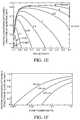
- FIGS. 1E and 1Fshow the photon conversion efficiency (i.e., the number of pump photons versus the number of output laser light photons) with increasing mirror reflectivity at various input optical power densities. Higher mirror reflectivity increases the optical power density within the laser cavity. At higher pump power densities, higher efficiencies result.
- FIG. 1Fshows photon conversion efficiencies as a function of pump power for various spot sizes, which shows the same trend of higher efficiency with optical density as does the graph shown in FIG. 1E. Spot size refers to the diameter of the optical pump in the optically active laser material.
- Table Ishows typical power usage and lifetime characteristics for a side pumped laser 100 as shown in FIG. 1A, an end-pumped laser 117 as is shown in FIG. 1C, and a lamp pumped laser.
- the diode end-pumped laser 117has the greater efficiency.
- end-pumped laser systemshave more optical components and therefore are difficult to align.
- the optical beam from a laser diode outputsis highly assymmetric. Therefore, light from the diodes is difficult to couple into the active material, e.g. laser material 101 , of an optical amplifier or a laser.
- the lifetimes, efficiency, and expense of various laser diode configurationsmake them very attractive as pump sources for optically active devices.
- Multimode laser diodesare highly desirable optical pump sources as they are inexpensive to manufacture and are capable of producing much higher power levels than single mode lasers. Multimode lasers are more reliable than single-mode lasers as they have lower output power densities reducing the risk of catastrophic facet damage, the primary cause of laser diode failure. However the light emitted by a multimode laser diode is very asymmetric. Typically, the laser diode emitting aperture has dimensions on the order of 1 ⁇ m ⁇ 100 ⁇ m. It is very difficult and costly to collect and couple light emitted by a multimode laser diode into the end facet of a single-mode optical waveguide or fiber.
- Most conventional waveguide amplifiers and lasersinclude one or more waveguide cores doped with active elements, such as Er, Yb, Nd and Tm, and are designed such that the waveguide can support coaxially propagating single-mode output and pump light.
- the output power of a single-mode, single laser pumped amplifier or laseris often limited to about 20 dBm (100 mW) by the power levels of available single-mode pump lasers.
- Single-mode pump lasersrequire more precision manufacturing tolerances and are consequently more expensive to produce than multimode lasers.
- Complex and costly schemesare required to pump arrays of waveguide optical amplifiers and lasers.
- Pump lighthas to be distributed to each amplifier channel or laser element, requiring combinations of splitters, combiners, taps, monitors and associated control electronics to effectively manage the distribution. Polarization sensitivity of waveguide elements further complicates the distribution process.
- an optical waveguide devicethat couples light from at least one laser diode into a high refractive index contrast slab waveguide.
- the high refractive index contrast slab waveguideincludes a light duct in a horizontal plane in order to receive light from the at least one laser diode.
- the high refractive index contrast slab waveguideincludes a high refractive index active waveguide and an intermediate refractive index passive cladding.
- the high refractive index contrast slab waveguideis folded in a horizontal axis.
- the intermediate passive claddingis thick enough in the vertical axis to capture a substantial amount of light from the at least one laser diode in the vertical direction.
- light transmitted from the optical waveguide deviceis efficiently coupled into single mode optical fibers by mode size converters.
- FIGS. 1A and 1Billustrate a side-pumped solid-state laser.
- FIGS. 1C and 1Dillustrate an end-pumped solid-state laser.
- FIGS. 1E and 1Fshow graphs illustrating higher pump efficiency with higher optical densities.
- FIG. 2illustrates the characteristics of a typical laser beam in a laser cavity.
- FIGS. 3A and 3Billustrate integration of photodetectors and laser diodes with planar waveguides.
- FIG. 4illustrates a butt-coupling technique for optically coupling between a laser diode and a waveguide.
- FIGS. 5A, 5B and 5 Cillustrate integrated coupling chips for coupling optical energy from a single mode laser diode chip.
- FIGS. 6A and 6Billustrate a coupling chip for coupling optical energy from a multi-mode laser diode array to a multi-mode optical fiber in accordance with the present invention.
- FIGS. 7A and 7Billustrate a coupling chip for coupling optical energy from a multi-mode laser diode array to a single mode optical fiber in accordance with the present invention.
- FIGS. 8A and 8Billustrate an embodiment of an amplifier chip according to the present invention.
- FIG. 9illustrates the optical materials utilized in waveguides according to the present invention.
- FIGS. 10A, 10B, and 10 Cillustrate an efficient mode size conversion for vertical pumping of an amplifier core.
- FIG. 11illustrates a monolithic array beam concentrator chip according to the present invention.
- FIGS. 12A and 12Billustrate the mode images for two example waveguides according to the present invention.
- FIG. 13illustrates a Vertical Cavity Surface Emitting Laser (VCSEL) pumped microchip laser according to the present invention.
- VCSELVertical Cavity Surface Emitting Laser
- Lasers and other light sourceshave great utility when able to produce high optical power densities
- the speed and effectiveness of the interaction of laser power or energy with materialsis in direct proportion to the brightness and intensity of the power or energy that the laser can deliver to the material.
- the highest brightness or intensity of a laser output beamis obtained when the beam is confined to the fundamental, lowest order transverse electromagnetic mode (TEM 00 ). Therefore, single transverse mode is the highest brightness form of a laser's output, which is the laser's most desirable property.
- TEM 00fundamental, lowest order transverse electromagnetic mode
- a high refractive refractive index contrast multimode slab waveguide of an appropriate design to collect and contain a high proportion of the light emitted by a single or multi-element multi-mode pump laser diode and efficiently couple that light into an assembly of actively doped single-mode waveguides embedded within the slabis presented.
- the light from the pump sourcethen, is efficiently coupled into one or more active regions through the effects of the differences in refractive index between the slab material of the waveguide and the cladding material around the slab.
- Both the slab material and the cladding materialcan be deposited with a high degree of uniformity and control in order to obtain the coupling.
- the embedded active core material of the waveguidecan also be manufactured with a high degree of uniformity and control.
- long, single-mode waveguidesare folded many times to accommodate lengths greater than the dimensions of the pumped, encapsulating multimode slab waveguide.
- the single-mode waveguide corescan be folded in such a manner as to optimize the effective absorption cross-section they present to the guided multimode pump light flux while minimizing losses due to bending experienced by propagating single-mode signal light.
- the efficiency of absorption of pump light from the multimode laser diodes by single-mode actively doped waveguide coresis a function of the ratio of the effective cross-section areas of the single-mode and multimode waveguides.
- the multimode slab waveguide itselfis pumped. This effect can result in a slap light source.
- the dimension of the multimode slab waveguideenables conservation of high power densities of the light emitted by the pump laser diode elements, while not increasing the difficultly and reducing the effectiveness of direct coupling between the laser diodes and the edge facet of the slab waveguide.
- High pump power densitiesare particularly important for three-level active systems where natural ground state absorption must first be bleached out before gain can be achieved.
- single-mode light emitted by the laser diode in its fast axis directioni.e., the direction of larger laser beam divergence
- multiple-mode lightimmediately after the light enters a slab waveguide, thereby limiting the return path for pump energy to the pump laser source.
- Lasing and optical amplification processesare processes of energy conversion. Energy is pumped into exciting active elements in the active material, where the energy is stored, from any energy source, commonly optical, which is capable of exciting the active elements. Energy stored in the excited active elements, then, is released when the excited active element is induced by a signal, such as when the active element is perturbed by presence of another photon, into releasing the energy in the form of an optical photon. For example, energy from the excited states of a laser material is released in a highly coherent form by stimulated emission. The efficiency of the conversion process is a key factor in determining the cost-effectiveness of a particular laser or optical amplification or conversion process.
- Planar waveguide forms of optical amplifiers and lasersare desirable as they are very compact compared to other forms of optical amplifiers and lasers.
- a planar waveguide formpotentially allows the integration of diverse optical and electronic functions on, for example, silicon wafers which can be manufactured in high volumes and at low cost with processes commonly used in the semiconductor-industry.
- slab emittersare desirable as efficient light sources.
- FIG. 3Aillustrates integration of an optical waveguide 301 with a photodetector (PD) 302 .
- Photodetector 302is formed on semiconducting layer 305 .
- An optical layer 303is formed over photodiode 302 and waveguide 301 is formed on optical layer 303 .
- Light traveling through waveguide 301can be coupled onto photodetector 302 at coupler 306 .
- FIG. 3Billustrates integration of pump laser diodes 310 with an active material waveguide 311 .
- laser waveguide 311is formed on an optical layer 313 .
- Optical layer 313is formed over laser diodes 310 , which are formed on semiconducting layer 312 .
- laser diodes 310can be formed to the side of optical waveguide 311 , over optical waveguide 311 , or in any other orientation with respect to optical waveguide 311 that allows pumping of the active dopant ions of optical waveguide 311 .
- FIG. 4illustrates coupling of a laser diode chip 410 with a high refractive index contrast (An) waveguide 411 .
- the method of coupling illustrated in FIG. 4is referred to as “butt coupling,” where laser diode 410 is a single-mode semiconductor laser diode output facet positioned to within about 5 ⁇ m of high An rectangular waveguide 411 in order to correct for mode astigmatism, thereby reducing coupling loss.
- about a 50% couplingcan be achieved with this method utilizing uncoated facets.
- customer demandis for greater than 80-85% coupling efficiency for laser diodes with complex, non-gaussian mode output profiles. Therefore, conventional butt-coupling techniques are not meeting customer demand.
- FIG. 5Aillustrates a laser coupling chip 501 that couples light from a laser diode 506 to an optical fiber 507 .
- Coupling chip 501includes a waveguide 502 with an integrated photodiode 503 to allow for down-stream power monitoring.
- photodiode 503may couple about 0.02 dB to about 0.05 dB of the optical power in waveguide 502 to provide optical coupling.
- a dual-core mode size converter 504can be formed in coupling chip 501 to optimize for efficient optical coupling to optical fiber 507 .
- Dual-core mode size converter 504can couple light to optical fiber with a coupling loss of about 0.25 dB.
- the resulting total loss of less than 1 dB in laser coupling chip 501results in a greater than 80% coupling efficiency between laser diode 506 and optical fiber 507 .
- the coupling efficiency between laser diode 506 and coupling chip 501is less than 80%.
- coupling chip 501can be formed on a millimeter-scale chip sized to fit a standard 14-pin butterfly package. Further, in order to achieve optimum coupling efficiencies, the slow-axis and fast-axis alignment between laser diode 506 and coupling chip 501 requires sub-micron positioning precision.
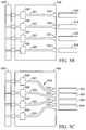
- FIG. 5Bshows a single mode laser diode array coupler chip 508 .
- Light from laser diode array 520is coupled into waveguides 521 , 522 , 523 , and 524 .
- Waveguides 521 , 522 , 523 and 524are each integrated with a photodetector 525 , 526 , 527 , and 528 , respectively, as is discussed above with regard to FIG. 5A.
- mode size converters 529 , 530 , 531 , and 532formed in waveguides 521 , 522 , 523 , and 524 , respectively, efficiently couple light into optical fibers 533 , 534 , 535 , and 536 , respectively.
- FIG. 5Cshows a single mode laser diode array coupler chip 509 similar to diode array coupler chip 508 with a pitch size converter 540 , which provides for closer packing of optical fibers 533 , 534 , 535 , and 536 .
- the arrangement proposed by Sipesinvolves an array of laser diodes arranged along the corners of a pumping path, for example a zig-zag pattern, such that pump power from multiple laser diodes are coupled into an active waveguide.
- the arrangement proposed by Baerincludes a side pumped active material block with zig-zagging of the signal bea, through the active material for maximum interaction.
- Lawrence Livermore National Labshas proposed a high output Yb:YAG laser system that utilizes a diode bar stack and a lens duct that brings the pump light from the diode bar stack into a Yb:YAG laser rod. About an 80% coupling efficiency can be achieved in this fashion. However, this solution requires a bulk laser rod and a large lens duct to direct light from the diode bar stack into the laser rod.
- Some embodiments of the present inventioncan utilize multimode laser diodes in the form of single elements or arrays, to efficiently pump compact, single-mode, planar waveguide optical amplifiers, lasers, and slab devices, which can be integrated with other optical and electronic functions and manufactured inexpensively in high volumes with semiconductor industry techniques.
- the output light from a multimode laser diode 610is single-mode in the vertical plane (the fast axis) and multimode in the horizontal plane (the slow axis). Therefore, the output beam diverges very rapidly in the vertical axis (the fast axis) but slowly diverges in the horizontal plane (the slow axis).
- FIGS. 6A and 6Billustrate coupling of light from a laser diode array into a planar waveguide in accordance with the present invention.
- the light beam from multimode laser diode array 610diverges less in the slow axis direction (shown in FIG. 6A) than it does in the fast axis direction (shown in FIG. 6B).
- the output beams from laser diode array 610diverge more in the vertical axis (shown in FIG. 6B) than in the horizontal axis (shown in FIG. 6A).
- Embodiments of the present inventiontake advantage of the slow divergence in the horizontal axis to increase the optical density in high refractive index waveguide 612 .
- Coupling chip 611can include a large lens duct 613 to direct light into high refractive index waveguide 612 .
- the material of waveguide 612 and lens duct 613can be the same material and can be deposited and patterned on a substrate in the same series of processing steps. Light from waveguide 612 can then be coupled into multimode fiber 614 .
- a higher optical power densitycan be achieved utilizing less expensive multimode laser diode bars, rather than single mode laser diode arrays, and coupling the optical output from multiple ones of the laser diodes in diode array 610 into waveguide 612 .
- Higher coupling efficiencyis achieved by utilizing a light duct 613 formed with waveguide 612 .
- the horizontal alignment between diode array 610 and coupling chip 611is not critical, so long as the light beams are directed toward duct 613 . As shown in FIG. 6B, alignment in the vertical axis (i.e., the fast axis) is somewhat critical because of the large divergence of the light output from diode array 610 in that direction.
- the pump light from the laser diodecan be constrained within the confines of the high An slab waveguide and therefore no critical alignment exists between the laser diode and the active waveguide, as would be true for conventional pumping configurations as has been discussed above. Further, there is no need to maintain single-mode propagation in the horizontal direction, as alignment tolerance are relaxed in the horizontal plane. In the vertical plane, a single optical mode can be excited to obtain maximum power density by using more precise alignment. When maximize power density is not required, the alignment tolerances in the vertical plane can also be relieved by using a thicker high refractive index contrast slab waveguide and allowing the light to propagate multimode in the vertical direction as well.
- FIGS. 7A and 7Billustrate coupling utilizing a double-clad core.
- light from one or more laser diodes 710 of multimode pump diode array 702is coupled into waveguide 703 of coupling chip 701 .
- a lens duct 704can be formed with waveguide 703 to direct light from laser diodes 710 in diode array 702 into waveguide 703 .
- light from waveguide 703can be coupled into single-mode fiber 705 .
- FIG. 7Bshows a cross-section of waveguide 703 .
- Waveguide 703includes a single-mode core 706 .
- Single-mode core 706can be formed, for example, from rare-earth doped Al 2 O 3 , Y 2 O 3 , or TiO 2 to form a high refractive index core.
- Single-mode core 706can be surrounded by a multi-mode cladding 707 having a lower refractive index than that of single-mode core 706 , which can be formed from an intermediate refractive index contrast material such as Al 2 O 3 or Y 2 O 3 .
- the dimensions of multi-mode cladding 707can capture most or all of the light output from laser diode array 702 .
- Waveguide 703can be formed on, for example, a silica or aluminasilicate buffer layer 709 deposited on a substrate.
- a second buffer layer 708can be formed over waveguide 703 .
- coupling chip 701can provide efficient conversion of low optical power density light emitted from directly-coupled multimode laser diode bars to high optical power density.
- high-refractive index contrast core 706is optically active
- a lasercan be formed by including a laser cavity, which can be formed by depositing mirrors on the ends of chip 701 .
- Very high optical-to-optical efficienciescan be achieved in coupling chip 701 .
- a multimode laser diode operating at a wavelength of 920 nmis efficiently coupled into a single-mode output laser at about 1100 nm utilizing an active waveguide 706 formed from double-clad Yb-doped silica, for example.
- a single mode active waveguide located in the high refractive index portion of the slabwill be efficiently pumped.
- Such active areasare shown, for example, in FIGS. 8A and 8B.
- the active region of the waveguidecan be “folded” or routed through many loops in order to increase the length of active material pumped and thereby increase the amplification in the waveguide.
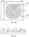
- FIGS. 8A and 8BAn embodiment of a folded active region embedded within the large high refractive index slab is shown in FIGS. 8A and 8B.
- any appropriate configuration or routing of active area waveguide within the slabcan be utilized.
- zig-zag configurationsmay also be utilized in addition to the spiral configuration shown in FIG. 8A.
- linear arrays of active regionsmay be utilized.
- FIG. 8Ashows the slow axis view (i.e., the horizontal view) and FIG. 8B shows the fast-axis view (i.e., the vertical cross section) of an active waveguide amplifier or laser chip 801 pumped by a multimode laser diode array in accordance with the present invention.
- a single mode high refractive index contrast core 803is arranged on chip 801 .
- a spiral arrangementis shown in FIG. 8A, any arrangement that provides a long signal path between a single mode input fiber 807 and a single mode output fiber 808 can be implemented.
- FIG. 8Bshows a cross section of an area of chip 801 with multiple crossings of single-mode high refractive index contrast active waveguide 803 .
- active waveguide 803can be formed from Yb-doped Al 2 O 3 , Y 2 O 3 or TiO 2 .
- Intermediate refractive index contrast cladding 804can be formed from Al 2 O 3 or Y 2 O 3 . In this arrangement, a high pump-power density can be achieved in multi-mode cladding 804 , which results in highly efficient pumping of active waveguide 803 .
- Multi-port amplifierscan be obtained by routing multiple folded regions of active waveguide such as waveguide 803 within the high An slab 804 of chip 801 .
- multiple active coresmay be routed together as shown in FIG. 8A.
- a single multimode pumptherefore, can be shared among several single-mode active amplifying waveguides without the need to split the pump light and separately distribute the light to activate the single-mode amplifying waveguides separately. There is, therefore, no need for pump splitters or multiplexers. Further, the higher area of the active region increases absorption of the pump light, reducing the need for mirrors to rout the pump light through the active regions multiple times.
- FIG. 9illustrates material depositions that provide high grade, optically transparent, highly uniform slab waveguides with highly controllable An values.
- the production of such waveguidesis further discussed in U.S. application Ser. No. 09/903,081, “As-Deposited Optical Waveguides with Low Scattering Loss and Methods for Their Manufacture,” by Demaray et al, filed on Jul. 10, 2001; U.S. application Ser. No. 10/101,863, “Biased Pulse DC Sputtering of Oxide Films, by Zhang et al., filed on Mar. 16, 2002; U.S. application Ser. No.
- Waveguide materials used to form active core waveguides, passive waveguides, and claddings consistent with embodiments of the present inventioncan be deposited by biased pulsed DC plasma vapor deposition (PVD), as described in U.S. application Ser. No. 10/101,341 (the '341 application).
- the physical characteristics of the optical material deposited by biased pulsed DC PVDdepends on various process parameters, as discussed in the '341 application.
- a device, including photodetectors and other electronics, such as those shown in FIGS. 3A through 8B and discussed above,can be fabricated by depositing one or more active or passive optical layers and patterning the optical layers to form the waveguides and lens ducts as shown. In some applications, several deposition and patterning steps may be applied to form the desired structures.
- FIG. 9shows active and passive waveguide materials of highly amorphous, defect free films of aluminasilicated deposited by biased pulsed DC PVD.
- the filmshave very high optical transparency, for example below 0.3 db/cm loss and, in some deposited films, less than about 0.1 db/cm loss. Therefore, deposition of films utilizing biased pulsed-DC PVD are useful for providing structures for optical coupling devices, optical amplifiers, and optical laser structures for highly efficient coupling of pump sources as has been discussed above.
- depositionis performed in a vacuum deposition chamber.
- a substrateis mounted on a support which also provides an RF bias voltage to the substrate.
- RF poweris supplied to a target formed from material to be deposited as gas is allowed into the chamber.
- a plasmais excited in the gas and the material is deposited on the substrate.
- a pulsed DC signalis provided to the target. Further details regarding the deposition process are provided in the '341 application.
- FIGS. 10A, 10B, and 10 CCoupling of light, for example from optical fiber 807 into waveguide 803 , through efficient mode size conversion is illustrated in FIGS. 10A, 10B, and 10 C.
- Vertically tapered mode-size conversionis further discussed in U.S. application Ser. No. 10/101,492, “Mode Size Converter for a Planar Waveguide,” by Tao et al, filed on Mar. 16, 2002, herein incorporated by reference in its entirety.
- a very smooth vertical tapercan efficiently couple light from optical fiber 807 into high refractive index contrast, core waveguide 803 very efficiently.
- FIG. 10Bshows the mode size of an optical beam at a point where light enters waveguide 803 .
- FIG. 10Bshows a significantly smaller mode size in the region of waveguide 803 after the adiabatic S-taper mode size converter 1001 .
- Mode size converter 1001can be produced in a biased pulsed-DC PVD process with a shadow mask.
- Table IIshows modeling of mode diameter at the output facet of a mode converter for various core/cladding refractive index contrasts An.
- the dimensions in Table IIrefer to the dimensions of the output facet of the rectangular mode converter.
- TABLE II1.0 ⁇ m ⁇ 1.5 ⁇ m ⁇ ⁇ n 1.0 ⁇ m 1.5 ⁇ m 2.0 ⁇ m ⁇ 2.0 ⁇ m 2.5 ⁇ m ⁇ 2.5 ⁇ m 0.43% 38 ⁇ m 35 ⁇ m 14 ⁇ m 6 ⁇ m 0.3% 36 ⁇ m 20 ⁇ m 16 ⁇ m 0.2% 32 ⁇ m 24 ⁇ m
- FIG. 11illustrates an image concentrator 1101 for adiabatically compressing the diameter of the mode output by a passively Q-switched microchip laser array.
- Image concentrator 1101employs a reverse taper 1106 , such as that first disclosed in U.S. application Ser. No. 10/101,492 to Tao et al.
- Reverse taper 1106can be formed vertically and/or horizontally and thereby provides coupling into a smaller mode size.
- a further embodimentincludes a pitch size conversion such as that illustrated in FIG. 5C.
- Embodiments of the inventionenable the mode size and pitch size conversion of individually addressable microchip laser array, so as to be tailored to standard print pixel densities for use in direct printing and micromaching applications.
- Image concentrator 1101can include an addressable array pump bar 1102 which is capable of addressing and exciting individual pixels of a microchip bar 1103 .
- Array pump bar 1102includes an array of laser diodes which produce light when individually addressed.
- Microchip bar 1103which provides amplification as was discussed in FIGS. 6 - 8 .
- Beam concentrator chip 1104can include light ducts or vertical tapers in order to collect a substantial amount of light from microchip bar 1103 .
- a vertical reverse taper 1106as is described in U.S. application Ser. No. 10/101,492, allows for a compressed output mode. As shown in FIG.
- a monolithic array beam concentrator chipcan convert 50 ⁇ m or 90 ⁇ m diameter single mode spots from microchip bar 1103 into 20 to 25 ⁇ m diameter spots.
- FIGS. 12A and 12Bshow mode sizes for some weakly-confined mode propagation in waveguides.
- FIG. 12Aillustrates a 6.2 ⁇ m mode diameter at the output facet of a 1.5 ⁇ m ⁇ 3.5 ⁇ m waveguide for 980 nm light with a refractive index contrast An between the core and the cladding of about 1%.
- FIG. 12Billustrates a 7.6 ⁇ m mode diameter at the output facet of a 1.25 ⁇ m ⁇ 3.5 ⁇ m waveguide for 980 nm light with a refractive index contrast of about 1%.
- the optical energyis concentrated in the center of the facet.
- Table IIIillustrates facet damage considerations in a image concentrator such as image concentrator 1101 shown in FIG. 11.
- Table IIIillustrates, for representative pixel densities, the mode size required, the distance between modes, and the resulting power density in image concentrator 1101 .
- the value of 14.2 for power density shown for 2400 dpi pixel densityexceeds the damage threshold of Quartz.
- TABLE IIIPixel Density Mode Pitch/Mode Power Density at Collimation Distance (dpi) Size Facet (GW cm ⁇ 2 ) ( ⁇ m) 600 42 0.9 842 1200 21 3.6 210 2400 11 14.2 53
- FIG. 13illustrates a vertical cavity surface emitting laser (VCSEL)-pumped microchip 1401 according to the present invention.
- VCSELs 1401can be deposited on a GaAs substrate 1402 .
- VCSELs 1401include a dichroic output facet coating.
- An active gain medium 1404can be deposited directly over VCSELs 1403 .
- Active gain medium 1404can be, for example, Nd, Yb, Er, Tm, Ho, Pr, or Ce doped silica.
- a saturable absorber 1405can be deposited over gain medium 1404 .
- Saturable absorber 1405can be, for example, a Cr4+ or Co2+ doped silica film.
- a VCSEL pumped microchip 1401can be fabricated using high volume wafer-scale semiconductor manufacturing techniques.
- the doped silica used for saturable absorber 1405 and active gain medium 1404can be deposited by biased pulsed-DC PVD processing techniques.
Landscapes
- Physics & Mathematics (AREA)
- Optics & Photonics (AREA)
- Engineering & Computer Science (AREA)
- Electromagnetism (AREA)
- General Physics & Mathematics (AREA)
- Plasma & Fusion (AREA)
- Microelectronics & Electronic Packaging (AREA)
- Lasers (AREA)
- Optical Couplings Of Light Guides (AREA)
Abstract
Description
- This application claims priority to provisional application Ser. No. 60/406,451, entitled “Efficient Method of Coupling to a Multimode Laser Diode in Order to Optically Pump a Single-Mode Optical Signal Amplifier or Laser,” filed Aug. 27, 2002, by David Dawes, herein incorporated by reference in its entirety.[0001]
- 1. Technical Area[0002]
- The present invention relates to coupling of pump light into an optical amplifier or a laser and, in particular, to coupling from a multimode laser diode in order to optically pump an optical amplifier or laser.[0003]
- 2. Discussion of Related Art[0004]
- Use of directed energy beams, such as those produced by amplifiers or lasers, are diverse and include applications in a wide range of fields, including biotechnology, medicine, semiconductor processing, manufacturing, image recording and defense. In biotechnology, directed energy beams are used, for example, in flow cytometry, DNA sequencing, confocal microscopy, and hematology. Medical applications include use in ophthalmology, non-invasive surgery, and photodynamic therapy. In the semiconductor industry, applications include wafer inspection, rapid thermal processing, and scribing or marking. Image recording applications include, for example, high-speed printing, photo-processing, film subtitling and holography. Industrial applications include, for example, rapid prototyping, materials processing and scribing or marking. Additionally, military applications include range finding, target designation, lidar, and chemical or biological threat detection. The graphics and printing industry, one of the largest businesses in the world, has a need for inexpensive laser systems for use in applications such as thermal graphics. Such applications require a highly reliable, low noise laser or optical amplifier at a low cost.[0005]
- Typically, applications for directed energy beams require a laser or optical amplifier. An optical amplifier differs from a laser by the absence of a laser cavity. Both devices typically require an active optical material, for example rare-earth doped YAG, ruby (Al[0006]2O3:Cr), or other material, which can be optically “pumped,” such that energy can be stored in the excited states of the active atoms or molecules by an optical pump source. Amplification of input optical radiation or stimulated emission for lasing then occurs when the same optical energy stored in the excited states is coupled to the incident optical beam.
- FIG. 1A shows an example of a side-pumped[0007]
laser 100.Laser material 101 is positioned in a laser cavity defined bymirrors diode array 104.Diode array 104 includes a series of laser diodes105-1 through105-N positioned to illuminate all or most oflaser material 101. There are a variety of choices for laser diodes and laser diode arrays available to pump Nd or Yb doped YAG, for example. In most applications, Nd:YAG is pumped at about 808 nm and Yb:YAG is pumped at about 940 nm. Choices fordiode array 104 include 10-40W arrays, 40-50W single bars, and 240-600W stacked bars, for example. Arrays can also be formed from readily available 1-2W single laser diodes. - FIG. 1B illustrates the optical density in a cross section of[0008]
laser material 101 in side-pumpedlaser 100 of FIG. 1A. As is shown in FIG. 1B, the optical density is greatest in the center oflaser material 101 where the laser beam is located. However, much of the pump energy is dissipated in areas oflaser material 101 that are not actively involved in the lasing process. Therefore, side pumping techniques are inherently inefficient. - As is illustrated in FIG. 1A, the laser beam is directed between[0009]
mirrors mirror 103. FIG. 2 illustrates the shape of a laser beam in a laser cavity such as inlaser 100. The closer the laser beam is to its diffraction limit inlaser material 101, the greater the depth of field and the smaller the diameter of beam handling optics (forexample mirrors 102 and103) required to transmit the beam. The ratio of the divergence of the laser beam to that of a theoretically diffraction limited beam of the same waist size in the TEM00mode is usually given as M2=(θ/θ), where Θ is the divergence angle of the laser beam and θ is the divergence angle of the theoretical laser beam. The angular size of the laser beam in the far field will be M2times the size calculated for a perfect Gaussian beam, i.e. θ=M2(2λ/W0) for a beam waist diameter of 2W0. - FIG. 1C illustrates an end-pumping arrangement for pumping[0010]
laser material 101. In the arrangement shown in FIG. 1C,laser material 101 is again placed in a laser cavity formed bymirrors mirror 103 is reflected by adichroic beam splitter 114 to form the beam. Optical energy frompump source 116 is incident onlens 115 and passes throughdichroic beam splitter 114 andmirror 103 to Locus in a nearly diffraction limited region oflaser material 101. The beam frompump source 116 is reduced to a size and shape that resembles the shape of the laser beam shown in FIG. 2 inactive material 101. Additionally, asecond pump source 110 can be focused bylens 113 throughmirror 102 and intolaser material 101. In some embodiments, additional optical energy can be coupled intolaser material 101 frompump source 111 using a polarizingbeam splitting cube 112, which transmits light frompump source 110 while reflecting light frompump source 111. - A cross section of[0011]
laser material 101 illustrating optical power concentration is shown in FIG. 1D. As can be seen in FIG. 1D, nearly all of the pump power, as well as the laser beam, is focused in the active region oflaser material 101, where the laser beam produced bylaser 117 is produced. - As is pointed out in U.S. Pat. No. 4,710,940 to D. L. Sipes, Jr, issued on Dec. 1, 1987, to a first approximation, and not being limited by theory, the higher the pump power density the more efficient is the use of pump power. This concept is illustrated in the graphs shown in FIGS. 1E and 1F. FIG. 1E shows the photon conversion efficiency (i.e., the number of pump photons versus the number of output laser light photons) with increasing mirror reflectivity at various input optical power densities. Higher mirror reflectivity increases the optical power density within the laser cavity. At higher pump power densities, higher efficiencies result. FIG. 1F shows photon conversion efficiencies as a function of pump power for various spot sizes, which shows the same trend of higher efficiency with optical density as does the graph shown in FIG. 1E. Spot size refers to the diameter of the optical pump in the optically active laser material.[0012]
- Table I shows typical power usage and lifetime characteristics for a side pumped[0013]
laser 100 as shown in FIG. 1A, an end-pumpedlaser 117 as is shown in FIG. 1C, and a lamp pumped laser. As expected, the diode end-pumpedlaser 117 has the greater efficiency. However, end-pumped laser systems have more optical components and therefore are difficult to align. - Typically, the optical beam from a laser diode outputs is highly assymmetric. Therefore, light from the diodes is difficult to couple into the active material,[0014]
e.g. laser material 101, of an optical amplifier or a laser. However, as shown in Table I, the lifetimes, efficiency, and expense of various laser diode configurations make them very attractive as pump sources for optically active devices.TABLE I Lamp Diode End- Diode Side- Pumped Pumped Pumped Power to Pump 5000 W 2.5 W 50 W Source Power to Cooling 500 W 2.5 W 50 W System Power from Pump 3500 W 1.25 W 20 W Source Single-Mode 10 W 0.8 W 10 W Power from Laser Wall-Plug Effi- 0.2% 16% 10% ciency Cooling Water Free Air Forced Air Power Consumed/ 500 kW-hr 6.5 kW-hr 10 kW-hr Output kW-hr Cost of Light $200 $400 $1000 Source Lifetime of Light 200 hrs 20,000 hrs 10,000 hrs Source - Multimode laser diodes are highly desirable optical pump sources as they are inexpensive to manufacture and are capable of producing much higher power levels than single mode lasers. Multimode lasers are more reliable than single-mode lasers as they have lower output power densities reducing the risk of catastrophic facet damage, the primary cause of laser diode failure. However the light emitted by a multimode laser diode is very asymmetric. Typically, the laser diode emitting aperture has dimensions on the order of 1 μm×100 μm. It is very difficult and costly to collect and couple light emitted by a multimode laser diode into the end facet of a single-mode optical waveguide or fiber.[0015]
- Most conventional waveguide amplifiers and lasers include one or more waveguide cores doped with active elements, such as Er, Yb, Nd and Tm, and are designed such that the waveguide can support coaxially propagating single-mode output and pump light. The output power of a single-mode, single laser pumped amplifier or laser is often limited to about 20 dBm (100 mW) by the power levels of available single-mode pump lasers. Single-mode pump lasers require more precision manufacturing tolerances and are consequently more expensive to produce than multimode lasers. As a result complex and costly schemes are required to pump arrays of waveguide optical amplifiers and lasers. Pump light has to be distributed to each amplifier channel or laser element, requiring combinations of splitters, combiners, taps, monitors and associated control electronics to effectively manage the distribution. Polarization sensitivity of waveguide elements further complicates the distribution process.[0016]
- Therefore, there is a need for optical laser devices capable of efficiently coupling light from a laser diode into the active region of a laser cavity that is cost effective and reliable, and that produces high optical output power.[0017]
- In accordance with the present invention, an optical waveguide device that couples light from at least one laser diode into a high refractive index contrast slab waveguide is presented. In some embodiments, the high refractive index contrast slab waveguide includes a light duct in a horizontal plane in order to receive light from the at least one laser diode. In some embodiments, the high refractive index contrast slab waveguide includes a high refractive index active waveguide and an intermediate refractive index passive cladding.[0018]
- In some embodiments, the high refractive index contrast slab waveguide is folded in a horizontal axis. In some embodiments, the intermediate passive cladding is thick enough in the vertical axis to capture a substantial amount of light from the at least one laser diode in the vertical direction. In some embodiments, light transmitted from the optical waveguide device is efficiently coupled into single mode optical fibers by mode size converters.[0019]
- These and other aspects of the present invention are further described in the following figures.[0020]
- FIGS. 1A and 1B illustrate a side-pumped solid-state laser.[0021]
- FIGS. 1C and 1D illustrate an end-pumped solid-state laser.[0022]
- FIGS. 1E and 1F show graphs illustrating higher pump efficiency with higher optical densities.[0023]
- FIG. 2 illustrates the characteristics of a typical laser beam in a laser cavity.[0024]
- FIGS. 3A and 3B illustrate integration of photodetectors and laser diodes with planar waveguides.[0025]
- FIG. 4 illustrates a butt-coupling technique for optically coupling between a laser diode and a waveguide.[0026]
- FIGS. 5A, 5B and[0027]5C illustrate integrated coupling chips for coupling optical energy from a single mode laser diode chip.
- FIGS. 6A and 6B illustrate a coupling chip for coupling optical energy from a multi-mode laser diode array to a multi-mode optical fiber in accordance with the present invention.[0028]
- FIGS. 7A and 7B illustrate a coupling chip for coupling optical energy from a multi-mode laser diode array to a single mode optical fiber in accordance with the present invention.[0029]
- FIGS. 8A and 8B illustrate an embodiment of an amplifier chip according to the present invention.[0030]
- FIG. 9 illustrates the optical materials utilized in waveguides according to the present invention.[0031]
- FIGS. 10A, 10B, and[0032]10C illustrate an efficient mode size conversion for vertical pumping of an amplifier core.
- FIG. 11 illustrates a monolithic array beam concentrator chip according to the present invention.[0033]
- FIGS. 12A and 12B illustrate the mode images for two example waveguides according to the present invention.[0034]
- FIG. 13 illustrates a Vertical Cavity Surface Emitting Laser (VCSEL) pumped microchip laser according to the present invention.[0035]
- Lasers and other light sources have great utility when able to produce high optical power densities The speed and effectiveness of the interaction of laser power or energy with materials is in direct proportion to the brightness and intensity of the power or energy that the laser can deliver to the material. The highest brightness or intensity of a laser output beam is obtained when the beam is confined to the fundamental, lowest order transverse electromagnetic mode (TEM[0036]00). Therefore, single transverse mode is the highest brightness form of a laser's output, which is the laser's most desirable property.
- In accordance with some embodiments of the present invention, a high refractive refractive index contrast multimode slab waveguide of an appropriate design to collect and contain a high proportion of the light emitted by a single or multi-element multi-mode pump laser diode and efficiently couple that light into an assembly of actively doped single-mode waveguides embedded within the slab is presented. The light from the pump source, then, is efficiently coupled into one or more active regions through the effects of the differences in refractive index between the slab material of the waveguide and the cladding material around the slab. Both the slab material and the cladding material can be deposited with a high degree of uniformity and control in order to obtain the coupling. Further, the embedded active core material of the waveguide can also be manufactured with a high degree of uniformity and control.[0037]
- In some embodiments of the invention, long, single-mode waveguides are folded many times to accommodate lengths greater than the dimensions of the pumped, encapsulating multimode slab waveguide. The single-mode waveguide cores can be folded in such a manner as to optimize the effective absorption cross-section they present to the guided multimode pump light flux while minimizing losses due to bending experienced by propagating single-mode signal light. The efficiency of absorption of pump light from the multimode laser diodes by single-mode actively doped waveguide cores is a function of the ratio of the effective cross-section areas of the single-mode and multimode waveguides.[0038]
- In some embodiments of the invention, the multimode slab waveguide itself is pumped. This effect can result in a slap light source.[0039]
- In some embodiments, the dimension of the multimode slab waveguide enables conservation of high power densities of the light emitted by the pump laser diode elements, while not increasing the difficultly and reducing the effectiveness of direct coupling between the laser diodes and the edge facet of the slab waveguide. High pump power densities are particularly important for three-level active systems where natural ground state absorption must first be bleached out before gain can be achieved.[0040]
- In some embodiments single-mode light emitted by the laser diode in its fast axis direction (i.e., the direction of larger laser beam divergence) is converted to multiple-mode light immediately after the light enters a slab waveguide, thereby limiting the return path for pump energy to the pump laser source. Such an arrangement increases the pumping efficiency because more light is available for pumping.[0041]
- Lasing and optical amplification processes are processes of energy conversion. Energy is pumped into exciting active elements in the active material, where the energy is stored, from any energy source, commonly optical, which is capable of exciting the active elements. Energy stored in the excited active elements, then, is released when the excited active element is induced by a signal, such as when the active element is perturbed by presence of another photon, into releasing the energy in the form of an optical photon. For example, energy from the excited states of a laser material is released in a highly coherent form by stimulated emission. The efficiency of the conversion process is a key factor in determining the cost-effectiveness of a particular laser or optical amplification or conversion process.[0042]
- Planar waveguide forms of optical amplifiers and lasers are desirable as they are very compact compared to other forms of optical amplifiers and lasers. In addition, a planar waveguide form potentially allows the integration of diverse optical and electronic functions on, for example, silicon wafers which can be manufactured in high volumes and at low cost with processes commonly used in the semiconductor-industry. In addition to waveguides, slab emitters are desirable as efficient light sources.[0043]
- FIG. 3A, for example, illustrates integration of an[0044]
optical waveguide 301 with a photodetector (PD)302.Photodetector 302 is formed onsemiconducting layer 305. Anoptical layer 303 is formed overphotodiode 302 andwaveguide 301 is formed onoptical layer 303. Light traveling throughwaveguide 301 can be coupled ontophotodetector 302 atcoupler 306. - FIG. 3B illustrates integration of[0045]
pump laser diodes 310 with anactive material waveguide 311. As shown in FIG. 3B,laser waveguide 311 is formed on anoptical layer 313.Optical layer 313 is formed overlaser diodes 310, which are formed onsemiconducting layer 312. In some embodiments,laser diodes 310 can be formed to the side ofoptical waveguide 311, overoptical waveguide 311, or in any other orientation with respect tooptical waveguide 311 that allows pumping of the active dopant ions ofoptical waveguide 311. - FIG. 4 illustrates coupling of a[0046]
laser diode chip 410 with a high refractive index contrast (An)waveguide 411. The method of coupling illustrated in FIG. 4 is referred to as “butt coupling,” wherelaser diode 410 is a single-mode semiconductor laser diode output facet positioned to within about 5 μm of high Anrectangular waveguide 411 in order to correct for mode astigmatism, thereby reducing coupling loss. In some embodiments, about a 50% coupling can be achieved with this method utilizing uncoated facets. Unfortunately, customer demand is for greater than 80-85% coupling efficiency for laser diodes with complex, non-gaussian mode output profiles. Therefore, conventional butt-coupling techniques are not meeting customer demand. - FIG. 5A illustrates a[0047]
laser coupling chip 501 that couples light from alaser diode 506 to anoptical fiber 507.Coupling chip 501 includes awaveguide 502 with anintegrated photodiode 503 to allow for down-stream power monitoring. In some embodiments,photodiode 503 may couple about 0.02 dB to about 0.05 dB of the optical power inwaveguide 502 to provide optical coupling. A dual-coremode size converter 504 can be formed incoupling chip 501 to optimize for efficient optical coupling tooptical fiber 507. Dual-coremode size converter 504 can couple light to optical fiber with a coupling loss of about 0.25 dB. The resulting total loss of less than 1 dB inlaser coupling chip 501 results in a greater than 80% coupling efficiency betweenlaser diode 506 andoptical fiber 507. However, there remains the problem that the coupling efficiency betweenlaser diode 506 andcoupling chip 501 is less than 80%. - In some embodiments,[0048]
coupling chip 501 can be formed on a millimeter-scale chip sized to fit a standard 14-pin butterfly package. Further, in order to achieve optimum coupling efficiencies, the slow-axis and fast-axis alignment betweenlaser diode 506 andcoupling chip 501 requires sub-micron positioning precision. - FIG. 5B shows a single mode laser diode[0049]
array coupler chip 508. Light fromlaser diode array 520 is coupled intowaveguides Waveguides photodetector mode size converters waveguides optical fibers diode array 520, then, is coupled throughoptical fibers optical fibers array coupler chip 509 similar to diodearray coupler chip 508 with apitch size converter 540, which provides for closer packing ofoptical fibers - Other pumping schemes are described, for example, in U.S. Pat. No. 6,236,793, issued to Lawrence et al. on May 22, 2001; U.S. Pat. No. 4,710,940, issued to Sipes; U.S. Pat. No. 4,785,459 issued to Baer on Nov. 15, 1988; and at Lawrence Livermore National Labs. In a system proposed by Lawrence, et al., the pump light is reflected into the active waveguide core by reflecting the pump beam from a prism. Signal power is then transmitted through the prism into the waveguide core. However, in this configuration alignment of the optics directing the pump power into the waveguide core for efficient pumping needs to be arranged such that the waist of the beam is incident on the waveguide core. This results in a large alignment problem for efficiently coupling the pump power into the waveguide core. The arrangement proposed by Sipes involves an array of laser diodes arranged along the corners of a pumping path, for example a zig-zag pattern, such that pump power from multiple laser diodes are coupled into an active waveguide. The arrangement proposed by Baer includes a side pumped active material block with zig-zagging of the signal bea, through the active material for maximum interaction.[0050]
- Lawrence Livermore National Labs has proposed a high output Yb:YAG laser system that utilizes a diode bar stack and a lens duct that brings the pump light from the diode bar stack into a Yb:YAG laser rod. About an 80% coupling efficiency can be achieved in this fashion. However, this solution requires a bulk laser rod and a large lens duct to direct light from the diode bar stack into the laser rod.[0051]
- Some embodiments of the present invention can utilize multimode laser diodes in the form of single elements or arrays, to efficiently pump compact, single-mode, planar waveguide optical amplifiers, lasers, and slab devices, which can be integrated with other optical and electronic functions and manufactured inexpensively in high volumes with semiconductor industry techniques. As shown in FIGS. 6A and 6B, the output light from a[0052]
multimode laser diode 610 is single-mode in the vertical plane (the fast axis) and multimode in the horizontal plane (the slow axis). Therefore, the output beam diverges very rapidly in the vertical axis (the fast axis) but slowly diverges in the horizontal plane (the slow axis). - FIGS. 6A and 6B illustrate coupling of light from a laser diode array into a planar waveguide in accordance with the present invention. As shown in FIGS. 6A and 6B, the light beam from multimode[0053]
laser diode array 610 diverges less in the slow axis direction (shown in FIG. 6A) than it does in the fast axis direction (shown in FIG. 6B). The output beams fromlaser diode array 610 diverge more in the vertical axis (shown in FIG. 6B) than in the horizontal axis (shown in FIG. 6A). Embodiments of the present invention take advantage of the slow divergence in the horizontal axis to increase the optical density in highrefractive index waveguide 612.Coupling chip 611 can include alarge lens duct 613 to direct light into highrefractive index waveguide 612. The material ofwaveguide 612 andlens duct 613 can be the same material and can be deposited and patterned on a substrate in the same series of processing steps. Light fromwaveguide 612 can then be coupled intomultimode fiber 614. - A higher optical power density, then, can be achieved utilizing less expensive multimode laser diode bars, rather than single mode laser diode arrays, and coupling the optical output from multiple ones of the laser diodes in[0054]
diode array 610 intowaveguide 612. Higher coupling efficiency is achieved by utilizing alight duct 613 formed withwaveguide 612. Further, the horizontal alignment betweendiode array 610 andcoupling chip 611 is not critical, so long as the light beams are directed towardduct 613. As shown in FIG. 6B, alignment in the vertical axis (i.e., the fast axis) is somewhat critical because of the large divergence of the light output fromdiode array 610 in that direction. - The pump light from the laser diode can be constrained within the confines of the high An slab waveguide and therefore no critical alignment exists between the laser diode and the active waveguide, as would be true for conventional pumping configurations as has been discussed above. Further, there is no need to maintain single-mode propagation in the horizontal direction, as alignment tolerance are relaxed in the horizontal plane. In the vertical plane, a single optical mode can be excited to obtain maximum power density by using more precise alignment. When maximize power density is not required, the alignment tolerances in the vertical plane can also be relieved by using a thicker high refractive index contrast slab waveguide and allowing the light to propagate multimode in the vertical direction as well.[0055]
- FIGS. 7A and 7B illustrate coupling utilizing a double-clad core. As shown in FIG. 7A, light from one or[0056]
more laser diodes 710 of multimodepump diode array 702 is coupled intowaveguide 703 ofcoupling chip 701. Again, alens duct 704 can be formed withwaveguide 703 to direct light fromlaser diodes 710 indiode array 702 intowaveguide 703. Incoupling chip 701, light fromwaveguide 703 can be coupled into single-mode fiber 705. - FIG. 7B shows a cross-section of[0057]
waveguide 703.Waveguide 703 includes a single-mode core 706. Single-mode core 706 can be formed, for example, from rare-earth doped Al2O3, Y2O3, or TiO2to form a high refractive index core. Single-mode core 706 can be surrounded by amulti-mode cladding 707 having a lower refractive index than that of single-mode core 706, which can be formed from an intermediate refractive index contrast material such as Al2O3or Y2O3. In some embodiments, the dimensions ofmulti-mode cladding 707 can capture most or all of the light output fromlaser diode array 702.Waveguide 703 can be formed on, for example, a silica oraluminasilicate buffer layer 709 deposited on a substrate. Asecond buffer layer 708 can be formed overwaveguide 703. - In this way,[0058]
coupling chip 701 can provide efficient conversion of low optical power density light emitted from directly-coupled multimode laser diode bars to high optical power density. Where high-refractiveindex contrast core 706 is optically active, a laser can be formed by including a laser cavity, which can be formed by depositing mirrors on the ends ofchip 701. - Very high optical-to-optical efficiencies (e.g., greater than 80%) can be achieved in[0059]
coupling chip 701. For example, a multimode laser diode operating at a wavelength of 920 nm, is efficiently coupled into a single-mode output laser at about 1100 nm utilizing anactive waveguide 706 formed from double-clad Yb-doped silica, for example. - Having efficiently coupled the multimode pump light into a high refractive index slab waveguide which is multimode in the horizontal plane and may or may not be single mode in the vertical plane, a single mode active waveguide located in the high refractive index portion of the slab will be efficiently pumped. Such active areas are shown, for example, in FIGS. 8A and 8B. In some embodiments, the active region of the waveguide can be “folded” or routed through many loops in order to increase the length of active material pumped and thereby increase the amplification in the waveguide.[0060]
- An embodiment of a folded active region embedded within the large high refractive index slab is shown in FIGS. 8A and 8B. One skilled in the art will recognize that any appropriate configuration or routing of active area waveguide within the slab can be utilized. For example, zig-zag configurations may also be utilized in addition to the spiral configuration shown in FIG. 8A. Additionally, linear arrays of active regions may be utilized.[0061]
- FIG. 8A shows the slow axis view (i.e., the horizontal view) and FIG. 8B shows the fast-axis view (i.e., the vertical cross section) of an active waveguide amplifier or[0062]
laser chip 801 pumped by a multimode laser diode array in accordance with the present invention. As shown in FIG. 8A, a single mode high refractiveindex contrast core 803 is arranged onchip 801. Although a spiral arrangement is shown in FIG. 8A, any arrangement that provides a long signal path between a singlemode input fiber 807 and a singlemode output fiber 808 can be implemented. Light output fromlaser diode array 802 is captured by an intermediate refractive indexcontrast cladding layer 804 in which the single-mode high refractive index contrastactive waveguide 803 is embedded. FIG. 8B shows a cross section of an area ofchip 801 with multiple crossings of single-mode high refractive index contrastactive waveguide 803. As an example,active waveguide 803 can be formed from Yb-doped Al2O3, Y2O3or TiO2. Intermediate refractiveindex contrast cladding 804 can be formed from Al2O3or Y2O3. In this arrangement, a high pump-power density can be achieved inmulti-mode cladding 804, which results in highly efficient pumping ofactive waveguide 803. - Multi-port amplifiers can be obtained by routing multiple folded regions of active waveguide such as[0063]
waveguide 803 within the high Anslab 804 ofchip 801. For example, multiple active cores may be routed together as shown in FIG. 8A. A single multimode pump, therefore, can be shared among several single-mode active amplifying waveguides without the need to split the pump light and separately distribute the light to activate the single-mode amplifying waveguides separately. There is, therefore, no need for pump splitters or multiplexers. Further, the higher area of the active region increases absorption of the pump light, reducing the need for mirrors to rout the pump light through the active regions multiple times. - FIG. 9 illustrates material depositions that provide high grade, optically transparent, highly uniform slab waveguides with highly controllable An values. The production of such waveguides is further discussed in U.S. application Ser. No. 09/903,081, “As-Deposited Optical Waveguides with Low Scattering Loss and Methods for Their Manufacture,” by Demaray et al, filed on Jul. 10, 2001; U.S. application Ser. No. 10/101,863, “Biased Pulse DC Sputtering of Oxide Films, by Zhang et al., filed on Mar. 16, 2002; U.S. application Ser. No. 10/101,341, “Rare-Earth Pre-Alloyed PVD Targets for Dielectric Planar Applications,” by Milonopoulou et al., filed on Mar. 16, 2002; and application Ser. No. 09/633,307, “Planar Optical Devices and Methods for their Manufacture,” by Demaray et al., filed on Aug. 7, 2000, each of which is incorporated by reference herein in its entirety.[0064]
- Waveguide materials used to form active core waveguides, passive waveguides, and claddings consistent with embodiments of the present invention can be deposited by biased pulsed DC plasma vapor deposition (PVD), as described in U.S. application Ser. No. 10/101,341 (the '341 application). The physical characteristics of the optical material deposited by biased pulsed DC PVD depends on various process parameters, as discussed in the '341 application. A device, including photodetectors and other electronics, such as those shown in FIGS. 3A through 8B and discussed above, can be fabricated by depositing one or more active or passive optical layers and patterning the optical layers to form the waveguides and lens ducts as shown. In some applications, several deposition and patterning steps may be applied to form the desired structures.[0065]
- As shown in FIG. 9, which shows active and passive waveguide materials of highly amorphous, defect free films of aluminasilicated deposited by biased pulsed DC PVD. Further, the films have very high optical transparency, for example below 0.3 db/cm loss and, in some deposited films, less than about 0.1 db/cm loss. Therefore, deposition of films utilizing biased pulsed-DC PVD are useful for providing structures for optical coupling devices, optical amplifiers, and optical laser structures for highly efficient coupling of pump sources as has been discussed above.[0066]
- In biased pulsed DC PVD, deposition is performed in a vacuum deposition chamber. A substrate is mounted on a support which also provides an RF bias voltage to the substrate. RF power is supplied to a target formed from material to be deposited as gas is allowed into the chamber. A plasma is excited in the gas and the material is deposited on the substrate. Further, a pulsed DC signal is provided to the target. Further details regarding the deposition process are provided in the '341 application.[0067]
- Coupling of light, for example from[0068]
optical fiber 807 intowaveguide 803, through efficient mode size conversion is illustrated in FIGS. 10A, 10B, and10C. Vertically tapered mode-size conversion is further discussed in U.S. application Ser. No. 10/101,492, “Mode Size Converter for a Planar Waveguide,” by Tao et al, filed on Mar. 16, 2002, herein incorporated by reference in its entirety. A very smooth vertical taper can efficiently couple light fromoptical fiber 807 into high refractive index contrast,core waveguide 803 very efficiently. FIG. 10B shows the mode size of an optical beam at a point where light enterswaveguide 803. FIG. 10B shows a significantly smaller mode size in the region ofwaveguide 803 after the adiabatic S-tapermode size converter 1001.Mode size converter 1001 can be produced in a biased pulsed-DC PVD process with a shadow mask. - Table II shows modeling of mode diameter at the output facet of a mode converter for various core/cladding refractive index contrasts An. The dimensions in Table II refer to the dimensions of the output facet of the rectangular mode converter.[0069]
TABLE II 1.0 μm × 1.5 μm × Δn 1.0 μm 1.5 μm 2.0 μm × 2.0 μm 2.5 μm × 2.5 μm 0.43% 38 μm 35 μm 14 μm 6 μm 0.3% 36 μm 20 μm 16 μm 0.2% 32 μm 24 μm - FIG. 11 illustrates an[0070]
image concentrator 1101 for adiabatically compressing the diameter of the mode output by a passively Q-switched microchip laser array.Image concentrator 1101 employs areverse taper 1106, such as that first disclosed in U.S. application Ser. No. 10/101,492 to Tao et al.Reverse taper 1106 can be formed vertically and/or horizontally and thereby provides coupling into a smaller mode size. A further embodiment includes a pitch size conversion such as that illustrated in FIG. 5C. Embodiments of the invention enable the mode size and pitch size conversion of individually addressable microchip laser array, so as to be tailored to standard print pixel densities for use in direct printing and micromaching applications. - [0071]
Image concentrator 1101 can include an addressablearray pump bar 1102 which is capable of addressing and exciting individual pixels of amicrochip bar 1103.Array pump bar 1102 includes an array of laser diodes which produce light when individually addressed.Microchip bar 1103, which provides amplification as was discussed in FIGS.6-8.Beam concentrator chip 1104 can include light ducts or vertical tapers in order to collect a substantial amount of light frommicrochip bar 1103. Further, avertical reverse taper 1106, as is described in U.S. application Ser. No. 10/101,492, allows for a compressed output mode. As shown in FIG. 11, the mode of the beam output bybeam concentrator chip 1104 is much smaller than the mode of the beam inmicrochip bar 1103. In some embodiments, a monolithic array beam concentrator chip can convert 50 μm or 90 μm diameter single mode spots frommicrochip bar 1103 into 20 to 25 μm diameter spots. - FIGS. 12A and 12B show mode sizes for some weakly-confined mode propagation in waveguides. FIG. 12A illustrates a 6.2 μm mode diameter at the output facet of a 1.5 μm×3.5 μm waveguide for 980 nm light with a refractive index contrast An between the core and the cladding of about 1%. FIG. 12B illustrates a 7.6 μm mode diameter at the output facet of a 1.25 μm×3.5 μm waveguide for 980 nm light with a refractive index contrast of about 1%. As is shown in FIGS. 12A and 12B, the optical energy is concentrated in the center of the facet.[0072]
- Table III illustrates facet damage considerations in a image concentrator such as[0073]
image concentrator 1101 shown in FIG. 11. Table III illustrates, for representative pixel densities, the mode size required, the distance between modes, and the resulting power density inimage concentrator 1101. The value of 14.2 for power density shown for 2400 dpi pixel density exceeds the damage threshold of Quartz.TABLE III Pixel Density Mode Pitch/Mode Power Density at Collimation Distance (dpi) Size Facet (GW cm−2) (μm) 600 42 0.9 842 1200 21 3.6 210 2400 11 14.2 53 - FIG. 13 illustrates a vertical cavity surface emitting laser (VCSEL)-pumped[0074]
microchip 1401 according to the present invention. VCSELs1401 can be deposited on aGaAs substrate 1402. VCSELs1401 include a dichroic output facet coating. An active gain medium1404 can be deposited directly overVCSELs 1403.Active gain medium 1404 can be, for example, Nd, Yb, Er, Tm, Ho, Pr, or Ce doped silica. Asaturable absorber 1405 can be deposited overgain medium 1404.Saturable absorber 1405 can be, for example, a Cr4+ or Co2+ doped silica film. A VCSEL pumpedmicrochip 1401 can be fabricated using high volume wafer-scale semiconductor manufacturing techniques. The doped silica used forsaturable absorber 1405 and active gain medium1404, for example, can be deposited by biased pulsed-DC PVD processing techniques. - The embodiments discussed here are examples only and are not intended to be limiting of the invention. One skilled in the art will recognize multiple variations that are intended to be within the spirit and scope of the present disclosure.[0075]
Claims (20)
Priority Applications (1)
| Application Number | Priority Date | Filing Date | Title |
|---|---|---|---|
| US10/650,461US7826702B2 (en) | 2002-08-27 | 2003-08-27 | Optically coupling into highly uniform waveguides |
Applications Claiming Priority (2)
| Application Number | Priority Date | Filing Date | Title |
|---|---|---|---|
| US40645102P | 2002-08-27 | 2002-08-27 | |
| US10/650,461US7826702B2 (en) | 2002-08-27 | 2003-08-27 | Optically coupling into highly uniform waveguides |
Publications (2)
| Publication Number | Publication Date |
|---|---|
| US20040105644A1true US20040105644A1 (en) | 2004-06-03 |
| US7826702B2 US7826702B2 (en) | 2010-11-02 |
Family
ID=31978302
Family Applications (1)
| Application Number | Title | Priority Date | Filing Date |
|---|---|---|---|
| US10/650,461Expired - Fee RelatedUS7826702B2 (en) | 2002-08-27 | 2003-08-27 | Optically coupling into highly uniform waveguides |
Country Status (4)
| Country | Link |
|---|---|
| US (1) | US7826702B2 (en) |
| AU (1) | AU2003261463A1 (en) |
| TW (1) | TWI274199B (en) |
| WO (1) | WO2004021532A1 (en) |
Cited By (54)
| Publication number | Priority date | Publication date | Assignee | Title |
|---|---|---|---|---|
| US20030175142A1 (en)* | 2002-03-16 | 2003-09-18 | Vassiliki Milonopoulou | Rare-earth pre-alloyed PVD targets for dielectric planar applications |
| US20050175287A1 (en)* | 2002-03-16 | 2005-08-11 | Tao Pan | Mode size converter for a planar waveguide |
| US20060054496A1 (en)* | 2002-03-16 | 2006-03-16 | Symmorphix, Inc. | Biased pulse DC reactive sputtering of oxide films |
| US7205662B2 (en) | 2003-02-27 | 2007-04-17 | Symmorphix, Inc. | Dielectric barrier layer films |
| US7238628B2 (en) | 2003-05-23 | 2007-07-03 | Symmorphix, Inc. | Energy conversion and storage films and devices by physical vapor deposition of titanium and titanium oxides and sub-oxides |
| US20070211995A1 (en)* | 2006-03-09 | 2007-09-13 | Christensen Scott E | Laser beam transformation and combination using tapered waveguides |
| US20070217750A1 (en)* | 2006-03-14 | 2007-09-20 | International Business Machines Corporation | Interconnecting (mapping) a two-dimensional optoelectronic (OE) device array to a one-dimensional waveguide array |
| US7404877B2 (en) | 2001-11-09 | 2008-07-29 | Springworks, Llc | Low temperature zirconia based thermal barrier layer by PVD |
| US7469558B2 (en) | 2001-07-10 | 2008-12-30 | Springworks, Llc | As-deposited planar optical waveguides with low scattering loss and methods for their manufacture |
| US20090154935A1 (en)* | 2007-12-18 | 2009-06-18 | Shrenik Deliwala | Bidirectional optical link over a single multimode fiber or waveguide |
| GB2416241B (en)* | 2004-07-14 | 2009-09-30 | Agilent Technologies Inc | Improved low cost optical amplifier |
| US20090312188A1 (en)* | 2008-06-16 | 2009-12-17 | Reuven Duer | System and method for nucleic acids sequencing by phased synthesis |
| US20100090655A1 (en)* | 2008-10-08 | 2010-04-15 | Keating Joseph A | Environmentally-Powered Wireless Sensor Module |
| US20100247038A1 (en)* | 2007-12-13 | 2010-09-30 | Klaus Hartkorn | Coupling Device for Coupling Optical Waveguides |
| US7826702B2 (en) | 2002-08-27 | 2010-11-02 | Springworks, Llc | Optically coupling into highly uniform waveguides |
| US7838133B2 (en) | 2005-09-02 | 2010-11-23 | Springworks, Llc | Deposition of perovskite and other compound ceramic films for dielectric applications |
| US20100302544A1 (en)* | 2006-03-10 | 2010-12-02 | Reuven Duer | Waveguide-based detection system with scanning light source |
| US7959769B2 (en) | 2004-12-08 | 2011-06-14 | Infinite Power Solutions, Inc. | Deposition of LiCoO2 |
| US20110176776A1 (en)* | 2010-01-15 | 2011-07-21 | Furukawa Electric Co., Ltd. | Multi-core optical fiber, optical connector and method of manufacturing multi-core optical fiber |
| US7993773B2 (en) | 2002-08-09 | 2011-08-09 | Infinite Power Solutions, Inc. | Electrochemical apparatus with barrier layer protected substrate |
| US8021778B2 (en) | 2002-08-09 | 2011-09-20 | Infinite Power Solutions, Inc. | Electrochemical apparatus with barrier layer protected substrate |
| US8062708B2 (en) | 2006-09-29 | 2011-11-22 | Infinite Power Solutions, Inc. | Masking of and material constraint for depositing battery layers on flexible substrates |
| US20120057607A1 (en)* | 2010-08-06 | 2012-03-08 | Bardia Pezeshki | Broad area laser pump combiner |
| US8197781B2 (en) | 2006-11-07 | 2012-06-12 | Infinite Power Solutions, Inc. | Sputtering target of Li3PO4 and method for producing same |
| US8236443B2 (en) | 2002-08-09 | 2012-08-07 | Infinite Power Solutions, Inc. | Metal film encapsulation |
| US8260203B2 (en) | 2008-09-12 | 2012-09-04 | Infinite Power Solutions, Inc. | Energy device with integral conductive surface for data communication via electromagnetic energy and method thereof |
| US8268488B2 (en) | 2007-12-21 | 2012-09-18 | Infinite Power Solutions, Inc. | Thin film electrolyte for thin film batteries |
| US8350519B2 (en) | 2008-04-02 | 2013-01-08 | Infinite Power Solutions, Inc | Passive over/under voltage control and protection for energy storage devices associated with energy harvesting |
| WO2012158387A3 (en)* | 2011-05-13 | 2013-01-31 | Kestrel Labs, Inc. | High-throughput alignment-insensitive optical connector for laser-based photoplethysmography |
| US8394522B2 (en) | 2002-08-09 | 2013-03-12 | Infinite Power Solutions, Inc. | Robust metal film encapsulation |
| US8404376B2 (en) | 2002-08-09 | 2013-03-26 | Infinite Power Solutions, Inc. | Metal film encapsulation |
| US8431264B2 (en) | 2002-08-09 | 2013-04-30 | Infinite Power Solutions, Inc. | Hybrid thin-film battery |
| US8445130B2 (en) | 2002-08-09 | 2013-05-21 | Infinite Power Solutions, Inc. | Hybrid thin-film battery |
| DE102012100408A1 (en)* | 2012-01-19 | 2013-07-25 | Carl Zeiss Meditec Ag | A coupling device for coupling light from a light emitting diode into a fiber inlet end and light source arrangement equipped therewith |
| US8518581B2 (en) | 2008-01-11 | 2013-08-27 | Inifinite Power Solutions, Inc. | Thin film encapsulation for thin film batteries and other devices |
| US20130236193A1 (en)* | 2012-03-09 | 2013-09-12 | Commscope, Inc. Of North Carolina | Optical Communications Systems that Couple Optical Signals from a Large Core Fiber to a Smaller Core Fiber and Related Methods and Apparatus |
| US8599572B2 (en) | 2009-09-01 | 2013-12-03 | Infinite Power Solutions, Inc. | Printed circuit board with integrated thin film battery |
| US8636876B2 (en) | 2004-12-08 | 2014-01-28 | R. Ernest Demaray | Deposition of LiCoO2 |
| US8728285B2 (en) | 2003-05-23 | 2014-05-20 | Demaray, Llc | Transparent conductive oxides |
| US8906523B2 (en) | 2008-08-11 | 2014-12-09 | Infinite Power Solutions, Inc. | Energy device with integral collector surface for electromagnetic energy harvesting and method thereof |
| US9211607B2 (en)* | 2010-10-08 | 2015-12-15 | Jenoptik Automatisierungstechnik Gmbh | Device for simultaneously processing the circumference of a workpiece with laser beams |
| US20160041353A1 (en)* | 2014-08-05 | 2016-02-11 | Nitto Denko Corporation | Method of inputting light into optical waveguide |
| US9334557B2 (en) | 2007-12-21 | 2016-05-10 | Sapurast Research Llc | Method for sputter targets for electrolyte films |
| US9423397B2 (en) | 2006-03-10 | 2016-08-23 | Indx Lifecare, Inc. | Waveguide-based detection system with scanning light source |
| US20160246001A1 (en)* | 2013-02-26 | 2016-08-25 | Furukawa Electric Co., Ltd. | Optical waveguide element |
| US9528939B2 (en) | 2006-03-10 | 2016-12-27 | Indx Lifecare, Inc. | Waveguide-based optical scanning systems |
| US9634296B2 (en) | 2002-08-09 | 2017-04-25 | Sapurast Research Llc | Thin film battery on an integrated circuit or circuit board and method thereof |
| US9976192B2 (en) | 2006-03-10 | 2018-05-22 | Ldip, Llc | Waveguide-based detection system with scanning light source |
| US10018566B2 (en) | 2014-02-28 | 2018-07-10 | Ldip, Llc | Partially encapsulated waveguide based sensing chips, systems and methods of use |
| US20190101647A1 (en)* | 2017-09-29 | 2019-04-04 | Intel Corporation | Integrated Optical Transmitter and Receiver |
| US10680277B2 (en) | 2010-06-07 | 2020-06-09 | Sapurast Research Llc | Rechargeable, high-density electrochemical device |
| US20200257054A1 (en)* | 2019-02-11 | 2020-08-13 | Poet Technologies, Inc. | Dual Core Waveguide |
| US11181479B2 (en) | 2015-02-27 | 2021-11-23 | Ldip, Llc | Waveguide-based detection system with scanning light source |
| CN116106862A (en)* | 2023-04-10 | 2023-05-12 | 深圳市速腾聚创科技有限公司 | Optical chip, laser radar, automatic driving system and movable equipment |
Families Citing this family (13)
| Publication number | Priority date | Publication date | Assignee | Title |
|---|---|---|---|---|
| JP4257926B2 (en) | 2005-04-19 | 2009-04-30 | 協和発酵キリン株式会社 | Nitrogen-containing heterocyclic compounds |
| WO2008047831A1 (en) | 2006-10-17 | 2008-04-24 | Kyowa Hakko Kirin Co., Ltd. | Jak inhibitor |
| JP4495774B1 (en)* | 2009-07-01 | 2010-07-07 | 北陽電機株式会社 | Optical data transmission equipment |
| US8837953B2 (en) | 2011-06-01 | 2014-09-16 | Arris Enterprises, Inc. | Mitigating noise and OBI in RFoG networks |
| KR20150134312A (en) | 2012-11-12 | 2015-12-01 | 드머레이 엘엘씨 | Adiabatic planar waveguide coupler transformer |
| WO2014189599A2 (en) | 2013-03-14 | 2014-11-27 | Massachusetts Institute Of Technology | Photonic devices and methods of using and making photonic devices |
| US9196278B1 (en)* | 2014-05-23 | 2015-11-24 | Seagate Technology Llc | Laser array for heat assisted magnetic recording |
| US11480463B2 (en)* | 2014-06-09 | 2022-10-25 | Unm Rainforest Innovations | Integrated bound-mode spectral/angular sensors |
| CN107179583B (en) | 2016-03-09 | 2020-06-02 | 华为技术有限公司 | Optical coupling connector, optical coupling system and waveguide coupling method |
| KR20170123859A (en)* | 2016-04-29 | 2017-11-09 | 주식회사 루트로닉 | Laser beam apparatus and laser beam handpiece |
| WO2017196892A1 (en) | 2016-05-09 | 2017-11-16 | Demaray, Llc | Thin film battery with high capacity, energy density and cycle life |
| US10732265B1 (en) | 2019-04-11 | 2020-08-04 | Analog Devices, Inc. | Optical illuminator module and related techniques |
| US11808997B1 (en)* | 2022-09-19 | 2023-11-07 | Nexus Photonics Inc. | Heterogeneous photonic integrated circuits with doped waveguides |
Citations (88)
| Publication number | Priority date | Publication date | Assignee | Title |
|---|---|---|---|---|
| US3309302A (en)* | 1963-10-07 | 1967-03-14 | Varian Associates | Method of preparing an electron tube including sputtering a suboxide of titanium on dielectric components thereof |
| US4082569A (en)* | 1977-02-22 | 1978-04-04 | The United States Of America As Represented By The Administrator Of The National Aeronautics And Space Administration | Solar cell collector |
| US4437966A (en)* | 1982-09-30 | 1984-03-20 | Gte Products Corporation | Sputtering cathode apparatus |
| US4587225A (en)* | 1983-10-17 | 1986-05-06 | Toyo Soda Manufacturing Co., Ltd. | High-strength zirconia type sintered body |
| USRE32449E (en)* | 1983-06-16 | 1987-06-30 | Max-Planck-Gesellschaft Zur Forderung Der Wissenschaften E.V | Ceramic body of zirconium dioxide (ZrO2) and method for its preparation |
| US4915810A (en)* | 1988-04-25 | 1990-04-10 | Unisys Corporation | Target source for ion beam sputter deposition |
| US5085904A (en)* | 1990-04-20 | 1992-02-04 | E. I. Du Pont De Nemours And Company | Barrier materials useful for packaging |
| US5107538A (en)* | 1991-06-06 | 1992-04-21 | At&T Bell Laboratories | Optical waveguide system comprising a rare-earth Si-based optical device |
| US5119460A (en)* | 1991-04-25 | 1992-06-02 | At&T Bell Laboratories | Erbium-doped planar optical device |
| US5196041A (en)* | 1991-09-17 | 1993-03-23 | The Charles Stark Draper Laboratory, Inc. | Method of forming an optical channel waveguide by gettering |
| US5200029A (en)* | 1991-04-25 | 1993-04-06 | At&T Bell Laboratories | Method of making a planar optical amplifier |
| US5206925A (en)* | 1990-06-29 | 1993-04-27 | Hitachi Cable Limited | Rare earth element-doped optical waveguide and process for producing the same |
| US5287427A (en)* | 1992-05-05 | 1994-02-15 | At&T Bell Laboratories | Method of making an article comprising an optical component, and article comprising the component |
| US5296089A (en)* | 1985-12-04 | 1994-03-22 | Massachusetts Institute Of Technology | Enhanced radiative zone-melting recrystallization method and apparatus |
| US5303319A (en)* | 1992-12-28 | 1994-04-12 | Honeywell Inc. | Ion-beam deposited multilayer waveguides and resonators |
| US5306569A (en)* | 1990-06-15 | 1994-04-26 | Hitachi Metals, Ltd. | Titanium-tungsten target material and manufacturing method thereof |
| US5309302A (en)* | 1990-12-21 | 1994-05-03 | U.S. Philips Corporation | System comprising a player and/or recorder apparatus and a tape cassette, and the apparatus and a cassette suitable for use in such a system |
| US5381262A (en)* | 1992-08-18 | 1995-01-10 | Fujitsu Limited | Planar wave guide type optical amplifier |
| US5483613A (en)* | 1994-08-16 | 1996-01-09 | At&T Corp. | Optical device with substrate and waveguide structure having thermal matching interfaces |
| US5499207A (en)* | 1993-08-06 | 1996-03-12 | Hitachi, Ltd. | Semiconductor memory device having improved isolation between electrodes, and process for fabricating the same |
| US5512147A (en)* | 1992-07-29 | 1996-04-30 | Martin Marietta Energy Systems, Inc. | Method of making an electrolyte for an electrochemical cell |
| US5591520A (en)* | 1991-12-11 | 1997-01-07 | Mobil Oil Corporation | High barrier film |
| US5603816A (en)* | 1993-11-24 | 1997-02-18 | Applied Materials, Inc. | Sputtering device and target with cover to hold cooling fluid |
| US5607560A (en)* | 1993-03-25 | 1997-03-04 | Canon Kabushiki Kaisha | Diamond crystal forming method |
| US5607789A (en)* | 1995-01-23 | 1997-03-04 | Duracell Inc. | Light transparent multilayer moisture barrier for electrochemical cell tester and cell employing same |
| US5612152A (en)* | 1994-01-12 | 1997-03-18 | Martin Marietta Energy Systems, Inc. | Rechargeable lithium battery for use in applications requiring a low to high power output |
| US5613995A (en)* | 1993-04-23 | 1997-03-25 | Lucent Technologies Inc. | Method for making planar optical waveguides |
| US5719976A (en)* | 1995-10-24 | 1998-02-17 | Lucent Technologies, Inc. | Optimized waveguide structure |
| US5718813A (en)* | 1992-12-30 | 1998-02-17 | Advanced Energy Industries, Inc. | Enhanced reactive DC sputtering system |
| US5731661A (en)* | 1996-07-15 | 1998-03-24 | Motorola, Inc. | Passivation of electroluminescent organic devices |
| US5738731A (en)* | 1993-11-19 | 1998-04-14 | Mega Chips Corporation | Photovoltaic device |
| US5757126A (en)* | 1995-11-30 | 1998-05-26 | Motorola, Inc. | Passivated organic device having alternating layers of polymer and dielectric |
| US5755938A (en)* | 1993-08-24 | 1998-05-26 | Alps Electric Co., Ltd. | Single chamber for CVD and sputtering film manufacturing |
| US5855744A (en)* | 1996-07-19 | 1999-01-05 | Applied Komatsu Technology, Inc. | Non-planar magnet tracking during magnetron sputtering |
| US5870273A (en)* | 1996-10-18 | 1999-02-09 | Tdk Corporation | Multi-functional multilayer device and method for making |
| US5882946A (en)* | 1994-07-27 | 1999-03-16 | Fujitsu Limited | High-permittivity thin film capacitor for a semiconductor integrated circuit and a fabrication method thereof |
| US5900057A (en)* | 1995-01-17 | 1999-05-04 | Lucent Technologies Inc. | Planar waveguide and a process for its fabrication |
| US6046081A (en)* | 1999-06-10 | 2000-04-04 | United Microelectronics Corp. | Method for forming dielectric layer of capacitor |
| US6045626A (en)* | 1997-07-11 | 2000-04-04 | Tdk Corporation | Substrate structures for electronic devices |
| US6051296A (en)* | 1996-06-12 | 2000-04-18 | Hoechst Trespaphan Gmbh | Transparent barrier coatings exhibiting reduced thin film interference |
| US6051114A (en)* | 1997-06-23 | 2000-04-18 | Applied Materials, Inc. | Use of pulsed-DC wafer bias for filling vias/trenches with metal in HDP physical vapor deposition |
| US6058233A (en)* | 1998-06-30 | 2000-05-02 | Lucent Technologies Inc. | Waveguide array with improved efficiency for wavelength routers and star couplers in integrated optics |
| US6057557A (en)* | 1992-12-07 | 2000-05-02 | Canon Kabushiki Kaisha | Semiconductor substrate semiconductor device and liquid crystal display device |
| US6168884B1 (en)* | 1999-04-02 | 2001-01-02 | Lockheed Martin Energy Research Corporation | Battery with an in-situ activation plated lithium anode |
| US6176986B1 (en)* | 1996-05-27 | 2001-01-23 | Mitsubishi Materials Corporation | Sputtering target of dielectrics having high strength and a method for manufacturing same |
| US6197217B1 (en)* | 1996-11-25 | 2001-03-06 | Chisso Corporation | 3,3′-difluorobiphenyl derivatives, liquid crystal compositions, and liquid crystal display elements |
| US6204111B1 (en)* | 1994-12-28 | 2001-03-20 | Matsushita Electronics Corporation | Fabrication method of capacitor for integrated circuit |
| US6210544B1 (en)* | 1999-03-08 | 2001-04-03 | Alps Electric Co., Ltd. | Magnetic film forming method |
| US6214660B1 (en)* | 1994-12-28 | 2001-04-10 | Matsushita Electronics Corporation | Capacitor for integrated circuit and its fabrication method |
| US6232242B1 (en)* | 1997-03-25 | 2001-05-15 | Rohm Co., Ltd. | Method of forming a crystalline insulation layer on a silicon substrate |
| US6236793B1 (en)* | 1998-09-23 | 2001-05-22 | Molecular Optoelectronics Corporation | Optical channel waveguide amplifier |
| US20020001746A1 (en)* | 2000-03-24 | 2002-01-03 | Integrated Power Solutions Inc. | Low-temperature fabrication of thin-film energy-storage devices |
| US6344419B1 (en)* | 1999-12-03 | 2002-02-05 | Applied Materials, Inc. | Pulsed-mode RF bias for sidewall coverage improvement |
| US20020014406A1 (en)* | 1998-05-21 | 2002-02-07 | Hiroshi Takashima | Aluminum target material for sputtering and method for producing same |
| US6350353B2 (en)* | 1999-11-24 | 2002-02-26 | Applied Materials, Inc. | Alternate steps of IMP and sputtering process to improve sidewall coverage |
| US6356694B1 (en)* | 1998-07-15 | 2002-03-12 | Alcatel | Process for producing planar waveguide structures as well as waveguide structure |
| US6358810B1 (en)* | 1998-07-28 | 2002-03-19 | Applied Materials, Inc. | Method for superior step coverage and interface control for high K dielectric capacitors and related electrodes |
| US20020033330A1 (en)* | 2000-08-07 | 2002-03-21 | Demaray Richard E. | Planar optical devices and methods for their manufacture |
| US6361662B1 (en)* | 1996-12-27 | 2002-03-26 | Sony Corporation | Method for fabricating a semiconductor device in a magnetron sputtering system |
| US6365300B1 (en)* | 1998-12-03 | 2002-04-02 | Sumitomo Electric Industries, Ltd. | Lithium secondary battery |
| US6365319B1 (en)* | 2000-04-20 | 2002-04-02 | Eastman Kodak Company | Self-contained imaging media comprising opaque laminated support |
| US6376027B1 (en)* | 2000-05-01 | 2002-04-23 | Korea Advanced Institute Of Science And Technology | Method for crystallizing lithium transition metal oxide thin film by plasma treatment |
| US20030007718A1 (en)* | 2001-07-06 | 2003-01-09 | Michael Bazylenko | Monolithically-integrated optical device and method of forming same |
| US6511615B1 (en)* | 1996-12-13 | 2003-01-28 | Corning Incorporated | Hybrid organic-inorganic planar optical waveguide device |
| US20030019326A1 (en)* | 1999-07-07 | 2003-01-30 | Hitachi Metals, Ltd. | Sputtering target, method of making same, and high-melting metal powder material |
| US20030022487A1 (en)* | 2001-07-25 | 2003-01-30 | Applied Materials, Inc. | Barrier formation using novel sputter-deposition method |
| US20030035906A1 (en)* | 2001-05-09 | 2003-02-20 | Hassan Memarian | Transparent conductive stratiform coating of indium tin oxide |
| US20030042131A1 (en)* | 2000-02-25 | 2003-03-06 | Johnson Wayne L. | Method and apparatus for depositing films |
| US20030044118A1 (en)* | 2000-10-20 | 2003-03-06 | Phosistor Technologies, Inc. | Integrated planar composite coupling structures for bi-directional light beam transformation between a small mode size waveguide and a large mode size waveguide |
| US6533907B2 (en)* | 2001-01-19 | 2003-03-18 | Symmorphix, Inc. | Method of producing amorphous silicon for hard mask and waveguide applications |
| US6537428B1 (en)* | 1999-09-02 | 2003-03-25 | Veeco Instruments, Inc. | Stable high rate reactive sputtering |
| US20030063883A1 (en)* | 2001-07-10 | 2003-04-03 | Demaray Richard E. | As-deposited planar optical waveguides with low scattering loss and methods for their manufacture |
| US20030063629A1 (en)* | 2001-09-27 | 2003-04-03 | Davis Monica K. | Multimode fiber laser gratings |
| US20030077914A1 (en)* | 2001-10-24 | 2003-04-24 | Applied Materials, Inc. | Method and apparatus for forming an anti-reflective coating on a substrate |
| US20030079838A1 (en)* | 2001-10-22 | 2003-05-01 | Tokyo Electron Limited Of Tbs Broadcast Center | Protection of dielectric window in inductively coupled plasma generation |
| US6563998B1 (en)* | 1999-04-15 | 2003-05-13 | John Farah | Polished polymide substrate |
| US20030097858A1 (en)* | 2001-11-26 | 2003-05-29 | Christof Strohhofer | Silver sensitized erbium ion doped planar waveguide amplifier |
| US6673716B1 (en)* | 2001-01-30 | 2004-01-06 | Novellus Systems, Inc. | Control of the deposition temperature to reduce the via and contact resistance of Ti and TiN deposited using ionized PVD techniques |
| US6683244B2 (en)* | 2000-12-07 | 2004-01-27 | Seiko Epson Corporation | Photoelectric conversion element |
| US6683749B2 (en)* | 2001-12-19 | 2004-01-27 | Storage Technology Corporation | Magnetic transducer having inverted write element with zero delta in pole tip width |
| US20040043557A1 (en)* | 2000-10-10 | 2004-03-04 | Haukka Suvi P. | Methods for making a dielectric stack in an integrated circuit |
| US20040077161A1 (en)* | 2001-10-09 | 2004-04-22 | Applied Materials, Inc. | Method of depositing a material layer |
| US20050000794A1 (en)* | 2003-05-23 | 2005-01-06 | Demaray Richard E. | Transparent conductive oxides |
| US20050006768A1 (en)* | 2003-02-27 | 2005-01-13 | Mukundan Narasimhan | Dielectric barrier layer films |
| US6846765B2 (en)* | 2000-09-20 | 2005-01-25 | Hitachi Metals, Ltd. | Silicon nitride powder, silicon nitride sintered body, sintered silicon nitride substrate, and circuit board and thermoelectric module comprising such sintered silicon nitride substrate |
| US20050048802A1 (en)* | 2002-03-16 | 2005-03-03 | Symmorphix, Inc. | Biased pulse DC reactive sputtering of oxide films |
| US6884327B2 (en)* | 2002-03-16 | 2005-04-26 | Tao Pan | Mode size converter for a planar waveguide |
| US7340124B2 (en)* | 2004-04-07 | 2008-03-04 | Avago Technologies Fiber Ip Pte Ltd | Optical switch using rare earth doped glass |
Family Cites Families (135)
| Publication number | Priority date | Publication date | Assignee | Title |
|---|---|---|---|---|
| US3616403A (en) | 1968-10-25 | 1971-10-26 | Ibm | Prevention of inversion of p-type semiconductor material during rf sputtering of quartz |
| US3850604A (en) | 1972-12-11 | 1974-11-26 | Gte Laboratories Inc | Preparation of chalcogenide glass sputtering targets |
| US4111523A (en) | 1973-07-23 | 1978-09-05 | Bell Telephone Laboratories, Incorporated | Thin film optical waveguide |
| USRE32499E (en) | 1980-05-08 | 1987-09-08 | University Of South Florida | Method for quantitative analysis for limonin |
| DE3417732A1 (en) | 1984-05-12 | 1986-07-10 | Leybold-Heraeus GmbH, 5000 Köln | METHOD FOR APPLYING SILICON-CONTAINING LAYERS TO SUBSTRATES BY CATODIZING AND SPRAYING CATODE FOR CARRYING OUT THE METHOD |
| GB8414878D0 (en) | 1984-06-11 | 1984-07-18 | Gen Electric Co Plc | Integrated optical waveguides |
| US4785459A (en) | 1985-05-01 | 1988-11-15 | Baer Thomas M | High efficiency mode matched solid state laser with transverse pumping |
| US4710940A (en) | 1985-10-01 | 1987-12-01 | California Institute Of Technology | Method and apparatus for efficient operation of optically pumped laser |
| US5173271A (en) | 1985-12-04 | 1992-12-22 | Massachusetts Institute Of Technology | Enhanced radiative zone-melting recrystallization method and apparatus |
| DE3738738C1 (en) | 1987-11-14 | 1989-01-26 | Degussa | Powder-metallurgical process for producing targets |
| JP2501118B2 (en) | 1988-06-17 | 1996-05-29 | 忠弘 大見 | Method for manufacturing semiconductor device |
| US5792550A (en) | 1989-10-24 | 1998-08-11 | Flex Products, Inc. | Barrier film having high colorless transparency and method |
| JP2758948B2 (en) | 1989-12-15 | 1998-05-28 | キヤノン株式会社 | Thin film formation method |
| DE4022090A1 (en) | 1989-12-18 | 1991-06-20 | Forschungszentrum Juelich Gmbh | ELECTRO-OPTICAL COMPONENT AND METHOD FOR THE PRODUCTION THEREOF |
| US5252194A (en) | 1990-01-26 | 1993-10-12 | Varian Associates, Inc. | Rotating sputtering apparatus for selected erosion |
| US5645626A (en) | 1990-08-10 | 1997-07-08 | Bend Research, Inc. | Composite hydrogen separation element and module |
| US5225288A (en) | 1990-08-10 | 1993-07-06 | E. I. Du Pont De Nemours And Company | Solvent blockers and multilayer barrier coatings for thin films |
| US5355089A (en) | 1992-07-22 | 1994-10-11 | Duracell Inc. | Moisture barrier for battery with electrochemical tester |
| JP2755844B2 (en) | 1991-09-30 | 1998-05-25 | シャープ株式会社 | Plastic substrate liquid crystal display |
| US5702829A (en) | 1991-10-14 | 1997-12-30 | Commissariat A L'energie Atomique | Multilayer material, anti-erosion and anti-abrasion coating incorporating said multilayer material |
| US5538796A (en) | 1992-10-13 | 1996-07-23 | General Electric Company | Thermal barrier coating system having no bond coat |
| JP3231900B2 (en) | 1992-10-28 | 2001-11-26 | 株式会社アルバック | Film forming equipment |
| US5942089A (en) | 1996-04-22 | 1999-08-24 | Northwestern University | Method for sputtering compounds on a substrate |
| US5789071A (en) | 1992-11-09 | 1998-08-04 | Northwestern University | Multilayer oxide coatings |
| JPH06158308A (en) | 1992-11-24 | 1994-06-07 | Hitachi Metals Ltd | Target for sputtering for indium-tin oxide film and its production |
| AU669754B2 (en) | 1992-12-18 | 1996-06-20 | Becton Dickinson & Company | Barrier coating |
| US5427669A (en) | 1992-12-30 | 1995-06-27 | Advanced Energy Industries, Inc. | Thin film DC plasma processing system |
| SG46607A1 (en) | 1993-07-28 | 1998-02-20 | Asahi Glass Co Ltd | Method of an apparatus for sputtering |
| US5478456A (en) | 1993-10-01 | 1995-12-26 | Minnesota Mining And Manufacturing Company | Sputtering target |
| EP0652308B1 (en) | 1993-10-14 | 2002-03-27 | Neuralsystems Corporation | Method of and apparatus for forming single-crystalline thin film |
| US5487822A (en) | 1993-11-24 | 1996-01-30 | Applied Materials, Inc. | Integrated sputtering target assembly |
| US5654984A (en) | 1993-12-03 | 1997-08-05 | Silicon Systems, Inc. | Signal modulation across capacitors |
| US5561004A (en) | 1994-02-25 | 1996-10-01 | Bates; John B. | Packaging material for thin film lithium batteries |
| US5475528A (en) | 1994-03-25 | 1995-12-12 | Corning Incorporated | Optical signal amplifier glasses |
| US5472795A (en) | 1994-06-27 | 1995-12-05 | Board Of Regents Of The University Of The University Of Wisconsin System, On Behalf Of The University Of Wisconsin-Milwaukee | Multilayer nanolaminates containing polycrystalline zirconia |
| US5457569A (en) | 1994-06-30 | 1995-10-10 | At&T Ipm Corp. | Semiconductor amplifier or laser having integrated lens |
| WO1996000996A1 (en) | 1994-06-30 | 1996-01-11 | The Whitaker Corporation | Planar hybrid optical amplifier |
| US5909346A (en) | 1994-08-26 | 1999-06-01 | Aiwa Research & Development, Inc. | Thin magnetic film including multiple geometry gap structures on a common substrate |
| JP3804974B2 (en) | 1995-01-25 | 2006-08-02 | アプライド コマツ テクノロジー株式会社 | Autoclave bonding of sputtering target assemblies |
| US6444750B1 (en) | 1995-03-06 | 2002-09-03 | Exxonmobil Oil Corp. | PVOH-based coating solutions |
| AUPN258095A0 (en) | 1995-04-21 | 1995-05-18 | Unisearch Limited | Low temperature fabrication of silica-based pecvd channel waveguides |
| US5771562A (en) | 1995-05-02 | 1998-06-30 | Motorola, Inc. | Passivation of organic devices |
| WO1996036746A1 (en) | 1995-05-18 | 1996-11-21 | Asahi Glass Company Ltd. | Process for producing sputtering target |
| KR100342189B1 (en) | 1995-07-12 | 2002-11-30 | 삼성전자 주식회사 | Method for producing rare earth elements-added optical fiber by using volatile composite |
| EP0761838B1 (en) | 1995-08-18 | 2001-08-08 | W.C. Heraeus GmbH & Co. KG | Sputtering target and method for its manufacturing |
| US5563979A (en) | 1995-08-31 | 1996-10-08 | Lucent Technologies Inc. | Erbium-doped planar optical device |
| US5689522A (en)* | 1995-10-02 | 1997-11-18 | The Regents Of The University Of California | High efficiency 2 micrometer laser utilizing wing-pumped Tm3+ and a laser diode array end-pumping architecture |
| JP3298799B2 (en) | 1995-11-22 | 2002-07-08 | ルーセント テクノロジーズ インコーポレイテッド | Cladding pump fiber and its manufacturing method |
| US5811177A (en) | 1995-11-30 | 1998-09-22 | Motorola, Inc. | Passivation of electroluminescent organic devices |
| US5955161A (en) | 1996-01-30 | 1999-09-21 | Becton Dickinson And Company | Blood collection tube assembly |
| US5972516A (en)* | 1996-02-29 | 1999-10-26 | Kyocera Corporation | Method for manufacturing optical waveguide using siloxane polymer, and optoelectronic hybrid substrate using the optical waveguide |
| WO1997035044A1 (en) | 1996-03-22 | 1997-09-25 | Materials Research Corporation | Method and apparatus for rf diode sputtering |
| US5930584A (en) | 1996-04-10 | 1999-07-27 | United Microelectronics Corp. | Process for fabricating low leakage current electrode for LPCVD titanium oxide films |
| JPH1010675A (en) | 1996-04-22 | 1998-01-16 | Fuji Photo Film Co Ltd | Recording material |
| US5761234A (en)* | 1996-07-09 | 1998-06-02 | Sdl, Inc. | High power, reliable optical fiber pumping system with high redundancy for use in lightwave communication systems |
| US5693956A (en) | 1996-07-29 | 1997-12-02 | Motorola | Inverted oleds on hard plastic substrate |
| US5841931A (en) | 1996-11-26 | 1998-11-24 | Massachusetts Institute Of Technology | Methods of forming polycrystalline semiconductor waveguides for optoelectronic integrated circuits, and devices formed thereby |
| GB9625231D0 (en) | 1996-12-04 | 1997-01-22 | Univ Southampton | Optical amplifiers & lasers |
| US5944964A (en) | 1997-02-13 | 1999-08-31 | Optical Coating Laboratory, Inc. | Methods and apparatus for preparing low net stress multilayer thin film coatings |
| JPH10229201A (en) | 1997-02-14 | 1998-08-25 | Sony Corp | Manufacture of thin-film semiconductor device |
| US5847865A (en) | 1997-02-18 | 1998-12-08 | Regents Of The University Of Minnesota | Waveguide optical amplifier |
| JP3098204B2 (en) | 1997-03-07 | 2000-10-16 | ティーディーケイ株式会社 | Alloy target for magneto-optical recording, its manufacturing method and its reproducing method |
| US5952778A (en) | 1997-03-18 | 1999-09-14 | International Business Machines Corporation | Encapsulated organic light emitting device |
| EP0867985B1 (en) | 1997-03-27 | 2001-02-14 | Nederlandse Organisatie Voor Toegepast-Natuurwetenschappelijk Onderzoek Tno | Erbium-doped planar waveguide |
| US6106933A (en) | 1997-04-03 | 2000-08-22 | Toray Industries, Inc. | Transparent gas barrier biaxially oriented polypropylene film, a laminate film, and a production method thereof |
| US6242132B1 (en) | 1997-04-16 | 2001-06-05 | Ut-Battelle, Llc | Silicon-tin oxynitride glassy composition and use as anode for lithium-ion battery |
| US5948215A (en) | 1997-04-21 | 1999-09-07 | Tokyo Electron Limited | Method and apparatus for ionized sputtering |
| JP3290375B2 (en) | 1997-05-12 | 2002-06-10 | 松下電器産業株式会社 | Organic electroluminescent device |
| US5830330A (en) | 1997-05-22 | 1998-11-03 | Tokyo Electron Limited | Method and apparatus for low pressure sputtering |
| US5977582A (en) | 1997-05-23 | 1999-11-02 | Lucent Technologies Inc. | Capacitor comprising improved TaOx -based dielectric |
| US6000603A (en) | 1997-05-23 | 1999-12-14 | 3M Innovative Properties Company | Patterned array of metal balls and methods of making |
| US5831262A (en) | 1997-06-27 | 1998-11-03 | Lucent Technologies Inc. | Article comprising an optical fiber attached to a micromechanical device |
| US6041734A (en) | 1997-12-01 | 2000-03-28 | Applied Materials, Inc. | Use of an asymmetric waveform to control ion bombardment during substrate processing |
| US6052397A (en) | 1997-12-05 | 2000-04-18 | Sdl, Inc. | Laser diode device having a substantially circular light output beam and a method of forming a tapered section in a semiconductor device to provide for a reproducible mode profile of the output beam |
| US5976327A (en) | 1997-12-12 | 1999-11-02 | Applied Materials, Inc. | Step coverage and overhang improvement by pedestal bias voltage modulation |
| US6004660A (en) | 1998-03-12 | 1999-12-21 | E.I. Du Pont De Nemours And Company | Oxygen barrier composite film structure |
| EP0960955A1 (en) | 1998-05-26 | 1999-12-01 | Universiteit Gent | Method and apparatus for flame spraying to form a tough coating |
| JP3126698B2 (en) | 1998-06-02 | 2001-01-22 | 富士通株式会社 | Sputter film forming method, sputter film forming apparatus, and semiconductor device manufacturing method |
| US6093944A (en) | 1998-06-04 | 2000-07-25 | Lucent Technologies Inc. | Dielectric materials of amorphous compositions of TI-O2 doped with rare earth elements and devices employing same |
| KR100287176B1 (en) | 1998-06-25 | 2001-04-16 | 윤종용 | Method for forming a capacitor using high temperature oxidation |
| US6146225A (en) | 1998-07-30 | 2000-11-14 | Agilent Technologies, Inc. | Transparent, flexible permeability barrier for organic electroluminescent devices |
| US6362916B2 (en) | 1998-09-25 | 2002-03-26 | Fiver Laboratories | All fiber gain flattening optical filter |
| KR100283954B1 (en) | 1998-10-13 | 2001-03-02 | 윤종용 | Optical fiber for optical amplifier |
| KR100282487B1 (en) | 1998-10-19 | 2001-02-15 | 윤종용 | Cell Capacitor Using High-Dielectric Multilayer Film and Its Manufacturing Method |
| US6605228B1 (en) | 1998-10-19 | 2003-08-12 | Nhk Spring Co., Ltd. | Method for fabricating planar optical waveguide devices |
| US6157765A (en) | 1998-11-03 | 2000-12-05 | Lucent Technologies | Planar waveguide optical amplifier |
| US6117279A (en) | 1998-11-12 | 2000-09-12 | Tokyo Electron Limited | Method and apparatus for increasing the metal ion fraction in ionized physical vapor deposition |
| EP1145338B1 (en) | 1998-12-16 | 2012-12-05 | Samsung Display Co., Ltd. | Environmental barrier material for organic light emitting device and method of making |
| US6290822B1 (en) | 1999-01-26 | 2001-09-18 | Agere Systems Guardian Corp. | Sputtering method for forming dielectric films |
| US6302939B1 (en) | 1999-02-01 | 2001-10-16 | Magnequench International, Inc. | Rare earth permanent magnet and method for making same |
| AU2321300A (en) | 1999-02-05 | 2000-08-25 | Sumitomo Electric Industries, Ltd. | Fiber amplifier |
| US6306265B1 (en) | 1999-02-12 | 2001-10-23 | Applied Materials, Inc. | High-density plasma for ionized metal deposition capable of exciting a plasma wave |
| US6280875B1 (en) | 1999-03-24 | 2001-08-28 | Teledyne Technologies Incorporated | Rechargeable battery structure with metal substrate |
| US6242129B1 (en) | 1999-04-02 | 2001-06-05 | Excellatron Solid State, Llc | Thin lithium film battery |
| US6416598B1 (en) | 1999-04-20 | 2002-07-09 | Reynolds Metals Company | Free machining aluminum alloy with high melting point machining constituent and method of use |
| US6281142B1 (en) | 1999-06-04 | 2001-08-28 | Micron Technology, Inc. | Dielectric cure for reducing oxygen vacancies |
| US6133670A (en) | 1999-06-24 | 2000-10-17 | Sandia Corporation | Compact electrostatic comb actuator |
| JP2001021744A (en) | 1999-07-07 | 2001-01-26 | Shin Etsu Chem Co Ltd | Manufacturing method of optical waveguide substrate |
| JP2001025666A (en) | 1999-07-14 | 2001-01-30 | Nippon Sheet Glass Co Ltd | Laminated body and method for manufacturing the same |
| US6290821B1 (en) | 1999-07-15 | 2001-09-18 | Seagate Technology Llc | Sputter deposition utilizing pulsed cathode and substrate bias power |
| JP4240679B2 (en) | 1999-09-21 | 2009-03-18 | ソニー株式会社 | Method for producing sputtering target |
| DE19948839A1 (en) | 1999-10-11 | 2001-04-12 | Bps Alzenau Gmbh | Conductive transparent layers and processes for their manufacture |
| US6413645B1 (en) | 2000-04-20 | 2002-07-02 | Battelle Memorial Institute | Ultrabarrier substrates |
| JP2003515782A (en)* | 1999-12-02 | 2003-05-07 | ジェムファイア コーポレイション | Optical definition of optical devices |
| US6576546B2 (en) | 1999-12-22 | 2003-06-10 | Texas Instruments Incorporated | Method of enhancing adhesion of a conductive barrier layer to an underlying conductive plug and contact for ferroelectric applications |
| US6627056B2 (en) | 2000-02-16 | 2003-09-30 | Applied Materials, Inc. | Method and apparatus for ionized plasma deposition |
| TW523615B (en) | 2000-02-17 | 2003-03-11 | L3 Optics Inc | Guided wave optical switch based on an active semiconductor amplifier and a passive optical component |
| US6410471B2 (en) | 2000-03-07 | 2002-06-25 | Shin-Etsu Chemical Co., Ltd. | Method for preparation of sintered body of rare earth oxide |
| GB2361244B (en) | 2000-04-14 | 2004-02-11 | Trikon Holdings Ltd | A method of depositing dielectric |
| CN1218310C (en) | 2000-04-20 | 2005-09-07 | 皇家菲利浦电子有限公司 | Optical recording medium and use of such optical recording medium |
| US6423776B1 (en) | 2000-05-02 | 2002-07-23 | Honeywell International Inc. | Oxygen scavenging high barrier polyamide compositions for packaging applications |
| US6261917B1 (en) | 2000-05-09 | 2001-07-17 | Chartered Semiconductor Manufacturing Ltd. | High-K MOM capacitor |
| US6760520B1 (en)* | 2000-05-09 | 2004-07-06 | Teralux Corporation | System and method for passively aligning and coupling optical devices |
| US6632563B1 (en) | 2000-09-07 | 2003-10-14 | Front Edge Technology, Inc. | Thin film battery and method of manufacture |
| US6628876B1 (en) | 2000-09-15 | 2003-09-30 | Triquint Technology Holding Co. | Method for making a planar waveguide |
| TW448318B (en) | 2000-09-18 | 2001-08-01 | Nat Science Council | Erbium, Yttrium co-doped Titanium oxide thin film material for planar optical waveguide amplifier |
| US6488822B1 (en) | 2000-10-20 | 2002-12-03 | Veecoleve, Inc. | Segmented-target ionized physical-vapor deposition apparatus and method of operation |
| US6413382B1 (en) | 2000-11-03 | 2002-07-02 | Applied Materials, Inc. | Pulsed sputtering with a small rotating magnetron |
| US20020106297A1 (en) | 2000-12-01 | 2002-08-08 | Hitachi Metals, Ltd. | Co-base target and method of producing the same |
| JP2002258037A (en) | 2001-03-05 | 2002-09-11 | Alps Electric Co Ltd | Optical filter having multilayered film and method of manufacturing the same |
| US7164206B2 (en) | 2001-03-28 | 2007-01-16 | Intel Corporation | Structure in a microelectronic device including a bi-layer for a diffusion barrier and an etch-stop layer |
| US6797137B2 (en) | 2001-04-11 | 2004-09-28 | Heraeus, Inc. | Mechanically alloyed precious metal magnetic sputtering targets fabricated using rapidly solidfied alloy powders and elemental Pt metal |
| US20020191916A1 (en) | 2001-06-15 | 2002-12-19 | Confluent Photonics, Corporation | Vertical waveguide tapers for optical coupling between optical fibers and thin silicon waveguides |
| US6768855B1 (en) | 2001-07-05 | 2004-07-27 | Sandia Corporation | Vertically-tapered optical waveguide and optical spot transformer formed therefrom |
| US7404877B2 (en) | 2001-11-09 | 2008-07-29 | Springworks, Llc | Low temperature zirconia based thermal barrier layer by PVD |
| US20030174391A1 (en) | 2002-03-16 | 2003-09-18 | Tao Pan | Gain flattened optical amplifier |
| US20030175142A1 (en) | 2002-03-16 | 2003-09-18 | Vassiliki Milonopoulou | Rare-earth pre-alloyed PVD targets for dielectric planar applications |
| TWI283031B (en) | 2002-03-25 | 2007-06-21 | Epistar Corp | Method for integrating compound semiconductor with substrate of high thermal conductivity |
| US6792026B2 (en)* | 2002-03-26 | 2004-09-14 | Joseph Reid Henrichs | Folded cavity solid-state laser |
| KR100507142B1 (en) | 2002-05-13 | 2005-08-09 | 현대자동차주식회사 | Flywheel for improving radiant heat and strength function |
| US6818356B1 (en) | 2002-07-09 | 2004-11-16 | Oak Ridge Micro-Energy, Inc. | Thin film battery and electrolyte therefor |
| US7826702B2 (en) | 2002-08-27 | 2010-11-02 | Springworks, Llc | Optically coupling into highly uniform waveguides |
| US7238628B2 (en) | 2003-05-23 | 2007-07-03 | Symmorphix, Inc. | Energy conversion and storage films and devices by physical vapor deposition of titanium and titanium oxides and sub-oxides |
| WO2006000221A2 (en)* | 2004-06-24 | 2006-01-05 | Koheras A/S | A system comprising a low phase noise waveguide laser, a method of its manufacturing and its use |
| KR101127370B1 (en) | 2004-12-08 | 2012-03-29 | 인피니트 파워 솔루션스, 인크. | Deposition of licoo2 |
- 2003
- 2003-08-27USUS10/650,461patent/US7826702B2/ennot_activeExpired - Fee Related
- 2003-08-27TWTW092123625Apatent/TWI274199B/ennot_activeIP Right Cessation
- 2003-08-27AUAU2003261463Apatent/AU2003261463A1/ennot_activeAbandoned
- 2003-08-27WOPCT/US2003/024809patent/WO2004021532A1/ennot_activeApplication Discontinuation
Patent Citations (99)
| Publication number | Priority date | Publication date | Assignee | Title |
|---|---|---|---|---|
| US3309302A (en)* | 1963-10-07 | 1967-03-14 | Varian Associates | Method of preparing an electron tube including sputtering a suboxide of titanium on dielectric components thereof |
| US4082569A (en)* | 1977-02-22 | 1978-04-04 | The United States Of America As Represented By The Administrator Of The National Aeronautics And Space Administration | Solar cell collector |
| US4437966A (en)* | 1982-09-30 | 1984-03-20 | Gte Products Corporation | Sputtering cathode apparatus |
| USRE32449E (en)* | 1983-06-16 | 1987-06-30 | Max-Planck-Gesellschaft Zur Forderung Der Wissenschaften E.V | Ceramic body of zirconium dioxide (ZrO2) and method for its preparation |
| US4587225A (en)* | 1983-10-17 | 1986-05-06 | Toyo Soda Manufacturing Co., Ltd. | High-strength zirconia type sintered body |
| US5296089A (en)* | 1985-12-04 | 1994-03-22 | Massachusetts Institute Of Technology | Enhanced radiative zone-melting recrystallization method and apparatus |
| US4915810A (en)* | 1988-04-25 | 1990-04-10 | Unisys Corporation | Target source for ion beam sputter deposition |
| US5085904A (en)* | 1990-04-20 | 1992-02-04 | E. I. Du Pont De Nemours And Company | Barrier materials useful for packaging |
| US5306569A (en)* | 1990-06-15 | 1994-04-26 | Hitachi Metals, Ltd. | Titanium-tungsten target material and manufacturing method thereof |
| US5206925A (en)* | 1990-06-29 | 1993-04-27 | Hitachi Cable Limited | Rare earth element-doped optical waveguide and process for producing the same |
| US5309302A (en)* | 1990-12-21 | 1994-05-03 | U.S. Philips Corporation | System comprising a player and/or recorder apparatus and a tape cassette, and the apparatus and a cassette suitable for use in such a system |
| US5119460A (en)* | 1991-04-25 | 1992-06-02 | At&T Bell Laboratories | Erbium-doped planar optical device |
| US5200029A (en)* | 1991-04-25 | 1993-04-06 | At&T Bell Laboratories | Method of making a planar optical amplifier |
| US5107538A (en)* | 1991-06-06 | 1992-04-21 | At&T Bell Laboratories | Optical waveguide system comprising a rare-earth Si-based optical device |
| US5196041A (en)* | 1991-09-17 | 1993-03-23 | The Charles Stark Draper Laboratory, Inc. | Method of forming an optical channel waveguide by gettering |
| US5591520A (en)* | 1991-12-11 | 1997-01-07 | Mobil Oil Corporation | High barrier film |
| US5287427A (en)* | 1992-05-05 | 1994-02-15 | At&T Bell Laboratories | Method of making an article comprising an optical component, and article comprising the component |
| US5597660A (en)* | 1992-07-29 | 1997-01-28 | Martin Marietta Energy Systems, Inc. | Electrolyte for an electrochemical cell |
| US5512147A (en)* | 1992-07-29 | 1996-04-30 | Martin Marietta Energy Systems, Inc. | Method of making an electrolyte for an electrochemical cell |
| US5381262A (en)* | 1992-08-18 | 1995-01-10 | Fujitsu Limited | Planar wave guide type optical amplifier |
| US6057557A (en)* | 1992-12-07 | 2000-05-02 | Canon Kabushiki Kaisha | Semiconductor substrate semiconductor device and liquid crystal display device |
| US5303319A (en)* | 1992-12-28 | 1994-04-12 | Honeywell Inc. | Ion-beam deposited multilayer waveguides and resonators |
| US5718813A (en)* | 1992-12-30 | 1998-02-17 | Advanced Energy Industries, Inc. | Enhanced reactive DC sputtering system |
| US6024844A (en)* | 1992-12-30 | 2000-02-15 | Advanced Energy Industries, Inc. | Enhanced reactive DC sputtering system |
| US5607560A (en)* | 1993-03-25 | 1997-03-04 | Canon Kabushiki Kaisha | Diamond crystal forming method |
| US5613995A (en)* | 1993-04-23 | 1997-03-25 | Lucent Technologies Inc. | Method for making planar optical waveguides |
| US5499207A (en)* | 1993-08-06 | 1996-03-12 | Hitachi, Ltd. | Semiconductor memory device having improved isolation between electrodes, and process for fabricating the same |
| US5755938A (en)* | 1993-08-24 | 1998-05-26 | Alps Electric Co., Ltd. | Single chamber for CVD and sputtering film manufacturing |
| US5738731A (en)* | 1993-11-19 | 1998-04-14 | Mega Chips Corporation | Photovoltaic device |
| US5603816A (en)* | 1993-11-24 | 1997-02-18 | Applied Materials, Inc. | Sputtering device and target with cover to hold cooling fluid |
| US5612152A (en)* | 1994-01-12 | 1997-03-18 | Martin Marietta Energy Systems, Inc. | Rechargeable lithium battery for use in applications requiring a low to high power output |
| US5882946A (en)* | 1994-07-27 | 1999-03-16 | Fujitsu Limited | High-permittivity thin film capacitor for a semiconductor integrated circuit and a fabrication method thereof |
| US5483613A (en)* | 1994-08-16 | 1996-01-09 | At&T Corp. | Optical device with substrate and waveguide structure having thermal matching interfaces |
| US6214660B1 (en)* | 1994-12-28 | 2001-04-10 | Matsushita Electronics Corporation | Capacitor for integrated circuit and its fabrication method |
| US6204111B1 (en)* | 1994-12-28 | 2001-03-20 | Matsushita Electronics Corporation | Fabrication method of capacitor for integrated circuit |
| US5900057A (en)* | 1995-01-17 | 1999-05-04 | Lucent Technologies Inc. | Planar waveguide and a process for its fabrication |
| US5607789A (en)* | 1995-01-23 | 1997-03-04 | Duracell Inc. | Light transparent multilayer moisture barrier for electrochemical cell tester and cell employing same |
| US5719976A (en)* | 1995-10-24 | 1998-02-17 | Lucent Technologies, Inc. | Optimized waveguide structure |
| US5757126A (en)* | 1995-11-30 | 1998-05-26 | Motorola, Inc. | Passivated organic device having alternating layers of polymer and dielectric |
| US6176986B1 (en)* | 1996-05-27 | 2001-01-23 | Mitsubishi Materials Corporation | Sputtering target of dielectrics having high strength and a method for manufacturing same |
| US6051296A (en)* | 1996-06-12 | 2000-04-18 | Hoechst Trespaphan Gmbh | Transparent barrier coatings exhibiting reduced thin film interference |
| US5731661A (en)* | 1996-07-15 | 1998-03-24 | Motorola, Inc. | Passivation of electroluminescent organic devices |
| US5855744A (en)* | 1996-07-19 | 1999-01-05 | Applied Komatsu Technology, Inc. | Non-planar magnet tracking during magnetron sputtering |
| US5870273A (en)* | 1996-10-18 | 1999-02-09 | Tdk Corporation | Multi-functional multilayer device and method for making |
| US6197217B1 (en)* | 1996-11-25 | 2001-03-06 | Chisso Corporation | 3,3′-difluorobiphenyl derivatives, liquid crystal compositions, and liquid crystal display elements |
| US6511615B1 (en)* | 1996-12-13 | 2003-01-28 | Corning Incorporated | Hybrid organic-inorganic planar optical waveguide device |
| US6361662B1 (en)* | 1996-12-27 | 2002-03-26 | Sony Corporation | Method for fabricating a semiconductor device in a magnetron sputtering system |
| US6232242B1 (en)* | 1997-03-25 | 2001-05-15 | Rohm Co., Ltd. | Method of forming a crystalline insulation layer on a silicon substrate |
| US6051114A (en)* | 1997-06-23 | 2000-04-18 | Applied Materials, Inc. | Use of pulsed-DC wafer bias for filling vias/trenches with metal in HDP physical vapor deposition |
| US6045626A (en)* | 1997-07-11 | 2000-04-04 | Tdk Corporation | Substrate structures for electronic devices |
| US20020014406A1 (en)* | 1998-05-21 | 2002-02-07 | Hiroshi Takashima | Aluminum target material for sputtering and method for producing same |
| US6058233A (en)* | 1998-06-30 | 2000-05-02 | Lucent Technologies Inc. | Waveguide array with improved efficiency for wavelength routers and star couplers in integrated optics |
| US6356694B1 (en)* | 1998-07-15 | 2002-03-12 | Alcatel | Process for producing planar waveguide structures as well as waveguide structure |
| US6358810B1 (en)* | 1998-07-28 | 2002-03-19 | Applied Materials, Inc. | Method for superior step coverage and interface control for high K dielectric capacitors and related electrodes |
| US6236793B1 (en)* | 1998-09-23 | 2001-05-22 | Molecular Optoelectronics Corporation | Optical channel waveguide amplifier |
| US6365300B1 (en)* | 1998-12-03 | 2002-04-02 | Sumitomo Electric Industries, Ltd. | Lithium secondary battery |
| US6210544B1 (en)* | 1999-03-08 | 2001-04-03 | Alps Electric Co., Ltd. | Magnetic film forming method |
| US6168884B1 (en)* | 1999-04-02 | 2001-01-02 | Lockheed Martin Energy Research Corporation | Battery with an in-situ activation plated lithium anode |
| US6563998B1 (en)* | 1999-04-15 | 2003-05-13 | John Farah | Polished polymide substrate |
| US6046081A (en)* | 1999-06-10 | 2000-04-04 | United Microelectronics Corp. | Method for forming dielectric layer of capacitor |
| US20030019326A1 (en)* | 1999-07-07 | 2003-01-30 | Hitachi Metals, Ltd. | Sputtering target, method of making same, and high-melting metal powder material |
| US6537428B1 (en)* | 1999-09-02 | 2003-03-25 | Veeco Instruments, Inc. | Stable high rate reactive sputtering |
| US6350353B2 (en)* | 1999-11-24 | 2002-02-26 | Applied Materials, Inc. | Alternate steps of IMP and sputtering process to improve sidewall coverage |
| US6344419B1 (en)* | 1999-12-03 | 2002-02-05 | Applied Materials, Inc. | Pulsed-mode RF bias for sidewall coverage improvement |
| US20030042131A1 (en)* | 2000-02-25 | 2003-03-06 | Johnson Wayne L. | Method and apparatus for depositing films |
| US20020001746A1 (en)* | 2000-03-24 | 2002-01-03 | Integrated Power Solutions Inc. | Low-temperature fabrication of thin-film energy-storage devices |
| US6365319B1 (en)* | 2000-04-20 | 2002-04-02 | Eastman Kodak Company | Self-contained imaging media comprising opaque laminated support |
| US6376027B1 (en)* | 2000-05-01 | 2002-04-23 | Korea Advanced Institute Of Science And Technology | Method for crystallizing lithium transition metal oxide thin film by plasma treatment |
| US6506289B2 (en)* | 2000-08-07 | 2003-01-14 | Symmorphix, Inc. | Planar optical devices and methods for their manufacture |
| US20020033330A1 (en)* | 2000-08-07 | 2002-03-21 | Demaray Richard E. | Planar optical devices and methods for their manufacture |
| US6846765B2 (en)* | 2000-09-20 | 2005-01-25 | Hitachi Metals, Ltd. | Silicon nitride powder, silicon nitride sintered body, sintered silicon nitride substrate, and circuit board and thermoelectric module comprising such sintered silicon nitride substrate |
| US20040043557A1 (en)* | 2000-10-10 | 2004-03-04 | Haukka Suvi P. | Methods for making a dielectric stack in an integrated circuit |
| US20030044118A1 (en)* | 2000-10-20 | 2003-03-06 | Phosistor Technologies, Inc. | Integrated planar composite coupling structures for bi-directional light beam transformation between a small mode size waveguide and a large mode size waveguide |
| US7218809B2 (en)* | 2000-10-20 | 2007-05-15 | Seng-Tiong Ho | Integrated planar composite coupling structures for bi-directional light beam transformation between a small mode size waveguide and a large mode size waveguide |
| US6683244B2 (en)* | 2000-12-07 | 2004-01-27 | Seiko Epson Corporation | Photoelectric conversion element |
| US6533907B2 (en)* | 2001-01-19 | 2003-03-18 | Symmorphix, Inc. | Method of producing amorphous silicon for hard mask and waveguide applications |
| US6673716B1 (en)* | 2001-01-30 | 2004-01-06 | Novellus Systems, Inc. | Control of the deposition temperature to reduce the via and contact resistance of Ti and TiN deposited using ionized PVD techniques |
| US20030035906A1 (en)* | 2001-05-09 | 2003-02-20 | Hassan Memarian | Transparent conductive stratiform coating of indium tin oxide |
| US6549688B2 (en)* | 2001-07-06 | 2003-04-15 | Redfern Integrated Optics Pty Ltd | Monolithically-integrated optical device and method of forming same |
| US20030007718A1 (en)* | 2001-07-06 | 2003-01-09 | Michael Bazylenko | Monolithically-integrated optical device and method of forming same |
| US20030063883A1 (en)* | 2001-07-10 | 2003-04-03 | Demaray Richard E. | As-deposited planar optical waveguides with low scattering loss and methods for their manufacture |
| US20030022487A1 (en)* | 2001-07-25 | 2003-01-30 | Applied Materials, Inc. | Barrier formation using novel sputter-deposition method |
| US20030063629A1 (en)* | 2001-09-27 | 2003-04-03 | Davis Monica K. | Multimode fiber laser gratings |
| US20040077161A1 (en)* | 2001-10-09 | 2004-04-22 | Applied Materials, Inc. | Method of depositing a material layer |
| US20030079838A1 (en)* | 2001-10-22 | 2003-05-01 | Tokyo Electron Limited Of Tbs Broadcast Center | Protection of dielectric window in inductively coupled plasma generation |
| US20030077914A1 (en)* | 2001-10-24 | 2003-04-24 | Applied Materials, Inc. | Method and apparatus for forming an anti-reflective coating on a substrate |
| US20030097858A1 (en)* | 2001-11-26 | 2003-05-29 | Christof Strohhofer | Silver sensitized erbium ion doped planar waveguide amplifier |
| US6683749B2 (en)* | 2001-12-19 | 2004-01-27 | Storage Technology Corporation | Magnetic transducer having inverted write element with zero delta in pole tip width |
| US20060054496A1 (en)* | 2002-03-16 | 2006-03-16 | Symmorphix, Inc. | Biased pulse DC reactive sputtering of oxide films |
| US20050048802A1 (en)* | 2002-03-16 | 2005-03-03 | Symmorphix, Inc. | Biased pulse DC reactive sputtering of oxide films |
| US6884327B2 (en)* | 2002-03-16 | 2005-04-26 | Tao Pan | Mode size converter for a planar waveguide |
| US20060057304A1 (en)* | 2002-03-16 | 2006-03-16 | Symmorphix, Inc. | Biased pulse DC reactive sputtering of oxide films |
| US20060057283A1 (en)* | 2002-03-16 | 2006-03-16 | Symmorphix, Inc. | Biased pulse DC reactive sputtering of oxide films |
| US7378356B2 (en)* | 2002-03-16 | 2008-05-27 | Springworks, Llc | Biased pulse DC reactive sputtering of oxide films |
| US20050006768A1 (en)* | 2003-02-27 | 2005-01-13 | Mukundan Narasimhan | Dielectric barrier layer films |
| US20060071592A1 (en)* | 2003-02-27 | 2006-04-06 | Symmorphix, Inc. | Dielectric barrier layer films |
| US20050000794A1 (en)* | 2003-05-23 | 2005-01-06 | Demaray Richard E. | Transparent conductive oxides |
| US7340124B2 (en)* | 2004-04-07 | 2008-03-04 | Avago Technologies Fiber Ip Pte Ltd | Optical switch using rare earth doped glass |
| US20080107376A1 (en)* | 2004-04-07 | 2008-05-08 | Avago Technologies, Ltd. | Optical Switch Using Rare Earth Doped Glass |
Cited By (91)
| Publication number | Priority date | Publication date | Assignee | Title |
|---|---|---|---|---|
| US7469558B2 (en) | 2001-07-10 | 2008-12-30 | Springworks, Llc | As-deposited planar optical waveguides with low scattering loss and methods for their manufacture |
| US7404877B2 (en) | 2001-11-09 | 2008-07-29 | Springworks, Llc | Low temperature zirconia based thermal barrier layer by PVD |
| US20060054496A1 (en)* | 2002-03-16 | 2006-03-16 | Symmorphix, Inc. | Biased pulse DC reactive sputtering of oxide films |
| US7381657B2 (en) | 2002-03-16 | 2008-06-03 | Springworks, Llc | Biased pulse DC reactive sputtering of oxide films |
| US20060057283A1 (en)* | 2002-03-16 | 2006-03-16 | Symmorphix, Inc. | Biased pulse DC reactive sputtering of oxide films |
| US20030175142A1 (en)* | 2002-03-16 | 2003-09-18 | Vassiliki Milonopoulou | Rare-earth pre-alloyed PVD targets for dielectric planar applications |
| US8105466B2 (en) | 2002-03-16 | 2012-01-31 | Springworks, Llc | Biased pulse DC reactive sputtering of oxide films |
| US8045832B2 (en) | 2002-03-16 | 2011-10-25 | Springworks, Llc | Mode size converter for a planar waveguide |
| US7544276B2 (en) | 2002-03-16 | 2009-06-09 | Springworks, Llc | Biased pulse DC reactive sputtering of oxide films |
| US20050183946A1 (en)* | 2002-03-16 | 2005-08-25 | Tao Pan | Mode size converter for a planar waveguide |
| US7413998B2 (en) | 2002-03-16 | 2008-08-19 | Springworks, Llc | Biased pulse DC reactive sputtering of oxide films |
| US20050175287A1 (en)* | 2002-03-16 | 2005-08-11 | Tao Pan | Mode size converter for a planar waveguide |
| US7378356B2 (en) | 2002-03-16 | 2008-05-27 | Springworks, Llc | Biased pulse DC reactive sputtering of oxide films |
| US9634296B2 (en) | 2002-08-09 | 2017-04-25 | Sapurast Research Llc | Thin film battery on an integrated circuit or circuit board and method thereof |
| US8394522B2 (en) | 2002-08-09 | 2013-03-12 | Infinite Power Solutions, Inc. | Robust metal film encapsulation |
| US9793523B2 (en) | 2002-08-09 | 2017-10-17 | Sapurast Research Llc | Electrochemical apparatus with barrier layer protected substrate |
| US8021778B2 (en) | 2002-08-09 | 2011-09-20 | Infinite Power Solutions, Inc. | Electrochemical apparatus with barrier layer protected substrate |
| US8445130B2 (en) | 2002-08-09 | 2013-05-21 | Infinite Power Solutions, Inc. | Hybrid thin-film battery |
| US7993773B2 (en) | 2002-08-09 | 2011-08-09 | Infinite Power Solutions, Inc. | Electrochemical apparatus with barrier layer protected substrate |
| US8431264B2 (en) | 2002-08-09 | 2013-04-30 | Infinite Power Solutions, Inc. | Hybrid thin-film battery |
| US8236443B2 (en) | 2002-08-09 | 2012-08-07 | Infinite Power Solutions, Inc. | Metal film encapsulation |
| US8535396B2 (en) | 2002-08-09 | 2013-09-17 | Infinite Power Solutions, Inc. | Electrochemical apparatus with barrier layer protected substrate |
| US8404376B2 (en) | 2002-08-09 | 2013-03-26 | Infinite Power Solutions, Inc. | Metal film encapsulation |
| US7826702B2 (en) | 2002-08-27 | 2010-11-02 | Springworks, Llc | Optically coupling into highly uniform waveguides |
| US7262131B2 (en) | 2003-02-27 | 2007-08-28 | Symmorphix, Inc. | Dielectric barrier layer films |
| US7205662B2 (en) | 2003-02-27 | 2007-04-17 | Symmorphix, Inc. | Dielectric barrier layer films |
| US7238628B2 (en) | 2003-05-23 | 2007-07-03 | Symmorphix, Inc. | Energy conversion and storage films and devices by physical vapor deposition of titanium and titanium oxides and sub-oxides |
| US8076005B2 (en) | 2003-05-23 | 2011-12-13 | Springworks, Llc | Energy conversion and storage films and devices by physical vapor deposition of titanium and titanium oxides and sub-oxides |
| US8728285B2 (en) | 2003-05-23 | 2014-05-20 | Demaray, Llc | Transparent conductive oxides |
| US20070172681A1 (en)* | 2003-05-23 | 2007-07-26 | Symmorphix, Inc. | Energy conversion and storage films and devices by physical vapor deposition of titanium and titanium oxides and sub-oxides |
| GB2416241B (en)* | 2004-07-14 | 2009-09-30 | Agilent Technologies Inc | Improved low cost optical amplifier |
| US7959769B2 (en) | 2004-12-08 | 2011-06-14 | Infinite Power Solutions, Inc. | Deposition of LiCoO2 |
| US8636876B2 (en) | 2004-12-08 | 2014-01-28 | R. Ernest Demaray | Deposition of LiCoO2 |
| US7838133B2 (en) | 2005-09-02 | 2010-11-23 | Springworks, Llc | Deposition of perovskite and other compound ceramic films for dielectric applications |
| US20070211995A1 (en)* | 2006-03-09 | 2007-09-13 | Christensen Scott E | Laser beam transformation and combination using tapered waveguides |
| US7313299B2 (en)* | 2006-03-09 | 2007-12-25 | Lockheed Martin Coherent Technologies, Inc. | Laser beam transformation and combination using tapered waveguides |
| US10551318B2 (en) | 2006-03-10 | 2020-02-04 | Ldip, Llc | Waveguide-based optical scanning systems |
| US10590493B2 (en) | 2006-03-10 | 2020-03-17 | Ldip, Llc | Waveguide-based detection system with scanning light source |
| US8675199B2 (en) | 2006-03-10 | 2014-03-18 | Plc Diagnostics, Inc. | Waveguide-based detection system with scanning light source |
| US9976192B2 (en) | 2006-03-10 | 2018-05-22 | Ldip, Llc | Waveguide-based detection system with scanning light source |
| US20100302544A1 (en)* | 2006-03-10 | 2010-12-02 | Reuven Duer | Waveguide-based detection system with scanning light source |
| US9528939B2 (en) | 2006-03-10 | 2016-12-27 | Indx Lifecare, Inc. | Waveguide-based optical scanning systems |
| US9423397B2 (en) | 2006-03-10 | 2016-08-23 | Indx Lifecare, Inc. | Waveguide-based detection system with scanning light source |
| US7474815B2 (en)* | 2006-03-14 | 2009-01-06 | International Business Machines Corporation | Interconnecting (mapping) a two-dimensional optoelectronic (OE) device array to a one-dimensional waveguide array |
| US20070217750A1 (en)* | 2006-03-14 | 2007-09-20 | International Business Machines Corporation | Interconnecting (mapping) a two-dimensional optoelectronic (OE) device array to a one-dimensional waveguide array |
| US8062708B2 (en) | 2006-09-29 | 2011-11-22 | Infinite Power Solutions, Inc. | Masking of and material constraint for depositing battery layers on flexible substrates |
| US8197781B2 (en) | 2006-11-07 | 2012-06-12 | Infinite Power Solutions, Inc. | Sputtering target of Li3PO4 and method for producing same |
| US20100247038A1 (en)* | 2007-12-13 | 2010-09-30 | Klaus Hartkorn | Coupling Device for Coupling Optical Waveguides |
| US20100284699A1 (en)* | 2007-12-18 | 2010-11-11 | Analog Devices, Inc. | Bidirectional optical link over a single multimode fiber or waveguide |
| US7693373B2 (en)* | 2007-12-18 | 2010-04-06 | Analog Devices, Inc. | Bidirectional optical link over a single multimode fiber or waveguide |
| US20090154935A1 (en)* | 2007-12-18 | 2009-06-18 | Shrenik Deliwala | Bidirectional optical link over a single multimode fiber or waveguide |
| US8542965B2 (en)* | 2007-12-18 | 2013-09-24 | Analog Devices, Inc. | Bidirectional optical link over a single multimode fiber or waveguide |
| US9334557B2 (en) | 2007-12-21 | 2016-05-10 | Sapurast Research Llc | Method for sputter targets for electrolyte films |
| US8268488B2 (en) | 2007-12-21 | 2012-09-18 | Infinite Power Solutions, Inc. | Thin film electrolyte for thin film batteries |
| US9786873B2 (en) | 2008-01-11 | 2017-10-10 | Sapurast Research Llc | Thin film encapsulation for thin film batteries and other devices |
| US8518581B2 (en) | 2008-01-11 | 2013-08-27 | Inifinite Power Solutions, Inc. | Thin film encapsulation for thin film batteries and other devices |
| US8350519B2 (en) | 2008-04-02 | 2013-01-08 | Infinite Power Solutions, Inc | Passive over/under voltage control and protection for energy storage devices associated with energy harvesting |
| US20090312188A1 (en)* | 2008-06-16 | 2009-12-17 | Reuven Duer | System and method for nucleic acids sequencing by phased synthesis |
| US8747751B2 (en)* | 2008-06-16 | 2014-06-10 | Plc Diagnostics, Inc. | System and method for nucleic acids sequencing by phased synthesis |
| US8906523B2 (en) | 2008-08-11 | 2014-12-09 | Infinite Power Solutions, Inc. | Energy device with integral collector surface for electromagnetic energy harvesting and method thereof |
| US8260203B2 (en) | 2008-09-12 | 2012-09-04 | Infinite Power Solutions, Inc. | Energy device with integral conductive surface for data communication via electromagnetic energy and method thereof |
| US8508193B2 (en) | 2008-10-08 | 2013-08-13 | Infinite Power Solutions, Inc. | Environmentally-powered wireless sensor module |
| US20100090655A1 (en)* | 2008-10-08 | 2010-04-15 | Keating Joseph A | Environmentally-Powered Wireless Sensor Module |
| US8599572B2 (en) | 2009-09-01 | 2013-12-03 | Infinite Power Solutions, Inc. | Printed circuit board with integrated thin film battery |
| US9532453B2 (en) | 2009-09-01 | 2016-12-27 | Sapurast Research Llc | Printed circuit board with integrated thin film battery |
| US20110176776A1 (en)* | 2010-01-15 | 2011-07-21 | Furukawa Electric Co., Ltd. | Multi-core optical fiber, optical connector and method of manufacturing multi-core optical fiber |
| US8425126B2 (en)* | 2010-01-15 | 2013-04-23 | Furukawa Electric Co., Ltd. | Multi-core optical fiber, optical connector and method of manufacturing multi-core optical fiber |
| US10680277B2 (en) | 2010-06-07 | 2020-06-09 | Sapurast Research Llc | Rechargeable, high-density electrochemical device |
| US8971376B2 (en)* | 2010-08-06 | 2015-03-03 | Kaiam Corp. | Broad area laser pump combiner |
| US20120057607A1 (en)* | 2010-08-06 | 2012-03-08 | Bardia Pezeshki | Broad area laser pump combiner |
| US9211607B2 (en)* | 2010-10-08 | 2015-12-15 | Jenoptik Automatisierungstechnik Gmbh | Device for simultaneously processing the circumference of a workpiece with laser beams |
| WO2012158387A3 (en)* | 2011-05-13 | 2013-01-31 | Kestrel Labs, Inc. | High-throughput alignment-insensitive optical connector for laser-based photoplethysmography |
| DE102012100408B4 (en)* | 2012-01-19 | 2013-08-14 | Carl Zeiss Meditec Ag | A coupling device for coupling light from a light emitting diode into a fiber inlet end and light source arrangement equipped therewith |
| US9291760B2 (en) | 2012-01-19 | 2016-03-22 | Carl Zeiss Meditec Ag | Coupling-in apparatus for coupling light from a light-emitting diode into a fiber entry end and light-source arrangement fitted therewith |
| DE102012100408A1 (en)* | 2012-01-19 | 2013-07-25 | Carl Zeiss Meditec Ag | A coupling device for coupling light from a light emitting diode into a fiber inlet end and light source arrangement equipped therewith |
| US20130236193A1 (en)* | 2012-03-09 | 2013-09-12 | Commscope, Inc. Of North Carolina | Optical Communications Systems that Couple Optical Signals from a Large Core Fiber to a Smaller Core Fiber and Related Methods and Apparatus |
| US11125942B2 (en) | 2013-02-26 | 2021-09-21 | Furukawa Electric Co., Ltd. | Optical waveguide element |
| US10371890B2 (en)* | 2013-02-26 | 2019-08-06 | Furukawa Electric Co., Ltd. | Optical waveguide element |
| US20160246001A1 (en)* | 2013-02-26 | 2016-08-25 | Furukawa Electric Co., Ltd. | Optical waveguide element |
| US10018566B2 (en) | 2014-02-28 | 2018-07-10 | Ldip, Llc | Partially encapsulated waveguide based sensing chips, systems and methods of use |
| US20160041353A1 (en)* | 2014-08-05 | 2016-02-11 | Nitto Denko Corporation | Method of inputting light into optical waveguide |
| US9535214B2 (en)* | 2014-08-05 | 2017-01-03 | Nitto Denko Corporation | Method of inputting light into optical waveguide |
| US11181479B2 (en) | 2015-02-27 | 2021-11-23 | Ldip, Llc | Waveguide-based detection system with scanning light source |
| US20190101647A1 (en)* | 2017-09-29 | 2019-04-04 | Intel Corporation | Integrated Optical Transmitter and Receiver |
| US11639997B2 (en) | 2017-09-29 | 2023-05-02 | Intel Corporation | Integrated optical transmitter and receiver |
| US10908286B2 (en)* | 2017-09-29 | 2021-02-02 | Intel Corporation | Integrated optical transmitter and receiver |
| US20200257054A1 (en)* | 2019-02-11 | 2020-08-13 | Poet Technologies, Inc. | Dual Core Waveguide |
| US10976497B2 (en)* | 2019-02-11 | 2021-04-13 | Poet Technologies, Inc. | Dual core waveguide |
| US10976496B2 (en)* | 2019-02-11 | 2021-04-13 | Poet Technologies, Inc. | Dual core waveguide |
| US20200257053A1 (en)* | 2019-02-11 | 2020-08-13 | Poet Technologies, Inc. | Dual Core Waveguide |
| CN116106862A (en)* | 2023-04-10 | 2023-05-12 | 深圳市速腾聚创科技有限公司 | Optical chip, laser radar, automatic driving system and movable equipment |
Also Published As
| Publication number | Publication date |
|---|---|
| US7826702B2 (en) | 2010-11-02 |
| TWI274199B (en) | 2007-02-21 |
| AU2003261463A1 (en) | 2004-03-19 |
| WO2004021532A1 (en) | 2004-03-11 |
| TW200416419A (en) | 2004-09-01 |
Similar Documents
| Publication | Publication Date | Title |
|---|---|---|
| US7826702B2 (en) | Optically coupling into highly uniform waveguides | |
| US6785304B2 (en) | Waveguide device with mode control and pump light confinement and method of using same | |
| Dominic et al. | 110 W fibre laser | |
| US7010194B2 (en) | Method and apparatus for coupling radiation from a stack of diode-laser bars into a single-core optical fiber | |
| US5418880A (en) | High-power optical fiber amplifier or laser device | |
| US5185758A (en) | Multiple-laser pump optical system | |
| US7508574B2 (en) | Apparatus for providing optical radiation | |
| US5081637A (en) | Multiple-laser pump optical system | |
| US5566196A (en) | Multiple core fiber laser and optical amplifier | |
| US6160824A (en) | Laser-pumped compound waveguide lasers and amplifiers | |
| EP1636883B1 (en) | Multiple emitter side-pumping method and apparatus for fiber lasers | |
| EP1646117B1 (en) | Optical amplifier comprising an end pumped zig-zag slab gain medium | |
| US20040076197A1 (en) | Fibre laser | |
| US7369582B2 (en) | High-power fiber laser amplifier and fiber laser oscillator | |
| EP0401054A2 (en) | High efficiency mode-matched solid-state laser with transverse pumping and cascaded amplifier stages | |
| US9118164B1 (en) | Composite laser gain medium | |
| US20050100073A1 (en) | Cladding-pumped quasi 3-level fiber laser/amplifier | |
| US8953648B2 (en) | Fiber laser pumping configuration and method | |
| KR20080078880A (en) | Optically Pumped Waveguide Laser with Tapered Waveguide Sections | |
| US5590141A (en) | Method and apparatus for generating and employing a high density of excited ions in a lasant | |
| JP2002528900A (en) | Optical amplifier having optically pumped planar waveguide and power laser using the optical amplifier | |
| WO1993022811A1 (en) | Method and apparatus for generating and employing a high density of excited ions in a lasant | |
| Griebner et al. | Thermally bonded Yb: YAG planar waveguide laser | |
| US7003011B2 (en) | Thin disk laser with large numerical aperture pumping | |
| JPH11337866A (en) | Optical system for semiconductor laser and semiconductor laser module |
Legal Events
| Date | Code | Title | Description |
|---|---|---|---|
| AS | Assignment | Owner name:SYMMORPHIX, INC., CALIFORNIA Free format text:ASSIGNMENT OF ASSIGNORS INTEREST;ASSIGNOR:DAWES, DAVID;REEL/FRAME:014897/0768 Effective date:20040104 | |
| AS | Assignment | Owner name:INFINITE POWER SOLUTIONS, INC., COLORADO Free format text:AMENDED AND RESTATED LICENSE AGREEMENT;ASSIGNOR:SYMMORPHIX, INC.;REEL/FRAME:019781/0636 Effective date:20060731 | |
| AS | Assignment | Owner name:SPRINGWORKS, LLC., MINNESOTA Free format text:ASSIGNMENT OF ASSIGNORS INTEREST;ASSIGNOR:SYMMORPHIX, INC.;REEL/FRAME:020134/0102 Effective date:20071026 | |
| AS | Assignment | Owner name:LAMINAR DIRECT CAPITAL, L.L.C., AS COLLATERAL AGEN Free format text:GRANT OF PATENT SECURITY INTEREST;ASSIGNOR:INFINITE POWER SOLUTIONS, INC.;REEL/FRAME:023870/0904 Effective date:20100129 | |
| AS | Assignment | Owner name:INFINITE POWER SOLUTIONS, INC., COLORADO Free format text:RELEASE OF SECURITY INTEREST IN PATENTS;ASSIGNOR:LAMINAR DIRECT CAPITAL, L.L.C., AS COLLATERAL AGENT;REEL/FRAME:024804/0064 Effective date:20100804 | |
| AS | Assignment | Owner name:DEMARAY, R. ERNEST, MR., CALIFORNIA Free format text:ASSIGNMENT OF ASSIGNORS INTEREST;ASSIGNOR:SPRINGWORKS, LLC;REEL/FRAME:027601/0473 Effective date:20120124 Owner name:SPRINGWORKS, LLC, MINNESOTA Free format text:SECURITY AGREEMENT;ASSIGNOR:DEMARAY, R. ERNEST, MR.;REEL/FRAME:027606/0439 Effective date:20120124 | |
| AS | Assignment | Owner name:DEMARAY, R. ERNEST, CALIFORNIA Free format text:RELEASE BY SECURED PARTY;ASSIGNOR:SPRINGWORKS, LLC;REEL/FRAME:030412/0625 Effective date:20130509 | |
| FEPP | Fee payment procedure | Free format text:PAT HOLDER CLAIMS SMALL ENTITY STATUS, ENTITY STATUS SET TO SMALL (ORIGINAL EVENT CODE: LTOS); ENTITY STATUS OF PATENT OWNER: SMALL ENTITY | |
| AS | Assignment | Owner name:DEMARAY, LLC, CALIFORNIA Free format text:ASSIGNMENT OF ASSIGNORS INTEREST;ASSIGNOR:DEMARAY, R. ERNEST;REEL/FRAME:032055/0001 Effective date:20130228 | |
| FPAY | Fee payment | Year of fee payment:4 | |
| FEPP | Fee payment procedure | Free format text:MAINTENANCE FEE REMINDER MAILED (ORIGINAL EVENT CODE: REM.) | |
| LAPS | Lapse for failure to pay maintenance fees | Free format text:PATENT EXPIRED FOR FAILURE TO PAY MAINTENANCE FEES (ORIGINAL EVENT CODE: EXP.); ENTITY STATUS OF PATENT OWNER: SMALL ENTITY | |
| STCH | Information on status: patent discontinuation | Free format text:PATENT EXPIRED DUE TO NONPAYMENT OF MAINTENANCE FEES UNDER 37 CFR 1.362 | |
| FP | Lapsed due to failure to pay maintenance fee | Effective date:20181102 |