US20040105065A1 - Method for manufacturing liquid crystal display device - Google Patents
Method for manufacturing liquid crystal display deviceDownload PDFInfo
- Publication number
- US20040105065A1 US20040105065A1US10/608,371US60837103AUS2004105065A1US 20040105065 A1US20040105065 A1US 20040105065A1US 60837103 AUS60837103 AUS 60837103AUS 2004105065 A1US2004105065 A1US 2004105065A1
- Authority
- US
- United States
- Prior art keywords
- substrates
- liquid crystal
- seal pattern
- forming
- substrate
- Prior art date
- Legal status (The legal status is an assumption and is not a legal conclusion. Google has not performed a legal analysis and makes no representation as to the accuracy of the status listed.)
- Granted
Links
Images


Classifications
- G—PHYSICS
- G02—OPTICS
- G02F—OPTICAL DEVICES OR ARRANGEMENTS FOR THE CONTROL OF LIGHT BY MODIFICATION OF THE OPTICAL PROPERTIES OF THE MEDIA OF THE ELEMENTS INVOLVED THEREIN; NON-LINEAR OPTICS; FREQUENCY-CHANGING OF LIGHT; OPTICAL LOGIC ELEMENTS; OPTICAL ANALOGUE/DIGITAL CONVERTERS
- G02F1/00—Devices or arrangements for the control of the intensity, colour, phase, polarisation or direction of light arriving from an independent light source, e.g. switching, gating or modulating; Non-linear optics
- G02F1/01—Devices or arrangements for the control of the intensity, colour, phase, polarisation or direction of light arriving from an independent light source, e.g. switching, gating or modulating; Non-linear optics for the control of the intensity, phase, polarisation or colour
- G02F1/13—Devices or arrangements for the control of the intensity, colour, phase, polarisation or direction of light arriving from an independent light source, e.g. switching, gating or modulating; Non-linear optics for the control of the intensity, phase, polarisation or colour based on liquid crystals, e.g. single liquid crystal display cells
- G02F1/133—Constructional arrangements; Operation of liquid crystal cells; Circuit arrangements
- G02F1/1333—Constructional arrangements; Manufacturing methods
- G02F1/1341—Filling or closing of cells
- G—PHYSICS
- G02—OPTICS
- G02F—OPTICAL DEVICES OR ARRANGEMENTS FOR THE CONTROL OF LIGHT BY MODIFICATION OF THE OPTICAL PROPERTIES OF THE MEDIA OF THE ELEMENTS INVOLVED THEREIN; NON-LINEAR OPTICS; FREQUENCY-CHANGING OF LIGHT; OPTICAL LOGIC ELEMENTS; OPTICAL ANALOGUE/DIGITAL CONVERTERS
- G02F1/00—Devices or arrangements for the control of the intensity, colour, phase, polarisation or direction of light arriving from an independent light source, e.g. switching, gating or modulating; Non-linear optics
- G02F1/01—Devices or arrangements for the control of the intensity, colour, phase, polarisation or direction of light arriving from an independent light source, e.g. switching, gating or modulating; Non-linear optics for the control of the intensity, phase, polarisation or colour
- G02F1/13—Devices or arrangements for the control of the intensity, colour, phase, polarisation or direction of light arriving from an independent light source, e.g. switching, gating or modulating; Non-linear optics for the control of the intensity, phase, polarisation or colour based on liquid crystals, e.g. single liquid crystal display cells
- G02F1/133—Constructional arrangements; Operation of liquid crystal cells; Circuit arrangements
- G02F1/1333—Constructional arrangements; Manufacturing methods
- G02F1/1339—Gaskets; Spacers; Sealing of cells
- G—PHYSICS
- G02—OPTICS
- G02F—OPTICAL DEVICES OR ARRANGEMENTS FOR THE CONTROL OF LIGHT BY MODIFICATION OF THE OPTICAL PROPERTIES OF THE MEDIA OF THE ELEMENTS INVOLVED THEREIN; NON-LINEAR OPTICS; FREQUENCY-CHANGING OF LIGHT; OPTICAL LOGIC ELEMENTS; OPTICAL ANALOGUE/DIGITAL CONVERTERS
- G02F1/00—Devices or arrangements for the control of the intensity, colour, phase, polarisation or direction of light arriving from an independent light source, e.g. switching, gating or modulating; Non-linear optics
- G02F1/01—Devices or arrangements for the control of the intensity, colour, phase, polarisation or direction of light arriving from an independent light source, e.g. switching, gating or modulating; Non-linear optics for the control of the intensity, phase, polarisation or colour
- G02F1/13—Devices or arrangements for the control of the intensity, colour, phase, polarisation or direction of light arriving from an independent light source, e.g. switching, gating or modulating; Non-linear optics for the control of the intensity, phase, polarisation or colour based on liquid crystals, e.g. single liquid crystal display cells
- G02F1/133—Constructional arrangements; Operation of liquid crystal cells; Circuit arrangements
- G02F1/1333—Constructional arrangements; Manufacturing methods
- G02F1/1341—Filling or closing of cells
- G02F1/13415—Drop filling process
Definitions
- the present inventionrelates to a liquid crystal display (LCD) device, and more particularly, to a method for manufacturing an LCD device while decreasing a tact time.
- LCDliquid crystal display
- LCDliquid crystal displays
- PDPplasma displays
- ELDelectro luminescent displays
- VFDvacuum fluorescent displays
- LCDsare very widely used.
- LCD technologyhas already replaced cathode ray tubes (CRT) as the display of choice.
- CTRcathode ray tubes
- LCD devicescapable of expressing high quality images (e.g., images having a high resolution and a high luminance) with large-sized screens, while still maintaining a light weight, minimal dimensions, and low power consumption must be developed.
- high quality imagese.g., images having a high resolution and a high luminance
- LCDsgenerally include an LCD panel for displaying a picture and a driving part for providing driving signals to the liquid crystal display panel.
- LCD panelstypically include first and second glass substrates bonded to each other while being spaced apart by a cell gap, wherein a layer of liquid crystal material is injected into the cell gap.
- the first glass substratei.e., thin film transistor (TFT) array substrate
- TFTthin film transistor
- the first glass substratesupports a plurality of gate lines spaced apart from each other at a fixed interval and extending along a first direction; a plurality of data lines spaced apart from each other at a fixed interval and extending along a second direction, substantially perpendicular to the first direction, wherein pixel regions are defined by crossings of the gate and data lines; a plurality of pixel electrodes arranged in a matrix pattern within respective ones of the pixel regions; and a plurality of thin film transistors (TFTs) capable of transmitting signal from the data lines to corresponding ones of the pixel electrodes in response to a signal applied to respective ones of the gate lines.
- TFTsthin film transistor
- the second glass substrate(i.e., color filter substrate) supports a black matrix layer for preventing light leakage in areas outside the pixel regions; a color filter layer (R, G, B) for selectively transmitting light having predetermined wavelengths; and a common electrode for displaying a picture.
- a black matrix layerfor preventing light leakage in areas outside the pixel regions
- a color filter layerR, G, B
- common electrodefor displaying a picture.
- Common electrodes of In-Plane Switching (IPS) mode LCD devicesare formed on the first substrate.
- the seal patternincludes a liquid crystal injection inlet allowing liquid crystal material to be injected into the cell gap. Upon injecting liquid crystal material into the cell gap via the liquid crystal injection inlet, the layer of liquid crystal material is thus formed.
- the layer of liquid crystal materialis driven (e.g., light transmittance characteristics of the layer of liquid crystal material are controlled) according to electric fields generated between the first and second substrates by the pixel electrode and the common electrode. By controlling the light transmittance characteristics of the layer of liquid crystal material, pictures may be displayed.
- liquid crystal injection methodwherein a pressure difference is created between the cell gap and a vacuum chamber and liquid crystal material is injected into the liquid crystal injection inlet via a capillary phenomenon.
- a method for manufacturing the related art LCD device incorporating the liquid crystal injection methodwill now be described.
- the first substratei.e., a TFT array substrate
- the second substratei.e., the color filter substrate
- spacersare dispersed on the TFT array substrate to maintain a uniform cell gap between the two substrates.
- a seal patternis then formed at a periphery of the other of the two substrates to prevent liquid crystal material from leaking and to bond the two substrates together.
- the seal patternis typically formed of a thermo-hardening material such as an epoxy including a mixture of an epoxy resin and an initiator.
- a heat treatmentis performed to bond the TFT array and color filter substrates to each other. When performing the heat treatment, the epoxy resin within the epoxy seal pattern is activated by the initiator and becomes a highly cross-linked polymer. As a result, the epoxy seal pattern functions as the seal pattern having suitable adhesion characteristics.
- the bonded substratesare placed in a vacuum chamber, wherein the cell gap between the bonded substrates is maintained in a vacuum state, and dipped into a reservoir of liquid crystal material. Since a vacuum is maintained within the cell gap, liquid crystal material is injected into the cell gap by a capillary phenomenon. After a predetermined amount of liquid crystal material has been injected into the cell gap, nitrogen gas (N 2 ) is pumped into the vacuum chamber, so that liquid crystal material is injected into regions of the cell gap not previously injected into, according to the pressure difference between the cell gap and the pressure within the vacuum chamber having the pumped nitrogen gas (N 2 ). As a result, the layer of liquid crystal material is formed between the bonded TFT array and color filter substrates.
- N 2nitrogen gas
- FIG. 1illustrates a plan view illustrating a related art LCD device.
- the first substratei.e., the TFT array substrate
- Pixel regions Pare defined by crossings of the gate and data lines 11 and 12 , respectively.
- a plurality of pixel electrodes 16are arranged in a matrix pattern within respective ones of the pixel regions P, and thin film transistors are formed at crossings of the plurality of gate and data lines 11 and 12 , respectively.
- the thin film transistorstransmit signals applied from the data lines 12 to respective ones of the pixel electrodes 16 .
- Each the thin film transistorincludes a gate electrode 13 protruding from a corresponding gate line 11 , a gate insulating layer (not shown) formed over an entire surface of the first substrate 10 , a semiconductor layer 15 formed on the gate insulating layer in a region above the gate electrode 13 , a source electrode 15 a protruding from a corresponding data line 12 , and a drain electrode 15 b formed opposite the source electrode 15 a by a predetermined distance and electrically connected to the pixel electrode 16 through a contact hole 17 .
- the second substrate(i.e., the color filter substrate; not shown) supports a black matrix layer having openings in regions corresponding to the pixel regions P of the first substrate 10 and prevents light leakage; an R/G/B color filter layer for selectively transmitting light having predetermined wavelengths; and a common electrode for driving the layer of liquid crystal material with the pixel electrodes 16 .
- the first substrate 10is bonded to the second substrate (i.e., the color filter substrate), wherein the two substrates are spaced apart from each other by a predetermined distance, uniformly maintained by spacers.
- the first and second substratesare bonded to each other using a seal pattern having a liquid crystal injection inlet. Upon injecting liquid crystal material into the cell gap via the liquid crystal injection inlet, the layer of liquid crystal material is thus formed.
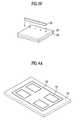
- FIG. 2Aillustrates a method of forming a seal pattern according to a screen printing method.
- a screen printing apparatusincludes a screen mask 32 having an opening 31 for selectively exposing a seal pattern region and a squeegee 33 for forming the seal pattern on the first substrate 10 by selectively providing sealant material to the first substrate 10 via the screen mask 32 .
- sealant materialis disposed and the seal pattern is formed on the first substrate 10 in regions corresponding to the opening 31 by rolling a squeegee 33 over the first substrate 10 along the arrow direction in the drawing.
- solvent within the seal patternis evaporated in a drying process for leveling.
- the seal patternincludes a liquid crystal injection inlet at one side thereof and is arranged at a periphery of a picture display region to prevent liquid crystal from leaking.
- the aforementioned related art screen printing methodis a relatively simple process to perform.
- use of the aforementioned related art screen printing methodis problematic because the amount of sealant material used can be excessive. More specifically, while sealant material is disposed over the entire surface of the screen mask 32 , only a small portion of the disposed sealant material is actually incorporated into the seal pattern by the squeegee 33 . Further, the screen mask 32 contacts the first substrate 10 . Such contact generates defects within an alignment layer (not shown) formed on the first substrate 10 because the screen mask 32 damages the alignment layer. Accordingly, a picture quality of the related art LCD device becomes deteriorated.
- FIG. 2Billustrates a method of forming a seal pattern according to a dispensing method.
- the first substrate 10i.e., the TFT array substrate
- a stagecapable of moving in many directions.
- sealant material 7is selectively dispensed along the periphery of the first substrate 10 via a syringe apparatus 34 .
- the seal pattern 7is typically divided into a main seal pattern and a dummy seal pattern wherein the dummy seal pattern is formed to protect the main seal pattern and to prevent liquid crystal material from leaking.
- a seal patternis formed along the periphery of the first substrate 10 .
- the amount of sealant material usedmay be decreased compared to the aforementioned related art screen printing method since sealant material is selectively dispensed along the periphery of the first substrate 10 . Further, the syringe apparatus 34 does not contact the first substrate 10 such that damage to the alignment layer is substantially avoided and the picture quality of the LCD device is improved.
- the present inventionis directed to a method for manufacturing a liquid crystal display device that substantially obviates one or more problems due to limitations and disadvantages of the related art.
- An advantage of the present inventionprovides a method for manufacturing a liquid crystal display device having an improved device reliability and decreased tact time.
- Another advantage of the present inventionprovides a method for manufacturing a liquid crystal display device capable of being applied to Multi-Model-on-a-Glass (MMG) models of liquid crystal display panels having various sizes.
- MMGMulti-Model-on-a-Glass
- a method for manufacturing an liquid crystal display devicemay, for example, include providing first and second substrates; forming a main sealant pattern on one of the first and second substrates via a printing method; forming a dummy sealant pattern on the substrate on which the main sealant pattern was formed via a dispensing method; dispensing liquid crystal material directly onto one of the first and second substrates; attaching the first and second substrates together; and irradiating the attached first and second substrates with UV light.
- FIG. 1illustrates a plan view illustrating a related art LCD device
- FIG. 2Aillustrates a method of forming a seal pattern according to a screen printing method
- FIG. 2Billustrates a method of forming a seal pattern according to a dispensing method
- FIGS. 3A to 3 Fillustrate process steps of manufacturing an LCD device according to the principles of the present invention
- FIGS. 4A to 4 Cillustrate dummy seal patterns according to the principles of the present invention
- FIGS. 5A to 5 Cillustrate a method of forming a main seal pattern according to a screen printing method in accordance with the principles of the present invention
- FIG. 6Aillustrates a plan view of a one piece screen mask
- FIG. 6Billustrates a plan view of a division screen mask
- FIG. 7illustrates an exemplary MMG model including a plurality of different sized LCD panels disposed within the same base substrate
- FIG. 8illustrates UV fixation of a seal pattern according to the principles of the present invention.
- FIGS. 3A to 3 Fillustrate process steps of manufacturing an LCD device according to the principles of the present invention.
- four LCD panelsmay, for example, be formed within the same base substrate.
- the number of LCD panels formed within the same substratemay be varied according to the size of the substrate.
- first and second substrates 30 and 20may be prepared as required.
- a plurality of gate lines and a plurality of data lines crossing the gate linesmay, for example, be formed on the first substrate 20 wherein a plurality of pixel regions may be defined by the crossings of the gate and data lines.
- Thin film transistors (TFTs)may be formed at crossings of the gate and data lines, wherein each TFT may include a gate electrode, a gate insulating layer, a semiconductor layer, an ohmic contact layer, source and drain electrodes, and a passivation layer.
- pixel electrodesmay be formed within respective ones of the plurality of pixel regions and may be connected to corresponding ones of the TFTs.
- an alignment layermay be formed on the pixel electrodes to impart an initial alignment direction to molecules within subsequently dispensed liquid crystal material.
- the alignment layermay be formed of a polyamide or polyimide group compound material, polyvinylalcohol (PVA), polyamic acid, and the like.
- the alignment direction of the alignment layermay provided via a rubbing process.
- the alignment layermay be formed of any material having a photoreactive group including, for example, polyvinylcinnamate (PVCN), polysiloxanecinnamate (PSCN), cellulosecinnamate (CelCN), and the like.
- the alignment direction of the alignment layermay provided via a light exposure process.
- the second substrate 30may, for example, support a black matrix layer, an R/G/B color filter layer, and a common electrode.
- the black matrix layermay substantially prevent light from leaking to the gate lines, the data lines and the TFTs.
- the R/G/B color filter layermay be formed on the black matrix layer and the common electrode may be formed on the color filter layer.
- an overcoat layermay be formed between the color filter layer and the common electrode.
- the aforementioned alignment layermay also be formed on the common electrode.
- silver (Ag) pastemay be formed at the periphery of the first substrate 20 to facilitate the application of a voltage to the common electrode of a bonded second substrate 30 .
- the first and second substrates 20 and 30may form an In-Plane Switching (IPS) mode LCD device. Therefore, both the common electrode and the pixel electrodes may be formed on the first substrate 20 to induce an in-plane electric field and formation of the silver (Ag) paste may not be necessary.
- IPSIn-Plane Switching
- the liquid crystal material 40may be dispensed directly onto the first substrate 20 , thereby forming a layer of liquid crystal material.
- a main seal pattern 70may be formed on the second substrate 30 via a screen printing method.
- a dummy seal pattern 60may be formed in a dummy region at the periphery of the second substrate 30 in a dispensing method using a dispensing apparatus 50 .
- the dummy seal pattern 60may be formed to protect the main seal pattern 70 and to maintain a vacuum state of a cell gap between the first and second substrates during a subsequent bonding process.
- the dummy seal pattern 60may be formed substantially within any portion of the dummy region of the second substrate 30 . Further, the dummy seal pattern 60 may be formed either after or before formation of the main seal pattern 70 . While it has been shown in FIG.
- the dummy seal pattern 60may be provided as a closed shape
- the principles of the present inventionmay be readily extended to provide the dummy seal pattern 60 in substantially any shape, examples of which will be described in greater detail below with reference to FIGS. 4A to 4 C.
- the main and dummy seal patterns 70 and 60may be formed out of a sealant material that hardens upon exposure to UV light. Accordingly, in one aspect of the present invention, at least one of the main and dummy seal patterns 70 and 60 may be formed out of a sealant material including monomers or oligomers each having both ends coupled with an acrylic group mixed with an initiator. In another aspect of the present invention, at least one of the main and dummy seal patterns 70 and 60 may be formed out of a selant material including or monomers or oligomers each having one end coupled with an acrylic group and the other end coupled with an epoxy group mixed with an initiator.
- the liquid crystal material 40may become contaminated. Accordingly, the liquid crystal material 40 may be dispensed at the center portion of the first substrate 20 .
- the liquid crystal material 40 dispensed at the center portion of the first substrate 20may spread over the entire surface of the substrate until the main seal pattern 70 is hardened and after the main seal pattern 70 is hardened, such that a uniform amount of liquid crystal material is provided over the entire surface of the bonded substrates.
- the liquid crystal material 40may be dispensed on a different substrate than the main and dummy seal patterns 70 and 60 .
- the liquid crystal material 40may be dispensed on the second substrate 30 while the main and dummy seal patterns 70 and 60 may be formed on the first substrate 20 .
- Forming the liquid crystal material 40 and the main and dummy seal patterns 70 and 60 on different substratesmay, however, increase the time required to manufacture the LCD because the processes required to form the main and dummy seal patterns 70 and 60 may be different from the amount of time required to dispense the liquid crystal material 40 .
- the liquid crystal material 40 and the main and dummy seal patterns 70 and 60may be formed on the same substrate.
- Forming the liquid crystal material 40 and the main and dummy seal patterns 70 and 60 on the same substratesmay make it difficult to clean the substrate because the seal patterns may be contaminated prior to bonding the two substrates together. Accordingly, and with reference to FIG. 3D, after forming the main and dummy seal patterns 70 and 60 on the second substrate 30 , the second substrate 30 may be cleaned prior to the bonding process described below.
- spacersmay be formed on any one of the first and second substrates 20 and 30 to maintaining a substantially uniform cell gap between the first and second substrates 20 and 30 .
- the spacersmay be formed on the second substrate 30 .
- the spacersmay be provided as ball-type spacers, wherein ball-type spacers may be mixed into a solution at a predetermined density. Subsequently, the solution having the mixed-in ball-type spacers may be sprayed onto the substrate via a high pressure spraying nozzle. If ball-type spacers are applied to large-sized LCD devices, it may become difficult to maintain a uniform cell gap between the first and second substrates.
- the spacersmay be provided as column-type spacers such that column-type spacers may be formed over the substrate in regions corresponding to one of the gate lines, the common line, and the data lines.
- column-type spacersmay be formed on a base substrate having large-sized LCD devices disposed therein via photolithographic processes.
- the column-type spacersmay be formed of a material such as a photosensitive organic resin (e.g., photo-acrylate, Benzocyclobutene (BCB), or polyimide, or the like).
- a photosensitive organic resine.g., photo-acrylate, Benzocyclobutene (BCB), or polyimide, or the like.
- the first and second substrates 30 and 20may be bonded together.
- the substrate onto which the liquid crystal was dispensedmay be arranged beneath the other substrate such that the surface of the substrate directly contacting the dispensed liquid crystal material 40 faces toward the other substrate.
- the substrate onto which the seal patterns are formedmay be arranged over the other substrate such that the surface of the substrate directly contacting the seal patterns faces toward the other substrate. Accordingly, the surfaces of the two substrates in direct contact with the liquid crystal material and the seal patterns oppose each other.
- the bondingmay be performed by pressing the uppermost substrate toward the lowermost substrate.
- the bondingmay be performed by releasing a vacuum state maintained between the two substrates when they are separated from each other.
- the bonded first and second substrates 20 and 30may be irradiated with UV light via a UV irradiation apparatus 80 .
- monomer or oligomer material within the seal patternsmay become polymerized by the initiator within the seal pattern and the first and second substrates 20 and 30 may be bonded together.
- the seal patternmay include monomers or oligomers each having one end coupled to the acrylic group and the other end coupled to the epoxy group mixed with the initiator, wherein the epoxy group is substantially inert to the UV light.
- the seal patternsmay be heated to a temperature of about 120° C. for about one hour after being irradiated by the UV light to harden the seal patterns.
- Irradiating the UV light irradiation to the entire surface of the bonded substratesmay affect characteristics of devices formed on the substrates (e.g., the thin film transistors) and alter pretilt angles of the alignment layers formed to initially align the liquid crystal material 40 .
- a mask(not shown) may be arranged between the UV irradiation apparatus and the bonded substrates 20 and 30 to shield active regions defined by the main seal patterns 70 .
- the bonded substratesmay be cut into individual LCD panels and an inspection process may be performed.
- the layer of liquid crystal materialmay be formed according to a liquid crystal injection method instead of the liquid crystal dispensing method. Therefore, the main and dummy seal patterns 70 and 60 may be formed within the same plane. Moreover, the dummy seal pattern may maintain a substantially uniform cell gap within a non-display (e.g., dummy) region and the main seal patterns may include liquid crystal injection inlets.
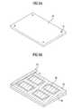
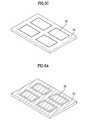
- FIGS. 4A to 4 Cillustrate dummy seal patterns according to the principles of the present invention.
- the main seal pattern 70provided as a plurality of main seal patterns 70 , may arranged on the second substrate 30 as a closed shape having no liquid crystal injection inlet while the dummy seal pattern 60 may be provided within the dummy region at the periphery of the main seal patterns 70 in substantially any shape.
- the dummy seal pattern 60may be provided at the periphery of the main seal patterns 70 in a closed shape.
- the dummy seal pattern 60may be provided as a plurality of dummy seal sub-patterns 60 arranged at corners of the second substrate 30 where the main seal pattern 70 is formed.
- the plurality of dummy seal sub-patterns 60may be provided as “L”-type shapes arranged to surround portions of respective main seal patterns 70 .
- FIG. 4Athe dummy seal pattern 60 may be provided at the periphery of the main seal patterns 70 in a closed shape.
- the dummy seal pattern 60may be provided as a plurality of dummy seal sub-patterns 60 arranged at corners of the second substrate 30 where the main seal pattern 70 is formed.
- the plurality of dummy seal sub-patterns 60may be provided as “L”-type shapes arranged to surround portions of respective main seal patterns 70 .
- the plurality of dummy seal sub-patterns 60may be provided as substantially straight-type shapes arranged at outer peripheral sides of respective ones of the main seal patterns 70 .
- the dummy seal patterns 60 shown in FIGS. 4A to 4 Cmay be formed out of a material including monomers or oligomers each having both ends coupled with an acrylic group mixed with an initiator.
- the dummy seal patterns 60 shown in FIGS. 4A to 4 Cmay be formed out of a material including monomers or oligomers each having one end coupled with an acrylic group and the other end coupled with an epoxy group mixed with an initiator.
- FIGS. 5A to 5 Cillustrate a method of forming a main seal pattern according to a screen printing method in accordance with the principles of the present invention.
- a plurality of alignment marks 31may be formed on the surface of at least one of the first and second substrates 20 and 30 , respectively, (e.g., the second substrate 30 ).
- at least two alignment marks 31may be arranged at respective corners of the second substrate 30 .
- the at least two alignment marks 31may be arranged in diagonally opposite corners of the second substrate 30 .
- four alignment marks 31may be arranged at respective corners of the second substrate 30 .
- four alignment marks 31may be arranged at corners of liquid crystal display panels within the second substrate 30 .
- the plurality of alignment marks 31may be provided as various shape-types (e.g., at least one of a +-type shape, a X-type shape, a rectangular shape, a circular shape, etc.).
- a screen mask 33may be arranged over the second substrate 30 . Further, the screen mask 33 may be provided with a plurality of openings 32 capable of being aligned over predetermined regions of the second substrate 30 using the plurality of alignment marks 31 . After aligning the screen mask 33 , a sealant material may be disposed over a predetermined portion of the screen mask 33 and a squeegee 34 may be rolled over the screen mask 33 along the arrow direction shown in FIG. 5B to force sealant material within the openings 32 . Consequently, and as shown in FIG.
- four main seal patterns 70may be formed on the second substrate 30 in correspondence to the plurality of openings 32 wherein the four main seal patterns 70 may be used to fabricate four LCD panels.
- the screen mask 33may be provided as a one piece screen mask as shown in FIG. 6A. In another aspect of the present invention, the screen mask 33 may be provided as a division screen mask as shown in FIG. 6B.
- the main seal patterns 70may be printed using a one piece screen mask 33 having a plurality of openings 32 used to a form a plurality of main seal patterns 70 .
- the size of the one piece screen maskis limited to a maximum size. Therefore, it becomes difficult to effectively use remaining portions of large-sized base substrates (i.e., portions of the base substrate within which LCD panels are not formed) and the cost of manufacturing LCD panels may be excessively large. Further, the size of the one piece screen mask must be increased in accordance with the size of the LCD panel. As the size of LCD panels increases, the size of the one piece screen mask also increases, thereby making the one piece screen mask difficult to maintain and handle.
- the main seal patterns 70may be printed using a division screen mask 33 having a single opening 32 corresponding to dimensions of an LCD panel.
- the main seal pattern 70may be arranged on the second substrate 30 corresponding the LCD panel.
- a sealant materialmay be disposed over the division screen mask 33 and the main seal pattern 70 may be printed in a region of the second substrate 30 corresponding to a first LCD panel region via a squeegee 34 (as in FIG. 5B).
- the division screen mask 33may be re-arranged in another region of the second substrate 30 corresponding to a second LCD panel region and another main seal pattern 70 may be printed on the second LCD panel region.
- the aforementioned processesmay be repeated to form a predetermined number of printed main seal patterns in regions of the second substrate corresponding to LCD panel regions.
- any number main seal patterns 70e.g., four may be printed on the within corresponding LCD panel regions of the same base substrate.
- a plurality of LCD panels having different sizesmay be formed within the same base substrate using the division screen mask 33 .
- the efficiency with which the substrate may be useddecreases.
- a plurality of different sized LCD panelse.g., a first plurality of LCD panels having a first size and a second plurality of LCD panels having a second size, smaller than the first size
- the second plurality of LCD panelsmay be formed within a remaining portion of the substrate even though the first plurality of LCD panels cannot be formed within the remaining portion.
- FIG. 7illustrates an exemplary MMG model including a plurality of different sized LCD panels disposed within the same base substrate.
- a first plurality of LCD panels 22 having a first sizemay be formed within a base substrate 21 and a second plurality of LCD panels 23 having a second size, smaller than the first size, may be formed within a remaining portion of the base substrate 21 .
- the remaining portion of the base substrate, having a size suitable for accommodating the second plurality of LCD panels 23cannot be used and the base substrate 21 is used inefficiently.
- the first and second plurality of LCD panels, having the different sizesmay be formed within the same base substrate to optimize use of the base substrate.
- the plurality of main seal patterns 70may be formed on the base substrate 21 at the periphery of first and second plurality of LCD panels 22 and 23 .
- the plurality of main seal patterns 70may be formed on the base substrate by a printing method.
- the aforementioned dummy seal pattern 60may be formed at the periphery of the main seal patterns 70 via a dispensing method wherein sealant material is selectively dispensed directly onto the base substrate 21 .
- FIG. 8illustrates UV fixation of a seal pattern according to the principles of the present invention.
- the aforementioned seal patternsmay be formed of a photo-hardening type sealant material (e.g., a UV hardening-type resin), wherein the main seal patterns 70 seal liquid crystal material between two bonded substrates within the LCD panels, and wherein the dummy seal pattern 60 surrounds the plurality of LCD panels, protects the main seal patterns 70 , and maintains a vacuum state between the substrates during the bonding and pressing processes.
- a fixation seal pattern 90may be provided at fixed intervals at a periphery of the dummy seal pattern 60 , proximate edges of the second substrate 30 .
- the fixation seal pattern 90may fix the two bonded substrates and may be removed in a subsequent cutting operation used to divide the bonded substrates into a plurality of LCD panels.
- the two substratesmay be bonded to each other. Subsequently, UV light may be irradiated to the fixation seal patterns 90 , thereby hardening the fixation seal patterns 90 . As a result, the two substrates bonded to each other are fixed.
- the main seal pattern 70 , the dummy seal pattern 60 , and the fixation seal pattern 90may be formed on the second substrate 30 .
- the fixation seal pattern 90may be formed on the first substrate.
- the fixation seal pattern 90may be formed of a different material from the main seal pattern 70 .
- the fixation seal pattern 90may be formed of the same material as the main seal pattern 70 and the fixation seal pattern 90 may be formed on the same substrate as the main seal pattern 70 (e.g., the second substrate 30 ). In still another aspect of the present invention, the fixation seal pattern 90 may be formed of the different material from the main seal pattern 70 and the fixation seal pattern 90 may be formed on a different substrate from the main seal pattern 70 or on the same substrate as the main seal pattern 70 (e.g., the second substrate 30 ). In one aspect of the present invention, the main seal pattern 70 and the liquid crystal may be formed on the first substrate 20 while the fixation seal pattern 90 may be formed on the second substrate 30 .
- the fixation seal pattern 90 and the liquid crystal materialmay be formed on the first substrate 20 , and either the main or dummy seal pattern 70 or 60 may be formed on the second substrate 30 .
- the fixation seal pattern 90may be formed via the aforementioned dispensing method whereby sealant material is selectively dispensed onto the substrate.
- the fixation seal pattern 90may be formed at the periphery of the dummy seal pattern 60 or substantially collinear with the dummy seal pattern 60 .
- the aforementioned method of manufacturing LCD devices in accordance with the present inventionis advantageous because the main seal pattern may be formed by a screen printing method and the dummy seal pattern may be formed by a dispensing method. Accordingly, contamination of the liquid crystal material may be prevented, thereby improving yield and device reliability. Further, main seal patterns may be printed onto a base substrate (e.g., a large-sized substrate) using a division screen mask or a one piece screen mask. Still further, main seal patterns corresponding to LCD panels of different sizes may be formed on the same base substrate. Moreover, a tact time may be decreased.
Landscapes
- Physics & Mathematics (AREA)
- Nonlinear Science (AREA)
- Chemical & Material Sciences (AREA)
- Crystallography & Structural Chemistry (AREA)
- General Physics & Mathematics (AREA)
- Optics & Photonics (AREA)
- Mathematical Physics (AREA)
- Liquid Crystal (AREA)
Abstract
Description
- This application claims the benefit of the Korean Application No. P2002-74819 filed on Nov. 28, 2002, which is hereby incorporated by reference for all purposes as if fully set forth herein. This application incorporates by reference two co-pending application Ser. No. 10/184,096, filed on Jun. 28, 2002, entitled “SYSTEM AND METHOD FOR MANUFACTURING LIQUID CRYSTAL DISPLAY DEVICES” (Attorney Docket Number 8733.666.00) and Ser. No. 10/184,088, filed on Jun. 28, 2002, entitled “SYSTEM FOR FABRICATING LIQUID CRYSTAL DISPLAY AND METHOD OF FABRICATING LIQUID CRYSTAL DISPLAY USING THE SAME” (Attorney Docket Number 8733.684.00), as if fully set forth herein.[0001]
- 1. Field of the Invention[0002]
- The present invention relates to a liquid crystal display (LCD) device, and more particularly, to a method for manufacturing an LCD device while decreasing a tact time.[0003]
- 2. Discussion of the Related Art[0004]
- With the expansion of the information society, a need has arisen for displays capable of producing high quality images in thin, lightweight packages and that consume little power. To meet such needs, research has produced a variety of flat panel display devices, including liquid crystal displays (LCD), plasma displays (PDP), electro luminescent displays (ELD), and vacuum fluorescent displays (VFD). Some of these display technologies have already been applied in information displays.[0005]
- Of the various types of flat panel display devices, LCDs are very widely used. In fact, in portable devices, such as notebook PC computers, LCD technology has already replaced cathode ray tubes (CRT) as the display of choice. Moreover, even in desktop PCs and in TV monitors, LCDs devices are becoming more common.[0006]
- Despite various technical developments in LCD technology, however, research in enhancing picture quality of LCD devices has been lacking compared to research in other features and advantages of LCD devices. Therefore, to increase the use of LCD devices as displays in various fields of application, LCD devices capable of expressing high quality images (e.g., images having a high resolution and a high luminance) with large-sized screens, while still maintaining a light weight, minimal dimensions, and low power consumption must be developed.[0007]
- LCDs generally include an LCD panel for displaying a picture and a driving part for providing driving signals to the liquid crystal display panel.[0008]
- Typically, LCD panels include first and second glass substrates bonded to each other while being spaced apart by a cell gap, wherein a layer of liquid crystal material is injected into the cell gap.[0009]
- The first glass substrate (i.e., thin film transistor (TFT) array substrate), supports a plurality of gate lines spaced apart from each other at a fixed interval and extending along a first direction; a plurality of data lines spaced apart from each other at a fixed interval and extending along a second direction, substantially perpendicular to the first direction, wherein pixel regions are defined by crossings of the gate and data lines; a plurality of pixel electrodes arranged in a matrix pattern within respective ones of the pixel regions; and a plurality of thin film transistors (TFTs) capable of transmitting signal from the data lines to corresponding ones of the pixel electrodes in response to a signal applied to respective ones of the gate lines.[0010]
- The second glass substrate (i.e., color filter substrate) supports a black matrix layer for preventing light leakage in areas outside the pixel regions; a color filter layer (R, G, B) for selectively transmitting light having predetermined wavelengths; and a common electrode for displaying a picture. Common electrodes of In-Plane Switching (IPS) mode LCD devices, however, are formed on the first substrate.[0011]
- Uniformity of the cell gap is maintained by spacers arranged between the first and second glass substrates, bonded together by a seal pattern. The seal pattern includes a liquid crystal injection inlet allowing liquid crystal material to be injected into the cell gap. Upon injecting liquid crystal material into the cell gap via the liquid crystal injection inlet, the layer of liquid crystal material is thus formed.[0012]
- The layer of liquid crystal material is driven (e.g., light transmittance characteristics of the layer of liquid crystal material are controlled) according to electric fields generated between the first and second substrates by the pixel electrode and the common electrode. By controlling the light transmittance characteristics of the layer of liquid crystal material, pictures may be displayed.[0013]
- To form the aforementioned layer of liquid crystal material, related art manufacturing methods incorporate a liquid crystal injection method wherein a pressure difference is created between the cell gap and a vacuum chamber and liquid crystal material is injected into the liquid crystal injection inlet via a capillary phenomenon. A method for manufacturing the related art LCD device incorporating the liquid crystal injection method will now be described.[0014]
- The first substrate (i.e., a TFT array substrate), supporting the TFTs and pixel electrodes, and the second substrate (i.e., the color filter substrate), supporting the black matrix layer, color filter layer, and common electrode, are provided. Next, spacers are dispersed on the TFT array substrate to maintain a uniform cell gap between the two substrates. A seal pattern is then formed at a periphery of the other of the two substrates to prevent liquid crystal material from leaking and to bond the two substrates together. The seal pattern is typically formed of a thermo-hardening material such as an epoxy including a mixture of an epoxy resin and an initiator. Next, a heat treatment is performed to bond the TFT array and color filter substrates to each other. When performing the heat treatment, the epoxy resin within the epoxy seal pattern is activated by the initiator and becomes a highly cross-linked polymer. As a result, the epoxy seal pattern functions as the seal pattern having suitable adhesion characteristics.[0015]
- Subsequently, the bonded substrates are placed in a vacuum chamber, wherein the cell gap between the bonded substrates is maintained in a vacuum state, and dipped into a reservoir of liquid crystal material. Since a vacuum is maintained within the cell gap, liquid crystal material is injected into the cell gap by a capillary phenomenon. After a predetermined amount of liquid crystal material has been injected into the cell gap, nitrogen gas (N[0016]2) is pumped into the vacuum chamber, so that liquid crystal material is injected into regions of the cell gap not previously injected into, according to the pressure difference between the cell gap and the pressure within the vacuum chamber having the pumped nitrogen gas (N2). As a result, the layer of liquid crystal material is formed between the bonded TFT array and color filter substrates.
- FIG. 1 illustrates a plan view illustrating a related art LCD device.[0017]
- Referring to FIG. 1, the first substrate (i.e., the TFT array substrate) supports a plurality of[0018]
gate lines 11 spaced apart from each other at a fixed interval and extending along a first direction and a plurality ofdata lines 12 spaced apart from each other at a fixed interval and extending along a second direction, substantially perpendicular to the first direction. Pixel regions P are defined by crossings of the gate anddata lines pixel electrodes 16 are arranged in a matrix pattern within respective ones of the pixel regions P, and thin film transistors are formed at crossings of the plurality of gate anddata lines gate lines 11, the thin film transistors transmit signals applied from thedata lines 12 to respective ones of thepixel electrodes 16. - Each the thin film transistor includes a[0019]
gate electrode 13 protruding from acorresponding gate line 11, a gate insulating layer (not shown) formed over an entire surface of thefirst substrate 10, a semiconductor layer15 formed on the gate insulating layer in a region above thegate electrode 13, asource electrode 15aprotruding from acorresponding data line 12, and adrain electrode 15bformed opposite thesource electrode 15aby a predetermined distance and electrically connected to thepixel electrode 16 through acontact hole 17. - The second substrate (i.e., the color filter substrate; not shown) supports a black matrix layer having openings in regions corresponding to the pixel regions P of the[0020]
first substrate 10 and prevents light leakage; an R/G/B color filter layer for selectively transmitting light having predetermined wavelengths; and a common electrode for driving the layer of liquid crystal material with thepixel electrodes 16. - The[0021]
first substrate 10 is bonded to the second substrate (i.e., the color filter substrate), wherein the two substrates are spaced apart from each other by a predetermined distance, uniformly maintained by spacers. The first and second substrates are bonded to each other using a seal pattern having a liquid crystal injection inlet. Upon injecting liquid crystal material into the cell gap via the liquid crystal injection inlet, the layer of liquid crystal material is thus formed. - FIG. 2A illustrates a method of forming a seal pattern according to a screen printing method.[0022]
- Referring to FIG. 2A, a screen printing apparatus includes a[0023]
screen mask 32 having anopening 31 for selectively exposing a seal pattern region and asqueegee 33 for forming the seal pattern on thefirst substrate 10 by selectively providing sealant material to thefirst substrate 10 via thescreen mask 32. After arranging thescreen mask 32 on thefirst substrate 10, sealant material is disposed and the seal pattern is formed on thefirst substrate 10 in regions corresponding to theopening 31 by rolling asqueegee 33 over thefirst substrate 10 along the arrow direction in the drawing. Next, solvent within the seal pattern is evaporated in a drying process for leveling. Further, the seal pattern includes a liquid crystal injection inlet at one side thereof and is arranged at a periphery of a picture display region to prevent liquid crystal from leaking. - The aforementioned related art screen printing method is a relatively simple process to perform. However, use of the aforementioned related art screen printing method is problematic because the amount of sealant material used can be excessive. More specifically, while sealant material is disposed over the entire surface of the[0024]
screen mask 32, only a small portion of the disposed sealant material is actually incorporated into the seal pattern by thesqueegee 33. Further, thescreen mask 32 contacts thefirst substrate 10. Such contact generates defects within an alignment layer (not shown) formed on thefirst substrate 10 because thescreen mask 32 damages the alignment layer. Accordingly, a picture quality of the related art LCD device becomes deteriorated. - In order to solve the problems arising from use of the aforementioned related art screen printing method, a seal dispensing method has been proposed.[0025]
- FIG. 2B illustrates a method of forming a seal pattern according to a dispensing method.[0026]
- Referring to FIG. 2B, the first substrate[0027]10 (i.e., the TFT array substrate) is loaded onto a stage (not shown) capable of moving in many directions. Next, sealant material7 is selectively dispensed along the periphery of the
first substrate 10 via asyringe apparatus 34. Though not shown in FIG. 2B (or2A), the seal pattern7 is typically divided into a main seal pattern and a dummy seal pattern wherein the dummy seal pattern is formed to protect the main seal pattern and to prevent liquid crystal material from leaking. Upon selectively dispensing sealant material along the periphery of thefirst substrate 10, a seal pattern is formed along the periphery of thefirst substrate 10. Using the aforementioned related art dispensing method, the amount of sealant material used may be decreased compared to the aforementioned related art screen printing method since sealant material is selectively dispensed along the periphery of thefirst substrate 10. Further, thesyringe apparatus 34 does not contact thefirst substrate 10 such that damage to the alignment layer is substantially avoided and the picture quality of the LCD device is improved. - Use of the aforementioned related art dispensing method of forming the seal pattern is problematic, however, because the main and dummy seal patterns are formed of highly viscous sealant material. Accordingly, a nozzle of the[0028]
syringe apparatus 34 becomes sticky with sealant material and an excessive amount of sealant material is accumulated on the nozzle. Subsequently, the excessive amount of sealant material accumulated on the nozzle becomes excessively dispensed onto the first substrate. During bonding of the first and second substrates, the excessively dispensed sealant material spreads toward an active region (center portion of the first substrate) and a dummy region (periphery of the first substrate) and the liquid crystal material becomes contaminated by the sealant material, thereby decreasing device reliability. - Further, use of the related art seal pattern formation methods may become difficult when the size of the first substrate increases, or when a size of the picture display area of the substrate changes (e.g., upon a model change of the liquid crystal display panel). In light of recent demand for liquid crystal display panels having increased size, the size of the first substrate has increased. Accordingly, positions where seal patterns are formed on the substrate change.[0029]
- In the aforementioned related art dispensing method, if the positions where the seal pattern is formed on the substrate changes, the syringe apparatus must be disassembled and reassembled. As the size of liquid crystal display panels increase, the amount of time required to dispense a seal pattern having an increased size also increases. Accordingly, the tact time increases and the yield decreases.[0030]
- Accordingly, the present invention is directed to a method for manufacturing a liquid crystal display device that substantially obviates one or more problems due to limitations and disadvantages of the related art.[0031]
- An advantage of the present invention provides a method for manufacturing a liquid crystal display device having an improved device reliability and decreased tact time.[0032]
- Another advantage of the present invention provides a method for manufacturing a liquid crystal display device capable of being applied to Multi-Model-on-a-Glass (MMG) models of liquid crystal display panels having various sizes.[0033]
- Additional features and advantages of the invention will be set forth in the description which follows, and in part will be apparent from the description, or may be learned by practice of the invention. These and other advantages of the invention will be realized and attained by the structure particularly pointed out in the written description and claims hereof as well as the appended drawings.[0034]
- To achieve these and other advantages and in accordance with the purpose of the invention, as embodied and broadly described herein, a method for manufacturing an liquid crystal display device may, for example, include providing first and second substrates; forming a main sealant pattern on one of the first and second substrates via a printing method; forming a dummy sealant pattern on the substrate on which the main sealant pattern was formed via a dispensing method; dispensing liquid crystal material directly onto one of the first and second substrates; attaching the first and second substrates together; and irradiating the attached first and second substrates with UV light.[0035]
- It is to be understood that both the foregoing general description and the following detailed description of the present invention are exemplary and explanatory and are intended to provide further explanation of the invention as claimed.[0036]
- The accompanying drawings, which are included to provide a further understanding of the invention and are incorporated in and constitute a part of this application, illustrate embodiment(s) of the invention and together with the description serve to explain the principle of the invention.[0037]
- In the drawings:[0038]
- FIG. 1 illustrates a plan view illustrating a related art LCD device;[0039]
- FIG. 2A illustrates a method of forming a seal pattern according to a screen printing method;[0040]
- FIG. 2B illustrates a method of forming a seal pattern according to a dispensing method;[0041]
- FIGS. 3A to[0042]3F illustrate process steps of manufacturing an LCD device according to the principles of the present invention;
- FIGS. 4A to[0043]4C illustrate dummy seal patterns according to the principles of the present invention;
- FIGS. 5A to[0044]5C illustrate a method of forming a main seal pattern according to a screen printing method in accordance with the principles of the present invention;
- FIG. 6A illustrates a plan view of a one piece screen mask;[0045]
- FIG. 6B illustrates a plan view of a division screen mask;[0046]
- FIG. 7 illustrates an exemplary MMG model including a plurality of different sized LCD panels disposed within the same base substrate; and[0047]
- FIG. 8 illustrates UV fixation of a seal pattern according to the principles of the present invention.[0048]
- Reference will now be made in detail to the exemplary embodiments of the present invention, examples of which are illustrated in the accompanying drawings. Wherever possible, the same reference numbers will be used throughout the drawings to refer to the same or like parts.[0049]
- As sizes of liquid crystal display panels increase, the related art method of manufacturing LCD devices incorporating the liquid crystal injection method has become problematic. More specifically, the amount of time required to completely inject liquid crystal material between two substrates increases as the size of the LCD panel increases. Accordingly, the yield with which LCD devices are manufactured decrease. In order to solve the aforementioned problem, a liquid crystal dispensing method has been proposed in accordance with the principles of the present invention.[0050]
- A method for manufacturing LCD devices using the aforementioned liquid crystal dispensing method will now be described in greater detail.[0051]
- FIGS. 3A to[0052]3F illustrate process steps of manufacturing an LCD device according to the principles of the present invention.
- Referring to FIGS. 3A to[0053]3F, four LCD panels may, for example, be formed within the same base substrate. In one aspect of the present invention, the number of LCD panels formed within the same substrate may be varied according to the size of the substrate.
- As shown in FIG. 3A, first and[0054]
second substrates first substrate 20 wherein a plurality of pixel regions may be defined by the crossings of the gate and data lines. Thin film transistors (TFTs) may be formed at crossings of the gate and data lines, wherein each TFT may include a gate electrode, a gate insulating layer, a semiconductor layer, an ohmic contact layer, source and drain electrodes, and a passivation layer. Further, pixel electrodes may be formed within respective ones of the plurality of pixel regions and may be connected to corresponding ones of the TFTs. - In one aspect of the present invention, an alignment layer may be formed on the pixel electrodes to impart an initial alignment direction to molecules within subsequently dispensed liquid crystal material. In one aspect of the present invention, the alignment layer may be formed of a polyamide or polyimide group compound material, polyvinylalcohol (PVA), polyamic acid, and the like. In another aspect of the present invention, the alignment direction of the alignment layer may provided via a rubbing process. In one aspect of the present invention, the alignment layer may be formed of any material having a photoreactive group including, for example, polyvinylcinnamate (PVCN), polysiloxanecinnamate (PSCN), cellulosecinnamate (CelCN), and the like. In another aspect of the present invention, the alignment direction of the alignment layer may provided via a light exposure process.[0055]
- Although not shown, the[0056]
second substrate 30 may, for example, support a black matrix layer, an R/G/B color filter layer, and a common electrode. The black matrix layer may substantially prevent light from leaking to the gate lines, the data lines and the TFTs. The R/G/B color filter layer may be formed on the black matrix layer and the common electrode may be formed on the color filter layer. In one aspect of the present invention, an overcoat layer may be formed between the color filter layer and the common electrode. In one aspect of the present invention, the aforementioned alignment layer may also be formed on the common electrode. - According to the principles of the present invention, silver (Ag) paste may be formed at the periphery of the[0057]
first substrate 20 to facilitate the application of a voltage to the common electrode of a bondedsecond substrate 30. In one aspect of the present invention, the first andsecond substrates first substrate 20 to induce an in-plane electric field and formation of the silver (Ag) paste may not be necessary. - As shown in FIG. 3B, the[0058]
liquid crystal material 40 may be dispensed directly onto thefirst substrate 20, thereby forming a layer of liquid crystal material. Subsequently, as shown in FIG. 3C, amain seal pattern 70 may be formed on thesecond substrate 30 via a screen printing method. - Referring to FIG. 3D, a[0059]
dummy seal pattern 60 may be formed in a dummy region at the periphery of thesecond substrate 30 in a dispensing method using adispensing apparatus 50. In one aspect of the present invention, thedummy seal pattern 60 may be formed to protect themain seal pattern 70 and to maintain a vacuum state of a cell gap between the first and second substrates during a subsequent bonding process. In another aspect of the present invention, thedummy seal pattern 60 may be formed substantially within any portion of the dummy region of thesecond substrate 30. Further, thedummy seal pattern 60 may be formed either after or before formation of themain seal pattern 70. While it has been shown in FIG. 3D that thedummy seal pattern 60 may be provided as a closed shape, the principles of the present invention may be readily extended to provide thedummy seal pattern 60 in substantially any shape, examples of which will be described in greater detail below with reference to FIGS. 4A to4C. - According to the principles of the present invention, the main and[0060]
dummy seal patterns dummy seal patterns dummy seal patterns - As mentioned above, when the[0061]
main seal pattern 70 contacts with theliquid crystal material 40 before hardening, theliquid crystal material 40 may become contaminated. Accordingly, theliquid crystal material 40 may be dispensed at the center portion of thefirst substrate 20. Theliquid crystal material 40 dispensed at the center portion of thefirst substrate 20 may spread over the entire surface of the substrate until themain seal pattern 70 is hardened and after themain seal pattern 70 is hardened, such that a uniform amount of liquid crystal material is provided over the entire surface of the bonded substrates. In one aspect of the present invention, theliquid crystal material 40 may be dispensed on a different substrate than the main anddummy seal patterns liquid crystal material 40 may be dispensed on thesecond substrate 30 while the main anddummy seal patterns first substrate 20. Forming theliquid crystal material 40 and the main anddummy seal patterns dummy seal patterns liquid crystal material 40. Accordingly, in another aspect of the present invention, theliquid crystal material 40 and the main anddummy seal patterns liquid crystal material 40 and the main anddummy seal patterns dummy seal patterns second substrate 30, thesecond substrate 30 may be cleaned prior to the bonding process described below. - Although not shown, spacers may be formed on any one of the first and[0062]
second substrates second substrates second substrate 30. In another aspect of the present invention, the spacers may be provided as ball-type spacers, wherein ball-type spacers may be mixed into a solution at a predetermined density. Subsequently, the solution having the mixed-in ball-type spacers may be sprayed onto the substrate via a high pressure spraying nozzle. If ball-type spacers are applied to large-sized LCD devices, it may become difficult to maintain a uniform cell gap between the first and second substrates. Therefore, and in accordance with another aspect of the present invention, the spacers may be provided as column-type spacers such that column-type spacers may be formed over the substrate in regions corresponding to one of the gate lines, the common line, and the data lines. In one aspect of the present invention, column-type spacers may be formed on a base substrate having large-sized LCD devices disposed therein via photolithographic processes. In another aspect of the present invention the column-type spacers may be formed of a material such as a photosensitive organic resin (e.g., photo-acrylate, Benzocyclobutene (BCB), or polyimide, or the like). - As shown in FIG. 3E, the first and[0063]
second substrates liquid crystal material 40 faces toward the other substrate. The substrate onto which the seal patterns are formed may be arranged over the other substrate such that the surface of the substrate directly contacting the seal patterns faces toward the other substrate. Accordingly, the surfaces of the two substrates in direct contact with the liquid crystal material and the seal patterns oppose each other. In one aspect of the present invention, the bonding may be performed by pressing the uppermost substrate toward the lowermost substrate. In another aspect of the present invention, the bonding may be performed by releasing a vacuum state maintained between the two substrates when they are separated from each other. - As shown in FIG. 3F, the bonded first and[0064]
second substrates UV irradiation apparatus 80. Upon irradiating the UV light, monomer or oligomer material within the seal patterns may become polymerized by the initiator within the seal pattern and the first andsecond substrates - Irradiating the UV light irradiation to the entire surface of the bonded substrates may affect characteristics of devices formed on the substrates (e.g., the thin film transistors) and alter pretilt angles of the alignment layers formed to initially align the[0065]
liquid crystal material 40. In one aspect of the present invention, a mask (not shown) may be arranged between the UV irradiation apparatus and the bondedsubstrates main seal patterns 70. Although not shown, after the aforementioned UV irradiation process, the bonded substrates may be cut into individual LCD panels and an inspection process may be performed. - According to the principles of the present invention, the layer of liquid crystal material may be formed according to a liquid crystal injection method instead of the liquid crystal dispensing method. Therefore, the main and[0066]
dummy seal patterns - FIGS. 4A to[0067]4C illustrate dummy seal patterns according to the principles of the present invention.
- Referring to FIGS. 4A to[0068]4C, the
main seal pattern 70, provided as a plurality ofmain seal patterns 70, may arranged on thesecond substrate 30 as a closed shape having no liquid crystal injection inlet while thedummy seal pattern 60 may be provided within the dummy region at the periphery of themain seal patterns 70 in substantially any shape. - Referring specifically to FIG. 4A, the[0069]
dummy seal pattern 60 may be provided at the periphery of themain seal patterns 70 in a closed shape. Alternatively, and while referring to FIG. 4B, thedummy seal pattern 60 may be provided as a plurality of dummy seal sub-patterns60 arranged at corners of thesecond substrate 30 where themain seal pattern 70 is formed. In one aspect of the present invention, the plurality ofdummy seal sub-patterns 60 may be provided as “L”-type shapes arranged to surround portions of respectivemain seal patterns 70. Alternatively, and while referring to FIG. 4C, the plurality ofdummy seal sub-patterns 60 may be provided as substantially straight-type shapes arranged at outer peripheral sides of respective ones of themain seal patterns 70. In one aspect of the present invention, thedummy seal patterns 60 shown in FIGS. 4A to4C may be formed out of a material including monomers or oligomers each having both ends coupled with an acrylic group mixed with an initiator. In another aspect of the present invention, thedummy seal patterns 60 shown in FIGS. 4A to4C may be formed out of a material including monomers or oligomers each having one end coupled with an acrylic group and the other end coupled with an epoxy group mixed with an initiator. - FIGS. 5A to[0070]5C illustrate a method of forming a main seal pattern according to a screen printing method in accordance with the principles of the present invention.
- Referring to FIG. 5A, a plurality of alignment marks[0071]31 may be formed on the surface of at least one of the first and
second substrates second substrate 30. In another aspect of the present invention, the at least two alignment marks31 may be arranged in diagonally opposite corners of thesecond substrate 30. In another aspect of the present invention, fouralignment marks 31 may be arranged at respective corners of thesecond substrate 30. In yet another aspect of the present invention, fouralignment marks 31 may be arranged at corners of liquid crystal display panels within thesecond substrate 30. In still another aspect of the present invention, the plurality of alignment marks31 may be provided as various shape-types (e.g., at least one of a +-type shape, a X-type shape, a rectangular shape, a circular shape, etc.). - Referring to FIG. 5B, a[0072]
screen mask 33 may be arranged over thesecond substrate 30. Further, thescreen mask 33 may be provided with a plurality ofopenings 32 capable of being aligned over predetermined regions of thesecond substrate 30 using the plurality of alignment marks31. After aligning thescreen mask 33, a sealant material may be disposed over a predetermined portion of thescreen mask 33 and asqueegee 34 may be rolled over thescreen mask 33 along the arrow direction shown in FIG. 5B to force sealant material within theopenings 32. Consequently, and as shown in FIG. 5C, fourmain seal patterns 70 may be formed on thesecond substrate 30 in correspondence to the plurality ofopenings 32 wherein the fourmain seal patterns 70 may be used to fabricate four LCD panels. In one aspect of the present invention, thescreen mask 33 may be provided as a one piece screen mask as shown in FIG. 6A. In another aspect of the present invention, thescreen mask 33 may be provided as a division screen mask as shown in FIG. 6B. - Referring to FIG. 6A, upon forming the[0073]
main seal patterns 70 corresponding to the four LCD panels, themain seal patterns 70 may be printed using a onepiece screen mask 33 having a plurality ofopenings 32 used to a form a plurality ofmain seal patterns 70. According to the principles of the present invention, the size of the one piece screen mask is limited to a maximum size. Therefore, it becomes difficult to effectively use remaining portions of large-sized base substrates (i.e., portions of the base substrate within which LCD panels are not formed) and the cost of manufacturing LCD panels may be excessively large. Further, the size of the one piece screen mask must be increased in accordance with the size of the LCD panel. As the size of LCD panels increases, the size of the one piece screen mask also increases, thereby making the one piece screen mask difficult to maintain and handle. - Referring to FIG. 6B, upon forming the[0074]
main seal patterns 70 corresponding to the four LCD panels, the main seal patterns may be printed using adivision screen mask 33 having asingle opening 32 corresponding to dimensions of an LCD panel. According to the principles of the present invention, themain seal pattern 70 may be arranged on thesecond substrate 30 corresponding the LCD panel. Subsequently, a sealant material may be disposed over thedivision screen mask 33 and themain seal pattern 70 may be printed in a region of thesecond substrate 30 corresponding to a first LCD panel region via a squeegee34 (as in FIG. 5B). Next, thedivision screen mask 33 may be re-arranged in another region of thesecond substrate 30 corresponding to a second LCD panel region and anothermain seal pattern 70 may be printed on the second LCD panel region. By providing thescreen mask 33 as a division screen mask, the aforementioned processes may be repeated to form a predetermined number of printed main seal patterns in regions of the second substrate corresponding to LCD panel regions. As a result, any number main seal patterns70 (e.g., four) may be printed on the within corresponding LCD panel regions of the same base substrate. - According to the principles of the present invention, a plurality of LCD panels having different sizes may be formed within the same base substrate using the[0075]
division screen mask 33. When forming a plurality of LCD panels having substantially the same size within the same substrate, it becomes difficult to efficiently use remaining portions of the base substrate since the size of the remaining portion of the base substrate is typically smaller than the size of the LCD panels that are formed. Accordingly, the efficiency with which the substrate may be used decreases. However, when a plurality of different sized LCD panels (e.g., a first plurality of LCD panels having a first size and a second plurality of LCD panels having a second size, smaller than the first size) are formed within the same base substrate, the efficiency with which the base substrate is used increases. In one aspect of the present invention, the second plurality of LCD panels may be formed within a remaining portion of the substrate even though the first plurality of LCD panels cannot be formed within the remaining portion. - A method for fabricating a plurality of different sized LCD panels in accordance with the principles of the present invention will now be described in greater detail below.[0076]
- FIG. 7 illustrates an exemplary MMG model including a plurality of different sized LCD panels disposed within the same base substrate.[0077]
- Referring to FIG. 7, a first plurality of LCD panels[0078]22 having a first size may be formed within a
base substrate 21 and a second plurality ofLCD panels 23 having a second size, smaller than the first size, may be formed within a remaining portion of thebase substrate 21. According to the principles of the present invention, when only the first plurality of LCD panels22 are formed within thebase substrate 21, the remaining portion of the base substrate, having a size suitable for accommodating the second plurality ofLCD panels 23 cannot be used and thebase substrate 21 is used inefficiently. Accordingly, the first and second plurality of LCD panels, having the different sizes, may be formed within the same base substrate to optimize use of the base substrate. Subsequently, the plurality ofmain seal patterns 70 may be formed on thebase substrate 21 at the periphery of first and second plurality ofLCD panels 22 and23. In one aspect of the present invention, the plurality ofmain seal patterns 70 may be formed on the base substrate by a printing method. Next, the aforementioneddummy seal pattern 60 may be formed at the periphery of themain seal patterns 70 via a dispensing method wherein sealant material is selectively dispensed directly onto thebase substrate 21. - FIG. 8 illustrates UV fixation of a seal pattern according to the principles of the present invention.[0079]
- Referring to FIG. 8, the aforementioned seal patterns may be formed of a photo-hardening type sealant material (e.g., a UV hardening-type resin), wherein the[0080]
main seal patterns 70 seal liquid crystal material between two bonded substrates within the LCD panels, and wherein thedummy seal pattern 60 surrounds the plurality of LCD panels, protects themain seal patterns 70, and maintains a vacuum state between the substrates during the bonding and pressing processes. In one aspect of the present invention, afixation seal pattern 90 may be provided at fixed intervals at a periphery of thedummy seal pattern 60, proximate edges of thesecond substrate 30. In another aspect of the present invention, thefixation seal pattern 90 may fix the two bonded substrates and may be removed in a subsequent cutting operation used to divide the bonded substrates into a plurality of LCD panels. - After forming the[0081]
fixation seal patterns 90, the two substrates may be bonded to each other. Subsequently, UV light may be irradiated to thefixation seal patterns 90, thereby hardening thefixation seal patterns 90. As a result, the two substrates bonded to each other are fixed. In one aspect of the present invention, themain seal pattern 70, thedummy seal pattern 60, and thefixation seal pattern 90 may be formed on thesecond substrate 30. In another aspect of the present invention, thefixation seal pattern 90 may be formed on the first substrate. In still another aspect of the present invention, thefixation seal pattern 90 may be formed of a different material from themain seal pattern 70. In yet another aspect of the present invention, thefixation seal pattern 90 may be formed of the same material as themain seal pattern 70 and thefixation seal pattern 90 may be formed on the same substrate as the main seal pattern70 (e.g., the second substrate30). In still another aspect of the present invention, thefixation seal pattern 90 may be formed of the different material from themain seal pattern 70 and thefixation seal pattern 90 may be formed on a different substrate from themain seal pattern 70 or on the same substrate as the main seal pattern70 (e.g., the second substrate30). In one aspect of the present invention, themain seal pattern 70 and the liquid crystal may be formed on thefirst substrate 20 while thefixation seal pattern 90 may be formed on thesecond substrate 30. In another aspect of the present invention, thefixation seal pattern 90 and the liquid crystal material may be formed on thefirst substrate 20, and either the main ordummy seal pattern second substrate 30. In still another aspect of the present invention, thefixation seal pattern 90 may be formed via the aforementioned dispensing method whereby sealant material is selectively dispensed onto the substrate. In yet another aspect of the present invention, thefixation seal pattern 90 may be formed at the periphery of thedummy seal pattern 60 or substantially collinear with thedummy seal pattern 60. - The aforementioned method of manufacturing LCD devices in accordance with the present invention is advantageous because the main seal pattern may be formed by a screen printing method and the dummy seal pattern may be formed by a dispensing method. Accordingly, contamination of the liquid crystal material may be prevented, thereby improving yield and device reliability. Further, main seal patterns may be printed onto a base substrate (e.g., a large-sized substrate) using a division screen mask or a one piece screen mask. Still further, main seal patterns corresponding to LCD panels of different sizes may be formed on the same base substrate. Moreover, a tact time may be decreased.[0082]
- It will be apparent to those skilled in the art that various modifications and variations can be made in the present invention. Thus, it is intended that the present invention covers the modifications and variations of this invention provided they come within the scope of the appended claims and their equivalents.[0083]
Claims (51)
Priority Applications (1)
| Application Number | Priority Date | Filing Date | Title |
|---|---|---|---|
| US11/441,133US7567336B2 (en) | 2002-11-28 | 2006-05-26 | Method for manufacturing liquid crystal display device |
Applications Claiming Priority (3)
| Application Number | Priority Date | Filing Date | Title |
|---|---|---|---|
| KR1020020074819AKR100710163B1 (en) | 2002-11-28 | 2002-11-28 | method for manufacturing of LCD |
| KR2002-0074819 | 2002-11-28 | ||
| KR10-2002-0074819 | 2002-11-28 |
Related Child Applications (1)
| Application Number | Title | Priority Date | Filing Date |
|---|---|---|---|
| US11/441,133DivisionUS7567336B2 (en) | 2002-11-28 | 2006-05-26 | Method for manufacturing liquid crystal display device |
Publications (2)
| Publication Number | Publication Date |
|---|---|
| US20040105065A1true US20040105065A1 (en) | 2004-06-03 |
| US7075611B2 US7075611B2 (en) | 2006-07-11 |
Family
ID=32388252
Family Applications (2)
| Application Number | Title | Priority Date | Filing Date |
|---|---|---|---|
| US10/608,371Expired - LifetimeUS7075611B2 (en) | 2002-11-28 | 2003-06-30 | LCD manufacturing method involving forming a main seal pattern by screen printing and a dummy seal pattern by selective dispensing |
| US11/441,133Expired - LifetimeUS7567336B2 (en) | 2002-11-28 | 2006-05-26 | Method for manufacturing liquid crystal display device |
Family Applications After (1)
| Application Number | Title | Priority Date | Filing Date |
|---|---|---|---|
| US11/441,133Expired - LifetimeUS7567336B2 (en) | 2002-11-28 | 2006-05-26 | Method for manufacturing liquid crystal display device |
Country Status (5)
| Country | Link |
|---|---|
| US (2) | US7075611B2 (en) |
| JP (1) | JP4094528B2 (en) |
| KR (1) | KR100710163B1 (en) |
| CN (1) | CN100401169C (en) |
| TW (1) | TWI307432B (en) |
Cited By (15)
| Publication number | Priority date | Publication date | Assignee | Title |
|---|---|---|---|---|
| US20050068488A1 (en)* | 2003-09-30 | 2005-03-31 | International Business Machines Corporation | Method of manufacturing a liquid crystal display panel |
| US20060028607A1 (en)* | 2004-08-03 | 2006-02-09 | Arima Computer Corporation | Method for fabricating an LC panel |
| US20060132696A1 (en)* | 2004-12-17 | 2006-06-22 | Au Optronics Corp. | Liquid crystal display |
| US20070091238A1 (en)* | 2005-10-26 | 2007-04-26 | Ki Chul Shin | Liquid crystal panel, print mask to print alignment layer and method for making the alignment layer |
| US20070114909A1 (en)* | 2005-11-18 | 2007-05-24 | Park Jin-Woo | Method of manufacturing flat panel display device, flat panel display device, and panel of flat panel display device |
| US20070154640A1 (en)* | 2005-12-29 | 2007-07-05 | Lee Hong S | Apparatus and method for forming seal pattern of flat panel display device |
| US20100182560A1 (en)* | 2007-07-05 | 2010-07-22 | Sharp Kabushiki Kaisha | Method for repairing glass substrate, process for producing glass substrate, glass substrate, and flat panel display |
| US20100243157A1 (en)* | 2005-12-29 | 2010-09-30 | Hae Joon Son | Sealant Forming Apparatus, Sealant Forming Method, And Method Of Manufacturing Liquid Crystal Display Device Using The Same |
| US20110300781A1 (en)* | 2010-06-08 | 2011-12-08 | Toshiba Mobile Display Co., Ltd. | Method of manufacturing liquid crystal display device |
| US20110297645A1 (en)* | 2010-06-08 | 2011-12-08 | Toshiba Mobile Display Co., Ltd. | Method of manufacturing liquid crystal display device |
| US20150179685A1 (en)* | 2013-09-24 | 2015-06-25 | Shenzhen China Star Optoelectronics Technology Co. Ltd. | Assembling Method for Array Substrate and Color Filter Substrate of Liquid Crystal Display |
| CN105974638A (en)* | 2016-07-26 | 2016-09-28 | 京东方科技集团股份有限公司 | Display substrate and display device |
| US20200065049A1 (en)* | 2008-01-04 | 2020-02-27 | Nanolumens Acquisition, Inc. | Display System and Methods |
| US20200103689A1 (en)* | 2018-09-30 | 2020-04-02 | HKC Corporation Limited | Display panel and a display device |
| US20210078294A1 (en)* | 2019-09-16 | 2021-03-18 | Shenzhenshi Yuzhan Precision Technology Co., Ltd. | Glass article, methods for manufacturing the same, and laser welding equipemnt |
Families Citing this family (25)
| Publication number | Priority date | Publication date | Assignee | Title |
|---|---|---|---|---|
| KR100755645B1 (en)* | 2000-12-29 | 2007-09-04 | 엘지.필립스 엘시디 주식회사 | LCD and its manufacturing method |
| KR100710163B1 (en)* | 2002-11-28 | 2007-04-20 | 엘지.필립스 엘시디 주식회사 | method for manufacturing of LCD |
| KR100672252B1 (en)* | 2004-06-30 | 2007-01-24 | 엘지.필립스 엘시디 주식회사 | Liquid crystal dropping device and liquid crystal dropping method |
| JP4635552B2 (en)* | 2004-10-18 | 2011-02-23 | ウシオ電機株式会社 | Display panel bonding equipment |
| KR20060034372A (en)* | 2004-10-19 | 2006-04-24 | 엘지.필립스 엘시디 주식회사 | Fail turn for liquid crystal display and manufacturing process |
| KR101074389B1 (en)* | 2004-11-05 | 2011-10-17 | 엘지디스플레이 주식회사 | method for etching thin film and method for manufacturing of liquid crystal display device using the same |
| US7948586B2 (en)* | 2005-07-11 | 2011-05-24 | Sharp Kabushiki Kaisha | Liquid crystal display device and manufacturing method thereof |
| JP4488435B2 (en)* | 2005-09-28 | 2010-06-23 | エルジー ディスプレイ カンパニー リミテッド | Manufacturing method of liquid crystal display element |
| CN100454090C (en)* | 2005-10-19 | 2009-01-21 | 统宝光电股份有限公司 | Method for manufacturing liquid crystal display panel |
| TWI349130B (en)* | 2006-05-12 | 2011-09-21 | Chimei Innolux Corp | Liquid crystal panel |
| TWI311216B (en)* | 2006-07-14 | 2009-06-21 | Innolux Display Corp | Panel used in liquid crystal display device |
| TWI392916B (en)* | 2008-07-18 | 2013-04-11 | Chimei Innolux Corp | Liquid crystal display panel, manufacturing method thereof and liquid crystal display |
| JP5351287B2 (en)* | 2010-01-21 | 2013-11-27 | シャープ株式会社 | Substrate, exposure method for substrate, photo-alignment processing method |
| KR101691390B1 (en)* | 2010-10-20 | 2016-12-30 | 엘지디스플레이 주식회사 | Manufacturing method of liquid crystal panel for liquid crystal display device |
| KR101772702B1 (en)* | 2011-04-13 | 2017-08-30 | 엘지디스플레이 주식회사 | Fabricating method of liquid crystal display device |
| TWI463227B (en)* | 2011-12-23 | 2014-12-01 | Au Optronics Corp | A fabrication method of liquid crystal panel |
| CN105022183A (en)* | 2014-04-30 | 2015-11-04 | 瀚宇彩晶股份有限公司 | Manufacturing method of display panel structure |
| CN105022197A (en)* | 2014-04-30 | 2015-11-04 | 瀚宇彩晶股份有限公司 | Motherboard stack structure and manufacturing method thereof |
| CN105022195A (en)* | 2014-04-30 | 2015-11-04 | 瀚宇彩晶股份有限公司 | Display panel structure and manufacturing method thereof |
| CN104635385B (en)* | 2015-03-09 | 2017-07-04 | 京东方科技集团股份有限公司 | A kind of display master blank, display panel and preparation method thereof, display device |
| KR102332255B1 (en)* | 2015-04-29 | 2021-11-29 | 삼성디스플레이 주식회사 | Display device |
| CN106405943A (en)* | 2016-12-06 | 2017-02-15 | 深圳市华星光电技术有限公司 | Optical alignment method of liquid crystal display panel |
| CN109116593B (en)* | 2018-08-02 | 2021-07-20 | 深圳市华星光电半导体显示技术有限公司 | Method for exposing master plate |
| CN109581708B (en)* | 2018-12-29 | 2022-07-05 | 成都中电熊猫显示科技有限公司 | Mother board of liquid crystal display panel |
| CN112859456B (en)* | 2021-03-19 | 2023-03-31 | 京东方科技集团股份有限公司 | Display panel and method for manufacturing the same |
Citations (45)
| Publication number | Priority date | Publication date | Assignee | Title |
|---|---|---|---|---|
| US21000A (en)* | 1858-07-27 | Apparatus foe distributing steam | ||
| US3978580A (en)* | 1973-06-28 | 1976-09-07 | Hughes Aircraft Company | Method of fabricating a liquid crystal display |
| US4094058A (en)* | 1976-07-23 | 1978-06-13 | Omron Tateisi Electronics Co. | Method of manufacture of liquid crystal displays |
| US4653864A (en)* | 1986-02-26 | 1987-03-31 | Ovonic Imaging Systems, Inc. | Liquid crystal matrix display having improved spacers and method of making same |
| US4691995A (en)* | 1985-07-15 | 1987-09-08 | Semiconductor Energy Laboratory Co., Ltd. | Liquid crystal filling device |
| US4775225A (en)* | 1985-05-16 | 1988-10-04 | Canon Kabushiki Kaisha | Liquid crystal device having pillar spacers with small base periphery width in direction perpendicular to orientation treatment |
| US5247377A (en)* | 1988-07-23 | 1993-09-21 | Rohm Gmbh Chemische Fabrik | Process for producing anisotropic liquid crystal layers on a substrate |
| US5263888A (en)* | 1992-02-20 | 1993-11-23 | Matsushita Electric Industrial Co., Ltd. | Method of manufacture of liquid crystal display panel |
| US5379139A (en)* | 1986-08-20 | 1995-01-03 | Semiconductor Energy Laboratory Co., Ltd. | Liquid crystal device and method for manufacturing same with spacers formed by photolithography |
| US5406989A (en)* | 1993-10-12 | 1995-04-18 | Ayumi Industry Co., Ltd. | Method and dispenser for filling liquid crystal into LCD cell |
| US5499128A (en)* | 1993-03-15 | 1996-03-12 | Kabushiki Kaisha Toshiba | Liquid crystal display device with acrylic polymer spacers and method of manufacturing the same |
| US5507323A (en)* | 1993-10-12 | 1996-04-16 | Fujitsu Limited | Method and dispenser for filling liquid crystal into LCD cell |
| US5539545A (en)* | 1993-05-18 | 1996-07-23 | Semiconductor Energy Laboratory Co., Ltd. | Method of making LCD in which resin columns are cured and the liquid crystal is reoriented |
| US5548429A (en)* | 1993-06-14 | 1996-08-20 | Canon Kabushiki Kaisha | Process for producing liquid crystal device whereby curing the sealant takes place after pre-baking the substrates |
| US5642214A (en)* | 1991-07-19 | 1997-06-24 | Sharp Kabushiki Kaisha | Optical modulating element and electronic apparatus using it |
| US5742370A (en)* | 1996-09-12 | 1998-04-21 | Korea Institute Of Science And Technology | Fabrication method for liquid crystal alignment layer by magnetic field treatment |
| US5757451A (en)* | 1995-09-08 | 1998-05-26 | Kabushiki Kaisha Toshiba | Liquid crystal display device spacers formed from stacked color layers |
| US5852484A (en)* | 1994-09-26 | 1998-12-22 | Matsushita Electric Industrial Co., Ltd. | Liquid crystal display panel and method and device for manufacturing the same |
| US5861932A (en)* | 1997-03-31 | 1999-01-19 | Denso Corporation | Liquid crystal cell and its manufacturing method |
| US5875922A (en)* | 1997-10-10 | 1999-03-02 | Nordson Corporation | Apparatus for dispensing an adhesive |
| US5880803A (en)* | 1995-11-06 | 1999-03-09 | Sharp Kabushiki Kaisha | Liquid crystal display element with a portion of an alignment layer covers spacer is directly bonded to the alignment layer on the other substrate |
| US5952678A (en)* | 1995-01-23 | 1999-09-14 | Mitsubishi Denki Kabushiki Kaisha | SRAM cell with no PN junction between driver and load transistors and method of manufacturing the same |
| US5956112A (en)* | 1995-10-02 | 1999-09-21 | Sharp Kabushiki Kaisha | Liquid crystal display device and method for manufacturing the same |
| US6001203A (en)* | 1995-03-01 | 1999-12-14 | Matsushita Electric Industrial Co., Ltd. | Production process of liquid crystal display panel, seal material for liquid crystal cell and liquid crystal display |
| US6011609A (en)* | 1996-10-05 | 2000-01-04 | Samsung Electronics Co., Ltd. | Method of manufacturing LCD by dropping liquid crystals on a substrate and then pressing the substrates |
| US6016181A (en)* | 1996-11-07 | 2000-01-18 | Sharp Kabushiki Kaisha | Liquid crystal device having column spacers with portion on each of the spacers for reflecting or absorbing visible light and method for fabricating the same |
| US6016178A (en)* | 1996-09-13 | 2000-01-18 | Sony Corporation | Reflective guest-host liquid-crystal display device |
| US6055035A (en)* | 1998-05-11 | 2000-04-25 | International Business Machines Corporation | Method and apparatus for filling liquid crystal display (LCD) panels |
| US6137559A (en)* | 1997-10-30 | 2000-10-24 | Matsushita Electric Industrial Co., Ltd. | Method of manufacturing a liquid crystal display device using an airtight seal pattern |
| US6163357A (en)* | 1996-09-26 | 2000-12-19 | Kabushiki Kaisha Toshiba | Liquid crystal display device having the driving circuit disposed in the seal area, with different spacer density in driving circuit area than display area |
| US6219126B1 (en)* | 1998-11-20 | 2001-04-17 | International Business Machines Corporation | Panel assembly for liquid crystal displays having a barrier fillet and an adhesive fillet in the periphery |
| US6222603B1 (en)* | 1998-01-13 | 2001-04-24 | Matsushita Electric Industrial Co., Ltd. | Method of manufacturing liquid crystal display device with a double seal |
| US6226067B1 (en)* | 1997-10-03 | 2001-05-01 | Minolta Co., Ltd. | Liquid crystal device having spacers and manufacturing method thereof |
| US6236445B1 (en)* | 1996-02-22 | 2001-05-22 | Hughes Electronics Corporation | Method for making topographic projections |
| US6304311B1 (en)* | 1998-11-16 | 2001-10-16 | Matsushita Electric Industrial Co., Ltd. | Method of manufacturing liquid crystal display device |
| US6304306B1 (en)* | 1995-02-17 | 2001-10-16 | Sharp Kabushiki Kaisha | Liquid crystal display device and method for producing the same |
| US6337730B1 (en)* | 1998-06-02 | 2002-01-08 | Denso Corporation | Non-uniformly-rigid barrier wall spacers used to correct problems caused by thermal contraction of smectic liquid crystal material |
| US6414733B1 (en)* | 1999-02-08 | 2002-07-02 | Dai Nippon Printing Co., Ltd. | Color liquid crystal display with a shielding member being arranged between sealing member and display zone |
| US6573972B2 (en)* | 1999-12-14 | 2003-06-03 | Nec Corporation | LCD panel and method of fabricating same |
| US6593992B1 (en)* | 2001-12-20 | 2003-07-15 | Lg.Philips Lcd Co., Ltd. | Liquid crystal display and method for fabricating the same |
| US6741316B2 (en)* | 2002-03-06 | 2004-05-25 | Lg.Philips Lcd Co., Ltd. | Liquid crystal display device and fabricating method thereof |
| US6791660B1 (en)* | 2002-02-12 | 2004-09-14 | Seiko Epson Corporation | Method for manufacturing electrooptical device and apparatus for manufacturing the same, electrooptical device and electronic appliances |
| US6819392B2 (en)* | 2000-03-29 | 2004-11-16 | Fujitsu Display Technologies Corporation | Method for manufacturing liquid crystal display |
| US6819391B2 (en)* | 2001-11-30 | 2004-11-16 | Lg. Philips Lcd Co., Ltd. | Liquid crystal display panel having dummy column spacer with opened portion |
| US6859255B2 (en)* | 2002-08-29 | 2005-02-22 | Au Optronics Corp. | Method of fabricating a liquid crystal liquid display panel |
Family Cites Families (197)
| Publication number | Priority date | Publication date | Assignee | Title |
|---|---|---|---|---|
| JPS5165656A (en) | 1974-12-04 | 1976-06-07 | Shinshu Seiki Kk | |
| JPS5738414A (en) | 1980-08-20 | 1982-03-03 | Showa Denko Kk | Spacer for display panel |
| JPS5788428A (en) | 1980-11-20 | 1982-06-02 | Ricoh Elemex Corp | Manufacture of liquid crystal display body device |
| JPS5827126A (en) | 1981-08-11 | 1983-02-17 | Nec Corp | Production of liquid crystal display panel |
| JPS5957221A (en) | 1982-09-28 | 1984-04-02 | Asahi Glass Co Ltd | Production of display element |
| JPS59195222A (en) | 1983-04-19 | 1984-11-06 | Matsushita Electric Ind Co Ltd | Manufacture of liquid-crystal panel |
| JPS60111221A (en) | 1983-11-19 | 1985-06-17 | Nippon Denso Co Ltd | Method and device for charging liquid crystal |
| JPS60164723A (en) | 1984-02-07 | 1985-08-27 | Seiko Instr & Electronics Ltd | Liquid crystal display device |
| JPS60217343A (en) | 1984-04-13 | 1985-10-30 | Matsushita Electric Ind Co Ltd | Liquid crystal display device and its preparation |
| JPS617822A (en) | 1984-06-22 | 1986-01-14 | Canon Inc | Production of liquid crystal element |
| JPS6155625A (en) | 1984-08-24 | 1986-03-20 | Nippon Denso Co Ltd | Manufacture of liquid crystal element |
| JP2616761B2 (en) | 1985-07-15 | 1997-06-04 | 株式会社 半導体エネルギー研究所 | Method for manufacturing liquid crystal display device |
| JPS6254228A (en) | 1985-07-15 | 1987-03-09 | Semiconductor Energy Lab Co Ltd | Manufacturing method for liquid crystal display |
| JP2535142B2 (en) | 1985-07-15 | 1996-09-18 | 株式会社 半導体エネルギー研究所 | Liquid crystal display device manufacturing method |
| JPS6289025A (en) | 1985-10-15 | 1987-04-23 | Matsushita Electric Ind Co Ltd | Manufacturing method of liquid crystal display panel |
| JPS6290622A (en) | 1985-10-17 | 1987-04-25 | Seiko Epson Corp | liquid crystal display device |
| JPH0668589B2 (en) | 1986-03-06 | 1994-08-31 | キヤノン株式会社 | Ferroelectric liquid crystal element |
| US5963288A (en) | 1987-08-20 | 1999-10-05 | Semiconductor Energy Laboratory Co., Ltd. | Liquid crystal device having sealant and spacers made from the same material |
| JPS63109413A (en) | 1986-10-27 | 1988-05-14 | Fujitsu Ltd | Manufacturing method of LCD display |
| JPS63110425A (en) | 1986-10-29 | 1988-05-14 | Toppan Printing Co Ltd | Cell for liquid crystal filling |
| JPS63128315A (en) | 1986-11-19 | 1988-05-31 | Victor Co Of Japan Ltd | Liquid crystal display element |
| JPS63311233A (en) | 1987-06-12 | 1988-12-20 | Toyota Motor Corp | lcd cell |
| JPH0784268B2 (en) | 1988-11-24 | 1995-09-13 | 三田工業株式会社 | Attachment structure of sheet guide member in paper feeder |
| US4964078A (en) | 1989-05-16 | 1990-10-16 | Motorola, Inc. | Combined multiple memories |
| JPH0536425A (en) | 1991-02-12 | 1993-02-12 | Tokyo Electric Power Co Inc:The | Alloy separator for solid oxide fuel cell and method for producing the same |
| JP3068264B2 (en) | 1991-07-31 | 2000-07-24 | 三菱重工業株式会社 | Solid electrolyte fuel cell |
| JPH05107533A (en) | 1991-10-16 | 1993-04-30 | Shinetsu Eng Kk | Method for laminating glass substrate for liquid crystal display panel and laminating apparatus therefor |
| JPH05127179A (en) | 1991-11-01 | 1993-05-25 | Ricoh Co Ltd | Production of liquid crystal display element |
| JP2609386B2 (en) | 1991-12-06 | 1997-05-14 | 株式会社日立製作所 | Board assembly equipment |
| JPH05265011A (en) | 1992-03-19 | 1993-10-15 | Seiko Instr Inc | Production of liquid crystal display element |
| JPH05281562A (en) | 1992-04-01 | 1993-10-29 | Matsushita Electric Ind Co Ltd | Manufacture of liquid crystal panel |
| JP2939384B2 (en) | 1992-04-01 | 1999-08-25 | 松下電器産業株式会社 | Liquid crystal panel manufacturing method |
| JP2604090B2 (en) | 1992-06-30 | 1997-04-23 | 信越エンジニアリング株式会社 | Glass substrate bonding equipment for liquid crystal display panels |
| JPH0651256A (en) | 1992-07-30 | 1994-02-25 | Matsushita Electric Ind Co Ltd | Device for discharging liquid crystal |
| JPH0664229A (en) | 1992-08-24 | 1994-03-08 | Toshiba Corp | Optical printing head |
| JP3084975B2 (en) | 1992-11-06 | 2000-09-04 | 松下電器産業株式会社 | Liquid crystal display cell manufacturing equipment |
| JPH06160871A (en) | 1992-11-26 | 1994-06-07 | Matsushita Electric Ind Co Ltd | Liquid crystal display panel and manufacturing method thereof |
| JPH06194637A (en) | 1992-12-24 | 1994-07-15 | Shinetsu Eng Kk | Method for sticking glass substrate for liquid crystal display plate |
| JPH06235925A (en) | 1993-02-10 | 1994-08-23 | Matsushita Electric Ind Co Ltd | Manufacture of liquid crystal display element |
| JPH06265915A (en) | 1993-03-12 | 1994-09-22 | Matsushita Electric Ind Co Ltd | Discharge device for filling liquid crystal |
| JP3170773B2 (en) | 1993-04-28 | 2001-05-28 | 株式会社日立製作所 | Board assembly equipment |
| JP3260511B2 (en) | 1993-09-13 | 2002-02-25 | 株式会社日立製作所 | Sealant drawing method |
| JPH07128674A (en) | 1993-11-05 | 1995-05-19 | Matsushita Electric Ind Co Ltd | Liquid crystal display element manufacturing method |
| JPH07181507A (en) | 1993-12-21 | 1995-07-21 | Canon Inc | Liquid crystal display device and information transmission device including the liquid crystal display device |
| JP2809588B2 (en) | 1994-04-06 | 1998-10-08 | 日立テクノエンジニアリング株式会社 | Paste coating machine |
| JP2880642B2 (en) | 1994-04-11 | 1999-04-12 | 日立テクノエンジニアリング株式会社 | Paste coating machine |
| JP3023282B2 (en) | 1994-09-02 | 2000-03-21 | 信越エンジニアリング株式会社 | Surface plate structure in glass substrate bonding equipment for liquid crystal display panels |
| JP3189591B2 (en) | 1994-09-27 | 2001-07-16 | 松下電器産業株式会社 | Manufacturing method of liquid crystal element |
| JPH08101395A (en) | 1994-09-30 | 1996-04-16 | Matsushita Electric Ind Co Ltd | Liquid crystal display element manufacturing method |
| JPH08106101A (en) | 1994-10-06 | 1996-04-23 | Fujitsu Ltd | Liquid crystal display panel manufacturing method |
| JP2665319B2 (en) | 1994-10-13 | 1997-10-22 | 信越エンジニアリング株式会社 | Glass substrate heating device for liquid crystal display panel |
| JP3053535B2 (en) | 1994-11-09 | 2000-06-19 | 信越エンジニアリング株式会社 | Pressurizing and heating equipment for glass substrates for liquid crystal display panels |
| JPH08171094A (en) | 1994-12-19 | 1996-07-02 | Nippon Soken Inc | Liquid crystal injecting method and liquid crystal injecting device to liquid crystal display device |
| JP3122708B2 (en) | 1994-12-26 | 2001-01-09 | 日立テクノエンジニアリング株式会社 | Paste coating machine |
| JP3545076B2 (en) | 1995-01-11 | 2004-07-21 | 富士通ディスプレイテクノロジーズ株式会社 | Liquid crystal display device and method of manufacturing the same |
| JP3534474B2 (en) | 1995-03-06 | 2004-06-07 | 富士通ディスプレイテクノロジーズ株式会社 | Liquid crystal display panel sealing method |
| JPH095762A (en) | 1995-06-20 | 1997-01-10 | Matsushita Electric Ind Co Ltd | Liquid crystal panel manufacturing method |
| JP3139945B2 (en) | 1995-09-29 | 2001-03-05 | 日立テクノエンジニアリング株式会社 | Paste coating machine |
| JPH091026A (en) | 1995-06-23 | 1997-01-07 | Hitachi Techno Eng Co Ltd | Paste applicator |
| JP3978241B2 (en) | 1995-07-10 | 2007-09-19 | シャープ株式会社 | Liquid crystal display panel and manufacturing method thereof |
| JPH0961829A (en) | 1995-08-21 | 1997-03-07 | Matsushita Electric Ind Co Ltd | Liquid crystal display element manufacturing method |
| JP3161296B2 (en) | 1995-09-05 | 2001-04-25 | 松下電器産業株式会社 | Manufacturing method of liquid crystal display element |
| JPH0973075A (en) | 1995-09-05 | 1997-03-18 | Matsushita Electric Ind Co Ltd | Liquid crystal display element manufacturing method and liquid crystal display element manufacturing apparatus |
| JP3658604B2 (en) | 1995-10-27 | 2005-06-08 | 富士通ディスプレイテクノロジーズ株式会社 | Manufacturing method of liquid crystal panel |
| JP3277449B2 (en)* | 1995-11-10 | 2002-04-22 | ソニー株式会社 | Liquid crystal panel manufacturing method |
| JPH09230357A (en) | 1996-02-22 | 1997-09-05 | Canon Inc | Liquid crystal panel manufacturing method and liquid crystal cell used therefor |
| JP3790295B2 (en) | 1996-04-17 | 2006-06-28 | シャープ株式会社 | Manufacturing method of liquid crystal display panel |
| JP3234496B2 (en) | 1996-05-21 | 2001-12-04 | 松下電器産業株式会社 | Manufacturing method of liquid crystal display device |
| JPH1031222A (en)* | 1996-07-15 | 1998-02-03 | Matsushita Electric Ind Co Ltd | Liquid crystal panel manufacturing method |
| JPH10123537A (en) | 1996-10-15 | 1998-05-15 | Matsushita Electric Ind Co Ltd | Liquid crystal display device and method of manufacturing the same |
| JP3088960B2 (en) | 1996-10-22 | 2000-09-18 | 松下電器産業株式会社 | Manufacturing method of liquid crystal display element |
| JPH10142616A (en) | 1996-11-14 | 1998-05-29 | Ayumi Kogyo Kk | Liquid crystal injection method and liquid dispenser |
| JP3372799B2 (en) | 1996-12-17 | 2003-02-04 | 株式会社 日立インダストリイズ | Paste coating machine |
| JPH10177178A (en) | 1996-12-17 | 1998-06-30 | Matsushita Electric Ind Co Ltd | Manufacturing method of liquid crystal display element |
| JP3874871B2 (en) | 1997-02-10 | 2007-01-31 | シャープ株式会社 | Manufacturing method of liquid crystal display device |
| JP3773326B2 (en) | 1997-04-07 | 2006-05-10 | アユミ工業株式会社 | Liquid crystal injection method and dispenser used therefor |
| JPH10333157A (en) | 1997-06-03 | 1998-12-18 | Matsushita Electric Ind Co Ltd | Manufacturing method of liquid crystal display device |
| JPH10333159A (en) | 1997-06-03 | 1998-12-18 | Matsushita Electric Ind Co Ltd | Liquid crystal display |
| JPH1114953A (en) | 1997-06-20 | 1999-01-22 | Matsushita Electric Ind Co Ltd | Method of manufacturing multi-touch liquid crystal display panel and multi-touch liquid crystal display panel |
| JP3874895B2 (en) | 1997-07-23 | 2007-01-31 | シャープ株式会社 | Manufacturing method of liquid crystal display panel |
| JPH1164811A (en) | 1997-08-21 | 1999-03-05 | Matsushita Electric Ind Co Ltd | Method and apparatus for manufacturing liquid crystal display element |
| JPH11109388A (en) | 1997-10-03 | 1999-04-23 | Hitachi Ltd | Manufacturing method of liquid crystal display device |
| JPH11133438A (en) | 1997-10-24 | 1999-05-21 | Matsushita Electric Ind Co Ltd | Liquid crystal display device and its manufacturing method |
| JPH11142864A (en) | 1997-11-07 | 1999-05-28 | Matsushita Electric Ind Co Ltd | Manufacturing method of liquid crystal display device |
| JPH11174477A (en) | 1997-12-08 | 1999-07-02 | Matsushita Electric Ind Co Ltd | Manufacturing method of liquid crystal display device |
| JPH11212045A (en) | 1998-01-26 | 1999-08-06 | Matsushita Electric Ind Co Ltd | Liquid crystal panel manufacturing method |
| JPH11248930A (en) | 1998-03-06 | 1999-09-17 | Matsushita Electric Ind Co Ltd | Color filter substrate, method of manufacturing the color filter substrate, and liquid crystal display device using the color filter substrate |
| JP3492190B2 (en) | 1998-03-17 | 2004-02-03 | 株式会社 日立インダストリイズ | Paste application method and paste application machine |
| JPH11326922A (en) | 1998-05-14 | 1999-11-26 | Matsushita Electric Ind Co Ltd | Liquid crystal display panel manufacturing method |
| US6459467B1 (en)* | 1998-05-15 | 2002-10-01 | Minolta Co., Ltd. | Liquid crystal light modulating device, and a manufacturing method and a manufacturing apparatus thereof |
| JPH11344714A (en) | 1998-06-02 | 1999-12-14 | Denso Corp | Liquid crystal cell |
| JP3148859B2 (en) | 1998-06-12 | 2001-03-26 | 松下電器産業株式会社 | Apparatus and method for assembling liquid crystal panel |
| JP2000029035A (en) | 1998-07-09 | 2000-01-28 | Minolta Co Ltd | Liquid crystal element and its manufacture |
| JP2000056311A (en) | 1998-08-03 | 2000-02-25 | Matsushita Electric Ind Co Ltd | Liquid crystal display |
| JP2000066165A (en) | 1998-08-20 | 2000-03-03 | Matsushita Electric Ind Co Ltd | Liquid crystal display panel manufacturing method |
| JP2934438B1 (en) | 1998-08-21 | 1999-08-16 | 信越エンジニアリング株式会社 | LCD panel manufacturing equipment |
| JP3520205B2 (en) | 1998-09-18 | 2004-04-19 | 株式会社 日立インダストリイズ | Paste application method and paste application machine |
| JP2000137235A (en) | 1998-11-02 | 2000-05-16 | Matsushita Electric Ind Co Ltd | Liquid crystal substrate bonding method |
| KR20000035302A (en) | 1998-11-09 | 2000-06-26 | 마츠시타 덴끼 산교 가부시키가이샤 | Manufacturing method and apparatus of liquid crystal display |
| JP2000193988A (en) | 1998-12-25 | 2000-07-14 | Fujitsu Ltd | Method and apparatus for manufacturing liquid crystal display panel |
| JP2000193987A (en)* | 1998-12-28 | 2000-07-14 | Matsushita Electric Ind Co Ltd | Liquid crystal display panel seal forming method |
| JP2000241824A (en) | 1999-02-18 | 2000-09-08 | Matsushita Electric Ind Co Ltd | Manufacturing method of liquid crystal display device |
| JP2000310784A (en) | 1999-02-22 | 2000-11-07 | Matsushita Electric Ind Co Ltd | Liquid crystal panel, color filter and method for producing them |
| JP3410983B2 (en) | 1999-03-30 | 2003-05-26 | 株式会社 日立インダストリイズ | Substrate assembly method and apparatus |
| JP3535044B2 (en) | 1999-06-18 | 2004-06-07 | 株式会社 日立インダストリイズ | Substrate assembling apparatus and method, and liquid crystal panel manufacturing method |
| JP2000292799A (en) | 1999-04-09 | 2000-10-20 | Matsushita Electric Ind Co Ltd | Liquid crystal display device and method of manufacturing the same |
| JP2000310759A (en) | 1999-04-28 | 2000-11-07 | Matsushita Electric Ind Co Ltd | Liquid crystal display device manufacturing apparatus and method |
| JP2001013506A (en) | 1999-04-30 | 2001-01-19 | Matsushita Electric Ind Co Ltd | Liquid crystal display device and method of manufacturing the same |
| JP2001222017A (en) | 1999-05-24 | 2001-08-17 | Fujitsu Ltd | Liquid crystal display device and method of manufacturing the same |
| JP2000338501A (en) | 1999-05-26 | 2000-12-08 | Matsushita Electric Ind Co Ltd | Liquid crystal display panel manufacturing method |
| JP3486862B2 (en) | 1999-06-21 | 2004-01-13 | 株式会社 日立インダストリイズ | Substrate assembly method and apparatus |
| JP2001033793A (en) | 1999-07-21 | 2001-02-09 | Matsushita Electric Ind Co Ltd | Liquid crystal display panel and method of manufacturing the same |
| JP3422291B2 (en) | 1999-08-03 | 2003-06-30 | 株式会社 日立インダストリイズ | How to assemble a liquid crystal substrate |
| JP2001051284A (en) | 1999-08-10 | 2001-02-23 | Matsushita Electric Ind Co Ltd | Liquid crystal display device manufacturing equipment |
| JP2001091727A (en) | 1999-09-27 | 2001-04-06 | Matsushita Electric Ind Co Ltd | Method for manufacturing color filter substrate, color filter substrate and liquid crystal display device |
| JP3580767B2 (en) | 1999-10-05 | 2004-10-27 | 松下電器産業株式会社 | Liquid crystal display panel, manufacturing method and driving method thereof |
| JP2001117105A (en) | 1999-10-18 | 2001-04-27 | Toshiba Corp | Manufacturing method of liquid crystal display device |
| JP2001117109A (en) | 1999-10-21 | 2001-04-27 | Matsushita Electric Ind Co Ltd | Manufacturing method of liquid crystal display device |
| JP3583326B2 (en) | 1999-11-01 | 2004-11-04 | 協立化学産業株式会社 | Sealant for dripping method of LCD panel |
| JP2001133762A (en)* | 1999-11-04 | 2001-05-18 | Citizen Watch Co Ltd | Liquid crystal device and method of producing the same |
| JP2001133799A (en) | 1999-11-05 | 2001-05-18 | Fujitsu Ltd | Manufacturing method of liquid crystal display device |
| JP3574865B2 (en) | 1999-11-08 | 2004-10-06 | 株式会社 日立インダストリイズ | Substrate assembly method and apparatus |
| JP2001142074A (en) | 1999-11-10 | 2001-05-25 | Hitachi Ltd | Liquid crystal display |
| JP2001147437A (en) | 1999-11-19 | 2001-05-29 | Nec Corp | Liquid crystal display panel and method of producing the same |
| JP2001154211A (en) | 1999-11-30 | 2001-06-08 | Hitachi Ltd | Liquid crystal panel and method of manufacturing the same |
| JP2001166310A (en) | 1999-12-08 | 2001-06-22 | Matsushita Electric Ind Co Ltd | Liquid crystal display panel manufacturing method |
| JP3641709B2 (en) | 1999-12-09 | 2005-04-27 | 株式会社 日立インダストリイズ | Substrate assembly method and apparatus |
| KR100347436B1 (en)* | 1999-12-16 | 2002-08-03 | 엘지.필립스 엘시디 주식회사 | Method of forming a seal pattern for liquid crystal display device |
| KR100493870B1 (en)* | 1999-12-29 | 2005-06-10 | 엘지.필립스 엘시디 주식회사 | Method of forming a seal pattern for liquid crystal display device |
| JP4132528B2 (en) | 2000-01-14 | 2008-08-13 | シャープ株式会社 | Manufacturing method of liquid crystal display device |
| JP2001209052A (en) | 2000-01-24 | 2001-08-03 | Matsushita Electric Ind Co Ltd | Liquid crystal display device and method of manufacturing the same |
| JP2001209056A (en) | 2000-01-25 | 2001-08-03 | Shinetsu Engineering Kk | LCD panel manufacturing equipment |
| JP2001209057A (en) | 2000-01-26 | 2001-08-03 | Shinetsu Engineering Kk | LCD panel manufacturing equipment |
| JP3662156B2 (en) | 2000-01-26 | 2005-06-22 | 信越エンジニアリング株式会社 | LCD panel manufacturing equipment |
| JP4528400B2 (en) | 2000-01-27 | 2010-08-18 | スタンレー電気株式会社 | Display device with backlight |
| JP2001215459A (en) | 2000-02-02 | 2001-08-10 | Matsushita Electric Ind Co Ltd | Liquid crystal display device manufacturing equipment |
| JP2001235758A (en) | 2000-02-23 | 2001-08-31 | Fujitsu Ltd | Liquid crystal display panel and method of manufacturing the same |
| JP2001255542A (en) | 2000-03-14 | 2001-09-21 | Sharp Corp | Substrate bonding method and substrate bonding apparatus, and method and apparatus for manufacturing liquid crystal display element |
| JP2001264782A (en) | 2000-03-16 | 2001-09-26 | Ayumi Kogyo Kk | Filling method of mucous material between flat panel substrates |
| JP2001272640A (en) | 2000-03-27 | 2001-10-05 | Fujitsu Ltd | Liquid crystal dropping device and liquid crystal dropping method |
| JP2001281675A (en) | 2000-03-29 | 2001-10-10 | Matsushita Electric Ind Co Ltd | Manufacturing method of liquid crystal display device |
| JP3707990B2 (en) | 2000-03-30 | 2005-10-19 | 株式会社 日立インダストリイズ | Board assembly equipment |
| JP3492284B2 (en) | 2000-04-19 | 2004-02-03 | 株式会社 日立インダストリイズ | Substrate bonding device |
| JP2001330840A (en) | 2000-05-18 | 2001-11-30 | Toshiba Corp | Manufacturing method of liquid crystal display element |
| JP2001330837A (en) | 2000-05-19 | 2001-11-30 | Matsushita Electric Ind Co Ltd | Hermetic structure, method of manufacturing the same, liquid crystal display device using the same, and method of manufacturing the same |
| JP2001356354A (en) | 2000-06-13 | 2001-12-26 | Matsushita Electric Ind Co Ltd | Manufacturing method of liquid crystal display element |
| JP2002080321A (en) | 2000-06-20 | 2002-03-19 | Kyowa Hakko Kogyo Co Ltd | Cosmetic |
| JP2002014360A (en) | 2000-06-29 | 2002-01-18 | Matsushita Electric Ind Co Ltd | Method and apparatus for manufacturing liquid crystal panel |
| JP2002023176A (en) | 2000-07-05 | 2002-01-23 | Seiko Epson Corp | Liquid crystal injection device and liquid crystal injection method |
| JP2001066615A (en) | 2000-08-02 | 2001-03-16 | Matsushita Electric Ind Co Ltd | Manufacturing method of liquid crystal display device |
| JP2002049045A (en) | 2000-08-03 | 2002-02-15 | Nec Corp | Method for manufacturing liquid crystal display panel |
| JP3712927B2 (en) | 2000-09-04 | 2005-11-02 | 株式会社 日立インダストリイズ | Paste applicator |
| JP2002082340A (en) | 2000-09-08 | 2002-03-22 | Fuji Xerox Co Ltd | Method for manufacturing flat panel display |
| JP2002090760A (en) | 2000-09-12 | 2002-03-27 | Matsushita Electric Ind Co Ltd | Liquid crystal display panel manufacturing apparatus and method |
| JP2002090759A (en) | 2000-09-18 | 2002-03-27 | Sharp Corp | Apparatus and method for manufacturing liquid crystal display element |
| JP2002107740A (en) | 2000-09-28 | 2002-04-10 | Sharp Corp | Method and apparatus for manufacturing liquid crystal display panel |
| JP2002122872A (en) | 2000-10-12 | 2002-04-26 | Hitachi Ltd | Liquid crystal display device and manufacturing method thereof |
| JP4841031B2 (en) | 2000-10-13 | 2011-12-21 | スタンレー電気株式会社 | Manufacturing method of liquid crystal device |
| JP4387052B2 (en) | 2000-10-13 | 2009-12-16 | シャープ株式会社 | Manufacturing method of liquid crystal display device |
| JP3542956B2 (en) | 2000-10-30 | 2004-07-14 | 信越エンジニアリング株式会社 | LCD panel substrate bonding equipment |
| JP4330785B2 (en) | 2000-10-31 | 2009-09-16 | シャープ株式会社 | Liquid crystal display device manufacturing method and liquid crystal display device manufacturing apparatus |
| KR100617025B1 (en)* | 2000-11-08 | 2006-08-29 | 엘지.필립스 엘시디 주식회사 | Liquid crystal display panel and manufacturing method thereof |
| JP2002156518A (en) | 2000-11-16 | 2002-05-31 | Matsushita Electric Ind Co Ltd | Method for manufacturing color filter substrate |
| JP2002169166A (en) | 2000-12-05 | 2002-06-14 | Matsushita Electric Ind Co Ltd | Liquid crystal display device, manufacturing method thereof, and image display application device |
| JP2002169167A (en) | 2000-12-05 | 2002-06-14 | Matsushita Electric Ind Co Ltd | Liquid crystal display device, manufacturing method thereof, and image display application device |
| JP3281362B2 (en) | 2000-12-11 | 2002-05-13 | 富士通株式会社 | Liquid crystal display panel manufacturing method |
| JP2002182222A (en) | 2000-12-19 | 2002-06-26 | Matsushita Electric Ind Co Ltd | Liquid crystal panel manufacturing method |
| JP2002202512A (en) | 2000-12-28 | 2002-07-19 | Toshiba Corp | Liquid crystal display device and manufacturing method thereof |
| JP2002202514A (en) | 2000-12-28 | 2002-07-19 | Matsushita Electric Ind Co Ltd | Liquid crystal panel, method for manufacturing the same, and apparatus for manufacturing the same |
| JP2002214626A (en) | 2001-01-17 | 2002-07-31 | Toshiba Corp | Manufacturing method of liquid crystal display device and sealing material |
| JP3577545B2 (en) | 2001-02-06 | 2004-10-13 | 株式会社 日立インダストリイズ | Substrate bonding equipment |
| JP3577546B2 (en) | 2001-02-08 | 2004-10-13 | 株式会社 日立インダストリイズ | Substrate assembling method and assembling apparatus |
| JP2002236292A (en) | 2001-02-09 | 2002-08-23 | Matsushita Electric Ind Co Ltd | Liquid crystal panel manufacturing method and substrate bonding apparatus |
| JP2002258233A (en)* | 2001-02-28 | 2002-09-11 | Seiko Epson Corp | Liquid crystal panel substrate bonding method and liquid crystal device manufacturing method |
| JP2002258299A (en) | 2001-02-28 | 2002-09-11 | Matsushita Electric Ind Co Ltd | Method and apparatus for manufacturing liquid crystal display device and liquid crystal display device |
| JP4301741B2 (en) | 2001-03-16 | 2009-07-22 | 東芝松下ディスプレイテクノロジー株式会社 | Liquid crystal panel and manufacturing method thereof |
| JP2002277865A (en) | 2001-03-21 | 2002-09-25 | Matsushita Electric Ind Co Ltd | Liquid crystal display device and manufacturing method thereof |
| JP2002277866A (en) | 2001-03-21 | 2002-09-25 | Matsushita Electric Ind Co Ltd | Liquid crystal panel manufacturing method |
| JP2002287156A (en) | 2001-03-26 | 2002-10-03 | Matsushita Electric Ind Co Ltd | Method and apparatus for manufacturing liquid crystal panel |
| JP2002296605A (en) | 2001-03-30 | 2002-10-09 | Matsushita Electric Ind Co Ltd | Method of laminating liquid crystal substrates |
| JP2002311438A (en) | 2001-04-13 | 2002-10-23 | Matsushita Electric Ind Co Ltd | Method and apparatus for manufacturing liquid crystal display element |
| JP3487833B2 (en) | 2001-04-24 | 2004-01-19 | 株式会社 日立インダストリイズ | Substrate bonding method and bonding device |
| JP3458145B2 (en) | 2001-04-17 | 2003-10-20 | 株式会社 日立インダストリイズ | Substrate bonding method and apparatus |
| JP3557472B2 (en) | 2001-04-17 | 2004-08-25 | 株式会社 日立インダストリイズ | Liquid crystal substrate assembling method, assembling apparatus and liquid crystal supply apparatus |
| JP3411023B2 (en) | 2001-04-24 | 2003-05-26 | 株式会社 日立インダストリイズ | Board assembly equipment |
| JP4244529B2 (en) | 2001-04-25 | 2009-03-25 | 株式会社日立プラントテクノロジー | Method and apparatus for assembling liquid crystal substrate |
| JP2002328382A (en)* | 2001-04-27 | 2002-11-15 | Sharp Corp | Liquid crystal display panel manufacturing method |
| JP2002333628A (en) | 2001-05-07 | 2002-11-22 | Matsushita Electric Ind Co Ltd | Liquid crystal display device, color filter substrate and array substrate |
| JP2002333635A (en) | 2001-05-07 | 2002-11-22 | Matsushita Electric Ind Co Ltd | Liquid crystal display device, method of manufacturing the same, and device for manufacturing liquid crystal display device |
| JP2002333843A (en) | 2001-05-10 | 2002-11-22 | Matsushita Electric Ind Co Ltd | Substrate bonding method and apparatus |
| JP2002341357A (en) | 2001-05-14 | 2002-11-27 | Matsushita Electric Ind Co Ltd | Manufacturing method and manufacturing apparatus for liquid crystal display device |
| JP2002341355A (en) | 2001-05-16 | 2002-11-27 | Matsushita Electric Ind Co Ltd | Method for manufacturing liquid crystal display device, array substrate, and liquid crystal display device |
| JP2002341359A (en) | 2001-05-18 | 2002-11-27 | Matsushita Electric Ind Co Ltd | Method and apparatus for manufacturing liquid crystal display element |
| JP2002341356A (en) | 2001-05-18 | 2002-11-27 | Matsushita Electric Ind Co Ltd | Method and apparatus for forming gap in liquid crystal display panel |
| JP2002341358A (en) | 2001-05-18 | 2002-11-27 | Matsushita Electric Ind Co Ltd | Liquid crystal display panel manufacturing method |
| JP2002341329A (en) | 2001-05-21 | 2002-11-27 | Matsushita Electric Ind Co Ltd | Liquid crystal display |
| KR100710163B1 (en)* | 2002-11-28 | 2007-04-20 | 엘지.필립스 엘시디 주식회사 | method for manufacturing of LCD |
- 2002
- 2002-11-28KRKR1020020074819Apatent/KR100710163B1/ennot_activeExpired - Fee Related
- 2003
- 2003-06-30USUS10/608,371patent/US7075611B2/ennot_activeExpired - Lifetime
- 2003-09-12CNCNB03156786XApatent/CN100401169C/ennot_activeExpired - Fee Related
- 2003-11-04JPJP2003374267Apatent/JP4094528B2/ennot_activeExpired - Fee Related
- 2003-11-11TWTW092131519Apatent/TWI307432B/ennot_activeIP Right Cessation
- 2006
- 2006-05-26USUS11/441,133patent/US7567336B2/ennot_activeExpired - Lifetime
Patent Citations (48)
| Publication number | Priority date | Publication date | Assignee | Title |
|---|---|---|---|---|
| US21000A (en)* | 1858-07-27 | Apparatus foe distributing steam | ||
| US3978580A (en)* | 1973-06-28 | 1976-09-07 | Hughes Aircraft Company | Method of fabricating a liquid crystal display |
| US4094058A (en)* | 1976-07-23 | 1978-06-13 | Omron Tateisi Electronics Co. | Method of manufacture of liquid crystal displays |
| US4775225A (en)* | 1985-05-16 | 1988-10-04 | Canon Kabushiki Kaisha | Liquid crystal device having pillar spacers with small base periphery width in direction perpendicular to orientation treatment |
| US4691995A (en)* | 1985-07-15 | 1987-09-08 | Semiconductor Energy Laboratory Co., Ltd. | Liquid crystal filling device |
| US4653864A (en)* | 1986-02-26 | 1987-03-31 | Ovonic Imaging Systems, Inc. | Liquid crystal matrix display having improved spacers and method of making same |
| US5379139A (en)* | 1986-08-20 | 1995-01-03 | Semiconductor Energy Laboratory Co., Ltd. | Liquid crystal device and method for manufacturing same with spacers formed by photolithography |
| US5247377A (en)* | 1988-07-23 | 1993-09-21 | Rohm Gmbh Chemische Fabrik | Process for producing anisotropic liquid crystal layers on a substrate |
| US5642214A (en)* | 1991-07-19 | 1997-06-24 | Sharp Kabushiki Kaisha | Optical modulating element and electronic apparatus using it |
| US5263888A (en)* | 1992-02-20 | 1993-11-23 | Matsushita Electric Industrial Co., Ltd. | Method of manufacture of liquid crystal display panel |
| US5511591A (en)* | 1992-04-13 | 1996-04-30 | Fujitsu Limited | Method and dispenser for filling liquid crystal into LCD cell |
| US5499128A (en)* | 1993-03-15 | 1996-03-12 | Kabushiki Kaisha Toshiba | Liquid crystal display device with acrylic polymer spacers and method of manufacturing the same |
| US5539545A (en)* | 1993-05-18 | 1996-07-23 | Semiconductor Energy Laboratory Co., Ltd. | Method of making LCD in which resin columns are cured and the liquid crystal is reoriented |
| US5680189A (en)* | 1993-05-18 | 1997-10-21 | Semiconductor Energy Laboratory Co., Ltd. | LCD columnar spacers made of a hydrophilic resin and LCD orientation film having a certain surface tension or alignment capability |
| US5548429A (en)* | 1993-06-14 | 1996-08-20 | Canon Kabushiki Kaisha | Process for producing liquid crystal device whereby curing the sealant takes place after pre-baking the substrates |
| US5406989A (en)* | 1993-10-12 | 1995-04-18 | Ayumi Industry Co., Ltd. | Method and dispenser for filling liquid crystal into LCD cell |
| US5507323A (en)* | 1993-10-12 | 1996-04-16 | Fujitsu Limited | Method and dispenser for filling liquid crystal into LCD cell |
| US5852484A (en)* | 1994-09-26 | 1998-12-22 | Matsushita Electric Industrial Co., Ltd. | Liquid crystal display panel and method and device for manufacturing the same |
| US5854664A (en)* | 1994-09-26 | 1998-12-29 | Matsushita Electric Industrial Co., Ltd. | Liquid crystal display panel and method and device for manufacturing the same |
| US5952678A (en)* | 1995-01-23 | 1999-09-14 | Mitsubishi Denki Kabushiki Kaisha | SRAM cell with no PN junction between driver and load transistors and method of manufacturing the same |
| US6304306B1 (en)* | 1995-02-17 | 2001-10-16 | Sharp Kabushiki Kaisha | Liquid crystal display device and method for producing the same |
| US6001203A (en)* | 1995-03-01 | 1999-12-14 | Matsushita Electric Industrial Co., Ltd. | Production process of liquid crystal display panel, seal material for liquid crystal cell and liquid crystal display |
| US5757451A (en)* | 1995-09-08 | 1998-05-26 | Kabushiki Kaisha Toshiba | Liquid crystal display device spacers formed from stacked color layers |
| US5956112A (en)* | 1995-10-02 | 1999-09-21 | Sharp Kabushiki Kaisha | Liquid crystal display device and method for manufacturing the same |
| US5880803A (en)* | 1995-11-06 | 1999-03-09 | Sharp Kabushiki Kaisha | Liquid crystal display element with a portion of an alignment layer covers spacer is directly bonded to the alignment layer on the other substrate |
| US6236445B1 (en)* | 1996-02-22 | 2001-05-22 | Hughes Electronics Corporation | Method for making topographic projections |
| US5742370A (en)* | 1996-09-12 | 1998-04-21 | Korea Institute Of Science And Technology | Fabrication method for liquid crystal alignment layer by magnetic field treatment |
| US6016178A (en)* | 1996-09-13 | 2000-01-18 | Sony Corporation | Reflective guest-host liquid-crystal display device |
| US6163357A (en)* | 1996-09-26 | 2000-12-19 | Kabushiki Kaisha Toshiba | Liquid crystal display device having the driving circuit disposed in the seal area, with different spacer density in driving circuit area than display area |
| US6011609A (en)* | 1996-10-05 | 2000-01-04 | Samsung Electronics Co., Ltd. | Method of manufacturing LCD by dropping liquid crystals on a substrate and then pressing the substrates |
| US6016181A (en)* | 1996-11-07 | 2000-01-18 | Sharp Kabushiki Kaisha | Liquid crystal device having column spacers with portion on each of the spacers for reflecting or absorbing visible light and method for fabricating the same |
| US5861932A (en)* | 1997-03-31 | 1999-01-19 | Denso Corporation | Liquid crystal cell and its manufacturing method |
| US6226067B1 (en)* | 1997-10-03 | 2001-05-01 | Minolta Co., Ltd. | Liquid crystal device having spacers and manufacturing method thereof |
| US5875922A (en)* | 1997-10-10 | 1999-03-02 | Nordson Corporation | Apparatus for dispensing an adhesive |
| US6137559A (en)* | 1997-10-30 | 2000-10-24 | Matsushita Electric Industrial Co., Ltd. | Method of manufacturing a liquid crystal display device using an airtight seal pattern |
| US6222603B1 (en)* | 1998-01-13 | 2001-04-24 | Matsushita Electric Industrial Co., Ltd. | Method of manufacturing liquid crystal display device with a double seal |
| US6055035A (en)* | 1998-05-11 | 2000-04-25 | International Business Machines Corporation | Method and apparatus for filling liquid crystal display (LCD) panels |
| US6337730B1 (en)* | 1998-06-02 | 2002-01-08 | Denso Corporation | Non-uniformly-rigid barrier wall spacers used to correct problems caused by thermal contraction of smectic liquid crystal material |
| US6304311B1 (en)* | 1998-11-16 | 2001-10-16 | Matsushita Electric Industrial Co., Ltd. | Method of manufacturing liquid crystal display device |
| US6219126B1 (en)* | 1998-11-20 | 2001-04-17 | International Business Machines Corporation | Panel assembly for liquid crystal displays having a barrier fillet and an adhesive fillet in the periphery |
| US6414733B1 (en)* | 1999-02-08 | 2002-07-02 | Dai Nippon Printing Co., Ltd. | Color liquid crystal display with a shielding member being arranged between sealing member and display zone |
| US6573972B2 (en)* | 1999-12-14 | 2003-06-03 | Nec Corporation | LCD panel and method of fabricating same |
| US6819392B2 (en)* | 2000-03-29 | 2004-11-16 | Fujitsu Display Technologies Corporation | Method for manufacturing liquid crystal display |
| US6819391B2 (en)* | 2001-11-30 | 2004-11-16 | Lg. Philips Lcd Co., Ltd. | Liquid crystal display panel having dummy column spacer with opened portion |
| US6593992B1 (en)* | 2001-12-20 | 2003-07-15 | Lg.Philips Lcd Co., Ltd. | Liquid crystal display and method for fabricating the same |
| US6791660B1 (en)* | 2002-02-12 | 2004-09-14 | Seiko Epson Corporation | Method for manufacturing electrooptical device and apparatus for manufacturing the same, electrooptical device and electronic appliances |
| US6741316B2 (en)* | 2002-03-06 | 2004-05-25 | Lg.Philips Lcd Co., Ltd. | Liquid crystal display device and fabricating method thereof |
| US6859255B2 (en)* | 2002-08-29 | 2005-02-22 | Au Optronics Corp. | Method of fabricating a liquid crystal liquid display panel |
Cited By (27)
| Publication number | Priority date | Publication date | Assignee | Title |
|---|---|---|---|---|
| US20050068488A1 (en)* | 2003-09-30 | 2005-03-31 | International Business Machines Corporation | Method of manufacturing a liquid crystal display panel |
| US7688418B2 (en)* | 2003-09-30 | 2010-03-30 | International Business Machines Corporation | Liquid crystal display panel |
| US20060028607A1 (en)* | 2004-08-03 | 2006-02-09 | Arima Computer Corporation | Method for fabricating an LC panel |
| US7038755B2 (en)* | 2004-08-03 | 2006-05-02 | Arima Computer Corporation | Method for fabricating an LC panel having m×n panel patterns and 2m+2n seal patterns |
| US20060132696A1 (en)* | 2004-12-17 | 2006-06-22 | Au Optronics Corp. | Liquid crystal display |
| US20100297338A1 (en)* | 2005-10-26 | 2010-11-25 | Ki Chul Shin | Liquid crystal panel, print mask to print alignment layer and method for making the alignment layer |
| US20070091238A1 (en)* | 2005-10-26 | 2007-04-26 | Ki Chul Shin | Liquid crystal panel, print mask to print alignment layer and method for making the alignment layer |
| US20070114909A1 (en)* | 2005-11-18 | 2007-05-24 | Park Jin-Woo | Method of manufacturing flat panel display device, flat panel display device, and panel of flat panel display device |
| US7431628B2 (en)* | 2005-11-18 | 2008-10-07 | Samsung Sdi Co., Ltd. | Method of manufacturing flat panel display device, flat panel display device, and panel of flat panel display device |
| US7943198B2 (en)* | 2005-12-29 | 2011-05-17 | Lg Display Co., Ltd. | Apparatus and method for forming seal pattern of flat panel display device |
| US9433965B2 (en)* | 2005-12-29 | 2016-09-06 | Lg Display Co., Ltd. | Sealant forming apparatus, sealant forming method, and method of manufacturing liquid crystal display device using the same |
| US20070154640A1 (en)* | 2005-12-29 | 2007-07-05 | Lee Hong S | Apparatus and method for forming seal pattern of flat panel display device |
| US20100243157A1 (en)* | 2005-12-29 | 2010-09-30 | Hae Joon Son | Sealant Forming Apparatus, Sealant Forming Method, And Method Of Manufacturing Liquid Crystal Display Device Using The Same |
| US20100182560A1 (en)* | 2007-07-05 | 2010-07-22 | Sharp Kabushiki Kaisha | Method for repairing glass substrate, process for producing glass substrate, glass substrate, and flat panel display |
| US8395747B2 (en) | 2007-07-05 | 2013-03-12 | Sharp Kabushiki Kaisha | Method for repairing glass substrate, process for producing glass substrate, glass substrate, and flat panel display |
| US10795632B2 (en)* | 2008-01-04 | 2020-10-06 | Nanolumens Acquisition, Inc. | Display system and methods |
| US20200065049A1 (en)* | 2008-01-04 | 2020-02-27 | Nanolumens Acquisition, Inc. | Display System and Methods |
| US20110297645A1 (en)* | 2010-06-08 | 2011-12-08 | Toshiba Mobile Display Co., Ltd. | Method of manufacturing liquid crystal display device |
| US8551350B2 (en)* | 2010-06-08 | 2013-10-08 | Japan Display Central Inc. | Method of manufacturing liquid crystal display device |
| US8524096B2 (en)* | 2010-06-08 | 2013-09-03 | Japan Display Central Inc. | Method of manufacturing liquid crystal display device |
| US20110300781A1 (en)* | 2010-06-08 | 2011-12-08 | Toshiba Mobile Display Co., Ltd. | Method of manufacturing liquid crystal display device |
| US20150179685A1 (en)* | 2013-09-24 | 2015-06-25 | Shenzhen China Star Optoelectronics Technology Co. Ltd. | Assembling Method for Array Substrate and Color Filter Substrate of Liquid Crystal Display |
| US9536911B2 (en)* | 2013-09-24 | 2017-01-03 | Shenzhen China Star Optoelectronics Technology Co., Ltd | Assembling method for array substrate and color filter substrate of liquid crystal display |
| CN105974638A (en)* | 2016-07-26 | 2016-09-28 | 京东方科技集团股份有限公司 | Display substrate and display device |
| US20200103689A1 (en)* | 2018-09-30 | 2020-04-02 | HKC Corporation Limited | Display panel and a display device |
| US10782569B2 (en)* | 2018-09-30 | 2020-09-22 | HKC Corporation Limited | Display panel and a display device |
| US20210078294A1 (en)* | 2019-09-16 | 2021-03-18 | Shenzhenshi Yuzhan Precision Technology Co., Ltd. | Glass article, methods for manufacturing the same, and laser welding equipemnt |
Also Published As
| Publication number | Publication date |
|---|---|
| KR20040046794A (en) | 2004-06-05 |
| JP4094528B2 (en) | 2008-06-04 |
| CN1504813A (en) | 2004-06-16 |
| US7567336B2 (en) | 2009-07-28 |
| US7075611B2 (en) | 2006-07-11 |
| US20060215104A1 (en) | 2006-09-28 |
| TW200408889A (en) | 2004-06-01 |
| JP2004177942A (en) | 2004-06-24 |
| TWI307432B (en) | 2009-03-11 |
| KR100710163B1 (en) | 2007-04-20 |
| CN100401169C (en) | 2008-07-09 |
Similar Documents
| Publication | Publication Date | Title |
|---|---|---|
| US7075611B2 (en) | LCD manufacturing method involving forming a main seal pattern by screen printing and a dummy seal pattern by selective dispensing | |
| US7391493B2 (en) | Liquid crystal display device having column spacers and method of fabricating the same | |
| KR100662496B1 (en) | LCD and its manufacturing method | |
| US7362407B2 (en) | Method of fabricating liquid crystal display device | |
| USRE46146E1 (en) | Liquid crystal display device and method of manufacturing the same | |
| US7349050B2 (en) | Ultraviolet irradiating device and method of manufacturing liquid crystal display device using the same | |
| US6741316B2 (en) | Liquid crystal display device and fabricating method thereof | |
| KR100662495B1 (en) | Manufacturing method of liquid crystal display device | |
| US7196763B2 (en) | Liquid crystal display panel and method for fabricating the same | |
| US7193680B2 (en) | Method for forming seal pattern of liquid crystal display device | |
| KR100652050B1 (en) | LCD and its manufacturing method | |
| KR20030079429A (en) | Liquid Crystal Display Device and Method of manufacturing the same | |
| KR20070046421A (en) | LCD panel and manufacturing method | |
| KR100672638B1 (en) | Manufacturing method of liquid crystal display device | |
| KR20030051132A (en) | Liquid Crystal Display Device and Method of manufacturing the same | |
| KR20030066887A (en) | Method of manufacturing Liquid Crystal Display Device | |
| KR20050000133A (en) | method for manufacturing of liquid crystal display |
Legal Events
| Date | Code | Title | Description |
|---|---|---|---|
| AS | Assignment | Owner name:LG.PHILIPS LCD CO., LTD., KOREA, REPUBLIC OF Free format text:ASSIGNMENT OF ASSIGNORS INTEREST;ASSIGNORS:JUNG, SUNG SU;KWAK, SOO MIN;REEL/FRAME:014265/0085 Effective date:20030625 | |
| FEPP | Fee payment procedure | Free format text:PAYER NUMBER DE-ASSIGNED (ORIGINAL EVENT CODE: RMPN); ENTITY STATUS OF PATENT OWNER: LARGE ENTITY Free format text:PAYOR NUMBER ASSIGNED (ORIGINAL EVENT CODE: ASPN); ENTITY STATUS OF PATENT OWNER: LARGE ENTITY | |
| STCF | Information on status: patent grant | Free format text:PATENTED CASE | |
| AS | Assignment | Owner name:LG DISPLAY CO., LTD., KOREA, REPUBLIC OF Free format text:CHANGE OF NAME;ASSIGNOR:LG.PHILIPS LCD CO., LTD.;REEL/FRAME:021754/0230 Effective date:20080304 Owner name:LG DISPLAY CO., LTD.,KOREA, REPUBLIC OF Free format text:CHANGE OF NAME;ASSIGNOR:LG.PHILIPS LCD CO., LTD.;REEL/FRAME:021754/0230 Effective date:20080304 | |
| FEPP | Fee payment procedure | Free format text:PAYER NUMBER DE-ASSIGNED (ORIGINAL EVENT CODE: RMPN); ENTITY STATUS OF PATENT OWNER: LARGE ENTITY Free format text:PAYOR NUMBER ASSIGNED (ORIGINAL EVENT CODE: ASPN); ENTITY STATUS OF PATENT OWNER: LARGE ENTITY | |
| FPAY | Fee payment | Year of fee payment:4 | |
| FPAY | Fee payment | Year of fee payment:8 | |
| MAFP | Maintenance fee payment | Free format text:PAYMENT OF MAINTENANCE FEE, 12TH YEAR, LARGE ENTITY (ORIGINAL EVENT CODE: M1553) Year of fee payment:12 |