US20040104470A1 - Microelectronic packages with self-aligning features - Google Patents
Microelectronic packages with self-aligning featuresDownload PDFInfo
- Publication number
- US20040104470A1 US20040104470A1US10/640,177US64017703AUS2004104470A1US 20040104470 A1US20040104470 A1US 20040104470A1US 64017703 AUS64017703 AUS 64017703AUS 2004104470 A1US2004104470 A1US 2004104470A1
- Authority
- US
- United States
- Prior art keywords
- substrate
- terminals
- proximal
- distal
- package
- Prior art date
- Legal status (The legal status is an assumption and is not a legal conclusion. Google has not performed a legal analysis and makes no representation as to the accuracy of the status listed.)
- Granted
Links
Images


Classifications
- H—ELECTRICITY
- H01—ELECTRIC ELEMENTS
- H01L—SEMICONDUCTOR DEVICES NOT COVERED BY CLASS H10
- H01L23/00—Details of semiconductor or other solid state devices
- H01L23/28—Encapsulations, e.g. encapsulating layers, coatings, e.g. for protection
- H01L23/31—Encapsulations, e.g. encapsulating layers, coatings, e.g. for protection characterised by the arrangement or shape
- H01L23/3107—Encapsulations, e.g. encapsulating layers, coatings, e.g. for protection characterised by the arrangement or shape the device being completely enclosed
- H01L23/3121—Encapsulations, e.g. encapsulating layers, coatings, e.g. for protection characterised by the arrangement or shape the device being completely enclosed a substrate forming part of the encapsulation
- H—ELECTRICITY
- H01—ELECTRIC ELEMENTS
- H01L—SEMICONDUCTOR DEVICES NOT COVERED BY CLASS H10
- H01L23/00—Details of semiconductor or other solid state devices
- H01L23/48—Arrangements for conducting electric current to or from the solid state body in operation, e.g. leads, terminal arrangements ; Selection of materials therefor
- H01L23/488—Arrangements for conducting electric current to or from the solid state body in operation, e.g. leads, terminal arrangements ; Selection of materials therefor consisting of soldered or bonded constructions
- H01L23/498—Leads, i.e. metallisations or lead-frames on insulating substrates, e.g. chip carriers
- H01L23/4985—Flexible insulating substrates
- H—ELECTRICITY
- H01—ELECTRIC ELEMENTS
- H01L—SEMICONDUCTOR DEVICES NOT COVERED BY CLASS H10
- H01L23/00—Details of semiconductor or other solid state devices
- H01L23/544—Marks applied to semiconductor devices or parts, e.g. registration marks, alignment structures, wafer maps
- H—ELECTRICITY
- H01—ELECTRIC ELEMENTS
- H01L—SEMICONDUCTOR DEVICES NOT COVERED BY CLASS H10
- H01L25/00—Assemblies consisting of a plurality of semiconductor or other solid state devices
- H01L25/03—Assemblies consisting of a plurality of semiconductor or other solid state devices all the devices being of a type provided for in a single subclass of subclasses H10B, H10D, H10F, H10H, H10K or H10N, e.g. assemblies of rectifier diodes
- H01L25/10—Assemblies consisting of a plurality of semiconductor or other solid state devices all the devices being of a type provided for in a single subclass of subclasses H10B, H10D, H10F, H10H, H10K or H10N, e.g. assemblies of rectifier diodes the devices having separate containers
- H01L25/105—Assemblies consisting of a plurality of semiconductor or other solid state devices all the devices being of a type provided for in a single subclass of subclasses H10B, H10D, H10F, H10H, H10K or H10N, e.g. assemblies of rectifier diodes the devices having separate containers the devices being integrated devices of class H10
- H—ELECTRICITY
- H01—ELECTRIC ELEMENTS
- H01L—SEMICONDUCTOR DEVICES NOT COVERED BY CLASS H10
- H01L2223/00—Details relating to semiconductor or other solid state devices covered by the group H01L23/00
- H01L2223/544—Marks applied to semiconductor devices or parts
- H01L2223/54473—Marks applied to semiconductor devices or parts for use after dicing
- H—ELECTRICITY
- H01—ELECTRIC ELEMENTS
- H01L—SEMICONDUCTOR DEVICES NOT COVERED BY CLASS H10
- H01L2224/00—Indexing scheme for arrangements for connecting or disconnecting semiconductor or solid-state bodies and methods related thereto as covered by H01L24/00
- H01L2224/01—Means for bonding being attached to, or being formed on, the surface to be connected, e.g. chip-to-package, die-attach, "first-level" interconnects; Manufacturing methods related thereto
- H01L2224/02—Bonding areas; Manufacturing methods related thereto
- H01L2224/04—Structure, shape, material or disposition of the bonding areas prior to the connecting process
- H01L2224/05—Structure, shape, material or disposition of the bonding areas prior to the connecting process of an individual bonding area
- H01L2224/0554—External layer
- H01L2224/05599—Material
- H—ELECTRICITY
- H01—ELECTRIC ELEMENTS
- H01L—SEMICONDUCTOR DEVICES NOT COVERED BY CLASS H10
- H01L2224/00—Indexing scheme for arrangements for connecting or disconnecting semiconductor or solid-state bodies and methods related thereto as covered by H01L24/00
- H01L2224/01—Means for bonding being attached to, or being formed on, the surface to be connected, e.g. chip-to-package, die-attach, "first-level" interconnects; Manufacturing methods related thereto
- H01L2224/42—Wire connectors; Manufacturing methods related thereto
- H01L2224/44—Structure, shape, material or disposition of the wire connectors prior to the connecting process
- H01L2224/45—Structure, shape, material or disposition of the wire connectors prior to the connecting process of an individual wire connector
- H01L2224/45001—Core members of the connector
- H01L2224/45099—Material
- H—ELECTRICITY
- H01—ELECTRIC ELEMENTS
- H01L—SEMICONDUCTOR DEVICES NOT COVERED BY CLASS H10
- H01L2224/00—Indexing scheme for arrangements for connecting or disconnecting semiconductor or solid-state bodies and methods related thereto as covered by H01L24/00
- H01L2224/01—Means for bonding being attached to, or being formed on, the surface to be connected, e.g. chip-to-package, die-attach, "first-level" interconnects; Manufacturing methods related thereto
- H01L2224/42—Wire connectors; Manufacturing methods related thereto
- H01L2224/47—Structure, shape, material or disposition of the wire connectors after the connecting process
- H01L2224/48—Structure, shape, material or disposition of the wire connectors after the connecting process of an individual wire connector
- H01L2224/481—Disposition
- H01L2224/48151—Connecting between a semiconductor or solid-state body and an item not being a semiconductor or solid-state body, e.g. chip-to-substrate, chip-to-passive
- H01L2224/48221—Connecting between a semiconductor or solid-state body and an item not being a semiconductor or solid-state body, e.g. chip-to-substrate, chip-to-passive the body and the item being stacked
- H01L2224/48225—Connecting between a semiconductor or solid-state body and an item not being a semiconductor or solid-state body, e.g. chip-to-substrate, chip-to-passive the body and the item being stacked the item being non-metallic, e.g. insulating substrate with or without metallisation
- H01L2224/4824—Connecting between the body and an opposite side of the item with respect to the body
- H—ELECTRICITY
- H01—ELECTRIC ELEMENTS
- H01L—SEMICONDUCTOR DEVICES NOT COVERED BY CLASS H10
- H01L2224/00—Indexing scheme for arrangements for connecting or disconnecting semiconductor or solid-state bodies and methods related thereto as covered by H01L24/00
- H01L2224/01—Means for bonding being attached to, or being formed on, the surface to be connected, e.g. chip-to-package, die-attach, "first-level" interconnects; Manufacturing methods related thereto
- H01L2224/42—Wire connectors; Manufacturing methods related thereto
- H01L2224/47—Structure, shape, material or disposition of the wire connectors after the connecting process
- H01L2224/48—Structure, shape, material or disposition of the wire connectors after the connecting process of an individual wire connector
- H01L2224/484—Connecting portions
- H01L2224/4847—Connecting portions the connecting portion on the bonding area of the semiconductor or solid-state body being a wedge bond
- H01L2224/48472—Connecting portions the connecting portion on the bonding area of the semiconductor or solid-state body being a wedge bond the other connecting portion not on the bonding area also being a wedge bond, i.e. wedge-to-wedge
- H—ELECTRICITY
- H01—ELECTRIC ELEMENTS
- H01L—SEMICONDUCTOR DEVICES NOT COVERED BY CLASS H10
- H01L2224/00—Indexing scheme for arrangements for connecting or disconnecting semiconductor or solid-state bodies and methods related thereto as covered by H01L24/00
- H01L2224/80—Methods for connecting semiconductor or other solid state bodies using means for bonding being attached to, or being formed on, the surface to be connected
- H01L2224/85—Methods for connecting semiconductor or other solid state bodies using means for bonding being attached to, or being formed on, the surface to be connected using a wire connector
- H01L2224/8538—Bonding interfaces outside the semiconductor or solid-state body
- H01L2224/85399—Material
- H—ELECTRICITY
- H01—ELECTRIC ELEMENTS
- H01L—SEMICONDUCTOR DEVICES NOT COVERED BY CLASS H10
- H01L2225/00—Details relating to assemblies covered by the group H01L25/00 but not provided for in its subgroups
- H01L2225/03—All the devices being of a type provided for in the same main group of the same subclass of class H10, e.g. assemblies of rectifier diodes
- H01L2225/10—All the devices being of a type provided for in the same main group of the same subclass of class H10, e.g. assemblies of rectifier diodes the devices having separate containers
- H01L2225/1005—All the devices being of a type provided for in the same main group of the same subclass of class H10, e.g. assemblies of rectifier diodes the devices having separate containers the devices being integrated devices of class H10
- H01L2225/1011—All the devices being of a type provided for in the same main group of the same subclass of class H10, e.g. assemblies of rectifier diodes the devices having separate containers the devices being integrated devices of class H10 the containers being in a stacked arrangement
- H01L2225/1017—All the devices being of a type provided for in the same main group of the same subclass of class H10, e.g. assemblies of rectifier diodes the devices having separate containers the devices being integrated devices of class H10 the containers being in a stacked arrangement the lowermost container comprising a device support
- H01L2225/1023—All the devices being of a type provided for in the same main group of the same subclass of class H10, e.g. assemblies of rectifier diodes the devices having separate containers the devices being integrated devices of class H10 the containers being in a stacked arrangement the lowermost container comprising a device support the support being an insulating substrate
- H—ELECTRICITY
- H01—ELECTRIC ELEMENTS
- H01L—SEMICONDUCTOR DEVICES NOT COVERED BY CLASS H10
- H01L2225/00—Details relating to assemblies covered by the group H01L25/00 but not provided for in its subgroups
- H01L2225/03—All the devices being of a type provided for in the same main group of the same subclass of class H10, e.g. assemblies of rectifier diodes
- H01L2225/10—All the devices being of a type provided for in the same main group of the same subclass of class H10, e.g. assemblies of rectifier diodes the devices having separate containers
- H01L2225/1005—All the devices being of a type provided for in the same main group of the same subclass of class H10, e.g. assemblies of rectifier diodes the devices having separate containers the devices being integrated devices of class H10
- H01L2225/1011—All the devices being of a type provided for in the same main group of the same subclass of class H10, e.g. assemblies of rectifier diodes the devices having separate containers the devices being integrated devices of class H10 the containers being in a stacked arrangement
- H01L2225/1041—Special adaptations for top connections of the lowermost container, e.g. redistribution layer, integral interposer
- H—ELECTRICITY
- H01—ELECTRIC ELEMENTS
- H01L—SEMICONDUCTOR DEVICES NOT COVERED BY CLASS H10
- H01L2225/00—Details relating to assemblies covered by the group H01L25/00 but not provided for in its subgroups
- H01L2225/03—All the devices being of a type provided for in the same main group of the same subclass of class H10, e.g. assemblies of rectifier diodes
- H01L2225/10—All the devices being of a type provided for in the same main group of the same subclass of class H10, e.g. assemblies of rectifier diodes the devices having separate containers
- H01L2225/1005—All the devices being of a type provided for in the same main group of the same subclass of class H10, e.g. assemblies of rectifier diodes the devices having separate containers the devices being integrated devices of class H10
- H01L2225/1011—All the devices being of a type provided for in the same main group of the same subclass of class H10, e.g. assemblies of rectifier diodes the devices having separate containers the devices being integrated devices of class H10 the containers being in a stacked arrangement
- H01L2225/1047—Details of electrical connections between containers
- H01L2225/1058—Bump or bump-like electrical connections, e.g. balls, pillars, posts
- H—ELECTRICITY
- H01—ELECTRIC ELEMENTS
- H01L—SEMICONDUCTOR DEVICES NOT COVERED BY CLASS H10
- H01L24/00—Arrangements for connecting or disconnecting semiconductor or solid-state bodies; Methods or apparatus related thereto
- H01L24/01—Means for bonding being attached to, or being formed on, the surface to be connected, e.g. chip-to-package, die-attach, "first-level" interconnects; Manufacturing methods related thereto
- H01L24/42—Wire connectors; Manufacturing methods related thereto
- H01L24/47—Structure, shape, material or disposition of the wire connectors after the connecting process
- H01L24/48—Structure, shape, material or disposition of the wire connectors after the connecting process of an individual wire connector
- H—ELECTRICITY
- H01—ELECTRIC ELEMENTS
- H01L—SEMICONDUCTOR DEVICES NOT COVERED BY CLASS H10
- H01L2924/00—Indexing scheme for arrangements or methods for connecting or disconnecting semiconductor or solid-state bodies as covered by H01L24/00
- H01L2924/0001—Technical content checked by a classifier
- H01L2924/00014—Technical content checked by a classifier the subject-matter covered by the group, the symbol of which is combined with the symbol of this group, being disclosed without further technical details
- H—ELECTRICITY
- H01—ELECTRIC ELEMENTS
- H01L—SEMICONDUCTOR DEVICES NOT COVERED BY CLASS H10
- H01L2924/00—Indexing scheme for arrangements or methods for connecting or disconnecting semiconductor or solid-state bodies as covered by H01L24/00
- H01L2924/01—Chemical elements
- H01L2924/01078—Platinum [Pt]
- H—ELECTRICITY
- H01—ELECTRIC ELEMENTS
- H01L—SEMICONDUCTOR DEVICES NOT COVERED BY CLASS H10
- H01L2924/00—Indexing scheme for arrangements or methods for connecting or disconnecting semiconductor or solid-state bodies as covered by H01L24/00
- H01L2924/01—Chemical elements
- H01L2924/01079—Gold [Au]
- H—ELECTRICITY
- H01—ELECTRIC ELEMENTS
- H01L—SEMICONDUCTOR DEVICES NOT COVERED BY CLASS H10
- H01L2924/00—Indexing scheme for arrangements or methods for connecting or disconnecting semiconductor or solid-state bodies as covered by H01L24/00
- H01L2924/15—Details of package parts other than the semiconductor or other solid state devices to be connected
- H01L2924/151—Die mounting substrate
- H01L2924/153—Connection portion
- H01L2924/1531—Connection portion the connection portion being formed only on the surface of the substrate opposite to the die mounting surface
- H01L2924/15311—Connection portion the connection portion being formed only on the surface of the substrate opposite to the die mounting surface being a ball array, e.g. BGA
- H—ELECTRICITY
- H01—ELECTRIC ELEMENTS
- H01L—SEMICONDUCTOR DEVICES NOT COVERED BY CLASS H10
- H01L2924/00—Indexing scheme for arrangements or methods for connecting or disconnecting semiconductor or solid-state bodies as covered by H01L24/00
- H01L2924/15—Details of package parts other than the semiconductor or other solid state devices to be connected
- H01L2924/181—Encapsulation
- H01L2924/1815—Shape
- H—ELECTRICITY
- H01—ELECTRIC ELEMENTS
- H01L—SEMICONDUCTOR DEVICES NOT COVERED BY CLASS H10
- H01L2924/00—Indexing scheme for arrangements or methods for connecting or disconnecting semiconductor or solid-state bodies as covered by H01L24/00
- H01L2924/30—Technical effects
- H01L2924/301—Electrical effects
- H01L2924/3011—Impedance
Definitions
- the present inventionrelates to microelectronic assemblies and to components and methods for making the same.
- microelectronic packagesare made using a sheet like element incorporating a dielectric layer structure and mounting terminals disposed on this structure. Some or all of the terminals are connected to the microelectronic device to be packaged.
- the active microelectronic devicesuch as a semiconductor chip is covered by an encapsulant.
- the encapsulantcommonly is molded in place on the dielectric layer so that the mass of encapsulant has a preselected shape, and so that the encapsulant covers the microelectronic device.
- the encapsulantmay also cover features such as wire bonds which connect the actual chip to the terminals.
- Such a packagemay be mounted on a circuit panel such as a circuit board by bonding or otherwise connecting the mounting terminals to contact pads on the circuit board.
- One such arrangementincludes a substrate having a dielectric structure substantially larger in area than the area of a single microelectronic device or chip.
- Several microelectronic devicesare mounted to the substrate in different parts of the substrate and the substrate is folded so that the various microelectronic devices are stacked one above the other and so that the mounting terminals on the substrate are disposed at the bottom of the stack.
- the substratehas electrically conductive traces extending along the dielectric structure. These traces interconnect the microelectronic devices with one another, with the mounting materials or both in the completed structure.
- the substrateis in the form of an elongated strip and the various microelectronic devices are attached at spaced apart locations along the length of the strip.
- the stripis then folded into a serpentine configuration so that the microelectronic devices are stacked one above the other.
- the substrateis folded in precisely the right configuration, the various microelectronic devices will be disposed in the correct locations, one above the other.
- the entire packagecan be placed in an area of the circuit board only slightly larger than the area occupied by a single microelectronic device.
- inaccuracies in folding the substratecan cause parts of the package to lie in positions different from its nominal position relative to the mounting terminals. This effectively increases the overall size of the package.
- Neighboring components mounted to the circuit boardmust be located at a larger distance from the stack so as to provide clearance sufficient to accommodate this internal misalignment within the stack.
- the piece-to-piece differences between nominally identical packages caused by folding inaccuraciescan complicate the task of handling and feeding the stacked packages during automated assembly operations as, for example, during mounting to the circuit panel.
- a folding operationmay be performed using a substrate having a plurality of microelectronic devices, or only a single microelectronic device, and also having additional terminals referred to herein as connection terminals.
- the mounting terminals of the substratelie on the bottom of the folded structure, whereas the connection terminals lie on the top of the folded structure.
- Additional elementssuch as additional microelectronic packages can be mounted on top of the folded structure and connected to the folded structure through the connection terminals.
- the connection terminalscan be used as test terminals for testing the folded structure before or after mounting the same to a circuit panel.
- connection terminalsat a position other than their nominal position. If an additional microelectronic element is mounted on top of the folded structure using the connection terminals, the additional microelectronic element will be displaced from its nominal position further, thus increasing the overall size of the package in the manner discussed above. Also, displacement of the connecting terminals from their nominal position can complicate the tasks of connection an additional element to the connection terminals and the task of engaging the connecting terminals with a test fixture during a testing operation.
- a method of making a microelectronic packageincludes the step of providing first and second alignment elements on first and second parts of a substrate bearing a first microelectronic device and then folding the substrate so that the first and second alignment elements engage one another. Most preferably, the engaged first and second elements hold the second part of the substrate in a preselected disposition relative to the first part of the substrate.
- the folding stepmay be performed so that the first and second parts of the substrate extend in planes substantially parallel to one another after the folding step and so that the engaged first and second elements limit the movement of the second part relative to the first part in at least some directions parallel to the planes of these parts.
- the folding stepmay be performed so that the first and second parts of the substrate overlap one another and lie in substantially parallel planes, with the first microelectronic device disposed between the first and second parts of the substrate.
- the first alignment elementmay be a mass of encapsulant at least partially covering the first microelectronic device.
- the second alignment elementalso may be a mass of encapsulant at least partially covering the second microelectronic device.
- one or both of the alignment elementsmay be a part separate from a microelectronic device.
- the first alignment elementis a mass of encapsulant covering a first semiconductor chip, whereas the second alignment element generally in the form of a rectilinear ring or U-shaped element which engages the mass when the substrate is folded.
- both of the alignment elementsare formed using a common tool as, for example, by molding both alignment elements in place on the substrate using the same mold. This molding operation may be the same molding operation used to apply the encapsulant on the first microelectronic device.
- the alignment elementscan be provided at essentially no additional cost. Alignment elements which are separate from the microelectronic device occupy only a minimal additional area on the substrate.
- the methodmay include the additional step of forming an adhesive bond during or after the folding steps but the adhesive bond locks the second part of the substrate in position relative to the first part of the substrate set by the engagement between the alignment elements.
- a part of the substratemay bear an adhesive layer and this layer may form a bond to the encapsulant mass covering the first microelectronic device.
- the alignment elementscan be removed after the folding step as, for example, by cutting away that portion of the substrate bearing one of the alignment elements.
- the methodmay be applied to a substrate bearing a plurality of microelectronic devices as, for example, a plurality of microelectronic devices. After folding and, preferably, after formation of an adhesive bond, the substrate may be severed so as to form individual units each including a portion of the folded substrate and one or more of the microelectronic devices.
- a further aspect of the present inventionprovides an intermediate structure for making a microelectronic package.
- the structure according to this aspect of the inventiondesirably includes a substrate having first and second parts and a first microelectronic device attached to the substrate in one of the parts.
- a first alignment elementis attached to the first part of the substrate and the second alignment element is attached to the second part of the substrate.
- the substrateis adapted for folding so as to bring the first and second alignment elements into engagement with one another.
- the alignment elementsare adapted to engage one another so as to retain the second part of the substrate in a preselected disposition relative to the first part of the substrate.
- one or both of the alignment elementsmay include a mass of encapsulant at least partially covering a microelectronic device.
- the substratemay be a partially or completely flexible sheet like element.
- Yet another aspect of the inventionprovides a microelectronic package including a substrate having first and second parts.
- the package according to this aspect of the inventiondesirably also includes a first alignment element attached to the first part of the substrate and a second alignment element attached to the second part of the substrate.
- the substrateis folded so that the alignment elements are engaged with one another and retain the second part of the substrate in a preselected disposition relative to the first part of the substrate.
- the substratedesirably is folded so that the first and second parts of the substrate lie at least partially in planes parallel to one another and so that the engaged first and second elements limit movement of the second part of the substrate relative to the first part in at least some directions parallel to the planes.
- a further aspect of the present inventionprovides a microelectronic package comprising an elongated substrate such as an elongated strip having a proximal part, a distal part and a central part disposed between the proximal and distal parts.
- the packageincludes a microelectronic device mounted to one of these parts.
- the substrateis folded so that the proximal and distal parts overlie the central part, and so that the microelectronic device disposed between the central part and at least one of the proximal and distal parts.
- the microelectronic devicemay be mounted on the central part and both the proximal and distal parts may overlie the microelectronic device.
- the substratehas a proximal set of traces extending along the substrate from the central part to the proximal part and has a distal set of traces extending along the substrate from the central part to the distal part.
- the tracesextend across folds on opposite sides of the structure.
- the substratedesirably has a set of central terminals disposed on the central part, a set of proximal terminals disposed on the proximal part and a set of distal terminals disposed on the distal part.
- the proximal and distal terminalsdesirably form an array of terminals on one side of the package.
- the proximal set of tracesconnects at least some of said proximal terminals with at least some of the central terminals, with the microelectronic device, or both, whereas the distal set of traces connects the distal terminals with at least some of said central terminals, with the microelectronic device, or both.
- the use of two sets of traces extending across two separate folds to connect the array of terminals with the remainder of the packagegreatly simplifies routing of the traces. This can reduce the number of metallic layers required in the substrate. Most preferably, the substrate includes only a single layer of traces.
- FIG. 1is a diagrammatic perspective view of an in process article according to one embodiment of the invention.
- FIG. 2is a diagrammatic sectional view taken along the line 2 - 2 in FIG. 1.
- FIG. 3is a diagrammatic sectional view taken along line 3 - 3 in FIG. 1.
- FIG. 4is a diagrammatic sectional view of a mold used in forming the article of FIGS. 1 - 3 during one stage in production of the article.
- FIG. 5is a diagrammatic perspective view of a package formed from the article of FIGS. 1 - 3 .
- FIG. 6is a diagrammatic sectional view taken along line 6 - 6 in FIG. 5.
- FIG. 7is a diagrammatic plan view of an in process article in accordance with a further embodiment of the invention.
- FIG. 8is a diagrammatic sectional view taken along line 8 - 8 in FIG. 7.
- FIG. 9is a sectional view similar to FIG. 8 but depicting the finished package formed from the components of FIGS. 7 and 8.
- FIG. 10is a diagrammatic plan view of an in process component according to a further embodiment of the invention.
- FIG. 11is a diagrammatic plan view of the component of FIG. 10 at a later stage of manufacture.
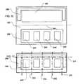
- FIG. 12is a top plan view of a component according to yet another embodiment of the invention.
- FIG. 13is an elevational view of the package made using the component of FIG. 12.
- FIG. 14is a plan view of the components depicted in FIG. 13.
- FIGS. 15 and 16are elevational views showing the package of FIGS. 13 and 14 in conjunction with other components.
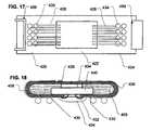
- FIG. 17is a plan view of a component according to yet another embodiment of the invention.
- FIG. 18is an elevational view of the component of FIG. 15 at a later stage of manufacture.
- a component according to one embodiment of the inventionincludes a dielectric substrate 20 in the form of an elongated strip having a first part 22 adjacent one end and a second part 24 adjacent the opposite end.
- the substratehas an interior surface 26 (the surface facing upwardly in FIG. 1) and an exterior surface 28 (facing downwardly in FIG. 1).
- a set of electrically conductive mounting terminals 30(FIG. 2) are provided on the first part 22 of the substrate. Terminals 30 are disposed at or near the interior surface 26 of the substrate and exposed to the exterior surface through holes or vias 32 extending through the substrate.
- Connecting terminals 34(FIG. 3) are provided in the second part 24 of the substrate. The connecting terminals are exposed to the external surface 28 of the substrate through holes 36 .
- the substratealso includes electrically conductive traces 38 extending between the first and second parts of the substrate and interconnecting at least some of the connecting terminals 34 with at least some of the mounting terminals 30 . Only a few of the traces 38 are depicted in FIG. 1 for clarity of illustration.
- Substrate 20may be formed from essentially any flexible dielectric material as, for example, one or more layers of a dielectric such as polyimide, BT or flexibilized epoxy.
- the conductive features such as terminals 32 and 34 and traces 38may be formed from a conventional metallic elements of the type commonly used in flexible circuitry as, for example, copper or gold formed by selective deposition such as plating or by selective removal from a layer, as by etching.
- the techniques commonly employed to make flexible circuitrycan be employed in fabrication of substrate 20 and the metallic features thereon.
- the substratemay include additional features as, for example, one or more additional layers of traces and electrically conductive planes such as metallic layers which can serve as a ground or power planes and which cooperate with the traces to form controlled impedance striplines.
- a first microelectronic device 40such as a semiconductor chip (FIG. 2) is mounted on the interior surface 26 of the substrate in the first area 22 .
- Device 40is electrically connected to at least some of the conductive features on the substrate in a conventional manner as, for example, by wire bonding using fine wires 42 to connect contacts on the chip to metallic elements of the substrate such as terminals 30 or traces 38 .
- the substrate 20is engaged in a mold 44 (FIG. 4).
- the moldmay be a conventional transfer, injection, compression mold having a first part 46 and a second part 48 .
- the first mold part 46has a parting surface 49 , which engages the interior surface 26 of the substrate.
- the second mold part 48engages the exterior surface.
- a first element cavity 50 and a second element cavity 52are provided in the first mold part 46 . These cavities are open to the parting surface 49 of the first mold part.
- Cavity 50is in the form of a generally rectangular block or mass 54 (FIG.
- mold part 46may be provided with one or more elements 68 arranged to move in the directions parallel to the parting plane 49 of the mold (to the left or right in FIG. 4) when the mold opens.
- elementsare commonly referred to in the mold making art as “side draws.” Numerous techniques for moving side draws in conjunction with the opening and closing motion of the mold are well known to those skilled in the mold making art.
- Cavity 52is in the form of a generally rectilinear U or three-sided box having a base wall 60 and a pair of side walls 62 projecting from the base wall. Only that part of cavity 52 which forms the base wall 60 (FIG. 1) is visible in the sectional view of FIG. 4. Also, as best seen in FIGS. 1 and 3, the interior surfaces of side walls 62 of the element 58 formed in the second element cavity 50 (FIG. 4) are provided with undercuts 70 and with lead-in chamfers 72 adjacent the top edges of these walls, remote from substrate 20 . Mold element 46 may include a core or internal element (not shown) arranged to form these features. The core may be collapsible or otherwise moveable so as to allow extraction of the molded part from this region of the mold.
- the mold making techniques used to permit molding of the desired shapeare well-known to those skilled in the mold making art.
- cavities 50 and 52are parts of a common mold 44 , these cavities may be formed in extremely precise spatial relationship to one another.
- Substrate 20is engaged in mold 44 in registration with cavities 50 and 52 , so that features of the substrate such as the edges of the dielectric layer and the terminals 34 and 30 (FIGS. 2 and 3) lie in pre-determined spatial relationships to the cavities.
- substrate 20may be provided with holes in pre-determined spatial relationship to other features of the substrate.
- Pins 76which only one is visible in FIG. 4, may extend from one or both of the mold parts 46 and 48 through the substrate.
- a moldable encapsulantsuch as a thermosetting or thermoplastic polymer composition is introduced into cavities 50 and 52 through channels 78 in the mold, until the encapsulant fills the cavities.
- the encapsulantis then brought to a solid condition by chemical reaction or by cooling.
- the material in its solid conditionis relatively rigid.
- thermal setting resinssuch as epoxies and phenolics may be employed.
- suitable resinsinclude those sold under the designations EME-7730 and EME-7730L by the Sumitomo Bakelite Company Limited of Tokyo, Japan.
- the partAfter the encapsulating material has been introduced into cavities 50 and 52 and brought to a solid condition, the part is ejected from the mold using conventional techniques.
- the componenthas a first alignment element in the form of mass 54 (FIGS. 1 and 2) covering the first microelectronic device or chip 40 , the first element 54 being disposed on the first part 22 of substrate 20 .
- the componentalso has a U-shaped second alignment element 58 on the second part 24 of the substrate.
- Both of these alignment elementsoverlie the interior surface 26 of the substrate.
- a thin layer of an adhesive 80is applied on the interior surface 26 of the second part 24 of the substrate, within the region encompassed by the U-shaped second alignment element 58 .
- This layer of adhesivemay be provided as a pre-formed film of the type commonly referred to as a “dry pad” adhesive.
- substrate 20is a part of a larger sheet or tape.
- substrate 20can be formed as part of a continuous or semi-continuous tape which is advanced through the mold in a step-wise fashion, so as to form one or more sets of alignment elements on individual portions of the tape, so as to produce a large number of components in sequence.
- substrate 20is folded over upon itself by bending generally around an axis 82 (FIG. 1) between the first and second parts 22 and 24 of the substrate, so as to bring the substrate to the folded condition depicted in FIGS. 5 and 6.
- the second part 24 of the substrateoverlies the first part, with the interior surface 26 in the second part confronting the interior surface in the first part.
- the first alignment element or mass 54enters into the opening defined by the second alignment element 58 , so that mass 54 is disposed between the side walls 62 of the second element.
- the dimensions of the mass 54 and the dimensions of the second element 58are arranged to provide a close fit between the first element or mass 54 and the second or U-shaped element 58 .
- the first alignment element or mass 54desirably also abuts the back wall 60 (FIGS. 1 and 5) of the second alignment element 58 .
- the engaged first element 54 and second element 58hold the second part of substrate 20 in precise position relative to the first part 22 .
- the engaged elementslimit relative movement of the two parts 22 and 24 in at least some directions parallel to the planes of these parts. These directions, to the left and right in FIG. 6 and into and out of the plane of the drawing in FIG. 6, are referred to herein as “horizontal directions.”
- the engagement of the first and second alignment elements 54 and 58brings the two parts 22 and 24 of the substrate to the desired relative positions in the horizontal directions.
- connection terminals 34 on the second part 24at the top of the assembly, will lie in the desired positions in the horizontal directions relative to the mounting terminals 30 on the first part 22 of the substrate. Consequently, if a further element is mounted on connecting terminals 34 , that further element also can be precisely registered with the mounting terminals 30 in the horizontal directions.
- first element 54moves into engagement with second element 58 , the lead-in chamfers 72 on the walls of the second element and corresponding chamfers on the top of the first element aid in bringing the parts to the proper alignment.
- the ledge 56 on the mass or first elemententers into the undercuts 70 on the inside of the walls of the second element and, thus, locks the two elements together. This holds substrate 20 in the folded condition. Additionally, the adhesive layer 80 on the substrate interior surface bonds to the top of mass 54 , thereby further securing the elements in position.
- both of the alignment elementsare formed from a relatively rigid encapsulating material
- the second element 58desirably has at least enough flexibility to permit ledge 56 to pass by the projecting portions of the walls and enter into undercut 70 .
- Walls 62 and 60are relatively thin and reside on the flexible substrate 20 . Thus, these elements are free to flex to the required degree to allow the wall 62 to splay outwardly slightly as the protruding ledge 56 of the first element enters between them and passes inwardly to the undercut.
- first and second alignment elements 54 and 58are formed in a common mold, they can be in precise registration with one another and can be precisely registered with the features of the substrate. Moreover, because these elements are formed from the same material at the same time and under the same molding conditions, factors such as dimensional changes in the molding material upon curing and dimensional changes in substrate 20 tend to affect both of these elements to substantially the same degree. All of these features help to contribute to the precise registration achievable in the folded article.
- the alignment elementsare provided at essentially zero additional cost.
- the first element 54is a mass of encapsulation material which would be required in any event to cover the first microelectronic device 40 .
- the incremental cost of forming the second element 58is infinitesimal; it consists principally of the cost of the molding material in this element. No additional molding time is required. Also, no additional operations are required to engage the alignment elements 54 and 58 with one another; they automatically engage one another when the substrate is folded.
- the package of FIGS. 5 and 6may be mounted to a circuit panel by attaching mounting terminals 30 (FIG. 6) to contact pads of a circuit panel (not shown). Before or after the package is mounted to the circuit panel, one or more additional devices 61 such as additional packaged or unpackaged microelectronic devices can be mounted to the top or second part 24 of the substrate, as by connecting such additional devices to the connection terminals 34 .
- the additional packagemay be a package identical to the package of FIGS. 5 and 6, two or more such packages can be connected in a stack.
- a component according to a further embodiment of the inventionis similar to the component discussed above, in that it incorporates a substrate 120 having a first part 122 and a second part 124 .
- a first microelectronic device or semiconductor element 140(FIG. 8) is mounted to the first part 122 of the substrate and a first alignment element 154 is formed as a mass of an encapsulant covering the first microelectronic device.
- the component of FIGS. 7 and 8also has a second microelectronic device 141 such as a second semiconductor chip (FIG. 8) mounted to the second part 124 of the substrate.
- the second alignment element 158is in the form of a second mass of encapsulant covering the second microelectronic device 141 .
- This second element or masshas an opening or recess 159 in its top surface sized to receive mass 154 .
- the first element 154is engaged in recess 159 of the second element 158 .
- the engaged alignment elementsconstrain the first and second parts 120 and 124 of the substrate and guide these parts into the proper alignment during the folding operation.
- a component according to this embodiment of the inventionmay be formed by a process similar to that discussed above.
- a first chip or microelectronic device 140is received in one cavity of the mold; whereas the second chip or microelectronic device 141 is received in another cavity in the same mold, so that once again the two alignment elements are formed in the same molding operation.
- the component and folded package of FIG. 9may have the other features discussed above with reference to FIGS. 1 - 6 , such as mounting terminals on one part of the substrate for mounting the folded package to a circuit panel and connecting terminals on the opposite part of the substrate for connecting additional elements or for testing the finished product. Here again, these two sets of terminals will be held in precise registration with one another.
- the mating alignment elements of FIGS. 7 - 9do not include undercuts to hold the assembly in the folded condition.
- An adhesive(not shown) may be provided on one or both of the alignment elements for this purpose.
- the component of FIG. 10includes several microelectronic devices 240 , all enclosed in a common mass or overmolding 254 , which serves as a first alignment element during the folding operation discussed below.
- the componentalso has a large second alignment element 258 on the same large, unitary substrate 220 .
- Elements 254 and 258can be formed by a molding process similar to that discussed above. In the molding process, all of the microelectronic devices 240 are encapsulated simultaneously. After the alignment elements 254 and 258 have been formed, the substrate is folded generally about axis 282 so as to bring the component to the folded condition depicted in FIG. 11, with alignment elements 254 and 258 inter-engaged with one another.
- the engaged alignment elementsassure that the overlapping portions of the substrate are in precise registration with one another.
- an adhesivesuch as an adhesive layer 280 carried by the substrate is used to form a bond which secures the substrate in its folded condition.
- the alignment elementsneed not have locking features such as the ridge and undercuts discussed above.
- Other types of adhesivemay be employed as, for example, an adhesive carried on the top surface of element 254 or a flowable adhesive applied to the assembly during or after folding.
- the componentmay be severed, as by cutting along lines 202 so as to separate portions of the folded component from one another and form individual units, each including one or more of the microelectronic devices 240 and the associated portions of the folded substrate.
- the substratecan be severed along further lines 204 so as to trim off portions of the substrate occupied by the second alignment element 258 , which is no longer needed after the adhesive bond has been formed.
- Assembliessuch as that discussed above with reference to FIGS. 7 - 9 , where microelectronic devices are present on both parts of the substrate, may also include multiple devices. In such an arrangement, each of the masses or alignment elements 154 and 158 may be a relatively large mass including numerous microelectronic devices. These masses are severed along with the substrate when the individual units are separated from one another.
- the component depicted in FIG. 12has a first alignment element 354 formed from an encapsulation material covering a first semiconductor device or chip 340 disposed in a first or central part 322 of the substrate.
- the componentalso has a second alignment element 358 disposed in a second or proximal end part 324 of the substrate extending outwardly from the first part 322 in a first or proximal direction.
- the component in accordance with this embodimentadditionally has a third alignment element 359 disposed in a third or distal end part 325 of the substrate extending away from the first pr central part in the opposite, distal direction (to the left as seen in the unfolded plan view of FIG. 12).
- FIG. 12In the folded condition (FIG.
- the proximal and distal end parts 324 and 325both overlap the central part 322 and the first alignment element or device encapsulation 354 .
- Both the second alignment element 358 and the third alignment element 359are engaged with the first alignment element 354 during the folding operation.
- the alignment elementsthus guide both of the proximal and distal end parts 324 and 325 into a precise, pre-determined registration with the first part 322 and also into a precise, pre-determined positional relationship with one another. This assures that connection terminals 334 on the second or proximal end part 324 and connection terminals 335 on the third or distal end part 325 will lie in pre-determined positions relative to one another. For example, the distance D (FIG.
- terminals 334 and 335 on the proximal and distal end parts of the substrateform a unified array which can be used, for example, to make connections with an additional device such as a further semiconductor chip 327 (FIG. 15).
- the mounting terminals 330can be bonded to corresponding circuit pads 302 on a circuit board 304 or other circuit panel.
- the terminals 330 on the first part 322 of the substrateare exposed at the bottom of the folded structure. If the array formed by connection terminals 334 and 335 matches the array of mounting terminals 330 , the package in the folded condition can be stacked with other identical packages as seen in FIG. 16. In this embodiment as well, the mounting terminals 330 on the bottom of the lower-most unit in the stack can be bonded to pads 302 of a circuit panel.
- the component discussed above with reference to FIG. 12has a proximal set of traces 306 extending along the substrate from the first or central part 322 of the substrate to the second or proximal part 324 and has another set of traces 308 extending from the first or central part 322 to the third or distal part 325 .
- connection terminals 334 in the second or proximal part 324 of the substrateare connected to at least some of the mounting terminals 330 in the first or central part 322 of the substrate or to the microelectronic device or chip 340 on the first part of the substrate by the traces of the first set, whereas at least some of the connection terminals 335 on the third or distal part of the substrate are connected to the mounting terminals or first microelectronic device in the first or central part 322 by the distal set of traces 308 .
- the combined array of terminals 334 and 335 at the top of the packageis connected to terminals 330 and device 340 at the bottom of the package in part by the proximal set of traces 306 extending across one fold on one side of the folded structure and in part by the distal set of traces 308 extending across another fold on the other side of the structure.
- This arrangementsignificantly simplifies routing of the traces within the substrate.
- the number of traces in each setcan be one-half the number which would be required to connect all of the terminals 334 and 335 using a single set of traces extending across a single fold.
- This simplified routingcan reduce the number of metallic layers required in the substrate. In many cases, all of the traces can be formed in a single layer.
- the component of FIG. 17also includes a substrate in the form of an elongated strip having a first or central part 422 , a second or proximal end part 424 extending on one side of first or central part and a third or distal end part 425 extending on the opposite side of the central part 422 .
- terminals 434 and 435are connected to the device, to terminals 430 in the first or central part 422 of the substrate, or both, by separate sets of traces 406 and 408 extending in opposite directions from the first or central part of the substrate to the proximal and distal parts of the substrate and, hence, extending around opposite folds in the folded configuration (FIG. 18).
- first alignment element 458at one end, on second or proximal part 424 of the substrate, and has a second alignment element 459 at the opposite end, in the third or distal part 425 of the substrate.
- These alignment elementsare arranged to engage one another in the folded condition of the substrate so as to maintain the second or proximal part 424 of the substrate in a pre-determined positional relationship to the third or distal part 425 , and thereby maintain terminals 434 in a pre-determined positional relationship to terminals 435 .
- the chip or first microelectronic device 440is not covered by an encapsulant at the time of folding and does not serve as an alignment element. Also, as best seen in FIG.
- the traces 406 and 408are disposed on the exterior surface of the substrate and the chip 440 is connected to these terminals by conductive elements such as wire bonds 402 extending through a hole in the substrate.
- conductive elementssuch as wire bonds 402 extending through a hole in the substrate.
- Other forms of conductorsmay be used as, for example, leads formed integrally with the traces or with the terminals 430 on the first part of the substrate.
- An encapsulant 404may be provided to cover these leads.
- a further encapsulant 406may be provided within the folded substrate so that the further encapsulant provides an additional adhesive bond between the overlapping portions of the substrate. This additional adhesive bond secures the various parts of the substrate in position relative to one another.
- connection terminalscan be mounted to the circuit board by connection terminals 34 and additional microelectronic devices or packages can be connected to mounting terminals 30 .
- the combined array of connection terminals 334 and 335 in the embodiment of FIGS. 13 - 16can be used to mount the package to the circuit panel, so that the mounting terminals 330 face upwardly, away from the circuit panel.
- the mounting terminalscan be used to connect an additional package or other device.
- terminals other than the solder-bondable pads shown in the drawings, such as pins projecting from the substrate and adapted to be received in a socketcan be employed.
- the inter-engagement of alignment elementscan be used in more complex folded structures.
- a substrate in a generally cruciform shape having multiple arms extending from a central regioncan be folded so that the various arms all overlie the central region, and so that microelectronic devices positioned on all of the arms are stacked one above the other.
- Such a structurecan be provided with alignment elements on two or more parts of the substrate as, for example, on one or more of the various arms, on the central portion, or both, so as to hold the parts of the substrate in a desired positional relationship when the substrate is in a folded condition.
- alignment elementshaving other shapes can be employed.
- an alignment element on one part of a substratemay define a circular or cylindrical recess, or a plurality of such recesses, whereas an alignment element on the mating part of the substrate may define one or more pins adapted to fit within such recess or recesses.
- the alignment elementscan be features of the substrate itself. Features of the substrate itself which constitute alignment elements should be considered as “attached” or “mounted” to the substrate. Also, the alignment elements can be formed from essentially any material.
- a pin-shaped metallic alignment elementcan be formed by processes similar to those used to form terminals and via liners, whereas a recess can be formed by processes used to form vias in the substrate.
- the alignment elementscan be formed at essentially no additional cost.
- the substratemay be formed with holes used for aligning and registering the substrate during processing operation, such as the sprocket holes commonly provided on tape-like substrates. An alignment element projecting from a part of the substrate remote from one set of socket holes may engage that set of socket holes when the substrate is folded.
Landscapes
- Engineering & Computer Science (AREA)
- Microelectronics & Electronic Packaging (AREA)
- Power Engineering (AREA)
- Physics & Mathematics (AREA)
- Condensed Matter Physics & Semiconductors (AREA)
- General Physics & Mathematics (AREA)
- Computer Hardware Design (AREA)
- Encapsulation Of And Coatings For Semiconductor Or Solid State Devices (AREA)
Abstract
Description
- The present application claims benefit of U.S. Provisional Patent Application Serial No. 60/403,939, filed Aug. 16, 2002, the disclosure of which is hereby incorporated by reference herein.[0001]
- The present invention relates to microelectronic assemblies and to components and methods for making the same.[0002]
- Certain microelectronic packages are made using a sheet like element incorporating a dielectric layer structure and mounting terminals disposed on this structure. Some or all of the terminals are connected to the microelectronic device to be packaged. In many cases, the active microelectronic device such as a semiconductor chip is covered by an encapsulant. The encapsulant commonly is molded in place on the dielectric layer so that the mass of encapsulant has a preselected shape, and so that the encapsulant covers the microelectronic device. The encapsulant may also cover features such as wire bonds which connect the actual chip to the terminals. Such a package may be mounted on a circuit panel such as a circuit board by bonding or otherwise connecting the mounting terminals to contact pads on the circuit board.[0003]
- Various proposals have been advanced for stacking plural chips one above the other in a common package. One such arrangement includes a substrate having a dielectric structure substantially larger in area than the area of a single microelectronic device or chip. Several microelectronic devices are mounted to the substrate in different parts of the substrate and the substrate is folded so that the various microelectronic devices are stacked one above the other and so that the mounting terminals on the substrate are disposed at the bottom of the stack. Typically, the substrate has electrically conductive traces extending along the dielectric structure. These traces interconnect the microelectronic devices with one another, with the mounting materials or both in the completed structure. In one such structure, the substrate is in the form of an elongated strip and the various microelectronic devices are attached at spaced apart locations along the length of the strip. The strip is then folded into a serpentine configuration so that the microelectronic devices are stacked one above the other.[0004]
- If the substrate is folded in precisely the right configuration, the various microelectronic devices will be disposed in the correct locations, one above the other. The entire package can be placed in an area of the circuit board only slightly larger than the area occupied by a single microelectronic device. However, inaccuracies in folding the substrate can cause parts of the package to lie in positions different from its nominal position relative to the mounting terminals. This effectively increases the overall size of the package. Neighboring components mounted to the circuit board must be located at a larger distance from the stack so as to provide clearance sufficient to accommodate this internal misalignment within the stack. Moreover, the piece-to-piece differences between nominally identical packages caused by folding inaccuracies can complicate the task of handling and feeding the stacked packages during automated assembly operations as, for example, during mounting to the circuit panel.[0005]
- As disclosed in commonly assigned U.S. Pat. No. 6,225,688, the disclosure of which is hereby incorporated by reference herein, a folding operation may be performed using a substrate having a plurality of microelectronic devices, or only a single microelectronic device, and also having additional terminals referred to herein as connection terminals. After folding, the mounting terminals of the substrate lie on the bottom of the folded structure, whereas the connection terminals lie on the top of the folded structure. Additional elements such as additional microelectronic packages can be mounted on top of the folded structure and connected to the folded structure through the connection terminals. Also, the connection terminals can be used as test terminals for testing the folded structure before or after mounting the same to a circuit panel. Inaccuracies in folding the substrate place the connection terminals at a position other than their nominal position. If an additional microelectronic element is mounted on top of the folded structure using the connection terminals, the additional microelectronic element will be displaced from its nominal position further, thus increasing the overall size of the package in the manner discussed above. Also, displacement of the connecting terminals from their nominal position can complicate the tasks of connection an additional element to the connection terminals and the task of engaging the connecting terminals with a test fixture during a testing operation.[0006]
- It would be desirable to provide further improvement in substrate folding processes.[0007]
- One aspect of the present invention provides a method of making a microelectronic package. A method according to this aspect of the present invention includes the step of providing first and second alignment elements on first and second parts of a substrate bearing a first microelectronic device and then folding the substrate so that the first and second alignment elements engage one another. Most preferably, the engaged first and second elements hold the second part of the substrate in a preselected disposition relative to the first part of the substrate. For example, the folding step may be performed so that the first and second parts of the substrate extend in planes substantially parallel to one another after the folding step and so that the engaged first and second elements limit the movement of the second part relative to the first part in at least some directions parallel to the planes of these parts. For example, the folding step may be performed so that the first and second parts of the substrate overlap one another and lie in substantially parallel planes, with the first microelectronic device disposed between the first and second parts of the substrate.[0008]
- The first alignment element may be a mass of encapsulant at least partially covering the first microelectronic device. Where a second microelectronic device is provided on the substrate prior to folding, the second alignment element also may be a mass of encapsulant at least partially covering the second microelectronic device. Alternatively, one or both of the alignment elements may be a part separate from a microelectronic device. In one configuration, the first alignment element is a mass of encapsulant covering a first semiconductor chip, whereas the second alignment element generally in the form of a rectilinear ring or U-shaped element which engages the mass when the substrate is folded.[0009]
- Most preferably, both of the alignment elements are formed using a common tool as, for example, by molding both alignment elements in place on the substrate using the same mold. This molding operation may be the same molding operation used to apply the encapsulant on the first microelectronic device. Thus, the alignment elements can be provided at essentially no additional cost. Alignment elements which are separate from the microelectronic device occupy only a minimal additional area on the substrate.[0010]
- The method may include the additional step of forming an adhesive bond during or after the folding steps but the adhesive bond locks the second part of the substrate in position relative to the first part of the substrate set by the engagement between the alignment elements. For example, a part of the substrate may bear an adhesive layer and this layer may form a bond to the encapsulant mass covering the first microelectronic device. Where such an adhesive bond is formed, the alignment elements can be removed after the folding step as, for example, by cutting away that portion of the substrate bearing one of the alignment elements. The method may be applied to a substrate bearing a plurality of microelectronic devices as, for example, a plurality of microelectronic devices. After folding and, preferably, after formation of an adhesive bond, the substrate may be severed so as to form individual units each including a portion of the folded substrate and one or more of the microelectronic devices.[0011]
- A further aspect of the present invention provides an intermediate structure for making a microelectronic package. The structure according to this aspect of the invention desirably includes a substrate having first and second parts and a first microelectronic device attached to the substrate in one of the parts. A first alignment element is attached to the first part of the substrate and the second alignment element is attached to the second part of the substrate. The substrate is adapted for folding so as to bring the first and second alignment elements into engagement with one another. The alignment elements are adapted to engage one another so as to retain the second part of the substrate in a preselected disposition relative to the first part of the substrate. Here again, one or both of the alignment elements may include a mass of encapsulant at least partially covering a microelectronic device. The substrate may be a partially or completely flexible sheet like element.[0012]
- Yet another aspect of the invention provides a microelectronic package including a substrate having first and second parts. The package according to this aspect of the invention desirably also includes a first alignment element attached to the first part of the substrate and a second alignment element attached to the second part of the substrate. The substrate is folded so that the alignment elements are engaged with one another and retain the second part of the substrate in a preselected disposition relative to the first part of the substrate. As discussed above in connection with the method, the substrate desirably is folded so that the first and second parts of the substrate lie at least partially in planes parallel to one another and so that the engaged first and second elements limit movement of the second part of the substrate relative to the first part in at least some directions parallel to the planes.[0013]
- A further aspect of the present invention provides a microelectronic package comprising an elongated substrate such as an elongated strip having a proximal part, a distal part and a central part disposed between the proximal and distal parts. The package includes a microelectronic device mounted to one of these parts. The substrate is folded so that the proximal and distal parts overlie the central part, and so that the microelectronic device disposed between the central part and at least one of the proximal and distal parts. For example, the microelectronic device may be mounted on the central part and both the proximal and distal parts may overlie the microelectronic device. The substrate has a proximal set of traces extending along the substrate from the central part to the proximal part and has a distal set of traces extending along the substrate from the central part to the distal part. Thus, in the folded condition, the traces extend across folds on opposite sides of the structure. The substrate desirably has a set of central terminals disposed on the central part, a set of proximal terminals disposed on the proximal part and a set of distal terminals disposed on the distal part. In the folded condition, the proximal and distal terminals desirably form an array of terminals on one side of the package. The proximal set of traces connects at least some of said proximal terminals with at least some of the central terminals, with the microelectronic device, or both, whereas the distal set of traces connects the distal terminals with at least some of said central terminals, with the microelectronic device, or both. The use of two sets of traces extending across two separate folds to connect the array of terminals with the remainder of the package greatly simplifies routing of the traces. This can reduce the number of metallic layers required in the substrate. Most preferably, the substrate includes only a single layer of traces.[0014]
- FIG. 1 is a diagrammatic perspective view of an in process article according to one embodiment of the invention.[0015]
- FIG. 2 is a diagrammatic sectional view taken along the line[0016]2-2 in FIG. 1.
- FIG. 3 is a diagrammatic sectional view taken along line[0017]3-3 in FIG. 1.
- FIG. 4 is a diagrammatic sectional view of a mold used in forming the article of FIGS.[0018]1-3 during one stage in production of the article.
- FIG. 5 is a diagrammatic perspective view of a package formed from the article of FIGS.[0019]1-3.
- FIG. 6 is a diagrammatic sectional view taken along line[0020]6-6 in FIG. 5.
- FIG. 7 is a diagrammatic plan view of an in process article in accordance with a further embodiment of the invention.[0021]
- FIG. 8 is a diagrammatic sectional view taken along line[0022]8-8 in FIG. 7.
- FIG. 9 is a sectional view similar to FIG. 8 but depicting the finished package formed from the components of FIGS. 7 and 8.[0023]
- FIG. 10 is a diagrammatic plan view of an in process component according to a further embodiment of the invention.[0024]
- FIG. 11 is a diagrammatic plan view of the component of FIG. 10 at a later stage of manufacture.[0025]
- FIG. 12 is a top plan view of a component according to yet another embodiment of the invention.[0026]
- FIG. 13 is an elevational view of the package made using the component of FIG. 12.[0027]
- FIG. 14 is a plan view of the components depicted in FIG. 13.[0028]
- FIGS. 15 and 16 are elevational views showing the package of FIGS. 13 and 14 in conjunction with other components.[0029]
- FIG. 17 is a plan view of a component according to yet another embodiment of the invention.[0030]
- FIG. 18 is an elevational view of the component of FIG. 15 at a later stage of manufacture.[0031]
- A component according to one embodiment of the invention includes a[0032]
dielectric substrate 20 in the form of an elongated strip having afirst part 22 adjacent one end and asecond part 24 adjacent the opposite end. The substrate has an interior surface26 (the surface facing upwardly in FIG. 1) and an exterior surface28 (facing downwardly in FIG. 1). A set of electrically conductive mounting terminals30 (FIG. 2) are provided on thefirst part 22 of the substrate.Terminals 30 are disposed at or near theinterior surface 26 of the substrate and exposed to the exterior surface through holes orvias 32 extending through the substrate. Connecting terminals34 (FIG. 3) are provided in thesecond part 24 of the substrate. The connecting terminals are exposed to theexternal surface 28 of the substrate through holes36. The substrate also includes electricallyconductive traces 38 extending between the first and second parts of the substrate and interconnecting at least some of the connectingterminals 34 with at least some of the mountingterminals 30. Only a few of thetraces 38 are depicted in FIG. 1 for clarity of illustration.Substrate 20 may be formed from essentially any flexible dielectric material as, for example, one or more layers of a dielectric such as polyimide, BT or flexibilized epoxy. The conductive features such asterminals substrate 20 and the metallic features thereon. The substrate may include additional features as, for example, one or more additional layers of traces and electrically conductive planes such as metallic layers which can serve as a ground or power planes and which cooperate with the traces to form controlled impedance striplines. - A first[0033]
microelectronic device 40 such as a semiconductor chip (FIG. 2) is mounted on theinterior surface 26 of the substrate in thefirst area 22.Device 40 is electrically connected to at least some of the conductive features on the substrate in a conventional manner as, for example, by wire bonding usingfine wires 42 to connect contacts on the chip to metallic elements of the substrate such asterminals 30 or traces38. - In a manufacturing process used to form the component of FIGS.[0034]1-3, the
substrate 20, with first microelectronic device orchip 40 thereon, is engaged in a mold44 (FIG. 4). The mold may be a conventional transfer, injection, compression mold having afirst part 46 and asecond part 48. Thefirst mold part 46 has aparting surface 49, which engages theinterior surface 26 of the substrate. Thesecond mold part 48 engages the exterior surface. Afirst element cavity 50 and asecond element cavity 52 are provided in thefirst mold part 46. These cavities are open to theparting surface 49 of the first mold part.Cavity 50 is in the form of a generally rectangular block or mass54 (FIG. 1) having a projectingridge 56 at the top of the mass, remote fromsubstrate 20. As best seen in FIG. 4, the chip or firstmicroelectronic device 40 is disposed within thefirst element cavity 50 when the substrate is engaged with the mold. Theportion 66 of cavity50 (FIG. 4) which forms ridge56 (FIG. 1) extends outwardly from the remainder ofcavity 50 in a direction perpendicular to the direction of motion of the molded part during ejection from the mold and forms a “undercut” in the mold. To permit extraction of the molded article from the mold,mold part 46 may be provided with one ormore elements 68 arranged to move in the directions parallel to theparting plane 49 of the mold (to the left or right in FIG. 4) when the mold opens. Such elements are commonly referred to in the mold making art as “side draws.” Numerous techniques for moving side draws in conjunction with the opening and closing motion of the mold are well known to those skilled in the mold making art. - [0035]
Cavity 52 is in the form of a generally rectilinear U or three-sided box having abase wall 60 and a pair ofside walls 62 projecting from the base wall. Only that part ofcavity 52 which forms the base wall60 (FIG. 1) is visible in the sectional view of FIG. 4. Also, as best seen in FIGS. 1 and 3, the interior surfaces ofside walls 62 of theelement 58 formed in the second element cavity50 (FIG. 4) are provided withundercuts 70 and with lead-inchamfers 72 adjacent the top edges of these walls, remote fromsubstrate 20.Mold element 46 may include a core or internal element (not shown) arranged to form these features. The core may be collapsible or otherwise moveable so as to allow extraction of the molded part from this region of the mold. Here again, the mold making techniques used to permit molding of the desired shape are well-known to those skilled in the mold making art. - Because[0036]
cavities common mold 44, these cavities may be formed in extremely precise spatial relationship to one another.Substrate 20 is engaged inmold 44 in registration withcavities terminals 34 and30 (FIGS. 2 and 3) lie in pre-determined spatial relationships to the cavities. Merely by way of example,substrate 20 may be provided with holes in pre-determined spatial relationship to other features of the substrate.Pins 76, which only one is visible in FIG. 4, may extend from one or both of themold parts - With[0037]
substrate 20 disposed in the mold, a moldable encapsulant such as a thermosetting or thermoplastic polymer composition is introduced intocavities channels 78 in the mold, until the encapsulant fills the cavities. The encapsulant is then brought to a solid condition by chemical reaction or by cooling. Preferably, the material in its solid condition is relatively rigid. Essentially any material commonly usable as a protective overmolding material in electronic packaging can be employed. Merely by way of example, thermal setting resins such as epoxies and phenolics may be employed. Some suitable resins include those sold under the designations EME-7730 and EME-7730L by the Sumitomo Bakelite Company Limited of Tokyo, Japan. These resins have a flexural modulus of about 2400 kg/mm2at 25° C. and about 150-155 kg/mm2at 240° C. Resins of this type adhere well to electronic components and to dielectric polymers such as polyimide. After the encapsulating material has been introduced intocavities chip 40, thefirst element 54 being disposed on thefirst part 22 ofsubstrate 20. The component also has a U-shapedsecond alignment element 58 on thesecond part 24 of the substrate. Both of these alignment elements overlie theinterior surface 26 of the substrate. A thin layer of an adhesive80 is applied on theinterior surface 26 of thesecond part 24 of the substrate, within the region encompassed by the U-shapedsecond alignment element 58. This layer of adhesive may be provided as a pre-formed film of the type commonly referred to as a “dry pad” adhesive. - Although the processing steps used to form the component of FIGS.[0038]1-3 have been described with reference to a single component, it should be appreciated that these processing steps can be performed while
substrate 20 is a part of a larger sheet or tape. For example,substrate 20 can be formed as part of a continuous or semi-continuous tape which is advanced through the mold in a step-wise fashion, so as to form one or more sets of alignment elements on individual portions of the tape, so as to produce a large number of components in sequence. - In the next stage of the process,[0039]
substrate 20 is folded over upon itself by bending generally around an axis82 (FIG. 1) between the first andsecond parts second part 24 of the substrate overlies the first part, with theinterior surface 26 in the second part confronting the interior surface in the first part. The first alignment element ormass 54 enters into the opening defined by thesecond alignment element 58, so thatmass 54 is disposed between theside walls 62 of the second element. The dimensions of themass 54 and the dimensions of thesecond element 58 are arranged to provide a close fit between the first element ormass 54 and the second orU-shaped element 58. The first alignment element ormass 54 desirably also abuts the back wall60 (FIGS. 1 and 5) of thesecond alignment element 58. The engagedfirst element 54 andsecond element 58 hold the second part ofsubstrate 20 in precise position relative to thefirst part 22. Stated another way, the engaged elements limit relative movement of the twoparts second alignment elements parts connection terminals 34 on thesecond part 24, at the top of the assembly, will lie in the desired positions in the horizontal directions relative to the mountingterminals 30 on thefirst part 22 of the substrate. Consequently, if a further element is mounted on connectingterminals 34, that further element also can be precisely registered with the mountingterminals 30 in the horizontal directions. - As[0040]
first element 54 moves into engagement withsecond element 58, the lead-inchamfers 72 on the walls of the second element and corresponding chamfers on the top of the first element aid in bringing the parts to the proper alignment. Theledge 56 on the mass or first element enters into theundercuts 70 on the inside of the walls of the second element and, thus, locks the two elements together. This holdssubstrate 20 in the folded condition. Additionally, theadhesive layer 80 on the substrate interior surface bonds to the top ofmass 54, thereby further securing the elements in position. Although both of the alignment elements are formed from a relatively rigid encapsulating material, thesecond element 58 desirably has at least enough flexibility to permitledge 56 to pass by the projecting portions of the walls and enter into undercut70.Walls flexible substrate 20. Thus, these elements are free to flex to the required degree to allow thewall 62 to splay outwardly slightly as the protrudingledge 56 of the first element enters between them and passes inwardly to the undercut. - Because the first and[0041]
second alignment elements substrate 20 tend to affect both of these elements to substantially the same degree. All of these features help to contribute to the precise registration achievable in the folded article. The alignment elements are provided at essentially zero additional cost. Thefirst element 54 is a mass of encapsulation material which would be required in any event to cover the firstmicroelectronic device 40. The incremental cost of forming thesecond element 58 is infinitesimal; it consists principally of the cost of the molding material in this element. No additional molding time is required. Also, no additional operations are required to engage thealignment elements - The package of FIGS. 5 and 6 may be mounted to a circuit panel by attaching mounting terminals[0042]30 (FIG. 6) to contact pads of a circuit panel (not shown). Before or after the package is mounted to the circuit panel, one or more
additional devices 61 such as additional packaged or unpackaged microelectronic devices can be mounted to the top orsecond part 24 of the substrate, as by connecting such additional devices to theconnection terminals 34. The additional package may be a package identical to the package of FIGS. 5 and 6, two or more such packages can be connected in a stack. - A component according to a further embodiment of the invention (FIGS. 7 and 8) is similar to the component discussed above, in that it incorporates a[0043]
substrate 120 having afirst part 122 and asecond part 124. Here again, a first microelectronic device or semiconductor element140 (FIG. 8) is mounted to thefirst part 122 of the substrate and afirst alignment element 154 is formed as a mass of an encapsulant covering the first microelectronic device. The component of FIGS. 7 and 8 also has a secondmicroelectronic device 141 such as a second semiconductor chip (FIG. 8) mounted to thesecond part 124 of the substrate. Thesecond alignment element 158 is in the form of a second mass of encapsulant covering the secondmicroelectronic device 141. This second element or mass has an opening orrecess 159 in its top surface sized to receivemass 154. In the folded condition (FIG. 9), thefirst element 154 is engaged inrecess 159 of thesecond element 158. Here again, the engaged alignment elements constrain the first andsecond parts microelectronic device 140 is received in one cavity of the mold; whereas the second chip ormicroelectronic device 141 is received in another cavity in the same mold, so that once again the two alignment elements are formed in the same molding operation. The component and folded package of FIG. 9 may have the other features discussed above with reference to FIGS.1-6, such as mounting terminals on one part of the substrate for mounting the folded package to a circuit panel and connecting terminals on the opposite part of the substrate for connecting additional elements or for testing the finished product. Here again, these two sets of terminals will be held in precise registration with one another. The mating alignment elements of FIGS.7-9 do not include undercuts to hold the assembly in the folded condition. An adhesive (not shown) may be provided on one or both of the alignment elements for this purpose. - The component of FIG. 10 includes several[0044]
microelectronic devices 240, all enclosed in a common mass orovermolding 254, which serves as a first alignment element during the folding operation discussed below. The component also has a largesecond alignment element 258 on the same large,unitary substrate 220.Elements microelectronic devices 240 are encapsulated simultaneously. After thealignment elements axis 282 so as to bring the component to the folded condition depicted in FIG. 11, withalignment elements adhesive layer 280 carried by the substrate is used to form a bond which secures the substrate in its folded condition. Thus, the alignment elements need not have locking features such as the ridge and undercuts discussed above. Other types of adhesive may be employed as, for example, an adhesive carried on the top surface ofelement 254 or a flowable adhesive applied to the assembly during or after folding. - After the adhesive has set and formed a bond, the component may be severed, as by cutting along[0045]
lines 202 so as to separate portions of the folded component from one another and form individual units, each including one or more of themicroelectronic devices 240 and the associated portions of the folded substrate. At the same time, the substrate can be severed alongfurther lines 204 so as to trim off portions of the substrate occupied by thesecond alignment element 258, which is no longer needed after the adhesive bond has been formed. Assemblies such as that discussed above with reference to FIGS.7-9, where microelectronic devices are present on both parts of the substrate, may also include multiple devices. In such an arrangement, each of the masses oralignment elements - The component depicted in FIG. 12 has a[0046]
first alignment element 354 formed from an encapsulation material covering a first semiconductor device orchip 340 disposed in a first orcentral part 322 of the substrate. The component also has asecond alignment element 358 disposed in a second orproximal end part 324 of the substrate extending outwardly from thefirst part 322 in a first or proximal direction. The component in accordance with this embodiment additionally has athird alignment element 359 disposed in a third ordistal end part 325 of the substrate extending away from the first pr central part in the opposite, distal direction (to the left as seen in the unfolded plan view of FIG. 12). In the folded condition (FIG. 13), the proximal anddistal end parts central part 322 and the first alignment element ordevice encapsulation 354. Both thesecond alignment element 358 and thethird alignment element 359 are engaged with thefirst alignment element 354 during the folding operation. The alignment elements thus guide both of the proximal anddistal end parts first part 322 and also into a precise, pre-determined positional relationship with one another. This assures thatconnection terminals 334 on the second orproximal end part 324 andconnection terminals 335 on the third ordistal end part 325 will lie in pre-determined positions relative to one another. For example, the distance D (FIG. 14) between a row ofterminals 334 on second orproximal end part 324 and the neighboring row ofterminals 335 on third ordistal end part 325 is precisely determined by the alignment elements so that this distance can be maintained within a reasonable tolerance during mass production of the packages. Thus, theterminals terminals 330 can be bonded tocorresponding circuit pads 302 on acircuit board 304 or other circuit panel. - In this embodiment as well, the[0047]
terminals 330 on thefirst part 322 of the substrate (FIG. 13) are exposed at the bottom of the folded structure. If the array formed byconnection terminals terminals 330, the package in the folded condition can be stacked with other identical packages as seen in FIG. 16. In this embodiment as well, the mountingterminals 330 on the bottom of the lower-most unit in the stack can be bonded topads 302 of a circuit panel. - The component discussed above with reference to FIG. 12 has a proximal set of[0048]
traces 306 extending along the substrate from the first orcentral part 322 of the substrate to the second orproximal part 324 and has another set oftraces 308 extending from the first orcentral part 322 to the third ordistal part 325. At least some of theconnection terminals 334 in the second orproximal part 324 of the substrate are connected to at least some of the mountingterminals 330 in the first orcentral part 322 of the substrate or to the microelectronic device orchip 340 on the first part of the substrate by the traces of the first set, whereas at least some of theconnection terminals 335 on the third or distal part of the substrate are connected to the mounting terminals or first microelectronic device in the first orcentral part 322 by the distal set oftraces 308. Thus, in the folded package, the combined array ofterminals terminals 330 anddevice 340 at the bottom of the package in part by the proximal set oftraces 306 extending across one fold on one side of the folded structure and in part by the distal set oftraces 308 extending across another fold on the other side of the structure. This arrangement significantly simplifies routing of the traces within the substrate. The number of traces in each set can be one-half the number which would be required to connect all of theterminals - The component of FIG. 17 also includes a substrate in the form of an elongated strip having a first or[0049]
central part 422, a second orproximal end part 424 extending on one side of first or central part and a third ordistal end part 425 extending on the opposite side of thecentral part 422. Here again,terminals terminals 430 in the first orcentral part 422 of the substrate, or both, by separate sets oftraces first alignment element 458 at one end, on second orproximal part 424 of the substrate, and has a second alignment element459 at the opposite end, in the third ordistal part 425 of the substrate. These alignment elements are arranged to engage one another in the folded condition of the substrate so as to maintain the second orproximal part 424 of the substrate in a pre-determined positional relationship to the third ordistal part 425, and thereby maintainterminals 434 in a pre-determined positional relationship toterminals 435. In the embodiment illustrated, the chip or firstmicroelectronic device 440 is not covered by an encapsulant at the time of folding and does not serve as an alignment element. Also, as best seen in FIG. 18, thetraces chip 440 is connected to these terminals by conductive elements such aswire bonds 402 extending through a hole in the substrate. Other forms of conductors may be used as, for example, leads formed integrally with the traces or with theterminals 430 on the first part of the substrate. Anencapsulant 404 may be provided to cover these leads. Afurther encapsulant 406 may be provided within the folded substrate so that the further encapsulant provides an additional adhesive bond between the overlapping portions of the substrate. This additional adhesive bond secures the various parts of the substrate in position relative to one another. - Numerous variations and combinations of the features discussed above can be utilized without departing from the present invention. In one such variant, the roles of the mounting terminals and connection terminals discussed above are reversed. For example, the package of FIGS. 5 and 6 can be mounted to the circuit board by[0050]
connection terminals 34 and additional microelectronic devices or packages can be connected to mountingterminals 30. Similarly, the combined array ofconnection terminals terminals 330 face upwardly, away from the circuit panel. The mounting terminals can be used to connect an additional package or other device. Also, terminals other than the solder-bondable pads shown in the drawings, such as pins projecting from the substrate and adapted to be received in a socket, can be employed. - The inter-engagement of alignment elements can be used in more complex folded structures. For example, as disclosed in commonly-assigned, co-pending U.S. patent application Ser. No. 10/077,388, filed Feb. 15, 2002, a substrate in a generally cruciform shape having multiple arms extending from a central region can be folded so that the various arms all overlie the central region, and so that microelectronic devices positioned on all of the arms are stacked one above the other. Such a structure can be provided with alignment elements on two or more parts of the substrate as, for example, on one or more of the various arms, on the central portion, or both, so as to hold the parts of the substrate in a desired positional relationship when the substrate is in a folded condition. Also, the particular shapes of the alignment elements discussed above are illustrative only. Alignment elements having other shapes can be employed. For example, an alignment element on one part of a substrate may define a circular or cylindrical recess, or a plurality of such recesses, whereas an alignment element on the mating part of the substrate may define one or more pins adapted to fit within such recess or recesses. In a further variant, the alignment elements can be features of the substrate itself. Features of the substrate itself which constitute alignment elements should be considered as “attached” or “mounted” to the substrate. Also, the alignment elements can be formed from essentially any material. Merely by way of example, a pin-shaped metallic alignment element can be formed by processes similar to those used to form terminals and via liners, whereas a recess can be formed by processes used to form vias in the substrate. Here again, the alignment elements can be formed at essentially no additional cost. In yet another arrangement, the substrate may be formed with holes used for aligning and registering the substrate during processing operation, such as the sprocket holes commonly provided on tape-like substrates. An alignment element projecting from a part of the substrate remote from one set of socket holes may engage that set of socket holes when the substrate is folded.[0051]
- As these and other variations and combinations of the features discussed above can be utilized without departing from the present invention, the foregoing description of the preferred embodiment should be taken by way of illustration rather than by way of limitation of the invention as defined by the claims.[0052]
Claims (29)
Priority Applications (1)
| Application Number | Priority Date | Filing Date | Title |
|---|---|---|---|
| US10/640,177US7053485B2 (en) | 2002-08-16 | 2003-08-13 | Microelectronic packages with self-aligning features |
Applications Claiming Priority (2)
| Application Number | Priority Date | Filing Date | Title |
|---|---|---|---|
| US40393902P | 2002-08-16 | 2002-08-16 | |
| US10/640,177US7053485B2 (en) | 2002-08-16 | 2003-08-13 | Microelectronic packages with self-aligning features |
Publications (2)
| Publication Number | Publication Date |
|---|---|
| US20040104470A1true US20040104470A1 (en) | 2004-06-03 |
| US7053485B2 US7053485B2 (en) | 2006-05-30 |
Family
ID=31888300
Family Applications (1)
| Application Number | Title | Priority Date | Filing Date |
|---|---|---|---|
| US10/640,177Expired - Fee RelatedUS7053485B2 (en) | 2002-08-16 | 2003-08-13 | Microelectronic packages with self-aligning features |
Country Status (3)
| Country | Link |
|---|---|
| US (1) | US7053485B2 (en) |
| AU (1) | AU2003265417A1 (en) |
| WO (1) | WO2004017399A1 (en) |
Cited By (36)
| Publication number | Priority date | Publication date | Assignee | Title |
|---|---|---|---|---|
| US20040229402A1 (en)* | 2001-10-26 | 2004-11-18 | Staktek Group, L.P. | Low profile chip scale stacking system and method |
| US20050062144A1 (en)* | 2001-10-26 | 2005-03-24 | Staktek Group, L.P. | Memory expansion and chip scale stacking system and method |
| US20050062141A1 (en)* | 2003-09-22 | 2005-03-24 | Salta Jose R. | Electronic package having a folded flexible substrate and method of manufacturing the same |
| US20050067688A1 (en)* | 2003-09-26 | 2005-03-31 | Tessera, Inc. | Structure and method of making capped chips including vertical interconnects having stud bumps engaged to surfaces of said caps |
| US20050116344A1 (en)* | 2003-10-29 | 2005-06-02 | Tessera, Inc. | Microelectronic element having trace formed after bond layer |
| US7033861B1 (en) | 2005-05-18 | 2006-04-25 | Staktek Group L.P. | Stacked module systems and method |
| US7053478B2 (en) | 2001-10-26 | 2006-05-30 | Staktek Group L.P. | Pitch change and chip scale stacking system |
| US7081373B2 (en) | 2001-12-14 | 2006-07-25 | Staktek Group, L.P. | CSP chip stack with flex circuit |
| US20060183270A1 (en)* | 2005-02-14 | 2006-08-17 | Tessera, Inc. | Tools and methods for forming conductive bumps on microelectronic elements |
| US20060278962A1 (en)* | 2005-06-09 | 2006-12-14 | Tessera, Inc. | Microelectronic loop packages |
| US7180167B2 (en) | 2001-10-26 | 2007-02-20 | Staktek Group L. P. | Low profile stacking system and method |
| US7202555B2 (en) | 2001-10-26 | 2007-04-10 | Staktek Group L.P. | Pitch change and chip scale stacking system and method |
| USRE39628E1 (en) | 1999-05-05 | 2007-05-15 | Stakick Group, L.P. | Stackable flex circuit IC package and method of making same |
| US20070138644A1 (en)* | 2005-12-15 | 2007-06-21 | Tessera, Inc. | Structure and method of making capped chip having discrete article assembled into vertical interconnect |
| US7265440B2 (en) | 2003-06-16 | 2007-09-04 | Tessera Technologies Hungary Kft. | Methods and apparatus for packaging integrated circuit devices |
| US7310458B2 (en) | 2001-10-26 | 2007-12-18 | Staktek Group L.P. | Stacked module systems and methods |
| US7309914B2 (en) | 2005-01-20 | 2007-12-18 | Staktek Group L.P. | Inverted CSP stacking system and method |
| US7335975B2 (en) | 2001-10-26 | 2008-02-26 | Staktek Group L.P. | Integrated circuit stacking system and method |
| US7371609B2 (en) | 2001-10-26 | 2008-05-13 | Staktek Group L.P. | Stacked module systems and methods |
| US20080157330A1 (en)* | 2006-12-28 | 2008-07-03 | Steffen Kroehnert | Semiconductor Device with Chip Mounted on a Substrate |
| US20080170141A1 (en)* | 2007-01-11 | 2008-07-17 | Samuel Waising Tam | Folded package camera module and method of manufacture |
| US7417310B2 (en) | 2006-11-02 | 2008-08-26 | Entorian Technologies, Lp | Circuit module having force resistant construction |
| US7479398B2 (en) | 2003-07-03 | 2009-01-20 | Tessera Technologies Hungary Kft. | Methods and apparatus for packaging integrated circuit devices |
| US7485951B2 (en) | 2001-10-26 | 2009-02-03 | Entorian Technologies, Lp | Modularized die stacking system and method |
| US7524703B2 (en) | 2001-10-26 | 2009-04-28 | Entorian Technologies, Lp | Integrated circuit stacking system and method |
| US7542304B2 (en) | 2003-09-15 | 2009-06-02 | Entorian Technologies, Lp | Memory expansion and integrated circuit stacking system and method |
| US7566955B2 (en) | 2001-08-28 | 2009-07-28 | Tessera, Inc. | High-frequency chip packages |
| USRE41039E1 (en) | 2000-01-13 | 2009-12-15 | Entorian Technologies, Lp | Stackable chip package with flex carrier |
| US7656678B2 (en) | 2001-10-26 | 2010-02-02 | Entorian Technologies, Lp | Stacked module systems |
| US20100076258A1 (en)* | 2008-09-22 | 2010-03-25 | Olympus Medical Systems Corp. | Capsule medical apparatus and method of manufacturing capsule medical apparatus |
| US20100155863A1 (en)* | 2005-08-11 | 2010-06-24 | Koninklijke Philips Electronics, N.V. | Method for manufacturing a microelectronic package comprising a silicon mems microphone |
| US20100285627A1 (en)* | 2005-09-06 | 2010-11-11 | Semiconductor Energy Laboratory Co., Ltd. | Micro-electro-mechanical device and manufacturing method for the same |
| US20100324367A1 (en)* | 2008-12-09 | 2010-12-23 | Olympus Medical Systems Corp. | Capsule medical apparatus and method of manufacturing thereof |
| US7936062B2 (en) | 2006-01-23 | 2011-05-03 | Tessera Technologies Ireland Limited | Wafer level chip packaging |
| US8143095B2 (en) | 2005-03-22 | 2012-03-27 | Tessera, Inc. | Sequential fabrication of vertical conductive interconnects in capped chips |
| US8604605B2 (en) | 2007-01-05 | 2013-12-10 | Invensas Corp. | Microelectronic assembly with multi-layer support structure |
Families Citing this family (53)
| Publication number | Priority date | Publication date | Assignee | Title |
|---|---|---|---|---|
| US20060255446A1 (en) | 2001-10-26 | 2006-11-16 | Staktek Group, L.P. | Stacked modules and method |
| US7157309B2 (en) | 2004-04-09 | 2007-01-02 | Tessera, Inc. | Manufacture of microelectronic fold packages |
| EP1628508A1 (en)* | 2004-08-19 | 2006-02-22 | Valtronic S.A. | Process of manufacturing an electronic module |
| KR101313391B1 (en) | 2004-11-03 | 2013-10-01 | 테세라, 인코포레이티드 | Stacked packaging improvements |
| US7576995B2 (en) | 2005-11-04 | 2009-08-18 | Entorian Technologies, Lp | Flex circuit apparatus and method for adding capacitance while conserving circuit board surface area |
| US8058101B2 (en) | 2005-12-23 | 2011-11-15 | Tessera, Inc. | Microelectronic packages and methods therefor |
| US7608920B2 (en) | 2006-01-11 | 2009-10-27 | Entorian Technologies, Lp | Memory card and method for devising |
| US7605454B2 (en) | 2006-01-11 | 2009-10-20 | Entorian Technologies, Lp | Memory card and method for devising |
| US7304382B2 (en) | 2006-01-11 | 2007-12-04 | Staktek Group L.P. | Managed memory component |
| US7508058B2 (en) | 2006-01-11 | 2009-03-24 | Entorian Technologies, Lp | Stacked integrated circuit module |
| US7508069B2 (en) | 2006-01-11 | 2009-03-24 | Entorian Technologies, Lp | Managed memory component |
| US7863737B2 (en)* | 2006-04-01 | 2011-01-04 | Stats Chippac Ltd. | Integrated circuit package system with wire bond pattern |
| KR100776210B1 (en)* | 2006-10-10 | 2007-11-16 | 주식회사 비에스이 | Apparatus for manufacturing microphone assembly and method of manufacturing same |
| US7468553B2 (en) | 2006-10-20 | 2008-12-23 | Entorian Technologies, Lp | Stackable micropackages and stacked modules |
| US9112422B1 (en) | 2010-03-09 | 2015-08-18 | Vlt, Inc. | Fault tolerant power converter |
| US9159708B2 (en) | 2010-07-19 | 2015-10-13 | Tessera, Inc. | Stackable molded microelectronic packages with area array unit connectors |
| US8482111B2 (en) | 2010-07-19 | 2013-07-09 | Tessera, Inc. | Stackable molded microelectronic packages |
| KR101128063B1 (en) | 2011-05-03 | 2012-04-23 | 테세라, 인코포레이티드 | Package-on-package assembly with wire bonds to encapsulation surface |
| US8966747B2 (en) | 2011-05-11 | 2015-03-03 | Vlt, Inc. | Method of forming an electrical contact |
| US8836136B2 (en) | 2011-10-17 | 2014-09-16 | Invensas Corporation | Package-on-package assembly with wire bond vias |
| US8946757B2 (en) | 2012-02-17 | 2015-02-03 | Invensas Corporation | Heat spreading substrate with embedded interconnects |
| US8372741B1 (en) | 2012-02-24 | 2013-02-12 | Invensas Corporation | Method for package-on-package assembly with wire bonds to encapsulation surface |
| US8835228B2 (en) | 2012-05-22 | 2014-09-16 | Invensas Corporation | Substrate-less stackable package with wire-bond interconnect |
| US9391008B2 (en) | 2012-07-31 | 2016-07-12 | Invensas Corporation | Reconstituted wafer-level package DRAM |
| US9502390B2 (en) | 2012-08-03 | 2016-11-22 | Invensas Corporation | BVA interposer |
| US8878353B2 (en) | 2012-12-20 | 2014-11-04 | Invensas Corporation | Structure for microelectronic packaging with bond elements to encapsulation surface |
| US9136254B2 (en) | 2013-02-01 | 2015-09-15 | Invensas Corporation | Microelectronic package having wire bond vias and stiffening layer |
| US9167710B2 (en) | 2013-08-07 | 2015-10-20 | Invensas Corporation | Embedded packaging with preformed vias |
| US9685365B2 (en) | 2013-08-08 | 2017-06-20 | Invensas Corporation | Method of forming a wire bond having a free end |
| US20150076714A1 (en) | 2013-09-16 | 2015-03-19 | Invensas Corporation | Microelectronic element with bond elements to encapsulation surface |
| US9263394B2 (en) | 2013-11-22 | 2016-02-16 | Invensas Corporation | Multiple bond via arrays of different wire heights on a same substrate |
| US9583456B2 (en) | 2013-11-22 | 2017-02-28 | Invensas Corporation | Multiple bond via arrays of different wire heights on a same substrate |
| US9379074B2 (en) | 2013-11-22 | 2016-06-28 | Invensas Corporation | Die stacks with one or more bond via arrays of wire bond wires and with one or more arrays of bump interconnects |
| US9583411B2 (en) | 2014-01-17 | 2017-02-28 | Invensas Corporation | Fine pitch BVA using reconstituted wafer with area array accessible for testing |
| US10381326B2 (en) | 2014-05-28 | 2019-08-13 | Invensas Corporation | Structure and method for integrated circuits packaging with increased density |
| US9412714B2 (en) | 2014-05-30 | 2016-08-09 | Invensas Corporation | Wire bond support structure and microelectronic package including wire bonds therefrom |
| US9735084B2 (en) | 2014-12-11 | 2017-08-15 | Invensas Corporation | Bond via array for thermal conductivity |
| US9967984B1 (en) | 2015-01-14 | 2018-05-08 | Vlt, Inc. | Power adapter packaging |
| US9888579B2 (en) | 2015-03-05 | 2018-02-06 | Invensas Corporation | Pressing of wire bond wire tips to provide bent-over tips |
| US9502372B1 (en) | 2015-04-30 | 2016-11-22 | Invensas Corporation | Wafer-level packaging using wire bond wires in place of a redistribution layer |
| US9761554B2 (en) | 2015-05-07 | 2017-09-12 | Invensas Corporation | Ball bonding metal wire bond wires to metal pads |
| US10264664B1 (en) | 2015-06-04 | 2019-04-16 | Vlt, Inc. | Method of electrically interconnecting circuit assemblies |
| US9490222B1 (en) | 2015-10-12 | 2016-11-08 | Invensas Corporation | Wire bond wires for interference shielding |
| US10490528B2 (en) | 2015-10-12 | 2019-11-26 | Invensas Corporation | Embedded wire bond wires |
| US10332854B2 (en) | 2015-10-23 | 2019-06-25 | Invensas Corporation | Anchoring structure of fine pitch bva |
| US10181457B2 (en) | 2015-10-26 | 2019-01-15 | Invensas Corporation | Microelectronic package for wafer-level chip scale packaging with fan-out |
| US10043779B2 (en) | 2015-11-17 | 2018-08-07 | Invensas Corporation | Packaged microelectronic device for a package-on-package device |
| US9659848B1 (en) | 2015-11-18 | 2017-05-23 | Invensas Corporation | Stiffened wires for offset BVA |
| US9984992B2 (en) | 2015-12-30 | 2018-05-29 | Invensas Corporation | Embedded wire bond wires for vertical integration with separate surface mount and wire bond mounting surfaces |
| US10785871B1 (en) | 2018-12-12 | 2020-09-22 | Vlt, Inc. | Panel molded electronic assemblies with integral terminals |
| US11336167B1 (en) | 2016-04-05 | 2022-05-17 | Vicor Corporation | Delivering power to semiconductor loads |
| US9935075B2 (en) | 2016-07-29 | 2018-04-03 | Invensas Corporation | Wire bonding method and apparatus for electromagnetic interference shielding |
| US10299368B2 (en) | 2016-12-21 | 2019-05-21 | Invensas Corporation | Surface integrated waveguides and circuit structures therefor |
Citations (85)
| Publication number | Priority date | Publication date | Assignee | Title |
|---|---|---|---|---|
| US3390308A (en)* | 1966-03-31 | 1968-06-25 | Itt | Multiple chip integrated circuit assembly |
| US3923359A (en)* | 1971-07-09 | 1975-12-02 | Pressey Handel Und Investments | Multi-layer printed-circuit boards |
| US4371912A (en)* | 1980-10-01 | 1983-02-01 | Motorola, Inc. | Method of mounting interrelated components |
| US4489364A (en)* | 1981-12-31 | 1984-12-18 | International Business Machines Corporation | Chip carrier with embedded engineering change lines with severable periodically spaced bridging connectors on the chip supporting surface |
| US4540226A (en)* | 1983-01-03 | 1985-09-10 | Texas Instruments Incorporated | Intelligent electronic connection socket |
| US4638348A (en)* | 1982-08-10 | 1987-01-20 | Brown David F | Semiconductor chip carrier |
| US4734825A (en)* | 1986-09-05 | 1988-03-29 | Motorola Inc. | Integrated circuit stackable package |
| US4754316A (en)* | 1982-06-03 | 1988-06-28 | Texas Instruments Incorporated | Solid state interconnection system for three dimensional integrated circuit structures |
| US4841355A (en)* | 1988-02-10 | 1989-06-20 | Amdahl Corporation | Three-dimensional microelectronic package for semiconductor chips |
| US4868712A (en)* | 1987-02-04 | 1989-09-19 | Woodman John K | Three dimensional integrated circuit package |
| US4897918A (en)* | 1985-07-16 | 1990-02-06 | Nippon Telegraph And Telephone | Method of manufacturing an interboard connection terminal |
| US4956694A (en)* | 1988-11-04 | 1990-09-11 | Dense-Pac Microsystems, Inc. | Integrated circuit chip stacking |
| US4982265A (en)* | 1987-06-24 | 1991-01-01 | Hitachi, Ltd. | Semiconductor integrated circuit device and method of manufacturing the same |
| US4994902A (en)* | 1988-11-30 | 1991-02-19 | Hitachi, Ltd. | Semiconductor devices and electronic system incorporating them |
| US4996587A (en)* | 1989-04-10 | 1991-02-26 | International Business Machines Corporation | Integrated semiconductor chip package |
| US4996583A (en)* | 1989-02-15 | 1991-02-26 | Matsushita Electric Industrial Co., Ltd. | Stack type semiconductor package |
| US5028986A (en)* | 1987-12-28 | 1991-07-02 | Hitachi, Ltd. | Semiconductor device and semiconductor module with a plurality of stacked semiconductor devices |
| US5045921A (en)* | 1989-12-26 | 1991-09-03 | Motorola, Inc. | Pad array carrier IC device using flexible tape |
| US5117282A (en)* | 1990-10-29 | 1992-05-26 | Harris Corporation | Stacked configuration for integrated circuit devices |
| US5128831A (en)* | 1991-10-31 | 1992-07-07 | Micron Technology, Inc. | High-density electronic package comprising stacked sub-modules which are electrically interconnected by solder-filled vias |
| US5138438A (en)* | 1987-06-24 | 1992-08-11 | Akita Electronics Co. Ltd. | Lead connections means for stacked tab packaged IC chips |
| US5148265A (en)* | 1990-09-24 | 1992-09-15 | Ist Associates, Inc. | Semiconductor chip assemblies with fan-in leads |
| US5172303A (en)* | 1990-11-23 | 1992-12-15 | Motorola, Inc. | Electronic component assembly |
| US5198888A (en)* | 1987-12-28 | 1993-03-30 | Hitachi, Ltd. | Semiconductor stacked device |
| US5222014A (en)* | 1992-03-02 | 1993-06-22 | Motorola, Inc. | Three-dimensional multi-chip pad array carrier |
| US5247423A (en)* | 1992-05-26 | 1993-09-21 | Motorola, Inc. | Stacking three dimensional leadless multi-chip module and method for making the same |
| US5266912A (en)* | 1992-08-19 | 1993-11-30 | Micron Technology, Inc. | Inherently impedance matched multiple integrated circuit module |
| US5281852A (en)* | 1991-12-10 | 1994-01-25 | Normington Peter J C | Semiconductor device including stacked die |
| US5311401A (en)* | 1991-07-09 | 1994-05-10 | Hughes Aircraft Company | Stacked chip assembly and manufacturing method therefor |
| US5313096A (en)* | 1992-03-16 | 1994-05-17 | Dense-Pac Microsystems, Inc. | IC chip package having chip attached to and wire bonded within an overlying substrate |
| US5337077A (en)* | 1992-03-20 | 1994-08-09 | Mark Iv Industries Limited | Electromagnetic shutter |
| US5376825A (en)* | 1990-10-22 | 1994-12-27 | Seiko Epson Corporation | Integrated circuit package for flexible computer system alternative architectures |
| US5384689A (en)* | 1993-12-20 | 1995-01-24 | Shen; Ming-Tung | Integrated circuit chip including superimposed upper and lower printed circuit boards |
| US5397916A (en)* | 1991-12-10 | 1995-03-14 | Normington; Peter J. C. | Semiconductor device including stacked die |
| US5412247A (en)* | 1989-07-28 | 1995-05-02 | The Charles Stark Draper Laboratory, Inc. | Protection and packaging system for semiconductor devices |
| US5455740A (en)* | 1994-03-07 | 1995-10-03 | Staktek Corporation | Bus communication system for stacked high density integrated circuit packages |
| US5489749A (en)* | 1992-07-24 | 1996-02-06 | Tessera, Inc. | Semiconductor connection components and method with releasable lead support |
| US5543664A (en)* | 1990-08-01 | 1996-08-06 | Staktek Corporation | Ultra high density integrated circuit package |
| US5548091A (en)* | 1993-10-26 | 1996-08-20 | Tessera, Inc. | Semiconductor chip connection components with adhesives and methods for bonding to the chip |
| US5552631A (en)* | 1992-06-04 | 1996-09-03 | Lsi Logic Corporation | Semiconductor device assembly including power or ground plane which is provided on opposite surface of insulating layer from signal traces, and is exposed to central opening in insulating layer for interconnection to semiconductor die |
| US5600541A (en)* | 1993-12-08 | 1997-02-04 | Hughes Aircraft Company | Vertical IC chip stack with discrete chip carriers formed from dielectric tape |
| US5608265A (en)* | 1993-03-17 | 1997-03-04 | Hitachi, Ltd. | Encapsulated semiconductor device package having holes for electrically conductive material |
| US5616958A (en)* | 1995-01-25 | 1997-04-01 | International Business Machines Corporation | Electronic package |
| US5625221A (en)* | 1994-03-03 | 1997-04-29 | Samsung Electronics Co., Ltd. | Semiconductor assembly for a three-dimensional integrated circuit package |
| US5637536A (en)* | 1993-08-13 | 1997-06-10 | Thomson-Csf | Method for interconnecting semiconductor chips in three dimensions, and component resulting therefrom |
| US5639695A (en)* | 1994-11-02 | 1997-06-17 | Motorola, Inc. | Low-profile ball-grid array semiconductor package and method |
| US5642261A (en)* | 1993-12-20 | 1997-06-24 | Sgs-Thomson Microelectronics, Inc. | Ball-grid-array integrated circuit package with solder-connected thermal conductor |
| US5656856A (en)* | 1994-06-09 | 1997-08-12 | Samsung Electronics Co., Ltd. | Reduced noise semiconductor package stack |
| US5659952A (en)* | 1994-09-20 | 1997-08-26 | Tessera, Inc. | Method of fabricating compliant interface for semiconductor chip |
| US5668405A (en)* | 1994-09-14 | 1997-09-16 | Nec Corporation | Semiconductor device with a film carrier tape |
| US5677566A (en)* | 1995-05-08 | 1997-10-14 | Micron Technology, Inc. | Semiconductor chip package |
| US5701031A (en)* | 1990-04-26 | 1997-12-23 | Hitachi, Ltd. | Sealed stacked arrangement of semiconductor devices |
| US5734555A (en)* | 1994-03-30 | 1998-03-31 | Intel Corporation | Shared socket multi-chip module and/or piggyback pin grid array package |
| US5751063A (en)* | 1995-09-18 | 1998-05-12 | Nec Corporation | Multi-chip module |
| US5784264A (en)* | 1994-11-28 | 1998-07-21 | Nec Corporation | MCM (Multi Chip Module) carrier with external connection teminals BGA (Ball Grid Array) type matrix array form |
| US5783870A (en)* | 1995-03-16 | 1998-07-21 | National Semiconductor Corporation | Method for connecting packages of a stacked ball grid array structure |
| US5789815A (en)* | 1996-04-23 | 1998-08-04 | Motorola, Inc. | Three dimensional semiconductor package having flexible appendages |
| US5801439A (en)* | 1994-04-20 | 1998-09-01 | Fujitsu Limited | Semiconductor device and semiconductor device unit for a stack arrangement |
| US5804874A (en)* | 1996-03-08 | 1998-09-08 | Samsung Electronics Co., Ltd. | Stacked chip package device employing a plurality of lead on chip type semiconductor chips |
| US5805422A (en)* | 1994-09-21 | 1998-09-08 | Nec Corporation | Semiconductor package with flexible board and method of fabricating the same |
| US5834339A (en)* | 1996-03-07 | 1998-11-10 | Tessera, Inc. | Methods for providing void-free layers for semiconductor assemblies |
| US5835988A (en)* | 1996-03-27 | 1998-11-10 | Mitsubishi Denki Kabushiki Kaisha | Packed semiconductor device with wrap around external leads |
| US5844315A (en)* | 1996-03-26 | 1998-12-01 | Motorola Corporation | Low-profile microelectronic package |
| US5861666A (en)* | 1995-08-30 | 1999-01-19 | Tessera, Inc. | Stacked chip assembly |
| US5883426A (en)* | 1996-04-18 | 1999-03-16 | Nec Corporation | Stack module |
| US5956234A (en)* | 1998-01-20 | 1999-09-21 | Integrated Device Technology, Inc. | Method and structure for a surface mountable rigid-flex printed circuit board |
| US6030856A (en)* | 1996-06-10 | 2000-02-29 | Tessera, Inc. | Bondable compliant pads for packaging of a semiconductor chip and method therefor |
| US6072233A (en)* | 1998-05-04 | 2000-06-06 | Micron Technology, Inc. | Stackable ball grid array package |
| US6093029A (en)* | 1998-09-08 | 2000-07-25 | S3 Incorporated | Vertically stackable integrated circuit |
| US6121676A (en)* | 1996-12-13 | 2000-09-19 | Tessera, Inc. | Stacked microelectronic assembly and method therefor |
| US6180881B1 (en)* | 1998-05-05 | 2001-01-30 | Harlan Ruben Isaak | Chip stack and method of making same |
| US6195268B1 (en)* | 1997-06-09 | 2001-02-27 | Floyd K. Eide | Stacking layers containing enclosed IC chips |
| US6218848B1 (en)* | 1998-02-25 | 2001-04-17 | Micron Technology, Inc. | Semiconductor probe card having resistance measuring circuitry and method of fabrication |
| US6225688B1 (en)* | 1997-12-11 | 2001-05-01 | Tessera, Inc. | Stacked microelectronic assembly and method therefor |
| US6232152B1 (en)* | 1994-05-19 | 2001-05-15 | Tessera, Inc. | Method of manufacturing a plurality of semiconductor packages and the resulting semiconductor package structures |
| US6291259B1 (en)* | 1998-05-30 | 2001-09-18 | Hyundai Electronics Industries Co., Ltd. | Stackable ball grid array semiconductor package and fabrication method thereof |
| US6303997B1 (en)* | 1998-04-08 | 2001-10-16 | Anam Semiconductor, Inc. | Thin, stackable semiconductor packages |
| US6313522B1 (en)* | 1998-08-28 | 2001-11-06 | Micron Technology, Inc. | Semiconductor structure having stacked semiconductor devices |
| US6335565B1 (en)* | 1996-12-04 | 2002-01-01 | Hitachi, Ltd. | Semiconductor device |
| US6342728B2 (en)* | 1996-03-22 | 2002-01-29 | Hitachi, Ltd. | Semiconductor device and manufacturing method thereof |
| US6369445B1 (en)* | 2000-06-19 | 2002-04-09 | Advantest Corporation | Method and apparatus for edge connection between elements of an integrated circuit |
| US6388264B1 (en)* | 1997-03-28 | 2002-05-14 | Benedict G Pace | Optocoupler package being hermetically sealed |
| US6462421B1 (en)* | 2000-04-10 | 2002-10-08 | Advanced Semicondcutor Engineering, Inc. | Multichip module |
| US6496026B1 (en)* | 2000-02-25 | 2002-12-17 | Microconnect, Inc. | Method of manufacturing and testing an electronic device using a contact device having fingers and a mechanical ground |
| US6515870B1 (en)* | 2000-11-27 | 2003-02-04 | Intel Corporation | Package integrated faraday cage to reduce electromagnetic emissions from an integrated circuit |
Family Cites Families (13)
| Publication number | Priority date | Publication date | Assignee | Title |
|---|---|---|---|---|
| JPS5275981A (en) | 1975-12-22 | 1977-06-25 | Hitachi Ltd | Multichip device |
| JPS5661151A (en) | 1979-10-23 | 1981-05-26 | Mitsubishi Electric Corp | Package semiconductor integrated circuit |
| JPS5731166A (en) | 1980-07-31 | 1982-02-19 | Fujitsu Ltd | Semiconductor device |
| JPS57134528A (en) | 1981-02-09 | 1982-08-19 | Tenneco Chem | Treatment of cuprous halide-containing used organic complexing agent solution |
| JPS58178529A (en) | 1982-04-13 | 1983-10-19 | Mitsubishi Electric Corp | Hybrid integrated circuit device |
| JPS60194548A (en) | 1984-03-16 | 1985-10-03 | Nec Corp | Chip carrier |
| JPS6129140A (en) | 1984-07-20 | 1986-02-10 | Hitachi Ltd | semiconductor equipment |
| JPS61101067A (en) | 1984-10-24 | 1986-05-19 | Nec Corp | Memory module |
| JPS61120454A (en) | 1984-11-16 | 1986-06-07 | Sony Corp | Package of integrated circuit for data memory |
| JPS61137335A (en) | 1984-12-10 | 1986-06-25 | Toshiba Corp | Semiconductor device |
| JPS61255046A (en) | 1985-05-08 | 1986-11-12 | Seiko Epson Corp | Composite semiconductor storage device |
| JP2642359B2 (en) | 1987-09-11 | 1997-08-20 | 株式会社日立製作所 | Semiconductor device |
| US7605479B2 (en) | 2001-08-22 | 2009-10-20 | Tessera, Inc. | Stacked chip assembly with encapsulant layer |
- 2003
- 2003-08-13WOPCT/US2003/025256patent/WO2004017399A1/ennot_activeApplication Discontinuation
- 2003-08-13USUS10/640,177patent/US7053485B2/ennot_activeExpired - Fee Related
- 2003-08-13AUAU2003265417Apatent/AU2003265417A1/ennot_activeAbandoned
Patent Citations (91)
| Publication number | Priority date | Publication date | Assignee | Title |
|---|---|---|---|---|
| US3390308A (en)* | 1966-03-31 | 1968-06-25 | Itt | Multiple chip integrated circuit assembly |
| US3923359A (en)* | 1971-07-09 | 1975-12-02 | Pressey Handel Und Investments | Multi-layer printed-circuit boards |
| US4371912A (en)* | 1980-10-01 | 1983-02-01 | Motorola, Inc. | Method of mounting interrelated components |
| US4489364A (en)* | 1981-12-31 | 1984-12-18 | International Business Machines Corporation | Chip carrier with embedded engineering change lines with severable periodically spaced bridging connectors on the chip supporting surface |
| US4754316A (en)* | 1982-06-03 | 1988-06-28 | Texas Instruments Incorporated | Solid state interconnection system for three dimensional integrated circuit structures |
| US4638348A (en)* | 1982-08-10 | 1987-01-20 | Brown David F | Semiconductor chip carrier |
| US4540226A (en)* | 1983-01-03 | 1985-09-10 | Texas Instruments Incorporated | Intelligent electronic connection socket |
| US4897918A (en)* | 1985-07-16 | 1990-02-06 | Nippon Telegraph And Telephone | Method of manufacturing an interboard connection terminal |
| US4734825A (en)* | 1986-09-05 | 1988-03-29 | Motorola Inc. | Integrated circuit stackable package |
| US4868712A (en)* | 1987-02-04 | 1989-09-19 | Woodman John K | Three dimensional integrated circuit package |
| US5138438A (en)* | 1987-06-24 | 1992-08-11 | Akita Electronics Co. Ltd. | Lead connections means for stacked tab packaged IC chips |
| US4982265A (en)* | 1987-06-24 | 1991-01-01 | Hitachi, Ltd. | Semiconductor integrated circuit device and method of manufacturing the same |
| US5028986A (en)* | 1987-12-28 | 1991-07-02 | Hitachi, Ltd. | Semiconductor device and semiconductor module with a plurality of stacked semiconductor devices |
| US5198888A (en)* | 1987-12-28 | 1993-03-30 | Hitachi, Ltd. | Semiconductor stacked device |
| US5334875A (en)* | 1987-12-28 | 1994-08-02 | Hitachi, Ltd. | Stacked semiconductor memory device and semiconductor memory module containing the same |
| US4841355A (en)* | 1988-02-10 | 1989-06-20 | Amdahl Corporation | Three-dimensional microelectronic package for semiconductor chips |
| US4956694A (en)* | 1988-11-04 | 1990-09-11 | Dense-Pac Microsystems, Inc. | Integrated circuit chip stacking |
| US4994902A (en)* | 1988-11-30 | 1991-02-19 | Hitachi, Ltd. | Semiconductor devices and electronic system incorporating them |
| US4996583A (en)* | 1989-02-15 | 1991-02-26 | Matsushita Electric Industrial Co., Ltd. | Stack type semiconductor package |
| US4996587A (en)* | 1989-04-10 | 1991-02-26 | International Business Machines Corporation | Integrated semiconductor chip package |
| US5412247A (en)* | 1989-07-28 | 1995-05-02 | The Charles Stark Draper Laboratory, Inc. | Protection and packaging system for semiconductor devices |
| US5045921A (en)* | 1989-12-26 | 1991-09-03 | Motorola, Inc. | Pad array carrier IC device using flexible tape |
| US5701031A (en)* | 1990-04-26 | 1997-12-23 | Hitachi, Ltd. | Sealed stacked arrangement of semiconductor devices |
| US5543664A (en)* | 1990-08-01 | 1996-08-06 | Staktek Corporation | Ultra high density integrated circuit package |
| US5148265A (en)* | 1990-09-24 | 1992-09-15 | Ist Associates, Inc. | Semiconductor chip assemblies with fan-in leads |
| US5376825A (en)* | 1990-10-22 | 1994-12-27 | Seiko Epson Corporation | Integrated circuit package for flexible computer system alternative architectures |
| US5117282A (en)* | 1990-10-29 | 1992-05-26 | Harris Corporation | Stacked configuration for integrated circuit devices |
| US5172303A (en)* | 1990-11-23 | 1992-12-15 | Motorola, Inc. | Electronic component assembly |
| US5311401A (en)* | 1991-07-09 | 1994-05-10 | Hughes Aircraft Company | Stacked chip assembly and manufacturing method therefor |
| US5128831A (en)* | 1991-10-31 | 1992-07-07 | Micron Technology, Inc. | High-density electronic package comprising stacked sub-modules which are electrically interconnected by solder-filled vias |
| US5281852A (en)* | 1991-12-10 | 1994-01-25 | Normington Peter J C | Semiconductor device including stacked die |
| US5397916A (en)* | 1991-12-10 | 1995-03-14 | Normington; Peter J. C. | Semiconductor device including stacked die |
| US5222014A (en)* | 1992-03-02 | 1993-06-22 | Motorola, Inc. | Three-dimensional multi-chip pad array carrier |
| US5313096A (en)* | 1992-03-16 | 1994-05-17 | Dense-Pac Microsystems, Inc. | IC chip package having chip attached to and wire bonded within an overlying substrate |
| US5337077A (en)* | 1992-03-20 | 1994-08-09 | Mark Iv Industries Limited | Electromagnetic shutter |
| US5247423A (en)* | 1992-05-26 | 1993-09-21 | Motorola, Inc. | Stacking three dimensional leadless multi-chip module and method for making the same |
| US5681777A (en)* | 1992-06-04 | 1997-10-28 | Lsi Logic Corporation | Process for manufacturing a multi-layer tab tape semiconductor device |
| US5552631A (en)* | 1992-06-04 | 1996-09-03 | Lsi Logic Corporation | Semiconductor device assembly including power or ground plane which is provided on opposite surface of insulating layer from signal traces, and is exposed to central opening in insulating layer for interconnection to semiconductor die |
| US5489749A (en)* | 1992-07-24 | 1996-02-06 | Tessera, Inc. | Semiconductor connection components and method with releasable lead support |
| US5266912A (en)* | 1992-08-19 | 1993-11-30 | Micron Technology, Inc. | Inherently impedance matched multiple integrated circuit module |
| US5608265A (en)* | 1993-03-17 | 1997-03-04 | Hitachi, Ltd. | Encapsulated semiconductor device package having holes for electrically conductive material |
| US5637536A (en)* | 1993-08-13 | 1997-06-10 | Thomson-Csf | Method for interconnecting semiconductor chips in three dimensions, and component resulting therefrom |
| US5548091A (en)* | 1993-10-26 | 1996-08-20 | Tessera, Inc. | Semiconductor chip connection components with adhesives and methods for bonding to the chip |
| US5600541A (en)* | 1993-12-08 | 1997-02-04 | Hughes Aircraft Company | Vertical IC chip stack with discrete chip carriers formed from dielectric tape |
| US5642261A (en)* | 1993-12-20 | 1997-06-24 | Sgs-Thomson Microelectronics, Inc. | Ball-grid-array integrated circuit package with solder-connected thermal conductor |
| US5384689A (en)* | 1993-12-20 | 1995-01-24 | Shen; Ming-Tung | Integrated circuit chip including superimposed upper and lower printed circuit boards |
| US5625221A (en)* | 1994-03-03 | 1997-04-29 | Samsung Electronics Co., Ltd. | Semiconductor assembly for a three-dimensional integrated circuit package |
| US5455740A (en)* | 1994-03-07 | 1995-10-03 | Staktek Corporation | Bus communication system for stacked high density integrated circuit packages |
| US5479318A (en)* | 1994-03-07 | 1995-12-26 | Staktek Corporation | Bus communication system for stacked high density integrated circuit packages with trifurcated distal lead ends |
| US5552963A (en)* | 1994-03-07 | 1996-09-03 | Staktek Corporation | Bus communication system for stacked high density integrated circuit packages |
| US5734555A (en)* | 1994-03-30 | 1998-03-31 | Intel Corporation | Shared socket multi-chip module and/or piggyback pin grid array package |
| US5801439A (en)* | 1994-04-20 | 1998-09-01 | Fujitsu Limited | Semiconductor device and semiconductor device unit for a stack arrangement |
| US6232152B1 (en)* | 1994-05-19 | 2001-05-15 | Tessera, Inc. | Method of manufacturing a plurality of semiconductor packages and the resulting semiconductor package structures |
| US5656856A (en)* | 1994-06-09 | 1997-08-12 | Samsung Electronics Co., Ltd. | Reduced noise semiconductor package stack |
| US5668405A (en)* | 1994-09-14 | 1997-09-16 | Nec Corporation | Semiconductor device with a film carrier tape |
| US5659952A (en)* | 1994-09-20 | 1997-08-26 | Tessera, Inc. | Method of fabricating compliant interface for semiconductor chip |
| US5805422A (en)* | 1994-09-21 | 1998-09-08 | Nec Corporation | Semiconductor package with flexible board and method of fabricating the same |
| US5639695A (en)* | 1994-11-02 | 1997-06-17 | Motorola, Inc. | Low-profile ball-grid array semiconductor package and method |
| US5784264A (en)* | 1994-11-28 | 1998-07-21 | Nec Corporation | MCM (Multi Chip Module) carrier with external connection teminals BGA (Ball Grid Array) type matrix array form |
| US5616958A (en)* | 1995-01-25 | 1997-04-01 | International Business Machines Corporation | Electronic package |
| US5783870A (en)* | 1995-03-16 | 1998-07-21 | National Semiconductor Corporation | Method for connecting packages of a stacked ball grid array structure |
| US5677566A (en)* | 1995-05-08 | 1997-10-14 | Micron Technology, Inc. | Semiconductor chip package |
| US5861666A (en)* | 1995-08-30 | 1999-01-19 | Tessera, Inc. | Stacked chip assembly |
| US5751063A (en)* | 1995-09-18 | 1998-05-12 | Nec Corporation | Multi-chip module |
| US5834339A (en)* | 1996-03-07 | 1998-11-10 | Tessera, Inc. | Methods for providing void-free layers for semiconductor assemblies |
| US5804874A (en)* | 1996-03-08 | 1998-09-08 | Samsung Electronics Co., Ltd. | Stacked chip package device employing a plurality of lead on chip type semiconductor chips |
| US6342728B2 (en)* | 1996-03-22 | 2002-01-29 | Hitachi, Ltd. | Semiconductor device and manufacturing method thereof |
| US5844315A (en)* | 1996-03-26 | 1998-12-01 | Motorola Corporation | Low-profile microelectronic package |
| US5835988A (en)* | 1996-03-27 | 1998-11-10 | Mitsubishi Denki Kabushiki Kaisha | Packed semiconductor device with wrap around external leads |
| US5883426A (en)* | 1996-04-18 | 1999-03-16 | Nec Corporation | Stack module |
| US5789815A (en)* | 1996-04-23 | 1998-08-04 | Motorola, Inc. | Three dimensional semiconductor package having flexible appendages |
| US6030856A (en)* | 1996-06-10 | 2000-02-29 | Tessera, Inc. | Bondable compliant pads for packaging of a semiconductor chip and method therefor |
| US6335565B1 (en)* | 1996-12-04 | 2002-01-01 | Hitachi, Ltd. | Semiconductor device |
| US6121676A (en)* | 1996-12-13 | 2000-09-19 | Tessera, Inc. | Stacked microelectronic assembly and method therefor |
| US20010006252A1 (en)* | 1996-12-13 | 2001-07-05 | Young Kim | Stacked microelectronic assembly and method therefor |
| US6388264B1 (en)* | 1997-03-28 | 2002-05-14 | Benedict G Pace | Optocoupler package being hermetically sealed |
| US6195268B1 (en)* | 1997-06-09 | 2001-02-27 | Floyd K. Eide | Stacking layers containing enclosed IC chips |
| US6225688B1 (en)* | 1997-12-11 | 2001-05-01 | Tessera, Inc. | Stacked microelectronic assembly and method therefor |
| US5956234A (en)* | 1998-01-20 | 1999-09-21 | Integrated Device Technology, Inc. | Method and structure for a surface mountable rigid-flex printed circuit board |
| US6218848B1 (en)* | 1998-02-25 | 2001-04-17 | Micron Technology, Inc. | Semiconductor probe card having resistance measuring circuitry and method of fabrication |
| US6303997B1 (en)* | 1998-04-08 | 2001-10-16 | Anam Semiconductor, Inc. | Thin, stackable semiconductor packages |
| US6268649B1 (en)* | 1998-05-04 | 2001-07-31 | Micron Technology, Inc. | Stackable ball grid array package |
| US6072233A (en)* | 1998-05-04 | 2000-06-06 | Micron Technology, Inc. | Stackable ball grid array package |
| US6180881B1 (en)* | 1998-05-05 | 2001-01-30 | Harlan Ruben Isaak | Chip stack and method of making same |
| US6291259B1 (en)* | 1998-05-30 | 2001-09-18 | Hyundai Electronics Industries Co., Ltd. | Stackable ball grid array semiconductor package and fabrication method thereof |
| US6313522B1 (en)* | 1998-08-28 | 2001-11-06 | Micron Technology, Inc. | Semiconductor structure having stacked semiconductor devices |
| US6093029A (en)* | 1998-09-08 | 2000-07-25 | S3 Incorporated | Vertically stackable integrated circuit |
| US6496026B1 (en)* | 2000-02-25 | 2002-12-17 | Microconnect, Inc. | Method of manufacturing and testing an electronic device using a contact device having fingers and a mechanical ground |
| US6462421B1 (en)* | 2000-04-10 | 2002-10-08 | Advanced Semicondcutor Engineering, Inc. | Multichip module |
| US6369445B1 (en)* | 2000-06-19 | 2002-04-09 | Advantest Corporation | Method and apparatus for edge connection between elements of an integrated circuit |
| US6515870B1 (en)* | 2000-11-27 | 2003-02-04 | Intel Corporation | Package integrated faraday cage to reduce electromagnetic emissions from an integrated circuit |
Cited By (64)
| Publication number | Priority date | Publication date | Assignee | Title |
|---|---|---|---|---|
| USRE39628E1 (en) | 1999-05-05 | 2007-05-15 | Stakick Group, L.P. | Stackable flex circuit IC package and method of making same |
| USRE41039E1 (en) | 2000-01-13 | 2009-12-15 | Entorian Technologies, Lp | Stackable chip package with flex carrier |
| US7566955B2 (en) | 2001-08-28 | 2009-07-28 | Tessera, Inc. | High-frequency chip packages |
| US7656678B2 (en) | 2001-10-26 | 2010-02-02 | Entorian Technologies, Lp | Stacked module systems |
| US7524703B2 (en) | 2001-10-26 | 2009-04-28 | Entorian Technologies, Lp | Integrated circuit stacking system and method |
| US20040229402A1 (en)* | 2001-10-26 | 2004-11-18 | Staktek Group, L.P. | Low profile chip scale stacking system and method |
| US20050062144A1 (en)* | 2001-10-26 | 2005-03-24 | Staktek Group, L.P. | Memory expansion and chip scale stacking system and method |
| US7626273B2 (en) | 2001-10-26 | 2009-12-01 | Entorian Technologies, L.P. | Low profile stacking system and method |
| US7606048B2 (en) | 2001-10-26 | 2009-10-20 | Enthorian Technologies, LP | Integrated circuit stacking system |
| US7595550B2 (en) | 2001-10-26 | 2009-09-29 | Entorian Technologies, Lp | Flex-based circuit module |
| US7026708B2 (en) | 2001-10-26 | 2006-04-11 | Staktek Group L.P. | Low profile chip scale stacking system and method |
| US7586758B2 (en) | 2001-10-26 | 2009-09-08 | Entorian Technologies, Lp | Integrated circuit stacking system |
| US7053478B2 (en) | 2001-10-26 | 2006-05-30 | Staktek Group L.P. | Pitch change and chip scale stacking system |
| US7310458B2 (en) | 2001-10-26 | 2007-12-18 | Staktek Group L.P. | Stacked module systems and methods |
| US7256484B2 (en) | 2001-10-26 | 2007-08-14 | Staktek Group L.P. | Memory expansion and chip scale stacking system and method |
| US7094632B2 (en) | 2001-10-26 | 2006-08-22 | Staktek Group L.P. | Low profile chip scale stacking system and method |
| US7495334B2 (en) | 2001-10-26 | 2009-02-24 | Entorian Technologies, Lp | Stacking system and method |
| US7485951B2 (en) | 2001-10-26 | 2009-02-03 | Entorian Technologies, Lp | Modularized die stacking system and method |
| US7371609B2 (en) | 2001-10-26 | 2008-05-13 | Staktek Group L.P. | Stacked module systems and methods |
| US7180167B2 (en) | 2001-10-26 | 2007-02-20 | Staktek Group L. P. | Low profile stacking system and method |
| US7335975B2 (en) | 2001-10-26 | 2008-02-26 | Staktek Group L.P. | Integrated circuit stacking system and method |
| US7202555B2 (en) | 2001-10-26 | 2007-04-10 | Staktek Group L.P. | Pitch change and chip scale stacking system and method |
| US7193310B2 (en) | 2001-12-14 | 2007-03-20 | Stuktek Group L.P. | Stacking system and method |
| US7081373B2 (en) | 2001-12-14 | 2006-07-25 | Staktek Group, L.P. | CSP chip stack with flex circuit |
| US7642629B2 (en) | 2003-06-16 | 2010-01-05 | Tessera Technologies Hungary Kft. | Methods and apparatus for packaging integrated circuit devices |
| US7265440B2 (en) | 2003-06-16 | 2007-09-04 | Tessera Technologies Hungary Kft. | Methods and apparatus for packaging integrated circuit devices |
| US7495341B2 (en) | 2003-07-03 | 2009-02-24 | Tessera Technologies Hungary Kft. | Methods and apparatus for packaging integrated circuit devices |
| US7479398B2 (en) | 2003-07-03 | 2009-01-20 | Tessera Technologies Hungary Kft. | Methods and apparatus for packaging integrated circuit devices |
| US7542304B2 (en) | 2003-09-15 | 2009-06-02 | Entorian Technologies, Lp | Memory expansion and integrated circuit stacking system and method |
| US7148087B2 (en) | 2003-09-22 | 2006-12-12 | Intel Corporation | Electronic package having a folded flexible substrate and method of manufacturing the same |
| US20060008949A1 (en)* | 2003-09-22 | 2006-01-12 | Salta Jose R Iii | Electronic package having a folded flexible substrate and method of manufacturing the same |
| US6972482B2 (en) | 2003-09-22 | 2005-12-06 | Intel Corporation | Electronic package having a folded flexible substrate and method of manufacturing the same |
| US20050062141A1 (en)* | 2003-09-22 | 2005-03-24 | Salta Jose R. | Electronic package having a folded flexible substrate and method of manufacturing the same |
| WO2005031865A1 (en)* | 2003-09-22 | 2005-04-07 | Intel Corporation | Electronic package having a folded flexible substrate and method of manufacturing the same |
| US7224056B2 (en) | 2003-09-26 | 2007-05-29 | Tessera, Inc. | Back-face and edge interconnects for lidded package |
| US20050082653A1 (en)* | 2003-09-26 | 2005-04-21 | Tessera, Inc. | Structure and method of making sealed capped chips |
| US7129576B2 (en) | 2003-09-26 | 2006-10-31 | Tessera, Inc. | Structure and method of making capped chips including vertical interconnects having stud bumps engaged to surfaces of said caps |
| US7298030B2 (en) | 2003-09-26 | 2007-11-20 | Tessera, Inc. | Structure and method of making sealed capped chips |
| US20050085016A1 (en)* | 2003-09-26 | 2005-04-21 | Tessera, Inc. | Structure and method of making capped chips using sacrificial layer |
| US20050067688A1 (en)* | 2003-09-26 | 2005-03-31 | Tessera, Inc. | Structure and method of making capped chips including vertical interconnects having stud bumps engaged to surfaces of said caps |
| US20050116344A1 (en)* | 2003-10-29 | 2005-06-02 | Tessera, Inc. | Microelectronic element having trace formed after bond layer |
| US7309914B2 (en) | 2005-01-20 | 2007-12-18 | Staktek Group L.P. | Inverted CSP stacking system and method |
| US20060183270A1 (en)* | 2005-02-14 | 2006-08-17 | Tessera, Inc. | Tools and methods for forming conductive bumps on microelectronic elements |
| US8143095B2 (en) | 2005-03-22 | 2012-03-27 | Tessera, Inc. | Sequential fabrication of vertical conductive interconnects in capped chips |
| US7033861B1 (en) | 2005-05-18 | 2006-04-25 | Staktek Group L.P. | Stacked module systems and method |
| US7323364B2 (en) | 2005-05-18 | 2008-01-29 | Staktek Group L.P. | Stacked module systems and method |
| US20060278962A1 (en)* | 2005-06-09 | 2006-12-14 | Tessera, Inc. | Microelectronic loop packages |
| US20100155863A1 (en)* | 2005-08-11 | 2010-06-24 | Koninklijke Philips Electronics, N.V. | Method for manufacturing a microelectronic package comprising a silicon mems microphone |
| US8552473B2 (en) | 2005-09-06 | 2013-10-08 | Semiconductor Energy Laboratory Co., Ltd. | Micro-electro-mechanical device and manufacturing method for the same |
| US8058145B2 (en)* | 2005-09-06 | 2011-11-15 | Semiconductor Energy Laboratory Co., Ltd. | Micro-electro-mechanical device and manufacturing method for the same |
| US20100285627A1 (en)* | 2005-09-06 | 2010-11-11 | Semiconductor Energy Laboratory Co., Ltd. | Micro-electro-mechanical device and manufacturing method for the same |
| US20070138644A1 (en)* | 2005-12-15 | 2007-06-21 | Tessera, Inc. | Structure and method of making capped chip having discrete article assembled into vertical interconnect |
| US7936062B2 (en) | 2006-01-23 | 2011-05-03 | Tessera Technologies Ireland Limited | Wafer level chip packaging |
| US7417310B2 (en) | 2006-11-02 | 2008-08-26 | Entorian Technologies, Lp | Circuit module having force resistant construction |
| US20080157330A1 (en)* | 2006-12-28 | 2008-07-03 | Steffen Kroehnert | Semiconductor Device with Chip Mounted on a Substrate |
| US8410595B2 (en)* | 2006-12-28 | 2013-04-02 | Qimonda Ag | Semiconductor device with chip mounted on a substrate |
| US8604605B2 (en) | 2007-01-05 | 2013-12-10 | Invensas Corp. | Microelectronic assembly with multi-layer support structure |
| US9548145B2 (en) | 2007-01-05 | 2017-01-17 | Invensas Corporation | Microelectronic assembly with multi-layer support structure |
| US20080170141A1 (en)* | 2007-01-11 | 2008-07-17 | Samuel Waising Tam | Folded package camera module and method of manufacture |
| US20100076258A1 (en)* | 2008-09-22 | 2010-03-25 | Olympus Medical Systems Corp. | Capsule medical apparatus and method of manufacturing capsule medical apparatus |
| US8460174B2 (en)* | 2008-09-22 | 2013-06-11 | Olympus Medical Systems Corp. | Capsule medical apparatus with board-separation keeping units |
| US20100324367A1 (en)* | 2008-12-09 | 2010-12-23 | Olympus Medical Systems Corp. | Capsule medical apparatus and method of manufacturing thereof |
| US8114014B2 (en)* | 2008-12-09 | 2012-02-14 | Olympus Medical Systems Corp. | Capsule medical apparatus and method of manufacturing thereof |
| EP2356932A4 (en)* | 2008-12-09 | 2012-07-04 | Olympus Medical Systems Corp | ENCAPSULATED MEDICAL DEVICE AND METHOD FOR MANUFACTURING THE SAME |
Also Published As
| Publication number | Publication date |
|---|---|
| US7053485B2 (en) | 2006-05-30 |
| WO2004017399A1 (en) | 2004-02-26 |
| AU2003265417A1 (en) | 2004-03-03 |
Similar Documents
| Publication | Publication Date | Title |
|---|---|---|
| US7053485B2 (en) | Microelectronic packages with self-aligning features | |
| US7246431B2 (en) | Methods of making microelectronic packages including folded substrates | |
| US6462273B1 (en) | Semiconductor card and method of fabrication | |
| US6426549B1 (en) | Stackable flex circuit IC package and method of making same | |
| US5557150A (en) | Overmolded semiconductor package | |
| US4816426A (en) | Process for manufacturing plastic pin grid arrays and the product produced thereby | |
| JP2515086B2 (en) | Flat structure electronic module | |
| EP0551382B1 (en) | Semiconductor chip assemblies, methods of making same and components for same | |
| US6538311B2 (en) | Two-stage transfer molding method to encapsulate MMC module | |
| JP3892259B2 (en) | Manufacturing method of semiconductor device | |
| US7220615B2 (en) | Alternative method used to package multimedia card by transfer molding | |
| US6020629A (en) | Stacked semiconductor package and method of fabrication | |
| US7098078B2 (en) | Microelectronic component and assembly having leads with offset portions | |
| EP2662892B1 (en) | Stacked interposer leadframes | |
| WO2013075108A1 (en) | Two level leadframe with upset ball bonding surface and device package | |
| JP2002093831A (en) | Semiconductor device and method of manufacturing the same | |
| US20010043074A1 (en) | Test carrier with molded interconnect for testing semiconductor components | |
| US20060278962A1 (en) | Microelectronic loop packages | |
| JP2002076175A (en) | Semiconductor package and its manufacturing method | |
| JP3495566B2 (en) | Semiconductor device | |
| KR19990051002A (en) | Laminated package and its manufacturing method | |
| JP2003007955A (en) | Semiconductor package and manufacturing method therefor | |
| JP2000315700A (en) | Manufacture of semiconductor device | |
| JPH04116961A (en) | Semiconductor diode element and manufacture thereof |
Legal Events
| Date | Code | Title | Description |
|---|---|---|---|
| AS | Assignment | Owner name:TESSERA, INC., CALIFORNIA Free format text:ASSIGNMENT OF ASSIGNORS INTEREST;ASSIGNORS:BANG, KYONG-MO;KANG, TECK-GYU;PARK, JAE M.;REEL/FRAME:014924/0954;SIGNING DATES FROM 20040114 TO 20040115 | |
| FPAY | Fee payment | Year of fee payment:4 | |
| FPAY | Fee payment | Year of fee payment:8 | |
| AS | Assignment | Owner name:ROYAL BANK OF CANADA, AS COLLATERAL AGENT, CANADA Free format text:SECURITY INTEREST;ASSIGNORS:INVENSAS CORPORATION;TESSERA, INC.;TESSERA ADVANCED TECHNOLOGIES, INC.;AND OTHERS;REEL/FRAME:040797/0001 Effective date:20161201 | |
| FEPP | Fee payment procedure | Free format text:MAINTENANCE FEE REMINDER MAILED (ORIGINAL EVENT CODE: REM.) | |
| LAPS | Lapse for failure to pay maintenance fees | Free format text:PATENT EXPIRED FOR FAILURE TO PAY MAINTENANCE FEES (ORIGINAL EVENT CODE: EXP.) | |
| STCH | Information on status: patent discontinuation | Free format text:PATENT EXPIRED DUE TO NONPAYMENT OF MAINTENANCE FEES UNDER 37 CFR 1.362 | |
| FP | Lapsed due to failure to pay maintenance fee | Effective date:20180530 | |
| AS | Assignment | Owner name:DTS, INC., CALIFORNIA Free format text:RELEASE BY SECURED PARTY;ASSIGNOR:ROYAL BANK OF CANADA;REEL/FRAME:052920/0001 Effective date:20200601 Owner name:FOTONATION CORPORATION (F/K/A DIGITALOPTICS CORPORATION AND F/K/A DIGITALOPTICS CORPORATION MEMS), CALIFORNIA Free format text:RELEASE BY SECURED PARTY;ASSIGNOR:ROYAL BANK OF CANADA;REEL/FRAME:052920/0001 Effective date:20200601 Owner name:INVENSAS BONDING TECHNOLOGIES, INC. (F/K/A ZIPTRONIX, INC.), CALIFORNIA Free format text:RELEASE BY SECURED PARTY;ASSIGNOR:ROYAL BANK OF CANADA;REEL/FRAME:052920/0001 Effective date:20200601 Owner name:PHORUS, INC., CALIFORNIA Free format text:RELEASE BY SECURED PARTY;ASSIGNOR:ROYAL BANK OF CANADA;REEL/FRAME:052920/0001 Effective date:20200601 Owner name:TESSERA ADVANCED TECHNOLOGIES, INC, CALIFORNIA Free format text:RELEASE BY SECURED PARTY;ASSIGNOR:ROYAL BANK OF CANADA;REEL/FRAME:052920/0001 Effective date:20200601 Owner name:TESSERA, INC., CALIFORNIA Free format text:RELEASE BY SECURED PARTY;ASSIGNOR:ROYAL BANK OF CANADA;REEL/FRAME:052920/0001 Effective date:20200601 Owner name:DTS LLC, CALIFORNIA Free format text:RELEASE BY SECURED PARTY;ASSIGNOR:ROYAL BANK OF CANADA;REEL/FRAME:052920/0001 Effective date:20200601 Owner name:IBIQUITY DIGITAL CORPORATION, MARYLAND Free format text:RELEASE BY SECURED PARTY;ASSIGNOR:ROYAL BANK OF CANADA;REEL/FRAME:052920/0001 Effective date:20200601 Owner name:INVENSAS CORPORATION, CALIFORNIA Free format text:RELEASE BY SECURED PARTY;ASSIGNOR:ROYAL BANK OF CANADA;REEL/FRAME:052920/0001 Effective date:20200601 |