US20040104457A1 - High density chip scale leadframe package and method of manufacturing the package - Google Patents
High density chip scale leadframe package and method of manufacturing the packageDownload PDFInfo
- Publication number
- US20040104457A1 US20040104457A1US10/721,382US72138203AUS2004104457A1US 20040104457 A1US20040104457 A1US 20040104457A1US 72138203 AUS72138203 AUS 72138203AUS 2004104457 A1US2004104457 A1US 2004104457A1
- Authority
- US
- United States
- Prior art keywords
- face
- integrated circuit
- die pad
- leads
- adhesive layer
- Prior art date
- Legal status (The legal status is an assumption and is not a legal conclusion. Google has not performed a legal analysis and makes no representation as to the accuracy of the status listed.)
- Granted
Links
- 238000004519manufacturing processMethods0.000title1
- 239000012790adhesive layerSubstances0.000claimsabstractdescription92
- 238000000034methodMethods0.000claimsdescription46
- 239000000853adhesiveSubstances0.000claimsdescription18
- 230000001070adhesive effectEffects0.000claimsdescription18
- 239000008393encapsulating agentSubstances0.000claimsdescription17
- 230000008878couplingEffects0.000claimsdescription11
- 238000010168coupling processMethods0.000claimsdescription11
- 238000005859coupling reactionMethods0.000claimsdescription11
- PCHJSUWPFVWCPO-UHFFFAOYSA-NgoldChemical compound[Au]PCHJSUWPFVWCPO-UHFFFAOYSA-N0.000claimsdescription9
- 229910052737goldInorganic materials0.000claimsdescription9
- 239000010931goldSubstances0.000claimsdescription9
- 229910000881Cu alloyInorganic materials0.000claimsdescription7
- 241000784732Lycaena phlaeasSpecies0.000claimsdescription7
- 239000012535impuritySubstances0.000claimsdescription6
- 239000002313adhesive filmSubstances0.000claimsdescription5
- RYGMFSIKBFXOCR-UHFFFAOYSA-NCopperChemical compound[Cu]RYGMFSIKBFXOCR-UHFFFAOYSA-N0.000claimsdescription4
- XAGFODPZIPBFFR-UHFFFAOYSA-NaluminiumChemical compound[Al]XAGFODPZIPBFFR-UHFFFAOYSA-N0.000claimsdescription4
- 229910052782aluminiumInorganic materials0.000claimsdescription4
- 150000001875compoundsChemical class0.000claimsdescription4
- 229910052802copperInorganic materials0.000claimsdescription4
- 239000010949copperSubstances0.000claimsdescription4
- 238000000465mouldingMethods0.000claimsdescription4
- 229920000642polymerPolymers0.000claimsdescription4
- 239000004065semiconductorSubstances0.000description10
- 239000000463materialSubstances0.000description5
- 239000004593EpoxySubstances0.000description3
- 239000006072pasteSubstances0.000description3
- 230000008901benefitEffects0.000description2
- QPLDLSVMHZLSFG-UHFFFAOYSA-NCopper oxideChemical compound[Cu]=OQPLDLSVMHZLSFG-UHFFFAOYSA-N0.000description1
- 239000005751Copper oxideSubstances0.000description1
- BUGBHKTXTAQXES-UHFFFAOYSA-NSeleniumChemical compound[Se]BUGBHKTXTAQXES-UHFFFAOYSA-N0.000description1
- 239000000654additiveSubstances0.000description1
- 230000015572biosynthetic processEffects0.000description1
- 239000003990capacitorSubstances0.000description1
- 230000001413cellular effectEffects0.000description1
- 238000001311chemical methods and processMethods0.000description1
- 239000004020conductorSubstances0.000description1
- 238000010276constructionMethods0.000description1
- 229910000431copper oxideInorganic materials0.000description1
- 239000002019doping agentSubstances0.000description1
- 230000009977dual effectEffects0.000description1
- 230000005611electricityEffects0.000description1
- 238000005516engineering processMethods0.000description1
- 229910052732germaniumInorganic materials0.000description1
- GNPVGFCGXDBREM-UHFFFAOYSA-Ngermanium atomChemical compound[Ge]GNPVGFCGXDBREM-UHFFFAOYSA-N0.000description1
- 239000012212insulatorSubstances0.000description1
- -1materialsChemical compound0.000description1
- 238000010297mechanical methods and processMethods0.000description1
- 230000004048modificationEffects0.000description1
- 238000012986modificationMethods0.000description1
- 238000004806packaging method and processMethods0.000description1
- 239000011669seleniumSubstances0.000description1
- 229910052711seleniumInorganic materials0.000description1
- 229910052710siliconInorganic materials0.000description1
- 239000010703siliconSubstances0.000description1
- 229910000679solderInorganic materials0.000description1
- 239000000758substrateSubstances0.000description1
Images


Classifications
- H—ELECTRICITY
- H01—ELECTRIC ELEMENTS
- H01L—SEMICONDUCTOR DEVICES NOT COVERED BY CLASS H10
- H01L24/00—Arrangements for connecting or disconnecting semiconductor or solid-state bodies; Methods or apparatus related thereto
- H01L24/01—Means for bonding being attached to, or being formed on, the surface to be connected, e.g. chip-to-package, die-attach, "first-level" interconnects; Manufacturing methods related thereto
- H01L24/26—Layer connectors, e.g. plate connectors, solder or adhesive layers; Manufacturing methods related thereto
- H01L24/31—Structure, shape, material or disposition of the layer connectors after the connecting process
- H01L24/32—Structure, shape, material or disposition of the layer connectors after the connecting process of an individual layer connector
- H—ELECTRICITY
- H01—ELECTRIC ELEMENTS
- H01L—SEMICONDUCTOR DEVICES NOT COVERED BY CLASS H10
- H01L23/00—Details of semiconductor or other solid state devices
- H01L23/28—Encapsulations, e.g. encapsulating layers, coatings, e.g. for protection
- H01L23/31—Encapsulations, e.g. encapsulating layers, coatings, e.g. for protection characterised by the arrangement or shape
- H01L23/3107—Encapsulations, e.g. encapsulating layers, coatings, e.g. for protection characterised by the arrangement or shape the device being completely enclosed
- H—ELECTRICITY
- H01—ELECTRIC ELEMENTS
- H01L—SEMICONDUCTOR DEVICES NOT COVERED BY CLASS H10
- H01L23/00—Details of semiconductor or other solid state devices
- H01L23/48—Arrangements for conducting electric current to or from the solid state body in operation, e.g. leads, terminal arrangements ; Selection of materials therefor
- H01L23/488—Arrangements for conducting electric current to or from the solid state body in operation, e.g. leads, terminal arrangements ; Selection of materials therefor consisting of soldered or bonded constructions
- H01L23/495—Lead-frames or other flat leads
- H01L23/49503—Lead-frames or other flat leads characterised by the die pad
- H01L23/4951—Chip-on-leads or leads-on-chip techniques, i.e. inner lead fingers being used as die pad
- H—ELECTRICITY
- H01—ELECTRIC ELEMENTS
- H01L—SEMICONDUCTOR DEVICES NOT COVERED BY CLASS H10
- H01L23/00—Details of semiconductor or other solid state devices
- H01L23/48—Arrangements for conducting electric current to or from the solid state body in operation, e.g. leads, terminal arrangements ; Selection of materials therefor
- H01L23/488—Arrangements for conducting electric current to or from the solid state body in operation, e.g. leads, terminal arrangements ; Selection of materials therefor consisting of soldered or bonded constructions
- H01L23/495—Lead-frames or other flat leads
- H01L23/49517—Additional leads
- H01L23/49527—Additional leads the additional leads being a multilayer
- H—ELECTRICITY
- H01—ELECTRIC ELEMENTS
- H01L—SEMICONDUCTOR DEVICES NOT COVERED BY CLASS H10
- H01L23/00—Details of semiconductor or other solid state devices
- H01L23/48—Arrangements for conducting electric current to or from the solid state body in operation, e.g. leads, terminal arrangements ; Selection of materials therefor
- H01L23/488—Arrangements for conducting electric current to or from the solid state body in operation, e.g. leads, terminal arrangements ; Selection of materials therefor consisting of soldered or bonded constructions
- H01L23/495—Lead-frames or other flat leads
- H01L23/49541—Geometry of the lead-frame
- H01L23/49558—Insulating layers on lead frames, e.g. bridging members
- H—ELECTRICITY
- H01—ELECTRIC ELEMENTS
- H01L—SEMICONDUCTOR DEVICES NOT COVERED BY CLASS H10
- H01L23/00—Details of semiconductor or other solid state devices
- H01L23/48—Arrangements for conducting electric current to or from the solid state body in operation, e.g. leads, terminal arrangements ; Selection of materials therefor
- H01L23/50—Arrangements for conducting electric current to or from the solid state body in operation, e.g. leads, terminal arrangements ; Selection of materials therefor for integrated circuit devices, e.g. power bus, number of leads
- H—ELECTRICITY
- H01—ELECTRIC ELEMENTS
- H01L—SEMICONDUCTOR DEVICES NOT COVERED BY CLASS H10
- H01L24/00—Arrangements for connecting or disconnecting semiconductor or solid-state bodies; Methods or apparatus related thereto
- H01L24/01—Means for bonding being attached to, or being formed on, the surface to be connected, e.g. chip-to-package, die-attach, "first-level" interconnects; Manufacturing methods related thereto
- H01L24/02—Bonding areas ; Manufacturing methods related thereto
- H01L24/04—Structure, shape, material or disposition of the bonding areas prior to the connecting process
- H01L24/06—Structure, shape, material or disposition of the bonding areas prior to the connecting process of a plurality of bonding areas
- H—ELECTRICITY
- H01—ELECTRIC ELEMENTS
- H01L—SEMICONDUCTOR DEVICES NOT COVERED BY CLASS H10
- H01L24/00—Arrangements for connecting or disconnecting semiconductor or solid-state bodies; Methods or apparatus related thereto
- H01L24/01—Means for bonding being attached to, or being formed on, the surface to be connected, e.g. chip-to-package, die-attach, "first-level" interconnects; Manufacturing methods related thereto
- H01L24/42—Wire connectors; Manufacturing methods related thereto
- H01L24/47—Structure, shape, material or disposition of the wire connectors after the connecting process
- H01L24/49—Structure, shape, material or disposition of the wire connectors after the connecting process of a plurality of wire connectors
- H—ELECTRICITY
- H01—ELECTRIC ELEMENTS
- H01L—SEMICONDUCTOR DEVICES NOT COVERED BY CLASS H10
- H01L2224/00—Indexing scheme for arrangements for connecting or disconnecting semiconductor or solid-state bodies and methods related thereto as covered by H01L24/00
- H01L2224/01—Means for bonding being attached to, or being formed on, the surface to be connected, e.g. chip-to-package, die-attach, "first-level" interconnects; Manufacturing methods related thereto
- H01L2224/02—Bonding areas; Manufacturing methods related thereto
- H01L2224/04—Structure, shape, material or disposition of the bonding areas prior to the connecting process
- H01L2224/05—Structure, shape, material or disposition of the bonding areas prior to the connecting process of an individual bonding area
- H01L2224/0554—External layer
- H01L2224/0555—Shape
- H01L2224/05552—Shape in top view
- H01L2224/05554—Shape in top view being square
- H—ELECTRICITY
- H01—ELECTRIC ELEMENTS
- H01L—SEMICONDUCTOR DEVICES NOT COVERED BY CLASS H10
- H01L2224/00—Indexing scheme for arrangements for connecting or disconnecting semiconductor or solid-state bodies and methods related thereto as covered by H01L24/00
- H01L2224/01—Means for bonding being attached to, or being formed on, the surface to be connected, e.g. chip-to-package, die-attach, "first-level" interconnects; Manufacturing methods related thereto
- H01L2224/26—Layer connectors, e.g. plate connectors, solder or adhesive layers; Manufacturing methods related thereto
- H01L2224/2612—Auxiliary members for layer connectors, e.g. spacers
- H—ELECTRICITY
- H01—ELECTRIC ELEMENTS
- H01L—SEMICONDUCTOR DEVICES NOT COVERED BY CLASS H10
- H01L2224/00—Indexing scheme for arrangements for connecting or disconnecting semiconductor or solid-state bodies and methods related thereto as covered by H01L24/00
- H01L2224/01—Means for bonding being attached to, or being formed on, the surface to be connected, e.g. chip-to-package, die-attach, "first-level" interconnects; Manufacturing methods related thereto
- H01L2224/26—Layer connectors, e.g. plate connectors, solder or adhesive layers; Manufacturing methods related thereto
- H01L2224/28—Structure, shape, material or disposition of the layer connectors prior to the connecting process
- H01L2224/29—Structure, shape, material or disposition of the layer connectors prior to the connecting process of an individual layer connector
- H01L2224/29001—Core members of the layer connector
- H01L2224/29005—Structure
- H01L2224/29007—Layer connector smaller than the underlying bonding area
- H—ELECTRICITY
- H01—ELECTRIC ELEMENTS
- H01L—SEMICONDUCTOR DEVICES NOT COVERED BY CLASS H10
- H01L2224/00—Indexing scheme for arrangements for connecting or disconnecting semiconductor or solid-state bodies and methods related thereto as covered by H01L24/00
- H01L2224/01—Means for bonding being attached to, or being formed on, the surface to be connected, e.g. chip-to-package, die-attach, "first-level" interconnects; Manufacturing methods related thereto
- H01L2224/26—Layer connectors, e.g. plate connectors, solder or adhesive layers; Manufacturing methods related thereto
- H01L2224/31—Structure, shape, material or disposition of the layer connectors after the connecting process
- H01L2224/32—Structure, shape, material or disposition of the layer connectors after the connecting process of an individual layer connector
- H01L2224/3201—Structure
- H01L2224/32012—Structure relative to the bonding area, e.g. bond pad
- H01L2224/32014—Structure relative to the bonding area, e.g. bond pad the layer connector being smaller than the bonding area, e.g. bond pad
- H—ELECTRICITY
- H01—ELECTRIC ELEMENTS
- H01L—SEMICONDUCTOR DEVICES NOT COVERED BY CLASS H10
- H01L2224/00—Indexing scheme for arrangements for connecting or disconnecting semiconductor or solid-state bodies and methods related thereto as covered by H01L24/00
- H01L2224/01—Means for bonding being attached to, or being formed on, the surface to be connected, e.g. chip-to-package, die-attach, "first-level" interconnects; Manufacturing methods related thereto
- H01L2224/26—Layer connectors, e.g. plate connectors, solder or adhesive layers; Manufacturing methods related thereto
- H01L2224/31—Structure, shape, material or disposition of the layer connectors after the connecting process
- H01L2224/32—Structure, shape, material or disposition of the layer connectors after the connecting process of an individual layer connector
- H01L2224/321—Disposition
- H01L2224/32135—Disposition the layer connector connecting between different semiconductor or solid-state bodies, i.e. chip-to-chip
- H01L2224/32145—Disposition the layer connector connecting between different semiconductor or solid-state bodies, i.e. chip-to-chip the bodies being stacked
- H—ELECTRICITY
- H01—ELECTRIC ELEMENTS
- H01L—SEMICONDUCTOR DEVICES NOT COVERED BY CLASS H10
- H01L2224/00—Indexing scheme for arrangements for connecting or disconnecting semiconductor or solid-state bodies and methods related thereto as covered by H01L24/00
- H01L2224/01—Means for bonding being attached to, or being formed on, the surface to be connected, e.g. chip-to-package, die-attach, "first-level" interconnects; Manufacturing methods related thereto
- H01L2224/26—Layer connectors, e.g. plate connectors, solder or adhesive layers; Manufacturing methods related thereto
- H01L2224/31—Structure, shape, material or disposition of the layer connectors after the connecting process
- H01L2224/32—Structure, shape, material or disposition of the layer connectors after the connecting process of an individual layer connector
- H01L2224/321—Disposition
- H01L2224/32151—Disposition the layer connector connecting between a semiconductor or solid-state body and an item not being a semiconductor or solid-state body, e.g. chip-to-substrate, chip-to-passive
- H01L2224/32221—Disposition the layer connector connecting between a semiconductor or solid-state body and an item not being a semiconductor or solid-state body, e.g. chip-to-substrate, chip-to-passive the body and the item being stacked
- H01L2224/32245—Disposition the layer connector connecting between a semiconductor or solid-state body and an item not being a semiconductor or solid-state body, e.g. chip-to-substrate, chip-to-passive the body and the item being stacked the item being metallic
- H—ELECTRICITY
- H01—ELECTRIC ELEMENTS
- H01L—SEMICONDUCTOR DEVICES NOT COVERED BY CLASS H10
- H01L2224/00—Indexing scheme for arrangements for connecting or disconnecting semiconductor or solid-state bodies and methods related thereto as covered by H01L24/00
- H01L2224/01—Means for bonding being attached to, or being formed on, the surface to be connected, e.g. chip-to-package, die-attach, "first-level" interconnects; Manufacturing methods related thereto
- H01L2224/42—Wire connectors; Manufacturing methods related thereto
- H01L2224/44—Structure, shape, material or disposition of the wire connectors prior to the connecting process
- H01L2224/45—Structure, shape, material or disposition of the wire connectors prior to the connecting process of an individual wire connector
- H01L2224/45001—Core members of the connector
- H01L2224/45099—Material
- H01L2224/451—Material with a principal constituent of the material being a metal or a metalloid, e.g. boron (B), silicon (Si), germanium (Ge), arsenic (As), antimony (Sb), tellurium (Te) and polonium (Po), and alloys thereof
- H01L2224/45138—Material with a principal constituent of the material being a metal or a metalloid, e.g. boron (B), silicon (Si), germanium (Ge), arsenic (As), antimony (Sb), tellurium (Te) and polonium (Po), and alloys thereof the principal constituent melting at a temperature of greater than or equal to 950°C and less than 1550°C
- H01L2224/45144—Gold (Au) as principal constituent
- H—ELECTRICITY
- H01—ELECTRIC ELEMENTS
- H01L—SEMICONDUCTOR DEVICES NOT COVERED BY CLASS H10
- H01L2224/00—Indexing scheme for arrangements for connecting or disconnecting semiconductor or solid-state bodies and methods related thereto as covered by H01L24/00
- H01L2224/01—Means for bonding being attached to, or being formed on, the surface to be connected, e.g. chip-to-package, die-attach, "first-level" interconnects; Manufacturing methods related thereto
- H01L2224/42—Wire connectors; Manufacturing methods related thereto
- H01L2224/47—Structure, shape, material or disposition of the wire connectors after the connecting process
- H01L2224/48—Structure, shape, material or disposition of the wire connectors after the connecting process of an individual wire connector
- H01L2224/4805—Shape
- H01L2224/4809—Loop shape
- H01L2224/48091—Arched
- H—ELECTRICITY
- H01—ELECTRIC ELEMENTS
- H01L—SEMICONDUCTOR DEVICES NOT COVERED BY CLASS H10
- H01L2224/00—Indexing scheme for arrangements for connecting or disconnecting semiconductor or solid-state bodies and methods related thereto as covered by H01L24/00
- H01L2224/01—Means for bonding being attached to, or being formed on, the surface to be connected, e.g. chip-to-package, die-attach, "first-level" interconnects; Manufacturing methods related thereto
- H01L2224/42—Wire connectors; Manufacturing methods related thereto
- H01L2224/47—Structure, shape, material or disposition of the wire connectors after the connecting process
- H01L2224/48—Structure, shape, material or disposition of the wire connectors after the connecting process of an individual wire connector
- H01L2224/4805—Shape
- H01L2224/4809—Loop shape
- H01L2224/48095—Kinked
- H—ELECTRICITY
- H01—ELECTRIC ELEMENTS
- H01L—SEMICONDUCTOR DEVICES NOT COVERED BY CLASS H10
- H01L2224/00—Indexing scheme for arrangements for connecting or disconnecting semiconductor or solid-state bodies and methods related thereto as covered by H01L24/00
- H01L2224/01—Means for bonding being attached to, or being formed on, the surface to be connected, e.g. chip-to-package, die-attach, "first-level" interconnects; Manufacturing methods related thereto
- H01L2224/42—Wire connectors; Manufacturing methods related thereto
- H01L2224/47—Structure, shape, material or disposition of the wire connectors after the connecting process
- H01L2224/48—Structure, shape, material or disposition of the wire connectors after the connecting process of an individual wire connector
- H01L2224/481—Disposition
- H01L2224/48151—Connecting between a semiconductor or solid-state body and an item not being a semiconductor or solid-state body, e.g. chip-to-substrate, chip-to-passive
- H01L2224/48221—Connecting between a semiconductor or solid-state body and an item not being a semiconductor or solid-state body, e.g. chip-to-substrate, chip-to-passive the body and the item being stacked
- H01L2224/48245—Connecting between a semiconductor or solid-state body and an item not being a semiconductor or solid-state body, e.g. chip-to-substrate, chip-to-passive the body and the item being stacked the item being metallic
- H01L2224/48247—Connecting between a semiconductor or solid-state body and an item not being a semiconductor or solid-state body, e.g. chip-to-substrate, chip-to-passive the body and the item being stacked the item being metallic connecting the wire to a bond pad of the item
- H—ELECTRICITY
- H01—ELECTRIC ELEMENTS
- H01L—SEMICONDUCTOR DEVICES NOT COVERED BY CLASS H10
- H01L2224/00—Indexing scheme for arrangements for connecting or disconnecting semiconductor or solid-state bodies and methods related thereto as covered by H01L24/00
- H01L2224/01—Means for bonding being attached to, or being formed on, the surface to be connected, e.g. chip-to-package, die-attach, "first-level" interconnects; Manufacturing methods related thereto
- H01L2224/42—Wire connectors; Manufacturing methods related thereto
- H01L2224/47—Structure, shape, material or disposition of the wire connectors after the connecting process
- H01L2224/48—Structure, shape, material or disposition of the wire connectors after the connecting process of an individual wire connector
- H01L2224/481—Disposition
- H01L2224/48151—Connecting between a semiconductor or solid-state body and an item not being a semiconductor or solid-state body, e.g. chip-to-substrate, chip-to-passive
- H01L2224/48221—Connecting between a semiconductor or solid-state body and an item not being a semiconductor or solid-state body, e.g. chip-to-substrate, chip-to-passive the body and the item being stacked
- H01L2224/48245—Connecting between a semiconductor or solid-state body and an item not being a semiconductor or solid-state body, e.g. chip-to-substrate, chip-to-passive the body and the item being stacked the item being metallic
- H01L2224/48257—Connecting between a semiconductor or solid-state body and an item not being a semiconductor or solid-state body, e.g. chip-to-substrate, chip-to-passive the body and the item being stacked the item being metallic connecting the wire to a die pad of the item
- H—ELECTRICITY
- H01—ELECTRIC ELEMENTS
- H01L—SEMICONDUCTOR DEVICES NOT COVERED BY CLASS H10
- H01L2224/00—Indexing scheme for arrangements for connecting or disconnecting semiconductor or solid-state bodies and methods related thereto as covered by H01L24/00
- H01L2224/01—Means for bonding being attached to, or being formed on, the surface to be connected, e.g. chip-to-package, die-attach, "first-level" interconnects; Manufacturing methods related thereto
- H01L2224/42—Wire connectors; Manufacturing methods related thereto
- H01L2224/47—Structure, shape, material or disposition of the wire connectors after the connecting process
- H01L2224/49—Structure, shape, material or disposition of the wire connectors after the connecting process of a plurality of wire connectors
- H01L2224/491—Disposition
- H01L2224/4912—Layout
- H01L2224/4917—Crossed wires
- H—ELECTRICITY
- H01—ELECTRIC ELEMENTS
- H01L—SEMICONDUCTOR DEVICES NOT COVERED BY CLASS H10
- H01L2224/00—Indexing scheme for arrangements for connecting or disconnecting semiconductor or solid-state bodies and methods related thereto as covered by H01L24/00
- H01L2224/01—Means for bonding being attached to, or being formed on, the surface to be connected, e.g. chip-to-package, die-attach, "first-level" interconnects; Manufacturing methods related thereto
- H01L2224/42—Wire connectors; Manufacturing methods related thereto
- H01L2224/47—Structure, shape, material or disposition of the wire connectors after the connecting process
- H01L2224/49—Structure, shape, material or disposition of the wire connectors after the connecting process of a plurality of wire connectors
- H01L2224/491—Disposition
- H01L2224/4912—Layout
- H01L2224/49171—Fan-out arrangements
- H—ELECTRICITY
- H01—ELECTRIC ELEMENTS
- H01L—SEMICONDUCTOR DEVICES NOT COVERED BY CLASS H10
- H01L2224/00—Indexing scheme for arrangements for connecting or disconnecting semiconductor or solid-state bodies and methods related thereto as covered by H01L24/00
- H01L2224/01—Means for bonding being attached to, or being formed on, the surface to be connected, e.g. chip-to-package, die-attach, "first-level" interconnects; Manufacturing methods related thereto
- H01L2224/42—Wire connectors; Manufacturing methods related thereto
- H01L2224/47—Structure, shape, material or disposition of the wire connectors after the connecting process
- H01L2224/49—Structure, shape, material or disposition of the wire connectors after the connecting process of a plurality of wire connectors
- H01L2224/494—Connecting portions
- H01L2224/4943—Connecting portions the connecting portions being staggered
- H01L2224/49431—Connecting portions the connecting portions being staggered on the semiconductor or solid-state body
- H—ELECTRICITY
- H01—ELECTRIC ELEMENTS
- H01L—SEMICONDUCTOR DEVICES NOT COVERED BY CLASS H10
- H01L2224/00—Indexing scheme for arrangements for connecting or disconnecting semiconductor or solid-state bodies and methods related thereto as covered by H01L24/00
- H01L2224/73—Means for bonding being of different types provided for in two or more of groups H01L2224/10, H01L2224/18, H01L2224/26, H01L2224/34, H01L2224/42, H01L2224/50, H01L2224/63, H01L2224/71
- H01L2224/732—Location after the connecting process
- H01L2224/73251—Location after the connecting process on different surfaces
- H01L2224/73265—Layer and wire connectors
- H—ELECTRICITY
- H01—ELECTRIC ELEMENTS
- H01L—SEMICONDUCTOR DEVICES NOT COVERED BY CLASS H10
- H01L24/00—Arrangements for connecting or disconnecting semiconductor or solid-state bodies; Methods or apparatus related thereto
- H01L24/01—Means for bonding being attached to, or being formed on, the surface to be connected, e.g. chip-to-package, die-attach, "first-level" interconnects; Manufacturing methods related thereto
- H01L24/42—Wire connectors; Manufacturing methods related thereto
- H01L24/44—Structure, shape, material or disposition of the wire connectors prior to the connecting process
- H01L24/45—Structure, shape, material or disposition of the wire connectors prior to the connecting process of an individual wire connector
- H—ELECTRICITY
- H01—ELECTRIC ELEMENTS
- H01L—SEMICONDUCTOR DEVICES NOT COVERED BY CLASS H10
- H01L24/00—Arrangements for connecting or disconnecting semiconductor or solid-state bodies; Methods or apparatus related thereto
- H01L24/01—Means for bonding being attached to, or being formed on, the surface to be connected, e.g. chip-to-package, die-attach, "first-level" interconnects; Manufacturing methods related thereto
- H01L24/42—Wire connectors; Manufacturing methods related thereto
- H01L24/47—Structure, shape, material or disposition of the wire connectors after the connecting process
- H01L24/48—Structure, shape, material or disposition of the wire connectors after the connecting process of an individual wire connector
- H—ELECTRICITY
- H01—ELECTRIC ELEMENTS
- H01L—SEMICONDUCTOR DEVICES NOT COVERED BY CLASS H10
- H01L24/00—Arrangements for connecting or disconnecting semiconductor or solid-state bodies; Methods or apparatus related thereto
- H01L24/73—Means for bonding being of different types provided for in two or more of groups H01L24/10, H01L24/18, H01L24/26, H01L24/34, H01L24/42, H01L24/50, H01L24/63, H01L24/71
- H—ELECTRICITY
- H01—ELECTRIC ELEMENTS
- H01L—SEMICONDUCTOR DEVICES NOT COVERED BY CLASS H10
- H01L2924/00—Indexing scheme for arrangements or methods for connecting or disconnecting semiconductor or solid-state bodies as covered by H01L24/00
- H01L2924/01—Chemical elements
- H01L2924/01005—Boron [B]
- H—ELECTRICITY
- H01—ELECTRIC ELEMENTS
- H01L—SEMICONDUCTOR DEVICES NOT COVERED BY CLASS H10
- H01L2924/00—Indexing scheme for arrangements or methods for connecting or disconnecting semiconductor or solid-state bodies as covered by H01L24/00
- H01L2924/01—Chemical elements
- H01L2924/01006—Carbon [C]
- H—ELECTRICITY
- H01—ELECTRIC ELEMENTS
- H01L—SEMICONDUCTOR DEVICES NOT COVERED BY CLASS H10
- H01L2924/00—Indexing scheme for arrangements or methods for connecting or disconnecting semiconductor or solid-state bodies as covered by H01L24/00
- H01L2924/01—Chemical elements
- H01L2924/01013—Aluminum [Al]
- H—ELECTRICITY
- H01—ELECTRIC ELEMENTS
- H01L—SEMICONDUCTOR DEVICES NOT COVERED BY CLASS H10
- H01L2924/00—Indexing scheme for arrangements or methods for connecting or disconnecting semiconductor or solid-state bodies as covered by H01L24/00
- H01L2924/01—Chemical elements
- H01L2924/01014—Silicon [Si]
- H—ELECTRICITY
- H01—ELECTRIC ELEMENTS
- H01L—SEMICONDUCTOR DEVICES NOT COVERED BY CLASS H10
- H01L2924/00—Indexing scheme for arrangements or methods for connecting or disconnecting semiconductor or solid-state bodies as covered by H01L24/00
- H01L2924/01—Chemical elements
- H01L2924/01019—Potassium [K]
- H—ELECTRICITY
- H01—ELECTRIC ELEMENTS
- H01L—SEMICONDUCTOR DEVICES NOT COVERED BY CLASS H10
- H01L2924/00—Indexing scheme for arrangements or methods for connecting or disconnecting semiconductor or solid-state bodies as covered by H01L24/00
- H01L2924/01—Chemical elements
- H01L2924/01027—Cobalt [Co]
- H—ELECTRICITY
- H01—ELECTRIC ELEMENTS
- H01L—SEMICONDUCTOR DEVICES NOT COVERED BY CLASS H10
- H01L2924/00—Indexing scheme for arrangements or methods for connecting or disconnecting semiconductor or solid-state bodies as covered by H01L24/00
- H01L2924/01—Chemical elements
- H01L2924/01029—Copper [Cu]
- H—ELECTRICITY
- H01—ELECTRIC ELEMENTS
- H01L—SEMICONDUCTOR DEVICES NOT COVERED BY CLASS H10
- H01L2924/00—Indexing scheme for arrangements or methods for connecting or disconnecting semiconductor or solid-state bodies as covered by H01L24/00
- H01L2924/01—Chemical elements
- H01L2924/01032—Germanium [Ge]
- H—ELECTRICITY
- H01—ELECTRIC ELEMENTS
- H01L—SEMICONDUCTOR DEVICES NOT COVERED BY CLASS H10
- H01L2924/00—Indexing scheme for arrangements or methods for connecting or disconnecting semiconductor or solid-state bodies as covered by H01L24/00
- H01L2924/01—Chemical elements
- H01L2924/01079—Gold [Au]
- H—ELECTRICITY
- H01—ELECTRIC ELEMENTS
- H01L—SEMICONDUCTOR DEVICES NOT COVERED BY CLASS H10
- H01L2924/00—Indexing scheme for arrangements or methods for connecting or disconnecting semiconductor or solid-state bodies as covered by H01L24/00
- H01L2924/012—Semiconductor purity grades
- H01L2924/01202—2N purity grades, i.e. 99%
- H—ELECTRICITY
- H01—ELECTRIC ELEMENTS
- H01L—SEMICONDUCTOR DEVICES NOT COVERED BY CLASS H10
- H01L2924/00—Indexing scheme for arrangements or methods for connecting or disconnecting semiconductor or solid-state bodies as covered by H01L24/00
- H01L2924/013—Alloys
- H01L2924/014—Solder alloys
- H—ELECTRICITY
- H01—ELECTRIC ELEMENTS
- H01L—SEMICONDUCTOR DEVICES NOT COVERED BY CLASS H10
- H01L2924/00—Indexing scheme for arrangements or methods for connecting or disconnecting semiconductor or solid-state bodies as covered by H01L24/00
- H01L2924/10—Details of semiconductor or other solid state devices to be connected
- H01L2924/1015—Shape
- H01L2924/1016—Shape being a cuboid
- H01L2924/10161—Shape being a cuboid with a rectangular active surface
- H—ELECTRICITY
- H01—ELECTRIC ELEMENTS
- H01L—SEMICONDUCTOR DEVICES NOT COVERED BY CLASS H10
- H01L2924/00—Indexing scheme for arrangements or methods for connecting or disconnecting semiconductor or solid-state bodies as covered by H01L24/00
- H01L2924/10—Details of semiconductor or other solid state devices to be connected
- H01L2924/11—Device type
- H01L2924/14—Integrated circuits
- H—ELECTRICITY
- H01—ELECTRIC ELEMENTS
- H01L—SEMICONDUCTOR DEVICES NOT COVERED BY CLASS H10
- H01L2924/00—Indexing scheme for arrangements or methods for connecting or disconnecting semiconductor or solid-state bodies as covered by H01L24/00
- H01L2924/15—Details of package parts other than the semiconductor or other solid state devices to be connected
- H01L2924/151—Die mounting substrate
- H01L2924/1517—Multilayer substrate
- H01L2924/15182—Fan-in arrangement of the internal vias
- H01L2924/15183—Fan-in arrangement of the internal vias in a single layer of the multilayer substrate
- H—ELECTRICITY
- H01—ELECTRIC ELEMENTS
- H01L—SEMICONDUCTOR DEVICES NOT COVERED BY CLASS H10
- H01L2924/00—Indexing scheme for arrangements or methods for connecting or disconnecting semiconductor or solid-state bodies as covered by H01L24/00
- H01L2924/15—Details of package parts other than the semiconductor or other solid state devices to be connected
- H01L2924/181—Encapsulation
- H—ELECTRICITY
- H01—ELECTRIC ELEMENTS
- H01L—SEMICONDUCTOR DEVICES NOT COVERED BY CLASS H10
- H01L2924/00—Indexing scheme for arrangements or methods for connecting or disconnecting semiconductor or solid-state bodies as covered by H01L24/00
- H01L2924/19—Details of hybrid assemblies other than the semiconductor or other solid state devices to be connected
- H01L2924/1901—Structure
- H01L2924/1904—Component type
- H01L2924/19041—Component type being a capacitor
- H—ELECTRICITY
- H01—ELECTRIC ELEMENTS
- H01L—SEMICONDUCTOR DEVICES NOT COVERED BY CLASS H10
- H01L2924/00—Indexing scheme for arrangements or methods for connecting or disconnecting semiconductor or solid-state bodies as covered by H01L24/00
- H01L2924/19—Details of hybrid assemblies other than the semiconductor or other solid state devices to be connected
- H01L2924/1901—Structure
- H01L2924/1904—Component type
- H01L2924/19043—Component type being a resistor
Definitions
- the present inventiongenerally relates to the field of semiconductors.
- the present inventionrelates to an improved high density chip scale leadframe package and a method of assembling the same.
- Semiconductorsare materials that have characteristics of insulators and conductors. In today's technology, semiconductor materials have become extremely important as the basis for transistors, diodes, and other solid-state devices. Semiconductors are usually made from germanium or silicon, but selenium and copper oxide, as well as other materials, are also used. When properly made, semiconductors will conduct electricity in one direction better than they will in the other direction.
- ICsSemiconductor devices and integrated circuits (ICs) are made up of components, such as transistors and diodes, and elements, such as resistors and capacitors, linked together by conductive connections, to form one or more functional circuits. Interconnects on an IC chip serve the same function as the wiring in a conventional circuit.
- Lead pitchis the term given to the spacing between these leads as they are laid out within the IC package.
- Conventional lead pitchis usually between 1.0 mm and 0.4 mm. as they are laid out within the IC package.
- Conventional lead pitchis usually between 1.0 mm and 0.4 mm.
- the IC chipsmay be used in a wide variety of electronic appliances.
- the variety of these electronic devices utilizing semiconductor packageshas grown dramatically in recent years. These devices include cellular phones, portable computers, etc. Each of these devices typically includes a motherboard on which a significant number of such semiconductor packages are secured to provide multiple electronic functions.
- These electronic appliancesare typically manufactured in reduced sizes and at reduced costs, which results in increased consumer demand. It is increasingly desirable, therefore, to reduce the footprint of the semiconductor package so that electronic systems can be incorporated into more compact devices and products.
- One way to reduce the size of the footprint of IC packages utilizing leadframesis to reduce the lead pitch.
- An IC packagecomprises a die pad having a first face and a second face opposite to the first face.
- the packagealso comprises a plurality of inner leads, each having a first face, a second face-opposite to the first face, and a plurality of sides between the first face and the second face.
- the plurality of inner leadsis disposed substantially co-planar with, and substantially around, the die pad.
- the packagealso comprises a plurality of outer leads having a first face, a second face opposite to the first face, and a plurality of sides between the first face and the second face.
- the plurality of outer leadsis disposed substantially co-planar with, and substantially around, the plurality of inner leads and the die pad.
- the sides of each of the plurality of outer leadsare substantially offset from the sides of each the plurality of inner leads.
- the packagealso comprises a first adhesive layer disposed on the first face of the die pad and a second adhesive layer disposed on the first face of each of the plurality of inner leads.
- the packagealso comprises an IC chip having a first face and a second face opposite to the first face. The second face of the IC chip is coupled to the first face of the die pad through the first adhesive layer and is further coupled to the first faces of each of the plurality of inner leads through the second adhesive layer.
- the packagefurther comprises a first plurality of wires linking the plurality of inner leads to the IC chip.
- Each of the first plurality of wirescomprises a first end electrically conductively joined to the first face of one of the plurality of inner leads and a second end electrically conductively joined to the first face of the IC chip.
- the packagefurther comprises a second plurality of wires linking the plurality of outer leads to the IC chip.
- Each of the second plurality of wirescomprises a first end electrically conductively joined to the first face of one of the plurality of outer leads and a second end electrically conductively joined to the first face of the IC chip.
- the IC packagefurther comprises an encapsulant which surrounds at least the first face of the die pad, the first faces of the plurality of inner leads, the first faces of the plurality of outer leads, the first adhesive layer, the second adhesive layer, the first plurality of wires, the second plurality of wires, and the IC chip.
- the IC packagefurther comprises a conductive element having a first face and a second face opposite to the first face.
- the conductive elementis sandwiched between the die pad and the IC chip so that the second face of the conductive element is coupled to the first face of the die pad and further to the first faces of each of the plurality of inner leads, and the first face of the conductive element is coupled to the second face of the IC chip.
- the packagefurther comprises a first linking wire linking the IC chip to the conductive element and a second linking wire linking the conductive element to the die pad.
- the IC packagecomprises a die pad having a first face and a second face opposite to the first face.
- the packagealso comprises a plurality of inner leads each having a first face, a second face opposite to the first face, and a plurality of sides between the first face and the second face.
- the packagealso comprises a plurality of outer leads, each having a first face, a second face opposite to the first face, and a plurality of sides between the first face and the second face the sides of each of the plurality of outer leads are substantially offset from the sides of each of the plurality of inner leads.
- the packagealso comprises a first adhesive layer disposed on the first face of the die pad and a second adhesive layer disposed on the first faces of the plurality of inner leads.
- the packagefurther comprises a first IC chip having a first face and a second face opposite to the first face.
- the second face of the first IC chipis coupled to the first face of the die pad through the first adhesive layer and further coupled to the first faces-of the plurality of inner leads through the second adhesive layer.
- the packagefurther comprises a third adhesive layer disposed on the first face of the first IC chip, and a second IC chip having a first face and a second face opposite to the first face.
- the second face of the second IC chipis coupled to the first face of the first IC chip through the third adhesive layer.
- the packagealso comprises a first plurality of wires linking the plurality of inner leads to the first IC chip, and a second plurality of wires linking the plurality of outer leads to the second IC chip.
- the packagefurther comprises an encapsulant surrounding at least the first face of the die pad, the first faces of the plurality of inner leads, the first faces of the plurality of outer leads, the first adhesive layer, the second adhesive layer, the first IC chip, the third adhesive layer, the second IC chip, the first plurality of wires, and the second plurality of wires.
- a leadframe for an IC packagecomprises an outer frame portion, a die pad portion substantially centrally disposed within the outer frame portion, a plurality of inner lead portions extending substantially radially outward from the central die pad portion, a plurality of outer lead portions extending substantially radially inward from said outer frame portion, and a plurality of tie bars connecting the die pad portion to the outer frame portion.
- a leadframe for an IC packagecomprises an outer frame portion, a die pad portion substantially centrally disposed within the outer frame portion, and a plurality of tie bars connecting the die pad to the outer frame portion.
- the leadframefurther comprises a plurality of protuberances extending substantially radially inward from the outer frame portion.
- Each of the protuberancescomprises an inner lead portion, and outer lead portion, and a post portion connecting the inner lead portion to the outer lead portion.
- the post portionhas a substantially smaller width than either the inner lead portion or the outer lead portion.
- a method of assembling an IC packagecomprises providing: a die pad having a first face and a second face opposite to the first face; a plurality of inner leads each having a first face and a second face opposite to the first face, and a plurality of sides between the first face and the second face; a plurality of outer leads each having a first face and a second face opposite to the first face, and a plurality of sides between the first face and the second face; an IC chip having a first face and a second face opposite to the first face; and a conductive element having a first face and a second face opposite to the first face.
- the methodfurther comprises disposing the inner leads substantially co-planar with and substantially around the die pad and disposing the outer leads substantially co-planar with and substantially around the inner leads and the die pad.
- the plurality of sides of the outer leadsare offset from the plurality of sides of the inner leads.
- the methodalso comprises coupling the second face of the conductive element to the first face of the die pad through a first adhesive layer, and to the first faces of the plurality of inner leads through a second adhesive layer.
- the methodalso comprises coupling the second face of the IC chip to the first face of the conductive element through a third adhesive layer.
- the methodfurther comprises electrically conductively linking the plurality of inner leads to the first face of the IC chip, the plurality of outer leads to the first face of the IC chip, the first face of the IC chip to the conductive element and the conductive element to the die pad.
- the methodfurther comprises coupling the second face of the die pad, the second faces of the plurality of inner leads, and the second faces of the plurality of outer leads to a printed circuit board though a fourth adhesive layer.
- a method of assembling an IC chipcomprises providing a leadframe having a first face and a second face opposite to the first face.
- the leadframecomprises an outer frame portion, a die pad portion substantially centrally disposed within the outer frame portion, a plurality of inner lead portions extending substantially radially outward from the die pad portion, a plurality of outer lead portions extending substantially radially inward from the outer frame portion, and a plurality of tie bars connecting the die pad portion to the outer frame portion.
- Each of the inner lead portionscomprises an inner portion, a central portion, and an outer portion.
- Each of the tie barscomprises an inner portion and an outer portion.
- the methodalso comprises providing an IC chip having a first face and a second face opposite to the first face, a first plurality of wires each having a first end and a second end, and a second plurality of wires each having a first end and a second end.
- the methodalso comprises disposing a first adhesive layer on the first face of the leadframe.
- the first adhesive layercovers the die pad portion, the inner portion and the central portion of the plurality of inner lead portions, and the inner portion of the plurality of tie bars the outer portion of the plurality of inner lead portions remains free from adhesive.
- the methodalso comprises severing the outer and central portions of the plurality of inner lead portions from the inner portions of the plurality of inner lead portions and from the die pad portion.
- the methodalso comprises mounting the IC chip on the leadframe.
- the second face of the IC chipis connected to the first face of the die pad portion and to the first faces of each of the plurality of inner lead portions through the first adhesive layer.
- the methodfurther comprises electrically conductively joining the first end of each of the first plurality of wires to the first face of the outer portion of each of the plurality of inner lead portions, electrically conductively joining the second end of each of the first plurality of wires to the first face of the IC chip, electrically conductively joining the first end of each of the second plurality of wires to the first faces of each of the plurality of outer leads, and electrically conductively joining the second end of the second plurality of wires to the first face of the IC chip.
- a method of assembling an IC packagecomprises providing a leadframe having a first face and a second face opposite to the first face.
- the leadframecomprises an outer frame portion, a die pad portion substantially centrally disposed within the outer frame portion, a plurality of tie bars connecting the die pad portion to the outer frame portion, and a plurality of protuberances extending substantially radially inward from the outer fame portion.
- Each of the plurality of protuberancescomprises an inner lead portion, an outer lead portion, and a post portion connecting the inner lead portion to the outer lead portion.
- the methodalso comprises providing an IC chip having a first face and a second face opposite to the first face, a first plurality of wires each having a first end and a second end, and a second plurality of wires each having a first end and a second end.
- the methodalso comprises disposing an adhesive layer on the first face of the leadframe, whereby the adhesive layer covers the die pad portion, and part of the outer lead portion of each of the plurality of protuberances, so that a part of each outer lead portion remains free of adhesive.
- the adhesive layercan cover only an outer edge of the die pad portion, thereby leaving a central part of the die pad portion free from adhesive.
- the methodalso comprises severing the outer lead portion from the inner lead portion by cutting the post portion.
- the methodalso comprises mounting the IC chip on the leadframe, whereby the second face of the IC chip is connected to the first face of the die pad portion and to the first faces of the outer lead portions through the adhesive layer.
- the methodfurther comprises electrically conductively joining the first end of the first plurality of wires to the first face of the plurality of outer lead portions, the second end of each of the first plurality of wires to the first face of the IC chip, the first end of each of the second plurality of wires to the first face of one of the inner lead portions, and the second end of the second plurality of wires to the first face of the IC chip.
- FIG. 1is a cross-section of a conventional IC package.
- FIG. 2Ais a cross-section of an IC package according to a first exemplary embodiment of the present invention.
- FIG. 2Bis an alternative cross-section of an IC package according to a first exemplary embodiment of the present invention.
- FIG. 3is a cross section of an IC package according to one aspect of the first exemplary embodiment of the present invention.
- FIG. 4is a plane view of the IC package of FIG. 3.
- FIG. 5is a plane view of an alternate layout of the IC package of FIG. 3.
- FIG. 6is a cross section of an IC package according to a second exemplary embodiment of the present invention.
- FIGS. 7 A- 7 Dare plane views of a leadframe according to a third exemplary embodiment of the present invention.
- FIGS. 8 A- 8 Dare plane views of a leadframe according to a fourth exemplary embodiment of the present invention.
- FIGS. 9 A- 9 Care plane views of an alternative leadframe according to a fourth exemplary embodiment of the present invention.
- FIGS. 10 A- 10 Care plane views of an aspect of a leadframe according to a third or fourth exemplary embodiment of the present invention.
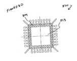
- FIGS. 2 - 4illustrate a cross-section of an IC package according to a first exemplary embodiment of the present invention.
- the IC package 200 of FIG. 2A or 2 Bcomprises a die pad 203 having a first face 203 a and a second face 203 b opposite to the first face.
- first and secondare merely used for convenience and do not reflect the order of formation, placement, or observation.
- a plurality of inner leads 201as shown, each have a first face 201 a , a second face 201 b , and a plurality of sides 201 c (shown in FIG. 4) between the first face 201 a and the second face 102 b .
- the plurality of inner leads 201are disposed substantially co-planar with and substantially around the die pad 203 , as shown in FIG. 4.
- the plurality of inner leads 201may border only two sides of the die pad 203 or may substantially completely encircle the die pad 203 .
- a plurality of outer leads 202as shown, each have a first face 202 a , a second face 202 b , and a plurality of sides 202 c (shown in FIG. 4) between the first face 202 a and the second face 202 b .
- the plurality of outer leads 202are disposed substantially co-planer with and substantially around the plurality of inner leads 201 and the die pad 203 , as shown in FIG. 4.
- the plurality of outer leads 202may border the plurality of inner leads 201 and the die pad 203 on only two sides, or they may substantially completely encircle the plurality of inner leads 201 and the die pad 203 .
- the plurality of sides 202 c of the plurality of outer leads 202may be aligned with the plurality of sides 201 c of the plurality of inner leads 201 , as shown in FIG. 4. In this way, the lead pitch, or effective spacing between one lead and the next becomes zero because the leads effectively overlap with each other.
- the plurality of sides 202 c of the plurality of outer leads 202may be offset from the plurality of sides 201 c of the plurality of inner leads 201 , as shown in FIG. 5, thus creating an effective lead pitch of greater than zero.
- These layoutsenable a higher pin count within a given area of IC package footprint.
- the die pad 203 , the first plurality of leads 201 , and the second plurality of leads 202can be composed of a common copper alloy, such as C194, C7025, C151, or Eftec64T, for example.
- a first adhesive, 204 ais disposed on the first face 203 a of the die pad 203 .
- a second adhesive, 204 bis disposed on the first face 201 a of each of the plurality of inner leads 201 .
- the adhesive used for the adhesive layers 204 a and 204 bmay comprise, for example, electrically conductive or non-conductive epoxy, paste, or adhesive film, or the like as would be understood by those skilled in the art, and are intended to be encompassed here.
- the IC package 200also comprises an IC chip 205 having a first face 205 a and a second face 205 b .
- the second face 205 b of the IC chip 205is coupled to the first face of the die pad 203 a through the first adhesive layer 404 a .
- the second face 205 b of the IC chip 205is further coupled to the first faces 201 a of the plurality of inner leads 201 through the second adhesive layer 204 b .
- This dual coupling of the IC chip 205adds stability to the overall structure of the IC package 200 and also functions to maintain the proper position of the inner leads 201 .
- the IC package 200further comprises a first plurality of wires 211 linking the plurality of inner leads 201 to the IC chip 205 .
- Each of the first plurality of wires 211has a first end 211 a electrically conductively joined to the first face 201 a of one of the plurality of inner leads 201 , and a second end 211 b electrically conductively joined to the first face 205 a of the IC chip 205 .
- the packagealso comprises a second plurality of wires 212 , as shown, each having a first end 212 a electrically conductively joined to the first face 202 a of one of the plurality of outer leads 202 , and a second end 212 b electrically conductively joined to the first face 205 a of the IC chip 205 .
- the first plurality of wires 211 and the second plurality of wires 212can be composed of gold, gold with some level of impurities, aluminum, or copper, for example.
- the goldmay contain 1% impurities. These impurities could include dopants or additives included to improve the properties of the wires as would be understood by one of skill in the art.
- the IC package 200may further comprise an encapsulant 208 .
- the encapsulantmay surround at least the first face 203 a of the die pad 203 , the first faces 201 a of the plurality of inner leads 201 , the first faces 202 a of the plurality of outer leads 202 , the first adhesive layer 204 a , the second adhesive layer 204 b , the first plurality of wires 211 , the second plurality of wires 212 , and the IC chip 205 .
- the encapsulantmay alternatively end before the outer edges of the plurality of leads 202 .
- the encapsulantforms and edge 208 a which leaves a portion 202 d of each of the plurality of leads 202 exposed.
- the encapsulant 208provides overall protection to the elements it surrounds and gives added strength to the package.
- the encapsulantcan be a polymer-based molding compound or any other of many known encapsulant materials as would be understood by one of ordinary skill in the art.
- the IC packagecan further comprise a conductive element 307 having a first face 307 a and a second face 307 b opposite to the first face.
- the conductive element 307is sandwiched with adhesive layers between the die pad 203 and the IC chip 205 .
- the second face 307 b of the conductive element 307is coupled to the first face 203 a of the die pad through the first adhesive layer 204 a and to the first face 201 a of the plurality of inner leads 201 through the second adhesive layer 204 b .
- the first face 307 a of the conductive element 307is coupled to the second face 205 b of the IC chip 205 through a third adhesive layer 304 c .
- the third adhesive layer 304 cmay comprise, for example, electrically conductive or non-conductive epoxy, paste, or adhesive film, or the like as would be understood by one of skill in the art.
- the IC package 300 , 400 , or 500further comprises at least one first linking wire 313 linking the IC chip 205 to the conductive element 307 .
- the at least one first linking wire 313has a first end 313 a electrically conductively joined to the first face 307 a of the conductive element 307 , and a second end 131 b electrically conductively joined to the first face 205 a of the IC chip 205 .
- At least one second linking wire 414(shown in FIG. 4) comprises a first end 414 a electrically conductively joined to the first face 307 a of the conductive element 307 and a second end 414 b electrically conductively joined to the first face 203 a of the die pad 203 .
- the die pad, 203may have at least one lateral portion 203 c , as shown in FIG. 4, which protrudes beyond the conductive element 307 .
- FIG. 6illustrates a cross-section of an IC package 600 according to a second exemplary embodiment of the present invention.
- the IC package 600 of FIG. 6comprises a die pad 203 , a plurality of inner leads 201 , a plurality of outer leads 202 , a first adhesive layer 204 a , a second adhesive layer 204 b , an IC chip 205 , and a first plurality of wires 211 .
- These elementsare described with reference to FIGS. 2 - 5 , and are disposed and interconnected as therein described.
- the IC package 600 of FIG. 6further comprises a third adhesive layer 604 c disposed on the first face 205 a of the IC chip 205 .
- the third adhesive layer 604 cmay comprise, for example, electrically conductive or non-conductive epoxy, paste, or adhesive film, or the like as would be understood by one of skill in the art.
- the IC package 600further comprises a second IC chip 606 having a first face 606 a and a second face 606 b .
- the second face 606 b of the second IC chip 206is connected to the first face 205 a of first IC chip 205 through the third adhesive layer 604 c.
- the IC package 600further comprises a second plurality of wires 212 .
- the second plurality of wireslink the plurality of outer leads 202 to the second IC chip 606 .
- Each of the second plurality of wires 212has a first end 212 a electrically conductively joined to the first face 202 a of one of the plurality of outer leads 202 , and a second end 212 b electrically conductively joined to the first face 606 a of the second IC chip 606 .
- IC package 600can further comprise an encapsulant 208 as described with reference to the first exemplary embodiment and FIGS. 2 and 3.
- the encapsulant 208further surrounds the third adhesive layer 604 c and the second IC chip 606 .
- the die pad 203 , the plurality of inner leads 201 and the plurality of outer leads 212 of the first and second exemplary embodiments of the present inventioncan be formed from leadframe 720 or 820 , respectively.
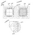
- FIGS. 7 A- 7 Billustrate a leadframe 720 according to a third exemplary embodiment of the present invention.
- Leadframe 720comprises an outer frame portion 725 and a die pad portion 723 .
- the die pad portion 723is substantially centrally disposed with in the outer frame portion 725 .
- the leadframe 720also comprises a plurality of inner lead portions 721 extending substantially radially outward from the central die pad portion 723 .
- the leadframealso comprises a plurality of outer lead portions 722 extending substantially radially inward from said outer frame portion 725 .
- the leadframealso comprises a plurality of tie bars 724 connecting the die pad portion 723 to the outer frame portion 725 .
- the above-mentioned elements of the leadframe 720may be arranged, for example, as illustrated in FIG. 7A or in FIG. 7B, or according to another arrangement as would be understood by one of ordinary skill in the art.
- the leadframe 720can be composed of a common copper alloy, such as C194, C7025, C151, or Eftec64T, for example.
- FIGS. 8A and 9Aillustrate alternate leadframes 820 according to a fourth exemplary embodiment of the present invention.
- leadframe 820comprises an outer frame portion 825 , a die pad portion 823 , a plurality of tie bars 824 connecting the die pad portion 823 to the outer frame portion 825 , and a plurality of protuberances 826 .
- the die pad portion 823is substantially centrally disposed within the outer frame portion 825 .
- the plurality of protuberances 826extend substantially radially inward from the outer frame portion 825 , and each comprises an inner lead portion 827 , an outer lead portion 828 , and a post portion 829 connecting the inner lead portion 827 to the outer lead portion 828 .
- the outer lead portion 828is connected to the outer frame portion 825 .
- the post portion 829has a substantially smaller width than either the inner lead portion 827 or the outer lead portion 828 .
- leadframe 820can be composed of a common copper alloy, such as C194, C7025, C151, or Eftec64T, for example.
- the post portion 829may be straight, such that the plurality of inner lead portions 827 and the plurality of outer lead portions 828 are aligned, and there is an effective lead pitch of zero.
- the post portion 829may be bent, thus creating an offset between the plurality of inner lead portions 827 and the plurality of outer lead portions 828 . According to this aspect, illustrated in FIG. 9A, there is an effective lead pitch of greater than zero, as shown in FIG. 9C.
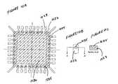
- FIGS. 10 A- 10 Cillustrate a possible aspect of the leadframes according to the third and fourth exemplary embodiments.
- a dimple 1035disposed on a first face of each of the plurality of inner lead portions.
- dimples 1036disposed on a first face of the die pad portion. These dimples may be formed from mechanical or chemical processes. The dimples increase the surface area of the lead portions and the die pad on which an adhesive is disposed, as described with respect to the sixth and seventh embodiments of the present invention, thereby making the connection between the first faces of the inner lead portions of the die pad portion and another element through the adhesive stronger.
- a method of assembling an IC packagecomprises providing a die pad 203 having a first face 203 a and a second face 203 b opposite to the first face; a plurality of inner leads 201 each having a first face 201 a , a second face 201 b opposite to the first face, and a plurality of sides 201 c between the first face and the second face; a plurality of outer leads 202 , each having a first face 202 a , a second face 202 b opposite to the first face, and a plurality of sides 202 c between the first face and the second face, an IC chip 205 having a first face 205 a and a second face 205 b opposite to the first face, and a conductive element 307 having a first face 307 a and a second face 307 b opposite to the first face.
- the methodfurther comprises disposing the inner leads 201 substantially co-planar with and substantially around the die pad 203 , as described with respect to the second exemplary embodiment of the present invention.
- the methodfurther comprises disposing the plurality of outer leads 202 substantially co-planar with and substantially around the inner leads 201 and the die pad 203 , as also described with respect to the second exemplary embodiment of the present invention.
- the sides 201 c of the plurality of inner leads 201 and the sides 202 c of the plurality of outer leadsmay be aligned or offset from each other, as explained with respect to FIGS. 2, 4, and 5 and the first exemplary embodiment of the present invention. This alignment or offsetting allows the effective lead pitch of this embodiment to be zero or greater than zero.
- the method according to the fifth embodiment of the present inventionfurther comprises coupling the second face 307 b of the conductive element 307 to the first face 203 a of the die pad through a first adhesive layer 204 a , and to the first faces 201 a of the plurality of inner leads through a second adhesive layer 204 b .
- the methodalso comprises coupling the second face 205 b of the IC chip to the first face 307 a of the conductive element through a third adhesive layer 304 c .
- the methodalso comprises electrically conductively linking each of the plurality of inner leads 201 to the first face 205 a of the IC chip, each of the plurality of outer leads 202 to the first face 205 a of the IC chip 205 , the first face 205 a of the IC chip to the conductive element 307 , and the conductive element 307 to the die pad 203 .
- the method of assembling an IC packagefurther comprises coupling the second face 203 b of the die pad 203 , the second faces 201 b of the plurality of inner leads 201 , and the second faces 202 b of the plurality of outer leads to a printed circuit board through a fourth adhesive layer.
- the fourth adhesive layercan comprise a conductive adhesive film or an electrically conductive paste, such as, for example, solder paste.
- a method of assembling an IC packagecomprises providing a leadframe 720 having a first face and a second face opposite to the first face.
- the leadframecan be, for example, leadframe 720 of FIG. 7A or alternate leadframe 720 of FIG. 7B.
- FIG. 7AWith exemplary reference to FIG. 7A
- the leadframecomprises an outer frame portion 725 , a die pad portion 723 , a plurality of inner lead portions 721 extending substantially radially outward from the die pad portion 723 , a plurality of outer lead portions 722 extending substantially radially inward from the outer frame portion 725 , and a plurality of tie bars 724 connecting the die pad portion 723 to the outer frame portion 725 .
- the die pad portion 723is substantially centrally disposed within the outer frame portion 725 .
- Each of the inner lead portions 721comprises an inner portion 721 a , a central portion 721 b , and an outer portion 721 c .
- Each of the tie bars 724comprises an inner portion 724 a and an outer portion 724 b .
- the methodalso comprises providing an IC chip 205 having a first face 205 a and a second face 205 b , a first plurality of wires 211 each having a first end 211 a and a second end 211 b , and a second plurality of wires 212 , each having a first end 212 a and a second end 212 b.
- the methodfurther comprises disposing a first adhesive layer 704 on the first face of the leadframe. As illustrated in FIG. 7C, the first adhesive layer 704 covers the die pad portion 723 , the inner portion 721 a and the central portion 721 b of the plurality of inner lead portions 721 , and the inner portion 724 a of the plurality of tie bars 724 . The outer portion 721 c of the plurality of inner lead portions 721 remains free of adhesive.
- the methodfurther comprises severing the outer and central portions 721 b and 721 c from inner portions 721 a and the die pad 723 . This severing can be accomplished mechanically or chemically by cutting slots 730 through the adhesive layer 704 and the inner lead portions 724 , as illustrated in FIG.
- the methodalso comprises mounting the IC chip 205 on the leadframe, whereby the second face 205 b of the IC chip 205 is connected to the first face of the die pad portion 723 and to the first faces of the inner lead portions 724 through adhesive layer 704 .
- This stepprovides stability to the overall IC package and maintains the inner lead portions 724 in their proper positions.
- the methodalso comprises electrically conductively joining the first end 211 a of each of the first plurality of wires 211 to the first face of each of the outer portions 724 c of the plurality of inner lead portions 724 and electrically conductively joining the second end 211 b of each of the first plurality of wires 211 to the first face 205 a of the IC chip 205 .
- the methodalso comprises electrically conductively joining the first end 212 a of each of the second plurality of wires 212 to the first face of each of the plurality of outer lead portions 722 and electrically conductively joining the second end 212 b of each of the second plurality of wires 212 to the first face 205 a of the IC chip 205 .
- a method of assembling an IC packagecomprises providing a leadframe 820 having a first face and a second face opposite to the first face.
- the leadframecomprises an outer frame portion 825 , a die pad portion 823 , a plurality of tie bars 824 connecting the die pad portion 823 to the outer frame portion 825 , and a plurality of protuberances 826 extending substantially radially inward from the outer frame portion 825 .
- the die pad portion 823is substantially centrally disposed within the outer frame portion 825 .
- Each of the plurality of protuberancescomprises an inner lead portion 827 , an outer lead portion 828 , and a post portion 829 connecting the inner lead portion 827 to the outer lead portion 828 the method further comprises providing an IC chip 805 having a first face 805 a and a second face 805 b opposite to the first face, a first plurality of wires 811 each having a first end 811 a and a second end 811 b , and a second plurality of wires 812 each having a first end 812 a and a second end 812 b.
- the methodfurther comprises disposing an adhesive layer 804 on the first face of the leadframe.
- the adhesive layer 804covers the die pad portion 823 , and part of the inner lead portion 827 of each of the plurality of protuberances 826 . Part of each inner lead portion 827 of each of the plurality of protuberances 826 remains free from adhesive 804 .
- the adhesive layer 804can be disposed only on an outer edge of the die pad portion 823 , thereby leaving a central window of the die pad portion 823 free from adhesive.
- the methodfurther comprises mechanically or chemically severing the inner lead portions 827 from the outer lead portions 828 by cutting the post portions 829 .
- the methodalso comprises mounting the IC chip 205 on the leadframe 820 whereby the second face 205 b of the IC chip 205 is connected to the first face of the die pad portion 823 and to the first faces of each of the plurality of inner lead portions 827 through the adhesive layer 804 .
- this stepprovides stability to the overall IC package and maintains the inner lead portions 824 in their proper positions.
- the methodfurther comprises electrically conductively joining the first end 211 a of each of the first plurality of wires 211 to the first face of one of the plurality of inner lead portions 827 and electrically conductively joining the second end 211 b of each of the first plurality of wires 211 to the first face 205 a of the IC chip 205 .
- the methodfurther comprises electrically conductively joining the first end 212 a of each of the second plurality of wires 212 to the first face of one of the plurality of outer lead portions 828 and electrically conductively joining the second end 212 b of each of the second plurality of wires 212 to the first face 205 a of the IC chip 205 .
Landscapes
- Engineering & Computer Science (AREA)
- Computer Hardware Design (AREA)
- Microelectronics & Electronic Packaging (AREA)
- Power Engineering (AREA)
- Physics & Mathematics (AREA)
- Condensed Matter Physics & Semiconductors (AREA)
- General Physics & Mathematics (AREA)
- Lead Frames For Integrated Circuits (AREA)
Abstract
Description
- This application claims the benefit of the co-pending U.S. Provisional Application No. 60/429,315, filed on Nov. 27, 2002, and incorporated herein by reference.[0001]
- 1. Field of the Invention[0002]
- The present invention generally relates to the field of semiconductors. In particular, the present invention relates to an improved high density chip scale leadframe package and a method of assembling the same.[0003]
- 2. Discussion of Related Art[0004]
- Semiconductors are materials that have characteristics of insulators and conductors. In today's technology, semiconductor materials have become extremely important as the basis for transistors, diodes, and other solid-state devices. Semiconductors are usually made from germanium or silicon, but selenium and copper oxide, as well as other materials, are also used. When properly made, semiconductors will conduct electricity in one direction better than they will in the other direction.[0005]
- Semiconductor devices and integrated circuits (ICs) are made up of components, such as transistors and diodes, and elements, such as resistors and capacitors, linked together by conductive connections, to form one or more functional circuits. Interconnects on an IC chip serve the same function as the wiring in a conventional circuit.[0006]
- The input/output functions of an IC are performed by leads which form a link between the IC chip and a substrate. “Lead pitch” is the term given to the spacing between these leads as they are laid out within the IC package. Conventional lead pitch is usually between 1.0 mm and 0.4 mm. as they are laid out within the IC package. Conventional lead pitch is usually between 1.0 mm and 0.4 mm.[0007]
- Emerging electronic product applications are creating a set of challenges for the IC packaging industry.[0008]
- Once the IC chips have been produced and encapsulated in semiconductor packages as described, they may be used in a wide variety of electronic appliances. The variety of these electronic devices utilizing semiconductor packages has grown dramatically in recent years. These devices include cellular phones, portable computers, etc. Each of these devices typically includes a motherboard on which a significant number of such semiconductor packages are secured to provide multiple electronic functions. These electronic appliances are typically manufactured in reduced sizes and at reduced costs, which results in increased consumer demand. It is increasingly desirable, therefore, to reduce the footprint of the semiconductor package so that electronic systems can be incorporated into more compact devices and products.[0009]
- One way to reduce the size of the footprint of IC packages utilizing leadframes is to reduce the lead pitch.[0010]
- An IC package according to the present invention comprises a die pad having a first face and a second face opposite to the first face. The package also comprises a plurality of inner leads, each having a first face, a second face-opposite to the first face, and a plurality of sides between the first face and the second face. The plurality of inner leads is disposed substantially co-planar with, and substantially around, the die pad. The package also comprises a plurality of outer leads having a first face, a second face opposite to the first face, and a plurality of sides between the first face and the second face. The plurality of outer leads is disposed substantially co-planar with, and substantially around, the plurality of inner leads and the die pad. The sides of each of the plurality of outer leads are substantially offset from the sides of each the plurality of inner leads. The package also comprises a first adhesive layer disposed on the first face of the die pad and a second adhesive layer disposed on the first face of each of the plurality of inner leads. The package also comprises an IC chip having a first face and a second face opposite to the first face. The second face of the IC chip is coupled to the first face of the die pad through the first adhesive layer and is further coupled to the first faces of each of the plurality of inner leads through the second adhesive layer. The package further comprises a first plurality of wires linking the plurality of inner leads to the IC chip. Each of the first plurality of wires comprises a first end electrically conductively joined to the first face of one of the plurality of inner leads and a second end electrically conductively joined to the first face of the IC chip. The package further comprises a second plurality of wires linking the plurality of outer leads to the IC chip. Each of the second plurality of wires comprises a first end electrically conductively joined to the first face of one of the plurality of outer leads and a second end electrically conductively joined to the first face of the IC chip.[0011]
- According to one aspect of the first exemplary embodiment, the IC package further comprises an encapsulant which surrounds at least the first face of the die pad, the first faces of the plurality of inner leads, the first faces of the plurality of outer leads, the first adhesive layer, the second adhesive layer, the first plurality of wires, the second plurality of wires, and the IC chip.[0012]
- According to another aspect of the first exemplary embodiment, the IC package further comprises a conductive element having a first face and a second face opposite to the first face. The conductive element is sandwiched between the die pad and the IC chip so that the second face of the conductive element is coupled to the first face of the die pad and further to the first faces of each of the plurality of inner leads, and the first face of the conductive element is coupled to the second face of the IC chip. The package further comprises a first linking wire linking the IC chip to the conductive element and a second linking wire linking the conductive element to the die pad.[0013]
- According to a second exemplary embodiment of the present invention, the IC package comprises a die pad having a first face and a second face opposite to the first face. The package also comprises a plurality of inner leads each having a first face, a second face opposite to the first face, and a plurality of sides between the first face and the second face. The package also comprises a plurality of outer leads, each having a first face, a second face opposite to the first face, and a plurality of sides between the first face and the second face the sides of each of the plurality of outer leads are substantially offset from the sides of each of the plurality of inner leads. The package also comprises a first adhesive layer disposed on the first face of the die pad and a second adhesive layer disposed on the first faces of the plurality of inner leads. The package further comprises a first IC chip having a first face and a second face opposite to the first face. The second face of the first IC chip is coupled to the first face of the die pad through the first adhesive layer and further coupled to the first faces-of the plurality of inner leads through the second adhesive layer. The package further comprises a third adhesive layer disposed on the first face of the first IC chip, and a second IC chip having a first face and a second face opposite to the first face. The second face of the second IC chip is coupled to the first face of the first IC chip through the third adhesive layer. The package also comprises a first plurality of wires linking the plurality of inner leads to the first IC chip, and a second plurality of wires linking the plurality of outer leads to the second IC chip.[0014]
- According to one aspect of the second exemplary embodiment of the present invention, the package further comprises an encapsulant surrounding at least the first face of the die pad, the first faces of the plurality of inner leads, the first faces of the plurality of outer leads, the first adhesive layer, the second adhesive layer, the first IC chip, the third adhesive layer, the second IC chip, the first plurality of wires, and the second plurality of wires.[0015]
- According to a third exemplary embodiment of the present invention, a leadframe for an IC package comprises an outer frame portion, a die pad portion substantially centrally disposed within the outer frame portion, a plurality of inner lead portions extending substantially radially outward from the central die pad portion, a plurality of outer lead portions extending substantially radially inward from said outer frame portion, and a plurality of tie bars connecting the die pad portion to the outer frame portion.[0016]
- According to a fourth exemplary embodiment of the present invention, a leadframe for an IC package comprises an outer frame portion, a die pad portion substantially centrally disposed within the outer frame portion, and a plurality of tie bars connecting the die pad to the outer frame portion. The leadframe further comprises a plurality of protuberances extending substantially radially inward from the outer frame portion. Each of the protuberances comprises an inner lead portion, and outer lead portion, and a post portion connecting the inner lead portion to the outer lead portion. The post portion has a substantially smaller width than either the inner lead portion or the outer lead portion.[0017]
- According to a fifth exemplary embodiment of the present invention, a method of assembling an IC package comprises providing: a die pad having a first face and a second face opposite to the first face; a plurality of inner leads each having a first face and a second face opposite to the first face, and a plurality of sides between the first face and the second face; a plurality of outer leads each having a first face and a second face opposite to the first face, and a plurality of sides between the first face and the second face; an IC chip having a first face and a second face opposite to the first face; and a conductive element having a first face and a second face opposite to the first face. The method further comprises disposing the inner leads substantially co-planar with and substantially around the die pad and disposing the outer leads substantially co-planar with and substantially around the inner leads and the die pad. The plurality of sides of the outer leads are offset from the plurality of sides of the inner leads. The method also comprises coupling the second face of the conductive element to the first face of the die pad through a first adhesive layer, and to the first faces of the plurality of inner leads through a second adhesive layer. The method also comprises coupling the second face of the IC chip to the first face of the conductive element through a third adhesive layer. The method further comprises electrically conductively linking the plurality of inner leads to the first face of the IC chip, the plurality of outer leads to the first face of the IC chip, the first face of the IC chip to the conductive element and the conductive element to the die pad.[0018]
- According to an aspect of the fifth exemplary embodiment of the present invention, the method further comprises coupling the second face of the die pad, the second faces of the plurality of inner leads, and the second faces of the plurality of outer leads to a printed circuit board though a fourth adhesive layer.[0019]
- According to a sixth exemplary embodiment of the present invention, a method of assembling an IC chip comprises providing a leadframe having a first face and a second face opposite to the first face. The leadframe comprises an outer frame portion, a die pad portion substantially centrally disposed within the outer frame portion, a plurality of inner lead portions extending substantially radially outward from the die pad portion, a plurality of outer lead portions extending substantially radially inward from the outer frame portion, and a plurality of tie bars connecting the die pad portion to the outer frame portion. Each of the inner lead portions comprises an inner portion, a central portion, and an outer portion. Each of the tie bars comprises an inner portion and an outer portion. The method also comprises providing an IC chip having a first face and a second face opposite to the first face, a first plurality of wires each having a first end and a second end, and a second plurality of wires each having a first end and a second end. The method also comprises disposing a first adhesive layer on the first face of the leadframe. The first adhesive layer covers the die pad portion, the inner portion and the central portion of the plurality of inner lead portions, and the inner portion of the plurality of tie bars the outer portion of the plurality of inner lead portions remains free from adhesive. The method also comprises severing the outer and central portions of the plurality of inner lead portions from the inner portions of the plurality of inner lead portions and from the die pad portion. The method also comprises mounting the IC chip on the leadframe. The second face of the IC chip is connected to the first face of the die pad portion and to the first faces of each of the plurality of inner lead portions through the first adhesive layer. The method further comprises electrically conductively joining the first end of each of the first plurality of wires to the first face of the outer portion of each of the plurality of inner lead portions, electrically conductively joining the second end of each of the first plurality of wires to the first face of the IC chip, electrically conductively joining the first end of each of the second plurality of wires to the first faces of each of the plurality of outer leads, and electrically conductively joining the second end of the second plurality of wires to the first face of the IC chip.[0020]
- According to a seventh embodiment of the present invention, a method of assembling an IC package comprises providing a leadframe having a first face and a second face opposite to the first face. The leadframe comprises an outer frame portion, a die pad portion substantially centrally disposed within the outer frame portion, a plurality of tie bars connecting the die pad portion to the outer frame portion, and a plurality of protuberances extending substantially radially inward from the outer fame portion. Each of the plurality of protuberances comprises an inner lead portion, an outer lead portion, and a post portion connecting the inner lead portion to the outer lead portion. The method also comprises providing an IC chip having a first face and a second face opposite to the first face, a first plurality of wires each having a first end and a second end, and a second plurality of wires each having a first end and a second end. The method also comprises disposing an adhesive layer on the first face of the leadframe, whereby the adhesive layer covers the die pad portion, and part of the outer lead portion of each of the plurality of protuberances, so that a part of each outer lead portion remains free of adhesive. According to an aspect of the seventh exemplary embodiment of the present invention, the adhesive layer can cover only an outer edge of the die pad portion, thereby leaving a central part of the die pad portion free from adhesive. The method also comprises severing the outer lead portion from the inner lead portion by cutting the post portion. The method also comprises mounting the IC chip on the leadframe, whereby the second face of the IC chip is connected to the first face of the die pad portion and to the first faces of the outer lead portions through the adhesive layer. The method further comprises electrically conductively joining the first end of the first plurality of wires to the first face of the plurality of outer lead portions, the second end of each of the first plurality of wires to the first face of the IC chip, the first end of each of the second plurality of wires to the first face of one of the inner lead portions, and the second end of the second plurality of wires to the first face of the IC chip.[0021]
- These and other features, aspects, and advantages of the present invention will become better understood with reference to the following description, amended claims, and accompanying drawings, which should not be read to limit the invention in any way, in which:[0022]
- FIG. 1 is a cross-section of a conventional IC package.[0023]
- FIG. 2A is a cross-section of an IC package according to a first exemplary embodiment of the present invention.[0024]
- FIG. 2B is an alternative cross-section of an IC package according to a first exemplary embodiment of the present invention.[0025]
- FIG. 3 is a cross section of an IC package according to one aspect of the first exemplary embodiment of the present invention.[0026]
- FIG. 4 is a plane view of the IC package of FIG. 3.[0027]
- FIG. 5 is a plane view of an alternate layout of the IC package of FIG. 3.[0028]
- FIG. 6 is a cross section of an IC package according to a second exemplary embodiment of the present invention.[0029]
- FIGS.[0030]7A-7D are plane views of a leadframe according to a third exemplary embodiment of the present invention.
- FIGS.[0031]8A-8D are plane views of a leadframe according to a fourth exemplary embodiment of the present invention.
- FIGS.[0032]9A-9C are plane views of an alternative leadframe according to a fourth exemplary embodiment of the present invention.
- FIGS.[0033]10A-10C are plane views of an aspect of a leadframe according to a third or fourth exemplary embodiment of the present invention.
- The present invention will be explained in further detail with reference to the accompanying drawings.[0034]
- FIGS.[0035]2-4 illustrate a cross-section of an IC package according to a first exemplary embodiment of the present invention. The
IC package 200 of FIG. 2A or2B comprises adie pad 203 having afirst face 203aand a second face203bopposite to the first face. Hereinafter, the terms “first” and “second” are merely used for convenience and do not reflect the order of formation, placement, or observation. A plurality ofinner leads 201, as shown, each have afirst face 201a, a second face201b, and a plurality of sides201c(shown in FIG. 4) between thefirst face 201aand the second face102b. The plurality ofinner leads 201 are disposed substantially co-planar with and substantially around thedie pad 203, as shown in FIG. 4. The plurality ofinner leads 201 may border only two sides of thedie pad 203 or may substantially completely encircle thedie pad 203. A plurality ofouter leads 202, as shown, each have afirst face 202a, a second face202b, and a plurality of sides202c(shown in FIG. 4) between thefirst face 202aand the second face202b. The plurality ofouter leads 202 are disposed substantially co-planer with and substantially around the plurality ofinner leads 201 and thedie pad 203, as shown in FIG. 4. As with the plurality of inner leads, the plurality ofouter leads 202 may border the plurality ofinner leads 201 and thedie pad 203 on only two sides, or they may substantially completely encircle the plurality ofinner leads 201 and thedie pad 203. The plurality of sides202cof the plurality ofouter leads 202 may be aligned with the plurality of sides201cof the plurality ofinner leads 201, as shown in FIG. 4. In this way, the lead pitch, or effective spacing between one lead and the next becomes zero because the leads effectively overlap with each other. Alternately, the plurality of sides202cof the plurality ofouter leads 202 may be offset from the plurality of sides201cof the plurality ofinner leads 201, as shown in FIG. 5, thus creating an effective lead pitch of greater than zero. These layouts enable a higher pin count within a given area of IC package footprint. Thedie pad 203, the first plurality ofleads 201, and the second plurality ofleads 202 can be composed of a common copper alloy, such as C194, C7025, C151, or Eftec64T, for example. - A first adhesive,[0036]204ais disposed on the
first face 203aof thedie pad 203. A second adhesive,204bis disposed on thefirst face 201aof each of the plurality of inner leads201. The adhesive used for the adhesive layers204aand204bmay comprise, for example, electrically conductive or non-conductive epoxy, paste, or adhesive film, or the like as would be understood by those skilled in the art, and are intended to be encompassed here. - The[0037]
IC package 200 also comprises anIC chip 205 having a first face205aand a second face205b. The second face205bof theIC chip 205 is coupled to the first face of thedie pad 203athrough the first adhesive layer404a. The second face205bof theIC chip 205 is further coupled to the first faces201aof the plurality ofinner leads 201 through the second adhesive layer204b. This dual coupling of theIC chip 205 adds stability to the overall structure of theIC package 200 and also functions to maintain the proper position of the inner leads201. - The[0038]
IC package 200 further comprises a first plurality ofwires 211 linking the plurality ofinner leads 201 to theIC chip 205. Each of the first plurality ofwires 211 has afirst end 211aelectrically conductively joined to thefirst face 201 a of one of the plurality ofinner leads 201, and a second end211belectrically conductively joined to the first face205aof theIC chip 205. The package also comprises a second plurality ofwires 212, as shown, each having a first end212aelectrically conductively joined to thefirst face 202aof one of the plurality ofouter leads 202, and a second end212belectrically conductively joined to the first face205aof theIC chip 205. The first plurality ofwires 211 and the second plurality ofwires 212 can be composed of gold, gold with some level of impurities, aluminum, or copper, for example. For use inwires - According to one aspect of the first exemplary embodiment of the present invention, the[0039]
IC package 200 may further comprise anencapsulant 208. As shown in FIG. 2A, the encapsulant may surround at least thefirst face 203aof thedie pad 203, the first faces201aof the plurality ofinner leads 201, the first faces202aof the plurality ofouter leads 202, the first adhesive layer204a, the second adhesive layer204b, the first plurality ofwires 211, the second plurality ofwires 212, and theIC chip 205. As shown in FIG. 2B, the encapsulant may alternatively end before the outer edges of the plurality of leads202. In this alternative aspect, the encapsulant forms and edge208awhich leaves aportion 202dof each of the plurality ofleads 202 exposed. In both alternatives, theencapsulant 208 provides overall protection to the elements it surrounds and gives added strength to the package. The encapsulant can be a polymer-based molding compound or any other of many known encapsulant materials as would be understood by one of ordinary skill in the art. - With reference to FIGS. 3 and 4 or[0040]5, and according to another aspect of the first exemplary embodiment of the present invention, the IC package can further comprise a
conductive element 307 having a first face307aand a second face307bopposite to the first face. Theconductive element 307 is sandwiched with adhesive layers between thedie pad 203 and theIC chip 205. The second face307bof theconductive element 307 is coupled to thefirst face 203aof the die pad through the first adhesive layer204aand to thefirst face 201aof the plurality ofinner leads 201 through the second adhesive layer204b. The first face307aof theconductive element 307 is coupled to the second face205bof theIC chip 205 through a third adhesive layer304c. As with the first and second adhesive layers204aand204b, the third adhesive layer304cmay comprise, for example, electrically conductive or non-conductive epoxy, paste, or adhesive film, or the like as would be understood by one of skill in the art. - The[0041]
IC package first linking wire 313 linking theIC chip 205 to theconductive element 307. The at least onefirst linking wire 313 has a first end313aelectrically conductively joined to the first face307aof theconductive element 307, and a second end131belectrically conductively joined to the first face205aof theIC chip 205. At least one second linking wire414 (shown in FIG. 4) comprises a first end414aelectrically conductively joined to the first face307aof theconductive element 307 and a second end414belectrically conductively joined to thefirst face 203aof thedie pad 203. For this purpose, the die pad,203 may have at least one lateral portion203c, as shown in FIG. 4, which protrudes beyond theconductive element 307. - FIG. 6 illustrates a cross-section of an[0042]
IC package 600 according to a second exemplary embodiment of the present invention. As described above with reference to FIGS.2-5, theIC package 600 of FIG. 6 comprises adie pad 203, a plurality ofinner leads 201, a plurality ofouter leads 202, a first adhesive layer204a, a second adhesive layer204b, anIC chip 205, and a first plurality ofwires 211. These elements are described with reference to FIGS.2-5, and are disposed and interconnected as therein described. - The[0043]
IC package 600 of FIG. 6 further comprises a third adhesive layer604cdisposed on the first face205aof theIC chip 205. As with the first and second adhesives204aand204b, the third adhesive layer604cmay comprise, for example, electrically conductive or non-conductive epoxy, paste, or adhesive film, or the like as would be understood by one of skill in the art. TheIC package 600 further comprises asecond IC chip 606 having a first face606aand a second face606b. The second face606bof the second IC chip206 is connected to the first face205aoffirst IC chip 205 through the third adhesive layer604c. - As in[0044]
IC package 200, theIC package 600 further comprises a second plurality ofwires 212. According to this embodiment, the second plurality of wires link the plurality ofouter leads 202 to thesecond IC chip 606. Each of the second plurality ofwires 212 has a first end212 a electrically conductively joined to thefirst face 202aof one of the plurality ofouter leads 202, and a second end212belectrically conductively joined to the first face606aof thesecond IC chip 606. - According to one aspect of the second exemplary embodiment of the present invention,[0045]
IC package 600 can further comprise anencapsulant 208 as described with reference to the first exemplary embodiment and FIGS. 2 and 3. According to the present aspect, theencapsulant 208 further surrounds the third adhesive layer604cand thesecond IC chip 606. - With reference to FIGS.[0046]7A-7B,8A, and9A, the
die pad 203, the plurality ofinner leads 201 and the plurality ofouter leads 212 of the first and second exemplary embodiments of the present invention can be formed fromleadframe - FIGS.[0047]7A-7B illustrate a
leadframe 720 according to a third exemplary embodiment of the present invention.Leadframe 720 comprises anouter frame portion 725 and adie pad portion 723. Thedie pad portion 723 is substantially centrally disposed with in theouter frame portion 725. Theleadframe 720 also comprises a plurality ofinner lead portions 721 extending substantially radially outward from the centraldie pad portion 723. The leadframe also comprises a plurality of outerlead portions 722 extending substantially radially inward from saidouter frame portion 725. The leadframe also comprises a plurality of tie bars724 connecting thedie pad portion 723 to theouter frame portion 725. According to the third exemplary embodiment of the present invention, the above-mentioned elements of theleadframe 720 may be arranged, for example, as illustrated in FIG. 7A or in FIG. 7B, or according to another arrangement as would be understood by one of ordinary skill in the art. Theleadframe 720 can be composed of a common copper alloy, such as C194, C7025, C151, or Eftec64T, for example. - FIGS. 8A and 9A illustrate[0048]
alternate leadframes 820 according to a fourth exemplary embodiment of the present invention. With exemplary reference to FIG. 8A,leadframe 820 comprises anouter frame portion 825, adie pad portion 823, a plurality of tie bars824 connecting thedie pad portion 823 to theouter frame portion 825, and a plurality ofprotuberances 826. Thedie pad portion 823 is substantially centrally disposed within theouter frame portion 825. The plurality ofprotuberances 826 extend substantially radially inward from theouter frame portion 825, and each comprises aninner lead portion 827, anouter lead portion 828, and apost portion 829 connecting theinner lead portion 827 to theouter lead portion 828. Theouter lead portion 828 is connected to theouter frame portion 825. Thepost portion 829 has a substantially smaller width than either theinner lead portion 827 or theouter lead portion 828. As withleadframe 720,leadframe 820 can be composed of a common copper alloy, such as C194, C7025, C151, or Eftec64T, for example. As shown in FIG. 8A, thepost portion 829 may be straight, such that the plurality ofinner lead portions 827 and the plurality of outerlead portions 828 are aligned, and there is an effective lead pitch of zero. Alternately, as shown in FIG. 9A, thepost portion 829 may be bent, thus creating an offset between the plurality ofinner lead portions 827 and the plurality of outerlead portions 828. According to this aspect, illustrated in FIG. 9A, there is an effective lead pitch of greater than zero, as shown in FIG. 9C. - FIGS.[0049]10A-10C illustrate a possible aspect of the leadframes according to the third and fourth exemplary embodiments. According to this aspect, there is a
dimple 1035 disposed on a first face of each of the plurality of inner lead portions. There are a plurality ofdimples 1036 disposed on a first face of the die pad portion. These dimples may be formed from mechanical or chemical processes. The dimples increase the surface area of the lead portions and the die pad on which an adhesive is disposed, as described with respect to the sixth and seventh embodiments of the present invention, thereby making the connection between the first faces of the inner lead portions of the die pad portion and another element through the adhesive stronger. - Hereinafter, the elements discussed with respect to the following embodiments and aspects are similar to those discussed with respect to the aforementioned embodiments and aspects and may comprise the same exemplary materials and constructions as discussed above.[0050]
- According to a fifth exemplary embodiment, and with exemplary reference to FIGS. 3 and 4, a method of assembling an IC package comprises providing a[0051]
die pad 203 having afirst face 203aand a second face203bopposite to the first face; a plurality ofinner leads 201 each having afirst face 201a, a second face201bopposite to the first face, and a plurality of sides201cbetween the first face and the second face; a plurality ofouter leads 202, each having afirst face 202a, a second face202bopposite to the first face, and a plurality of sides202cbetween the first face and the second face, anIC chip 205 having a first face205aand a second face205bopposite to the first face, and aconductive element 307 having a first face307aand a second face307bopposite to the first face. The method further comprises disposing the inner leads201 substantially co-planar with and substantially around thedie pad 203, as described with respect to the second exemplary embodiment of the present invention. The method further comprises disposing the plurality ofouter leads 202 substantially co-planar with and substantially around the inner leads201 and thedie pad 203, as also described with respect to the second exemplary embodiment of the present invention. The sides201cof the plurality ofinner leads 201 and the sides202cof the plurality of outer leads may be aligned or offset from each other, as explained with respect to FIGS. 2, 4, and5 and the first exemplary embodiment of the present invention. This alignment or offsetting allows the effective lead pitch of this embodiment to be zero or greater than zero. - The method according to the fifth embodiment of the present invention further comprises coupling the second face[0052]307bof the
conductive element 307 to thefirst face 203aof the die pad through a first adhesive layer204a, and to the first faces201aof the plurality of inner leads through a second adhesive layer204b. The method also comprises coupling the second face205bof the IC chip to the first face307aof the conductive element through a third adhesive layer304c. The method also comprises electrically conductively linking each of the plurality ofinner leads 201 to the first face205aof the IC chip, each of the plurality ofouter leads 202 to the first face205aof theIC chip 205, the first face205aof the IC chip to theconductive element 307, and theconductive element 307 to thedie pad 203. - According to one aspect of the fifth embodiment of the present invention, the method of assembling an IC package further comprises coupling the second face[0053]203bof the
die pad 203, the second faces201bof the plurality ofinner leads 201, and the second faces202bof the plurality of outer leads to a printed circuit board through a fourth adhesive layer. The fourth adhesive layer can comprise a conductive adhesive film or an electrically conductive paste, such as, for example, solder paste. - According to a sixth exemplary embodiment of the present invention, and with exemplary reference to FIGS. 2 and 7A-[0054]7D, a method of assembling an IC package comprises providing a
leadframe 720 having a first face and a second face opposite to the first face. The leadframe can be, for example,leadframe 720 of FIG. 7A oralternate leadframe 720 of FIG. 7B. With exemplary reference to FIG. 7A, the leadframe comprises anouter frame portion 725, adie pad portion 723, a plurality ofinner lead portions 721 extending substantially radially outward from thedie pad portion 723, a plurality of outerlead portions 722 extending substantially radially inward from theouter frame portion 725, and a plurality of tie bars724 connecting thedie pad portion 723 to theouter frame portion 725. - The[0055]
die pad portion 723 is substantially centrally disposed within theouter frame portion 725. Each of theinner lead portions 721 comprises an inner portion721a, a central portion721b, and an outer portion721c. Each of the tie bars724 comprises an inner portion724aand an outer portion724b. The method also comprises providing anIC chip 205 having a first face205aand a second face205b, a first plurality ofwires 211 each having afirst end 211aand a second end211b, and a second plurality ofwires 212, each having a first end212aand a second end212b. - The method further comprises disposing a first[0056]
adhesive layer 704 on the first face of the leadframe. As illustrated in FIG. 7C, the firstadhesive layer 704 covers thedie pad portion 723, the inner portion721aand the central portion721bof the plurality ofinner lead portions 721, and the inner portion724aof the plurality of tie bars724. The outer portion721cof the plurality ofinner lead portions 721 remains free of adhesive. The method further comprises severing the outer and central portions721band721cfrom inner portions721aand thedie pad 723. This severing can be accomplished mechanically or chemically by cuttingslots 730 through theadhesive layer 704 and theinner lead portions 724, as illustrated in FIG. 7D. The method also comprises mounting theIC chip 205 on the leadframe, whereby the second face205bof theIC chip 205 is connected to the first face of thedie pad portion 723 and to the first faces of theinner lead portions 724 throughadhesive layer 704. This step provides stability to the overall IC package and maintains theinner lead portions 724 in their proper positions. The method also comprises electrically conductively joining thefirst end 211aof each of the first plurality ofwires 211 to the first face of each of the outer portions724cof the plurality ofinner lead portions 724 and electrically conductively joining the second end211bof each of the first plurality ofwires 211 to the first face205aof theIC chip 205. The method also comprises electrically conductively joining the first end212aof each of the second plurality ofwires 212 to the first face of each of the plurality of outerlead portions 722 and electrically conductively joining the second end212bof each of the second plurality ofwires 212 to the first face205aof theIC chip 205. - According to a seventh exemplary embodiment of the present invention, and with exemplary reference to FIGS. 2 and 8A-[0057]8D, a method of assembling an IC package comprises providing a
leadframe 820 having a first face and a second face opposite to the first face. The leadframe comprises anouter frame portion 825, adie pad portion 823, a plurality of tie bars824 connecting thedie pad portion 823 to theouter frame portion 825, and a plurality ofprotuberances 826 extending substantially radially inward from theouter frame portion 825. Thedie pad portion 823 is substantially centrally disposed within theouter frame portion 825. Each of the plurality of protuberances comprises aninner lead portion 827, anouter lead portion 828, and apost portion 829 connecting theinner lead portion 827 to theouter lead portion 828 the method further comprises providing an IC chip805 having a first face805aand a second face805bopposite to the first face, a first plurality of wires811 each having a first end811aand a second end811b, and a second plurality of wires812 each having a first end812aand a second end812b. - The method further comprises disposing an[0058]
adhesive layer 804 on the first face of the leadframe. As illustrated in FIG. 8B, theadhesive layer 804 covers thedie pad portion 823, and part of theinner lead portion 827 of each of the plurality ofprotuberances 826. Part of eachinner lead portion 827 of each of the plurality ofprotuberances 826 remains free from adhesive804. According to one aspect of the present embodiment, and as illustrated in FIG. 8D, theadhesive layer 804 can be disposed only on an outer edge of thedie pad portion 823, thereby leaving a central window of thedie pad portion 823 free from adhesive. - As illustrated in FIG. 8C, the method, according to the present embodiment, further comprises mechanically or chemically severing the[0059]
inner lead portions 827 from theouter lead portions 828 by cutting thepost portions 829. The method also comprises mounting theIC chip 205 on theleadframe 820 whereby the second face205bof theIC chip 205 is connected to the first face of thedie pad portion 823 and to the first faces of each of the plurality ofinner lead portions 827 through theadhesive layer 804. As described with respect to the sixth exemplary embodiment of the present invention, this step provides stability to the overall IC package and maintains theinner lead portions 824 in their proper positions. - The method further comprises electrically conductively joining the[0060]
first end 211aof each of the first plurality ofwires 211 to the first face of one of the plurality ofinner lead portions 827 and electrically conductively joining the second end211bof each of the first plurality ofwires 211 to the first face205aof theIC chip 205. The method further comprises electrically conductively joining the first end212aof each of the second plurality ofwires 212 to the first face of one of the plurality of outerlead portions 828 and electrically conductively joining the second end212bof each of the second plurality ofwires 212 to the first face205aof theIC chip 205. - Although the above exemplary embodiments of the present invention have been described, it will be understood by those skilled in the art that the present invention should not be limited to the described exemplary embodiments, but that various changes and modifications can be made within the spirit and scope of the present invention. Accordingly, the scope of the present invention is not limited to the described range of the following claims.[0061]
Claims (26)
Priority Applications (2)
| Application Number | Priority Date | Filing Date | Title |
|---|---|---|---|
| US10/721,382US8129222B2 (en) | 2002-11-27 | 2003-11-26 | High density chip scale leadframe package and method of manufacturing the package |
| US11/205,182US7345357B2 (en) | 2002-11-27 | 2005-08-17 | High density chip scale leadframe package and method of manufacturing the package |
Applications Claiming Priority (2)
| Application Number | Priority Date | Filing Date | Title |
|---|---|---|---|
| US42931502P | 2002-11-27 | 2002-11-27 | |
| US10/721,382US8129222B2 (en) | 2002-11-27 | 2003-11-26 | High density chip scale leadframe package and method of manufacturing the package |
Related Child Applications (1)
| Application Number | Title | Priority Date | Filing Date |
|---|---|---|---|
| US11/205,182DivisionUS7345357B2 (en) | 2002-11-27 | 2005-08-17 | High density chip scale leadframe package and method of manufacturing the package |
Publications (2)
| Publication Number | Publication Date |
|---|---|
| US20040104457A1true US20040104457A1 (en) | 2004-06-03 |
| US8129222B2 US8129222B2 (en) | 2012-03-06 |
Family
ID=32397195
Family Applications (2)
| Application Number | Title | Priority Date | Filing Date |
|---|---|---|---|
| US10/721,382Active2028-12-25US8129222B2 (en) | 2002-11-27 | 2003-11-26 | High density chip scale leadframe package and method of manufacturing the package |
| US11/205,182Expired - Fee RelatedUS7345357B2 (en) | 2002-11-27 | 2005-08-17 | High density chip scale leadframe package and method of manufacturing the package |
Family Applications After (1)
| Application Number | Title | Priority Date | Filing Date |
|---|---|---|---|
| US11/205,182Expired - Fee RelatedUS7345357B2 (en) | 2002-11-27 | 2005-08-17 | High density chip scale leadframe package and method of manufacturing the package |
Country Status (1)
| Country | Link |
|---|---|
| US (2) | US8129222B2 (en) |
Cited By (11)
| Publication number | Priority date | Publication date | Assignee | Title |
|---|---|---|---|---|
| US20060016619A1 (en)* | 2004-07-22 | 2006-01-26 | Samsung Techwin Co., Ltd. | Printed circuit board having structure for relieving stress concentration, and semiconductor chip package equipped with the same |
| US20060055063A1 (en)* | 2004-09-13 | 2006-03-16 | Boulin David M | Leadframe designs for plastic overmold packages |
| US7074654B1 (en)* | 2004-04-21 | 2006-07-11 | Amkor Technology, Inc. | Tape supported memory card leadframe structure |
| US20060214309A1 (en)* | 2004-07-29 | 2006-09-28 | Watkins Charles M | Integrated circuit and methods of redistributing bondpad locations |
| US20070176303A1 (en)* | 2005-12-27 | 2007-08-02 | Makoto Murai | Circuit device |
| US20070187805A1 (en)* | 2006-02-15 | 2007-08-16 | Lee Ming H | COL-TSOP with nonconductive material for reducing package capacitance |
| US20080054421A1 (en)* | 2006-08-23 | 2008-03-06 | Stats Chippac Ltd. | Integrated circuit package system with interlock |
| US20080211069A1 (en)* | 2003-08-05 | 2008-09-04 | Kenji Amano | Semiconductor package configuration with improved lead portion arrangement |
| WO2009059883A1 (en)* | 2007-11-08 | 2009-05-14 | Cambridge Silicon Radio Limited | Chip packaging |
| US20130334686A1 (en)* | 2010-11-26 | 2013-12-19 | Tianshui Huatian Technology Co., Ltd. | Carrier-free land grid array ic chip package and preparation method thereof |
| US20190279941A1 (en)* | 2017-10-20 | 2019-09-12 | Advanced Semiconductor Engineering, Inc. | Semiconductor device package |
Families Citing this family (13)
| Publication number | Priority date | Publication date | Assignee | Title |
|---|---|---|---|---|
| US7556986B1 (en)* | 2004-04-21 | 2009-07-07 | Amkor Technology, Inc. | Tape supported memory card leadframe structure |
| US7598606B2 (en)* | 2005-02-22 | 2009-10-06 | Stats Chippac Ltd. | Integrated circuit package system with die and package combination |
| JP5122172B2 (en)* | 2007-03-30 | 2013-01-16 | ローム株式会社 | Semiconductor light emitting device |
| US20110248392A1 (en)* | 2010-04-12 | 2011-10-13 | Texas Instruments Incorporated | Ball-Grid Array Device Having Chip Assembled on Half-Etched metal Leadframe |
| JP5613463B2 (en)* | 2010-06-03 | 2014-10-22 | ルネサスエレクトロニクス株式会社 | Semiconductor device and manufacturing method thereof |
| JP2012227445A (en) | 2011-04-21 | 2012-11-15 | Renesas Electronics Corp | Semiconductor device and method of manufacturing the same |
| US8455989B2 (en)* | 2011-07-01 | 2013-06-04 | Texas Instruments Incorporated | Package substrate having die pad with outer raised portion and interior recessed portion |
| KR101398016B1 (en)* | 2012-08-08 | 2014-05-30 | 앰코 테크놀로지 코리아 주식회사 | Lead frame package and manufacturing method thereof |
| US8723338B2 (en)* | 2012-08-15 | 2014-05-13 | Stats Chippac Ltd. | Integrated circuit packaging system with array contacts and method of manufacture thereof |
| CN105719975B (en) | 2014-08-15 | 2019-01-08 | 恩智浦美国有限公司 | The floating mould of semiconductor packages |
| US9679831B2 (en) | 2015-08-13 | 2017-06-13 | Cypress Semiconductor Corporation | Tape chip on lead using paste die attach material |
| TWI623076B (en)* | 2016-11-02 | 2018-05-01 | 復盛精密工業股份有限公司 | Method for manufacturing leadframe |
| US11302611B2 (en)* | 2018-11-28 | 2022-04-12 | Texas Instruments Incorporated | Semiconductor package with top circuit and an IC with a gap over the IC |
Citations (51)
| Publication number | Priority date | Publication date | Assignee | Title |
|---|---|---|---|---|
| US4937656A (en)* | 1988-04-22 | 1990-06-26 | Mitsubishi Denki Kabushiki Kaisha | Semiconductor device |
| US4943843A (en)* | 1985-03-25 | 1990-07-24 | Hitachi, Ltd. | Semiconductor device |
| US5234866A (en)* | 1985-03-25 | 1993-08-10 | Hitachi, Ltd. | Semiconductor device and process for producing the same, and lead frame used in said process |
| US5363279A (en)* | 1991-11-14 | 1994-11-08 | Goldstar Electron Co., Ltd. | Semiconductor package for a semiconductor chip having centrally located bottom bond pads |
| US5428248A (en)* | 1992-08-21 | 1995-06-27 | Goldstar Electron Co., Ltd. | Resin molded semiconductor package |
| US5477079A (en)* | 1990-11-13 | 1995-12-19 | Kabushiki Kaisha Toshiba | Power source noise suppressing type semiconductor device |
| US5495398A (en)* | 1992-05-22 | 1996-02-27 | National Semiconductor Corporation | Stacked multi-chip modules and method of manufacturing |
| US5519251A (en)* | 1992-10-20 | 1996-05-21 | Fujitsu Limited | Semiconductor device and method of producing the same |
| US5541446A (en)* | 1994-08-29 | 1996-07-30 | Analog Devices, Inc. | Integrated circuit package with improved heat dissipation |
| US5663594A (en)* | 1994-11-22 | 1997-09-02 | Nec Corporation | Ball grid array type of semiconductor device |
| US5771888A (en)* | 1993-11-22 | 1998-06-30 | Rusch Ag | Tracheal cannula for the mechanical respiration of tracheotomised patients |
| US5780925A (en)* | 1992-10-28 | 1998-07-14 | International Business Machines Corporation | Lead frame package for electronic devices |
| US5789280A (en)* | 1994-10-11 | 1998-08-04 | Motorola, Inc. | Leadframe having secured outer leads, semiconductor device using the leadframe and method of making them |
| US5894108A (en)* | 1997-02-11 | 1999-04-13 | National Semiconductor Corporation | Plastic package with exposed die |
| US5907769A (en)* | 1996-12-30 | 1999-05-25 | Micron Technology, Inc. | Leads under chip in conventional IC package |
| US5977615A (en)* | 1996-12-24 | 1999-11-02 | Matsushita Electronics Corporation | Lead frame, method of manufacturing lead frame, semiconductor device and method of manufacturing semiconductor device |
| US6130115A (en)* | 1996-10-22 | 2000-10-10 | Matsushita Electronics Corporation | Plastic encapsulated semiconductor device and method of manufacturing the same |
| US6166430A (en)* | 1998-05-27 | 2000-12-26 | Matsushita Electronics Corporation | Lead frame, method for manufacturing the frame, resin-molded semiconductor device and method for manufacturing the device |
| US6177718B1 (en)* | 1998-04-28 | 2001-01-23 | Kabushiki Kaisha Toshiba | Resin-sealed semiconductor device |
| US6198171B1 (en)* | 1999-12-30 | 2001-03-06 | Siliconware Precision Industries Co., Ltd. | Thermally enhanced quad flat non-lead package of semiconductor |
| US6229200B1 (en)* | 1998-06-10 | 2001-05-08 | Asat Limited | Saw-singulated leadless plastic chip carrier |
| US6310390B1 (en)* | 1999-04-08 | 2001-10-30 | Micron Technology, Inc. | BGA package and method of fabrication |
| US6399414B1 (en)* | 1999-09-10 | 2002-06-04 | Oki Electric Industry Co., Ltd. | Method for forming semiconductor device |
| US6414385B1 (en)* | 1999-11-08 | 2002-07-02 | Siliconware Precisionindustries Co., Ltd. | Quad flat non-lead package of semiconductor |
| US6433277B1 (en)* | 1998-06-24 | 2002-08-13 | Amkor Technology, Inc. | Plastic integrated circuit package and method and leadframe for making the package |
| US20020109214A1 (en)* | 2001-02-14 | 2002-08-15 | Masanori Minamio | Leadframe, resin-molded semiconductor device including the leadframe, method of making the leadframe and method for manufacturing the device |
| US6437429B1 (en)* | 2001-05-11 | 2002-08-20 | Walsin Advanced Electronics Ltd | Semiconductor package with metal pads |
| US6444498B1 (en)* | 2001-08-08 | 2002-09-03 | Siliconware Precision Industries Co., Ltd | Method of making semiconductor package with heat spreader |
| US20020121650A1 (en)* | 2001-03-01 | 2002-09-05 | Masanori Minamio | Resin-encapsulated semiconductor device and method for manufacturing the same |
| US20020121670A1 (en)* | 2001-03-01 | 2002-09-05 | Matsushita Electric Industrial Co., Ltd. | Lead frame |
| US6455356B1 (en)* | 1998-10-21 | 2002-09-24 | Amkor Technology | Methods for moding a leadframe in plastic integrated circuit devices |
| US20020160552A1 (en)* | 1998-10-21 | 2002-10-31 | Matsushita Electronics Corporation | Terminal land frame and method for manufacturing the same |
| US20030001289A1 (en)* | 2001-06-29 | 2003-01-02 | Matsushita Electric Industrial Co., Ltd. | Resin-sealed semiconductor device and manufacturing method thereof |
| US6552416B1 (en)* | 2000-09-08 | 2003-04-22 | Amkor Technology, Inc. | Multiple die lead frame package with enhanced die-to-die interconnect routing using internal lead trace wiring |
| US6559525B2 (en)* | 2000-01-13 | 2003-05-06 | Siliconware Precision Industries Co., Ltd. | Semiconductor package having heat sink at the outer surface |
| US20030127711A1 (en)* | 2002-01-09 | 2003-07-10 | Matsushita Electric Industrial Co., Ltd. | Lead frame, method for manufacturing the same, resin-encapsulated semiconductor device and method for manufacturing the same |
| US6605865B2 (en)* | 2001-03-19 | 2003-08-12 | Amkor Technology, Inc. | Semiconductor package with optimized leadframe bonding strength |
| US6611047B2 (en)* | 2001-10-12 | 2003-08-26 | Amkor Technology, Inc. | Semiconductor package with singulation crease |
| US6627977B1 (en)* | 2002-05-09 | 2003-09-30 | Amkor Technology, Inc. | Semiconductor package including isolated ring structure |
| US6630371B2 (en)* | 1998-09-03 | 2003-10-07 | Micron Technology, Inc. | Chip on board and heat sink attachment methods |
| US6677663B1 (en)* | 1999-12-30 | 2004-01-13 | Amkor Technology, Inc. | End grid array semiconductor package |
| US6686651B1 (en)* | 2001-11-27 | 2004-02-03 | Amkor Technology, Inc. | Multi-layer leadframe structure |
| US20040021229A1 (en)* | 2002-08-02 | 2004-02-05 | Kinsman Larry D. | Stacked semiconductor package and method producing same |
| US6700189B2 (en)* | 2000-10-10 | 2004-03-02 | Rohm Co., Ltd. | Resin sealed semiconductor device |
| US20040053447A1 (en)* | 2001-06-29 | 2004-03-18 | Foster Donald Craig | Leadframe having fine pitch bond fingers formed using laser cutting method |
| US6713322B2 (en)* | 2001-03-27 | 2004-03-30 | Amkor Technology, Inc. | Lead frame for semiconductor package |
| US6791166B1 (en)* | 2001-04-09 | 2004-09-14 | Amkor Technology, Inc. | Stackable lead frame package using exposed internal lead traces |
| US6798046B1 (en)* | 2002-01-22 | 2004-09-28 | Amkor Technology, Inc. | Semiconductor package including ring structure connected to leads with vertically downset inner ends |
| US6818973B1 (en)* | 2002-09-09 | 2004-11-16 | Amkor Technology, Inc. | Exposed lead QFP package fabricated through the use of a partial saw process |
| US6825062B2 (en)* | 1998-11-20 | 2004-11-30 | Amkor Technology, Inc. | Semiconductor package and method of making using leadframe having lead locks to secure leads to encapsulant |
| US6927478B2 (en)* | 2001-01-15 | 2005-08-09 | Amkor Technology, Inc. | Reduced size semiconductor package with stacked dies |
Family Cites Families (3)
| Publication number | Priority date | Publication date | Assignee | Title |
|---|---|---|---|---|
| JPH0730037A (en)* | 1993-05-11 | 1995-01-31 | Sumitomo Metal Mining Co Ltd | Lead frame |
| KR0179803B1 (en) | 1995-12-29 | 1999-03-20 | 문정환 | Lead Exposure Semiconductor Package |
| US5952711A (en)* | 1996-09-12 | 1999-09-14 | Wohlin; Leslie Theodore | Lead finger immobilization apparatus |
- 2003
- 2003-11-26USUS10/721,382patent/US8129222B2/enactiveActive
- 2005
- 2005-08-17USUS11/205,182patent/US7345357B2/ennot_activeExpired - Fee Related
Patent Citations (77)
| Publication number | Priority date | Publication date | Assignee | Title |
|---|---|---|---|---|
| US4943843A (en)* | 1985-03-25 | 1990-07-24 | Hitachi, Ltd. | Semiconductor device |
| US5234866A (en)* | 1985-03-25 | 1993-08-10 | Hitachi, Ltd. | Semiconductor device and process for producing the same, and lead frame used in said process |
| US4937656A (en)* | 1988-04-22 | 1990-06-26 | Mitsubishi Denki Kabushiki Kaisha | Semiconductor device |
| US5477079A (en)* | 1990-11-13 | 1995-12-19 | Kabushiki Kaisha Toshiba | Power source noise suppressing type semiconductor device |
| US5363279A (en)* | 1991-11-14 | 1994-11-08 | Goldstar Electron Co., Ltd. | Semiconductor package for a semiconductor chip having centrally located bottom bond pads |
| US5495398A (en)* | 1992-05-22 | 1996-02-27 | National Semiconductor Corporation | Stacked multi-chip modules and method of manufacturing |
| US5428248A (en)* | 1992-08-21 | 1995-06-27 | Goldstar Electron Co., Ltd. | Resin molded semiconductor package |
| US5519251A (en)* | 1992-10-20 | 1996-05-21 | Fujitsu Limited | Semiconductor device and method of producing the same |
| US5780925A (en)* | 1992-10-28 | 1998-07-14 | International Business Machines Corporation | Lead frame package for electronic devices |
| US5771888A (en)* | 1993-11-22 | 1998-06-30 | Rusch Ag | Tracheal cannula for the mechanical respiration of tracheotomised patients |
| US5541446A (en)* | 1994-08-29 | 1996-07-30 | Analog Devices, Inc. | Integrated circuit package with improved heat dissipation |
| US5789280A (en)* | 1994-10-11 | 1998-08-04 | Motorola, Inc. | Leadframe having secured outer leads, semiconductor device using the leadframe and method of making them |
| US5663594A (en)* | 1994-11-22 | 1997-09-02 | Nec Corporation | Ball grid array type of semiconductor device |
| US6130115A (en)* | 1996-10-22 | 2000-10-10 | Matsushita Electronics Corporation | Plastic encapsulated semiconductor device and method of manufacturing the same |
| US6225146B1 (en)* | 1996-12-24 | 2001-05-01 | Matsushita Electronics Corporation | Lead frame, method of manufacturing lead frame, semiconductor device and method of manufacturing semiconductor device |
| US5977615A (en)* | 1996-12-24 | 1999-11-02 | Matsushita Electronics Corporation | Lead frame, method of manufacturing lead frame, semiconductor device and method of manufacturing semiconductor device |
| US6277673B1 (en)* | 1996-12-30 | 2001-08-21 | Micron Technology, Inc. | Leads under chip in conventional IC package |
| US20030067059A1 (en)* | 1996-12-30 | 2003-04-10 | Corisis David J. | Leads under chip in conventional IC package |
| US6958528B2 (en)* | 1996-12-30 | 2005-10-25 | Micron Technology, Inc. | Leads under chip IC package |
| US6130474A (en)* | 1996-12-30 | 2000-10-10 | Micron Technology, Inc. | Leads under chip IC package |
| US6445061B2 (en)* | 1996-12-30 | 2002-09-03 | Micron Technology, Inc. | Leads under chip in conventional IC package |
| US5907769A (en)* | 1996-12-30 | 1999-05-25 | Micron Technology, Inc. | Leads under chip in conventional IC package |
| US20020180008A1 (en)* | 1996-12-30 | 2002-12-05 | Corisis David J. | Leads under chip in conventional IC package |
| US20010045629A1 (en)* | 1996-12-30 | 2001-11-29 | Corisis David J. | Leads under chip in conventional IC package |
| US6271580B1 (en)* | 1996-12-30 | 2001-08-07 | Micron Technology, Inc. | Leads under chip in conventional IC package |
| US6830961B2 (en)* | 1996-12-30 | 2004-12-14 | Micron Technology, Inc. | Methods for leads under chip in conventional IC package |
| US20010031553A1 (en)* | 1996-12-30 | 2001-10-18 | Corisis David J. | Leads under chip in conventional IC package |
| US5894108A (en)* | 1997-02-11 | 1999-04-13 | National Semiconductor Corporation | Plastic package with exposed die |
| US6177718B1 (en)* | 1998-04-28 | 2001-01-23 | Kabushiki Kaisha Toshiba | Resin-sealed semiconductor device |
| US6166430A (en)* | 1998-05-27 | 2000-12-26 | Matsushita Electronics Corporation | Lead frame, method for manufacturing the frame, resin-molded semiconductor device and method for manufacturing the device |
| US20010030355A1 (en)* | 1998-06-10 | 2001-10-18 | Mclellan Neil | Saw-singulated leadless plastic chip carrier |
| US6242281B1 (en)* | 1998-06-10 | 2001-06-05 | Asat, Limited | Saw-singulated leadless plastic chip carrier |
| US20020056856A1 (en)* | 1998-06-10 | 2002-05-16 | Mclellan Neil | Saw singulated leadless plastic chip carrier |
| US6229200B1 (en)* | 1998-06-10 | 2001-05-08 | Asat Limited | Saw-singulated leadless plastic chip carrier |
| US20030102537A1 (en)* | 1998-06-10 | 2003-06-05 | Mclellan Neil | Saw singulated leadless plastic chip carrier |
| US6433277B1 (en)* | 1998-06-24 | 2002-08-13 | Amkor Technology, Inc. | Plastic integrated circuit package and method and leadframe for making the package |
| US6630728B2 (en)* | 1998-06-24 | 2003-10-07 | Amkor Technology, Inc. | Plastic integrated circuit package and leadframe for making the package |
| US6684496B2 (en)* | 1998-06-24 | 2004-02-03 | Amkor Technology, Inc. | Method of making an integrated circuit package |
| US6630371B2 (en)* | 1998-09-03 | 2003-10-07 | Micron Technology, Inc. | Chip on board and heat sink attachment methods |
| US6455356B1 (en)* | 1998-10-21 | 2002-09-24 | Amkor Technology | Methods for moding a leadframe in plastic integrated circuit devices |
| US20020160552A1 (en)* | 1998-10-21 | 2002-10-31 | Matsushita Electronics Corporation | Terminal land frame and method for manufacturing the same |
| US6667541B1 (en)* | 1998-10-21 | 2003-12-23 | Matsushita Electric Industrial Co., Ltd. | Terminal land frame and method for manufacturing the same |
| US7026192B2 (en)* | 1998-10-21 | 2006-04-11 | Matsushita Electric Industrial Co. Ltd. | Terminal land frame and method for manufacturing the same |
| US6825062B2 (en)* | 1998-11-20 | 2004-11-30 | Amkor Technology, Inc. | Semiconductor package and method of making using leadframe having lead locks to secure leads to encapsulant |
| US20020192862A1 (en)* | 1999-04-08 | 2002-12-19 | Walter Moden | BGA package and method of fabrication |
| US6310390B1 (en)* | 1999-04-08 | 2001-10-30 | Micron Technology, Inc. | BGA package and method of fabrication |
| US6552427B2 (en)* | 1999-04-08 | 2003-04-22 | Micron Technology, Inc. | BGA package and method of fabrication |
| US6716668B2 (en)* | 1999-09-10 | 2004-04-06 | Oki Electric Industry Co., Ltd. | Method for forming semiconductor device |
| US6399414B1 (en)* | 1999-09-10 | 2002-06-04 | Oki Electric Industry Co., Ltd. | Method for forming semiconductor device |
| US6414385B1 (en)* | 1999-11-08 | 2002-07-02 | Siliconware Precisionindustries Co., Ltd. | Quad flat non-lead package of semiconductor |
| US6677663B1 (en)* | 1999-12-30 | 2004-01-13 | Amkor Technology, Inc. | End grid array semiconductor package |
| US6198171B1 (en)* | 1999-12-30 | 2001-03-06 | Siliconware Precision Industries Co., Ltd. | Thermally enhanced quad flat non-lead package of semiconductor |
| US6559525B2 (en)* | 2000-01-13 | 2003-05-06 | Siliconware Precision Industries Co., Ltd. | Semiconductor package having heat sink at the outer surface |
| US6552416B1 (en)* | 2000-09-08 | 2003-04-22 | Amkor Technology, Inc. | Multiple die lead frame package with enhanced die-to-die interconnect routing using internal lead trace wiring |
| US6700189B2 (en)* | 2000-10-10 | 2004-03-02 | Rohm Co., Ltd. | Resin sealed semiconductor device |
| US6927478B2 (en)* | 2001-01-15 | 2005-08-09 | Amkor Technology, Inc. | Reduced size semiconductor package with stacked dies |
| US6720207B2 (en)* | 2001-02-14 | 2004-04-13 | Matsushita Electric Industrial Co., Ltd. | Leadframe, resin-molded semiconductor device including the leadframe, method of making the leadframe and method for manufacturing the device |
| US20020109214A1 (en)* | 2001-02-14 | 2002-08-15 | Masanori Minamio | Leadframe, resin-molded semiconductor device including the leadframe, method of making the leadframe and method for manufacturing the device |
| US6674154B2 (en)* | 2001-03-01 | 2004-01-06 | Matsushita Electric Industrial Co., Ltd. | Lead frame with multiple rows of external terminals |
| US20020121670A1 (en)* | 2001-03-01 | 2002-09-05 | Matsushita Electric Industrial Co., Ltd. | Lead frame |
| US6710430B2 (en)* | 2001-03-01 | 2004-03-23 | Matsushita Electric Industrial Co., Ltd. | Resin-encapsulated semiconductor device and method for manufacturing the same |
| US20020121650A1 (en)* | 2001-03-01 | 2002-09-05 | Masanori Minamio | Resin-encapsulated semiconductor device and method for manufacturing the same |
| US6605865B2 (en)* | 2001-03-19 | 2003-08-12 | Amkor Technology, Inc. | Semiconductor package with optimized leadframe bonding strength |
| US6713322B2 (en)* | 2001-03-27 | 2004-03-30 | Amkor Technology, Inc. | Lead frame for semiconductor package |
| US6791166B1 (en)* | 2001-04-09 | 2004-09-14 | Amkor Technology, Inc. | Stackable lead frame package using exposed internal lead traces |
| US6437429B1 (en)* | 2001-05-11 | 2002-08-20 | Walsin Advanced Electronics Ltd | Semiconductor package with metal pads |
| US20040053447A1 (en)* | 2001-06-29 | 2004-03-18 | Foster Donald Craig | Leadframe having fine pitch bond fingers formed using laser cutting method |
| US20030001289A1 (en)* | 2001-06-29 | 2003-01-02 | Matsushita Electric Industrial Co., Ltd. | Resin-sealed semiconductor device and manufacturing method thereof |
| US6444498B1 (en)* | 2001-08-08 | 2002-09-03 | Siliconware Precision Industries Co., Ltd | Method of making semiconductor package with heat spreader |
| US6611047B2 (en)* | 2001-10-12 | 2003-08-26 | Amkor Technology, Inc. | Semiconductor package with singulation crease |
| US6686651B1 (en)* | 2001-11-27 | 2004-02-03 | Amkor Technology, Inc. | Multi-layer leadframe structure |
| US20030127711A1 (en)* | 2002-01-09 | 2003-07-10 | Matsushita Electric Industrial Co., Ltd. | Lead frame, method for manufacturing the same, resin-encapsulated semiconductor device and method for manufacturing the same |
| US6798046B1 (en)* | 2002-01-22 | 2004-09-28 | Amkor Technology, Inc. | Semiconductor package including ring structure connected to leads with vertically downset inner ends |
| US6627977B1 (en)* | 2002-05-09 | 2003-09-30 | Amkor Technology, Inc. | Semiconductor package including isolated ring structure |
| US6700206B2 (en)* | 2002-08-02 | 2004-03-02 | Micron Technology, Inc. | Stacked semiconductor package and method producing same |
| US20040021229A1 (en)* | 2002-08-02 | 2004-02-05 | Kinsman Larry D. | Stacked semiconductor package and method producing same |
| US6818973B1 (en)* | 2002-09-09 | 2004-11-16 | Amkor Technology, Inc. | Exposed lead QFP package fabricated through the use of a partial saw process |
Cited By (22)
| Publication number | Priority date | Publication date | Assignee | Title |
|---|---|---|---|---|
| US20080211069A1 (en)* | 2003-08-05 | 2008-09-04 | Kenji Amano | Semiconductor package configuration with improved lead portion arrangement |
| US7579674B2 (en)* | 2003-08-05 | 2009-08-25 | Renesas Technology Corp. | Semiconductor package configuration with improved lead portion arrangement |
| US7074654B1 (en)* | 2004-04-21 | 2006-07-11 | Amkor Technology, Inc. | Tape supported memory card leadframe structure |
| US20060016619A1 (en)* | 2004-07-22 | 2006-01-26 | Samsung Techwin Co., Ltd. | Printed circuit board having structure for relieving stress concentration, and semiconductor chip package equipped with the same |
| US7804693B2 (en)* | 2004-07-22 | 2010-09-28 | Samsung Techwin Co., Ltd. | Printed circuit board having structure for relieving stress concentration, and semiconductor chip package equipped with the same |
| US20060214309A1 (en)* | 2004-07-29 | 2006-09-28 | Watkins Charles M | Integrated circuit and methods of redistributing bondpad locations |
| US20070194458A1 (en)* | 2004-07-29 | 2007-08-23 | Watkins Charles M | Methods of redistributing bondpad locations on an integrated circuit |
| US7795737B2 (en) | 2004-07-29 | 2010-09-14 | Micron Technology, Inc. | Methods of redistributing bondpad locations on an integrated circuit |
| US7566953B2 (en)* | 2004-09-13 | 2009-07-28 | Agere Systems Inc. | Leadframe designs for plastic overmold packages |
| US20060055063A1 (en)* | 2004-09-13 | 2006-03-16 | Boulin David M | Leadframe designs for plastic overmold packages |
| US20060237826A1 (en)* | 2004-09-13 | 2006-10-26 | Boulin David M | Leadframe designs for plastic overmold packages |
| US20070176303A1 (en)* | 2005-12-27 | 2007-08-02 | Makoto Murai | Circuit device |
| US7728411B2 (en)* | 2006-02-15 | 2010-06-01 | Sandisk Corporation | COL-TSOP with nonconductive material for reducing package capacitance |
| US20070187805A1 (en)* | 2006-02-15 | 2007-08-16 | Lee Ming H | COL-TSOP with nonconductive material for reducing package capacitance |
| US20080054421A1 (en)* | 2006-08-23 | 2008-03-06 | Stats Chippac Ltd. | Integrated circuit package system with interlock |
| US7936055B2 (en)* | 2006-08-23 | 2011-05-03 | Stats Chippac Ltd. | Integrated circuit package system with interlock |
| WO2009059883A1 (en)* | 2007-11-08 | 2009-05-14 | Cambridge Silicon Radio Limited | Chip packaging |
| US8508032B2 (en) | 2007-11-08 | 2013-08-13 | Cambridge Silicon Radio Limited | Chip packaging |
| US20130334686A1 (en)* | 2010-11-26 | 2013-12-19 | Tianshui Huatian Technology Co., Ltd. | Carrier-free land grid array ic chip package and preparation method thereof |
| US9136231B2 (en)* | 2010-11-26 | 2015-09-15 | Tianshui Huatian Technology Co., Ltd. | Carrier-free land grid array IC chip package and preparation method thereof |
| US20190279941A1 (en)* | 2017-10-20 | 2019-09-12 | Advanced Semiconductor Engineering, Inc. | Semiconductor device package |
| US10797004B2 (en)* | 2017-10-20 | 2020-10-06 | Advanced Semiconductor Engineering, Inc. | Semiconductor device package |
Also Published As
| Publication number | Publication date |
|---|---|
| US8129222B2 (en) | 2012-03-06 |
| US7345357B2 (en) | 2008-03-18 |
| US20050275077A1 (en) | 2005-12-15 |
Similar Documents
| Publication | Publication Date | Title |
|---|---|---|
| US8129222B2 (en) | High density chip scale leadframe package and method of manufacturing the package | |
| US7323769B2 (en) | High performance chip scale leadframe package with thermal dissipating structure and annular element and method of manufacturing package | |
| US7737537B2 (en) | Electronic device | |
| US6781240B2 (en) | Semiconductor package with semiconductor chips stacked therein and method of making the package | |
| US7473584B1 (en) | Method for fabricating a fan-in leadframe semiconductor package | |
| US7834436B2 (en) | Semiconductor chip package | |
| US20020014689A1 (en) | Multiple stacked-chip packaging structure | |
| CN101350318B (en) | Electronic package and electronic device | |
| US7202554B1 (en) | Semiconductor package and its manufacturing method | |
| JP5051463B2 (en) | Stacked package integrated circuit device manufacturing method | |
| KR101440933B1 (en) | Integrated circuit package system employing bump technology | |
| CN102842557A (en) | A packaging structure and manufacturing method thereof | |
| US20050006730A1 (en) | Semiconductor component and method of manufacturing same | |
| US8072050B1 (en) | Semiconductor device with increased I/O leadframe including passive device | |
| US7109570B2 (en) | Integrated circuit package with leadframe enhancement and method of manufacturing the same | |
| US7307352B2 (en) | Semiconductor package having changed substrate design using special wire bonding | |
| US7102211B2 (en) | Semiconductor device and hybrid integrated circuit device | |
| US7851899B2 (en) | Multi-chip ball grid array package and method of manufacture | |
| TW200933868A (en) | Stacked chip package structure | |
| TWI338927B (en) | Multi-chip ball grid array package and method of manufacture | |
| KR100437821B1 (en) | semiconductor package and metod for fabricating the same | |
| TW200929494A (en) | Leadframe package and leadframe | |
| KR20040013736A (en) | Method of manufacturing semiconductor package | |
| JP3491606B2 (en) | Semiconductor device and manufacturing method thereof | |
| TW202510243A (en) | Package |
Legal Events
| Date | Code | Title | Description |
|---|---|---|---|
| AS | Assignment | Owner name:UNITED TEST AND ASSEMBLY TEST CENTER LTD., SINGAPO Free format text:ASSIGNMENT OF ASSIGNORS INTEREST;ASSIGNORS:TAN, HIEN BOON;SUN, ANTHONY YI SHENG;REEL/FRAME:014744/0665 Effective date:20031121 | |
| AS | Assignment | Owner name:JPMORGAN CHASE BANK, N.A., TEXAS Free format text:SECURITY AGREEMENT;ASSIGNOR:UNITED TEST AND ASSEMBLY CENTER LTD.;REEL/FRAME:020072/0018 Effective date:20071030 Owner name:JPMORGAN CHASE BANK, N.A.,TEXAS Free format text:SECURITY AGREEMENT;ASSIGNOR:UNITED TEST AND ASSEMBLY CENTER LTD.;REEL/FRAME:020072/0018 Effective date:20071030 | |
| AS | Assignment | Owner name:JPMORGAN CHASE BANK, N.A., TEXAS Free format text:SECURITY AGREEMENT;ASSIGNOR:UNITED TEST AND ASSEMBLY CENTER LTD.;REEL/FRAME:020866/0116 Effective date:20080425 Owner name:JPMORGAN CHASE BANK, N.A.,TEXAS Free format text:SECURITY AGREEMENT;ASSIGNOR:UNITED TEST AND ASSEMBLY CENTER LTD.;REEL/FRAME:020866/0116 Effective date:20080425 | |
| STCF | Information on status: patent grant | Free format text:PATENTED CASE | |
| FEPP | Fee payment procedure | Free format text:PAYOR NUMBER ASSIGNED (ORIGINAL EVENT CODE: ASPN); ENTITY STATUS OF PATENT OWNER: LARGE ENTITY | |
| FPAY | Fee payment | Year of fee payment:4 | |
| AS | Assignment | Owner name:UTAC HEADQUARTERS PTE. LTD., SINGAPORE Free format text:ASSIGNMENT OF ASSIGNORS INTEREST;ASSIGNOR:UNITED TEST AND ASSEMBLY CENTER LIMITED;REEL/FRAME:037959/0822 Effective date:20150508 | |
| AS | Assignment | Owner name:UTAC HEADQUARTERS PTE. LTD., SINGAPORE Free format text:CORRECTIVE ASSIGNMENT TO CORRECT THE TO ADD THE ANNEX A AND THE ANNEX B WHICH WAS INADVERTENTLY LEFTOUT IN THE ORIGINAL ASSIGNMENT DOCUMENT PREVIOUSLY RECORDED ON REEL 037959 FRAME 0822. ASSIGNOR(S) HEREBY CONFIRMS THE ASSIGNMENT;ASSIGNOR:UNITED TEST AND ASSEMBLY CENTER LIMITED;REEL/FRAME:039885/0541 Effective date:20150508 | |
| AS | Assignment | Owner name:UTAC HEADQUARTERS PTE. LTD., SINGAPORE Free format text:CORRECTIVE ASSIGNMENT TO CORRECT THE INCLUDE PATENT NUMBER 8816482 PREVIOUSLY RECORDED AT REEL: 039885 FRAME: 0541. ASSIGNOR(S) HEREBY CONFIRMS THE ASSIGNMENT;ASSIGNOR:UNITED TEST AND ASSEMBLY CENTER LIMITED;REEL/FRAME:043979/0820 Effective date:20150508 | |
| AS | Assignment | Owner name:UNITED TEST AND ASSEMBLY CENTER LTD., SINGAPORE Free format text:RELEASE BY SECURED PARTY;ASSIGNOR:JPMORGAN CHASE BANK, N.A.;REEL/FRAME:044549/0152 Effective date:20130207 | |
| MAFP | Maintenance fee payment | Free format text:PAYMENT OF MAINTENANCE FEE, 8TH YEAR, LARGE ENTITY (ORIGINAL EVENT CODE: M1552); ENTITY STATUS OF PATENT OWNER: LARGE ENTITY Year of fee payment:8 | |
| MAFP | Maintenance fee payment | Free format text:PAYMENT OF MAINTENANCE FEE, 12TH YEAR, LARGE ENTITY (ORIGINAL EVENT CODE: M1553); ENTITY STATUS OF PATENT OWNER: LARGE ENTITY Year of fee payment:12 |