US20040104197A1 - Evaporation mask, method of fabricating organic electroluminescent device using the same, and organic electroluminescent device - Google Patents
Evaporation mask, method of fabricating organic electroluminescent device using the same, and organic electroluminescent deviceDownload PDFInfo
- Publication number
- US20040104197A1 US20040104197A1US10/718,640US71864003AUS2004104197A1US 20040104197 A1US20040104197 A1US 20040104197A1US 71864003 AUS71864003 AUS 71864003AUS 2004104197 A1US2004104197 A1US 2004104197A1
- Authority
- US
- United States
- Prior art keywords
- apertures
- mask
- dummy
- organic
- main
- Prior art date
- Legal status (The legal status is an assumption and is not a legal conclusion. Google has not performed a legal analysis and makes no representation as to the accuracy of the status listed.)
- Granted
Links
Images


Classifications
- H—ELECTRICITY
- H05—ELECTRIC TECHNIQUES NOT OTHERWISE PROVIDED FOR
- H05B—ELECTRIC HEATING; ELECTRIC LIGHT SOURCES NOT OTHERWISE PROVIDED FOR; CIRCUIT ARRANGEMENTS FOR ELECTRIC LIGHT SOURCES, IN GENERAL
- H05B33/00—Electroluminescent light sources
- H05B33/10—Apparatus or processes specially adapted to the manufacture of electroluminescent light sources
- C—CHEMISTRY; METALLURGY
- C23—COATING METALLIC MATERIAL; COATING MATERIAL WITH METALLIC MATERIAL; CHEMICAL SURFACE TREATMENT; DIFFUSION TREATMENT OF METALLIC MATERIAL; COATING BY VACUUM EVAPORATION, BY SPUTTERING, BY ION IMPLANTATION OR BY CHEMICAL VAPOUR DEPOSITION, IN GENERAL; INHIBITING CORROSION OF METALLIC MATERIAL OR INCRUSTATION IN GENERAL
- C23C—COATING METALLIC MATERIAL; COATING MATERIAL WITH METALLIC MATERIAL; SURFACE TREATMENT OF METALLIC MATERIAL BY DIFFUSION INTO THE SURFACE, BY CHEMICAL CONVERSION OR SUBSTITUTION; COATING BY VACUUM EVAPORATION, BY SPUTTERING, BY ION IMPLANTATION OR BY CHEMICAL VAPOUR DEPOSITION, IN GENERAL
- C23C14/00—Coating by vacuum evaporation, by sputtering or by ion implantation of the coating forming material
- C23C14/04—Coating on selected surface areas, e.g. using masks
- C23C14/042—Coating on selected surface areas, e.g. using masks using masks
- C—CHEMISTRY; METALLURGY
- C23—COATING METALLIC MATERIAL; COATING MATERIAL WITH METALLIC MATERIAL; CHEMICAL SURFACE TREATMENT; DIFFUSION TREATMENT OF METALLIC MATERIAL; COATING BY VACUUM EVAPORATION, BY SPUTTERING, BY ION IMPLANTATION OR BY CHEMICAL VAPOUR DEPOSITION, IN GENERAL; INHIBITING CORROSION OF METALLIC MATERIAL OR INCRUSTATION IN GENERAL
- C23C—COATING METALLIC MATERIAL; COATING MATERIAL WITH METALLIC MATERIAL; SURFACE TREATMENT OF METALLIC MATERIAL BY DIFFUSION INTO THE SURFACE, BY CHEMICAL CONVERSION OR SUBSTITUTION; COATING BY VACUUM EVAPORATION, BY SPUTTERING, BY ION IMPLANTATION OR BY CHEMICAL VAPOUR DEPOSITION, IN GENERAL
- C23C14/00—Coating by vacuum evaporation, by sputtering or by ion implantation of the coating forming material
- C23C14/06—Coating by vacuum evaporation, by sputtering or by ion implantation of the coating forming material characterised by the coating material
- C23C14/12—Organic material
- H—ELECTRICITY
- H10—SEMICONDUCTOR DEVICES; ELECTRIC SOLID-STATE DEVICES NOT OTHERWISE PROVIDED FOR
- H10K—ORGANIC ELECTRIC SOLID-STATE DEVICES
- H10K59/00—Integrated devices, or assemblies of multiple devices, comprising at least one organic light-emitting element covered by group H10K50/00
- H10K59/80—Constructional details
- H10K59/88—Dummy elements, i.e. elements having non-functional features
- H—ELECTRICITY
- H10—SEMICONDUCTOR DEVICES; ELECTRIC SOLID-STATE DEVICES NOT OTHERWISE PROVIDED FOR
- H10K—ORGANIC ELECTRIC SOLID-STATE DEVICES
- H10K71/00—Manufacture or treatment specially adapted for the organic devices covered by this subclass
- H—ELECTRICITY
- H10—SEMICONDUCTOR DEVICES; ELECTRIC SOLID-STATE DEVICES NOT OTHERWISE PROVIDED FOR
- H10K—ORGANIC ELECTRIC SOLID-STATE DEVICES
- H10K71/00—Manufacture or treatment specially adapted for the organic devices covered by this subclass
- H10K71/10—Deposition of organic active material
- H10K71/16—Deposition of organic active material using physical vapour deposition [PVD], e.g. vacuum deposition or sputtering
- H10K71/166—Deposition of organic active material using physical vapour deposition [PVD], e.g. vacuum deposition or sputtering using selective deposition, e.g. using a mask
- G—PHYSICS
- G03—PHOTOGRAPHY; CINEMATOGRAPHY; ANALOGOUS TECHNIQUES USING WAVES OTHER THAN OPTICAL WAVES; ELECTROGRAPHY; HOLOGRAPHY
- G03F—PHOTOMECHANICAL PRODUCTION OF TEXTURED OR PATTERNED SURFACES, e.g. FOR PRINTING, FOR PROCESSING OF SEMICONDUCTOR DEVICES; MATERIALS THEREFOR; ORIGINALS THEREFOR; APPARATUS SPECIALLY ADAPTED THEREFOR
- G03F1/00—Originals for photomechanical production of textured or patterned surfaces, e.g., masks, photo-masks, reticles; Mask blanks or pellicles therefor; Containers specially adapted therefor; Preparation thereof
- G03F1/20—Masks or mask blanks for imaging by charged particle beam [CPB] radiation, e.g. by electron beam; Preparation thereof
- H—ELECTRICITY
- H10—SEMICONDUCTOR DEVICES; ELECTRIC SOLID-STATE DEVICES NOT OTHERWISE PROVIDED FOR
- H10K—ORGANIC ELECTRIC SOLID-STATE DEVICES
- H10K59/00—Integrated devices, or assemblies of multiple devices, comprising at least one organic light-emitting element covered by group H10K50/00
- H10K59/10—OLED displays
- H10K59/17—Passive-matrix OLED displays
Definitions
- the present inventionrelates to an evaporation mask, and, more particularly, to an evaporation mask in which the pitch between adjacent apertures can be kept even when a tension is applied, a method of fabricating an organic electroluminescent (EL) device using the evaporation mask, and an organic EL device manufactured using the above method.
- ELorganic electroluminescent
- EL deviceswhich are spontaneous light-emitting display devices, provide a wide viewing angle, good contrast, and a high response speed. Accordingly, much attention is being focused on EL devices because they can be used as a next-generation display device.
- EL devicesare classified as inorganic EL devices or organic EL devices, depending on what material is used to form a light-emitting layer.
- Organic EL deviceshave a higher brightness and faster responsivity than inorganic EL devices, and can provide color display, so they are presently being more actively developed.
- Organic EL devicesinclude first electrodes formed in a predetermined pattern on a transparent insulating substrate, an organic film formed on the first electrodes by vacuum evaporation, and second electrodes formed on the organic film such that the first and second electrodes cross each other.
- the first electrodesare typically formed by patterning indium tin oxide (ITO) using a photolithographic method.
- ITOindium tin oxide
- Such a photolithographic methodcan be used before an organic film is formed, but causes a problem when it is used after an organic film is formed. Because the organic film is very sensitive to water, it must be thoroughly isolated from water both while being fabricated and after the fabrication. Consequently, a photolithographic method including an exposure to water during pealing-off and etching of a resist is not suitable for patterning the organic film and the second electrode layer.
- This problemis usually solved by vacuum-depositing an organic light emissive material for the organic film and a material for the second electrode layer using a patterned mask.
- the second electrode layercan be patterned using a cathode separator, but it is known that a vacuum evaporation method using an evaporation mask is the most appropriate way to pattern a low molecular organic film.
- a technique of patterning an organic film or a second electrode layer using a maskis very important in the manufacture of full-color organic EL devices.
- Examples of conventional full-color organic EL device coloring methodsinclude a three-color independent evaporation method, in which red (R), green (G), and blue (B) color pixels are independently deposited on a substrate, a color conversion method (CCM), in which a color conversion layer is formed on a light emissive surface using a blue light source, and a color filtering method, which uses a white light source and a color filter.
- the three-color independent evaporation methodhas attracted much attention because it is simple to perform, and provides a high color purity and efficiency.
- the R, G, and B color pixelsare independently deposited on a substrate using an evaporation mask.
- the evaporation maskmust be made of a material with a low thermal expansion coefficient in order to prevent thermal deformation, and also must be magnetic if the evaporation mask is to be adhered to the substrate using a magnet. More importantly, the evaporation mask must be highly accurate. In particular, the positions of deposited pixels, that is, the widths of pattern apertures, must be highly accurate, and a high accuracy of a total mask pitch is also required.
- an organic EL devicemust have a high fineness of 130 ppi or greater and an aperture efficiency of 50% or greater, deviation in the widths of apertures of the evaporation mask must not exceed ⁇ 5 ⁇ m, and deviation in the total mask pitch must not exceed ⁇ 10 ⁇ m.
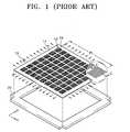
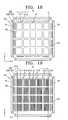
- an evaporation mask 10 used to deposit an organic film or electrodes when fabricating an organic EL deviceis typically supported by a frame 20 , so that the evaporation mask 10 is drawn taut.
- a plurality of mask units 12allowing a single organic EL device to be formed thereon, are formed on a single metal thin plate 11 .
- the evaporation mask 10is thinly formed and minutely patterned, if it is used without any treatment, some parts of it may droop, preventing accurate patterning. Accordingly, as shown in FIG. 1, optimal tension in the x- and y-axis directions is applied to the evaporation mask 10 to obtain a predetermined accuracy of a total pitch (Pt), and the taut evaporation mask 10 is coupled to the mask frame 20 . Upon coupling, it is important to not change the Pt accuracy.
- the coupling of the evaporation mask 10 to the mask frame 20can be achieved by various methods such as using an adhesive, laser welding, or resistance welding.
- Each of the mask units 12includes a pattern of apertures. As shown in FIG. 1, each of the mask units 12 may have strip-like apertures elongated in the y-axis direction. However, the tension makes it difficult for the outermost apertures of each of the mask units 12 to maintain a predetermined level of accuracy.
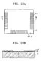
- FIG. 2is a cross-section of a mask unit 12 taken along line I-I of FIG. 1, which shows apertures 13 formed in the mask unit 12 .
- a shielding portion 14is provided between adjacent apertures 13 , and outermost apertures 13 a are each defined by a shield portion 14 and a rib 15 between adjacent mask units.
- an edge portion 15 a of the rib 15may curve upward. Such deformation of the edge portion 15 a of the rib 15 degrades the accuracy of the widths of each of the outermost apertures 13 a . Hence, the accuracy of deposition performed on an organic emissive film through the outermost apertures 13 a is degraded, and, consequently, accurate patterning of the organic emissive film is not accomplished outside a panel. If an edge of a rib between adjacent mask units is deformed, the deformed rib contacts the organic emissive film, thus generating a defect such as a dark point or a pixel short-circuit on the perimeter of a panel.
- mask units 12 a and 12 b located at the outermost sides in the direction perpendicular to the direction of the length of apertures 13 , that is, in the x-axis direction where tension is appliedmay be deformed more seriously than other mask units 12 due to the tension applied in the x-axis direction. Accordingly, the accuracy of a total pitch (Pt), the gap between a line 16 a connecting the edges of the outer ribs of the mask units 12 a and a line 16 b connecting the edges of the outer ribs of the mask units 12 b , decreases, resulting in degradation of the accuracy of patterning of the mask units 12 .
- Pttotal pitch
- a mask that overcomes the problem of the deformation of strips that form slits due to thermal expansion of the maskis disclosed in Japanese Patent Publication No. 2001-247961.
- the disclosed maskincludes a mask portion and a screen portion.
- the mask portionis an evaporation mask used to form a patterning film on a substrate by evaporation, and has partitions for defining a plurality of first apertures.
- the screen portioncontains a magnetic material and has a plurality of second apertures smaller than the first apertures. The second apertures are disposed on the first apertures of the mask portion.
- Japanese Patent Publication No. 2001-273979discloses the structure of a magnetic mask.
- Japanese Patent Publication No. 2001-254169discloses an evaporation mask frame assembly in which a patterned mask masks a deposition area while adhering closely to a material to be deposited, and has fine gaps and fine patterns. The fine patterns of the patterned mask are supported by fine ribs.
- Japanese Patent Publication No. 2002-9098discloses a pattern forming apparatus for preventing a pre-formed film on a substrate from being damaged due to a mask coming partially off of a frame due to a thermal expansion during evaporation.
- the pattern forming apparatusincludes a support which is formed to be larger than the mask, and has a dent portion onto which the mask is seated.
- the supportprevents a mask from becoming rippled due to thermal expansion during the formation of a film.
- the magnetic elementmakes the mask closer to the substrate so that a space between the mask and the support is created. This space contributes to cooling the mask.
- the disclosed mask having slitsis not firmly supported by the frame, the location of the mask cannot be accurately controlled.
- the location of the evaporation maskmay be changed during evaporation.
- Japanese Patent Publication No. 2002-8859discloses a pattern forming apparatus for preventing a mask from being expanded by heat during the formation of a film, in which a liquid path is formed within a frame which supports the mask, and a cooling solution circulates within the liquid path.
- this inventionalso overlooks the possibility of tensions and apertures becoming inaccurate during fixation of the mask into the frame.
- Japanese Patent Publication Nos. 2000-48954, 2000-173769, 2001-203079, and 2001-110567disclose metal masks including supplementary lines to prevent drooping of a mask shield between the mask and a frame. Like the above-disclosed masks, these masks may be stretched and warped while being fixed onto a frame after applying tension in order to accomplish highly accurate patterning.
- the present inventionprovides an evaporation mask that reduces deviation of patterns by reducing variation in the accuracy of the widths of apertures that may be caused by supporting a taut evaporation mask, a method of manufacturing an organic EL device using the evaporation mask, and an organic EL device manufactured by the method.
- the present inventionalso provides an evaporation mask that improves pattern accuracy by compensating for a total pitch when tension is applied to the evaporation mask, a method of manufacturing an organic EL device using the evaporation mask, and an organic EL device manufactured by the method.
- an evaporation maskformed of a thin film, wherein the evaporation mask is drawn taut by application of tension and comprises at least one mask unit.
- the mask unitincludes a plurality of main apertures and a plurality of first dummy apertures formed adjacent to outermost ones of the main apertures in a direction in which tension is applied to the evaporation mask.
- the main aperturesmay form an effective deposition area, and the first dummy apertures may form an ineffective deposition area.
- At least one of the first dummy aperturesmay be formed parallel to the main apertures, and at least another one of the first dummy apertures may be formed perpendicular to the main apertures.
- the evaporation maskmay comprise at least two mask units, and may further comprise a plurality of second dummy apertures formed outside and adjacent to the outermost mask units in the direction in which tension is applied to the evaporation mask.
- the second dummy aperturesmay be formed outside the effective deposition areas where the mask units are formed.
- At least one of the second dummy aperturesmay be formed parallel to the main apertures of the mask units, and at least another one of the second dummy apertures may be formed perpendicular to the main apertures.
- evaporation maskformed of a thin film, wherein the evaporation mask is drawn taut by application of tension.
- the evaporation maskincludes at least two mask units each having at least one main aperture and at least one second dummy aperture formed outside and adjacent to the mask units located at the outermost sides in the direction in which tension is applied to the evaporation mask.
- the at least one main aperture of each of the mask unitsmay be used to form an effective deposition area, and the at least one second dummy aperture may be formed outside of the effective deposition areas where the mask units are formed.
- the at least one second dummy aperturemay comprise at least two second dummy apertures, wherein at least one of the second dummy apertures may be formed parallel to the at least one main aperture of the mask units, and at least another one of the second dummy apertures may be formed perpendicular to the at least one main aperture.
- an organic electroluminescent (EL) deviceIn this method, first electrodes are formed on a substrate. Next, an evaporation mask to form an organic film is disposed over the substrate.
- the evaporation maskis drawn taut by application of tension and has at least one mask unit.
- the mask unitcomprises a plurality of main apertures and a plurality of first dummy apertures formed adjacent to outmost main apertures in a direction in which tension is applied to the evaporation mask.
- the organic filmcomprises an effective luminescent area formed to cover at least the first electrodes by evaporating an organic material containing an organic luminescent material through the main apertures.
- a first dummy pattern areais formed outside the effective luminescent area through the first dummy apertures.
- second electrodesare formed on the organic film so that the effective luminescent area is formed at an area where the first and second electrodes overlap. Finally, the resulting structure is sealed.
- At least one of the first dummy aperturesmay be formed parallel to the main apertures, and at least another one of the first dummy apertures may be formed perpendicular to the main apertures.
- At least two organic EL devicesmay be manufactured in a single process, and the evaporation mask may comprise at least two mask units, through each of which the organic film of a single organic EL device can be deposited, and a plurality of second dummy apertures outside and adjacent to outermost ones of the mask units in the direction in which tension is applied to the evaporation mask.
- the second dummy apertures of the evaporation maskmay be located outside the effective luminescent areas of the organic EL devices that may be deposited by the outermost mask units adjacent to the second dummy apertures.
- At least one of the second dummy aperturesmay be formed parallel to the main apertures of the mask units, and at least one of the second dummy apertures may be formed perpendicular to the main apertures.
- an evaporation mask to form the second electrodesmay be disposed over the substrate.
- the evaporation maskis drawn taut by application of tension and has at least one mask unit.
- the mask unitcomprises a plurality of main apertures and a plurality of first dummy apertures formed adjacent to the outermost main apertures in the direction in which tension is applied to the evaporation mask.
- the second electrodesmay be formed on the effective luminescent area through the main apertures, and a second dummy pattern area may be formed outside the effective luminescent area through the first dummy apertures.
- At least one of the first dummy aperturesmay be formed parallel to the main apertures, and at least another one of the first dummy apertures may be formed perpendicular to the main apertures.
- At least two organic EL devicesmay be manufactured in a single process.
- the evaporation maskmay comprise at least two mask units, through each of which the second electrodes of a single organic EL device can be deposited, and a plurality of second dummy apertures outside and adjacent to the outermost mask units in the direction in which tension is applied to the evaporation mask.
- the second dummy aperturesmay be located outside the effective luminescent areas of the organic EL devices that are deposited by the outermost mask units adjacent to the second dummy apertures.
- At least one of the second dummy aperturesmay be formed parallel to the main apertures of the mask units, and at least another one of the second dummy apertures may be formed perpendicular to the main apertures.
- At least two organic EL devicesmay be manufactured in a single process.
- the second electrodesmay be formed using an evaporation mask drawn taut by application of tension and having at least two mask units, through which the second electrodes of the organic EL device can be deposited.
- the evaporation maskmay comprise a plurality of second dummy aperture outside and adjacent to outermost mask units in the direction in which tension is applied to the evaporation mask.
- the second dummy aperturesmay be located outside the effective luminescent areas of the organic EL devices that are deposited by the outermost mask units adjacent to the second dummy apertures.
- At least one of the second dummy aperturesmay be formed parallel to the main apertures of the mask units, and at least another one of the second dummy apertures may be formed perpendicular to the main apertures.
- an organic EL devicethere is provided another method of manufacturing an organic EL device.
- first electrodes for an organic EL deviceare formed on a substrate.
- an evaporation mask to form an organic filmis disposed over the substrate.
- the evaporation maskis drawn taut by application of tension and includes at least two mask units.
- Each of the mask unitscomprises a plurality of main apertures and a plurality of second dummy apertures formed outside and adjacent to outermost ones of the mask units in a direction in which tension is applied to the evaporation mask.
- the organic film comprising an effective luminescent areais formed to cover at least the first electrodes by evaporating an organic material containing an organic luminescent material through the main apertures of each of the mask units. Thereafter, second electrodes are formed on the organic film so that the effective luminescent area is formed at an area where the first and second electrodes overlap. Finally, the resulting structure is sealed.
- the second dummy aperturesmay be located outside the effective luminescent areas of the organic EL devices that are deposited by outermost ones of the mask units adjacent to the second dummy apertures.
- the second dummy aperturesmay be formed parallel to the main apertures of the mask units, and at least another one of the second dummy apertures may be formed perpendicular to the main apertures.
- an evaporation mask to form the second electrodesmay be disposed over the substrate.
- the evaporation maskmay be drawn taut by application of tension and includes at least two mask units.
- Each of the mask unitsmay comprise a plurality of main apertures and a plurality of first dummy apertures formed adjacent to the outermost main apertures in the direction in which tension is applied to the evaporation mask.
- the second electrodesmay be formed on each of the effective luminescent areas through the main apertures, and a second dummy pattern area may be formed outside each of the effective luminescent areas through the first dummy apertures.
- At least one of the first dummy aperturesmay be formed parallel to the main apertures, and at least another one of the first dummy apertures may be formed perpendicular to the main apertures.
- the evaporation maskmay comprise a plurality of second dummy apertures outside and adjacent to the outermost mask units in the direction in which tension is applied to the evaporation mask.
- the second dummy apertures of the evaporation maskmay be located outside the effective luminescent areas of the organic EL devices that are deposited by the outermost mask units adjacent to the second dummy apertures.
- At least one of the second dummy aperturesmay be formed parallel to the main apertures of the mask units, and at least another one of the second dummy apertures may be formed perpendicular to the main apertures.
- the second electrodesmay be formed using an evaporation mask.
- the evaporation maskmay be drawn taut by application of tension and may have at least two mask units, through each of which the second electrodes of the organic EL devices may be deposited.
- the evaporation maskmay comprise a plurality of second dummy apertures outside and adjacent to outermost mask units in the direction in which tension is applied to the evaporation mask.
- At least one of the second dummy apertures of the evaporation maskmay be located outside the effective luminescent areas of the organic EL device that may be deposited by the outermost mask units adjacent to the second dummy apertures.
- the second dummy aperturesmay be formed parallel to the main apertures of the mask units, and at least one of the second dummy apertures may be formed perpendicular to the main apertures.
- an organic EL devicethere is provided still another method of manufacturing an organic EL device.
- first electrodesare formed on a substrate in a predetermined pattern.
- an organic filmcomprising an effective luminescent area is formed to cover at least the first electrodes by evaporating an organic material containing an organic luminescent material.
- an evaporation mask to form second electrodesis disposed over the organic film.
- the evaporation maskis drawn taut by application of tension and comprises a plurality of main apertures and a plurality of dummy apertures formed adjacent to the outermost ones of the main apertures in a direction in which tension is applied to the evaporation mask.
- Second electrodesare formed through the main apertures so that the effective luminescent area is formed at an area where the first and second electrodes overlap. At this time, a second dummy pattern area is formed outside the effective luminescent area through the first dummy apertures. Finally, the resulting structure is sealed.
- At least one of the first dummy aperturesmay be formed parallel to the main apertures, and at least another one of the first dummy apertures may be formed perpendicular to the main apertures.
- At least two organic EL devicesmay be manufactured in a single process.
- the evaporation maskmay comprise at least two mask units, through each of which the second electrodes of a single organic EL device can be deposited, and a plurality of second dummy apertures outside and adjacent to outermost ones of the mask units in the direction in which tension is applied to the evaporation mask.
- the second dummy apertures of the evaporation maskmay be located outside the effective luminescent areas of the organic EL devices that may be deposited by the outermost mask units adjacent to the second dummy apertures.
- At least one of the second dummy aperturesmay be formed parallel to the main apertures of the mask units, and at least another one of the second dummy apertures may be formed perpendicular to the main apertures.
- first electrodes for an organic EL deviceare formed on a substrate.
- an organic film comprising an effective luminescent areais formed to cover at least the first electrodes by evaporating an organic material containing an organic luminescent material.
- An evaporation mask to form second electrodesis disposed over the organic film.
- the evaporation maskis drawn taut by application of tension and comprises at least two mask units.
- Each of the mask unitscomprises a plurality of main apertures and a plurality of second dummy apertures formed outside and adjacent to the outermost ones of the mask units in a direction in which tension is applied to the evaporation mask.
- Second electrodesare formed through the main apertures of each of the mask units so that the effective luminescent area is formed at an area where the first and second electrodes overlap.
- the resulting structureis sealed.
- the second dummy apertures of the evaporation maskmay be located outside the effective luminescent areas of the organic EL devices that may be deposited by the outermost mask units adjacent to the second dummy apertures.
- At least one of the second dummy aperturesmay be formed parallel to the main apertures of the mask units, and at least one of the second dummy apertures may be formed perpendicular to the main apertures.
- an organic EL deviceincluding a substrate, an effective luminescent area, a terminal unit, a sealing unit, and a dummy pattern area.
- the effective luminescent areais formed by sequentially stacking first electrodes, an organic film including an organic luminescent layer, and second electrodes on the substrate. The organic film emits light at the area where the first and second electrodes overlap.
- the terminal unitis formed on the edge of the substrate outside the effective luminescent area and has a first electrode terminal connected to the first electrodes and a second electrode terminal connected to the second electrodes.
- the sealing unitis formed on the substrate so as to expose the terminal unit and seal at least the effective luminescent area.
- the dummy pattern areais formed outside of the effective luminescent area.
- the dummy pattern areamay be formed between the effective luminescent area and the terminal unit.
- the dummy pattern areamay be formed inside an area sealed by the sealing unit.
- the dummy pattern areamay be formed of the same material as the organic luminescent layer.
- the dummy pattern areamay be formed of the same material as the organic film.
- the dummy pattern areamay be formed of the same material as the second electrodes.
- the dummy pattern areamay be formed on the outside of the organic luminescent area in an upper area of the organic film.
- FIG. 1is an exploded perspective view of a conventional evaporation mask
- FIG. 2is a cross-section of part of the evaporation mask of FIG. 1;
- FIG. 3is a plan view of the evaporation mask of FIG. 1;
- FIG. 4is a perspective view of an evaporation mask according to an embodiment of the present invention.
- FIG. 5is a partial perspective view of a mask unit of the evaporation mask of FIG. 4;
- FIGS. 6 and 7are cross-sections taken along line II-II of FIG. 5;
- FIG. 8is a graph showing deviation in the widths of apertures in a mask according to the present invention.
- FIG. 9is a plan view of the evaporation mask of FIG. 4.
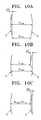
- FIGS. 10A through 10Care schematic views showing deviation of the total pitch of the evaporation mask of FIG. 4 and a line deviation of the evaporation mask;
- FIG. 11is a plan view of part of a mask unit of an evaporation mask according to another embodiment of the present invention.
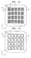
- FIGS. 12 and 13are plan views of evaporation masks according to different embodiments of the present invention.
- FIG. 14is a perspective view of an evaporation mask according to yet another embodiment of the present invention.
- FIG. 15is a plan view of the evaporation mask of FIG. 14;
- FIGS. 16 through 19are plan views of evaporation masks according to different embodiments of the present invention.
- FIGS. 20 through 29are views for illustrating a method of manufacturing an organic electroluminescent (EL) device, according to the present invention.
- FIG. 30is an exploded perspective view of an organic EL device according to an embodiment of the present invention.
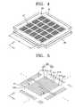
- an evaporation mask 20includes a plurality of mask units 21 . As shown in FIG. 4, the plurality of mask units 21 can be patterned on many products in a single process.
- the evaporation mask 20may be a magnetic thin plate made of nickel or an alloy of nickel and cobalt.
- the evaporation mask 20is made of a nickel-cobalt alloy, which facilitates the formation of fine patterns and provides an excellent surface roughness.
- Apertures 211 and 213 in the evaporation mask 20may be formed in a predetermined pattern by an electro-forming method so as to obtain a fine pattern and an excellent surface smoothness.
- the alloy of Ni and Comay be composed of 85% by weight nickel and 15% by weight cobalt.
- the evaporation mask 20may be manufactured by an etching method, that is, by forming a photoresist layer having a pattern of apertures 211 and 213 on a thin plate, or attaching a film having the pattern of apertures 211 and 213 to a thin plate and then etching the resulting plate.
- tensionis applied to the evaporation mask 20 manufactured by the etching method in x- and y-axis directions while its edges are fixed by a clamp or an adhesive agent. Then, the taut evaporation mask 20 is joined to a mask frame 30 .
- the mask frame 30is hollow so as to support the edge of the evaporation mask 20 excluding the portion where the mask units 21 have been formed.
- the joiningcan be achieved by various methods, such as using an adhesive agent, a laser welding method, or a resistance heating welding method. Especially, the laser welding method can be used to overcome a problem such as an accuracy change or the like.
- reference numeral 31denotes a welding dot used in laser welding.
- a portion of the evaporation mask 20 to be welded to the mask frame 30may be covered by a cover frame to prevent the evaporation mask 20 from coming off the mask frame 30 , in order to overcome stretching or warping of the evaporation mask due to poor welding of the evaporation mask 20 to the mask frame 30 .
- each of the mask units 21 included in the evaporation mask 20includes a pattern of a plurality of apertures 211 and 213 , which are defined by strip-like shielding portions 212 .
- the apertures 211 and 213 shown in FIGS. 4 and 5are elongated in parallel straight lines. However, the apertures 211 and 213 are not limited to such strip shapes, and can be formed in various shapes and patterns, such as lattice or mosaic shapes.
- a rib 22is installed between adjacent mask units 21 so as to keep a distance therebetween.
- the rib 22can be a first rib 221 for isolating mask units 21 arranged in the x-axis direction, or a second rib 222 for isolating mask units 21 arranged in the y-axis direction.
- the apertures 213are first dummy apertures located at the outermost place in a direction in which tension is applied to the evaporation mask 20 , while the apertures 211 are main apertures located inside the first dummy apertures 213 .
- the first dummy apertures 213are used to prevent apertures around the edge of each of the mask units from being deformed by tension applied to the evaporation mask 20 .
- FIG. 5because the main apertures 211 are formed in strips elongated in the y-axis direction, apertures around the edge of each of the mask units 21 may be deformed by the tension applied in the x-axis direction rather than by the tension applied in the y-axis direction.
- the first dummy apertures 213are installed adjacent to some of the main apertures 211 located at the outer side in the x-axis direction.
- the main apertures 211are used to form an effective deposition area that allows a deposition to form a pattern desired by a user, while the first dummy apertures 213 are used to form an ineffective deposition area.
- FIG. 6is a cross-section taken along line II-II of FIG. 5.
- First through third shielding portions 212 a through 212 care sequentially formed in the x-axis direction starting from a first rib 221 to form a mask unit 21 .
- First and second main apertures 211 a and 211 bare sequentially formed in the x-axis direction between the first and second shielding portions 212 a and 212 b and between the second and third shielding portions 212 b and 212 c , respectively.
- a first dummy aperture 213is formed between the first rib 221 and the first shielding portion 212 a.
- the width Wsl of the first main aperture 211 ahas a deviation of ⁇ Ws1
- the width Ws2 of the second main aperture 211 bhas a deviation of ⁇ Ws2.
- ⁇ Wr1denotes a deviation of the width Wr1 of the first shielding portion 212 a
- ⁇ Wsddenotes a deviation of the width Wsd of the first dummy aperture 213 .
- the deviation of the width of each of the main aperturestypically depends on the deviations of the widths of the shielding portions, ⁇ Wr1, ⁇ Wr2, ⁇ Wr3, . . .
- the deviations of the widths of the first dummy aperture 213 and the first and second main apertures 211 a and 211 b , ⁇ Wsd, ⁇ Ws1, and ⁇ Ws2, shown in FIG. 8,are divided by the deviation ⁇ Wr1 of the width of the first shielding portion and then expressed as percentage.
- the deviation ⁇ Wsd of the width of the first dummy aperture 213increases by 25 to 75% of the deviation ⁇ Wr1 of the width of the first shielding portion due to deformation of the edge 221 a of the first rib 221 .
- the deviations of the widths of the first and second main apertures 211 a and 211 b , ⁇ Ws1 and ⁇ Ws2,are nearly the same as the deviation ⁇ Wr1 of the width of the first shielding portion.
- the total pitch Ptis determined as the interval between lines C and D which connect the outermost first main apertures 211 a of two mask units 21 a in the x-axis direction.
- the total pitch Ptmay have a deviation (Pt max ⁇ Pt min).
- a line deviation ( ⁇ X)may be generated.
- the first dummy apertures 213may have the same shape and width as the main apertures 211 , and may be spaced apart from an adjacent first main aperture 211 a by the same interval as the interval between adjacent main apertures 211 .
- the first dummy apertures 213are not limited to the above shape and pattern; any shape and pattern may be adopted as long as the pattern of the main apertures 211 is not affected. For example, as shown in FIG.
- the width Wsd of a first dummy aperture 213may be smaller than the width Ws1 of a first main aperture 211 a
- the width Wr1 of the first shielding portion 212 a between the first dummy aperture 213 and the first main aperture 211 amay be greater than the width Wr2 of the second shielding portion 212 b between the first and second main apertures 211 a and 211 b .
- various shapes and patternsmay be applied.
- first dummy apertures 213are formed near the main apertures located at the outermost edges of each of the mask units 21 .
- the first dummy apertures 213may have a length corresponding to the length of one side of a mask unit 21 and be formed at each side of each mask unit.
- a plurality of first dummy apertures having a length corresponding to the length of one side of each of the lattice-like main apertures 211may be arranged at each side of each mask unit.
- the installation of the first dummy apertures 213 of FIG. 12can also be applied to an evaporation mask 20 of FIG. 13, which includes open mask units 21 that each have a single main aperture 211 .
- an evaporation mask 20according to yet another embodiment of the present invention includes second dummy apertures 22 to improve accuracy.
- FIG. 15is a plan view of the evaporation mask 20 of FIG. 14.
- the evaporation mask 20includes at least two mask units 21 having a predetermined pattern of main apertures 211 . At least one second dummy aperture 22 is formed outside the mask units 21 such as to be adjacent to mask units 21 a and 21 b located at the outermost edges in the direction where tension is applied.
- the main apertures 211 of the evaporation mask 20are strips elongated in the y-axis direction, they are seriously deformed in the x-axis direction, and accordingly, the total pitch Pt is distorted in the x-axis direction.
- the distortion of the total pitch Ptis prevented by forming the second dummy apertures 22 so as to be adjacent to columns of masks 21 a and masks 21 b that are located on the edges of the evaporation mask 20 , particularly, at the outermost sides in the x-axis direction.
- the main apertures 211 formed inside the second dummy apertures 22are prevented from being deformed due to the tension. Consequently, the total pitch Pt is compensated.
- the second dummy apertures 22can be formed in the same shape and with the same width as the main apertures 211 .
- the second dummy apertures 22can have various shapes and patterns as long as they don't affect the pattern of the main apertures 211 .
- the second dummy apertures 22may be formed on the exterior sides of the outermost mask units 21 a and 21 b so as to be as close as possible to the outermost mask units 21 a and 21 b without interfering with deposition areas desired by a user, that is, with effective deposition areas where deposition is achieved through the outermost mask units 21 a and 21 b .
- the second dummy apertures 22must be located inside the welding dots 31 of the evaporation mask 20 .
- alignment marks 23are formed outside a configuration of mask units 21 in order to assist in alignment with a substrate where deposition is to be performed, the alignment marks 23 must not be deformed when tension is applied to the evaporation mask 20 . If the alignment marks 23 are deformed, the evaporation mask 20 is not properly aligned with the substrate, thus causing distortion of the total pitch and inaccurate patterning.
- a pair of second dummy apertures 221 and 222is formed at both sides of each of the alignment marks 23 .
- the inner second dummy aperture 221prevents the total pitch Pt from being distorted, thereby increasing the accuracy of patterning.
- the outer second dummy aperture 222prevents the alignment marks 23 from being deformed, thereby accurately aligning the substrate with the evaporation mask 20 .
- the second dummy apertures 22can be equally applied to the case where the main apertures 211 of each of the mask units 21 are formed in a lattice pattern.
- the main apertures 211have a lattice pattern, a tension in the y-axis direction as well as a tension in the x-axis direction adversely affects the accuracy of the total pitch Pt, so second dummy apertures 22 are also formed adjacent to the main apertures located at the outermost sides in the y-axis direction.
- the way of installing the second dummy apertures 22 as in FIG. 17is also applied to an evaporation mask 20 of FIG. 18 including open mask units 21 , each formed of a single main aperture 211 .
- the total pitchcorresponds to the interval between the outermost main apertures in the outermost mask units.
- the evaporation mask 20 according to the present inventionis not limited to the above determination of the length of the total pitch, but can be formed of a combination of the first dummy apertures 213 and the second dummy apertures 22 as shown in FIG. 19.
- the combination of the first and second dummy apertures 213 and 22respectively, may be a combination of all of the above-described embodiments.
- each of the mask units 21prevents deformation of its main apertures forming an effective deposition area and improves the accuracy of the total pitch. Thus, highly accurate patterning can be achieved.
- a transparent conductive film 43 and a metal conductive film 44are sequentially stacked on a transparent substrate 41 .
- the transparent conductive film 43may be formed of ITO, and the metal conductive film 44 may be formed of chrome (Cr).
- the substrate 41may be formed of transparent glass, plastic, or the like.
- a buffer layer 42may be formed to provide a smooth substrate and prevent penetration of impure atoms.
- the buffer layer 42may be formed of SiO 2 .
- the substrate 41may be large enough to form at least two organic EL devices thereon through a single process.
- FIG. 21refers to the case where a plurality of organic EL devices are manufactured in a single process. However, for convenience of explanation, the manufacture of a single organic EL device will now be described by cutting off an organic EL device from the plurality of EL devices as shown in FIG. 21.
- FIG. 22Arefers to an organic EL device of FIG. 21, and FIG. 22B is a cross-section taken along line III-III of FIG. 22A.
- the external electrode terminals 441 and 442are the basis of the formation of the first and second electrode terminals 51 and 52 of FIG. 23A, and the transparent conductive film 43 is partially exposed on the substrate 41 .
- FIGS. 23A through 23Cinternal electrode terminals 431 and 432 for the first and second electrodes 51 and 52 and a predetermined pattern of transparent conductive lines 433 are formed by patterning the exposed portion of the transparent conductive film 43 on the substrate 41 .
- the transparent conductive lines 433are connected to the first electrode terminals 51 and serve as first electrode lines 61 .
- FIG. 23Bis a cross-section taken along line IV-IV of FIG. 23A
- FIG. 23Cis a cross-section taken along line V-V of FIG. 23A.
- the patterning of the transparent conductive film 43may be achieved by photolithography.
- FIG. 24Bis a cross-section taken along line VI-VI of FIG. 24A.
- the inter-insulator 64may be formed of photoresist, photosensitive polyimide, or the like using a photolithography method or the like.
- a shielding wallmay be further formed inside and outside a place to be coated with an adhesive agent so as to seal up a cap, and an outer-insulator may be formed between the first electrode line 61 and the second electrode terminal 52 .
- the outer-insulatoris formed to prevent problems such as disconnection due to the step difference between second electrode lines and the second electrode terminals 52 upon formation of the second electrode lines.
- a buffer layermay be further formed below the outer-insulator by processing the transparent conductive film 43 to improve the adhesive strength between the outer-insulator and a substrate.
- Separatorsmay be simultaneously formed to form an organic EL film and a pattern of second electrode lines. Partitions for preventing the organic EL film from being damaged may be formed simultaneously. Shielding portions may be formed simultaneously on the place to be coated with an adhesive agent.
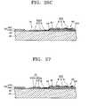
- an organic filmis deposited using an evaporation apparatus shown in FIG. 25.
- an evaporation source 92 for evaporating an organic materialis installed within a chamber 91 in a vacuum state, and the evaporation mask 20 supported by the mask frame 30 is installed over the evaporation source 92 .
- the substrate 41 having first electrode lines and an inter-insulator formed thereonis mounted over the evaporation mask 20 .
- a magnet unit 93is closely installed over the substrate 41 .
- an organic film 63is deposited using an evaporation apparatus as shown in FIG. 25.
- the organic film 63can be any organic film used in an organic EL device, and can be formed by stacking a hole transport layer, an organic luminescent layer, an electron transport layer, and the like to form a single or complex structure.
- the organic film 63can be made of various organic materials including copper phthalocyanine (CuPc), N, N′-Di (naphthalene-1-yl)-N, N′-diphenyl-benzidine (NPB), and tris-8-hydroxyquinoline aluminum (Alq3).
- CuPccopper phthalocyanine
- NNBN′-Di (naphthalene-1-yl)-N
- Alq3tris-8-hydroxyquinoline aluminum
- the organic film 63can be formed in various patterns such that the patterned organic luminescent layer corresponds to the color of each pixel.
- the organic film 63may be formed after the evaporation mask 20 is mounted on the evaporation apparatus of FIG. 25.
- the evaporation mask 20may be the evaporation mask 20 according to any of the embodiments of the present invention described with reference to FIGS. 4 through 19.
- the evaporation mask 20 having the main apertures 211 and the first dummy apertures 213can be used to form an organic film.
- the first dummy apertures 213are formed adjacent to the outermost main apertures 211 a in a direction in which tension is applied, i.e., in a direction perpendicular to the direction of the length of the main apertures 211 .
- the evaporation mask 20 having the second dummy apertures 22included in at least two mask units for forming an organic EL device, can be used to form an organic film.
- the second dummy apertures 22are formed outside the mask units, adjacent to mask units in a direction in which tension is applied, i.e., in a direction perpendicular to the direction of the length of the main apertures 211 .
- an evaporation mask having both the first and second dummy apertures 213 and 22 , respectively,can be used to form an organic film.
- the organic film 63is formed by depositing a hole transport layer 631 on the first electrode lines 61 and the inter-insulators 64 and then depositing red (R), green (G), and blue (B) organic luminescent layers 632 on the hole transport layer 631 such as to form color patterns.
- the hole transport layer 631can be blanket deposited without patterns, and the organic luminescent layers 632 may be formed in a pattern.
- the organic luminescent layers 632 having a patternare deposited using the above-described evaporation masks according to the present invention.
- the R, G, and B organic luminescent layers 632formed on the first electrode lines 61 , correspond to areas where the first electrode lines intersect with the second electrode lines, and accordingly emit light in response to the application of power.
- the R, G, and B organic luminescent layers 632form an effective luminescent area 60 .
- dummy organic luminescent layers 632 aare further deposited between the second electrode terminals 52 and the first electrode lines 61 , that is, the effective luminescent area 60 , through the first dummy apertures.
- the dummy organic luminescent layers 632 aform the first dummy pattern area 70 .
- the first dummy pattern area 70further includes a dummy hole transport layer 631 a .
- organic filmscan be deposited to the same height in the first dummy pattern area 70 by controlling the widths of the first dummy apertures 213 of FIG. 13.
- the first dummy pattern area 70is formed outside the effective luminescent area 60 where the first electrode lines intersect with the second electrode lines, that is, formed in an area where the first electrode lines do not intersect with the second electrode lines, the first dummy pattern area 70 corresponds to an ineffective luminescent area where no light emission occurs.
- the deposition using an evaporation mask capable of forming the first dummy pattern area 70contributes to improvement of the accuracy of patterning in the effective luminescent area 60 .
- the second electrode lines 62may be formed of aluminum (Al) or calcium (Ca) in a predetermined pattern on the organic film 63 such as to intersect with the first electrode lines 61 .
- the second electrode lines 62may be formed using an evaporation mask in an evaporation apparatus as shown in FIG. 25.
- the second electrode lines 62may be patterned using an evaporation mask having a predetermined pattern or by previously installing a separator for forming a pattern and then performing blanket deposition on the separator.
- the second electrode lines 62can be patterned using the evaporation mask having first and/or second dummy apertures described with reference to FIGS. 4 through 19.
- FIG. 29shows an example of patterning the second electrode lines 62 using an evaporation mask.
- second electrode lines 62having a pattern of main apertures 211 and the first dummy apertures 213 , is used to form the second electrode lines 62 , second dummy electrode lines 62 a are deposited on the exterior side of the effective luminescent area 60 , which is where the organic film 63 emits light due to the crossing of the first and second electrode lines 61 and 62 .
- the second dummy electrode lines 62 aform a second dummy pattern area 71 . Because the second dummy electrode lines 62 a are not connected to second electrode terminals which receive external power, the second dummy pattern area 71 corresponds to an ineffective luminescent area where no light emission occurs, as in the first dummy pattern area 70 .
- the second dummy electrode lines 62 amay be formed outside the effective luminescent area 60 on the upper surface of the organic film 63 so as not to contact the first electrode lines 61 .
- a method of depositing an organic film using an evaporation mask forming an organic film and depositing second electrode lines using an evaporation mask forming second electrodesis described above. However, it is natural that the second electrode lines may be deposited using an evaporation mask according to the present invention regardless of which evaporation mask is used to deposit the organic film.
- a sealing cap 81is joined to the substrate 41 so as to serve as a sealing portion 80 .
- a flexible printed circuit board 82is connected to the first and second electrode terminals 51 and 52 exposed to the outside of the sealing portion 80 , thereby completing the assembly of an organic EL device.
- the sealingmay be achieved by any other methods applied to organic EL devices.
- the organic EL device according to the present inventionhas the effective luminescent area 60 where an organic film is formed between the first and second electrode lines 61 and 62 .
- the organic EL device according to the present inventionalso includes a terminal unit 50 having the first and second electrode terminals 51 and 52 , which supply power to the first and second electrode lines 61 and 62 , respectively, of the effective luminescent area 60 .
- the organic EL device according to the present inventionmay include the second dummy pattern area 71 and/or the first dummy pattern area 70 , which is formed outside the effective luminescent area 60 , that is, between the effective luminescent area 60 and the terminal unit 50 . Since the structures and functions of the components of the organic EL device according to the present invention have been described with reference to FIGS. 20 through 29, they will not be described here in detail.
- an organic EL device having first and/or second dummy pattern areas in an ineffective luminescent areais manufactured using an evaporation mask having first and/or second dummy apertures, thereby improving the accuracy of patterning of an effective luminescent area where light emission occurs.
- the present inventionhas the following effects. Firstly, the accuracy of the patterning of an effective deposition area may be improved.
- a substratemay be accurately aligned with an evaporation mask.
- an organic EL deviceincludes a dummy pattern area, that is, an ineffective luminescent area, an effective luminescent area where light emission occurs may have smaller pixels, resulting in a finer resolution.
Landscapes
- Chemical & Material Sciences (AREA)
- Engineering & Computer Science (AREA)
- Manufacturing & Machinery (AREA)
- Chemical Kinetics & Catalysis (AREA)
- Materials Engineering (AREA)
- Mechanical Engineering (AREA)
- Metallurgy (AREA)
- Organic Chemistry (AREA)
- Electroluminescent Light Sources (AREA)
- Physical Vapour Deposition (AREA)
Abstract
Description
- This application claims the benefit of Japanese Application No. 2002-347977, filed Nov. 29, 2002, in the Japanese Intellectual Property Office, the disclosure of which is incorporated herein by reference.[0001]
- 1. Field of the Invention[0002]
- The present invention relates to an evaporation mask, and, more particularly, to an evaporation mask in which the pitch between adjacent apertures can be kept even when a tension is applied, a method of fabricating an organic electroluminescent (EL) device using the evaporation mask, and an organic EL device manufactured using the above method.[0003]
- 2. Description of the Related Art[0004]
- EL devices, which are spontaneous light-emitting display devices, provide a wide viewing angle, good contrast, and a high response speed. Accordingly, much attention is being focused on EL devices because they can be used as a next-generation display device.[0005]
- EL devices are classified as inorganic EL devices or organic EL devices, depending on what material is used to form a light-emitting layer. Organic EL devices have a higher brightness and faster responsivity than inorganic EL devices, and can provide color display, so they are presently being more actively developed.[0006]
- Organic EL devices include first electrodes formed in a predetermined pattern on a transparent insulating substrate, an organic film formed on the first electrodes by vacuum evaporation, and second electrodes formed on the organic film such that the first and second electrodes cross each other.[0007]
- In the manufacture of the organic EL devices having such a structure, the first electrodes are typically formed by patterning indium tin oxide (ITO) using a photolithographic method.[0008]
- Such a photolithographic method can be used before an organic film is formed, but causes a problem when it is used after an organic film is formed. Because the organic film is very sensitive to water, it must be thoroughly isolated from water both while being fabricated and after the fabrication. Consequently, a photolithographic method including an exposure to water during pealing-off and etching of a resist is not suitable for patterning the organic film and the second electrode layer.[0009]
- This problem is usually solved by vacuum-depositing an organic light emissive material for the organic film and a material for the second electrode layer using a patterned mask. In particular, the second electrode layer can be patterned using a cathode separator, but it is known that a vacuum evaporation method using an evaporation mask is the most appropriate way to pattern a low molecular organic film.[0010]
- A technique of patterning an organic film or a second electrode layer using a mask is very important in the manufacture of full-color organic EL devices.[0011]
- Examples of conventional full-color organic EL device coloring methods include a three-color independent evaporation method, in which red (R), green (G), and blue (B) color pixels are independently deposited on a substrate, a color conversion method (CCM), in which a color conversion layer is formed on a light emissive surface using a blue light source, and a color filtering method, which uses a white light source and a color filter. The three-color independent evaporation method has attracted much attention because it is simple to perform, and provides a high color purity and efficiency.[0012]
- In the three-color independent evaporation method, the R, G, and B color pixels are independently deposited on a substrate using an evaporation mask. Here, the evaporation mask must be made of a material with a low thermal expansion coefficient in order to prevent thermal deformation, and also must be magnetic if the evaporation mask is to be adhered to the substrate using a magnet. More importantly, the evaporation mask must be highly accurate. In particular, the positions of deposited pixels, that is, the widths of pattern apertures, must be highly accurate, and a high accuracy of a total mask pitch is also required. For example, if an organic EL device must have a high fineness of 130 ppi or greater and an aperture efficiency of 50% or greater, deviation in the widths of apertures of the evaporation mask must not exceed ±5 μm, and deviation in the total mask pitch must not exceed ±10 μm.[0013]
- As shown in FIG. 1, an[0014]
evaporation mask 10 used to deposit an organic film or electrodes when fabricating an organic EL device is typically supported by aframe 20, so that theevaporation mask 10 is drawn taut. In themask 10, a plurality ofmask units 12, allowing a single organic EL device to be formed thereon, are formed on a single metalthin plate 11. - Because the[0015]
evaporation mask 10 is thinly formed and minutely patterned, if it is used without any treatment, some parts of it may droop, preventing accurate patterning. Accordingly, as shown in FIG. 1, optimal tension in the x- and y-axis directions is applied to theevaporation mask 10 to obtain a predetermined accuracy of a total pitch (Pt), and thetaut evaporation mask 10 is coupled to themask frame 20. Upon coupling, it is important to not change the Pt accuracy. The coupling of theevaporation mask 10 to themask frame 20 can be achieved by various methods such as using an adhesive, laser welding, or resistance welding. - Each of the[0016]
mask units 12 includes a pattern of apertures. As shown in FIG. 1, each of themask units 12 may have strip-like apertures elongated in the y-axis direction. However, the tension makes it difficult for the outermost apertures of each of themask units 12 to maintain a predetermined level of accuracy. - FIG. 2 is a cross-section of a[0017]
mask unit 12 taken along line I-I of FIG. 1, which showsapertures 13 formed in themask unit 12. As shown in FIG. 2, ashielding portion 14 is provided betweenadjacent apertures 13, andoutermost apertures 13aare each defined by ashield portion 14 and arib 15 between adjacent mask units. - As shown in FIG. 2, if tension is applied to the[0018]
evaporation mask 10 having theapertures 13 in the x- and y-axis directions as shown in FIG. 1, anedge portion 15aof therib 15 may curve upward. Such deformation of theedge portion 15aof therib 15 degrades the accuracy of the widths of each of theoutermost apertures 13a. Hence, the accuracy of deposition performed on an organic emissive film through theoutermost apertures 13ais degraded, and, consequently, accurate patterning of the organic emissive film is not accomplished outside a panel. If an edge of a rib between adjacent mask units is deformed, the deformed rib contacts the organic emissive film, thus generating a defect such as a dark point or a pixel short-circuit on the perimeter of a panel. - As shown in FIG. 3, this problem affects the outermost mask units more than other mask units, thus degrading the accuracy of the total mask pitch.[0019]
- In other words, as shown in FIG. 3, particularly,[0020]
mask units apertures 13, that is, in the x-axis direction where tension is applied, may be deformed more seriously thanother mask units 12 due to the tension applied in the x-axis direction. Accordingly, the accuracy of a total pitch (Pt), the gap between aline 16aconnecting the edges of the outer ribs of themask units 12aand aline 16bconnecting the edges of the outer ribs of themask units 12b, decreases, resulting in degradation of the accuracy of patterning of themask units 12. - A mask that overcomes the problem of the deformation of strips that form slits due to thermal expansion of the mask is disclosed in Japanese Patent Publication No. 2001-247961. The disclosed mask includes a mask portion and a screen portion. The mask portion is an evaporation mask used to form a patterning film on a substrate by evaporation, and has partitions for defining a plurality of first apertures. The screen portion contains a magnetic material and has a plurality of second apertures smaller than the first apertures. The second apertures are disposed on the first apertures of the mask portion.[0021]
- Japanese Patent Publication No. 2001-273979 discloses the structure of a magnetic mask. Japanese Patent Publication No. 2001-254169 discloses an evaporation mask frame assembly in which a patterned mask masks a deposition area while adhering closely to a material to be deposited, and has fine gaps and fine patterns. The fine patterns of the patterned mask are supported by fine ribs.[0022]
- These disclosed masks adhere closely to a material to be deposited because they are formed of a magnetic material. However, these masks still have a problem of losing accuracy due to the deformation of the outermost apertures during a tensing operation.[0023]
- Japanese Patent Publication No. 2002-9098 discloses a pattern forming apparatus for preventing a pre-formed film on a substrate from being damaged due to a mask coming partially off of a frame due to a thermal expansion during evaporation. The pattern forming apparatus includes a support which is formed to be larger than the mask, and has a dent portion onto which the mask is seated. The support prevents a mask from becoming rippled due to thermal expansion during the formation of a film. Also, by forming a magnetic element on the side of the mask facing away from the support, the magnetic element makes the mask closer to the substrate so that a space between the mask and the support is created. This space contributes to cooling the mask.[0024]
- However, because the disclosed mask having slits is not firmly supported by the frame, the location of the mask cannot be accurately controlled. In particular, in the case of organic EL devices that must have very thin evaporation masks to accomplish highly accurate patterning, the location of the evaporation mask may be changed during evaporation.[0025]
- Japanese Patent Publication No. 2002-8859 discloses a pattern forming apparatus for preventing a mask from being expanded by heat during the formation of a film, in which a liquid path is formed within a frame which supports the mask, and a cooling solution circulates within the liquid path. However, this invention also overlooks the possibility of tensions and apertures becoming inaccurate during fixation of the mask into the frame.[0026]
- Japanese Patent Publication Nos. 2000-48954, 2000-173769, 2001-203079, and 2001-110567 disclose metal masks including supplementary lines to prevent drooping of a mask shield between the mask and a frame. Like the above-disclosed masks, these masks may be stretched and warped while being fixed onto a frame after applying tension in order to accomplish highly accurate patterning.[0027]
- The present invention provides an evaporation mask that reduces deviation of patterns by reducing variation in the accuracy of the widths of apertures that may be caused by supporting a taut evaporation mask, a method of manufacturing an organic EL device using the evaporation mask, and an organic EL device manufactured by the method.[0028]
- The present invention also provides an evaporation mask that improves pattern accuracy by compensating for a total pitch when tension is applied to the evaporation mask, a method of manufacturing an organic EL device using the evaporation mask, and an organic EL device manufactured by the method.[0029]
- Additional aspects and/or advantages of the invention will be set forth in part in the description which follows and, in part, will be obvious from the description, or may be learned by practice of the invention.[0030]
- According to an aspect of the present invention, there is provided an evaporation mask formed of a thin film, wherein the evaporation mask is drawn taut by application of tension and comprises at least one mask unit. The mask unit includes a plurality of main apertures and a plurality of first dummy apertures formed adjacent to outermost ones of the main apertures in a direction in which tension is applied to the evaporation mask.[0031]
- The main apertures may form an effective deposition area, and the first dummy apertures may form an ineffective deposition area.[0032]
- At least one of the first dummy apertures may be formed parallel to the main apertures, and at least another one of the first dummy apertures may be formed perpendicular to the main apertures.[0033]
- The evaporation mask may comprise at least two mask units, and may further comprise a plurality of second dummy apertures formed outside and adjacent to the outermost mask units in the direction in which tension is applied to the evaporation mask.[0034]
- The second dummy apertures may be formed outside the effective deposition areas where the mask units are formed.[0035]
- Alternatively, at least one of the second dummy apertures may be formed parallel to the main apertures of the mask units, and at least another one of the second dummy apertures may be formed perpendicular to the main apertures.[0036]
- According to an aspect of the present invention, there is provided another evaporation mask formed of a thin film, wherein the evaporation mask is drawn taut by application of tension. The evaporation mask includes at least two mask units each having at least one main aperture and at least one second dummy aperture formed outside and adjacent to the mask units located at the outermost sides in the direction in which tension is applied to the evaporation mask.[0037]
- The at least one main aperture of each of the mask units may be used to form an effective deposition area, and the at least one second dummy aperture may be formed outside of the effective deposition areas where the mask units are formed.[0038]
- Alternatively, the at least one second dummy aperture may comprise at least two second dummy apertures, wherein at least one of the second dummy apertures may be formed parallel to the at least one main aperture of the mask units, and at least another one of the second dummy apertures may be formed perpendicular to the at least one main aperture.[0039]
- According to another aspect of the present invention, there is provided a method of manufacturing an organic electroluminescent (EL) device. In this method, first electrodes are formed on a substrate. Next, an evaporation mask to form an organic film is disposed over the substrate. Here, the evaporation mask is drawn taut by application of tension and has at least one mask unit. The mask unit comprises a plurality of main apertures and a plurality of first dummy apertures formed adjacent to outmost main apertures in a direction in which tension is applied to the evaporation mask. The organic film comprises an effective luminescent area formed to cover at least the first electrodes by evaporating an organic material containing an organic luminescent material through the main apertures. At this time, a first dummy pattern area is formed outside the effective luminescent area through the first dummy apertures. Thereafter, second electrodes are formed on the organic film so that the effective luminescent area is formed at an area where the first and second electrodes overlap. Finally, the resulting structure is sealed.[0040]
- At least one of the first dummy apertures may be formed parallel to the main apertures, and at least another one of the first dummy apertures may be formed perpendicular to the main apertures.[0041]
- At least two organic EL devices may be manufactured in a single process, and the evaporation mask may comprise at least two mask units, through each of which the organic film of a single organic EL device can be deposited, and a plurality of second dummy apertures outside and adjacent to outermost ones of the mask units in the direction in which tension is applied to the evaporation mask.[0042]
- The second dummy apertures of the evaporation mask may be located outside the effective luminescent areas of the organic EL devices that may be deposited by the outermost mask units adjacent to the second dummy apertures.[0043]
- At least one of the second dummy apertures may be formed parallel to the main apertures of the mask units, and at least one of the second dummy apertures may be formed perpendicular to the main apertures.[0044]
- To form the second electrodes, first, an evaporation mask to form the second electrodes may be disposed over the substrate. Here, the evaporation mask is drawn taut by application of tension and has at least one mask unit. The mask unit comprises a plurality of main apertures and a plurality of first dummy apertures formed adjacent to the outermost main apertures in the direction in which tension is applied to the evaporation mask. Then, the second electrodes may be formed on the effective luminescent area through the main apertures, and a second dummy pattern area may be formed outside the effective luminescent area through the first dummy apertures.[0045]
- At least one of the first dummy apertures may be formed parallel to the main apertures, and at least another one of the first dummy apertures may be formed perpendicular to the main apertures.[0046]
- At least two organic EL devices may be manufactured in a single process. The evaporation mask may comprise at least two mask units, through each of which the second electrodes of a single organic EL device can be deposited, and a plurality of second dummy apertures outside and adjacent to the outermost mask units in the direction in which tension is applied to the evaporation mask.[0047]
- The second dummy apertures may be located outside the effective luminescent areas of the organic EL devices that are deposited by the outermost mask units adjacent to the second dummy apertures.[0048]
- At least one of the second dummy apertures may be formed parallel to the main apertures of the mask units, and at least another one of the second dummy apertures may be formed perpendicular to the main apertures.[0049]
- At least two organic EL devices may be manufactured in a single process. The second electrodes may be formed using an evaporation mask drawn taut by application of tension and having at least two mask units, through which the second electrodes of the organic EL device can be deposited. The evaporation mask may comprise a plurality of second dummy aperture outside and adjacent to outermost mask units in the direction in which tension is applied to the evaporation mask.[0050]
- The second dummy apertures may be located outside the effective luminescent areas of the organic EL devices that are deposited by the outermost mask units adjacent to the second dummy apertures.[0051]
- At least one of the second dummy apertures may be formed parallel to the main apertures of the mask units, and at least another one of the second dummy apertures may be formed perpendicular to the main apertures.[0052]
- According to another aspect of the present invention, there is provided another method of manufacturing an organic EL device. In this method, first electrodes for an organic EL device are formed on a substrate. Next, an evaporation mask to form an organic film is disposed over the substrate. Here, the evaporation mask is drawn taut by application of tension and includes at least two mask units. Each of the mask units comprises a plurality of main apertures and a plurality of second dummy apertures formed outside and adjacent to outermost ones of the mask units in a direction in which tension is applied to the evaporation mask. The organic film comprising an effective luminescent area is formed to cover at least the first electrodes by evaporating an organic material containing an organic luminescent material through the main apertures of each of the mask units. Thereafter, second electrodes are formed on the organic film so that the effective luminescent area is formed at an area where the first and second electrodes overlap. Finally, the resulting structure is sealed.[0053]
- The second dummy apertures may be located outside the effective luminescent areas of the organic EL devices that are deposited by outermost ones of the mask units adjacent to the second dummy apertures.[0054]
- Alternatively, the second dummy apertures may be formed parallel to the main apertures of the mask units, and at least another one of the second dummy apertures may be formed perpendicular to the main apertures.[0055]
- In an alternative process of forming the second electrodes, an evaporation mask to form the second electrodes may be disposed over the substrate. Here, the evaporation mask may be drawn taut by application of tension and includes at least two mask units. Each of the mask units may comprise a plurality of main apertures and a plurality of first dummy apertures formed adjacent to the outermost main apertures in the direction in which tension is applied to the evaporation mask. Then, the second electrodes may be formed on each of the effective luminescent areas through the main apertures, and a second dummy pattern area may be formed outside each of the effective luminescent areas through the first dummy apertures.[0056]
- At least one of the first dummy apertures may be formed parallel to the main apertures, and at least another one of the first dummy apertures may be formed perpendicular to the main apertures.[0057]
- The evaporation mask may comprise a plurality of second dummy apertures outside and adjacent to the outermost mask units in the direction in which tension is applied to the evaporation mask.[0058]
- The second dummy apertures of the evaporation mask may be located outside the effective luminescent areas of the organic EL devices that are deposited by the outermost mask units adjacent to the second dummy apertures.[0059]
- At least one of the second dummy apertures may be formed parallel to the main apertures of the mask units, and at least another one of the second dummy apertures may be formed perpendicular to the main apertures.[0060]
- In another alternative process of forming the second electrodes, the second electrodes may be formed using an evaporation mask. The evaporation mask may be drawn taut by application of tension and may have at least two mask units, through each of which the second electrodes of the organic EL devices may be deposited. The evaporation mask may comprise a plurality of second dummy apertures outside and adjacent to outermost mask units in the direction in which tension is applied to the evaporation mask.[0061]
- At least one of the second dummy apertures of the evaporation mask may be located outside the effective luminescent areas of the organic EL device that may be deposited by the outermost mask units adjacent to the second dummy apertures.[0062]
- The second dummy apertures may be formed parallel to the main apertures of the mask units, and at least one of the second dummy apertures may be formed perpendicular to the main apertures.[0063]
- According to another aspect of the present invention, there is provided still another method of manufacturing an organic EL device. In this method, first electrodes are formed on a substrate in a predetermined pattern. Next, an organic film comprising an effective luminescent area is formed to cover at least the first electrodes by evaporating an organic material containing an organic luminescent material. Thereafter, an evaporation mask to form second electrodes is disposed over the organic film. Here, the evaporation mask is drawn taut by application of tension and comprises a plurality of main apertures and a plurality of dummy apertures formed adjacent to the outermost ones of the main apertures in a direction in which tension is applied to the evaporation mask. Second electrodes are formed through the main apertures so that the effective luminescent area is formed at an area where the first and second electrodes overlap. At this time, a second dummy pattern area is formed outside the effective luminescent area through the first dummy apertures. Finally, the resulting structure is sealed.[0064]
- At least one of the first dummy apertures may be formed parallel to the main apertures, and at least another one of the first dummy apertures may be formed perpendicular to the main apertures.[0065]
- At least two organic EL devices may be manufactured in a single process. The evaporation mask may comprise at least two mask units, through each of which the second electrodes of a single organic EL device can be deposited, and a plurality of second dummy apertures outside and adjacent to outermost ones of the mask units in the direction in which tension is applied to the evaporation mask.[0066]
- The second dummy apertures of the evaporation mask may be located outside the effective luminescent areas of the organic EL devices that may be deposited by the outermost mask units adjacent to the second dummy apertures.[0067]
- At least one of the second dummy apertures may be formed parallel to the main apertures of the mask units, and at least another one of the second dummy apertures may be formed perpendicular to the main apertures.[0068]
- According to another aspect of the present invention, there is provided still yet another method of manufacturing an organic EL device. In this method, first electrodes for an organic EL device are formed on a substrate. Next, an organic film comprising an effective luminescent area is formed to cover at least the first electrodes by evaporating an organic material containing an organic luminescent material. An evaporation mask to form second electrodes is disposed over the organic film. Here, the evaporation mask is drawn taut by application of tension and comprises at least two mask units. Each of the mask units comprises a plurality of main apertures and a plurality of second dummy apertures formed outside and adjacent to the outermost ones of the mask units in a direction in which tension is applied to the evaporation mask. Second electrodes are formed through the main apertures of each of the mask units so that the effective luminescent area is formed at an area where the first and second electrodes overlap. Finally, the resulting structure is sealed.[0069]
- The second dummy apertures of the evaporation mask may be located outside the effective luminescent areas of the organic EL devices that may be deposited by the outermost mask units adjacent to the second dummy apertures.[0070]
- At least one of the second dummy apertures may be formed parallel to the main apertures of the mask units, and at least one of the second dummy apertures may be formed perpendicular to the main apertures.[0071]
- According to still another aspect of the present invention, there is provided an organic EL device including a substrate, an effective luminescent area, a terminal unit, a sealing unit, and a dummy pattern area. The effective luminescent area is formed by sequentially stacking first electrodes, an organic film including an organic luminescent layer, and second electrodes on the substrate. The organic film emits light at the area where the first and second electrodes overlap. The terminal unit is formed on the edge of the substrate outside the effective luminescent area and has a first electrode terminal connected to the first electrodes and a second electrode terminal connected to the second electrodes. The sealing unit is formed on the substrate so as to expose the terminal unit and seal at least the effective luminescent area. The dummy pattern area is formed outside of the effective luminescent area.[0072]
- The dummy pattern area may be formed between the effective luminescent area and the terminal unit.[0073]
- The dummy pattern area may be formed inside an area sealed by the sealing unit.[0074]
- The dummy pattern area may be formed of the same material as the organic luminescent layer.[0075]
- The dummy pattern area may be formed of the same material as the organic film.[0076]
- The dummy pattern area may be formed of the same material as the second electrodes.[0077]
- The dummy pattern area may be formed on the outside of the organic luminescent area in an upper area of the organic film.[0078]
- These and/or other aspects and advantages of the invention will become apparent and more readily appreciated from the following description of the embodiments, taken in conjunction with the accompanying drawings of which:[0079]
- FIG. 1 is an exploded perspective view of a conventional evaporation mask;[0080]
- FIG. 2 is a cross-section of part of the evaporation mask of FIG. 1;[0081]
- FIG. 3 is a plan view of the evaporation mask of FIG. 1;[0082]
- FIG. 4 is a perspective view of an evaporation mask according to an embodiment of the present invention;[0083]
- FIG. 5 is a partial perspective view of a mask unit of the evaporation mask of FIG. 4;[0084]
- FIGS. 6 and 7 are cross-sections taken along line II-II of FIG. 5;[0085]
- FIG. 8 is a graph showing deviation in the widths of apertures in a mask according to the present invention;[0086]
- FIG. 9 is a plan view of the evaporation mask of FIG. 4;[0087]
- FIGS. 10A through 10C are schematic views showing deviation of the total pitch of the evaporation mask of FIG. 4 and a line deviation of the evaporation mask;[0088]
- FIG. 11 is a plan view of part of a mask unit of an evaporation mask according to another embodiment of the present invention;[0089]
- FIGS. 12 and 13 are plan views of evaporation masks according to different embodiments of the present invention;[0090]
- FIG. 14 is a perspective view of an evaporation mask according to yet another embodiment of the present invention;[0091]
- FIG. 15 is a plan view of the evaporation mask of FIG. 14;[0092]
- FIGS. 16 through 19 are plan views of evaporation masks according to different embodiments of the present invention;[0093]
- FIGS. 20 through 29 are views for illustrating a method of manufacturing an organic electroluminescent (EL) device, according to the present invention; and[0094]
- FIG. 30 is an exploded perspective view of an organic EL device according to an embodiment of the present invention.[0095]
- Reference will now be made in detail to the embodiments of the present invention, examples of which are illustrated in the accompanying drawings, wherein like reference numerals refer to the like elements throughout. The embodiments are described below to explain the present invention by referring to the figures.[0096]
- Referring to FIGS. 4 through 6, an[0097]
evaporation mask 20 according to an embodiment of the present invention includes a plurality ofmask units 21. As shown in FIG. 4, the plurality ofmask units 21 can be patterned on many products in a single process. Theevaporation mask 20 may be a magnetic thin plate made of nickel or an alloy of nickel and cobalt. Preferably, theevaporation mask 20 is made of a nickel-cobalt alloy, which facilitates the formation of fine patterns and provides an excellent surface roughness.Apertures evaporation mask 20 may be formed in a predetermined pattern by an electro-forming method so as to obtain a fine pattern and an excellent surface smoothness. The alloy of Ni and Co may be composed of 85% by weight nickel and 15% by weight cobalt. - The[0098]
evaporation mask 20 may be manufactured by an etching method, that is, by forming a photoresist layer having a pattern ofapertures apertures - As shown in FIG. 4, tension is applied to the[0099]
evaporation mask 20 manufactured by the etching method in x- and y-axis directions while its edges are fixed by a clamp or an adhesive agent. Then, thetaut evaporation mask 20 is joined to amask frame 30. Themask frame 30 is hollow so as to support the edge of theevaporation mask 20 excluding the portion where themask units 21 have been formed. The joining can be achieved by various methods, such as using an adhesive agent, a laser welding method, or a resistance heating welding method. Especially, the laser welding method can be used to overcome a problem such as an accuracy change or the like. In FIG. 4,reference numeral 31 denotes a welding dot used in laser welding. - Although not shown in the drawings, a portion of the[0100]
evaporation mask 20 to be welded to themask frame 30 may be covered by a cover frame to prevent theevaporation mask 20 from coming off themask frame 30, in order to overcome stretching or warping of the evaporation mask due to poor welding of theevaporation mask 20 to themask frame 30. - As shown in FIG. 5, each of the[0101]
mask units 21 included in theevaporation mask 20 includes a pattern of a plurality ofapertures like shielding portions 212. Theapertures apertures rib 22 is installed betweenadjacent mask units 21 so as to keep a distance therebetween. Therib 22 can be afirst rib 221 for isolatingmask units 21 arranged in the x-axis direction, or asecond rib 222 for isolatingmask units 21 arranged in the y-axis direction. - The[0102]
apertures 213 are first dummy apertures located at the outermost place in a direction in which tension is applied to theevaporation mask 20, while theapertures 211 are main apertures located inside thefirst dummy apertures 213. Thefirst dummy apertures 213 are used to prevent apertures around the edge of each of the mask units from being deformed by tension applied to theevaporation mask 20. As shown in FIG. 5, because themain apertures 211 are formed in strips elongated in the y-axis direction, apertures around the edge of each of themask units 21 may be deformed by the tension applied in the x-axis direction rather than by the tension applied in the y-axis direction. Accordingly, thefirst dummy apertures 213 are installed adjacent to some of themain apertures 211 located at the outer side in the x-axis direction. Here, themain apertures 211 are used to form an effective deposition area that allows a deposition to form a pattern desired by a user, while thefirst dummy apertures 213 are used to form an ineffective deposition area. - FIG. 6 is a cross-section taken along line II-II of FIG. 5. First through[0103]
third shielding portions 212athrough212care sequentially formed in the x-axis direction starting from afirst rib 221 to form amask unit 21. First and secondmain apertures second shielding portions third shielding portions first dummy aperture 213 is formed between thefirst rib 221 and thefirst shielding portion 212a. - In FIG. 6, the width Wsl of the first[0104]
main aperture 211ahas a deviation of ΔWs1, and the width Ws2 of the secondmain aperture 211bhas a deviation of ΔWs2. ΔWr1 denotes a deviation of the width Wr1 of thefirst shielding portion 212a, and ΔWsd denotes a deviation of the width Wsd of thefirst dummy aperture 213. - As shown in FIG. 7, when tension is applied to the evaporation mask having the apertures with the above widths, an[0105]
edge 221aof thefirst rib 221 that defines thefirst dummy aperture 213 located at the edge area of themask unit 21 is lifted upward or downward due to the extension of the evaporation mask in the x-axis direction shown in FIGS. 4 and 5. Hence, the deviation ΔWsd of the width Wsd of thefirst dummy aperture 213 increases. The deviation of the apertures of the evaporation mask after application of tension is shown in FIG. 8. In FIG. 8, reference character A refers to an evaporation mask manufactured by electroforming, and reference character B refers to an evaporation mask manufactured by etching. Since the deviation of the width of each of the main apertures typically depends on the deviations of the widths of the shielding portions, ΔWr1, ΔWr2, ΔWr3, . . . , the deviations of the widths of thefirst dummy aperture 213 and the first and secondmain apertures - As shown in FIG. 8, after tension is applied to the evaporation mask, the deviation ΔWsd of the width of the[0106]
first dummy aperture 213 increases by 25 to 75% of the deviation ΔWr1 of the width of the first shielding portion due to deformation of theedge 221aof thefirst rib 221. The deviations of the widths of the first and secondmain apertures - According to the experiment of FIG. 8, because the[0107]
first dummy aperture 213 is deformed when tension is applied in the x-axis direction, deformation of themain apertures 211 forming an effective deposition area is minimized, and accordingly, highly accurate patterning can be achieved. - As shown in FIG. 9, because the[0108]
first dummy apertures 213 exist at the outermost edges of each of themask units 21, the total pitch Pt is determined as the interval between lines C and D which connect the outermost firstmain apertures 211aof twomask units 21ain the x-axis direction. As shown in FIGS. 10A and 10B, the total pitch Pt may have a deviation (Pt max−Pt min). As shown in FIGS. 10A through 10C, a line deviation (ΔX) may be generated. Hence, theevaporation mask 20 and themask frame 30 must be welded together while controlling tension for local areas so as to reduce both deviation of the total pitch and line deviation. - As shown in FIG. 5, the[0109]
first dummy apertures 213 may have the same shape and width as themain apertures 211, and may be spaced apart from an adjacent firstmain aperture 211aby the same interval as the interval between adjacentmain apertures 211. However, thefirst dummy apertures 213 are not limited to the above shape and pattern; any shape and pattern may be adopted as long as the pattern of themain apertures 211 is not affected. For example, as shown in FIG. 11, the width Wsd of afirst dummy aperture 213 may be smaller than the width Ws1 of a firstmain aperture 211a, and the width Wr1 of thefirst shielding portion 212abetween thefirst dummy aperture 213 and the firstmain aperture 211amay be greater than the width Wr2 of thesecond shielding portion 212bbetween the first and secondmain apertures - The above-described way of shaping and installing[0110]
first dummy apertures 213 is equally applied to the case of FIG. 12, where themain apertures 211 of each of themask units 21 are arranged in a lattice pattern. However, the lattice shape of themain apertures 211 causes both tension in the x- and y-axis directions to affect the accuracy of patterning. Hence, thefirst dummy apertures 213 are formed near the main apertures located at the outermost edges of each of themask units 21. As shown in FIG. 12, thefirst dummy apertures 213 may have a length corresponding to the length of one side of amask unit 21 and be formed at each side of each mask unit. Alternatively, although not shown in the drawings, a plurality of first dummy apertures having a length corresponding to the length of one side of each of the lattice-likemain apertures 211 may be arranged at each side of each mask unit. - The installation of the[0111]
first dummy apertures 213 of FIG. 12 can also be applied to anevaporation mask 20 of FIG. 13, which includesopen mask units 21 that each have a singlemain aperture 211. - As shown in FIG. 14, an[0112]
evaporation mask 20 according to yet another embodiment of the present invention includessecond dummy apertures 22 to improve accuracy. FIG. 15 is a plan view of theevaporation mask 20 of FIG. 14. - As shown in FIGS. 14 and 15, the[0113]
evaporation mask 20 includes at least twomask units 21 having a predetermined pattern ofmain apertures 211. At least onesecond dummy aperture 22 is formed outside themask units 21 such as to be adjacent to maskunits - As shown in FIG. 14, if the[0114]
main apertures 211 of theevaporation mask 20 are strips elongated in the y-axis direction, they are seriously deformed in the x-axis direction, and accordingly, the total pitch Pt is distorted in the x-axis direction. The distortion of the total pitch Pt is prevented by forming thesecond dummy apertures 22 so as to be adjacent to columns ofmasks 21aand masks21bthat are located on the edges of theevaporation mask 20, particularly, at the outermost sides in the x-axis direction. Here, because thesecond dummy apertures 22 are deformed due to tension applied in the x-axis direction, themain apertures 211 formed inside thesecond dummy apertures 22 are prevented from being deformed due to the tension. Consequently, the total pitch Pt is compensated. - As shown in FIGS. 14 and 15, the[0115]
second dummy apertures 22 can be formed in the same shape and with the same width as themain apertures 211. However, thesecond dummy apertures 22 can have various shapes and patterns as long as they don't affect the pattern of themain apertures 211. Also, thesecond dummy apertures 22 may be formed on the exterior sides of theoutermost mask units outermost mask units outermost mask units second dummy apertures 22 must be located inside thewelding dots 31 of theevaporation mask 20. - On the other hand, as shown in FIG. 16, if alignment marks[0116]23 are formed outside a configuration of
mask units 21 in order to assist in alignment with a substrate where deposition is to be performed, the alignment marks23 must not be deformed when tension is applied to theevaporation mask 20. If the alignment marks23 are deformed, theevaporation mask 20 is not properly aligned with the substrate, thus causing distortion of the total pitch and inaccurate patterning. - To avoid deformation of the alignment marks[0117]23, a pair of
second dummy apertures second dummy aperture 221 prevents the total pitch Pt from being distorted, thereby increasing the accuracy of patterning. The outersecond dummy aperture 222 prevents the alignment marks23 from being deformed, thereby accurately aligning the substrate with theevaporation mask 20. - As shown in FIG. 17, the[0118]
second dummy apertures 22 can be equally applied to the case where themain apertures 211 of each of themask units 21 are formed in a lattice pattern. However, because themain apertures 211 have a lattice pattern, a tension in the y-axis direction as well as a tension in the x-axis direction adversely affects the accuracy of the total pitch Pt, sosecond dummy apertures 22 are also formed adjacent to the main apertures located at the outermost sides in the y-axis direction. The way of installing thesecond dummy apertures 22 as in FIG. 17 is also applied to anevaporation mask 20 of FIG. 18 includingopen mask units 21, each formed of a singlemain aperture 211. - Since the[0119]
evaporation mask 20 having thesecond dummy apertures 22 described with reference to FIGS. 14 through 18 does not include thefirst dummy apertures 213, the total pitch corresponds to the interval between the outermost main apertures in the outermost mask units. However, theevaporation mask 20 according to the present invention is not limited to the above determination of the length of the total pitch, but can be formed of a combination of thefirst dummy apertures 213 and thesecond dummy apertures 22 as shown in FIG. 19. Here, the combination of the first andsecond dummy apertures - In the[0120]
evaporation mask 20 of FIG. 19, having the first andsecond dummy apertures mask units 21 prevents deformation of its main apertures forming an effective deposition area and improves the accuracy of the total pitch. Thus, highly accurate patterning can be achieved. - A method of manufacturing an organic EL device using the above-described[0121]
evaporation mask 20 according to the present invention will now be described with reference to FIGS. 20 through 30. Referring to FIG. 20, first, a transparentconductive film 43 and a metalconductive film 44 are sequentially stacked on atransparent substrate 41. The transparentconductive film 43 may be formed of ITO, and the metalconductive film 44 may be formed of chrome (Cr). Thesubstrate 41 may be formed of transparent glass, plastic, or the like. Before the transparentconductive film 43 and the metalconductive film 44 are formed on thesubstrate 41, abuffer layer 42 may be formed to provide a smooth substrate and prevent penetration of impure atoms. Thebuffer layer 42 may be formed of SiO2. Thesubstrate 41 may be large enough to form at least two organic EL devices thereon through a single process. - Next, as shown in FIG. 21,[0122]
external electrode terminals conductive film 44 formed on the upper surface of thesubstrate 41. FIG. 21 refers to the case where a plurality of organic EL devices are manufactured in a single process. However, for convenience of explanation, the manufacture of a single organic EL device will now be described by cutting off an organic EL device from the plurality of EL devices as shown in FIG. 21. - FIG. 22A refers to an organic EL device of FIG. 21, and FIG. 22B is a cross-section taken along line III-III of FIG. 22A. As shown in FIGS. 22A and 22B, the[0123]
external electrode terminals second electrode terminals conductive film 43 is partially exposed on thesubstrate 41. - Thereafter, as shown in FIGS. 23A through 23C,[0124]
internal electrode terminals second electrodes conductive lines 433 are formed by patterning the exposed portion of the transparentconductive film 43 on thesubstrate 41. The transparentconductive lines 433 are connected to thefirst electrode terminals 51 and serve as first electrode lines61. FIG. 23B is a cross-section taken along line IV-IV of FIG. 23A, and FIG. 23C is a cross-section taken along line V-V of FIG. 23A. The patterning of the transparentconductive film 43 may be achieved by photolithography. - Next, as shown in FIGS. 24A and 24B, an inter-insulator[0125]64 is formed between adjacent first electrode lines61. FIG. 24B is a cross-section taken along line VI-VI of FIG. 24A. The inter-insulator64 may be formed of photoresist, photosensitive polyimide, or the like using a photolithography method or the like.
- Although not shown in the drawings, at the same time the inter-insulator[0126]64 is formed, a shielding wall may be further formed inside and outside a place to be coated with an adhesive agent so as to seal up a cap, and an outer-insulator may be formed between the
first electrode line 61 and thesecond electrode terminal 52. As described later, the outer-insulator is formed to prevent problems such as disconnection due to the step difference between second electrode lines and thesecond electrode terminals 52 upon formation of the second electrode lines. A buffer layer may be further formed below the outer-insulator by processing the transparentconductive film 43 to improve the adhesive strength between the outer-insulator and a substrate. Separators may be simultaneously formed to form an organic EL film and a pattern of second electrode lines. Partitions for preventing the organic EL film from being damaged may be formed simultaneously. Shielding portions may be formed simultaneously on the place to be coated with an adhesive agent. - Then, an organic film is deposited using an evaporation apparatus shown in FIG. 25. In the evaporation apparatus of FIG. 25, an[0127]
evaporation source 92 for evaporating an organic material is installed within achamber 91 in a vacuum state, and theevaporation mask 20 supported by themask frame 30 is installed over theevaporation source 92. As described above, thesubstrate 41 having first electrode lines and an inter-insulator formed thereon is mounted over theevaporation mask 20. Amagnet unit 93 is closely installed over thesubstrate 41. - As shown in FIGS. 26A through 26C, an[0128]
organic film 63 is deposited using an evaporation apparatus as shown in FIG. 25. Theorganic film 63 can be any organic film used in an organic EL device, and can be formed by stacking a hole transport layer, an organic luminescent layer, an electron transport layer, and the like to form a single or complex structure. Theorganic film 63 can be made of various organic materials including copper phthalocyanine (CuPc), N, N′-Di (naphthalene-1-yl)-N, N′-diphenyl-benzidine (NPB), and tris-8-hydroxyquinoline aluminum (Alq3). In the case of full color organic EL devices, theorganic film 63 can be formed in various patterns such that the patterned organic luminescent layer corresponds to the color of each pixel. - The[0129]
organic film 63 may be formed after theevaporation mask 20 is mounted on the evaporation apparatus of FIG. 25. Here, theevaporation mask 20 may be theevaporation mask 20 according to any of the embodiments of the present invention described with reference to FIGS. 4 through 19. - In other words, as described above with reference to FIGS. 4 through 13, the[0130]
evaporation mask 20 having themain apertures 211 and thefirst dummy apertures 213 can be used to form an organic film. Here, thefirst dummy apertures 213 are formed adjacent to the outermostmain apertures 211ain a direction in which tension is applied, i.e., in a direction perpendicular to the direction of the length of themain apertures 211. Also, as described above with reference to FIGS. 14 through 19, theevaporation mask 20 having thesecond dummy apertures 22, included in at least two mask units for forming an organic EL device, can be used to form an organic film. Here, thesecond dummy apertures 22 are formed outside the mask units, adjacent to mask units in a direction in which tension is applied, i.e., in a direction perpendicular to the direction of the length of themain apertures 211. Furthermore, although not shown in the drawings, an evaporation mask having both the first andsecond dummy apertures - As shown in FIG. 26C, a first[0131]
dummy pattern area 70 is formed by thefirst dummy apertures 213. FIG. 26C is a partially magnified cross-section of the portion indicated by reference character VIII. - As shown in FIGS. 26A through 26C, the[0132]
organic film 63 is formed by depositing ahole transport layer 631 on thefirst electrode lines 61 and the inter-insulators64 and then depositing red (R), green (G), and blue (B) organicluminescent layers 632 on thehole transport layer 631 such as to form color patterns. Here, thehole transport layer 631 can be blanket deposited without patterns, and the organicluminescent layers 632 may be formed in a pattern. In FIG. 26C, the organicluminescent layers 632 having a pattern are deposited using the above-described evaporation masks according to the present invention. As described above, the R, G, and B organicluminescent layers 632, formed on thefirst electrode lines 61, correspond to areas where the first electrode lines intersect with the second electrode lines, and accordingly emit light in response to the application of power. Thus, the R, G, and B organicluminescent layers 632 form an effectiveluminescent area 60. - As shown in FIG. 26C, if the R, G, and B organic[0133]
luminescent layers 632 are deposited using the evaporation mask having the first dummy apertures, dummy organicluminescent layers 632aare further deposited between thesecond electrode terminals 52 and thefirst electrode lines 61, that is, the effectiveluminescent area 60, through the first dummy apertures. The dummy organicluminescent layers 632aform the firstdummy pattern area 70. - As shown in FIG. 27, if the[0134]
hole transport layer 631 is deposited using an evaporation mask for forming an organic film as shown in FIG. 13, the firstdummy pattern area 70 further includes a dummyhole transport layer 631a. Here, although not shown in the drawings, organic films can be deposited to the same height in the firstdummy pattern area 70 by controlling the widths of thefirst dummy apertures 213 of FIG. 13. - As described above, if evaporation masks capable of forming the first[0135]
dummy pattern area 70 have second dummy apertures, the variation of the total pitch is reduced to thus improve the accuracy of patterning of the effective luminescent area, particularly the organic luminescent layers. - Since the first[0136]
dummy pattern area 70 is formed outside the effectiveluminescent area 60 where the first electrode lines intersect with the second electrode lines, that is, formed in an area where the first electrode lines do not intersect with the second electrode lines, the firstdummy pattern area 70 corresponds to an ineffective luminescent area where no light emission occurs. The deposition using an evaporation mask capable of forming the firstdummy pattern area 70 contributes to improvement of the accuracy of patterning in the effectiveluminescent area 60. - As shown in FIGS. 28A and 28B, after the[0137]
organic film 63 is deposited, thesecond electrode lines 62 may be formed of aluminum (Al) or calcium (Ca) in a predetermined pattern on theorganic film 63 such as to intersect with the first electrode lines61. Like the deposition of theorganic film 63, thesecond electrode lines 62 may be formed using an evaporation mask in an evaporation apparatus as shown in FIG. 25. At this time, thesecond electrode lines 62 may be patterned using an evaporation mask having a predetermined pattern or by previously installing a separator for forming a pattern and then performing blanket deposition on the separator. - For example, as in the deposition of the[0138]
organic film 63 having the organicluminescent layers 632, thesecond electrode lines 62 can be patterned using the evaporation mask having first and/or second dummy apertures described with reference to FIGS. 4 through 19. FIG. 29 shows an example of patterning thesecond electrode lines 62 using an evaporation mask. To be more specific, when theevaporation mask 20 of FIG. 4, having a pattern ofmain apertures 211 and thefirst dummy apertures 213, is used to form thesecond electrode lines 62, seconddummy electrode lines 62aare deposited on the exterior side of the effectiveluminescent area 60, which is where theorganic film 63 emits light due to the crossing of the first andsecond electrode lines dummy electrode lines 62aform a seconddummy pattern area 71. Because the seconddummy electrode lines 62aare not connected to second electrode terminals which receive external power, the seconddummy pattern area 71 corresponds to an ineffective luminescent area where no light emission occurs, as in the firstdummy pattern area 70. As shown in FIG. 29, preferably, the seconddummy electrode lines 62amay be formed outside the effectiveluminescent area 60 on the upper surface of theorganic film 63 so as not to contact the first electrode lines61. - A method of depositing an organic film using an evaporation mask forming an organic film and depositing second electrode lines using an evaporation mask forming second electrodes is described above. However, it is natural that the second electrode lines may be deposited using an evaporation mask according to the present invention regardless of which evaporation mask is used to deposit the organic film.[0139]
- As shown in FIG. 30, if an organic film and second electrode lines are completely formed, a sealing[0140]
cap 81 is joined to thesubstrate 41 so as to serve as a sealingportion 80. A flexible printedcircuit board 82 is connected to the first andsecond electrode terminals portion 80, thereby completing the assembly of an organic EL device. The sealing may be achieved by any other methods applied to organic EL devices. - As shown in FIG. 30, the organic EL device according to the present invention has the effective[0141]
luminescent area 60 where an organic film is formed between the first andsecond electrode lines terminal unit 50 having the first andsecond electrode terminals second electrode lines luminescent area 60. Furthermore, the organic EL device according to the present invention may include the seconddummy pattern area 71 and/or the firstdummy pattern area 70, which is formed outside the effectiveluminescent area 60, that is, between the effectiveluminescent area 60 and theterminal unit 50. Since the structures and functions of the components of the organic EL device according to the present invention have been described with reference to FIGS. 20 through 29, they will not be described here in detail. - As described above, according to the present invention, an organic EL device having first and/or second dummy pattern areas in an ineffective luminescent area is manufactured using an evaporation mask having first and/or second dummy apertures, thereby improving the accuracy of patterning of an effective luminescent area where light emission occurs.[0142]
- The present invention has the following effects. Firstly, the accuracy of the patterning of an effective deposition area may be improved.[0143]
- Secondly, if several devices are formed at one time in a single process, the accuracy of the total pitch is improved, and thus the manufacturing yield may be improved.[0144]
- Thirdly, a substrate may be accurately aligned with an evaporation mask.[0145]
- Fourthly, because an organic EL device according to the present invention includes a dummy pattern area, that is, an ineffective luminescent area, an effective luminescent area where light emission occurs may have smaller pixels, resulting in a finer resolution.[0146]
- Fifthly, even when tension is applied to an evaporation mask to tautly support the evaporation mask, the accuracy of the pattern of the evaporation mask is not degraded.[0147]
- Although a few embodiments of the present invention have been shown and described, it would be appreciated by those skilled in the art that changes may be made in these embodiments without departing from the principles and spirit of the invention, the scope of which is defined in the claims and their equivalents.[0148]
Claims (51)
Priority Applications (1)
| Application Number | Priority Date | Filing Date | Title |
|---|---|---|---|
| US12/907,469US8334649B2 (en) | 2002-11-29 | 2010-10-19 | Evaporation mask, method of fabricating organic electroluminescent device using the same, and organic electroluminescent device |
Applications Claiming Priority (2)
| Application Number | Priority Date | Filing Date | Title |
|---|---|---|---|
| JP2002347977AJP4173722B2 (en) | 2002-11-29 | 2002-11-29 | Vapor deposition mask, organic EL element manufacturing method using the same, and organic EL element |
| JP2002-347977 | 2002-11-29 |
Related Child Applications (1)
| Application Number | Title | Priority Date | Filing Date |
|---|---|---|---|
| US12/907,469DivisionUS8334649B2 (en) | 2002-11-29 | 2010-10-19 | Evaporation mask, method of fabricating organic electroluminescent device using the same, and organic electroluminescent device |
Publications (2)
| Publication Number | Publication Date |
|---|---|
| US20040104197A1true US20040104197A1 (en) | 2004-06-03 |
| US7837528B2 US7837528B2 (en) | 2010-11-23 |
Family
ID=32310666
Family Applications (2)
| Application Number | Title | Priority Date | Filing Date |
|---|---|---|---|
| US10/718,640Active2028-04-04US7837528B2 (en) | 2002-11-29 | 2003-11-24 | Evaporation mask, method of fabricating organic electroluminescent device using the same, and organic electroluminescent device |
| US12/907,469Expired - Fee RelatedUS8334649B2 (en) | 2002-11-29 | 2010-10-19 | Evaporation mask, method of fabricating organic electroluminescent device using the same, and organic electroluminescent device |
Family Applications After (1)
| Application Number | Title | Priority Date | Filing Date |
|---|---|---|---|
| US12/907,469Expired - Fee RelatedUS8334649B2 (en) | 2002-11-29 | 2010-10-19 | Evaporation mask, method of fabricating organic electroluminescent device using the same, and organic electroluminescent device |
Country Status (6)
| Country | Link |
|---|---|
| US (2) | US7837528B2 (en) |
| EP (1) | EP1426461B1 (en) |
| JP (1) | JP4173722B2 (en) |
| KR (1) | KR100922753B1 (en) |
| CN (2) | CN100492715C (en) |
| DE (1) | DE60336371D1 (en) |
Cited By (51)
| Publication number | Priority date | Publication date | Assignee | Title |
|---|---|---|---|---|
| US20030221614A1 (en)* | 2002-06-03 | 2003-12-04 | Samsung Nec Mobile Display Co., Ltd., Ulsan-City, Republic Of Korea | Mask and mask frame assembly for evaporation |
| US20040183435A1 (en)* | 2003-03-19 | 2004-09-23 | Tohoku Pioneer Corporation | Film formation mask, organic EL panel, and method of manufacturing the organic EL panel |
| US20050072359A1 (en)* | 2003-10-04 | 2005-04-07 | Seon-Hee Kim | Mask frame assembly for depositing a thin layer of an organic electroluminescent device and method for depositing a thin layer using the same |
| US20050281950A1 (en)* | 2004-06-18 | 2005-12-22 | Chi Mei Optoelectronics Corp. | Deposition apparatus and method |
| US20060081184A1 (en)* | 2004-10-19 | 2006-04-20 | Yeh Te L | Evaporation mask with high precision deposition pattern |
| US20060110663A1 (en)* | 2004-11-25 | 2006-05-25 | Eui-Gyu Kim | Mask for depositing thin film of flat panel display and method of fabricating the mask |
| US20070024182A1 (en)* | 2005-07-30 | 2007-02-01 | Lee Keun-Soo | Flat panel display apparatus |
| US20070156266A1 (en)* | 2005-12-16 | 2007-07-05 | Jensen Brad E | Methods and Systems for Machine-Related Information Delivery |
| US20080100204A1 (en)* | 2006-10-27 | 2008-05-01 | Samsung Sdi Co., Ltd. | Mask and deposition apparatus using the same |
| US20090151630A1 (en)* | 2006-05-10 | 2009-06-18 | Advantech Global, Ltd. | Tensioned aperture mask and method of mounting |
| US20090170227A1 (en)* | 2003-04-10 | 2009-07-02 | Semiconductor Energy Laboratory Co., Ltd. | Mask and container and manufacturing |
| US20090267059A1 (en)* | 2006-08-03 | 2009-10-29 | Chonghyun Park | Organic light emitting device |
| US20090297768A1 (en)* | 2008-05-28 | 2009-12-03 | Jung-Woo Ko | Mask assembly and method of fabricating the same |
| US20100055810A1 (en)* | 2008-09-01 | 2010-03-04 | Samsung Mobile Display Co.,Ltd. | Mask for thin film deposition and method of manufacturing oled using the same |
| US7821199B2 (en) | 2004-09-08 | 2010-10-26 | Toray Industries, Inc. | Organic electroluminescent device and manufacturing method thereof |
| US20110157575A1 (en)* | 2009-12-15 | 2011-06-30 | Samsung Mobile Display Co., Ltd. | Mask frame assembly for thin layer deposition and organic light emitting display device |
| US20110168087A1 (en)* | 2010-01-11 | 2011-07-14 | Lee Choong-Ho | Mask frame assembly for thin film deposition |
| US20110229633A1 (en)* | 2010-03-17 | 2011-09-22 | Samsung Mobile Display Co., Ltd | Mask and mask assembly having the same |
| US20110265714A1 (en)* | 2010-04-29 | 2011-11-03 | Lee Choong-Ho | Mask frame assembly |
| US20120060756A1 (en)* | 2010-09-10 | 2012-03-15 | Canon Kabushiki Kaisha | Mask for organic electroluminescence device |
| US20120240850A1 (en)* | 2011-03-24 | 2012-09-27 | Ikunori Kobayashi | Deposition mask |
| US20120266813A1 (en)* | 2011-04-25 | 2012-10-25 | Samsung Mobile Display Co., Ltd. | Mask Frame Assembly for Thin Film Deposition |
| US20120279445A1 (en)* | 2011-05-06 | 2012-11-08 | Yong-Hwan Kim | Split mask and assembling apparatus for assembling a mask frame assembly including the split mask |
| US20120328851A1 (en)* | 2011-06-21 | 2012-12-27 | Kang Taek-Kyo | Mask unit |
| US20130071775A1 (en)* | 2011-09-15 | 2013-03-21 | Samsung Mobile Display Co., Ltd. | Method of Manufacturing a Mask |
| JP2013112896A (en)* | 2011-11-30 | 2013-06-10 | Samsung Display Co Ltd | Mask assembly and organic light emitting display |
| US20130174780A1 (en)* | 2012-01-09 | 2013-07-11 | Suk-Beom You | Deposition mask and deposition device using the same |
| US20130248826A1 (en)* | 2012-03-21 | 2013-09-26 | Samsung Display Co., Ltd. | Flexible display apparatus, organic light emitting display apparatus, and mother substrate for flexible display apparatus |
| US20140065355A1 (en)* | 2012-09-03 | 2014-03-06 | Samsung Display Co., Ltd. | Mask and mask assembly |
| US20140150721A1 (en)* | 2012-11-30 | 2014-06-05 | Samsung Display Co., Ltd. | Mask frame assembly for thin film deposition |
| US20150007768A1 (en)* | 2013-07-08 | 2015-01-08 | Samsung Display Co., Ltd. | Mask for deposition |
| US20150044930A1 (en)* | 2013-08-09 | 2015-02-12 | Samsung Display Co. Ltd. | Apparatus and method for fabricating organic light emitting display |
| US20150047560A1 (en)* | 2013-08-14 | 2015-02-19 | Samsung Display Co., Ltd. | Mask for depositing an organic layer and mask assembly for the same |
| US20150259779A1 (en)* | 2014-03-12 | 2015-09-17 | Boe Technology Group Co., Ltd. | Mask and manufacturing method therefor |
| US9163306B2 (en) | 2012-11-14 | 2015-10-20 | Samsung Display Co., Ltd. | Patterning slit sheet frame assembly |
| US20150368785A1 (en)* | 2014-06-23 | 2015-12-24 | Samsung Display Co., Ltd. | Mask frame assembly and method of manufacturing the same |
| US9362501B2 (en) | 2013-07-09 | 2016-06-07 | Darwin Precisions Corporation | Metal mask |
| US20160322609A1 (en)* | 2015-04-28 | 2016-11-03 | Samsung Display Co., Ltd. | Manufacturing apparatus for mask frame assembly, and method using the same |
| WO2017031373A1 (en)* | 2015-08-18 | 2017-02-23 | Massachusetts Institute Of Technology | Planar mixed-metal perovskite for optoelectronic applications |
| US9605336B2 (en)* | 2014-06-30 | 2017-03-28 | Shanghai Tianma AM-OLED Co., Ltd. | Mask, method for manufacturing the same and process device |
| US20170104185A1 (en)* | 2015-10-09 | 2017-04-13 | Japan Display Inc. | Film forming mask, film forming method and method for manufacturing display device |
| CN106583958A (en)* | 2016-12-21 | 2017-04-26 | 信利(惠州)智能显示有限公司 | Mask welding method |
| US9650741B2 (en)* | 2014-12-30 | 2017-05-16 | Boe Technology Group Co., Ltd. | Mask and a method of manufacturing the same |
| US9657392B2 (en) | 2012-12-10 | 2017-05-23 | Samsung Display Co., Ltd. | Mask assembly for thin film vapor deposition and manufacturing method thereof |
| US20170244036A1 (en)* | 2016-02-23 | 2017-08-24 | Japan Display Inc. | Evaporation mask and manufacturing method of organic el display |
| US9790586B2 (en)* | 2014-10-31 | 2017-10-17 | Samsung Display Co., Ltd. | Mask frame assembly, method of manufacturing the same, and method of manufacturing organic light-emitting display apparatus |
| US20210108310A1 (en)* | 2018-03-20 | 2021-04-15 | Sharp Kabushiki Kaisha | Film forming mask and method of manufacturing display device using same |
| US20210371966A1 (en)* | 2019-08-28 | 2021-12-02 | Chengdu Boe Optoelectronics Technology Co., Ltd. | Mask, Mask Device and Mask Design Method |
| US20210395874A1 (en)* | 2019-08-30 | 2021-12-23 | Kunshan Go-Visionox Opto-Electronics Co., Ltd. | Mask |
| US20230023458A1 (en)* | 2020-08-31 | 2023-01-26 | Hefei Visionox Technology Co., Ltd. | Mask and mask assembly |
| US11597995B2 (en)* | 2020-03-13 | 2023-03-07 | Samsung Display Co., Ltd. | Method of manufacturing mask and method of manufacturing display device |
Families Citing this family (60)
| Publication number | Priority date | Publication date | Assignee | Title |
|---|---|---|---|---|
| JP4173722B2 (en) | 2002-11-29 | 2008-10-29 | 三星エスディアイ株式会社 | Vapor deposition mask, organic EL element manufacturing method using the same, and organic EL element |
| JP4506214B2 (en)* | 2003-03-13 | 2010-07-21 | 東レ株式会社 | Organic electroluminescent device and manufacturing method thereof |
| JP4608874B2 (en)* | 2003-12-02 | 2011-01-12 | ソニー株式会社 | Vapor deposition mask and manufacturing method thereof |
| JP4944367B2 (en)* | 2004-05-25 | 2012-05-30 | キヤノン株式会社 | Method for manufacturing mask structure |
| KR100627110B1 (en)* | 2004-06-01 | 2006-09-25 | 엘지전자 주식회사 | Mask device and manufacturing method of organic light emitting display device using same |
| KR100659057B1 (en) | 2004-07-15 | 2006-12-21 | 삼성에스디아이 주식회사 | Thin film deposition mask frame assembly and organic light emitting display device |
| JP4671680B2 (en)* | 2004-12-16 | 2011-04-20 | 大日本印刷株式会社 | Metal mask frame mounting method and apparatus |
| JP4656886B2 (en)* | 2004-07-23 | 2011-03-23 | 大日本印刷株式会社 | Method and apparatus for laminating metal thin plate |
| KR100972183B1 (en)* | 2004-07-23 | 2010-07-26 | 다이니폰 인사츠 가부시키가이샤 | Method and device for mounting thin metal plate on frame |
| US7531216B2 (en)* | 2004-07-28 | 2009-05-12 | Advantech Global, Ltd | Two-layer shadow mask with small dimension apertures and method of making and using same |
| KR101070539B1 (en) | 2004-09-08 | 2011-10-05 | 도레이 카부시키가이샤 | Deposition mask and manufacturing method of organic electroluminescent device using the same |
| JP4606114B2 (en)* | 2004-10-15 | 2011-01-05 | 大日本印刷株式会社 | Metal mask position alignment method and apparatus |
| KR101102022B1 (en) | 2004-10-26 | 2012-01-04 | 엘지디스플레이 주식회사 | Mask device and manufacturing method of organic light emitting display device using same |
| KR100603398B1 (en) | 2004-11-18 | 2006-07-20 | 삼성에스디아이 주식회사 | Evaporation mask and electroluminescent display device |
| KR100676175B1 (en)* | 2005-03-18 | 2007-02-01 | 엘지전자 주식회사 | Mask for manufacturing organic electroluminescent device |
| KR101241140B1 (en) | 2006-06-26 | 2013-03-08 | 엘지디스플레이 주식회사 | Shadow mask organic electroluminescent display device using the same and fabricating method thereof |
| KR100814818B1 (en)* | 2006-07-31 | 2008-03-20 | 삼성에스디아이 주식회사 | Mask for manufacturing organic light emitting display device |
| KR100880944B1 (en)* | 2007-10-01 | 2009-02-04 | 엘지디스플레이 주식회사 | OLED display device |
| KR100908658B1 (en) | 2007-11-20 | 2009-07-21 | 엘지디스플레이 주식회사 | OLED display device |
| KR100947442B1 (en)* | 2007-11-20 | 2010-03-12 | 삼성모바일디스플레이주식회사 | Vertical deposition mask manufacturing apparatus and manufacturing method of vertical deposition mask using same |
| KR101097305B1 (en)* | 2009-03-09 | 2011-12-23 | 삼성모바일디스플레이주식회사 | Fine deposition mask providing block unit to block dummy slit unit, the manufacturing method of organic light emitting device using the same mask, and the organic light emitting device which is manufactured by the same method |
| JP2011256409A (en)* | 2010-06-04 | 2011-12-22 | Sk Link:Kk | Metal mask device with support and method for manufacturing device using the same |
| JP2012064564A (en) | 2010-08-17 | 2012-03-29 | Canon Inc | Film-deposition mask and manufacturing method of organic el display device |
| JP5770041B2 (en)* | 2011-07-29 | 2015-08-26 | 株式会社ブイ・テクノロジー | Photomask and exposure apparatus |
| KR20130057794A (en)* | 2011-11-24 | 2013-06-03 | 삼성디스플레이 주식회사 | Mask for deposition and manufaturing method of the same |
| CN103203549B (en)* | 2012-01-16 | 2015-11-25 | 昆山允升吉光电科技有限公司 | A kind of method for laser welding being applied to mask plate assembling |
| CN103869601A (en)* | 2012-12-10 | 2014-06-18 | 昆山允升吉光电科技有限公司 | Mask plate with fixed auxiliary edge and manufacture method |
| CN103014618A (en)* | 2012-12-25 | 2013-04-03 | 唐军 | Mask plate used for evaporation and manufacturing method thereof |
| CN103911583B (en)* | 2012-12-29 | 2016-04-27 | 上海天马微电子有限公司 | AMOLED metal mask plate |
| CN104018116A (en)* | 2013-03-01 | 2014-09-03 | 昆山允升吉光电科技有限公司 | Mask plate with auxiliary opening and manufacturing method thereof |
| CN104120380A (en)* | 2013-04-27 | 2014-10-29 | 昆山允升吉光电科技有限公司 | Mask plate for vapor deposition of organic light emitting display and assembly of mask plate |
| KR102099238B1 (en)* | 2013-05-13 | 2020-04-10 | 삼성디스플레이 주식회사 | Mask assembly and thin film deposition method using the same |
| JP2015127441A (en)* | 2013-12-27 | 2015-07-09 | 大日本印刷株式会社 | Method for manufacturing vapor deposition mask device |
| CN105489522B (en)* | 2014-10-11 | 2018-10-23 | 中芯国际集成电路制造(上海)有限公司 | The detection method that reticle and wafer or wafer carrying platform are stain |
| JP6185498B2 (en)* | 2015-02-12 | 2017-08-23 | 株式会社半導体エネルギー研究所 | Evaporation mask |
| CN104651778B (en)* | 2015-03-13 | 2016-04-27 | 京东方科技集团股份有限公司 | A kind of metal mask plate and the organic elctroluminescent device produced thereof |
| KR102411542B1 (en)* | 2015-05-19 | 2022-06-22 | 삼성디스플레이 주식회사 | Pattern forming method for pixel and pixel position accuracy inspection and the mask for the same |
| JP2017008342A (en)* | 2015-06-17 | 2017-01-12 | 株式会社ブイ・テクノロジー | Film deposition mask and production method of film deposition mask |
| JP6954343B2 (en)* | 2016-03-16 | 2021-10-27 | 大日本印刷株式会社 | Vapor deposition mask |
| KR102696806B1 (en)* | 2016-09-22 | 2024-08-21 | 삼성디스플레이 주식회사 | mask for deposition, apparatus for manufacturing display apparatus and method of manufacturing display apparatus |
| CN107868931A (en)* | 2016-09-23 | 2018-04-03 | 昆山国显光电有限公司 | Precision metallic shade, oled substrate and its alignment method |
| US10546537B2 (en)* | 2016-11-02 | 2020-01-28 | Innolux Corporation | Display device with display drivers arranged on edge thereof |
| US20180125182A1 (en)* | 2016-11-07 | 2018-05-10 | Cathy Barouch | Wrapped Jewelry Assembly |
| JP6252668B2 (en)* | 2016-12-28 | 2017-12-27 | 大日本印刷株式会社 | Manufacturing method of vapor deposition mask |
| JP6376483B2 (en)* | 2017-01-10 | 2018-08-22 | 大日本印刷株式会社 | Vapor deposition mask manufacturing method, vapor deposition mask device manufacturing method, and vapor deposition mask quality determination method |
| KR102333411B1 (en)* | 2017-01-10 | 2021-12-02 | 다이니폰 인사츠 가부시키가이샤 | Vapor deposition mask, method for manufacturing vapor deposition mask device, and method for manufacturing vapor deposition mask |
| JP2018170152A (en)* | 2017-03-29 | 2018-11-01 | Tianma Japan株式会社 | Manufacturing method of OLED display device, mask and mask designing method |
| JP7232882B2 (en)* | 2017-03-29 | 2023-03-03 | 天馬微電子有限公司 | OLED display device manufacturing method, mask and mask design method |
| CN108977761B (en)* | 2017-06-02 | 2020-04-03 | 京东方科技集团股份有限公司 | Mask plate, mask device, manufacturing method of mask device and mask manufacturing equipment |
| KR102300029B1 (en)* | 2017-07-27 | 2021-09-09 | 삼성디스플레이 주식회사 | Mask frame assembly, method for manufacturing the same and method for manufacturing a display apparatus using the same |
| KR20190014272A (en)* | 2017-07-31 | 2019-02-12 | 삼성디스플레이 주식회사 | Manufacturing method of display device |
| WO2019186629A1 (en)* | 2018-03-26 | 2019-10-03 | シャープ株式会社 | Vapor deposition mask, vapor deposition mask set, vapor deposition mask manufacturing method, vapor deposition mask set manufacturing method, and display device manufacturing method |
| KR102514115B1 (en)* | 2018-06-12 | 2023-03-28 | 삼성디스플레이 주식회사 | Deposition mask and mask assembly icluding the same |
| KR102707691B1 (en)* | 2018-12-28 | 2024-09-13 | 엘지디스플레이 주식회사 | Mask for display |
| CN109778116B (en)* | 2019-03-28 | 2021-03-02 | 京东方科技集团股份有限公司 | A kind of mask plate and its production method, mask plate assembly |
| CN110246989B (en)* | 2019-05-07 | 2021-04-30 | 信利半导体有限公司 | Manufacturing method of full-color OLED display |
| CN113302330A (en)* | 2019-09-12 | 2021-08-24 | 京东方科技集团股份有限公司 | Mask device, manufacturing method thereof, evaporation method and display device |
| KR20220022002A (en)* | 2020-08-14 | 2022-02-23 | 삼성디스플레이 주식회사 | Metal mask and display apparatus formed using the same |
| KR20220027353A (en) | 2020-08-26 | 2022-03-08 | 삼성디스플레이 주식회사 | Mask and mask manufacturing method |
| US11659759B2 (en) | 2021-01-06 | 2023-05-23 | Applied Materials, Inc. | Method of making high resolution OLED fabricated with overlapped masks |
Citations (10)
| Publication number | Priority date | Publication date | Assignee | Title |
|---|---|---|---|---|
| US20010004469A1 (en)* | 1997-10-15 | 2001-06-21 | Yoshio Himeshima | Process for manufacturing organic electroluminescent device |
| US20010019807A1 (en)* | 1999-12-24 | 2001-09-06 | Tsutomu Yamada | Deposition mask and manufacturing method thereof, and electroluminescence display device and manufacturing method thereof |
| US20020102754A1 (en)* | 2001-01-31 | 2002-08-01 | Shigeo Fujimori | Integrated mask and method and apparatus for manufacturing organic EL device using the same |
| US6469439B2 (en)* | 1999-06-15 | 2002-10-22 | Toray Industries, Inc. | Process for producing an organic electroluminescent device |
| US20030111957A1 (en)* | 2001-12-13 | 2003-06-19 | Samsung Nec Mobile Display Co., Ltd. | Organic electroluminescent device |
| US20030201711A1 (en)* | 2002-04-26 | 2003-10-30 | Tohoku Pioneer Corporation | Mask for vacuum deposition and organic EL display manufactured by using the same |
| US6858086B2 (en)* | 2001-12-05 | 2005-02-22 | Samsung Oled Co., Ltd. | Tension mask assembly for use in vacuum deposition of thin film of organic electroluminescent device |
| US6893709B2 (en)* | 2000-08-25 | 2005-05-17 | Samsung Sdi Co., Ltd. | Metal mask structure and method for manufacturing thereof |
| US20050264177A1 (en)* | 2004-01-08 | 2005-12-01 | Jin-Koo Chung | Display device, and method of manufacturing the display device |
| US7537798B2 (en)* | 2002-11-22 | 2009-05-26 | Samsung Mobile Display Co., Ltd. | Deposition mask frame assembly, method of fabricating the same, and method of fabricating organic electroluminescent device using the deposition mask frame assembly |
Family Cites Families (23)
| Publication number | Priority date | Publication date | Assignee | Title |
|---|---|---|---|---|
| JPH04173722A (en) | 1990-11-05 | 1992-06-22 | Kanebo Ltd | Hair tonic cosmetic |
| US5707745A (en)* | 1994-12-13 | 1998-01-13 | The Trustees Of Princeton University | Multicolor organic light emitting devices |
| JP3298418B2 (en) | 1996-06-14 | 2002-07-02 | 株式会社村田製作所 | Electrode forming method for electronic component and electrode forming apparatus used therefor |
| CN2306386Y (en) | 1997-02-05 | 1999-02-03 | 赵振寰 | Diaphragm light source |
| JP2000012238A (en)* | 1998-06-29 | 2000-01-14 | Futaba Corp | Organic EL element, mask for manufacturing organic EL element, and method for manufacturing organic EL element |
| JP2000048954A (en) | 1998-07-30 | 2000-02-18 | Toray Ind Inc | Manufacture of organic electroluminescent element |
| JP3575303B2 (en) | 1998-11-26 | 2004-10-13 | トヨタ自動車株式会社 | Thin film formation method |
| JP2000173769A (en) | 1998-12-03 | 2000-06-23 | Toray Ind Inc | Manufacture of organic electric field light-emitting element |
| TW463528B (en)* | 1999-04-05 | 2001-11-11 | Idemitsu Kosan Co | Organic electroluminescence element and their preparation |
| JP2001110567A (en) | 1999-10-08 | 2001-04-20 | Toray Ind Inc | Manufacturing procedure for organic field light emitting apparatus |
| JP2001118780A (en) | 1999-10-20 | 2001-04-27 | Nikon Corp | Electron beam transfer mask blanks, electron beam transfer masks and their manufacturing methods |
| EP1107331A3 (en) | 1999-12-09 | 2005-11-02 | Daicel Chemical Industries, Ltd. | Material for organic electroluminescence device and process for producing the same |
| JP2001203079A (en) | 2000-01-18 | 2001-07-27 | Toray Ind Inc | Manufacturing method of organic electroluminescent device |
| JP2001247961A (en) | 2000-03-06 | 2001-09-14 | Casio Comput Co Ltd | Screen mask for vapor deposition, vapor deposition method, and method for manufacturing organic EL element |
| JP2001254169A (en) | 2000-03-13 | 2001-09-18 | Optonix Seimitsu:Kk | Metal mask for vapor deposition, and its manufacturing method |
| JP2002009098A (en) | 2000-06-16 | 2002-01-11 | Sony Corp | Apparatus and method for forming pattern, and apparatus and method for manufacturing organic electroluminescence display |
| JP2002008859A (en) | 2000-06-16 | 2002-01-11 | Sony Corp | Pattern forming device, pattern forming method, manufacturing device and manufacturing method of organic electroluminescent element display |
| JP2002060927A (en)* | 2000-08-10 | 2002-02-28 | Toray Ind Inc | Mask for thin film pattern deposition |
| JP3501218B2 (en)* | 2000-08-11 | 2004-03-02 | 日本電気株式会社 | Flat panel display module and manufacturing method thereof |
| JP4042409B2 (en)* | 2000-11-27 | 2008-02-06 | セイコーエプソン株式会社 | Organic electroluminescence device |
| CN1141859C (en) | 2001-04-27 | 2004-03-10 | 清华大学 | Preparation method of organic electroluminescent device |
| CN1656851A (en)* | 2002-01-22 | 2005-08-17 | 皇家飞利浦电子股份有限公司 | Display with dummy edge electrode |
| JP4173722B2 (en) | 2002-11-29 | 2008-10-29 | 三星エスディアイ株式会社 | Vapor deposition mask, organic EL element manufacturing method using the same, and organic EL element |
- 2002
- 2002-11-29JPJP2002347977Apatent/JP4173722B2/ennot_activeExpired - Lifetime
- 2003
- 2003-09-20KRKR1020030065403Apatent/KR100922753B1/ennot_activeExpired - Lifetime
- 2003-11-24USUS10/718,640patent/US7837528B2/enactiveActive
- 2003-11-27EPEP03257499Apatent/EP1426461B1/ennot_activeExpired - Lifetime
- 2003-11-27DEDE60336371Tpatent/DE60336371D1/ennot_activeExpired - Lifetime
- 2003-12-01CNCNB2003101207627Apatent/CN100492715C/ennot_activeExpired - Lifetime
- 2003-12-01CNCN2008101874869Apatent/CN101451227B/ennot_activeExpired - Lifetime
- 2010
- 2010-10-19USUS12/907,469patent/US8334649B2/ennot_activeExpired - Fee Related
Patent Citations (10)
| Publication number | Priority date | Publication date | Assignee | Title |
|---|---|---|---|---|
| US20010004469A1 (en)* | 1997-10-15 | 2001-06-21 | Yoshio Himeshima | Process for manufacturing organic electroluminescent device |
| US6469439B2 (en)* | 1999-06-15 | 2002-10-22 | Toray Industries, Inc. | Process for producing an organic electroluminescent device |
| US20010019807A1 (en)* | 1999-12-24 | 2001-09-06 | Tsutomu Yamada | Deposition mask and manufacturing method thereof, and electroluminescence display device and manufacturing method thereof |
| US6893709B2 (en)* | 2000-08-25 | 2005-05-17 | Samsung Sdi Co., Ltd. | Metal mask structure and method for manufacturing thereof |
| US20020102754A1 (en)* | 2001-01-31 | 2002-08-01 | Shigeo Fujimori | Integrated mask and method and apparatus for manufacturing organic EL device using the same |
| US6858086B2 (en)* | 2001-12-05 | 2005-02-22 | Samsung Oled Co., Ltd. | Tension mask assembly for use in vacuum deposition of thin film of organic electroluminescent device |
| US20030111957A1 (en)* | 2001-12-13 | 2003-06-19 | Samsung Nec Mobile Display Co., Ltd. | Organic electroluminescent device |
| US20030201711A1 (en)* | 2002-04-26 | 2003-10-30 | Tohoku Pioneer Corporation | Mask for vacuum deposition and organic EL display manufactured by using the same |
| US7537798B2 (en)* | 2002-11-22 | 2009-05-26 | Samsung Mobile Display Co., Ltd. | Deposition mask frame assembly, method of fabricating the same, and method of fabricating organic electroluminescent device using the deposition mask frame assembly |
| US20050264177A1 (en)* | 2004-01-08 | 2005-12-01 | Jin-Koo Chung | Display device, and method of manufacturing the display device |
Cited By (88)
| Publication number | Priority date | Publication date | Assignee | Title |
|---|---|---|---|---|
| US6955726B2 (en)* | 2002-06-03 | 2005-10-18 | Samsung Sdi Co., Ltd. | Mask and mask frame assembly for evaporation |
| US20030221614A1 (en)* | 2002-06-03 | 2003-12-04 | Samsung Nec Mobile Display Co., Ltd., Ulsan-City, Republic Of Korea | Mask and mask frame assembly for evaporation |
| US7285906B2 (en)* | 2003-03-19 | 2007-10-23 | Tohoku Pioneer Corporation | Film formation mask, organic EL panel, and method of manufacturing the organic EL panel |
| US20040183435A1 (en)* | 2003-03-19 | 2004-09-23 | Tohoku Pioneer Corporation | Film formation mask, organic EL panel, and method of manufacturing the organic EL panel |
| US20090170227A1 (en)* | 2003-04-10 | 2009-07-02 | Semiconductor Energy Laboratory Co., Ltd. | Mask and container and manufacturing |
| US20050072359A1 (en)* | 2003-10-04 | 2005-04-07 | Seon-Hee Kim | Mask frame assembly for depositing a thin layer of an organic electroluminescent device and method for depositing a thin layer using the same |
| US20050281950A1 (en)* | 2004-06-18 | 2005-12-22 | Chi Mei Optoelectronics Corp. | Deposition apparatus and method |
| US7821199B2 (en) | 2004-09-08 | 2010-10-26 | Toray Industries, Inc. | Organic electroluminescent device and manufacturing method thereof |
| US20060081184A1 (en)* | 2004-10-19 | 2006-04-20 | Yeh Te L | Evaporation mask with high precision deposition pattern |
| US20060110663A1 (en)* | 2004-11-25 | 2006-05-25 | Eui-Gyu Kim | Mask for depositing thin film of flat panel display and method of fabricating the mask |
| US7572338B2 (en)* | 2004-11-25 | 2009-08-11 | Samsung Sdi Co., Ltd. | Mask for depositing thin film of flat panel display and method of fabricating the mask |
| US20070024182A1 (en)* | 2005-07-30 | 2007-02-01 | Lee Keun-Soo | Flat panel display apparatus |
| US20070156266A1 (en)* | 2005-12-16 | 2007-07-05 | Jensen Brad E | Methods and Systems for Machine-Related Information Delivery |
| US20090151630A1 (en)* | 2006-05-10 | 2009-06-18 | Advantech Global, Ltd. | Tensioned aperture mask and method of mounting |
| US20090267059A1 (en)* | 2006-08-03 | 2009-10-29 | Chonghyun Park | Organic light emitting device |
| US8198624B2 (en)* | 2006-08-03 | 2012-06-12 | Lg Display Co., Ltd. | Organic light emitting device |
| US20080100204A1 (en)* | 2006-10-27 | 2008-05-01 | Samsung Sdi Co., Ltd. | Mask and deposition apparatus using the same |
| JP2009287113A (en)* | 2008-05-28 | 2009-12-10 | Samsung Mobile Display Co Ltd | Mask assembly and method of fabricating the same |
| KR101450728B1 (en)* | 2008-05-28 | 2014-10-14 | 삼성디스플레이 주식회사 | Mask assembly and method of making same |
| US8151729B2 (en)* | 2008-05-28 | 2012-04-10 | Samsung Mobile Display Co., Ltd. | Mask assembly and method of fabricating the same |
| US20090297768A1 (en)* | 2008-05-28 | 2009-12-03 | Jung-Woo Ko | Mask assembly and method of fabricating the same |
| US10147880B2 (en) | 2008-09-01 | 2018-12-04 | Samsung Display Co., Ltd. | Mask for thin film deposition and method of manufacturing oled using the same |
| US20100055810A1 (en)* | 2008-09-01 | 2010-03-04 | Samsung Mobile Display Co.,Ltd. | Mask for thin film deposition and method of manufacturing oled using the same |
| US9441288B2 (en) | 2008-09-01 | 2016-09-13 | Samsung Display Co., Ltd. | Mask for thin film deposition and method of manufacturing OLED using the same |
| EP2159299A3 (en)* | 2008-09-01 | 2012-08-01 | Samsung Mobile Display Co., Ltd. | Mask for thin film deposition and method of manufacturing OLED using the same |
| US20110157575A1 (en)* | 2009-12-15 | 2011-06-30 | Samsung Mobile Display Co., Ltd. | Mask frame assembly for thin layer deposition and organic light emitting display device |
| US8852346B2 (en)* | 2009-12-15 | 2014-10-07 | Samsung Display Co., Ltd. | Mask frame assembly for thin layer deposition and organic light emitting display device |
| US20110168087A1 (en)* | 2010-01-11 | 2011-07-14 | Lee Choong-Ho | Mask frame assembly for thin film deposition |
| US8746169B2 (en)* | 2010-01-11 | 2014-06-10 | Samsung Display Co., Ltd. | Mask frame assembly for thin film deposition |
| US8656859B2 (en)* | 2010-03-17 | 2014-02-25 | Samsung Display Co., Ltd. | Mask and mask assembly having the same |
| US20110229633A1 (en)* | 2010-03-17 | 2011-09-22 | Samsung Mobile Display Co., Ltd | Mask and mask assembly having the same |
| TWI512123B (en)* | 2010-03-17 | 2015-12-11 | Samsung Display Co Ltd | Mask and mask assembly having the same |
| US8757088B2 (en)* | 2010-04-29 | 2014-06-24 | Samsung Display Co., Ltd. | Mask frame assembly |
| US20110265714A1 (en)* | 2010-04-29 | 2011-11-03 | Lee Choong-Ho | Mask frame assembly |
| US20120060756A1 (en)* | 2010-09-10 | 2012-03-15 | Canon Kabushiki Kaisha | Mask for organic electroluminescence device |
| US20120240850A1 (en)* | 2011-03-24 | 2012-09-27 | Ikunori Kobayashi | Deposition mask |
| US9192959B2 (en)* | 2011-04-25 | 2015-11-24 | Samsung Display Co., Ltd. | Mask frame assembly for thin film deposition |
| US20150027367A1 (en)* | 2011-04-25 | 2015-01-29 | Samsung Display Co., Ltd. | Mask frame assembly for thin film deposition |
| US20120266813A1 (en)* | 2011-04-25 | 2012-10-25 | Samsung Mobile Display Co., Ltd. | Mask Frame Assembly for Thin Film Deposition |
| US8881676B2 (en)* | 2011-04-25 | 2014-11-11 | Samsung Display Co., Ltd. | Mask frame assembly for thin film deposition |
| US9567662B2 (en)* | 2011-05-06 | 2017-02-14 | Samsung Display Co., Ltd. | Split mask and assembling apparatus for assembling a mask frame assembly including the split mask |
| US20120279445A1 (en)* | 2011-05-06 | 2012-11-08 | Yong-Hwan Kim | Split mask and assembling apparatus for assembling a mask frame assembly including the split mask |
| US20120328851A1 (en)* | 2011-06-21 | 2012-12-27 | Kang Taek-Kyo | Mask unit |
| US8927180B2 (en)* | 2011-09-15 | 2015-01-06 | Samsung Display Co., Ltd. | Method of manufacturing a mask |
| US20130071775A1 (en)* | 2011-09-15 | 2013-03-21 | Samsung Mobile Display Co., Ltd. | Method of Manufacturing a Mask |
| JP2013112896A (en)* | 2011-11-30 | 2013-06-10 | Samsung Display Co Ltd | Mask assembly and organic light emitting display |
| US20130174780A1 (en)* | 2012-01-09 | 2013-07-11 | Suk-Beom You | Deposition mask and deposition device using the same |
| US10056575B2 (en)* | 2012-03-21 | 2018-08-21 | Samsung Display Co., Ltd. | Flexible display apparatus, organic light emitting display apparatus, and mother substrate for flexible display apparatus |
| US20170077452A1 (en)* | 2012-03-21 | 2017-03-16 | Samsung Display Co., Ltd. | Flexible display apparatus, organic light emitting display apparatus, and mother substrate for flexible display apparatus |
| US20130248826A1 (en)* | 2012-03-21 | 2013-09-26 | Samsung Display Co., Ltd. | Flexible display apparatus, organic light emitting display apparatus, and mother substrate for flexible display apparatus |
| US9516745B2 (en)* | 2012-03-21 | 2016-12-06 | Samsung Display Co., Ltd. | Flexible display apparatus, organic light emitting display apparatus, and mother substrate for flexible display apparatus |
| KR102024853B1 (en)* | 2012-09-03 | 2019-11-05 | 삼성디스플레이 주식회사 | Mask and mask assembly |
| KR20140030642A (en)* | 2012-09-03 | 2014-03-12 | 삼성디스플레이 주식회사 | Mask and mask assembly |
| US20140065355A1 (en)* | 2012-09-03 | 2014-03-06 | Samsung Display Co., Ltd. | Mask and mask assembly |
| US9570715B2 (en)* | 2012-09-03 | 2017-02-14 | Samsung Display Co., Ltd. | Mask and mask assembly |
| US9163306B2 (en) | 2012-11-14 | 2015-10-20 | Samsung Display Co., Ltd. | Patterning slit sheet frame assembly |
| US9346078B2 (en)* | 2012-11-30 | 2016-05-24 | Samsung Display Co., Ltd. | Mask frame assembly for thin film deposition |
| US20140150721A1 (en)* | 2012-11-30 | 2014-06-05 | Samsung Display Co., Ltd. | Mask frame assembly for thin film deposition |
| US9657392B2 (en) | 2012-12-10 | 2017-05-23 | Samsung Display Co., Ltd. | Mask assembly for thin film vapor deposition and manufacturing method thereof |
| US20150007768A1 (en)* | 2013-07-08 | 2015-01-08 | Samsung Display Co., Ltd. | Mask for deposition |
| US9666837B2 (en)* | 2013-07-08 | 2017-05-30 | Samsung Display Co., Ltd | Mask for deposition |
| US9362501B2 (en) | 2013-07-09 | 2016-06-07 | Darwin Precisions Corporation | Metal mask |
| TWI626328B (en)* | 2013-08-09 | 2018-06-11 | 三星顯示器有限公司 | Apparatus and method for fabricating organic light emitting display |
| US20150044930A1 (en)* | 2013-08-09 | 2015-02-12 | Samsung Display Co. Ltd. | Apparatus and method for fabricating organic light emitting display |
| US9281479B2 (en)* | 2013-08-09 | 2016-03-08 | Samsung Display Co., Ltd. | Apparatus and method for fabricating organic light emitting display |
| US20150047560A1 (en)* | 2013-08-14 | 2015-02-19 | Samsung Display Co., Ltd. | Mask for depositing an organic layer and mask assembly for the same |
| US20150259779A1 (en)* | 2014-03-12 | 2015-09-17 | Boe Technology Group Co., Ltd. | Mask and manufacturing method therefor |
| US9982333B2 (en)* | 2014-06-23 | 2018-05-29 | Samsung Display Co., Ltd. | Mask frame assembly and method of manufacturing the same |
| US20150368785A1 (en)* | 2014-06-23 | 2015-12-24 | Samsung Display Co., Ltd. | Mask frame assembly and method of manufacturing the same |
| US9605336B2 (en)* | 2014-06-30 | 2017-03-28 | Shanghai Tianma AM-OLED Co., Ltd. | Mask, method for manufacturing the same and process device |
| US9790586B2 (en)* | 2014-10-31 | 2017-10-17 | Samsung Display Co., Ltd. | Mask frame assembly, method of manufacturing the same, and method of manufacturing organic light-emitting display apparatus |
| US9650741B2 (en)* | 2014-12-30 | 2017-05-16 | Boe Technology Group Co., Ltd. | Mask and a method of manufacturing the same |
| US9802276B2 (en)* | 2015-04-28 | 2017-10-31 | Samsung Display Co., Ltd. | Manufacturing apparatus for mask frame assembly, and method using the same |
| US20160322609A1 (en)* | 2015-04-28 | 2016-11-03 | Samsung Display Co., Ltd. | Manufacturing apparatus for mask frame assembly, and method using the same |
| WO2017031373A1 (en)* | 2015-08-18 | 2017-02-23 | Massachusetts Institute Of Technology | Planar mixed-metal perovskite for optoelectronic applications |
| US10199588B2 (en) | 2015-08-18 | 2019-02-05 | Massachusetts Institute Of Technology | Planar mixed-metal perovskites for optoelectronic applications |
| US20170104185A1 (en)* | 2015-10-09 | 2017-04-13 | Japan Display Inc. | Film forming mask, film forming method and method for manufacturing display device |
| US10103332B2 (en)* | 2016-02-23 | 2018-10-16 | Japan Display Inc. | Evaporation mask and manufacturing method of organic EL display |
| US20170244036A1 (en)* | 2016-02-23 | 2017-08-24 | Japan Display Inc. | Evaporation mask and manufacturing method of organic el display |
| CN106583958A (en)* | 2016-12-21 | 2017-04-26 | 信利(惠州)智能显示有限公司 | Mask welding method |
| US20210108310A1 (en)* | 2018-03-20 | 2021-04-15 | Sharp Kabushiki Kaisha | Film forming mask and method of manufacturing display device using same |
| US11655536B2 (en)* | 2018-03-20 | 2023-05-23 | Sharp Kabushiki Kaisha | Film forming mask and method of manufacturing display device using same |
| US20210371966A1 (en)* | 2019-08-28 | 2021-12-02 | Chengdu Boe Optoelectronics Technology Co., Ltd. | Mask, Mask Device and Mask Design Method |
| US12234540B2 (en)* | 2019-08-28 | 2025-02-25 | Chengdu Boe Optoelectronics Technology Co., Ltd. | Mask, mask device and mask design method |
| US20210395874A1 (en)* | 2019-08-30 | 2021-12-23 | Kunshan Go-Visionox Opto-Electronics Co., Ltd. | Mask |
| US12281378B2 (en)* | 2019-08-30 | 2025-04-22 | Kunshan Go-Visionox Opto-Electronics Co., Ltd. | Mask |
| US11597995B2 (en)* | 2020-03-13 | 2023-03-07 | Samsung Display Co., Ltd. | Method of manufacturing mask and method of manufacturing display device |
| US20230023458A1 (en)* | 2020-08-31 | 2023-01-26 | Hefei Visionox Technology Co., Ltd. | Mask and mask assembly |
Also Published As
| Publication number | Publication date |
|---|---|
| US20110031486A1 (en) | 2011-02-10 |
| US7837528B2 (en) | 2010-11-23 |
| EP1426461A1 (en) | 2004-06-09 |
| JP4173722B2 (en) | 2008-10-29 |
| CN100492715C (en) | 2009-05-27 |
| KR100922753B1 (en) | 2009-10-21 |
| US8334649B2 (en) | 2012-12-18 |
| EP1426461B1 (en) | 2011-03-16 |
| CN101451227B (en) | 2011-10-12 |
| DE60336371D1 (en) | 2011-04-28 |
| CN101451227A (en) | 2009-06-10 |
| JP2004185832A (en) | 2004-07-02 |
| KR20040047556A (en) | 2004-06-05 |
| CN1510971A (en) | 2004-07-07 |
Similar Documents
| Publication | Publication Date | Title |
|---|---|---|
| US7837528B2 (en) | Evaporation mask, method of fabricating organic electroluminescent device using the same, and organic electroluminescent device | |
| US7537798B2 (en) | Deposition mask frame assembly, method of fabricating the same, and method of fabricating organic electroluminescent device using the deposition mask frame assembly | |
| JP4428533B2 (en) | Mask frame assembly and organic light emitting display for thin film deposition | |
| KR100908232B1 (en) | Mask frame assembly for thin film deposition of organic electroluminescent device | |
| US6165543A (en) | Method of making organic EL device and organic EL transfer base plate | |
| TWI255666B (en) | Vapor deposition mask and organic EL display device manufacturing method | |
| KR100490534B1 (en) | Mask frame assembly for thin layer vacuum evaporation of Organic electro luminescence device | |
| CN111088474B (en) | Mask plate and manufacturing method thereof | |
| KR100603403B1 (en) | Mask frame assembly, and method of manufacturing organic electroluminescent device using same | |
| JP2002069619A (en) | Metal-mask structural body and its production method | |
| JPH10298738A (en) | Shadow mask and vapor deposition method | |
| JP2001237073A (en) | Metal mask for multiple patterning and manufacturing method thereof | |
| JP2001043981A (en) | Display device and manufacture of the same | |
| JP4616667B2 (en) | Mask structure, vapor deposition method using the same, and method for manufacturing organic light emitting device | |
| KR100858802B1 (en) | Manufacturing Method of Electroluminescent Device | |
| JP2001291580A (en) | Organic electroluminescent device | |
| KR100741052B1 (en) | Deposition mask of organic EL element, deposition method using same and apparatus therefor | |
| JP2001126865A (en) | Method for manufacturing organic electroluminescent display panel | |
| JP2005203345A (en) | Substrate for organic el panel, organic el panel, and its manufacturing method | |
| KR100683709B1 (en) | Mask frame assembly for thin film deposition and its manufacturing method | |
| KR20060056193A (en) | Method of manufacturing mask frame assembly for thin film deposition |
Legal Events
| Date | Code | Title | Description |
|---|---|---|---|
| AS | Assignment | Owner name:SAMSUNG ELECTRONICS CO., LTD., KOREA, REPUBLIC OF Free format text:ASSIGNMENT OF ASSIGNORS INTEREST;ASSIGNORS:SHIGEMURA, KOJI;KANG, CHANG HO;REEL/FRAME:015543/0309 Effective date:20031118 | |
| AS | Assignment | Owner name:SAMSUNG NEC MOBILE DISPLAY CO., LTD., KOREA, REPUB Free format text:CORRECTIVE ASSIGNMENT TO CORRECT ASSIGNEE'S NAME PREVIOUSLY RECORDED AT REEL 015543 FRAME 0309;ASSIGNORS:SHIGEMURA, KOJI;KANG, CHANG HO;REEL/FRAME:016194/0145 Effective date:20031118 | |
| AS | Assignment | Owner name:SAMSUNG OLED CO., LTD., KOREA, REPUBLIC OF Free format text:ASSIGNMENT OF ASSIGNORS INTEREST;ASSIGNOR:SAMSUNG NEC MOBILE DISPLAY CO., LTD.;REEL/FRAME:016540/0093 Effective date:20050401 Owner name:SAMSUNG SDI CO., LTD., KOREA, REPUBLIC OF Free format text:ASSIGNMENT OF ASSIGNORS INTEREST;ASSIGNOR:SAMSUNG OLED CO., LTD.;REEL/FRAME:016543/0576 Effective date:20050401 | |
| AS | Assignment | Owner name:SAMSUNG OLED CO., LTD., KOREA, REPUBLIC OF Free format text:ASSIGNMENT OF ASSIGNORS INTEREST;ASSIGNOR:SAMSUNG NEC MOBILE DISPLAY CO., LTD.;REEL/FRAME:016568/0225 Effective date:20050401 | |
| AS | Assignment | Owner name:SAMSUNG MOBILE DISPLAY CO., LTD., KOREA, REPUBLIC Free format text:ASSIGNMENT OF ASSIGNORS INTEREST;ASSIGNOR:SAMSUNG SDI CO., LTD.;REEL/FRAME:022010/0001 Effective date:20081209 Owner name:SAMSUNG MOBILE DISPLAY CO., LTD.,KOREA, REPUBLIC O Free format text:ASSIGNMENT OF ASSIGNORS INTEREST;ASSIGNOR:SAMSUNG SDI CO., LTD.;REEL/FRAME:022010/0001 Effective date:20081209 | |
| STCF | Information on status: patent grant | Free format text:PATENTED CASE | |
| FEPP | Fee payment procedure | Free format text:PAYOR NUMBER ASSIGNED (ORIGINAL EVENT CODE: ASPN); ENTITY STATUS OF PATENT OWNER: LARGE ENTITY | |
| AS | Assignment | Owner name:SAMSUNG DISPLAY CO., LTD., KOREA, REPUBLIC OF Free format text:MERGER;ASSIGNOR:SAMSUNG MOBILE DISPLAY CO., LTD.;REEL/FRAME:028816/0306 Effective date:20120702 | |
| FEPP | Fee payment procedure | Free format text:PAYOR NUMBER ASSIGNED (ORIGINAL EVENT CODE: ASPN); ENTITY STATUS OF PATENT OWNER: LARGE ENTITY Free format text:PAYER NUMBER DE-ASSIGNED (ORIGINAL EVENT CODE: RMPN); ENTITY STATUS OF PATENT OWNER: LARGE ENTITY | |
| FPAY | Fee payment | Year of fee payment:4 | |
| MAFP | Maintenance fee payment | Free format text:PAYMENT OF MAINTENANCE FEE, 8TH YEAR, LARGE ENTITY (ORIGINAL EVENT CODE: M1552) Year of fee payment:8 | |
| MAFP | Maintenance fee payment | Free format text:PAYMENT OF MAINTENANCE FEE, 12TH YEAR, LARGE ENTITY (ORIGINAL EVENT CODE: M1553); ENTITY STATUS OF PATENT OWNER: LARGE ENTITY Year of fee payment:12 |