US20040100677A1 - Spatial light modulators with light blocking/absorbing areas - Google Patents
Spatial light modulators with light blocking/absorbing areasDownload PDFInfo
- Publication number
- US20040100677A1 US20040100677A1US10/305,536US30553602AUS2004100677A1US 20040100677 A1US20040100677 A1US 20040100677A1US 30553602 AUS30553602 AUS 30553602AUS 2004100677 A1US2004100677 A1US 2004100677A1
- Authority
- US
- United States
- Prior art keywords
- substrate
- light
- light absorbing
- absorbing layer
- projection system
- Prior art date
- Legal status (The legal status is an assumption and is not a legal conclusion. Google has not performed a legal analysis and makes no representation as to the accuracy of the status listed.)
- Granted
Links
- 230000000903blocking effectEffects0.000titleclaimsdescription10
- 239000000758substrateSubstances0.000claimsabstractdescription416
- 238000000034methodMethods0.000claimsabstractdescription148
- 238000000151depositionMethods0.000claimsabstractdescription19
- 239000011521glassSubstances0.000claimsdescription46
- 125000006850spacer groupChemical group0.000claimsdescription37
- 229910052751metalInorganic materials0.000claimsdescription36
- 239000002184metalSubstances0.000claimsdescription36
- 239000000853adhesiveSubstances0.000claimsdescription31
- 230000001070adhesive effectEffects0.000claimsdescription31
- XUIMIQQOPSSXEZ-UHFFFAOYSA-NSiliconChemical compound[Si]XUIMIQQOPSSXEZ-UHFFFAOYSA-N0.000claimsdescription29
- 229910052710siliconInorganic materials0.000claimsdescription29
- 239000010703siliconSubstances0.000claimsdescription29
- 239000004593EpoxySubstances0.000claimsdescription28
- VYPSYNLAJGMNEJ-UHFFFAOYSA-Nsilicon dioxideInorganic materialsO=[Si]=OVYPSYNLAJGMNEJ-UHFFFAOYSA-N0.000claimsdescription24
- 239000011358absorbing materialSubstances0.000claimsdescription21
- 239000010453quartzSubstances0.000claimsdescription17
- 239000004065semiconductorSubstances0.000claimsdescription17
- OKTJSMMVPCPJKN-UHFFFAOYSA-NCarbonChemical group[C]OKTJSMMVPCPJKN-UHFFFAOYSA-N0.000claimsdescription14
- 239000011159matrix materialSubstances0.000claimsdescription13
- -1borosilicateSubstances0.000claimsdescription12
- 229910052799carbonInorganic materials0.000claimsdescription11
- PXHVJJICTQNCMI-UHFFFAOYSA-NNickelChemical compound[Ni]PXHVJJICTQNCMI-UHFFFAOYSA-N0.000claimsdescription10
- 238000004806packaging method and processMethods0.000claimsdescription10
- VYZAMTAEIAYCRO-UHFFFAOYSA-NChromiumChemical compound[Cr]VYZAMTAEIAYCRO-UHFFFAOYSA-N0.000claimsdescription9
- 239000003638chemical reducing agentSubstances0.000claimsdescription9
- 238000000576coating methodMethods0.000claimsdescription9
- 229910001092metal group alloyInorganic materials0.000claimsdescription9
- 239000002245particleSubstances0.000claimsdescription8
- 238000000926separation methodMethods0.000claimsdescription8
- 239000011248coating agentSubstances0.000claimsdescription7
- 229920000642polymerPolymers0.000claimsdescription7
- 238000004544sputter depositionMethods0.000claimsdescription7
- 229910001218Gallium arsenideInorganic materials0.000claimsdescription5
- 239000001257hydrogenSubstances0.000claimsdescription5
- 229910052739hydrogenInorganic materials0.000claimsdescription5
- 239000007788liquidSubstances0.000claimsdescription5
- 229910052759nickelInorganic materials0.000claimsdescription5
- 229910052594sapphireInorganic materials0.000claimsdescription5
- 239000010980sapphireSubstances0.000claimsdescription5
- 239000005046ChlorosilaneSubstances0.000claimsdescription4
- UFHFLCQGNIYNRP-UHFFFAOYSA-NHydrogenChemical compound[H][H]UFHFLCQGNIYNRP-UHFFFAOYSA-N0.000claimsdescription4
- KOPOQZFJUQMUML-UHFFFAOYSA-NchlorosilaneChemical groupCl[SiH3]KOPOQZFJUQMUML-UHFFFAOYSA-N0.000claimsdescription4
- 239000004033plasticSubstances0.000claimsdescription4
- 239000005341toughened glassSubstances0.000claimsdescription4
- XLYOFNOQVPJJNP-UHFFFAOYSA-NwaterSubstancesOXLYOFNOQVPJJNP-UHFFFAOYSA-N0.000claimsdescription4
- BLRPTPMANUNPDV-UHFFFAOYSA-NSilaneChemical group[SiH4]BLRPTPMANUNPDV-UHFFFAOYSA-N0.000claimsdescription3
- 229910000077silaneInorganic materials0.000claimsdescription3
- 150000001722carbon compoundsChemical class0.000claims3
- 239000000565sealantSubstances0.000claims2
- 230000005856abnormalityEffects0.000claims1
- 238000007645offset printingMethods0.000claims1
- 239000011368organic materialSubstances0.000claims1
- 238000010020roller printingMethods0.000claims1
- 238000007650screen-printingMethods0.000claims1
- 235000012431wafersNutrition0.000abstractdescription156
- 239000000463materialSubstances0.000abstractdescription66
- 239000007787solidSubstances0.000abstractdescription3
- 239000010687lubricating oilSubstances0.000abstract1
- 239000010410layerSubstances0.000description121
- 239000010408filmSubstances0.000description23
- 230000008569processEffects0.000description20
- 239000000314lubricantSubstances0.000description15
- 235000012239silicon dioxideNutrition0.000description12
- 238000003491arrayMethods0.000description11
- 230000003287optical effectEffects0.000description11
- 230000006835compressionEffects0.000description10
- 238000007906compressionMethods0.000description10
- 238000005530etchingMethods0.000description10
- 230000008021depositionEffects0.000description9
- 238000000059patterningMethods0.000description9
- 238000004519manufacturing processMethods0.000description7
- IJGRMHOSHXDMSA-UHFFFAOYSA-NAtomic nitrogenChemical compoundN#NIJGRMHOSHXDMSA-UHFFFAOYSA-N0.000description6
- 239000011324beadSubstances0.000description6
- 239000003795chemical substances by applicationSubstances0.000description6
- 239000007789gasSubstances0.000description6
- 229920002120photoresistant polymerPolymers0.000description6
- 230000003014reinforcing effectEffects0.000description6
- 239000010409thin filmSubstances0.000description6
- 239000004642PolyimideSubstances0.000description5
- 239000007767bonding agentSubstances0.000description5
- 229910021420polycrystalline siliconInorganic materials0.000description5
- 229920001721polyimidePolymers0.000description5
- 229920005591polysiliconPolymers0.000description5
- 239000013545self-assembled monolayerSubstances0.000description5
- HBMJWWWQQXIZIP-UHFFFAOYSA-Nsilicon carbideChemical compound[Si+]#[C-]HBMJWWWQQXIZIP-UHFFFAOYSA-N0.000description5
- 229910010271silicon carbideInorganic materials0.000description5
- 238000004026adhesive bondingMethods0.000description4
- 239000000919ceramicSubstances0.000description4
- 238000013461designMethods0.000description4
- 230000000694effectsEffects0.000description4
- PCHJSUWPFVWCPO-UHFFFAOYSA-NgoldChemical compound[Au]PCHJSUWPFVWCPO-UHFFFAOYSA-N0.000description4
- 229910052737goldInorganic materials0.000description4
- 239000010931goldSubstances0.000description4
- ZAMOUSCENKQFHK-UHFFFAOYSA-NChlorine atomChemical compound[Cl]ZAMOUSCENKQFHK-UHFFFAOYSA-N0.000description3
- 229910052581Si3N4Inorganic materials0.000description3
- 229910052782aluminiumInorganic materials0.000description3
- XAGFODPZIPBFFR-UHFFFAOYSA-NaluminiumChemical compound[Al]XAGFODPZIPBFFR-UHFFFAOYSA-N0.000description3
- 239000006117anti-reflective coatingSubstances0.000description3
- 238000005229chemical vapour depositionMethods0.000description3
- 239000000460chlorineSubstances0.000description3
- 229910052801chlorineInorganic materials0.000description3
- 150000001875compoundsChemical class0.000description3
- 230000003247decreasing effectEffects0.000description3
- 229910052738indiumInorganic materials0.000description3
- APFVFJFRJDLVQX-UHFFFAOYSA-Nindium atomChemical compound[In]APFVFJFRJDLVQX-UHFFFAOYSA-N0.000description3
- 150000002739metalsChemical class0.000description3
- 229910052757nitrogenInorganic materials0.000description3
- 238000005240physical vapour depositionMethods0.000description3
- 229920001296polysiloxanePolymers0.000description3
- 239000002094self assembled monolayerSubstances0.000description3
- HQVNEWCFYHHQES-UHFFFAOYSA-Nsilicon nitrideChemical compoundN12[Si]34N5[Si]62N3[Si]51N64HQVNEWCFYHHQES-UHFFFAOYSA-N0.000description3
- 229910052814silicon oxideInorganic materials0.000description3
- 239000002356single layerSubstances0.000description3
- 229910000679solderInorganic materials0.000description3
- ZDHXKXAHOVTTAH-UHFFFAOYSA-NtrichlorosilaneChemical classCl[SiH](Cl)ClZDHXKXAHOVTTAH-UHFFFAOYSA-N0.000description3
- CSCPPACGZOOCGX-UHFFFAOYSA-NAcetoneChemical compoundCC(C)=OCSCPPACGZOOCGX-UHFFFAOYSA-N0.000description2
- 208000032325CEBPE-associated autoinflammation-immunodeficiency-neutrophil dysfunction syndromeDiseases0.000description2
- KZBUYRJDOAKODT-UHFFFAOYSA-NChlorineChemical compoundClClKZBUYRJDOAKODT-UHFFFAOYSA-N0.000description2
- 229910004201TaSiNxInorganic materials0.000description2
- 229910010037TiAlNInorganic materials0.000description2
- 229910008485TiSiNxInorganic materials0.000description2
- WGLPBDUCMAPZCE-UHFFFAOYSA-NTrioxochromiumChemical compoundO=[Cr](=O)=OWGLPBDUCMAPZCE-UHFFFAOYSA-N0.000description2
- 239000012298atmosphereSubstances0.000description2
- QVGXLLKOCUKJST-UHFFFAOYSA-Natomic oxygenChemical compound[O]QVGXLLKOCUKJST-UHFFFAOYSA-N0.000description2
- GDTBXPJZTBHREO-UHFFFAOYSA-NbromineSubstancesBrBrGDTBXPJZTBHREO-UHFFFAOYSA-N0.000description2
- 229910000423chromium oxideInorganic materials0.000description2
- 239000004020conductorSubstances0.000description2
- 230000007547defectEffects0.000description2
- 238000011161developmentMethods0.000description2
- 230000018109developmental processEffects0.000description2
- 239000003989dielectric materialSubstances0.000description2
- 238000009713electroplatingMethods0.000description2
- 125000003700epoxy groupChemical group0.000description2
- 230000005496eutecticsEffects0.000description2
- 230000006870functionEffects0.000description2
- 229910021397glassy carbonInorganic materials0.000description2
- 239000001307heliumSubstances0.000description2
- 229910052734heliumInorganic materials0.000description2
- SWQJXJOGLNCZEY-UHFFFAOYSA-Nhelium atomChemical compound[He]SWQJXJOGLNCZEY-UHFFFAOYSA-N0.000description2
- 239000003701inert diluentSubstances0.000description2
- 239000011261inert gasSubstances0.000description2
- 239000004973liquid crystal related substanceSubstances0.000description2
- 238000001459lithographyMethods0.000description2
- 238000004518low pressure chemical vapour depositionMethods0.000description2
- 229910052758niobiumInorganic materials0.000description2
- 239000010955niobiumSubstances0.000description2
- GUCVJGMIXFAOAE-UHFFFAOYSA-Nniobium atomChemical compound[Nb]GUCVJGMIXFAOAE-UHFFFAOYSA-N0.000description2
- 229910052760oxygenInorganic materials0.000description2
- 239000001301oxygenSubstances0.000description2
- 238000000623plasma-assisted chemical vapour depositionMethods0.000description2
- 229920000647polyepoxidePolymers0.000description2
- 238000012545processingMethods0.000description2
- 238000002310reflectometryMethods0.000description2
- 239000012779reinforcing materialSubstances0.000description2
- 150000004756silanesChemical class0.000description2
- 239000000377silicon dioxideSubstances0.000description2
- 239000002904solventSubstances0.000description2
- 238000003860storageMethods0.000description2
- 239000000126substanceSubstances0.000description2
- FQFKTKUFHWNTBN-UHFFFAOYSA-Ntrifluoro-$l^{3}-bromaneChemical compoundFBr(F)FFQFKTKUFHWNTBN-UHFFFAOYSA-N0.000description2
- BLIQUJLAJXRXSG-UHFFFAOYSA-N1-benzyl-3-(trifluoromethyl)pyrrolidin-1-ium-3-carboxylateChemical compoundC1C(C(=O)O)(C(F)(F)F)CCN1CC1=CC=CC=C1BLIQUJLAJXRXSG-UHFFFAOYSA-N0.000description1
- 102100022717Atypical chemokine receptor 1Human genes0.000description1
- 229910015844BCl3Inorganic materials0.000description1
- 229910014263BrF3Inorganic materials0.000description1
- WKBOTKDWSSQWDR-UHFFFAOYSA-NBromine atomChemical compound[Br]WKBOTKDWSSQWDR-UHFFFAOYSA-N0.000description1
- 229910019912CrNInorganic materials0.000description1
- KRHYYFGTRYWZRS-UHFFFAOYSA-MFluoride anionChemical compound[F-]KRHYYFGTRYWZRS-UHFFFAOYSA-M0.000description1
- PXGOKWXKJXAPGV-UHFFFAOYSA-NFluorineChemical compoundFFPXGOKWXKJXAPGV-UHFFFAOYSA-N0.000description1
- XPDWGBQVDMORPB-UHFFFAOYSA-NFluoroformChemical compoundFC(F)FXPDWGBQVDMORPB-UHFFFAOYSA-N0.000description1
- 101000678879Homo sapiens Atypical chemokine receptor 1Proteins0.000description1
- 241000511976HoyaSpecies0.000description1
- 208000005647MumpsDiseases0.000description1
- 241000321453Paranthias colonusSpecies0.000description1
- 229910004166TaNInorganic materials0.000description1
- ATJFFYVFTNAWJD-UHFFFAOYSA-NTinChemical compound[Sn]ATJFFYVFTNAWJD-UHFFFAOYSA-N0.000description1
- 229910021536ZeoliteInorganic materials0.000description1
- 238000010521absorption reactionMethods0.000description1
- 239000002253acidSubstances0.000description1
- 229910045601alloyInorganic materials0.000description1
- 239000000956alloySubstances0.000description1
- PNEYBMLMFCGWSK-UHFFFAOYSA-Naluminium oxideInorganic materials[O-2].[O-2].[O-2].[Al+3].[Al+3]PNEYBMLMFCGWSK-UHFFFAOYSA-N0.000description1
- 229910021417amorphous siliconInorganic materials0.000description1
- 238000002048anodisation reactionMethods0.000description1
- 238000013459approachMethods0.000description1
- 230000005540biological transmissionEffects0.000description1
- 229910052794bromiumInorganic materials0.000description1
- 230000001680brushing effectEffects0.000description1
- 239000003990capacitorSubstances0.000description1
- 239000006229carbon blackSubstances0.000description1
- 229910010293ceramic materialInorganic materials0.000description1
- 238000004140cleaningMethods0.000description1
- 239000003086colorantSubstances0.000description1
- 230000001066destructive effectEffects0.000description1
- PXBRQCKWGAHEHS-UHFFFAOYSA-NdichlorodifluoromethaneChemical compoundFC(F)(Cl)ClPXBRQCKWGAHEHS-UHFFFAOYSA-N0.000description1
- RWRIWBAIICGTTQ-UHFFFAOYSA-NdifluoromethaneChemical compoundFCFRWRIWBAIICGTTQ-UHFFFAOYSA-N0.000description1
- 239000003085diluting agentSubstances0.000description1
- HNPSIPDUKPIQMN-UHFFFAOYSA-Ndioxosilane;oxo(oxoalumanyloxy)alumaneChemical compoundO=[Si]=O.O=[Al]O[Al]=OHNPSIPDUKPIQMN-UHFFFAOYSA-N0.000description1
- 230000009977dual effectEffects0.000description1
- 230000008020evaporationEffects0.000description1
- 238000001704evaporationMethods0.000description1
- 239000012530fluidSubstances0.000description1
- 229910052731fluorineInorganic materials0.000description1
- 239000011737fluorineSubstances0.000description1
- 230000004907fluxEffects0.000description1
- 230000004927fusionEffects0.000description1
- 239000003292glueSubstances0.000description1
- 150000004820halidesChemical class0.000description1
- 150000002431hydrogenChemical class0.000description1
- 230000003116impacting effectEffects0.000description1
- 229910010272inorganic materialInorganic materials0.000description1
- 239000011147inorganic materialSubstances0.000description1
- 238000007689inspectionMethods0.000description1
- 238000010884ion-beam techniqueMethods0.000description1
- 238000005304joiningMethods0.000description1
- 238000000608laser ablationMethods0.000description1
- 150000002736metal compoundsChemical class0.000description1
- 229910044991metal oxideInorganic materials0.000description1
- 150000004706metal oxidesChemical class0.000description1
- 238000005459micromachiningMethods0.000description1
- 238000002156mixingMethods0.000description1
- 239000000203mixtureSubstances0.000description1
- 229910003465moissaniteInorganic materials0.000description1
- 208000010805mumps infectious diseaseDiseases0.000description1
- 150000004767nitridesChemical class0.000description1
- 239000012299nitrogen atmosphereSubstances0.000description1
- 229910052756noble gasInorganic materials0.000description1
- 238000010943off-gassingMethods0.000description1
- 150000002894organic compoundsChemical class0.000description1
- 125000000962organic groupChemical group0.000description1
- 230000003647oxidationEffects0.000description1
- 238000007254oxidation reactionMethods0.000description1
- 238000002161passivationMethods0.000description1
- 238000003909pattern recognitionMethods0.000description1
- 125000001997phenyl groupChemical group[H]C1=C([H])C([H])=C(*)C([H])=C1[H]0.000description1
- 238000005498polishingMethods0.000description1
- 239000002243precursorSubstances0.000description1
- 238000003825pressingMethods0.000description1
- 239000003223protective agentSubstances0.000description1
- 230000005855radiationEffects0.000description1
- 239000002516radical scavengerSubstances0.000description1
- 230000001105regulatory effectEffects0.000description1
- 238000005201scrubbingMethods0.000description1
- 239000012812sealant materialSubstances0.000description1
- 239000013464silicone adhesiveSubstances0.000description1
- 238000005476solderingMethods0.000description1
- 241000894007speciesSpecies0.000description1
- 230000002269spontaneous effectEffects0.000description1
- 238000010561standard procedureMethods0.000description1
- 239000004094surface-active agentSubstances0.000description1
- 238000012360testing methodMethods0.000description1
- HJUGFYREWKUQJT-UHFFFAOYSA-NtetrabromomethaneChemical compoundBrC(Br)(Br)BrHJUGFYREWKUQJT-UHFFFAOYSA-N0.000description1
- 238000007736thin film deposition techniqueMethods0.000description1
- 229910052723transition metalInorganic materials0.000description1
- 150000003624transition metalsChemical class0.000description1
- PISDRBMXQBSCIP-UHFFFAOYSA-Ntrichloro(3,3,4,4,5,5,6,6,7,7,8,8,8-tridecafluorooctyl)silaneChemical compoundFC(F)(F)C(F)(F)C(F)(F)C(F)(F)C(F)(F)C(F)(F)CC[Si](Cl)(Cl)ClPISDRBMXQBSCIP-UHFFFAOYSA-N0.000description1
- BVZHHYGKLICOLC-UHFFFAOYSA-Ntrichloro-$l^{3}-bromaneChemical compoundClBr(Cl)ClBVZHHYGKLICOLC-UHFFFAOYSA-N0.000description1
- FAQYAMRNWDIXMY-UHFFFAOYSA-NtrichloroboraneChemical compoundClB(Cl)ClFAQYAMRNWDIXMY-UHFFFAOYSA-N0.000description1
- 239000005052trichlorosilaneSubstances0.000description1
- VPAYJEUHKVESSD-UHFFFAOYSA-NtrifluoroiodomethaneChemical compoundFC(F)(F)IVPAYJEUHKVESSD-UHFFFAOYSA-N0.000description1
- 238000004506ultrasonic cleaningMethods0.000description1
- 239000012808vapor phaseSubstances0.000description1
- 238000013022ventingMethods0.000description1
- 238000001429visible spectrumMethods0.000description1
- 230000000007visual effectEffects0.000description1
- 239000010457zeoliteSubstances0.000description1
Images


Classifications
- G—PHYSICS
- G02—OPTICS
- G02B—OPTICAL ELEMENTS, SYSTEMS OR APPARATUS
- G02B26/00—Optical devices or arrangements for the control of light using movable or deformable optical elements
- G02B26/08—Optical devices or arrangements for the control of light using movable or deformable optical elements for controlling the direction of light
- G02B26/0816—Optical devices or arrangements for the control of light using movable or deformable optical elements for controlling the direction of light by means of one or more reflecting elements
- G02B26/0833—Optical devices or arrangements for the control of light using movable or deformable optical elements for controlling the direction of light by means of one or more reflecting elements the reflecting element being a micromechanical device, e.g. a MEMS mirror, DMD
- B—PERFORMING OPERATIONS; TRANSPORTING
- B81—MICROSTRUCTURAL TECHNOLOGY
- B81B—MICROSTRUCTURAL DEVICES OR SYSTEMS, e.g. MICROMECHANICAL DEVICES
- B81B7/00—Microstructural systems; Auxiliary parts of microstructural devices or systems
- B81B7/0032—Packages or encapsulation
- B81B7/0077—Other packages not provided for in groups B81B7/0035 - B81B7/0074
- B—PERFORMING OPERATIONS; TRANSPORTING
- B81—MICROSTRUCTURAL TECHNOLOGY
- B81C—PROCESSES OR APPARATUS SPECIALLY ADAPTED FOR THE MANUFACTURE OR TREATMENT OF MICROSTRUCTURAL DEVICES OR SYSTEMS
- B81C1/00—Manufacture or treatment of devices or systems in or on a substrate
- B81C1/00865—Multistep processes for the separation of wafers into individual elements
- B81C1/00896—Temporary protection during separation into individual elements
- B—PERFORMING OPERATIONS; TRANSPORTING
- B81—MICROSTRUCTURAL TECHNOLOGY
- B81C—PROCESSES OR APPARATUS SPECIALLY ADAPTED FOR THE MANUFACTURE OR TREATMENT OF MICROSTRUCTURAL DEVICES OR SYSTEMS
- B81C1/00—Manufacture or treatment of devices or systems in or on a substrate
- B81C1/00865—Multistep processes for the separation of wafers into individual elements
- B81C1/00904—Multistep processes for the separation of wafers into individual elements not provided for in groups B81C1/00873 - B81C1/00896
- B—PERFORMING OPERATIONS; TRANSPORTING
- B82—NANOTECHNOLOGY
- B82Y—SPECIFIC USES OR APPLICATIONS OF NANOSTRUCTURES; MEASUREMENT OR ANALYSIS OF NANOSTRUCTURES; MANUFACTURE OR TREATMENT OF NANOSTRUCTURES
- B82Y30/00—Nanotechnology for materials or surface science, e.g. nanocomposites
- H—ELECTRICITY
- H01—ELECTRIC ELEMENTS
- H01L—SEMICONDUCTOR DEVICES NOT COVERED BY CLASS H10
- H01L24/00—Arrangements for connecting or disconnecting semiconductor or solid-state bodies; Methods or apparatus related thereto
- H01L24/93—Batch processes
- H01L24/95—Batch processes at chip-level, i.e. with connecting carried out on a plurality of singulated devices, i.e. on diced chips
- H01L24/97—Batch processes at chip-level, i.e. with connecting carried out on a plurality of singulated devices, i.e. on diced chips the devices being connected to a common substrate, e.g. interposer, said common substrate being separable into individual assemblies after connecting
- B—PERFORMING OPERATIONS; TRANSPORTING
- B81—MICROSTRUCTURAL TECHNOLOGY
- B81B—MICROSTRUCTURAL DEVICES OR SYSTEMS, e.g. MICROMECHANICAL DEVICES
- B81B2201/00—Specific applications of microelectromechanical systems
- B81B2201/04—Optical MEMS
- B81B2201/042—Micromirrors, not used as optical switches
- B—PERFORMING OPERATIONS; TRANSPORTING
- B81—MICROSTRUCTURAL TECHNOLOGY
- B81C—PROCESSES OR APPARATUS SPECIALLY ADAPTED FOR THE MANUFACTURE OR TREATMENT OF MICROSTRUCTURAL DEVICES OR SYSTEMS
- B81C2203/00—Forming microstructural systems
- B81C2203/01—Packaging MEMS
- B81C2203/0118—Bonding a wafer on the substrate, i.e. where the cap consists of another wafer
- H—ELECTRICITY
- H01—ELECTRIC ELEMENTS
- H01L—SEMICONDUCTOR DEVICES NOT COVERED BY CLASS H10
- H01L2924/00—Indexing scheme for arrangements or methods for connecting or disconnecting semiconductor or solid-state bodies as covered by H01L24/00
- H01L2924/01—Chemical elements
- H01L2924/01005—Boron [B]
- H—ELECTRICITY
- H01—ELECTRIC ELEMENTS
- H01L—SEMICONDUCTOR DEVICES NOT COVERED BY CLASS H10
- H01L2924/00—Indexing scheme for arrangements or methods for connecting or disconnecting semiconductor or solid-state bodies as covered by H01L24/00
- H01L2924/01—Chemical elements
- H01L2924/01006—Carbon [C]
- H—ELECTRICITY
- H01—ELECTRIC ELEMENTS
- H01L—SEMICONDUCTOR DEVICES NOT COVERED BY CLASS H10
- H01L2924/00—Indexing scheme for arrangements or methods for connecting or disconnecting semiconductor or solid-state bodies as covered by H01L24/00
- H01L2924/01—Chemical elements
- H01L2924/01013—Aluminum [Al]
- H—ELECTRICITY
- H01—ELECTRIC ELEMENTS
- H01L—SEMICONDUCTOR DEVICES NOT COVERED BY CLASS H10
- H01L2924/00—Indexing scheme for arrangements or methods for connecting or disconnecting semiconductor or solid-state bodies as covered by H01L24/00
- H01L2924/01—Chemical elements
- H01L2924/01018—Argon [Ar]
- H—ELECTRICITY
- H01—ELECTRIC ELEMENTS
- H01L—SEMICONDUCTOR DEVICES NOT COVERED BY CLASS H10
- H01L2924/00—Indexing scheme for arrangements or methods for connecting or disconnecting semiconductor or solid-state bodies as covered by H01L24/00
- H01L2924/01—Chemical elements
- H01L2924/01019—Potassium [K]
- H—ELECTRICITY
- H01—ELECTRIC ELEMENTS
- H01L—SEMICONDUCTOR DEVICES NOT COVERED BY CLASS H10
- H01L2924/00—Indexing scheme for arrangements or methods for connecting or disconnecting semiconductor or solid-state bodies as covered by H01L24/00
- H01L2924/01—Chemical elements
- H01L2924/0102—Calcium [Ca]
- H—ELECTRICITY
- H01—ELECTRIC ELEMENTS
- H01L—SEMICONDUCTOR DEVICES NOT COVERED BY CLASS H10
- H01L2924/00—Indexing scheme for arrangements or methods for connecting or disconnecting semiconductor or solid-state bodies as covered by H01L24/00
- H01L2924/01—Chemical elements
- H01L2924/01023—Vanadium [V]
- H—ELECTRICITY
- H01—ELECTRIC ELEMENTS
- H01L—SEMICONDUCTOR DEVICES NOT COVERED BY CLASS H10
- H01L2924/00—Indexing scheme for arrangements or methods for connecting or disconnecting semiconductor or solid-state bodies as covered by H01L24/00
- H01L2924/01—Chemical elements
- H01L2924/01024—Chromium [Cr]
- H—ELECTRICITY
- H01—ELECTRIC ELEMENTS
- H01L—SEMICONDUCTOR DEVICES NOT COVERED BY CLASS H10
- H01L2924/00—Indexing scheme for arrangements or methods for connecting or disconnecting semiconductor or solid-state bodies as covered by H01L24/00
- H01L2924/01—Chemical elements
- H01L2924/01027—Cobalt [Co]
- H—ELECTRICITY
- H01—ELECTRIC ELEMENTS
- H01L—SEMICONDUCTOR DEVICES NOT COVERED BY CLASS H10
- H01L2924/00—Indexing scheme for arrangements or methods for connecting or disconnecting semiconductor or solid-state bodies as covered by H01L24/00
- H01L2924/01—Chemical elements
- H01L2924/01033—Arsenic [As]
- H—ELECTRICITY
- H01—ELECTRIC ELEMENTS
- H01L—SEMICONDUCTOR DEVICES NOT COVERED BY CLASS H10
- H01L2924/00—Indexing scheme for arrangements or methods for connecting or disconnecting semiconductor or solid-state bodies as covered by H01L24/00
- H01L2924/01—Chemical elements
- H01L2924/01039—Yttrium [Y]
- H—ELECTRICITY
- H01—ELECTRIC ELEMENTS
- H01L—SEMICONDUCTOR DEVICES NOT COVERED BY CLASS H10
- H01L2924/00—Indexing scheme for arrangements or methods for connecting or disconnecting semiconductor or solid-state bodies as covered by H01L24/00
- H01L2924/01—Chemical elements
- H01L2924/01041—Niobium [Nb]
- H—ELECTRICITY
- H01—ELECTRIC ELEMENTS
- H01L—SEMICONDUCTOR DEVICES NOT COVERED BY CLASS H10
- H01L2924/00—Indexing scheme for arrangements or methods for connecting or disconnecting semiconductor or solid-state bodies as covered by H01L24/00
- H01L2924/01—Chemical elements
- H01L2924/01049—Indium [In]
- H—ELECTRICITY
- H01—ELECTRIC ELEMENTS
- H01L—SEMICONDUCTOR DEVICES NOT COVERED BY CLASS H10
- H01L2924/00—Indexing scheme for arrangements or methods for connecting or disconnecting semiconductor or solid-state bodies as covered by H01L24/00
- H01L2924/01—Chemical elements
- H01L2924/01054—Xenon [Xe]
- H—ELECTRICITY
- H01—ELECTRIC ELEMENTS
- H01L—SEMICONDUCTOR DEVICES NOT COVERED BY CLASS H10
- H01L2924/00—Indexing scheme for arrangements or methods for connecting or disconnecting semiconductor or solid-state bodies as covered by H01L24/00
- H01L2924/01—Chemical elements
- H01L2924/01058—Cerium [Ce]
- H—ELECTRICITY
- H01—ELECTRIC ELEMENTS
- H01L—SEMICONDUCTOR DEVICES NOT COVERED BY CLASS H10
- H01L2924/00—Indexing scheme for arrangements or methods for connecting or disconnecting semiconductor or solid-state bodies as covered by H01L24/00
- H01L2924/01—Chemical elements
- H01L2924/01072—Hafnium [Hf]
- H—ELECTRICITY
- H01—ELECTRIC ELEMENTS
- H01L—SEMICONDUCTOR DEVICES NOT COVERED BY CLASS H10
- H01L2924/00—Indexing scheme for arrangements or methods for connecting or disconnecting semiconductor or solid-state bodies as covered by H01L24/00
- H01L2924/01—Chemical elements
- H01L2924/01074—Tungsten [W]
- H—ELECTRICITY
- H01—ELECTRIC ELEMENTS
- H01L—SEMICONDUCTOR DEVICES NOT COVERED BY CLASS H10
- H01L2924/00—Indexing scheme for arrangements or methods for connecting or disconnecting semiconductor or solid-state bodies as covered by H01L24/00
- H01L2924/01—Chemical elements
- H01L2924/01077—Iridium [Ir]
- H—ELECTRICITY
- H01—ELECTRIC ELEMENTS
- H01L—SEMICONDUCTOR DEVICES NOT COVERED BY CLASS H10
- H01L2924/00—Indexing scheme for arrangements or methods for connecting or disconnecting semiconductor or solid-state bodies as covered by H01L24/00
- H01L2924/01—Chemical elements
- H01L2924/01079—Gold [Au]
- H—ELECTRICITY
- H01—ELECTRIC ELEMENTS
- H01L—SEMICONDUCTOR DEVICES NOT COVERED BY CLASS H10
- H01L2924/00—Indexing scheme for arrangements or methods for connecting or disconnecting semiconductor or solid-state bodies as covered by H01L24/00
- H01L2924/013—Alloys
- H01L2924/0132—Binary Alloys
- H01L2924/01322—Eutectic Alloys, i.e. obtained by a liquid transforming into two solid phases
- H—ELECTRICITY
- H01—ELECTRIC ELEMENTS
- H01L—SEMICONDUCTOR DEVICES NOT COVERED BY CLASS H10
- H01L2924/00—Indexing scheme for arrangements or methods for connecting or disconnecting semiconductor or solid-state bodies as covered by H01L24/00
- H01L2924/049—Nitrides composed of metals from groups of the periodic table
- H01L2924/0495—5th Group
- H01L2924/04953—TaN
- H—ELECTRICITY
- H01—ELECTRIC ELEMENTS
- H01L—SEMICONDUCTOR DEVICES NOT COVERED BY CLASS H10
- H01L2924/00—Indexing scheme for arrangements or methods for connecting or disconnecting semiconductor or solid-state bodies as covered by H01L24/00
- H01L2924/10—Details of semiconductor or other solid state devices to be connected
- H01L2924/102—Material of the semiconductor or solid state bodies
- H01L2924/1025—Semiconducting materials
- H01L2924/1026—Compound semiconductors
- H01L2924/1032—III-V
- H01L2924/10329—Gallium arsenide [GaAs]
- H—ELECTRICITY
- H01—ELECTRIC ELEMENTS
- H01L—SEMICONDUCTOR DEVICES NOT COVERED BY CLASS H10
- H01L2924/00—Indexing scheme for arrangements or methods for connecting or disconnecting semiconductor or solid-state bodies as covered by H01L24/00
- H01L2924/10—Details of semiconductor or other solid state devices to be connected
- H01L2924/11—Device type
- H01L2924/12—Passive devices, e.g. 2 terminal devices
- H01L2924/1204—Optical Diode
- H01L2924/12042—LASER
- H—ELECTRICITY
- H01—ELECTRIC ELEMENTS
- H01L—SEMICONDUCTOR DEVICES NOT COVERED BY CLASS H10
- H01L2924/00—Indexing scheme for arrangements or methods for connecting or disconnecting semiconductor or solid-state bodies as covered by H01L24/00
- H01L2924/10—Details of semiconductor or other solid state devices to be connected
- H01L2924/11—Device type
- H01L2924/12—Passive devices, e.g. 2 terminal devices
- H01L2924/1204—Optical Diode
- H01L2924/12044—OLED
- H—ELECTRICITY
- H01—ELECTRIC ELEMENTS
- H01L—SEMICONDUCTOR DEVICES NOT COVERED BY CLASS H10
- H01L2924/00—Indexing scheme for arrangements or methods for connecting or disconnecting semiconductor or solid-state bodies as covered by H01L24/00
- H01L2924/10—Details of semiconductor or other solid state devices to be connected
- H01L2924/11—Device type
- H01L2924/14—Integrated circuits
- H01L2924/143—Digital devices
- H01L2924/1433—Application-specific integrated circuit [ASIC]
- H—ELECTRICITY
- H01—ELECTRIC ELEMENTS
- H01L—SEMICONDUCTOR DEVICES NOT COVERED BY CLASS H10
- H01L2924/00—Indexing scheme for arrangements or methods for connecting or disconnecting semiconductor or solid-state bodies as covered by H01L24/00
- H01L2924/19—Details of hybrid assemblies other than the semiconductor or other solid state devices to be connected
- H01L2924/1901—Structure
- H01L2924/1904—Component type
- H01L2924/19041—Component type being a capacitor
- H—ELECTRICITY
- H01—ELECTRIC ELEMENTS
- H01L—SEMICONDUCTOR DEVICES NOT COVERED BY CLASS H10
- H01L2924/00—Indexing scheme for arrangements or methods for connecting or disconnecting semiconductor or solid-state bodies as covered by H01L24/00
- H01L2924/19—Details of hybrid assemblies other than the semiconductor or other solid state devices to be connected
- H01L2924/1901—Structure
- H01L2924/1904—Component type
- H01L2924/19042—Component type being an inductor
- H—ELECTRICITY
- H01—ELECTRIC ELEMENTS
- H01L—SEMICONDUCTOR DEVICES NOT COVERED BY CLASS H10
- H01L2924/00—Indexing scheme for arrangements or methods for connecting or disconnecting semiconductor or solid-state bodies as covered by H01L24/00
- H01L2924/30—Technical effects
- H01L2924/301—Electrical effects
- H01L2924/3025—Electromagnetic shielding
Definitions
- the inventionis related generally to spatial light modulators, and, more particularly, to spatial light modulators with light absorbing areas that reduce light from passing through a light transmissive substrate—such as around the periphery of an array of pixels in a spatial light modulator.
- SLMsSpatial Light Modulators
- MEMSMicro Electro-Mechanical Systems
- a typical MEMS-based SLMconsists of an array of micro-mirrors mounted on movable elements. Each individual micro-mirror can be independently deflected by an electrostatic force. Reflection of a beam of incident light impinging a micro-mirror can then be controlled, for example by deflecting the micro-mirror through changing the electrostatic force applied to the micro-mirror.
- each micro-mirroris associated with a pixel of a displayed image.
- the state of the micro-mirror associated with the pixelis set in such a way that the reflected light from the micro-mirror is directed onto a target for viewing.
- the status of the micro-mirroris tuned such that the reflected light from the micro-mirror is directed away from the display device.
- the micro-mirror arrayis illuminated by a beam of light.
- Gray-scaled and colored-imagescan also be displayed using the micro-mirror array with the pulse-width-modulation and sequential-color-display techniques, which will not be discussed in detail herein.
- MEMS-based SLMshave been developed. Regardless of the differences, the function of the MEMS-based SLMs for display is based on the reflection of light from individual micro-mirrors. Therefore, the quality of the displayed image strongly depends on the reflections of the micro-mirrors.
- Contrast ratiois a major determinant of perceived image quality. Contrast ratio is the ratio of luminance between the brightest white that can be produced and the darkest black that can be produced. If a displayed image has high contrast ratio, a viewer will judge it to be sharper than a displayed image with lower contrast ratio, even if the lower contrast image has substantially more measurable resolution. Contrast ratio of a displayed image from a MEMS-based SLM can be seriously degraded by light scattered, for example, from the edges of the micro-mirrors and the structures below the micro-mirrors. This scattered light typically travels through the projection lens of the display device and is directed on to the target, even when the micro-mirrors are set for displaying a dark pixel.
- the present inventionprovides a spatial light modulator with light absorbing areas for improving display quality.
- the light absorbing areasare disposed so as to decrease light that enters between gaps between micromirrors in the spatial light modulator.
- a method for making a spatial light modulatorcomprising providing a first substrate that is transmissive to visible light; providing a second substrate having an array of circuitry and electrodes thereon; depositing a light absorbing layer on the first substrate to selectively block the passage of light through the first substrate; forming an array of deflectable reflective elements on the first or second substrate; and positioning the first and second substrates proximate to each other to form a substrate assembly.
- a spatial light modulatorcomprising a first substrate that is transmissive to visible light; a second substrate having an array of circuitry and electrodes thereon; a light absorbing layer on the first substrate disposed to selectively block the passage of light through the first substrate; and an array of deflectable reflective elements on the first or second substrate; wherein the first and second substrates are positioned proximate to each other as a substrate assembly.
- a projection systemcomprising a light source; a spatial light modulator for reflecting a beam of light from the light source; and projection optics for projecting light reflected off of the spatial light modulator; wherein the spatial light modulator comprises: a first substrate that is transmissive to visible light; a second substrate having an array of circuitry and electrodes thereon; a light absorbing layer on the first substrate disposed to selectively block the passage of light through the first substrate; and an array of deflectable reflective elements on the first or second substrate; wherein the first and second substrates are positioned proximate to each other as a substrate assembly.
- a spatial light modulatorcomprises a first substrate and a second substrate; an array of circuitry and electrodes on the second substrate; an opaque layer that forms a pattern on the first substrate in order to absorb at least 50% of the light that is incident on the opaque layer; and an array of deflectable reflective elements on the first or second substrate; wherein the first and second substrates are positioned proximate to each other as a substrate assembly.
- a spatial light modulatorcomprising: a first substrate and a second substrate disposed proximate to each other; circuitry, electrodes and micromirrors formed on the second substrate; and wherein the first substrate is a substrate transmissive to visible light and is disposed at a distance from the first substrate of 75 microns or less.
- a projection systemis disclosed having such a spatial light modulator, a light source and projection optics.
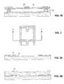
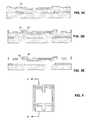
- FIGS. 1A to 1 Eare cross-sectional views illustrating one method for forming micro-mirrors
- FIG. 2is a top view of a micro-mirror showing line 1 - 1 for the cross-sectional views in FIGS. 1A to 1 E;
- FIGS. 3A to 3 Eare cross-sectional views illustrating the same method as in FIGS. 1A to 1 E but along a different cross-section;
- FIG. 4is a top view of a mirror showing line 2 - 2 for the cross-section of FIGS. 3A to 3 E;
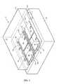
- FIG. 5is an isometric view of the assembly of two substrates, one with micromirrors, the other with circuitry and electrodes;
- FIG. 6is a cross-sectional view of the assembled device in use
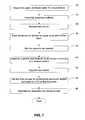
- FIG. 7is a flow chart of one method of the invention.
- FIG. 8is a top view of a wafer substrate having multiple die areas
- FIGS. 9A to 9 Gare step-by-step views of the assembly of the device.
- FIGS. 10A and 10Bare top views of two wafers that will be joined together and then singularized
- FIGS. 10C and 10Dare views of light transmissive substrates (FIG. 10A) for bonding to a wafer ( 10 D);
- FIG. 11Ais a cross-sectional view taken along line 11 - 11 of FIG. 10 upon alignment of the two wafers of FIGS. 10A and 10B, but prior to bonding;
- FIG. 11Bis a cross-sectional view taken along line 11 - 11 of FIG. 10 upon alignment of the two wafers of FIGS. 10A and 10B after bonding the two wafers, but prior to singulation;
- FIG. 12is an isometric view of a singularized wafer assembly die held on a package substrate
- FIG. 13is an illustration of a projection system having a micro-mirror device therein;
- FIG. 14Ais an illustration of a light absorbing matrix layer on the light transmissive substrate
- FIG. 14Bis an illustration of another embodiment of a light absorbing matrix layer on the light transmissive substrate
- FIG. 15is an illustration of light absorbing die frames on a light transmissive substrate
- FIGS. 16A to 16 Fare illustrations of light absorbing edges formed along micro-mirror elements
- FIG. 17is an illustration of a light absorbing grid or matrix on a light transmissive substrate with micro-mirrors on an adjacent circuit substrate;
- FIG. 18A and 18Bare illustrations of light absorbing areas formed on the wafer with circuitry thereon, wherein FIG. 18A demonstrates absorbing areas formed on the electrodes; and wherein FIG. 18B demonstrates absorbing areas between adjacent electrodes.
- light transmissiveit is meant that the material will be transmissive to light at least in operation of the device (The material could temporarily have a light absorbing layer on it to improve the ability to handle the substrate during manufacture, or a partial light absorbing layer for decreasing light scatter during use. Regardless, a portion of the substrate, for visible light applications, is preferably transmissive to visible light during use so that light can pass into the device, be reflected by the mirrors, and pass back out of the device. Of course, not all embodiments will use a light transmissive substrate).
- waferit is meant any substrate on which multiple micro-mirrors or microstructure arrays are to be formed, which allows for being divided into dies, each die having one or more micro-mirrors thereon.
- each dieis one device or product to be packaged and sold separately.
- Forming multiple “products” or dies on a larger substrate or waferallows for lower and faster manufacturing costs as compared to forming each die separately.
- the waferscan be any size or shape, though it is preferred that the wafers be the conventional rounds or substantially round wafers (e.g. 4′′, 6′′ or 12′′ in diameter) so as to allow for manufacture in a standard foundry.
- FIGS. 1A to 1 Eshow a manufacturing process for a micro-mirror structure.
- a substratesuch as glass (e.g. 1737F), quartz, PyrexTM, sapphire, (or silicon alone or with circuitry thereon) etc.
- the cross-section of FIGS. 1 A-Eis taken along line 1 - 1 of FIG. 2. Because this cross-section is taken along the hinge of the movable element, an optional block layer 12 can be provided to block light (incident through the light transmissive substrate during use) from reflecting off the hinge (or other underlying structure) and potentially causing diffraction and lowering the contrast ratio (if the substrate is transparent). This light-absorbing layer will be described in more detail in FIG. 14 to FIG. 17.
- a sacrificial layer 14such as amorphous silicon is deposited.
- the thickness of the sacrificial layercan be wide ranging depending upon the movable element/mirror size and desired tilt angle, though a thickness of from 500 ⁇ to 50,000 ⁇ , preferably around 5000 ⁇ is preferred.
- the sacrificial layercould be a polymer or polyimide (or even polysilicon, silicon nitride, silicon dioxide, etc. depending upon the materials selected to be resistant to the etchant, and the etchant selected).
- a lithography step followed by a sacrificial layeretch form holes 16 a and 16 b in the sacrificial silicon, which can be of any suitable size, though preferably having a diameter of from 0.1 to 1.5 um, preferably around 0.7 ⁇ 0.25 um.
- the etchingis performed down to the glass/quartz substrate or down to the block layer if present. Preferably if the glass/quartz layer is etched, it is in an amount less than 2000 ⁇ .
- a first layer 18is deposited by chemical vapor deposition.
- the materialcan be any suitable material, for example silicon nitride or silicon oxide deposited by LPCVD or PECVD—however polysilicon, silicon carbide (or other ceramic thin film) or an organic compound could be deposited at this point—or Al, CoSiNx, TiSiNx, TaSiNx and other ternary and higher order compounds as set forth in U.S. patent application Ser. No. 09/910,537 filed Jul. 20, 2001, and 60/300,533 filed Jun. 22, 2001 both to Reid and incorporated herein by reference (of course the sacrificial layer and etchant should be adapted to the material used).
- first layercan vary depending upon the movable element size and desired amount of stiffness of the element. However in one embodiment the layer has a thickness of from 100 to 3200 ⁇ , more preferably around 1100 ⁇ .
- the first layerundergoes lithography and etching so as to form gaps between adjacent movable elements on the order of from 0.1 to 25 um, preferably around 1 to 2 um.
- a second layer 20(the “hinge” layer) is deposited as shown in FIG. 1D.
- “hinge layer”it is meant the layer that defines that portion of the device that flexes to allow movement of the device.
- the hinge layercan be disposed only for defining the hinge, or for defining the hinge and other areas such as the mirror. In any case, the reinforcing material is removed prior to depositing the hinge material.
- the material for the second (hinge) layercan be the same (e.g. silicon nitride) as the first layer or different (e.g.
- any suitable materialsuch as silicon oxide, silicon carbide, polysilicon, or Al, CoSiNx, TiSiNx, TaSiNx or other ternary and higher compounds) and can be deposited by chemical vapor deposition like the first layer.
- the thickness of the second/hinge layercan be greater or less than the first, depending upon the stiffness of the movable element, the flexibility of the hinge desired, the material used, etc.
- the second layerhas a thickness of from 50 ⁇ to 2100 ⁇ , preferably around 500 ⁇ .
- the first layeris deposited by PECVD and the second layer by LPCVD.
- a reflective and conductive layer 22is deposited.
- the reflective/conductive materialcan be gold, aluminum or other metal, or an alloy of more than one metal though it is preferably aluminum deposited by PVD.
- the thickness of the metal layercan be from 50 to 2000 ⁇ , preferably around 500 ⁇ . It is also possible to deposit separate reflective and conductive layers.
- An optional metal passivation layer(not shown) can be added, e.g. a 10 to 1100 ⁇ silicon oxide layer deposited by PECVD. Then, photoresist patterning on the metal layer is followed by etching through the metal layer with a suitable metal etchant.
- a chlorine (or bromine) chemistrycan be used (e.g.
- both the first and second layersare deposited in the area defining the movable (mirror) element, whereas the second layer, in the absence of the first layer, is deposited in the area of the hinge.
- a plurality of layerscould be provided in place of a single layer 18 in FIG. 1C, and a plurality of layers could be provided in place of layer 20 and in place of layer 22 .
- layers 20 and 22could be a single layer, e.g.
- the reinforcing layeris removed in the area of the hinge, followed by depositing the hinge layer and patterning both reinforcing and hinge layer together.
- This joint patterning of the reinforcing layer and hinge layercan be done with the same etchant (e.g. if the two layers are of the same material) or consecutively with different etchants.
- the reinforcing and hinge layerscan be etched with a chlorine chemistry or a fluorine (or other halide) chemistry (e.g. a plasma/RIE etch with F 2 , CF 4 , CHF 3 , C 3 F 8 , CH 2 F 2 , C 2 F 6 , SF 6 , etc.
- the reinforcing layer and the hinge layercan be deposited before the first (reinforcing) and/or second (hinge) layer. Whether deposited prior to the hinge material or prior to both the hinge material and the reinforcing material, it is preferable that the metal be patterned (e.g. removed in the hinge area) prior to depositing and patterning the hinge material.
- FIGS. 3A to 3 Eillustrate the same process taken along a different cross-section (cross-section 2 - 2 in FIG. 4) and show the optional block layer 12 deposited on the light transmissive substrate 10 , followed by the sacrificial layer 14 , layers 18 , 20 and the metal layer 22 .
- the cross-sections in FIGS. 1A to 1 E and 3 A to 3 Eare taken along substantially square mirrors in FIGS. 2 and 4 respectively.
- the mirrorsneed not be square but can have other shapes that may decrease diffraction and increase the contrast ratio.
- Such mirrorsare disclosed in U.S. provisional patent application 60/229,246 to Ilkov et al., the subject matter of which is incorporated herein by reference.
- the light absorbing material on the light transmissive substratecan be made to conform to the shape of the mirrors—whether the mirrors are formed on the light transmissive substrate or on a semiconductor substrate having circuitry, electrodes and micro-mirrors thereon.
- the mirror hingescan be torsion hinges as illustrated in this provisional application.
- the sacrificial layer and release etchant disclosed hereinare exemplary only.
- a silicon dioxide sacrificial layercould be used and removed with HF (or HF/HCI), or a silicon sacrificial could be removed with CIF3 or BrF3.
- a PSG sacrificial layercould be removed with buffered HF, or an organic sacrificial such as polyimide could be removed in a dry plasma oxygen release step.
- the release etchant and sacrificial materialshould be selected depending upon the structural material to be used.
- PVD and CVDare referred to above, other thin film deposition methods could be used for depositing the layers, including spin-on, sputtering, anodization, oxidation, electroplating and evaporation.
- FIGS. 1E and 3Eshow the micro-mirrors in their released state. As can be seen in FIG. 1E, posts 24 hold the released microstructure on substrate 10 .
- each mirrorcan be formed in the same plane as the mirror element (and/or formed as part of the same deposition step) as set forth above, they can also be formed separated from and parallel to the mirror element in a different plane and as part of a separate processing step.
- This superimposed type of hingeis disclosed in FIGS. 11 and 12 of the previously-mentioned U.S. Pat. No. 6,046,840, and in more detail in U.S. patent application Ser. No. 09/631,536 to Huibers et al. filed Aug. 3, 2000, the subject matter of which being incorporated herein by reference.
- the resolutionis XGA, 1024 ⁇ 768 pixels, though other resolutions are possible.
- a pixel pitch of from 5 to 24 umis preferred (e.g. 14 um).
- the second or “lower” substrate (the backplane) diecontains a large array of electrodes on the top metal layer of the die. Each electrode electrostatically controls one pixel (one micro-mirror on the upper optically transmissive substrate) of the microdisplay. The voltage on each electrode on the surface of the backplane determines whether its corresponding microdisplay pixel is optically ‘on’ or ‘off,’ forming a visible image on the microdisplay. Details of the backplane and methods for producing a pulse-width-modulated grayscale or color image are disclosed in U.S. patent application Ser. No. 09/564,069 to Richards, the subject matter of which is incorporated herein by reference. Of course a wide variety of methods for causing actuation of the micro-mirrors are available.
- the display pixelsthemselves are preferably binary, always either fully ‘on’ or fully ‘off,’ and so the backplane design is purely digital.
- the number of reflective elements (display pixels) in each diecan be any number, such as from 6,000 to about 6 million, depending upon the desired resolution of the display. Though the micro-mirrors could be operated in analog mode, no analog capability is necessary.
- the backplane's I/O and control logicpreferably run at a voltage compatible with standard logic levels, e.g. 5V or 3.3V. To maximize the voltage available to drive the pixels, the backplane's array circuitry may run from a separate supply, preferably at a higher voltage.
- One embodiment of the backplanecan be fabricated in a foundry 5V logic process.
- the mirror electrodescan run at 0-5V or as high above 5V as reliability allows.
- the backplanecould also be fabricated in a higher-voltage process such as a foundry Flash memory process using that process's high-voltage devices.
- the backplanecould also be constructed in a high-voltage process with larger-geometry transistors capable of operating at 12V or more.
- a higher voltage backplanecan produce an electrode voltage swing significantly higher than the 5-7V that the lower voltage backplane provides, and thus actuate the pixels more robustly.
- each electrodeIn digital mode, it is possible to set each electrode to either state (on/off), and have that state persist until the state of the electrode is changed.
- a RAM-like structurewith one bit per pixel is an architecture that can accomplish this.
- One exampleis an SRAM-based pixel cell.
- Alternate well-known storage elementssuch as latches or DRAM (pass transistor plus capacitor) are also possible. If a dynamic storage element (e.g. a DRAM-like cell) is used, it is desirable that it be shielded from incident light that might otherwise cause leakage.
- a grayscale or full-color imagecan be produced by modulating pixels rapidly on and off, for example according to the method in the above-mentioned U.S. patent application Ser. No. 09/564,069 to Richards or other suitable methods.
- the backplaneallows the array to be written in random-access fashion, though finer granularity than a row-at-a-time is generally not necessary.
- the diecan be illuminated with a 200 W or more arc lamp.
- the thermal and photo-carrier effects of thismay result in special layout efforts to make the metal layers as ‘opaque’ as possible over the active circuitry to reflect incident optical energy and minimize photocarrier and thermal effects.
- some lightcan get between the mirrors or hit the mirror edges, and then scatter from one or more surfaces and end up entering the projection lens/collection optics when the dark state is desired. This has the negative effect of reducing contrast.
- non-reflective materialcan be placed on the backplane as a final layer.
- the non-reflective materialcan be a dark, opaque (e.g. black, grey or other dark color) thin film.
- materials that can be placed on backplane to absorb scattered lightinclude a non-conductive blanket film such as polyimide with carbon particles (e.g. DARC (TM) from Brewer Science).
- other dark colored ceramic filmssuch as CrN, TiAIN, TaN or other films comprising of carbon, such as amorphous CN, amorphous CAIN, TiCN, a-DLC, SiC, TiAICN, WC, etc.—preferably a non-conductive film can be used.
- conductive dark filmscould be used that are placed directly over the electrodes on the backplane and are electrically connected to the electrodes.
- a filmcould be a dark metal or metal alloy such as sputtered black chrome or niobium that has a reflectance as low as 3%.
- the black chrome coatingcan be a multilayer structure of chrome and chromium oxide (to match the index of refraction, as in an antireflective coating laminate).
- other opaque filmspreferably those with high optical density, thermally stable and with low reflectivity
- can be deposited and patternedthe opacity and color of many films being variable due to deposition parameters).
- Light absorbing conductive materials that can be deposited on the electrodesinclude black nickel, and films comprising carbon, such as a-DLC or vitreous carbon. It is also possible to deposit a dark conductive grid or matrix surrounding all of the electrodes (without electrically connecting the electrodes).
- an “anti-reflective coating”an AR film
- a normally absorptive surfacecan have enhanced absorption if an “AR film” stack (for example light transmissive dielectric layers), are placed above it so that light reflection is reduced due to destructive interference.
- AR filmfor example light transmissive dielectric layers
- Such dielectrics layerscan be designed to work particularly well at certain wavelengths and/or angles—and can be used for the matrix or frame on the light transmissive substrate, as will be discussed below.
- the upper and lower wafersare finished being processed (e.g. circuitry/electrodes on lower wafer, micro-mirrors on upper wafer), the upper and lower wafers are joined together. This joining of the two substrates allows micro-mirrors on one substrate to be positioned proximate to electrodes on the other substrate. This arrangement is illustrated in FIGS. 5 and 6, which will be described further below.
- the method for the assembly of the wafers and separation of the wafer assembly into individual diesis similar to the method for assembly of liquid crystal devices as disclosed in U.S. Pat. No. 5,963,289 to Stefanov et al, “Asymmetrical Scribe and Separation Method of Manufacturing Liquid Crystal Devices on Silicon Wafers”, which is hereby incorporated by reference.
- Many bonding methodsare possible such as adhesive bonding (e.g. epoxy, silicone, low K material or other adhesive—described further herein), anodic bonding, compression bonding (e.g. with gold or indium) metal eutectic bonding, solder bonding, fusion bonding, or other wafer bonding processes known in the art.
- the upper and lower waferare made of the same or different materials (silicon, glass, dielectric, multilayer wafer, etc.), they can first be inspected (step 30 in the flow chart of FIG. 7) for visual defects, scratches, particles, etc. After inspection, the wafers can be processed through industry standard cleaning processes (step 32 in the flow chart of FIG. 7). These include scrubbing, brushing or ultrasonic cleaning in a solvent, surfactant solution, and/or de-ionized (DI) water.
- DIde-ionized
- the mirrorsare preferably released at this point (step 34 in the flow chart of FIG. 7). Releasing immediately prior to the application of epoxy or bonding is preferable (except for an optional stiction treatment between release and bonding).
- the releasecan be in an atmosphere of xenon difluoride and an optional diluent (e.g. nitrogen and/or helium). Of course, other etchants could be used, including interhalogens such as bromine trifluoride and bromine trichloride.
- the releaseis preferably a spontaneous chemical etch which does not require plasma or other external energy to etch the silicon sacrificial layer(s). Or the release can be performed with a supercritical fluid such as set forth in U.S.
- the remainder of the deviceis treated for stiction (step 36 in the flow chart of FIG. 7) by applying an anti-stiction layer (e.g. a self assembled monolayer).
- an anti-stiction layere.g. a self assembled monolayer.
- the layeris preferably formed by placing the device in a liquid or gas silane, preferably a halosilane, and most preferably a chlorosilane.
- silanesare known in the art for their ability to provide anti-stiction for MEMS structures, including the various trichlorsilanes set forth in “Self Assembled Monolayers as Anti-Stiction Coatings for MEMS: Characteristics and Recent Developments”, Maboudian et al., as well as other unfluorinated (or partially or fully fluorinated) alkyl trichlorosilanes, preferably those with a carbon chain of at least 10 carbons, and preferably partially or fully fluorinated. (Tridecafluoro-1,1,2,2-tetrahydro-octyl)trichlorosilane available from Gelest, Inc. is one example. Other trichlorosilanes (preferably fluorinated) such as those with phenyl or other organic groups having a ring structure are also possible.
- spacersare mixed into sealant material (step 38 in the flow chart of FIG. 7).
- Spacers in the form of spheres or rodsare typically dispensed and dispersed between the wafers to provide cell gap uniformity and space for mirror deflection. Spacers can be dispensed in the gasket area of the display and therefore mixed into the gasket seal material prior to seal dispensing. This is achieved through normal agitated mixing processes.
- the final target for the gap between the upper and lower wafersis preferably from 1 to 10 um, though other gaps are possible depending upon factors such as micro-mirror size and deflection angle.
- the spheres or rodscan be made of glass or plastic, preferably an elastically deforming material.
- spacer pillarscan be fabricated on at least one of the substrates.
- pillars/spacersare provided only at the side of the array.
- pillars/spacerscan be fabricated in the array itself.
- Other bonding agents with or without spacerscould be used, including anodic bonding or metal compression bonding with a patterned eutectic or metal.
- a gasket seal materialcan then be dispensed (step 40 in the flow chart of FIG. 7) on the bottom substrate in a desired pattern, usually in one of two industry standard methods including automated controlled liquid dispensing through a syringe and printing (screen, offset, or roller).
- a syringeWhen using a syringe, it can be moved along X-Y coordinates relative to the parts.
- the syringe tipis constrained to be just above the part with the gasket material forced through the needle by positive pressure.
- Positive pressurecan be provided either by a mechanical plunger forced by a gear driven configuration and/or by an air piston and/or pressed through the use of an auger.
- many different adhesive dispensing methodscan be used.
- the two wafersare aligned (step 42 in the flow chart of FIG. 7) preferably to within 1 micron accuracy or less. Alignment of the opposing electrodes or active viewing areas is aided by registration of substrate fiducials on opposite substrates. This task can be accomplished with the aid of video cameras with lens magnification.
- the machinesrange in complexity from manual to fully automated with pattern recognition capability.
- the final cell gapcan be set by pressing (step 44 in the flow chart of FIG. 7) the previously tacked laminates in a UV or thermal press.
- a UV pressa common procedure would have the substrates loaded into a press where at least one or both of the press platens are quartz, in order to allow UV radiation from a UV lamp to pass unabated to the gasket seal epoxy.
- Exposure time and flux ratesare process parameters determined by the equipment and adhesive materials.
- Thermally cured epoxiesrequire that the top and bottom platens of a thermal press be heated. The force that can be generated between the press platens is typically many pounds. With thermally cured epoxies, after the initial press the arrays are typically transferred to a stacked press fixture where they can continually to be pressed and post-cured for 4-8 hours.
- the assemblycan be separated into individual dies (step 46 in the flow chart of FIG. 7). Silicon substrate and glass scribes are placed on the respective substrates in an offset relationship at least along one direction. Or, the substrates can be provided initially with scribes on them already. The units are then separated, resulting in each unit having a bond pad ledge on one side and a glass electrical contact ledge on an opposite side—if such an offset arrangement is desired.
- the partsmay be separated from the array by any of the following methods.
- the order in which the array (glass first) substrate is scribedis important when conventional solid-state cameras are used for viewing and alignment in a scribe machine.
- the scribe toolis aligned with the scribe fiducials and processed.
- the resultant scribe lines in the glasscan be used as reference marks to align the silicon substrate scribe lanes. These scribe lanes may be coincident with the glass substrate scribes or uniformly offset.
- the partsare then separated from the array by venting the scribes on both substrates. Automatic breaking is done by commercially available guillotine or fulcrum breaking machines. The parts can also be separated by hand. Or, any other suitable singularization method can be used to separate the bonded wafers into bonded wafer die portions.
- separationmay also be done by glass scribing and partial sawing of the silicon substrate.
- Sawingrequires an additional step at gasket dispense.
- Sawingcan be performed in the presence of a high-pressure jet of water. Moisture should preferably not be allowed in the area of the fill port or damage of the MEMS structures could occur. Therefore, at gasket dispense, an additional gasket bead must be dispensed around the perimeter of the wafer.
- the end of each scribe/saw lanemust be initially left open, to let air vent during the align and press processes. After the array has been pressed and the gasket material cured, the vents are then closed using either the gasket or end-seal material.
- the glassis then aligned and scribed as described above. Sawing of the wafer is done from the backside of the silicon where the saw streets are aligned relative to the glass scribe lanes described above. The wafer is then sawed to a depth of 50%-90% of its thickness. The parts are then separated as described above.
- both the glass and silicon substratesmay be partially sawed prior to part separation.
- vent and seal processes as described abovesaw lanes are aligned to fiducials on the glass substrates.
- the glassis sawed to a depth between 50% and 95% of its thickness.
- the silicon substrateis sawed and the parts separated as described above.
- each die area 3(having a length A and a height B) comprises one or more (preferably released) micro-mirrors.
- each diepreferably has at least 1000 movable mirrors, and more likely between 1 and 6 million movable elements.
- each die area 3 a to 3 dcomprises one or more micro-mirrors, which have already been released in a suitable etchant.
- epoxycan be applied in the form of beads 51 a to 51 d along each side of the die area, or as beads 53 a to 53 d at each corner of the die area.
- epoxy ribbons 55 a and 55 bcould be applied along two sides of each die, or a single ribbon 57 could be applied substantially surrounding an entire die.
- the dienot be fully surrounded with an epoxy gasket, as this will prevent air or other gas from escaping when the two wafers are pressed together during a full or partial epoxy cure.
- a common epoxy application methodthroughout the entire wafer (the different types of applications in FIG. 9B are for illustrations purposes only).
- the areas in which epoxy is appliedcan first have a sacrificial material deposited in that area (preferably in an area larger than the bead or band of epoxy due to expansion of the epoxy under compression).
- the sacrificial materialcould also be applied to the entire wafer except in areas having micro-mirrors thereon.
- a conductive epoxy(or other adhesive) could be used in order to make electrical contact between the wafer having circuitry and electrodes and the wafer having MEMS thereon.
- upper wafer 25 and the lower substrate wafer 5 with micromirrors (and optionally circuitry)are brought into contact with each other.
- the final gap between the two waferscan be any size that allows the two wafers to be held together and singularized uniformly. Because gasket beads will expand upon application of pressure (thus taking up valuable real estate on a wafer with densely positioned die areas), it is preferable that the gap size be larger than 1 um, and preferably greater than 10 um.
- the gap sizecan be regulated by providing microfabricated spacers or spacers mixed in with the epoxy (e.g. 25 um spacers). However, spacers may not be necessary depending upon the type of microstructure and the amount of pressure applied.
- FIG. 9Dshows the lower wafer 5 and upper wafer 25 bonded together.
- Horizontal and vertical score or partial saw lines 21 a and 21 bare provided on both the upper wafer 25 and the first (lower) wafer 5 (lines not shown on wafer 5 ).
- the score lines on the two wafersare offset slightly from each other at least in one of the (horizontal or vertical). This offset scoring or partial sawing allows for ledges on each die when the wafer is completely singularized into individual dies (see FIG. 9E). Electrical connections 4 on ledge 6 on die 3 c allow for electrical testing of the die.
- FIG. 5a top perspective view of a portion of a bonded wafer assembly die 10 is illustrated.
- the mirror shapes illustrated in FIGS. 1 to 5are exemplary, as many other mirror structures are possible, such as set forth in U.S. patent application Ser. No. 09/732,445 to Ilkov et al. filed Dec. 7, 2000, incorporated herein by reference.
- the pixel cells 54 , 54 a , 54 b and 54 chave a pixel pitch of, for example, 12 microns. “Pixel pitch” is defined as the distance between like portions of neighboring pixel cells.
- Reflective deflectable elementse.g., mirrors 48 , 48 a , 48 b and 48 c , each corresponding to a respective pixel cell 54 , 54 a , 54 b and 54 c , are attached to the lower surface 14 of the optically transmissive substrate 52 in an undeflected position.
- mirrors 48 , 48 a , 48 b and 48 care visible through optically transmissive substrate 52 in FIG. 5.
- light blocking aperture layers 56if present, between the mirrors 48 , 48 a , 48 b or 48 c and the optically transmissive substrate 52 , are represented only by dashed lines so as to show underlying hinges 50 , 50 a , 50 b and 50 c .
- the distance separating neighboring mirrorsmay be, for example, 0.5 microns or less.
- the optically transmissive substrate 52is made of materials, which can withstand subsequent processing temperatures.
- the optically transmissive substrate 52may be, for example, a 4 inch quartz wafer 500 microns thick. Such quartz wafers are widely available from, for example, Hoya Corporation U.S.A at 960 Rincon Circle, San Jose, Calif. 95131.
- the substratecan be glass such as Coming 1737 or Coming Eagle2000 or other suitable optically transmissive substrate.
- the substrateis transmissive to visible light, and can be display grade glass.
- the light transmissive substrate 52is bonded to e.g. a MOS-type substrate 62 (a semiconductor substrate can be used such as a silicon substrate with circuitry and electrodes formed thereon) in spaced apart relation due to spacers 66 .
- a plurality of electrodes 63are disposed adjacent a plurality of micro-mirrors 64 (mirrors simplified and only 9 illustrated for convenience) for electrostatically deflecting the micromirrors.
- An incoming light beam 65 awill be reflected by a non-deflected mirror at the same angle as it is incident, but will be deflected “vertically” as outgoing light beam 65 b when the mirror is deflected.
- FIG. 13A simplified schematic of one type of projection system is illustrated in FIG. 13, where a light source 110 , e.g. an arc lamp having a reflector 120 , directs light through a color sequencer (e.g.
- color wheel 130that rotates around axis of rotation 170 via motor 140 ), after which the light enters light pipe 150 and optics 160 so as to be incident on a micro-mirror array 180 and is reflected off of the micro-mirrors of the array and projected via projection optics 190 to a target 210 .
- the method for forming micro-mirrors as set forth aboveis but one example of many methods for forming many different MEMS devices (whether with or without an electrical component), in accordance with the present invention.
- the electrical component of the final MEMS deviceis formed on a separate wafer than the micro-mirrors in the above example, it is also possible to form the circuitry and micro-mirrors monolithically on the same substrate.
- the method for forming such micro-mirrorscould be similar to the methods described herein (with the difference being that the mirrors are formed on the substrate after forming circuitry and electrodes). Or, other methods for forming circuitry and micro-mirrors monolithically on the same substrate as known in the art could be used.
- FIG. 10Ais a top view of a light transmissive cover wafer (having a mask area, getter area, lubricant area and compression metal bonding area)
- FIG. 10Bis an illustration of such a monolithically formed mirror array (e.g. for a spatial light modulator) on a bottom semiconductor wafer (along with a metal area for compression bonding).
- a plurality of mirror arrays 71 a to 71 eis formed on a “bottom” wafer 70 (e.g. a silicon wafer).
- a metal for compression bondingis applied (areas 73 a to 73 e ) around each mirror array.
- more arrayscould be formed on the wafer (as shown in FIG. 8).
- a “top” wafer 80e.g. glass or quartz—preferably display grade glass
- masks 81 a -ewhich will block visible light around a perimeter area of each die from reaching the mirror arrays after the two wafers are bonded and singularized.
- Also illustrated in FIG. 10Aare areas of lubricant 83 a - e , areas of getter material 85 a - e , and areas of metal for compression bonding 87 a - e . If the wafer of FIG.
- a lubricant on the wafer of FIG. 10Amay be omitted if desired (although multiple applications of lubricants can be provided).
- the lubricant applied to the wafer as a gasket, band or drop on the wafercan be any suitable lubricant, such as the various liquid or solid organic (or hybrid organic-inorganic materials) as known in the art.
- a trichlorosilane SAMis applied to the entire wafer or large portions of the wafer at least covering the micro-mirror elements, and a silicone is applied to the lubricant areas 83 a - e .
- the metal for compression bondingcould be any suitable metal for this purpose such as gold or indium.
- the adhesivecould be any suitable adhesive, such as an epoxy or silicone adhesive, and preferably an adhesive with low outgassing).
- any combination of these elementscould be present (or none at all if the bonding method is other than an adhesive bonding method).
- one or more of the mask, lubricant, getter and bonding materialare present on the “top” wafer 80 prior to bonding.
- the lubricant, getter and bonding materialcould be applied to only the top or bottom wafer or both wafers.
- the lubricant and gettermay be desirable to apply to the bottom wafer around the circuitry and electrodes, with bonding material on both wafers.
- the maskor the lubricant or getter
- the bands of lubricant, getter and bonding materialneed not fully encircle the “die area” on the wafer, but could be applied in strips of dots as illustrated in FIG. 9B.
- the bonding materialdoes not fully encircle the MEMS die area, then, prior to singulation, it is preferred that the bonding material “gap” be filled so as to protect the MEMS devices during singulation (from particulate and/or liquid damage depending upon the singulation method).
- substrates 101 a to 101 dare substrates transmissive to visible light and have thereon masks 81 a to 81 d as well as areas of lubricant 83 a to 83 d , areas of getter material 85 a to 85 d , and areas of bonding material 87 a to 87 d (e.g. gold or indium for metal compression bonding.
- the mask areasare preferably “picture frame” shaped rectangular areas that block the transmission of visible light. This arrangement is desirable for selectively blocking light incident on micro-mirror arrays formed on the wafer. After bonding the multiple substrates with mask areas to the wafer, the wafer is singularized into wafer assembly portions, followed by packaging such as in FIG. 12.
- the MEMS waferscould be made of any suitable material, depending upon the final application for the devices, including silicon, glass, quartz, alumina, GaAs, etc. Silicon wafers can typically be processed to include circuitry.
- the “top” wafer of FIG. 10Ais preferably transparent, as mentioned above.
- the mask illustrated in FIG. 10Acan be an absorptive or reflective mask, such as one made from TiN, AIN, or other oxide or nitride compound, or polymers or other suitable materials having sufficient light absorbing capabilities.
- This “top” wafercould also incorporate other optical elements, such as lenses, UV or other types of filters or antireflection and/or antiscratch coatings.
- FIG. 11Ais a cross-section taken along line 11 - 11 in FIG. 10A (after alignment with bottom wafer 70 in FIG. 10B), whereas FIG. 10B is the same cross-section after bonding (but before singulation).
- FIG. 12is an illustration of a packaged wafer assembly portion after singularization of the bonded wafers. As can be seen in FIG. 12, a lower substrate 94 is bonded to the upper substrate 93 , with the lower substrate held on a lower packaging substrate 90 .
- Metal areas 96 on lower wafer portion 94will be electrically connected to metal areas 97 on the package substrate 90 .
- the wafer assembly dieformed of substrates 93 and 94 , as the MEMS elements are already protected within the wafer assembly (though a “second” package surrounding the substrate assembly could be used for added protection and hermeticity).
- the diecomprised of two-bonded die substrates (light transmissive and semiconductor, for example, with MEMS elements on the light transmissive substrate) seal (preferably hermetically) the MEMS elements from ambient.
- a micro-mirror arraycomprised of micro-mirrors held on a first substrate (preferably glass and more preferably display quality glass) which substrate is bonded to a semiconductor substrate (preferably silicon) which in turn is bonded to a lower package substrate that does not fully encapsulate the bonded die substrates (because the light transmissive and semiconductor substrates already encapsulate the MEMS elements) is a less expensive alternative to standard packaging of micro-mirror arrays for projection displays. Also, such a packaging arrangement allows for providing anti-stiction treatment, getters etc. at the wafer level further decreasing costs of packaging the device. Of course, an additional package surrounding the substrate assembly could also be used.
- a fully surrounding packagehaving an optically transmissive window for light to enter and exit the package.
- a fully surrounding packagecould be a hermetic package with, for example, a pressure less than ambient pressure.
- the pressure between the bonded die substrates hermetically sealed togethercan be less than 1 atm, preferably less than 0.25 atm, and more preferably less than Torr. If very low pressures are desired, then pressures between the substrates of less than 10 Torr, less than 1 Torr or even as low as 100 mTorr can be used. Getters, lubricants, etc. could be disposed within this surrounding package rather than within the bonded substrates.
- the light transmissive wafer 80e.g. glass or quartz—preferably display grade glass
- masks 81 a to 81 ewhich will block visible light around a perimeter area of each die from reaching the mirror arrays after the two wafers are bonded and singularized.
- This “frame” of light absorbing materialis preferably one that absorbs many wavelengths in the visible spectrum.
- An opaque material, preferably a black materialis preferred for the mask around the perimeter of each die.
- Such frames or “masks” around each micro-mirror arrayare shown in FIG. 15.
- a light transmissive substrate 102is provided with light blocking/absorbing frame areas 100 that surround each die area 101 on the substrate 102 .
- the material that forms the dark frame area 100can be thin film deposited by CVD, PVD etc. and patterned to form the frame areas around each die area on the wafer.
- ion beam sputtered black chrome or niobiumis used, that has a reflectance as low as 3% through the light transmissive substrate, with high thermal stability. After sputtering the film onto e.g. glass, it is etched to form the “frames” in each die area.
- the black chrome coatingcan be a multilayer structure of chrome and chromium oxide (to match the index of refraction, as in an antireflective coating laminate).
- opaque filmspreferably those with high optical density, thermally stable and with low reflectivity
- Light absorbing materialscan be used such as black nickel, CrN, TiAlN, TaN and many films comprising carbon, such as amorphous CN, amorphous CAIN, TiC, TiCN, a-DLC, vitreous carbon, SiC, TiAlCN, WC, etc.
- Multilayer structuressuch as TiC/WC, WC/C or TiAlN/WC/C, can be used, as well as other multilayer structures with matched indices.
- polyimides and other polymers containing carbon blackcan be used. If the light-absorbing layer is exposed to an etchant at the time of release of the micro-mirrors, the light absorbing material should preferably be resistant to the etchant used.
- Forming the light absorbing areascan be by any suitable film forming method—such as standard deposition and patterning techniques.
- the metals and metal alloyscan be deposited by sputtering a target in an inert atmosphere. Other techniques, such as electroplating can be used.
- a targetcan be reactively sputtered such as in a nitrogen atmosphere to form nitride ceramic films. Or, some films can be deposited by chemical vapor deposition as known in the art. Patterning of the films to form matrices, bands, strips or other designs can be by any suitable etching chemistry—such as by a chlorine (plasma) etch after deposition and patterning of a photoresist. It is also possible to deposit and pattern a photoresist followed by deposition of the light absorbing material.
- etching chemistrysuch as by a chlorine (plasma) etch after deposition and patterning of a photoresist. It is also possible to deposit and pattern a photoresist followed by deposition of the light absorbing
- each die area( 101 in FIG. 15) will be formed an array of micro-mirrors—possibly thousands or millions of such mirrors in each die area—depending upon the desired resolution of the image reflected from such micro-mirror array.
- a frame of light absorbing materialsuch as that disclosed above for surrounding each die area, can be provided on the light transmissive substrate to surround the area where each micro-mirror will be formed on the light transmissive substrate. Whereas the frame areas surrounding each die (such as in FIG.
- micro-mirror framesare illustrated in FIGS. 14A and 14B as a light absorbing matrix 98 on a substrate 99 —where thousands or millions of such frames illustrated in FIGS. 14A and 14B can be disposed within a single light absorbing frame of FIG. 15. Or course it is not necessary that both micro-mirror frames of FIG. 14 and die frames of FIG. 15 be provided together.
- the materials used to form the micro-mirror framescan be those such as set forth above in relation to die frames and can include an AR coating (the AR coating can also cover the entire light transmissive substrate if desired.
- the “frames” around the micro-mirrors and around the die areas (the micro-mirror array areas)can instead be provided in the form of strips or bands—where the light blocking or absorbing material is provided along some but not all sides of the micro-mirrors (or micro-mirror arrays). Also, though the light absorbing material is preferably provided on the same side of the light transmissive substrate as the micro-mirrors, it is also possible to deposit the light absorbing material on the side of the light transmissive substrate opposite from the formed micro-mirrors.
- the light absorbing materialis provided between the micro-mirrors and on the same side as the micro-mirrors, it can be deposited so as to be in the area of impact of the micro-mirrors on the light transmissive substrate. Such impacting of the micro-mirrors on the light transmissive substrate is discussed in detail in U.S. Pat. Nos. 6,356,378, 6,046,840 and 6,172,797 incorporated herein by reference. If the light absorbing strips or frames are disposed at such impact point of the micro-mirror, then preferably such material is a hard and at least minimally electrically conductive to allow dissipation of charge that builds up due to repeated impact of the micro-mirrors.
- the light absorbing areasare provided on the same substrate as the micro-mirrors.
- a circuit substratee.g. a silicon substrate having thereon circuitry, electrodes and micro-mirrors.
- the light absorbing layersare provided on a separate light transmissive substrate that is held spaced apart from the circuit substrate—though preferably at a small distance such as 75 microns or less, preferably 50 microns or less, and more preferably at a closer distance e.g. less than 10 microns. It is possible to position the light transmissive substrate at a distance of from 1 to 5 microns. A close relationship between the light transmissive substrate and the micro-mirrors can allow for better blocking of light between adjacent micro-mirrors.
- FIG. 17An example of such an arrangement is illustrated in FIG. 17.
- a substrate 122e.g. a silicon substrate
- circuitry and electrodes thereon(not shown) has formed above the circuitry and electrodes an array of micro-mirrors 129 .
- FIG. 17for ease of illustration only a few micro-mirrors are shown along the length of the mirror array—of course an actual mirror array would likely have hundreds or thousands of micro-mirrors along one dimension of the array—depending upon the desired resolution of the projection display.
- FIG. 17for ease of illustration only a few micro-mirrors are shown along the length of the mirror array—of course an actual mirror array would likely have hundreds or thousands of micro-mirrors along one dimension of the array—depending upon the desired resolution of the projection display.
- each micro-mirrorwould have two electrodes disposed on the substrate below for tilting the micro-mirror in opposite directions depending upon which electrode causes electrostatic attraction of the adjacent micro-mirror.
- electrodesdisposed on the substrate below for tilting the micro-mirror in opposite directions depending upon which electrode causes electrostatic attraction of the adjacent micro-mirror.
- other arrangementssuch as micro-mirrors pivotable towards the substrate in a single direction, could be used.
- Substrate 120is a light transmissive substrate, such as a plastic, glass or quartz substrate—preferably a display grade glass substrate.
- a frame 123that surrounds the micro-mirror array.
- Frame 123in many cases will be a frame disposed as a rectangular thin film but it is also possible for a material that acts as a spacer to space the substrates 120 and 122 apart, or as a bonding agent, to be opaque and act as the frame surrounding the micro-mirror array.
- Also disposed on substrate 120are light absorbing areas 126 that are disposed between the micro-mirrors 129 when the two substrates are disposed adjacent each other.
- the light absorbing areas 126can be in the form of strips or other patterns, it is preferred that the light absorbing areas are a grid or matrix that allows light to pass in areas where the micro-mirrors are disposed, but blocks light in areas corresponding to gaps between the micro-mirrors.
- the materials for forming the light absorbing areas 123 and 126can be as in the other embodiments hereinabove. Also, substrates 120 and 122 can be bonded directly together or indirectly via packaging or other structure.
- the substratesare bonded together at the wafer level by a) bonding e.g. a glass wafer and a silicon wafer together and then singularizing into dies, or b) bonding glass (or other light transmissive material) dies or caps having the light absorbing strips or grids to a semiconductor (or other circuit containing) wafer and then singularizing the semiconductor wafer. It is preferred that the substrates 120 and 122 be disposed close to each other (or, if substrate 120 is in the form of a concave “cap”, then the area of the cap having the matrix be disposed close to substrate 122 ).
- the substratesare disposed at a distance of less than 75 microns, and more preferably less than 50 microns. Or course, closer distances are easily achieved particularly if the two substrates are bonded together. Substrate distances of 10 microns or less can be achieved, or even 5 microns or less if desired.
- the light transmissive substratee.g. a glass or quartz wafer
- the semiconductorsilicon substrate with circuitry
- the light transmissive substrateis bonded directly to the semiconductor substrate—allowing a close gap between the two substrates. Bonding the two substrates at the wafer level also allows for protecting the micro-mirrors during wafer singulation into dies—such as set forth in U.S. patent application Ser. No. 10/005,308 to Patel et al. filed Dec. 3, 2001, incorporated herein by reference.
- a substrate 111(this can be a light transmissive substrate such as glass, or a semiconductor substrate with actuation circuitry thereon) is provided on which is deposited a sacrificial layer 112 , which can be of any suitable material such as those sacrificial materials disclosed elsewhere herein. After depositing sacrificial layer 112 , mirror layer 113 is formed.
- Mirror layer 113can be a single layer of a reflective material, such as a metal, metal alloy or metal compound, or a laminate of structural materials, where preferably one of the layers is reflective. On layer(s) 113 is deposited light absorbing layer 114 . Each of the layers in FIG. 16A can be patterned prior to depositing the next layer (or patterned together with adjacent layers, depending upon the material of the adjacent layers). And, it should be noted that FIGS. 16A and 16B are simplified views—additional layers such as hinge layers above or below the mirror plate 113 (depending upon whether substrate 111 is light transmissive or not) would also generally be provided if the hinge is not formed in the same layer as the mirror plate.
- light-absorbing layer 114is directionally etched removing almost all of the light-absorbing layer except for strips of light absorbing material 114 a and 114 b along sides of the mirror plate 113 .
- a hinged reflective micro-mirror element having non-reflective light absorbing edgesis formed, pivotably suspended above substrate 111 .
- the light absorbing mirror edgesare preferably dark colored, preferably black.
- the light absorbing mirror edgescan be formed with deposition followed by directional etching as mentioned above, use of photoresist to selectively deposit the light absorbing material only around the edges of the micro-mirror (or along the edges and “backside” of the micro-mirror), or using photoresist for etching the light absorbing layer, can be performed. Many different combinations of materials and deposition and patterning methods can be employed.
- the periphery of the reflective surface proximate to the edges or sidewallscan also be coated with light absorbing materials, as shown in FIG. 16D. In this way, scattered light from defects and/or roughness near the edges may thus be reduced, if not eliminated.
- the backside surface opposite to the reflective surface for reflecting incident lightcan also increase scattered light, which scattered light can be collected by the projection lens or lenses of the projection system, thus reducing the contrast ratio.
- the backside surface of the micro-mirrorcan then be covered with a light-absorbing layer, for example, layer 114 C in FIG. 16E. It is also possible to cover the periphery of the micromirror surface, the edges or sidewalls and/or the underside of the micromirror, such as can be seen in FIG. 16F.
- FIGS. 18A and 18Billustrate the backplane to reduce the scattered light from the backplane.
- electrodes 63can be covered with light-absorbing materials 67 .
- FIG. 18Billustrates that all electrodes are covered with light-absorbing material 67 , however, this is not necessary. Instead, this substrate can be selectively covered with the light-absorbing material as appropriate.
- light-absorbing strips 68can be deposited in the spaces between adjacent electrodes 63 , as shown in FIG. 18B. The scattered light from these spaces can thus be reduced, if not eliminated.
- electrodes and the spaces between adjacent electrodescan be selectively covered with light-absorbing materials either individually or in combination as appropriate (not shown).
- the light transmissive substrate bonded to the semiconductor substratehermetically seals the MEMS elements from the surrounding environment, and preferably at a pressure lower than the surrounding environment.
- the two substratesdies or wafers
- the two substratesare bonded together at subatmospheric pressure and hermetically sealed (followed by wafer singulation if performed at the wafer level).
- the two substratescould be bonded at ambient pressure, though not hermetically, followed by a second seal at a lower pressure that hermetically seals off the interior of the bonded substrates from the surrounding environment.
- the two substratesare first bonded with an adhesive (e.g.
- an anti-stiction agentis deposited on the MEMS elements after release, but before bonding the substrates together, it may be desirable to protect the areas that will be required for bonding (e.g. if an adhesive is used—protecting those areas where the adhesive will be applied), followed by application of the anti-stiction agent, in turn followed by removing the protecting agent or film, followed in turn by application of the bonding agent.
- a filmcould be applied in strips or rings that correspond to the location of the later applied bonding agent, and could be a photoresist or an inorganic thin film applied by CVD or sputtering.
- the MEMS elementscould be released, followed by application of an anti-stiction agent. Then, the applied anti-stiction agent (e.g.
- a self assembled monolayer formed from chlorosilane or alkoxysilane precursorsis removed in the areas where the bonding agent will be applied (in any pattern—though preferably circumferentially around the micro-mirror array if the MEMS elements are micro-mirrors in an array). Removal can be accomplished by laser ablation (preferably focusing laser above the substrate), particle beam, application of a stripping chemical (e.g. acetone) or even mechanical removal (scoring with a hard or soft object or with a polishing wheel).
- a stripping chemicale.g. acetone
- epoxycan be applied to the one or both of the upper and lower wafers.
- epoxyis applied to both the circumference of the wafer and completely or substantially surrounding each die/array on the wafer.
- Spacerscan be mixed in the epoxy so as to cause a predetermined amount of separation between the wafers after bonding. Such spacers hold together the upper and lower wafers in spaced-apart relation to each other. The spacers act to hold the upper and lower wafers together and at the same time create a space in which the movable mirror elements can move.
- the spacer layercould comprise walls or protrusions that are micro-fabricated.
- one or more waferscould be bonded between the upper and lower wafers and have portions removed (e.g. by etching) in areas corresponding to each mirror array (thereby providing space for deflection of the movable elements in the array).
- the portions removed in such intermediate waferscould be removed prior to alignment and bonding between the upper and lower wafers, or, the wafer(s) could be etched once bonded to either the upper or lower wafer.
- the spacersare micro-fabricated spacers, they can be formed on the lower wafer, followed by the dispensing of an epoxy, polymer, or other adhesive (e.g. a multi-part epoxy, or a heat or UV-cured adhesive) adjacent to the micro-fabricated spacers.
- the adhesive and spacersneed not be co-located, but could be deposited in different areas on the lower substrate wafer.
- a compression bond materialcould be used that would allow for adhesion of the upper and lower wafers.
- the spacerscould be balls or rods of a predetermined size that are within the adhesive when the adhesive is placed on the lower wafer.
- Spacers provided within the adhesivecan be made of glass or plastic, or even metal so long as the spacers do not interfere with the electrostatic actuation of the movable element in the upper wafer.
- the spacersare preferably from 1 to 250 microns, the size in large part depending upon the size of the movable mirror elements and the desired angle of deflection.
- the spacer size in the direction orthogonal to the plane of the upper and lower wafersis more preferably from 1 to 100 microns, with some applications benefiting from a size in the range of from 1 to 20 microns, or even less than 10 microns.
- a sticking force reducing agentcan be applied to the micro-mirrors on the wafer to reduce adhesion forces upon contact of the micro-mirrors with another layer or structure on the same or opposing substrate.
- adhesion reducing agentsare known, in the present invention the agent is preferably applied to the wafer before wafer bonding (or after wafer bonding but before singulation), rather than to the singularized die or package for the die.
- adhesion reducing agentsincluding various trichlorosilanes, and other silanes and siloxanes as known in the art for reducing stiction for micro electromechanical devices, as mentioned elsewhere herein.
- a getter or molecular scavengercan be applied to the wafer prior to wafer bonding as mentioned above.
- the gettercan be a moisture, hydrogen, particle or other getter.
- the getter(s)is applied to the wafer around the released MEMS structures (or around, along or adjacent an array of such structures, e.g. in the case of a micro-mirror array), of course preferably not being in contact with the released structures.
- a metal oxide or zeolitecan be the material utilized for absorbing and binding water (e.g. StayDry SD800, StayDry SD1000, StayDry HiCap2000—each from Cookson Electronics).
- a combination gettercould be used, such as a moisture and particle getter (StayDry GA2000-2) or a hydrogen and moisture getter (StayDry H2-3000).
- the gettercan be applied to either wafer, and if adhesive bonding is the bonding method, the getter can be applied adjacent the epoxy beads or strips, preferably between the epoxy and the micromirrors, and can be applied before or after application of the adhesive (preferably before any adhesive is applied to the wafer(s).
- a getter(or getters if more than one type of getter is used) is provided in a trench or other cavity formed in either (or both) substrates.
- a trench extending along one or more sides of a micro-mirror arraycould be formed prior to depositing the sacrificial layer and thin films (or at the end before or after release of the micro-mirrors).
- a trench (or cavity)could be formed in a silicon substrate (e.g. with circuitry and electrodes thereon if formed as the dual substrate approach set forth above, or circuitry, electrodes and micro-mirrors thereon if formed monolithically).
- a trench or cavity for the getter(s)could be formed in the glass substrate. It is also possible to form a trench or cavity in both substrates with the same or different getters deposited therein.
- the first waferis preferably glass, borosilicate, tempered glass, quartz or sapphire, or can be a light transmissive wafer of another material.
- the second wafercan be a dielectric or semiconductor wafer, e.g. GaAs or silicon.
- the first and second wafersare bonded together with an adhesive (though metal or anodic bonding are also possible), depending upon the MEMS structure and the type of micromachining.
- the releasingcan be performed by providing any suitable etchant, including an etchant selected from an interhalogen, a noble gas fluoride, a vapor phase acid, or a gas solvent. And, the releasing is preferably followed by a stiction treatment (e.g. a silane, such as a chlorosilane). Also, a getter can be applied to the wafer before or after the adhesion reducing agent is applied, and before or after an adhesive is applied (if an adhesive bonding method is chosen). Preferably the time from releasing to bonding is less than 12 hours, and preferably less than 6 hours.
- a stiction treatmente.g. a silane, such as a chlorosilane
- a gettercan be applied to the wafer before or after the adhesion reducing agent is applied, and before or after an adhesive is applied (if an adhesive bonding method is chosen).
- the time from releasing to bondingis less than 12 hours, and preferably less than 6 hours.
Landscapes
- Engineering & Computer Science (AREA)
- Microelectronics & Electronic Packaging (AREA)
- Chemical & Material Sciences (AREA)
- Physics & Mathematics (AREA)
- General Physics & Mathematics (AREA)
- Nanotechnology (AREA)
- Computer Hardware Design (AREA)
- Manufacturing & Machinery (AREA)
- Power Engineering (AREA)
- Composite Materials (AREA)
- Condensed Matter Physics & Semiconductors (AREA)
- Materials Engineering (AREA)
- Crystallography & Structural Chemistry (AREA)
- Optics & Photonics (AREA)
- Mechanical Light Control Or Optical Switches (AREA)
Abstract
Description
- The invention is related generally to spatial light modulators, and, more particularly, to spatial light modulators with light absorbing areas that reduce light from passing through a light transmissive substrate—such as around the periphery of an array of pixels in a spatial light modulator.[0001]
- Spatial Light Modulators (SLMs) are transducers that modulate an incident beam of light in a spatial pattern that corresponds to an optical or electrical input. A type of SLM is the SLM based on Micro Electro-Mechanical Systems (MEMS). A typical MEMS-based SLM consists of an array of micro-mirrors mounted on movable elements. Each individual micro-mirror can be independently deflected by an electrostatic force. Reflection of a beam of incident light impinging a micro-mirror can then be controlled, for example by deflecting the micro-mirror through changing the electrostatic force applied to the micro-mirror. MEMS-based SLMs have experienced significant developments and been innovatively implemented in many applications, one of which is the use in digital display systems. In a display application, each micro-mirror is associated with a pixel of a displayed image. To produce a bright pixel, the state of the micro-mirror associated with the pixel is set in such a way that the reflected light from the micro-mirror is directed onto a target for viewing. And to produce a dark pixel, the status of the micro-mirror is tuned such that the reflected light from the micro-mirror is directed away from the display device. In order to display a black-and-white image, the micro-mirror array is illuminated by a beam of light. By coordinating the reflective status of the micro-mirrors based on the brightness of the pixels of the desired image, the collective effect of all reflected lights from individual micromirrors is the generation of the desired image. Gray-scaled and colored-images can also be displayed using the micro-mirror array with the pulse-width-modulation and sequential-color-display techniques, which will not be discussed in detail herein.[0002]
- Currently, varieties of MEMS-based SLMs have been developed. Regardless of the differences, the function of the MEMS-based SLMs for display is based on the reflection of light from individual micro-mirrors. Therefore, the quality of the displayed image strongly depends on the reflections of the micro-mirrors.[0003]
- There are many things that define the quality of a displayed image. Contrast ratio is a major determinant of perceived image quality. Contrast ratio is the ratio of luminance between the brightest white that can be produced and the darkest black that can be produced. If a displayed image has high contrast ratio, a viewer will judge it to be sharper than a displayed image with lower contrast ratio, even if the lower contrast image has substantially more measurable resolution. Contrast ratio of a displayed image from a MEMS-based SLM can be seriously degraded by light scattered, for example, from the edges of the micro-mirrors and the structures below the micro-mirrors. This scattered light typically travels through the projection lens of the display device and is directed on to the target, even when the micro-mirrors are set for displaying a dark pixel.[0004]
- Therefore, methods for use in MEMS-based SLMs are needed to improve the display quality.[0005]
- In view of the forgoing, the present invention provides a spatial light modulator with light absorbing areas for improving display quality. In one embodiment of the invention, the light absorbing areas are disposed so as to decrease light that enters between gaps between micromirrors in the spatial light modulator. In one embodiment of the invention, a method for making a spatial light modulator is provided, comprising providing a first substrate that is transmissive to visible light; providing a second substrate having an array of circuitry and electrodes thereon; depositing a light absorbing layer on the first substrate to selectively block the passage of light through the first substrate; forming an array of deflectable reflective elements on the first or second substrate; and positioning the first and second substrates proximate to each other to form a substrate assembly.[0006]
- In another embodiment of the invention, a spatial light modulator is provided, comprising a first substrate that is transmissive to visible light; a second substrate having an array of circuitry and electrodes thereon; a light absorbing layer on the first substrate disposed to selectively block the passage of light through the first substrate; and an array of deflectable reflective elements on the first or second substrate; wherein the first and second substrates are positioned proximate to each other as a substrate assembly.[0007]
- In a further embodiment of the invention, a projection system is provided, comprising a light source; a spatial light modulator for reflecting a beam of light from the light source; and projection optics for projecting light reflected off of the spatial light modulator; wherein the spatial light modulator comprises: a first substrate that is transmissive to visible light; a second substrate having an array of circuitry and electrodes thereon; a light absorbing layer on the first substrate disposed to selectively block the passage of light through the first substrate; and an array of deflectable reflective elements on the first or second substrate; wherein the first and second substrates are positioned proximate to each other as a substrate assembly.[0008]
- In another aspect of the invention, a spatial light modulator, comprises a first substrate and a second substrate; an array of circuitry and electrodes on the second substrate; an opaque layer that forms a pattern on the first substrate in order to absorb at least 50% of the light that is incident on the opaque layer; and an array of deflectable reflective elements on the first or second substrate; wherein the first and second substrates are positioned proximate to each other as a substrate assembly.[0009]
- In still a further example of the invention, a spatial light modulator is provided comprising: a first substrate and a second substrate disposed proximate to each other; circuitry, electrodes and micromirrors formed on the second substrate; and wherein the first substrate is a substrate transmissive to visible light and is disposed at a distance from the first substrate of 75 microns or less. Also a projection system is disclosed having such a spatial light modulator, a light source and projection optics.[0010]
- While the appended claims set forth the features of the present invention with particularity, the invention, together with its objects and advantages, may be best understood from the following detailed description taken in conjunction with the accompanying drawings of which:[0011]
- FIGS. 1A to[0012]1E are cross-sectional views illustrating one method for forming micro-mirrors;
- FIG. 2 is a top view of a micro-mirror showing line[0013]1-1 for the cross-sectional views in FIGS. 1A to1E;
- FIGS. 3A to[0014]3E are cross-sectional views illustrating the same method as in FIGS. 1A to1E but along a different cross-section;
- FIG. 4 is a top view of a mirror showing line[0015]2-2 for the cross-section of FIGS. 3A to3E;
- FIG. 5 is an isometric view of the assembly of two substrates, one with micromirrors, the other with circuitry and electrodes;[0016]
- FIG. 6 is a cross-sectional view of the assembled device in use;[0017]
- FIG. 7 is a flow chart of one method of the invention;[0018]
- FIG. 8 is a top view of a wafer substrate having multiple die areas;[0019]
- FIGS. 9A to[0020]9G are step-by-step views of the assembly of the device;
- FIGS. 10A and 10B are top views of two wafers that will be joined together and then singularized;[0021]
- FIGS. 10C and 10D are views of light transmissive substrates (FIG. 10A) for bonding to a wafer ([0022]10D);
- FIG. 11A is a cross-sectional view taken along line[0023]11-11 of FIG. 10 upon alignment of the two wafers of FIGS. 10A and 10B, but prior to bonding;
- FIG. 11B is a cross-sectional view taken along line[0024]11-11 of FIG. 10 upon alignment of the two wafers of FIGS. 10A and 10B after bonding the two wafers, but prior to singulation;
- FIG. 12 is an isometric view of a singularized wafer assembly die held on a package substrate;[0025]
- FIG. 13 is an illustration of a projection system having a micro-mirror device therein;[0026]
- FIG. 14A is an illustration of a light absorbing matrix layer on the light transmissive substrate;[0027]
- FIG. 14B is an illustration of another embodiment of a light absorbing matrix layer on the light transmissive substrate;[0028]
- FIG. 15 is an illustration of light absorbing die frames on a light transmissive substrate;[0029]
- FIGS. 16A to[0030]16F are illustrations of light absorbing edges formed along micro-mirror elements;
- FIG. 17 is an illustration of a light absorbing grid or matrix on a light transmissive substrate with micro-mirrors on an adjacent circuit substrate; and[0031]
- FIG. 18A and 18B are illustrations of light absorbing areas formed on the wafer with circuitry thereon, wherein FIG. 18A demonstrates absorbing areas formed on the electrodes; and wherein FIG. 18B demonstrates absorbing areas between adjacent electrodes.[0032]
- Mirror Fabrication:[0033]
- Processes for fabricating a MEMS device such as a movable micro-mirror and mirror array are disclosed in U.S. Pat. Nos. 5,835,256 and 6,046,840 both to Huibers, the subject matter of each being incorporated herein by reference. A similar process for forming MEMS movable elements (e.g. mirrors) on a wafer substrate (e.g. a light transmissive substrate or a substrate comprising CMOS or other circuitry) is illustrated in FIGS.[0034]1 to4. By “light transmissive”, it is meant that the material will be transmissive to light at least in operation of the device (The material could temporarily have a light absorbing layer on it to improve the ability to handle the substrate during manufacture, or a partial light absorbing layer for decreasing light scatter during use. Regardless, a portion of the substrate, for visible light applications, is preferably transmissive to visible light during use so that light can pass into the device, be reflected by the mirrors, and pass back out of the device. Of course, not all embodiments will use a light transmissive substrate). By “wafer” it is meant any substrate on which multiple micro-mirrors or microstructure arrays are to be formed, which allows for being divided into dies, each die having one or more micro-mirrors thereon. Though not in every situation, often each die is one device or product to be packaged and sold separately. Forming multiple “products” or dies on a larger substrate or wafer allows for lower and faster manufacturing costs as compared to forming each die separately. Of course the wafers can be any size or shape, though it is preferred that the wafers be the conventional rounds or substantially round wafers (e.g. 4″, 6″ or 12″ in diameter) so as to allow for manufacture in a standard foundry.
- FIGS. 1A to[0035]1E show a manufacturing process for a micro-mirror structure. As can be seen in FIG. 1A, a substrate such as glass (e.g. 1737F), quartz, Pyrex™, sapphire, (or silicon alone or with circuitry thereon) etc. is provided. The cross-section of FIGS.1A-E is taken along line1-1 of FIG. 2. Because this cross-section is taken along the hinge of the movable element, an
optional block layer 12 can be provided to block light (incident through the light transmissive substrate during use) from reflecting off the hinge (or other underlying structure) and potentially causing diffraction and lowering the contrast ratio (if the substrate is transparent). This light-absorbing layer will be described in more detail in FIG. 14 to FIG. 17. - As shown in FIG. 1B, a[0036]
sacrificial layer 14, such as amorphous silicon, is deposited. The thickness of the sacrificial layer can be wide ranging depending upon the movable element/mirror size and desired tilt angle, though a thickness of from 500 Å to 50,000 Å, preferably around 5000 Å is preferred. Alternatively, the sacrificial layer could be a polymer or polyimide (or even polysilicon, silicon nitride, silicon dioxide, etc. depending upon the materials selected to be resistant to the etchant, and the etchant selected). A lithography step followed by a sacrificial layer etch form holes16aand16bin the sacrificial silicon, which can be of any suitable size, though preferably having a diameter of from 0.1 to 1.5 um, preferably around 0.7±0.25 um. The etching is performed down to the glass/quartz substrate or down to the block layer if present. Preferably if the glass/quartz layer is etched, it is in an amount less than 2000 Å. - At this point, as shown in FIG. 1C, a[0037]
first layer 18 is deposited by chemical vapor deposition. The material can be any suitable material, for example silicon nitride or silicon oxide deposited by LPCVD or PECVD—however polysilicon, silicon carbide (or other ceramic thin film) or an organic compound could be deposited at this point—or Al, CoSiNx, TiSiNx, TaSiNx and other ternary and higher order compounds as set forth in U.S. patent application Ser. No. 09/910,537 filed Jul. 20, 2001, and 60/300,533 filed Jun. 22, 2001 both to Reid and incorporated herein by reference (of course the sacrificial layer and etchant should be adapted to the material used). Also, laminate structures having various combinations of metals (or metal alloys) and ceramic films could be deposited. The thickness of this first layer can vary depending upon the movable element size and desired amount of stiffness of the element. However in one embodiment the layer has a thickness of from 100 to 3200 Å, more preferably around 1100 Å. The first layer undergoes lithography and etching so as to form gaps between adjacent movable elements on the order of from 0.1 to 25 um, preferably around 1 to 2 um. - A second layer[0038]20 (the “hinge” layer) is deposited as shown in FIG. 1D. By “hinge layer” it is meant the layer that defines that portion of the device that flexes to allow movement of the device. The hinge layer can be disposed only for defining the hinge, or for defining the hinge and other areas such as the mirror. In any case, the reinforcing material is removed prior to depositing the hinge material. The material for the second (hinge) layer can be the same (e.g. silicon nitride) as the first layer or different (e.g. any suitable material such as silicon oxide, silicon carbide, polysilicon, or Al, CoSiNx, TiSiNx, TaSiNx or other ternary and higher compounds) and can be deposited by chemical vapor deposition like the first layer. The thickness of the second/hinge layer can be greater or less than the first, depending upon the stiffness of the movable element, the flexibility of the hinge desired, the material used, etc. In one embodiment the second layer has a thickness of from 50 Å to 2100 Å, preferably around 500 Å. In another embodiment, the first layer is deposited by PECVD and the second layer by LPCVD.
- As also shown in FIG. 1D, a reflective and[0039]
conductive layer 22 is deposited. The reflective/conductive material can be gold, aluminum or other metal, or an alloy of more than one metal though it is preferably aluminum deposited by PVD. The thickness of the metal layer can be from 50 to 2000 Å, preferably around 500 Å. It is also possible to deposit separate reflective and conductive layers. An optional metal passivation layer (not shown) can be added, e.g. a 10 to 1100 Å silicon oxide layer deposited by PECVD. Then, photoresist patterning on the metal layer is followed by etching through the metal layer with a suitable metal etchant. In the case of an aluminum layer, a chlorine (or bromine) chemistry can be used (e.g. a plasma/RIE etch with Cl2and/or BCl3(or C12, CC14, Br2, CBr4, etc.) with an optional preferably inert diluent such as Ar and/or He)., The sacrificial layer is then removed in order to “release” the micro-mirror structures (FIG. 1E). - In the embodiment illustrated in FIGS. 1A to[0040]1E, both the first and second layers are deposited in the area defining the movable (mirror) element, whereas the second layer, in the absence of the first layer, is deposited in the area of the hinge. It is also possible to use more than two layers to produce a laminate movable element, which can be desirable particularly when the size of the movable element is increased such as for switching light beams in an optical switch. A plurality of layers could be provided in place of a
single layer 18 in FIG. 1C, and a plurality of layers could be provided in place oflayer 20 and in place oflayer 22. Or, layers20 and22 could be a single layer, e.g. a pure metal layer or a metal alloy layer or a layer that is a mixture of e.g. a dielectric or semiconductor and a metal. Some materials for such layer or layers that could comprise of metal alloys and dielectrics or compounds of metals and nitrogen, oxygen or carbon (particularly the transition metals) are disclosed in U.S.provisional patent application 60/228,007, the subject matter of which is incorporated herein by reference. - In one embodiment, the reinforcing layer is removed in the area of the hinge, followed by depositing the hinge layer and patterning both reinforcing and hinge layer together. This joint patterning of the reinforcing layer and hinge layer can be done with the same etchant (e.g. if the two layers are of the same material) or consecutively with different etchants. The reinforcing and hinge layers can be etched with a chlorine chemistry or a fluorine (or other halide) chemistry (e.g. a plasma/RIE etch with F[0041]2, CF4, CHF3, C3F8, CH2F2, C2F6, SF6, etc. or more likely combinations of the above or with additional gases, such as CF4/H2, SF6/Cl2, or gases using more than one etching species such as CF2Cl2, all possibly with one or more optional inert diluents). Of course, if different materials are used for the reinforcing layer and the hinge layer, then a different etchant can be employed for etching each layer. Alternatively, the reflective layer can be deposited before the first (reinforcing) and/or second (hinge) layer. Whether deposited prior to the hinge material or prior to both the hinge material and the reinforcing material, it is preferable that the metal be patterned (e.g. removed in the hinge area) prior to depositing and patterning the hinge material.
- FIGS. 3A to[0042]3E illustrate the same process taken along a different cross-section (cross-section2-2 in FIG. 4) and show the
optional block layer 12 deposited on thelight transmissive substrate 10, followed by thesacrificial layer 14, layers18,20 and themetal layer 22. The cross-sections in FIGS. 1A to1E and3A to3E are taken along substantially square mirrors in FIGS. 2 and 4 respectively. However, the mirrors need not be square but can have other shapes that may decrease diffraction and increase the contrast ratio. Such mirrors are disclosed in U.S.provisional patent application 60/229,246 to Ilkov et al., the subject matter of which is incorporated herein by reference. The light absorbing material on the light transmissive substrate, as will be discussed below, can be made to conform to the shape of the mirrors—whether the mirrors are formed on the light transmissive substrate or on a semiconductor substrate having circuitry, electrodes and micro-mirrors thereon. Also, the mirror hinges can be torsion hinges as illustrated in this provisional application. - It should also be noted that materials and method mentioned above are examples only, as many other method and materials could be used. For example, the Sandia SUMMiT process (using polysilicon for structural layers) or the Cronos MUMPS process (also polysilicon for structural layers) could be used in the present invention. Also, a MOSIS process (AMI ABN—1.5 um CMOS process) could be adapted for the present invention, as could a MUSiC process (using polycrystalline SiC for the structural layers) as disclosed, for example, in Mehregany et al., Thin Solid Films, v. 355-356, pp. 518-524, 1999. Any suitable deposition and patterning methods can be used, depending upon the structure desired to be deposited. Also, the sacrificial layer and release etchant disclosed herein are exemplary only. For example, a silicon dioxide sacrificial layer could be used and removed with HF (or HF/HCI), or a silicon sacrificial could be removed with CIF3 or BrF3. Also a PSG sacrificial layer could be removed with buffered HF, or an organic sacrificial such as polyimide could be removed in a dry plasma oxygen release step. Of course the release etchant and sacrificial material should be selected depending upon the structural material to be used. Also, though PVD and CVD are referred to above, other thin film deposition methods could be used for depositing the layers, including spin-on, sputtering, anodization, oxidation, electroplating and evaporation.[0043]
- After forming the micro-mirrors as in FIGS.[0044]1 to4 on the first wafer, it is preferable to remove the sacrificial layer so as to release the micro-mirrors. This release can be performed at the die level, though it is preferred to perform the release at the wafer level. FIGS. 1E and 3E show the micro-mirrors in their released state. As can be seen in FIG. 1E, posts24 hold the released microstructure on
substrate 10. - Also, though the hinge of each mirror can be formed in the same plane as the mirror element (and/or formed as part of the same deposition step) as set forth above, they can also be formed separated from and parallel to the mirror element in a different plane and as part of a separate processing step. This superimposed type of hinge is disclosed in FIGS. 11 and 12 of the previously-mentioned U.S. Pat. No. 6,046,840, and in more detail in U.S. patent application Ser. No. 09/631,536 to Huibers et al. filed Aug. 3, 2000, the subject matter of which being incorporated herein by reference. Whether formed with one sacrificial layer as in the figures, or two (or more) sacrificial layers as for the superimposed hinge, such sacrificial layers are removed as will be discussed below, with a preferably isotropic etchant. This “release” of the mirrors can be performed immediately following the above described steps, or after shipment from the foundry at the place of assembly.[0045]
- In one embodiment the resolution is XGA, 1024×768 pixels, though other resolutions are possible. A pixel pitch of from 5 to 24 um is preferred (e.g. 14 um).[0046]
- Backplane:[0047]
- The second or “lower” substrate (the backplane) die contains a large array of electrodes on the top metal layer of the die. Each electrode electrostatically controls one pixel (one micro-mirror on the upper optically transmissive substrate) of the microdisplay. The voltage on each electrode on the surface of the backplane determines whether its corresponding microdisplay pixel is optically ‘on’ or ‘off,’ forming a visible image on the microdisplay. Details of the backplane and methods for producing a pulse-width-modulated grayscale or color image are disclosed in U.S. patent application Ser. No. 09/564,069 to Richards, the subject matter of which is incorporated herein by reference. Of course a wide variety of methods for causing actuation of the micro-mirrors are available.[0048]
- In a preferred embodiment, the display pixels themselves are preferably binary, always either fully ‘on’ or fully ‘off,’ and so the backplane design is purely digital. The number of reflective elements (display pixels) in each die can be any number, such as from 6,000 to about 6 million, depending upon the desired resolution of the display. Though the micro-mirrors could be operated in analog mode, no analog capability is necessary. For ease of system design, the backplane's I/O and control logic preferably run at a voltage compatible with standard logic levels, e.g. 5V or 3.3V. To maximize the voltage available to drive the pixels, the backplane's array circuitry may run from a separate supply, preferably at a higher voltage.[0049]
- One embodiment of the backplane can be fabricated in a foundry 5V logic process. The mirror electrodes can run at 0-5V or as high above 5V as reliability allows. The backplane could also be fabricated in a higher-voltage process such as a foundry Flash memory process using that process's high-voltage devices. The backplane could also be constructed in a high-voltage process with larger-geometry transistors capable of operating at 12V or more. A higher voltage backplane can produce an electrode voltage swing significantly higher than the 5-7V that the lower voltage backplane provides, and thus actuate the pixels more robustly.[0050]
- In digital mode, it is possible to set each electrode to either state (on/off), and have that state persist until the state of the electrode is changed. A RAM-like structure, with one bit per pixel is an architecture that can accomplish this. One example is an SRAM-based pixel cell. Alternate well-known storage elements such as latches or DRAM (pass transistor plus capacitor) are also possible. If a dynamic storage element (e.g. a DRAM-like cell) is used, it is desirable that it be shielded from incident light that might otherwise cause leakage.[0051]
- A grayscale or full-color image can be produced by modulating pixels rapidly on and off, for example according to the method in the above-mentioned U.S. patent application Ser. No. 09/564,069 to Richards or other suitable methods. In order to support this, it is preferable that the backplane allows the array to be written in random-access fashion, though finer granularity than a row-at-a-time is generally not necessary.[0052]
- It is desirable to minimize power consumption, primarily for thermal reasons. Decreasing electrical power dissipation will increase the optical/thermal power budget, allowing the microdisplay to tolerate the heat of more powerful lamps. Also, depending upon the way the microdisplay is assembled (wafer-to-wafer join+offset saw), it may be preferable for all I/O pads to be on one side of the die. To minimize the cost of the finished device it is desirable to minimize pin count. For example, multiplexing row addresses or other infrequently-used control signals onto the data bus can eliminate separate pins for these functions with negligible throughput penalties (a few percent, e.g. one clock cycle for address information per row of data is acceptable). A data bus, a clock, and a small number of control signals (5 or less) are all that is necessary.[0053]
- In use, the die can be illuminated with a 200 W or more arc lamp. The thermal and photo-carrier effects of this may result in special layout efforts to make the metal layers as ‘opaque’ as possible over the active circuitry to reflect incident optical energy and minimize photocarrier and thermal effects. Also, some light can get between the mirrors or hit the mirror edges, and then scatter from one or more surfaces and end up entering the projection lens/collection optics when the dark state is desired. This has the negative effect of reducing contrast.[0054]
- To eliminate this scattered light non-reflective material can be placed on the backplane as a final layer. The non-reflective material can be a dark, opaque (e.g. black, grey or other dark color) thin film. Examples of materials that can be placed on backplane to absorb scattered light include a non-conductive blanket film such as polyimide with carbon particles (e.g. DARC (TM) from Brewer Science). Or other dark colored ceramic films such as CrN, TiAIN, TaN or other films comprising of carbon, such as amorphous CN, amorphous CAIN, TiCN, a-DLC, SiC, TiAICN, WC, etc.—preferably a non-conductive film can be used. In the alternative, conductive dark films could be used that are placed directly over the electrodes on the backplane and are electrically connected to the electrodes. Such a film could be a dark metal or metal alloy such as sputtered black chrome or niobium that has a reflectance as low as 3%. The black chrome coating can be a multilayer structure of chrome and chromium oxide (to match the index of refraction, as in an antireflective coating laminate). Of course, other opaque films (preferably those with high optical density, thermally stable and with low reflectivity) can be deposited and patterned (the opacity and color of many films being variable due to deposition parameters). Light absorbing conductive materials that can be deposited on the electrodes include black nickel, and films comprising carbon, such as a-DLC or vitreous carbon. It is also possible to deposit a dark conductive grid or matrix surrounding all of the electrodes (without electrically connecting the electrodes).[0055]
- It is also possible to put an “anti-reflective coating” (an AR film) on the backplane. For example a normally absorptive surface can have enhanced absorption if an “AR film” stack (for example light transmissive dielectric layers), are placed above it so that light reflection is reduced due to destructive interference. Such dielectrics layers can be designed to work particularly well at certain wavelengths and/or angles—and can be used for the matrix or frame on the light transmissive substrate, as will be discussed below.[0056]
- Assembly[0057]
- After the upper and lower substrates (wafers) are finished being processed (e.g. circuitry/electrodes on lower wafer, micro-mirrors on upper wafer), the upper and lower wafers are joined together. This joining of the two substrates allows micro-mirrors on one substrate to be positioned proximate to electrodes on the other substrate. This arrangement is illustrated in FIGS. 5 and 6, which will be described further below.[0058]
- The method for the assembly of the wafers and separation of the wafer assembly into individual dies is similar to the method for assembly of liquid crystal devices as disclosed in U.S. Pat. No. 5,963,289 to Stefanov et al, “Asymmetrical Scribe and Separation Method of Manufacturing Liquid Crystal Devices on Silicon Wafers”, which is hereby incorporated by reference. Many bonding methods are possible such as adhesive bonding (e.g. epoxy, silicone, low K material or other adhesive—described further herein), anodic bonding, compression bonding (e.g. with gold or indium) metal eutectic bonding, solder bonding, fusion bonding, or other wafer bonding processes known in the art. Whether the upper and lower wafer are made of the same or different materials (silicon, glass, dielectric, multilayer wafer, etc.), they can first be inspected ([0059]
step 30 in the flow chart of FIG. 7) for visual defects, scratches, particles, etc. After inspection, the wafers can be processed through industry standard cleaning processes (step 32 in the flow chart of FIG. 7). These include scrubbing, brushing or ultrasonic cleaning in a solvent, surfactant solution, and/or de-ionized (DI) water. - The mirrors are preferably released at this point ([0060]
step 34 in the flow chart of FIG. 7). Releasing immediately prior to the application of epoxy or bonding is preferable (except for an optional stiction treatment between release and bonding). For silicon sacrificial layers, the release can be in an atmosphere of xenon difluoride and an optional diluent (e.g. nitrogen and/or helium). Of course, other etchants could be used, including interhalogens such as bromine trifluoride and bromine trichloride. The release is preferably a spontaneous chemical etch which does not require plasma or other external energy to etch the silicon sacrificial layer(s). Or the release can be performed with a supercritical fluid such as set forth in U.S. patent application Ser. No. 10/167,272 filed Jun. 10, 2002, incorporated herein by reference. After etching, the remainder of the device is treated for stiction (step 36 in the flow chart of FIG. 7) by applying an anti-stiction layer (e.g. a self assembled monolayer). The layer is preferably formed by placing the device in a liquid or gas silane, preferably a halosilane, and most preferably a chlorosilane. Of course, many different silanes are known in the art for their ability to provide anti-stiction for MEMS structures, including the various trichlorsilanes set forth in “Self Assembled Monolayers as Anti-Stiction Coatings for MEMS: Characteristics and Recent Developments”, Maboudian et al., as well as other unfluorinated (or partially or fully fluorinated) alkyl trichlorosilanes, preferably those with a carbon chain of at least 10 carbons, and preferably partially or fully fluorinated. (Tridecafluoro-1,1,2,2-tetrahydro-octyl)trichlorosilane available from Gelest, Inc. is one example. Other trichlorosilanes (preferably fluorinated) such as those with phenyl or other organic groups having a ring structure are also possible. - In order to bond the two wafers together, spacers are mixed into sealant material ([0061]
step 38 in the flow chart of FIG. 7). Spacers in the form of spheres or rods are typically dispensed and dispersed between the wafers to provide cell gap uniformity and space for mirror deflection. Spacers can be dispensed in the gasket area of the display and therefore mixed into the gasket seal material prior to seal dispensing. This is achieved through normal agitated mixing processes. The final target for the gap between the upper and lower wafers is preferably from 1 to 10 um, though other gaps are possible depending upon factors such as micro-mirror size and deflection angle. The spheres or rods can be made of glass or plastic, preferably an elastically deforming material. Alternatively, spacer pillars can be fabricated on at least one of the substrates. In one embodiment, pillars/spacers are provided only at the side of the array. In another embodiment, pillars/spacers can be fabricated in the array itself. Other bonding agents with or without spacers could be used, including anodic bonding or metal compression bonding with a patterned eutectic or metal. - A gasket seal material can then be dispensed ([0062]
step 40 in the flow chart of FIG. 7) on the bottom substrate in a desired pattern, usually in one of two industry standard methods including automated controlled liquid dispensing through a syringe and printing (screen, offset, or roller). When using a syringe, it can be moved along X-Y coordinates relative to the parts. The syringe tip is constrained to be just above the part with the gasket material forced through the needle by positive pressure. Positive pressure can be provided either by a mechanical plunger forced by a gear driven configuration and/or by an air piston and/or pressed through the use of an auger. Of course many different adhesive dispensing methods can be used. - Then, the two wafers are aligned ([0063]
step 42 in the flow chart of FIG. 7) preferably to within 1 micron accuracy or less. Alignment of the opposing electrodes or active viewing areas is aided by registration of substrate fiducials on opposite substrates. This task can be accomplished with the aid of video cameras with lens magnification. The machines range in complexity from manual to fully automated with pattern recognition capability. Whatever the level of sophistication, they preferably accomplish the following: (a) Dispense a very small amount of a UV curable adhesive at locations near the perimeter and off of all functional devices in the array; (b) Align the fiducials of the opposing substrates within the equipment capability; and (c) Press substrates and UV tack for fixing the wafer-to-wafer alignment through the remaining bonding process (e.g., curing of the internal epoxy). - The final cell gap can be set by pressing ([0064]
step 44 in the flow chart of FIG. 7) the previously tacked laminates in a UV or thermal press. In a UV press, a common procedure would have the substrates loaded into a press where at least one or both of the press platens are quartz, in order to allow UV radiation from a UV lamp to pass unabated to the gasket seal epoxy. Exposure time and flux rates are process parameters determined by the equipment and adhesive materials. Thermally cured epoxies require that the top and bottom platens of a thermal press be heated. The force that can be generated between the press platens is typically many pounds. With thermally cured epoxies, after the initial press the arrays are typically transferred to a stacked press fixture where they can continually to be pressed and post-cured for 4-8 hours. - Once the wafers have been bonded together to form a wafer assembly, the assembly can be separated into individual dies ([0065]
step 46 in the flow chart of FIG. 7). Silicon substrate and glass scribes are placed on the respective substrates in an offset relationship at least along one direction. Or, the substrates can be provided initially with scribes on them already. The units are then separated, resulting in each unit having a bond pad ledge on one side and a glass electrical contact ledge on an opposite side—if such an offset arrangement is desired. The parts may be separated from the array by any of the following methods. The order in which the array (glass first) substrate is scribed is important when conventional solid-state cameras are used for viewing and alignment in a scribe machine. This constraint exists unless special infrared viewing cameras are installed which make the silicon transparent and therefore permits viewing of front surface metal fiducials. The scribe tool is aligned with the scribe fiducials and processed. The resultant scribe lines in the glass can be used as reference marks to align the silicon substrate scribe lanes. These scribe lanes may be coincident with the glass substrate scribes or uniformly offset. The parts are then separated from the array by venting the scribes on both substrates. Automatic breaking is done by commercially available guillotine or fulcrum breaking machines. The parts can also be separated by hand. Or, any other suitable singularization method can be used to separate the bonded wafers into bonded wafer die portions. - For example, separation may also be done by glass scribing and partial sawing of the silicon substrate. Sawing requires an additional step at gasket dispense. Sawing can be performed in the presence of a high-pressure jet of water. Moisture should preferably not be allowed in the area of the fill port or damage of the MEMS structures could occur. Therefore, at gasket dispense, an additional gasket bead must be dispensed around the perimeter of the wafer. The end of each scribe/saw lane must be initially left open, to let air vent during the align and press processes. After the array has been pressed and the gasket material cured, the vents are then closed using either the gasket or end-seal material. The glass is then aligned and scribed as described above. Sawing of the wafer is done from the backside of the silicon where the saw streets are aligned relative to the glass scribe lanes described above. The wafer is then sawed to a depth of 50%-90% of its thickness. The parts are then separated as described above.[0066]
- Alternatively, both the glass and silicon substrates may be partially sawed prior to part separation. With the same gasket seal configuration, vent and seal processes as described above, saw lanes are aligned to fiducials on the glass substrates. The glass is sawed to a depth between 50% and 95% of its thickness. The silicon substrate is sawed and the parts separated as described above.[0067]
- For an illustrated example of the above, reference is made to FIG. 8 where 45 die areas have been formed on[0068]
wafer 5. Each die area3 (having a length A and a height B) comprises one or more (preferably released) micro-mirrors. In the case of micro-mirror arrays for projection systems, each die preferably has at least 1000 movable mirrors, and more likely between 1 and 6 million movable elements. - As can be seen in FIG. 9A, four die[0069]
areas 3ato3dare formed on wafer5 (many more dies would be formed in most circumstances, though only four are shown for ease of illustration). Eachdie area 3ato3dcomprises one or more micro-mirrors, which have already been released in a suitable etchant. As illustrated in FIG. 9B, epoxy can be applied in the form ofbeads 51ato51dalong each side of the die area, or asbeads 53ato53dat each corner of the die area. Or,epoxy ribbons single ribbon 57 could be applied substantially surrounding an entire die. Of course many other configurations are possible, though it is desirable that the die not be fully surrounded with an epoxy gasket, as this will prevent air or other gas from escaping when the two wafers are pressed together during a full or partial epoxy cure. And, of course, it is preferable, for higher manufacturing throughput, to use a common epoxy application method throughout the entire wafer (the different types of applications in FIG. 9B are for illustrations purposes only). Also, the areas in which epoxy is applied can first have a sacrificial material deposited in that area (preferably in an area larger than the bead or band of epoxy due to expansion of the epoxy under compression). The sacrificial material could also be applied to the entire wafer except in areas having micro-mirrors thereon. Also, a conductive epoxy (or other adhesive) could be used in order to make electrical contact between the wafer having circuitry and electrodes and the wafer having MEMS thereon. - In FIG. 9C,[0070]
upper wafer 25 and thelower substrate wafer 5 with micromirrors (and optionally circuitry) are brought into contact with each other. The final gap between the two wafers can be any size that allows the two wafers to be held together and singularized uniformly. Because gasket beads will expand upon application of pressure (thus taking up valuable real estate on a wafer with densely positioned die areas), it is preferable that the gap size be larger than 1 um, and preferably greater than 10 um. The gap size can be regulated by providing microfabricated spacers or spacers mixed in with the epoxy (e.g. 25 um spacers). However, spacers may not be necessary depending upon the type of microstructure and the amount of pressure applied. - FIG. 9D shows the[0071]
lower wafer 5 andupper wafer 25 bonded together. Horizontal and vertical score orpartial saw lines 21aand21bare provided on both theupper wafer 25 and the first (lower) wafer5 (lines not shown on wafer5). Preferably the score lines on the two wafers are offset slightly from each other at least in one of the (horizontal or vertical). This offset scoring or partial sawing allows for ledges on each die when the wafer is completely singularized into individual dies (see FIG. 9E).Electrical connections 4 onledge 6 ondie 3callow for electrical testing of the die. - Referring again to FIG. 5, a top perspective view of a portion of a bonded wafer assembly die[0072]10 is illustrated. Of course, the mirror shapes illustrated in FIGS.1 to5 are exemplary, as many other mirror structures are possible, such as set forth in U.S. patent application Ser. No. 09/732,445 to Ilkov et al. filed Dec. 7, 2000, incorporated herein by reference. For clarity, only four
pixel cells pixel cells - Reflective deflectable elements (e.g., mirrors[0073]48,48a,48band48c), each corresponding to a
respective pixel cell lower surface 14 of the opticallytransmissive substrate 52 in an undeflected position. Thus, mirrors48,48a,48band48care visible through opticallytransmissive substrate 52 in FIG. 5. For clarity, light blockingaperture layers 56 if present, between themirrors transmissive substrate 52, are represented only by dashed lines so as to show underlying hinges50,50a,50band50c. The distance separating neighboring mirrors may be, for example, 0.5 microns or less. - The optically[0074]
transmissive substrate 52 is made of materials, which can withstand subsequent processing temperatures. The opticallytransmissive substrate 52 may be, for example, a 4inch quartz wafer 500 microns thick. Such quartz wafers are widely available from, for example, Hoya Corporation U.S.A at 960 Rincon Circle, San Jose, Calif. 95131. Or, the substrate can be glass such as Coming 1737 or Coming Eagle2000 or other suitable optically transmissive substrate. In a preferred embodiment, the substrate is transmissive to visible light, and can be display grade glass. - As can be seen in FIG. 6, the[0075]
light transmissive substrate 52 is bonded to e.g. a MOS-type substrate62 (a semiconductor substrate can be used such as a silicon substrate with circuitry and electrodes formed thereon) in spaced apart relation due tospacers 66. A plurality ofelectrodes 63 are disposed adjacent a plurality of micro-mirrors64 (mirrors simplified and only 9 illustrated for convenience) for electrostatically deflecting the micromirrors. Anincoming light beam 65awill be reflected by a non-deflected mirror at the same angle as it is incident, but will be deflected “vertically” asoutgoing light beam 65bwhen the mirror is deflected. An array of thousands or millions of mirrors selectively moving and deflecting light “vertically” toward projection optics, along with a color sequencer (wheel or prism) that directs sequential beams of different colors onto the mirrors, results in a color image projected on a target (e.g. for projection television, boardroom projectors, etc.). A simplified schematic of one type of projection system is illustrated in FIG. 13, where alight source 110, e.g. an arc lamp having areflector 120, directs light through a color sequencer (e.g. color wheel 130 that rotates around axis ofrotation 170 via motor140), after which the light enterslight pipe 150 andoptics 160 so as to be incident on amicro-mirror array 180 and is reflected off of the micro-mirrors of the array and projected viaprojection optics 190 to atarget 210. - The method for forming micro-mirrors as set forth above is but one example of many methods for forming many different MEMS devices (whether with or without an electrical component), in accordance with the present invention. Though the electrical component of the final MEMS device is formed on a separate wafer than the micro-mirrors in the above example, it is also possible to form the circuitry and micro-mirrors monolithically on the same substrate. The method for forming such micro-mirrors could be similar to the methods described herein (with the difference being that the mirrors are formed on the substrate after forming circuitry and electrodes). Or, other methods for forming circuitry and micro-mirrors monolithically on the same substrate as known in the art could be used.[0076]
- FIGS. 10A and 10B show two wafers that will be joined together and then singularized. FIG. 10A is a top view of a light transmissive cover wafer (having a mask area, getter area, lubricant area and compression metal bonding area) whereas FIG. 10B is an illustration of such a monolithically formed mirror array (e.g. for a spatial light modulator) on a bottom semiconductor wafer (along with a metal area for compression bonding). Referring first to FIG. 10B, a plurality of[0077]
mirror arrays 71ato71eis formed on a “bottom” wafer70 (e.g. a silicon wafer). After the mirrors are released, a metal for compression bonding is applied (areas 73ato73e) around each mirror array. Of course more arrays could be formed on the wafer (as shown in FIG. 8). On a “top” wafer80 (e.g. glass or quartz—preferably display grade glass) are formedmasks 81a-e, which will block visible light around a perimeter area of each die from reaching the mirror arrays after the two wafers are bonded and singularized. Also illustrated in FIG. 10A are areas of lubricant83a-e, areas of getter material85a-e, and areas of metal for compression bonding87a-e. If the wafer of FIG. 10B has been treated with a self assembled monolayer or other lubricant, then the addition of a lubricant on the wafer of FIG. 10A may be omitted if desired (although multiple applications of lubricants can be provided). The lubricant applied to the wafer as a gasket, band or drop on the wafer, can be any suitable lubricant, such as the various liquid or solid organic (or hybrid organic-inorganic materials) as known in the art. In one embodiment, a trichlorosilane SAM is applied to the entire wafer or large portions of the wafer at least covering the micro-mirror elements, and a silicone is applied to the lubricant areas83a-e. The metal for compression bonding could be any suitable metal for this purpose such as gold or indium. (Alternatively, if an adhesive is used, the adhesive could be any suitable adhesive, such as an epoxy or silicone adhesive, and preferably an adhesive with low outgassing). Of course any combination of these elements could be present (or none at all if the bonding method is other than an adhesive bonding method). Preferably one or more of the mask, lubricant, getter and bonding material are present on the “top”wafer 80 prior to bonding. Also, the lubricant, getter and bonding material could be applied to only the top or bottom wafer or both wafers. In an alternate embodiment, it may be desirable to apply the lubricant and getter to the bottom wafer around the circuitry and electrodes, with bonding material on both wafers. Of course, depending upon the MEMS application, the mask (or the lubricant or getter) may be omitted (e.g. for non-display applications). Also, the bands of lubricant, getter and bonding material need not fully encircle the “die area” on the wafer, but could be applied in strips of dots as illustrated in FIG. 9B. If the bonding material does not fully encircle the MEMS die area, then, prior to singulation, it is preferred that the bonding material “gap” be filled so as to protect the MEMS devices during singulation (from particulate and/or liquid damage depending upon the singulation method). - It is also possible to bond multiple substrates (smaller than a single wafer) to another wafer. In the embodiment illustrated in FIGS. 10C and 10D,[0078]
substrates 101ato101dare substrates transmissive to visible light and have thereon masks81ato81das well as areas oflubricant 83ato83d, areas ofgetter material 85ato85d, and areas ofbonding material 87ato87d(e.g. gold or indium for metal compression bonding. The mask areas are preferably “picture frame” shaped rectangular areas that block the transmission of visible light. This arrangement is desirable for selectively blocking light incident on micro-mirror arrays formed on the wafer. After bonding the multiple substrates with mask areas to the wafer, the wafer is singularized into wafer assembly portions, followed by packaging such as in FIG. 12. - The MEMS wafers could be made of any suitable material, depending upon the final application for the devices, including silicon, glass, quartz, alumina, GaAs, etc. Silicon wafers can typically be processed to include circuitry. For an optical MEMS application (e.g. micro-mirrors for optical switching or for displays), the “top” wafer of FIG. 10A is preferably transparent, as mentioned above. The mask illustrated in FIG. 10A, can be an absorptive or reflective mask, such as one made from TiN, AIN, or other oxide or nitride compound, or polymers or other suitable materials having sufficient light absorbing capabilities. This “top” wafer could also incorporate other optical elements, such as lenses, UV or other types of filters or antireflection and/or antiscratch coatings.[0079]
- Then, the two wafers are aligned, bonded, cured (e.g. with UV light or heat depending upon the type of adhesive used) and singularized as set forth above. FIG. 11A is a cross-section taken along line[0080]11-11 in FIG. 10A (after alignment with
bottom wafer 70 in FIG. 10B), whereas FIG. 10B is the same cross-section after bonding (but before singulation). FIG. 12 is an illustration of a packaged wafer assembly portion after singularization of the bonded wafers. As can be seen in FIG. 12, alower substrate 94 is bonded to theupper substrate 93, with the lower substrate held on alower packaging substrate 90.Metal areas 96 onlower wafer portion 94 will be electrically connected tometal areas 97 on thepackage substrate 90. As can be seen in this Figure, unlike other MEMS packaging configurations, there is no need to further encapsulate or package the wafer assembly die formed ofsubstrates - Alternatively, it is possible to fully encapsulate the two bonded die substrates within a fully surrounding package (having an optically transmissive window for light to enter and exit the package). Such a fully surrounding package could be a hermetic package with, for example, a pressure less than ambient pressure. The pressure between the bonded die substrates hermetically sealed together can be less than 1 atm, preferably less than 0.25 atm, and more preferably less than Torr. If very low pressures are desired, then pressures between the substrates of less than 10 Torr, less than 1 Torr or even as low as 100 mTorr can be used. Getters, lubricants, etc. could be disposed within this surrounding package rather than within the bonded substrates.[0081]
- As mentioned above in relation to FIGS. 11A and 11B, on the light transmissive wafer[0082]80 (e.g. glass or quartz—preferably display grade glass) are formed
masks 81ato81ewhich will block visible light around a perimeter area of each die from reaching the mirror arrays after the two wafers are bonded and singularized. This “frame” of light absorbing material is preferably one that absorbs many wavelengths in the visible spectrum. An opaque material, preferably a black material is preferred for the mask around the perimeter of each die. Such frames or “masks” around each micro-mirror array are shown in FIG. 15. In this figure, a light transmissive substrate102 is provided with light blocking/absorbingframe areas 100 that surround each die area101 on the substrate102. The material that forms thedark frame area 100 can be thin film deposited by CVD, PVD etc. and patterned to form the frame areas around each die area on the wafer. In one embodiment ion beam sputtered black chrome or niobium is used, that has a reflectance as low as 3% through the light transmissive substrate, with high thermal stability. After sputtering the film onto e.g. glass, it is etched to form the “frames” in each die area. The black chrome coating can be a multilayer structure of chrome and chromium oxide (to match the index of refraction, as in an antireflective coating laminate). Of course, other opaque films (preferably those with high optical density, thermally stable and with low reflectivity) can be deposited and patterned (the opacity and color of many films being variable due to deposition parameters). Light absorbing materials can be used such as black nickel, CrN, TiAlN, TaN and many films comprising carbon, such as amorphous CN, amorphous CAIN, TiC, TiCN, a-DLC, vitreous carbon, SiC, TiAlCN, WC, etc. Multilayer structures, such as TiC/WC, WC/C or TiAlN/WC/C, can be used, as well as other multilayer structures with matched indices. Also polyimides and other polymers containing carbon black (or other opacity increasing material) can be used. If the light-absorbing layer is exposed to an etchant at the time of release of the micro-mirrors, the light absorbing material should preferably be resistant to the etchant used. - Forming the light absorbing areas can be by any suitable film forming method—such as standard deposition and patterning techniques. For example, the metals and metal alloys can be deposited by sputtering a target in an inert atmosphere. Other techniques, such as electroplating can be used. For ceramic materials, a target can be reactively sputtered such as in a nitrogen atmosphere to form nitride ceramic films. Or, some films can be deposited by chemical vapor deposition as known in the art. Patterning of the films to form matrices, bands, strips or other designs can be by any suitable etching chemistry—such as by a chlorine (plasma) etch after deposition and patterning of a photoresist. It is also possible to deposit and pattern a photoresist followed by deposition of the light absorbing material.[0083]
- As mentioned elsewhere herein, in each die area ([0084]101 in FIG. 15) will be formed an array of micro-mirrors—possibly thousands or millions of such mirrors in each die area—depending upon the desired resolution of the image reflected from such micro-mirror array. A frame of light absorbing material, such as that disclosed above for surrounding each die area, can be provided on the light transmissive substrate to surround the area where each micro-mirror will be formed on the light transmissive substrate. Whereas the frame areas surrounding each die (such as in FIG. 15) are on the order of millimeters to centimeters in length, the frame areas that surround each micro-mirror are on the order of microns—depending upon the desired size of the micro-mirrors formed—e.g. from 5 to 25 microns. Such “micro-mirror frames” are illustrated in FIGS. 14A and 14B as a
light absorbing matrix 98 on asubstrate 99—where thousands or millions of such frames illustrated in FIGS. 14A and 14B can be disposed within a single light absorbing frame of FIG. 15. Or course it is not necessary that both micro-mirror frames of FIG. 14 and die frames of FIG. 15 be provided together. The materials used to form the micro-mirror frames can be those such as set forth above in relation to die frames and can include an AR coating (the AR coating can also cover the entire light transmissive substrate if desired. - The “frames” around the micro-mirrors and around the die areas (the micro-mirror array areas) can instead be provided in the form of strips or bands—where the light blocking or absorbing material is provided along some but not all sides of the micro-mirrors (or micro-mirror arrays). Also, though the light absorbing material is preferably provided on the same side of the light transmissive substrate as the micro-mirrors, it is also possible to deposit the light absorbing material on the side of the light transmissive substrate opposite from the formed micro-mirrors. If the light absorbing material is provided between the micro-mirrors and on the same side as the micro-mirrors, it can be deposited so as to be in the area of impact of the micro-mirrors on the light transmissive substrate. Such impacting of the micro-mirrors on the light transmissive substrate is discussed in detail in U.S. Pat. Nos. 6,356,378, 6,046,840 and 6,172,797 incorporated herein by reference. If the light absorbing strips or frames are disposed at such impact point of the micro-mirror, then preferably such material is a hard and at least minimally electrically conductive to allow dissipation of charge that builds up due to repeated impact of the micro-mirrors.[0085]
- In the above embodiments, the light absorbing areas are provided on the same substrate as the micro-mirrors. However, it is also possible to form micro-mirrors on a circuit substrate (e.g. a silicon substrate having thereon circuitry, electrodes and micro-mirrors). In such a case, the light absorbing layers are provided on a separate light transmissive substrate that is held spaced apart from the circuit substrate—though preferably at a small distance such as 75 microns or less, preferably 50 microns or less, and more preferably at a closer distance e.g. less than 10 microns. It is possible to position the light transmissive substrate at a distance of from 1 to 5 microns. A close relationship between the light transmissive substrate and the micro-mirrors can allow for better blocking of light between adjacent micro-mirrors.[0086]
- An example of such an arrangement is illustrated in FIG. 17. As can be seen in this Figure, a substrate[0087]122 (e.g. a silicon substrate) with circuitry and electrodes thereon (not shown) has formed above the circuitry and electrodes an array of
micro-mirrors 129. In the example of FIG. 17, for ease of illustration only a few micro-mirrors are shown along the length of the mirror array—of course an actual mirror array would likely have hundreds or thousands of micro-mirrors along one dimension of the array—depending upon the desired resolution of the projection display. In the example of FIG. 17, each micro-mirror would have two electrodes disposed on the substrate below for tilting the micro-mirror in opposite directions depending upon which electrode causes electrostatic attraction of the adjacent micro-mirror. Of course other arrangements, such as micro-mirrors pivotable towards the substrate in a single direction, could be used. - [0088]
Substrate 120 is a light transmissive substrate, such as a plastic, glass or quartz substrate—preferably a display grade glass substrate. Formed onsubstrate 120 is aframe 123 that surrounds the micro-mirror array.Frame 123 in many cases will be a frame disposed as a rectangular thin film but it is also possible for a material that acts as a spacer to space thesubstrates substrate 120 are light absorbingareas 126 that are disposed between the micro-mirrors129 when the two substrates are disposed adjacent each other. Though thelight absorbing areas 126 can be in the form of strips or other patterns, it is preferred that the light absorbing areas are a grid or matrix that allows light to pass in areas where the micro-mirrors are disposed, but blocks light in areas corresponding to gaps between the micro-mirrors. The materials for forming thelight absorbing areas substrates - In a preferred embodiment, the substrates are bonded together at the wafer level by a) bonding e.g. a glass wafer and a silicon wafer together and then singularizing into dies, or b) bonding glass (or other light transmissive material) dies or caps having the light absorbing strips or grids to a semiconductor (or other circuit containing) wafer and then singularizing the semiconductor wafer. It is preferred that the[0089]
substrates substrate 120 is in the form of a concave “cap”, then the area of the cap having the matrix be disposed close to substrate122). Preferably the substrates are disposed at a distance of less than 75 microns, and more preferably less than 50 microns. Or course, closer distances are easily achieved particularly if the two substrates are bonded together. Substrate distances of 10 microns or less can be achieved, or even 5 microns or less if desired. - Though the light transmissive substrate (e.g. a glass or quartz wafer) can be a window in the micro-mirror package, it is also possible to bond the light transmissive substrate directly to the semiconductor (silicon substrate with circuitry) at the die or wafer level—preferably at the die level. In this way, the light transmissive substrate is bonded directly to the semiconductor substrate—allowing a close gap between the two substrates. Bonding the two substrates at the wafer level also allows for protecting the micro-mirrors during wafer singulation into dies—such as set forth in U.S. patent application Ser. No. 10/005,308 to Patel et al. filed Dec. 3, 2001, incorporated herein by reference.[0090]
- Another design for reducing scattering of light and increasing the contrast ratio is by providing a light absorbing layer or strip along the edges of the micro-mirrors. The light absorbing material can be the same as disclosed above with respect to the light absorbing matrices. As can better be seen in FIG. 16A, a substrate[0091]111 (this can be a light transmissive substrate such as glass, or a semiconductor substrate with actuation circuitry thereon) is provided on which is deposited a
sacrificial layer 112, which can be of any suitable material such as those sacrificial materials disclosed elsewhere herein. After depositingsacrificial layer 112,mirror layer 113 is formed.Mirror layer 113 can be a single layer of a reflective material, such as a metal, metal alloy or metal compound, or a laminate of structural materials, where preferably one of the layers is reflective. On layer(s)113 is deposited light absorbinglayer 114. Each of the layers in FIG. 16A can be patterned prior to depositing the next layer (or patterned together with adjacent layers, depending upon the material of the adjacent layers). And, it should be noted that FIGS. 16A and 16B are simplified views—additional layers such as hinge layers above or below the mirror plate113 (depending upon whethersubstrate 111 is light transmissive or not) would also generally be provided if the hinge is not formed in the same layer as the mirror plate. - As can be seen in FIG. 16B, light-absorbing[0092]
layer 114 is directionally etched removing almost all of the light-absorbing layer except for strips of lightabsorbing material mirror plate 113. Once thesacrificial layer 112 is removed as shown in FIG. 16C, a hinged reflective micro-mirror element having non-reflective light absorbing edges is formed, pivotably suspended abovesubstrate 111. As with the light absorbing matrices, the light absorbing mirror edges are preferably dark colored, preferably black. Also, though the light absorbing mirror edges can be formed with deposition followed by directional etching as mentioned above, use of photoresist to selectively deposit the light absorbing material only around the edges of the micro-mirror (or along the edges and “backside” of the micro-mirror), or using photoresist for etching the light absorbing layer, can be performed. Many different combinations of materials and deposition and patterning methods can be employed. - In addition to the edges or sidewalls of the micro-mirror, the periphery of the reflective surface proximate to the edges or sidewalls can also be coated with light absorbing materials, as shown in FIG. 16D. In this way, scattered light from defects and/or roughness near the edges may thus be reduced, if not eliminated.[0093]
- In many operations, the backside surface opposite to the reflective surface for reflecting incident light can also increase scattered light, which scattered light can be collected by the projection lens or lenses of the projection system, thus reducing the contrast ratio. To eliminate this scattered light, the backside surface of the micro-mirror can then be covered with a light-absorbing layer, for example, layer[0094]114C in FIG. 16E. It is also possible to cover the periphery of the micromirror surface, the edges or sidewalls and/or the underside of the micromirror, such as can be seen in FIG. 16F.
- Whether for a situation when the micro-mirror plate and the backplane wafer with electrodes and control circuitry built thereon are separate, or whether for a situation where the control circuitry, electrodes and micromirrors are formed on the same substrate, light-absorbing materials can be deposited on the backplane to reduce the scattered light from the backplane, as shown in FIGS. 18A and 18B. Referring to FIG. 18A,[0095]
electrodes 63 can be covered with light-absorbingmaterials 67. FIG. 18B illustrates that all electrodes are covered with light-absorbingmaterial 67, however, this is not necessary. Instead, this substrate can be selectively covered with the light-absorbing material as appropriate. - For example, light-absorbing[0096]
strips 68 can be deposited in the spaces betweenadjacent electrodes 63, as shown in FIG. 18B. The scattered light from these spaces can thus be reduced, if not eliminated. As an optional feature, electrodes and the spaces between adjacent electrodes can be selectively covered with light-absorbing materials either individually or in combination as appropriate (not shown). - Preferably, the light transmissive substrate bonded to the semiconductor substrate (or other substrate having circuitry and electrodes thereon) hermetically seals the MEMS elements from the surrounding environment, and preferably at a pressure lower than the surrounding environment. In order to achieve the lower pressure, the two substrates (dies or wafers) are bonded together at subatmospheric pressure and hermetically sealed (followed by wafer singulation if performed at the wafer level). Or, the two substrates could be bonded at ambient pressure, though not hermetically, followed by a second seal at a lower pressure that hermetically seals off the interior of the bonded substrates from the surrounding environment. In one example of such a method, the two substrates are first bonded with an adhesive (e.g. epoxy or silicone) followed by soldering (this can be application of a solder or solder reflow) or other hermetic seal (e.g. glass frit seal) if the adhesive is insufficiently hermetic. It is also possible to perform both seals at subatmospheric pressure, or perform such a double seal at ambient pressure if it is not desired to have a lower pressure within the area between the two substrates. In addition, it may be desirable, whether at lower pressure or not, to seal the two substrates with a gas other than air, such as an inert gas or gases (nitrogen, helium, etc.), or moisture can be added if an anti-stiction agent would better perform if some moisture is present in the package. This packaging can also be desirable for a monolithic MEMS device where both the circuitry and MEMS elements are on the same substrate, as well as where the MEMS elements are formed on a substrate different from the circuitry.[0097]
- If an anti-stiction agent is deposited on the MEMS elements after release, but before bonding the substrates together, it may be desirable to protect the areas that will be required for bonding (e.g. if an adhesive is used—protecting those areas where the adhesive will be applied), followed by application of the anti-stiction agent, in turn followed by removing the protecting agent or film, followed in turn by application of the bonding agent. Such a film could be applied in strips or rings that correspond to the location of the later applied bonding agent, and could be a photoresist or an inorganic thin film applied by CVD or sputtering. In the alternative, the MEMS elements could be released, followed by application of an anti-stiction agent. Then, the applied anti-stiction agent (e.g. a self assembled monolayer formed from chlorosilane or alkoxysilane precursors) is removed in the areas where the bonding agent will be applied (in any pattern—though preferably circumferentially around the micro-mirror array if the MEMS elements are micro-mirrors in an array). Removal can be accomplished by laser ablation (preferably focusing laser above the substrate), particle beam, application of a stripping chemical (e.g. acetone) or even mechanical removal (scoring with a hard or soft object or with a polishing wheel).[0098]
- There are many alternatives to the method of the present invention. In order to bond the two wafers, epoxy can be applied to the one or both of the upper and lower wafers. In a preferred embodiment, epoxy is applied to both the circumference of the wafer and completely or substantially surrounding each die/array on the wafer. Spacers can be mixed in the epoxy so as to cause a predetermined amount of separation between the wafers after bonding. Such spacers hold together the upper and lower wafers in spaced-apart relation to each other. The spacers act to hold the upper and lower wafers together and at the same time create a space in which the movable mirror elements can move. Alternatively, the spacer layer could comprise walls or protrusions that are micro-fabricated. Or, one or more wafers could be bonded between the upper and lower wafers and have portions removed (e.g. by etching) in areas corresponding to each mirror array (thereby providing space for deflection of the movable elements in the array). The portions removed in such intermediate wafers could be removed prior to alignment and bonding between the upper and lower wafers, or, the wafer(s) could be etched once bonded to either the upper or lower wafer. If the spacers are micro-fabricated spacers, they can be formed on the lower wafer, followed by the dispensing of an epoxy, polymer, or other adhesive (e.g. a multi-part epoxy, or a heat or UV-cured adhesive) adjacent to the micro-fabricated spacers. The adhesive and spacers need not be co-located, but could be deposited in different areas on the lower substrate wafer. Alternative to glue, a compression bond material could be used that would allow for adhesion of the upper and lower wafers. Spacers micro-fabricated on the lower wafer (or the upper wafer) and could be made of polyimide, SU-8 photo-resist.[0099]
- Instead of microfabrication, the spacers could be balls or rods of a predetermined size that are within the adhesive when the adhesive is placed on the lower wafer. Spacers provided within the adhesive can be made of glass or plastic, or even metal so long as the spacers do not interfere with the electrostatic actuation of the movable element in the upper wafer. Regardless of the type of spacer and method for making and adhering the spacers to the wafers, the spacers are preferably from 1 to 250 microns, the size in large part depending upon the size of the movable mirror elements and the desired angle of deflection. Whether the mirror arrays are for a projection display device or for optical switching, the spacer size in the direction orthogonal to the plane of the upper and lower wafers is more preferably from 1 to 100 microns, with some applications benefiting from a size in the range of from 1 to 20 microns, or even less than 10 microns.[0100]
- Regardless of whether the micro-mirrors and circuitry are formed on the same wafer or on different wafers, when the micro-mirrors are released by removal of the sacrificial layer, a sticking force reducing agent can be applied to the micro-mirrors on the wafer to reduce adhesion forces upon contact of the micro-mirrors with another layer or structure on the same or opposing substrate. Though such adhesion reducing agents are known, in the present invention the agent is preferably applied to the wafer before wafer bonding (or after wafer bonding but before singulation), rather than to the singularized die or package for the die. Various adhesion reducing agents, including various trichlorosilanes, and other silanes and siloxanes as known in the art for reducing stiction for micro electromechanical devices, as mentioned elsewhere herein.[0101]
- Also, a getter or molecular scavenger can be applied to the wafer prior to wafer bonding as mentioned above. The getter can be a moisture, hydrogen, particle or other getter. The getter(s) is applied to the wafer around the released MEMS structures (or around, along or adjacent an array of such structures, e.g. in the case of a micro-mirror array), of course preferably not being in contact with the released structures. If a moisture getter is used, a metal oxide or zeolite can be the material utilized for absorbing and binding water (e.g. StayDry SD800, StayDry SD1000, StayDry HiCap2000—each from Cookson Electronics). Or, a combination getter could be used, such as a moisture and particle getter (StayDry GA2000-2) or a hydrogen and moisture getter (StayDry H2-3000). The getter can be applied to either wafer, and if adhesive bonding is the bonding method, the getter can be applied adjacent the epoxy beads or strips, preferably between the epoxy and the micromirrors, and can be applied before or after application of the adhesive (preferably before any adhesive is applied to the wafer(s). In one embodiment, a getter (or getters if more than one type of getter is used) is provided in a trench or other cavity formed in either (or both) substrates. For example, a trench extending along one or more sides of a micro-mirror array (or around the entire periphery of the array) could be formed prior to depositing the sacrificial layer and thin films (or at the end before or after release of the micro-mirrors). Such a trench (or cavity) could be formed in a silicon substrate (e.g. with circuitry and electrodes thereon if formed as the dual substrate approach set forth above, or circuitry, electrodes and micro-mirrors thereon if formed monolithically). Or such a trench or cavity for the getter(s) could be formed in the glass substrate. It is also possible to form a trench or cavity in both substrates with the same or different getters deposited therein.[0102]
- In the method of the invention, the first wafer is preferably glass, borosilicate, tempered glass, quartz or sapphire, or can be a light transmissive wafer of another material. The second wafer can be a dielectric or semiconductor wafer, e.g. GaAs or silicon. As noted above, the first and second wafers are bonded together with an adhesive (though metal or anodic bonding are also possible), depending upon the MEMS structure and the type of micromachining.[0103]
- The releasing can be performed by providing any suitable etchant, including an etchant selected from an interhalogen, a noble gas fluoride, a vapor phase acid, or a gas solvent. And, the releasing is preferably followed by a stiction treatment (e.g. a silane, such as a chlorosilane). Also, a getter can be applied to the wafer before or after the adhesion reducing agent is applied, and before or after an adhesive is applied (if an adhesive bonding method is chosen). Preferably the time from releasing to bonding is less than 12 hours, and preferably less than 6 hours.[0104]
- Specific mirrors and methods for projection displays or optical switching could be used with the present invention, such as those mirrors and methods set forth in U.S. Pat. No. 5,835,256 to Huibers issued Nov. 10, 1998; U.S. Pat. No. 6,046,840 to Huibers issued Apr. 4, 2000; U.S. patent application Ser. Nos. 09/767,632 to True et al. filed Jan. 22, 2001; Ser. No. 09/564,069 to Richards filed May 3, 2000; Ser. No. 09/617,149 to Huibers et al. filed Jul. 17, 2000; Ser. No. 09/631,536 to Huibers et al. filed Aug. 3, 2000; Ser. No. 09/626,780 to Huibers filed Jul. 27, 2000; 60/293,092 to Patel et al. filed May 22, 2001; Ser. No. 09/637,479 to Huibers et al. filed Aug. 11, 2000; and 60/231,041 to Huibers filed Sep. 8, 2000. Particular mirror shapes disclosed in U.S. patent application Ser. No. 09/732,445 to Ilkov et al. filed Dec. 7, 2000 could be used. Also, the MEMS device need not be a micro-mirror, but could instead be any MEMS device, including those disclosed in the above applications and in[0105]
application 60/240,552 to Huibers filed Dec. 13, 2000. In addition, the sacrificial materials, and methods for removing them, could be those disclosed inU.S. patent application 60/298,529 to Reid et al. filed Jun. 15, 2001. Lastly, assembly and packaging of the MEMS device could be such as disclosed inU.S. patent application 60/276,222 filed Mar. 15, 2001. Each of these patents and applications is incorporated herein by reference. - The invention has been described in terms of specific embodiments. Nevertheless, persons familiar with the field will appreciate that many variations exist in light of the embodiments described herein.[0106]
Claims (199)
Priority Applications (2)
| Application Number | Priority Date | Filing Date | Title |
|---|---|---|---|
| US10/305,536US6906847B2 (en) | 2000-12-07 | 2002-11-26 | Spatial light modulators with light blocking/absorbing areas |
| US11/076,640US7405860B2 (en) | 2002-11-26 | 2005-03-09 | Spatial light modulators with light blocking/absorbing areas |
Applications Claiming Priority (4)
| Application Number | Priority Date | Filing Date | Title |
|---|---|---|---|
| US25404300P | 2000-12-07 | 2000-12-07 | |
| US27622201P | 2001-03-15 | 2001-03-15 | |
| US10/005,308US6969635B2 (en) | 2000-12-07 | 2001-12-03 | Methods for depositing, releasing and packaging micro-electromechanical devices on wafer substrates |
| US10/305,536US6906847B2 (en) | 2000-12-07 | 2002-11-26 | Spatial light modulators with light blocking/absorbing areas |
Related Parent Applications (1)
| Application Number | Title | Priority Date | Filing Date |
|---|---|---|---|
| US10/005,308Continuation-In-PartUS6969635B2 (en) | 1995-06-19 | 2001-12-03 | Methods for depositing, releasing and packaging micro-electromechanical devices on wafer substrates |
Related Child Applications (1)
| Application Number | Title | Priority Date | Filing Date |
|---|---|---|---|
| US11/076,640ContinuationUS7405860B2 (en) | 2002-11-26 | 2005-03-09 | Spatial light modulators with light blocking/absorbing areas |
Publications (2)
| Publication Number | Publication Date |
|---|---|
| US20040100677A1true US20040100677A1 (en) | 2004-05-27 |
| US6906847B2 US6906847B2 (en) | 2005-06-14 |
Family
ID=46204650
Family Applications (1)
| Application Number | Title | Priority Date | Filing Date |
|---|---|---|---|
| US10/305,536Expired - LifetimeUS6906847B2 (en) | 2000-12-07 | 2002-11-26 | Spatial light modulators with light blocking/absorbing areas |
Country Status (1)
| Country | Link |
|---|---|
| US (1) | US6906847B2 (en) |
Cited By (199)
| Publication number | Priority date | Publication date | Assignee | Title |
|---|---|---|---|---|
| US20050035699A1 (en)* | 2003-08-15 | 2005-02-17 | Hsiung-Kuang Tsai | Optical interference display panel |
| US20050042117A1 (en)* | 2003-08-18 | 2005-02-24 | Wen-Jian Lin | Optical interference display panel and manufacturing method thereof |
| US20050161432A1 (en)* | 2004-01-27 | 2005-07-28 | Jonathan Doan | Pre-oxidization of deformable elements of microstructures |
| US20050164127A1 (en)* | 2001-06-15 | 2005-07-28 | Reid Jason S. | Method for removing a sacrificial material with a compressed fluid |
| US20050212067A1 (en)* | 2004-03-26 | 2005-09-29 | Robert Duboc | Microelectromechanical devices with lubricants and getters formed thereon |
| US20050214970A1 (en)* | 2004-03-26 | 2005-09-29 | Jim Dunphy | Method and apparatus for lubricating microelectromechanical devices in packages |
| US20050254115A1 (en)* | 2004-05-12 | 2005-11-17 | Iridigm Display Corporation | Packaging for an interferometric modulator |
| US20060007515A1 (en)* | 2003-11-13 | 2006-01-12 | Dmitri Simonian | Surface lubrication in microstructures |
| US20060016784A1 (en)* | 2004-07-21 | 2006-01-26 | Voss Curtis L | Etching with electrostatically attracted ions |
| US20060023287A1 (en)* | 2004-07-30 | 2006-02-02 | Przybyla James R | Light modulator with a light-absorbing layer |
| US20060067647A1 (en)* | 2004-09-27 | 2006-03-30 | Clarence Chui | Method and system for maintaining partial vacuum in display device |
| US20060076648A1 (en)* | 2004-09-27 | 2006-04-13 | Brian Gally | System and method for protecting microelectromechanical systems array using structurally reinforced back-plate |
| US20060077150A1 (en)* | 2004-09-27 | 2006-04-13 | Sampsell Jeffrey B | System and method of providing a regenerating protective coating in a MEMS device |
| US20060076631A1 (en)* | 2004-09-27 | 2006-04-13 | Lauren Palmateer | Method and system for providing MEMS device package with secondary seal |
| US20060077147A1 (en)* | 2004-09-27 | 2006-04-13 | Lauren Palmateer | System and method for protecting micro-structure of display array using spacers in gap within display device |
| US20060077533A1 (en)* | 2004-09-27 | 2006-04-13 | Miles Mark W | Method and system for packaging a MEMS device |
| US20060077146A1 (en)* | 2004-09-27 | 2006-04-13 | Lauren Palmateer | System and method for display device with integrated desiccant |
| US20060076632A1 (en)* | 2004-09-27 | 2006-04-13 | Lauren Palmateer | System and method for display device with activated desiccant |
| US20060163698A1 (en)* | 2005-01-25 | 2006-07-27 | Sony Corporation | Method and apparatus for wafer to wafer bonding |
| US20060176539A1 (en)* | 2005-02-07 | 2006-08-10 | Samsung Electronics Co., Ltd. | Optical scanner package and method of manufacturing the same |
| US20060187396A1 (en)* | 2005-02-18 | 2006-08-24 | Hewlett-Packard Development Company, Lp | Light blocking electrical interconnect |
| US20060187530A1 (en)* | 2005-02-23 | 2006-08-24 | Pixtronix, Incorporated | Methods and apparatus for actuating displays |
| US7161094B2 (en) | 2004-05-04 | 2007-01-09 | Idc, Llc | Modifying the electro-mechanical behavior of devices |
| US7161730B2 (en) | 2004-09-27 | 2007-01-09 | Idc, Llc | System and method for providing thermal compensation for an interferometric modulator display |
| US20070019923A1 (en)* | 2005-07-22 | 2007-01-25 | Teruo Sasagawa | Support structure for MEMS device and methods therefor |
| US20070019280A1 (en)* | 2005-07-22 | 2007-01-25 | Teruo Sasagawa | MEMS devices having overlying support structures and methods of fabricating the same |
| US20070023890A1 (en)* | 2005-07-28 | 2007-02-01 | Haluzak Charles C | Microelectronic device |
| WO2007022476A1 (en)* | 2005-08-19 | 2007-02-22 | Qualcomm Mems Technologies, Inc. | Mems device having support structures configured to minimize stress-related deformation and methods for fabricating same |
| US7193768B2 (en) | 2003-08-26 | 2007-03-20 | Qualcomm Mems Technologies, Inc. | Interference display cell |
| US7198973B2 (en) | 2003-04-21 | 2007-04-03 | Qualcomm Mems Technologies, Inc. | Method for fabricating an interference display unit |
| US20070121118A1 (en)* | 2005-05-27 | 2007-05-31 | Gally Brian J | White interferometric modulators and methods for forming the same |
| US20070139655A1 (en)* | 2005-12-20 | 2007-06-21 | Qi Luo | Method and apparatus for reducing back-glass deflection in an interferometric modulator display device |
| US20070141516A1 (en)* | 2005-12-15 | 2007-06-21 | Texas Instruments Incorporated | Ultra dark polymer |
| US20070155051A1 (en)* | 2005-12-29 | 2007-07-05 | Chun-Ming Wang | Method of creating MEMS device cavities by a non-etching process |
| US7250315B2 (en) | 2002-02-12 | 2007-07-31 | Idc, Llc | Method for fabricating a structure for a microelectromechanical system (MEMS) device |
| US7259449B2 (en) | 2004-09-27 | 2007-08-21 | Idc, Llc | Method and system for sealing a substrate |
| US20070242341A1 (en)* | 2006-04-13 | 2007-10-18 | Qualcomm Incorporated | Mems devices and processes for packaging such devices |
| US7291921B2 (en) | 2003-09-30 | 2007-11-06 | Qualcomm Mems Technologies, Inc. | Structure of a micro electro mechanical system and the manufacturing method thereof |
| US7297471B1 (en) | 2003-04-15 | 2007-11-20 | Idc, Llc | Method for manufacturing an array of interferometric modulators |
| US20070268581A1 (en)* | 2006-05-17 | 2007-11-22 | Qualcomm Incorporated | Desiccant in a mems device |
| US7304785B2 (en) | 2005-02-23 | 2007-12-04 | Pixtronix, Inc. | Display methods and apparatus |
| US7304786B2 (en) | 2005-02-23 | 2007-12-04 | Pixtronix, Inc. | Methods and apparatus for bi-stable actuation of displays |
| EP1640327A3 (en)* | 2004-09-27 | 2007-12-05 | Idc, Llc | Method and system for packaging mems devices with incorporated getter |
| US20070297037A1 (en)* | 2006-06-21 | 2007-12-27 | Qualcomm Incorporated | Mems device having a recessed cavity and methods therefor |
| US20080013154A1 (en)* | 2004-09-27 | 2008-01-17 | Idc, Llc | System and method for multi-level brightness in interferometric modulation |
| US7321457B2 (en) | 2006-06-01 | 2008-01-22 | Qualcomm Incorporated | Process and structure for fabrication of MEMS device having isolated edge posts |
| US20080037104A1 (en)* | 2005-02-23 | 2008-02-14 | Pixtronix, Inc. | Alignment methods in fluid-filled MEMS displays |
| US7349136B2 (en) | 2004-09-27 | 2008-03-25 | Idc, Llc | Method and device for a display having transparent components integrated therein |
| US20080094690A1 (en)* | 2006-10-18 | 2008-04-24 | Qi Luo | Spatial Light Modulator |
| US7365897B2 (en) | 2005-02-23 | 2008-04-29 | Pixtronix, Inc. | Methods and apparatus for spatial light modulation |
| US7369296B2 (en) | 2004-09-27 | 2008-05-06 | Idc, Llc | Device and method for modifying actuation voltage thresholds of a deformable membrane in an interferometric modulator |
| US7369292B2 (en) | 2006-05-03 | 2008-05-06 | Qualcomm Mems Technologies, Inc. | Electrode and interconnect materials for MEMS devices |
| US7368803B2 (en) | 2004-09-27 | 2008-05-06 | Idc, Llc | System and method for protecting microelectromechanical systems array using back-plate with non-flat portion |
| US7373026B2 (en) | 2004-09-27 | 2008-05-13 | Idc, Llc | MEMS device fabricated on a pre-patterned substrate |
| US7382515B2 (en) | 2006-01-18 | 2008-06-03 | Qualcomm Mems Technologies, Inc. | Silicon-rich silicon nitrides as etch stops in MEMS manufacture |
| US20080130082A1 (en)* | 2006-12-01 | 2008-06-05 | Qualcomm Mems Technologies, Inc. | Mems processing |
| US7405863B2 (en) | 2006-06-01 | 2008-07-29 | Qualcomm Mems Technologies, Inc. | Patterning of mechanical layer in MEMS to reduce stresses at supports |
| US7405861B2 (en) | 2004-09-27 | 2008-07-29 | Idc, Llc | Method and device for protecting interferometric modulators from electrostatic discharge |
| US7405852B2 (en) | 2005-02-23 | 2008-07-29 | Pixtronix, Inc. | Display apparatus and methods for manufacture thereof |
| US7417783B2 (en) | 2004-09-27 | 2008-08-26 | Idc, Llc | Mirror and mirror layer for optical modulator and method |
| US7417784B2 (en) | 2006-04-19 | 2008-08-26 | Qualcomm Mems Technologies, Inc. | Microelectromechanical device and method utilizing a porous surface |
| US7420728B2 (en) | 2004-09-27 | 2008-09-02 | Idc, Llc | Methods of fabricating interferometric modulators by selectively removing a material |
| US7424198B2 (en) | 2004-09-27 | 2008-09-09 | Idc, Llc | Method and device for packaging a substrate |
| US7450295B2 (en) | 2006-03-02 | 2008-11-11 | Qualcomm Mems Technologies, Inc. | Methods for producing MEMS with protective coatings using multi-component sacrificial layers |
| US20080278787A1 (en)* | 2007-05-09 | 2008-11-13 | Qualcomm Incorporated | Microelectromechanical system having a dielectric movable membrane and a mirror |
| US20080288225A1 (en)* | 2007-05-18 | 2008-11-20 | Kostadin Djordjev | Interferometric modulator displays with reduced color sensitivity |
| US20080311690A1 (en)* | 2007-04-04 | 2008-12-18 | Qualcomm Mems Technologies, Inc. | Eliminate release etch attack by interface modification in sacrificial layers |
| US7471442B2 (en) | 2006-06-15 | 2008-12-30 | Qualcomm Mems Technologies, Inc. | Method and apparatus for low range bit depth enhancements for MEMS display architectures |
| US20090002804A1 (en)* | 2007-06-29 | 2009-01-01 | Qualcomm Mems Technologies, Inc. | Electromechanical device treatment with water vapor |
| US20090040590A1 (en)* | 2007-08-07 | 2009-02-12 | Qualcomm Technologies, Inc. | Mems device and interconnects for same |
| US7492502B2 (en) | 2004-09-27 | 2009-02-17 | Idc, Llc | Method of fabricating a free-standing microstructure |
| US7502159B2 (en) | 2005-02-23 | 2009-03-10 | Pixtronix, Inc. | Methods and apparatus for actuating displays |
| WO2009032346A1 (en)* | 2007-09-06 | 2009-03-12 | Olympus Corporation | Gamma correction for adjustable light source |
| US20090068781A1 (en)* | 2004-05-04 | 2009-03-12 | Idc, Llc | Method of manufacture for microelectromechanical devices |
| US7515327B2 (en) | 2004-09-27 | 2009-04-07 | Idc, Llc | Method and device for corner interferometric modulation |
| EP1640770A3 (en)* | 2004-09-27 | 2009-04-29 | Idc, Llc | Device having a conductive light absorbing mask and method for fabricating same |
| US7527998B2 (en)* | 2006-06-30 | 2009-05-05 | Qualcomm Mems Technologies, Inc. | Method of manufacturing MEMS devices providing air gap control |
| US7527996B2 (en) | 2006-04-19 | 2009-05-05 | Qualcomm Mems Technologies, Inc. | Non-planar surface structures and process for microelectromechanical systems |
| US7527995B2 (en) | 2004-09-27 | 2009-05-05 | Qualcomm Mems Technologies, Inc. | Method of making prestructure for MEMS systems |
| US7534640B2 (en) | 2005-07-22 | 2009-05-19 | Qualcomm Mems Technologies, Inc. | Support structure for MEMS device and methods therefor |
| US7545552B2 (en) | 2006-10-19 | 2009-06-09 | Qualcomm Mems Technologies, Inc. | Sacrificial spacer process and resultant structure for MEMS support structure |
| US7547565B2 (en) | 2005-02-04 | 2009-06-16 | Qualcomm Mems Technologies, Inc. | Method of manufacturing optical interference color display |
| US7547568B2 (en) | 2006-02-22 | 2009-06-16 | Qualcomm Mems Technologies, Inc. | Electrical conditioning of MEMS device and insulating layer thereof |
| US7550794B2 (en) | 2002-09-20 | 2009-06-23 | Idc, Llc | Micromechanical systems device comprising a displaceable electrode and a charge-trapping layer |
| US7550810B2 (en) | 2006-02-23 | 2009-06-23 | Qualcomm Mems Technologies, Inc. | MEMS device having a layer movable at asymmetric rates |
| US7554714B2 (en) | 2004-09-27 | 2009-06-30 | Idc, Llc | Device and method for manipulation of thermal response in a modulator |
| US7553684B2 (en) | 2004-09-27 | 2009-06-30 | Idc, Llc | Method of fabricating interferometric devices using lift-off processing techniques |
| US7564612B2 (en) | 2004-09-27 | 2009-07-21 | Idc, Llc | Photonic MEMS and structures |
| US7567373B2 (en) | 2004-07-29 | 2009-07-28 | Idc, Llc | System and method for micro-electromechanical operation of an interferometric modulator |
| US7566664B2 (en) | 2006-08-02 | 2009-07-28 | Qualcomm Mems Technologies, Inc. | Selective etching of MEMS using gaseous halides and reactive co-etchants |
| US7580172B2 (en) | 2005-09-30 | 2009-08-25 | Qualcomm Mems Technologies, Inc. | MEMS device and interconnects for same |
| US20090236317A1 (en)* | 2008-03-21 | 2009-09-24 | Midwest Research Institute | Anti-reflection etching of silicon surfaces catalyzed with ionic metal solutions |
| US7612932B2 (en) | 2004-09-27 | 2009-11-03 | Idc, Llc | Microelectromechanical device with optical function separated from mechanical and electrical function |
| US7612933B2 (en) | 2008-03-27 | 2009-11-03 | Qualcomm Mems Technologies, Inc. | Microelectromechanical device with spacing layer |
| US7616368B2 (en) | 2005-02-23 | 2009-11-10 | Pixtronix, Inc. | Light concentrating reflective display methods and apparatus |
| US7616369B2 (en) | 2003-06-24 | 2009-11-10 | Idc, Llc | Film stack for manufacturing micro-electromechanical systems (MEMS) devices |
| US7623287B2 (en) | 2006-04-19 | 2009-11-24 | Qualcomm Mems Technologies, Inc. | Non-planar surface structures and process for microelectromechanical systems |
| US7630114B2 (en) | 2005-10-28 | 2009-12-08 | Idc, Llc | Diffusion barrier layer for MEMS devices |
| US7630119B2 (en) | 2004-09-27 | 2009-12-08 | Qualcomm Mems Technologies, Inc. | Apparatus and method for reducing slippage between structures in an interferometric modulator |
| US7630121B2 (en) | 2007-07-02 | 2009-12-08 | Qualcomm Mems Technologies, Inc. | Electromechanical device with optical function separated from mechanical and electrical function |
| US20090305010A1 (en)* | 2008-06-05 | 2009-12-10 | Qualcomm Mems Technologies, Inc. | Low temperature amorphous silicon sacrificial layer for controlled adhesion in mems devices |
| US20090323170A1 (en)* | 2008-06-30 | 2009-12-31 | Qualcomm Mems Technologies, Inc. | Groove on cover plate or substrate |
| US7643203B2 (en) | 2006-04-10 | 2010-01-05 | Qualcomm Mems Technologies, Inc. | Interferometric optical display system with broadband characteristics |
| US7643199B2 (en) | 2007-06-19 | 2010-01-05 | Qualcomm Mems Technologies, Inc. | High aperture-ratio top-reflective AM-iMod displays |
| US7649671B2 (en) | 2006-06-01 | 2010-01-19 | Qualcomm Mems Technologies, Inc. | Analog interferometric modulator device with electrostatic actuation and release |
| US7652814B2 (en) | 2006-01-27 | 2010-01-26 | Qualcomm Mems Technologies, Inc. | MEMS device with integrated optical element |
| US20100020382A1 (en)* | 2008-07-22 | 2010-01-28 | Qualcomm Mems Technologies, Inc. | Spacer for mems device |
| US7663794B2 (en) | 2004-09-27 | 2010-02-16 | Qualcomm Mems Technologies, Inc. | Methods and devices for inhibiting tilting of a movable element in a MEMS device |
| US7668415B2 (en) | 2004-09-27 | 2010-02-23 | Qualcomm Mems Technologies, Inc. | Method and device for providing electronic circuitry on a backplate |
| US7675665B2 (en) | 2005-02-23 | 2010-03-09 | Pixtronix, Incorporated | Methods and apparatus for actuating displays |
| US7684104B2 (en) | 2004-09-27 | 2010-03-23 | Idc, Llc | MEMS using filler material and method |
| US7692839B2 (en) | 2004-09-27 | 2010-04-06 | Qualcomm Mems Technologies, Inc. | System and method of providing MEMS device with anti-stiction coating |
| US7701631B2 (en) | 2004-09-27 | 2010-04-20 | Qualcomm Mems Technologies, Inc. | Device having patterned spacers for backplates and method of making the same |
| US7706044B2 (en) | 2003-05-26 | 2010-04-27 | Qualcomm Mems Technologies, Inc. | Optical interference display cell and method of making the same |
| US7706042B2 (en) | 2006-12-20 | 2010-04-27 | Qualcomm Mems Technologies, Inc. | MEMS device and interconnects for same |
| US7710629B2 (en) | 2004-09-27 | 2010-05-04 | Qualcomm Mems Technologies, Inc. | System and method for display device with reinforcing substance |
| US7711239B2 (en) | 2006-04-19 | 2010-05-04 | Qualcomm Mems Technologies, Inc. | Microelectromechanical device and method utilizing nanoparticles |
| US7715079B2 (en) | 2007-12-07 | 2010-05-11 | Qualcomm Mems Technologies, Inc. | MEMS devices requiring no mechanical support |
| US7715085B2 (en) | 2007-05-09 | 2010-05-11 | Qualcomm Mems Technologies, Inc. | Electromechanical system having a dielectric movable membrane and a mirror |
| US7719752B2 (en) | 2007-05-11 | 2010-05-18 | Qualcomm Mems Technologies, Inc. | MEMS structures, methods of fabricating MEMS components on separate substrates and assembly of same |
| US7719500B2 (en) | 2004-09-27 | 2010-05-18 | Qualcomm Mems Technologies, Inc. | Reflective display pixels arranged in non-rectangular arrays |
| US20100128225A1 (en)* | 2003-11-01 | 2010-05-27 | Hirokazu Nishino | Gamma correction for adjustable light source |
| US7742016B2 (en) | 2005-02-23 | 2010-06-22 | Pixtronix, Incorporated | Display methods and apparatus |
| US7742220B2 (en) | 2007-03-28 | 2010-06-22 | Qualcomm Mems Technologies, Inc. | Microelectromechanical device and method utilizing conducting layers separated by stops |
| US7746539B2 (en) | 2008-06-25 | 2010-06-29 | Qualcomm Mems Technologies, Inc. | Method for packing a display device and the device obtained thereof |
| US7746529B2 (en) | 2005-02-23 | 2010-06-29 | Pixtronix, Inc. | MEMS display apparatus |
| US7755582B2 (en) | 2005-02-23 | 2010-07-13 | Pixtronix, Incorporated | Display methods and apparatus |
| US7763546B2 (en) | 2006-08-02 | 2010-07-27 | Qualcomm Mems Technologies, Inc. | Methods for reducing surface charges during the manufacture of microelectromechanical systems devices |
| US7768690B2 (en) | 2008-06-25 | 2010-08-03 | Qualcomm Mems Technologies, Inc. | Backlight displays |
| US7773286B2 (en) | 2007-09-14 | 2010-08-10 | Qualcomm Mems Technologies, Inc. | Periodic dimple array |
| US20100206629A1 (en)* | 2009-02-13 | 2010-08-19 | Qualcomm Mems Technologies, Inc. | Display device with desiccant |
| US7781850B2 (en) | 2002-09-20 | 2010-08-24 | Qualcomm Mems Technologies, Inc. | Controlling electromechanical behavior of structures within a microelectromechanical systems device |
| US7782517B2 (en) | 2007-06-21 | 2010-08-24 | Qualcomm Mems Technologies, Inc. | Infrared and dual mode displays |
| US20100245977A1 (en)* | 2009-03-27 | 2010-09-30 | Qualcomm Mems Technologies, Inc. | Post-release adjustment of interferometric modulator reflectivity |
| US7835061B2 (en) | 2006-06-28 | 2010-11-16 | Qualcomm Mems Technologies, Inc. | Support structures for free-standing electromechanical devices |
| US7839557B2 (en) | 2004-09-27 | 2010-11-23 | Qualcomm Mems Technologies, Inc. | Method and device for multistate interferometric light modulation |
| US7839356B2 (en) | 2005-02-23 | 2010-11-23 | Pixtronix, Incorporated | Display methods and apparatus |
| US7847999B2 (en) | 2007-09-14 | 2010-12-07 | Qualcomm Mems Technologies, Inc. | Interferometric modulator display devices |
| US7852546B2 (en) | 2007-10-19 | 2010-12-14 | Pixtronix, Inc. | Spacers for maintaining display apparatus alignment |
| US7855826B2 (en) | 2008-08-12 | 2010-12-21 | Qualcomm Mems Technologies, Inc. | Method and apparatus to reduce or eliminate stiction and image retention in interferometric modulator devices |
| US7859740B2 (en) | 2008-07-11 | 2010-12-28 | Qualcomm Mems Technologies, Inc. | Stiction mitigation with integrated mech micro-cantilevers through vertical stress gradient control |
| US20110012219A1 (en)* | 2007-09-28 | 2011-01-20 | Qualcomm Mems Technologies, Inc. | Optimization of desiccant usage in a mems package |
| US7876489B2 (en) | 2006-06-05 | 2011-01-25 | Pixtronix, Inc. | Display apparatus with optical cavities |
| USRE42119E1 (en) | 2002-02-27 | 2011-02-08 | Qualcomm Mems Technologies, Inc. | Microelectrochemical systems device and method for fabricating same |
| US7893919B2 (en) | 2004-09-27 | 2011-02-22 | Qualcomm Mems Technologies, Inc. | Display region architectures |
| US7898723B2 (en) | 2008-04-02 | 2011-03-01 | Qualcomm Mems Technologies, Inc. | Microelectromechanical systems display element with photovoltaic structure |
| US7936497B2 (en) | 2004-09-27 | 2011-05-03 | Qualcomm Mems Technologies, Inc. | MEMS device having deformable membrane characterized by mechanical persistence |
| US7944604B2 (en) | 2008-03-07 | 2011-05-17 | Qualcomm Mems Technologies, Inc. | Interferometric modulator in transmission mode |
| US7944599B2 (en) | 2004-09-27 | 2011-05-17 | Qualcomm Mems Technologies, Inc. | Electromechanical device with optical function separated from mechanical and electrical function |
| US7969638B2 (en) | 2008-04-10 | 2011-06-28 | Qualcomm Mems Technologies, Inc. | Device having thin black mask and method of fabricating the same |
| US20110164067A1 (en)* | 2010-01-05 | 2011-07-07 | Pixtronix, Inc. | Circuits for controlling display apparatus |
| US7982700B2 (en) | 2004-09-27 | 2011-07-19 | Qualcomm Mems Technologies, Inc. | Conductive bus structure for interferometric modulator array |
| US7999993B2 (en) | 2004-09-27 | 2011-08-16 | Qualcomm Mems Technologies, Inc. | Reflective display device having viewable display on both sides |
| US8008736B2 (en) | 2004-09-27 | 2011-08-30 | Qualcomm Mems Technologies, Inc. | Analog interferometric modulator device |
| US8023167B2 (en) | 2008-06-25 | 2011-09-20 | Qualcomm Mems Technologies, Inc. | Backlight displays |
| US20110235155A1 (en)* | 2010-03-25 | 2011-09-29 | Qualcomm Mems Technologies, Inc. | Mechanical layer and methods of shaping the same |
| US20110260267A1 (en)* | 2008-05-12 | 2011-10-27 | Nxp B.V. | Mems devices and fabrication thereof |
| US8054527B2 (en) | 2007-10-23 | 2011-11-08 | Qualcomm Mems Technologies, Inc. | Adjustably transmissive MEMS-based devices |
| US8058549B2 (en) | 2007-10-19 | 2011-11-15 | Qualcomm Mems Technologies, Inc. | Photovoltaic devices with integrated color interferometric film stacks |
| US8072402B2 (en) | 2007-08-29 | 2011-12-06 | Qualcomm Mems Technologies, Inc. | Interferometric optical modulator with broadband reflection characteristics |
| US8081373B2 (en) | 2007-07-31 | 2011-12-20 | Qualcomm Mems Technologies, Inc. | Devices and methods for enhancing color shift of interferometric modulators |
| US8115987B2 (en) | 2007-02-01 | 2012-02-14 | Qualcomm Mems Technologies, Inc. | Modulating the intensity of light from an interferometric reflector |
| US8124434B2 (en) | 2004-09-27 | 2012-02-28 | Qualcomm Mems Technologies, Inc. | Method and system for packaging a display |
| US8159428B2 (en) | 2005-02-23 | 2012-04-17 | Pixtronix, Inc. | Display methods and apparatus |
| US8164821B2 (en) | 2008-02-22 | 2012-04-24 | Qualcomm Mems Technologies, Inc. | Microelectromechanical device with thermal expansion balancing layer or stiffening layer |
| US20120170103A1 (en)* | 2010-12-31 | 2012-07-05 | Pavan Gupta | Spatial Light Modulators and Fabrication Techniques |
| US8248560B2 (en) | 2008-04-18 | 2012-08-21 | Pixtronix, Inc. | Light guides and backlight systems incorporating prismatic structures and light redirectors |
| US8262274B2 (en) | 2006-10-20 | 2012-09-11 | Pitronix, Inc. | Light guides and backlight systems incorporating light redirectors at varying densities |
| US8270056B2 (en) | 2009-03-23 | 2012-09-18 | Qualcomm Mems Technologies, Inc. | Display device with openings between sub-pixels and method of making same |
| US8270062B2 (en) | 2009-09-17 | 2012-09-18 | Qualcomm Mems Technologies, Inc. | Display device with at least one movable stop element |
| US8310442B2 (en) | 2005-02-23 | 2012-11-13 | Pixtronix, Inc. | Circuits for controlling display apparatus |
| US8358266B2 (en) | 2008-09-02 | 2013-01-22 | Qualcomm Mems Technologies, Inc. | Light turning device with prismatic light turning features |
| US8379392B2 (en) | 2009-10-23 | 2013-02-19 | Qualcomm Mems Technologies, Inc. | Light-based sealing and device packaging |
| US8482496B2 (en) | 2006-01-06 | 2013-07-09 | Pixtronix, Inc. | Circuits for controlling MEMS display apparatus on a transparent substrate |
| US8488228B2 (en) | 2009-09-28 | 2013-07-16 | Qualcomm Mems Technologies, Inc. | Interferometric display with interferometric reflector |
| US8520285B2 (en) | 2008-08-04 | 2013-08-27 | Pixtronix, Inc. | Methods for manufacturing cold seal fluid-filled display apparatus |
| US8519945B2 (en) | 2006-01-06 | 2013-08-27 | Pixtronix, Inc. | Circuits for controlling display apparatus |
| US8526096B2 (en) | 2006-02-23 | 2013-09-03 | Pixtronix, Inc. | Mechanical light modulators with stressed beams |
| US8599463B2 (en) | 2008-10-27 | 2013-12-03 | Pixtronix, Inc. | MEMS anchors |
| US8659816B2 (en) | 2011-04-25 | 2014-02-25 | Qualcomm Mems Technologies, Inc. | Mechanical layer and methods of making the same |
| US8729798B2 (en) | 2008-03-21 | 2014-05-20 | Alliance For Sustainable Energy, Llc | Anti-reflective nanoporous silicon for efficient hydrogen production |
| US8736939B2 (en) | 2011-11-04 | 2014-05-27 | Qualcomm Mems Technologies, Inc. | Matching layer thin-films for an electromechanical systems reflective display device |
| US8797632B2 (en) | 2010-08-17 | 2014-08-05 | Qualcomm Mems Technologies, Inc. | Actuation and calibration of charge neutral electrode of a display device |
| US8797628B2 (en) | 2007-10-19 | 2014-08-05 | Qualcomm Memstechnologies, Inc. | Display with integrated photovoltaic device |
| US8817357B2 (en) | 2010-04-09 | 2014-08-26 | Qualcomm Mems Technologies, Inc. | Mechanical layer and methods of forming the same |
| US8815104B2 (en) | 2008-03-21 | 2014-08-26 | Alliance For Sustainable Energy, Llc | Copper-assisted, anti-reflection etching of silicon surfaces |
| US8828765B2 (en) | 2010-06-09 | 2014-09-09 | Alliance For Sustainable Energy, Llc | Forming high efficiency silicon solar cells using density-graded anti-reflection surfaces |
| US8885244B2 (en) | 2004-09-27 | 2014-11-11 | Qualcomm Mems Technologies, Inc. | Display device |
| US8941631B2 (en) | 2007-11-16 | 2015-01-27 | Qualcomm Mems Technologies, Inc. | Simultaneous light collection and illumination on an active display |
| US8963159B2 (en) | 2011-04-04 | 2015-02-24 | Qualcomm Mems Technologies, Inc. | Pixel via and methods of forming the same |
| US8979349B2 (en) | 2009-05-29 | 2015-03-17 | Qualcomm Mems Technologies, Inc. | Illumination devices and methods of fabrication thereof |
| US9034216B2 (en) | 2009-11-11 | 2015-05-19 | Alliance For Sustainable Energy, Llc | Wet-chemical systems and methods for producing black silicon substrates |
| US9057872B2 (en) | 2010-08-31 | 2015-06-16 | Qualcomm Mems Technologies, Inc. | Dielectric enhanced mirror for IMOD display |
| US9134527B2 (en) | 2011-04-04 | 2015-09-15 | Qualcomm Mems Technologies, Inc. | Pixel via and methods of forming the same |
| US9176318B2 (en) | 2007-05-18 | 2015-11-03 | Pixtronix, Inc. | Methods for manufacturing fluid-filled MEMS displays |
| US20160052778A1 (en)* | 2014-08-25 | 2016-02-25 | Texas Instruments Incorporated | Use of metal native oxide to control stress gradient and bending moment of a released mems structure |
| US20180266989A1 (en)* | 2017-03-20 | 2018-09-20 | National Technology & Engineering Solutions Of Sandia, Llc | Active Mechanical-Environmental-Thermal MEMS Device for Nanoscale Characterization |
| KR101908541B1 (en) | 2014-03-19 | 2018-12-18 | 호야 칸데오 옵트로닉스 가부시키가이샤 | Transparent substrate |
| US11251318B2 (en) | 2011-03-08 | 2022-02-15 | Alliance For Sustainable Energy, Llc | Efficient black silicon photovoltaic devices with enhanced blue response |
Families Citing this family (29)
| Publication number | Priority date | Publication date | Assignee | Title |
|---|---|---|---|---|
| WO1999052006A2 (en) | 1998-04-08 | 1999-10-14 | Etalon, Inc. | Interferometric modulation of radiation |
| US8928967B2 (en) | 1998-04-08 | 2015-01-06 | Qualcomm Mems Technologies, Inc. | Method and device for modulating light |
| US6908791B2 (en)* | 2002-04-29 | 2005-06-21 | Texas Instruments Incorporated | MEMS device wafer-level package |
| US7405860B2 (en)* | 2002-11-26 | 2008-07-29 | Texas Instruments Incorporated | Spatial light modulators with light blocking/absorbing areas |
| US7394140B2 (en)* | 2003-05-13 | 2008-07-01 | Texas Instruments Incorporated | Micromirror array device with electrostatically deflectable mirror plates |
| US7327510B2 (en)* | 2004-09-27 | 2008-02-05 | Idc, Llc | Process for modifying offset voltage characteristics of an interferometric modulator |
| US7265892B2 (en)* | 2004-10-19 | 2007-09-04 | Texas Instruments Incorporated | Micromirror array devices with light blocking areas |
| US20080158635A1 (en)* | 2005-02-23 | 2008-07-03 | Pixtronix, Inc. | Display apparatus and methods for manufacture thereof |
| US9087486B2 (en) | 2005-02-23 | 2015-07-21 | Pixtronix, Inc. | Circuits for controlling display apparatus |
| US9261694B2 (en) | 2005-02-23 | 2016-02-16 | Pixtronix, Inc. | Display apparatus and methods for manufacture thereof |
| US7999994B2 (en) | 2005-02-23 | 2011-08-16 | Pixtronix, Inc. | Display apparatus and methods for manufacture thereof |
| US20070205969A1 (en) | 2005-02-23 | 2007-09-06 | Pixtronix, Incorporated | Direct-view MEMS display devices and methods for generating images thereon |
| US7375867B2 (en)* | 2005-03-04 | 2008-05-20 | Infocus Corporation | Transmissive electromechanical light valve and system |
| US7417307B2 (en)* | 2005-07-29 | 2008-08-26 | Hewlett-Packard Development Company, L.P. | System and method for direct-bonding of substrates |
| US7916980B2 (en) | 2006-01-13 | 2011-03-29 | Qualcomm Mems Technologies, Inc. | Interconnect structure for MEMS device |
| US7449765B2 (en)* | 2006-02-27 | 2008-11-11 | Texas Instruments Incorporated | Semiconductor device and method of fabrication |
| KR100894177B1 (en)* | 2006-12-27 | 2009-04-22 | 삼성전기주식회사 | Optical modulator module package |
| US7535621B2 (en) | 2006-12-27 | 2009-05-19 | Qualcomm Mems Technologies, Inc. | Aluminum fluoride films for microelectromechanical system applications |
| WO2008088892A2 (en)* | 2007-01-19 | 2008-07-24 | Pixtronix, Inc. | Sensor-based feedback for display apparatus |
| US8064122B2 (en)* | 2007-03-15 | 2011-11-22 | Asml Holding N.V. | Apertured window for enabling flexible illumination overfill of patterning devices |
| US7733552B2 (en) | 2007-03-21 | 2010-06-08 | Qualcomm Mems Technologies, Inc | MEMS cavity-coating layers and methods |
| KR100853016B1 (en)* | 2007-07-25 | 2008-08-19 | 삼성전기주식회사 | Projection type display device for noise reduction |
| US7920317B2 (en) | 2008-08-04 | 2011-04-05 | Pixtronix, Inc. | Display with controlled formation of bubbles |
| FR2950877B1 (en)* | 2009-10-07 | 2012-01-13 | Commissariat Energie Atomique | CAVITY STRUCTURE COMPRISING A BONDING INTERFACE BASED ON MATERIAL GETTER |
| US9398666B2 (en) | 2010-03-11 | 2016-07-19 | Pixtronix, Inc. | Reflective and transflective operation modes for a display device |
| US20120194496A1 (en)* | 2011-02-01 | 2012-08-02 | Qualcomm Mems Technologies, Inc. | Apparatus and method for supporting a mechanical layer |
| US8749538B2 (en) | 2011-10-21 | 2014-06-10 | Qualcomm Mems Technologies, Inc. | Device and method of controlling brightness of a display based on ambient lighting conditions |
| US9183812B2 (en) | 2013-01-29 | 2015-11-10 | Pixtronix, Inc. | Ambient light aware display apparatus |
| US9134552B2 (en) | 2013-03-13 | 2015-09-15 | Pixtronix, Inc. | Display apparatus with narrow gap electrostatic actuators |
Citations (27)
| Publication number | Priority date | Publication date | Assignee | Title |
|---|---|---|---|---|
| US4383255A (en)* | 1980-03-11 | 1983-05-10 | Centre Electronique Horloger S.A. | Miniature display device |
| US4564836A (en)* | 1981-07-02 | 1986-01-14 | Centre Electronique Horloger S.A. | Miniature shutter type display device with multiplexing capability |
| US5206749A (en)* | 1990-12-31 | 1993-04-27 | Kopin Corporation | Liquid crystal display having essentially single crystal transistors pixels and driving circuits |
| US5317433A (en)* | 1991-12-02 | 1994-05-31 | Canon Kabushiki Kaisha | Image display device with a transistor on one side of insulating layer and liquid crystal on the other side |
| US5347154A (en)* | 1990-11-15 | 1994-09-13 | Seiko Instruments Inc. | Light valve device using semiconductive composite substrate |
| US5391257A (en)* | 1993-12-10 | 1995-02-21 | Rockwell International Corporation | Method of transferring a thin film to an alternate substrate |
| US5475514A (en)* | 1990-12-31 | 1995-12-12 | Kopin Corporation | Transferred single crystal arrayed devices including a light shield for projection displays |
| US5499124A (en)* | 1990-12-31 | 1996-03-12 | Vu; Duy-Phach | Polysilicon transistors formed on an insulation layer which is adjacent to a liquid crystal material |
| US5559043A (en)* | 1994-01-26 | 1996-09-24 | Commissariat A L'energie Atomique | Method for placing semiconductive plates on a support |
| US5719695A (en)* | 1995-03-31 | 1998-02-17 | Texas Instruments Incorporated | Spatial light modulator with superstructure light shield |
| US5770487A (en)* | 1995-05-10 | 1998-06-23 | U.S. Philips Corporation | Method of manufacturing a device, by which method a substrate with semiconductor element and conductor tracks is glued to a support body with metallization |
| US5835256A (en)* | 1995-06-19 | 1998-11-10 | Reflectivity, Inc. | Reflective spatial light modulator with encapsulated micro-mechanical elements |
| US5999306A (en)* | 1995-12-01 | 1999-12-07 | Seiko Epson Corporation | Method of manufacturing spatial light modulator and electronic device employing it |
| US6046840A (en)* | 1995-06-19 | 2000-04-04 | Reflectivity, Inc. | Double substrate reflective spatial light modulator with self-limiting micro-mechanical elements |
| US6071616A (en)* | 1996-12-05 | 2000-06-06 | Texas Instruments Incorporated | Opaque low reflecting coating aperture on glass |
| US6282010B1 (en)* | 1998-05-14 | 2001-08-28 | Texas Instruments Incorporated | Anti-reflective coatings for spatial light modulators |
| US20020056900A1 (en)* | 2000-11-16 | 2002-05-16 | Liu Jwei Wien | Electro-optical package with drop-in aperture |
| US20020109903A1 (en)* | 2000-12-21 | 2002-08-15 | Toshiyuki Kaeriyama | Micro-electromechanical system |
| US20020126389A1 (en)* | 1996-07-12 | 2002-09-12 | Sharp Kabushiki Kaisha | Directional display and method of making a mask for a directional display |
| US6469821B2 (en)* | 1999-12-28 | 2002-10-22 | Texas Instruments Incorporated | Micromirror structures for orthogonal illumination |
| US6590695B1 (en)* | 2002-02-26 | 2003-07-08 | Eastman Kodak Company | Micro-mechanical polarization-based modulator |
| US20040012838A1 (en)* | 1995-06-19 | 2004-01-22 | Reflectivity, Inc., A California Corporation | Spatial light modulators with light blocking and absorbing areas |
| US20040027636A1 (en)* | 2002-07-02 | 2004-02-12 | Miles Mark W. | Device having a light-absorbing mask and a method for fabricating same |
| US20040100680A1 (en)* | 2002-11-26 | 2004-05-27 | Reflectivity, Inc., California Corporation | Spatial light modulators with light absorbing areas |
| US20040100594A1 (en)* | 2002-11-26 | 2004-05-27 | Reflectivity, Inc., A California Corporation | Spatial light modulators with light absorbing areas |
| US6753846B2 (en)* | 2000-12-27 | 2004-06-22 | Ngk Insulators, Ltd. | Reflective display device |
| US6806992B2 (en)* | 2002-05-24 | 2004-10-19 | Fujitsu Limited | Micro mirror unit including mirror substrate and wiring substrate spaced by conductive spacer |
Family Cites Families (1)
| Publication number | Priority date | Publication date | Assignee | Title |
|---|---|---|---|---|
| US4592628A (en) | 1981-07-01 | 1986-06-03 | International Business Machines | Mirror array light valve |
- 2002
- 2002-11-26USUS10/305,536patent/US6906847B2/ennot_activeExpired - Lifetime
Patent Citations (28)
| Publication number | Priority date | Publication date | Assignee | Title |
|---|---|---|---|---|
| US4383255A (en)* | 1980-03-11 | 1983-05-10 | Centre Electronique Horloger S.A. | Miniature display device |
| US4564836A (en)* | 1981-07-02 | 1986-01-14 | Centre Electronique Horloger S.A. | Miniature shutter type display device with multiplexing capability |
| US5347154A (en)* | 1990-11-15 | 1994-09-13 | Seiko Instruments Inc. | Light valve device using semiconductive composite substrate |
| US5206749A (en)* | 1990-12-31 | 1993-04-27 | Kopin Corporation | Liquid crystal display having essentially single crystal transistors pixels and driving circuits |
| US5475514A (en)* | 1990-12-31 | 1995-12-12 | Kopin Corporation | Transferred single crystal arrayed devices including a light shield for projection displays |
| US5499124A (en)* | 1990-12-31 | 1996-03-12 | Vu; Duy-Phach | Polysilicon transistors formed on an insulation layer which is adjacent to a liquid crystal material |
| US6317175B1 (en)* | 1990-12-31 | 2001-11-13 | Kopin Corporation | Single crystal silicon arrayed devices with optical shield between transistor and substrate |
| US5317433A (en)* | 1991-12-02 | 1994-05-31 | Canon Kabushiki Kaisha | Image display device with a transistor on one side of insulating layer and liquid crystal on the other side |
| US5391257A (en)* | 1993-12-10 | 1995-02-21 | Rockwell International Corporation | Method of transferring a thin film to an alternate substrate |
| US5559043A (en)* | 1994-01-26 | 1996-09-24 | Commissariat A L'energie Atomique | Method for placing semiconductive plates on a support |
| US5719695A (en)* | 1995-03-31 | 1998-02-17 | Texas Instruments Incorporated | Spatial light modulator with superstructure light shield |
| US5770487A (en)* | 1995-05-10 | 1998-06-23 | U.S. Philips Corporation | Method of manufacturing a device, by which method a substrate with semiconductor element and conductor tracks is glued to a support body with metallization |
| US5835256A (en)* | 1995-06-19 | 1998-11-10 | Reflectivity, Inc. | Reflective spatial light modulator with encapsulated micro-mechanical elements |
| US6046840A (en)* | 1995-06-19 | 2000-04-04 | Reflectivity, Inc. | Double substrate reflective spatial light modulator with self-limiting micro-mechanical elements |
| US20040012838A1 (en)* | 1995-06-19 | 2004-01-22 | Reflectivity, Inc., A California Corporation | Spatial light modulators with light blocking and absorbing areas |
| US5999306A (en)* | 1995-12-01 | 1999-12-07 | Seiko Epson Corporation | Method of manufacturing spatial light modulator and electronic device employing it |
| US20020126389A1 (en)* | 1996-07-12 | 2002-09-12 | Sharp Kabushiki Kaisha | Directional display and method of making a mask for a directional display |
| US6071616A (en)* | 1996-12-05 | 2000-06-06 | Texas Instruments Incorporated | Opaque low reflecting coating aperture on glass |
| US6282010B1 (en)* | 1998-05-14 | 2001-08-28 | Texas Instruments Incorporated | Anti-reflective coatings for spatial light modulators |
| US6469821B2 (en)* | 1999-12-28 | 2002-10-22 | Texas Instruments Incorporated | Micromirror structures for orthogonal illumination |
| US20020056900A1 (en)* | 2000-11-16 | 2002-05-16 | Liu Jwei Wien | Electro-optical package with drop-in aperture |
| US20020109903A1 (en)* | 2000-12-21 | 2002-08-15 | Toshiyuki Kaeriyama | Micro-electromechanical system |
| US6753846B2 (en)* | 2000-12-27 | 2004-06-22 | Ngk Insulators, Ltd. | Reflective display device |
| US6590695B1 (en)* | 2002-02-26 | 2003-07-08 | Eastman Kodak Company | Micro-mechanical polarization-based modulator |
| US6806992B2 (en)* | 2002-05-24 | 2004-10-19 | Fujitsu Limited | Micro mirror unit including mirror substrate and wiring substrate spaced by conductive spacer |
| US20040027636A1 (en)* | 2002-07-02 | 2004-02-12 | Miles Mark W. | Device having a light-absorbing mask and a method for fabricating same |
| US20040100680A1 (en)* | 2002-11-26 | 2004-05-27 | Reflectivity, Inc., California Corporation | Spatial light modulators with light absorbing areas |
| US20040100594A1 (en)* | 2002-11-26 | 2004-05-27 | Reflectivity, Inc., A California Corporation | Spatial light modulators with light absorbing areas |
Cited By (381)
| Publication number | Priority date | Publication date | Assignee | Title |
|---|---|---|---|---|
| US20050164127A1 (en)* | 2001-06-15 | 2005-07-28 | Reid Jason S. | Method for removing a sacrificial material with a compressed fluid |
| US7642110B2 (en) | 2002-02-12 | 2010-01-05 | Qualcomm Mems Technologies, Inc. | Method for fabricating a structure for a microelectromechanical systems (MEMS) device |
| US7250315B2 (en) | 2002-02-12 | 2007-07-31 | Idc, Llc | Method for fabricating a structure for a microelectromechanical system (MEMS) device |
| USRE42119E1 (en) | 2002-02-27 | 2011-02-08 | Qualcomm Mems Technologies, Inc. | Microelectrochemical systems device and method for fabricating same |
| US7550794B2 (en) | 2002-09-20 | 2009-06-23 | Idc, Llc | Micromechanical systems device comprising a displaceable electrode and a charge-trapping layer |
| US7781850B2 (en) | 2002-09-20 | 2010-08-24 | Qualcomm Mems Technologies, Inc. | Controlling electromechanical behavior of structures within a microelectromechanical systems device |
| US7297471B1 (en) | 2003-04-15 | 2007-11-20 | Idc, Llc | Method for manufacturing an array of interferometric modulators |
| US7198973B2 (en) | 2003-04-21 | 2007-04-03 | Qualcomm Mems Technologies, Inc. | Method for fabricating an interference display unit |
| US7706044B2 (en) | 2003-05-26 | 2010-04-27 | Qualcomm Mems Technologies, Inc. | Optical interference display cell and method of making the same |
| US7616369B2 (en) | 2003-06-24 | 2009-11-10 | Idc, Llc | Film stack for manufacturing micro-electromechanical systems (MEMS) devices |
| US7470373B2 (en) | 2003-08-15 | 2008-12-30 | Qualcomm Mems Technologies, Inc. | Optical interference display panel |
| US20050035699A1 (en)* | 2003-08-15 | 2005-02-17 | Hsiung-Kuang Tsai | Optical interference display panel |
| US20060148365A1 (en)* | 2003-08-15 | 2006-07-06 | Hsiung-Kuang Tsai | Optical interference display panel |
| US7307776B2 (en) | 2003-08-15 | 2007-12-11 | Qualcomm Incorporated | Optical interference display panel |
| US7978396B2 (en) | 2003-08-15 | 2011-07-12 | Qualcomm Mems Technologies, Inc. | Optical interference display panel |
| US20090103167A1 (en)* | 2003-08-15 | 2009-04-23 | Qualcomm Mems Technologies, Inc. | Optical interference display panel |
| US7532385B2 (en) | 2003-08-18 | 2009-05-12 | Qualcomm Mems Technologies, Inc. | Optical interference display panel and manufacturing method thereof |
| US8004736B2 (en) | 2003-08-18 | 2011-08-23 | Qualcomm Mems Technologies, Inc. | Optical interference display panel and manufacturing method thereof |
| US20090219605A1 (en)* | 2003-08-18 | 2009-09-03 | Qualcomm Mems Technologies, Inc | Optical interference display panel and manufacturing method thereof |
| US20050042117A1 (en)* | 2003-08-18 | 2005-02-24 | Wen-Jian Lin | Optical interference display panel and manufacturing method thereof |
| US7193768B2 (en) | 2003-08-26 | 2007-03-20 | Qualcomm Mems Technologies, Inc. | Interference display cell |
| US7291921B2 (en) | 2003-09-30 | 2007-11-06 | Qualcomm Mems Technologies, Inc. | Structure of a micro electro mechanical system and the manufacturing method thereof |
| US7826126B2 (en) | 2003-11-01 | 2010-11-02 | Silicon Quest Kabushiki-Kaisha | Gamma correction for adjustable light source |
| US20100128225A1 (en)* | 2003-11-01 | 2010-05-27 | Hirokazu Nishino | Gamma correction for adjustable light source |
| US20060007515A1 (en)* | 2003-11-13 | 2006-01-12 | Dmitri Simonian | Surface lubrication in microstructures |
| US7514012B2 (en) | 2004-01-27 | 2009-04-07 | Texas Instruments Incorporated | Pre-oxidization of deformable elements of microstructures |
| US20050161432A1 (en)* | 2004-01-27 | 2005-07-28 | Jonathan Doan | Pre-oxidization of deformable elements of microstructures |
| US20060038269A1 (en)* | 2004-03-26 | 2006-02-23 | Jim Dunphy | Method and apparatus for lubricating microelectromechanical devices in packages |
| US20050214970A1 (en)* | 2004-03-26 | 2005-09-29 | Jim Dunphy | Method and apparatus for lubricating microelectromechanical devices in packages |
| US20050212067A1 (en)* | 2004-03-26 | 2005-09-29 | Robert Duboc | Microelectromechanical devices with lubricants and getters formed thereon |
| US7335535B2 (en) | 2004-03-26 | 2008-02-26 | Texas Instruments Incorporated | Method and apparatus for lubricating microelectromechanical devices in packages |
| US6979893B2 (en) | 2004-03-26 | 2005-12-27 | Reflectivity, Inc | Packaged microelectromechanical device with lubricant |
| US20090068781A1 (en)* | 2004-05-04 | 2009-03-12 | Idc, Llc | Method of manufacture for microelectromechanical devices |
| US7704772B2 (en) | 2004-05-04 | 2010-04-27 | Qualcomm Mems Technologies, Inc. | Method of manufacture for microelectromechanical devices |
| US7161094B2 (en) | 2004-05-04 | 2007-01-09 | Idc, Llc | Modifying the electro-mechanical behavior of devices |
| US7816710B2 (en) | 2004-05-12 | 2010-10-19 | Qualcomm Mems Technologies, Inc. | Packaging for an interferometric modulator with a curved back plate |
| US8853747B2 (en) | 2004-05-12 | 2014-10-07 | Qualcomm Mems Technologies, Inc. | Method of making an electronic device with a curved backplate |
| US20050254115A1 (en)* | 2004-05-12 | 2005-11-17 | Iridigm Display Corporation | Packaging for an interferometric modulator |
| US20070170568A1 (en)* | 2004-05-12 | 2007-07-26 | Lauren Palmateer | Packaging for an interferometric modulator |
| US7443563B2 (en) | 2004-05-12 | 2008-10-28 | Idc, Llc | Packaging for an interferometric modulator |
| US7164520B2 (en) | 2004-05-12 | 2007-01-16 | Idc, Llc | Packaging for an interferometric modulator |
| JP2008507416A (en)* | 2004-07-21 | 2008-03-13 | ヒューレット−パッカード デベロップメント カンパニー エル.ピー. | Etching with electrostatically attracted ions |
| US20060016784A1 (en)* | 2004-07-21 | 2006-01-26 | Voss Curtis L | Etching with electrostatically attracted ions |
| US7183215B2 (en) | 2004-07-21 | 2007-02-27 | Hewlett-Packard Development Company, L.P. | Etching with electrostatically attracted ions |
| DE112005001713B4 (en)* | 2004-07-21 | 2012-04-12 | Samsung Electronics Co., Ltd. | Method for etching and producing a micromirror device |
| WO2006019572A1 (en)* | 2004-07-21 | 2006-02-23 | Hewlett-Packard Development Company, L.P. | Etching with electrostatically attracted ions |
| US7567373B2 (en) | 2004-07-29 | 2009-07-28 | Idc, Llc | System and method for micro-electromechanical operation of an interferometric modulator |
| US20060023287A1 (en)* | 2004-07-30 | 2006-02-02 | Przybyla James R | Light modulator with a light-absorbing layer |
| US7187487B2 (en)* | 2004-07-30 | 2007-03-06 | Hewlett-Packard Development Company, L.P. | Light modulator with a light-absorbing layer |
| US20070138591A1 (en)* | 2004-07-30 | 2007-06-21 | Przybyla James R | Light modulator with a light-absorbing layer |
| EP1621915A3 (en)* | 2004-07-30 | 2007-07-11 | Hewlett-Packard Development Company, L.P. | Light modulator with a light-absorbing layer |
| US20090257109A1 (en)* | 2004-09-27 | 2009-10-15 | Idc, Llc | Method and system for packaging a mems device |
| US7936497B2 (en) | 2004-09-27 | 2011-05-03 | Qualcomm Mems Technologies, Inc. | MEMS device having deformable membrane characterized by mechanical persistence |
| US7259449B2 (en) | 2004-09-27 | 2007-08-21 | Idc, Llc | Method and system for sealing a substrate |
| US20100172013A1 (en)* | 2004-09-27 | 2010-07-08 | Qualcomm Mems Technologies, Inc. | System and method for display device with reinforcing substance |
| US20060067647A1 (en)* | 2004-09-27 | 2006-03-30 | Clarence Chui | Method and system for maintaining partial vacuum in display device |
| US9001412B2 (en) | 2004-09-27 | 2015-04-07 | Qualcomm Mems Technologies, Inc. | Electromechanical device with optical function separated from mechanical and electrical function |
| US8970939B2 (en) | 2004-09-27 | 2015-03-03 | Qualcomm Mems Technologies, Inc. | Method and device for multistate interferometric light modulation |
| US20070247693A1 (en)* | 2004-09-27 | 2007-10-25 | Idc, Llc | Method and system for packaging a mems device |
| US9097885B2 (en) | 2004-09-27 | 2015-08-04 | Qualcomm Mems Technologies, Inc. | Device having a conductive light absorbing mask and method for fabricating same |
| US20060076648A1 (en)* | 2004-09-27 | 2006-04-13 | Brian Gally | System and method for protecting microelectromechanical systems array using structurally reinforced back-plate |
| US8885244B2 (en) | 2004-09-27 | 2014-11-11 | Qualcomm Mems Technologies, Inc. | Display device |
| US7719500B2 (en) | 2004-09-27 | 2010-05-18 | Qualcomm Mems Technologies, Inc. | Reflective display pixels arranged in non-rectangular arrays |
| US7787173B2 (en) | 2004-09-27 | 2010-08-31 | Qualcomm Mems Technologies, Inc. | System and method for multi-level brightness in interferometric modulation |
| EP1640327A3 (en)* | 2004-09-27 | 2007-12-05 | Idc, Llc | Method and system for packaging mems devices with incorporated getter |
| US20060077150A1 (en)* | 2004-09-27 | 2006-04-13 | Sampsell Jeffrey B | System and method of providing a regenerating protective coating in a MEMS device |
| US20060076631A1 (en)* | 2004-09-27 | 2006-04-13 | Lauren Palmateer | Method and system for providing MEMS device package with secondary seal |
| US20070298541A1 (en)* | 2004-09-27 | 2007-12-27 | Idc, Llc | Method and system for sealing a substrate |
| US20080013154A1 (en)* | 2004-09-27 | 2008-01-17 | Idc, Llc | System and method for multi-level brightness in interferometric modulation |
| US8735225B2 (en) | 2004-09-27 | 2014-05-27 | Qualcomm Mems Technologies, Inc. | Method and system for packaging MEMS devices with glass seal |
| US7830589B2 (en) | 2004-09-27 | 2010-11-09 | Qualcomm Mems Technologies, Inc. | Device and method for modifying actuation voltage thresholds of a deformable membrane in an interferometric modulator |
| US7839557B2 (en) | 2004-09-27 | 2010-11-23 | Qualcomm Mems Technologies, Inc. | Method and device for multistate interferometric light modulation |
| US7184202B2 (en) | 2004-09-27 | 2007-02-27 | Idc, Llc | Method and system for packaging a MEMS device |
| US7349136B2 (en) | 2004-09-27 | 2008-03-25 | Idc, Llc | Method and device for a display having transparent components integrated therein |
| US8682130B2 (en) | 2004-09-27 | 2014-03-25 | Qualcomm Mems Technologies, Inc. | Method and device for packaging a substrate |
| US7710629B2 (en) | 2004-09-27 | 2010-05-04 | Qualcomm Mems Technologies, Inc. | System and method for display device with reinforcing substance |
| US7369296B2 (en) | 2004-09-27 | 2008-05-06 | Idc, Llc | Device and method for modifying actuation voltage thresholds of a deformable membrane in an interferometric modulator |
| US8638491B2 (en) | 2004-09-27 | 2014-01-28 | Qualcomm Mems Technologies, Inc. | Device having a conductive light absorbing mask and method for fabricating same |
| US7368803B2 (en) | 2004-09-27 | 2008-05-06 | Idc, Llc | System and method for protecting microelectromechanical systems array using back-plate with non-flat portion |
| US7373026B2 (en) | 2004-09-27 | 2008-05-13 | Idc, Llc | MEMS device fabricated on a pre-patterned substrate |
| US20060077147A1 (en)* | 2004-09-27 | 2006-04-13 | Lauren Palmateer | System and method for protecting micro-structure of display array using spacers in gap within display device |
| US8405899B2 (en) | 2004-09-27 | 2013-03-26 | Qualcomm Mems Technologies, Inc | Photonic MEMS and structures |
| US8390547B2 (en) | 2004-09-27 | 2013-03-05 | Qualcomm Mems Technologies, Inc. | Conductive bus structure for interferometric modulator array |
| US7405861B2 (en) | 2004-09-27 | 2008-07-29 | Idc, Llc | Method and device for protecting interferometric modulators from electrostatic discharge |
| US7405924B2 (en) | 2004-09-27 | 2008-07-29 | Idc, Llc | System and method for protecting microelectromechanical systems array using structurally reinforced back-plate |
| US20060077533A1 (en)* | 2004-09-27 | 2006-04-13 | Miles Mark W | Method and system for packaging a MEMS device |
| US20080192329A1 (en)* | 2004-09-27 | 2008-08-14 | Idc, Llc | Mems device fabricated on a pre-patterned substrate |
| US20060077146A1 (en)* | 2004-09-27 | 2006-04-13 | Lauren Palmateer | System and method for display device with integrated desiccant |
| US7417783B2 (en) | 2004-09-27 | 2008-08-26 | Idc, Llc | Mirror and mirror layer for optical modulator and method |
| US7701631B2 (en) | 2004-09-27 | 2010-04-20 | Qualcomm Mems Technologies, Inc. | Device having patterned spacers for backplates and method of making the same |
| US7420728B2 (en) | 2004-09-27 | 2008-09-02 | Idc, Llc | Methods of fabricating interferometric modulators by selectively removing a material |
| US7424198B2 (en) | 2004-09-27 | 2008-09-09 | Idc, Llc | Method and device for packaging a substrate |
| US7692839B2 (en) | 2004-09-27 | 2010-04-06 | Qualcomm Mems Technologies, Inc. | System and method of providing MEMS device with anti-stiction coating |
| US8289613B2 (en) | 2004-09-27 | 2012-10-16 | Qualcomm Mems Technologies, Inc. | Electromechanical device with optical function separated from mechanical and electrical function |
| US7429334B2 (en) | 2004-09-27 | 2008-09-30 | Idc, Llc | Methods of fabricating interferometric modulators by selectively removing a material |
| US20100079849A1 (en)* | 2004-09-27 | 2010-04-01 | Qualcomm Mems Technologies, Inc. | Device and method for modifying actuation voltage thresholds of a deformable membrane in an interferometric modulator |
| US7446926B2 (en) | 2004-09-27 | 2008-11-04 | Idc, Llc | System and method of providing a regenerating protective coating in a MEMS device |
| US8243360B2 (en) | 2004-09-27 | 2012-08-14 | Qualcomm Mems Technologies, Inc. | Device having a conductive light absorbing mask and method for fabricating same |
| KR101168646B1 (en) | 2004-09-27 | 2012-07-27 | 퀄컴 엠이엠에스 테크놀로지스, 인크. | Device having a conductive light absorbing mask and method for fabricating same |
| KR101164875B1 (en) | 2004-09-27 | 2012-07-23 | 퀄컴 엠이엠에스 테크놀로지스, 인크. | Device having a conductive light absorbing mask and method for fabricating same |
| US20100080890A1 (en)* | 2004-09-27 | 2010-04-01 | Qualcomm Mems Technologies, Inc. | Apparatus and method for reducing slippage between structures in an interferometric modulator |
| US20100072595A1 (en)* | 2004-09-27 | 2010-03-25 | Qualcomm Mems Technologies, Inc. | Method and system for sealing a substrate |
| US7684104B2 (en) | 2004-09-27 | 2010-03-23 | Idc, Llc | MEMS using filler material and method |
| US8213075B2 (en) | 2004-09-27 | 2012-07-03 | Qualcomm Mems Technologies, Inc. | Method and device for multistate interferometric light modulation |
| US7668415B2 (en) | 2004-09-27 | 2010-02-23 | Qualcomm Mems Technologies, Inc. | Method and device for providing electronic circuitry on a backplate |
| US7664345B2 (en) | 2004-09-27 | 2010-02-16 | Qualcomm Mems Technologies, Inc. | MEMS device fabricated on a pre-patterned substrate |
| US7663794B2 (en) | 2004-09-27 | 2010-02-16 | Qualcomm Mems Technologies, Inc. | Methods and devices for inhibiting tilting of a movable element in a MEMS device |
| US7492502B2 (en) | 2004-09-27 | 2009-02-17 | Idc, Llc | Method of fabricating a free-standing microstructure |
| US7492503B2 (en) | 2004-09-27 | 2009-02-17 | Idc, Llc | System and method for multi-level brightness in interferometric modulation |
| US8124434B2 (en) | 2004-09-27 | 2012-02-28 | Qualcomm Mems Technologies, Inc. | Method and system for packaging a display |
| US20060076632A1 (en)* | 2004-09-27 | 2006-04-13 | Lauren Palmateer | System and method for display device with activated desiccant |
| US7889415B2 (en) | 2004-09-27 | 2011-02-15 | Qualcomm Mems Technologies, Inc. | Device having a conductive light absorbing mask and method for fabricating same |
| US7893919B2 (en) | 2004-09-27 | 2011-02-22 | Qualcomm Mems Technologies, Inc. | Display region architectures |
| US7515327B2 (en) | 2004-09-27 | 2009-04-07 | Idc, Llc | Method and device for corner interferometric modulation |
| US7924494B2 (en) | 2004-09-27 | 2011-04-12 | Qualcomm Mems Technologies, Inc. | Apparatus and method for reducing slippage between structures in an interferometric modulator |
| US7518775B2 (en) | 2004-09-27 | 2009-04-14 | Idc, Llc | Method and system for packaging a MEMS device |
| US7642127B2 (en) | 2004-09-27 | 2010-01-05 | Qualcomm Mems Technologies, Inc. | Method and system for sealing a substrate |
| EP1640770A3 (en)* | 2004-09-27 | 2009-04-29 | Idc, Llc | Device having a conductive light absorbing mask and method for fabricating same |
| US8115983B2 (en) | 2004-09-27 | 2012-02-14 | Qualcomm Mems Technologies, Inc. | Method and system for packaging a MEMS device |
| US8090229B2 (en) | 2004-09-27 | 2012-01-03 | Qualcomm Mems Technologies, Inc. | Method and device for providing electronic circuitry on a backplate |
| US7527995B2 (en) | 2004-09-27 | 2009-05-05 | Qualcomm Mems Technologies, Inc. | Method of making prestructure for MEMS systems |
| US7933476B2 (en) | 2004-09-27 | 2011-04-26 | Qualcomm Mems Technologies, Inc. | Method and device for providing electronic circuitry on a backplate |
| US9086564B2 (en) | 2004-09-27 | 2015-07-21 | Qualcomm Mems Technologies, Inc. | Conductive bus structure for interferometric modulator array |
| US20090135465A1 (en)* | 2004-09-27 | 2009-05-28 | Idc, Llc | System and method for multi-level brightness in interferometric modulation |
| US7542198B2 (en) | 2004-09-27 | 2009-06-02 | Idc, Llc | Device having a conductive light absorbing mask and method for fabricating same |
| US8081370B2 (en) | 2004-09-27 | 2011-12-20 | Qualcomm Mems Technologies, Inc. | Support structures for electromechanical systems and methods of fabricating the same |
| US7935555B2 (en) | 2004-09-27 | 2011-05-03 | Qualcomm Mems Technologies, Inc. | Method and system for sealing a substrate |
| US7944599B2 (en) | 2004-09-27 | 2011-05-17 | Qualcomm Mems Technologies, Inc. | Electromechanical device with optical function separated from mechanical and electrical function |
| US7630119B2 (en) | 2004-09-27 | 2009-12-08 | Qualcomm Mems Technologies, Inc. | Apparatus and method for reducing slippage between structures in an interferometric modulator |
| US7948671B2 (en) | 2004-09-27 | 2011-05-24 | Qualcomm Mems Technologies, Inc. | Apparatus and method for reducing slippage between structures in an interferometric modulator |
| US8045835B2 (en) | 2004-09-27 | 2011-10-25 | Qualcomm Mems Technologies, Inc. | Method and device for packaging a substrate |
| US7550912B2 (en) | 2004-09-27 | 2009-06-23 | Idc, Llc | Method and system for maintaining partial vacuum in display device |
| US7551246B2 (en) | 2004-09-27 | 2009-06-23 | Idc, Llc. | System and method for display device with integrated desiccant |
| US7554714B2 (en) | 2004-09-27 | 2009-06-30 | Idc, Llc | Device and method for manipulation of thermal response in a modulator |
| US7553684B2 (en) | 2004-09-27 | 2009-06-30 | Idc, Llc | Method of fabricating interferometric devices using lift-off processing techniques |
| US8035883B2 (en) | 2004-09-27 | 2011-10-11 | Qualcomm Mems Technologies, Inc. | Device having a conductive light absorbing mask and method for fabricating same |
| US8008736B2 (en) | 2004-09-27 | 2011-08-30 | Qualcomm Mems Technologies, Inc. | Analog interferometric modulator device |
| US7564612B2 (en) | 2004-09-27 | 2009-07-21 | Idc, Llc | Photonic MEMS and structures |
| US7629678B2 (en) | 2004-09-27 | 2009-12-08 | Qualcomm Mems Technologies, Inc. | Method and system for sealing a substrate |
| US7951634B2 (en) | 2004-09-27 | 2011-05-31 | Qualcomm Mems Technologies, Inc. | Method and device for protecting interferometric modulators from electrostatic discharge |
| US7161730B2 (en) | 2004-09-27 | 2007-01-09 | Idc, Llc | System and method for providing thermal compensation for an interferometric modulator display |
| US20110199668A1 (en)* | 2004-09-27 | 2011-08-18 | Qualcomm Mems Technologies, Inc. | Method and device for providing electronic circuitry on a backplate |
| US7573547B2 (en) | 2004-09-27 | 2009-08-11 | Idc, Llc | System and method for protecting micro-structure of display array using spacers in gap within display device |
| US20090201566A1 (en)* | 2004-09-27 | 2009-08-13 | Idc, Llc | Device having a conductive light absorbing mask and method for fabricating same |
| US7999993B2 (en) | 2004-09-27 | 2011-08-16 | Qualcomm Mems Technologies, Inc. | Reflective display device having viewable display on both sides |
| US7612932B2 (en) | 2004-09-27 | 2009-11-03 | Idc, Llc | Microelectromechanical device with optical function separated from mechanical and electrical function |
| US7587104B2 (en) | 2004-09-27 | 2009-09-08 | Idc, Llc | MEMS device fabricated on a pre-patterned substrate |
| US7990601B2 (en) | 2004-09-27 | 2011-08-02 | Qualcomm Mems Technologies, Inc. | System and method for display device with reinforcing substance |
| US7982700B2 (en) | 2004-09-27 | 2011-07-19 | Qualcomm Mems Technologies, Inc. | Conductive bus structure for interferometric modulator array |
| US20060163698A1 (en)* | 2005-01-25 | 2006-07-27 | Sony Corporation | Method and apparatus for wafer to wafer bonding |
| US7547565B2 (en) | 2005-02-04 | 2009-06-16 | Qualcomm Mems Technologies, Inc. | Method of manufacturing optical interference color display |
| US20060176539A1 (en)* | 2005-02-07 | 2006-08-10 | Samsung Electronics Co., Ltd. | Optical scanner package and method of manufacturing the same |
| US20070206269A1 (en)* | 2005-02-18 | 2007-09-06 | Martin Eric T | Light Blocking Electrical Interconnect |
| US20060187396A1 (en)* | 2005-02-18 | 2006-08-24 | Hewlett-Packard Development Company, Lp | Light blocking electrical interconnect |
| US7230749B2 (en) | 2005-02-18 | 2007-06-12 | Hewlett-Packard Development Company, L.P. | Light blocking electrical interconnect |
| US7466475B2 (en) | 2005-02-18 | 2008-12-16 | Hewlett-Packard Development Company, L.P. | Light blocking electrical interconnect |
| US7405852B2 (en) | 2005-02-23 | 2008-07-29 | Pixtronix, Inc. | Display apparatus and methods for manufacture thereof |
| US7675665B2 (en) | 2005-02-23 | 2010-03-09 | Pixtronix, Incorporated | Methods and apparatus for actuating displays |
| US20060187530A1 (en)* | 2005-02-23 | 2006-08-24 | Pixtronix, Incorporated | Methods and apparatus for actuating displays |
| US7755582B2 (en) | 2005-02-23 | 2010-07-13 | Pixtronix, Incorporated | Display methods and apparatus |
| US7742016B2 (en) | 2005-02-23 | 2010-06-22 | Pixtronix, Incorporated | Display methods and apparatus |
| US7271945B2 (en) | 2005-02-23 | 2007-09-18 | Pixtronix, Inc. | Methods and apparatus for actuating displays |
| US7636189B2 (en) | 2005-02-23 | 2009-12-22 | Pixtronix, Inc. | Display methods and apparatus |
| US9158106B2 (en) | 2005-02-23 | 2015-10-13 | Pixtronix, Inc. | Display methods and apparatus |
| US7304785B2 (en) | 2005-02-23 | 2007-12-04 | Pixtronix, Inc. | Display methods and apparatus |
| US7304786B2 (en) | 2005-02-23 | 2007-12-04 | Pixtronix, Inc. | Methods and apparatus for bi-stable actuation of displays |
| US7616368B2 (en) | 2005-02-23 | 2009-11-10 | Pixtronix, Inc. | Light concentrating reflective display methods and apparatus |
| US20080037104A1 (en)* | 2005-02-23 | 2008-02-14 | Pixtronix, Inc. | Alignment methods in fluid-filled MEMS displays |
| US7927654B2 (en) | 2005-02-23 | 2011-04-19 | Pixtronix, Inc. | Methods and apparatus for spatial light modulation |
| US7365897B2 (en) | 2005-02-23 | 2008-04-29 | Pixtronix, Inc. | Methods and apparatus for spatial light modulation |
| US9336732B2 (en) | 2005-02-23 | 2016-05-10 | Pixtronix, Inc. | Circuits for controlling display apparatus |
| US7839356B2 (en) | 2005-02-23 | 2010-11-23 | Pixtronix, Incorporated | Display methods and apparatus |
| US8519923B2 (en) | 2005-02-23 | 2013-08-27 | Pixtronix, Inc. | Display methods and apparatus |
| US7502159B2 (en) | 2005-02-23 | 2009-03-10 | Pixtronix, Inc. | Methods and apparatus for actuating displays |
| US7746529B2 (en) | 2005-02-23 | 2010-06-29 | Pixtronix, Inc. | MEMS display apparatus |
| US7417782B2 (en) | 2005-02-23 | 2008-08-26 | Pixtronix, Incorporated | Methods and apparatus for spatial light modulation |
| US9274333B2 (en) | 2005-02-23 | 2016-03-01 | Pixtronix, Inc. | Alignment methods in fluid-filled MEMS displays |
| US8159428B2 (en) | 2005-02-23 | 2012-04-17 | Pixtronix, Inc. | Display methods and apparatus |
| US8310442B2 (en) | 2005-02-23 | 2012-11-13 | Pixtronix, Inc. | Circuits for controlling display apparatus |
| US7551344B2 (en) | 2005-02-23 | 2009-06-23 | Pixtronix, Inc. | Methods for manufacturing displays |
| US9177523B2 (en) | 2005-02-23 | 2015-11-03 | Pixtronix, Inc. | Circuits for controlling display apparatus |
| US9229222B2 (en)* | 2005-02-23 | 2016-01-05 | Pixtronix, Inc. | Alignment methods in fluid-filled MEMS displays |
| US7619806B2 (en) | 2005-02-23 | 2009-11-17 | Pixtronix, Inc. | Methods and apparatus for spatial light modulation |
| US7884989B2 (en) | 2005-05-27 | 2011-02-08 | Qualcomm Mems Technologies, Inc. | White interferometric modulators and methods for forming the same |
| US20070121118A1 (en)* | 2005-05-27 | 2007-05-31 | Gally Brian J | White interferometric modulators and methods for forming the same |
| WO2007014022A1 (en)* | 2005-07-22 | 2007-02-01 | Qualcomm Incorporated | Mems devices having support structures and methods of fabricating the same |
| US7679812B2 (en) | 2005-07-22 | 2010-03-16 | Qualcomm Mems Technologies Inc. | Support structure for MEMS device and methods therefor |
| US8149497B2 (en) | 2005-07-22 | 2012-04-03 | Qualcomm Mems Technologies, Inc. | Support structure for MEMS device and methods therefor |
| US7875485B2 (en) | 2005-07-22 | 2011-01-25 | Qualcomm Mems Technologies, Inc. | Methods of fabricating MEMS devices having overlying support structures |
| US8120125B2 (en) | 2005-07-22 | 2012-02-21 | Qualcomm Mems Technologies, Inc. | MEMS devices having overlying support structures |
| US20100019336A1 (en)* | 2005-07-22 | 2010-01-28 | Qualcomm Mems Technologies, Inc. | Mems devices having overlying support structures and methods of fabricating the same |
| US20070019280A1 (en)* | 2005-07-22 | 2007-01-25 | Teruo Sasagawa | MEMS devices having overlying support structures and methods of fabricating the same |
| US20070047900A1 (en)* | 2005-07-22 | 2007-03-01 | Sampsell Jeffrey B | MEMS devices having support structures and methods of fabricating the same |
| US8218229B2 (en) | 2005-07-22 | 2012-07-10 | Qualcomm Mems Technologies, Inc. | Support structure for MEMS device and methods therefor |
| US8344470B2 (en) | 2005-07-22 | 2013-01-01 | Qualcomm Mems Technologies, Inc. | Electromechanical devices having support structures |
| WO2007013992A1 (en)* | 2005-07-22 | 2007-02-01 | Qualcomm Incorporated | Support structure for mems device and methods therefor |
| US7566940B2 (en) | 2005-07-22 | 2009-07-28 | Qualcomm Mems Technologies, Inc. | Electromechanical devices having overlying support structures |
| US7534640B2 (en) | 2005-07-22 | 2009-05-19 | Qualcomm Mems Technologies, Inc. | Support structure for MEMS device and methods therefor |
| US20070019923A1 (en)* | 2005-07-22 | 2007-01-25 | Teruo Sasagawa | Support structure for MEMS device and methods therefor |
| US7936031B2 (en) | 2005-07-22 | 2011-05-03 | Qualcomm Mems Technologies, Inc. | MEMS devices having support structures |
| US20110115762A1 (en)* | 2005-07-22 | 2011-05-19 | Qualcomm Mems Technologies, Inc. | Mems devices having overlying support structures and methods of fabricating the same |
| US8043880B2 (en)* | 2005-07-28 | 2011-10-25 | Hewlett-Packard Development, L.P. | Microelectronic device |
| US20070023890A1 (en)* | 2005-07-28 | 2007-02-01 | Haluzak Charles C | Microelectronic device |
| US7704773B2 (en) | 2005-08-19 | 2010-04-27 | Qualcomm Mems Technologies, Inc. | MEMS devices having support structures with substantially vertical sidewalls and methods for fabricating the same |
| US20070042524A1 (en)* | 2005-08-19 | 2007-02-22 | Lior Kogut | MEMS devices having support structures with substantially vertical sidewalls and methods for fabricating the same |
| WO2007022476A1 (en)* | 2005-08-19 | 2007-02-22 | Qualcomm Mems Technologies, Inc. | Mems device having support structures configured to minimize stress-related deformation and methods for fabricating same |
| US20100265563A1 (en)* | 2005-08-19 | 2010-10-21 | Qualcomm Mems Technologies, Inc. | Electromechanical device configured to minimize stress-related deformation and methods for fabricating same |
| US20070041076A1 (en)* | 2005-08-19 | 2007-02-22 | Fan Zhong | MEMS device having support structures configured to minimize stress-related deformation and methods for fabricating same |
| US7660058B2 (en) | 2005-08-19 | 2010-02-09 | Qualcomm Mems Technologies, Inc. | Methods for etching layers within a MEMS device to achieve a tapered edge |
| US20070041703A1 (en)* | 2005-08-19 | 2007-02-22 | Chun-Ming Wang | Methods for forming layers within a MEMS device using liftoff processes to achieve a tapered edge |
| US7835093B2 (en) | 2005-08-19 | 2010-11-16 | Qualcomm Mems Technologies, Inc. | Methods for forming layers within a MEMS device using liftoff processes |
| US20100200938A1 (en)* | 2005-08-19 | 2010-08-12 | Qualcomm Mems Technologies, Inc. | Methods for forming layers within a mems device using liftoff processes |
| US7747109B2 (en) | 2005-08-19 | 2010-06-29 | Qualcomm Mems Technologies, Inc. | MEMS device having support structures configured to minimize stress-related deformation and methods for fabricating same |
| US20110058243A1 (en)* | 2005-08-19 | 2011-03-10 | Qualcomm Mems Technologies, Inc. | Methods for forming layers within a mems device using liftoff processes |
| US8298847B2 (en) | 2005-08-19 | 2012-10-30 | Qualcomm Mems Technologies, Inc. | MEMS devices having support structures with substantially vertical sidewalls and methods for fabricating the same |
| US20080218840A1 (en)* | 2005-08-19 | 2008-09-11 | Chengin Qui | Methods for etching layers within a MEMS device to achieve a tapered edge |
| US7486867B2 (en) | 2005-08-19 | 2009-02-03 | Qualcomm Mems Technologies, Inc. | Methods for forming layers within a MEMS device using liftoff processes to achieve a tapered edge |
| US8229253B2 (en) | 2005-08-19 | 2012-07-24 | Qualcomm Mems Technologies, Inc. | Electromechanical device configured to minimize stress-related deformation and methods for fabricating same |
| US7580172B2 (en) | 2005-09-30 | 2009-08-25 | Qualcomm Mems Technologies, Inc. | MEMS device and interconnects for same |
| US20100046058A1 (en)* | 2005-10-28 | 2010-02-25 | Qualcomm Mems Technologies, Inc. | Diffusion barrier layer for mems devices |
| US7630114B2 (en) | 2005-10-28 | 2009-12-08 | Idc, Llc | Diffusion barrier layer for MEMS devices |
| US8085458B2 (en) | 2005-10-28 | 2011-12-27 | Qualcomm Mems Technologies, Inc. | Diffusion barrier layer for MEMS devices |
| US20070141516A1 (en)* | 2005-12-15 | 2007-06-21 | Texas Instruments Incorporated | Ultra dark polymer |
| US8153353B2 (en) | 2005-12-15 | 2012-04-10 | Texas Instruments Incorporated | Ultra dark polymer |
| US7601486B2 (en)* | 2005-12-15 | 2009-10-13 | Texas Instruments Incorporated | Ultra dark polymer |
| US20100025715A1 (en)* | 2005-12-15 | 2010-02-04 | Texas Instruments Incorporated | Ultra Dark Polymer |
| US20070139655A1 (en)* | 2005-12-20 | 2007-06-21 | Qi Luo | Method and apparatus for reducing back-glass deflection in an interferometric modulator display device |
| US7561334B2 (en) | 2005-12-20 | 2009-07-14 | Qualcomm Mems Technologies, Inc. | Method and apparatus for reducing back-glass deflection in an interferometric modulator display device |
| US20070155051A1 (en)* | 2005-12-29 | 2007-07-05 | Chun-Ming Wang | Method of creating MEMS device cavities by a non-etching process |
| US7795061B2 (en)* | 2005-12-29 | 2010-09-14 | Qualcomm Mems Technologies, Inc. | Method of creating MEMS device cavities by a non-etching process |
| US20100271688A1 (en)* | 2005-12-29 | 2010-10-28 | Qualcomm Mems Technologies, Inc. | Method of creating mems device cavities by a non-etching process |
| US8394656B2 (en)* | 2005-12-29 | 2013-03-12 | Qualcomm Mems Technologies, Inc. | Method of creating MEMS device cavities by a non-etching process |
| US8482496B2 (en) | 2006-01-06 | 2013-07-09 | Pixtronix, Inc. | Circuits for controlling MEMS display apparatus on a transparent substrate |
| US8519945B2 (en) | 2006-01-06 | 2013-08-27 | Pixtronix, Inc. | Circuits for controlling display apparatus |
| US7382515B2 (en) | 2006-01-18 | 2008-06-03 | Qualcomm Mems Technologies, Inc. | Silicon-rich silicon nitrides as etch stops in MEMS manufacture |
| US7652814B2 (en) | 2006-01-27 | 2010-01-26 | Qualcomm Mems Technologies, Inc. | MEMS device with integrated optical element |
| US7547568B2 (en) | 2006-02-22 | 2009-06-16 | Qualcomm Mems Technologies, Inc. | Electrical conditioning of MEMS device and insulating layer thereof |
| US8526096B2 (en) | 2006-02-23 | 2013-09-03 | Pixtronix, Inc. | Mechanical light modulators with stressed beams |
| US7550810B2 (en) | 2006-02-23 | 2009-06-23 | Qualcomm Mems Technologies, Inc. | MEMS device having a layer movable at asymmetric rates |
| US7450295B2 (en) | 2006-03-02 | 2008-11-11 | Qualcomm Mems Technologies, Inc. | Methods for producing MEMS with protective coatings using multi-component sacrificial layers |
| US20090059345A1 (en)* | 2006-03-02 | 2009-03-05 | Qualcomm Mems Technologies, Inc. | Mems devices with protective coatings |
| US7643203B2 (en) | 2006-04-10 | 2010-01-05 | Qualcomm Mems Technologies, Inc. | Interferometric optical display system with broadband characteristics |
| US7715080B2 (en) | 2006-04-13 | 2010-05-11 | Qualcomm Mems Technologies, Inc. | Packaging a MEMS device using a frame |
| US20070242345A1 (en)* | 2006-04-13 | 2007-10-18 | Qualcomm Incorporated | Packaging a mems device using a frame |
| US7746537B2 (en) | 2006-04-13 | 2010-06-29 | Qualcomm Mems Technologies, Inc. | MEMS devices and processes for packaging such devices |
| US20070242341A1 (en)* | 2006-04-13 | 2007-10-18 | Qualcomm Incorporated | Mems devices and processes for packaging such devices |
| US7564613B2 (en) | 2006-04-19 | 2009-07-21 | Qualcomm Mems Technologies, Inc. | Microelectromechanical device and method utilizing a porous surface |
| US7711239B2 (en) | 2006-04-19 | 2010-05-04 | Qualcomm Mems Technologies, Inc. | Microelectromechanical device and method utilizing nanoparticles |
| US7527996B2 (en) | 2006-04-19 | 2009-05-05 | Qualcomm Mems Technologies, Inc. | Non-planar surface structures and process for microelectromechanical systems |
| US7623287B2 (en) | 2006-04-19 | 2009-11-24 | Qualcomm Mems Technologies, Inc. | Non-planar surface structures and process for microelectromechanical systems |
| US7944603B2 (en) | 2006-04-19 | 2011-05-17 | Qualcomm Mems Technologies, Inc. | Microelectromechanical device and method utilizing a porous surface |
| US7417784B2 (en) | 2006-04-19 | 2008-08-26 | Qualcomm Mems Technologies, Inc. | Microelectromechanical device and method utilizing a porous surface |
| US20080218843A1 (en)* | 2006-04-19 | 2008-09-11 | Qualcomm Mems Technologies,Inc. | Microelectromechanical device and method utilizing a porous surface |
| US7369292B2 (en) | 2006-05-03 | 2008-05-06 | Qualcomm Mems Technologies, Inc. | Electrode and interconnect materials for MEMS devices |
| US20070268581A1 (en)* | 2006-05-17 | 2007-11-22 | Qualcomm Incorporated | Desiccant in a mems device |
| US8040587B2 (en) | 2006-05-17 | 2011-10-18 | Qualcomm Mems Technologies, Inc. | Desiccant in a MEMS device |
| US7321457B2 (en) | 2006-06-01 | 2008-01-22 | Qualcomm Incorporated | Process and structure for fabrication of MEMS device having isolated edge posts |
| US7405863B2 (en) | 2006-06-01 | 2008-07-29 | Qualcomm Mems Technologies, Inc. | Patterning of mechanical layer in MEMS to reduce stresses at supports |
| US7649671B2 (en) | 2006-06-01 | 2010-01-19 | Qualcomm Mems Technologies, Inc. | Analog interferometric modulator device with electrostatic actuation and release |
| US8098416B2 (en) | 2006-06-01 | 2012-01-17 | Qualcomm Mems Technologies, Inc. | Analog interferometric modulator device with electrostatic actuation and release |
| US7876489B2 (en) | 2006-06-05 | 2011-01-25 | Pixtronix, Inc. | Display apparatus with optical cavities |
| US20100328755A1 (en)* | 2006-06-15 | 2010-12-30 | Qualcomm Mems Technologies, Inc. | Apparatuses with enhanced low range bit depth |
| US7808695B2 (en) | 2006-06-15 | 2010-10-05 | Qualcomm Mems Technologies, Inc. | Method and apparatus for low range bit depth enhancement for MEMS display architectures |
| US7471442B2 (en) | 2006-06-15 | 2008-12-30 | Qualcomm Mems Technologies, Inc. | Method and apparatus for low range bit depth enhancements for MEMS display architectures |
| US7898725B2 (en) | 2006-06-15 | 2011-03-01 | Qualcomm Mems Technologies, Inc. | Apparatuses with enhanced low range bit depth |
| US20070297037A1 (en)* | 2006-06-21 | 2007-12-27 | Qualcomm Incorporated | Mems device having a recessed cavity and methods therefor |
| US7826127B2 (en) | 2006-06-21 | 2010-11-02 | Qualcomm Mems Technologies, Inc. | MEMS device having a recessed cavity and methods therefor |
| US7835061B2 (en) | 2006-06-28 | 2010-11-16 | Qualcomm Mems Technologies, Inc. | Support structures for free-standing electromechanical devices |
| US8964280B2 (en) | 2006-06-30 | 2015-02-24 | Qualcomm Mems Technologies, Inc. | Method of manufacturing MEMS devices providing air gap control |
| US7527998B2 (en)* | 2006-06-30 | 2009-05-05 | Qualcomm Mems Technologies, Inc. | Method of manufacturing MEMS devices providing air gap control |
| US7952787B2 (en) | 2006-06-30 | 2011-05-31 | Qualcomm Mems Technologies, Inc. | Method of manufacturing MEMS devices providing air gap control |
| US8102590B2 (en) | 2006-06-30 | 2012-01-24 | Qualcomm Mems Technologies, Inc. | Method of manufacturing MEMS devices providing air gap control |
| US7566664B2 (en) | 2006-08-02 | 2009-07-28 | Qualcomm Mems Technologies, Inc. | Selective etching of MEMS using gaseous halides and reactive co-etchants |
| US7763546B2 (en) | 2006-08-02 | 2010-07-27 | Qualcomm Mems Technologies, Inc. | Methods for reducing surface charges during the manufacture of microelectromechanical systems devices |
| US20080094690A1 (en)* | 2006-10-18 | 2008-04-24 | Qi Luo | Spatial Light Modulator |
| US7629197B2 (en) | 2006-10-18 | 2009-12-08 | Qualcomm Mems Technologies, Inc. | Spatial light modulator |
| US7545552B2 (en) | 2006-10-19 | 2009-06-09 | Qualcomm Mems Technologies, Inc. | Sacrificial spacer process and resultant structure for MEMS support structure |
| US8545084B2 (en) | 2006-10-20 | 2013-10-01 | Pixtronix, Inc. | Light guides and backlight systems incorporating light redirectors at varying densities |
| US8262274B2 (en) | 2006-10-20 | 2012-09-11 | Pitronix, Inc. | Light guides and backlight systems incorporating light redirectors at varying densities |
| US20080130082A1 (en)* | 2006-12-01 | 2008-06-05 | Qualcomm Mems Technologies, Inc. | Mems processing |
| US7816164B2 (en) | 2006-12-01 | 2010-10-19 | Qualcomm Mems Technologies, Inc. | MEMS processing |
| US7706042B2 (en) | 2006-12-20 | 2010-04-27 | Qualcomm Mems Technologies, Inc. | MEMS device and interconnects for same |
| US8115987B2 (en) | 2007-02-01 | 2012-02-14 | Qualcomm Mems Technologies, Inc. | Modulating the intensity of light from an interferometric reflector |
| US7742220B2 (en) | 2007-03-28 | 2010-06-22 | Qualcomm Mems Technologies, Inc. | Microelectromechanical device and method utilizing conducting layers separated by stops |
| US20080311690A1 (en)* | 2007-04-04 | 2008-12-18 | Qualcomm Mems Technologies, Inc. | Eliminate release etch attack by interface modification in sacrificial layers |
| US8222066B2 (en) | 2007-04-04 | 2012-07-17 | Qualcomm Mems Technologies, Inc. | Eliminate release etch attack by interface modification in sacrificial layers |
| US7715085B2 (en) | 2007-05-09 | 2010-05-11 | Qualcomm Mems Technologies, Inc. | Electromechanical system having a dielectric movable membrane and a mirror |
| US7643202B2 (en) | 2007-05-09 | 2010-01-05 | Qualcomm Mems Technologies, Inc. | Microelectromechanical system having a dielectric movable membrane and a mirror |
| US7889417B2 (en) | 2007-05-09 | 2011-02-15 | Qualcomm Mems Technologies, Inc. | Electromechanical system having a dielectric movable membrane |
| US20080278787A1 (en)* | 2007-05-09 | 2008-11-13 | Qualcomm Incorporated | Microelectromechanical system having a dielectric movable membrane and a mirror |
| US8098417B2 (en) | 2007-05-09 | 2012-01-17 | Qualcomm Mems Technologies, Inc. | Electromechanical system having a dielectric movable membrane |
| US7719752B2 (en) | 2007-05-11 | 2010-05-18 | Qualcomm Mems Technologies, Inc. | MEMS structures, methods of fabricating MEMS components on separate substrates and assembly of same |
| US9176318B2 (en) | 2007-05-18 | 2015-11-03 | Pixtronix, Inc. | Methods for manufacturing fluid-filled MEMS displays |
| US8111262B2 (en) | 2007-05-18 | 2012-02-07 | Qualcomm Mems Technologies, Inc. | Interferometric modulator displays with reduced color sensitivity |
| US20080288225A1 (en)* | 2007-05-18 | 2008-11-20 | Kostadin Djordjev | Interferometric modulator displays with reduced color sensitivity |
| US7643199B2 (en) | 2007-06-19 | 2010-01-05 | Qualcomm Mems Technologies, Inc. | High aperture-ratio top-reflective AM-iMod displays |
| US7782517B2 (en) | 2007-06-21 | 2010-08-24 | Qualcomm Mems Technologies, Inc. | Infrared and dual mode displays |
| US7738158B2 (en) | 2007-06-29 | 2010-06-15 | Qualcomm Mems Technologies, Inc. | Electromechanical device treatment with water vapor |
| US20090002804A1 (en)* | 2007-06-29 | 2009-01-01 | Qualcomm Mems Technologies, Inc. | Electromechanical device treatment with water vapor |
| US7630121B2 (en) | 2007-07-02 | 2009-12-08 | Qualcomm Mems Technologies, Inc. | Electromechanical device with optical function separated from mechanical and electrical function |
| US7920319B2 (en) | 2007-07-02 | 2011-04-05 | Qualcomm Mems Technologies, Inc. | Electromechanical device with optical function separated from mechanical and electrical function |
| US8368997B2 (en) | 2007-07-02 | 2013-02-05 | Qualcomm Mems Technologies, Inc. | Electromechanical device with optical function separated from mechanical and electrical function |
| US8081373B2 (en) | 2007-07-31 | 2011-12-20 | Qualcomm Mems Technologies, Inc. | Devices and methods for enhancing color shift of interferometric modulators |
| US8736949B2 (en) | 2007-07-31 | 2014-05-27 | Qualcomm Mems Technologies, Inc. | Devices and methods for enhancing color shift of interferometric modulators |
| US7570415B2 (en) | 2007-08-07 | 2009-08-04 | Qualcomm Mems Technologies, Inc. | MEMS device and interconnects for same |
| US20090040590A1 (en)* | 2007-08-07 | 2009-02-12 | Qualcomm Technologies, Inc. | Mems device and interconnects for same |
| US8072402B2 (en) | 2007-08-29 | 2011-12-06 | Qualcomm Mems Technologies, Inc. | Interferometric optical modulator with broadband reflection characteristics |
| WO2009032346A1 (en)* | 2007-09-06 | 2009-03-12 | Olympus Corporation | Gamma correction for adjustable light source |
| US7847999B2 (en) | 2007-09-14 | 2010-12-07 | Qualcomm Mems Technologies, Inc. | Interferometric modulator display devices |
| US7773286B2 (en) | 2007-09-14 | 2010-08-10 | Qualcomm Mems Technologies, Inc. | Periodic dimple array |
| US8435838B2 (en) | 2007-09-28 | 2013-05-07 | Qualcomm Mems Technologies, Inc. | Optimization of desiccant usage in a MEMS package |
| US20110012219A1 (en)* | 2007-09-28 | 2011-01-20 | Qualcomm Mems Technologies, Inc. | Optimization of desiccant usage in a mems package |
| US7852546B2 (en) | 2007-10-19 | 2010-12-14 | Pixtronix, Inc. | Spacers for maintaining display apparatus alignment |
| US8058549B2 (en) | 2007-10-19 | 2011-11-15 | Qualcomm Mems Technologies, Inc. | Photovoltaic devices with integrated color interferometric film stacks |
| US8797628B2 (en) | 2007-10-19 | 2014-08-05 | Qualcomm Memstechnologies, Inc. | Display with integrated photovoltaic device |
| US8054527B2 (en) | 2007-10-23 | 2011-11-08 | Qualcomm Mems Technologies, Inc. | Adjustably transmissive MEMS-based devices |
| US8941631B2 (en) | 2007-11-16 | 2015-01-27 | Qualcomm Mems Technologies, Inc. | Simultaneous light collection and illumination on an active display |
| US7715079B2 (en) | 2007-12-07 | 2010-05-11 | Qualcomm Mems Technologies, Inc. | MEMS devices requiring no mechanical support |
| US8164821B2 (en) | 2008-02-22 | 2012-04-24 | Qualcomm Mems Technologies, Inc. | Microelectromechanical device with thermal expansion balancing layer or stiffening layer |
| US8174752B2 (en) | 2008-03-07 | 2012-05-08 | Qualcomm Mems Technologies, Inc. | Interferometric modulator in transmission mode |
| US7944604B2 (en) | 2008-03-07 | 2011-05-17 | Qualcomm Mems Technologies, Inc. | Interferometric modulator in transmission mode |
| US8693084B2 (en) | 2008-03-07 | 2014-04-08 | Qualcomm Mems Technologies, Inc. | Interferometric modulator in transmission mode |
| US8729798B2 (en) | 2008-03-21 | 2014-05-20 | Alliance For Sustainable Energy, Llc | Anti-reflective nanoporous silicon for efficient hydrogen production |
| US20090236317A1 (en)* | 2008-03-21 | 2009-09-24 | Midwest Research Institute | Anti-reflection etching of silicon surfaces catalyzed with ionic metal solutions |
| US8815104B2 (en) | 2008-03-21 | 2014-08-26 | Alliance For Sustainable Energy, Llc | Copper-assisted, anti-reflection etching of silicon surfaces |
| US8068269B2 (en) | 2008-03-27 | 2011-11-29 | Qualcomm Mems Technologies, Inc. | Microelectromechanical device with spacing layer |
| US7612933B2 (en) | 2008-03-27 | 2009-11-03 | Qualcomm Mems Technologies, Inc. | Microelectromechanical device with spacing layer |
| US7898723B2 (en) | 2008-04-02 | 2011-03-01 | Qualcomm Mems Technologies, Inc. | Microelectromechanical systems display element with photovoltaic structure |
| US7969638B2 (en) | 2008-04-10 | 2011-06-28 | Qualcomm Mems Technologies, Inc. | Device having thin black mask and method of fabricating the same |
| US8248560B2 (en) | 2008-04-18 | 2012-08-21 | Pixtronix, Inc. | Light guides and backlight systems incorporating prismatic structures and light redirectors |
| US9243774B2 (en) | 2008-04-18 | 2016-01-26 | Pixtronix, Inc. | Light guides and backlight systems incorporating prismatic structures and light redirectors |
| US8441602B2 (en) | 2008-04-18 | 2013-05-14 | Pixtronix, Inc. | Light guides and backlight systems incorporating prismatic structures and light redirectors |
| US8853797B2 (en)* | 2008-05-12 | 2014-10-07 | Nxp, B.V | MEMS devices and fabrication thereof |
| US20110260267A1 (en)* | 2008-05-12 | 2011-10-27 | Nxp B.V. | Mems devices and fabrication thereof |
| US20090305010A1 (en)* | 2008-06-05 | 2009-12-10 | Qualcomm Mems Technologies, Inc. | Low temperature amorphous silicon sacrificial layer for controlled adhesion in mems devices |
| US7851239B2 (en) | 2008-06-05 | 2010-12-14 | Qualcomm Mems Technologies, Inc. | Low temperature amorphous silicon sacrificial layer for controlled adhesion in MEMS devices |
| US8023167B2 (en) | 2008-06-25 | 2011-09-20 | Qualcomm Mems Technologies, Inc. | Backlight displays |
| US7746539B2 (en) | 2008-06-25 | 2010-06-29 | Qualcomm Mems Technologies, Inc. | Method for packing a display device and the device obtained thereof |
| US7768690B2 (en) | 2008-06-25 | 2010-08-03 | Qualcomm Mems Technologies, Inc. | Backlight displays |
| US20090323170A1 (en)* | 2008-06-30 | 2009-12-31 | Qualcomm Mems Technologies, Inc. | Groove on cover plate or substrate |
| US7859740B2 (en) | 2008-07-11 | 2010-12-28 | Qualcomm Mems Technologies, Inc. | Stiction mitigation with integrated mech micro-cantilevers through vertical stress gradient control |
| US20100020382A1 (en)* | 2008-07-22 | 2010-01-28 | Qualcomm Mems Technologies, Inc. | Spacer for mems device |
| US8520285B2 (en) | 2008-08-04 | 2013-08-27 | Pixtronix, Inc. | Methods for manufacturing cold seal fluid-filled display apparatus |
| US8891152B2 (en) | 2008-08-04 | 2014-11-18 | Pixtronix, Inc. | Methods for manufacturing cold seal fluid-filled display apparatus |
| US7855826B2 (en) | 2008-08-12 | 2010-12-21 | Qualcomm Mems Technologies, Inc. | Method and apparatus to reduce or eliminate stiction and image retention in interferometric modulator devices |
| US8358266B2 (en) | 2008-09-02 | 2013-01-22 | Qualcomm Mems Technologies, Inc. | Light turning device with prismatic light turning features |
| US9116344B2 (en) | 2008-10-27 | 2015-08-25 | Pixtronix, Inc. | MEMS anchors |
| US8599463B2 (en) | 2008-10-27 | 2013-12-03 | Pixtronix, Inc. | MEMS anchors |
| US20100206629A1 (en)* | 2009-02-13 | 2010-08-19 | Qualcomm Mems Technologies, Inc. | Display device with desiccant |
| US8410690B2 (en) | 2009-02-13 | 2013-04-02 | Qualcomm Mems Technologies, Inc. | Display device with desiccant |
| US8270056B2 (en) | 2009-03-23 | 2012-09-18 | Qualcomm Mems Technologies, Inc. | Display device with openings between sub-pixels and method of making same |
| US7864403B2 (en) | 2009-03-27 | 2011-01-04 | Qualcomm Mems Technologies, Inc. | Post-release adjustment of interferometric modulator reflectivity |
| US20100245977A1 (en)* | 2009-03-27 | 2010-09-30 | Qualcomm Mems Technologies, Inc. | Post-release adjustment of interferometric modulator reflectivity |
| US8979349B2 (en) | 2009-05-29 | 2015-03-17 | Qualcomm Mems Technologies, Inc. | Illumination devices and methods of fabrication thereof |
| US9121979B2 (en) | 2009-05-29 | 2015-09-01 | Qualcomm Mems Technologies, Inc. | Illumination devices and methods of fabrication thereof |
| US8270062B2 (en) | 2009-09-17 | 2012-09-18 | Qualcomm Mems Technologies, Inc. | Display device with at least one movable stop element |
| US8488228B2 (en) | 2009-09-28 | 2013-07-16 | Qualcomm Mems Technologies, Inc. | Interferometric display with interferometric reflector |
| US8379392B2 (en) | 2009-10-23 | 2013-02-19 | Qualcomm Mems Technologies, Inc. | Light-based sealing and device packaging |
| US9034216B2 (en) | 2009-11-11 | 2015-05-19 | Alliance For Sustainable Energy, Llc | Wet-chemical systems and methods for producing black silicon substrates |
| US9082353B2 (en) | 2010-01-05 | 2015-07-14 | Pixtronix, Inc. | Circuits for controlling display apparatus |
| US20110164067A1 (en)* | 2010-01-05 | 2011-07-07 | Pixtronix, Inc. | Circuits for controlling display apparatus |
| US20110235155A1 (en)* | 2010-03-25 | 2011-09-29 | Qualcomm Mems Technologies, Inc. | Mechanical layer and methods of shaping the same |
| US8547626B2 (en) | 2010-03-25 | 2013-10-01 | Qualcomm Mems Technologies, Inc. | Mechanical layer and methods of shaping the same |
| US8817357B2 (en) | 2010-04-09 | 2014-08-26 | Qualcomm Mems Technologies, Inc. | Mechanical layer and methods of forming the same |
| US9076903B2 (en) | 2010-06-09 | 2015-07-07 | Alliance For Sustainable Energy, Llc | Forming high-efficiency silicon solar cells using density-graded anti-reflection surfaces |
| US8828765B2 (en) | 2010-06-09 | 2014-09-09 | Alliance For Sustainable Energy, Llc | Forming high efficiency silicon solar cells using density-graded anti-reflection surfaces |
| US8797632B2 (en) | 2010-08-17 | 2014-08-05 | Qualcomm Mems Technologies, Inc. | Actuation and calibration of charge neutral electrode of a display device |
| US9057872B2 (en) | 2010-08-31 | 2015-06-16 | Qualcomm Mems Technologies, Inc. | Dielectric enhanced mirror for IMOD display |
| US20120170103A1 (en)* | 2010-12-31 | 2012-07-05 | Pavan Gupta | Spatial Light Modulators and Fabrication Techniques |
| US11251318B2 (en) | 2011-03-08 | 2022-02-15 | Alliance For Sustainable Energy, Llc | Efficient black silicon photovoltaic devices with enhanced blue response |
| US9134527B2 (en) | 2011-04-04 | 2015-09-15 | Qualcomm Mems Technologies, Inc. | Pixel via and methods of forming the same |
| US8963159B2 (en) | 2011-04-04 | 2015-02-24 | Qualcomm Mems Technologies, Inc. | Pixel via and methods of forming the same |
| US8659816B2 (en) | 2011-04-25 | 2014-02-25 | Qualcomm Mems Technologies, Inc. | Mechanical layer and methods of making the same |
| US8736939B2 (en) | 2011-11-04 | 2014-05-27 | Qualcomm Mems Technologies, Inc. | Matching layer thin-films for an electromechanical systems reflective display device |
| US9081188B2 (en) | 2011-11-04 | 2015-07-14 | Qualcomm Mems Technologies, Inc. | Matching layer thin-films for an electromechanical systems reflective display device |
| KR101908541B1 (en) | 2014-03-19 | 2018-12-18 | 호야 칸데오 옵트로닉스 가부시키가이샤 | Transparent substrate |
| US20160052778A1 (en)* | 2014-08-25 | 2016-02-25 | Texas Instruments Incorporated | Use of metal native oxide to control stress gradient and bending moment of a released mems structure |
| US9446947B2 (en)* | 2014-08-25 | 2016-09-20 | Texas Instruments Incorporated | Use of metal native oxide to control stress gradient and bending moment of a released MEMS structure |
| US9656860B2 (en) | 2014-08-25 | 2017-05-23 | Texas Instruments Incorporated | Use of metal native oxide to control stress gradient and bending moment of a released MEMS structure |
| US20180266989A1 (en)* | 2017-03-20 | 2018-09-20 | National Technology & Engineering Solutions Of Sandia, Llc | Active Mechanical-Environmental-Thermal MEMS Device for Nanoscale Characterization |
| US10641733B2 (en)* | 2017-03-20 | 2020-05-05 | National Technology & Engineering Solutions Of Sandia, Llc | Active mechanical-environmental-thermal MEMS device for nanoscale characterization |
Also Published As
| Publication number | Publication date |
|---|---|
| US6906847B2 (en) | 2005-06-14 |
Similar Documents
| Publication | Publication Date | Title |
|---|---|---|
| US6906847B2 (en) | Spatial light modulators with light blocking/absorbing areas | |
| US6952301B2 (en) | Spatial light modulators with light blocking and absorbing areas | |
| US7405860B2 (en) | Spatial light modulators with light blocking/absorbing areas | |
| US6958846B2 (en) | Spatial light modulators with light absorbing areas | |
| US6844959B2 (en) | Spatial light modulators with light absorbing areas | |
| US7307775B2 (en) | Methods for depositing, releasing and packaging micro-electromechanical devices on wafer substrates | |
| US7198982B2 (en) | Methods for depositing, releasing and packaging micro-electromechanical devices on wafer substrates | |
| US6995034B2 (en) | Methods for depositing, releasing and packaging micro-electromechanical devices on wafer substrates | |
| US20010040675A1 (en) | Method for forming a micromechanical device | |
| KR20050016540A (en) | Methods for depositing, releasing and packaging micro-electromechanical devices on wafer substrates |
Legal Events
| Date | Code | Title | Description |
|---|---|---|---|
| AS | Assignment | Owner name:REFLECTIVITY INC., CALIFORNIA Free format text:ASSIGNMENT OF ASSIGNORS INTEREST;ASSIGNORS:HUIBERS, ANDREW G.;PATEL, SATYADEV R.;REEL/FRAME:013537/0534 Effective date:20021120 | |
| STCF | Information on status: patent grant | Free format text:PATENTED CASE | |
| AS | Assignment | Owner name:VENTURE LENDING & LEASING IV, INC.,CALIFORNIA Free format text:ASSIGNMENT OF ASSIGNORS INTEREST;ASSIGNOR:REFLECTIVITY, INC.;REEL/FRAME:016800/0574 Effective date:20050616 Owner name:VENTURE LENDING & LEASING IV, INC., CALIFORNIA Free format text:ASSIGNMENT OF ASSIGNORS INTEREST;ASSIGNOR:REFLECTIVITY, INC.;REEL/FRAME:016800/0574 Effective date:20050616 | |
| CC | Certificate of correction | ||
| AS | Assignment | Owner name:TEXAS INSTRUMENTS INCORPORATED,TEXAS Free format text:ASSIGNMENT OF ASSIGNORS INTEREST;ASSIGNOR:REFLECTIVITY, INC.;REEL/FRAME:017897/0553 Effective date:20060629 Owner name:TEXAS INSTRUMENTS INCORPORATED, TEXAS Free format text:ASSIGNMENT OF ASSIGNORS INTEREST;ASSIGNOR:REFLECTIVITY, INC.;REEL/FRAME:017897/0553 Effective date:20060629 | |
| AS | Assignment | Owner name:REFLECTIVITY, INC.,CALIFORNIA Free format text:RELEASE BY SECURED PARTY;ASSIGNOR:VENTURE LENDING & LEASING IV, INC.;REEL/FRAME:017906/0887 Effective date:20060629 Owner name:REFLECTIVITY, INC., CALIFORNIA Free format text:RELEASE BY SECURED PARTY;ASSIGNOR:VENTURE LENDING & LEASING IV, INC.;REEL/FRAME:017906/0887 Effective date:20060629 | |
| FEPP | Fee payment procedure | Free format text:PAT HOLDER NO LONGER CLAIMS SMALL ENTITY STATUS, ENTITY STATUS SET TO UNDISCOUNTED (ORIGINAL EVENT CODE: STOL); ENTITY STATUS OF PATENT OWNER: LARGE ENTITY | |
| REFU | Refund | Free format text:REFUND - SURCHARGE, PETITION TO ACCEPT PYMT AFTER EXP, UNINTENTIONAL (ORIGINAL EVENT CODE: R2551); ENTITY STATUS OF PATENT OWNER: LARGE ENTITY | |
| FPAY | Fee payment | Year of fee payment:4 | |
| SULP | Surcharge for late payment | ||
| FPAY | Fee payment | Year of fee payment:8 | |
| FPAY | Fee payment | Year of fee payment:12 |