US20040099963A1 - Process-robust alignment mark structure for semiconductor wafers - Google Patents
Process-robust alignment mark structure for semiconductor wafersDownload PDFInfo
- Publication number
- US20040099963A1 US20040099963A1US10/303,501US30350102AUS2004099963A1US 20040099963 A1US20040099963 A1US 20040099963A1US 30350102 AUS30350102 AUS 30350102AUS 2004099963 A1US2004099963 A1US 2004099963A1
- Authority
- US
- United States
- Prior art keywords
- size
- square
- alignment mark
- length
- mark structure
- Prior art date
- Legal status (The legal status is an assumption and is not a legal conclusion. Google has not performed a legal analysis and makes no representation as to the accuracy of the status listed.)
- Granted
Links
- 239000004065semiconductorSubstances0.000titleclaimsabstractdescription15
- 235000012431wafersNutrition0.000titledescription23
- 239000000758substrateSubstances0.000claimsabstractdescription15
- 238000000034methodMethods0.000claimsdescription31
- 238000004519manufacturing processMethods0.000description8
- 238000001465metallisationMethods0.000description8
- 230000011218segmentationEffects0.000description7
- 230000000873masking effectEffects0.000description3
- 238000005229chemical vapour depositionMethods0.000description2
- 230000003247decreasing effectEffects0.000description2
- 238000005530etchingMethods0.000description2
- 239000002184metalSubstances0.000description2
- 238000000059patterningMethods0.000description2
- 230000002411adverseEffects0.000description1
- 230000003466anti-cipated effectEffects0.000description1
- 230000007812deficiencyEffects0.000description1
- 230000000694effectsEffects0.000description1
- 238000003384imaging methodMethods0.000description1
- 239000012535impuritySubstances0.000description1
- 238000007373indentationMethods0.000description1
- 238000007689inspectionMethods0.000description1
- 230000001788irregularEffects0.000description1
- 239000000463materialSubstances0.000description1
- 238000012986modificationMethods0.000description1
- 230000004048modificationEffects0.000description1
- 230000003647oxidationEffects0.000description1
- 238000007254oxidation reactionMethods0.000description1
- 238000000206photolithographyMethods0.000description1
- 238000005498polishingMethods0.000description1
- 238000002360preparation methodMethods0.000description1
- 230000002829reductive effectEffects0.000description1
- 230000000717retained effectEffects0.000description1
Images


Classifications
- H—ELECTRICITY
- H01—ELECTRIC ELEMENTS
- H01L—SEMICONDUCTOR DEVICES NOT COVERED BY CLASS H10
- H01L23/00—Details of semiconductor or other solid state devices
- H01L23/544—Marks applied to semiconductor devices or parts, e.g. registration marks, alignment structures, wafer maps
- H—ELECTRICITY
- H01—ELECTRIC ELEMENTS
- H01L—SEMICONDUCTOR DEVICES NOT COVERED BY CLASS H10
- H01L2223/00—Details relating to semiconductor or other solid state devices covered by the group H01L23/00
- H01L2223/544—Marks applied to semiconductor devices or parts
- H01L2223/54453—Marks applied to semiconductor devices or parts for use prior to dicing
- H—ELECTRICITY
- H01—ELECTRIC ELEMENTS
- H01L—SEMICONDUCTOR DEVICES NOT COVERED BY CLASS H10
- H01L2924/00—Indexing scheme for arrangements or methods for connecting or disconnecting semiconductor or solid-state bodies as covered by H01L24/00
- H01L2924/0001—Technical content checked by a classifier
- H01L2924/0002—Not covered by any one of groups H01L24/00, H01L24/00 and H01L2224/00
Definitions
- the present disclosurerelates generally to semiconductor device manufacturing and, more particularly, to a process-robust alignment mark structure for semiconductor wafers.
- a masking stepincludes an etching step and defines selected areas to be exposed on the wafer for subsequent processes such as oxidation, metal deposition and impurity introduction.
- each alignment targetincludes topographical marks which may be formed by etching a plurality of “steps” into the wafer. These steps may have, for example, a height of about 1,200 angstroms ( ⁇ ), with a width and spacing therebetween of about 10 microns ( ⁇ m).
- the alignment targetsare used to diffract a laser alignment beam generated by a photolithography machine (commonly known as a wafer stepper) during the masking process. The diffraction pattern is received by the wafer stepper, and the relative position of the wafer and the photolithographic mask is thereafter adjusted accordingly so that the pattern of the photolithographic mask is transferred to the wafer in the precise location as desired.
- Alignment marks created on wafer layersare often specifically designed with the particular processing step in mind in order to result in a sufficient contrast with the processed layer.
- a number of metallization layersare formed. Each of the metallization layers is typically separated from another metallization layer by an insulating layer therebetween.
- an underlying surface for the metallization layerthat is as flat or planar as possible. It has thus become commonplace to smooth the surface of a layer in preparation for a subsequently formed metallization layer by applying a planarization process.
- alignment marks to be formed in metallization layersmay include small segmented patterns of a uniform dimension so that dishing does not affect the integrity of the mark. A particular segment dimension may even be determined experimentally or by trial and error prior to incorporating the mark design into the wafer.
- process variationscan also impact the contrast of an alignment mark.
- a variation in the degree of CMP dishing, or perhaps a variation in the amount of applied chemical vapor deposition (CVD) metal fillmight make a mark more or less visible with regard to the particular imaging method of the wafer stepper.
- the variationsmay be from wafer to wafer and lot to lot.
- a change in processcan result in the necessity for new alignment mark design and/or new reticle manufacture, along with the increased costs associated therewith. It is desirable, therefore, to provide an alignment mark structure with reduced susceptibility to process variability which might otherwise result in rework or other adverse effects upon the IC chip function.
- the alignment mark structureincludes a plurality of segments arranged in an alignment pattern, with each of the plurality of segments being formed from a base pattern created on the substrate.
- the base patternincludes a plurality of sizes, wherein each of the plurality of sizes of the base pattern is repeated throughout an entire length of each of the plurality of segments.
- the base patternis a square pattern wherein individual squares within the base pattern are arranged into rows and columns, with each square being situated proximate another square having a different size, along a horizontal and vertical direction.
- the individual squaresmay be formed as raised surfaces on the semiconductor substrate or, alternatively, as depressions within the semiconductor substrate.
- the base patternis an elongated diagonal.
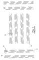
- FIG. 1schematically illustrates a top view of an existing 3-segmented alignment mark structure having both horizontally and vertically oriented alignment marks
- FIG. 2is a top view detailing one of the uniformly dimensioned, 3-segmented alignment marks shown in FIG. 1;
- FIG. 3schematically illustrates a top view of an exemplary embodiment of a novel alignment mark structure having horizontally and vertically oriented alignment marks
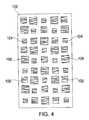
- FIG. 4is a top view detailing one of the alignment marks shown in FIG. 3, particularly illustrating a variable segmented pattern that forms the mark;
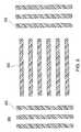
- FIG. 5schematically illustrates a top view of an alternative embodiment of the alignment mark structure of FIG. 3.
- FIG. 6is a top view detailing one of the alignment marks shown in FIG. 5, particularly illustrating an alternative segmented pattern that forms the mark.
- the alignment mark structure 10is a Nikon “2DFIA” 3-segmented mark including a series of alignment marks 12 arranged in horizontal and vertical patterns.
- Each alignment mark 12is further broken down into three individual segments 14 , as can be see in greater detail in FIG. 2.
- the segments 14are generally of a uniform length and width and may be formed upon a particular layer of a semiconductor wafer during the manufacturing process thereof.
- the segments 14may also take the form of raised surfaces upon a layer or, alternatively, trenches formed within the layer.
- the segments 14are shown in closer detail in FIG. 2.
- the segment configuration in conventional alignment mark arrangementsis that of a fairly uniform layout.
- the segmentationis designed such that process characteristics such as polish and metal fill create a clear mark of high contrast.
- variations or changes in the processcan render the mark less useful if the segmentation dimension used in the mark is specifically impacted in some way by the process change.
- the alignment markswill still show up in clear contrast if there is a process change or variation in the dimension of the segmentation. As such, if part of a process results in a failure to delineate one dimension of segmentation within the mark, another dimension of segmentation should still appear in good contrast instead.
- the desired periodicities read by a stepperwill still be retained, however the individual features making up the segmentation are varied in size and/or shape such that at least some part of the mark will appear in good contrast after processing.
- FIG. 3there is shown a top view of a 3-segmented alignment mark structure 100 , in accordance with an embodiment of the invention.
- the individual marks 102are shown in the same general configuration of those in FIG. 1 (i.e., the Nikon 2DFIA configuration of rows of horizontally and vertically disposed marks). It will be come readily apparent, however, upon closer inspection of the make up of the individual marks, that the patterning thereof provides a robust pattern of contrast notwithstanding any process changes or variations.
- each individual mark 102is formed from a pattern of squares having various ranges of sub-micron sizes.
- the squaresmay be formed as either raised surfaces or depressions within the wafer, they are illustrated herein as being depressions or holes formed in the wafer surface.
- the pattern of squaresis shown in greater detail in FIG. 4.
- the squaresare further arranged into an array of rows and columns wherein any given square in the array is directly adjacent another square of a different size in a horizontal or vertical direction.
- a square of (for example) the first sizeis only proximate another square of the first size in a diagonal direction.
- an exemplary size range for the squaresmay be 0.5, 0.6 and 0.8 microns ( ⁇ m) for the side lengths of three square sizes, respectively. However, for certain other processes, the range may be increased or decreased (e.g., 0.15, 0.20 and 0.25 ⁇ m).
- the patterning of the squaresneed not be limited to just three discrete sizes, nor need the squares be arranged in a row/column fashion. Rather, the significance of the illustrated embodiment lies in the variation of the dimension of the alignment mark segmentation.
- the marksmay be made to be visible with good contrast under a wider range of process conditions that may be present during wafer manufacturing.
- three differently mark patternsit is anticipated that at least one-third of the marks will be detected regardless of any encountered process variations.
- the increased contrast and better alignment for wafers and lots within a processresults in a decreased cost of rework processes and the possible redesign of new, customized alignment marks and the manufacture of new reticles to create such new marks.
- FIGS. 5 and 6illustrate one possible alternative embodiment for an alignment mark structure 200 .
- a Nikon 2DFIA mark structureis shown in FIG. 5.
- the basic unit which makes up an individual mark 202is an elongated diagonal that may take the form of a diagonally disposed trench or, alternatively, a diagonally disposed ridge.
- the elongated diagonalsare formed with three distinct widths 204 , 206 , 208 to provide good contrast.
- each diagonalis bordered by at least one other diagonal having a different width.
- the exemplary base patterns shown and described hereinthus far have all been regular patterns and of the same feature shape, it will further be appreciated that it is also within the scope of the present invention to have different feature shapes mixed in the same base pattern (as well as to have irregular patterns), so long as the pattern continues throughout the entire length of the segment.
- the base patterncould include both rectangles and diagonals.
Landscapes
- Physics & Mathematics (AREA)
- Condensed Matter Physics & Semiconductors (AREA)
- General Physics & Mathematics (AREA)
- Engineering & Computer Science (AREA)
- Computer Hardware Design (AREA)
- Microelectronics & Electronic Packaging (AREA)
- Power Engineering (AREA)
- Exposure And Positioning Against Photoresist Photosensitive Materials (AREA)
- Exposure Of Semiconductors, Excluding Electron Or Ion Beam Exposure (AREA)
Abstract
Description
- The present disclosure relates generally to semiconductor device manufacturing and, more particularly, to a process-robust alignment mark structure for semiconductor wafers.[0001]
- The fabrication of integrated circuit (IC) devices on a semiconductor wafer involves a number of steps wherein patterns are transferred from photolithographic masks to the wafer. A masking step, for example, includes an etching step and defines selected areas to be exposed on the wafer for subsequent processes such as oxidation, metal deposition and impurity introduction. With IC device and feature sizes becoming increasingly smaller, it is important for a photolithographic mask to be aligned precisely with the wafer during the masking step in order to minimize any misalignment between the layers.[0002]
- Most alignment schemes utilize alignment targets or marks that are defined on the wafer during a previous processing step. Typically, each alignment target includes topographical marks which may be formed by etching a plurality of “steps” into the wafer. These steps may have, for example, a height of about 1,200 angstroms (Å), with a width and spacing therebetween of about 10 microns (μm). The alignment targets are used to diffract a laser alignment beam generated by a photolithography machine (commonly known as a wafer stepper) during the masking process. The diffraction pattern is received by the wafer stepper, and the relative position of the wafer and the photolithographic mask is thereafter adjusted accordingly so that the pattern of the photolithographic mask is transferred to the wafer in the precise location as desired.[0003]
- Alignment marks created on wafer layers are often specifically designed with the particular processing step in mind in order to result in a sufficient contrast with the processed layer. For example, during the fabrication of the integrated circuit structures, a number of metallization layers are formed. Each of the metallization layers is typically separated from another metallization layer by an insulating layer therebetween. To provide an overlying metallization layer without discontinuities or other flaws, it is desirous to have an underlying surface for the metallization layer that is as flat or planar as possible. It has thus become commonplace to smooth the surface of a layer in preparation for a subsequently formed metallization layer by applying a planarization process. Certain planarization techniques, such as chemical-mechanical polishing (CMP), often result in a dishing or indentation of the wafer surface. Accordingly, alignment marks to be formed in metallization layers may include small segmented patterns of a uniform dimension so that dishing does not affect the integrity of the mark. A particular segment dimension may even be determined experimentally or by trial and error prior to incorporating the mark design into the wafer.[0004]
- Unfortunately, process variations can also impact the contrast of an alignment mark. For example, a variation in the degree of CMP dishing, or perhaps a variation in the amount of applied chemical vapor deposition (CVD) metal fill, might make a mark more or less visible with regard to the particular imaging method of the wafer stepper. The variations may be from wafer to wafer and lot to lot. Furthermore, a change in process can result in the necessity for new alignment mark design and/or new reticle manufacture, along with the increased costs associated therewith. It is desirable, therefore, to provide an alignment mark structure with reduced susceptibility to process variability which might otherwise result in rework or other adverse effects upon the IC chip function.[0005]
- The above discussed and other drawbacks and deficiencies of the prior art are overcome or alleviated by an alignment mark structure for use upon a semiconductor substrate. In an exemplary embodiment, the alignment mark structure includes a plurality of segments arranged in an alignment pattern, with each of the plurality of segments being formed from a base pattern created on the substrate. The base pattern includes a plurality of sizes, wherein each of the plurality of sizes of the base pattern is repeated throughout an entire length of each of the plurality of segments.[0006]
- In one aspect, the base pattern is a square pattern wherein individual squares within the base pattern are arranged into rows and columns, with each square being situated proximate another square having a different size, along a horizontal and vertical direction. The individual squares may be formed as raised surfaces on the semiconductor substrate or, alternatively, as depressions within the semiconductor substrate. In an alternative embodiment, the base pattern is an elongated diagonal.[0007]
- Referring to the exemplary drawings wherein like elements are numbered alike in the several Figures:[0008]
- FIG. 1 schematically illustrates a top view of an existing 3-segmented alignment mark structure having both horizontally and vertically oriented alignment marks;[0009]
- FIG. 2 is a top view detailing one of the uniformly dimensioned, 3-segmented alignment marks shown in FIG. 1;[0010]
- FIG. 3 schematically illustrates a top view of an exemplary embodiment of a novel alignment mark structure having horizontally and vertically oriented alignment marks;[0011]
- FIG. 4 is a top view detailing one of the alignment marks shown in FIG. 3, particularly illustrating a variable segmented pattern that forms the mark;[0012]
- FIG. 5 schematically illustrates a top view of an alternative embodiment of the alignment mark structure of FIG. 3; and[0013]
- FIG. 6 is a top view detailing one of the alignment marks shown in FIG. 5, particularly illustrating an alternative segmented pattern that forms the mark.[0014]
- Referring initially to FIG. 1, there is shown a top view of an existing 3-segmented[0015]
alignment mark structure 10. In the example shown, thealignment mark structure 10 is a Nikon “2DFIA” 3-segmented mark including a series ofalignment marks 12 arranged in horizontal and vertical patterns. Eachalignment mark 12 is further broken down into threeindividual segments 14, as can be see in greater detail in FIG. 2. Thesegments 14 are generally of a uniform length and width and may be formed upon a particular layer of a semiconductor wafer during the manufacturing process thereof. Thesegments 14 may also take the form of raised surfaces upon a layer or, alternatively, trenches formed within the layer. - The[0016]
segments 14 are shown in closer detail in FIG. 2. As can be seen, the segment configuration in conventional alignment mark arrangements is that of a fairly uniform layout. Ideally, the segmentation is designed such that process characteristics such as polish and metal fill create a clear mark of high contrast. However, as stated previously, variations or changes in the process can render the mark less useful if the segmentation dimension used in the mark is specifically impacted in some way by the process change. - Therefore, in accordance with an embodiment of the invention, there is disclosed a novel alignment mark structure and method that is robust to process changes or variations. That is, the alignment marks will still show up in clear contrast if there is a process change or variation in the dimension of the segmentation. As such, if part of a process results in a failure to delineate one dimension of segmentation within the mark, another dimension of segmentation should still appear in good contrast instead. Generally stated, the desired periodicities read by a stepper will still be retained, however the individual features making up the segmentation are varied in size and/or shape such that at least some part of the mark will appear in good contrast after processing.[0017]
- Referring now to FIG. 3, there is shown a top view of a 3-segmented[0018]
alignment mark structure 100, in accordance with an embodiment of the invention. For purposes of comparison only, theindividual marks 102 are shown in the same general configuration of those in FIG. 1 (i.e., the Nikon 2DFIA configuration of rows of horizontally and vertically disposed marks). It will be come readily apparent, however, upon closer inspection of the make up of the individual marks, that the patterning thereof provides a robust pattern of contrast notwithstanding any process changes or variations. - In the embodiment depicted in FIG. 3, each[0019]
individual mark 102 is formed from a pattern of squares having various ranges of sub-micron sizes. Although the squares may be formed as either raised surfaces or depressions within the wafer, they are illustrated herein as being depressions or holes formed in the wafer surface. The pattern of squares is shown in greater detail in FIG. 4. As is shown, there are three individual square sizes, represented bysquares 104 having a first size,squares 106 having a second size greater than the first size, and bysquares 108 having a third size greater than the second size. In an exemplary embodiment, the squares are further arranged into an array of rows and columns wherein any given square in the array is directly adjacent another square of a different size in a horizontal or vertical direction. In other words, a square of (for example) the first size is only proximate another square of the first size in a diagonal direction. Depending upon the particular manufacturing process, an exemplary size range for the squares may be 0.5, 0.6 and 0.8 microns (μm) for the side lengths of three square sizes, respectively. However, for certain other processes, the range may be increased or decreased (e.g., 0.15, 0.20 and 0.25 μm). - It will be appreciated that the patterning of the squares need not be limited to just three discrete sizes, nor need the squares be arranged in a row/column fashion. Rather, the significance of the illustrated embodiment lies in the variation of the dimension of the alignment mark segmentation. Thus configured, the marks may be made to be visible with good contrast under a wider range of process conditions that may be present during wafer manufacturing. By having, for example, three differently mark patterns, it is anticipated that at least one-third of the marks will be detected regardless of any encountered process variations. In turn, the increased contrast and better alignment for wafers and lots within a process results in a decreased cost of rework processes and the possible redesign of new, customized alignment marks and the manufacture of new reticles to create such new marks.[0020]
- Not only are the size and arrangement of the square marks not limited to the example of FIG. 4, other base shapes may also be used. For example, FIGS. 5 and 6 illustrate one possible alternative embodiment for an[0021]
alignment mark structure 200. Again, for purposes of comparison, a Nikon 2DFIA mark structure is shown in FIG. 5. As is shown most particularly in FIG. 6, the basic unit which makes up anindividual mark 202 is an elongated diagonal that may take the form of a diagonally disposed trench or, alternatively, a diagonally disposed ridge. Like the embodiment of FIGS. 3 and 4, the elongated diagonals are formed with threedistinct widths - Moreover, although the exemplary base patterns shown and described herein thus far have all been regular patterns and of the same feature shape, it will further be appreciated that it is also within the scope of the present invention to have different feature shapes mixed in the same base pattern (as well as to have irregular patterns), so long as the pattern continues throughout the entire length of the segment. For example, the base pattern could include both rectangles and diagonals.[0022]
- While the invention has been described with reference to a preferred embodiment, it will be understood by those skilled in the art that various changes may be made and equivalents may be substituted for elements thereof without departing from the scope of the invention. In addition, many modifications may be made to adapt a particular situation or material to the teachings of the invention without departing from the essential scope thereof. Therefore, it is intended that the invention not be limited to the particular embodiment disclosed as the best mode contemplated for carrying out this invention, but that the invention will include all embodiments falling within the scope of the appended claims.[0023]
Claims (20)
Priority Applications (1)
| Application Number | Priority Date | Filing Date | Title |
|---|---|---|---|
| US10/303,501US6803668B2 (en) | 2002-11-22 | 2002-11-22 | Process-robust alignment mark structure for semiconductor wafers |
Applications Claiming Priority (1)
| Application Number | Priority Date | Filing Date | Title |
|---|---|---|---|
| US10/303,501US6803668B2 (en) | 2002-11-22 | 2002-11-22 | Process-robust alignment mark structure for semiconductor wafers |
Publications (2)
| Publication Number | Publication Date |
|---|---|
| US20040099963A1true US20040099963A1 (en) | 2004-05-27 |
| US6803668B2 US6803668B2 (en) | 2004-10-12 |
Family
ID=32325018
Family Applications (1)
| Application Number | Title | Priority Date | Filing Date |
|---|---|---|---|
| US10/303,501Expired - Fee RelatedUS6803668B2 (en) | 2002-11-22 | 2002-11-22 | Process-robust alignment mark structure for semiconductor wafers |
Country Status (1)
| Country | Link |
|---|---|
| US (1) | US6803668B2 (en) |
Cited By (9)
| Publication number | Priority date | Publication date | Assignee | Title |
|---|---|---|---|---|
| US20030020184A1 (en)* | 2001-05-23 | 2003-01-30 | Ballarin Eugenio Guido | Substrate provided with an alignment mark, method of designing a mask, computer program, mask for exposing said mark, device manufacturing method, and device manufactured thereby |
| US20050091863A1 (en)* | 2003-11-04 | 2005-05-05 | Taiwan Semiconductor Manufacturing Co. Ltd. | Calibration wafer and kit |
| US20050096779A1 (en)* | 2003-10-30 | 2005-05-05 | Asml Holding N.V. | Tunable alignment geometry |
| US20070052114A1 (en)* | 2005-09-07 | 2007-03-08 | Shih-Chieh Huang | Alignment checking structure and process using thereof |
| US20070069400A1 (en)* | 2001-09-17 | 2007-03-29 | Canon Kabushiki Kaisha | Alignment mark, alignment apparatus and method, exposure apparatus, and device manufacturing method |
| US20100134513A1 (en)* | 2008-12-03 | 2010-06-03 | Panasonic Corporation | Pixel display device |
| US20110101546A1 (en)* | 2007-09-10 | 2011-05-05 | Stats Chippac, Ltd. | System and Method for Directional Grinding on Backside of a Semiconductor Wafer |
| KR20200123486A (en)* | 2012-11-21 | 2020-10-29 | 케이엘에이 코포레이션 | Process compatible segmented targets and design methods |
| US20210193493A1 (en)* | 2019-12-18 | 2021-06-24 | Micron Technology, Inc. | Wafer overlay marks, overlay measurement systems, and related methods |
Families Citing this family (7)
| Publication number | Priority date | Publication date | Assignee | Title |
|---|---|---|---|---|
| JP4007231B2 (en)* | 2003-04-01 | 2007-11-14 | ソニー株式会社 | Mark detection method and exposure method |
| TW200507228A (en)* | 2003-04-08 | 2005-02-16 | Aoti Operating Co Inc | Overlay metrology mark |
| US7435659B2 (en)* | 2005-02-28 | 2008-10-14 | Texas Instruments Incorporated | Method for manufacturing a semiconductor device having an alignment feature formed using an N-type dopant and a wet oxidation process |
| US7687925B2 (en)* | 2005-09-07 | 2010-03-30 | Infineon Technologies Ag | Alignment marks for polarized light lithography and method for use thereof |
| US7532305B2 (en)* | 2006-03-28 | 2009-05-12 | Asml Netherlands B.V. | Lithographic apparatus and device manufacturing method using overlay measurement |
| US10199330B2 (en) | 2013-12-23 | 2019-02-05 | Infineon Technologies Ag | Alignment mark arrangement, semiconductor workpiece, and method for aligning a wafer |
| US11239086B2 (en) | 2018-05-14 | 2022-02-01 | Applied Materials, Inc. | Back end memory integration process |
Family Cites Families (15)
| Publication number | Priority date | Publication date | Assignee | Title |
|---|---|---|---|---|
| US4704027A (en) | 1986-06-19 | 1987-11-03 | Compact Spindle Bearing Corporation | Dark field alignment and alignment mark systems |
| US5329334A (en) | 1993-03-02 | 1994-07-12 | Lsi Logic Corporation | Integrated circuit test reticle and alignment mark optimization method |
| US5503962A (en) | 1994-07-15 | 1996-04-02 | Cypress Semiconductor Corporation | Chemical-mechanical alignment mark and method of fabrication |
| US5786260A (en) | 1996-12-16 | 1998-07-28 | Taiwan Semiconductor Manufacturing Company, Ltd. | Method of fabricating a readable alignment mark structure using enhanced chemical mechanical polishing |
| US5911108A (en) | 1997-01-29 | 1999-06-08 | Integrated Device Technology, Inc. | Method for protecting an alignment mark on a semiconductor substrate during chemical mechanical polishing and the resulting structure |
| US5923996A (en) | 1997-06-02 | 1999-07-13 | Taiwan Semiconductor Manufacturing Company, Ltd | Method to protect alignment mark in CMP process |
| US5952241A (en)* | 1997-09-03 | 1999-09-14 | Vlsi Technology, Inc. | Method and apparatus for improving alignment for metal masking in conjuction with oxide and tungsten CMP |
| US5981352A (en) | 1997-09-08 | 1999-11-09 | Lsi Logic Corporation | Consistent alignment mark profiles on semiconductor wafers using fine grain tungsten protective layer |
| US6249036B1 (en) | 1998-03-18 | 2001-06-19 | Advanced Micro Devices, Inc. | Stepper alignment mark formation with dual field oxide process |
| US6022649A (en) | 1998-09-21 | 2000-02-08 | Chartered Semiconductor Manufacturing, Ltd. | Wafer stepper method utilizing a multi-segment global alignment mark |
| JP4132298B2 (en)* | 1998-10-27 | 2008-08-13 | 株式会社ルネサステクノロジ | Semiconductor device having overlay inspection mark |
| US6037671A (en) | 1998-11-03 | 2000-03-14 | Advanced Micro Devices, Inc. | Stepper alignment mark structure for maintaining alignment integrity |
| TW388803B (en)* | 1999-03-29 | 2000-05-01 | Nanya Technology Corp | A structure and method of measuring overlapping marks |
| US6342735B1 (en)* | 1999-09-01 | 2002-01-29 | International Business Machines Corporation | Dual use alignment aid |
| JP4038320B2 (en)* | 2000-04-17 | 2008-01-23 | 株式会社東芝 | Semiconductor integrated device |
- 2002
- 2002-11-22USUS10/303,501patent/US6803668B2/ennot_activeExpired - Fee Related
Cited By (21)
| Publication number | Priority date | Publication date | Assignee | Title |
|---|---|---|---|---|
| US7560196B2 (en) | 2001-05-23 | 2009-07-14 | Asml Netherlands B.V. | Mask for exposing an alignment mark, and method and computer program for designing the mask |
| US6876092B2 (en)* | 2001-05-23 | 2005-04-05 | Asml Netherlands B.V. | Substrate provided with an alignment mark, method of designing a mask, computer program, mask for exposing said mark, device manufacturing method, and device manufactured thereby |
| US20050084772A1 (en)* | 2001-05-23 | 2005-04-21 | Asml Netherlands B.V. | Mask for exposing an alignment mark, and method and computer program for designing the mask |
| US20030020184A1 (en)* | 2001-05-23 | 2003-01-30 | Ballarin Eugenio Guido | Substrate provided with an alignment mark, method of designing a mask, computer program, mask for exposing said mark, device manufacturing method, and device manufactured thereby |
| US20070069400A1 (en)* | 2001-09-17 | 2007-03-29 | Canon Kabushiki Kaisha | Alignment mark, alignment apparatus and method, exposure apparatus, and device manufacturing method |
| US7838310B2 (en) | 2003-10-30 | 2010-11-23 | Asml Holding N.V. | Tunable alignment geometry |
| US20050096779A1 (en)* | 2003-10-30 | 2005-05-05 | Asml Holding N.V. | Tunable alignment geometry |
| US7112890B2 (en)* | 2003-10-30 | 2006-09-26 | Asml Holding N.V. | Tunable alignment geometry |
| US20070004053A1 (en)* | 2003-10-30 | 2007-01-04 | Asml Holding N.V. | Tunable alignment geometry |
| US20090201505A1 (en)* | 2003-10-30 | 2009-08-13 | Asml Holding N.V. | Tunable Alignment Geometry |
| US7534637B2 (en) | 2003-10-30 | 2009-05-19 | Asml Holding N.V. | Tunable alignment geometry |
| US6914337B2 (en)* | 2003-11-04 | 2005-07-05 | Taiwan Semiconductor Manufacturing Co., Ltd | Calibration wafer and kit |
| US20050091863A1 (en)* | 2003-11-04 | 2005-05-05 | Taiwan Semiconductor Manufacturing Co. Ltd. | Calibration wafer and kit |
| US20070052114A1 (en)* | 2005-09-07 | 2007-03-08 | Shih-Chieh Huang | Alignment checking structure and process using thereof |
| US20110101546A1 (en)* | 2007-09-10 | 2011-05-05 | Stats Chippac, Ltd. | System and Method for Directional Grinding on Backside of a Semiconductor Wafer |
| US8994196B2 (en)* | 2007-09-10 | 2015-03-31 | Stats Chippac, Ltd. | System and method for directional grinding on backside of a semiconductor wafer |
| US20100134513A1 (en)* | 2008-12-03 | 2010-06-03 | Panasonic Corporation | Pixel display device |
| KR20200123486A (en)* | 2012-11-21 | 2020-10-29 | 케이엘에이 코포레이션 | Process compatible segmented targets and design methods |
| KR102312241B1 (en) | 2012-11-21 | 2021-10-13 | 케이엘에이 코포레이션 | Process compatible segmented targets and design methods |
| US20210193493A1 (en)* | 2019-12-18 | 2021-06-24 | Micron Technology, Inc. | Wafer overlay marks, overlay measurement systems, and related methods |
| US11784077B2 (en)* | 2019-12-18 | 2023-10-10 | Micron Technology, Inc. | Wafer overlay marks, overlay measurement systems, and related methods |
Also Published As
| Publication number | Publication date |
|---|---|
| US6803668B2 (en) | 2004-10-12 |
Similar Documents
| Publication | Publication Date | Title |
|---|---|---|
| US6803668B2 (en) | Process-robust alignment mark structure for semiconductor wafers | |
| US10504846B2 (en) | Semiconductor device | |
| US5786267A (en) | Method of making a semiconductor wafer with alignment marks | |
| US6261918B1 (en) | Method for creating and preserving alignment marks for aligning mask layers in integrated circuit manufacture | |
| US6172409B1 (en) | Buffer grated structure for metrology mark and method for making the same | |
| US6645823B2 (en) | Reticle and method of fabricating semiconductor device | |
| US5982044A (en) | Alignment pattern and algorithm for photolithographic alignment marks on semiconductor substrates | |
| JP3556647B2 (en) | Method for manufacturing semiconductor device | |
| US12009212B2 (en) | Semiconductor device with reduced critical dimensions | |
| US6146969A (en) | Printing optimized global alignment mark at contact/via layers | |
| US6271602B1 (en) | Method for reducing the susceptibility to chemical-mechanical polishing damage of an alignment mark formed in a semiconductor substrate | |
| US6498401B2 (en) | Alignment mark set and method of measuring alignment accuracy | |
| US7160656B2 (en) | Method for determining pattern misalignment over a substrate | |
| US6822342B2 (en) | Raised-lines overlay semiconductor targets and method of making the same | |
| US6340631B1 (en) | Method for laying out wide metal lines with embedded contacts/vias | |
| US20020179941A1 (en) | Semiconductor device and method of manufacturing the same | |
| TWI817438B (en) | Overlay mark | |
| US20090311865A1 (en) | Method for double patterning lithography | |
| KR100661728B1 (en) | Dummy Layer of Semiconductor Device | |
| EP0631316A2 (en) | Semiconductor device comprising an alignment mark, method of manufacturing the same and aligning method | |
| JP3698843B2 (en) | Photo mask | |
| JP2762500B2 (en) | Semiconductor device | |
| KR20060027315A (en) | Method and apparatus for manufacturing diamond shaped chip | |
| CN116960110A (en) | Overlay mark | |
| KR20050039455A (en) | Semiconductor device having integrated alignment key formed in edge region of a wafer and method for manufacturing the same |
Legal Events
| Date | Code | Title | Description |
|---|---|---|---|
| AS | Assignment | Owner name:INTERNATIONAL BUSINESS MACHINES CORPORATION, NEW Y Free format text:ASSIGNMENT OF ASSIGNORS INTEREST;ASSIGNORS:HOLLOWAY, KAREN L.;LU, ANDREW;WU, QIANG;REEL/FRAME:013547/0025;SIGNING DATES FROM 20021107 TO 20021121 | |
| FEPP | Fee payment procedure | Free format text:PAYOR NUMBER ASSIGNED (ORIGINAL EVENT CODE: ASPN); ENTITY STATUS OF PATENT OWNER: LARGE ENTITY | |
| FPAY | Fee payment | Year of fee payment:4 | |
| REMI | Maintenance fee reminder mailed | ||
| FPAY | Fee payment | Year of fee payment:8 | |
| SULP | Surcharge for late payment | Year of fee payment:7 | |
| AS | Assignment | Owner name:GLOBALFOUNDRIES U.S. 2 LLC, NEW YORK Free format text:ASSIGNMENT OF ASSIGNORS INTEREST;ASSIGNOR:INTERNATIONAL BUSINESS MACHINES CORPORATION;REEL/FRAME:036550/0001 Effective date:20150629 | |
| AS | Assignment | Owner name:GLOBALFOUNDRIES INC., CAYMAN ISLANDS Free format text:ASSIGNMENT OF ASSIGNORS INTEREST;ASSIGNORS:GLOBALFOUNDRIES U.S. 2 LLC;GLOBALFOUNDRIES U.S. INC.;REEL/FRAME:036779/0001 Effective date:20150910 | |
| REMI | Maintenance fee reminder mailed | ||
| LAPS | Lapse for failure to pay maintenance fees | ||
| STCH | Information on status: patent discontinuation | Free format text:PATENT EXPIRED DUE TO NONPAYMENT OF MAINTENANCE FEES UNDER 37 CFR 1.362 | |
| FP | Lapsed due to failure to pay maintenance fee | Effective date:20161012 | |
| AS | Assignment | Owner name:GLOBALFOUNDRIES U.S. INC., NEW YORK Free format text:RELEASE BY SECURED PARTY;ASSIGNOR:WILMINGTON TRUST, NATIONAL ASSOCIATION;REEL/FRAME:056987/0001 Effective date:20201117 |