US20040097030A1 - Semiconductor device including gate electrode for applying tensile stress to silicon substrate, and method of manufacturing the same - Google Patents
Semiconductor device including gate electrode for applying tensile stress to silicon substrate, and method of manufacturing the sameDownload PDFInfo
- Publication number
- US20040097030A1 US20040097030A1US10/620,379US62037903AUS2004097030A1US 20040097030 A1US20040097030 A1US 20040097030A1US 62037903 AUS62037903 AUS 62037903AUS 2004097030 A1US2004097030 A1US 2004097030A1
- Authority
- US
- United States
- Prior art keywords
- gate electrode
- ions
- silicon substrate
- semiconductor device
- gate
- Prior art date
- Legal status (The legal status is an assumption and is not a legal conclusion. Google has not performed a legal analysis and makes no representation as to the accuracy of the status listed.)
- Granted
Links
Images


Classifications
- H—ELECTRICITY
- H10—SEMICONDUCTOR DEVICES; ELECTRIC SOLID-STATE DEVICES NOT OTHERWISE PROVIDED FOR
- H10D—INORGANIC ELECTRIC SEMICONDUCTOR DEVICES
- H10D30/00—Field-effect transistors [FET]
- H10D30/60—Insulated-gate field-effect transistors [IGFET]
- H—ELECTRICITY
- H01—ELECTRIC ELEMENTS
- H01L—SEMICONDUCTOR DEVICES NOT COVERED BY CLASS H10
- H01L21/00—Processes or apparatus adapted for the manufacture or treatment of semiconductor or solid state devices or of parts thereof
- H01L21/02—Manufacture or treatment of semiconductor devices or of parts thereof
- H01L21/04—Manufacture or treatment of semiconductor devices or of parts thereof the devices having potential barriers, e.g. a PN junction, depletion layer or carrier concentration layer
- H01L21/18—Manufacture or treatment of semiconductor devices or of parts thereof the devices having potential barriers, e.g. a PN junction, depletion layer or carrier concentration layer the devices having semiconductor bodies comprising elements of Group IV of the Periodic Table or AIIIBV compounds with or without impurities, e.g. doping materials
- H01L21/26—Bombardment with radiation
- H01L21/263—Bombardment with radiation with high-energy radiation
- H01L21/265—Bombardment with radiation with high-energy radiation producing ion implantation
- H01L21/26506—Bombardment with radiation with high-energy radiation producing ion implantation in group IV semiconductors
- H—ELECTRICITY
- H01—ELECTRIC ELEMENTS
- H01L—SEMICONDUCTOR DEVICES NOT COVERED BY CLASS H10
- H01L21/00—Processes or apparatus adapted for the manufacture or treatment of semiconductor or solid state devices or of parts thereof
- H01L21/02—Manufacture or treatment of semiconductor devices or of parts thereof
- H01L21/04—Manufacture or treatment of semiconductor devices or of parts thereof the devices having potential barriers, e.g. a PN junction, depletion layer or carrier concentration layer
- H01L21/18—Manufacture or treatment of semiconductor devices or of parts thereof the devices having potential barriers, e.g. a PN junction, depletion layer or carrier concentration layer the devices having semiconductor bodies comprising elements of Group IV of the Periodic Table or AIIIBV compounds with or without impurities, e.g. doping materials
- H01L21/30—Treatment of semiconductor bodies using processes or apparatus not provided for in groups H01L21/20 - H01L21/26
- H01L21/31—Treatment of semiconductor bodies using processes or apparatus not provided for in groups H01L21/20 - H01L21/26 to form insulating layers thereon, e.g. for masking or by using photolithographic techniques; After treatment of these layers; Selection of materials for these layers
- H01L21/3205—Deposition of non-insulating-, e.g. conductive- or resistive-, layers on insulating layers; After-treatment of these layers
- H01L21/321—After treatment
- H01L21/3215—Doping the layers
- H01L21/32155—Doping polycristalline - or amorphous silicon layers
- H—ELECTRICITY
- H10—SEMICONDUCTOR DEVICES; ELECTRIC SOLID-STATE DEVICES NOT OTHERWISE PROVIDED FOR
- H10B—ELECTRONIC MEMORY DEVICES
- H10B10/00—Static random access memory [SRAM] devices
- H10B10/12—Static random access memory [SRAM] devices comprising a MOSFET load element
- H—ELECTRICITY
- H10—SEMICONDUCTOR DEVICES; ELECTRIC SOLID-STATE DEVICES NOT OTHERWISE PROVIDED FOR
- H10B—ELECTRONIC MEMORY DEVICES
- H10B10/00—Static random access memory [SRAM] devices
- H10B10/18—Peripheral circuit regions
- H—ELECTRICITY
- H10—SEMICONDUCTOR DEVICES; ELECTRIC SOLID-STATE DEVICES NOT OTHERWISE PROVIDED FOR
- H10B—ELECTRONIC MEMORY DEVICES
- H10B12/00—Dynamic random access memory [DRAM] devices
- H10B12/01—Manufacture or treatment
- H—ELECTRICITY
- H10—SEMICONDUCTOR DEVICES; ELECTRIC SOLID-STATE DEVICES NOT OTHERWISE PROVIDED FOR
- H10B—ELECTRONIC MEMORY DEVICES
- H10B12/00—Dynamic random access memory [DRAM] devices
- H10B12/01—Manufacture or treatment
- H10B12/09—Manufacture or treatment with simultaneous manufacture of the peripheral circuit region and memory cells
- H—ELECTRICITY
- H10—SEMICONDUCTOR DEVICES; ELECTRIC SOLID-STATE DEVICES NOT OTHERWISE PROVIDED FOR
- H10B—ELECTRONIC MEMORY DEVICES
- H10B12/00—Dynamic random access memory [DRAM] devices
- H10B12/30—DRAM devices comprising one-transistor - one-capacitor [1T-1C] memory cells
- H—ELECTRICITY
- H10—SEMICONDUCTOR DEVICES; ELECTRIC SOLID-STATE DEVICES NOT OTHERWISE PROVIDED FOR
- H10B—ELECTRONIC MEMORY DEVICES
- H10B12/00—Dynamic random access memory [DRAM] devices
- H10B12/50—Peripheral circuit region structures
- H—ELECTRICITY
- H10—SEMICONDUCTOR DEVICES; ELECTRIC SOLID-STATE DEVICES NOT OTHERWISE PROVIDED FOR
- H10D—INORGANIC ELECTRIC SEMICONDUCTOR DEVICES
- H10D30/00—Field-effect transistors [FET]
- H10D30/01—Manufacture or treatment
- H10D30/021—Manufacture or treatment of FETs having insulated gates [IGFET]
- H—ELECTRICITY
- H10—SEMICONDUCTOR DEVICES; ELECTRIC SOLID-STATE DEVICES NOT OTHERWISE PROVIDED FOR
- H10D—INORGANIC ELECTRIC SEMICONDUCTOR DEVICES
- H10D30/00—Field-effect transistors [FET]
- H10D30/60—Insulated-gate field-effect transistors [IGFET]
- H10D30/791—Arrangements for exerting mechanical stress on the crystal lattice of the channel regions
- H10D30/794—Arrangements for exerting mechanical stress on the crystal lattice of the channel regions comprising conductive materials, e.g. silicided source, drain or gate electrodes
- H—ELECTRICITY
- H10—SEMICONDUCTOR DEVICES; ELECTRIC SOLID-STATE DEVICES NOT OTHERWISE PROVIDED FOR
- H10D—INORGANIC ELECTRIC SEMICONDUCTOR DEVICES
- H10D30/00—Field-effect transistors [FET]
- H10D30/60—Insulated-gate field-effect transistors [IGFET]
- H10D30/791—Arrangements for exerting mechanical stress on the crystal lattice of the channel regions
- H10D30/797—Arrangements for exerting mechanical stress on the crystal lattice of the channel regions being in source or drain regions, e.g. SiGe source or drain
- H—ELECTRICITY
- H10—SEMICONDUCTOR DEVICES; ELECTRIC SOLID-STATE DEVICES NOT OTHERWISE PROVIDED FOR
- H10D—INORGANIC ELECTRIC SEMICONDUCTOR DEVICES
- H10D64/00—Electrodes of devices having potential barriers
- H10D64/60—Electrodes characterised by their materials
- H10D64/66—Electrodes having a conductor capacitively coupled to a semiconductor by an insulator, e.g. MIS electrodes
- H10D64/661—Electrodes having a conductor capacitively coupled to a semiconductor by an insulator, e.g. MIS electrodes the conductor comprising a layer of silicon contacting the insulator, e.g. polysilicon having vertical doping variation
- H10D64/662—Electrodes having a conductor capacitively coupled to a semiconductor by an insulator, e.g. MIS electrodes the conductor comprising a layer of silicon contacting the insulator, e.g. polysilicon having vertical doping variation the conductor further comprising additional layers, e.g. multiple silicon layers having different crystal structures
- H10D64/663—Electrodes having a conductor capacitively coupled to a semiconductor by an insulator, e.g. MIS electrodes the conductor comprising a layer of silicon contacting the insulator, e.g. polysilicon having vertical doping variation the conductor further comprising additional layers, e.g. multiple silicon layers having different crystal structures the additional layers comprising a silicide layer contacting the layer of silicon, e.g. polycide gates
- H—ELECTRICITY
- H10—SEMICONDUCTOR DEVICES; ELECTRIC SOLID-STATE DEVICES NOT OTHERWISE PROVIDED FOR
- H10D—INORGANIC ELECTRIC SEMICONDUCTOR DEVICES
- H10D84/00—Integrated devices formed in or on semiconductor substrates that comprise only semiconducting layers, e.g. on Si wafers or on GaAs-on-Si wafers
- H10D84/01—Manufacture or treatment
- H10D84/0123—Integrating together multiple components covered by H10D12/00 or H10D30/00, e.g. integrating multiple IGBTs
- H10D84/0126—Integrating together multiple components covered by H10D12/00 or H10D30/00, e.g. integrating multiple IGBTs the components including insulated gates, e.g. IGFETs
- H10D84/0128—Manufacturing their channels
- H—ELECTRICITY
- H10—SEMICONDUCTOR DEVICES; ELECTRIC SOLID-STATE DEVICES NOT OTHERWISE PROVIDED FOR
- H10D—INORGANIC ELECTRIC SEMICONDUCTOR DEVICES
- H10D84/00—Integrated devices formed in or on semiconductor substrates that comprise only semiconducting layers, e.g. on Si wafers or on GaAs-on-Si wafers
- H10D84/01—Manufacture or treatment
- H10D84/0123—Integrating together multiple components covered by H10D12/00 or H10D30/00, e.g. integrating multiple IGBTs
- H10D84/0126—Integrating together multiple components covered by H10D12/00 or H10D30/00, e.g. integrating multiple IGBTs the components including insulated gates, e.g. IGFETs
- H10D84/013—Manufacturing their source or drain regions, e.g. silicided source or drain regions
- H—ELECTRICITY
- H10—SEMICONDUCTOR DEVICES; ELECTRIC SOLID-STATE DEVICES NOT OTHERWISE PROVIDED FOR
- H10D—INORGANIC ELECTRIC SEMICONDUCTOR DEVICES
- H10D84/00—Integrated devices formed in or on semiconductor substrates that comprise only semiconducting layers, e.g. on Si wafers or on GaAs-on-Si wafers
- H10D84/01—Manufacture or treatment
- H10D84/0123—Integrating together multiple components covered by H10D12/00 or H10D30/00, e.g. integrating multiple IGBTs
- H10D84/0126—Integrating together multiple components covered by H10D12/00 or H10D30/00, e.g. integrating multiple IGBTs the components including insulated gates, e.g. IGFETs
- H10D84/0135—Manufacturing their gate conductors
- H10D84/0137—Manufacturing their gate conductors the gate conductors being silicided
- H—ELECTRICITY
- H10—SEMICONDUCTOR DEVICES; ELECTRIC SOLID-STATE DEVICES NOT OTHERWISE PROVIDED FOR
- H10D—INORGANIC ELECTRIC SEMICONDUCTOR DEVICES
- H10D84/00—Integrated devices formed in or on semiconductor substrates that comprise only semiconducting layers, e.g. on Si wafers or on GaAs-on-Si wafers
- H10D84/01—Manufacture or treatment
- H10D84/0123—Integrating together multiple components covered by H10D12/00 or H10D30/00, e.g. integrating multiple IGBTs
- H10D84/0126—Integrating together multiple components covered by H10D12/00 or H10D30/00, e.g. integrating multiple IGBTs the components including insulated gates, e.g. IGFETs
- H10D84/0165—Integrating together multiple components covered by H10D12/00 or H10D30/00, e.g. integrating multiple IGBTs the components including insulated gates, e.g. IGFETs the components including complementary IGFETs, e.g. CMOS devices
- H10D84/0167—Manufacturing their channels
- H—ELECTRICITY
- H10—SEMICONDUCTOR DEVICES; ELECTRIC SOLID-STATE DEVICES NOT OTHERWISE PROVIDED FOR
- H10D—INORGANIC ELECTRIC SEMICONDUCTOR DEVICES
- H10D84/00—Integrated devices formed in or on semiconductor substrates that comprise only semiconducting layers, e.g. on Si wafers or on GaAs-on-Si wafers
- H10D84/01—Manufacture or treatment
- H10D84/0123—Integrating together multiple components covered by H10D12/00 or H10D30/00, e.g. integrating multiple IGBTs
- H10D84/0126—Integrating together multiple components covered by H10D12/00 or H10D30/00, e.g. integrating multiple IGBTs the components including insulated gates, e.g. IGFETs
- H10D84/0165—Integrating together multiple components covered by H10D12/00 or H10D30/00, e.g. integrating multiple IGBTs the components including insulated gates, e.g. IGFETs the components including complementary IGFETs, e.g. CMOS devices
- H10D84/017—Manufacturing their source or drain regions, e.g. silicided source or drain regions
- H—ELECTRICITY
- H10—SEMICONDUCTOR DEVICES; ELECTRIC SOLID-STATE DEVICES NOT OTHERWISE PROVIDED FOR
- H10D—INORGANIC ELECTRIC SEMICONDUCTOR DEVICES
- H10D84/00—Integrated devices formed in or on semiconductor substrates that comprise only semiconducting layers, e.g. on Si wafers or on GaAs-on-Si wafers
- H10D84/01—Manufacture or treatment
- H10D84/0123—Integrating together multiple components covered by H10D12/00 or H10D30/00, e.g. integrating multiple IGBTs
- H10D84/0126—Integrating together multiple components covered by H10D12/00 or H10D30/00, e.g. integrating multiple IGBTs the components including insulated gates, e.g. IGFETs
- H10D84/0165—Integrating together multiple components covered by H10D12/00 or H10D30/00, e.g. integrating multiple IGBTs the components including insulated gates, e.g. IGFETs the components including complementary IGFETs, e.g. CMOS devices
- H10D84/0172—Manufacturing their gate conductors
- H10D84/0174—Manufacturing their gate conductors the gate conductors being silicided
- H—ELECTRICITY
- H10—SEMICONDUCTOR DEVICES; ELECTRIC SOLID-STATE DEVICES NOT OTHERWISE PROVIDED FOR
- H10D—INORGANIC ELECTRIC SEMICONDUCTOR DEVICES
- H10D84/00—Integrated devices formed in or on semiconductor substrates that comprise only semiconducting layers, e.g. on Si wafers or on GaAs-on-Si wafers
- H10D84/01—Manufacture or treatment
- H10D84/0123—Integrating together multiple components covered by H10D12/00 or H10D30/00, e.g. integrating multiple IGBTs
- H10D84/0126—Integrating together multiple components covered by H10D12/00 or H10D30/00, e.g. integrating multiple IGBTs the components including insulated gates, e.g. IGFETs
- H10D84/0165—Integrating together multiple components covered by H10D12/00 or H10D30/00, e.g. integrating multiple IGBTs the components including insulated gates, e.g. IGFETs the components including complementary IGFETs, e.g. CMOS devices
- H10D84/0172—Manufacturing their gate conductors
- H10D84/0177—Manufacturing their gate conductors the gate conductors having different materials or different implants
- H—ELECTRICITY
- H10—SEMICONDUCTOR DEVICES; ELECTRIC SOLID-STATE DEVICES NOT OTHERWISE PROVIDED FOR
- H10D—INORGANIC ELECTRIC SEMICONDUCTOR DEVICES
- H10D84/00—Integrated devices formed in or on semiconductor substrates that comprise only semiconducting layers, e.g. on Si wafers or on GaAs-on-Si wafers
- H10D84/01—Manufacture or treatment
- H10D84/02—Manufacture or treatment characterised by using material-based technologies
- H10D84/03—Manufacture or treatment characterised by using material-based technologies using Group IV technology, e.g. silicon technology or silicon-carbide [SiC] technology
- H10D84/038—Manufacture or treatment characterised by using material-based technologies using Group IV technology, e.g. silicon technology or silicon-carbide [SiC] technology using silicon technology, e.g. SiGe
- H—ELECTRICITY
- H10—SEMICONDUCTOR DEVICES; ELECTRIC SOLID-STATE DEVICES NOT OTHERWISE PROVIDED FOR
- H10D—INORGANIC ELECTRIC SEMICONDUCTOR DEVICES
- H10D30/00—Field-effect transistors [FET]
- H10D30/01—Manufacture or treatment
- H10D30/021—Manufacture or treatment of FETs having insulated gates [IGFET]
- H10D30/0212—Manufacture or treatment of FETs having insulated gates [IGFET] using self-aligned silicidation
- H—ELECTRICITY
- H10—SEMICONDUCTOR DEVICES; ELECTRIC SOLID-STATE DEVICES NOT OTHERWISE PROVIDED FOR
- H10D—INORGANIC ELECTRIC SEMICONDUCTOR DEVICES
- H10D30/00—Field-effect transistors [FET]
- H10D30/01—Manufacture or treatment
- H10D30/021—Manufacture or treatment of FETs having insulated gates [IGFET]
- H10D30/0223—Manufacture or treatment of FETs having insulated gates [IGFET] having source and drain regions or source and drain extensions self-aligned to sides of the gate
- H10D30/0227—Manufacture or treatment of FETs having insulated gates [IGFET] having source and drain regions or source and drain extensions self-aligned to sides of the gate having both lightly-doped source and drain extensions and source and drain regions self-aligned to the sides of the gate, e.g. lightly-doped drain [LDD] MOSFET or double-diffused drain [DDD] MOSFET
Definitions
- the present inventionrelates to a semiconductor including a MOS (metal oxide semiconductor) field effect transistor, and method of manufacturing the same.
- MOSmetal oxide semiconductor
- MOS field effect transistorFor a MOS field effect transistor (MOS transistor), increase in drain current as a driving current is one of the ways of improving characteristic of this MOS transistor.
- Carrier mobilityis one of the determinants of drain current. The carrier mobility is virtually controlled by a substrate material, and therefore, it can hardly be changed. On the other hand, it has been found that scattering probability and effective mass of carriers are altered by the change in lattice spacing of substrate atoms, allowing change of carrier mobility.
- SiGehas wider lattice spacing than Si.
- the substrate including the widened lattice spacing of siliconis called as a “strained silicon substrate”.
- the strained silicon substratehas a higher carrier mobility than a conventional silicon substrate, providing increase in drain current of a MOS transistor formed thereon.
- An example of such conventional artis given in the non-patent document 1, Welser et al., “NMOS and PMOS Transistors Fabricated in Strained Silicon/Relaxed Silicon-Germanium Structures”, pp. 1000-1002, International Electron Device Meeting 1992, and in the non-patent document 2, T. Mizuno et al., “High Performance Strained-Si p-MOSFETs on SiGe-on-Insulator Substrates Fabricated by SIMOX Technology”, pp. 934-936, International Electron Device Meeting 1999.
- the strained silicon substrateencounters the problems as follows which result from use of SiGe as a substrate material: crystal defect and deterioration in surface roughness caused by SiGe, rise in substrate temperature due to low heat conductivity of SiGe, increase in short-channel effect in a p-channel MOS transistor covering band discontinuity at an interface between SiGe and Si, or the like.
- Other problems involved therein associated with process stepsinclude inapplicability to STI (shallow trench isolation) technique, or insufficient activation annealing, for example. In view of this, for actually using the strained silicon substrate in LSIs, there remain a lot of problems to be solved.
- Japanese Patent Application Laid-Open No. 2002-93921(pp. 3-6 and FIGS. 1 - 19 ), hereinafter referred to as the patent document 1, discloses that the lattice spacing of silicon of a MOS transistor may be varied by applying stress to a silicon substrate.
- tensile stress exerted on a channel regioncauses increase in driving current of an n-channel MOS transistor (nMOS transistor), while causing reduction in driving current of a p-channel MOS transistor (pMOS transistor).
- pMOS transistorp-channel MOS transistor
- compressive stress exerted on the channel regioncauses increase in driving current of the pMOS transistor, while causing reduction in driving current of the nMOS transistor.
- the strained silicon substrate including SiGestill faces the problems to be solved. Therefore, more simple way has been sought to improve characteristic of a MOS transistor.
- stress to be exertedshould differ at least between the nMOS and pMOS transistors.
- the semiconductor deviceincludes a polysilicon gate electrode provided on a silicon substrate.
- the gate electrodeis subjected to compressive stress as internal stress therein, to apply tensile stress to the silicon substrate. Ions having a mass number of 70 or more are implanted into the gate electrode.
- Tensile stressis applied to a region in the silicon substrate defined under a predetermined gate electrode. Therefore, lattice spacing is widened in this region of the silicon substrate.
- this gate electrodeis applied to an nMOS transistor, for example, enhancement of carrier mobility can be provided, thus contributing to performance improvement of the nMOS transistor.
- the method of manufacturing a semiconductor deviceincludes the following steps (a) through (d).
- a non-single crystalline silicon gate electrodeis provided on a silicon substrate.
- ions having a mass number of 70 or moreare implanted into the gate electrode.
- a predetermined filmis deposited at a temperature of 550° C. or less, to cover the gate electrode including therein the ions having a mass number of 70 or more.
- thermal processingis performed at a temperature of more than 550° C. while covering the gate electrode with the predetermined film.
- Compressive residual stressis exerted on a predetermined gate electrode as internal stress therein, to apply tensile stress to a region in the silicon substrate defined under the gate electrode. Therefore, lattice spacing is widened in this region of the silicon substrate.
- this gate electrodeis applied to an nMOS transistor, for example, enhancement of carrier mobility can be provided, thus contributing to performance improvement of the nMOS transistor.
- a mass number of ion to be implantedmay vary according to the type of the gate electrode, or a part of the predetermined film on the predetermined gate electrode may be removed prior to thermal processing. Therefore, even when a plurality of gate electrodes are formed in the same step, only a desired gate electrode can easily be subjected to high compressive stress exerted thereon. As a result, simplification of the manufacturing steps is provided.
- FIGS. 1 through 9illustrate steps of manufacturing a semiconductor device according to a first preferred embodiment of the present invention
- FIGS. 10A and 10Billustrate stress distribution in a direction of channel length in an nMOS transistor of the semiconductor device according to the first preferred embodiment of the present invention, and in the nMOS transistor of the background-art semiconductor device, respectively;
- FIG. 11illustrates a step of manufacturing a semiconductor device according to a second preferred embodiment of the present invention
- FIG. 12illustrate a step of manufacturing a semiconductor device according to a third preferred embodiment of the present invention.
- FIGS. 13 through 16illustrate steps of manufacturing a semiconductor device according to a fourth preferred embodiment of the present invention.
- FIGS. 17 through 20illustrate steps of manufacturing a semiconductor device according to a fifth preferred embodiment of the present invention.
- FIG. 21illustrates a step of manufacturing a semiconductor device according to a sixth preferred embodiment of the present invention.
- the present inventorshave found that when amorphous silicon including a large number of ions implanted therein undergoes thermal processing to form recrystallized polycrystalline silicon (polysilicon), volume expansion of silicon occurs. It has also been found that the amount of expansion of silicon is controlled largely by the mass number of ions implanted therein, and more particularly, that the amount of expansion increases as the mass number of implanted ions becomes larger (more specifically, 70 or more). It has been confirmed as well that the amount of expansion increases as the implant dose of ions increases.
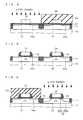
- FIGS. 1 through 9illustrate steps of manufacturing a semiconductor device according to the first preferred embodiment of the present invention.
- the left halfshows a region for forming an nMOS transistor (hereinafter called as an “nMOS region”)
- the right halfshows a region for forming a pMOS transistor (hereinafter called as a “pMOS region”).
- an element isolation film 1 , a p-well 12 , and an n-well 22are provided on a silicon substrate 10 by the conventional technique. Thereafter a silicon oxide film 31 as a gate insulating film is provided thereon. Subsequently, a silicon film 32 for forming gate electrodes is provided on the silicon oxide film 31 (FIG. 1).
- the silicon film 32is not of a single crystalline structure, but either of an amorphous or polycrystalline structure.
- the non-single crystalline silicon film 32is patterned by photolithography, to form gate electrodes 14 and 24 on the p-well 12 and on the n-well 22 , respectively (FIG. 2).
- a resist mask 33is formed by photolithography to have an opening in the pMOS region.
- p-type dopants having a relatively small mass numbersuch as B ions are then implanted, whereby a p-type source/drain extension layer 26 a is formed in the n-well 22 at a relatively shallow depth (FIG. 3).
- ionsare also implanted into the gate electrode 24 , and therefore, non-single crystalline silicon forming the gate electrode 24 is partially amorphized.
- the degree of amorphization thus causedis low due to the relatively small mass number of the implanted ions.
- a resist mask 34is formed by photolithography to have an opening in the nMOS region.
- n-type dopants having a relatively large mass numbersuch as As ions or Sb ions are then implanted, whereby an n-type source/drain extension layer 16 a is formed in the p-well 12 at a relatively shallow depth (FIG. 4).
- ions of a relatively large mass numberare also implanted into the gate electrode 14 . Accordingly, non-single crystalline silicon forming the gate electrode 14 is partially amorphized.
- sidewalls 15 and 25are provided on the respective side surfaces of the gate electrodes 14 and 24 . Further, the silicon oxide film 31 is etched, to form gate insulating films 13 and 23 under the gate electrodes 14 and 24 , respectively (FIG. 5).
- the deposition temperature for the sidewalls 15 and 25is set to be less than the one at which recrystallization of silicon starts (about 550° C.).
- another resist mask 35is formed to have an opening in the pMOS region.
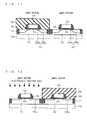
- p-type dopants having a relatively small mass numbersuch as B ions are then implanted with a dose of 4 ⁇ 10 15 /cm 2 or more, whereby a p-type source/drain diffusion layer 26 b is formed in the n-well 22 at a relatively great depth (FIG. 6).
- the p-type source/drain extension layer 26 a and the p-type source/drain diffusion layer 26 bform a p-type source/drain region 26 .
- ionsare also implanted into the gate electrode 24 , and therefore, non-single crystalline silicon forming the gate electrode 24 is partially amorphized.
- the degree of amorphization thus causedis low due to the relatively small mass number of the implanted ions.
- a resist mask 36is formed to have an opening in the nMOS region.
- n-type dopants having a relatively large mass numbersuch as As ions or Sb ions are then implanted with a dose of 4 ⁇ 10 15 /cm 2 or more, whereby an n-type source/drain diffusion layer 16 b is formed in the p-well 12 at a relatively great depth (FIG. 7).
- the n-type source/drain extension layer 16 a and the n-type source/drain diffusion layer 16 bform an n-type source/drain region 16 .
- ions of a relatively large mass numberare also implanted into the gate electrode 14 , and therefore, amorphization of non-single crystalline silicon forming the gate electrode 14 further proceeds.
- a silicon oxide film 40is provided on the gate electrodes 14 and 24 , and on the sidewalls 15 and 25 at a temperature which is less than the one at which recrystallization of silicon starts (about 550° C.) (FIG. 8).
- thermal processingsuch as RTA (rapid thermal annealing) is performed on the silicon oxide film 40 covering the gate electrodes 14 and 24 , and the sidewalls 15 and 25 , at a temperature ranging between about 950° C. and 1100° C.
- the period of this thermal processingmay be 30 seconds or less including momentary annealing (spike annealing).
- momentary annealingspike annealing
- Those ions of a relatively large mass number (70 or more) such as As ions or Sb ionsare implanted in large quantity into the gate electrode 14 of the nMOS transistor.
- the gate electrode 14tends to expand.
- the gate electrode 14can hardly expand. The tendency of the gate electrode 14 to expand causes high compressive residual stress as internal stress therein, thus applying tensile stress to a channel region defined under the gate electrode 14 .
- the silicon oxide film 40is removed, and thereafter, a metal film such as Co film is entirely deposited by sputtering.
- thermal processingis performed at a relatively low temperature of about 350° C. to 550° C., whereby this metal film is reacted with the gate electrodes 14 and 24 , and with the source/drain regions 16 and 26 .
- unreacted metal film remaining on the element isolation film 11 , and on the sidewalls 15 , 25is selectively removed, followed by high-temperature thermal processing.
- silicide layers 14 a and 24 aare formed in the upper portions of the gate electrodes 14 and 24 , respectively, and silicide layers 16 c and 26 c are formed in the upper portions of the source/drain regions 16 and 26 , respectively (FIG. 9).
- predetermined device elementsincluding interlayer insulating film, contact, interconnect line, and the like, are provided, which is the completion of the manufacturing process of the semiconductor device.
- FIGS. 10Aillustrates stress distribution in cross section in a direction of channel length in the nMOS transistor according to the first preferred embodiment
- FIG. 10Billustrates stress distribution in cross section in a direction of channel length of the background-art nMOS transistor, namely, the transistor including the gate electrode 14 into which only ions of a relatively small mass number are implanted. It is seen that in the nMOS transistor of the first preferred embodiment, high compressive residual stress is exerted on the gate electrode 14 , and tensile stress is applied to the channel region. Therefore, the lattice spacing of silicon in the channel region of the nMOS transistor is widened and carrier mobility is enhanced, resulting in improvement in characteristic of the MOS transistor.
- ions (for formation of the n-type source/drain region 16 ) to be implanted into the gate electrode 14have a relatively large mass number
- ions (for formation of the p-type source/drain region 26 ) to be implanted into the gate electrode 24have a relatively small mass number.
- the degrees of stress to be applied to the respective channel regions of the nMOS and pMOS transistorscan vary therebetween. Namely, formation of the nMOS and pMOS transistors does not require separate steps, allowing simplification of the manufacturing steps.
- the exemplary dose of ions for forming the n-type source/drain diffusion layer 16 bis 4 ⁇ 10 15 /cm 2 or more, which is the standard amount therefor.
- the applicability of the present inventionis not limited to this.
- the dose of approximately 4 ⁇ 10 15 /cm 2is sufficient enough to maintain effectiveness of the present invention.
- increased effectivenesscan be achieved by the greater amount.
- the compressive stress on the gate electrode 14 itselfis generated with a dose less than 4 ⁇ 10 15 /cm 2 .
- the silicon oxide film 40is provided as a predetermined film to be on the gate electrodes 14 and 24 .
- the temperature for forming this filmsatisfies the condition that it should be less than the one for starting recrystallization of silicon (about 550° C.)
- alternative materialsmay be used for this predetermined film.
- alternative filmssuch as metal film, silicide film, or stacked film thereof, may be employed. In this case, after compressive residual stress is exerted on the gate electrode 14 by thermal processing, this alternative film is removed. Thereafter, an insulating film such as silicon oxide film is further provided.
- the compressive residual stress exerted on the gate electrode 14also becomes greater when the predetermined film 40 has a property that it shrinks by the foregoing thermal processing (a silicon oxide film has such property). It is confirmed by the present inventors that the higher the temperature for the thermal processing for recrystallization of amorphous silicon, and the greater the thickness of the predetermined film 40 , the greater the compressive residual stress on the gate electrode 14 , whereby improved carrier mobility is provided.
- an ordinary silicon substrateis used for forming a MOS transistor.
- itmay be a “strained silicon substrate” as discussed in the foregoing description of the background art.
- carrier mobility in the channel region of the nMOS transistorcan be reliably improved to a greater degree.
- ions having a relatively small mass numberare implanted into the gate electrode 24 , and therefore, there will be little residual stress to be applied to the gate electrode 24 even with the existence of the silicon oxide film 40 thereon. In the case of ion implantation in large quantity, however, there may be some compressive residual stress to be exerted on the gate electrode 24 even when the implanted ions have a small mass number.
- Thermal processingis thereafter performed at a temperature ranging between about 950° C. and 1100° C., to repair damage and to activate the dopants. At the same time, recrystallization of amorphous silicon occurs, whereby the gate electrodes 14 and 24 turn into polysilicon.
- the surfaces of the gate electrode 24 and the sidewall 25 of the pMOS transistorare exposed without being covered with the silicon oxide film 40 . Accordingly, even when the gate electrode 24 expands slightly, there will be little residual stress on the gate electrode 24 . As a result, as compared with the first preferred embodiment, tensile stress to be exerted on the channel region of the pMOS transistor can be suppressed to a greater degree.
- ion implantation for forming the n-type source/drain diffusion layer 16 bis also operative to implant ions into the gate electrode 14 for expansion thereof.
- ion implantation step into the gate electrode 14may be performed separately from the implantation step for formation of the n-type source/drain diffusion layer 16 b.
- nMOS and pMOS transistorsare provided.
- a resist mask 36is formed to have an opening in the pMOS region.
- electrically inactive ions having a relatively large mass number (70 or more)such as Ge ions are entirely implanted with a dose of 4 ⁇ 10 15 /cm 2 or more, as shown in FIG. 12.
- ionsare implanted into the source/drain region of the nMOS transistor as well as into the gate electrode 14 .
- Those ions implanted in this stepare electrically inactive, and therefore, they are not operative to serve as dopants.
- n-type dopantsare implanted to form the n-type source/drain diffusion layer 16 b .
- the n-type dopants to be implanted in this stepmay be those having a relatively small mass number such as P ions.
- the subsequent stepsare the same as those of the first preferred embodiment. Namely, the silicon oxide film 40 is provided on the gate electrodes 14 and 24 , and on the sidewalls 15 and 25 , and thereafter, thermal processing is performed at a temperature ranging between about 950° C. and 1100° C. As a result, recrystallization of amorphous silicon occurs, whereby the gate electrodes 14 and 24 turn into polysilicon.
- electrically inactive ions having a relatively large mass numberare implanted in large quantity into the gate electrode 14 of the nMOS transistor. Further, the surfaces of the gate electrode 14 and the sidewall 15 are covered with the silicon oxide film 40 . Accordingly, the tendency of the gate electrode 14 to expand causes compressive residual stress as internal stress therein, thus applying tensile stress to the channel region under the gate electrode 14 .
- crystal defectIn a silicon substrate subjected to high stress applied thereto, crystal defect generally occurs with high probability.
- increase in leakage currentsuch as junction leakage current, gate current, or subthreshold leakage current, may occur. That is, the nMOS transistor of the present invention may encounter the problem of crystal defect resulting from tensile stress applied to the channel region. Therefore, the nMOS transistor of the present invention may suffer from an increased amount of leakage current as compared with the one in the background art.
- a logic section of an ordinary semiconductor deviceis intended mainly for high-speed operation and response, giving priority to high-speed operation even with the existence of some leakage current.
- a memory section of an SRAM or DRAMor in a logic section of an LSI for mobile communication system, for example, even slight increase in power consumption resulting from leakage current should be controlled.
- the MOS transistor according to the present inventionmay provide effectiveness for a circuit section placing priority to high-speed operation (hereinafter referred to as a “high-speed circuit section”), while it may be unsuitable for a circuit section requiring suppression of power consumption (hereinafter referred to as a “low-power circuit section”).
- FIGS. 13 through 16illustrate steps of manufacturing a semiconductor device according to the fourth preferred embodiment of the present invention.
- the left halfshows a high-speed circuit section placing priority to high-speed operation
- the right halfshows a low-power circuit section requiring suppression of power consumption.
- the high-speed circuit section and the low-power circuit sectioneach comprise an nMOS region for forming an nMOS transistor and a pMOS region for forming a pMOS transistor
- the steps of manufacturing a semiconductor device according to the fourth preferred embodimentwill be given.
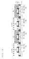
- an element isolation film 11 , p-wells 12 and 52 , and n-wells 22 and 62are provided on a silicon substrate 10 by the conventional technique. Thereafter, following the same steps as those of the first preferred embodiment shown in FIGS. 1 through 5, a gate insulating film 13 , a gate electrode 14 , a sidewall 15 , and an n-type source/drain extension layer 16 a are provided in the nMOS region of the high-speed circuit section.
- a gate insulating film 23 , a gate electrode 24 , a sidewall 25 , and a p-type source/drain extension layer 26 aare provided in the pMOS region of the high-speed circuit section.
- a gate insulating film 53Provided in the nMOS region of the low-power circuit section are a gate insulating film 53 , a gate electrode 54 , a sidewall 55 , and an n-type source/drain extension layer 56 a . Further, a gate insulating film 63 , a gate electrode 64 , a sidewall 65 , and a p-type source/drain extension layer 66 a are provided in the pMOS region of the low-power circuit section.
- a resist mask 71is formed to have an opening in the respective pMOS regions of the high-speed circuit section and the low-power circuit section.
- p-type dopants having a relatively small mass numbersuch as B ions are then implanted with a dose of 4'10 15 /cm 2 or more, whereby a p-type source/drain diffusion layer 26 b and a p-type source/drain diffusion layer 66 b are formed (FIG. 13).
- the p-type source/drain extension layer 26 a and the p-type source/drain diffusion layer 26 bform a p-type source/drain region 26
- the p-type source/drain extension layer 66 a and the p-type source/drain diffusion layer 66 bform a source/drain region 66 .
- ionsare also implanted into the gate electrodes 24 and 64 .
- a resist mask 72is formed to have an opening in the respective nMOS regions of the high-speed circuit section and the low-power circuit section.
- n-type dopants having a relatively large mass numbersuch as As ions or Sb ions are implanted, whereby an n-type source/drain diffusion layer 16 b and an n-type source/drain diffusion layer 56 b are formed (FIG. 14).
- n-type source/drain extension layer 16 a and the n-type source/drain diffusion layer 16 bform an n-type source/drain region 16
- the n-type source/drain extension layer 56 a and the n-type source/drain diffusion layer 56 bform an n-type source/drain region 56 .
- ionsare also implanted into the gate electrodes 14 and 54 .
- a silicon oxide film 80is provided to cover the high-speed circuit section while exposing the low-power circuit section. More particularly, the silicon oxide film 80 is provided on the gate electrodes 14 and 24 , and on the sidewalls 15 and 25 of the high-speed circuit section, at a temperature which is less than the one at which recrystallization of silicon starts (about 550° C.) (FIG. 15).
- Those ions of a relatively large mass number (70 or more) such as As ions or Sb ionsare implanted in large quantity into the gate electrode 14 of the nMOS transistor of the high-speed circuit section. Further, the surfaces of the gate electrode 14 and the sidewall 15 are covered with the silicon oxide film 80 . As a result, high compressive residual stress is exerted as internal stress on the gate electrode 14 , thus applying tensile stress to the channel region under the gate electrode 14 .
- Those ions of a relatively large mass numbersuch as As ions or Sb ions are further implanted in large quantity into the gate electrode 54 of the nMOS transistor of the low-power circuit section.
- the surfaces of the gate electrode 54 and the sidewall 55are exposed, whereby little residual stress is exerted on the gate electrode 54 .
- high tensile stressis applied only to the channel region of the nMOS transistor of the high-speed circuit section, thus allowing performance improvement. Further, substantially no stress is applied to the channel region of the pMOS transistor of the high-speed circuit section, and to the respective channel regions of the pMOS and nMOS transistors of the low-power circuit section, whereby increase in leakage current resulting from crystal defect can be controlled.
- a metal film such as Co filmis deposited by sputtering, followed by thermal processing at a relatively low temperature ranging between 350° C. and 550° C., whereby the metal film and silicon are reacted. Then unreacted metal film remaining on the insulating film is selectively removed. Thereafter high-temperature thermal processing follows.
- silicidation of the gate electrode and source/drain region of the MOS transistor of the low-power circuit sectionis required in many cases.
- the silicon oxide film 80 provided in the foregoing step to cover the high-speed circuit section while exposing the low-power circuit sectionmay be further operative to serve as a mask.
- silicide layers 54 a and 64 aare formed in the upper portions of the gate electrodes 54 and 64 of the low-power circuit section, respectively, and silicide layers 56 c and 66 c are formed in the upper portions of the source/drain regions 56 and 66 of the low-power circuit section, respectively.
- the silicon oxide film 80has such a shape that the low-power circuit section is exposed. Therefore, application of high tensile stress can be limited to the channel region of the nMOS transistor of the high-speed circuit section. That is, even when the gate electrodes 14 , 24 , 54 and 64 are all provided in the same step, only a channel region of a certain nMOS transistor can be subjected to high tensile stress applied thereto. As a result, simplification of the manufacturing steps is realized.
- the MOS transistor according to the present inventionis applied only to a high-speed section of a semiconductor device, while the conventional MOS transistor is applied to a low-power section thereof.
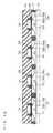
- FIGS. 17 through 20illustrate steps of manufacturing a semiconductor device according to the fifth preferred embodiment. Similar to FIG. 13, in each one of FIGS. 17 through 20, the left half shows a high-speed circuit section placing priority to high-speed operation, and the right half shows a low-power circuit section requiring suppression of power consumption.
- the high-speed circuit section and the low-power circuit sectioneach comprise nMOS and pMOS regions.
- an element isolation film 11 , p-wells 12 and 52 , and n-wells 22 and 62are provided on a silicon substrate 10 .
- a gate insulating film 13 , a gate electrode 14 , a sidewall 15 , and an n-type source/drain extension layer 16 aare provided in the nMOS region of the high-speed circuit section.
- a gate insulating film 23Provided in the pMOS region of the high-speed circuit section are a gate insulating film 23 , a gate electrode 24 , a sidewall 25 , and a p-type source/drain extension layer 26 a .
- a gate insulating film 53Provided in the nMOS region of the low-power circuit section are a gate insulating film 53 , a gate electrode 54 , a sidewall 55 , and an n-type source/drain extension layer 56 a .
- a gate insulating film 63 , a gate electrode 64 , a sidewall 65 , and a p-type source/drain extension layer 66 aare provided in the pMOS region of the low-power circuit section.
- n-type dopants having a relatively small mass numbersuch as P ions are implanted.
- a resist mask 71is formed to have an opening in the respective pMOS regions of the high-speed circuit section and the low-power circuit section.
- p-type dopants having a relatively small mass numbersuch as B ions are then implanted with a dose of 4 ⁇ 10 15 /cm 2 or more, whereby a p-type source/drain diffusion layer 26 b and a p-type source/drain diffusion layer 66 b are formed (FIG. 13).
- the p-type source/drain extension layer 26 a and the p-type source/drain diffusion layer 26 bform a p-type source/drain region 26
- the p-type source/drain extension layer 66 a and the p-type source/drain diffusion layer 66 bform a source/drain region 66 .
- ionsare also implanted into the gate electrodes 24 and 64 .
- a resist mask 73is formed to have an opening in the nMOS region of the low-power circuit section.
- the gate electrode 54 and the sidewall 55as a mask, n-type dopants having a relatively small mass number such as P ions are implanted, whereby an n-type source/drain diffusion layer 56 b is formed (FIG. 17).
- the n-type source/drain extension layer 56 a and the n-type source/drain diffusion layer 56 bform an n-type source/drain region 56 .
- ionsare also implanted into the gate electrode 54 .
- a resist mask 74is formed to have an opening in the nMOS region of the high-speed circuit section.
- n-type dopants having a relatively large mass numbersuch as As ions or Sb ions are implanted, whereby an n-type source/drain diffusion layer 16 b is formed (FIG. 18).
- the n-type source/drain extension layer 16 a and the n-type source/drain diffusion layer 16 bform an n-type source/drain region 16 .
- ionsare also implanted into the gate electrode 14 .
- a silicon oxide film 81is provided to cover the high-speed circuit section and the low-power circuit section. More particularly, the silicon oxide film 81 is provided on the gate electrodes 14 , 24 , 54 and 64 , and on the sidewalls 15 , 25 , 55 and 65 , at a temperature which is less than the one at which recrystallization of silicon starts (about 550° C.)(FIG. 19).
- Those ions of a relatively large mass number (70 or more) such as As ions or Sb ionsare implanted into the gate electrode 14 of the nMOS transistor of the high-speed circuit section. Further, the surfaces of the gate electrode 14 and the sidewall 15 are covered with the silicon oxide film 81 . As a result, high compressive residual stress is exerted as internal stress on the gate electrode 14 , thus applying tensile stress to the channel region under the gate electrode 14 .
- high tensile stressis applied only to the channel region of the nMOS transistor of the high-speed circuit section, thus allowing performance improvement. Further, substantially no stress is applied to the channel region of the pMOS transistor of the high-speed circuit section, and to the respective channel regions of the pMOS and nMOS transistors of the low-power circuit section, whereby increase in leakage current resulting from crystal defect can be controlled.
- an openingis defined in the silicon oxide film 81 to expose the low-power circuit section.
- silicidationis performed.
- silicide layers 54 a and 64 aare formed in the upper portions of the gate electrodes 54 and 64 of the low-power circuit section, respectively, and silicide layers 56 c and 66 c are formed in the upper portions of the source/drain regions 56 and 66 of the low-power circuit section, respectively.
- n-type dopants to be implanted into the high-speed circuit section and into the low-power circuit sectionhave different mass numbers therebetween. Therefore, application of high tensile stress can be limited to the channel region of the nMOS transistor of the high-speed circuit section. That is, even when the gate electrodes 14 , 24 , 54 and 64 are all provided in the same step, only a channel region of a certain nMOS transistor can be subjected to high tensile stress applied thereto.
- the nMOS transistor according to the present inventionis likely to suffer from crystal defect, which may result in leakage current such as junction leakage current, gate current, or subthreshold leakage current of the MOS transistor. That is, the nMOS transistor of the present invention will suffer from an increased amount of leakage current as compared with the one in the background art.
- the sixth preferred embodiment of the present inventionis directed to solve this problem.
- the surfaces of the gate electrodes 14 and 24 , and of the silicon substrate 10are oxidized. More precisely, the silicon oxide film 31 remains on the silicon substrate 10 at this time, and therefore, it is reoxidized.
- the resultant structureis as given in FIG. 21, in which a silicon oxide film 90 is provided on the surfaces of the gate electrodes 14 and 24 , and bird's beaks 90 a are defined at respective edge portions of the gate electrodes 14 and 24 .
- the subsequent stepsare the same as those of FIGS. 3 through 9, and therefore, the description thereof is omitted.
- the insulating filmhas a larger thickness at the edge portions of the gate electrodes 14 and 24 , providing suppression of tunneling current and relaxation of gate electric field.
- subthreshold leakage currentcan be reduced, allowing suppression of increase in leakage current of the MOS transistor.
- the sixth preferred embodimentis effectively applied to the MOS transistor having a probability of increase in leakage current, especially to the nMOS transistor of the present invention subjected to tensile stress applied to its channel region.
Landscapes
- Engineering & Computer Science (AREA)
- Physics & Mathematics (AREA)
- Manufacturing & Machinery (AREA)
- Condensed Matter Physics & Semiconductors (AREA)
- General Physics & Mathematics (AREA)
- Computer Hardware Design (AREA)
- Microelectronics & Electronic Packaging (AREA)
- Power Engineering (AREA)
- High Energy & Nuclear Physics (AREA)
- Health & Medical Sciences (AREA)
- Toxicology (AREA)
- Metal-Oxide And Bipolar Metal-Oxide Semiconductor Integrated Circuits (AREA)
- Insulated Gate Type Field-Effect Transistor (AREA)
- Chemical & Material Sciences (AREA)
- Crystallography & Structural Chemistry (AREA)
- Materials Engineering (AREA)
- Electrodes Of Semiconductors (AREA)
Abstract
Description
- 1. Field of the Invention[0001]
- The present invention relates to a semiconductor including a MOS (metal oxide semiconductor) field effect transistor, and method of manufacturing the same.[0002]
- 2. Description of the Background Art[0003]
- For a MOS field effect transistor (MOS transistor), increase in drain current as a driving current is one of the ways of improving characteristic of this MOS transistor. Carrier mobility is one of the determinants of drain current. The carrier mobility is virtually controlled by a substrate material, and therefore, it can hardly be changed. On the other hand, it has been found that scattering probability and effective mass of carriers are altered by the change in lattice spacing of substrate atoms, allowing change of carrier mobility.[0004]
- SiGe has wider lattice spacing than Si. In a substrate including SiGe and Si stacked thereon, the lattice spacing of the upper-layer Si is widened accordingly. The substrate including the widened lattice spacing of silicon is called as a “strained silicon substrate”. The strained silicon substrate has a higher carrier mobility than a conventional silicon substrate, providing increase in drain current of a MOS transistor formed thereon. An example of such conventional art is given in the non-patent document 1, Welser et al., “NMOS and PMOS Transistors Fabricated in Strained Silicon/Relaxed Silicon-Germanium Structures”, pp. 1000-1002, International Electron Device Meeting 1992, and in the non-patent document 2, T. Mizuno et al., “High Performance Strained-Si p-MOSFETs on SiGe-on-Insulator Substrates Fabricated by SIMOX Technology”, pp. 934-936, International Electron Device Meeting 1999.[0005]
- On the other hand, the strained silicon substrate encounters the problems as follows which result from use of SiGe as a substrate material: crystal defect and deterioration in surface roughness caused by SiGe, rise in substrate temperature due to low heat conductivity of SiGe, increase in short-channel effect in a p-channel MOS transistor covering band discontinuity at an interface between SiGe and Si, or the like. Other problems involved therein associated with process steps include inapplicability to STI (shallow trench isolation) technique, or insufficient activation annealing, for example. In view of this, for actually using the strained silicon substrate in LSIs, there remain a lot of problems to be solved.[0006]
- By way of example, Japanese Patent Application Laid-Open No. 2002-93921 (pp. 3-6 and FIGS.[0007]1-19), hereinafter referred to as the patent document 1, discloses that the lattice spacing of silicon of a MOS transistor may be varied by applying stress to a silicon substrate.
- By way of example, tensile stress exerted on a channel region causes increase in driving current of an n-channel MOS transistor (nMOS transistor), while causing reduction in driving current of a p-channel MOS transistor (pMOS transistor). Conversely, compressive stress exerted on the channel region causes increase in driving current of the pMOS transistor, while causing reduction in driving current of the nMOS transistor.[0008]
- As discussed, the strained silicon substrate including SiGe still faces the problems to be solved. Therefore, more simple way has been sought to improve characteristic of a MOS transistor.[0009]
- According to the patent document 1, stress exerted to a gate electrode is applied to a channel region of a silicon substrate. As a result, channel characteristic of a MOS transistor is improved without the need of preparing a strained silicon substrate.[0010]
- As discussed, tensile stress exerted on a channel region causes increase in driving current of an nMOS transistor, while causing reduction in driving current in a pMOS transistor. In contrast, compressive stress exerted on the channel region causes increase in driving current of the pMOS transistor, while causing reduction in driving current of the nMOS transistor. Therefore, stress to be exerted should differ at least between the nMOS and pMOS transistors.[0011]
- It is thus required in the patent document 1 to employ different gate electrode materials and different deposition temperatures thereof between the nMOS and pMOS transistors. As a result, a gate electrode of the nMOS transistor and that of the pMOS transistor cannot be provided in the same process step, causing complication of the manufacturing steps.[0012]
- It is therefore an object of the present invention to provide a semiconductor device allowing improvement in carrier mobility by applying tensile stress only to a channel region of a desired MOS transistor, and allowing simplification of manufacturing steps. It is still an object of the present invention to provide a method of this semiconductor device.[0013]
- According to a first aspect of the present invention, the semiconductor device includes a polysilicon gate electrode provided on a silicon substrate. The gate electrode is subjected to compressive stress as internal stress therein, to apply tensile stress to the silicon substrate. Ions having a mass number of 70 or more are implanted into the gate electrode.[0014]
- Tensile stress is applied to a region in the silicon substrate defined under a predetermined gate electrode. Therefore, lattice spacing is widened in this region of the silicon substrate. When this gate electrode is applied to an nMOS transistor, for example, enhancement of carrier mobility can be provided, thus contributing to performance improvement of the nMOS transistor.[0015]
- According to a second aspect of the present invention, the method of manufacturing a semiconductor device includes the following steps (a) through (d). In the step (a), a non-single crystalline silicon gate electrode is provided on a silicon substrate. In the step (b), ions having a mass number of 70 or more are implanted into the gate electrode. In the step (c), a predetermined film is deposited at a temperature of 550° C. or less, to cover the gate electrode including therein the ions having a mass number of 70 or more. In the step (d), thermal processing is performed at a temperature of more than 550° C. while covering the gate electrode with the predetermined film.[0016]
- Compressive residual stress is exerted on a predetermined gate electrode as internal stress therein, to apply tensile stress to a region in the silicon substrate defined under the gate electrode. Therefore, lattice spacing is widened in this region of the silicon substrate. When this gate electrode is applied to an nMOS transistor, for example, enhancement of carrier mobility can be provided, thus contributing to performance improvement of the nMOS transistor. Further, a mass number of ion to be implanted may vary according to the type of the gate electrode, or a part of the predetermined film on the predetermined gate electrode may be removed prior to thermal processing. Therefore, even when a plurality of gate electrodes are formed in the same step, only a desired gate electrode can easily be subjected to high compressive stress exerted thereon. As a result, simplification of the manufacturing steps is provided.[0017]
- These and other objects, features, aspects and advantages of the present invention will become more apparent from the following detailed description of the present invention when taken in conjunction with the accompanying drawings.[0018]
- FIGS. 1 through 9 illustrate steps of manufacturing a semiconductor device according to a first preferred embodiment of the present invention;[0019]
- FIGS. 10A and 10B illustrate stress distribution in a direction of channel length in an nMOS transistor of the semiconductor device according to the first preferred embodiment of the present invention, and in the nMOS transistor of the background-art semiconductor device, respectively;[0020]
- FIG. 11 illustrates a step of manufacturing a semiconductor device according to a second preferred embodiment of the present invention;[0021]
- FIG. 12 illustrate a step of manufacturing a semiconductor device according to a third preferred embodiment of the present invention;[0022]
- FIGS. 13 through 16 illustrate steps of manufacturing a semiconductor device according to a fourth preferred embodiment of the present invention;[0023]
- FIGS. 17 through 20 illustrate steps of manufacturing a semiconductor device according to a fifth preferred embodiment of the present invention; and[0024]
- FIG. 21 illustrates a step of manufacturing a semiconductor device according to a sixth preferred embodiment of the present invention.[0025]
- First Preferred Embodiment[0026]
- The present inventors have found that when amorphous silicon including a large number of ions implanted therein undergoes thermal processing to form recrystallized polycrystalline silicon (polysilicon), volume expansion of silicon occurs. It has also been found that the amount of expansion of silicon is controlled largely by the mass number of ions implanted therein, and more particularly, that the amount of expansion increases as the mass number of implanted ions becomes larger (more specifically, 70 or more). It has been confirmed as well that the amount of expansion increases as the implant dose of ions increases.[0027]
- FIGS. 1 through 9 illustrate steps of manufacturing a semiconductor device according to the first preferred embodiment of the present invention. In each one of FIGS. 1 through 9, the left half shows a region for forming an nMOS transistor (hereinafter called as an “nMOS region”), and the right half shows a region for forming a pMOS transistor (hereinafter called as a “pMOS region”).[0028]
- First, an element isolation film[0029]1, a p-
well 12, and an n-well22 are provided on asilicon substrate 10 by the conventional technique. Thereafter asilicon oxide film 31 as a gate insulating film is provided thereon. Subsequently, asilicon film 32 for forming gate electrodes is provided on the silicon oxide film31 (FIG. 1). Thesilicon film 32 is not of a single crystalline structure, but either of an amorphous or polycrystalline structure. - Next, the non-single[0030]
crystalline silicon film 32 is patterned by photolithography, to formgate electrodes - Thereafter, a resist[0031]
mask 33 is formed by photolithography to have an opening in the pMOS region. Using the resistmask 33 and thegate electrode 24 as a mask, p-type dopants having a relatively small mass number such as B ions are then implanted, whereby a p-type source/drain extension layer 26ais formed in the n-well22 at a relatively shallow depth (FIG. 3). At this time, ions are also implanted into thegate electrode 24, and therefore, non-single crystalline silicon forming thegate electrode 24 is partially amorphized. However, the degree of amorphization thus caused is low due to the relatively small mass number of the implanted ions. - Next, a resist[0032]
mask 34 is formed by photolithography to have an opening in the nMOS region. Using the resistmask 34 and thegate electrode 14 as a mask, n-type dopants having a relatively large mass number (70 or more) such as As ions or Sb ions are then implanted, whereby an n-type source/drain extension layer 16ais formed in the p-well12 at a relatively shallow depth (FIG. 4). At this time, ions of a relatively large mass number are also implanted into thegate electrode 14. Accordingly, non-single crystalline silicon forming thegate electrode 14 is partially amorphized. - Thereafter, sidewalls[0033]15 and25 are provided on the respective side surfaces of the
gate electrodes silicon oxide film 31 is etched, to formgate insulating films gate electrodes sidewalls - Subsequently, another resist[0034]
mask 35 is formed to have an opening in the pMOS region. Using the resistmask 35, thegate electrode 24 and thesidewall 25 as a mask, p-type dopants having a relatively small mass number such as B ions are then implanted with a dose of 4×10¹⁵/cm2or more, whereby a p-type source/drain diffusion layer 26bis formed in the n-well22 at a relatively great depth (FIG. 6). The p-type source/drain extension layer 26aand the p-type source/drain diffusion layer 26bform a p-type source/drain region 26. At this time, ions are also implanted into thegate electrode 24, and therefore, non-single crystalline silicon forming thegate electrode 24 is partially amorphized. However, the degree of amorphization thus caused is low due to the relatively small mass number of the implanted ions. - Thereafter, a resist[0035]
mask 36 is formed to have an opening in the nMOS region. Using the resistmask 36, thegate electrode 14 and thesidewall 15 as a mask, n-type dopants having a relatively large mass number such as As ions or Sb ions are then implanted with a dose of 4×10¹⁵/cm2or more, whereby an n-type source/drain diffusion layer 16bis formed in the p-well12 at a relatively great depth (FIG. 7). The n-type source/drain extension layer 16aand the n-type source/drain diffusion layer 16bform an n-type source/drain region 16. At this time, ions of a relatively large mass number are also implanted into thegate electrode 14, and therefore, amorphization of non-single crystalline silicon forming thegate electrode 14 further proceeds. - Subsequently, a[0036]
silicon oxide film 40 is provided on thegate electrodes sidewalls - Next, thermal processing such as RTA (rapid thermal annealing) is performed on the[0037]
silicon oxide film 40 covering thegate electrodes sidewalls gate electrodes - Those ions of a relatively large mass number (70 or more) such as As ions or Sb ions are implanted in large quantity into the[0038]
gate electrode 14 of the nMOS transistor. Hence, thegate electrode 14 tends to expand. However, as the surfaces of thegate electrode 14 and thesidewall 15 are covered with thesilicon oxide film 40, thegate electrode 14 can hardly expand. The tendency of thegate electrode 14 to expand causes high compressive residual stress as internal stress therein, thus applying tensile stress to a channel region defined under thegate electrode 14. - In contrast, only those ions of a relatively small mass number are implanted into the[0039]
gate electrode 24 of the pMOS transistor. Hence, thegate electrode 24 scarcely tends to expand, whereby little residual stress is exerted on thegate electrode 24. As a result, there occurs substantially no stress to be applied to a channel region defined under thegate electrode 24. - As an exemplary way of silicidation of the[0040]
gate electrodes drain regions silicon oxide film 40 is removed, and thereafter, a metal film such as Co film is entirely deposited by sputtering. Next, thermal processing is performed at a relatively low temperature of about 350° C. to 550° C., whereby this metal film is reacted with thegate electrodes drain regions element isolation film 11, and on thesidewalls gate electrodes silicide layers drain regions - Thereafter, predetermined device elements including interlayer insulating film, contact, interconnect line, and the like, are provided, which is the completion of the manufacturing process of the semiconductor device.[0041]
- FIGS. 10A illustrates stress distribution in cross section in a direction of channel length in the nMOS transistor according to the first preferred embodiment, and FIG. 10B illustrates stress distribution in cross section in a direction of channel length of the background-art nMOS transistor, namely, the transistor including the[0042]
gate electrode 14 into which only ions of a relatively small mass number are implanted. It is seen that in the nMOS transistor of the first preferred embodiment, high compressive residual stress is exerted on thegate electrode 14, and tensile stress is applied to the channel region. Therefore, the lattice spacing of silicon in the channel region of the nMOS transistor is widened and carrier mobility is enhanced, resulting in improvement in characteristic of the MOS transistor. - In contrast, little residual stress is exerted on the[0043]
gate electrode 24 of the pMOS transistor, and thus there occurs substantially no stress to be applied to the channel region under thegate electrode 24. As discussed, application of tensile stress to the channel region of the pMOS transistor provides no effectiveness, as it causes reduction in drain current of the pMOS transistor. That is, in the device including both pMOS and nMOS transistors, tensile stress is preferably be applied only to the channel region of the nMOS transistor. In the first preferred embodiment, no tensile stress is applied to the channel region of the pMOS transistor. As a result, while suppressing reduction in drain current of the pMOS transistor, improvement in characteristic of the nMOS transistor is realized. - In addition, in the first preferred embodiment, ions (for formation of the n-type source/drain region[0044]16) to be implanted into the
gate electrode 14 have a relatively large mass number, and ions (for formation of the p-type source/drain region26) to be implanted into thegate electrode 24 have a relatively small mass number. As a result, only the channel region of the nMOS transistor undergoes high tensile stress applied thereto. That is, even when thegate electrodes - As discussed, when amorphous silicon including a large number of ions implanted therein is recrystallized to turn into polysilicon, the tendency of silicon to expand increases as the mass number of the implanted ions increases. Due to this, the greater the mass number of the implanted ions into the[0045]
gate electrode 14, the higher the compressive residual stress thereon. As a result, tensile stress to be applied to the channel region becomes higher, providing enhanced effectiveness of the first preferred embodiment. Further, the compressive residual stress on thegate electrode 14 becomes higher as the dose of the implanted ions implanted therein increases. In the foregoing discussion, the exemplary dose of ions for forming the n-type source/drain diffusion layer 16bis 4×10¹⁵/cm2or more, which is the standard amount therefor. The applicability of the present invention is not limited to this. The dose of approximately 4×10¹⁵/cm2is sufficient enough to maintain effectiveness of the present invention. On the other hand, increased effectiveness can be achieved by the greater amount. The compressive stress on thegate electrode 14 itself is generated with a dose less than 4×10¹⁵/cm2. - In the step of FIG. 8, the[0046]
silicon oxide film 40 is provided as a predetermined film to be on thegate electrodes gate electrode 14, alternative films such as metal film, silicide film, or stacked film thereof, may be employed. In this case, after compressive residual stress is exerted on thegate electrode 14 by thermal processing, this alternative film is removed. Thereafter, an insulating film such as silicon oxide film is further provided. - The compressive residual stress exerted on the[0047]
gate electrode 14 also becomes greater when thepredetermined film 40 has a property that it shrinks by the foregoing thermal processing (a silicon oxide film has such property). It is confirmed by the present inventors that the higher the temperature for the thermal processing for recrystallization of amorphous silicon, and the greater the thickness of thepredetermined film 40, the greater the compressive residual stress on thegate electrode 14, whereby improved carrier mobility is provided. - In the first preferred embodiment, an ordinary silicon substrate is used for forming a MOS transistor. Alternatively, it may be a “strained silicon substrate” as discussed in the foregoing description of the background art. In this case, carrier mobility in the channel region of the nMOS transistor can be reliably improved to a greater degree.[0048]
- Second Preferred Embodiment[0049]
- As discussed in the first preferred embodiment, ions having a relatively small mass number are implanted into the[0050]
gate electrode 24, and therefore, there will be little residual stress to be applied to thegate electrode 24 even with the existence of thesilicon oxide film 40 thereon. In the case of ion implantation in large quantity, however, there may be some compressive residual stress to be exerted on thegate electrode 24 even when the implanted ions have a small mass number. - The steps of manufacturing a semiconductor device according to the second preferred embodiment of the present invention will be given. First, following the same steps as those of the first preferred embodiment shown in FIGS. 1 through 8, the nMOS and pMOS transistors are provided. Further provided thereon is the[0051]
silicon oxide film 40. Next, thesilicon oxide film 40 in the pMOS region is removed so that an opening is defined therein, as shown in FIG. 11. - Thermal processing is thereafter performed at a temperature ranging between about 950° C. and 1100° C., to repair damage and to activate the dopants. At the same time, recrystallization of amorphous silicon occurs, whereby the[0052]
gate electrodes - The surfaces of the[0053]
gate electrode 14 and thesidewall 15 of the nMOS transistor are covered with thesilicon oxide film 40. Therefore, the tendency of thegate electrode 14 to expand causes high compressive residual stress as internal stress therein, thus applying tensile stress to the channel region under thegate electrode 14. - On the other hand, the surfaces of the[0054]
gate electrode 24 and thesidewall 25 of the pMOS transistor are exposed without being covered with thesilicon oxide film 40. Accordingly, even when thegate electrode 24 expands slightly, there will be little residual stress on thegate electrode 24. As a result, as compared with the first preferred embodiment, tensile stress to be exerted on the channel region of the pMOS transistor can be suppressed to a greater degree. - Third Preferred Embodiment[0055]
- In the first and second preferred embodiments, ion implantation for forming the n-type source/[0056]
drain diffusion layer 16bis also operative to implant ions into thegate electrode 14 for expansion thereof. Alternatively, ion implantation step into thegate electrode 14 may be performed separately from the implantation step for formation of the n-type source/drain diffusion layer 16b. - The steps of manufacturing a semiconductor device according to the third preferred embodiment of the present invention will be given. First, following the same steps as those of the first preferred embodiment shown in FIGS. 1 through 6, the nMOS and pMOS transistors are provided. Next, a resist[0057]
mask 36 is formed to have an opening in the pMOS region. Thereafter, prior to formation of the n-type source/drain diffusion layer 16bin the nMOS region, electrically inactive ions having a relatively large mass number (70 or more) such as Ge ions are entirely implanted with a dose of 4×10¹⁵/cm2or more, as shown in FIG. 12. At this time, ions are implanted into the source/drain region of the nMOS transistor as well as into thegate electrode 14. Those ions implanted in this step are electrically inactive, and therefore, they are not operative to serve as dopants. - Thereafter, as shown in FIG. 7, n-type dopants are implanted to form the n-type source/[0058]
drain diffusion layer 16b. The n-type dopants to be implanted in this step may be those having a relatively small mass number such as P ions. - The subsequent steps are the same as those of the first preferred embodiment. Namely, the[0059]
silicon oxide film 40 is provided on thegate electrodes sidewalls gate electrodes - As mentioned, electrically inactive ions having a relatively large mass number are implanted in large quantity into the[0060]
gate electrode 14 of the nMOS transistor. Further, the surfaces of thegate electrode 14 and thesidewall 15 are covered with thesilicon oxide film 40. Accordingly, the tendency of thegate electrode 14 to expand causes compressive residual stress as internal stress therein, thus applying tensile stress to the channel region under thegate electrode 14. - In contrast, only those ions of a relatively small mass number are implanted into the[0061]
gate electrode 24 of the pMOS transistor. Hence, little residual stress is exerted on thegate electrode 24. As a result, there occurs substantially no stress to be applied to the channel region under thegate electrode 24. - Fourth Preferred Embodiment[0062]
- In a silicon substrate subjected to high stress applied thereto, crystal defect generally occurs with high probability. In a transistor provided on the silicon substrate having crystal defect, increase in leakage current such as junction leakage current, gate current, or subthreshold leakage current, may occur. That is, the nMOS transistor of the present invention may encounter the problem of crystal defect resulting from tensile stress applied to the channel region. Therefore, the nMOS transistor of the present invention may suffer from an increased amount of leakage current as compared with the one in the background art.[0063]
- For example, a logic section of an ordinary semiconductor device is intended mainly for high-speed operation and response, giving priority to high-speed operation even with the existence of some leakage current. On the other hand, in a memory section of an SRAM or DRAM, or in a logic section of an LSI for mobile communication system, for example, even slight increase in power consumption resulting from leakage current should be controlled. In view of this, the MOS transistor according to the present invention may provide effectiveness for a circuit section placing priority to high-speed operation (hereinafter referred to as a “high-speed circuit section”), while it may be unsuitable for a circuit section requiring suppression of power consumption (hereinafter referred to as a “low-power circuit section”). In other words, it is preferable to use the MOS transistor of the present invention only in the high-speed circuit section of a semiconductor device, and to use the conventional MOS transistor in the low-power circuit section.[0064]
- FIGS. 13 through 16 illustrate steps of manufacturing a semiconductor device according to the fourth preferred embodiment of the present invention. As indicated in FIG. 13, in each one of FIGS. 13 through 16, the left half shows a high-speed circuit section placing priority to high-speed operation, and the right half shows a low-power circuit section requiring suppression of power consumption. Assuming that the high-speed circuit section and the low-power circuit section each comprise an nMOS region for forming an nMOS transistor and a pMOS region for forming a pMOS transistor, the steps of manufacturing a semiconductor device according to the fourth preferred embodiment will be given.[0065]
- First, an[0066]
element isolation film 11, p-wells wells silicon substrate 10 by the conventional technique. Thereafter, following the same steps as those of the first preferred embodiment shown in FIGS. 1 through 5, agate insulating film 13, agate electrode 14, asidewall 15, and an n-type source/drain extension layer 16aare provided in the nMOS region of the high-speed circuit section. Provided in the pMOS region of the high-speed circuit section are agate insulating film 23, agate electrode 24, asidewall 25, and a p-type source/drain extension layer 26a. Provided in the nMOS region of the low-power circuit section are agate insulating film 53, agate electrode 54, asidewall 55, and an n-type source/drain extension layer 56a. Further, agate insulating film 63, agate electrode 64, asidewall 65, and a p-type source/drain extension layer 66aare provided in the pMOS region of the low-power circuit section. - Subsequently, a resist[0067]
mask 71 is formed to have an opening in the respective pMOS regions of the high-speed circuit section and the low-power circuit section. Using the resistmask 71, thegate electrodes sidewalls drain diffusion layer 26band a p-type source/drain diffusion layer 66bare formed (FIG. 13). The p-type source/drain extension layer 26aand the p-type source/drain diffusion layer 26bform a p-type source/drain region 26, and the p-type source/drain extension layer 66aand the p-type source/drain diffusion layer 66bform a source/drain region 66. At this time, ions are also implanted into thegate electrodes - Next, a resist[0068]
mask 72 is formed to have an opening in the respective nMOS regions of the high-speed circuit section and the low-power circuit section. Using the resistmask 72, thegate electrodes sidewalls drain diffusion layer 16band an n-type source/drain diffusion layer 56bare formed (FIG. 14). The n-type source/drain extension layer 16aand the n-type source/drain diffusion layer 16bform an n-type source/drain region 16, and the n-type source/drain extension layer 56aand the n-type source/drain diffusion layer 56bform an n-type source/drain region 56. At this time, ions are also implanted into thegate electrodes - Next, a[0069]
silicon oxide film 80 is provided to cover the high-speed circuit section while exposing the low-power circuit section. More particularly, thesilicon oxide film 80 is provided on thegate electrodes sidewalls - Thereafter, thermal processing is performed on the[0070]
silicon oxide film 80 covering thegate electrodes sidewalls gate electrodes - Those ions of a relatively large mass number (70 or more) such as As ions or Sb ions are implanted in large quantity into the[0071]
gate electrode 14 of the nMOS transistor of the high-speed circuit section. Further, the surfaces of thegate electrode 14 and thesidewall 15 are covered with thesilicon oxide film 80. As a result, high compressive residual stress is exerted as internal stress on thegate electrode 14, thus applying tensile stress to the channel region under thegate electrode 14. - Those ions of a relatively large mass number such as As ions or Sb ions are further implanted in large quantity into the[0072]
gate electrode 54 of the nMOS transistor of the low-power circuit section. However, the surfaces of thegate electrode 54 and thesidewall 55 are exposed, whereby little residual stress is exerted on thegate electrode 54. As a result, there occurs substantially no stress to be applied to the channel region under thegate electrode 54. - Only those ions of a relatively small mass number are implanted into the[0073]
gate electrodes gate electrodes gate electrodes - As discussed, according to the manufacturing steps of the fourth preferred embodiment, high tensile stress is applied only to the channel region of the nMOS transistor of the high-speed circuit section, thus allowing performance improvement. Further, substantially no stress is applied to the channel region of the pMOS transistor of the high-speed circuit section, and to the respective channel regions of the pMOS and nMOS transistors of the low-power circuit section, whereby increase in leakage current resulting from crystal defect can be controlled.[0074]
- As an exemplary way of silicidation of the gate electrode and source/drain region of a certain MOS transistor, a metal film such as Co film is deposited by sputtering, followed by thermal processing at a relatively low temperature ranging between 350° C. and 550° C., whereby the metal film and silicon are reacted. Then unreacted metal film remaining on the insulating film is selectively removed. Thereafter high-temperature thermal processing follows.[0075]
- In an LSI for mobile communication system, for example, silicidation of the gate electrode and source/drain region of the MOS transistor of the low-power circuit section is required in many cases. For such silicidation, the[0076]
silicon oxide film 80 provided in the foregoing step to cover the high-speed circuit section while exposing the low-power circuit section may be further operative to serve as a mask. After silicidation using thesilicon oxide film 80 as a mask, silicide layers54aand64aare formed in the upper portions of thegate electrodes silicide layers drain regions - According to the fourth preferred embodiment, for recrystallization of amorphous silicon, the[0077]
silicon oxide film 80 has such a shape that the low-power circuit section is exposed. Therefore, application of high tensile stress can be limited to the channel region of the nMOS transistor of the high-speed circuit section. That is, even when thegate electrodes - Fifth Preferred Embodiment[0078]
- Similar to the fourth preferred embodiment, in the fifth preferred embodiment of the present invention, the MOS transistor according to the present invention is applied only to a high-speed section of a semiconductor device, while the conventional MOS transistor is applied to a low-power section thereof.[0079]
- FIGS. 17 through 20 illustrate steps of manufacturing a semiconductor device according to the fifth preferred embodiment. Similar to FIG. 13, in each one of FIGS. 17 through 20, the left half shows a high-speed circuit section placing priority to high-speed operation, and the right half shows a low-power circuit section requiring suppression of power consumption. The high-speed circuit section and the low-power circuit section each comprise nMOS and pMOS regions.[0080]
- The steps of manufacturing the semiconductor device according to the fifth preferred embodiment will be described with reference to FIGS. 17 through 20. First, similar to the fourth preferred embodiment, an[0081]
element isolation film 11, p-wells wells silicon substrate 10. Thereafter, agate insulating film 13, agate electrode 14, asidewall 15, and an n-type source/drain extension layer 16aare provided in the nMOS region of the high-speed circuit section. Provided in the pMOS region of the high-speed circuit section are agate insulating film 23, agate electrode 24, asidewall 25, and a p-type source/drain extension layer 26a. Provided in the nMOS region of the low-power circuit section are agate insulating film 53, agate electrode 54, asidewall 55, and an n-type source/drain extension layer 56a. Further, agate insulating film 63, agate electrode 64, asidewall 65, and a p-type source/drain extension layer 66aare provided in the pMOS region of the low-power circuit section. In the fifth preferred embodiment, for formation of the n-type source/drain extension layers16aand56a, n-type dopants having a relatively small mass number such as P ions are implanted. - Subsequently, a resist[0082]
mask 71 is formed to have an opening in the respective pMOS regions of the high-speed circuit section and the low-power circuit section. Using the resistmask 71, thegate electrodes sidewalls drain diffusion layer 26band a p-type source/drain diffusion layer 66bare formed (FIG. 13). The p-type source/drain extension layer 26aand the p-type source/drain diffusion layer 26bform a p-type source/drain region 26, and the p-type source/drain extension layer 66aand the p-type source/drain diffusion layer 66bform a source/drain region 66. At this time, ions are also implanted into thegate electrodes - Next, a resist[0083]
mask 73 is formed to have an opening in the nMOS region of the low-power circuit section. Using the resistmask 73, thegate electrode 54 and thesidewall 55 as a mask, n-type dopants having a relatively small mass number such as P ions are implanted, whereby an n-type source/drain diffusion layer 56bis formed (FIG. 17). The n-type source/drain extension layer 56aand the n-type source/drain diffusion layer 56bform an n-type source/drain region 56. At this time, ions are also implanted into thegate electrode 54. - Thereafter, a resist[0084]
mask 74 is formed to have an opening in the nMOS region of the high-speed circuit section. Using the resistmask 74, thegate electrode 14 and thesidewall 15 as a mask, n-type dopants having a relatively large mass number such as As ions or Sb ions are implanted, whereby an n-type source/drain diffusion layer 16bis formed (FIG. 18). The n-type source/drain extension layer 16aand the n-type source/drain diffusion layer 16bform an n-type source/drain region 16. At this time, ions are also implanted into thegate electrode 14. - Next, a[0085]
silicon oxide film 81 is provided to cover the high-speed circuit section and the low-power circuit section. More particularly, thesilicon oxide film 81 is provided on thegate electrodes sidewalls - Thereafter, thermal processing is performed on the[0086]
silicon oxide film 81 covering thegate electrodes sidewalls gate electrodes - Those ions of a relatively large mass number (70 or more) such as As ions or Sb ions are implanted into the[0087]
gate electrode 14 of the nMOS transistor of the high-speed circuit section. Further, the surfaces of thegate electrode 14 and thesidewall 15 are covered with thesilicon oxide film 81. As a result, high compressive residual stress is exerted as internal stress on thegate electrode 14, thus applying tensile stress to the channel region under thegate electrode 14. - Only those ions of a relatively small mass number are implanted into the[0088]
gate electrode 54 of the nMOS transistor of the low-power circuit section, whereby little residual stress is exerted on thegate electrode 54. As a result, there occurs substantially no stress to be applied to the channel region under thegate electrode 54. - Only those ions of a relatively small mass number are further implanted into the[0089]
gate electrodes gate electrodes gate electrodes - As discussed, according to the manufacturing steps of the fifth preferred embodiment, high tensile stress is applied only to the channel region of the nMOS transistor of the high-speed circuit section, thus allowing performance improvement. Further, substantially no stress is applied to the channel region of the pMOS transistor of the high-speed circuit section, and to the respective channel regions of the pMOS and nMOS transistors of the low-power circuit section, whereby increase in leakage current resulting from crystal defect can be controlled.[0090]
- In an LSI for mobile communication system, for example, for silicidation of the gate electrode and source/drain region of the MOS transistor of the low-power circuit section, an opening is defined in the[0091]
silicon oxide film 81 to expose the low-power circuit section. Using thissilicon oxide film 81 as a mask, silicidation is performed. As a result, silicide layers54aand64aare formed in the upper portions of thegate electrodes silicide layers drain regions - According to the fifth preferred embodiment, n-type dopants to be implanted into the high-speed circuit section and into the low-power circuit section have different mass numbers therebetween. Therefore, application of high tensile stress can be limited to the channel region of the nMOS transistor of the high-speed circuit section. That is, even when the[0092]
gate electrodes - Sixth Preferred Embodiment[0093]
- As discussed, the nMOS transistor according to the present invention is likely to suffer from crystal defect, which may result in leakage current such as junction leakage current, gate current, or subthreshold leakage current of the MOS transistor. That is, the nMOS transistor of the present invention will suffer from an increased amount of leakage current as compared with the one in the background art. The sixth preferred embodiment of the present invention is directed to solve this problem.[0094]
- By way of example, after the[0095]
gate electrodes gate electrodes silicon substrate 10 are oxidized. More precisely, thesilicon oxide film 31 remains on thesilicon substrate 10 at this time, and therefore, it is reoxidized. The resultant structure is as given in FIG. 21, in which asilicon oxide film 90 is provided on the surfaces of thegate electrodes beaks 90aare defined at respective edge portions of thegate electrodes - Resulting from the existence of the bird's[0096]
beaks 90a, the insulating film has a larger thickness at the edge portions of thegate electrodes - Further, as the[0097]
gate electrodes silicon oxide film 90 during thermal processing to be performed in the subsequent step, variation in resistance value of the polysilicon gate electrodes can be controlled in the non-silicided region. - While the invention has been shown and described in detail, the foregoing description is in all aspects illustrative and not restrictive. It is therefore understood that numerous modifications and variations can be devised without departing from the scope of the invention.[0098]
Claims (18)
Priority Applications (14)
| Application Number | Priority Date | Filing Date | Title |
|---|---|---|---|
| US11/127,093US7183204B2 (en) | 2002-11-20 | 2005-05-12 | Semiconductor device including gate electrode for applying tensile stress to silicon substrate, and method of manufacturing the same |
| US11/671,216US7470618B2 (en) | 2002-11-20 | 2007-02-05 | Semiconductor device including gate electrode for applying tensile stress to silicon substrate, and method of manufacturing the same |
| US12/323,507US7960281B2 (en) | 2002-11-20 | 2008-11-26 | Semiconductor device including gate electrode for applying tensile stress to silicon substrate, and method of manufacturing the same |
| US13/103,558US8372747B2 (en) | 2002-11-20 | 2011-05-09 | Semiconductor device including gate electrode for applying tensile stress to silicon substrate, and method of manufacturing the same |
| US13/743,012US8586475B2 (en) | 2002-11-20 | 2013-01-16 | Semiconductor device including gate electrode for applying tensile stress to silicon substrate, and method of manufacturing the same |
| US14/038,981US8809186B2 (en) | 2002-11-20 | 2013-09-27 | Semiconductor device including gate electrode for applying tensile stress to silicon substrate, and method of manufacturing the same |
| US14/325,570US9209191B2 (en) | 2002-11-20 | 2014-07-08 | Semiconductor device including gate electrode for applying tensile stress to silicon substrate, and method of manufacturing the same |
| US14/933,079US9412867B2 (en) | 2002-11-20 | 2015-11-05 | Semiconductor device including gate electrode for applying tensile stress to silicon substrate, and method of manufacturing the same |
| US15/201,744US9614081B2 (en) | 2002-11-20 | 2016-07-05 | Semiconductor device including gate electrode for applying tensile stress to silicon substrate, and method of manufacturing the same |
| US15/384,000US9847417B2 (en) | 2002-11-20 | 2016-12-19 | Semiconductor device including gate electrode for applying tensile stress to silicon substrate, and method of manufacturing the same |
| US15/806,535US20180069119A1 (en) | 2002-11-20 | 2017-11-08 | Semiconductor device including gate electrode for applying tensile stress to silicon substrate, and method of manufacturing the same |
| US16/835,661US20200227557A1 (en) | 2002-11-20 | 2020-03-31 | Semiconductor device including gate electrode for applying tensile stress to silicon substrate, and method of manufacturing the same |
| US17/353,079US12198987B2 (en) | 2002-11-20 | 2021-06-21 | Semiconductor device including gate electrode for applying tensile stress to silicon substrate, and method of manufacturing the same |
| US18/966,471US20250098281A1 (en) | 2002-11-20 | 2024-12-03 | Semiconductor device including gate electrode for applying tensile stress to silicon substrate, and method of manufacturing the same |
Applications Claiming Priority (2)
| Application Number | Priority Date | Filing Date | Title |
|---|---|---|---|
| JP2002336669AJP2004172389A (en) | 2002-11-20 | 2002-11-20 | Semiconductor device and method of manufacturing the same |
| JP2002-336669 | 2002-11-20 |
Related Child Applications (1)
| Application Number | Title | Priority Date | Filing Date |
|---|---|---|---|
| US11/127,093DivisionUS7183204B2 (en) | 2002-11-20 | 2005-05-12 | Semiconductor device including gate electrode for applying tensile stress to silicon substrate, and method of manufacturing the same |
Publications (2)
| Publication Number | Publication Date |
|---|---|
| US20040097030A1true US20040097030A1 (en) | 2004-05-20 |
| US6906393B2 US6906393B2 (en) | 2005-06-14 |
Family
ID=32290368
Family Applications (15)
| Application Number | Title | Priority Date | Filing Date |
|---|---|---|---|
| US10/620,379Expired - LifetimeUS6906393B2 (en) | 2002-11-20 | 2003-07-17 | Semiconductor device including gate electrode for applying tensile stress to silicon substrate, and method of manufacturing the same |
| US11/127,093Expired - LifetimeUS7183204B2 (en) | 2002-11-20 | 2005-05-12 | Semiconductor device including gate electrode for applying tensile stress to silicon substrate, and method of manufacturing the same |
| US11/671,216Expired - LifetimeUS7470618B2 (en) | 2002-11-20 | 2007-02-05 | Semiconductor device including gate electrode for applying tensile stress to silicon substrate, and method of manufacturing the same |
| US12/323,507Expired - LifetimeUS7960281B2 (en) | 2002-11-20 | 2008-11-26 | Semiconductor device including gate electrode for applying tensile stress to silicon substrate, and method of manufacturing the same |
| US13/103,558Expired - Fee RelatedUS8372747B2 (en) | 2002-11-20 | 2011-05-09 | Semiconductor device including gate electrode for applying tensile stress to silicon substrate, and method of manufacturing the same |
| US13/743,012Expired - LifetimeUS8586475B2 (en) | 2002-11-20 | 2013-01-16 | Semiconductor device including gate electrode for applying tensile stress to silicon substrate, and method of manufacturing the same |
| US14/038,981Expired - LifetimeUS8809186B2 (en) | 2002-11-20 | 2013-09-27 | Semiconductor device including gate electrode for applying tensile stress to silicon substrate, and method of manufacturing the same |
| US14/325,570Expired - LifetimeUS9209191B2 (en) | 2002-11-20 | 2014-07-08 | Semiconductor device including gate electrode for applying tensile stress to silicon substrate, and method of manufacturing the same |
| US14/933,079Expired - Fee RelatedUS9412867B2 (en) | 2002-11-20 | 2015-11-05 | Semiconductor device including gate electrode for applying tensile stress to silicon substrate, and method of manufacturing the same |
| US15/201,744Expired - Fee RelatedUS9614081B2 (en) | 2002-11-20 | 2016-07-05 | Semiconductor device including gate electrode for applying tensile stress to silicon substrate, and method of manufacturing the same |
| US15/384,000Expired - LifetimeUS9847417B2 (en) | 2002-11-20 | 2016-12-19 | Semiconductor device including gate electrode for applying tensile stress to silicon substrate, and method of manufacturing the same |
| US15/806,535AbandonedUS20180069119A1 (en) | 2002-11-20 | 2017-11-08 | Semiconductor device including gate electrode for applying tensile stress to silicon substrate, and method of manufacturing the same |
| US16/835,661AbandonedUS20200227557A1 (en) | 2002-11-20 | 2020-03-31 | Semiconductor device including gate electrode for applying tensile stress to silicon substrate, and method of manufacturing the same |
| US17/353,079Expired - LifetimeUS12198987B2 (en) | 2002-11-20 | 2021-06-21 | Semiconductor device including gate electrode for applying tensile stress to silicon substrate, and method of manufacturing the same |
| US18/966,471PendingUS20250098281A1 (en) | 2002-11-20 | 2024-12-03 | Semiconductor device including gate electrode for applying tensile stress to silicon substrate, and method of manufacturing the same |
Family Applications After (14)
| Application Number | Title | Priority Date | Filing Date |
|---|---|---|---|
| US11/127,093Expired - LifetimeUS7183204B2 (en) | 2002-11-20 | 2005-05-12 | Semiconductor device including gate electrode for applying tensile stress to silicon substrate, and method of manufacturing the same |
| US11/671,216Expired - LifetimeUS7470618B2 (en) | 2002-11-20 | 2007-02-05 | Semiconductor device including gate electrode for applying tensile stress to silicon substrate, and method of manufacturing the same |
| US12/323,507Expired - LifetimeUS7960281B2 (en) | 2002-11-20 | 2008-11-26 | Semiconductor device including gate electrode for applying tensile stress to silicon substrate, and method of manufacturing the same |
| US13/103,558Expired - Fee RelatedUS8372747B2 (en) | 2002-11-20 | 2011-05-09 | Semiconductor device including gate electrode for applying tensile stress to silicon substrate, and method of manufacturing the same |
| US13/743,012Expired - LifetimeUS8586475B2 (en) | 2002-11-20 | 2013-01-16 | Semiconductor device including gate electrode for applying tensile stress to silicon substrate, and method of manufacturing the same |
| US14/038,981Expired - LifetimeUS8809186B2 (en) | 2002-11-20 | 2013-09-27 | Semiconductor device including gate electrode for applying tensile stress to silicon substrate, and method of manufacturing the same |
| US14/325,570Expired - LifetimeUS9209191B2 (en) | 2002-11-20 | 2014-07-08 | Semiconductor device including gate electrode for applying tensile stress to silicon substrate, and method of manufacturing the same |
| US14/933,079Expired - Fee RelatedUS9412867B2 (en) | 2002-11-20 | 2015-11-05 | Semiconductor device including gate electrode for applying tensile stress to silicon substrate, and method of manufacturing the same |
| US15/201,744Expired - Fee RelatedUS9614081B2 (en) | 2002-11-20 | 2016-07-05 | Semiconductor device including gate electrode for applying tensile stress to silicon substrate, and method of manufacturing the same |
| US15/384,000Expired - LifetimeUS9847417B2 (en) | 2002-11-20 | 2016-12-19 | Semiconductor device including gate electrode for applying tensile stress to silicon substrate, and method of manufacturing the same |
| US15/806,535AbandonedUS20180069119A1 (en) | 2002-11-20 | 2017-11-08 | Semiconductor device including gate electrode for applying tensile stress to silicon substrate, and method of manufacturing the same |
| US16/835,661AbandonedUS20200227557A1 (en) | 2002-11-20 | 2020-03-31 | Semiconductor device including gate electrode for applying tensile stress to silicon substrate, and method of manufacturing the same |
| US17/353,079Expired - LifetimeUS12198987B2 (en) | 2002-11-20 | 2021-06-21 | Semiconductor device including gate electrode for applying tensile stress to silicon substrate, and method of manufacturing the same |
| US18/966,471PendingUS20250098281A1 (en) | 2002-11-20 | 2024-12-03 | Semiconductor device including gate electrode for applying tensile stress to silicon substrate, and method of manufacturing the same |
Country Status (4)
| Country | Link |
|---|---|
| US (15) | US6906393B2 (en) |
| JP (1) | JP2004172389A (en) |
| KR (1) | KR100599907B1 (en) |
| TW (1) | TWI260091B (en) |
Cited By (18)
| Publication number | Priority date | Publication date | Assignee | Title |
|---|---|---|---|---|
| US20050059260A1 (en)* | 2003-09-15 | 2005-03-17 | Haowen Bu | CMOS transistors and methods of forming same |
| US20050064646A1 (en)* | 2003-09-23 | 2005-03-24 | Dureseti Chidambarrao | NFETs using gate induced stress modulation |
| US20050136583A1 (en)* | 2003-12-23 | 2005-06-23 | Taiwan Semiconductor Manufacturing Co. | Advanced strained-channel technique to improve CMOS performance |
| US7060549B1 (en)* | 2005-07-01 | 2006-06-13 | Advanced Micro Devices, Inc. | SRAM devices utilizing tensile-stressed strain films and methods for fabricating the same |
| WO2006127465A1 (en)* | 2005-05-26 | 2006-11-30 | Applied Materials, Inc. | Integration process for fabricating stressed transistor structure |
| US20060269693A1 (en)* | 2005-05-26 | 2006-11-30 | Applied Materials, Inc. | Method to increase tensile stress of silicon nitride films using a post PECVD deposition UV cure |
| US20060286758A1 (en)* | 2005-06-17 | 2006-12-21 | Taiwan Semiconductor Manufacturing Company, Ltd. | Super anneal for process induced strain modulation |
| US20070018251A1 (en)* | 2005-07-20 | 2007-01-25 | Junji Hirase | Semiconductor device and method for fabricating the same |
| US20070166936A1 (en)* | 2006-01-19 | 2007-07-19 | Po-Chao Tsao | Pre-amorphization implantation process and salicide process |
| US20080020591A1 (en)* | 2005-05-26 | 2008-01-24 | Applied Materials, Inc. | Method to increase silicon nitride tensile stress using nitrogen plasma in-situ treatment and ex-situ uv cure |
| US20080185667A1 (en)* | 2004-09-17 | 2008-08-07 | Kenichi Yoshino | Thin Film Semiconductor Device and Method for Manufacturing the Same |
| EP1815506A4 (en)* | 2004-11-11 | 2009-06-10 | Ibm | METHOD FOR IMPROVING CMOS TRANSISTOR PERFORMANCE BY INTRODUCING LINE IN GATE AND CHANNEL |
| US20090176343A1 (en)* | 2005-03-09 | 2009-07-09 | Fujitsu Microelectronics Limited | P-channel MOS transistor and fabrication process thereof |
| US20090206407A1 (en)* | 2008-02-19 | 2009-08-20 | Anderson Brent A | Semiconductor devices having tensile and/or compressive stress and methods of manufacturing |
| US20100078729A1 (en)* | 2007-03-27 | 2010-04-01 | Fujitsu Microelectronics Limited | Semiconductor device and method of manufacturing the semiconductor device |
| US20110147852A1 (en)* | 2004-03-30 | 2011-06-23 | Samsung Electronics Co., Ltd. | Low noise and high performance lsi device, layout and manufacturing method |
| CN103177947A (en)* | 2011-12-22 | 2013-06-26 | 无锡华润上华科技有限公司 | Method for preparing polysilicon gate electrode of Metal Oxide Semiconductor (MOS) transistor |
| US9018108B2 (en) | 2013-01-25 | 2015-04-28 | Applied Materials, Inc. | Low shrinkage dielectric films |
Families Citing this family (43)
| Publication number | Priority date | Publication date | Assignee | Title |
|---|---|---|---|---|
| JP2004172389A (en) | 2002-11-20 | 2004-06-17 | Renesas Technology Corp | Semiconductor device and method of manufacturing the same |
| US7122849B2 (en)* | 2003-11-14 | 2006-10-17 | International Business Machines Corporation | Stressed semiconductor device structures having granular semiconductor material |
| US7227205B2 (en)* | 2004-06-24 | 2007-06-05 | International Business Machines Corporation | Strained-silicon CMOS device and method |
| US7157355B2 (en)* | 2004-06-30 | 2007-01-02 | Freescale Smeiconductor, Inc. | Method of making a semiconductor device having a strained semiconductor layer |
| US7253045B1 (en)* | 2004-07-13 | 2007-08-07 | Advanced Micro Devices, Inc. | Selective P-channel VT adjustment in SiGe system for leakage optimization |
| JP2006041118A (en)* | 2004-07-26 | 2006-02-09 | Toshiba Corp | Semiconductor device and manufacturing method thereof |
| US7169659B2 (en)* | 2004-08-31 | 2007-01-30 | Texas Instruments Incorporated | Method to selectively recess ETCH regions on a wafer surface using capoly as a mask |
| JP2006120718A (en)* | 2004-10-19 | 2006-05-11 | Toshiba Corp | Semiconductor device and manufacturing method thereof |
| US7429775B1 (en) | 2005-03-31 | 2008-09-30 | Xilinx, Inc. | Method of fabricating strain-silicon CMOS |
| US7423283B1 (en) | 2005-06-07 | 2008-09-09 | Xilinx, Inc. | Strain-silicon CMOS using etch-stop layer and method of manufacture |
| WO2007010600A1 (en)* | 2005-07-20 | 2007-01-25 | Fujitsu Limited | Semiconductor device and its manufacturing method |
| JP4486056B2 (en)* | 2005-07-20 | 2010-06-23 | パナソニック株式会社 | Semiconductor device and manufacturing method thereof |
| KR101155097B1 (en)* | 2005-08-24 | 2012-06-11 | 삼성전자주식회사 | Fabricating method for semiconductor device and semiconductor device fabricated by the same |
| US7655991B1 (en)* | 2005-09-08 | 2010-02-02 | Xilinx, Inc. | CMOS device with stressed sidewall spacers |
| US7936006B1 (en) | 2005-10-06 | 2011-05-03 | Xilinx, Inc. | Semiconductor device with backfilled isolation |
| US20070108529A1 (en)* | 2005-11-14 | 2007-05-17 | Taiwan Semiconductor Manufacturing Company, Ltd. | Strained gate electrodes in semiconductor devices |
| US7566605B2 (en)* | 2006-03-31 | 2009-07-28 | Intel Corporation | Epitaxial silicon germanium for reduced contact resistance in field-effect transistors |
| DE102006019936B4 (en)* | 2006-04-28 | 2015-01-29 | Globalfoundries Inc. | Semiconductor device with differently strained etch stop layers in conjunction with PN junctions of different design in different device areas and method for producing the semiconductor device |
| KR100703986B1 (en)* | 2006-05-22 | 2007-04-09 | 삼성전자주식회사 | Semiconductor device having analog transistor with improved operation characteristics and flicker noise characteristics, and manufacturing method thereof |
| KR100772836B1 (en) | 2006-07-21 | 2007-11-01 | 동부일렉트로닉스 주식회사 | Manufacturing Method of Semiconductor Device |
| US7858529B2 (en) | 2006-12-18 | 2010-12-28 | United Microelectronics Corp. | Treatment method of semiconductor, method for manufacturing MOS, and MOS structure |
| JP2008153515A (en)* | 2006-12-19 | 2008-07-03 | Fujitsu Ltd | MOS transistor, method for manufacturing the MOS transistor, CMOS semiconductor device using the MOS transistor, and semiconductor device using the CMOS semiconductor device |
| JPWO2008078363A1 (en)* | 2006-12-22 | 2010-04-15 | 株式会社ルネサステクノロジ | Semiconductor device manufacturing method and semiconductor device |
| KR100882834B1 (en)* | 2007-03-14 | 2009-02-10 | 샤프 가부시키가이샤 | Thin Film Semiconductor Device and Manufacturing Method Thereof |
| JP5222583B2 (en)* | 2007-04-06 | 2013-06-26 | パナソニック株式会社 | Semiconductor device |
| US7960243B2 (en) | 2007-05-31 | 2011-06-14 | Freescale Semiconductor, Inc. | Method of forming a semiconductor device featuring a gate stressor and semiconductor device |
| KR101264113B1 (en)* | 2007-07-16 | 2013-05-13 | 삼성전자주식회사 | CMOS device having strained channel and method of fabricating the same |
| JP5076771B2 (en)* | 2007-09-21 | 2012-11-21 | 富士通セミコンダクター株式会社 | Manufacturing method of semiconductor device |
| JP2009088069A (en)* | 2007-09-28 | 2009-04-23 | Panasonic Corp | Semiconductor device and manufacturing method thereof |
| DE102007063230B4 (en)* | 2007-12-31 | 2013-06-06 | Advanced Micro Devices, Inc. | Semiconductor device with strained material layers and contact element and method of production thereof |
| DE102008011931B4 (en)* | 2008-02-29 | 2010-10-07 | Advanced Micro Devices, Inc., Sunnyvale | Reduction of memory instability by locally adjusting the recrystallization conditions in a cache area of a semiconductor device |
| US8624295B2 (en) | 2008-03-20 | 2014-01-07 | Taiwan Semiconductor Manufacturing Company, Ltd. | SRAM devices utilizing strained-channel transistors and methods of manufacture |
| JP2010016302A (en)* | 2008-07-07 | 2010-01-21 | Panasonic Corp | Semiconductor device and method of manufacturing the same |
| US7767534B2 (en)* | 2008-09-29 | 2010-08-03 | Advanced Micro Devices, Inc. | Methods for fabricating MOS devices having highly stressed channels |
| JP5463811B2 (en)* | 2009-09-09 | 2014-04-09 | 富士通セミコンダクター株式会社 | Manufacturing method of semiconductor device |
| KR101720072B1 (en)* | 2009-12-11 | 2017-03-27 | 가부시키가이샤 한도오따이 에네루기 켄큐쇼 | Nonvolatile latch circuit and logic circuit, and semiconductor device using the same |
| US8534808B2 (en)* | 2010-02-08 | 2013-09-17 | Seiko Epson Corporation | Liquid ejecting apparatus and cleaning method in liquid ejecting apparatus |
| CN102194748B (en)* | 2010-03-15 | 2014-04-16 | 北京大学 | Semiconductor device and manufacture method thereof |
| DE112012002603B4 (en) | 2011-06-23 | 2017-02-02 | Mitsubishi Electric Corp. | Semiconductor device and method of manufacturing a semiconductor device |
| US9508557B2 (en) | 2014-11-24 | 2016-11-29 | Tokyo Electron Limited | Method of improving line roughness in substrate processing |
| CN108417572A (en)* | 2017-02-10 | 2018-08-17 | 中芯国际集成电路制造(上海)有限公司 | SRAM memory and its forming method |
| CN107783022B (en)* | 2017-10-27 | 2019-10-11 | 西安电子科技大学 | Thermal Reliability Evaluation Method for High Electron Mobility Transistors |
| US12154973B2 (en) | 2021-07-22 | 2024-11-26 | Taiwan Semiconductor Manufacturing Co., Ltd. | Fin field-effect transistor device and method |
Citations (3)
| Publication number | Priority date | Publication date | Assignee | Title |
|---|---|---|---|---|
| US5815223A (en)* | 1994-06-20 | 1998-09-29 | Canon Kabushiki Kaisha | Display device having a silicon substrate, a locos film formed on the substrate, a tensile stress film formed on the locos film, and TFTs formed on the tensile stress film |
| US6682965B1 (en)* | 1997-03-27 | 2004-01-27 | Sony Corporation | Method of forming n-and p- channel field effect transistors on the same silicon layer having a strain effect |
| US6750486B2 (en)* | 1998-05-27 | 2004-06-15 | Sony Corporation | Semiconductor and fabrication method thereof |
Family Cites Families (42)
| Publication number | Priority date | Publication date | Assignee | Title |
|---|---|---|---|---|
| US3955269A (en)* | 1975-06-19 | 1976-05-11 | International Business Machines Corporation | Fabricating high performance integrated bipolar and complementary field effect transistors |
| JPS5747711A (en)* | 1980-08-08 | 1982-03-18 | Fujitsu Ltd | Chemical plasma growing method in vapor phase |
| JP2668234B2 (en) | 1988-02-19 | 1997-10-27 | 尾池工業株式会社 | Conductive sheet |
| US4835112A (en)* | 1988-03-08 | 1989-05-30 | Motorola, Inc. | CMOS salicide process using germanium implantation |
| JPH0499037A (en) | 1990-08-06 | 1992-03-31 | Fujitsu Ltd | Manufacture of semiconductor device |
| US5155571A (en)* | 1990-08-06 | 1992-10-13 | The Regents Of The University Of California | Complementary field effect transistors having strained superlattice structure |
| JP2697315B2 (en)* | 1991-01-23 | 1998-01-14 | 日本電気株式会社 | Method of forming fluorine-containing silicon oxide film |
| JPH05136075A (en) | 1991-11-15 | 1993-06-01 | Fujitsu Ltd | Method for manufacturing semiconductor device |
| JP2873660B2 (en)* | 1994-01-08 | 1999-03-24 | 株式会社半導体エネルギー研究所 | Manufacturing method of semiconductor integrated circuit |
| JP3761918B2 (en)* | 1994-09-13 | 2006-03-29 | 株式会社東芝 | Manufacturing method of semiconductor device |
| US5405791A (en)* | 1994-10-04 | 1995-04-11 | Micron Semiconductor, Inc. | Process for fabricating ULSI CMOS circuits using a single polysilicon gate layer and disposable spacers |
| JP3729955B2 (en)* | 1996-01-19 | 2005-12-21 | 株式会社半導体エネルギー研究所 | Method for manufacturing semiconductor device |
| JP3545526B2 (en) | 1996-01-19 | 2004-07-21 | 株式会社東芝 | Method for manufacturing semiconductor device |
| FR2751468A1 (en) | 1996-07-15 | 1998-01-23 | Lgelectronics | ATTACK METHOD FOR A DEVICE HAVING AN ORGANIC MATERIAL |
| EP0838858B1 (en)* | 1996-09-27 | 2002-05-15 | Infineon Technologies AG | CMOS integrated circuit and method of manufacturing the same |
| US6010952A (en) | 1997-01-23 | 2000-01-04 | Lsi Logic Corporation | Process for forming metal silicide contacts using amorphization of exposed silicon while minimizing device degradation |
| JP3598197B2 (en)* | 1997-03-19 | 2004-12-08 | 株式会社ルネサステクノロジ | Semiconductor device |
| JPH1131665A (en) | 1997-07-11 | 1999-02-02 | Hitachi Ltd | Method for manufacturing semiconductor integrated circuit device |
| US5904529A (en)* | 1997-08-25 | 1999-05-18 | Advanced Micro Devices, Inc. | Method of making an asymmetrical IGFET and providing a field dielectric between active regions of a semiconductor substrate |
| JPH11204492A (en) | 1998-01-08 | 1999-07-30 | Sony Corp | Manufacture of semiconductor device |
| JP2000058822A (en) | 1998-08-12 | 2000-02-25 | Fujitsu Ltd | Method for manufacturing semiconductor device |
| US6246070B1 (en)* | 1998-08-21 | 2001-06-12 | Semiconductor Energy Laboratory Co., Ltd. | Semiconductor device provided with semiconductor circuit made of semiconductor element and method of fabricating the same |
| JP2000164716A (en)* | 1998-11-26 | 2000-06-16 | Seiko Epson Corp | Semiconductor device and manufacturing method thereof |
| US6455398B1 (en)* | 1999-07-16 | 2002-09-24 | Massachusetts Institute Of Technology | Silicon on III-V semiconductor bonding for monolithic optoelectronic integration |
| US6229198B1 (en) | 1999-07-20 | 2001-05-08 | Advanced Micro Devices, Inc. | Non-uniform gate doping for reduced overlap capacitance |
| TW428237B (en)* | 1999-09-16 | 2001-04-01 | United Microelectronics Corp | Self-aligned silicide process by using chemical mechanical polishing to prevent bridge connection between gate and source/drain |
| US6232194B1 (en)* | 1999-11-05 | 2001-05-15 | Taiwan Semiconductor Manufacturing Company | Silicon nitride capped poly resistor with SAC process |
| US7232742B1 (en)* | 1999-11-26 | 2007-06-19 | Semiconductor Energy Laboratory Co., Ltd. | Method of manufacturing a semiconductor device that includes forming a material with a high tensile stress in contact with a semiconductor film to getter impurities from the semiconductor film |
| JP2001257273A (en) | 2000-03-14 | 2001-09-21 | Matsushita Electric Ind Co Ltd | Method for manufacturing semiconductor device |
| US6352912B1 (en)* | 2000-03-30 | 2002-03-05 | International Business Machines Corporation | Reduction of reverse short channel effects by deep implantation of neutral dopants |
| JP2001284558A (en) | 2000-03-31 | 2001-10-12 | Fujitsu Ltd | Laminated semiconductor substrate, method of manufacturing the same, and semiconductor device |
| JP2002026289A (en)* | 2000-07-03 | 2002-01-25 | Mitsubishi Electric Corp | Method for manufacturing semiconductor device |
| JP2002093921A (en) | 2000-09-11 | 2002-03-29 | Hitachi Ltd | Method for manufacturing semiconductor device |
| GB2367788A (en) | 2000-10-16 | 2002-04-17 | Seiko Epson Corp | Etching using an ink jet print head |
| JP2004523103A (en)* | 2000-12-04 | 2004-07-29 | アンバーウェーブ システムズ コーポレイション | CMOS inverter circuit using strained silicon surface channel MOSFET |
| JP4831885B2 (en) | 2001-04-27 | 2011-12-07 | 株式会社半導体エネルギー研究所 | Method for manufacturing semiconductor device |
| JP2003060076A (en)* | 2001-08-21 | 2003-02-28 | Nec Corp | Semiconductor device and manufacturing method thereof |
| US6642092B1 (en)* | 2002-07-11 | 2003-11-04 | Sharp Laboratories Of America, Inc. | Thin-film transistors formed on a metal foil substrate |
| US6573172B1 (en)* | 2002-09-16 | 2003-06-03 | Advanced Micro Devices, Inc. | Methods for improving carrier mobility of PMOS and NMOS devices |
| JP2004172389A (en)* | 2002-11-20 | 2004-06-17 | Renesas Technology Corp | Semiconductor device and method of manufacturing the same |
| US6825529B2 (en)* | 2002-12-12 | 2004-11-30 | International Business Machines Corporation | Stress inducing spacers |
| JP5389346B2 (en)* | 2007-10-11 | 2014-01-15 | 富士通セミコンダクター株式会社 | MOS field effect transistor and manufacturing method thereof |
- 2002
- 2002-11-20JPJP2002336669Apatent/JP2004172389A/enactivePending
- 2003
- 2003-07-17USUS10/620,379patent/US6906393B2/ennot_activeExpired - Lifetime
- 2003-07-18TWTW092119657Apatent/TWI260091B/ennot_activeIP Right Cessation
- 2003-08-01KRKR1020030053421Apatent/KR100599907B1/ennot_activeExpired - Lifetime
- 2005
- 2005-05-12USUS11/127,093patent/US7183204B2/ennot_activeExpired - Lifetime
- 2007
- 2007-02-05USUS11/671,216patent/US7470618B2/ennot_activeExpired - Lifetime
- 2008
- 2008-11-26USUS12/323,507patent/US7960281B2/ennot_activeExpired - Lifetime
- 2011
- 2011-05-09USUS13/103,558patent/US8372747B2/ennot_activeExpired - Fee Related
- 2013
- 2013-01-16USUS13/743,012patent/US8586475B2/ennot_activeExpired - Lifetime
- 2013-09-27USUS14/038,981patent/US8809186B2/ennot_activeExpired - Lifetime
- 2014
- 2014-07-08USUS14/325,570patent/US9209191B2/ennot_activeExpired - Lifetime
- 2015
- 2015-11-05USUS14/933,079patent/US9412867B2/ennot_activeExpired - Fee Related
- 2016
- 2016-07-05USUS15/201,744patent/US9614081B2/ennot_activeExpired - Fee Related
- 2016-12-19USUS15/384,000patent/US9847417B2/ennot_activeExpired - Lifetime
- 2017
- 2017-11-08USUS15/806,535patent/US20180069119A1/ennot_activeAbandoned
- 2020
- 2020-03-31USUS16/835,661patent/US20200227557A1/ennot_activeAbandoned
- 2021
- 2021-06-21USUS17/353,079patent/US12198987B2/ennot_activeExpired - Lifetime
- 2024
- 2024-12-03USUS18/966,471patent/US20250098281A1/enactivePending
Patent Citations (3)
| Publication number | Priority date | Publication date | Assignee | Title |
|---|---|---|---|---|
| US5815223A (en)* | 1994-06-20 | 1998-09-29 | Canon Kabushiki Kaisha | Display device having a silicon substrate, a locos film formed on the substrate, a tensile stress film formed on the locos film, and TFTs formed on the tensile stress film |
| US6682965B1 (en)* | 1997-03-27 | 2004-01-27 | Sony Corporation | Method of forming n-and p- channel field effect transistors on the same silicon layer having a strain effect |
| US6750486B2 (en)* | 1998-05-27 | 2004-06-15 | Sony Corporation | Semiconductor and fabrication method thereof |
Cited By (36)
| Publication number | Priority date | Publication date | Assignee | Title |
|---|---|---|---|---|
| US20050059260A1 (en)* | 2003-09-15 | 2005-03-17 | Haowen Bu | CMOS transistors and methods of forming same |
| US20060154411A1 (en)* | 2003-09-15 | 2006-07-13 | Haowen Bu | CMOS transistors and methods of forming same |
| US20050064646A1 (en)* | 2003-09-23 | 2005-03-24 | Dureseti Chidambarrao | NFETs using gate induced stress modulation |
| US7144767B2 (en)* | 2003-09-23 | 2006-12-05 | International Business Machines Corporation | NFETs using gate induced stress modulation |
| US20060145274A1 (en)* | 2003-09-23 | 2006-07-06 | International Business Machines Corporation | NFETs using gate induced stress modulation |
| US20050136583A1 (en)* | 2003-12-23 | 2005-06-23 | Taiwan Semiconductor Manufacturing Co. | Advanced strained-channel technique to improve CMOS performance |
| WO2005094299A3 (en)* | 2004-03-26 | 2006-06-29 | Texas Instruments Inc | Improved cmos transistors and methods of forming same |
| US9093306B2 (en) | 2004-03-30 | 2015-07-28 | Samsung Electronics Co., Ltd. | Low noise and high performance LSI device |
| US9425182B2 (en)* | 2004-03-30 | 2016-08-23 | Samsung Electronics Co., Ltd. | Low noise and high performance LSI device |
| US9899386B2 (en) | 2004-03-30 | 2018-02-20 | Samsung Electronics Co., Ltd. | Low noise and high performance LSI device |
| US8816440B2 (en) | 2004-03-30 | 2014-08-26 | Samsung Electronics Co., Ltd. | Low noise and high performance LSI device |
| US20110147852A1 (en)* | 2004-03-30 | 2011-06-23 | Samsung Electronics Co., Ltd. | Low noise and high performance lsi device, layout and manufacturing method |
| US20080185667A1 (en)* | 2004-09-17 | 2008-08-07 | Kenichi Yoshino | Thin Film Semiconductor Device and Method for Manufacturing the Same |
| EP1815506A4 (en)* | 2004-11-11 | 2009-06-10 | Ibm | METHOD FOR IMPROVING CMOS TRANSISTOR PERFORMANCE BY INTRODUCING LINE IN GATE AND CHANNEL |
| US8158498B2 (en) | 2005-03-09 | 2012-04-17 | Fujitsu Semiconductor Limited | P-channel MOS transistor and fabrication process thereof |
| US20090176343A1 (en)* | 2005-03-09 | 2009-07-09 | Fujitsu Microelectronics Limited | P-channel MOS transistor and fabrication process thereof |
| US20060269693A1 (en)* | 2005-05-26 | 2006-11-30 | Applied Materials, Inc. | Method to increase tensile stress of silicon nitride films using a post PECVD deposition UV cure |
| US8138104B2 (en) | 2005-05-26 | 2012-03-20 | Applied Materials, Inc. | Method to increase silicon nitride tensile stress using nitrogen plasma in-situ treatment and ex-situ UV cure |
| US20080020591A1 (en)* | 2005-05-26 | 2008-01-24 | Applied Materials, Inc. | Method to increase silicon nitride tensile stress using nitrogen plasma in-situ treatment and ex-situ uv cure |
| US7566655B2 (en) | 2005-05-26 | 2009-07-28 | Applied Materials, Inc. | Integration process for fabricating stressed transistor structure |
| WO2006127465A1 (en)* | 2005-05-26 | 2006-11-30 | Applied Materials, Inc. | Integration process for fabricating stressed transistor structure |
| KR100914570B1 (en)* | 2005-05-26 | 2009-08-31 | 어플라이드 머티어리얼스, 인코포레이티드 | Integration process for fabricating stressed transistor structure |
| US20060270217A1 (en)* | 2005-05-26 | 2006-11-30 | Applied Materials, Inc. | Integration process for fabricating stressed transistor structure |
| US8753989B2 (en) | 2005-05-26 | 2014-06-17 | Applied Materials, Inc. | Method to increase tensile stress of silicon nitride films using a post PECVD deposition UV cure |
| US8129290B2 (en) | 2005-05-26 | 2012-03-06 | Applied Materials, Inc. | Method to increase tensile stress of silicon nitride films using a post PECVD deposition UV cure |
| US7528028B2 (en) | 2005-06-17 | 2009-05-05 | Taiwan Semiconductor Manufacturing Company, Ltd. | Super anneal for process induced strain modulation |
| US20060286758A1 (en)* | 2005-06-17 | 2006-12-21 | Taiwan Semiconductor Manufacturing Company, Ltd. | Super anneal for process induced strain modulation |
| US7060549B1 (en)* | 2005-07-01 | 2006-06-13 | Advanced Micro Devices, Inc. | SRAM devices utilizing tensile-stressed strain films and methods for fabricating the same |
| US20070018251A1 (en)* | 2005-07-20 | 2007-01-25 | Junji Hirase | Semiconductor device and method for fabricating the same |
| US20070166936A1 (en)* | 2006-01-19 | 2007-07-19 | Po-Chao Tsao | Pre-amorphization implantation process and salicide process |
| US20100078729A1 (en)* | 2007-03-27 | 2010-04-01 | Fujitsu Microelectronics Limited | Semiconductor device and method of manufacturing the semiconductor device |
| US9786565B2 (en) | 2007-03-27 | 2017-10-10 | Fujitsu Semiconductor Limited | Semiconductor device and method of manufacturing the semiconductor device |
| US9368410B2 (en)* | 2008-02-19 | 2016-06-14 | Globalfoundries Inc. | Semiconductor devices having tensile and/or compressive stress and methods of manufacturing |
| US20090206407A1 (en)* | 2008-02-19 | 2009-08-20 | Anderson Brent A | Semiconductor devices having tensile and/or compressive stress and methods of manufacturing |
| CN103177947A (en)* | 2011-12-22 | 2013-06-26 | 无锡华润上华科技有限公司 | Method for preparing polysilicon gate electrode of Metal Oxide Semiconductor (MOS) transistor |
| US9018108B2 (en) | 2013-01-25 | 2015-04-28 | Applied Materials, Inc. | Low shrinkage dielectric films |
Also Published As
| Publication number | Publication date |
|---|---|
| KR20040044092A (en) | 2004-05-27 |
| TWI260091B (en) | 2006-08-11 |
| US7183204B2 (en) | 2007-02-27 |
| US7470618B2 (en) | 2008-12-30 |
| US8586475B2 (en) | 2013-11-19 |
| US20200227557A1 (en) | 2020-07-16 |
| US20070128816A1 (en) | 2007-06-07 |
| US20160056289A1 (en) | 2016-02-25 |
| US9847417B2 (en) | 2017-12-19 |
| US20130130457A1 (en) | 2013-05-23 |
| US20210313467A1 (en) | 2021-10-07 |
| US20250098281A1 (en) | 2025-03-20 |
| US20050202603A1 (en) | 2005-09-15 |
| US20140322878A1 (en) | 2014-10-30 |
| US20090081843A1 (en) | 2009-03-26 |
| US20170104099A1 (en) | 2017-04-13 |
| US7960281B2 (en) | 2011-06-14 |
| US8372747B2 (en) | 2013-02-12 |
| US9412867B2 (en) | 2016-08-09 |
| TW200409354A (en) | 2004-06-01 |
| US8809186B2 (en) | 2014-08-19 |
| US20180069119A1 (en) | 2018-03-08 |
| US20160315192A1 (en) | 2016-10-27 |
| US9614081B2 (en) | 2017-04-04 |
| US12198987B2 (en) | 2025-01-14 |
| US6906393B2 (en) | 2005-06-14 |
| JP2004172389A (en) | 2004-06-17 |
| US20140024194A1 (en) | 2014-01-23 |
| US9209191B2 (en) | 2015-12-08 |
| US20110207312A1 (en) | 2011-08-25 |
| KR100599907B1 (en) | 2006-07-19 |
Similar Documents
| Publication | Publication Date | Title |
|---|---|---|
| US12198987B2 (en) | Semiconductor device including gate electrode for applying tensile stress to silicon substrate, and method of manufacturing the same | |
| US8119541B2 (en) | Modulation of stress in stress film through ion implantation and its application in stress memorization technique | |
| JP5204763B2 (en) | Method for manufacturing SOI transistor having embedded strained layer and reduced floating body effect | |
| US7867851B2 (en) | Methods of forming field effect transistors on substrates | |
| US20110006373A1 (en) | Transistor Structure | |
| KR100493047B1 (en) | Fabrication method of local interconnection using selective epitaxial growth | |
| JP4152636B2 (en) | Method for forming metal contact of semiconductor device | |
| JP4540735B2 (en) | Manufacturing method of semiconductor device | |
| JP5101667B2 (en) | Manufacturing method of semiconductor device | |
| KR100491419B1 (en) | Method for manufacturing a semiconductor device | |
| JPH10275864A (en) | Semiconductor device manufacturing method | |
| JP2004281693A (en) | Semiconductor device and manufacturing method thereof | |
| KR20010054161A (en) | method for manufacturing of semiconductor device | |
| JPH0766295A (en) | Semiconductor device |
Legal Events
| Date | Code | Title | Description |
|---|---|---|---|
| AS | Assignment | Owner name:RENESAS TECHNOLOGY CORP., JAPAN Free format text:ASSIGNMENT OF ASSIGNORS INTEREST;ASSIGNORS:SAYAMA, HIROKAZU;OHTA, KAZUNOBU;ODA, HIDEKAZU;AND OTHERS;REEL/FRAME:014298/0864 Effective date:20030704 | |
| STCF | Information on status: patent grant | Free format text:PATENTED CASE | |
| FPAY | Fee payment | Year of fee payment:4 | |
| AS | Assignment | Owner name:RENESAS ELECTRONICS CORPORATION, JAPAN Free format text:CHANGE OF NAME;ASSIGNOR:NEC ELECTRONICS CORPORATION;REEL/FRAME:024915/0526 Effective date:20100401 Owner name:NEC ELECTRONICS CORPORATION, JAPAN Free format text:MERGER;ASSIGNOR:RENESAS TECHNOLOGY CORP.;REEL/FRAME:024915/0556 Effective date:20100401 | |
| FPAY | Fee payment | Year of fee payment:8 | |
| FEPP | Fee payment procedure | Free format text:PAYOR NUMBER ASSIGNED (ORIGINAL EVENT CODE: ASPN); ENTITY STATUS OF PATENT OWNER: LARGE ENTITY | |
| FPAY | Fee payment | Year of fee payment:12 | |
| AS | Assignment | Owner name:RENESAS ELECTRONICS CORPORATION, JAPAN Free format text:CHANGE OF ADDRESS;ASSIGNOR:RENESAS ELECTRONICS CORPORATION;REEL/FRAME:044928/0001 Effective date:20150806 |