US20040095194A1 - Dynamically trimmed voltage controlled oscillator - Google Patents
Dynamically trimmed voltage controlled oscillatorDownload PDFInfo
- Publication number
- US20040095194A1 US20040095194A1US10/294,307US29430702AUS2004095194A1US 20040095194 A1US20040095194 A1US 20040095194A1US 29430702 AUS29430702 AUS 29430702AUS 2004095194 A1US2004095194 A1US 2004095194A1
- Authority
- US
- United States
- Prior art keywords
- signal
- trim
- voltage
- locked loop
- phase locked
- Prior art date
- Legal status (The legal status is an assumption and is not a legal conclusion. Google has not performed a legal analysis and makes no representation as to the accuracy of the status listed.)
- Granted
Links
Images


Classifications
- H—ELECTRICITY
- H03—ELECTRONIC CIRCUITRY
- H03L—AUTOMATIC CONTROL, STARTING, SYNCHRONISATION OR STABILISATION OF GENERATORS OF ELECTRONIC OSCILLATIONS OR PULSES
- H03L7/00—Automatic control of frequency or phase; Synchronisation
- H03L7/06—Automatic control of frequency or phase; Synchronisation using a reference signal applied to a frequency- or phase-locked loop
- H03L7/08—Details of the phase-locked loop
- H03L7/099—Details of the phase-locked loop concerning mainly the controlled oscillator of the loop
- H—ELECTRICITY
- H03—ELECTRONIC CIRCUITRY
- H03L—AUTOMATIC CONTROL, STARTING, SYNCHRONISATION OR STABILISATION OF GENERATORS OF ELECTRONIC OSCILLATIONS OR PULSES
- H03L7/00—Automatic control of frequency or phase; Synchronisation
- H03L7/06—Automatic control of frequency or phase; Synchronisation using a reference signal applied to a frequency- or phase-locked loop
- H03L7/08—Details of the phase-locked loop
- H03L7/10—Details of the phase-locked loop for assuring initial synchronisation or for broadening the capture range
- H03L7/12—Details of the phase-locked loop for assuring initial synchronisation or for broadening the capture range using a scanning signal
Definitions
- the inventionrelates to oscillators, and more particularly to a system and method for dynamically trimming a voltage controlled oscillator (VCO).
- VCOvoltage controlled oscillator
- a VCOis a common circuit component, particularly in a phase locked loop (PLL).
- a PLL circuitincludes a VCO that locks to an incoming reference signal.
- the center frequency of the VCO, the VCO gain, and the overall tuning range of the VCOis considered in the design of the PLL.
- VCOin an integrated circuit presents trimming design considerations since the center frequency of the VCO will vary from chip to chip due to the manufacturing process.
- a typical method of dealing with VCO variationsis hard trimming, which utilizes a one-time programmable or selectable center frequency trimming circuit in the VCO. This allows the VCO center frequency to be brought closer to a target frequency.
- hard trimmingthe VCO can only be programmed or trimmed once, and thus the VCO is susceptible to center frequency drifting due to temperature changes, aging, and other effects. To compensate for such effects, the VCO gain is increased; however, this results in a higher sensitivity to noise.
- Soft trimmingutilizes a VCO operable to receive a trim signal and adjust a voltage-to-frequency operating characteristic in response to the trim signal, and thus the VCO is less susceptible to center frequency drifting due to temperature changes, aging, and other effects.
- the circuit implementing the VCOusually trims during a non-operational state, e.g., a calibration state, or often suffers from temporary system degradation during soft trimming, e.g., the PLL may temporarily lose lock during the trimming adjustment.
- a systemfor dynamically trimming a voltage controlled oscillator operable to receive a trim signal for adjusting a voltage-to-frequency operating characteristic of the voltage controlled oscillator and receive a tune signal to generate an output signal having an output frequency determined by the voltage-to-frequency operating characteristic.
- the systemcomprises a trim circuit operable to receive the tune signal and generate the trim signal in response to the tune signal and increment or decrement the trim signal and condition a change in the trim signal during the increment or decrement so that the voltage-to-frequency operating characteristic of the voltage controlled oscillator drifts from a first voltage-to-frequency operating characteristic to a second voltage-to-frequency operating characteristic at a rate less than a specified frequency rate.
- a phase locked loopcomprises a voltage controlled oscillator, a loop filter and a trim circuit.
- the voltage controlled oscillatoris operable to receive a trim signal for adjusting a voltage-to-frequency operating characteristic of the voltage controlled oscillator, and receive a tune signal to generate an output signal having an output frequency determined by the voltage-to-frequency operating characteristic.
- the loop filteris operable to receive an error signal and generate the tune signal in response to the error signal.
- the trim circuitis operable to receive the tune signal and generate the trim signal and increment or decrement the trim signal and condition a change in the trim signal during the increment or decrement so that the voltage-to-frequency operating characteristic of the voltage controlled oscillator drifts from a first voltage-to-frequency operating characteristic to a second voltage-to-frequency operating characteristic at a rate at which the phase locked loop remains in a locked state.
- a method of dynamically trimming a voltage controlled oscillator in a phase locked loopcomprises the steps of determining if a voltage-to-frequency operating characteristic of the voltage controlled oscillator needs adjustment; generating a trim control signal to adjust the voltage-to-frequency operating characteristic of the voltage controlled oscillator upon a positive determination; and conditioning the generation of the trim control signal so that the rate of change of the voltage-to-frequency operating characteristic of the voltage controlled oscillator is controlled so that the phase locked loop remains in a locked state during adjustment of the voltage-to-frequency operating characteristic of the voltage controlled oscillator.
- FIG. 1is a block diagram of a system for dynamically trimming a VCO
- FIG. 2is a more detailed block diagram of the system depicted in FIG. 1;
- FIG. 3is a block diagram of a PLL implementing the system for dynamically trimming a VCO
- FIG. 4is a graph of multiple voltage-to-frequency operating characteristics of a VCO
- FIG. 5is a block diagram of one embodiment of a trim circuit for dynamically trimming a VCO
- FIG. 6is a block diagram of another embodiment of the trim circuit for dynamically trimming VCO
- FIG. 7is a flow chart illustrating one process of dynamically trimming the VCO of the PLL of FIG. 6.
- FIG. 8is a flow chart illustrating another process of dynamically trimming the VCO of the PLL of FIG. 6.
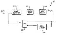
- FIG. 1provides a block diagram of a system 10 for dynamically trimming a VCO 100 .
- the VCO 100receives a trim signal for adjusting a voltage-to-frequency operating characteristic of the VCO 100 , and also receives a tune signal to generate an output signal having an output frequency determined by the voltage-to-frequency operating characteristic.
- the trim circuit 200also receives the tune signal and generates the trim signal in response to the tune signal. Depending on the tune signal, the trim circuit 200 may increment or decrement the trim signal. The change in the trim signal during the increment or decrement is conditioned so that a change in the voltage-to-frequency operating characteristic of the VCO 100 does not exceed a frequency rate change.
- the system 10is implemented in a PLL, and the frequency rate change is defined as a frequency rate tracking capability of the phase locked loop.
- the frequency rate changeis defined as a frequency rate proportional to a bandwidth of the phase locked loop.
- the frequency rate changeis defined as a frequency step proportional to a bandwidth of the phase locked loop.
- the frequency rate changeis defined as a frequency rate at which the PLL may maintain a lock status during the change of the voltage-to-frequency operating characteristic of the VCO 100 .
- FIG. 2proves a more detailed block diagram of the system 10 depicted in FIG. 1.
- the trim circuit 200comprises a trim drive circuit 300 and a trim signal generator 400 .
- the trim drive circuit 300receives the tune signal and generates a trim increment signal (UP) or a trim decrement signal (DN) in response to the tune signal.
- the trim signal generator circuit 400generates the trim signal and increments or decrements the trim signal in response to the trim increment signal and the trim decrement signal generated by the trim drive circuit 300 .
- the trim signal generator 400also conditions a change in the trim signal during the increment or decrement so that a change in the voltage-to-frequency operating characteristic of the VCO 100 does not exceed a frequency rate change.
- FIG. 3provides a block diagram of an illustrative PLL 20 implementing the system 10 for dynamically trimming the VCO 100 . While this illustrative PLL 20 is described with reference to particular circuit components, other PLL implementations may also be used.
- the PLL 20comprises the VCO 100 , a phase detector 120 , a charge pump 130 , a loop filter 140 , and the trim circuit 200 .
- the phase detector 110provides a phase difference between the input signal to the PLL 20 and the output signal of the VCO 100 .
- the charge pump 120charges or discharges the loop filter 130 .
- the loop filter 130provides the tune signal to the VCO 100 and the trim circuit 200 .
- the tune signalis adjusted by the loop filter 130 to maintain lock such that the output frequency F out of the VCO 100 matches the input frequency F in of the input signal.
- the PLL 20can track up to a certain frequency change rate of the input frequency F in .
- the frequency change rateis determined by the particular phase detector 120 , charge pump 130 , and loop filter 140 selected.
- the trim circuit 200can select a number of settings to adjust the voltage-to-frequency operating characteristic of the VCO 100 , and can adjust the voltage-to-frequency operating characteristic of the VCO 100 during operation of the PLL 20 . This allows the VCO 100 center frequency to be trimmed dynamically, even when the PLL 20 is already locked. Furthermore, the PLL 20 implementing the trim circuit 200 exhibits lower sensitivity to noise compared to typical PLLS.
- FIG. 4provides a graph 102 of multiple voltage-to-frequency operating characteristics of the VCO 100 .
- the voltage-to-frequency gain K of the VCO 100may be adjusted to one of a plurality of operating curves K 0 . . . n by the trim input signal.
- an input voltage V tunewhich is provided by the tune signal, generates a corresponding output frequency F out .
- Each operating curvehas a lower voltage limit V L and an upper voltage limit V U that defines an acceptable operational range for the input voltage V tune .
- the input voltage V tuneis at or near the center voltage V c for a selected operating curve K.
- curve Kdepends on the application of the VCO 100 .
- the VCO 100In the PLL 20 , for example, the VCO 100 generates an output signal having a frequency F out that is to remain locked to an input reference signal. Assume initially that the PLL 20 is locked at an output frequency F out equal to F in when the tune signal is at V c . Accordingly, curve K 2 is selected.
- the voltage-to-frequency operating characteristic of the VCO 100may change due to temperature, aging, and other conditions. Therefore, the transfer function of curve K 2 may shift up or down, which in turn will cause the tune signal voltage V tune to shift down or up to maintain lock. If the operating curve K 2 shifts far enough, the loop filter 130 will attempt to drive the tune signal V tune beyond an input limit V U or V L .
- the trim circuit 200increments or decrements the trim signal. This in turn changes the voltage-to-frequency operating characteristic of the VCO 100 so that another curve K is selected. Furthermore, the trim signal is conditioned such that the PLL 20 will maintain lock on the input frequency F in during the change of the voltage-to-frequency operating characteristic.
- the VCO 100drifts from a current operating curve (e.g., K 2 ) to a newly selected operating curve (e.g., K 3 ) at a frequency rate such that the tune signal V tune may be adjusted by the loop filter 130 so that the PLL 20 remains locked during the transition.
- the trim circuit 200 of the PLL 20may also aid in acquiring lock on the input signal by incrementally selecting operating curves K and sweeping the tune signal to acquire a locked state. For example, during initialization of the PLL 20 , the first curve K 0 may be selected to lock to the input frequency F in . Upon failure to lock, the trim circuit 200 will select the next curve, K 1 , and increment through the curves K until a locked state is acquired. As shown in FIG. 2, the PLL 20 eventually acquires a locked state on the curve K 2 . Thereafter, the trim circuit 200 monitors the tune signal as previously described to determine whether to select another curve K. Accordingly, by dynamically trimming the VCO 100 , the trim circuit 200 provides a PLL 20 with greater lock-in range and tracking range than conventional hard- or soft-trimming systems.
- FIG. 5provides a block diagram of one embodiment of the trim circuit 200 for dynamically trimming the VCO 100 .
- the trim drive circuit 300comprises a reference voltage generator 310 and a comparator block 320
- the trim signal generator 400comprises an N-bit counter 410 and a filter bank 420 .
- the reference voltage generator 310creates two reference voltages V U and V L that define a voltage range in which the VCO 100 is properly tunable.
- the comparator block 320comprises a first comparator 322 and a second comparator 324 .
- the reference voltages V U and V Lare provided as input to the inverting input of the first comparator 322 and the noninverting input of the second comparator 324 , respectively.
- the tune signalis provided as input to the noninverting input of the first comparator 322 and the inverting input of the second comparator 324 , respectively.
- the output of the first comparator 322is a trim increment signal (UP), and the output of the second comparator 324 is a trim decrement signal (DN).
- UPtrim increment signal
- DNtrim decrement signal
- the trim drive circuit 300may be realized by other implementations.
- the tune signalmay be provided to an analog-to-digital (A/D) converter to obtain a first digital value.
- the first digital valuemay then be compared to a high digital value and a low digital value to determine whether the tune signal is within acceptable limits. If the first digital value is not within acceptable limits, the corresponding increment or decrement signal is then generated.
- A/Danalog-to-digital
- Other circuit implementations of the trim drive circuitmay also be used.
- the trim increment signal and the trim decrement signalare provided to the trim signal generator 400 .
- the N-bit counter 410produces an N-bit digital value. In one embodiment, only one bit of the N-bit digital value changes during an increment or decrement function.
- the digital value of the N-bit counter 410is filtered through a filter bank 420 .
- the filter bank 420comprises a plurality of low-pass filters each with a time constant ⁇ .
- the output of the filter bank 420comprise trim bits that are provided as the trim signal input to the VCO 100 .
- the quasi-static changeprevents the trim bits input into the VCO 100 from switching on or off suddenly, thus preventing the frequency of the VCO 100 to likewise change suddenly. Such instantaneous frequency steps can result in the PLL 20 losing lock.
- the filterswitches the new trim bit slowly in a quasi-static manner, resulting in a drift of the voltage-to-frequency operating characteristic from a first curve K n to a second curve K n ⁇ 1 .
- the tune voltage V tuneis simultaneously adjusted accordingly to maintain lock.
- the value of the time constant ⁇is determined in part on the loop filter 130 response. Because the PLL 20 can track a certain rate of frequency change, the PLL 20 stays locked in the event of internal VCO frequency drift due to supply or temperature changes. The PLL 20 will remain locked as long as the internal rate of frequency change is slower than the frequency tracking capability of the PLL 20 .
- the choice of the time constant ⁇ and the loop filter 130is also made in such a way to minimize the amount of phase error between the input and the output due to trimming while locked.
- the filter bank 420is omitted.
- the change in the trim bitswill cause a frequency step to occur in the VCO 100 .
- the frequency stepis small compared to the bandwidth of the PLL 20 , then the PLL 20 can track the input signal during the change of the voltage-to-frequency operating characteristic.
- trim signal generator 400The particular implementation of the trim signal generator 400 is illustrative only; the trim signal generator 400 may be realized by other implementations.
- the trim signal generator 400can provide an analog trim signal and condition the change of the analog trim signal such that the change in the voltage-to-frequency operating characteristic of the VCO 100 is not instantaneous.
- FIG. 6provides a block diagram of another embodiment of the trim circuit 200 for dynamically trimming VCO 100 .
- the trim circuit 200comprises a trim drive circuit 300 , a trim signal generator 400 , a control circuit 500 , and a local oscillator (LO) 510 .
- LOlocal oscillator
- the trim signal generator 400comprises a log 2 (N)-bit counter 412 that generates a 2 N binary number, and a log 2 (N)-to-N bit decoder 414 that receives the 2 N binary number and generates an N-bit digital value.
- the log 2 (N)-bit counter 412may be realized by a conventional binary counter that outputs a binary number
- the log 2 (N)-to-N bit decoder 414may be realized by a conventional decoder that decodes a log 2 (N) binary number (i.e., the 2 N binary number) into N bits.
- the log 2 (N)-bit counter 412is a 4-bit counter
- the log 2 (N)-to-N bit decoder 414is a 4:16 bit decoder.
- the output of the log 2 (N)-to-N bit decoder 414is provided to the filter bank 420 to select and change the trim settings on the VCO 100 as described above.
- the control circuit 500receives the trim increment signal and the trim decrement signal from the trim drive circuit 300 and generates a corresponding increment signal (UP) and a corresponding decrement signal (DN), respectively.
- the up signal and down signalcause the log 2 (N)-bit counter 412 to increment or decrement the 2 N binary number, respectively.
- the control circuit 500also aids the PLL 20 in acquiring lock on an input signal.
- the control circuit 500selects an acquisition mode and selectively adjusts the trim signal to adjust the voltage-to-frequency operating characteristic of the VCO 100 during the acquisition mode until the PLL 20 enters a locked state. For example, if the PLL 20 loses lock, or during initialization of the PLL 20 , the first curve K 0 may be selected to lock to the input frequency F in .
- the control circuit 500will select the next curve, K 1 , and increment through the curves K until a locked state is acquired. As shown in FIG. 4, the PLL 20 eventually acquires a locked state on the curve K 2 . Thereafter, the trim circuit 200 monitors the tune signal as previously described to determine whether to adjust the trim signal.
- a local oscillator (LO) 510provides a separate trim clock for the log 2 (N)-bit counter 412 , the log 2 (N)-to-N bit decoder 414 , and the control circuit 500 .
- the control circuit 500comprises synchronous control logic and the LO 510 operates at a clock frequency less than the lowest VCO 100 output frequency.
- the increment or decrement operations of the trim signalare of long enough duration to ensure that the PLL 20 has time to fully shift the VCO 100 to another voltage-to-frequency operating characteristic and determine whether the tune signal is within an acceptable range before the trim signal is changed again.
- the LO 510operates at a frequency within the frequency range of the PLL 20 , or even at a frequency exceeding the frequency range of the PLL 20 .
- the control circuit 500selectively enables and disables the UP and DN signals so that the log 2 (N) bit counter 412 does not increment or decrement so quickly so as to exceed the closed loop response time of the PLL 20 .
- the PLL 20has time to fully shift the VCO 100 to another voltage-to-frequency operating characteristic and determine whether the tune signal is within an acceptable range before the trim signal is changed.
- control circuit 500 and the LO 510provide added stability to the trim circuit 200 by incorporation of hysteresis in the auto-trim control system.
- the ranges of V L , V U , the frequency step each trim bit provides, and the tuning range of the VCO 100are selected as described above to ensure that when the control circuit 500 determines to change the trim signal, the change will shift the voltage-to-frequency operating characteristic and thereby shift the VCO 100 tuning voltage between the V L and V U voltage limits in such a manner that the PLL 20 maintains a locked state. In this manner, oscillation or chattering between two VCO voltage-to-frequency operating characteristics is avoided.
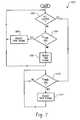
- FIG. 7provides a flow chart 1000 illustrating one process of dynamically trimming the VCO 100 as implemented in FIG. 6, in a PLL 20 .
- the control circuit 500determines whether the PLL 20 is locked. If the PLL 20 is not locked, the control circuit 500 determines whether the tune signal voltage V tune is out of range (OOR) of the voltage range defined by the voltage values V L and V U . If the tune signal voltage V tune is not out of range, the loop filter 130 adjusts the tune signal according to the closed-loop transfer function of the PLL 20 , as shown in step 1006 . Step 1002 is then repeated.
- step 1004if the tune signal voltage V tune is out of range, then the PLL 20 has failed to lock to the input signal for a selected operating curve K. Accordingly, the trim signal is adjusted either up or down, depending on whether the tune signal voltage V tune is less than V L or greater than V U . Step 1002 is then repeated.
- the tune drive circuit 300continuously monitors whether the tune signal voltage V tune is out of range of the voltage range defined by the voltage values V L and V U , as shown in step 1010 . As long as the tune signal voltage V tune is within the voltage range defined by the voltage values V L and V U , the trim signal remains the same. However, once the tune signal voltage V tune is out of the voltage range defined by the voltage values V L and V U , then the trim signal is adjusted either up or down, depending on whether the tune signal voltage V tune is less than V L or greater than V U . After the trim signal is adjusted, the voltage-to-frequency operating characteristic of the VCO 100 will change, as a new operating curve K has been selected. Step 1010 is then again executed, and thus adjustment of the trim signal continues until the tune signal voltage V tune returns to an acceptable voltage range.
- FIG. 8provides another flow chart 1100 illustrating another process of dynamically trimming the VCO 100 as implemented in FIG. 6, in a PLL 20 .
- steps 1002 , 1004 , 1006 , 1008 , 1010 , and 1012 of FIG. 7are similarly executed.
- the trim circuit 200determines whether the tune signal voltage V tune drifts to a center voltage of a newly selected operating curve K. If the tune signal voltage V tune drifts to a center voltage of a newly selected operating curve K, then the optimal operating curve K has been selected.
- the process of selecting the optimal operating curve Kmay be realized by comparing a previous tune signal voltage values to a subsequent tune signal voltage values, and selecting the operating curve K in which a tune signal voltage value is closest to the center voltage V c .
- the process of selecting the optimal operating curve Kmay be realized determining whether the tune signal voltage value is within an acceptable voltage margin centered around the center voltage V c and narrower than the range defined by V L and V U .
- Other processes for selecting the optimal operating curve Kcan also be realized.
- FIGS. 7 and 8are illustrative only; other processes for dynamically adjusting the trim signal of a VCO 100 to acquire lock and to further maintain lock through such adjustments may also be realized.
- a process step similar to step 1014may also be implemented during the acquisition process of steps 1002 - 1008 to ensure that an optimal operating curve K is selected for an initial lock.
- trim circuit 200may also be realized by using, for example, a programmable controller, or an Application Specific Integrated Circuit (ASIC), and the like. Other realizations of the particular functional blocks and corresponding operations, or combinations thereof, may also be used.
- ASICApplication Specific Integrated Circuit
Landscapes
- Stabilization Of Oscillater, Synchronisation, Frequency Synthesizers (AREA)
Abstract
Description
- 1. Field of the Invention[0001]
- The invention relates to oscillators, and more particularly to a system and method for dynamically trimming a voltage controlled oscillator (VCO).[0002]
- 2. Description of the Related Art[0003]
- A VCO is a common circuit component, particularly in a phase locked loop (PLL). A PLL circuit includes a VCO that locks to an incoming reference signal. Generally, the center frequency of the VCO, the VCO gain, and the overall tuning range of the VCO is considered in the design of the PLL.[0004]
- Implementing a VCO in an integrated circuit presents trimming design considerations since the center frequency of the VCO will vary from chip to chip due to the manufacturing process. A typical method of dealing with VCO variations is hard trimming, which utilizes a one-time programmable or selectable center frequency trimming circuit in the VCO. This allows the VCO center frequency to be brought closer to a target frequency. However, with hard trimming, the VCO can only be programmed or trimmed once, and thus the VCO is susceptible to center frequency drifting due to temperature changes, aging, and other effects. To compensate for such effects, the VCO gain is increased; however, this results in a higher sensitivity to noise.[0005]
- Another method of dealing with VCO variations is soft trimming. Soft trimming utilizes a VCO operable to receive a trim signal and adjust a voltage-to-frequency operating characteristic in response to the trim signal, and thus the VCO is less susceptible to center frequency drifting due to temperature changes, aging, and other effects. However, with soft trimming, the circuit implementing the VCO usually trims during a non-operational state, e.g., a calibration state, or often suffers from temporary system degradation during soft trimming, e.g., the PLL may temporarily lose lock during the trimming adjustment.[0006]
- A system is provided for dynamically trimming a voltage controlled oscillator operable to receive a trim signal for adjusting a voltage-to-frequency operating characteristic of the voltage controlled oscillator and receive a tune signal to generate an output signal having an output frequency determined by the voltage-to-frequency operating characteristic. The system comprises a trim circuit operable to receive the tune signal and generate the trim signal in response to the tune signal and increment or decrement the trim signal and condition a change in the trim signal during the increment or decrement so that the voltage-to-frequency operating characteristic of the voltage controlled oscillator drifts from a first voltage-to-frequency operating characteristic to a second voltage-to-frequency operating characteristic at a rate less than a specified frequency rate.[0007]
- A phase locked loop comprises a voltage controlled oscillator, a loop filter and a trim circuit. The voltage controlled oscillator is operable to receive a trim signal for adjusting a voltage-to-frequency operating characteristic of the voltage controlled oscillator, and receive a tune signal to generate an output signal having an output frequency determined by the voltage-to-frequency operating characteristic. The loop filter is operable to receive an error signal and generate the tune signal in response to the error signal. The trim circuit is operable to receive the tune signal and generate the trim signal and increment or decrement the trim signal and condition a change in the trim signal during the increment or decrement so that the voltage-to-frequency operating characteristic of the voltage controlled oscillator drifts from a first voltage-to-frequency operating characteristic to a second voltage-to-frequency operating characteristic at a rate at which the phase locked loop remains in a locked state.[0008]
- A method of dynamically trimming a voltage controlled oscillator in a phase locked loop comprises the steps of determining if a voltage-to-frequency operating characteristic of the voltage controlled oscillator needs adjustment; generating a trim control signal to adjust the voltage-to-frequency operating characteristic of the voltage controlled oscillator upon a positive determination; and conditioning the generation of the trim control signal so that the rate of change of the voltage-to-frequency operating characteristic of the voltage controlled oscillator is controlled so that the phase locked loop remains in a locked state during adjustment of the voltage-to-frequency operating characteristic of the voltage controlled oscillator.[0009]
- FIG. 1 is a block diagram of a system for dynamically trimming a VCO;[0010]
- FIG. 2 is a more detailed block diagram of the system depicted in FIG. 1;[0011]
- FIG. 3 is a block diagram of a PLL implementing the system for dynamically trimming a VCO;[0012]
- FIG. 4 is a graph of multiple voltage-to-frequency operating characteristics of a VCO;[0013]
- FIG. 5 is a block diagram of one embodiment of a trim circuit for dynamically trimming a VCO;[0014]
- FIG. 6 is a block diagram of another embodiment of the trim circuit for dynamically trimming VCO;[0015]
- FIG. 7 is a flow chart illustrating one process of dynamically trimming the VCO of the PLL of FIG. 6; and[0016]
- FIG. 8 is a flow chart illustrating another process of dynamically trimming the VCO of the PLL of FIG. 6.[0017]
- Throughout the drawings, the same or similar reference numerals are applied to the same or similar parts, elements and steps, and thus the description of the same or similar parts, elements and steps will be omitted or simplified when possible.[0018]
- FIG. 1 provides a block diagram of a[0019]
system 10 for dynamically trimming aVCO 100. TheVCO 100 receives a trim signal for adjusting a voltage-to-frequency operating characteristic of theVCO 100, and also receives a tune signal to generate an output signal having an output frequency determined by the voltage-to-frequency operating characteristic. - The[0020]
trim circuit 200 also receives the tune signal and generates the trim signal in response to the tune signal. Depending on the tune signal, thetrim circuit 200 may increment or decrement the trim signal. The change in the trim signal during the increment or decrement is conditioned so that a change in the voltage-to-frequency operating characteristic of theVCO 100 does not exceed a frequency rate change. - In one embodiment, the[0021]
system 10 is implemented in a PLL, and the frequency rate change is defined as a frequency rate tracking capability of the phase locked loop. In another embodiment, the frequency rate change is defined as a frequency rate proportional to a bandwidth of the phase locked loop. In yet another embodiment, the frequency rate change is defined as a frequency step proportional to a bandwidth of the phase locked loop. And in yet another embodiment, the frequency rate change is defined as a frequency rate at which the PLL may maintain a lock status during the change of the voltage-to-frequency operating characteristic of theVCO 100. - FIG. 2 proves a more detailed block diagram of the[0022]
system 10 depicted in FIG. 1. Thetrim circuit 200 comprises atrim drive circuit 300 and atrim signal generator 400. Thetrim drive circuit 300 receives the tune signal and generates a trim increment signal (UP) or a trim decrement signal (DN) in response to the tune signal. The trimsignal generator circuit 400 generates the trim signal and increments or decrements the trim signal in response to the trim increment signal and the trim decrement signal generated by thetrim drive circuit 300. Thetrim signal generator 400 also conditions a change in the trim signal during the increment or decrement so that a change in the voltage-to-frequency operating characteristic of theVCO 100 does not exceed a frequency rate change. - FIG. 3 provides a block diagram of an[0023]
illustrative PLL 20 implementing thesystem 10 for dynamically trimming theVCO 100. While thisillustrative PLL 20 is described with reference to particular circuit components, other PLL implementations may also be used. ThePLL 20 comprises theVCO 100, aphase detector 120, acharge pump 130, a loop filter140, and thetrim circuit 200. Thephase detector 110 provides a phase difference between the input signal to thePLL 20 and the output signal of theVCO 100. The charge pump120 charges or discharges theloop filter 130. Theloop filter 130 provides the tune signal to theVCO 100 and thetrim circuit 200. The tune signal is adjusted by theloop filter 130 to maintain lock such that the output frequency Foutof theVCO 100 matches the input frequency Finof the input signal. ThePLL 20 can track up to a certain frequency change rate of the input frequency Fin. The frequency change rate is determined by theparticular phase detector 120,charge pump 130, and loop filter140 selected. - The[0024]
trim circuit 200 can select a number of settings to adjust the voltage-to-frequency operating characteristic of theVCO 100, and can adjust the voltage-to-frequency operating characteristic of theVCO 100 during operation of thePLL 20. This allows the VCO100 center frequency to be trimmed dynamically, even when thePLL 20 is already locked. Furthermore, thePLL 20 implementing thetrim circuit 200 exhibits lower sensitivity to noise compared to typical PLLS. - FIG. 4 provides a[0025]
graph 102 of multiple voltage-to-frequency operating characteristics of theVCO 100. The voltage-to-frequency gain K of theVCO 100 may be adjusted to one of a plurality of operating curves K0 . . . nby the trim input signal. For each operating curve K, an input voltage Vtune, which is provided by the tune signal, generates a corresponding output frequency Fout. Each operating curve has a lower voltage limit VLand an upper voltage limit VUthat defines an acceptable operational range for the input voltage Vtune. During ideal operation, the input voltage Vtuneis at or near the center voltage Vcfor a selected operating curve K. - Selection of a particular curve K depends on the application of the[0026]
VCO 100. In thePLL 20, for example, theVCO 100 generates an output signal having a frequency Foutthat is to remain locked to an input reference signal. Assume initially that thePLL 20 is locked at an output frequency Foutequal to Finwhen the tune signal is at Vc. Accordingly, curve K2is selected. During operation of thePLL 20, however, the voltage-to-frequency operating characteristic of theVCO 100 may change due to temperature, aging, and other conditions. Therefore, the transfer function of curve K2may shift up or down, which in turn will cause the tune signal voltage Vtuneto shift down or up to maintain lock. If the operating curve K2shifts far enough, theloop filter 130 will attempt to drive the tune signal Vtunebeyond an input limit VUor VL. - When the tune signal exceeds one of the threshold voltages V[0027]Uor VL, the
trim circuit 200 increments or decrements the trim signal. This in turn changes the voltage-to-frequency operating characteristic of theVCO 100 so that another curve K is selected. Furthermore, the trim signal is conditioned such that thePLL 20 will maintain lock on the input frequency Finduring the change of the voltage-to-frequency operating characteristic. In one embodiment, theVCO 100 drifts from a current operating curve (e.g., K2) to a newly selected operating curve (e.g., K3) at a frequency rate such that the tune signal Vtunemay be adjusted by theloop filter 130 so that thePLL 20 remains locked during the transition. - The[0028]
trim circuit 200 of thePLL 20 may also aid in acquiring lock on the input signal by incrementally selecting operating curves K and sweeping the tune signal to acquire a locked state. For example, during initialization of thePLL 20, the first curve K0may be selected to lock to the input frequency Fin. Upon failure to lock, thetrim circuit 200 will select the next curve, K1, and increment through the curves K until a locked state is acquired. As shown in FIG. 2, thePLL 20 eventually acquires a locked state on the curve K2. Thereafter, thetrim circuit 200 monitors the tune signal as previously described to determine whether to select another curve K. Accordingly, by dynamically trimming theVCO 100, thetrim circuit 200 provides aPLL 20 with greater lock-in range and tracking range than conventional hard- or soft-trimming systems. - FIG. 5 provides a block diagram of one embodiment of the[0029]
trim circuit 200 for dynamically trimming theVCO 100. Thetrim drive circuit 300 comprises areference voltage generator 310 and acomparator block 320, and thetrim signal generator 400 comprises an N-bit counter 410 and afilter bank 420. - The[0030]
reference voltage generator 310 creates two reference voltages VUand VLthat define a voltage range in which theVCO 100 is properly tunable. Thecomparator block 320 comprises afirst comparator 322 and asecond comparator 324. The reference voltages VUand VLare provided as input to the inverting input of thefirst comparator 322 and the noninverting input of thesecond comparator 324, respectively. Furthermore, the tune signal is provided as input to the noninverting input of thefirst comparator 322 and the inverting input of thesecond comparator 324, respectively. The output of thefirst comparator 322 is a trim increment signal (UP), and the output of thesecond comparator 324 is a trim decrement signal (DN). Thus, when the tune signal is greater than the reference voltage VU, the trim increment signal goes high; likewise, when the tune signal is less than the reference voltage VL, the trim decrement signal goes high. - The particular implementation of the[0031]
trim drive circuit 300 is illustrative only; thetrim drive circuit 300 may be realized by other implementations. For example, the tune signal may be provided to an analog-to-digital (A/D) converter to obtain a first digital value. The first digital value may then be compared to a high digital value and a low digital value to determine whether the tune signal is within acceptable limits. If the first digital value is not within acceptable limits, the corresponding increment or decrement signal is then generated. Other circuit implementations of the trim drive circuit may also be used. - The trim increment signal and the trim decrement signal are provided to the[0032]
trim signal generator 400. The N-bit counter 410 produces an N-bit digital value. In one embodiment, only one bit of the N-bit digital value changes during an increment or decrement function. The digital value of the N-bit counter 410 is filtered through afilter bank 420. In one embodiment, thefilter bank 420 comprises a plurality of low-pass filters each with a time constant τ. The output of thefilter bank 420 comprise trim bits that are provided as the trim signal input to theVCO 100. - The[0033]
filter bank 420 causes the bits in the trim signal to change slowly in a quasi-static manner. For example, if thefilter bank 420 comprises a plurality of single pole RC filters, then the bits in the trim signal will change according to the time constant τ=RC. The quasi-static change prevents the trim bits input into theVCO 100 from switching on or off suddenly, thus preventing the frequency of theVCO 100 to likewise change suddenly. Such instantaneous frequency steps can result in thePLL 20 losing lock. However, when a trim bit is filtered through thefilter bank 420, the filter switches the new trim bit slowly in a quasi-static manner, resulting in a drift of the voltage-to-frequency operating characteristic from a first curve Knto a second curve Kn±1. The tune voltage Vtuneis simultaneously adjusted accordingly to maintain lock. - The value of the time constant τ is determined in part on the[0034]
loop filter 130 response. Because thePLL 20 can track a certain rate of frequency change, thePLL 20 stays locked in the event of internal VCO frequency drift due to supply or temperature changes. ThePLL 20 will remain locked as long as the internal rate of frequency change is slower than the frequency tracking capability of thePLL 20. The choice of the time constant τ and theloop filter 130 is also made in such a way to minimize the amount of phase error between the input and the output due to trimming while locked. - In another embodiment, the[0035]
filter bank 420 is omitted. In this embodiment, the change in the trim bits will cause a frequency step to occur in theVCO 100. However, if the frequency step is small compared to the bandwidth of thePLL 20, then thePLL 20 can track the input signal during the change of the voltage-to-frequency operating characteristic. - The particular implementation of the[0036]
trim signal generator 400 is illustrative only; thetrim signal generator 400 may be realized by other implementations. For example, if theVCO 100 is operable to receive an analog trim signal, thetrim signal generator 400 can provide an analog trim signal and condition the change of the analog trim signal such that the change in the voltage-to-frequency operating characteristic of theVCO 100 is not instantaneous. - FIG. 6 provides a block diagram of another embodiment of the[0037]
trim circuit 200 for dynamically trimmingVCO 100. Thetrim circuit 200 comprises atrim drive circuit 300, atrim signal generator 400, acontrol circuit 500, and a local oscillator (LO)510. - In this embodiment, the[0038]
trim signal generator 400 comprises a log2(N)-bit counter 412 that generates a 2Nbinary number, and a log2(N)-to-N bit decoder 414 that receives the 2Nbinary number and generates an N-bit digital value. The log2(N)-bit counter 412 may be realized by a conventional binary counter that outputs a binary number, and the log2(N)-to-N bit decoder 414 may be realized by a conventional decoder that decodes a log2(N) binary number (i.e., the 2Nbinary number) into N bits. In one embodiment, the log2(N)-bit counter 412 is a 4-bit counter, and the log2(N)-to-N bit decoder 414 is a 4:16 bit decoder. The output of the log2(N)-to-N bit decoder 414 is provided to thefilter bank 420 to select and change the trim settings on theVCO 100 as described above. - When the[0039]
PLL 20 is locked, thecontrol circuit 500 receives the trim increment signal and the trim decrement signal from thetrim drive circuit 300 and generates a corresponding increment signal (UP) and a corresponding decrement signal (DN), respectively. The up signal and down signal cause the log2(N)-bit counter 412 to increment or decrement the 2Nbinary number, respectively. - The[0040]
control circuit 500 also aids thePLL 20 in acquiring lock on an input signal. When thePLL 20 is not locked, thecontrol circuit 500 selects an acquisition mode and selectively adjusts the trim signal to adjust the voltage-to-frequency operating characteristic of theVCO 100 during the acquisition mode until thePLL 20 enters a locked state. For example, if thePLL 20 loses lock, or during initialization of thePLL 20, the first curve K0may be selected to lock to the input frequency Fin. Upon failure to lock, thecontrol circuit 500 will select the next curve, K1, and increment through the curves K until a locked state is acquired. As shown in FIG. 4, thePLL 20 eventually acquires a locked state on the curve K2. Thereafter, thetrim circuit 200 monitors the tune signal as previously described to determine whether to adjust the trim signal. - A local oscillator (LO)[0041]510 provides a separate trim clock for the log2(N)-
bit counter 412, the log2(N)-to-N bit decoder 414, and thecontrol circuit 500. In one embodiment, thecontrol circuit 500 comprises synchronous control logic and theLO 510 operates at a clock frequency less than thelowest VCO 100 output frequency. By driving the log2(N)-bit counter 412, the log2(N)-to-N bit decoder 414, and thecontrol circuit 500 at a frequency lower than the lowest operating frequency of theVCO 100, the increment or decrement operations of the trim signal are of long enough duration to ensure that thePLL 20 has time to fully shift theVCO 100 to another voltage-to-frequency operating characteristic and determine whether the tune signal is within an acceptable range before the trim signal is changed again. - Other operating frequencies for the[0042]
LO 510 may also be selected. In another embodiment, theLO 510 operates at a frequency within the frequency range of thePLL 20, or even at a frequency exceeding the frequency range of thePLL 20. In this embodiment, thecontrol circuit 500 selectively enables and disables the UP and DN signals so that the log2(N) bit counter412 does not increment or decrement so quickly so as to exceed the closed loop response time of thePLL 20. Thus, thePLL 20 has time to fully shift theVCO 100 to another voltage-to-frequency operating characteristic and determine whether the tune signal is within an acceptable range before the trim signal is changed. - Thus, the[0043]
control circuit 500 and theLO 510 provide added stability to thetrim circuit 200 by incorporation of hysteresis in the auto-trim control system. The ranges of VL, VU, the frequency step each trim bit provides, and the tuning range of theVCO 100 are selected as described above to ensure that when thecontrol circuit 500 determines to change the trim signal, the change will shift the voltage-to-frequency operating characteristic and thereby shift theVCO 100 tuning voltage between the VLand VUvoltage limits in such a manner that thePLL 20 maintains a locked state. In this manner, oscillation or chattering between two VCO voltage-to-frequency operating characteristics is avoided. - FIG. 7 provides a[0044]
flow chart 1000 illustrating one process of dynamically trimming theVCO 100 as implemented in FIG. 6, in aPLL 20. Instep 1002, thecontrol circuit 500 determines whether thePLL 20 is locked. If thePLL 20 is not locked, thecontrol circuit 500 determines whether the tune signal voltage Vtuneis out of range (OOR) of the voltage range defined by the voltage values VLand VU. If the tune signal voltage Vtuneis not out of range, theloop filter 130 adjusts the tune signal according to the closed-loop transfer function of thePLL 20, as shown instep 1006.Step 1002 is then repeated. - Returning to step[0045]1004, if the tune signal voltage Vtuneis out of range, then the
PLL 20 has failed to lock to the input signal for a selected operating curve K. Accordingly, the trim signal is adjusted either up or down, depending on whether the tune signal voltage Vtuneis less than VLor greater than VU. Step1002 is then repeated. - Once the[0046]
PLL 20 acquires lock, then thetune drive circuit 300 continuously monitors whether the tune signal voltage Vtuneis out of range of the voltage range defined by the voltage values VLand VU, as shown instep 1010. As long as the tune signal voltage Vtuneis within the voltage range defined by the voltage values VLand VU, the trim signal remains the same. However, once the tune signal voltage Vtuneis out of the voltage range defined by the voltage values VLand VU, then the trim signal is adjusted either up or down, depending on whether the tune signal voltage Vtuneis less than VLor greater than VU. After the trim signal is adjusted, the voltage-to-frequency operating characteristic of theVCO 100 will change, as a new operating curve K has been selected.Step 1010 is then again executed, and thus adjustment of the trim signal continues until the tune signal voltage Vtunereturns to an acceptable voltage range. - FIG. 8 provides another[0047]
flow chart 1100 illustrating another process of dynamically trimming theVCO 100 as implemented in FIG. 6, in aPLL 20. In this process, steps1002,1004,1006,1008,1010, and1012 of FIG. 7 are similarly executed. However, afterstep 1012, thetrim circuit 200 determines whether the tune signal voltage Vtunedrifts to a center voltage of a newly selected operating curve K. If the tune signal voltage Vtunedrifts to a center voltage of a newly selected operating curve K, then the optimal operating curve K has been selected. - Conversely, if the tune signal voltage V[0048]tunedoes not drift near a center voltage of a newly selected operating curve K, then the optimal operating curve K has not been selected. Accordingly, steps1012 and1014 are repeated. Through repeated attempts, the operating curve K in which the tune signal voltage Vtunedrifts closest to the center voltage Vcis eventually selected.
- The process of selecting the optimal operating curve K may be realized by comparing a previous tune signal voltage values to a subsequent tune signal voltage values, and selecting the operating curve K in which a tune signal voltage value is closest to the center voltage V[0049]c. Alternatively, the process of selecting the optimal operating curve K may be realized determining whether the tune signal voltage value is within an acceptable voltage margin centered around the center voltage Vcand narrower than the range defined by VLand VU. Other processes for selecting the optimal operating curve K can also be realized.
- The processes of FIGS. 7 and 8 are illustrative only; other processes for dynamically adjusting the trim signal of a[0050]
VCO 100 to acquire lock and to further maintain lock through such adjustments may also be realized. For example, a process step similar to step1014 may also be implemented during the acquisition process of steps1002-1008 to ensure that an optimal operating curve K is selected for an initial lock. - The embodiments described above are illustrative only. For example, while the embodiments are illustratively realized using discrete components, the[0051]
trim circuit 200 may also be realized by using, for example, a programmable controller, or an Application Specific Integrated Circuit (ASIC), and the like. Other realizations of the particular functional blocks and corresponding operations, or combinations thereof, may also be used. - The embodiments described herein are examples of structures, systems or methods having elements corresponding to the elements of the invention recited in the claims. This written description may enable those of ordinary skill in the art to make and use embodiments having alternative elements that likewise correspond to the elements of the invention received in the claims. The intended scope of the invention thus includes other structures, systems or methods that do not differ from the literal language of the claims, and further includes other structures, systems or methods with insubstantial differences from the literal language of the claims.[0052]
Claims (42)
Priority Applications (3)
| Application Number | Priority Date | Filing Date | Title |
|---|---|---|---|
| US10/294,307US6778024B2 (en) | 2002-11-14 | 2002-11-14 | Dynamically trimmed voltage controlled oscillator |
| AU2003281886AAU2003281886A1 (en) | 2002-11-14 | 2003-11-10 | Dynamically trimmed voltage controlled oscillator |
| PCT/CA2003/001729WO2004045077A1 (en) | 2002-11-14 | 2003-11-10 | Dynamically trimmed voltage controlled oscillator |
Applications Claiming Priority (1)
| Application Number | Priority Date | Filing Date | Title |
|---|---|---|---|
| US10/294,307US6778024B2 (en) | 2002-11-14 | 2002-11-14 | Dynamically trimmed voltage controlled oscillator |
Publications (2)
| Publication Number | Publication Date |
|---|---|
| US20040095194A1true US20040095194A1 (en) | 2004-05-20 |
| US6778024B2 US6778024B2 (en) | 2004-08-17 |
Family
ID=32296955
Family Applications (1)
| Application Number | Title | Priority Date | Filing Date |
|---|---|---|---|
| US10/294,307Expired - Fee RelatedUS6778024B2 (en) | 2002-11-14 | 2002-11-14 | Dynamically trimmed voltage controlled oscillator |
Country Status (3)
| Country | Link |
|---|---|
| US (1) | US6778024B2 (en) |
| AU (1) | AU2003281886A1 (en) |
| WO (1) | WO2004045077A1 (en) |
Cited By (5)
| Publication number | Priority date | Publication date | Assignee | Title |
|---|---|---|---|---|
| US20040201939A1 (en)* | 2002-12-02 | 2004-10-14 | Silverbrook Research Pty Ltd | Clock trim mechanism for onboard system clock |
| EP1670136A1 (en)* | 2004-12-13 | 2006-06-14 | Infineon Technologies AG | Voltage controlled oscillator with analogue and digital control |
| US20070286321A1 (en)* | 2006-06-13 | 2007-12-13 | Gupta Atul K | Linear sample and hold phase detector for clocking circuits |
| US20090319802A1 (en)* | 2002-12-02 | 2009-12-24 | Silverbrook Research Pty Ltd | Key Genaration In An Integrated Circuit |
| CN109245724A (en)* | 2018-07-24 | 2019-01-18 | 北京时代民芯科技有限公司 | A kind of adaptive-biased broadband voltage controlled pierce circuit |
Families Citing this family (12)
| Publication number | Priority date | Publication date | Assignee | Title |
|---|---|---|---|---|
| US7738618B2 (en)* | 2003-10-23 | 2010-06-15 | Telefonaktiebolaget L M Ericsson (Publ) | Multiband PLL arrangement and a method of controlling such arrangement |
| US7047146B2 (en)* | 2003-12-19 | 2006-05-16 | Airoha Technology Corp | Method for automatically calibrating the frequency range of a PLL and associated PLL capable of automatic calibration |
| US7129800B2 (en)* | 2004-02-04 | 2006-10-31 | Sun Microsystems, Inc. | Compensation technique to mitigate aging effects in integrated circuit components |
| US6949981B2 (en)* | 2004-02-18 | 2005-09-27 | International Business Machines Corporation | Dynamic threshold for VCO calibration |
| US7236034B2 (en)* | 2004-07-27 | 2007-06-26 | Texas Instruments Incorporated | Self correcting scheme to match pull up and pull down devices |
| US7338817B2 (en)* | 2005-03-31 | 2008-03-04 | Intel Corporation | Body bias compensation for aged transistors |
| US20090188549A1 (en)* | 2008-01-29 | 2009-07-30 | Mtvp Corporation | Method of and apparatus for improved thermophotonic generation of electricity |
| US7683685B2 (en) | 2008-02-05 | 2010-03-23 | Sony Corporation | System and method for implementing a digital phase-locked loop |
| TW200935719A (en)* | 2008-02-05 | 2009-08-16 | Rafael Microelectronics Inc | Multi-band VCO |
| ITTO20130347A1 (en) | 2013-04-29 | 2014-10-30 | St Microelectronics Srl | CIRCUIT AND CALIBRATION METHOD FOR A DIGITALLY CONTROLLED OSCILLATOR |
| US9030241B2 (en)* | 2013-04-30 | 2015-05-12 | Micrel, Inc. | PLL frequency synthesizer with multi-curve VCO implementing closed loop curve searching |
| US8872556B1 (en) | 2013-04-30 | 2014-10-28 | Micrel, Inc. | PLL frequency synthesizer with multi-curve VCO implementing closed loop curve searching using charge pump current modulation |
Citations (10)
| Publication number | Priority date | Publication date | Assignee | Title |
|---|---|---|---|---|
| US4726022A (en)* | 1986-04-30 | 1988-02-16 | International Business Machines Corporation | Method and apparatus for stressing the data window in magnetic storage devices |
| US4929918A (en)* | 1989-06-07 | 1990-05-29 | International Business Machines Corporation | Setting and dynamically adjusting VCO free-running frequency at system level |
| US5625325A (en)* | 1995-12-22 | 1997-04-29 | Microtune, Inc. | System and method for phase lock loop gain stabilization |
| US5648744A (en)* | 1995-12-22 | 1997-07-15 | Microtune, Inc. | System and method for voltage controlled oscillator automatic band selection |
| US5686864A (en)* | 1995-09-05 | 1997-11-11 | Motorola, Inc. | Method and apparatus for controlling a voltage controlled oscillator tuning range in a frequency synthesizer |
| US5736904A (en)* | 1996-12-02 | 1998-04-07 | Motorola, Inc. | Automatic trimming of a controlled oscillator in a phase locked loop |
| US5942949A (en)* | 1997-10-14 | 1999-08-24 | Lucent Technologies Inc. | Self-calibrating phase-lock loop with auto-trim operations for selecting an appropriate oscillator operating curve |
| US6091304A (en)* | 1998-09-22 | 2000-07-18 | Lg Information & Communications, Ltd. | Frequency band select phase lock loop device |
| US6133797A (en)* | 1999-07-30 | 2000-10-17 | Motorola, Inc. | Self calibrating VCO correction circuit and method of operation |
| US6172579B1 (en)* | 1999-02-02 | 2001-01-09 | Cleveland Medical Devices Inc. | Three point modulated phase locked loop frequency synthesis system and method |
Family Cites Families (5)
| Publication number | Priority date | Publication date | Assignee | Title |
|---|---|---|---|---|
| GB2120478B (en) | 1982-04-22 | 1985-10-16 | Standard Telephones Cables Ltd | Voltage controlled oscillator |
| CA2112290C (en) | 1993-12-23 | 2004-06-01 | John R. Francis | A clock recovery circuit for serial digital video |
| EP1193875B1 (en) | 2000-09-15 | 2005-11-09 | Alcatel | Voltage-controlled oscillator with automatic center frequency calibration |
| EP1189347A1 (en) | 2000-09-15 | 2002-03-20 | Texas Instruments France | Electronically trimmed VCO |
| US6552618B2 (en) | 2000-12-13 | 2003-04-22 | Agere Systems Inc. | VCO gain self-calibration for low voltage phase lock-loop applications |
- 2002
- 2002-11-14USUS10/294,307patent/US6778024B2/ennot_activeExpired - Fee Related
- 2003
- 2003-11-10WOPCT/CA2003/001729patent/WO2004045077A1/ennot_activeApplication Discontinuation
- 2003-11-10AUAU2003281886Apatent/AU2003281886A1/ennot_activeAbandoned
Patent Citations (11)
| Publication number | Priority date | Publication date | Assignee | Title |
|---|---|---|---|---|
| US4726022A (en)* | 1986-04-30 | 1988-02-16 | International Business Machines Corporation | Method and apparatus for stressing the data window in magnetic storage devices |
| US4929918A (en)* | 1989-06-07 | 1990-05-29 | International Business Machines Corporation | Setting and dynamically adjusting VCO free-running frequency at system level |
| US5686864A (en)* | 1995-09-05 | 1997-11-11 | Motorola, Inc. | Method and apparatus for controlling a voltage controlled oscillator tuning range in a frequency synthesizer |
| US5625325A (en)* | 1995-12-22 | 1997-04-29 | Microtune, Inc. | System and method for phase lock loop gain stabilization |
| US5648744A (en)* | 1995-12-22 | 1997-07-15 | Microtune, Inc. | System and method for voltage controlled oscillator automatic band selection |
| US5736904A (en)* | 1996-12-02 | 1998-04-07 | Motorola, Inc. | Automatic trimming of a controlled oscillator in a phase locked loop |
| US5942949A (en)* | 1997-10-14 | 1999-08-24 | Lucent Technologies Inc. | Self-calibrating phase-lock loop with auto-trim operations for selecting an appropriate oscillator operating curve |
| US6114920A (en)* | 1997-10-14 | 2000-09-05 | Lucent Technologies Inc. | Self-calibrating voltage-controlled oscillator for asynchronous phase applications |
| US6091304A (en)* | 1998-09-22 | 2000-07-18 | Lg Information & Communications, Ltd. | Frequency band select phase lock loop device |
| US6172579B1 (en)* | 1999-02-02 | 2001-01-09 | Cleveland Medical Devices Inc. | Three point modulated phase locked loop frequency synthesis system and method |
| US6133797A (en)* | 1999-07-30 | 2000-10-17 | Motorola, Inc. | Self calibrating VCO correction circuit and method of operation |
Cited By (25)
| Publication number | Priority date | Publication date | Assignee | Title |
|---|---|---|---|---|
| US20080155826A1 (en)* | 2002-12-02 | 2008-07-03 | Silverbrook Research Pty Ltd | Method of manufacturing mems ics |
| US20100223453A1 (en)* | 2002-12-02 | 2010-09-02 | Silverbrook Research Pty Ltd | Integrated circuit for validating and decrypting software data |
| US8038239B2 (en) | 2002-12-02 | 2011-10-18 | Silverbrook Research Pty Ltd | Controller for printhead having arbitrarily joined nozzle rows |
| US8005636B2 (en)* | 2002-12-02 | 2011-08-23 | Silverbrook Research Pty Ltd | Method of controlling clock signal |
| US7096137B2 (en)* | 2002-12-02 | 2006-08-22 | Silverbrook Research Pty Ltd | Clock trim mechanism for onboard system clock |
| US20060259258A1 (en)* | 2002-12-02 | 2006-11-16 | Silverbrook Research Pty Ltd | Quality assurance IC having clock trimmer |
| US7171323B2 (en)* | 2002-12-02 | 2007-01-30 | Silverbrook Research Pty Ltd | Integrated circuit having clock trim circuitry |
| US20090058903A1 (en)* | 2002-12-02 | 2009-03-05 | Silverbrook Research Pty Ltd. | Printer controller configured to compensate for dead printhead nozzles |
| US20100238213A1 (en)* | 2002-12-02 | 2010-09-23 | Silverbrook Research Pty Ltd | Method for dead nozzle remapping |
| US7328115B2 (en)* | 2002-12-02 | 2008-02-05 | Silverbrook Research Pty Ltd | Quality assurance IC having clock trimmer |
| US20080086655A1 (en)* | 2002-12-02 | 2008-04-10 | Silverbrook Research Pty Ltd | Method Of Controlling Quality For A Print Controller |
| US20080150997A1 (en)* | 2002-12-02 | 2008-06-26 | Silverbrook Research Pty Ltd | Method Of Manufacturing Printhead ICS Incorporating Mems Inkjet Nozzles |
| US20060052962A1 (en)* | 2002-12-02 | 2006-03-09 | Silverbrook Research Pty Ltd. | Integrated circuit having clock trim circuitry |
| US7976116B2 (en) | 2002-12-02 | 2011-07-12 | Silverbrook Research Pty Ltd | Inkjet printer system having equalised control of different nozzle count printhead ICs |
| US20040201939A1 (en)* | 2002-12-02 | 2004-10-14 | Silverbrook Research Pty Ltd | Clock trim mechanism for onboard system clock |
| US20090319802A1 (en)* | 2002-12-02 | 2009-12-24 | Silverbrook Research Pty Ltd | Key Genaration In An Integrated Circuit |
| US20100010767A1 (en)* | 2002-12-02 | 2010-01-14 | Silverbrook Research Pty Ltd | Method Of Controlling Clock Signal |
| US20100039467A1 (en)* | 2002-12-02 | 2010-02-18 | Silverbrook Research Pty Ltd | Inkjet printer system having equalised control of different nozzle count printhead ics |
| US7610163B2 (en)* | 2002-12-02 | 2009-10-27 | Silverbrook Research Pty Ltd | Method of controlling quality for a print controller |
| US7301411B2 (en) | 2004-12-13 | 2007-11-27 | Infineon Technologies Ag | Voltage-controlled oscillator circuit with analogue and digital actuation |
| US20060152292A1 (en)* | 2004-12-13 | 2006-07-13 | Infineon Technologies Ag. | Voltage-controlled oscillator circuit with analogue and digital actuation |
| EP1670136A1 (en)* | 2004-12-13 | 2006-06-14 | Infineon Technologies AG | Voltage controlled oscillator with analogue and digital control |
| US7764759B2 (en)* | 2006-06-13 | 2010-07-27 | Gennum Corporation | Linear sample and hold phase detector for clocking circuits |
| US20070286321A1 (en)* | 2006-06-13 | 2007-12-13 | Gupta Atul K | Linear sample and hold phase detector for clocking circuits |
| CN109245724A (en)* | 2018-07-24 | 2019-01-18 | 北京时代民芯科技有限公司 | A kind of adaptive-biased broadband voltage controlled pierce circuit |
Also Published As
| Publication number | Publication date |
|---|---|
| WO2004045077A1 (en) | 2004-05-27 |
| AU2003281886A1 (en) | 2004-06-03 |
| US6778024B2 (en) | 2004-08-17 |
Similar Documents
| Publication | Publication Date | Title |
|---|---|---|
| US6778024B2 (en) | Dynamically trimmed voltage controlled oscillator | |
| US6747519B2 (en) | Phase-locked loop with automatic frequency tuning | |
| US6552618B2 (en) | VCO gain self-calibration for low voltage phase lock-loop applications | |
| US7519140B2 (en) | Automatic frequency correction PLL circuit | |
| EP0669722B1 (en) | PLL circuit having shortened locking time | |
| US7408419B2 (en) | Sigma-delta fractional-N PLL with reduced frequency error | |
| JP3254427B2 (en) | VCO characteristic calibration method | |
| US6704381B1 (en) | Frequency acquisition rate control in phase lock loop circuits | |
| JP2000183734A (en) | Phase rock dollar | |
| US6927611B2 (en) | Semidigital delay-locked loop using an analog-based finite state machine | |
| US7548124B2 (en) | System and method for self calibrating voltage-controlled oscillator | |
| US7711340B2 (en) | Phase locked loop and method thereof | |
| EP1518325A1 (en) | Phase-locked loop with automatic frequency tuning | |
| US6774732B1 (en) | System and method for coarse tuning a phase locked loop (PLL) synthesizer using 2-PI slip detection | |
| US6351164B1 (en) | PLL circuit | |
| US7738618B2 (en) | Multiband PLL arrangement and a method of controlling such arrangement | |
| US6545545B1 (en) | Voltage-controlled oscillator frequency auto-calibrating system | |
| US20070018745A1 (en) | Establishing a tuning signal window for use in centering a multi-band voltage controlled oscillator | |
| US6411144B1 (en) | Phase-locked loop circuit | |
| JP2842847B2 (en) | PLL synthesizer circuit | |
| US7408415B2 (en) | Voltage controlled oscillator phase locked loop circuit with loop filter capacitance tuning | |
| US7548126B2 (en) | Phase locked loop circuit and control method thereof | |
| WO2004015869A1 (en) | Phase-locked-loop circuit and method |
Legal Events
| Date | Code | Title | Description |
|---|---|---|---|
| AS | Assignment | Owner name:GENNUM CORPORATION, CANADA Free format text:ASSIGNMENT OF ASSIGNORS INTEREST;ASSIGNORS:GUPTA, ATUL K.;D'HAENE, WESLEY C.;LITTMANN, BENGT W.;AND OTHERS;REEL/FRAME:013509/0054 Effective date:20021111 | |
| FPAY | Fee payment | Year of fee payment:4 | |
| FEPP | Fee payment procedure | Free format text:PAYOR NUMBER ASSIGNED (ORIGINAL EVENT CODE: ASPN); ENTITY STATUS OF PATENT OWNER: LARGE ENTITY | |
| FPAY | Fee payment | Year of fee payment:8 | |
| AS | Assignment | Owner name:SEMTECH CANADA INC., CANADA Free format text:MERGER;ASSIGNOR:GENNUM CORPORATION;REEL/FRAME:028333/0287 Effective date:20120320 | |
| AS | Assignment | Owner name:SEMTECH CANADA INC., CANADA Free format text:CORRECTIVE ASSIGNMENT TO CORRECT THE ERROR PREVIOUSLY RECORDED ON REEL 028333 FRAME 0287. ASSIGNOR(S) HEREBY CONFIRMS THE SERIAL NO. 13/309,951 WAS INADVERTENTLY LISTED ON THE REQUEST FOR RECORDATION;ASSIGNOR:GENNUM CORPORATION;REEL/FRAME:029340/0083 Effective date:20120320 | |
| AS | Assignment | Owner name:SEMTECH CANADA CORPORATION, CANADA Free format text:CHANGE OF NAME;ASSIGNOR:SEMTECH CANADA INC.;REEL/FRAME:029345/0302 Effective date:20121025 | |
| AS | Assignment | Owner name:HSBC BANK USA, NATIONAL ASSOCIATION, NEW YORK Free format text:SECURITY AGREEMENT;ASSIGNORS:SEMTECH CORPORATION;SEMTECH NEW YORK CORPORATION;SIERRA MONOLITHICS, INC.;REEL/FRAME:030341/0099 Effective date:20130502 | |
| REMI | Maintenance fee reminder mailed | ||
| LAPS | Lapse for failure to pay maintenance fees | ||
| STCH | Information on status: patent discontinuation | Free format text:PATENT EXPIRED DUE TO NONPAYMENT OF MAINTENANCE FEES UNDER 37 CFR 1.362 | |
| FP | Lapsed due to failure to pay maintenance fee | Effective date:20160817 | |
| AS | Assignment | Owner name:HSBC BANK USA, NATIONAL ASSOCIATION, AS ADMINISTRATIVE AGENT, CALIFORNIA Free format text:SECURITY INTEREST;ASSIGNORS:SEMTECH CORPORATION;SEMTECH NEW YORK CORPORATION;SIERRA MONOLITHICS, INC.;AND OTHERS;SIGNING DATES FROM 20151115 TO 20161115;REEL/FRAME:040646/0799 Owner name:HSBC BANK USA, NATIONAL ASSOCIATION, AS ADMINISTRA Free format text:SECURITY INTEREST;ASSIGNORS:SEMTECH CORPORATION;SEMTECH NEW YORK CORPORATION;SIERRA MONOLITHICS, INC.;AND OTHERS;SIGNING DATES FROM 20151115 TO 20161115;REEL/FRAME:040646/0799 | |
| AS | Assignment | Owner name:JPMORGAN CHASE BANK, N.A., AS SUCCESSOR AGENT, ILLINOIS Free format text:ASSIGNMENT OF PATENT SECURITY INTEREST PREVIOUSLY RECORDED AT REEL/FRAME (040646/0799);ASSIGNOR:HSBC BANK USA, NATIONAL ASSOCIATION, AS RESIGNING AGENT;REEL/FRAME:062781/0544 Effective date:20230210 |