US20040094092A1 - Apparatus for improved delivery of metastable species - Google Patents
Apparatus for improved delivery of metastable speciesDownload PDFInfo
- Publication number
- US20040094092A1 US20040094092A1US10/715,628US71562803AUS2004094092A1US 20040094092 A1US20040094092 A1US 20040094092A1US 71562803 AUS71562803 AUS 71562803AUS 2004094092 A1US2004094092 A1US 2004094092A1
- Authority
- US
- United States
- Prior art keywords
- metastable
- specie
- reservoir
- deposition
- flowing
- Prior art date
- Legal status (The legal status is an assumption and is not a legal conclusion. Google has not performed a legal analysis and makes no representation as to the accuracy of the status listed.)
- Granted
Links
- 241000894007speciesSpecies0.000claimsabstractdescription153
- 238000000151depositionMethods0.000claimsabstractdescription136
- 230000008021depositionEffects0.000claimsabstractdescription121
- 239000000758substrateSubstances0.000claimsabstractdescription49
- 238000000034methodMethods0.000claimsabstractdescription45
- 238000000231atomic layer depositionMethods0.000claimsabstractdescription33
- 238000004891communicationMethods0.000claimsabstractdescription31
- 239000012530fluidSubstances0.000claimsabstractdescription31
- 239000003054catalystSubstances0.000claimsabstractdescription27
- 239000012159carrier gasSubstances0.000claimsabstractdescription20
- 239000006185dispersionSubstances0.000claimsabstractdescription8
- 239000002243precursorSubstances0.000claimsdescription60
- 239000000463materialSubstances0.000claimsdescription43
- 150000002431hydrogenChemical class0.000claimsdescription20
- 238000006243chemical reactionMethods0.000claimsdescription17
- 238000010926purgeMethods0.000claimsdescription11
- 229910003074TiCl4Inorganic materials0.000claimsdescription8
- XJDNKRIXUMDJCW-UHFFFAOYSA-Jtitanium tetrachlorideChemical compoundCl[Ti](Cl)(Cl)ClXJDNKRIXUMDJCW-UHFFFAOYSA-J0.000claimsdescription8
- UFHFLCQGNIYNRP-UHFFFAOYSA-NHydrogenChemical compound[H][H]UFHFLCQGNIYNRP-UHFFFAOYSA-N0.000claimsdescription4
- 239000000126substanceSubstances0.000claimsdescription4
- 239000001257hydrogenSubstances0.000claimsdescription2
- 229910052739hydrogenInorganic materials0.000claimsdescription2
- 238000001994activationMethods0.000claims9
- 230000004913activationEffects0.000claims9
- 230000003197catalytic effectEffects0.000claims1
- 238000011010flushing procedureMethods0.000claims1
- 238000000678plasma activationMethods0.000claims1
- 239000010410layerSubstances0.000description22
- 238000005229chemical vapour depositionMethods0.000description15
- 239000002356single layerSubstances0.000description15
- 230000015572biosynthetic processEffects0.000description8
- BASFCYQUMIYNBI-UHFFFAOYSA-NplatinumChemical compound[Pt]BASFCYQUMIYNBI-UHFFFAOYSA-N0.000description6
- 239000007789gasSubstances0.000description5
- KDLHZDBZIXYQEI-UHFFFAOYSA-NPalladiumChemical compound[Pd]KDLHZDBZIXYQEI-UHFFFAOYSA-N0.000description4
- 239000000203mixtureSubstances0.000description4
- 239000004065semiconductorSubstances0.000description4
- 229910052697platinumInorganic materials0.000description3
- 229920006395saturated elastomerPolymers0.000description3
- 238000007086side reactionMethods0.000description3
- PXHVJJICTQNCMI-UHFFFAOYSA-NNickelChemical compound[Ni]PXHVJJICTQNCMI-UHFFFAOYSA-N0.000description2
- 125000004429atomChemical group0.000description2
- 239000013626chemical specieSubstances0.000description2
- 238000002955isolationMethods0.000description2
- 229910052763palladiumInorganic materials0.000description2
- 230000009257reactivityEffects0.000description2
- MNWRORMXBIWXCI-UHFFFAOYSA-Ntetrakis(dimethylamido)titaniumChemical compoundCN(C)[Ti](N(C)C)(N(C)C)N(C)CMNWRORMXBIWXCI-UHFFFAOYSA-N0.000description2
- JLTRXTDYQLMHGR-UHFFFAOYSA-NtrimethylaluminiumChemical compoundC[Al](C)CJLTRXTDYQLMHGR-UHFFFAOYSA-N0.000description2
- QGZKDVFQNNGYKY-UHFFFAOYSA-NAmmoniaChemical compoundNQGZKDVFQNNGYKY-UHFFFAOYSA-N0.000description1
- 229910001260Pt alloyInorganic materials0.000description1
- KJTLSVCANCCWHF-UHFFFAOYSA-NRutheniumChemical compound[Ru]KJTLSVCANCCWHF-UHFFFAOYSA-N0.000description1
- BLRPTPMANUNPDV-UHFFFAOYSA-NSilaneChemical compound[SiH4]BLRPTPMANUNPDV-UHFFFAOYSA-N0.000description1
- 229910004546TaF5Inorganic materials0.000description1
- NRTOMJZYCJJWKI-UHFFFAOYSA-NTitanium nitrideChemical compound[Ti]#NNRTOMJZYCJJWKI-UHFFFAOYSA-N0.000description1
- HCHKCACWOHOZIP-UHFFFAOYSA-NZincChemical compound[Zn]HCHKCACWOHOZIP-UHFFFAOYSA-N0.000description1
- 238000003877atomic layer epitaxyMethods0.000description1
- 239000006227byproductSubstances0.000description1
- 230000006835compressionEffects0.000description1
- 238000007906compressionMethods0.000description1
- 230000002950deficientEffects0.000description1
- 230000001419dependent effectEffects0.000description1
- 238000005137deposition processMethods0.000description1
- 230000001627detrimental effectEffects0.000description1
- 238000010586diagramMethods0.000description1
- 230000000694effectsEffects0.000description1
- 230000005670electromagnetic radiationEffects0.000description1
- 238000005516engineering processMethods0.000description1
- 230000001747exhibiting effectEffects0.000description1
- 229910052741iridiumInorganic materials0.000description1
- GKOZUEZYRPOHIO-UHFFFAOYSA-Niridium atomChemical compound[Ir]GKOZUEZYRPOHIO-UHFFFAOYSA-N0.000description1
- 238000012986modificationMethods0.000description1
- 230000004048modificationEffects0.000description1
- 229910052759nickelInorganic materials0.000description1
- 229910052762osmiumInorganic materials0.000description1
- SYQBFIAQOQZEGI-UHFFFAOYSA-Nosmium atomChemical compound[Os]SYQBFIAQOQZEGI-UHFFFAOYSA-N0.000description1
- 238000000623plasma-assisted chemical vapour depositionMethods0.000description1
- 239000000047productSubstances0.000description1
- 229910052703rhodiumInorganic materials0.000description1
- 239000010948rhodiumSubstances0.000description1
- MHOVAHRLVXNVSD-UHFFFAOYSA-Nrhodium atomChemical compound[Rh]MHOVAHRLVXNVSD-UHFFFAOYSA-N0.000description1
- 229910052707rutheniumInorganic materials0.000description1
- 238000001179sorption measurementMethods0.000description1
- YRGLXIVYESZPLQ-UHFFFAOYSA-Itantalum pentafluorideChemical compoundF[Ta](F)(F)(F)FYRGLXIVYESZPLQ-UHFFFAOYSA-I0.000description1
- 229910052725zincInorganic materials0.000description1
- 239000011701zincSubstances0.000description1
Images
Classifications
- C—CHEMISTRY; METALLURGY
- C23—COATING METALLIC MATERIAL; COATING MATERIAL WITH METALLIC MATERIAL; CHEMICAL SURFACE TREATMENT; DIFFUSION TREATMENT OF METALLIC MATERIAL; COATING BY VACUUM EVAPORATION, BY SPUTTERING, BY ION IMPLANTATION OR BY CHEMICAL VAPOUR DEPOSITION, IN GENERAL; INHIBITING CORROSION OF METALLIC MATERIAL OR INCRUSTATION IN GENERAL
- C23C—COATING METALLIC MATERIAL; COATING MATERIAL WITH METALLIC MATERIAL; SURFACE TREATMENT OF METALLIC MATERIAL BY DIFFUSION INTO THE SURFACE, BY CHEMICAL CONVERSION OR SUBSTITUTION; COATING BY VACUUM EVAPORATION, BY SPUTTERING, BY ION IMPLANTATION OR BY CHEMICAL VAPOUR DEPOSITION, IN GENERAL
- C23C16/00—Chemical coating by decomposition of gaseous compounds, without leaving reaction products of surface material in the coating, i.e. chemical vapour deposition [CVD] processes
- C23C16/44—Chemical coating by decomposition of gaseous compounds, without leaving reaction products of surface material in the coating, i.e. chemical vapour deposition [CVD] processes characterised by the method of coating
- C23C16/448—Chemical coating by decomposition of gaseous compounds, without leaving reaction products of surface material in the coating, i.e. chemical vapour deposition [CVD] processes characterised by the method of coating characterised by the method used for generating reactive gas streams, e.g. by evaporation or sublimation of precursor materials
- C23C16/452—Chemical coating by decomposition of gaseous compounds, without leaving reaction products of surface material in the coating, i.e. chemical vapour deposition [CVD] processes characterised by the method of coating characterised by the method used for generating reactive gas streams, e.g. by evaporation or sublimation of precursor materials by activating reactive gas streams before their introduction into the reaction chamber, e.g. by ionisation or addition of reactive species
- C—CHEMISTRY; METALLURGY
- C23—COATING METALLIC MATERIAL; COATING MATERIAL WITH METALLIC MATERIAL; CHEMICAL SURFACE TREATMENT; DIFFUSION TREATMENT OF METALLIC MATERIAL; COATING BY VACUUM EVAPORATION, BY SPUTTERING, BY ION IMPLANTATION OR BY CHEMICAL VAPOUR DEPOSITION, IN GENERAL; INHIBITING CORROSION OF METALLIC MATERIAL OR INCRUSTATION IN GENERAL
- C23C—COATING METALLIC MATERIAL; COATING MATERIAL WITH METALLIC MATERIAL; SURFACE TREATMENT OF METALLIC MATERIAL BY DIFFUSION INTO THE SURFACE, BY CHEMICAL CONVERSION OR SUBSTITUTION; COATING BY VACUUM EVAPORATION, BY SPUTTERING, BY ION IMPLANTATION OR BY CHEMICAL VAPOUR DEPOSITION, IN GENERAL
- C23C16/00—Chemical coating by decomposition of gaseous compounds, without leaving reaction products of surface material in the coating, i.e. chemical vapour deposition [CVD] processes
- C23C16/44—Chemical coating by decomposition of gaseous compounds, without leaving reaction products of surface material in the coating, i.e. chemical vapour deposition [CVD] processes characterised by the method of coating
- C23C16/448—Chemical coating by decomposition of gaseous compounds, without leaving reaction products of surface material in the coating, i.e. chemical vapour deposition [CVD] processes characterised by the method of coating characterised by the method used for generating reactive gas streams, e.g. by evaporation or sublimation of precursor materials
- C23C16/4481—Chemical coating by decomposition of gaseous compounds, without leaving reaction products of surface material in the coating, i.e. chemical vapour deposition [CVD] processes characterised by the method of coating characterised by the method used for generating reactive gas streams, e.g. by evaporation or sublimation of precursor materials by evaporation using carrier gas in contact with the source material
- C—CHEMISTRY; METALLURGY
- C23—COATING METALLIC MATERIAL; COATING MATERIAL WITH METALLIC MATERIAL; CHEMICAL SURFACE TREATMENT; DIFFUSION TREATMENT OF METALLIC MATERIAL; COATING BY VACUUM EVAPORATION, BY SPUTTERING, BY ION IMPLANTATION OR BY CHEMICAL VAPOUR DEPOSITION, IN GENERAL; INHIBITING CORROSION OF METALLIC MATERIAL OR INCRUSTATION IN GENERAL
- C23C—COATING METALLIC MATERIAL; COATING MATERIAL WITH METALLIC MATERIAL; SURFACE TREATMENT OF METALLIC MATERIAL BY DIFFUSION INTO THE SURFACE, BY CHEMICAL CONVERSION OR SUBSTITUTION; COATING BY VACUUM EVAPORATION, BY SPUTTERING, BY ION IMPLANTATION OR BY CHEMICAL VAPOUR DEPOSITION, IN GENERAL
- C23C16/00—Chemical coating by decomposition of gaseous compounds, without leaving reaction products of surface material in the coating, i.e. chemical vapour deposition [CVD] processes
- C23C16/44—Chemical coating by decomposition of gaseous compounds, without leaving reaction products of surface material in the coating, i.e. chemical vapour deposition [CVD] processes characterised by the method of coating
- C23C16/455—Chemical coating by decomposition of gaseous compounds, without leaving reaction products of surface material in the coating, i.e. chemical vapour deposition [CVD] processes characterised by the method of coating characterised by the method used for introducing gases into reaction chamber or for modifying gas flows in reaction chamber
- C23C16/45523—Pulsed gas flow or change of composition over time
- C23C16/45525—Atomic layer deposition [ALD]
- C23C16/45527—Atomic layer deposition [ALD] characterized by the ALD cycle, e.g. different flows or temperatures during half-reactions, unusual pulsing sequence, use of precursor mixtures or auxiliary reactants or activations
- C23C16/45534—Use of auxiliary reactants other than used for contributing to the composition of the main film, e.g. catalysts, activators or scavengers
- C—CHEMISTRY; METALLURGY
- C23—COATING METALLIC MATERIAL; COATING MATERIAL WITH METALLIC MATERIAL; CHEMICAL SURFACE TREATMENT; DIFFUSION TREATMENT OF METALLIC MATERIAL; COATING BY VACUUM EVAPORATION, BY SPUTTERING, BY ION IMPLANTATION OR BY CHEMICAL VAPOUR DEPOSITION, IN GENERAL; INHIBITING CORROSION OF METALLIC MATERIAL OR INCRUSTATION IN GENERAL
- C23C—COATING METALLIC MATERIAL; COATING MATERIAL WITH METALLIC MATERIAL; SURFACE TREATMENT OF METALLIC MATERIAL BY DIFFUSION INTO THE SURFACE, BY CHEMICAL CONVERSION OR SUBSTITUTION; COATING BY VACUUM EVAPORATION, BY SPUTTERING, BY ION IMPLANTATION OR BY CHEMICAL VAPOUR DEPOSITION, IN GENERAL
- C23C16/00—Chemical coating by decomposition of gaseous compounds, without leaving reaction products of surface material in the coating, i.e. chemical vapour deposition [CVD] processes
- C23C16/44—Chemical coating by decomposition of gaseous compounds, without leaving reaction products of surface material in the coating, i.e. chemical vapour deposition [CVD] processes characterised by the method of coating
- C23C16/455—Chemical coating by decomposition of gaseous compounds, without leaving reaction products of surface material in the coating, i.e. chemical vapour deposition [CVD] processes characterised by the method of coating characterised by the method used for introducing gases into reaction chamber or for modifying gas flows in reaction chamber
- C23C16/45523—Pulsed gas flow or change of composition over time
- C23C16/45525—Atomic layer deposition [ALD]
- C23C16/45544—Atomic layer deposition [ALD] characterized by the apparatus
- H—ELECTRICITY
- H01—ELECTRIC ELEMENTS
- H01L—SEMICONDUCTOR DEVICES NOT COVERED BY CLASS H10
- H01L21/00—Processes or apparatus adapted for the manufacture or treatment of semiconductor or solid state devices or of parts thereof
- H01L21/02—Manufacture or treatment of semiconductor devices or of parts thereof
- H01L21/02104—Forming layers
- H01L21/02107—Forming insulating materials on a substrate
- H01L21/02225—Forming insulating materials on a substrate characterised by the process for the formation of the insulating layer
- H01L21/0226—Forming insulating materials on a substrate characterised by the process for the formation of the insulating layer formation by a deposition process
- H01L21/02263—Forming insulating materials on a substrate characterised by the process for the formation of the insulating layer formation by a deposition process deposition from the gas or vapour phase
- H01L21/02271—Forming insulating materials on a substrate characterised by the process for the formation of the insulating layer formation by a deposition process deposition from the gas or vapour phase deposition by decomposition or reaction of gaseous or vapour phase compounds, i.e. chemical vapour deposition
- H01L21/0228—Forming insulating materials on a substrate characterised by the process for the formation of the insulating layer formation by a deposition process deposition from the gas or vapour phase deposition by decomposition or reaction of gaseous or vapour phase compounds, i.e. chemical vapour deposition deposition by cyclic CVD, e.g. ALD, ALE, pulsed CVD
Definitions
- the present inventionpertains to deposition apparatuses and methods for forming layers over a semiconductor substrate.
- Layer deposition techniquessuch as the various forms of chemical vapor deposition (CVD), pulsed CVD, and atomic layer deposition (ALD), are utilized to form layers upon surfaces, including surfaces of semiconductor substrates. These techniques involve providing precursor materials which react chemically to form a layer upon the surface.
- CVDchemical vapor deposition
- ALDatomic layer deposition
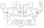
- FIGUREshows a diagram of a deposition chamber and a related process chemical delivery system according to an embodiment of the present invention.
- the inventionencompasses a deposition system.
- the deposition systemincludes a deposition chamber and a reservoir configured for containment of a metastable specie.
- the reservoirincludes an outlet port that is in selective fluid communication with an inlet port of the deposition chamber.
- the systemalso includes a metastable specie generating catalyst within the reservoir.
- the inventionencompasses an atomic layer deposition apparatus.
- the apparatusincludes a deposition chamber that contains a substrate platform and has a first inlet and a second inlet.
- the deposition chambercontains a dispersion head positioned between the first inlet and the substrate platform and between the second inlet and the substrate platform.
- the atomic layer deposition apparatusalso includes a first active specie containment reservoir in fluid communication with the deposition chamber through the first inlet, and a second active specie containment reservoir in fluid communication with the deposition chamber through the second inlet.
- One or more sources of carrier gasare configured to deliver carrier gas through at least one of the first inlet and the second inlet.
- the inventionencompasses an atomic layer deposition method.
- a metastable specieis contained within a metastable-specie-containment reservoir.
- the metastable-specie-containment reservoiris in selective fluid communication with a reaction chamber and the metastable specie is flowed from the metastable-specie-containment reservoir into the reaction chamber.
- the flowing of the metastable specie from the metastable-specie-containment reservoirincludes purging the metastable-specie-containment reservoir to flush the metastable specie from the reservoir into the reaction chamber through one or more metastable specie inlets.
- the flowing of the metastable specie from the metastable-specie-containment reservoiralso includes compressing the metastable specie into the reaction chamber which has a volume that is less than the initial volume occupied by the metastable specie prior to flowing the metastable specie from the containment reservoir.
- Atomic layer depositioninvolves formation of successive atomic layers on a substrate. Such layers may comprise an epitaxial, polycrystalline, amorphous, etc. material. ALD may also be referred to as atomic layer epitaxy, atomic layer processing, etc. Further, the invention may encompass other deposition methods not traditionally referred to as ALD, for example, chemical vapor deposition (CVD), but nevertheless including the method steps described herein. The deposition methods herein may be described in the context of formation on a semiconductor wafer. However, the invention encompasses deposition on a variety of substrates besides semiconductor substrates.
- ALDincludes exposing an initial substrate to a first chemical specie to accomplish chemisorption of the specie onto the substrate.
- the chemisorptionforms a monolayer that is uniformly one atom or molecule thick on the entire exposed initial substrate.
- a saturated monolayerPractically, as further described below, chemisorption might not occur on all portions of the substrate. Nevertheless, such an imperfect monolayer is still a monolayer in the context of this document. In many applications, merely a substantially saturated monolayer may be suitable.
- a substantially saturated monolayeris one that will still yield a deposited layer exhibiting the quality and/or properties desired for such layer.
- the first specieis purged from over the substrate and a second chemical specie is provided to chemisorb onto the first monolayer of the first specie.
- the second specieis then purged and the steps are repeated with exposure of the second specie monolayer to the first specie.
- the two monolayersmay be of the same specie.
- the second speciemight not add a monolayer, but rather chemisorb onto and remove some portion of the first monolayer.
- a third specie or moremay be successively chemisorbed and purged just as described for the first and second species.
- Purgingmay involve a variety of techniques including, but not limited to, contacting the substrate and/or monolayer with a carrier gas and/or lowering pressure to below the deposition pressure to reduce the concentration of a specie contacting the substrate and/or chemisorbed specie.
- carrier gasesinclude N 2 , Ar, He, etc.
- Purgingmay instead include contacting the substrate and/or monolayer with any substance that allows chemisorption byproducts to desorb and reduces the concentration of a contacting specie preparatory to introducing another specie.
- the contacting speciemay be reduced to some suitable concentration or partial pressure known to those skilled in the art based on the specifications for the product of a particular deposition process.
- ALDis often described as a self-limiting process, in that a finite number of sites exist on a substrate to which the first specie may form chemical bonds. The second specie might only bond to the first specie and thus may also be self-limiting. Once all of the finite number of sites on a substrate are bonded with a first specie, the first specie will often not bond to other of the first specie already bonded with the substrate.
- process conditionscan be varied in ALD to promote such bonding and render ALD not self-limiting. Accordingly, ALD may also encompass a specie forming other than one monolayer at a time by stacking of a specie, forming a layer more than one atom or molecule thick.
- ALDatomic layer deposition
- ALDatomic layer deposition
- CVDchemical vapor deposition
- plasma enhanced CVDplasma enhanced CVD
- CVDis commonly used to form non-selectively a complete, deposited material on a substrate.
- One characteristic of CVDis the simultaneous presence of multiple species in the deposition chamber that react to form the deposited material. Such condition is contrasted with the purging criteria for traditional ALD wherein a substrate is contacted with a single deposition specie that chemisorbs to a substrate or previously deposited specie.
- An ALD process regimemay provide a simultaneously contacted plurality of species of a type or under conditions such that ALD chemisorption, rather than CVD reaction occurs.
- the speciesmay chemisorb to a substrate or previously deposited specie, providing a surface onto which subsequent specie may next chemisorb to form a complete layer of desired material.
- depositionoccurs largely independent of the composition or surface properties of an underlying substrate.
- chemisorption rate in ALDmight be influenced by the composition, crystalline structure, and other properties of a substrate or chemisorbed specie.
- Other process conditionsfor example, pressure and temperature, may also influence chemisorption rate.
- Deposition system 10includes a deposition chamber 12 having one or more inlet ports 16 , 34 and a substrate platform 24 configured for retaining a substrate 26 .
- a disperser 28can be positioned within deposition chamber 12 , between substrate platform 24 and the inlet ports. Numerous forms of disperser 28 can be utilized for purposes of the present invention including, but not limited to, a porous dispersion head or shower head.
- the deposition systemalso includes one or more reservoirs 14 , 30 in selective fluid communication with the inlet ports of deposition chamber 12 .
- reservoirs 14 , 30in selective fluid communication with the inlet ports of deposition chamber 12 .
- selective fluid communicationrefers to fluid communication which can be selectively halted to result in fluid isolation of a reservoir or other compartment from the deposition chamber.
- Selective fluid communication from reservoirs 14 and 30can comprise communication from reservoir outlet ports 18 and 32 respectively and through inlet ports 16 and 34 of deposition chamber 12 .
- Selective fluid communication between reservoirs 14 and 30 , and deposition chamber 12can be achieved by providing independent deposition chamber inlet ports 16 and 34 in selective fluid communication with respective reservoir outlet ports 18 and 32 , as shown in the FIGURE, or alternatively can be through a common inlet port (not shown) which provides selective fluid communication from both reservoir 14 and reservoir 30 into deposition chamber 12 .
- the one or more reservoirs of the present inventioncan be two reservoirs 14 and 30 , as depicted in the FIGURE.
- deposition system 10can comprise a single reservoir (not shown), or more than two reservoirs (not shown).
- deposition system 10can be configured such that the one or more reservoirs and deposition chamber 12 are within a common unit.
- at least one reservoir wall 52can be coextensive with a wall 50 of deposition chamber 12 .
- the one or more reservoirscan be independent relative to the each other, relative to deposition chamber 12 , or both.
- One or more metastable or activated precursor materialscan be provided within reservoirs 14 and 30 .
- metastablecan refer to any metastable form of a precursor material, including but not limited to an activated form. It can be advantageous to provide the reservoirs of the present invention proximate deposition chamber 12 to limit the flowpath for fluid communication between the reservoirs and deposition chamber 12 and thereby minimize any decay in a metastable specie that may occur while flowing a metastable precursor material from a reservoir into the deposition chamber.
- Reservoirs 14 and 30can be configured for containment of the one or more metastable precursors.
- the one or more reservoirscan alternatively be referred to as reservoirs, as containment reservoirs, or as metastable-specie-containment reservoirs.
- Containment of the metastable precursors within the reservoirscan comprise halting selective fluid communication from the reservoirs, and can comprise, for instance, closing a valve 48 that can be positioned between reservoir outlets 18 , 32 and the corresponding deposition chamber inlet 16 , 34 .
- a valve 48shows a valve, it is to be understood that numerous alternative isolation methods can be utilized.
- the providing a metastable specie of a precursor within a single reservoir 14 , 30can comprise one or both of generation of the metastable specie within the reservoir and remote generation of the metastable specie.
- Generation of a metastable specie within a reservoircan comprise providing a source of precursor material 42 , flowing the precursor material into reservoir 14 through a reservoir inlet 19 , and treating the precursor material within the reservoir to generate a metastable form of the precursor material.
- FIGUREshows a single source of precursor material 42 providing precursor material to reservoir 14 , is to be understood that a plurality of precursor sources can be provided (not shown).
- two or more different precursor materialscan be provided to a reservoir and can be allowed to premix within the reservoir and, in particular embodiments can be activated or can be partially reacted together to form a desired metastable species.
- TiCl 4 and B 2 H 6can be premixed and activated to form a metastable species within a common reservoir 14 .
- Treating of a precursor material to generate a metastable specie within reservoir 14is not limited to a particular treatment and can include treatment comprising one or more of a catalyst, heat, plasma, UV light, microwave, electromagnetic radiation, electron-gun or sound.
- a metastable speciecan be catalytically generated within a reservoir 14 by providing a metastable specie generating catalyst 20 within the reservoir.
- deposition system 10can include a heat source (not shown) which can be configured to heat catalyst 20 .
- Catalyst 20is not limited to any specific catalyst and can comprise one or more of platinum, platinum alloys, zinc, nickel, and palladium.
- reservoir 14can comprise one or more of a heat source and a plasma source within the reservoir for generation of a metastable specie.
- deposition apparatus 10can include one or more remote metastable specie generating sources 38 in fluid communication with one or more of the reservoirs.
- FIGUREdepicts a single remote metastable specie generating source 38 in fluid communication with a single reservoir 30 , it is to be understood that the invention encompasses embodiments having multiple remote metastable specie generating sources (not shown) in fluid communication with one or more containment reservoirs.
- Remote metastable 38 generating sourcecan comprise any of the metastable specie generating methods discussed above with respect to generation within reservoir 14 .
- deposition system 10can comprise a single precursor source 44 configured to provide precursor material into remote metastable specie generating source 38 through a reservoir inlet 40 .
- multiple precursor material sourcescan be configured to provide a single or multiple precursors into remote metastable specie generating source 38 (not shown).
- the volume of containment reservoirs 14 and 30is not limited to a specific value and can, for example, be greater than about 5.0 ml. Described relative to an internal volume of deposition chamber 12 , a containment reservoir 14 , 30 can comprise an individual volume of from about 1% of the internal volume of deposition chamber 12 to about 3 times the internal volume of deposition chamber 12 . In particular embodiments, the combined value of the reservoirs comprised by the system of the present invention can be, for example, equal to or greater than the volume within deposition chamber 12 . It is advantageous to provide relatively large volume reservoirs 14 and 30 to alleviate the detrimental effect of high pressure upon the lifetime of metastable species, and to minimize the occurrence of unwanted side reactions between molecules of a metastable specie.
- Deposition system 10can comprise one or more carrier gas sources 22 and 36 configured to deliver carrier gas through at least one reaction chamber inlet port 16 and 34 .
- carrier gases 22 and 36are provided into reaction chamber 12 through inlet port 16 and 34 without passing through reservoirs 14 and 30 .
- the present inventionencompasses embodiments where one or more carrier gas 22 or 36 is provided to flow through one or more of reservoir 14 and 30 prior to flowing into reaction chamber 12 through the respective inlet port 16 and 34 .
- Numerous gasesare available for utilization as a carrier gas for purposes of the present invention. The particular gas can be selected based upon the precursor material to be utilized.
- the carrier gas selectedis preferably inert with respect to the particular precursor material, and with respect to the metastable forms thereof that are generated by the methods of the present invention.
- Such gascan comprise, but is not limited too, one or more of N 2 , Ar, He H 2 , Ne and Kr.
- metastable specie of precursor materialcan be either flowed directly into deposition chamber 12 , or contained within the respective reservoir and selectively flowed from the reservoir into deposition chamber 12 through inlet port 16 , 34 .
- deposition system 10can comprise two reservoirs, a first metastable specie can be generated within a first reservoir 14 and a second metastable specie can be generated within a second reservoir 30 .
- Generation of second metastable speciecan utilize any of the generation methods discussed above with respect to generation within reservoir 14 .
- generation of the second metastable speciecan include providing a catalyst 31 within reservoir 30 .
- Catalyst 31is not limited to any specific material and can comprise, for example, any of the materials discussed above with respect to catalyst 20 .
- Catalyst 31can comprise the same material as catalyst 20 or can comprise a material different from the material of catalyst 20 .
- the second metastable speciecan be remotely formed and provided to second reservoir 30 in metastable form.
- the inventionencompasses embodiments having a single reservoir, and that generation of a metastable specie can occur within the single reservoir or can occur at a location remote from the single reservoir and the precursor material provided into the reservoir in a metastable form.
- the particular aspects of the inventioncan utilize a deposition system 10 comprising more than two reservoirs and can be configured for generation of metastable species within at least two of the two or more reservoirs.
- the inventionalso contemplates embodiments having two of more reservoirs where at least two reservoirs are configured for receipt of remotely generated metastable precursor. It is to be understood that, in embodiments comprising two or more reservoirs, any number or all of such reservoirs can contain the same precursor material, each reservoir may contain different a precursor material, or any combination thereof.
- a layer 46can be formed on a substrate 26 provided on a substrate platform 24 within deposition chamber 12 .
- One or more metastable speciescan be selectively flowed from one or more of reservoir 14 and 30 into deposition chamber 12 through one or more inlet ports 16 and 34 .
- Deposition of layer 46can comprise flowing a first metastable specie from a first reservoir 14 through chamber inlet port 16 , passing the metastable specie through disperser 28 and depositing at least some of the metastable precursor onto substrate 26 .
- Formation of layer 46can further include flowing a second metastable specie from a second reservoir 30 through inlet port 34 , passing the second metastable specie through disperser 28 , and depositing at least some of the second metastable specie onto substrate 26 .
- the first and the second precursorcan be flowed simultaneously relative to one another, can be flowed sequentially, or the flowing of the second precursor can partially overlap the flowing of the first precursor.
- Deposition methods encompassed by the present inventioncan include embodiments appropriate for ALD applications, where the first metastable specie and the second metastable specie are flowed into the deposition chamber sequentially relative to one another.
- deposition chamber 12can be purged after flowing the first metastable specie and prior to flowing of the second metastable specie by, for example, flowing a purge gas through the deposition chamber (not shown).
- the present inventioncan be utilized during, for example, CVD applications where a first precursor and a second precursor are allowed to mix prior to or during layer formation.
- the inventioncan also be utilized for pulsed CVD applications where at least some of a first precursor is deposited onto the substrate prior to introduction of a second precursor.
- deposition system 10can also include additional precursor sources configured to provide one or more additional activated or non-activated precursor material directly into deposition chamber 12 without passing though reservoirs 14 and 30 (not shown).
- additional precursor materialcan be utilized during, for example, ALD, CVD or pulsed CVD applications, in conjunction with one or more metastable species provided from one or more of reservoirs 14 and 30 .
- precursor materialscan be utilized for purposes of the present invention including but not limited to H 2 , TiCl 4 , O 2 , NO, TaF 5 , NH3, trimethyl aluminum (TMA), SiH 4 , O 3 , and tetrakis(dimethylamino) titanium (TDMAT). Accordingly, numerous metastable species of precursor materials can be generated.
- a source of precursor material 42 comprising hydrogen gasis provided, the hydrogen gas comprising material is flowed from precursor source 42 into reservoir 14 .
- Activated hydrogencan be generated within chamber 14 by, for example, providing a catalyst 20 which can comprise, for instance, platinum.
- the activated hydrogen speciecan be contained within reservoir 14 prior to flowing the activated hydrogen into deposition chamber 12 . It can be advantageous to contain the activated hydrogen precursor within reservoir 14 prior to flowing the activated precursor into deposition chamber 12 to increase the time of the exposure of the precursor hydrogen to the catalyst or other metastable specie generating source, and thereby enhance or maximize formation of the metastable specie prior to deposition.
- the activated hydrogencan be selectively flowed from reservoir 14 into deposition chamber 12 , and such flowing can be assisted by flowing carrier gas 22 through inlet 16 .
- Flowing of activated hydrogencan comprise flowing from reservoir 14 having a reservoir volume of greater than or equal to about 1% of the internal volume comprised by deposition chamber 12 .
- reservoir 14can comprise a volume greater than the internal volume the deposition chamber and the flowing of activated hydrogen from the reservoir into the deposition chamber can include compression of the activated hydrogen. It can be advantageous for reservoir 14 to comprise a relatively large volume to prolong the lifetime of the activated hydrogen specie prior to flowing the activated hydrogen into the deposition chamber.
- deposition chamber 12can be purged after flowing the activated hydrogen and prior to any subsequent flowing of precursor material.
- a second precursor materialfor example TiCl 4
- a second precursor materialcan be flowed into deposition chamber 12 and at least some of the second precursor can be adsorbed onto substrate 26 to react with the previously adsoprbed activated hydrogen to form layer 46 .
- deposition chamber 12can be purged, for example, by flowing a purge gas through the deposition chamber (not shown). Repeated rounds of sequentially flowing activated hydrogen and TiCl 4 can be performed according to the present invention to achieve a desired thickness of layer 46 .
Landscapes
- Chemical & Material Sciences (AREA)
- Engineering & Computer Science (AREA)
- Chemical Kinetics & Catalysis (AREA)
- General Chemical & Material Sciences (AREA)
- Materials Engineering (AREA)
- Mechanical Engineering (AREA)
- Metallurgy (AREA)
- Organic Chemistry (AREA)
- Physics & Mathematics (AREA)
- Condensed Matter Physics & Semiconductors (AREA)
- General Physics & Mathematics (AREA)
- Manufacturing & Machinery (AREA)
- Computer Hardware Design (AREA)
- Microelectronics & Electronic Packaging (AREA)
- Power Engineering (AREA)
- Chemical Vapour Deposition (AREA)
Abstract
Description
- The present invention pertains to deposition apparatuses and methods for forming layers over a semiconductor substrate.[0001]
- Layer deposition techniques such as the various forms of chemical vapor deposition (CVD), pulsed CVD, and atomic layer deposition (ALD), are utilized to form layers upon surfaces, including surfaces of semiconductor substrates. These techniques involve providing precursor materials which react chemically to form a layer upon the surface.[0002]
- Due to low reactivities of some precursor materials utilized in the deposition techniques described above, it is often desirable to enhance reactivity of precursors by generation of a metastable or an activated form of the precursor material. Once generated, the lifetimes of the metastable or activated species of the precursors are pressure dependent. Specifically, the lifetimes of metastable or activated species shorten as a result of increased pressure. Additionally, the number of unwanted side reactions between activated or metastable specie molecules increases with increased pressure. Generally, conventional layer deposition techniques that utilize metastable or activated precursors, generate or contain such precursors within a small volume under high pressure and thereby detrimentally affect the longevity of the metastable or activated form and promote unwanted side reactions.[0003]
- Accordingly, it would be desirable to provide alternative methods and apparatuses for layer deposition.[0004]
- Preferred embodiments of the invention are described below with reference to the following accompanying drawing.[0005]
- The FIGURE shows a diagram of a deposition chamber and a related process chemical delivery system according to an embodiment of the present invention.[0006]
- In one aspect the invention encompasses a deposition system. The deposition system includes a deposition chamber and a reservoir configured for containment of a metastable specie. The reservoir includes an outlet port that is in selective fluid communication with an inlet port of the deposition chamber. The system also includes a metastable specie generating catalyst within the reservoir.[0007]
- In one aspect, the invention encompasses an atomic layer deposition apparatus. The apparatus includes a deposition chamber that contains a substrate platform and has a first inlet and a second inlet. The deposition chamber contains a dispersion head positioned between the first inlet and the substrate platform and between the second inlet and the substrate platform. The atomic layer deposition apparatus also includes a first active specie containment reservoir in fluid communication with the deposition chamber through the first inlet, and a second active specie containment reservoir in fluid communication with the deposition chamber through the second inlet. One or more sources of carrier gas are configured to deliver carrier gas through at least one of the first inlet and the second inlet.[0008]
- In one aspect the invention encompasses an atomic layer deposition method. A metastable specie is contained within a metastable-specie-containment reservoir. The metastable-specie-containment reservoir is in selective fluid communication with a reaction chamber and the metastable specie is flowed from the metastable-specie-containment reservoir into the reaction chamber. The flowing of the metastable specie from the metastable-specie-containment reservoir includes purging the metastable-specie-containment reservoir to flush the metastable specie from the reservoir into the reaction chamber through one or more metastable specie inlets. The flowing of the metastable specie from the metastable-specie-containment reservoir also includes compressing the metastable specie into the reaction chamber which has a volume that is less than the initial volume occupied by the metastable specie prior to flowing the metastable specie from the containment reservoir.[0009]
- This disclosure of the invention is submitted in furtherance of the constitutional purposes of the U.S. Patent Laws “to promote the progress of science and useful arts” (Article 1, Section 8).[0010]
- Atomic layer deposition (ALD) involves formation of successive atomic layers on a substrate. Such layers may comprise an epitaxial, polycrystalline, amorphous, etc. material. ALD may also be referred to as atomic layer epitaxy, atomic layer processing, etc. Further, the invention may encompass other deposition methods not traditionally referred to as ALD, for example, chemical vapor deposition (CVD), but nevertheless including the method steps described herein. The deposition methods herein may be described in the context of formation on a semiconductor wafer. However, the invention encompasses deposition on a variety of substrates besides semiconductor substrates.[0011]
- Described in summary, ALD includes exposing an initial substrate to a first chemical specie to accomplish chemisorption of the specie onto the substrate. Theoretically, the chemisorption forms a monolayer that is uniformly one atom or molecule thick on the entire exposed initial substrate. In other words, a saturated monolayer. Practically, as further described below, chemisorption might not occur on all portions of the substrate. Nevertheless, such an imperfect monolayer is still a monolayer in the context of this document. In many applications, merely a substantially saturated monolayer may be suitable. A substantially saturated monolayer is one that will still yield a deposited layer exhibiting the quality and/or properties desired for such layer.[0012]
- The first specie is purged from over the substrate and a second chemical specie is provided to chemisorb onto the first monolayer of the first specie. The second specie is then purged and the steps are repeated with exposure of the second specie monolayer to the first specie. In some cases, the two monolayers may be of the same specie. Also, the second specie might not add a monolayer, but rather chemisorb onto and remove some portion of the first monolayer. Further, a third specie or more may be successively chemisorbed and purged just as described for the first and second species.[0013]
- Purging may involve a variety of techniques including, but not limited to, contacting the substrate and/or monolayer with a carrier gas and/or lowering pressure to below the deposition pressure to reduce the concentration of a specie contacting the substrate and/or chemisorbed specie. Examples of carrier gases include N[0014]2, Ar, He, etc. Purging may instead include contacting the substrate and/or monolayer with any substance that allows chemisorption byproducts to desorb and reduces the concentration of a contacting specie preparatory to introducing another specie. The contacting specie may be reduced to some suitable concentration or partial pressure known to those skilled in the art based on the specifications for the product of a particular deposition process.
- ALD is often described as a self-limiting process, in that a finite number of sites exist on a substrate to which the first specie may form chemical bonds. The second specie might only bond to the first specie and thus may also be self-limiting. Once all of the finite number of sites on a substrate are bonded with a first specie, the first specie will often not bond to other of the first specie already bonded with the substrate. However, process conditions can be varied in ALD to promote such bonding and render ALD not self-limiting. Accordingly, ALD may also encompass a specie forming other than one monolayer at a time by stacking of a specie, forming a layer more than one atom or molecule thick. The various aspects of the present invention described herein are applicable to any circumstance where ALD may be desired. A few examples of materials that may be deposited by ALD include platinum, rhodium, iridium, ruthenium, osmium, palladium, or mixtures thereof, titanium nitride, and others.[0015]
- Often, traditional ALD occurs within an often-used range of temperature and pressure and according to established purging criteria to achieve the desired formation of an overall ALD layer one monolayer at a time. Even so, ALD conditions can vary greatly depending on the particular precursors, layer composition, deposition equipment, and other factors according to criteria known by those skilled in the art. Maintaining the traditional conditions of temperature, pressure, and purging minimizes unwanted reactions that may impact monolayer formation and quality of the resulting overall ALD layer. Accordingly, operating outside the traditional temperature and pressure ranges may risk formation of defective monolayers.[0016]
- The general technology of chemical vapor deposition (CVD) includes a variety of more specific processes, including, but not limited to, plasma enhanced CVD and others. CVD is commonly used to form non-selectively a complete, deposited material on a substrate. One characteristic of CVD is the simultaneous presence of multiple species in the deposition chamber that react to form the deposited material. Such condition is contrasted with the purging criteria for traditional ALD wherein a substrate is contacted with a single deposition specie that chemisorbs to a substrate or previously deposited specie. An ALD process regime may provide a simultaneously contacted plurality of species of a type or under conditions such that ALD chemisorption, rather than CVD reaction occurs. Instead of reacting together, the species may chemisorb to a substrate or previously deposited specie, providing a surface onto which subsequent specie may next chemisorb to form a complete layer of desired material. Under most CVD conditions, deposition occurs largely independent of the composition or surface properties of an underlying substrate. By contrast, chemisorption rate in ALD might be influenced by the composition, crystalline structure, and other properties of a substrate or chemisorbed specie. Other process conditions, for example, pressure and temperature, may also influence chemisorption rate.[0017]
- The present invention is described with reference to the FIGURE which shows a[0018]
deposition system 10 encompassed by an aspect of the present invention.Deposition system 10 includes adeposition chamber 12 having one ormore inlet ports substrate platform 24 configured for retaining asubstrate 26. Adisperser 28 can be positioned withindeposition chamber 12, betweensubstrate platform 24 and the inlet ports. Numerous forms ofdisperser 28 can be utilized for purposes of the present invention including, but not limited to, a porous dispersion head or shower head. - The deposition system also includes one or[0019]
more reservoirs deposition chamber 12. For purposes of the present description, use of the term “selective fluid communication” refers to fluid communication which can be selectively halted to result in fluid isolation of a reservoir or other compartment from the deposition chamber. Selective fluid communication fromreservoirs reservoir outlet ports inlet ports deposition chamber 12. Selective fluid communication betweenreservoirs deposition chamber 12 can be achieved by providing independent depositionchamber inlet ports reservoir outlet ports reservoir 14 andreservoir 30 intodeposition chamber 12. - The one or more reservoirs of the present invention can be two[0020]
reservoirs deposition system 10 can comprise a single reservoir (not shown), or more than two reservoirs (not shown). As shown in the FIGURE,deposition system 10 can be configured such that the one or more reservoirs anddeposition chamber 12 are within a common unit. In embodiments having one or more reservoir anddeposition chamber 12 within a common unit, at least onereservoir wall 52 can be coextensive with awall 50 ofdeposition chamber 12. Alternatively, the one or more reservoirs can be independent relative to the each other, relative todeposition chamber 12, or both. - One or more metastable or activated precursor materials can be provided within[0021]
reservoirs proximate deposition chamber 12 to limit the flowpath for fluid communication between the reservoirs anddeposition chamber 12 and thereby minimize any decay in a metastable specie that may occur while flowing a metastable precursor material from a reservoir into the deposition chamber. - [0022]
Reservoirs valve 48 that can be positioned betweenreservoir outlets deposition chamber inlet - In particular aspects of the present invention, the providing a metastable specie of a precursor within a[0023]
single reservoir precursor material 42, flowing the precursor material intoreservoir 14 through areservoir inlet 19, and treating the precursor material within the reservoir to generate a metastable form of the precursor material. Although the FIGURE shows a single source ofprecursor material 42 providing precursor material toreservoir 14, is to be understood that a plurality of precursor sources can be provided (not shown). In addition, two or more different precursor materials can be provided to a reservoir and can be allowed to premix within the reservoir and, in particular embodiments can be activated or can be partially reacted together to form a desired metastable species. For instance, TiCl4and B2H6can be premixed and activated to form a metastable species within acommon reservoir 14. - Treating of a precursor material to generate a metastable specie within[0024]
reservoir 14 is not limited to a particular treatment and can include treatment comprising one or more of a catalyst, heat, plasma, UV light, microwave, electromagnetic radiation, electron-gun or sound. - As shown in FIG. 1, a metastable specie can be catalytically generated within a[0025]
reservoir 14 by providing a metastablespecie generating catalyst 20 within the reservoir. Additionally,deposition system 10 can include a heat source (not shown) which can be configured to heatcatalyst 20.Catalyst 20 is not limited to any specific catalyst and can comprise one or more of platinum, platinum alloys, zinc, nickel, and palladium. In addition to or in place ofcatalyst 20,reservoir 14 can comprise one or more of a heat source and a plasma source within the reservoir for generation of a metastable specie. - In aspects of the present invention where one or more metastable species are remotely generated,[0026]
deposition apparatus 10 can include one or more remote metastablespecie generating sources 38 in fluid communication with one or more of the reservoirs. Although the FIGURE depicts a single remote metastablespecie generating source 38 in fluid communication with asingle reservoir 30, it is to be understood that the invention encompasses embodiments having multiple remote metastable specie generating sources (not shown) in fluid communication with one or more containment reservoirs. Remote metastable38 generating source can comprise any of the metastable specie generating methods discussed above with respect to generation withinreservoir 14. As shown in the FIGURE,deposition system 10 can comprise asingle precursor source 44 configured to provide precursor material into remote metastablespecie generating source 38 through areservoir inlet 40. Alternatively, multiple precursor material sources can be configured to provide a single or multiple precursors into remote metastable specie generating source38 (not shown). - The volume of[0027]
containment reservoirs deposition chamber 12, acontainment reservoir deposition chamber 12 to about 3 times the internal volume ofdeposition chamber 12. In particular embodiments, the combined value of the reservoirs comprised by the system of the present invention can be, for example, equal to or greater than the volume withindeposition chamber 12. It is advantageous to provide relativelylarge volume reservoirs - [0028]
Deposition system 10 can comprise one or morecarrier gas sources chamber inlet port carrier gases reaction chamber 12 throughinlet port reservoirs more carrier gas reservoir reaction chamber 12 through therespective inlet port - Once a metastable specie of precursor material is provided within one or more of[0029]
reservoirs deposition chamber 12, or contained within the respective reservoir and selectively flowed from the reservoir intodeposition chamber 12 throughinlet port - As depicted in the FIGURE,[0030]
deposition system 10 can comprise two reservoirs, a first metastable specie can be generated within afirst reservoir 14 and a second metastable specie can be generated within asecond reservoir 30. Generation of second metastable specie can utilize any of the generation methods discussed above with respect to generation withinreservoir 14. As shown in the FIGURE, generation of the second metastable specie can include providing acatalyst 31 withinreservoir 30.Catalyst 31 is not limited to any specific material and can comprise, for example, any of the materials discussed above with respect tocatalyst 20.Catalyst 31 can comprise the same material ascatalyst 20 or can comprise a material different from the material ofcatalyst 20. Alternatively, the second metastable specie can be remotely formed and provided tosecond reservoir 30 in metastable form. - It is to be understood that the invention encompasses embodiments having a single reservoir, and that generation of a metastable specie can occur within the single reservoir or can occur at a location remote from the single reservoir and the precursor material provided into the reservoir in a metastable form.[0031]
- In addition to the features described above, the particular aspects of the invention can utilize a[0032]
deposition system 10 comprising more than two reservoirs and can be configured for generation of metastable species within at least two of the two or more reservoirs. The invention also contemplates embodiments having two of more reservoirs where at least two reservoirs are configured for receipt of remotely generated metastable precursor. It is to be understood that, in embodiments comprising two or more reservoirs, any number or all of such reservoirs can contain the same precursor material, each reservoir may contain different a precursor material, or any combination thereof. It can be advantageous in certain deposition applications, to provide a plurality of reservoirs for generation, containment, or both generation and containment of a single metastable precursor material to allow an enhanced build-up of the activated form to occur prior to flowing the precursor intodeposition chamber 12. - In methods encompassed by the present invention, a[0033]
layer 46 can be formed on asubstrate 26 provided on asubstrate platform 24 withindeposition chamber 12. One or more metastable species can be selectively flowed from one or more ofreservoir deposition chamber 12 through one ormore inlet ports layer 46 can comprise flowing a first metastable specie from afirst reservoir 14 throughchamber inlet port 16, passing the metastable specie throughdisperser 28 and depositing at least some of the metastable precursor ontosubstrate 26. Formation oflayer 46 can further include flowing a second metastable specie from asecond reservoir 30 throughinlet port 34, passing the second metastable specie throughdisperser 28, and depositing at least some of the second metastable specie ontosubstrate 26. - In aspects of the present invention utilizing a first and a second metastable precursor, the first and the second precursor can be flowed simultaneously relative to one another, can be flowed sequentially, or the flowing of the second precursor can partially overlap the flowing of the first precursor. Deposition methods encompassed by the present invention can include embodiments appropriate for ALD applications, where the first metastable specie and the second metastable specie are flowed into the deposition chamber sequentially relative to one another. Furthermore,[0034]
deposition chamber 12 can be purged after flowing the first metastable specie and prior to flowing of the second metastable specie by, for example, flowing a purge gas through the deposition chamber (not shown). - The present invention can be utilized during, for example, CVD applications where a first precursor and a second precursor are allowed to mix prior to or during layer formation. The invention can also be utilized for pulsed CVD applications where at least some of a first precursor is deposited onto the substrate prior to introduction of a second precursor.[0035]
- In addition to the features described above,[0036]
deposition system 10 can also include additional precursor sources configured to provide one or more additional activated or non-activated precursor material directly intodeposition chamber 12 without passing thoughreservoirs 14 and30 (not shown). Such additional precursor material can be utilized during, for example, ALD, CVD or pulsed CVD applications, in conjunction with one or more metastable species provided from one or more ofreservoirs - Numerous precursor materials can be utilized for purposes of the present invention including but not limited to H[0037]2, TiCl4, O2, NO, TaF5, NH3, trimethyl aluminum (TMA), SiH4, O3, and tetrakis(dimethylamino) titanium (TDMAT). Accordingly, numerous metastable species of precursor materials can be generated.
- In one specific aspect of the present invention, a source of[0038]
precursor material 42 comprising hydrogen gas is provided, the hydrogen gas comprising material is flowed fromprecursor source 42 intoreservoir 14. Activated hydrogen can be generated withinchamber 14 by, for example, providing acatalyst 20 which can comprise, for instance, platinum. The activated hydrogen specie can be contained withinreservoir 14 prior to flowing the activated hydrogen intodeposition chamber 12. It can be advantageous to contain the activated hydrogen precursor withinreservoir 14 prior to flowing the activated precursor intodeposition chamber 12 to increase the time of the exposure of the precursor hydrogen to the catalyst or other metastable specie generating source, and thereby enhance or maximize formation of the metastable specie prior to deposition. - The activated hydrogen can be selectively flowed from[0039]
reservoir 14 intodeposition chamber 12, and such flowing can be assisted by flowingcarrier gas 22 throughinlet 16. Flowing of activated hydrogen can comprise flowing fromreservoir 14 having a reservoir volume of greater than or equal to about 1% of the internal volume comprised bydeposition chamber 12. In particular embodiments,reservoir 14 can comprise a volume greater than the internal volume the deposition chamber and the flowing of activated hydrogen from the reservoir into the deposition chamber can include compression of the activated hydrogen. It can be advantageous forreservoir 14 to comprise a relatively large volume to prolong the lifetime of the activated hydrogen specie prior to flowing the activated hydrogen into the deposition chamber. - When[0040]
deposition system 10 comprises an atomic layer deposition system,deposition chamber 12 can be purged after flowing the activated hydrogen and prior to any subsequent flowing of precursor material. After adsorption of at least some of the activated hydrogen ontosubstrate 26, a second precursor material, for example TiCl4, can be flowed intodeposition chamber 12 and at least some of the second precursor can be adsorbed ontosubstrate 26 to react with the previously adsoprbed activated hydrogen to formlayer 46. - After flowing the TiCl[0041]4,
deposition chamber 12 can be purged, for example, by flowing a purge gas through the deposition chamber (not shown). Repeated rounds of sequentially flowing activated hydrogen and TiCl4can be performed according to the present invention to achieve a desired thickness oflayer 46. - In compliance with the statute, the invention has been described in language more or less specific as to structural and methodical features. It is to be understood, however, that the invention is not limited to the specific features shown and described, since the means herein disclosed comprise preferred forms of putting the invention into effect. The invention is, therefore, claimed in any of its forms or modifications within the proper scope of the appended claims appropriately interpreted in accordance with the doctrine of equivalents.[0042]
Claims (48)
Priority Applications (1)
| Application Number | Priority Date | Filing Date | Title |
|---|---|---|---|
| US10/715,628US7527693B2 (en) | 2002-02-25 | 2003-11-17 | Apparatus for improved delivery of metastable species |
Applications Claiming Priority (2)
| Application Number | Priority Date | Filing Date | Title |
|---|---|---|---|
| US10/085,588US6787185B2 (en) | 2002-02-25 | 2002-02-25 | Deposition methods for improved delivery of metastable species |
| US10/715,628US7527693B2 (en) | 2002-02-25 | 2003-11-17 | Apparatus for improved delivery of metastable species |
Related Parent Applications (1)
| Application Number | Title | Priority Date | Filing Date |
|---|---|---|---|
| US10/085,588DivisionUS6787185B2 (en) | 2002-02-25 | 2002-02-25 | Deposition methods for improved delivery of metastable species |
Publications (2)
| Publication Number | Publication Date |
|---|---|
| US20040094092A1true US20040094092A1 (en) | 2004-05-20 |
| US7527693B2 US7527693B2 (en) | 2009-05-05 |
Family
ID=22192630
Family Applications (3)
| Application Number | Title | Priority Date | Filing Date |
|---|---|---|---|
| US10/085,588Expired - LifetimeUS6787185B2 (en) | 2002-02-25 | 2002-02-25 | Deposition methods for improved delivery of metastable species |
| US10/715,628Expired - LifetimeUS7527693B2 (en) | 2002-02-25 | 2003-11-17 | Apparatus for improved delivery of metastable species |
| US10/852,784Expired - LifetimeUS7393562B2 (en) | 2002-02-25 | 2004-05-24 | Deposition methods for improved delivery of metastable species |
Family Applications Before (1)
| Application Number | Title | Priority Date | Filing Date |
|---|---|---|---|
| US10/085,588Expired - LifetimeUS6787185B2 (en) | 2002-02-25 | 2002-02-25 | Deposition methods for improved delivery of metastable species |
Family Applications After (1)
| Application Number | Title | Priority Date | Filing Date |
|---|---|---|---|
| US10/852,784Expired - LifetimeUS7393562B2 (en) | 2002-02-25 | 2004-05-24 | Deposition methods for improved delivery of metastable species |
Country Status (1)
| Country | Link |
|---|---|
| US (3) | US6787185B2 (en) |
Cited By (4)
| Publication number | Priority date | Publication date | Assignee | Title |
|---|---|---|---|---|
| US20120073499A1 (en)* | 2010-09-29 | 2012-03-29 | Hon Hai Precision Industry Co., Ltd. | Coating device |
| US20130203267A1 (en)* | 2012-02-06 | 2013-08-08 | Asm Ip Holding B.V. | Multiple vapor sources for vapor deposition |
| US11788190B2 (en) | 2019-07-05 | 2023-10-17 | Asm Ip Holding B.V. | Liquid vaporizer |
| US11946136B2 (en) | 2019-09-20 | 2024-04-02 | Asm Ip Holding B.V. | Semiconductor processing device |
Families Citing this family (459)
| Publication number | Priority date | Publication date | Assignee | Title |
|---|---|---|---|---|
| WO2002068508A1 (en)* | 2001-02-23 | 2002-09-06 | The Gates Corporation | Process for directly bonding rubber to at least a second substrate, and the resulting article |
| US6852167B2 (en) | 2001-03-01 | 2005-02-08 | Micron Technology, Inc. | Methods, systems, and apparatus for uniform chemical-vapor depositions |
| US6953730B2 (en) | 2001-12-20 | 2005-10-11 | Micron Technology, Inc. | Low-temperature grown high quality ultra-thin CoTiO3 gate dielectrics |
| US6787185B2 (en)* | 2002-02-25 | 2004-09-07 | Micron Technology, Inc. | Deposition methods for improved delivery of metastable species |
| US7439191B2 (en)* | 2002-04-05 | 2008-10-21 | Applied Materials, Inc. | Deposition of silicon layers for active matrix liquid crystal display (AMLCD) applications |
| US7374617B2 (en)* | 2002-04-25 | 2008-05-20 | Micron Technology, Inc. | Atomic layer deposition methods and chemical vapor deposition methods |
| US6861094B2 (en)* | 2002-04-25 | 2005-03-01 | Micron Technology, Inc. | Methods for forming thin layers of materials on micro-device workpieces |
| US7160577B2 (en) | 2002-05-02 | 2007-01-09 | Micron Technology, Inc. | Methods for atomic-layer deposition of aluminum oxides in integrated circuits |
| US7589029B2 (en) | 2002-05-02 | 2009-09-15 | Micron Technology, Inc. | Atomic layer deposition and conversion |
| US7045430B2 (en) | 2002-05-02 | 2006-05-16 | Micron Technology Inc. | Atomic layer-deposited LaAlO3 films for gate dielectrics |
| US6838114B2 (en)* | 2002-05-24 | 2005-01-04 | Micron Technology, Inc. | Methods for controlling gas pulsing in processes for depositing materials onto micro-device workpieces |
| US6896730B2 (en)* | 2002-06-05 | 2005-05-24 | Micron Technology, Inc. | Atomic layer deposition apparatus and methods |
| US7135421B2 (en) | 2002-06-05 | 2006-11-14 | Micron Technology, Inc. | Atomic layer-deposited hafnium aluminum oxide |
| KR100455297B1 (en)* | 2002-06-19 | 2004-11-06 | 삼성전자주식회사 | Manufacturing method of inorganic nano tube |
| US7118783B2 (en)* | 2002-06-26 | 2006-10-10 | Micron Technology, Inc. | Methods and apparatus for vapor processing of micro-device workpieces |
| US7221586B2 (en) | 2002-07-08 | 2007-05-22 | Micron Technology, Inc. | Memory utilizing oxide nanolaminates |
| US6821347B2 (en) | 2002-07-08 | 2004-11-23 | Micron Technology, Inc. | Apparatus and method for depositing materials onto microelectronic workpieces |
| US6921702B2 (en) | 2002-07-30 | 2005-07-26 | Micron Technology Inc. | Atomic layer deposited nanolaminates of HfO2/ZrO2 films as gate dielectrics |
| US6887521B2 (en)* | 2002-08-15 | 2005-05-03 | Micron Technology, Inc. | Gas delivery system for pulsed-type deposition processes used in the manufacturing of micro-devices |
| US6955725B2 (en) | 2002-08-15 | 2005-10-18 | Micron Technology, Inc. | Reactors with isolated gas connectors and methods for depositing materials onto micro-device workpieces |
| US6884739B2 (en) | 2002-08-15 | 2005-04-26 | Micron Technology Inc. | Lanthanide doped TiOx dielectric films by plasma oxidation |
| US7199023B2 (en) | 2002-08-28 | 2007-04-03 | Micron Technology, Inc. | Atomic layer deposited HfSiON dielectric films wherein each precursor is independendently pulsed |
| US7084078B2 (en) | 2002-08-29 | 2006-08-01 | Micron Technology, Inc. | Atomic layer deposited lanthanide doped TiOx dielectric films |
| US6916374B2 (en)* | 2002-10-08 | 2005-07-12 | Micron Technology, Inc. | Atomic layer deposition methods and atomic layer deposition tools |
| US7101813B2 (en) | 2002-12-04 | 2006-09-05 | Micron Technology Inc. | Atomic layer deposited Zr-Sn-Ti-O films |
| US6958302B2 (en) | 2002-12-04 | 2005-10-25 | Micron Technology, Inc. | Atomic layer deposited Zr-Sn-Ti-O films using TiI4 |
| US7192892B2 (en) | 2003-03-04 | 2007-03-20 | Micron Technology, Inc. | Atomic layer deposited dielectric layers |
| US7135369B2 (en) | 2003-03-31 | 2006-11-14 | Micron Technology, Inc. | Atomic layer deposited ZrAlxOy dielectric layers including Zr4AlO9 |
| US20050070126A1 (en)* | 2003-04-21 | 2005-03-31 | Yoshihide Senzaki | System and method for forming multi-component dielectric films |
| TW200506093A (en)* | 2003-04-21 | 2005-02-16 | Aviza Tech Inc | System and method for forming multi-component films |
| US7183186B2 (en) | 2003-04-22 | 2007-02-27 | Micro Technology, Inc. | Atomic layer deposited ZrTiO4 films |
| US7335396B2 (en) | 2003-04-24 | 2008-02-26 | Micron Technology, Inc. | Methods for controlling mass flow rates and pressures in passageways coupled to reaction chambers and systems for depositing material onto microfeature workpieces in reaction chambers |
| US7192849B2 (en)* | 2003-05-07 | 2007-03-20 | Sensor Electronic Technology, Inc. | Methods of growing nitride-based film using varying pulses |
| US7192824B2 (en) | 2003-06-24 | 2007-03-20 | Micron Technology, Inc. | Lanthanide oxide / hafnium oxide dielectric layers |
| US20050271893A1 (en)* | 2004-06-04 | 2005-12-08 | Applied Microstructures, Inc. | Controlled vapor deposition of multilayered coatings adhered by an oxide layer |
| US9725805B2 (en)* | 2003-06-27 | 2017-08-08 | Spts Technologies Limited | Apparatus and method for controlled application of reactive vapors to produce thin films and coatings |
| US7638167B2 (en)* | 2004-06-04 | 2009-12-29 | Applied Microstructures, Inc. | Controlled deposition of silicon-containing coatings adhered by an oxide layer |
| US20040261703A1 (en)* | 2003-06-27 | 2004-12-30 | Jeffrey D. Chinn | Apparatus and method for controlled application of reactive vapors to produce thin films and coatings |
| US7378129B2 (en)* | 2003-08-18 | 2008-05-27 | Micron Technology, Inc. | Atomic layer deposition methods of forming conductive metal nitride comprising layers |
| US7235138B2 (en) | 2003-08-21 | 2007-06-26 | Micron Technology, Inc. | Microfeature workpiece processing apparatus and methods for batch deposition of materials on microfeature workpieces |
| US7344755B2 (en) | 2003-08-21 | 2008-03-18 | Micron Technology, Inc. | Methods and apparatus for processing microfeature workpieces; methods for conditioning ALD reaction chambers |
| US7422635B2 (en) | 2003-08-28 | 2008-09-09 | Micron Technology, Inc. | Methods and apparatus for processing microfeature workpieces, e.g., for depositing materials on microfeature workpieces |
| US7056806B2 (en) | 2003-09-17 | 2006-06-06 | Micron Technology, Inc. | Microfeature workpiece processing apparatus and methods for controlling deposition of materials on microfeature workpieces |
| US7282239B2 (en) | 2003-09-18 | 2007-10-16 | Micron Technology, Inc. | Systems and methods for depositing material onto microfeature workpieces in reaction chambers |
| US7323231B2 (en) | 2003-10-09 | 2008-01-29 | Micron Technology, Inc. | Apparatus and methods for plasma vapor deposition processes |
| US7581511B2 (en) | 2003-10-10 | 2009-09-01 | Micron Technology, Inc. | Apparatus and methods for manufacturing microfeatures on workpieces using plasma vapor processes |
| US7647886B2 (en) | 2003-10-15 | 2010-01-19 | Micron Technology, Inc. | Systems for depositing material onto workpieces in reaction chambers and methods for removing byproducts from reaction chambers |
| KR100589053B1 (en)* | 2003-10-15 | 2006-06-12 | 삼성전자주식회사 | Source supply device, source supply method and atomic layer deposition method using the same |
| US20050103264A1 (en)* | 2003-11-13 | 2005-05-19 | Frank Jansen | Atomic layer deposition process and apparatus |
| TW200524018A (en)* | 2003-11-20 | 2005-07-16 | Ulvac Inc | Method of cleaning surface of semiconductor substrate, method of manufacturing film, method of manufacturing semiconductor device and semiconductor device |
| US7258892B2 (en) | 2003-12-10 | 2007-08-21 | Micron Technology, Inc. | Methods and systems for controlling temperature during microfeature workpiece processing, e.g., CVD deposition |
| US7906393B2 (en) | 2004-01-28 | 2011-03-15 | Micron Technology, Inc. | Methods for forming small-scale capacitor structures |
| US7584942B2 (en) | 2004-03-31 | 2009-09-08 | Micron Technology, Inc. | Ampoules for producing a reaction gas and systems for depositing materials onto microfeature workpieces in reaction chambers |
| US20060207503A1 (en)* | 2005-03-18 | 2006-09-21 | Paul Meneghini | Vaporizer and method of vaporizing a liquid for thin film delivery |
| US8133554B2 (en) | 2004-05-06 | 2012-03-13 | Micron Technology, Inc. | Methods for depositing material onto microfeature workpieces in reaction chambers and systems for depositing materials onto microfeature workpieces |
| JP4879509B2 (en)* | 2004-05-21 | 2012-02-22 | 株式会社アルバック | Vacuum deposition system |
| US7699932B2 (en) | 2004-06-02 | 2010-04-20 | Micron Technology, Inc. | Reactors, systems and methods for depositing thin films onto microfeature workpieces |
| US7879396B2 (en)* | 2004-06-04 | 2011-02-01 | Applied Microstructures, Inc. | High aspect ratio performance coatings for biological microfluidics |
| US7601649B2 (en) | 2004-08-02 | 2009-10-13 | Micron Technology, Inc. | Zirconium-doped tantalum oxide films |
| US7081421B2 (en) | 2004-08-26 | 2006-07-25 | Micron Technology, Inc. | Lanthanide oxide dielectric layer |
| US7494939B2 (en) | 2004-08-31 | 2009-02-24 | Micron Technology, Inc. | Methods for forming a lanthanum-metal oxide dielectric layer |
| US7588988B2 (en) | 2004-08-31 | 2009-09-15 | Micron Technology, Inc. | Method of forming apparatus having oxide films formed using atomic layer deposition |
| US7235501B2 (en) | 2004-12-13 | 2007-06-26 | Micron Technology, Inc. | Lanthanum hafnium oxide dielectrics |
| EP1844178B1 (en)* | 2004-12-30 | 2016-03-09 | Msp Corporation | High accuracy vapor generation and delivery for thin film deposition |
| US7560395B2 (en) | 2005-01-05 | 2009-07-14 | Micron Technology, Inc. | Atomic layer deposited hafnium tantalum oxide dielectrics |
| US20070271751A1 (en)* | 2005-01-27 | 2007-11-29 | Weidman Timothy W | Method of forming a reliable electrochemical capacitor |
| US7687409B2 (en) | 2005-03-29 | 2010-03-30 | Micron Technology, Inc. | Atomic layer deposited titanium silicon oxide films |
| US7485338B2 (en)* | 2005-03-31 | 2009-02-03 | Tokyo Electron Limited | Method for precursor delivery |
| EP1866963A4 (en)* | 2005-04-07 | 2009-07-08 | Aviza Tech Inc | MULTICOMPOSING FILMS, MULTICOMPONENTS WITH A HIGH DIELECTRIC CONSTANT, AND METHODS OF DEPOSITING THESE FILMS |
| US7662729B2 (en) | 2005-04-28 | 2010-02-16 | Micron Technology, Inc. | Atomic layer deposition of a ruthenium layer to a lanthanide oxide dielectric layer |
| CN101010448B (en)* | 2005-06-23 | 2010-09-29 | 东京毅力科创株式会社 | Constitutional member for semiconductor processing apparatus and method for producing same |
| US7927948B2 (en) | 2005-07-20 | 2011-04-19 | Micron Technology, Inc. | Devices with nanocrystals and methods of formation |
| US7410910B2 (en) | 2005-08-31 | 2008-08-12 | Micron Technology, Inc. | Lanthanum aluminum oxynitride dielectric films |
| US20070065576A1 (en)* | 2005-09-09 | 2007-03-22 | Vikram Singh | Technique for atomic layer deposition |
| US20070087581A1 (en)* | 2005-09-09 | 2007-04-19 | Varian Semiconductor Equipment Associates, Inc. | Technique for atomic layer deposition |
| US7709402B2 (en) | 2006-02-16 | 2010-05-04 | Micron Technology, Inc. | Conductive layers for hafnium silicon oxynitride films |
| US7605030B2 (en) | 2006-08-31 | 2009-10-20 | Micron Technology, Inc. | Hafnium tantalum oxynitride high-k dielectric and metal gates |
| JP5179739B2 (en)* | 2006-09-27 | 2013-04-10 | 東京エレクトロン株式会社 | Vapor deposition apparatus, vapor deposition apparatus control apparatus, vapor deposition apparatus control method, and vapor deposition apparatus usage method |
| US7799377B2 (en)* | 2006-12-07 | 2010-09-21 | Electronics And Telecommunications Research Institute | Organic/inorganic thin film deposition method |
| US8900695B2 (en)* | 2007-02-23 | 2014-12-02 | Applied Microstructures, Inc. | Durable conformal wear-resistant carbon-doped metal oxide-comprising coating |
| US7955569B2 (en)* | 2007-03-14 | 2011-06-07 | Hubert Patrovsky | Metal halide reactor for CVD and method |
| US20080248263A1 (en)* | 2007-04-02 | 2008-10-09 | Applied Microstructures, Inc. | Method of creating super-hydrophobic and-or super-hydrophilic surfaces on substrates, and articles created thereby |
| US8236379B2 (en)* | 2007-04-02 | 2012-08-07 | Applied Microstructures, Inc. | Articles with super-hydrophobic and-or super-hydrophilic surfaces and method of formation |
| US7759237B2 (en) | 2007-06-28 | 2010-07-20 | Micron Technology, Inc. | Method of forming lutetium and lanthanum dielectric structures |
| TW200952076A (en)* | 2008-06-12 | 2009-12-16 | Nanya Technology Corp | A method for depositing a dielectric material and the precursor applied therein |
| US8252112B2 (en)* | 2008-09-12 | 2012-08-28 | Ovshinsky Innovation, Llc | High speed thin film deposition via pre-selected intermediate |
| US10378106B2 (en) | 2008-11-14 | 2019-08-13 | Asm Ip Holding B.V. | Method of forming insulation film by modified PEALD |
| KR101046732B1 (en) | 2008-12-30 | 2011-07-05 | 주식회사 케이씨텍 | Shower head and plasma processing apparatus having the same |
| JP5501807B2 (en)* | 2009-03-31 | 2014-05-28 | 東京エレクトロン株式会社 | Processing equipment |
| US9394608B2 (en) | 2009-04-06 | 2016-07-19 | Asm America, Inc. | Semiconductor processing reactor and components thereof |
| US8802201B2 (en)* | 2009-08-14 | 2014-08-12 | Asm America, Inc. | Systems and methods for thin-film deposition of metal oxides using excited nitrogen-oxygen species |
| US9312155B2 (en) | 2011-06-06 | 2016-04-12 | Asm Japan K.K. | High-throughput semiconductor-processing apparatus equipped with multiple dual-chamber modules |
| US10364496B2 (en) | 2011-06-27 | 2019-07-30 | Asm Ip Holding B.V. | Dual section module having shared and unshared mass flow controllers |
| US10854498B2 (en) | 2011-07-15 | 2020-12-01 | Asm Ip Holding B.V. | Wafer-supporting device and method for producing same |
| US20130023129A1 (en) | 2011-07-20 | 2013-01-24 | Asm America, Inc. | Pressure transmitter for a semiconductor processing environment |
| US9017481B1 (en) | 2011-10-28 | 2015-04-28 | Asm America, Inc. | Process feed management for semiconductor substrate processing |
| US9558931B2 (en) | 2012-07-27 | 2017-01-31 | Asm Ip Holding B.V. | System and method for gas-phase sulfur passivation of a semiconductor surface |
| US9659799B2 (en) | 2012-08-28 | 2017-05-23 | Asm Ip Holding B.V. | Systems and methods for dynamic semiconductor process scheduling |
| US9021985B2 (en) | 2012-09-12 | 2015-05-05 | Asm Ip Holdings B.V. | Process gas management for an inductively-coupled plasma deposition reactor |
| US10714315B2 (en) | 2012-10-12 | 2020-07-14 | Asm Ip Holdings B.V. | Semiconductor reaction chamber showerhead |
| US20160376700A1 (en) | 2013-02-01 | 2016-12-29 | Asm Ip Holding B.V. | System for treatment of deposition reactor |
| US9484191B2 (en) | 2013-03-08 | 2016-11-01 | Asm Ip Holding B.V. | Pulsed remote plasma method and system |
| US9589770B2 (en) | 2013-03-08 | 2017-03-07 | Asm Ip Holding B.V. | Method and systems for in-situ formation of intermediate reactive species |
| US8993054B2 (en) | 2013-07-12 | 2015-03-31 | Asm Ip Holding B.V. | Method and system to reduce outgassing in a reaction chamber |
| US9093599B2 (en) | 2013-07-26 | 2015-07-28 | First Solar, Inc. | Vapor deposition apparatus for continuous deposition of multiple thin film layers on a substrate |
| US9240412B2 (en) | 2013-09-27 | 2016-01-19 | Asm Ip Holding B.V. | Semiconductor structure and device and methods of forming same using selective epitaxial process |
| US9605343B2 (en) | 2013-11-13 | 2017-03-28 | Asm Ip Holding B.V. | Method for forming conformal carbon films, structures conformal carbon film, and system of forming same |
| US9435031B2 (en) | 2014-01-07 | 2016-09-06 | International Business Machines Corporation | Microwave plasma and ultraviolet assisted deposition apparatus and method for material deposition using the same |
| US10683571B2 (en) | 2014-02-25 | 2020-06-16 | Asm Ip Holding B.V. | Gas supply manifold and method of supplying gases to chamber using same |
| US10167557B2 (en) | 2014-03-18 | 2019-01-01 | Asm Ip Holding B.V. | Gas distribution system, reactor including the system, and methods of using the same |
| US11015245B2 (en) | 2014-03-19 | 2021-05-25 | Asm Ip Holding B.V. | Gas-phase reactor and system having exhaust plenum and components thereof |
| US10858737B2 (en) | 2014-07-28 | 2020-12-08 | Asm Ip Holding B.V. | Showerhead assembly and components thereof |
| US9890456B2 (en)* | 2014-08-21 | 2018-02-13 | Asm Ip Holding B.V. | Method and system for in situ formation of gas-phase compounds |
| US9657845B2 (en) | 2014-10-07 | 2017-05-23 | Asm Ip Holding B.V. | Variable conductance gas distribution apparatus and method |
| US10941490B2 (en) | 2014-10-07 | 2021-03-09 | Asm Ip Holding B.V. | Multiple temperature range susceptor, assembly, reactor and system including the susceptor, and methods of using the same |
| KR102300403B1 (en) | 2014-11-19 | 2021-09-09 | 에이에스엠 아이피 홀딩 비.브이. | Method of depositing thin film |
| KR102263121B1 (en) | 2014-12-22 | 2021-06-09 | 에이에스엠 아이피 홀딩 비.브이. | Semiconductor device and manufacuring method thereof |
| US10529542B2 (en) | 2015-03-11 | 2020-01-07 | Asm Ip Holdings B.V. | Cross-flow reactor and method |
| US10276355B2 (en) | 2015-03-12 | 2019-04-30 | Asm Ip Holding B.V. | Multi-zone reactor, system including the reactor, and method of using the same |
| US10458018B2 (en) | 2015-06-26 | 2019-10-29 | Asm Ip Holding B.V. | Structures including metal carbide material, devices including the structures, and methods of forming same |
| US10600673B2 (en) | 2015-07-07 | 2020-03-24 | Asm Ip Holding B.V. | Magnetic susceptor to baseplate seal |
| US10043661B2 (en) | 2015-07-13 | 2018-08-07 | Asm Ip Holding B.V. | Method for protecting layer by forming hydrocarbon-based extremely thin film |
| US10083836B2 (en) | 2015-07-24 | 2018-09-25 | Asm Ip Holding B.V. | Formation of boron-doped titanium metal films with high work function |
| US10087525B2 (en) | 2015-08-04 | 2018-10-02 | Asm Ip Holding B.V. | Variable gap hard stop design |
| TWI570263B (en)* | 2015-08-10 | 2017-02-11 | 炬力奈米科技有限公司 | Photo-assisted atomic layer deposition method |
| US9647114B2 (en) | 2015-08-14 | 2017-05-09 | Asm Ip Holding B.V. | Methods of forming highly p-type doped germanium tin films and structures and devices including the films |
| CN106467963A (en)* | 2015-08-14 | 2017-03-01 | 炬力奈米科技有限公司 | photo-assisted atomic layer deposition method |
| US9960072B2 (en) | 2015-09-29 | 2018-05-01 | Asm Ip Holding B.V. | Variable adjustment for precise matching of multiple chamber cavity housings |
| US10211308B2 (en) | 2015-10-21 | 2019-02-19 | Asm Ip Holding B.V. | NbMC layers |
| US10322384B2 (en) | 2015-11-09 | 2019-06-18 | Asm Ip Holding B.V. | Counter flow mixer for process chamber |
| US9627221B1 (en) | 2015-12-28 | 2017-04-18 | Asm Ip Holding B.V. | Continuous process incorporating atomic layer etching |
| US11139308B2 (en) | 2015-12-29 | 2021-10-05 | Asm Ip Holding B.V. | Atomic layer deposition of III-V compounds to form V-NAND devices |
| US10529554B2 (en) | 2016-02-19 | 2020-01-07 | Asm Ip Holding B.V. | Method for forming silicon nitride film selectively on sidewalls or flat surfaces of trenches |
| US10468251B2 (en) | 2016-02-19 | 2019-11-05 | Asm Ip Holding B.V. | Method for forming spacers using silicon nitride film for spacer-defined multiple patterning |
| US10501866B2 (en) | 2016-03-09 | 2019-12-10 | Asm Ip Holding B.V. | Gas distribution apparatus for improved film uniformity in an epitaxial system |
| US10343920B2 (en) | 2016-03-18 | 2019-07-09 | Asm Ip Holding B.V. | Aligned carbon nanotubes |
| US9892913B2 (en) | 2016-03-24 | 2018-02-13 | Asm Ip Holding B.V. | Radial and thickness control via biased multi-port injection settings |
| US10190213B2 (en) | 2016-04-21 | 2019-01-29 | Asm Ip Holding B.V. | Deposition of metal borides |
| US10865475B2 (en) | 2016-04-21 | 2020-12-15 | Asm Ip Holding B.V. | Deposition of metal borides and silicides |
| US10087522B2 (en) | 2016-04-21 | 2018-10-02 | Asm Ip Holding B.V. | Deposition of metal borides |
| US10367080B2 (en) | 2016-05-02 | 2019-07-30 | Asm Ip Holding B.V. | Method of forming a germanium oxynitride film |
| US10032628B2 (en) | 2016-05-02 | 2018-07-24 | Asm Ip Holding B.V. | Source/drain performance through conformal solid state doping |
| KR102592471B1 (en) | 2016-05-17 | 2023-10-20 | 에이에스엠 아이피 홀딩 비.브이. | Method of forming metal interconnection and method of fabricating semiconductor device using the same |
| US11453943B2 (en) | 2016-05-25 | 2022-09-27 | Asm Ip Holding B.V. | Method for forming carbon-containing silicon/metal oxide or nitride film by ALD using silicon precursor and hydrocarbon precursor |
| US10388509B2 (en) | 2016-06-28 | 2019-08-20 | Asm Ip Holding B.V. | Formation of epitaxial layers via dislocation filtering |
| US10612137B2 (en) | 2016-07-08 | 2020-04-07 | Asm Ip Holdings B.V. | Organic reactants for atomic layer deposition |
| US9859151B1 (en) | 2016-07-08 | 2018-01-02 | Asm Ip Holding B.V. | Selective film deposition method to form air gaps |
| US9793135B1 (en) | 2016-07-14 | 2017-10-17 | ASM IP Holding B.V | Method of cyclic dry etching using etchant film |
| US10714385B2 (en) | 2016-07-19 | 2020-07-14 | Asm Ip Holding B.V. | Selective deposition of tungsten |
| KR102354490B1 (en) | 2016-07-27 | 2022-01-21 | 에이에스엠 아이피 홀딩 비.브이. | Method of processing a substrate |
| US9812320B1 (en) | 2016-07-28 | 2017-11-07 | Asm Ip Holding B.V. | Method and apparatus for filling a gap |
| KR102532607B1 (en) | 2016-07-28 | 2023-05-15 | 에이에스엠 아이피 홀딩 비.브이. | Substrate processing apparatus and method of operating the same |
| US10395919B2 (en) | 2016-07-28 | 2019-08-27 | Asm Ip Holding B.V. | Method and apparatus for filling a gap |
| US9887082B1 (en) | 2016-07-28 | 2018-02-06 | Asm Ip Holding B.V. | Method and apparatus for filling a gap |
| US10177025B2 (en) | 2016-07-28 | 2019-01-08 | Asm Ip Holding B.V. | Method and apparatus for filling a gap |
| US10090316B2 (en) | 2016-09-01 | 2018-10-02 | Asm Ip Holding B.V. | 3D stacked multilayer semiconductor memory using doped select transistor channel |
| US10410943B2 (en) | 2016-10-13 | 2019-09-10 | Asm Ip Holding B.V. | Method for passivating a surface of a semiconductor and related systems |
| US10643826B2 (en) | 2016-10-26 | 2020-05-05 | Asm Ip Holdings B.V. | Methods for thermally calibrating reaction chambers |
| US11532757B2 (en) | 2016-10-27 | 2022-12-20 | Asm Ip Holding B.V. | Deposition of charge trapping layers |
| US10643904B2 (en) | 2016-11-01 | 2020-05-05 | Asm Ip Holdings B.V. | Methods for forming a semiconductor device and related semiconductor device structures |
| US10229833B2 (en) | 2016-11-01 | 2019-03-12 | Asm Ip Holding B.V. | Methods for forming a transition metal nitride film on a substrate by atomic layer deposition and related semiconductor device structures |
| US10714350B2 (en) | 2016-11-01 | 2020-07-14 | ASM IP Holdings, B.V. | Methods for forming a transition metal niobium nitride film on a substrate by atomic layer deposition and related semiconductor device structures |
| US10435790B2 (en) | 2016-11-01 | 2019-10-08 | Asm Ip Holding B.V. | Method of subatmospheric plasma-enhanced ALD using capacitively coupled electrodes with narrow gap |
| US10134757B2 (en) | 2016-11-07 | 2018-11-20 | Asm Ip Holding B.V. | Method of processing a substrate and a device manufactured by using the method |
| KR102546317B1 (en) | 2016-11-15 | 2023-06-21 | 에이에스엠 아이피 홀딩 비.브이. | Gas supply unit and substrate processing apparatus including the same |
| US10340135B2 (en) | 2016-11-28 | 2019-07-02 | Asm Ip Holding B.V. | Method of topologically restricted plasma-enhanced cyclic deposition of silicon or metal nitride |
| KR102762543B1 (en) | 2016-12-14 | 2025-02-05 | 에이에스엠 아이피 홀딩 비.브이. | Substrate processing apparatus |
| US11447861B2 (en) | 2016-12-15 | 2022-09-20 | Asm Ip Holding B.V. | Sequential infiltration synthesis apparatus and a method of forming a patterned structure |
| US9916980B1 (en) | 2016-12-15 | 2018-03-13 | Asm Ip Holding B.V. | Method of forming a structure on a substrate |
| US11581186B2 (en) | 2016-12-15 | 2023-02-14 | Asm Ip Holding B.V. | Sequential infiltration synthesis apparatus |
| KR102700194B1 (en) | 2016-12-19 | 2024-08-28 | 에이에스엠 아이피 홀딩 비.브이. | Substrate processing apparatus |
| US10269558B2 (en) | 2016-12-22 | 2019-04-23 | Asm Ip Holding B.V. | Method of forming a structure on a substrate |
| US10867788B2 (en) | 2016-12-28 | 2020-12-15 | Asm Ip Holding B.V. | Method of forming a structure on a substrate |
| US11390950B2 (en) | 2017-01-10 | 2022-07-19 | Asm Ip Holding B.V. | Reactor system and method to reduce residue buildup during a film deposition process |
| US10655221B2 (en) | 2017-02-09 | 2020-05-19 | Asm Ip Holding B.V. | Method for depositing oxide film by thermal ALD and PEALD |
| US10468261B2 (en) | 2017-02-15 | 2019-11-05 | Asm Ip Holding B.V. | Methods for forming a metallic film on a substrate by cyclical deposition and related semiconductor device structures |
| US10529563B2 (en) | 2017-03-29 | 2020-01-07 | Asm Ip Holdings B.V. | Method for forming doped metal oxide films on a substrate by cyclical deposition and related semiconductor device structures |
| US10283353B2 (en) | 2017-03-29 | 2019-05-07 | Asm Ip Holding B.V. | Method of reforming insulating film deposited on substrate with recess pattern |
| US10103040B1 (en) | 2017-03-31 | 2018-10-16 | Asm Ip Holding B.V. | Apparatus and method for manufacturing a semiconductor device |
| USD830981S1 (en) | 2017-04-07 | 2018-10-16 | Asm Ip Holding B.V. | Susceptor for semiconductor substrate processing apparatus |
| KR102457289B1 (en) | 2017-04-25 | 2022-10-21 | 에이에스엠 아이피 홀딩 비.브이. | Method for depositing a thin film and manufacturing a semiconductor device |
| US10892156B2 (en) | 2017-05-08 | 2021-01-12 | Asm Ip Holding B.V. | Methods for forming a silicon nitride film on a substrate and related semiconductor device structures |
| US10770286B2 (en) | 2017-05-08 | 2020-09-08 | Asm Ip Holdings B.V. | Methods for selectively forming a silicon nitride film on a substrate and related semiconductor device structures |
| US10446393B2 (en) | 2017-05-08 | 2019-10-15 | Asm Ip Holding B.V. | Methods for forming silicon-containing epitaxial layers and related semiconductor device structures |
| US10504742B2 (en) | 2017-05-31 | 2019-12-10 | Asm Ip Holding B.V. | Method of atomic layer etching using hydrogen plasma |
| US10886123B2 (en) | 2017-06-02 | 2021-01-05 | Asm Ip Holding B.V. | Methods for forming low temperature semiconductor layers and related semiconductor device structures |
| US12040200B2 (en) | 2017-06-20 | 2024-07-16 | Asm Ip Holding B.V. | Semiconductor processing apparatus and methods for calibrating a semiconductor processing apparatus |
| US11306395B2 (en) | 2017-06-28 | 2022-04-19 | Asm Ip Holding B.V. | Methods for depositing a transition metal nitride film on a substrate by atomic layer deposition and related deposition apparatus |
| US10685834B2 (en) | 2017-07-05 | 2020-06-16 | Asm Ip Holdings B.V. | Methods for forming a silicon germanium tin layer and related semiconductor device structures |
| KR20190009245A (en) | 2017-07-18 | 2019-01-28 | 에이에스엠 아이피 홀딩 비.브이. | Methods for forming a semiconductor device structure and related semiconductor device structures |
| US11018002B2 (en) | 2017-07-19 | 2021-05-25 | Asm Ip Holding B.V. | Method for selectively depositing a Group IV semiconductor and related semiconductor device structures |
| US11374112B2 (en) | 2017-07-19 | 2022-06-28 | Asm Ip Holding B.V. | Method for depositing a group IV semiconductor and related semiconductor device structures |
| US10541333B2 (en) | 2017-07-19 | 2020-01-21 | Asm Ip Holding B.V. | Method for depositing a group IV semiconductor and related semiconductor device structures |
| US10605530B2 (en) | 2017-07-26 | 2020-03-31 | Asm Ip Holding B.V. | Assembly of a liner and a flange for a vertical furnace as well as the liner and the vertical furnace |
| US10312055B2 (en) | 2017-07-26 | 2019-06-04 | Asm Ip Holding B.V. | Method of depositing film by PEALD using negative bias |
| US10590535B2 (en) | 2017-07-26 | 2020-03-17 | Asm Ip Holdings B.V. | Chemical treatment, deposition and/or infiltration apparatus and method for using the same |
| TWI815813B (en) | 2017-08-04 | 2023-09-21 | 荷蘭商Asm智慧財產控股公司 | Showerhead assembly for distributing a gas within a reaction chamber |
| US10692741B2 (en) | 2017-08-08 | 2020-06-23 | Asm Ip Holdings B.V. | Radiation shield |
| US10770336B2 (en) | 2017-08-08 | 2020-09-08 | Asm Ip Holding B.V. | Substrate lift mechanism and reactor including same |
| US10249524B2 (en) | 2017-08-09 | 2019-04-02 | Asm Ip Holding B.V. | Cassette holder assembly for a substrate cassette and holding member for use in such assembly |
| US11769682B2 (en) | 2017-08-09 | 2023-09-26 | Asm Ip Holding B.V. | Storage apparatus for storing cassettes for substrates and processing apparatus equipped therewith |
| US11139191B2 (en) | 2017-08-09 | 2021-10-05 | Asm Ip Holding B.V. | Storage apparatus for storing cassettes for substrates and processing apparatus equipped therewith |
| US10236177B1 (en) | 2017-08-22 | 2019-03-19 | ASM IP Holding B.V.. | Methods for depositing a doped germanium tin semiconductor and related semiconductor device structures |
| USD900036S1 (en) | 2017-08-24 | 2020-10-27 | Asm Ip Holding B.V. | Heater electrical connector and adapter |
| US11830730B2 (en) | 2017-08-29 | 2023-11-28 | Asm Ip Holding B.V. | Layer forming method and apparatus |
| US11295980B2 (en) | 2017-08-30 | 2022-04-05 | Asm Ip Holding B.V. | Methods for depositing a molybdenum metal film over a dielectric surface of a substrate by a cyclical deposition process and related semiconductor device structures |
| KR102491945B1 (en) | 2017-08-30 | 2023-01-26 | 에이에스엠 아이피 홀딩 비.브이. | Substrate processing apparatus |
| US11056344B2 (en) | 2017-08-30 | 2021-07-06 | Asm Ip Holding B.V. | Layer forming method |
| KR102401446B1 (en) | 2017-08-31 | 2022-05-24 | 에이에스엠 아이피 홀딩 비.브이. | Substrate processing apparatus |
| US10607895B2 (en) | 2017-09-18 | 2020-03-31 | Asm Ip Holdings B.V. | Method for forming a semiconductor device structure comprising a gate fill metal |
| KR102630301B1 (en) | 2017-09-21 | 2024-01-29 | 에이에스엠 아이피 홀딩 비.브이. | Method of sequential infiltration synthesis treatment of infiltrateable material and structures and devices formed using same |
| US10844484B2 (en) | 2017-09-22 | 2020-11-24 | Asm Ip Holding B.V. | Apparatus for dispensing a vapor phase reactant to a reaction chamber and related methods |
| US10658205B2 (en) | 2017-09-28 | 2020-05-19 | Asm Ip Holdings B.V. | Chemical dispensing apparatus and methods for dispensing a chemical to a reaction chamber |
| US10403504B2 (en) | 2017-10-05 | 2019-09-03 | Asm Ip Holding B.V. | Method for selectively depositing a metallic film on a substrate |
| US10319588B2 (en) | 2017-10-10 | 2019-06-11 | Asm Ip Holding B.V. | Method for depositing a metal chalcogenide on a substrate by cyclical deposition |
| US10923344B2 (en) | 2017-10-30 | 2021-02-16 | Asm Ip Holding B.V. | Methods for forming a semiconductor structure and related semiconductor structures |
| US10910262B2 (en) | 2017-11-16 | 2021-02-02 | Asm Ip Holding B.V. | Method of selectively depositing a capping layer structure on a semiconductor device structure |
| KR102443047B1 (en) | 2017-11-16 | 2022-09-14 | 에이에스엠 아이피 홀딩 비.브이. | Method of processing a substrate and a device manufactured by the same |
| US11022879B2 (en) | 2017-11-24 | 2021-06-01 | Asm Ip Holding B.V. | Method of forming an enhanced unexposed photoresist layer |
| WO2019103613A1 (en) | 2017-11-27 | 2019-05-31 | Asm Ip Holding B.V. | A storage device for storing wafer cassettes for use with a batch furnace |
| CN111344522B (en) | 2017-11-27 | 2022-04-12 | 阿斯莫Ip控股公司 | Including clean mini-environment device |
| US10290508B1 (en) | 2017-12-05 | 2019-05-14 | Asm Ip Holding B.V. | Method for forming vertical spacers for spacer-defined patterning |
| US10872771B2 (en) | 2018-01-16 | 2020-12-22 | Asm Ip Holding B. V. | Method for depositing a material film on a substrate within a reaction chamber by a cyclical deposition process and related device structures |
| TWI799494B (en) | 2018-01-19 | 2023-04-21 | 荷蘭商Asm 智慧財產控股公司 | Deposition method |
| KR102695659B1 (en) | 2018-01-19 | 2024-08-14 | 에이에스엠 아이피 홀딩 비.브이. | Method for depositing a gap filling layer by plasma assisted deposition |
| USD903477S1 (en) | 2018-01-24 | 2020-12-01 | Asm Ip Holdings B.V. | Metal clamp |
| US11018047B2 (en) | 2018-01-25 | 2021-05-25 | Asm Ip Holding B.V. | Hybrid lift pin |
| USD880437S1 (en) | 2018-02-01 | 2020-04-07 | Asm Ip Holding B.V. | Gas supply plate for semiconductor manufacturing apparatus |
| US10535516B2 (en) | 2018-02-01 | 2020-01-14 | Asm Ip Holdings B.V. | Method for depositing a semiconductor structure on a surface of a substrate and related semiconductor structures |
| US11081345B2 (en) | 2018-02-06 | 2021-08-03 | Asm Ip Holding B.V. | Method of post-deposition treatment for silicon oxide film |
| US10896820B2 (en) | 2018-02-14 | 2021-01-19 | Asm Ip Holding B.V. | Method for depositing a ruthenium-containing film on a substrate by a cyclical deposition process |
| WO2019158960A1 (en) | 2018-02-14 | 2019-08-22 | Asm Ip Holding B.V. | A method for depositing a ruthenium-containing film on a substrate by a cyclical deposition process |
| US10731249B2 (en) | 2018-02-15 | 2020-08-04 | Asm Ip Holding B.V. | Method of forming a transition metal containing film on a substrate by a cyclical deposition process, a method for supplying a transition metal halide compound to a reaction chamber, and related vapor deposition apparatus |
| US10658181B2 (en) | 2018-02-20 | 2020-05-19 | Asm Ip Holding B.V. | Method of spacer-defined direct patterning in semiconductor fabrication |
| KR102636427B1 (en) | 2018-02-20 | 2024-02-13 | 에이에스엠 아이피 홀딩 비.브이. | Substrate processing method and apparatus |
| US10975470B2 (en) | 2018-02-23 | 2021-04-13 | Asm Ip Holding B.V. | Apparatus for detecting or monitoring for a chemical precursor in a high temperature environment |
| US11473195B2 (en) | 2018-03-01 | 2022-10-18 | Asm Ip Holding B.V. | Semiconductor processing apparatus and a method for processing a substrate |
| US11629406B2 (en) | 2018-03-09 | 2023-04-18 | Asm Ip Holding B.V. | Semiconductor processing apparatus comprising one or more pyrometers for measuring a temperature of a substrate during transfer of the substrate |
| US11114283B2 (en) | 2018-03-16 | 2021-09-07 | Asm Ip Holding B.V. | Reactor, system including the reactor, and methods of manufacturing and using same |
| KR102646467B1 (en) | 2018-03-27 | 2024-03-11 | 에이에스엠 아이피 홀딩 비.브이. | Method of forming an electrode on a substrate and a semiconductor device structure including an electrode |
| US11088002B2 (en) | 2018-03-29 | 2021-08-10 | Asm Ip Holding B.V. | Substrate rack and a substrate processing system and method |
| US11230766B2 (en) | 2018-03-29 | 2022-01-25 | Asm Ip Holding B.V. | Substrate processing apparatus and method |
| US10510536B2 (en) | 2018-03-29 | 2019-12-17 | Asm Ip Holding B.V. | Method of depositing a co-doped polysilicon film on a surface of a substrate within a reaction chamber |
| KR102501472B1 (en) | 2018-03-30 | 2023-02-20 | 에이에스엠 아이피 홀딩 비.브이. | Substrate processing method |
| KR102600229B1 (en) | 2018-04-09 | 2023-11-10 | 에이에스엠 아이피 홀딩 비.브이. | Substrate supporting device, substrate processing apparatus including the same and substrate processing method |
| TWI811348B (en) | 2018-05-08 | 2023-08-11 | 荷蘭商Asm 智慧財產控股公司 | Methods for depositing an oxide film on a substrate by a cyclical deposition process and related device structures |
| US12025484B2 (en) | 2018-05-08 | 2024-07-02 | Asm Ip Holding B.V. | Thin film forming method |
| US12272527B2 (en) | 2018-05-09 | 2025-04-08 | Asm Ip Holding B.V. | Apparatus for use with hydrogen radicals and method of using same |
| KR20190129718A (en) | 2018-05-11 | 2019-11-20 | 에이에스엠 아이피 홀딩 비.브이. | Methods for forming a doped metal carbide film on a substrate and related semiconductor device structures |
| KR102596988B1 (en) | 2018-05-28 | 2023-10-31 | 에이에스엠 아이피 홀딩 비.브이. | Method of processing a substrate and a device manufactured by the same |
| TWI840362B (en) | 2018-06-04 | 2024-05-01 | 荷蘭商Asm Ip私人控股有限公司 | Wafer handling chamber with moisture reduction |
| US11718913B2 (en) | 2018-06-04 | 2023-08-08 | Asm Ip Holding B.V. | Gas distribution system and reactor system including same |
| US11286562B2 (en) | 2018-06-08 | 2022-03-29 | Asm Ip Holding B.V. | Gas-phase chemical reactor and method of using same |
| US10797133B2 (en) | 2018-06-21 | 2020-10-06 | Asm Ip Holding B.V. | Method for depositing a phosphorus doped silicon arsenide film and related semiconductor device structures |
| KR102568797B1 (en) | 2018-06-21 | 2023-08-21 | 에이에스엠 아이피 홀딩 비.브이. | Substrate processing system |
| KR102854019B1 (en) | 2018-06-27 | 2025-09-02 | 에이에스엠 아이피 홀딩 비.브이. | Periodic deposition method for forming a metal-containing material and films and structures comprising the metal-containing material |
| TWI873894B (en) | 2018-06-27 | 2025-02-21 | 荷蘭商Asm Ip私人控股有限公司 | Cyclic deposition methods for forming metal-containing material and films and structures including the metal-containing material |
| KR102686758B1 (en) | 2018-06-29 | 2024-07-18 | 에이에스엠 아이피 홀딩 비.브이. | Method for depositing a thin film and manufacturing a semiconductor device |
| US10612136B2 (en) | 2018-06-29 | 2020-04-07 | ASM IP Holding, B.V. | Temperature-controlled flange and reactor system including same |
| US10388513B1 (en) | 2018-07-03 | 2019-08-20 | Asm Ip Holding B.V. | Method for depositing silicon-free carbon-containing film as gap-fill layer by pulse plasma-assisted deposition |
| US10755922B2 (en) | 2018-07-03 | 2020-08-25 | Asm Ip Holding B.V. | Method for depositing silicon-free carbon-containing film as gap-fill layer by pulse plasma-assisted deposition |
| US10767789B2 (en) | 2018-07-16 | 2020-09-08 | Asm Ip Holding B.V. | Diaphragm valves, valve components, and methods for forming valve components |
| US10483099B1 (en) | 2018-07-26 | 2019-11-19 | Asm Ip Holding B.V. | Method for forming thermally stable organosilicon polymer film |
| US11053591B2 (en) | 2018-08-06 | 2021-07-06 | Asm Ip Holding B.V. | Multi-port gas injection system and reactor system including same |
| US10883175B2 (en) | 2018-08-09 | 2021-01-05 | Asm Ip Holding B.V. | Vertical furnace for processing substrates and a liner for use therein |
| US10829852B2 (en) | 2018-08-16 | 2020-11-10 | Asm Ip Holding B.V. | Gas distribution device for a wafer processing apparatus |
| US11430674B2 (en) | 2018-08-22 | 2022-08-30 | Asm Ip Holding B.V. | Sensor array, apparatus for dispensing a vapor phase reactant to a reaction chamber and related methods |
| KR102707956B1 (en) | 2018-09-11 | 2024-09-19 | 에이에스엠 아이피 홀딩 비.브이. | Method for deposition of a thin film |
| US11024523B2 (en) | 2018-09-11 | 2021-06-01 | Asm Ip Holding B.V. | Substrate processing apparatus and method |
| US11049751B2 (en) | 2018-09-14 | 2021-06-29 | Asm Ip Holding B.V. | Cassette supply system to store and handle cassettes and processing apparatus equipped therewith |
| CN110970344B (en) | 2018-10-01 | 2024-10-25 | Asmip控股有限公司 | Substrate holding apparatus, system comprising the same and method of using the same |
| US11232963B2 (en) | 2018-10-03 | 2022-01-25 | Asm Ip Holding B.V. | Substrate processing apparatus and method |
| KR102592699B1 (en) | 2018-10-08 | 2023-10-23 | 에이에스엠 아이피 홀딩 비.브이. | Substrate support unit and apparatuses for depositing thin film and processing the substrate including the same |
| US10847365B2 (en) | 2018-10-11 | 2020-11-24 | Asm Ip Holding B.V. | Method of forming conformal silicon carbide film by cyclic CVD |
| US10811256B2 (en) | 2018-10-16 | 2020-10-20 | Asm Ip Holding B.V. | Method for etching a carbon-containing feature |
| KR102605121B1 (en) | 2018-10-19 | 2023-11-23 | 에이에스엠 아이피 홀딩 비.브이. | Substrate processing apparatus and substrate processing method |
| KR102546322B1 (en) | 2018-10-19 | 2023-06-21 | 에이에스엠 아이피 홀딩 비.브이. | Substrate processing apparatus and substrate processing method |
| USD948463S1 (en) | 2018-10-24 | 2022-04-12 | Asm Ip Holding B.V. | Susceptor for semiconductor substrate supporting apparatus |
| US10381219B1 (en) | 2018-10-25 | 2019-08-13 | Asm Ip Holding B.V. | Methods for forming a silicon nitride film |
| US12378665B2 (en) | 2018-10-26 | 2025-08-05 | Asm Ip Holding B.V. | High temperature coatings for a preclean and etch apparatus and related methods |
| US11087997B2 (en) | 2018-10-31 | 2021-08-10 | Asm Ip Holding B.V. | Substrate processing apparatus for processing substrates |
| KR102748291B1 (en) | 2018-11-02 | 2024-12-31 | 에이에스엠 아이피 홀딩 비.브이. | Substrate support unit and substrate processing apparatus including the same |
| US11572620B2 (en) | 2018-11-06 | 2023-02-07 | Asm Ip Holding B.V. | Methods for selectively depositing an amorphous silicon film on a substrate |
| US11031242B2 (en) | 2018-11-07 | 2021-06-08 | Asm Ip Holding B.V. | Methods for depositing a boron doped silicon germanium film |
| US10847366B2 (en) | 2018-11-16 | 2020-11-24 | Asm Ip Holding B.V. | Methods for depositing a transition metal chalcogenide film on a substrate by a cyclical deposition process |
| US10818758B2 (en) | 2018-11-16 | 2020-10-27 | Asm Ip Holding B.V. | Methods for forming a metal silicate film on a substrate in a reaction chamber and related semiconductor device structures |
| US10559458B1 (en) | 2018-11-26 | 2020-02-11 | Asm Ip Holding B.V. | Method of forming oxynitride film |
| US12040199B2 (en) | 2018-11-28 | 2024-07-16 | Asm Ip Holding B.V. | Substrate processing apparatus for processing substrates |
| US11217444B2 (en) | 2018-11-30 | 2022-01-04 | Asm Ip Holding B.V. | Method for forming an ultraviolet radiation responsive metal oxide-containing film |
| KR102636428B1 (en) | 2018-12-04 | 2024-02-13 | 에이에스엠 아이피 홀딩 비.브이. | A method for cleaning a substrate processing apparatus |
| US11158513B2 (en) | 2018-12-13 | 2021-10-26 | Asm Ip Holding B.V. | Methods for forming a rhenium-containing film on a substrate by a cyclical deposition process and related semiconductor device structures |
| TWI874340B (en) | 2018-12-14 | 2025-03-01 | 荷蘭商Asm Ip私人控股有限公司 | Method of forming device structure, structure formed by the method and system for performing the method |
| TWI866480B (en) | 2019-01-17 | 2024-12-11 | 荷蘭商Asm Ip 私人控股有限公司 | Methods of forming a transition metal containing film on a substrate by a cyclical deposition process |
| KR102727227B1 (en) | 2019-01-22 | 2024-11-07 | 에이에스엠 아이피 홀딩 비.브이. | Semiconductor processing device |
| CN111524788B (en) | 2019-02-01 | 2023-11-24 | Asm Ip私人控股有限公司 | Method for forming topologically selective films of silicon oxide |
| TWI845607B (en) | 2019-02-20 | 2024-06-21 | 荷蘭商Asm Ip私人控股有限公司 | Cyclical deposition method and apparatus for filling a recess formed within a substrate surface |
| KR102626263B1 (en) | 2019-02-20 | 2024-01-16 | 에이에스엠 아이피 홀딩 비.브이. | Cyclical deposition method including treatment step and apparatus for same |
| TWI873122B (en) | 2019-02-20 | 2025-02-21 | 荷蘭商Asm Ip私人控股有限公司 | Method of filling a recess formed within a surface of a substrate, semiconductor structure formed according to the method, and semiconductor processing apparatus |
| TWI838458B (en) | 2019-02-20 | 2024-04-11 | 荷蘭商Asm Ip私人控股有限公司 | Apparatus and methods for plug fill deposition in 3-d nand applications |
| TWI842826B (en) | 2019-02-22 | 2024-05-21 | 荷蘭商Asm Ip私人控股有限公司 | Substrate processing apparatus and method for processing substrate |
| KR102782593B1 (en) | 2019-03-08 | 2025-03-14 | 에이에스엠 아이피 홀딩 비.브이. | Structure Including SiOC Layer and Method of Forming Same |
| US11742198B2 (en) | 2019-03-08 | 2023-08-29 | Asm Ip Holding B.V. | Structure including SiOCN layer and method of forming same |
| KR102858005B1 (en) | 2019-03-08 | 2025-09-09 | 에이에스엠 아이피 홀딩 비.브이. | Method for Selective Deposition of Silicon Nitride Layer and Structure Including Selectively-Deposited Silicon Nitride Layer |
| JP2020167398A (en) | 2019-03-28 | 2020-10-08 | エーエスエム・アイピー・ホールディング・ベー・フェー | Door openers and substrate processing equipment provided with door openers |
| KR102809999B1 (en) | 2019-04-01 | 2025-05-19 | 에이에스엠 아이피 홀딩 비.브이. | Method of manufacturing semiconductor device |
| KR20200123380A (en) | 2019-04-19 | 2020-10-29 | 에이에스엠 아이피 홀딩 비.브이. | Layer forming method and apparatus |
| KR20200125453A (en) | 2019-04-24 | 2020-11-04 | 에이에스엠 아이피 홀딩 비.브이. | Gas-phase reactor system and method of using same |
| US11289326B2 (en) | 2019-05-07 | 2022-03-29 | Asm Ip Holding B.V. | Method for reforming amorphous carbon polymer film |
| KR20200130121A (en) | 2019-05-07 | 2020-11-18 | 에이에스엠 아이피 홀딩 비.브이. | Chemical source vessel with dip tube |
| KR20200130652A (en) | 2019-05-10 | 2020-11-19 | 에이에스엠 아이피 홀딩 비.브이. | Method of depositing material onto a surface and structure formed according to the method |
| JP7612342B2 (en) | 2019-05-16 | 2025-01-14 | エーエスエム・アイピー・ホールディング・ベー・フェー | Wafer boat handling apparatus, vertical batch furnace and method |
| JP7598201B2 (en) | 2019-05-16 | 2024-12-11 | エーエスエム・アイピー・ホールディング・ベー・フェー | Wafer boat handling apparatus, vertical batch furnace and method |
| USD975665S1 (en) | 2019-05-17 | 2023-01-17 | Asm Ip Holding B.V. | Susceptor shaft |
| USD947913S1 (en) | 2019-05-17 | 2022-04-05 | Asm Ip Holding B.V. | Susceptor shaft |
| USD935572S1 (en) | 2019-05-24 | 2021-11-09 | Asm Ip Holding B.V. | Gas channel plate |
| USD922229S1 (en) | 2019-06-05 | 2021-06-15 | Asm Ip Holding B.V. | Device for controlling a temperature of a gas supply unit |
| KR20200141002A (en) | 2019-06-06 | 2020-12-17 | 에이에스엠 아이피 홀딩 비.브이. | Method of using a gas-phase reactor system including analyzing exhausted gas |
| KR20200141931A (en) | 2019-06-10 | 2020-12-21 | 에이에스엠 아이피 홀딩 비.브이. | Method for cleaning quartz epitaxial chambers |
| KR20200143254A (en) | 2019-06-11 | 2020-12-23 | 에이에스엠 아이피 홀딩 비.브이. | Method of forming an electronic structure using an reforming gas, system for performing the method, and structure formed using the method |
| USD944946S1 (en) | 2019-06-14 | 2022-03-01 | Asm Ip Holding B.V. | Shower plate |
| USD931978S1 (en) | 2019-06-27 | 2021-09-28 | Asm Ip Holding B.V. | Showerhead vacuum transport |
| KR20210005515A (en) | 2019-07-03 | 2021-01-14 | 에이에스엠 아이피 홀딩 비.브이. | Temperature control assembly for substrate processing apparatus and method of using same |
| JP7499079B2 (en) | 2019-07-09 | 2024-06-13 | エーエスエム・アイピー・ホールディング・ベー・フェー | Plasma device using coaxial waveguide and substrate processing method |
| CN112216646A (en) | 2019-07-10 | 2021-01-12 | Asm Ip私人控股有限公司 | Substrate supporting assembly and substrate processing device comprising same |
| KR20210010307A (en) | 2019-07-16 | 2021-01-27 | 에이에스엠 아이피 홀딩 비.브이. | Substrate processing apparatus |
| KR102860110B1 (en) | 2019-07-17 | 2025-09-16 | 에이에스엠 아이피 홀딩 비.브이. | Methods of forming silicon germanium structures |
| KR20210010816A (en) | 2019-07-17 | 2021-01-28 | 에이에스엠 아이피 홀딩 비.브이. | Radical assist ignition plasma system and method |
| US11643724B2 (en) | 2019-07-18 | 2023-05-09 | Asm Ip Holding B.V. | Method of forming structures using a neutral beam |
| TWI839544B (en) | 2019-07-19 | 2024-04-21 | 荷蘭商Asm Ip私人控股有限公司 | Method of forming topology-controlled amorphous carbon polymer film |
| KR20210010817A (en) | 2019-07-19 | 2021-01-28 | 에이에스엠 아이피 홀딩 비.브이. | Method of Forming Topology-Controlled Amorphous Carbon Polymer Film |
| TWI851767B (en) | 2019-07-29 | 2024-08-11 | 荷蘭商Asm Ip私人控股有限公司 | Methods for selective deposition utilizing n-type dopants and/or alternative dopants to achieve high dopant incorporation |
| US12169361B2 (en) | 2019-07-30 | 2024-12-17 | Asm Ip Holding B.V. | Substrate processing apparatus and method |
| CN112309899A (en) | 2019-07-30 | 2021-02-02 | Asm Ip私人控股有限公司 | Substrate processing apparatus |
| CN112309900A (en) | 2019-07-30 | 2021-02-02 | Asm Ip私人控股有限公司 | Substrate processing apparatus |
| US11227782B2 (en) | 2019-07-31 | 2022-01-18 | Asm Ip Holding B.V. | Vertical batch furnace assembly |
| US11587814B2 (en) | 2019-07-31 | 2023-02-21 | Asm Ip Holding B.V. | Vertical batch furnace assembly |
| US11587815B2 (en) | 2019-07-31 | 2023-02-21 | Asm Ip Holding B.V. | Vertical batch furnace assembly |
| CN112323048B (en) | 2019-08-05 | 2024-02-09 | Asm Ip私人控股有限公司 | Liquid level sensor for chemical source container |
| CN112342526A (en) | 2019-08-09 | 2021-02-09 | Asm Ip私人控股有限公司 | Heater assembly including cooling device and method of using same |
| USD965524S1 (en) | 2019-08-19 | 2022-10-04 | Asm Ip Holding B.V. | Susceptor support |
| USD965044S1 (en) | 2019-08-19 | 2022-09-27 | Asm Ip Holding B.V. | Susceptor shaft |
| JP2021031769A (en) | 2019-08-21 | 2021-03-01 | エーエスエム アイピー ホールディング ビー.ブイ. | Production apparatus of mixed gas of film deposition raw material and film deposition apparatus |
| KR20210024423A (en) | 2019-08-22 | 2021-03-05 | 에이에스엠 아이피 홀딩 비.브이. | Method for forming a structure with a hole |
| USD930782S1 (en) | 2019-08-22 | 2021-09-14 | Asm Ip Holding B.V. | Gas distributor |
| USD940837S1 (en) | 2019-08-22 | 2022-01-11 | Asm Ip Holding B.V. | Electrode |
| USD949319S1 (en) | 2019-08-22 | 2022-04-19 | Asm Ip Holding B.V. | Exhaust duct |
| USD979506S1 (en) | 2019-08-22 | 2023-02-28 | Asm Ip Holding B.V. | Insulator |
| US11286558B2 (en) | 2019-08-23 | 2022-03-29 | Asm Ip Holding B.V. | Methods for depositing a molybdenum nitride film on a surface of a substrate by a cyclical deposition process and related semiconductor device structures including a molybdenum nitride film |
| KR20210024420A (en) | 2019-08-23 | 2021-03-05 | 에이에스엠 아이피 홀딩 비.브이. | Method for depositing silicon oxide film having improved quality by peald using bis(diethylamino)silane |
| KR102806450B1 (en) | 2019-09-04 | 2025-05-12 | 에이에스엠 아이피 홀딩 비.브이. | Methods for selective deposition using a sacrificial capping layer |
| KR102733104B1 (en) | 2019-09-05 | 2024-11-22 | 에이에스엠 아이피 홀딩 비.브이. | Substrate processing apparatus |
| US11562901B2 (en) | 2019-09-25 | 2023-01-24 | Asm Ip Holding B.V. | Substrate processing method |
| CN112593212B (en) | 2019-10-02 | 2023-12-22 | Asm Ip私人控股有限公司 | Method for forming topologically selective silicon oxide film by cyclic plasma enhanced deposition process |
| TWI846953B (en) | 2019-10-08 | 2024-07-01 | 荷蘭商Asm Ip私人控股有限公司 | Substrate processing device |
| KR20210042810A (en) | 2019-10-08 | 2021-04-20 | 에이에스엠 아이피 홀딩 비.브이. | Reactor system including a gas distribution assembly for use with activated species and method of using same |
| TW202128273A (en) | 2019-10-08 | 2021-08-01 | 荷蘭商Asm Ip私人控股有限公司 | Gas injection system, reactor system, and method of depositing material on surface of substratewithin reaction chamber |
| TWI846966B (en) | 2019-10-10 | 2024-07-01 | 荷蘭商Asm Ip私人控股有限公司 | Method of forming a photoresist underlayer and structure including same |
| US12009241B2 (en) | 2019-10-14 | 2024-06-11 | Asm Ip Holding B.V. | Vertical batch furnace assembly with detector to detect cassette |
| TWI834919B (en) | 2019-10-16 | 2024-03-11 | 荷蘭商Asm Ip私人控股有限公司 | Method of topology-selective film formation of silicon oxide |
| US11637014B2 (en) | 2019-10-17 | 2023-04-25 | Asm Ip Holding B.V. | Methods for selective deposition of doped semiconductor material |
| KR102845724B1 (en) | 2019-10-21 | 2025-08-13 | 에이에스엠 아이피 홀딩 비.브이. | Apparatus and methods for selectively etching films |
| KR20210050453A (en) | 2019-10-25 | 2021-05-07 | 에이에스엠 아이피 홀딩 비.브이. | Methods for filling a gap feature on a substrate surface and related semiconductor structures |
| US11646205B2 (en) | 2019-10-29 | 2023-05-09 | Asm Ip Holding B.V. | Methods of selectively forming n-type doped material on a surface, systems for selectively forming n-type doped material, and structures formed using same |
| KR20210054983A (en) | 2019-11-05 | 2021-05-14 | 에이에스엠 아이피 홀딩 비.브이. | Structures with doped semiconductor layers and methods and systems for forming same |
| US11501968B2 (en) | 2019-11-15 | 2022-11-15 | Asm Ip Holding B.V. | Method for providing a semiconductor device with silicon filled gaps |
| KR102861314B1 (en) | 2019-11-20 | 2025-09-17 | 에이에스엠 아이피 홀딩 비.브이. | Method of depositing carbon-containing material on a surface of a substrate, structure formed using the method, and system for forming the structure |
| US11450529B2 (en) | 2019-11-26 | 2022-09-20 | Asm Ip Holding B.V. | Methods for selectively forming a target film on a substrate comprising a first dielectric surface and a second metallic surface |
| CN112951697B (en) | 2019-11-26 | 2025-07-29 | Asmip私人控股有限公司 | Substrate processing apparatus |
| CN120432376A (en) | 2019-11-29 | 2025-08-05 | Asm Ip私人控股有限公司 | Substrate processing apparatus |
| CN112885692B (en) | 2019-11-29 | 2025-08-15 | Asmip私人控股有限公司 | Substrate processing apparatus |
| JP7527928B2 (en) | 2019-12-02 | 2024-08-05 | エーエスエム・アイピー・ホールディング・ベー・フェー | Substrate processing apparatus and substrate processing method |
| KR20210070898A (en) | 2019-12-04 | 2021-06-15 | 에이에스엠 아이피 홀딩 비.브이. | Substrate processing apparatus |
| KR20210078405A (en) | 2019-12-17 | 2021-06-28 | 에이에스엠 아이피 홀딩 비.브이. | Method of forming vanadium nitride layer and structure including the vanadium nitride layer |
| KR20210080214A (en) | 2019-12-19 | 2021-06-30 | 에이에스엠 아이피 홀딩 비.브이. | Methods for filling a gap feature on a substrate and related semiconductor structures |
| JP7730637B2 (en) | 2020-01-06 | 2025-08-28 | エーエスエム・アイピー・ホールディング・ベー・フェー | Gas delivery assembly, components thereof, and reactor system including same |
| JP7636892B2 (en) | 2020-01-06 | 2025-02-27 | エーエスエム・アイピー・ホールディング・ベー・フェー | Channeled Lift Pins |
| US11993847B2 (en) | 2020-01-08 | 2024-05-28 | Asm Ip Holding B.V. | Injector |
| KR20210093163A (en) | 2020-01-16 | 2021-07-27 | 에이에스엠 아이피 홀딩 비.브이. | Method of forming high aspect ratio features |
| KR102675856B1 (en) | 2020-01-20 | 2024-06-17 | 에이에스엠 아이피 홀딩 비.브이. | Method of forming thin film and method of modifying surface of thin film |
| TWI889744B (en) | 2020-01-29 | 2025-07-11 | 荷蘭商Asm Ip私人控股有限公司 | Contaminant trap system, and baffle plate stack |
| TW202513845A (en) | 2020-02-03 | 2025-04-01 | 荷蘭商Asm Ip私人控股有限公司 | Semiconductor structures and methods for forming the same |
| KR20210100010A (en) | 2020-02-04 | 2021-08-13 | 에이에스엠 아이피 홀딩 비.브이. | Method and apparatus for transmittance measurements of large articles |
| US11776846B2 (en) | 2020-02-07 | 2023-10-03 | Asm Ip Holding B.V. | Methods for depositing gap filling fluids and related systems and devices |
| KR20210103956A (en) | 2020-02-13 | 2021-08-24 | 에이에스엠 아이피 홀딩 비.브이. | Substrate processing apparatus including light receiving device and calibration method of light receiving device |
| TW202146691A (en) | 2020-02-13 | 2021-12-16 | 荷蘭商Asm Ip私人控股有限公司 | Gas distribution assembly, shower plate assembly, and method of adjusting conductance of gas to reaction chamber |
| TWI855223B (en) | 2020-02-17 | 2024-09-11 | 荷蘭商Asm Ip私人控股有限公司 | Method for growing phosphorous-doped silicon layer |
| CN113410160A (en) | 2020-02-28 | 2021-09-17 | Asm Ip私人控股有限公司 | System specially used for cleaning parts |
| KR20210113043A (en) | 2020-03-04 | 2021-09-15 | 에이에스엠 아이피 홀딩 비.브이. | Alignment fixture for a reactor system |
| US11876356B2 (en) | 2020-03-11 | 2024-01-16 | Asm Ip Holding B.V. | Lockout tagout assembly and system and method of using same |
| KR20210116240A (en) | 2020-03-11 | 2021-09-27 | 에이에스엠 아이피 홀딩 비.브이. | Substrate handling device with adjustable joints |
| KR102775390B1 (en) | 2020-03-12 | 2025-02-28 | 에이에스엠 아이피 홀딩 비.브이. | Method for Fabricating Layer Structure Having Target Topological Profile |
| US12173404B2 (en) | 2020-03-17 | 2024-12-24 | Asm Ip Holding B.V. | Method of depositing epitaxial material, structure formed using the method, and system for performing the method |
| KR102755229B1 (en) | 2020-04-02 | 2025-01-14 | 에이에스엠 아이피 홀딩 비.브이. | Thin film forming method |
| TWI887376B (en) | 2020-04-03 | 2025-06-21 | 荷蘭商Asm Ip私人控股有限公司 | Method for manufacturing semiconductor device |
| TWI888525B (en) | 2020-04-08 | 2025-07-01 | 荷蘭商Asm Ip私人控股有限公司 | Apparatus and methods for selectively etching silcon oxide films |
| KR20210128343A (en) | 2020-04-15 | 2021-10-26 | 에이에스엠 아이피 홀딩 비.브이. | Method of forming chromium nitride layer and structure including the chromium nitride layer |
| US11821078B2 (en) | 2020-04-15 | 2023-11-21 | Asm Ip Holding B.V. | Method for forming precoat film and method for forming silicon-containing film |
| US11996289B2 (en) | 2020-04-16 | 2024-05-28 | Asm Ip Holding B.V. | Methods of forming structures including silicon germanium and silicon layers, devices formed using the methods, and systems for performing the methods |
| KR20210130646A (en) | 2020-04-21 | 2021-11-01 | 에이에스엠 아이피 홀딩 비.브이. | Method for processing a substrate |
| KR20210132600A (en) | 2020-04-24 | 2021-11-04 | 에이에스엠 아이피 홀딩 비.브이. | Methods and systems for depositing a layer comprising vanadium, nitrogen, and a further element |
| CN113555279A (en) | 2020-04-24 | 2021-10-26 | Asm Ip私人控股有限公司 | Methods of forming vanadium nitride-containing layers and structures comprising the same |
| TW202208671A (en) | 2020-04-24 | 2022-03-01 | 荷蘭商Asm Ip私人控股有限公司 | Methods of forming structures including vanadium boride and vanadium phosphide layers |
| KR102866804B1 (en) | 2020-04-24 | 2025-09-30 | 에이에스엠 아이피 홀딩 비.브이. | Vertical batch furnace assembly comprising a cooling gas supply |
| KR20210132612A (en) | 2020-04-24 | 2021-11-04 | 에이에스엠 아이피 홀딩 비.브이. | Methods and apparatus for stabilizing vanadium compounds |
| KR102783898B1 (en) | 2020-04-29 | 2025-03-18 | 에이에스엠 아이피 홀딩 비.브이. | Solid source precursor vessel |
| KR20210134869A (en) | 2020-05-01 | 2021-11-11 | 에이에스엠 아이피 홀딩 비.브이. | Fast FOUP swapping with a FOUP handler |
| JP7726664B2 (en) | 2020-05-04 | 2025-08-20 | エーエスエム・アイピー・ホールディング・ベー・フェー | Substrate processing system for processing a substrate |
| KR102788543B1 (en) | 2020-05-13 | 2025-03-27 | 에이에스엠 아이피 홀딩 비.브이. | Laser alignment fixture for a reactor system |
| TW202146699A (en) | 2020-05-15 | 2021-12-16 | 荷蘭商Asm Ip私人控股有限公司 | Method of forming a silicon germanium layer, semiconductor structure, semiconductor device, method of forming a deposition layer, and deposition system |
| KR20210143653A (en) | 2020-05-19 | 2021-11-29 | 에이에스엠 아이피 홀딩 비.브이. | Substrate processing apparatus |
| KR102795476B1 (en) | 2020-05-21 | 2025-04-11 | 에이에스엠 아이피 홀딩 비.브이. | Structures including multiple carbon layers and methods of forming and using same |
| KR20210145079A (en) | 2020-05-21 | 2021-12-01 | 에이에스엠 아이피 홀딩 비.브이. | Flange and apparatus for processing substrates |
| TWI873343B (en) | 2020-05-22 | 2025-02-21 | 荷蘭商Asm Ip私人控股有限公司 | Reaction system for forming thin film on substrate |
| KR20210146802A (en) | 2020-05-26 | 2021-12-06 | 에이에스엠 아이피 홀딩 비.브이. | Method for depositing boron and gallium containing silicon germanium layers |
| TWI876048B (en) | 2020-05-29 | 2025-03-11 | 荷蘭商Asm Ip私人控股有限公司 | Substrate processing device |
| TW202212620A (en) | 2020-06-02 | 2022-04-01 | 荷蘭商Asm Ip私人控股有限公司 | Apparatus for processing substrate, method of forming film, and method of controlling apparatus for processing substrate |
| TW202208659A (en) | 2020-06-16 | 2022-03-01 | 荷蘭商Asm Ip私人控股有限公司 | Method for depositing boron containing silicon germanium layers |
| TW202218133A (en) | 2020-06-24 | 2022-05-01 | 荷蘭商Asm Ip私人控股有限公司 | Method for forming a layer provided with silicon |
| TWI873359B (en) | 2020-06-30 | 2025-02-21 | 荷蘭商Asm Ip私人控股有限公司 | Substrate processing method |
| US12431354B2 (en) | 2020-07-01 | 2025-09-30 | Asm Ip Holding B.V. | Silicon nitride and silicon oxide deposition methods using fluorine inhibitor |
| TW202202649A (en) | 2020-07-08 | 2022-01-16 | 荷蘭商Asm Ip私人控股有限公司 | Substrate processing method |
| KR20220010438A (en) | 2020-07-17 | 2022-01-25 | 에이에스엠 아이피 홀딩 비.브이. | Structures and methods for use in photolithography |
| KR20220011092A (en) | 2020-07-20 | 2022-01-27 | 에이에스엠 아이피 홀딩 비.브이. | Method and system for forming structures including transition metal layers |
| TWI878570B (en) | 2020-07-20 | 2025-04-01 | 荷蘭商Asm Ip私人控股有限公司 | Method and system for depositing molybdenum layers |
| US12322591B2 (en) | 2020-07-27 | 2025-06-03 | Asm Ip Holding B.V. | Thin film deposition process |
| KR20220021863A (en) | 2020-08-14 | 2022-02-22 | 에이에스엠 아이피 홀딩 비.브이. | Method for processing a substrate |
| US12040177B2 (en) | 2020-08-18 | 2024-07-16 | Asm Ip Holding B.V. | Methods for forming a laminate film by cyclical plasma-enhanced deposition processes |
| TW202228863A (en) | 2020-08-25 | 2022-08-01 | 荷蘭商Asm Ip私人控股有限公司 | Method for cleaning a substrate, method for selectively depositing, and reaction system |
| US11725280B2 (en) | 2020-08-26 | 2023-08-15 | Asm Ip Holding B.V. | Method for forming metal silicon oxide and metal silicon oxynitride layers |
| TW202229601A (en) | 2020-08-27 | 2022-08-01 | 荷蘭商Asm Ip私人控股有限公司 | Method of forming patterned structures, method of manipulating mechanical property, device structure, and substrate processing system |
| TW202217045A (en) | 2020-09-10 | 2022-05-01 | 荷蘭商Asm Ip私人控股有限公司 | Methods for depositing gap filing fluids and related systems and devices |
| USD990534S1 (en) | 2020-09-11 | 2023-06-27 | Asm Ip Holding B.V. | Weighted lift pin |
| KR20220036866A (en) | 2020-09-16 | 2022-03-23 | 에이에스엠 아이피 홀딩 비.브이. | Silicon oxide deposition method |
| USD1012873S1 (en) | 2020-09-24 | 2024-01-30 | Asm Ip Holding B.V. | Electrode for semiconductor processing apparatus |
| TWI889903B (en) | 2020-09-25 | 2025-07-11 | 荷蘭商Asm Ip私人控股有限公司 | Semiconductor processing method |
| US12009224B2 (en) | 2020-09-29 | 2024-06-11 | Asm Ip Holding B.V. | Apparatus and method for etching metal nitrides |
| KR20220045900A (en) | 2020-10-06 | 2022-04-13 | 에이에스엠 아이피 홀딩 비.브이. | Deposition method and an apparatus for depositing a silicon-containing material |
| CN114293174A (en) | 2020-10-07 | 2022-04-08 | Asm Ip私人控股有限公司 | Gas supply unit and substrate processing apparatus including the same |
| TW202229613A (en) | 2020-10-14 | 2022-08-01 | 荷蘭商Asm Ip私人控股有限公司 | Method of depositing material on stepped structure |
| TW202232565A (en) | 2020-10-15 | 2022-08-16 | 荷蘭商Asm Ip私人控股有限公司 | Method of manufacturing semiconductor device, and substrate treatment apparatus using ether-cat |
| TW202217037A (en) | 2020-10-22 | 2022-05-01 | 荷蘭商Asm Ip私人控股有限公司 | Method of depositing vanadium metal, structure, device and a deposition assembly |
| TW202223136A (en) | 2020-10-28 | 2022-06-16 | 荷蘭商Asm Ip私人控股有限公司 | Method for forming layer on substrate, and semiconductor processing system |
| TW202229620A (en) | 2020-11-12 | 2022-08-01 | 特文特大學 | Deposition system, method for controlling reaction condition, method for depositing |
| TW202229795A (en) | 2020-11-23 | 2022-08-01 | 荷蘭商Asm Ip私人控股有限公司 | A substrate processing apparatus with an injector |
| TW202235649A (en) | 2020-11-24 | 2022-09-16 | 荷蘭商Asm Ip私人控股有限公司 | Methods for filling a gap and related systems and devices |
| TW202235675A (en) | 2020-11-30 | 2022-09-16 | 荷蘭商Asm Ip私人控股有限公司 | Injector, and substrate processing apparatus |
| US12255053B2 (en) | 2020-12-10 | 2025-03-18 | Asm Ip Holding B.V. | Methods and systems for depositing a layer |
| TW202233884A (en) | 2020-12-14 | 2022-09-01 | 荷蘭商Asm Ip私人控股有限公司 | Method of forming structures for threshold voltage control |
| US11946137B2 (en) | 2020-12-16 | 2024-04-02 | Asm Ip Holding B.V. | Runout and wobble measurement fixtures |
| TW202232639A (en) | 2020-12-18 | 2022-08-16 | 荷蘭商Asm Ip私人控股有限公司 | Wafer processing apparatus with a rotatable table |
| TW202226899A (en) | 2020-12-22 | 2022-07-01 | 荷蘭商Asm Ip私人控股有限公司 | Plasma treatment device having matching box |
| TW202231903A (en) | 2020-12-22 | 2022-08-16 | 荷蘭商Asm Ip私人控股有限公司 | Transition metal deposition method, transition metal layer, and deposition assembly for depositing transition metal on substrate |
| TW202242184A (en) | 2020-12-22 | 2022-11-01 | 荷蘭商Asm Ip私人控股有限公司 | Precursor capsule, precursor vessel, vapor deposition assembly, and method of loading solid precursor into precursor vessel |
| USD981973S1 (en) | 2021-05-11 | 2023-03-28 | Asm Ip Holding B.V. | Reactor wall for substrate processing apparatus |
| USD980813S1 (en) | 2021-05-11 | 2023-03-14 | Asm Ip Holding B.V. | Gas flow control plate for substrate processing apparatus |
| USD980814S1 (en) | 2021-05-11 | 2023-03-14 | Asm Ip Holding B.V. | Gas distributor for substrate processing apparatus |
| USD1023959S1 (en) | 2021-05-11 | 2024-04-23 | Asm Ip Holding B.V. | Electrode for substrate processing apparatus |
| USD990441S1 (en) | 2021-09-07 | 2023-06-27 | Asm Ip Holding B.V. | Gas flow control plate |
| USD1060598S1 (en) | 2021-12-03 | 2025-02-04 | Asm Ip Holding B.V. | Split showerhead cover |
Citations (91)
| Publication number | Priority date | Publication date | Assignee | Title |
|---|---|---|---|---|
| US3110319A (en)* | 1962-01-15 | 1963-11-12 | Shinko Seiki Kabushiki Kaisha | High vacuum valve |
| US4273291A (en)* | 1977-11-15 | 1981-06-16 | Maschinenfabrik Augsburg-Nurnberg Aktiengesellschaft | Fuel injector for internal combustion engines |
| US4319737A (en)* | 1978-04-26 | 1982-03-16 | Waterfield Engineering Limited | Diaphram valve |
| US4392915A (en)* | 1982-02-16 | 1983-07-12 | Eaton Corporation | Wafer support system |
| US4444812A (en)* | 1980-07-28 | 1984-04-24 | Monsanto Company | Combination gas curtains for continuous chemical vapor deposition production of silicon bodies |
| US4545327A (en)* | 1982-08-27 | 1985-10-08 | Anicon, Inc. | Chemical vapor deposition apparatus |
| US4592933A (en)* | 1984-06-29 | 1986-06-03 | International Business Machines Corporation | High efficiency homogeneous chemical vapor deposition |
| US4716852A (en)* | 1985-04-08 | 1988-01-05 | Hitachi, Ltd. | Apparatus for thin film formation using photo-induced chemical reaction |
| US4738748A (en)* | 1983-09-30 | 1988-04-19 | Fujitsu Limited | Plasma processor and method for IC fabrication |
| US4747367A (en)* | 1986-06-12 | 1988-05-31 | Crystal Specialties, Inc. | Method and apparatus for producing a constant flow, constant pressure chemical vapor deposition |
| US4805552A (en)* | 1986-11-04 | 1989-02-21 | Pagendarm Beschichtungstechnik Gmbh | Apparatus for regulating the flow of gaseous and liquid media |
| US4872947A (en)* | 1986-12-19 | 1989-10-10 | Applied Materials, Inc. | CVD of silicon oxide using TEOS decomposition and in-situ planarization process |
| US5000113A (en)* | 1986-12-19 | 1991-03-19 | Applied Materials, Inc. | Thermal CVD/PECVD reactor and use for thermal chemical vapor deposition of silicon dioxide and in-situ multi-step planarized process |
| US5002928A (en)* | 1987-06-04 | 1991-03-26 | Toa Nenryo Kogyo Kabushiki Kaisha | Method for forming oxide superconducting films with an ultrasonic wave sprayer |
| US5150734A (en)* | 1989-04-13 | 1992-09-29 | Fujitsu Limited | Processing apparatus at reduced pressure and valve used therefor |
| US5275976A (en)* | 1990-12-27 | 1994-01-04 | Texas Instruments Incorporated | Process chamber purge module for semiconductor processing equipment |
| US5284519A (en)* | 1990-05-16 | 1994-02-08 | Simon Fraser University | Inverted diffuser stagnation point flow reactor for vapor deposition of thin films |
| US5304279A (en)* | 1990-08-10 | 1994-04-19 | International Business Machines Corporation | Radio frequency induction/multipole plasma processing tool |
| US5377429A (en)* | 1993-04-19 | 1995-01-03 | Micron Semiconductor, Inc. | Method and appartus for subliming precursors |
| US5453124A (en)* | 1992-12-30 | 1995-09-26 | Texas Instruments Incorporated | Programmable multizone gas injector for single-wafer semiconductor processing equipment |
| US5468298A (en)* | 1994-04-13 | 1995-11-21 | Applied Materials, Inc. | Bottom purge manifold for CVD tungsten process |
| US5480818A (en)* | 1992-02-10 | 1996-01-02 | Fujitsu Limited | Method for forming a film and method for manufacturing a thin film transistor |
| US5500256A (en)* | 1994-08-16 | 1996-03-19 | Fujitsu Limited | Dry process apparatus using plural kinds of gas |
| US5522934A (en)* | 1994-04-26 | 1996-06-04 | Tokyo Electron Limited | Plasma processing apparatus using vertical gas inlets one on top of another |
| US5532190A (en)* | 1994-05-26 | 1996-07-02 | U.S. Philips Corporation | Plasma treatment method in electronic device manufacture |
| US5547714A (en)* | 1991-12-23 | 1996-08-20 | Comision Nacional De Energia Atomica | Ion beam deposition of diamond-like carbon films |
| US5556474A (en)* | 1993-12-14 | 1996-09-17 | Nissin Electric Co., Ltd. | Plasma processing apparatus |
| US5564907A (en)* | 1992-09-03 | 1996-10-15 | Matsushita Electric Industrial Co., Ltd. | Evacuating apparatus |
| US5620523A (en)* | 1994-04-11 | 1997-04-15 | Canon Sales Co., Inc. | Apparatus for forming film |
| US5647912A (en)* | 1995-03-31 | 1997-07-15 | Nec Corporation | Plasma processing apparatus |
| US5678595A (en)* | 1995-12-21 | 1997-10-21 | Benkan Corporation | Vacuum exhaust valve |
| US5743457A (en)* | 1996-04-01 | 1998-04-28 | Ford Motor Company | Controlled zone solder dispensing |
| US5755886A (en)* | 1986-12-19 | 1998-05-26 | Applied Materials, Inc. | Apparatus for preventing deposition gases from contacting a selected region of a substrate during deposition processing |
| US5772771A (en)* | 1995-12-13 | 1998-06-30 | Applied Materials, Inc. | Deposition chamber for improved deposition thickness uniformity |
| US5792272A (en)* | 1995-07-10 | 1998-08-11 | Watkins-Johnson Company | Plasma enhanced chemical processing reactor and method |
| US5824158A (en)* | 1993-06-30 | 1998-10-20 | Kabushiki Kaisha Kobe Seiko Sho | Chemical vapor deposition using inductively coupled plasma and system therefor |
| US5827370A (en)* | 1997-01-13 | 1998-10-27 | Mks Instruments, Inc. | Method and apparatus for reducing build-up of material on inner surface of tube downstream from a reaction furnace |
| US5851849A (en)* | 1997-05-22 | 1998-12-22 | Lucent Technologies Inc. | Process for passivating semiconductor laser structures with severe steps in surface topography |
| US5853484A (en)* | 1995-10-28 | 1998-12-29 | Lg Semicon Co., Ltd. | Gas distribution system and method for chemical vapor deposition apparatus |
| US5879459A (en)* | 1997-08-29 | 1999-03-09 | Genus, Inc. | Vertically-stacked process reactor and cluster tool system for atomic layer deposition |
| US5885751A (en)* | 1996-11-08 | 1999-03-23 | Applied Materials, Inc. | Method and apparatus for depositing deep UV photoresist films |
| US5885358A (en)* | 1996-07-09 | 1999-03-23 | Applied Materials, Inc. | Gas injection slit nozzle for a plasma process reactor |
| US5908947A (en)* | 1996-02-09 | 1999-06-01 | Micron Technology, Inc. | Difunctional amino precursors for the deposition of films comprising metals |
| US5972430A (en)* | 1997-11-26 | 1999-10-26 | Advanced Technology Materials, Inc. | Digital chemical vapor deposition (CVD) method for forming a multi-component oxide layer |
| US5983906A (en)* | 1997-01-24 | 1999-11-16 | Applied Materials, Inc. | Methods and apparatus for a cleaning process in a high temperature, corrosive, plasma environment |
| US6042652A (en)* | 1999-05-01 | 2000-03-28 | P.K. Ltd | Atomic layer deposition apparatus for depositing atomic layer on multiple substrates |
| US6050506A (en)* | 1998-02-13 | 2000-04-18 | Applied Materials, Inc. | Pattern of apertures in a showerhead for chemical vapor deposition |
| US6056994A (en)* | 1988-12-27 | 2000-05-02 | Symetrix Corporation | Liquid deposition methods of fabricating layered superlattice materials |
| US6059885A (en)* | 1996-12-19 | 2000-05-09 | Toshiba Ceramics Co., Ltd. | Vapor deposition apparatus and method for forming thin film |
| US6071572A (en)* | 1996-10-15 | 2000-06-06 | Applied Materials, Inc. | Forming tin thin films using remote activated specie generation |
| US6085690A (en)* | 1996-11-15 | 2000-07-11 | Anelva Corporation | Chemical vapor deposition apparatus |
| US6086679A (en)* | 1997-10-24 | 2000-07-11 | Quester Technology, Inc. | Deposition systems and processes for transport polymerization and chemical vapor deposition |
| US6114227A (en)* | 1998-03-28 | 2000-09-05 | Quester Technology, Inc. | Chamber for reducing contamination during chemical vapor deposition |
| US6113078A (en)* | 1998-03-18 | 2000-09-05 | Lytesyde, Llc | Fluid processing method |
| US6132512A (en)* | 1997-01-08 | 2000-10-17 | Ebara Corporation | Vapor-phase film growth apparatus and gas ejection head |
| US6132552A (en)* | 1998-02-19 | 2000-10-17 | Micron Technology, Inc. | Method and apparatus for controlling the temperature of a gas distribution plate in a process reactor |
| US6139700A (en)* | 1997-10-01 | 2000-10-31 | Samsung Electronics Co., Ltd. | Method of and apparatus for forming a metal interconnection in the contact hole of a semiconductor device |
| US6144060A (en)* | 1997-07-31 | 2000-11-07 | Samsung Electronics Co., Ltd. | Integrated circuit devices having buffer layers therein which contain metal oxide stabilized by heat treatment under low temperature |
| US6143659A (en)* | 1997-11-18 | 2000-11-07 | Samsung Electronics, Co., Ltd. | Method for manufacturing aluminum metal interconnection layer by atomic layer deposition method |
| US6174809B1 (en)* | 1997-12-31 | 2001-01-16 | Samsung Electronics, Co., Ltd. | Method for forming metal layer using atomic layer deposition |
| US6174377B1 (en)* | 1997-03-03 | 2001-01-16 | Genus, Inc. | Processing chamber for atomic layer deposition processes |
| US6197119B1 (en)* | 1999-02-18 | 2001-03-06 | Mks Instruments, Inc. | Method and apparatus for controlling polymerized teos build-up in vacuum pump lines |
| US6200893B1 (en)* | 1999-03-11 | 2001-03-13 | Genus, Inc | Radical-assisted sequential CVD |
| US6203613B1 (en)* | 1999-10-19 | 2001-03-20 | International Business Machines Corporation | Atomic layer deposition with nitrate containing precursors |
| US6228563B1 (en)* | 1999-09-17 | 2001-05-08 | Gasonics International Corporation | Method and apparatus for removing post-etch residues and other adherent matrices |
| US6237529B1 (en)* | 2000-03-03 | 2001-05-29 | Eastman Kodak Company | Source for thermal physical vapor deposition of organic electroluminescent layers |
| US6287965B1 (en)* | 1997-07-28 | 2001-09-11 | Samsung Electronics Co, Ltd. | Method of forming metal layer using atomic layer deposition and semiconductor device having the metal layer as barrier metal layer or upper or lower electrode of capacitor |
| US6294026B1 (en)* | 1996-11-26 | 2001-09-25 | Siemens Aktiengesellschaft | Distribution plate for a reaction chamber with multiple gas inlets and separate mass flow control loops |
| US6297539B1 (en)* | 1999-07-19 | 2001-10-02 | Sharp Laboratories Of America, Inc. | Doped zirconia, or zirconia-like, dielectric film transistor structure and deposition method for same |
| US6305314B1 (en)* | 1999-03-11 | 2001-10-23 | Genvs, Inc. | Apparatus and concept for minimizing parasitic chemical vapor deposition during atomic layer deposition |
| US20010045187A1 (en)* | 1999-12-20 | 2001-11-29 | Micron Technology, Inc. | Chemical vapor deposition methods and apparatus |
| US6419462B1 (en)* | 1997-02-24 | 2002-07-16 | Ebara Corporation | Positive displacement type liquid-delivery apparatus |
| US6426307B2 (en)* | 2000-06-20 | 2002-07-30 | Hyundai Electronics Industries Co. | Method of manufacturing an aluminum oxide film in a semiconductor device |
| US6444039B1 (en)* | 2000-03-07 | 2002-09-03 | Simplus Systems Corporation | Three-dimensional showerhead apparatus |
| US20020129768A1 (en)* | 2001-03-15 | 2002-09-19 | Carpenter Craig M. | Chemical vapor deposition apparatuses and deposition methods |
| US6453992B1 (en)* | 1999-05-10 | 2002-09-24 | Hyundai Electronics Industries Co., Ltd. | Temperature controllable gas distributor |
| US6458416B1 (en)* | 2000-07-19 | 2002-10-01 | Micron Technology, Inc. | Deposition methods |
| US20020155632A1 (en)* | 2001-02-21 | 2002-10-24 | Shunpei Yamazaki | Method and apparatus for film deposition |
| US20020164420A1 (en)* | 2002-02-25 | 2002-11-07 | Derderian Garo J. | Deposition methods and apparatus for improved delivery of metastable species |
| US6511539B1 (en)* | 1999-09-08 | 2003-01-28 | Asm America, Inc. | Apparatus and method for growth of a thin film |
| US20030033980A1 (en)* | 2001-08-17 | 2003-02-20 | Campbell Philip H. | CVD apparatuses and methods of forming a layer over a semiconductor substrate |
| US20030045098A1 (en)* | 2001-08-31 | 2003-03-06 | Applied Materials, Inc. | Method and apparatus for processing a wafer |
| US6579372B2 (en)* | 2000-06-24 | 2003-06-17 | Ips, Ltd. | Apparatus and method for depositing thin film on wafer using atomic layer deposition |
| US20030194862A1 (en)* | 2002-04-11 | 2003-10-16 | Mardian Allen P. | Chemical vapor deposition methods, and atomic layer deposition method |
| US20030215569A1 (en)* | 2002-05-17 | 2003-11-20 | Mardian Allen P. | Chemical vapor deposition apparatus and deposition method |
| US6730613B1 (en)* | 1998-01-07 | 2004-05-04 | Texas Instruments Incorporated | Method for reducing by-product deposition in wafer processing equipment |
| US20040083959A1 (en)* | 2001-03-13 | 2004-05-06 | Carpenter Craig M. | Chemical vapor deposition apparatuses and deposition methods |
| US20040124131A1 (en)* | 2002-09-11 | 2004-07-01 | Aitchison Bradley J. | Precursor material delivery system for atomic layer deposition |
| US6793736B2 (en)* | 2001-11-30 | 2004-09-21 | Micron Technology, Inc. | Method of providing high flux of point of use activated reactive species for semiconductor processing |
| US6825126B2 (en)* | 2002-04-25 | 2004-11-30 | Hitachi Kokusai Electric Inc. | Manufacturing method of semiconductor device and substrate processing apparatus |
| US6905737B2 (en)* | 2002-10-11 | 2005-06-14 | Applied Materials, Inc. | Method of delivering activated species for rapid cyclical deposition |
Family Cites Families (44)
| Publication number | Priority date | Publication date | Assignee | Title |
|---|---|---|---|---|
| US4217375A (en) | 1977-08-30 | 1980-08-12 | Bell Telephone Laboratories, Incorporated | Deposition of doped silicon oxide films |
| DE2847826A1 (en) | 1977-11-10 | 1979-05-17 | Unilever Nv | LAUNDRY DETERGENT |
| US4513021A (en) | 1982-02-01 | 1985-04-23 | Texas Instruments Incorporated | Plasma reactor with reduced chamber wall deposition |
| US4537795A (en) | 1982-09-16 | 1985-08-27 | Sovonics Solar Systems | Method for introducing sweep gases into a glow discharge deposition apparatus |
| JPS59207620A (en) | 1983-05-10 | 1984-11-24 | Zenko Hirose | Amorphous silicon film deposition equipment |
| JPS6289873A (en) | 1985-10-14 | 1987-04-24 | Semiconductor Energy Lab Co Ltd | Transparent conductive film forming method |
| US4640221A (en) | 1985-10-30 | 1987-02-03 | International Business Machines Corporation | Vacuum deposition system with improved mass flow control |
| JPS62136885A (en) | 1985-12-11 | 1987-06-19 | Canon Inc | Photovoltaic element, its manufacturing method, and its manufacturing device |
| US4761269A (en) | 1986-06-12 | 1988-08-02 | Crystal Specialties, Inc. | Apparatus for depositing material on a substrate |
| US4904621A (en) | 1987-07-16 | 1990-02-27 | Texas Instruments Incorporated | Remote plasma generation process using a two-stage showerhead |
| US4910043A (en) | 1987-07-16 | 1990-03-20 | Texas Instruments Incorporated | Processing apparatus and method |
| DE3800712A1 (en) | 1988-01-13 | 1989-07-27 | Philips Patentverwaltung | METHOD FOR PLASMA-ACTIVATED REACTIVE DEPOSITION OF ELECTRICALLY CONDUCTIVE MULTI-COMPONENT MATERIAL FROM A GAS PHASE |
| US4971832A (en) | 1988-03-02 | 1990-11-20 | Canon Kabushiki Kaisha | HR-CVD process for the formation of a functional deposited film on a substrate with application of a voltage in the range of -5 to -100 V |
| US5093149A (en) | 1988-05-26 | 1992-03-03 | Energy Conversion Devices, Inc. | Method of depositing directly activated species onto a remotely located substrate |
| JPH0246723A (en) | 1988-08-09 | 1990-02-16 | Fujitsu Ltd | Thin film forming equipment |
| US4949669A (en) | 1988-12-20 | 1990-08-21 | Texas Instruments Incorporated | Gas flow systems in CCVD reactors |
| JPH0780718B2 (en) | 1989-08-04 | 1995-08-30 | トヨタ自動車株式会社 | Diamond synthesizing method and synthesizing apparatus |
| US5077875A (en) | 1990-01-31 | 1992-01-07 | Raytheon Company | Reactor vessel for the growth of heterojunction devices |
| US5620525A (en) | 1990-07-16 | 1997-04-15 | Novellus Systems, Inc. | Apparatus for supporting a substrate and introducing gas flow doximate to an edge of the substrate |
| US6110531A (en) | 1991-02-25 | 2000-08-29 | Symetrix Corporation | Method and apparatus for preparing integrated circuit thin films by chemical vapor deposition |
| JP2763222B2 (en) | 1991-12-13 | 1998-06-11 | 三菱電機株式会社 | Chemical vapor deposition method, chemical vapor deposition processing system and chemical vapor deposition apparatus therefor |
| DE4214720C2 (en) | 1992-05-04 | 1994-10-13 | Starck H C Gmbh Co Kg | Device for the production of fine-particle metal and ceramic powder |
| US5366585A (en) | 1993-01-28 | 1994-11-22 | Applied Materials, Inc. | Method and apparatus for protection of conductive surfaces in a plasma processing reactor |
| JP3024449B2 (en) | 1993-07-24 | 2000-03-21 | ヤマハ株式会社 | Vertical heat treatment furnace and heat treatment method |
| DE4336694A1 (en) | 1993-10-27 | 1995-05-04 | Inst Neue Mat Gemein Gmbh | Process for the production of metal and ceramic sintered bodies and layers |
| TW356554B (en) | 1995-10-23 | 1999-04-21 | Watkins Johnson Co | Gas injection system for semiconductor processing |
| US5746834A (en) | 1996-01-04 | 1998-05-05 | Memc Electronics Materials, Inc. | Method and apparatus for purging barrel reactors |
| US5674574A (en) | 1996-05-20 | 1997-10-07 | Micron Technology, Inc. | Vapor delivery system for solid precursors and method regarding same |
| US5993916A (en) | 1996-07-12 | 1999-11-30 | Applied Materials, Inc. | Method for substrate processing with improved throughput and yield |
| JPH1154496A (en) | 1997-08-07 | 1999-02-26 | Tokyo Electron Ltd | Heat treatment system and gas processing system |
| US6071375A (en) | 1997-12-31 | 2000-06-06 | Lam Research Corporation | Gas purge protection of sensors and windows in a gas phase processing reactor |
| US6107152A (en) | 1998-02-20 | 2000-08-22 | Micron Technology, Inc. | Method of forming tungsten nitride comprising layers using NF3 as a nitrogen source gas |
| JP3349953B2 (en) | 1998-05-25 | 2002-11-25 | シャープ株式会社 | Substrate processing equipment |
| KR100275738B1 (en) | 1998-08-07 | 2000-12-15 | 윤종용 | Method for producing thin film using atomatic layer deposition |
| JP2000349078A (en) | 1999-06-03 | 2000-12-15 | Mitsubishi Electric Corp | Chemical vapor deposition apparatus and method for manufacturing semiconductor device |
| JP2003502878A (en) | 1999-06-24 | 2003-01-21 | ナーハ ガジル、プラサード | Atomic layer chemical vapor deposition system |
| US6812157B1 (en) | 1999-06-24 | 2004-11-02 | Prasad Narhar Gadgil | Apparatus for atomic layer chemical vapor deposition |
| US6503330B1 (en) | 1999-12-22 | 2003-01-07 | Genus, Inc. | Apparatus and method to achieve continuous interface and ultrathin film during atomic layer deposition |
| JP5016767B2 (en) | 2000-03-07 | 2012-09-05 | エーエスエム インターナショナル エヌ.ヴェー. | Method for forming gradient thin film |
| US6939579B2 (en) | 2001-03-07 | 2005-09-06 | Asm International N.V. | ALD reactor and method with controlled wall temperature |
| US6656282B2 (en) | 2001-10-11 | 2003-12-02 | Moohan Co., Ltd. | Atomic layer deposition apparatus and process using remote plasma |
| US7250083B2 (en) | 2002-03-08 | 2007-07-31 | Sundew Technologies, Llc | ALD method and apparatus |
| US7066194B2 (en) | 2002-07-19 | 2006-06-27 | Applied Materials, Inc. | Valve design and configuration for fast delivery system |
| US6890596B2 (en) | 2002-08-15 | 2005-05-10 | Micron Technology, Inc. | Deposition methods |
- 2002
- 2002-02-25USUS10/085,588patent/US6787185B2/ennot_activeExpired - Lifetime
- 2003
- 2003-11-17USUS10/715,628patent/US7527693B2/ennot_activeExpired - Lifetime
- 2004
- 2004-05-24USUS10/852,784patent/US7393562B2/ennot_activeExpired - Lifetime
Patent Citations (99)
| Publication number | Priority date | Publication date | Assignee | Title |
|---|---|---|---|---|
| US3110319A (en)* | 1962-01-15 | 1963-11-12 | Shinko Seiki Kabushiki Kaisha | High vacuum valve |
| US4273291A (en)* | 1977-11-15 | 1981-06-16 | Maschinenfabrik Augsburg-Nurnberg Aktiengesellschaft | Fuel injector for internal combustion engines |
| US4319737A (en)* | 1978-04-26 | 1982-03-16 | Waterfield Engineering Limited | Diaphram valve |
| US4444812A (en)* | 1980-07-28 | 1984-04-24 | Monsanto Company | Combination gas curtains for continuous chemical vapor deposition production of silicon bodies |
| US4392915A (en)* | 1982-02-16 | 1983-07-12 | Eaton Corporation | Wafer support system |
| US4545327A (en)* | 1982-08-27 | 1985-10-08 | Anicon, Inc. | Chemical vapor deposition apparatus |
| US4738748A (en)* | 1983-09-30 | 1988-04-19 | Fujitsu Limited | Plasma processor and method for IC fabrication |
| US4592933A (en)* | 1984-06-29 | 1986-06-03 | International Business Machines Corporation | High efficiency homogeneous chemical vapor deposition |
| US4716852A (en)* | 1985-04-08 | 1988-01-05 | Hitachi, Ltd. | Apparatus for thin film formation using photo-induced chemical reaction |
| US4747367A (en)* | 1986-06-12 | 1988-05-31 | Crystal Specialties, Inc. | Method and apparatus for producing a constant flow, constant pressure chemical vapor deposition |
| US4805552A (en)* | 1986-11-04 | 1989-02-21 | Pagendarm Beschichtungstechnik Gmbh | Apparatus for regulating the flow of gaseous and liquid media |
| US5755886A (en)* | 1986-12-19 | 1998-05-26 | Applied Materials, Inc. | Apparatus for preventing deposition gases from contacting a selected region of a substrate during deposition processing |
| US5362526A (en)* | 1986-12-19 | 1994-11-08 | Applied Materials, Inc. | Plasma-enhanced CVD process using TEOS for depositing silicon oxide |
| US4872947A (en)* | 1986-12-19 | 1989-10-10 | Applied Materials, Inc. | CVD of silicon oxide using TEOS decomposition and in-situ planarization process |
| US5000113A (en)* | 1986-12-19 | 1991-03-19 | Applied Materials, Inc. | Thermal CVD/PECVD reactor and use for thermal chemical vapor deposition of silicon dioxide and in-situ multi-step planarized process |
| US5002928A (en)* | 1987-06-04 | 1991-03-26 | Toa Nenryo Kogyo Kabushiki Kaisha | Method for forming oxide superconducting films with an ultrasonic wave sprayer |
| US6056994A (en)* | 1988-12-27 | 2000-05-02 | Symetrix Corporation | Liquid deposition methods of fabricating layered superlattice materials |
| US5150734A (en)* | 1989-04-13 | 1992-09-29 | Fujitsu Limited | Processing apparatus at reduced pressure and valve used therefor |
| US5284519A (en)* | 1990-05-16 | 1994-02-08 | Simon Fraser University | Inverted diffuser stagnation point flow reactor for vapor deposition of thin films |
| US5304279A (en)* | 1990-08-10 | 1994-04-19 | International Business Machines Corporation | Radio frequency induction/multipole plasma processing tool |
| US5275976A (en)* | 1990-12-27 | 1994-01-04 | Texas Instruments Incorporated | Process chamber purge module for semiconductor processing equipment |
| US5547714A (en)* | 1991-12-23 | 1996-08-20 | Comision Nacional De Energia Atomica | Ion beam deposition of diamond-like carbon films |
| US5480818A (en)* | 1992-02-10 | 1996-01-02 | Fujitsu Limited | Method for forming a film and method for manufacturing a thin film transistor |
| US5564907A (en)* | 1992-09-03 | 1996-10-15 | Matsushita Electric Industrial Co., Ltd. | Evacuating apparatus |
| US5453124A (en)* | 1992-12-30 | 1995-09-26 | Texas Instruments Incorporated | Programmable multizone gas injector for single-wafer semiconductor processing equipment |
| US5377429A (en)* | 1993-04-19 | 1995-01-03 | Micron Semiconductor, Inc. | Method and appartus for subliming precursors |
| US5824158A (en)* | 1993-06-30 | 1998-10-20 | Kabushiki Kaisha Kobe Seiko Sho | Chemical vapor deposition using inductively coupled plasma and system therefor |
| US5556474A (en)* | 1993-12-14 | 1996-09-17 | Nissin Electric Co., Ltd. | Plasma processing apparatus |
| US5620523A (en)* | 1994-04-11 | 1997-04-15 | Canon Sales Co., Inc. | Apparatus for forming film |
| US5468298A (en)* | 1994-04-13 | 1995-11-21 | Applied Materials, Inc. | Bottom purge manifold for CVD tungsten process |
| US5522934A (en)* | 1994-04-26 | 1996-06-04 | Tokyo Electron Limited | Plasma processing apparatus using vertical gas inlets one on top of another |
| US5532190A (en)* | 1994-05-26 | 1996-07-02 | U.S. Philips Corporation | Plasma treatment method in electronic device manufacture |
| US5500256A (en)* | 1994-08-16 | 1996-03-19 | Fujitsu Limited | Dry process apparatus using plural kinds of gas |
| US5647912A (en)* | 1995-03-31 | 1997-07-15 | Nec Corporation | Plasma processing apparatus |
| US5792272A (en)* | 1995-07-10 | 1998-08-11 | Watkins-Johnson Company | Plasma enhanced chemical processing reactor and method |
| US5853484A (en)* | 1995-10-28 | 1998-12-29 | Lg Semicon Co., Ltd. | Gas distribution system and method for chemical vapor deposition apparatus |
| US5772771A (en)* | 1995-12-13 | 1998-06-30 | Applied Materials, Inc. | Deposition chamber for improved deposition thickness uniformity |
| US5678595A (en)* | 1995-12-21 | 1997-10-21 | Benkan Corporation | Vacuum exhaust valve |
| US5908947A (en)* | 1996-02-09 | 1999-06-01 | Micron Technology, Inc. | Difunctional amino precursors for the deposition of films comprising metals |
| US5743457A (en)* | 1996-04-01 | 1998-04-28 | Ford Motor Company | Controlled zone solder dispensing |
| US5885358A (en)* | 1996-07-09 | 1999-03-23 | Applied Materials, Inc. | Gas injection slit nozzle for a plasma process reactor |
| US6071572A (en)* | 1996-10-15 | 2000-06-06 | Applied Materials, Inc. | Forming tin thin films using remote activated specie generation |
| US5885751A (en)* | 1996-11-08 | 1999-03-23 | Applied Materials, Inc. | Method and apparatus for depositing deep UV photoresist films |
| US6085690A (en)* | 1996-11-15 | 2000-07-11 | Anelva Corporation | Chemical vapor deposition apparatus |
| US6294026B1 (en)* | 1996-11-26 | 2001-09-25 | Siemens Aktiengesellschaft | Distribution plate for a reaction chamber with multiple gas inlets and separate mass flow control loops |
| US6059885A (en)* | 1996-12-19 | 2000-05-09 | Toshiba Ceramics Co., Ltd. | Vapor deposition apparatus and method for forming thin film |
| US6132512A (en)* | 1997-01-08 | 2000-10-17 | Ebara Corporation | Vapor-phase film growth apparatus and gas ejection head |
| US5827370A (en)* | 1997-01-13 | 1998-10-27 | Mks Instruments, Inc. | Method and apparatus for reducing build-up of material on inner surface of tube downstream from a reaction furnace |
| US5983906A (en)* | 1997-01-24 | 1999-11-16 | Applied Materials, Inc. | Methods and apparatus for a cleaning process in a high temperature, corrosive, plasma environment |
| US6419462B1 (en)* | 1997-02-24 | 2002-07-16 | Ebara Corporation | Positive displacement type liquid-delivery apparatus |
| US6174377B1 (en)* | 1997-03-03 | 2001-01-16 | Genus, Inc. | Processing chamber for atomic layer deposition processes |
| US5851849A (en)* | 1997-05-22 | 1998-12-22 | Lucent Technologies Inc. | Process for passivating semiconductor laser structures with severe steps in surface topography |
| US6287965B1 (en)* | 1997-07-28 | 2001-09-11 | Samsung Electronics Co, Ltd. | Method of forming metal layer using atomic layer deposition and semiconductor device having the metal layer as barrier metal layer or upper or lower electrode of capacitor |
| US6144060A (en)* | 1997-07-31 | 2000-11-07 | Samsung Electronics Co., Ltd. | Integrated circuit devices having buffer layers therein which contain metal oxide stabilized by heat treatment under low temperature |
| US5879459A (en)* | 1997-08-29 | 1999-03-09 | Genus, Inc. | Vertically-stacked process reactor and cluster tool system for atomic layer deposition |
| US6139700A (en)* | 1997-10-01 | 2000-10-31 | Samsung Electronics Co., Ltd. | Method of and apparatus for forming a metal interconnection in the contact hole of a semiconductor device |
| US6086679A (en)* | 1997-10-24 | 2000-07-11 | Quester Technology, Inc. | Deposition systems and processes for transport polymerization and chemical vapor deposition |
| US6143659A (en)* | 1997-11-18 | 2000-11-07 | Samsung Electronics, Co., Ltd. | Method for manufacturing aluminum metal interconnection layer by atomic layer deposition method |
| US5972430A (en)* | 1997-11-26 | 1999-10-26 | Advanced Technology Materials, Inc. | Digital chemical vapor deposition (CVD) method for forming a multi-component oxide layer |
| US6174809B1 (en)* | 1997-12-31 | 2001-01-16 | Samsung Electronics, Co., Ltd. | Method for forming metal layer using atomic layer deposition |
| US6730613B1 (en)* | 1998-01-07 | 2004-05-04 | Texas Instruments Incorporated | Method for reducing by-product deposition in wafer processing equipment |
| US6050506A (en)* | 1998-02-13 | 2000-04-18 | Applied Materials, Inc. | Pattern of apertures in a showerhead for chemical vapor deposition |
| US6132552A (en)* | 1998-02-19 | 2000-10-17 | Micron Technology, Inc. | Method and apparatus for controlling the temperature of a gas distribution plate in a process reactor |
| US6113078A (en)* | 1998-03-18 | 2000-09-05 | Lytesyde, Llc | Fluid processing method |
| US6114227A (en)* | 1998-03-28 | 2000-09-05 | Quester Technology, Inc. | Chamber for reducing contamination during chemical vapor deposition |
| US6197119B1 (en)* | 1999-02-18 | 2001-03-06 | Mks Instruments, Inc. | Method and apparatus for controlling polymerized teos build-up in vacuum pump lines |
| US6602784B2 (en)* | 1999-03-11 | 2003-08-05 | Genus, Inc. | Radical-assisted sequential CVD |
| US6200893B1 (en)* | 1999-03-11 | 2001-03-13 | Genus, Inc | Radical-assisted sequential CVD |
| US6305314B1 (en)* | 1999-03-11 | 2001-10-23 | Genvs, Inc. | Apparatus and concept for minimizing parasitic chemical vapor deposition during atomic layer deposition |
| US6042652A (en)* | 1999-05-01 | 2000-03-28 | P.K. Ltd | Atomic layer deposition apparatus for depositing atomic layer on multiple substrates |
| US6453992B1 (en)* | 1999-05-10 | 2002-09-24 | Hyundai Electronics Industries Co., Ltd. | Temperature controllable gas distributor |
| US6297539B1 (en)* | 1999-07-19 | 2001-10-02 | Sharp Laboratories Of America, Inc. | Doped zirconia, or zirconia-like, dielectric film transistor structure and deposition method for same |
| US6511539B1 (en)* | 1999-09-08 | 2003-01-28 | Asm America, Inc. | Apparatus and method for growth of a thin film |
| US6333268B1 (en)* | 1999-09-17 | 2001-12-25 | Novellus Systems, Inc. | Method and apparatus for removing post-etch residues and other adherent matrices |
| US6228563B1 (en)* | 1999-09-17 | 2001-05-08 | Gasonics International Corporation | Method and apparatus for removing post-etch residues and other adherent matrices |
| US6203613B1 (en)* | 1999-10-19 | 2001-03-20 | International Business Machines Corporation | Atomic layer deposition with nitrate containing precursors |
| US20010045187A1 (en)* | 1999-12-20 | 2001-11-29 | Micron Technology, Inc. | Chemical vapor deposition methods and apparatus |
| US6237529B1 (en)* | 2000-03-03 | 2001-05-29 | Eastman Kodak Company | Source for thermal physical vapor deposition of organic electroluminescent layers |
| US6444039B1 (en)* | 2000-03-07 | 2002-09-03 | Simplus Systems Corporation | Three-dimensional showerhead apparatus |
| US6426307B2 (en)* | 2000-06-20 | 2002-07-30 | Hyundai Electronics Industries Co. | Method of manufacturing an aluminum oxide film in a semiconductor device |
| US6579372B2 (en)* | 2000-06-24 | 2003-06-17 | Ips, Ltd. | Apparatus and method for depositing thin film on wafer using atomic layer deposition |
| US6627260B2 (en)* | 2000-07-19 | 2003-09-30 | Micron Technology, Inc. | Deposition methods |
| US6458416B1 (en)* | 2000-07-19 | 2002-10-01 | Micron Technology, Inc. | Deposition methods |
| US20020155632A1 (en)* | 2001-02-21 | 2002-10-24 | Shunpei Yamazaki | Method and apparatus for film deposition |
| US20040216671A1 (en)* | 2001-03-13 | 2004-11-04 | Carpenter Craig M | Chemical vapor deposition apparatuses |
| US20040083959A1 (en)* | 2001-03-13 | 2004-05-06 | Carpenter Craig M. | Chemical vapor deposition apparatuses and deposition methods |
| US20020129768A1 (en)* | 2001-03-15 | 2002-09-19 | Carpenter Craig M. | Chemical vapor deposition apparatuses and deposition methods |
| US20030033980A1 (en)* | 2001-08-17 | 2003-02-20 | Campbell Philip H. | CVD apparatuses and methods of forming a layer over a semiconductor substrate |
| US20040144310A1 (en)* | 2001-08-17 | 2004-07-29 | Campbell Philip H. | CVD apparatuses and methods of forming a layer over a semiconductor substrate |
| US6677250B2 (en)* | 2001-08-17 | 2004-01-13 | Micron Technology, Inc. | CVD apparatuses and methods of forming a layer over a semiconductor substrate |
| US20030045098A1 (en)* | 2001-08-31 | 2003-03-06 | Applied Materials, Inc. | Method and apparatus for processing a wafer |
| US6793736B2 (en)* | 2001-11-30 | 2004-09-21 | Micron Technology, Inc. | Method of providing high flux of point of use activated reactive species for semiconductor processing |
| US20020164420A1 (en)* | 2002-02-25 | 2002-11-07 | Derderian Garo J. | Deposition methods and apparatus for improved delivery of metastable species |
| US6787185B2 (en)* | 2002-02-25 | 2004-09-07 | Micron Technology, Inc. | Deposition methods for improved delivery of metastable species |
| US20030194862A1 (en)* | 2002-04-11 | 2003-10-16 | Mardian Allen P. | Chemical vapor deposition methods, and atomic layer deposition method |
| US6825126B2 (en)* | 2002-04-25 | 2004-11-30 | Hitachi Kokusai Electric Inc. | Manufacturing method of semiconductor device and substrate processing apparatus |
| US20030215569A1 (en)* | 2002-05-17 | 2003-11-20 | Mardian Allen P. | Chemical vapor deposition apparatus and deposition method |
| US20040124131A1 (en)* | 2002-09-11 | 2004-07-01 | Aitchison Bradley J. | Precursor material delivery system for atomic layer deposition |
| US6905737B2 (en)* | 2002-10-11 | 2005-06-14 | Applied Materials, Inc. | Method of delivering activated species for rapid cyclical deposition |
Cited By (7)
| Publication number | Priority date | Publication date | Assignee | Title |
|---|---|---|---|---|
| US20120073499A1 (en)* | 2010-09-29 | 2012-03-29 | Hon Hai Precision Industry Co., Ltd. | Coating device |
| US8444767B2 (en)* | 2010-09-29 | 2013-05-21 | Hon Hai Precision Industry Co., Ltd. | Coating device |
| US20130203267A1 (en)* | 2012-02-06 | 2013-08-08 | Asm Ip Holding B.V. | Multiple vapor sources for vapor deposition |
| US9238865B2 (en)* | 2012-02-06 | 2016-01-19 | Asm Ip Holding B.V. | Multiple vapor sources for vapor deposition |
| US9873942B2 (en) | 2012-02-06 | 2018-01-23 | Asm Ip Holding B.V. | Methods of vapor deposition with multiple vapor sources |
| US11788190B2 (en) | 2019-07-05 | 2023-10-17 | Asm Ip Holding B.V. | Liquid vaporizer |
| US11946136B2 (en) | 2019-09-20 | 2024-04-02 | Asm Ip Holding B.V. | Semiconductor processing device |
Also Published As
| Publication number | Publication date |
|---|---|
| US7393562B2 (en) | 2008-07-01 |
| US20020164420A1 (en) | 2002-11-07 |
| US6787185B2 (en) | 2004-09-07 |
| US20040213908A1 (en) | 2004-10-28 |
| US7527693B2 (en) | 2009-05-05 |
Similar Documents
| Publication | Publication Date | Title |
|---|---|---|
| US6787185B2 (en) | Deposition methods for improved delivery of metastable species | |
| US7077902B2 (en) | Atomic layer deposition methods | |
| KR100867073B1 (en) | Semiconductor device manufacturing apparatus | |
| TWI809262B (en) | Process for pulsed thin film deposition | |
| US7067438B2 (en) | Atomic layer deposition method of forming an oxide comprising layer on a substrate | |
| KR100791334B1 (en) | Metal oxide film formation method using atomic layer deposition | |
| JP4396547B2 (en) | Film forming method, film forming apparatus, and storage medium | |
| US20060231017A1 (en) | Atomic layer deposition methods and chemical vapor deposition methods | |
| US8329569B2 (en) | Deposition of ruthenium or ruthenium dioxide | |
| KR20070082245A (en) | Ruthenium film deposition method using plasma atomic layer deposition and high density ruthenium layer | |
| WO2006080782A1 (en) | Method of depositing thin layer using atomic layer deposition | |
| WO2016032468A1 (en) | Improved through silicon via | |
| JP2004006801A (en) | Vertical semiconductor manufacturing equipment | |
| JP4348445B2 (en) | Atomic layer deposition method for forming silicon dioxide containing layers | |
| US20220259732A1 (en) | Film formation method and film formation device |
Legal Events
| Date | Code | Title | Description |
|---|---|---|---|
| FEPP | Fee payment procedure | Free format text:PAYOR NUMBER ASSIGNED (ORIGINAL EVENT CODE: ASPN); ENTITY STATUS OF PATENT OWNER: LARGE ENTITY | |
| STCF | Information on status: patent grant | Free format text:PATENTED CASE | |
| FPAY | Fee payment | Year of fee payment:4 | |
| AS | Assignment | Owner name:U.S. BANK NATIONAL ASSOCIATION, AS COLLATERAL AGENT, CALIFORNIA Free format text:SECURITY INTEREST;ASSIGNOR:MICRON TECHNOLOGY, INC.;REEL/FRAME:038669/0001 Effective date:20160426 Owner name:U.S. BANK NATIONAL ASSOCIATION, AS COLLATERAL AGEN Free format text:SECURITY INTEREST;ASSIGNOR:MICRON TECHNOLOGY, INC.;REEL/FRAME:038669/0001 Effective date:20160426 | |
| AS | Assignment | Owner name:MORGAN STANLEY SENIOR FUNDING, INC., AS COLLATERAL AGENT, MARYLAND Free format text:PATENT SECURITY AGREEMENT;ASSIGNOR:MICRON TECHNOLOGY, INC.;REEL/FRAME:038954/0001 Effective date:20160426 Owner name:MORGAN STANLEY SENIOR FUNDING, INC., AS COLLATERAL Free format text:PATENT SECURITY AGREEMENT;ASSIGNOR:MICRON TECHNOLOGY, INC.;REEL/FRAME:038954/0001 Effective date:20160426 | |
| FPAY | Fee payment | Year of fee payment:8 | |
| AS | Assignment | Owner name:U.S. BANK NATIONAL ASSOCIATION, AS COLLATERAL AGENT, CALIFORNIA Free format text:CORRECTIVE ASSIGNMENT TO CORRECT THE REPLACE ERRONEOUSLY FILED PATENT #7358718 WITH THE CORRECT PATENT #7358178 PREVIOUSLY RECORDED ON REEL 038669 FRAME 0001. ASSIGNOR(S) HEREBY CONFIRMS THE SECURITY INTEREST;ASSIGNOR:MICRON TECHNOLOGY, INC.;REEL/FRAME:043079/0001 Effective date:20160426 Owner name:U.S. BANK NATIONAL ASSOCIATION, AS COLLATERAL AGEN Free format text:CORRECTIVE ASSIGNMENT TO CORRECT THE REPLACE ERRONEOUSLY FILED PATENT #7358718 WITH THE CORRECT PATENT #7358178 PREVIOUSLY RECORDED ON REEL 038669 FRAME 0001. ASSIGNOR(S) HEREBY CONFIRMS THE SECURITY INTEREST;ASSIGNOR:MICRON TECHNOLOGY, INC.;REEL/FRAME:043079/0001 Effective date:20160426 | |
| AS | Assignment | Owner name:JPMORGAN CHASE BANK, N.A., AS COLLATERAL AGENT, ILLINOIS Free format text:SECURITY INTEREST;ASSIGNORS:MICRON TECHNOLOGY, INC.;MICRON SEMICONDUCTOR PRODUCTS, INC.;REEL/FRAME:047540/0001 Effective date:20180703 Owner name:JPMORGAN CHASE BANK, N.A., AS COLLATERAL AGENT, IL Free format text:SECURITY INTEREST;ASSIGNORS:MICRON TECHNOLOGY, INC.;MICRON SEMICONDUCTOR PRODUCTS, INC.;REEL/FRAME:047540/0001 Effective date:20180703 | |
| AS | Assignment | Owner name:MICRON TECHNOLOGY, INC., IDAHO Free format text:RELEASE BY SECURED PARTY;ASSIGNOR:U.S. BANK NATIONAL ASSOCIATION, AS COLLATERAL AGENT;REEL/FRAME:047243/0001 Effective date:20180629 | |
| AS | Assignment | Owner name:MICRON TECHNOLOGY, INC., IDAHO Free format text:RELEASE BY SECURED PARTY;ASSIGNOR:MORGAN STANLEY SENIOR FUNDING, INC., AS COLLATERAL AGENT;REEL/FRAME:050937/0001 Effective date:20190731 | |
| AS | Assignment | Owner name:MICRON TECHNOLOGY, INC., IDAHO Free format text:RELEASE BY SECURED PARTY;ASSIGNOR:JPMORGAN CHASE BANK, N.A., AS COLLATERAL AGENT;REEL/FRAME:051028/0001 Effective date:20190731 Owner name:MICRON SEMICONDUCTOR PRODUCTS, INC., IDAHO Free format text:RELEASE BY SECURED PARTY;ASSIGNOR:JPMORGAN CHASE BANK, N.A., AS COLLATERAL AGENT;REEL/FRAME:051028/0001 Effective date:20190731 | |
| MAFP | Maintenance fee payment | Free format text:PAYMENT OF MAINTENANCE FEE, 12TH YEAR, LARGE ENTITY (ORIGINAL EVENT CODE: M1553); ENTITY STATUS OF PATENT OWNER: LARGE ENTITY Year of fee payment:12 |