US20040092120A1 - Semiconductor processing equipment having improved process drift control - Google Patents
Semiconductor processing equipment having improved process drift controlDownload PDFInfo
- Publication number
- US20040092120A1 US20040092120A1US10/700,853US70085303AUS2004092120A1US 20040092120 A1US20040092120 A1US 20040092120A1US 70085303 AUS70085303 AUS 70085303AUS 2004092120 A1US2004092120 A1US 2004092120A1
- Authority
- US
- United States
- Prior art keywords
- plasma
- chamber
- liner
- slip cast
- cast part
- Prior art date
- Legal status (The legal status is an assumption and is not a legal conclusion. Google has not performed a legal analysis and makes no representation as to the accuracy of the status listed.)
- Granted
Links
Images


Classifications
- H—ELECTRICITY
- H01—ELECTRIC ELEMENTS
- H01L—SEMICONDUCTOR DEVICES NOT COVERED BY CLASS H10
- H01L21/00—Processes or apparatus adapted for the manufacture or treatment of semiconductor or solid state devices or of parts thereof
- H01L21/02—Manufacture or treatment of semiconductor devices or of parts thereof
- H01L21/04—Manufacture or treatment of semiconductor devices or of parts thereof the devices having potential barriers, e.g. a PN junction, depletion layer or carrier concentration layer
- H01L21/18—Manufacture or treatment of semiconductor devices or of parts thereof the devices having potential barriers, e.g. a PN junction, depletion layer or carrier concentration layer the devices having semiconductor bodies comprising elements of Group IV of the Periodic Table or AIIIBV compounds with or without impurities, e.g. doping materials
- H01L21/30—Treatment of semiconductor bodies using processes or apparatus not provided for in groups H01L21/20 - H01L21/26
- H01L21/302—Treatment of semiconductor bodies using processes or apparatus not provided for in groups H01L21/20 - H01L21/26 to change their surface-physical characteristics or shape, e.g. etching, polishing, cutting
- H01L21/306—Chemical or electrical treatment, e.g. electrolytic etching
- H01L21/3065—Plasma etching; Reactive-ion etching
- H—ELECTRICITY
- H01—ELECTRIC ELEMENTS
- H01J—ELECTRIC DISCHARGE TUBES OR DISCHARGE LAMPS
- H01J37/00—Discharge tubes with provision for introducing objects or material to be exposed to the discharge, e.g. for the purpose of examination or processing thereof
- H01J37/32—Gas-filled discharge tubes
- H01J37/32431—Constructional details of the reactor
- H01J37/32458—Vessel
- H01J37/32477—Vessel characterised by the means for protecting vessels or internal parts, e.g. coatings
- H01J37/32495—Means for protecting the vessel against plasma
Definitions
- the inventionrelates to semiconductor processing equipment and more particularly to improved process drift control during processing such as plasma etching of semiconductor substrates.
- vacuum processing chambersare generally used for etching and chemical vapor deposition (CVD) of materials on substrates by supplying an etching or deposition gas to the vacuum chamber and application of an RF field to the gas to energize the gas into a plasma state.
- CVDchemical vapor deposition
- TCPTMtransformer coupled plasma
- ICPinductively coupled plasma
- ECRelectron-cyclotron resonance
- the substratesare typically held in place within the vacuum chamber on substrate holders by mechanical clamps and electrostatic clamps (ESC).
- ESCelectrostatic clamps
- Process gascan be supplied to the chamber in various ways such as by gas nozzles, gas rings, gas distribution plates, etc.
- An example of a temperature controlled gas distribution plate for an inductively coupled plasma reactor and components thereofcan be found in commonly owned U.S. Pat. No. 5,863,376.
- U.S. Pat. No. 5,085,727discloses a carbon coating for walls of a plasma chamber wherein the coating is deposited by plasma assisted CVD.
- U.S. Pat. Nos. 5,366,585; 5,556,501; 5,788,799; 5,798,016; and 5,885,356propose liner arrangements.
- the '585 patentdiscloses a free standing ceramic liner having a thickness of at least 0.005 inches and machined from solid alumina.
- the '585 patentalso mentions use of ceramic layers which are deposited without consuming the underlying aluminum can be provided by flame sprayed or plasma sprayed aluminum oxide.
- the '501 patentdiscloses a process-compatible liner of polymer or quartz or ceramic.
- the '799 patentdiscloses a temperature controlled ceramic liner having a resistance heater embedded therein and the ceramic can be alumina, silica, titania, zirconia, silicon carbide, titanium carbide, zirconium carbide, aluminum nitride, boron nitride, silicon nitride and titanium nitride.
- the '016 patentdiscloses a liner of ceramics, aluminum, steel and/or quartz with aluminum being preferred for its ease of machinability and having a coating of aluminum oxide, Sc 2 O 3 or Y 2 O 3 , with Al 2 O 3 being preferred for coating aluminum to provide protection of the aluminum from plasma.
- the '356 patentdiscloses a ceramic liner of alumina and a ceramic shield of aluminum nitride for the wafer pedestal for use in CVD chambers.
- U.S. Pat. No. 5,904,778discloses a SiC CVD coating on free standing SiC for use as a chamber wall, chamber roof, or collar around the wafer.
- U.S. Pat. No. 5,292,399discloses a SiC ring surrounding a wafer pedestal.
- a technique for preparing sintered SiCis disclosed in U.S. Pat. No. 5,182,059.
- U.S. Pat. No. 5,569,356discloses a showerhead of silicon, graphite, or silicon carbide.
- U.S. Pat. No. 5,888,907discloses a showerhead electrode of amorphous carbon, SiC or Al.
- U.S. Pat. Nos. 5,006,220 and 5,022,979disclose a showerhead electrode either made entirely of SiC or a base of carbon coated with SiC deposited by CVD to provide a surface layer of highly pure SiC.
- Japanese Publication No. 63-273323discloses SiC parts for an ECR plasma deposition apparatus wherein silicon dioxide is deposited on samples, the SiC parts being coated with SiC by generating a plasma in the chamber and introducing methane and silane gases into the chamber.
- the inventionprovides a method of processing semiconductor substrates and reducing particle contamination and/or process drift during consecutive processing of the substrates.
- the methodcomprising steps of (a) placing a substrate on a substrate holder in an interior space of a plasma processing chamber, the processing chamber including at lease one slip cast part having a surface exposed to the interior space, the slip cast part having free silicon contained therein and a protective layer on the surface which protects the silicon from being attacked by the plasma in the interior space, (b) processing the substrate by supplying process gas to the processing chamber and energizing the process gas into a plasma state in the processing chamber, the slip cast part being exposed to the plasma and optionally providing a ground path for RF current sustaining the plasma, (c) removing the substrate from the processing chamber, and (d) consecutively processing additional substrates in the processing chamber by repeating steps (a-c) while minimizing particle contamination of the substrates and/or reducing process drift during the processing step as a result of protecting the free silicon from attack by the plasma.
- the slip cast partcan comprise a liner within a sidewall of the processing chamber and the processing chamber can include a substantially planar antenna which energizes the process gas into the plasma state by supplying RF power to the antenna.
- the process gascan comprise one or more hydrofluorocarbon gases.
- the plasmapreferably comprises a high density plasma which etches an oxide layer on the substrates while an RF bias is applied to the substrates.
- the slip cast partcan comprise one or more parts of the chamber.
- the slip cast partcan comprise a liner within a sidewall of the processing chamber, a gas distribution plate supplying the process gas to the processing chamber, a perforated baffle extending between the substrate holder and an inner wall of the processing chamber, a wafer passage insert, a focus ring surrounding the substrate, a tubular liner protecting a process monitoring device, or the like.
- the slip cast partis a wafer passage insert fitted in an opening in a ceramic liner within a sidewall of the processing chamber wherein the liner is heated by a heater which maintains the liner at a desired temperature.
- the slip cast partcan consist essentially of silicon impregnated slip cast SiC coated with CVD SiC.
- a first slip cast partcomprises a heated liner and a second slip cast part comprises a plasma screen arranged such that the liner surrounds the substrate holder and the plasma screen extends between the liner and the substrate holder, the liner being heated to a temperature above room temperature during the processing step.
- the slip cast partcomprises a gas distribution plate having a resistivity high enough to pass RF energy therethrough, the process gas being energized by an antenna which couples RF energy into the chamber through the gas distribution plate.
- a third slip cast partcan comprise a chamber liner having a resistivity below 200 ⁇ cm, preferably below 50 ⁇ cm, and more preferably below 10 ⁇ cm.
- the inventionalso provides a plasma processing system useful for processing semiconductor substrates comprising a plasma processing chamber having an interior space bounded by a chamber sidewall, a substrate support on which a substrate is processed within the interior space arranged such that the chamber sidewall is spaced outwardly of a periphery of the substrate support, a gas supply through which process gas can be supplied to the interior space during processing of the substrate, an energy source which can energize the process gas in the interior space into a plasma state during processing of the substrate, and a slip cast part having a surface thereof exposed to the interior space, the slip cast part having free silicon contained therein and a protective layer on the surface which protects the silicon from being attacked by the plasma in the interior space.
- the slip cast partis of porous silicon carbide backfilled with silicon and the protective layer is a chemical vapor deposited layer of silicon carbide.
- a preferred slip cast partis a wafer passage insert of a plasma etch reactor wherein the gas supply supplies a fluorocarbon and/or a fluorohydrocarbon to the interior space.
- the slip cast partis bonded to the chamber by an elastomer joint or the chamber can include a ceramic liner between the chamber sidewall and the substrate support wherein the slip cast part comprises a tubular liner in an opening extending through the liner.
- a preferred energy sourceis an antenna such as a planar coil which inductively couples radiofrequency energy through a dielectric member into the chamber.
- the interior of the chamberis bounded by a showerhead having a silicon carbide surface extending across the top of the chamber, a liner having a silicon carbide surface extending downwardly from the silicon carbide surface of the showerhead, a plasma screen having a silicon carbide surface extending inwardly from the silicon carbide surface of the liner, and the slip cast part comprises a wafer passage insert fitted in an opening in the liner, the CVD SiC coating forming a surface of the wafer passage insert through which a semiconductor wafer passes into and out of the chamber.
- FIG. 1shows a single wafer vacuum processing chamber having an inductively coupled plasma source and a tiled liner of slip cast parts in accordance with the invention
- FIG. 2shows the plasma reaction chamber of FIG. 1 without various components including the tiled liner
- FIG. 3shows details of a support arrangement for the tiled liner
- FIG. 4shows a perspective view of the plasma chamber of FIG. 3
- FIG. 5shows details of a slip cast wafer passage insert in accordance with the invention
- FIG. 6shows how edges of the tiles of FIG. 3 fit together in an interlocking arrangement
- FIG. 7shows a perspective view of a one piece slip cast wafer passage insert in accordance with the invention
- FIG. 8shows a top view of the insert shown in FIG. 7;
- FIG. 9shows an enlarged view of a corner of the insert shown in FIG. 8.
- a plasma processing chamber having improved process drift controlis provided.
- the improved process drift controlis achieved by use of one or more parts in the chamber of a part having a surface thereof exposed to the interior space, the part having free silicon contained therein and a protective layer on the surface which protects the silicon from being attacked by the plasma in the interior.
- the free siliconcan be silicon impregnated into a porous SiC body, the silicon filling the porosity to minimize undesirable process effects and increase electrical conductivity which is useful for lowering the RF impedance of the part.
- the partcan have any desired configuration such as that of a wafer passage insert, a chamber wall, a substrate support, an electrode, a showerhead, etc.
- the partcomprises a slip cast silicon carbide part which has been backfilled or impregnated with silicon and the protective coating preferably comprises CVD silicon carbide.
- the inventionprovides parts for a plasma chamber wherein the parts are made entirely of Si and SiC.
- Such materialsare compatible in plasma environments since plasma erosion of Si or SiC produces gaseous Si or C compounds which can be pumped from the chamber without particle contamination of the substrate.
- SiChas been found to exhibit exceptionally high thermal conductivity enabling parts of such material to be heated or cooled to a desired temperature range during processing of substrates such as silicon wafers.
- Slip cast SiC parts in accordance with the inventioncan be made by the following process.
- a bimodal distribution of SiC powderis prepared.
- a first SiC fraction having a mean particle size of 10 to 80 ⁇ m, preferably 25 to 50 ⁇ mis combined with a second fraction having a mean particle size of 80 to 200 ⁇ m, preferably 100 to 150 ⁇ m, the powder mixture is combined with water and organic agents such as a flocculent, and the mixture is poured into a mold to form a slip cast part.
- the slip cast partAfter drying such as at room temperature, the slip cast part is green machined and sintered at a suitable temperature such as around 1500 to 2000° C., the sintered part is purified in an acid bath, the cleaned part is subjected to impregnation with silicon to fill the porosity (e.g., 15 to 20%) of the part such as by melting powdered silicon and wicking the melted silicon through porous graphite and into the part fill essentially 100% of the porosity in the part, cooling the part followed by removing any excess silicon exuded out of the part, and machining the part to final tolerances such as by diamond grinding.
- a suitable temperaturesuch as around 1500 to 2000° C.
- the sintered partis purified in an acid bath
- the cleaned partis subjected to impregnation with silicon to fill the porosity (e.g., 15 to 20%) of the part such as by melting powdered silicon and wicking the melted silicon through porous graphite and into the part fill essentially 100% of the po
- the surface of the partcan be sealed with a CVD SiC coating of any suitable thickness such as 50 to 500 ⁇ m, preferably around 200 ⁇ m for parts not directly exposed to the plasma or the coating can be in excess of 1 mm, preferably 2 mm or more for parts exposed directly to the plasma.
- a CVD SiC coatingof any suitable thickness such as 50 to 500 ⁇ m, preferably around 200 ⁇ m for parts not directly exposed to the plasma or the coating can be in excess of 1 mm, preferably 2 mm or more for parts exposed directly to the plasma.
- the slip cast partcan be used in any plasma reaction chamber wherein it is desired to reduce particle contamination and/or reduce process drift.
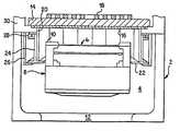
- An example of a single wafer vacuum processing chamber 2 having an inductively coupled plasma sourceis shown in FIG. 1 wherein processing gas is supplied to the processing chamber 2 by suitable apparatus (not shown) such as gas distribution rings, gas distribution plate, injection nozzles, etc., and a vacuum is maintained in the interior 4 of the chamber by suitable vacuum pump apparatus.
- the substrate to be processed in the chambercan comprise a silicon semiconductor wafer 6 supported on a substrate support 8 .
- the substrate support 8can include an electrostatic chuck and a focus ring 10 .
- the vacuum pumpcan be connected to a large outlet port 12 in an endwall such as the bottom of process chamber.
- the vacuum processing chambercan include a dielectric window 14 , a gas distribution plate 16 and RF power can be supplied to the chamber through an external RF antenna such as a planar coil 18 outside the dielectric window 14 on an endwall such as the top of the chamber.
- the plasma generating sourcecan be of any other type of plasma generating equipment such as that of an ECR reactor, a capacitively coupled parallel plate reactor, a surface wave reactor, a magnetron reactor, helicon reactor, helical resonator, etc.
- the plasma generating sourcecan be attached to a modular mounting arrangement such as an annular mounting flange which is removably mounted on the endwall of the chamber.
- suitable O-ring sealscan be fitted within grooves in the endwall of the chamber 2 and RF shielding members can surround the vacuum seals. If a large vacuum force is provided by the vacuum pump, it is not necessary to utilize fasteners for attaching the mounting flange to the chamber 2 . Instead, the mounting flange can simply rest on the endwall of the chamber 2 . If desired, the mounting flange or another part of the plasma generating source assembly can be hinged to the chamber 2 such that the plasma generating source can be pivoted to an orientation such as a vertical orientation for servicing the interior 4 of the chamber 2 .
- the chamberincludes a liner 20 , a plasma screen 22 for confining the plasma in the space surrounding the wafer 6 extends inwardly from the lower end of the liner 20 and a wafer passage insert 21 .
- the liner 20can be supported in any suitable way such as by an elastically bendable frame in the case of a solid cylindrical liner which includes an inner support frame 24 and an outer support frame 26 .
- a heater 28can be provided on the top of the inner frame support 24 . In operation, the heater 28 is effective to heat the liner 20 and removal of heat from the liner 20 can be accomplished by a temperature controlled member 30 which withdraws heat from the liner through the inner and outer frames.
- Other types of heating arrangementssuch as a heater embedded in the liner or suitable radiant heating arrangements can also be used.
- the chambercan have a modular design which allows various plasma generating sources to be mounted thereon.
- the substrate support 8can be supported at one end of a support arm mounted in a cantilever fashion such that the entire substrate support/support arm assembly can be removed from the chamber by passing the assembly through an opening 32 in the sidewall of the chamber.
- the chambercan be of any suitable material and according to a preferred embodiment of the invention the chamber is formed out of a single piece of aluminum or an aluminum alloy.
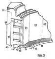
- the plasma chamber liner 20comprises interlocking ceramic liner elements such as flat tiles 34 , as shown in FIGS. 3 and 4.
- the tiles 34are preferably of an electrically conductive material such as silicon and carbon.
- the tilescan be entirely of CVD SiC or Si impregnated SiC coated with CVD SiC.
- Such a materialprovides an added benefit in that it does not contain aluminum and thus reduces Al contamination of processed substrates.
- the SiC tilescan be bonded to an aluminum backing plate 36 using an electrically conductive elastomer 38 which can absorb lateral stresses caused by different thermal expansion coefficients of the SiC and Al.
- Each tile and backing plate assemblycan be attached directly or indirectly to the chamber wall.
- the tilescan be supported by a support frame 40 which includes an inner frame 42 and an outer frame 44 . Temperature control of the liner can be achieved by a heater 48 supplied power by electrical leads 49 and a temperature controlled member 50 .
- the elastomeric jointcan comprise any suitable elastomeric material such as a polymer material compatible with a vacuum environment and resistant to thermal degradation at high temperatures such as above 200° C.
- the elastomer materialcan optionally include a filler of electrically and/or thermally conductive particles or other shaped filler such as wire mesh, woven or non-woven conductive fabric, etc.
- Polymeric materials which can be used in plasma environments above 160° C.include polyimide, polyketone, polyetherketone, polyether sulfone, polyethylene terephthalate, fluoroethylene propylene copolymers, cellulose, triacetates, silicone, and rubber.
- high purity elastomeric materialsinclude one-component room temperature curing adhesives available from General Electric as RTV 133 and RTV 167, a one-component flowable heat-curable (e.g. over 100° C.) adhesive available from General Electric as TSE 3221, and a two-part addition cure elastomer available from Dow Corning as “SILASTIC.”
- An especially preferred elastomeris a polydimethylsiloxane containing elastomer such as a catalyst cured, e.g. Pt-cured, elastomer available from Rhodia as V217, an elastomer stable at temperatures of 250° C. and higher.
- the electrically conductive filler materialcan comprise particles of a an electrically conductive metal or metal alloy.
- a preferred metal for use in the impurity sensitive environment of a plasma reaction chamberis an aluminum alloy such as a 5-20 weight % silicon containing aluminum base alloy.
- the aluminum alloycan include about 15 wt % silicon.
- filler particles of silicon or silicon carbidecan also be used.
- a plasma screen 52extends inwardly from a lower edge of the tiles 34 .
- the plasma screen 52is preferably of an electrically conductive ceramic material such as Si impregnated SiC coated with CVD SiC and includes openings 54 which are small enough to confine the plasma but allow process gas and processing byproducts to be removed by the vacuum pump.
- the heater 48can comprise an electrical resistance heating, element embedded in an aluminum casting.
- heatwill be supplied to the aluminum casting which in turn conducts heat into the inner frame 42 , the aluminum backing plates 36 , the heat conductive elastomer 38 and into the tiles 34 .
- the heaterwill expand to a greater extent than the ceramic liner formed by the tiles 34 .
- the inner and outer support framesare configured to be elastically bendable.
- the framescan be segmented such that a series of axially extending lower portions thereof are separated by axially extending slits.
- the inner and outer framescan be configured to provide a desired amount of thermal conductance.
- the outer frame 44can be of a metal such as aluminum or an aluminum alloy and a lower portion thereof can have a thickness sufficient to withdraw heat from the liner and a thin upper portion to allow adequate bending of the outer frame due to thermal stresses during processing of a semiconductor substrate.
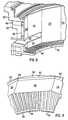
- FIG. 5shows a portion of the chamber wall wherein a substrate such as a wafer can be introduced and removed from the chamber through a transport slot 55 in a wafer passage insert.
- a substratesuch as a wafer
- some of the tiles 34are shorter in the axial direction in the vicinity of the slot 55 .
- the slot 55is preferably formed from an integral piece of Si impregnated SiC coated with CVD SiC.
- each tile 34can have edges 56 which interlock with mating edges of adjacent tiles, as shown in FIG. 6.
- the chamber 58can have polygonal inner surfaces 60 wherein the tiles are bonded directly to flat surfaces 60 of the chamber by an electrically and thermally conductive elastomer.
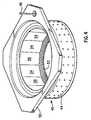
- FIG. 7shows a perspective view of a slip cast wafer passage insert 70 .
- the insert 70includes an inner surface 72 forming the wafer transfer slot 55 shown in FIG. 5.
- the shape of the part shown in FIG. 7can be slip cast in the manner described above and the inner surface 72 and optionally the entire outer surface 74 can be coated with CVD SiC.
- the side of the insert facing the interior of the plasma chamberincludes rectilinear edges 76 which abut surfaces of the tiles 34 opposite to the side of the tiles facing the interior of the chamber.
- FIG. 8shows a top view of the insert 70 and
- FIG. 9is an enlarged view of a corner 78 of one of the edges 76 , the edge 78 including an angled section 79 having a length corresponding to the wall thickness of insert 70 .
- the plasma in the chambercan be confined by the SiC surfaces of the gas distribution plate, the liner, the plasma screen and the substrate support which extends upwardly through the inner periphery of the plasma screen. Because the CVD coating on the Si impregnated SiC parts are located between the plasma and aluminum surfaces of the chamber, sputtering of the Al surfaces by the plasma is minimized and contaminating processed wafers with Al is reduced compared to chambers having Al surfaces with line-of-sight to the processed wafer.
- the linercomprises tiles of Si impregnated SiC coated with CVD SiC bonded to an aluminum backing plate by an electrically and/or thermally conductive elastomer bonding material.
- the linercan comprise a continuous surface rather than the individual tiles.
- the chamber wallcan be of any desired configuration such as cylindrical, polygonal, etc.
- a suitable access opening in the wafer passage insertallows passage of individual wafers into and out of the chamber and additional openings can be provided in Si impregnated SiC parts coated with CVD SiC to allow various measurements to be made by conventional accessories such as process monitoring equipment.
- the tilescan have a flat rectangular surface facing the interior of the chamber. Alternatively, the exposed surface of the tiles can be curved such that the tiles form a cylindrical inner wall of the chamber.
- the thermal stresses generated during start-up, operation and shut-down of the plasma chambercan be accommodated.
- the number of SiC tilescan be chosen to achieve a desired limit on part and/or bond stresses generated due to thermal forces encountered in the plasma chamber.
- the outer supportis segmented into vertically extending plates separated by slots which extend from the lower end of the outer support frame to the top flange.
- a heater located above the top flange of the inner support framecan be bolted to the inner frame. With such an arrangement, the heater can generate heat which is thermally conducted from the inner support frame to the backing plate and SiC tile.
- the heatercan comprise a single resistance heater which extends entirely around the inner wall of the chamber.
- the heatercan comprise any suitable heater arrangement which achieves the desired temperature control of the liner, e.g., maintaining the inner surface of the liner at a desired temperature such as in the range of 80 to 160° C. during plasma etching of dielectric materials such as silicon oxide.
- the chambercan include a plasma screen surrounding the substrate support.
- the annular screencan be attached to a carrier ring by any suitable technique.
- the screencan be adhesively bonded to the carrier ring by the elastomer bonding material discussed earlier.
- the carrier ringcan be bolted to a lower flange on the inner frame such that the screen is clamped between the carrier ring and the flange.
- the screencan be of any suitable material which will withstand a plasma environment for semiconductor production. Silicon carbide is a preferred material for the screen.
- the screencan comprise a single unitary ring or a plurality of spaced apart ring segments. For instance, the screen can include circumferentially spaced apart segments.
- the inner and outer framesinclude cut-outs therein and the tiles surrounding wafer transfer the slot are arranged such that smaller tiles are below the slot and larger tiles are above the slot.
- the wafer passage insertpreferably comprises a single piece of slip cast SiC which is impregnated with Si and then coated with CVD SiC. If desired, the insert can be made from an assembly of several pieces of such material.
- the edges of the tilesare preferably designed such that they overlap each other.
- the tilescan have mating edges wherein a projection on one tile is received in a recess in an adjacent tile. This effect can be obtained by any edge design wherein a rectilinear path is not provided between the opposed surfaces of the tile.
- a mating curved or multi-sided edge surfacesuch as a V-shaped, U-shaped, W-shaped, groove-shaped, notch-shaped, offset-shaped, etc. type edge can provide the desired mating tile edge.
- the interlocking tile jointseliminate line-of-sight to aluminum components and accommodate differential thermal expansion/contraction of liner components during startup, operation and/or shutdown of the plasma reactor. For instance, heat from the heater and/or plasma ion thermal energy deposited on the tiles is thermally conducted by the inner frame, through the elastomer bond, up the outer frame and into the chamber top plate. Due to water cooling of the top plate via cooling channels, the heat transferred through outer frame is removed from the chamber.
- the tilescan be preheated by the heater before plasma is generated in the chamber.
- the tilescan be heated to a desired temperature by the heater and a thermal control system can be used to adjust the heater power to maintain the tiles at the desired temperature.
- the control systemcan automatically reduce the heater power to maintain the desired time temperature.
- the thermal impedances of the inner and/or outer framescan be adjusted to achieve the desired range of tile operating temperatures and limit the heater maximum temperature.
- a resistance heatercan be used to heat the ceramic liner by thermal conduction, i.e., heat from the heater passes through a resilient Al frame to the ceramic liner. In such an arrangement, the heater and part of the Al frame in contact therewith may heat to around 300° C.
- the resilient Al framecomprised of the inner and outer frames allows the part of the Al frame in contact with the heater to expand relative to the portion of the Al frame in contact with the ceramic liner and thus accommodate any bending stresses on the intermediate part of the Al frame.
- one or more parts of the chambercan be made of CVD SiC.
- the CVD SiCcan be deposited on a substrate such as graphite and grown to a desired thickness after which the substrate is removed such as by machining.
- CVD SiCcan be deposited to a desired thickness on a graphite cylinder and the graphite cylinder is later machined away leaving the CVD SiC cylinder liner.
- Advantages of the CVD SiCinclude high thermal conductivity (e.g., CVD SiC has about twice as much thermal conductivity as sintered SiC) and tailored electrical resistivity (e.g., resistivity of SiC can be varied from electrically conducting to semiconducting).
- An advantage of using CVD SiC for the reactor componentsis that it is possible to obtain a highly uniform temperature distribution across the surface of the component inside the reactor.
- the use of CVD SiCis highly advantageous from the standpoint of temperature control and minimizing particle generation.
- a mixture of 1 part by weight of medium particles of SiC powder with average particle diameters between 10 ⁇ m and 30 ⁇ m and 1-2.5 parts by weight of coarse particles of SiC powder with average particle diameters between 80 ⁇ m and 200 ⁇ mis kneaded and granulated after adding an organic binding agent. Then, the mixture is formed into a shape defined by a plaster mold after which the shaped part is dried. Next, the shaped part is presintered at 800 to 1200° C. followed by reaction sintering at 1500 to 1800° C. while impregnating the shaped part with Si.
- the sintered partis then placed in a vacuum furnace and coated with SiC using a mixture of trichloromethyl silane gas at 4 ml/min with hydrogen as a carrier gas at 4000 ml/min.
- a slip cast SiC partis produced with a CVD SiC coating.
Landscapes
- Engineering & Computer Science (AREA)
- Physics & Mathematics (AREA)
- Plasma & Fusion (AREA)
- Chemical & Material Sciences (AREA)
- Analytical Chemistry (AREA)
- General Physics & Mathematics (AREA)
- Condensed Matter Physics & Semiconductors (AREA)
- Manufacturing & Machinery (AREA)
- Computer Hardware Design (AREA)
- Microelectronics & Electronic Packaging (AREA)
- Power Engineering (AREA)
- Drying Of Semiconductors (AREA)
- Chemical Vapour Deposition (AREA)
Abstract
Description
- The invention relates to semiconductor processing equipment and more particularly to improved process drift control during processing such as plasma etching of semiconductor substrates.[0001]
- In the field of semiconductor processing, vacuum processing chambers are generally used for etching and chemical vapor deposition (CVD) of materials on substrates by supplying an etching or deposition gas to the vacuum chamber and application of an RF field to the gas to energize the gas into a plasma state. Examples of parallel plate, transformer coupled plasma (TCP™) which is also called inductively coupled plasma (ICP), and electron-cyclotron resonance (ECR) reactors and components thereof are disclosed in commonly owned U.S. Pat. Nos. 4,340,462; 4,948,458; 5,200,232 and 5,820,723. Because of the corrosive nature of the plasma environment in such reactors and the requirement for minimizing particle and/or heavy metal contamination, it is highly desirable for the components of such equipment to exhibit high corrosion resistance.[0002]
- During processing of semiconductor substrates, the substrates are typically held in place within the vacuum chamber on substrate holders by mechanical clamps and electrostatic clamps (ESC). Examples of such clamping systems and components thereof can be found in commonly owned U.S. Pat. Nos. 5,262,029 and 5,838,529. Process gas can be supplied to the chamber in various ways such as by gas nozzles, gas rings, gas distribution plates, etc. An example of a temperature controlled gas distribution plate for an inductively coupled plasma reactor and components thereof can be found in commonly owned U.S. Pat. No. 5,863,376.[0003]
- Aluminum and aluminum alloys are commonly used for walls of plasma reactors. In order to prevent corrosion of the walls, various techniques have been proposed for coating the aluminum surface with various coatings. For instance, U.S. Pat. No. 5,641,375 discloses that aluminum chamber walls have been anodized to reduce plasma erosion and wear of the walls. The '375 patent states that eventually the anodized layer is sputtered or etched off and the chamber must be replaced. U.S. Pat. No. 5,680,013 states that a technique for flame spraying Al[0004]2O3on metal surfaces of an etching chamber is disclosed in U.S. Pat. No. 4,491,496. The '013 patent states that the differences in thermal expansion coefficients between aluminum and ceramic coatings such as aluminum oxide leads to cracking of the coatings due to thermal cycling and eventual failure of the coatings in corrosive environments. U.S. Pat. No. 5,085,727 discloses a carbon coating for walls of a plasma chamber wherein the coating is deposited by plasma assisted CVD.
- In order to protect the chamber walls, U.S. Pat. Nos. 5,366,585; 5,556,501; 5,788,799; 5,798,016; and 5,885,356 propose liner arrangements. For instance, the '585 patent discloses a free standing ceramic liner having a thickness of at least 0.005 inches and machined from solid alumina. The '585 patent also mentions use of ceramic layers which are deposited without consuming the underlying aluminum can be provided by flame sprayed or plasma sprayed aluminum oxide. The '501 patent discloses a process-compatible liner of polymer or quartz or ceramic. The '799 patent discloses a temperature controlled ceramic liner having a resistance heater embedded therein and the ceramic can be alumina, silica, titania, zirconia, silicon carbide, titanium carbide, zirconium carbide, aluminum nitride, boron nitride, silicon nitride and titanium nitride. The '016 patent discloses a liner of ceramics, aluminum, steel and/or quartz with aluminum being preferred for its ease of machinability and having a coating of aluminum oxide, Sc[0005]2O3or Y2O3, with Al2O3being preferred for coating aluminum to provide protection of the aluminum from plasma. The '356 patent discloses a ceramic liner of alumina and a ceramic shield of aluminum nitride for the wafer pedestal for use in CVD chambers.
- U.S. Pat. No. 5,904,778 discloses a SiC CVD coating on free standing SiC for use as a chamber wall, chamber roof, or collar around the wafer. U.S. Pat. No. 5,292,399 discloses a SiC ring surrounding a wafer pedestal. A technique for preparing sintered SiC is disclosed in U.S. Pat. No. 5,182,059.[0006]
- In addition to the above, the use of silicon carbide in semiconductor processing equipment is disclosed in U.S. Pat. No. 4,401,689 (susceptor tube), U.S. Pat. No. 4,518,349 (furnace support rod), U.S. Pat. No. 4,999,228 (diffusion tube), U.S. Pat. No. 5,074,456 (upper electrode), U.S. Pat. No. 5,252,892 (plasma cathode chamber), U.S. Pat. No. 5,460,684 (resistive layer of ESC), U.S. Pat. No. 5,463,524 (sensing pin), U.S. Pat. No. 5,578,129 (filter plate of load lock system), U.S. Pat. No. 5,538,230 (wafer boat), U.S. Pat. No. 5,595,627 (upper electrode), U.S. Pat. No. 5,888,907 (electrode plate), and U.S. Pat. No. 5,892,236 (ion implantation device).[0007]
- Other documents include Japanese Pat. Publication Nos. 54-10825 (semiconductor diffusion oven material), 60-200519 (susceptor), 61-284301 (upper electrode), 63-35452 (diffusion oven tube, liner tube, port element, paddle), 63-186874 (microwave heated sample plate), 63-138737 (upper electrode of plasma etch reactor), 3-201322 (coating for part in vacuum environment), and 8-17745 (wafer heater). Of these, Japanese Pat. Publication Nos. 54-10825 and 63-35452 disclose parts made of slip cast silicon carbide.[0008]
- With regard to plasma reactor components such as showerhead gas distribution systems, various proposals have been made with respect to the materials of the showerheads. For instance, commonly owned U.S. Pat. No. 5,569,356 discloses a showerhead of silicon, graphite, or silicon carbide. U.S. Pat. No. 5,888,907 discloses a showerhead electrode of amorphous carbon, SiC or Al. U.S. Pat. Nos. 5,006,220 and 5,022,979 disclose a showerhead electrode either made entirely of SiC or a base of carbon coated with SiC deposited by CVD to provide a surface layer of highly pure SiC.[0009]
- In discussing the need for cleanliness and the elimination of contaminants in the processing of semiconductor wafers, U.S. Pat. No. 5,538,230 references U.S. Pat. Nos. 3,951,541; 3,962,391; 4,093,201; 4,203,940; 4,761,134; 4,978,567; 4,987,016 and Japanese Publication No. 50-90184. The '230 patent also references U.S. Pat. Nos. 3,951,587 and 5,283,089 for discussions of SiC parts and references U.S. Pat. No. 4,761,134 for a discussion of CVD SiC on Si infiltrated SiC or porous Si that has not been filled with Si.[0010]
- Japanese Publication No. 63-273323 discloses SiC parts for an ECR plasma deposition apparatus wherein silicon dioxide is deposited on samples, the SiC parts being coated with SiC by generating a plasma in the chamber and introducing methane and silane gases into the chamber.[0011]
- In view of the need for high purity and corrosion resistance for components of semiconductor processing equipment, there is a need in the art for improvements in materials and/or coatings used for such components. Moreover, with regard to the chamber materials, any materials which can increase the service life of a plasma reactor chamber and thus reduce the down time of the apparatus, would be beneficial in reducing the cost of processing the semiconductor wafers.[0012]
- The invention provides a method of processing semiconductor substrates and reducing particle contamination and/or process drift during consecutive processing of the substrates. The method comprising steps of (a) placing a substrate on a substrate holder in an interior space of a plasma processing chamber, the processing chamber including at lease one slip cast part having a surface exposed to the interior space, the slip cast part having free silicon contained therein and a protective layer on the surface which protects the silicon from being attacked by the plasma in the interior space, (b) processing the substrate by supplying process gas to the processing chamber and energizing the process gas into a plasma state in the processing chamber, the slip cast part being exposed to the plasma and optionally providing a ground path for RF current sustaining the plasma, (c) removing the substrate from the processing chamber, and (d) consecutively processing additional substrates in the processing chamber by repeating steps (a-c) while minimizing particle contamination of the substrates and/or reducing process drift during the processing step as a result of protecting the free silicon from attack by the plasma.[0013]
- According to one optional aspect of the method, the slip cast part can comprise a liner within a sidewall of the processing chamber and the processing chamber can include a substantially planar antenna which energizes the process gas into the plasma state by supplying RF power to the antenna. For plasma etching of oxide materials, the process gas can comprise one or more hydrofluorocarbon gases. For oxide etching, the plasma preferably comprises a high density plasma which etches an oxide layer on the substrates while an RF bias is applied to the substrates.[0014]
- The slip cast part can comprise one or more parts of the chamber. For instance, the slip cast part can comprise a liner within a sidewall of the processing chamber, a gas distribution plate supplying the process gas to the processing chamber, a perforated baffle extending between the substrate holder and an inner wall of the processing chamber, a wafer passage insert, a focus ring surrounding the substrate, a tubular liner protecting a process monitoring device, or the like. In a preferred embodiment, the slip cast part is a wafer passage insert fitted in an opening in a ceramic liner within a sidewall of the processing chamber wherein the liner is heated by a heater which maintains the liner at a desired temperature. The slip cast part can consist essentially of silicon impregnated slip cast SiC coated with CVD SiC.[0015]
- In an exemplary process, a first slip cast part comprises a heated liner and a second slip cast part comprises a plasma screen arranged such that the liner surrounds the substrate holder and the plasma screen extends between the liner and the substrate holder, the liner being heated to a temperature above room temperature during the processing step. In another process, the slip cast part comprises a gas distribution plate having a resistivity high enough to pass RF energy therethrough, the process gas being energized by an antenna which couples RF energy into the chamber through the gas distribution plate. A third slip cast part can comprise a chamber liner having a resistivity below 200 Ω·cm, preferably below 50 Ω·cm, and more preferably below 10 Ω·cm.[0016]
- The invention also provides a plasma processing system useful for processing semiconductor substrates comprising a plasma processing chamber having an interior space bounded by a chamber sidewall, a substrate support on which a substrate is processed within the interior space arranged such that the chamber sidewall is spaced outwardly of a periphery of the substrate support, a gas supply through which process gas can be supplied to the interior space during processing of the substrate, an energy source which can energize the process gas in the interior space into a plasma state during processing of the substrate, and a slip cast part having a surface thereof exposed to the interior space, the slip cast part having free silicon contained therein and a protective layer on the surface which protects the silicon from being attacked by the plasma in the interior space. According to a preferred embodiment, the slip cast part is of porous silicon carbide backfilled with silicon and the protective layer is a chemical vapor deposited layer of silicon carbide. A preferred slip cast part is a wafer passage insert of a plasma etch reactor wherein the gas supply supplies a fluorocarbon and/or a fluorohydrocarbon to the interior space.[0017]
- In a less preferred embodiment, the slip cast part is bonded to the chamber by an elastomer joint or the chamber can include a ceramic liner between the chamber sidewall and the substrate support wherein the slip cast part comprises a tubular liner in an opening extending through the liner. A preferred energy source is an antenna such as a planar coil which inductively couples radiofrequency energy through a dielectric member into the chamber.[0018]
- According to a preferred embodiment, the interior of the chamber is bounded by a showerhead having a silicon carbide surface extending across the top of the chamber, a liner having a silicon carbide surface extending downwardly from the silicon carbide surface of the showerhead, a plasma screen having a silicon carbide surface extending inwardly from the silicon carbide surface of the liner, and the slip cast part comprises a wafer passage insert fitted in an opening in the liner, the CVD SiC coating forming a surface of the wafer passage insert through which a semiconductor wafer passes into and out of the chamber.[0019]
- FIG. 1 shows a single wafer vacuum processing chamber having an inductively coupled plasma source and a tiled liner of slip cast parts in accordance with the invention;[0020]
- FIG. 2 shows the plasma reaction chamber of FIG. 1 without various components including the tiled liner;[0021]
- FIG. 3 shows details of a support arrangement for the tiled liner;[0022]
- FIG. 4 shows a perspective view of the plasma chamber of FIG. 3;[0023]
- FIG. 5 shows details of a slip cast wafer passage insert in accordance with the invention;[0024]
- FIG. 6 shows how edges of the tiles of FIG. 3 fit together in an interlocking arrangement;[0025]
- FIG. 7 shows a perspective view of a one piece slip cast wafer passage insert in accordance with the invention;[0026]
- FIG. 8 shows a top view of the insert shown in FIG. 7; and[0027]
- FIG. 9 shows an enlarged view of a corner of the insert shown in FIG. 8.[0028]
- According to the invention, a plasma processing chamber having improved process drift control is provided. The improved process drift control is achieved by use of one or more parts in the chamber of a part having a surface thereof exposed to the interior space, the part having free silicon contained therein and a protective layer on the surface which protects the silicon from being attacked by the plasma in the interior. The free silicon can be silicon impregnated into a porous SiC body, the silicon filling the porosity to minimize undesirable process effects and increase electrical conductivity which is useful for lowering the RF impedance of the part.[0029]
- The part can have any desired configuration such as that of a wafer passage insert, a chamber wall, a substrate support, an electrode, a showerhead, etc. According to a preferred embodiment, the part comprises a slip cast silicon carbide part which has been backfilled or impregnated with silicon and the protective coating preferably comprises CVD silicon carbide.[0030]
- The invention provides parts for a plasma chamber wherein the parts are made entirely of Si and SiC. Such materials are compatible in plasma environments since plasma erosion of Si or SiC produces gaseous Si or C compounds which can be pumped from the chamber without particle contamination of the substrate. With regard to thermal control, SiC has been found to exhibit exceptionally high thermal conductivity enabling parts of such material to be heated or cooled to a desired temperature range during processing of substrates such as silicon wafers.[0031]
- Slip cast SiC parts in accordance with the invention can be made by the following process. In the process, a bimodal distribution of SiC powder is prepared. For example, a first SiC fraction having a mean particle size of 10 to 80 μm, preferably 25 to 50 μm is combined with a second fraction having a mean particle size of 80 to 200 μm, preferably 100 to 150 μm, the powder mixture is combined with water and organic agents such as a flocculent, and the mixture is poured into a mold to form a slip cast part. After drying such as at room temperature, the slip cast part is green machined and sintered at a suitable temperature such as around 1500 to 2000° C., the sintered part is purified in an acid bath, the cleaned part is subjected to impregnation with silicon to fill the porosity (e.g., 15 to 20%) of the part such as by melting powdered silicon and wicking the melted silicon through porous graphite and into the part fill essentially 100% of the porosity in the part, cooling the part followed by removing any excess silicon exuded out of the part, and machining the part to final tolerances such as by diamond grinding. The surface of the part can be sealed with a CVD SiC coating of any suitable thickness such as 50 to 500 μm, preferably around 200 μm for parts not directly exposed to the plasma or the coating can be in excess of 1 mm, preferably 2 mm or more for parts exposed directly to the plasma.[0032]
- The slip cast part can be used in any plasma reaction chamber wherein it is desired to reduce particle contamination and/or reduce process drift. An example of a single wafer[0033]
vacuum processing chamber 2 having an inductively coupled plasma source is shown in FIG. 1 wherein processing gas is supplied to theprocessing chamber 2 by suitable apparatus (not shown) such as gas distribution rings, gas distribution plate, injection nozzles, etc., and a vacuum is maintained in theinterior 4 of the chamber by suitable vacuum pump apparatus. The substrate to be processed in the chamber can comprise a silicon semiconductor wafer6 supported on a substrate support8. The substrate support8 can include an electrostatic chuck and afocus ring 10. The vacuum pump can be connected to alarge outlet port 12 in an endwall such as the bottom of process chamber. The vacuum processing chamber can include adielectric window 14, agas distribution plate 16 and RF power can be supplied to the chamber through an external RF antenna such as aplanar coil 18 outside thedielectric window 14 on an endwall such as the top of the chamber. However, the plasma generating source can be of any other type of plasma generating equipment such as that of an ECR reactor, a capacitively coupled parallel plate reactor, a surface wave reactor, a magnetron reactor, helicon reactor, helical resonator, etc. The plasma generating source can be attached to a modular mounting arrangement such as an annular mounting flange which is removably mounted on the endwall of the chamber. - In order to maintain a vacuum tight seal between the mounting flange and the[0034]
chamber 2, suitable O-ring seals can be fitted within grooves in the endwall of thechamber 2 and RF shielding members can surround the vacuum seals. If a large vacuum force is provided by the vacuum pump, it is not necessary to utilize fasteners for attaching the mounting flange to thechamber 2. Instead, the mounting flange can simply rest on the endwall of thechamber 2. If desired, the mounting flange or another part of the plasma generating source assembly can be hinged to thechamber 2 such that the plasma generating source can be pivoted to an orientation such as a vertical orientation for servicing theinterior 4 of thechamber 2. - The chamber includes a[0035]
liner 20, aplasma screen 22 for confining the plasma in the space surrounding the wafer6 extends inwardly from the lower end of theliner 20 and awafer passage insert 21. Theliner 20 can be supported in any suitable way such as by an elastically bendable frame in the case of a solid cylindrical liner which includes aninner support frame 24 and anouter support frame 26. In order to maintain the liner at a desired temperature during processing of a substrate, aheater 28 can be provided on the top of theinner frame support 24. In operation, theheater 28 is effective to heat theliner 20 and removal of heat from theliner 20 can be accomplished by a temperature controlledmember 30 which withdraws heat from the liner through the inner and outer frames. Other types of heating arrangements such as a heater embedded in the liner or suitable radiant heating arrangements can also be used. - As shown in FIG. 2, the chamber can have a modular design which allows various plasma generating sources to be mounted thereon. Further, the substrate support[0036]8 can be supported at one end of a support arm mounted in a cantilever fashion such that the entire substrate support/support arm assembly can be removed from the chamber by passing the assembly through an
opening 32 in the sidewall of the chamber. The chamber can be of any suitable material and according to a preferred embodiment of the invention the chamber is formed out of a single piece of aluminum or an aluminum alloy. - According to a first embodiment of the invention, the[0037]
plasma chamber liner 20 comprises interlocking ceramic liner elements such asflat tiles 34, as shown in FIGS. 3 and 4. To provide an electrical ground path for the plasma, thetiles 34 are preferably of an electrically conductive material such as silicon and carbon. For example, the tiles can be entirely of CVD SiC or Si impregnated SiC coated with CVD SiC. Such a material provides an added benefit in that it does not contain aluminum and thus reduces Al contamination of processed substrates. The SiC tiles can be bonded to analuminum backing plate 36 using an electricallyconductive elastomer 38 which can absorb lateral stresses caused by different thermal expansion coefficients of the SiC and Al. Each tile and backing plate assembly can be attached directly or indirectly to the chamber wall. For example, the tiles can be supported by asupport frame 40 which includes aninner frame 42 and anouter frame 44. Temperature control of the liner can be achieved by aheater 48 supplied power byelectrical leads 49 and a temperature controlledmember 50. - The elastomeric joint can comprise any suitable elastomeric material such as a polymer material compatible with a vacuum environment and resistant to thermal degradation at high temperatures such as above 200° C. The elastomer material can optionally include a filler of electrically and/or thermally conductive particles or other shaped filler such as wire mesh, woven or non-woven conductive fabric, etc. Polymeric materials which can be used in plasma environments above 160° C. include polyimide, polyketone, polyetherketone, polyether sulfone, polyethylene terephthalate, fluoroethylene propylene copolymers, cellulose, triacetates, silicone, and rubber. Examples of high purity elastomeric materials include one-component room temperature curing adhesives available from General Electric as RTV 133 and RTV 167, a one-component flowable heat-curable (e.g. over 100° C.) adhesive available from General Electric as TSE 3221, and a two-part addition cure elastomer available from Dow Corning as “SILASTIC.” An especially preferred elastomer is a polydimethylsiloxane containing elastomer such as a catalyst cured, e.g. Pt-cured, elastomer available from Rhodia as V217, an elastomer stable at temperatures of 250° C. and higher.[0038]
- In the case where the elastomer is an electrically conductive elastomer, the electrically conductive filler material can comprise particles of a an electrically conductive metal or metal alloy. A preferred metal for use in the impurity sensitive environment of a plasma reaction chamber is an aluminum alloy such as a 5-20 weight % silicon containing aluminum base alloy. For example, the aluminum alloy can include about 15 wt % silicon. However, filler particles of silicon or silicon carbide can also be used.[0039]
- A[0040]
plasma screen 52 extends inwardly from a lower edge of thetiles 34. Theplasma screen 52 is preferably of an electrically conductive ceramic material such as Si impregnated SiC coated with CVD SiC and includesopenings 54 which are small enough to confine the plasma but allow process gas and processing byproducts to be removed by the vacuum pump. - The[0041]
heater 48 can comprise an electrical resistance heating, element embedded in an aluminum casting. Thus, by passing electrical current through the heating element, heat will be supplied to the aluminum casting which in turn conducts heat into theinner frame 42, thealuminum backing plates 36, the heatconductive elastomer 38 and into thetiles 34. During heating and cooling of the aluminum body of the heater, the heater will expand to a greater extent than the ceramic liner formed by thetiles 34. In order to accommodate such expansion and contraction, the inner and outer support frames are configured to be elastically bendable. For example, the frames can be segmented such that a series of axially extending lower portions thereof are separated by axially extending slits. In addition, the inner and outer frames can be configured to provide a desired amount of thermal conductance. For instance, theouter frame 44 can be of a metal such as aluminum or an aluminum alloy and a lower portion thereof can have a thickness sufficient to withdraw heat from the liner and a thin upper portion to allow adequate bending of the outer frame due to thermal stresses during processing of a semiconductor substrate. - FIG. 5 shows a portion of the chamber wall wherein a substrate such as a wafer can be introduced and removed from the chamber through a[0042]
transport slot 55 in a wafer passage insert. In the arrangement shown in FIG. 5, some of thetiles 34 are shorter in the axial direction in the vicinity of theslot 55. Theslot 55 is preferably formed from an integral piece of Si impregnated SiC coated with CVD SiC. - In order to prevent a line of sight between the wafer[0043]6 and the
chamber wall 46, eachtile 34 can haveedges 56 which interlock with mating edges of adjacent tiles, as shown in FIG. 6. As shown in this alternative embodiment, thechamber 58 can have polygonalinner surfaces 60 wherein the tiles are bonded directly toflat surfaces 60 of the chamber by an electrically and thermally conductive elastomer. Such an arrangement is advantageous in that it has fewer parts than the tile/backing plate arrangement and allows liner removal for cleaning and replacement to be carried out more quickly. - FIG. 7 shows a perspective view of a slip cast[0044]
wafer passage insert 70. Theinsert 70 includes aninner surface 72 forming thewafer transfer slot 55 shown in FIG. 5. The shape of the part shown in FIG. 7 can be slip cast in the manner described above and theinner surface 72 and optionally the entireouter surface 74 can be coated with CVD SiC. The side of the insert facing the interior of the plasma chamber includesrectilinear edges 76 which abut surfaces of thetiles 34 opposite to the side of the tiles facing the interior of the chamber. FIG. 8 shows a top view of theinsert 70 and FIG. 9 is an enlarged view of acorner 78 of one of theedges 76, theedge 78 including anangled section 79 having a length corresponding to the wall thickness ofinsert 70. - In the foregoing embodiments, the plasma in the chamber can be confined by the SiC surfaces of the gas distribution plate, the liner, the plasma screen and the substrate support which extends upwardly through the inner periphery of the plasma screen. Because the CVD coating on the Si impregnated SiC parts are located between the plasma and aluminum surfaces of the chamber, sputtering of the Al surfaces by the plasma is minimized and contaminating processed wafers with Al is reduced compared to chambers having Al surfaces with line-of-sight to the processed wafer.[0045]
- In the foregoing embodiment, the liner comprises tiles of Si impregnated SiC coated with CVD SiC bonded to an aluminum backing plate by an electrically and/or thermally conductive elastomer bonding material. If desired, the liner can comprise a continuous surface rather than the individual tiles. The chamber wall can be of any desired configuration such as cylindrical, polygonal, etc. A suitable access opening in the wafer passage insert allows passage of individual wafers into and out of the chamber and additional openings can be provided in Si impregnated SiC parts coated with CVD SiC to allow various measurements to be made by conventional accessories such as process monitoring equipment. The tiles can have a flat rectangular surface facing the interior of the chamber. Alternatively, the exposed surface of the tiles can be curved such that the tiles form a cylindrical inner wall of the chamber.[0046]
- In the embodiment wherein the tile and backing plate assemblies are bolted to an Al inner support frame which extends around the inner wall of the chamber, the thermal stresses generated during start-up, operation and shut-down of the plasma chamber can be accommodated. The number of SiC tiles can be chosen to achieve a desired limit on part and/or bond stresses generated due to thermal forces encountered in the plasma chamber.[0047]
- In the embodiment wherein a lower flange of the inner support frame is bolted to the lower edge of an Al outer support frame and a flange at the upper edge of the outer support frame is bolted to a top plate located on top of the chamber, the outer support is segmented into vertically extending plates separated by slots which extend from the lower end of the outer support frame to the top flange. In order to provide temperature control of the SiC tiled surface, a heater located above the top flange of the inner support frame can be bolted to the inner frame. With such an arrangement, the heater can generate heat which is thermally conducted from the inner support frame to the backing plate and SiC tile. The heater can comprise a single resistance heater which extends entirely around the inner wall of the chamber. Alternatively, the heater can comprise any suitable heater arrangement which achieves the desired temperature control of the liner, e.g., maintaining the inner surface of the liner at a desired temperature such as in the range of 80 to 160° C. during plasma etching of dielectric materials such as silicon oxide.[0048]
- The chamber can include a plasma screen surrounding the substrate support. The annular screen can be attached to a carrier ring by any suitable technique. For instance, the screen can be adhesively bonded to the carrier ring by the elastomer bonding material discussed earlier. In addition, the carrier ring can be bolted to a lower flange on the inner frame such that the screen is clamped between the carrier ring and the flange. The screen can be of any suitable material which will withstand a plasma environment for semiconductor production. Silicon carbide is a preferred material for the screen. The screen can comprise a single unitary ring or a plurality of spaced apart ring segments. For instance, the screen can include circumferentially spaced apart segments.[0049]
- In order to accommodate the wafer passage insert, the inner and outer frames include cut-outs therein and the tiles surrounding wafer transfer the slot are arranged such that smaller tiles are below the slot and larger tiles are above the slot. The wafer passage insert preferably comprises a single piece of slip cast SiC which is impregnated with Si and then coated with CVD SiC. If desired, the insert can be made from an assembly of several pieces of such material.[0050]
- According to the embodiment of the invention wherein line-of-sight surfaces of aluminum components are avoided by covering the surfaces with the SiC tiles, the edges of the tiles are preferably designed such that they overlap each other. For instance, the tiles can have mating edges wherein a projection on one tile is received in a recess in an adjacent tile. This effect can be obtained by any edge design wherein a rectilinear path is not provided between the opposed surfaces of the tile. Thus, a mating curved or multi-sided edge surface such as a V-shaped, U-shaped, W-shaped, groove-shaped, notch-shaped, offset-shaped, etc. type edge can provide the desired mating tile edge.[0051]
- The interlocking tile joints eliminate line-of-sight to aluminum components and accommodate differential thermal expansion/contraction of liner components during startup, operation and/or shutdown of the plasma reactor. For instance, heat from the heater and/or plasma ion thermal energy deposited on the tiles is thermally conducted by the inner frame, through the elastomer bond, up the outer frame and into the chamber top plate. Due to water cooling of the top plate via cooling channels, the heat transferred through outer frame is removed from the chamber.[0052]
- During processing of semiconductor substrates, the tiles can be preheated by the heater before plasma is generated in the chamber. For instance, the tiles can be heated to a desired temperature by the heater and a thermal control system can be used to adjust the heater power to maintain the tiles at the desired temperature. After plasma is generated in the chamber, the control system can automatically reduce the heater power to maintain the desired time temperature. Further, the thermal impedances of the inner and/or outer frames can be adjusted to achieve the desired range of tile operating temperatures and limit the heater maximum temperature.[0053]
- During processing of semiconductor substrates such as plasma etching of silicon wafers, in order to minimize deposition of polymer from gaseous byproducts produced during the etching process, it is desirable to maintain chamber surfaces exposed to the plasma at temperatures of about 80° C. to about 160° C., preferably 110 to 150° C. In addition, such temperature control of these surfaces provides reduction in processing drift during sequential processing of individual wafers. Prior to striking a plasma in the chamber, a resistance heater can be used to heat the ceramic liner by thermal conduction, i.e., heat from the heater passes through a resilient Al frame to the ceramic liner. In such an arrangement, the heater and part of the Al frame in contact therewith may heat to around 300° C. in order to heat the ceramic liner to around 150° C. The resilient Al frame comprised of the inner and outer frames allows the part of the Al frame in contact with the heater to expand relative to the portion of the Al frame in contact with the ceramic liner and thus accommodate any bending stresses on the intermediate part of the Al frame.[0054]
- If desired, one or more parts of the chamber can be made of CVD SiC. The CVD SiC can be deposited on a substrate such as graphite and grown to a desired thickness after which the substrate is removed such as by machining. For example, in the case of a cylindrical liner, CVD SiC can be deposited to a desired thickness on a graphite cylinder and the graphite cylinder is later machined away leaving the CVD SiC cylinder liner. Advantages of the CVD SiC include high thermal conductivity (e.g., CVD SiC has about twice as much thermal conductivity as sintered SiC) and tailored electrical resistivity (e.g., resistivity of SiC can be varied from electrically conducting to semiconducting). An advantage of using CVD SiC for the reactor components is that it is possible to obtain a highly uniform temperature distribution across the surface of the component inside the reactor. In the case of processing wherein the component is maintained at a high enough temperature to minimize polymer buildup on the exposed surfaces of the component, the use of CVD SiC is highly advantageous from the standpoint of temperature control and minimizing particle generation.[0055]
- An example of preparing a slip cast component in accordance with the invention is as follows.[0056]
- A mixture of 1 part by weight of medium particles of SiC powder with average particle diameters between 10 μm and 30 μm and 1-2.5 parts by weight of coarse particles of SiC powder with average particle diameters between 80 μm and 200 μm is kneaded and granulated after adding an organic binding agent. Then, the mixture is formed into a shape defined by a plaster mold after which the shaped part is dried. Next, the shaped part is presintered at 800 to 1200° C. followed by reaction sintering at 1500 to 1800° C. while impregnating the shaped part with Si. The sintered part is then placed in a vacuum furnace and coated with SiC using a mixture of trichloromethyl silane gas at 4 ml/min with hydrogen as a carrier gas at 4000 ml/min. As a result, a slip cast SiC part is produced with a CVD SiC coating.[0057]
- The foregoing has described the principles, preferred embodiments and modes of operation of the present invention. However, the invention should not be construed as being limited to the particular embodiments discussed. Thus, the above-described embodiments should be regarded as illustrative rather than restrictive, and it should be appreciated that variations may be made in those embodiments by workers skilled in the art without departing from the scope of the present invention as defined by the following claims.[0058]
Claims (18)
1. A method of processing semiconductor substrates and reducing particle contamination and/or process drift during consecutive processing of the substrates, the method comprising steps of:
(a) placing a substrate on a substrate holder in an interior space of a plasma processing chamber, the processing chamber including at lease one slip cast part having a surface exposed to the interior space, the slip cast part having free silicon contained therein and a protective layer on the surface which protects the silicon from being attacked by the plasma in the interior space;
(b) processing the substrate by supplying process gas to the processing chamber and energizing the process gas into a plasma state in the processing chamber, the slip cast part being exposed to the plasma and optionally providing a ground path for RF current sustaining the plasma;
(c) removing the substrate from the processing chamber; and
(d) consecutively processing additional substrates in the processing chamber by repeating steps (a-c) while minimizing particle contamination of the substrates and/or reducing process drift during the processing step as a result of protecting the free silicon from attack by the plasma.
2. The method according toclaim 1 , wherein the slip cast part comprises a liner within a sidewall of the processing chamber, the processing chamber including a substantially planar antenna which energizes the process gas into the plasma state by supplying RF power to the antenna and the process gas comprising one or more hydrofluorocarbon gases.
3. The method according toclaim 1 , wherein the plasma comprises a high density plasma and the substrates are processed by etching an oxide layer on the substrates with the high density plasma while supplying an RF bias to the substrates.
4. The method according toclaim 1 , wherein the slip cast part comprises a liner within a sidewall of the processing chamber, a gas distribution plate supplying the process gas to the processing chamber, a perforated baffle extending between the substrate holder and an inner wall of the processing chamber, a wafer passage insert and/or a focus ring surrounding the substrate.
5. The method according toclaim 1 , wherein the slip cast part comprises a wafer passage insert fitted in an opening in a ceramic liner within a sidewall of the processing chamber, the liner being heated by a heater which maintains the liner at a desired temperature.
6. The method according toclaim 1 , wherein the slip cast part consists essentially of silicon impregnated slip cast SiC coated with CVD SiC.
7. The method according toclaim 1 , wherein the slip cast part comprises a heated liner and a baffle, the liner surrounding the substrate holder and the baffle comprising a foraminous ring extending between the liner and the substrate holder, the liner being heated to a temperature above room temperature during the processing step.
8. The method according toclaim 1 , wherein the slip cast part comprises a gas distribution plate having a resistivity high enough to allow RF energy to pass therethrough, the process gas being energized by an antenna which couples RF energy into the chamber through the gas distribution plate.
9. The method according toclaim 8 , wherein the slip cast part further comprises a chamber liner having a resistivity below 200 Ω·cm.
10. A plasma processing system useful for processing semiconductor substrates comprising:
a plasma processing chamber having an interior space bounded by a chamber sidewall;
a substrate support on which a substrate is processed within the interior space, the chamber sidewall being spaced outwardly of a periphery of the substrate support;
a gas supply through which process gas can be supplied to the interior space during processing of the substrate;
an energy source which can energize the process gas in the interior space into a plasma state during processing of the substrate;
a slip cast part having a surface thereof exposed to the interior space, the slip cast part having free silicon contained therein and a protective layer on the surface which protects the silicon from being attacked by the plasma in the interior space.
11. The plasma processing system ofclaim 10 , wherein the slip cast part is of porous silicon carbide backfilled with silicon.
12. The plasma processing system ofclaim 10 , wherein the protective layer is a chemical vapor deposited layer of silicon carbide.
13. The plasma processing system ofclaim 10 , wherein the slip cast part is a wafer passage insert of a plasma etch reactor.
14. The plasma processing system ofclaim 10 , wherein the gas supply supplies a fluorocarbon and/or a fluorohydrocarbon to the interior space.
15. The plasma processing system ofclaim 10 , wherein the slip cast part is bonded to the chamber by an elastomer joint.
16. The plasma processing system ofclaim 10 , wherein the chamber includes a ceramic liner between the chamber sidewall and the substrate support and the slip cast part comprises a tubular liner in an opening extending through the liner.
17. The plasma processing system ofclaim 10 , wherein the energy source comprises an antenna which inductively couples radiofrequency energy through a dielectric member into the chamber.
18. The plasma processing system ofclaim 10 , wherein the interior of the chamber is bounded by a showerhead having a silicon carbide extending across the top of the chamber, a liner having a silicon carbide surface extending downwardly from the silicon carbide surface of the showerhead, a plasma screen having a silicon carbide surface extending inwardly from the silicon carbide surface of the liner, and the slip cast part comprising a wafer passage insert fitted in an opening in the liner, the CVD SiC coating forming a surface of the wafer passage insert through which a semiconductor wafer passes into and out of the chamber.
Priority Applications (2)
| Application Number | Priority Date | Filing Date | Title |
|---|---|---|---|
| US10/700,853US6881608B2 (en) | 1999-12-22 | 2003-11-05 | Semiconductor processing equipment having improved process drift control |
| US11/072,316US20050145176A1 (en) | 1999-12-22 | 2005-03-07 | Semiconductor processing equipment having improved process drift control |
Applications Claiming Priority (2)
| Application Number | Priority Date | Filing Date | Title |
|---|---|---|---|
| US09/469,300US6673198B1 (en) | 1999-12-22 | 1999-12-22 | Semiconductor processing equipment having improved process drift control |
| US10/700,853US6881608B2 (en) | 1999-12-22 | 2003-11-05 | Semiconductor processing equipment having improved process drift control |
Related Parent Applications (1)
| Application Number | Title | Priority Date | Filing Date |
|---|---|---|---|
| US09/469,300DivisionUS6673198B1 (en) | 1999-12-22 | 1999-12-22 | Semiconductor processing equipment having improved process drift control |
Related Child Applications (1)
| Application Number | Title | Priority Date | Filing Date |
|---|---|---|---|
| US11/072,316ContinuationUS20050145176A1 (en) | 1999-12-22 | 2005-03-07 | Semiconductor processing equipment having improved process drift control |
Publications (2)
| Publication Number | Publication Date |
|---|---|
| US20040092120A1true US20040092120A1 (en) | 2004-05-13 |
| US6881608B2 US6881608B2 (en) | 2005-04-19 |
Family
ID=23863258
Family Applications (3)
| Application Number | Title | Priority Date | Filing Date |
|---|---|---|---|
| US09/469,300Expired - LifetimeUS6673198B1 (en) | 1999-12-22 | 1999-12-22 | Semiconductor processing equipment having improved process drift control |
| US10/700,853Expired - LifetimeUS6881608B2 (en) | 1999-12-22 | 2003-11-05 | Semiconductor processing equipment having improved process drift control |
| US11/072,316AbandonedUS20050145176A1 (en) | 1999-12-22 | 2005-03-07 | Semiconductor processing equipment having improved process drift control |
Family Applications Before (1)
| Application Number | Title | Priority Date | Filing Date |
|---|---|---|---|
| US09/469,300Expired - LifetimeUS6673198B1 (en) | 1999-12-22 | 1999-12-22 | Semiconductor processing equipment having improved process drift control |
Family Applications After (1)
| Application Number | Title | Priority Date | Filing Date |
|---|---|---|---|
| US11/072,316AbandonedUS20050145176A1 (en) | 1999-12-22 | 2005-03-07 | Semiconductor processing equipment having improved process drift control |
Country Status (7)
| Country | Link |
|---|---|
| US (3) | US6673198B1 (en) |
| KR (1) | KR100797424B1 (en) |
| CN (2) | CN1231945C (en) |
| AU (1) | AU2252301A (en) |
| MY (1) | MY126066A (en) |
| TW (1) | TW471018B (en) |
| WO (1) | WO2001046986A1 (en) |
Cited By (329)
| Publication number | Priority date | Publication date | Assignee | Title |
|---|---|---|---|---|
| US20050145176A1 (en)* | 1999-12-22 | 2005-07-07 | Lam Research Corporation | Semiconductor processing equipment having improved process drift control |
| US20050150460A1 (en)* | 2003-01-30 | 2005-07-14 | Micron Technology, Inc. | Insitu post atomic layer deposition destruction of active species |
| US20060096703A1 (en)* | 2004-11-10 | 2006-05-11 | Tokyo Electron Limited | Components for substrate processing apparatus and manufacturing method thereof |
| WO2008089178A3 (en)* | 2007-01-16 | 2008-12-24 | Varian Semiconductor Equipment | Plasma source with liner for reducing metal contamination |
| JP2010510629A (en)* | 2006-11-17 | 2010-04-02 | ラム リサーチ コーポレーション | Method and system for controlling an electric heater |
| US20100304571A1 (en)* | 2007-12-19 | 2010-12-02 | Larson Dean J | Film adhesive for semiconductor vacuum processing apparatus |
| US20110076401A1 (en)* | 2009-09-25 | 2011-03-31 | Hermes-Epitek Corporation | Method of Making Showerhead for Semiconductor Processing Apparatus |
| US20110274874A1 (en)* | 2007-03-09 | 2011-11-10 | Agc Electronic Materials | Chemical vapor deposited silicon carbide articles |
| US20120112922A1 (en)* | 2010-11-04 | 2012-05-10 | Hillis W Daniel | Systems, structures and processes with embedded resistance device |
| US20130075253A1 (en)* | 2011-09-26 | 2013-03-28 | Varian Semiconductor Equipment Associates, Inc. | Titanium diboride coating for plasma processing apparatus |
| US20140345526A1 (en)* | 2013-05-23 | 2014-11-27 | Applied Materials, Inc. | Coated liner assembly for a semiconductor processing chamber |
| US20150240359A1 (en)* | 2014-02-25 | 2015-08-27 | Asm Ip Holding B.V. | Gas Supply Manifold And Method Of Supplying Gases To Chamber Using Same |
| US10590535B2 (en) | 2017-07-26 | 2020-03-17 | Asm Ip Holdings B.V. | Chemical treatment, deposition and/or infiltration apparatus and method for using the same |
| US10600673B2 (en) | 2015-07-07 | 2020-03-24 | Asm Ip Holding B.V. | Magnetic susceptor to baseplate seal |
| US10604847B2 (en) | 2014-03-18 | 2020-03-31 | Asm Ip Holding B.V. | Gas distribution system, reactor including the system, and methods of using the same |
| US10612136B2 (en) | 2018-06-29 | 2020-04-07 | ASM IP Holding, B.V. | Temperature-controlled flange and reactor system including same |
| US10643826B2 (en) | 2016-10-26 | 2020-05-05 | Asm Ip Holdings B.V. | Methods for thermally calibrating reaction chambers |
| US10643904B2 (en) | 2016-11-01 | 2020-05-05 | Asm Ip Holdings B.V. | Methods for forming a semiconductor device and related semiconductor device structures |
| US10658205B2 (en) | 2017-09-28 | 2020-05-19 | Asm Ip Holdings B.V. | Chemical dispensing apparatus and methods for dispensing a chemical to a reaction chamber |
| US10658181B2 (en) | 2018-02-20 | 2020-05-19 | Asm Ip Holding B.V. | Method of spacer-defined direct patterning in semiconductor fabrication |
| US10655221B2 (en) | 2017-02-09 | 2020-05-19 | Asm Ip Holding B.V. | Method for depositing oxide film by thermal ALD and PEALD |
| US10665452B2 (en) | 2016-05-02 | 2020-05-26 | Asm Ip Holdings B.V. | Source/drain performance through conformal solid state doping |
| US10672636B2 (en) | 2017-08-09 | 2020-06-02 | Asm Ip Holding B.V. | Cassette holder assembly for a substrate cassette and holding member for use in such assembly |
| US10685834B2 (en) | 2017-07-05 | 2020-06-16 | Asm Ip Holdings B.V. | Methods for forming a silicon germanium tin layer and related semiconductor device structures |
| US10692741B2 (en) | 2017-08-08 | 2020-06-23 | Asm Ip Holdings B.V. | Radiation shield |
| US10707106B2 (en) | 2011-06-06 | 2020-07-07 | Asm Ip Holding B.V. | High-throughput semiconductor-processing apparatus equipped with multiple dual-chamber modules |
| US10714350B2 (en) | 2016-11-01 | 2020-07-14 | ASM IP Holdings, B.V. | Methods for forming a transition metal niobium nitride film on a substrate by atomic layer deposition and related semiconductor device structures |
| US10714335B2 (en) | 2017-04-25 | 2020-07-14 | Asm Ip Holding B.V. | Method of depositing thin film and method of manufacturing semiconductor device |
| US10714315B2 (en) | 2012-10-12 | 2020-07-14 | Asm Ip Holdings B.V. | Semiconductor reaction chamber showerhead |
| US10714385B2 (en) | 2016-07-19 | 2020-07-14 | Asm Ip Holding B.V. | Selective deposition of tungsten |
| US10720322B2 (en) | 2016-02-19 | 2020-07-21 | Asm Ip Holding B.V. | Method for forming silicon nitride film selectively on top surface |
| US10720331B2 (en) | 2016-11-01 | 2020-07-21 | ASM IP Holdings, B.V. | Methods for forming a transition metal nitride film on a substrate by atomic layer deposition and related semiconductor device structures |
| US10734244B2 (en) | 2017-11-16 | 2020-08-04 | Asm Ip Holding B.V. | Method of processing a substrate and a device manufactured by the same |
| US10734497B2 (en) | 2017-07-18 | 2020-08-04 | Asm Ip Holding B.V. | Methods for forming a semiconductor device structure and related semiconductor device structures |
| US10731249B2 (en) | 2018-02-15 | 2020-08-04 | Asm Ip Holding B.V. | Method of forming a transition metal containing film on a substrate by a cyclical deposition process, a method for supplying a transition metal halide compound to a reaction chamber, and related vapor deposition apparatus |
| US10734223B2 (en) | 2017-10-10 | 2020-08-04 | Asm Ip Holding B.V. | Method for depositing a metal chalcogenide on a substrate by cyclical deposition |
| US10741385B2 (en) | 2016-07-28 | 2020-08-11 | Asm Ip Holding B.V. | Method and apparatus for filling a gap |
| US10755922B2 (en) | 2018-07-03 | 2020-08-25 | Asm Ip Holding B.V. | Method for depositing silicon-free carbon-containing film as gap-fill layer by pulse plasma-assisted deposition |
| US10755923B2 (en) | 2018-07-03 | 2020-08-25 | Asm Ip Holding B.V. | Method for depositing silicon-free carbon-containing film as gap-fill layer by pulse plasma-assisted deposition |
| US10770286B2 (en) | 2017-05-08 | 2020-09-08 | Asm Ip Holdings B.V. | Methods for selectively forming a silicon nitride film on a substrate and related semiconductor device structures |
| US10767789B2 (en) | 2018-07-16 | 2020-09-08 | Asm Ip Holding B.V. | Diaphragm valves, valve components, and methods for forming valve components |
| US10770336B2 (en) | 2017-08-08 | 2020-09-08 | Asm Ip Holding B.V. | Substrate lift mechanism and reactor including same |
| US10784102B2 (en) | 2016-12-22 | 2020-09-22 | Asm Ip Holding B.V. | Method of forming a structure on a substrate |
| US10787741B2 (en) | 2014-08-21 | 2020-09-29 | Asm Ip Holding B.V. | Method and system for in situ formation of gas-phase compounds |
| US10797133B2 (en) | 2018-06-21 | 2020-10-06 | Asm Ip Holding B.V. | Method for depositing a phosphorus doped silicon arsenide film and related semiconductor device structures |
| US10804098B2 (en) | 2009-08-14 | 2020-10-13 | Asm Ip Holding B.V. | Systems and methods for thin-film deposition of metal oxides using excited nitrogen-oxygen species |
| US10811256B2 (en) | 2018-10-16 | 2020-10-20 | Asm Ip Holding B.V. | Method for etching a carbon-containing feature |
| US10818758B2 (en) | 2018-11-16 | 2020-10-27 | Asm Ip Holding B.V. | Methods for forming a metal silicate film on a substrate in a reaction chamber and related semiconductor device structures |
| USD900036S1 (en) | 2017-08-24 | 2020-10-27 | Asm Ip Holding B.V. | Heater electrical connector and adapter |
| US10832903B2 (en) | 2011-10-28 | 2020-11-10 | Asm Ip Holding B.V. | Process feed management for semiconductor substrate processing |
| US10829852B2 (en) | 2018-08-16 | 2020-11-10 | Asm Ip Holding B.V. | Gas distribution device for a wafer processing apparatus |
| US10844484B2 (en) | 2017-09-22 | 2020-11-24 | Asm Ip Holding B.V. | Apparatus for dispensing a vapor phase reactant to a reaction chamber and related methods |
| US10844486B2 (en) | 2009-04-06 | 2020-11-24 | Asm Ip Holding B.V. | Semiconductor processing reactor and components thereof |
| US10847366B2 (en) | 2018-11-16 | 2020-11-24 | Asm Ip Holding B.V. | Methods for depositing a transition metal chalcogenide film on a substrate by a cyclical deposition process |
| US10847365B2 (en) | 2018-10-11 | 2020-11-24 | Asm Ip Holding B.V. | Method of forming conformal silicon carbide film by cyclic CVD |
| US10847371B2 (en) | 2018-03-27 | 2020-11-24 | Asm Ip Holding B.V. | Method of forming an electrode on a substrate and a semiconductor device structure including an electrode |
| US10854498B2 (en) | 2011-07-15 | 2020-12-01 | Asm Ip Holding B.V. | Wafer-supporting device and method for producing same |
| US10851456B2 (en) | 2016-04-21 | 2020-12-01 | Asm Ip Holding B.V. | Deposition of metal borides |
| USD903477S1 (en) | 2018-01-24 | 2020-12-01 | Asm Ip Holdings B.V. | Metal clamp |
| US10858737B2 (en) | 2014-07-28 | 2020-12-08 | Asm Ip Holding B.V. | Showerhead assembly and components thereof |
| US10867786B2 (en) | 2018-03-30 | 2020-12-15 | Asm Ip Holding B.V. | Substrate processing method |
| US10867788B2 (en) | 2016-12-28 | 2020-12-15 | Asm Ip Holding B.V. | Method of forming a structure on a substrate |
| US10865475B2 (en) | 2016-04-21 | 2020-12-15 | Asm Ip Holding B.V. | Deposition of metal borides and silicides |
| US10872771B2 (en) | 2018-01-16 | 2020-12-22 | Asm Ip Holding B. V. | Method for depositing a material film on a substrate within a reaction chamber by a cyclical deposition process and related device structures |
| US10883175B2 (en) | 2018-08-09 | 2021-01-05 | Asm Ip Holding B.V. | Vertical furnace for processing substrates and a liner for use therein |
| US10892156B2 (en) | 2017-05-08 | 2021-01-12 | Asm Ip Holding B.V. | Methods for forming a silicon nitride film on a substrate and related semiconductor device structures |
| US10896820B2 (en) | 2018-02-14 | 2021-01-19 | Asm Ip Holding B.V. | Method for depositing a ruthenium-containing film on a substrate by a cyclical deposition process |
| US10910262B2 (en) | 2017-11-16 | 2021-02-02 | Asm Ip Holding B.V. | Method of selectively depositing a capping layer structure on a semiconductor device structure |
| US10914004B2 (en) | 2018-06-29 | 2021-02-09 | Asm Ip Holding B.V. | Thin-film deposition method and manufacturing method of semiconductor device |
| US10923344B2 (en) | 2017-10-30 | 2021-02-16 | Asm Ip Holding B.V. | Methods for forming a semiconductor structure and related semiconductor structures |
| US10928731B2 (en) | 2017-09-21 | 2021-02-23 | Asm Ip Holding B.V. | Method of sequential infiltration synthesis treatment of infiltrateable material and structures and devices formed using same |
| US10934619B2 (en) | 2016-11-15 | 2021-03-02 | Asm Ip Holding B.V. | Gas supply unit and substrate processing apparatus including the gas supply unit |
| US10941490B2 (en) | 2014-10-07 | 2021-03-09 | Asm Ip Holding B.V. | Multiple temperature range susceptor, assembly, reactor and system including the susceptor, and methods of using the same |
| USD913980S1 (en) | 2018-02-01 | 2021-03-23 | Asm Ip Holding B.V. | Gas supply plate for semiconductor manufacturing apparatus |
| US10975470B2 (en) | 2018-02-23 | 2021-04-13 | Asm Ip Holding B.V. | Apparatus for detecting or monitoring for a chemical precursor in a high temperature environment |
| US11004977B2 (en) | 2017-07-19 | 2021-05-11 | Asm Ip Holding B.V. | Method for depositing a group IV semiconductor and related semiconductor device structures |
| US11001925B2 (en) | 2016-12-19 | 2021-05-11 | Asm Ip Holding B.V. | Substrate processing apparatus |
| US11018047B2 (en) | 2018-01-25 | 2021-05-25 | Asm Ip Holding B.V. | Hybrid lift pin |
| US11015245B2 (en) | 2014-03-19 | 2021-05-25 | Asm Ip Holding B.V. | Gas-phase reactor and system having exhaust plenum and components thereof |
| US11018002B2 (en) | 2017-07-19 | 2021-05-25 | Asm Ip Holding B.V. | Method for selectively depositing a Group IV semiconductor and related semiconductor device structures |
| US11022879B2 (en) | 2017-11-24 | 2021-06-01 | Asm Ip Holding B.V. | Method of forming an enhanced unexposed photoresist layer |
| US11024523B2 (en) | 2018-09-11 | 2021-06-01 | Asm Ip Holding B.V. | Substrate processing apparatus and method |
| US11031242B2 (en) | 2018-11-07 | 2021-06-08 | Asm Ip Holding B.V. | Methods for depositing a boron doped silicon germanium film |
| USD922229S1 (en) | 2019-06-05 | 2021-06-15 | Asm Ip Holding B.V. | Device for controlling a temperature of a gas supply unit |
| US11049751B2 (en) | 2018-09-14 | 2021-06-29 | Asm Ip Holding B.V. | Cassette supply system to store and handle cassettes and processing apparatus equipped therewith |
| US11056567B2 (en) | 2018-05-11 | 2021-07-06 | Asm Ip Holding B.V. | Method of forming a doped metal carbide film on a substrate and related semiconductor device structures |
| US11053591B2 (en) | 2018-08-06 | 2021-07-06 | Asm Ip Holding B.V. | Multi-port gas injection system and reactor system including same |
| US11056344B2 (en) | 2017-08-30 | 2021-07-06 | Asm Ip Holding B.V. | Layer forming method |
| US11069510B2 (en) | 2017-08-30 | 2021-07-20 | Asm Ip Holding B.V. | Substrate processing apparatus |
| US11081345B2 (en) | 2018-02-06 | 2021-08-03 | Asm Ip Holding B.V. | Method of post-deposition treatment for silicon oxide film |
| US11087997B2 (en) | 2018-10-31 | 2021-08-10 | Asm Ip Holding B.V. | Substrate processing apparatus for processing substrates |
| US11088002B2 (en) | 2018-03-29 | 2021-08-10 | Asm Ip Holding B.V. | Substrate rack and a substrate processing system and method |
| US11094546B2 (en) | 2017-10-05 | 2021-08-17 | Asm Ip Holding B.V. | Method for selectively depositing a metallic film on a substrate |
| US11094582B2 (en) | 2016-07-08 | 2021-08-17 | Asm Ip Holding B.V. | Selective deposition method to form air gaps |
| US11101370B2 (en) | 2016-05-02 | 2021-08-24 | Asm Ip Holding B.V. | Method of forming a germanium oxynitride film |
| US11114294B2 (en) | 2019-03-08 | 2021-09-07 | Asm Ip Holding B.V. | Structure including SiOC layer and method of forming same |
| US11114283B2 (en) | 2018-03-16 | 2021-09-07 | Asm Ip Holding B.V. | Reactor, system including the reactor, and methods of manufacturing and using same |
| USD930782S1 (en) | 2019-08-22 | 2021-09-14 | Asm Ip Holding B.V. | Gas distributor |
| US11127617B2 (en) | 2017-11-27 | 2021-09-21 | Asm Ip Holding B.V. | Storage device for storing wafer cassettes for use with a batch furnace |
| US11127589B2 (en) | 2019-02-01 | 2021-09-21 | Asm Ip Holding B.V. | Method of topology-selective film formation of silicon oxide |
| USD931978S1 (en) | 2019-06-27 | 2021-09-28 | Asm Ip Holding B.V. | Showerhead vacuum transport |
| US11139308B2 (en) | 2015-12-29 | 2021-10-05 | Asm Ip Holding B.V. | Atomic layer deposition of III-V compounds to form V-NAND devices |
| US11139191B2 (en) | 2017-08-09 | 2021-10-05 | Asm Ip Holding B.V. | Storage apparatus for storing cassettes for substrates and processing apparatus equipped therewith |
| US11158513B2 (en) | 2018-12-13 | 2021-10-26 | Asm Ip Holding B.V. | Methods for forming a rhenium-containing film on a substrate by a cyclical deposition process and related semiconductor device structures |
| US11171025B2 (en) | 2019-01-22 | 2021-11-09 | Asm Ip Holding B.V. | Substrate processing device |
| USD935572S1 (en) | 2019-05-24 | 2021-11-09 | Asm Ip Holding B.V. | Gas channel plate |
| US11205585B2 (en) | 2016-07-28 | 2021-12-21 | Asm Ip Holding B.V. | Substrate processing apparatus and method of operating the same |
| US20210398781A1 (en)* | 2018-11-12 | 2021-12-23 | Jiangsu Leuven Instruments Co. Ltd | Reaction chamber lining |
| US11217444B2 (en) | 2018-11-30 | 2022-01-04 | Asm Ip Holding B.V. | Method for forming an ultraviolet radiation responsive metal oxide-containing film |
| US11222772B2 (en) | 2016-12-14 | 2022-01-11 | Asm Ip Holding B.V. | Substrate processing apparatus |
| USD940837S1 (en) | 2019-08-22 | 2022-01-11 | Asm Ip Holding B.V. | Electrode |
| US11227782B2 (en) | 2019-07-31 | 2022-01-18 | Asm Ip Holding B.V. | Vertical batch furnace assembly |
| US11227789B2 (en) | 2019-02-20 | 2022-01-18 | Asm Ip Holding B.V. | Method and apparatus for filling a recess formed within a substrate surface |
| US11233133B2 (en) | 2015-10-21 | 2022-01-25 | Asm Ip Holding B.V. | NbMC layers |
| US11232963B2 (en) | 2018-10-03 | 2022-01-25 | Asm Ip Holding B.V. | Substrate processing apparatus and method |
| US11230766B2 (en) | 2018-03-29 | 2022-01-25 | Asm Ip Holding B.V. | Substrate processing apparatus and method |
| US11242598B2 (en) | 2015-06-26 | 2022-02-08 | Asm Ip Holding B.V. | Structures including metal carbide material, devices including the structures, and methods of forming same |
| US11251068B2 (en) | 2018-10-19 | 2022-02-15 | Asm Ip Holding B.V. | Substrate processing apparatus and substrate processing method |
| US11251040B2 (en) | 2019-02-20 | 2022-02-15 | Asm Ip Holding B.V. | Cyclical deposition method including treatment step and apparatus for same |
| USD944946S1 (en) | 2019-06-14 | 2022-03-01 | Asm Ip Holding B.V. | Shower plate |
| US11270899B2 (en) | 2018-06-04 | 2022-03-08 | Asm Ip Holding B.V. | Wafer handling chamber with moisture reduction |
| US11274369B2 (en) | 2018-09-11 | 2022-03-15 | Asm Ip Holding B.V. | Thin film deposition method |
| US11282698B2 (en) | 2019-07-19 | 2022-03-22 | Asm Ip Holding B.V. | Method of forming topology-controlled amorphous carbon polymer film |
| WO2022060688A1 (en) | 2020-09-21 | 2022-03-24 | Lam Research Corporation | Carrier ring for floating tcp chamber gas plate |
| US11286558B2 (en) | 2019-08-23 | 2022-03-29 | Asm Ip Holding B.V. | Methods for depositing a molybdenum nitride film on a surface of a substrate by a cyclical deposition process and related semiconductor device structures including a molybdenum nitride film |
| US11289326B2 (en) | 2019-05-07 | 2022-03-29 | Asm Ip Holding B.V. | Method for reforming amorphous carbon polymer film |
| US11286562B2 (en) | 2018-06-08 | 2022-03-29 | Asm Ip Holding B.V. | Gas-phase chemical reactor and method of using same |
| US11295980B2 (en) | 2017-08-30 | 2022-04-05 | Asm Ip Holding B.V. | Methods for depositing a molybdenum metal film over a dielectric surface of a substrate by a cyclical deposition process and related semiconductor device structures |
| USD947913S1 (en) | 2019-05-17 | 2022-04-05 | Asm Ip Holding B.V. | Susceptor shaft |
| USD948463S1 (en) | 2018-10-24 | 2022-04-12 | Asm Ip Holding B.V. | Susceptor for semiconductor substrate supporting apparatus |
| US11306395B2 (en) | 2017-06-28 | 2022-04-19 | Asm Ip Holding B.V. | Methods for depositing a transition metal nitride film on a substrate by atomic layer deposition and related deposition apparatus |
| USD949319S1 (en) | 2019-08-22 | 2022-04-19 | Asm Ip Holding B.V. | Exhaust duct |
| US11315794B2 (en) | 2019-10-21 | 2022-04-26 | Asm Ip Holding B.V. | Apparatus and methods for selectively etching films |
| US11342216B2 (en) | 2019-02-20 | 2022-05-24 | Asm Ip Holding B.V. | Cyclical deposition method and apparatus for filling a recess formed within a substrate surface |
| US11339476B2 (en) | 2019-10-08 | 2022-05-24 | Asm Ip Holding B.V. | Substrate processing device having connection plates, substrate processing method |
| US11345999B2 (en) | 2019-06-06 | 2022-05-31 | Asm Ip Holding B.V. | Method of using a gas-phase reactor system including analyzing exhausted gas |
| US11355338B2 (en) | 2019-05-10 | 2022-06-07 | Asm Ip Holding B.V. | Method of depositing material onto a surface and structure formed according to the method |
| US11361990B2 (en) | 2018-05-28 | 2022-06-14 | Asm Ip Holding B.V. | Substrate processing method and device manufactured by using the same |
| US11374112B2 (en) | 2017-07-19 | 2022-06-28 | Asm Ip Holding B.V. | Method for depositing a group IV semiconductor and related semiconductor device structures |
| US11378337B2 (en) | 2019-03-28 | 2022-07-05 | Asm Ip Holding B.V. | Door opener and substrate processing apparatus provided therewith |
| US11393690B2 (en) | 2018-01-19 | 2022-07-19 | Asm Ip Holding B.V. | Deposition method |
| US11390945B2 (en) | 2019-07-03 | 2022-07-19 | Asm Ip Holding B.V. | Temperature control assembly for substrate processing apparatus and method of using same |
| US11390950B2 (en) | 2017-01-10 | 2022-07-19 | Asm Ip Holding B.V. | Reactor system and method to reduce residue buildup during a film deposition process |
| US11390946B2 (en) | 2019-01-17 | 2022-07-19 | Asm Ip Holding B.V. | Methods of forming a transition metal containing film on a substrate by a cyclical deposition process |
| US11401605B2 (en) | 2019-11-26 | 2022-08-02 | Asm Ip Holding B.V. | Substrate processing apparatus |
| US11410851B2 (en) | 2017-02-15 | 2022-08-09 | Asm Ip Holding B.V. | Methods for forming a metallic film on a substrate by cyclical deposition and related semiconductor device structures |
| US11414760B2 (en) | 2018-10-08 | 2022-08-16 | Asm Ip Holding B.V. | Substrate support unit, thin film deposition apparatus including the same, and substrate processing apparatus including the same |
| US11424119B2 (en) | 2019-03-08 | 2022-08-23 | Asm Ip Holding B.V. | Method for selective deposition of silicon nitride layer and structure including selectively-deposited silicon nitride layer |
| US11430674B2 (en) | 2018-08-22 | 2022-08-30 | Asm Ip Holding B.V. | Sensor array, apparatus for dispensing a vapor phase reactant to a reaction chamber and related methods |
| US11430640B2 (en) | 2019-07-30 | 2022-08-30 | Asm Ip Holding B.V. | Substrate processing apparatus |
| US11437241B2 (en) | 2020-04-08 | 2022-09-06 | Asm Ip Holding B.V. | Apparatus and methods for selectively etching silicon oxide films |
| US11443926B2 (en) | 2019-07-30 | 2022-09-13 | Asm Ip Holding B.V. | Substrate processing apparatus |
| US11447864B2 (en) | 2019-04-19 | 2022-09-20 | Asm Ip Holding B.V. | Layer forming method and apparatus |
| US11447861B2 (en) | 2016-12-15 | 2022-09-20 | Asm Ip Holding B.V. | Sequential infiltration synthesis apparatus and a method of forming a patterned structure |
| US11453943B2 (en) | 2016-05-25 | 2022-09-27 | Asm Ip Holding B.V. | Method for forming carbon-containing silicon/metal oxide or nitride film by ALD using silicon precursor and hydrocarbon precursor |
| USD965044S1 (en) | 2019-08-19 | 2022-09-27 | Asm Ip Holding B.V. | Susceptor shaft |
| USD965524S1 (en) | 2019-08-19 | 2022-10-04 | Asm Ip Holding B.V. | Susceptor support |
| US11469098B2 (en) | 2018-05-08 | 2022-10-11 | Asm Ip Holding B.V. | Methods for depositing an oxide film on a substrate by a cyclical deposition process and related device structures |
| US11473195B2 (en) | 2018-03-01 | 2022-10-18 | Asm Ip Holding B.V. | Semiconductor processing apparatus and a method for processing a substrate |
| US11476109B2 (en) | 2019-06-11 | 2022-10-18 | Asm Ip Holding B.V. | Method of forming an electronic structure using reforming gas, system for performing the method, and structure formed using the method |
| US11482418B2 (en) | 2018-02-20 | 2022-10-25 | Asm Ip Holding B.V. | Substrate processing method and apparatus |
| US11482533B2 (en) | 2019-02-20 | 2022-10-25 | Asm Ip Holding B.V. | Apparatus and methods for plug fill deposition in 3-D NAND applications |
| US11482412B2 (en) | 2018-01-19 | 2022-10-25 | Asm Ip Holding B.V. | Method for depositing a gap-fill layer by plasma-assisted deposition |
| US11488854B2 (en) | 2020-03-11 | 2022-11-01 | Asm Ip Holding B.V. | Substrate handling device with adjustable joints |
| US11488819B2 (en) | 2018-12-04 | 2022-11-01 | Asm Ip Holding B.V. | Method of cleaning substrate processing apparatus |
| US11495459B2 (en) | 2019-09-04 | 2022-11-08 | Asm Ip Holding B.V. | Methods for selective deposition using a sacrificial capping layer |
| US11492703B2 (en) | 2018-06-27 | 2022-11-08 | Asm Ip Holding B.V. | Cyclic deposition methods for forming metal-containing material and films and structures including the metal-containing material |
| US11499226B2 (en) | 2018-11-02 | 2022-11-15 | Asm Ip Holding B.V. | Substrate supporting unit and a substrate processing device including the same |
| US11499222B2 (en) | 2018-06-27 | 2022-11-15 | Asm Ip Holding B.V. | Cyclic deposition methods for forming metal-containing material and films and structures including the metal-containing material |
| US11501968B2 (en) | 2019-11-15 | 2022-11-15 | Asm Ip Holding B.V. | Method for providing a semiconductor device with silicon filled gaps |
| US11515187B2 (en) | 2020-05-01 | 2022-11-29 | Asm Ip Holding B.V. | Fast FOUP swapping with a FOUP handler |
| US11515188B2 (en) | 2019-05-16 | 2022-11-29 | Asm Ip Holding B.V. | Wafer boat handling device, vertical batch furnace and method |
| US11521851B2 (en) | 2020-02-03 | 2022-12-06 | Asm Ip Holding B.V. | Method of forming structures including a vanadium or indium layer |
| US11527403B2 (en) | 2019-12-19 | 2022-12-13 | Asm Ip Holding B.V. | Methods for filling a gap feature on a substrate surface and related semiconductor structures |
| US11527400B2 (en) | 2019-08-23 | 2022-12-13 | Asm Ip Holding B.V. | Method for depositing silicon oxide film having improved quality by peald using bis(diethylamino)silane |
| US11530483B2 (en) | 2018-06-21 | 2022-12-20 | Asm Ip Holding B.V. | Substrate processing system |
| US11532757B2 (en) | 2016-10-27 | 2022-12-20 | Asm Ip Holding B.V. | Deposition of charge trapping layers |
| US11530876B2 (en) | 2020-04-24 | 2022-12-20 | Asm Ip Holding B.V. | Vertical batch furnace assembly comprising a cooling gas supply |
| US11551925B2 (en) | 2019-04-01 | 2023-01-10 | Asm Ip Holding B.V. | Method for manufacturing a semiconductor device |
| US11551912B2 (en) | 2020-01-20 | 2023-01-10 | Asm Ip Holding B.V. | Method of forming thin film and method of modifying surface of thin film |
| USD975665S1 (en) | 2019-05-17 | 2023-01-17 | Asm Ip Holding B.V. | Susceptor shaft |
| US11557474B2 (en) | 2019-07-29 | 2023-01-17 | Asm Ip Holding B.V. | Methods for selective deposition utilizing n-type dopants and/or alternative dopants to achieve high dopant incorporation |
| US11562901B2 (en) | 2019-09-25 | 2023-01-24 | Asm Ip Holding B.V. | Substrate processing method |
| US11572620B2 (en) | 2018-11-06 | 2023-02-07 | Asm Ip Holding B.V. | Methods for selectively depositing an amorphous silicon film on a substrate |
| US11581186B2 (en) | 2016-12-15 | 2023-02-14 | Asm Ip Holding B.V. | Sequential infiltration synthesis apparatus |
| US11587814B2 (en) | 2019-07-31 | 2023-02-21 | Asm Ip Holding B.V. | Vertical batch furnace assembly |
| US11587815B2 (en) | 2019-07-31 | 2023-02-21 | Asm Ip Holding B.V. | Vertical batch furnace assembly |
| US11594600B2 (en) | 2019-11-05 | 2023-02-28 | Asm Ip Holding B.V. | Structures with doped semiconductor layers and methods and systems for forming same |
| US11594450B2 (en) | 2019-08-22 | 2023-02-28 | Asm Ip Holding B.V. | Method for forming a structure with a hole |
| USD979506S1 (en) | 2019-08-22 | 2023-02-28 | Asm Ip Holding B.V. | Insulator |
| US11605528B2 (en) | 2019-07-09 | 2023-03-14 | Asm Ip Holding B.V. | Plasma device using coaxial waveguide, and substrate treatment method |
| USD980814S1 (en) | 2021-05-11 | 2023-03-14 | Asm Ip Holding B.V. | Gas distributor for substrate processing apparatus |
| USD980813S1 (en) | 2021-05-11 | 2023-03-14 | Asm Ip Holding B.V. | Gas flow control plate for substrate processing apparatus |
| US11610775B2 (en) | 2016-07-28 | 2023-03-21 | Asm Ip Holding B.V. | Method and apparatus for filling a gap |
| US11610774B2 (en) | 2019-10-02 | 2023-03-21 | Asm Ip Holding B.V. | Methods for forming a topographically selective silicon oxide film by a cyclical plasma-enhanced deposition process |
| USD981973S1 (en) | 2021-05-11 | 2023-03-28 | Asm Ip Holding B.V. | Reactor wall for substrate processing apparatus |
| US11615970B2 (en) | 2019-07-17 | 2023-03-28 | Asm Ip Holding B.V. | Radical assist ignition plasma system and method |
| US11626316B2 (en) | 2019-11-20 | 2023-04-11 | Asm Ip Holding B.V. | Method of depositing carbon-containing material on a surface of a substrate, structure formed using the method, and system for forming the structure |
| US11626308B2 (en) | 2020-05-13 | 2023-04-11 | Asm Ip Holding B.V. | Laser alignment fixture for a reactor system |
| US11629407B2 (en) | 2019-02-22 | 2023-04-18 | Asm Ip Holding B.V. | Substrate processing apparatus and method for processing substrates |
| US11629406B2 (en) | 2018-03-09 | 2023-04-18 | Asm Ip Holding B.V. | Semiconductor processing apparatus comprising one or more pyrometers for measuring a temperature of a substrate during transfer of the substrate |
| US11637014B2 (en) | 2019-10-17 | 2023-04-25 | Asm Ip Holding B.V. | Methods for selective deposition of doped semiconductor material |
| US11637011B2 (en) | 2019-10-16 | 2023-04-25 | Asm Ip Holding B.V. | Method of topology-selective film formation of silicon oxide |
| US11639548B2 (en) | 2019-08-21 | 2023-05-02 | Asm Ip Holding B.V. | Film-forming material mixed-gas forming device and film forming device |
| US11639811B2 (en) | 2017-11-27 | 2023-05-02 | Asm Ip Holding B.V. | Apparatus including a clean mini environment |
| US11644758B2 (en) | 2020-07-17 | 2023-05-09 | Asm Ip Holding B.V. | Structures and methods for use in photolithography |
| US11646205B2 (en) | 2019-10-29 | 2023-05-09 | Asm Ip Holding B.V. | Methods of selectively forming n-type doped material on a surface, systems for selectively forming n-type doped material, and structures formed using same |
| US11646184B2 (en) | 2019-11-29 | 2023-05-09 | Asm Ip Holding B.V. | Substrate processing apparatus |
| US11643724B2 (en) | 2019-07-18 | 2023-05-09 | Asm Ip Holding B.V. | Method of forming structures using a neutral beam |
| US11646204B2 (en) | 2020-06-24 | 2023-05-09 | Asm Ip Holding B.V. | Method for forming a layer provided with silicon |
| US11649546B2 (en) | 2016-07-08 | 2023-05-16 | Asm Ip Holding B.V. | Organic reactants for atomic layer deposition |
| US11658035B2 (en) | 2020-06-30 | 2023-05-23 | Asm Ip Holding B.V. | Substrate processing method |
| US11658029B2 (en) | 2018-12-14 | 2023-05-23 | Asm Ip Holding B.V. | Method of forming a device structure using selective deposition of gallium nitride and system for same |
| US11658030B2 (en) | 2017-03-29 | 2023-05-23 | Asm Ip Holding B.V. | Method for forming doped metal oxide films on a substrate by cyclical deposition and related semiconductor device structures |
| US11664267B2 (en) | 2019-07-10 | 2023-05-30 | Asm Ip Holding B.V. | Substrate support assembly and substrate processing device including the same |
| US11664245B2 (en) | 2019-07-16 | 2023-05-30 | Asm Ip Holding B.V. | Substrate processing device |
| US11664199B2 (en) | 2018-10-19 | 2023-05-30 | Asm Ip Holding B.V. | Substrate processing apparatus and substrate processing method |
| US11674220B2 (en) | 2020-07-20 | 2023-06-13 | Asm Ip Holding B.V. | Method for depositing molybdenum layers using an underlayer |
| US11680839B2 (en) | 2019-08-05 | 2023-06-20 | Asm Ip Holding B.V. | Liquid level sensor for a chemical source vessel |
| USD990441S1 (en) | 2021-09-07 | 2023-06-27 | Asm Ip Holding B.V. | Gas flow control plate |
| US11685991B2 (en) | 2018-02-14 | 2023-06-27 | Asm Ip Holding B.V. | Method for depositing a ruthenium-containing film on a substrate by a cyclical deposition process |
| USD990534S1 (en) | 2020-09-11 | 2023-06-27 | Asm Ip Holding B.V. | Weighted lift pin |
| US11688603B2 (en) | 2019-07-17 | 2023-06-27 | Asm Ip Holding B.V. | Methods of forming silicon germanium structures |
| US11705333B2 (en) | 2020-05-21 | 2023-07-18 | Asm Ip Holding B.V. | Structures including multiple carbon layers and methods of forming and using same |
| US11718913B2 (en) | 2018-06-04 | 2023-08-08 | Asm Ip Holding B.V. | Gas distribution system and reactor system including same |
| US11725277B2 (en) | 2011-07-20 | 2023-08-15 | Asm Ip Holding B.V. | Pressure transmitter for a semiconductor processing environment |
| US11725280B2 (en) | 2020-08-26 | 2023-08-15 | Asm Ip Holding B.V. | Method for forming metal silicon oxide and metal silicon oxynitride layers |
| US11735422B2 (en) | 2019-10-10 | 2023-08-22 | Asm Ip Holding B.V. | Method of forming a photoresist underlayer and structure including same |
| US11742189B2 (en) | 2015-03-12 | 2023-08-29 | Asm Ip Holding B.V. | Multi-zone reactor, system including the reactor, and method of using the same |
| US11742198B2 (en) | 2019-03-08 | 2023-08-29 | Asm Ip Holding B.V. | Structure including SiOCN layer and method of forming same |
| US11767589B2 (en) | 2020-05-29 | 2023-09-26 | Asm Ip Holding B.V. | Substrate processing device |
| US11769682B2 (en) | 2017-08-09 | 2023-09-26 | Asm Ip Holding B.V. | Storage apparatus for storing cassettes for substrates and processing apparatus equipped therewith |
| US11776858B2 (en) | 2019-06-21 | 2023-10-03 | Samsung Electronics Co., Ltd. | Plasma apparatus and methods of manufacturing semiconductor device using the same |
| US11776846B2 (en) | 2020-02-07 | 2023-10-03 | Asm Ip Holding B.V. | Methods for depositing gap filling fluids and related systems and devices |
| US11781243B2 (en) | 2020-02-17 | 2023-10-10 | Asm Ip Holding B.V. | Method for depositing low temperature phosphorous-doped silicon |
| US11781221B2 (en) | 2019-05-07 | 2023-10-10 | Asm Ip Holding B.V. | Chemical source vessel with dip tube |
| US11804364B2 (en) | 2020-05-19 | 2023-10-31 | Asm Ip Holding B.V. | Substrate processing apparatus |
| US11814747B2 (en) | 2019-04-24 | 2023-11-14 | Asm Ip Holding B.V. | Gas-phase reactor system-with a reaction chamber, a solid precursor source vessel, a gas distribution system, and a flange assembly |
| US11823876B2 (en) | 2019-09-05 | 2023-11-21 | Asm Ip Holding B.V. | Substrate processing apparatus |
| US11823866B2 (en) | 2020-04-02 | 2023-11-21 | Asm Ip Holding B.V. | Thin film forming method |
| US11821078B2 (en) | 2020-04-15 | 2023-11-21 | Asm Ip Holding B.V. | Method for forming precoat film and method for forming silicon-containing film |
| US11830730B2 (en) | 2017-08-29 | 2023-11-28 | Asm Ip Holding B.V. | Layer forming method and apparatus |
| US11830738B2 (en) | 2020-04-03 | 2023-11-28 | Asm Ip Holding B.V. | Method for forming barrier layer and method for manufacturing semiconductor device |
| US11828707B2 (en) | 2020-02-04 | 2023-11-28 | Asm Ip Holding B.V. | Method and apparatus for transmittance measurements of large articles |
| US11827981B2 (en) | 2020-10-14 | 2023-11-28 | Asm Ip Holding B.V. | Method of depositing material on stepped structure |
| US11840761B2 (en) | 2019-12-04 | 2023-12-12 | Asm Ip Holding B.V. | Substrate processing apparatus |
| US11873557B2 (en) | 2020-10-22 | 2024-01-16 | Asm Ip Holding B.V. | Method of depositing vanadium metal |
| US11876356B2 (en) | 2020-03-11 | 2024-01-16 | Asm Ip Holding B.V. | Lockout tagout assembly and system and method of using same |
| US11885023B2 (en) | 2018-10-01 | 2024-01-30 | Asm Ip Holding B.V. | Substrate retaining apparatus, system including the apparatus, and method of using same |
| US11885020B2 (en) | 2020-12-22 | 2024-01-30 | Asm Ip Holding B.V. | Transition metal deposition method |
| US11885013B2 (en) | 2019-12-17 | 2024-01-30 | Asm Ip Holding B.V. | Method of forming vanadium nitride layer and structure including the vanadium nitride layer |
| USD1012873S1 (en) | 2020-09-24 | 2024-01-30 | Asm Ip Holding B.V. | Electrode for semiconductor processing apparatus |
| US11887857B2 (en) | 2020-04-24 | 2024-01-30 | Asm Ip Holding B.V. | Methods and systems for depositing a layer comprising vanadium, nitrogen, and a further element |
| US11891696B2 (en) | 2020-11-30 | 2024-02-06 | Asm Ip Holding B.V. | Injector configured for arrangement within a reaction chamber of a substrate processing apparatus |
| US11898243B2 (en) | 2020-04-24 | 2024-02-13 | Asm Ip Holding B.V. | Method of forming vanadium nitride-containing layer |
| US11901179B2 (en) | 2020-10-28 | 2024-02-13 | Asm Ip Holding B.V. | Method and device for depositing silicon onto substrates |
| US11915929B2 (en) | 2019-11-26 | 2024-02-27 | Asm Ip Holding B.V. | Methods for selectively forming a target film on a substrate comprising a first dielectric surface and a second metallic surface |
| US11923181B2 (en) | 2019-11-29 | 2024-03-05 | Asm Ip Holding B.V. | Substrate processing apparatus for minimizing the effect of a filling gas during substrate processing |
| US11929251B2 (en) | 2019-12-02 | 2024-03-12 | Asm Ip Holding B.V. | Substrate processing apparatus having electrostatic chuck and substrate processing method |
| US11946137B2 (en) | 2020-12-16 | 2024-04-02 | Asm Ip Holding B.V. | Runout and wobble measurement fixtures |
| US11961741B2 (en) | 2020-03-12 | 2024-04-16 | Asm Ip Holding B.V. | Method for fabricating layer structure having target topological profile |
| US11959168B2 (en) | 2020-04-29 | 2024-04-16 | Asm Ip Holding B.V. | Solid source precursor vessel |
| USD1023959S1 (en) | 2021-05-11 | 2024-04-23 | Asm Ip Holding B.V. | Electrode for substrate processing apparatus |
| US11967488B2 (en) | 2013-02-01 | 2024-04-23 | Asm Ip Holding B.V. | Method for treatment of deposition reactor |
| US11976359B2 (en) | 2020-01-06 | 2024-05-07 | Asm Ip Holding B.V. | Gas supply assembly, components thereof, and reactor system including same |
| US11987881B2 (en) | 2020-05-22 | 2024-05-21 | Asm Ip Holding B.V. | Apparatus for depositing thin films using hydrogen peroxide |
| US11986868B2 (en) | 2020-02-28 | 2024-05-21 | Asm Ip Holding B.V. | System dedicated for parts cleaning |
| US11996309B2 (en) | 2019-05-16 | 2024-05-28 | Asm Ip Holding B.V. | Wafer boat handling device, vertical batch furnace and method |
| US11996292B2 (en) | 2019-10-25 | 2024-05-28 | Asm Ip Holding B.V. | Methods for filling a gap feature on a substrate surface and related semiconductor structures |
| US11996289B2 (en) | 2020-04-16 | 2024-05-28 | Asm Ip Holding B.V. | Methods of forming structures including silicon germanium and silicon layers, devices formed using the methods, and systems for performing the methods |
| US11993843B2 (en) | 2017-08-31 | 2024-05-28 | Asm Ip Holding B.V. | Substrate processing apparatus |
| US11993847B2 (en) | 2020-01-08 | 2024-05-28 | Asm Ip Holding B.V. | Injector |
| US12009241B2 (en) | 2019-10-14 | 2024-06-11 | Asm Ip Holding B.V. | Vertical batch furnace assembly with detector to detect cassette |
| US12006572B2 (en) | 2019-10-08 | 2024-06-11 | Asm Ip Holding B.V. | Reactor system including a gas distribution assembly for use with activated species and method of using same |
| US12009224B2 (en) | 2020-09-29 | 2024-06-11 | Asm Ip Holding B.V. | Apparatus and method for etching metal nitrides |
| US12020934B2 (en) | 2020-07-08 | 2024-06-25 | Asm Ip Holding B.V. | Substrate processing method |
| US12027365B2 (en) | 2020-11-24 | 2024-07-02 | Asm Ip Holding B.V. | Methods for filling a gap and related systems and devices |
| US12025484B2 (en) | 2018-05-08 | 2024-07-02 | Asm Ip Holding B.V. | Thin film forming method |
| US12033885B2 (en) | 2020-01-06 | 2024-07-09 | Asm Ip Holding B.V. | Channeled lift pin |
| US12040200B2 (en) | 2017-06-20 | 2024-07-16 | Asm Ip Holding B.V. | Semiconductor processing apparatus and methods for calibrating a semiconductor processing apparatus |
| US12040177B2 (en) | 2020-08-18 | 2024-07-16 | Asm Ip Holding B.V. | Methods for forming a laminate film by cyclical plasma-enhanced deposition processes |
| US12040199B2 (en) | 2018-11-28 | 2024-07-16 | Asm Ip Holding B.V. | Substrate processing apparatus for processing substrates |
| US12051567B2 (en) | 2020-10-07 | 2024-07-30 | Asm Ip Holding B.V. | Gas supply unit and substrate processing apparatus including gas supply unit |
| US12051602B2 (en) | 2020-05-04 | 2024-07-30 | Asm Ip Holding B.V. | Substrate processing system for processing substrates with an electronics module located behind a door in a front wall of the substrate processing system |
| US12057314B2 (en) | 2020-05-15 | 2024-08-06 | Asm Ip Holding B.V. | Methods for silicon germanium uniformity control using multiple precursors |
| US12074022B2 (en) | 2020-08-27 | 2024-08-27 | Asm Ip Holding B.V. | Method and system for forming patterned structures using multiple patterning process |
| US12087586B2 (en) | 2020-04-15 | 2024-09-10 | Asm Ip Holding B.V. | Method of forming chromium nitride layer and structure including the chromium nitride layer |
| US12107005B2 (en) | 2020-10-06 | 2024-10-01 | Asm Ip Holding B.V. | Deposition method and an apparatus for depositing a silicon-containing material |
| US12106944B2 (en) | 2020-06-02 | 2024-10-01 | Asm Ip Holding B.V. | Rotating substrate support |
| US12112940B2 (en) | 2019-07-19 | 2024-10-08 | Asm Ip Holding B.V. | Method of forming topology-controlled amorphous carbon polymer film |
| US12125700B2 (en) | 2020-01-16 | 2024-10-22 | Asm Ip Holding B.V. | Method of forming high aspect ratio features |
| US12131885B2 (en) | 2020-12-22 | 2024-10-29 | Asm Ip Holding B.V. | Plasma treatment device having matching box |
| US12129545B2 (en) | 2020-12-22 | 2024-10-29 | Asm Ip Holding B.V. | Precursor capsule, a vessel and a method |
| US12148609B2 (en) | 2020-09-16 | 2024-11-19 | Asm Ip Holding B.V. | Silicon oxide deposition method |
| US12154824B2 (en) | 2020-08-14 | 2024-11-26 | Asm Ip Holding B.V. | Substrate processing method |
| US12159788B2 (en) | 2020-12-14 | 2024-12-03 | Asm Ip Holding B.V. | Method of forming structures for threshold voltage control |
| US12169361B2 (en) | 2019-07-30 | 2024-12-17 | Asm Ip Holding B.V. | Substrate processing apparatus and method |
| US12173404B2 (en) | 2020-03-17 | 2024-12-24 | Asm Ip Holding B.V. | Method of depositing epitaxial material, structure formed using the method, and system for performing the method |
| US12195852B2 (en) | 2020-11-23 | 2025-01-14 | Asm Ip Holding B.V. | Substrate processing apparatus with an injector |
| US12209308B2 (en) | 2020-11-12 | 2025-01-28 | Asm Ip Holding B.V. | Reactor and related methods |
| US12211742B2 (en) | 2020-09-10 | 2025-01-28 | Asm Ip Holding B.V. | Methods for depositing gap filling fluid |
| US12218000B2 (en) | 2020-09-25 | 2025-02-04 | Asm Ip Holding B.V. | Semiconductor processing method |
| USD1060598S1 (en) | 2021-12-03 | 2025-02-04 | Asm Ip Holding B.V. | Split showerhead cover |
| US12218269B2 (en) | 2020-02-13 | 2025-02-04 | Asm Ip Holding B.V. | Substrate processing apparatus including light receiving device and calibration method of light receiving device |
| US12217946B2 (en) | 2020-10-15 | 2025-02-04 | Asm Ip Holding B.V. | Method of manufacturing semiconductor device, and substrate treatment apparatus using ether-CAT |
| US12217954B2 (en) | 2020-08-25 | 2025-02-04 | Asm Ip Holding B.V. | Method of cleaning a surface |
| US12221357B2 (en) | 2020-04-24 | 2025-02-11 | Asm Ip Holding B.V. | Methods and apparatus for stabilizing vanadium compounds |
| US12230531B2 (en) | 2018-04-09 | 2025-02-18 | Asm Ip Holding B.V. | Substrate supporting apparatus, substrate processing apparatus including the same, and substrate processing method |
| US12243747B2 (en) | 2020-04-24 | 2025-03-04 | Asm Ip Holding B.V. | Methods of forming structures including vanadium boride and vanadium phosphide layers |
| US12243742B2 (en) | 2020-04-21 | 2025-03-04 | Asm Ip Holding B.V. | Method for processing a substrate |
| US12241158B2 (en) | 2020-07-20 | 2025-03-04 | Asm Ip Holding B.V. | Method for forming structures including transition metal layers |
| US12243757B2 (en) | 2020-05-21 | 2025-03-04 | Asm Ip Holding B.V. | Flange and apparatus for processing substrates |
| US12240760B2 (en) | 2016-03-18 | 2025-03-04 | Asm Ip Holding B.V. | Aligned carbon nanotubes |
| US12247286B2 (en) | 2019-08-09 | 2025-03-11 | Asm Ip Holding B.V. | Heater assembly including cooling apparatus and method of using same |
| US12255053B2 (en) | 2020-12-10 | 2025-03-18 | Asm Ip Holding B.V. | Methods and systems for depositing a layer |
| US12252785B2 (en) | 2019-06-10 | 2025-03-18 | Asm Ip Holding B.V. | Method for cleaning quartz epitaxial chambers |
| US12266524B2 (en) | 2020-06-16 | 2025-04-01 | Asm Ip Holding B.V. | Method for depositing boron containing silicon germanium layers |
| US12272527B2 (en) | 2018-05-09 | 2025-04-08 | Asm Ip Holding B.V. | Apparatus for use with hydrogen radicals and method of using same |
| US12278129B2 (en) | 2020-03-04 | 2025-04-15 | Asm Ip Holding B.V. | Alignment fixture for a reactor system |
| US12276023B2 (en) | 2017-08-04 | 2025-04-15 | Asm Ip Holding B.V. | Showerhead assembly for distributing a gas within a reaction chamber |
| US12288710B2 (en) | 2020-12-18 | 2025-04-29 | Asm Ip Holding B.V. | Wafer processing apparatus with a rotatable table |
| US12322591B2 (en) | 2020-07-27 | 2025-06-03 | Asm Ip Holding B.V. | Thin film deposition process |
| US12378665B2 (en) | 2018-10-26 | 2025-08-05 | Asm Ip Holding B.V. | High temperature coatings for a preclean and etch apparatus and related methods |
| US12406846B2 (en) | 2020-05-26 | 2025-09-02 | Asm Ip Holding B.V. | Method for depositing boron and gallium containing silicon germanium layers |
| US12410515B2 (en) | 2020-01-29 | 2025-09-09 | Asm Ip Holding B.V. | Contaminant trap system for a reactor system |
| US12431334B2 (en) | 2020-02-13 | 2025-09-30 | Asm Ip Holding B.V. | Gas distribution assembly |
| US12431354B2 (en) | 2020-07-01 | 2025-09-30 | Asm Ip Holding B.V. | Silicon nitride and silicon oxide deposition methods using fluorine inhibitor |
| US12428726B2 (en) | 2019-10-08 | 2025-09-30 | Asm Ip Holding B.V. | Gas injection system and reactor system including same |
| US12444599B2 (en) | 2021-12-08 | 2025-10-14 | Asm Ip Holding B.V. | Method for forming an ultraviolet radiation responsive metal oxide-containing film |
Families Citing this family (45)
| Publication number | Priority date | Publication date | Assignee | Title |
|---|---|---|---|---|
| US7302670B2 (en)* | 2000-12-21 | 2007-11-27 | Bryan Darrell Bowyer | Interactive interface resource allocation in a behavioral synthesis tool |
| JP2002243898A (en)* | 2001-02-13 | 2002-08-28 | Ebara Corp | Beam extraction device |
| US20030092278A1 (en)* | 2001-11-13 | 2003-05-15 | Fink Steven T. | Plasma baffle assembly |
| JP2003213421A (en)* | 2002-01-21 | 2003-07-30 | Hitachi Kokusai Electric Inc | Substrate processing equipment |
| US20040134427A1 (en)* | 2003-01-09 | 2004-07-15 | Derderian Garo J. | Deposition chamber surface enhancement and resulting deposition chambers |
| AU2004241919B2 (en)* | 2003-05-20 | 2008-10-16 | Biotage Ab | Microwave heating device |
| JP4312063B2 (en)* | 2004-01-21 | 2009-08-12 | 日本エー・エス・エム株式会社 | Thin film manufacturing apparatus and method |
| JP4698251B2 (en)* | 2004-02-24 | 2011-06-08 | アプライド マテリアルズ インコーポレイテッド | Movable or flexible shower head mounting |
| US7951262B2 (en) | 2004-06-21 | 2011-05-31 | Tokyo Electron Limited | Plasma processing apparatus and method |
| US7988816B2 (en) | 2004-06-21 | 2011-08-02 | Tokyo Electron Limited | Plasma processing apparatus and method |
| US7552521B2 (en)* | 2004-12-08 | 2009-06-30 | Tokyo Electron Limited | Method and apparatus for improved baffle plate |
| US7601242B2 (en)* | 2005-01-11 | 2009-10-13 | Tokyo Electron Limited | Plasma processing system and baffle assembly for use in plasma processing system |
| US20060225654A1 (en)* | 2005-03-29 | 2006-10-12 | Fink Steven T | Disposable plasma reactor materials and methods |
| US20070079936A1 (en)* | 2005-09-29 | 2007-04-12 | Applied Materials, Inc. | Bonded multi-layer RF window |
| US8608851B2 (en)* | 2005-10-14 | 2013-12-17 | Advanced Micro-Fabrication Equipment, Inc. Asia | Plasma confinement apparatus, and method for confining a plasma |
| ATE513311T1 (en)* | 2006-11-10 | 2011-07-15 | Saint Gobain Ceramics | SUSSCEPTOR AND METHOD FOR PRODUCING AN LED DEVICE USING THIS SUSSCEPTOR |
| KR100783060B1 (en)* | 2006-12-27 | 2007-12-07 | 세메스 주식회사 | Focus ring and substrate processing apparatus having the same |
| US7604696B2 (en)* | 2007-03-21 | 2009-10-20 | John Carberry | Method of making a solar grade silicon wafer |
| US8216418B2 (en)* | 2007-06-13 | 2012-07-10 | Lam Research Corporation | Electrode assembly and plasma processing chamber utilizing thermally conductive gasket and o-rings |
| JP5281766B2 (en)* | 2007-07-31 | 2013-09-04 | ルネサスエレクトロニクス株式会社 | Manufacturing method of semiconductor integrated circuit device |
| EP2208221A4 (en)* | 2007-11-01 | 2010-12-15 | Eugene Technology Co Ltd | Apparatus for surface-treating wafer using high-frequency inductively-coupled plasma |
| SG187386A1 (en)* | 2007-12-19 | 2013-02-28 | Lam Res Corp | A composite showerhead electrode assembly for a plasma processing apparatus |
| JP2009200184A (en)* | 2008-02-20 | 2009-09-03 | Tokyo Electron Ltd | Plasma processing apparatus, and baffle plate of plasma processing apparatus |
| US9520314B2 (en)* | 2008-12-19 | 2016-12-13 | Applied Materials, Inc. | High temperature electrostatic chuck bonding adhesive |
| US9620664B2 (en) | 2010-05-25 | 2017-04-11 | Mossey Creek Technologies, Inc. | Coating of graphite tooling for manufacture of semiconductors |
| WO2011150058A2 (en) | 2010-05-25 | 2011-12-01 | Mossey Creek Solar, LLC | Method of producing a semiconductor |
| US9908282B2 (en) | 2010-05-25 | 2018-03-06 | Mossey Creek Technologies, Inc. | Method for producing a semiconductor using a vacuum furnace |
| WO2013013138A1 (en) | 2011-07-20 | 2013-01-24 | Mossey Creek Solar, LLC | Substrate for use in preparing solar cells |
| US9293305B2 (en) | 2011-10-31 | 2016-03-22 | Lam Research Corporation | Mixed acid cleaning assemblies |
| US9543493B2 (en) | 2011-11-22 | 2017-01-10 | Mossey Creek Technologies, Inc. | Packaging for thermoelectric subcomponents |
| US20140305478A1 (en) | 2013-04-15 | 2014-10-16 | Mossey Creek Solar, LLC | Method for Producting a Thermoelectric Material |
| CN104789946B (en)* | 2014-01-21 | 2017-04-26 | 上海理想万里晖薄膜设备有限公司 | Heat insulation and electricity conduction apparatus for PECVD reaction chamber, and application thereof |
| CN103839841A (en)* | 2014-03-17 | 2014-06-04 | 上海华虹宏力半导体制造有限公司 | Nesting tool and reaction chamber |
| KR101598465B1 (en)* | 2014-09-30 | 2016-03-02 | 세메스 주식회사 | Apparatus and method for treating a subtrate |
| RU2595156C2 (en)* | 2014-12-15 | 2016-08-20 | Федеральное государственное бюджетное научное учреждение "Федеральный исследовательский центр Институт прикладной физики Российской академии наук" (ИПФ РАН) | Microwave plasma reactor for gas-phase deposition of diamond films in gas flow (versions) |
| KR102151631B1 (en)* | 2016-01-22 | 2020-09-03 | 세메스 주식회사 | Apparatus and method for treating a subtrate |
| US10090174B2 (en) | 2016-03-01 | 2018-10-02 | Lam Research Corporation | Apparatus for purging semiconductor process chamber slit valve opening |
| WO2019147493A1 (en)* | 2018-01-29 | 2019-08-01 | Applied Materials, Inc. | Process kit geometry for particle reduction in pvd processes |
| CN110484895B (en)* | 2018-05-14 | 2021-01-08 | 北京北方华创微电子装备有限公司 | Chamber assembly and reaction chamber |
| CN111312575B (en)* | 2018-12-12 | 2022-09-16 | 北京北方华创微电子装备有限公司 | Lining assembly and reaction chamber |
| CN110042368B (en)* | 2019-05-14 | 2025-05-09 | 本源量子计算科技(合肥)股份有限公司 | A device for producing graphene heterojunction by chemical vapor deposition |
| CN112447472B (en)* | 2019-08-27 | 2023-03-07 | 中微半导体设备(上海)股份有限公司 | Plasma reaction device for improving uniform distribution of gas |
| JP7699600B2 (en)* | 2020-02-10 | 2025-06-27 | ラム リサーチ コーポレーション | Tunability of edge plasma density for tilt control |
| DE202022002731U1 (en) | 2022-05-03 | 2023-02-20 | Robert Bosch Gesellschaft mit beschränkter Haftung | Protective element and plasma etching chamber with a protective element |
| DE102022204358A1 (en)* | 2022-05-03 | 2023-11-09 | Robert Bosch Gesellschaft mit beschränkter Haftung | Protective element and plasma etching chamber with a protective element |
Citations (50)
| Publication number | Priority date | Publication date | Assignee | Title |
|---|---|---|---|---|
| US3951587A (en)* | 1974-12-06 | 1976-04-20 | Norton Company | Silicon carbide diffusion furnace components |
| US3962391A (en)* | 1973-05-07 | 1976-06-08 | Siemens Aktiengesellschaft | Disc support structure and method of producing the same |
| US4093201A (en)* | 1973-05-07 | 1978-06-06 | Siemens Aktiengesellschaft | Disc support structure |
| US4203940A (en)* | 1973-10-02 | 1980-05-20 | Siemens Aktiengesellschaft | Crystal wafer rack structures and the method of producing the same |
| US4340462A (en)* | 1981-02-13 | 1982-07-20 | Lam Research Corporation | Adjustable electrode plasma processing chamber |
| US4401689A (en)* | 1980-01-31 | 1983-08-30 | Rca Corporation | Radiation heated reactor process for chemical vapor deposition on substrates |
| US4491496A (en)* | 1983-01-05 | 1985-01-01 | Commissariat A L'energie Atomique | Enclosure for the treatment, and particularly for the etching of substrates by the reactive plasma method |
| US4518349A (en)* | 1983-12-01 | 1985-05-21 | Better Semiconductor Processes (Bsp) | Cantilevered boat-free semiconductor wafer handling system |
| US4761134A (en)* | 1987-03-30 | 1988-08-02 | Norton Company | Silicon carbide diffusion furnace components with an impervious coating thereon |
| US4869929A (en)* | 1987-11-10 | 1989-09-26 | Air Products And Chemicals, Inc. | Process for preparing sic protective films on metallic or metal impregnated substrates |
| US4948458A (en)* | 1989-08-14 | 1990-08-14 | Lam Research Corporation | Method and apparatus for producing magnetically-coupled planar plasma |
| US4978567A (en)* | 1988-03-31 | 1990-12-18 | Materials Technology Corporation, Subsidiary Of The Carbon/Graphite Group, Inc. | Wafer holding fixture for chemical reaction processes in rapid thermal processing equipment and method for making same |
| US4987016A (en)* | 1987-09-01 | 1991-01-22 | Toshiba Ceramics Co., Ltd. | Component for producing semiconductor devices and process of producing it |
| US4999228A (en)* | 1988-05-06 | 1991-03-12 | Shin-Etsu Chemical Co., Ltd. | Silicon carbide diffusion tube for semi-conductor |
| US5006220A (en)* | 1987-10-26 | 1991-04-09 | Tokyo Ohka Kogyo Co., Ltd. | Electrode for use in the treatment of an object in a plasma |
| US5074456A (en)* | 1990-09-18 | 1991-12-24 | Lam Research Corporation | Composite electrode for plasma processes |
| US5085727A (en)* | 1990-05-21 | 1992-02-04 | Applied Materials, Inc. | Plasma etch apparatus with conductive coating on inner metal surfaces of chamber to provide protection from chemical corrosion |
| US5182059A (en)* | 1989-01-17 | 1993-01-26 | Ngk Insulators, Ltd. | Process for producing high density SiC sintered bodies |
| US5200232A (en)* | 1990-12-11 | 1993-04-06 | Lam Research Corporation | Reaction chamber design and method to minimize particle generation in chemical vapor deposition reactors |
| US5252892A (en)* | 1989-02-16 | 1993-10-12 | Tokyo Electron Limited | Plasma processing apparatus |
| US5262029A (en)* | 1988-05-23 | 1993-11-16 | Lam Research | Method and system for clamping semiconductor wafers |
| US5283089A (en)* | 1989-11-13 | 1994-02-01 | Norton Company | Non-porous diffusion furnace components |
| US5292399A (en)* | 1990-04-19 | 1994-03-08 | Applied Materials, Inc. | Plasma etching apparatus with conductive means for inhibiting arcing |
| US5366585A (en)* | 1993-01-28 | 1994-11-22 | Applied Materials, Inc. | Method and apparatus for protection of conductive surfaces in a plasma processing reactor |
| US5460684A (en)* | 1992-12-04 | 1995-10-24 | Tokyo Electron Limited | Stage having electrostatic chuck and plasma processing apparatus using same |
| US5463525A (en)* | 1993-12-20 | 1995-10-31 | International Business Machines Corporation | Guard ring electrostatic chuck |
| US5494523A (en)* | 1993-05-13 | 1996-02-27 | Applied Materials, Inc. | Controlling plasma particulates by contouring the plasma sheath using materials of differing RF impedances |
| US5538230A (en)* | 1994-08-08 | 1996-07-23 | Sibley; Thomas | Silicon carbide carrier for wafer processing |
| US5556501A (en)* | 1989-10-03 | 1996-09-17 | Applied Materials, Inc. | Silicon scavenger in an inductively coupled RF plasma reactor |
| US5569356A (en)* | 1995-05-19 | 1996-10-29 | Lam Research Corporation | Electrode clamping assembly and method for assembly and use thereof |
| US5578129A (en)* | 1993-03-17 | 1996-11-26 | Tokyo Electron Limited | Gas supplying head and load lock chamber of semiconductor processing system |
| US5595627A (en)* | 1995-02-07 | 1997-01-21 | Tokyo Electron Limited | Plasma etching method |
| US5641375A (en)* | 1994-08-15 | 1997-06-24 | Applied Materials, Inc. | Plasma etching reactor with surface protection means against erosion of walls |
| US5680013A (en)* | 1994-03-15 | 1997-10-21 | Applied Materials, Inc. | Ceramic protection for heated metal surfaces of plasma processing chamber exposed to chemically aggressive gaseous environment therein and method of protecting such heated metal surfaces |
| US5788799A (en)* | 1996-06-11 | 1998-08-04 | Applied Materials, Inc. | Apparatus and method for cleaning of semiconductor process chamber surfaces |
| US5792304A (en)* | 1993-09-16 | 1998-08-11 | Hitachi, Ltd. | Method of holding substrate and substrate holding system |
| US5798016A (en)* | 1994-03-08 | 1998-08-25 | International Business Machines Corporation | Apparatus for hot wall reactive ion etching using a dielectric or metallic liner with temperature control to achieve process stability |
| US5820723A (en)* | 1996-06-05 | 1998-10-13 | Lam Research Corporation | Universal vacuum chamber including equipment modules such as a plasma generating source, vacuum pumping arrangement and/or cantilevered substrate support |
| US5838529A (en)* | 1995-12-22 | 1998-11-17 | Lam Research Corporation | Low voltage electrostatic clamp for substrates such as dielectric substrates |
| US5863376A (en)* | 1996-06-05 | 1999-01-26 | Lam Research Corporation | Temperature controlling method and apparatus for a plasma processing chamber |
| US5885356A (en)* | 1994-11-30 | 1999-03-23 | Applied Materials, Inc. | Method of reducing residue accumulation in CVD chamber using ceramic lining |
| US5888907A (en)* | 1996-04-26 | 1999-03-30 | Tokyo Electron Limited | Plasma processing method |
| US5892236A (en)* | 1997-07-09 | 1999-04-06 | Bridgestone Corporation | Part for ion implantation device |
| US5904778A (en)* | 1996-07-26 | 1999-05-18 | Applied Materials, Inc. | Silicon carbide composite article particularly useful for plasma reactors |
| US6048798A (en)* | 1996-06-05 | 2000-04-11 | Lam Research Corporation | Apparatus for reducing process drift in inductive coupled plasma etching such as oxide layer |
| US6073577A (en)* | 1998-06-30 | 2000-06-13 | Lam Research Corporation | Electrode for plasma processes and method for manufacture and use thereof |
| US6129808A (en)* | 1998-03-31 | 2000-10-10 | Lam Research Corporation | Low contamination high density plasma etch chambers and methods for making the same |
| US6227140B1 (en)* | 1999-09-23 | 2001-05-08 | Lam Research Corporation | Semiconductor processing equipment having radiant heated ceramic liner |
| US6251793B1 (en)* | 1996-09-30 | 2001-06-26 | Lam Research Corporation | Particle controlling method for a plasma processing chamber |
| US6358565B1 (en)* | 1998-07-28 | 2002-03-19 | Deutsches Zentrum Fuer Luft-Und Raumfahrt E.V. | Method for making a protective coating containing silicon carbide |
Family Cites Families (22)
| Publication number | Priority date | Publication date | Assignee | Title |
|---|---|---|---|---|
| US4040849A (en)* | 1976-01-06 | 1977-08-09 | General Electric Company | Polycrystalline silicon articles by sintering |
| JPS60200519A (en) | 1984-03-26 | 1985-10-11 | Hitachi Ltd | heating element |
| JPS6335452A (en) | 1986-07-31 | 1988-02-16 | 東芝セラミツクス株式会社 | Manufacture of structural member for semiconductor diffusion furnace |
| JP2550037B2 (en) | 1986-12-01 | 1996-10-30 | 株式会社日立製作所 | Dry etching method |
| JP2532227B2 (en) | 1987-01-29 | 1996-09-11 | 電気興業株式会社 | Carbon film vapor phase synthesizer |
| JPS63273323A (en) | 1987-05-01 | 1988-11-10 | Nippon Telegr & Teleph Corp <Ntt> | Apparatus for film formation |
| US4741925A (en) | 1987-09-14 | 1988-05-03 | Gte Products Corporation | Method of forming silicon nitride coating |
| JP2597018B2 (en) | 1989-12-26 | 1997-04-02 | 日本原子力研究所 | Insulating member and electrical component using the same |
| US5221558A (en)* | 1990-01-12 | 1993-06-22 | Lanxide Technology Company, Lp | Method of making ceramic composite bodies |
| JP2701615B2 (en) | 1991-09-27 | 1998-01-21 | 三井造船株式会社 | Method for manufacturing wafer boat for semiconductor diffusion furnace |
| US5571758A (en)* | 1993-08-19 | 1996-11-05 | General Electric Company | Nitrogen-reacted silicon carbide material |
| JP3361385B2 (en) | 1994-06-30 | 2003-01-07 | 東芝機械株式会社 | heater |
| FR2722939B1 (en) | 1994-07-22 | 1996-08-23 | Alcatel Fibres Optiques | INDUCTION PLASMA TORCH |
| FR2741063B1 (en)* | 1995-11-14 | 1998-02-13 | Europ Propulsion | PROCESS FOR THE INTRODUCTION INTO POROUS SUBSTRATES OF A FUSED SILICON COMPOSITION |
| US5783496A (en)* | 1996-03-29 | 1998-07-21 | Lam Research Corporation | Methods and apparatus for etching self-aligned contacts |
| US5942454A (en) | 1996-08-27 | 1999-08-24 | Asahi Glass Company Ltd. | Highly corrosion-resistant silicon carbide product |
| JPH10287483A (en)* | 1997-04-09 | 1998-10-27 | Ngk Insulators Ltd | Air-tight part and its production |
| KR19990009773A (en)* | 1997-07-11 | 1999-02-05 | 윤종용 | Susceptor in Plasma Chamber with Floating State |
| JP3201322B2 (en) | 1997-12-09 | 2001-08-20 | 日本電気株式会社 | Email billing system |
| KR100602072B1 (en) | 1998-03-31 | 2006-07-14 | 램 리서치 코포레이션 | Pollution Control Method and Plasma Processing Chamber |
| US6408786B1 (en)* | 1999-09-23 | 2002-06-25 | Lam Research Corporation | Semiconductor processing equipment having tiled ceramic liner |
| US6673198B1 (en)* | 1999-12-22 | 2004-01-06 | Lam Research Corporation | Semiconductor processing equipment having improved process drift control |
- 1999
- 1999-12-22USUS09/469,300patent/US6673198B1/ennot_activeExpired - Lifetime
- 2000
- 2000-12-11AUAU22523/01Apatent/AU2252301A/ennot_activeAbandoned
- 2000-12-11CNCNB008185417Apatent/CN1231945C/ennot_activeExpired - Lifetime
- 2000-12-11WOPCT/US2000/032448patent/WO2001046986A1/enactiveApplication Filing
- 2000-12-11CNCNA2005101188998Apatent/CN1783415A/enactivePending
- 2000-12-11KRKR1020027007944Apatent/KR100797424B1/ennot_activeExpired - Lifetime
- 2000-12-15TWTW089126838Apatent/TW471018B/ennot_activeIP Right Cessation
- 2000-12-20MYMYPI20006003Apatent/MY126066A/enunknown
- 2003
- 2003-11-05USUS10/700,853patent/US6881608B2/ennot_activeExpired - Lifetime
- 2005
- 2005-03-07USUS11/072,316patent/US20050145176A1/ennot_activeAbandoned
Patent Citations (53)
| Publication number | Priority date | Publication date | Assignee | Title |
|---|---|---|---|---|
| US3962391A (en)* | 1973-05-07 | 1976-06-08 | Siemens Aktiengesellschaft | Disc support structure and method of producing the same |
| US4093201A (en)* | 1973-05-07 | 1978-06-06 | Siemens Aktiengesellschaft | Disc support structure |
| US4203940A (en)* | 1973-10-02 | 1980-05-20 | Siemens Aktiengesellschaft | Crystal wafer rack structures and the method of producing the same |
| US3951587A (en)* | 1974-12-06 | 1976-04-20 | Norton Company | Silicon carbide diffusion furnace components |
| US4401689A (en)* | 1980-01-31 | 1983-08-30 | Rca Corporation | Radiation heated reactor process for chemical vapor deposition on substrates |
| US4340462A (en)* | 1981-02-13 | 1982-07-20 | Lam Research Corporation | Adjustable electrode plasma processing chamber |
| US4491496A (en)* | 1983-01-05 | 1985-01-01 | Commissariat A L'energie Atomique | Enclosure for the treatment, and particularly for the etching of substrates by the reactive plasma method |
| US4518349A (en)* | 1983-12-01 | 1985-05-21 | Better Semiconductor Processes (Bsp) | Cantilevered boat-free semiconductor wafer handling system |
| US4761134B1 (en)* | 1987-03-30 | 1993-11-16 | Silicon carbide diffusion furnace components with an impervious coating thereon | |
| US4761134A (en)* | 1987-03-30 | 1988-08-02 | Norton Company | Silicon carbide diffusion furnace components with an impervious coating thereon |
| US4987016A (en)* | 1987-09-01 | 1991-01-22 | Toshiba Ceramics Co., Ltd. | Component for producing semiconductor devices and process of producing it |
| US5006220A (en)* | 1987-10-26 | 1991-04-09 | Tokyo Ohka Kogyo Co., Ltd. | Electrode for use in the treatment of an object in a plasma |
| US5022979A (en)* | 1987-10-26 | 1991-06-11 | Tokyo Ohka Kogyo Co., Ltd. | Electrode for use in the treatment of an object in a plasma |
| US4869929A (en)* | 1987-11-10 | 1989-09-26 | Air Products And Chemicals, Inc. | Process for preparing sic protective films on metallic or metal impregnated substrates |
| US4978567A (en)* | 1988-03-31 | 1990-12-18 | Materials Technology Corporation, Subsidiary Of The Carbon/Graphite Group, Inc. | Wafer holding fixture for chemical reaction processes in rapid thermal processing equipment and method for making same |
| US4999228A (en)* | 1988-05-06 | 1991-03-12 | Shin-Etsu Chemical Co., Ltd. | Silicon carbide diffusion tube for semi-conductor |
| US5262029A (en)* | 1988-05-23 | 1993-11-16 | Lam Research | Method and system for clamping semiconductor wafers |
| US5182059A (en)* | 1989-01-17 | 1993-01-26 | Ngk Insulators, Ltd. | Process for producing high density SiC sintered bodies |
| US5252892A (en)* | 1989-02-16 | 1993-10-12 | Tokyo Electron Limited | Plasma processing apparatus |
| US4948458A (en)* | 1989-08-14 | 1990-08-14 | Lam Research Corporation | Method and apparatus for producing magnetically-coupled planar plasma |
| US5556501A (en)* | 1989-10-03 | 1996-09-17 | Applied Materials, Inc. | Silicon scavenger in an inductively coupled RF plasma reactor |
| US5283089A (en)* | 1989-11-13 | 1994-02-01 | Norton Company | Non-porous diffusion furnace components |
| US5292399A (en)* | 1990-04-19 | 1994-03-08 | Applied Materials, Inc. | Plasma etching apparatus with conductive means for inhibiting arcing |
| US5085727A (en)* | 1990-05-21 | 1992-02-04 | Applied Materials, Inc. | Plasma etch apparatus with conductive coating on inner metal surfaces of chamber to provide protection from chemical corrosion |
| US5074456A (en)* | 1990-09-18 | 1991-12-24 | Lam Research Corporation | Composite electrode for plasma processes |
| US5200232A (en)* | 1990-12-11 | 1993-04-06 | Lam Research Corporation | Reaction chamber design and method to minimize particle generation in chemical vapor deposition reactors |
| US5460684A (en)* | 1992-12-04 | 1995-10-24 | Tokyo Electron Limited | Stage having electrostatic chuck and plasma processing apparatus using same |
| US5366585A (en)* | 1993-01-28 | 1994-11-22 | Applied Materials, Inc. | Method and apparatus for protection of conductive surfaces in a plasma processing reactor |
| US5578129A (en)* | 1993-03-17 | 1996-11-26 | Tokyo Electron Limited | Gas supplying head and load lock chamber of semiconductor processing system |
| US5494523A (en)* | 1993-05-13 | 1996-02-27 | Applied Materials, Inc. | Controlling plasma particulates by contouring the plasma sheath using materials of differing RF impedances |
| US5792304A (en)* | 1993-09-16 | 1998-08-11 | Hitachi, Ltd. | Method of holding substrate and substrate holding system |
| US5463525A (en)* | 1993-12-20 | 1995-10-31 | International Business Machines Corporation | Guard ring electrostatic chuck |
| US5798016A (en)* | 1994-03-08 | 1998-08-25 | International Business Machines Corporation | Apparatus for hot wall reactive ion etching using a dielectric or metallic liner with temperature control to achieve process stability |
| US5680013A (en)* | 1994-03-15 | 1997-10-21 | Applied Materials, Inc. | Ceramic protection for heated metal surfaces of plasma processing chamber exposed to chemically aggressive gaseous environment therein and method of protecting such heated metal surfaces |
| US5538230A (en)* | 1994-08-08 | 1996-07-23 | Sibley; Thomas | Silicon carbide carrier for wafer processing |
| US5641375A (en)* | 1994-08-15 | 1997-06-24 | Applied Materials, Inc. | Plasma etching reactor with surface protection means against erosion of walls |
| US5885356A (en)* | 1994-11-30 | 1999-03-23 | Applied Materials, Inc. | Method of reducing residue accumulation in CVD chamber using ceramic lining |
| US5595627A (en)* | 1995-02-07 | 1997-01-21 | Tokyo Electron Limited | Plasma etching method |
| US5569356A (en)* | 1995-05-19 | 1996-10-29 | Lam Research Corporation | Electrode clamping assembly and method for assembly and use thereof |
| US5838529A (en)* | 1995-12-22 | 1998-11-17 | Lam Research Corporation | Low voltage electrostatic clamp for substrates such as dielectric substrates |
| US5888907A (en)* | 1996-04-26 | 1999-03-30 | Tokyo Electron Limited | Plasma processing method |
| US6048798A (en)* | 1996-06-05 | 2000-04-11 | Lam Research Corporation | Apparatus for reducing process drift in inductive coupled plasma etching such as oxide layer |
| US5863376A (en)* | 1996-06-05 | 1999-01-26 | Lam Research Corporation | Temperature controlling method and apparatus for a plasma processing chamber |
| US5820723A (en)* | 1996-06-05 | 1998-10-13 | Lam Research Corporation | Universal vacuum chamber including equipment modules such as a plasma generating source, vacuum pumping arrangement and/or cantilevered substrate support |
| US5788799A (en)* | 1996-06-11 | 1998-08-04 | Applied Materials, Inc. | Apparatus and method for cleaning of semiconductor process chamber surfaces |
| US5904778A (en)* | 1996-07-26 | 1999-05-18 | Applied Materials, Inc. | Silicon carbide composite article particularly useful for plasma reactors |
| US6251793B1 (en)* | 1996-09-30 | 2001-06-26 | Lam Research Corporation | Particle controlling method for a plasma processing chamber |
| US5892236A (en)* | 1997-07-09 | 1999-04-06 | Bridgestone Corporation | Part for ion implantation device |
| US6129808A (en)* | 1998-03-31 | 2000-10-10 | Lam Research Corporation | Low contamination high density plasma etch chambers and methods for making the same |
| US6583064B2 (en)* | 1998-03-31 | 2003-06-24 | Lam Research Corporation | Low contamination high density plasma etch chambers and methods for making the same |
| US6073577A (en)* | 1998-06-30 | 2000-06-13 | Lam Research Corporation | Electrode for plasma processes and method for manufacture and use thereof |
| US6358565B1 (en)* | 1998-07-28 | 2002-03-19 | Deutsches Zentrum Fuer Luft-Und Raumfahrt E.V. | Method for making a protective coating containing silicon carbide |
| US6227140B1 (en)* | 1999-09-23 | 2001-05-08 | Lam Research Corporation | Semiconductor processing equipment having radiant heated ceramic liner |
Cited By (421)
| Publication number | Priority date | Publication date | Assignee | Title |
|---|---|---|---|---|
| US20050145176A1 (en)* | 1999-12-22 | 2005-07-07 | Lam Research Corporation | Semiconductor processing equipment having improved process drift control |
| US20050150460A1 (en)* | 2003-01-30 | 2005-07-14 | Micron Technology, Inc. | Insitu post atomic layer deposition destruction of active species |
| US8257497B2 (en)* | 2003-01-30 | 2012-09-04 | Micron Technology, Inc. | Insitu post atomic layer deposition destruction of active species |
| US8058186B2 (en)* | 2004-11-10 | 2011-11-15 | Tokyo Electron Limited | Components for substrate processing apparatus and manufacturing method thereof |
| US20060096703A1 (en)* | 2004-11-10 | 2006-05-11 | Tokyo Electron Limited | Components for substrate processing apparatus and manufacturing method thereof |
| KR101433403B1 (en) | 2006-11-17 | 2014-08-26 | 램 리써치 코포레이션 | Method and system for controlling an electric heater |
| JP2010510629A (en)* | 2006-11-17 | 2010-04-02 | ラム リサーチ コーポレーション | Method and system for controlling an electric heater |
| TWI477202B (en)* | 2006-11-17 | 2015-03-11 | Lam Res Corp | Methods and systems for controlling electric heaters |
| WO2008089178A3 (en)* | 2007-01-16 | 2008-12-24 | Varian Semiconductor Equipment | Plasma source with liner for reducing metal contamination |
| US20110274874A1 (en)* | 2007-03-09 | 2011-11-10 | Agc Electronic Materials | Chemical vapor deposited silicon carbide articles |
| KR101553423B1 (en) | 2007-12-19 | 2015-09-15 | 램 리써치 코포레이션 | Film adhesive for semiconductor vacuum processing apparatus |
| US8449786B2 (en) | 2007-12-19 | 2013-05-28 | Lam Research Corporation | Film adhesive for semiconductor vacuum processing apparatus |
| US20100304571A1 (en)* | 2007-12-19 | 2010-12-02 | Larson Dean J | Film adhesive for semiconductor vacuum processing apparatus |
| US10844486B2 (en) | 2009-04-06 | 2020-11-24 | Asm Ip Holding B.V. | Semiconductor processing reactor and components thereof |
| US10804098B2 (en) | 2009-08-14 | 2020-10-13 | Asm Ip Holding B.V. | Systems and methods for thin-film deposition of metal oxides using excited nitrogen-oxygen species |
| US20110076401A1 (en)* | 2009-09-25 | 2011-03-31 | Hermes-Epitek Corporation | Method of Making Showerhead for Semiconductor Processing Apparatus |
| US8216640B2 (en)* | 2009-09-25 | 2012-07-10 | Hermes-Epitek Corporation | Method of making showerhead for semiconductor processing apparatus |
| US9339116B2 (en)* | 2010-11-04 | 2016-05-17 | Applied Invention, Llc | Systems, structures and processes with embedded resistance device |
| US20120112922A1 (en)* | 2010-11-04 | 2012-05-10 | Hillis W Daniel | Systems, structures and processes with embedded resistance device |
| US10707106B2 (en) | 2011-06-06 | 2020-07-07 | Asm Ip Holding B.V. | High-throughput semiconductor-processing apparatus equipped with multiple dual-chamber modules |
| US10854498B2 (en) | 2011-07-15 | 2020-12-01 | Asm Ip Holding B.V. | Wafer-supporting device and method for producing same |
| US11725277B2 (en) | 2011-07-20 | 2023-08-15 | Asm Ip Holding B.V. | Pressure transmitter for a semiconductor processing environment |
| US8592783B2 (en)* | 2011-09-26 | 2013-11-26 | Varian Semiconductor Equipment Associates, Inc. | Titanium diboride coating for plasma processing apparatus |
| US20130075253A1 (en)* | 2011-09-26 | 2013-03-28 | Varian Semiconductor Equipment Associates, Inc. | Titanium diboride coating for plasma processing apparatus |
| US10832903B2 (en) | 2011-10-28 | 2020-11-10 | Asm Ip Holding B.V. | Process feed management for semiconductor substrate processing |
| US10714315B2 (en) | 2012-10-12 | 2020-07-14 | Asm Ip Holdings B.V. | Semiconductor reaction chamber showerhead |
| US11501956B2 (en) | 2012-10-12 | 2022-11-15 | Asm Ip Holding B.V. | Semiconductor reaction chamber showerhead |
| US11967488B2 (en) | 2013-02-01 | 2024-04-23 | Asm Ip Holding B.V. | Method for treatment of deposition reactor |
| US20140345526A1 (en)* | 2013-05-23 | 2014-11-27 | Applied Materials, Inc. | Coated liner assembly for a semiconductor processing chamber |
| US20150240359A1 (en)* | 2014-02-25 | 2015-08-27 | Asm Ip Holding B.V. | Gas Supply Manifold And Method Of Supplying Gases To Chamber Using Same |
| US10683571B2 (en)* | 2014-02-25 | 2020-06-16 | Asm Ip Holding B.V. | Gas supply manifold and method of supplying gases to chamber using same |
| US10604847B2 (en) | 2014-03-18 | 2020-03-31 | Asm Ip Holding B.V. | Gas distribution system, reactor including the system, and methods of using the same |
| US11015245B2 (en) | 2014-03-19 | 2021-05-25 | Asm Ip Holding B.V. | Gas-phase reactor and system having exhaust plenum and components thereof |
| US10858737B2 (en) | 2014-07-28 | 2020-12-08 | Asm Ip Holding B.V. | Showerhead assembly and components thereof |
| US10787741B2 (en) | 2014-08-21 | 2020-09-29 | Asm Ip Holding B.V. | Method and system for in situ formation of gas-phase compounds |
| US10941490B2 (en) | 2014-10-07 | 2021-03-09 | Asm Ip Holding B.V. | Multiple temperature range susceptor, assembly, reactor and system including the susceptor, and methods of using the same |
| US11795545B2 (en) | 2014-10-07 | 2023-10-24 | Asm Ip Holding B.V. | Multiple temperature range susceptor, assembly, reactor and system including the susceptor, and methods of using the same |
| US11742189B2 (en) | 2015-03-12 | 2023-08-29 | Asm Ip Holding B.V. | Multi-zone reactor, system including the reactor, and method of using the same |
| US11242598B2 (en) | 2015-06-26 | 2022-02-08 | Asm Ip Holding B.V. | Structures including metal carbide material, devices including the structures, and methods of forming same |
| US10600673B2 (en) | 2015-07-07 | 2020-03-24 | Asm Ip Holding B.V. | Magnetic susceptor to baseplate seal |
| US11233133B2 (en) | 2015-10-21 | 2022-01-25 | Asm Ip Holding B.V. | NbMC layers |
| US11139308B2 (en) | 2015-12-29 | 2021-10-05 | Asm Ip Holding B.V. | Atomic layer deposition of III-V compounds to form V-NAND devices |
| US11956977B2 (en) | 2015-12-29 | 2024-04-09 | Asm Ip Holding B.V. | Atomic layer deposition of III-V compounds to form V-NAND devices |
| US11676812B2 (en) | 2016-02-19 | 2023-06-13 | Asm Ip Holding B.V. | Method for forming silicon nitride film selectively on top/bottom portions |
| US10720322B2 (en) | 2016-02-19 | 2020-07-21 | Asm Ip Holding B.V. | Method for forming silicon nitride film selectively on top surface |
| US12240760B2 (en) | 2016-03-18 | 2025-03-04 | Asm Ip Holding B.V. | Aligned carbon nanotubes |
| US10865475B2 (en) | 2016-04-21 | 2020-12-15 | Asm Ip Holding B.V. | Deposition of metal borides and silicides |
| US10851456B2 (en) | 2016-04-21 | 2020-12-01 | Asm Ip Holding B.V. | Deposition of metal borides |
| US11101370B2 (en) | 2016-05-02 | 2021-08-24 | Asm Ip Holding B.V. | Method of forming a germanium oxynitride film |
| US10665452B2 (en) | 2016-05-02 | 2020-05-26 | Asm Ip Holdings B.V. | Source/drain performance through conformal solid state doping |
| US11453943B2 (en) | 2016-05-25 | 2022-09-27 | Asm Ip Holding B.V. | Method for forming carbon-containing silicon/metal oxide or nitride film by ALD using silicon precursor and hydrocarbon precursor |
| US11649546B2 (en) | 2016-07-08 | 2023-05-16 | Asm Ip Holding B.V. | Organic reactants for atomic layer deposition |
| US11094582B2 (en) | 2016-07-08 | 2021-08-17 | Asm Ip Holding B.V. | Selective deposition method to form air gaps |
| US11749562B2 (en) | 2016-07-08 | 2023-09-05 | Asm Ip Holding B.V. | Selective deposition method to form air gaps |
| US10714385B2 (en) | 2016-07-19 | 2020-07-14 | Asm Ip Holding B.V. | Selective deposition of tungsten |
| US10741385B2 (en) | 2016-07-28 | 2020-08-11 | Asm Ip Holding B.V. | Method and apparatus for filling a gap |
| US11694892B2 (en) | 2016-07-28 | 2023-07-04 | Asm Ip Holding B.V. | Method and apparatus for filling a gap |
| US11205585B2 (en) | 2016-07-28 | 2021-12-21 | Asm Ip Holding B.V. | Substrate processing apparatus and method of operating the same |
| US11610775B2 (en) | 2016-07-28 | 2023-03-21 | Asm Ip Holding B.V. | Method and apparatus for filling a gap |
| US11107676B2 (en) | 2016-07-28 | 2021-08-31 | Asm Ip Holding B.V. | Method and apparatus for filling a gap |
| US10943771B2 (en) | 2016-10-26 | 2021-03-09 | Asm Ip Holding B.V. | Methods for thermally calibrating reaction chambers |
| US10643826B2 (en) | 2016-10-26 | 2020-05-05 | Asm Ip Holdings B.V. | Methods for thermally calibrating reaction chambers |
| US11532757B2 (en) | 2016-10-27 | 2022-12-20 | Asm Ip Holding B.V. | Deposition of charge trapping layers |
| US10714350B2 (en) | 2016-11-01 | 2020-07-14 | ASM IP Holdings, B.V. | Methods for forming a transition metal niobium nitride film on a substrate by atomic layer deposition and related semiconductor device structures |
| US11810788B2 (en) | 2016-11-01 | 2023-11-07 | Asm Ip Holding B.V. | Methods for forming a transition metal niobium nitride film on a substrate by atomic layer deposition and related semiconductor device structures |
| US10643904B2 (en) | 2016-11-01 | 2020-05-05 | Asm Ip Holdings B.V. | Methods for forming a semiconductor device and related semiconductor device structures |
| US10720331B2 (en) | 2016-11-01 | 2020-07-21 | ASM IP Holdings, B.V. | Methods for forming a transition metal nitride film on a substrate by atomic layer deposition and related semiconductor device structures |
| US10934619B2 (en) | 2016-11-15 | 2021-03-02 | Asm Ip Holding B.V. | Gas supply unit and substrate processing apparatus including the gas supply unit |
| US11396702B2 (en) | 2016-11-15 | 2022-07-26 | Asm Ip Holding B.V. | Gas supply unit and substrate processing apparatus including the gas supply unit |
| US11222772B2 (en) | 2016-12-14 | 2022-01-11 | Asm Ip Holding B.V. | Substrate processing apparatus |
| US11447861B2 (en) | 2016-12-15 | 2022-09-20 | Asm Ip Holding B.V. | Sequential infiltration synthesis apparatus and a method of forming a patterned structure |
| US12000042B2 (en) | 2016-12-15 | 2024-06-04 | Asm Ip Holding B.V. | Sequential infiltration synthesis apparatus and a method of forming a patterned structure |
| US11851755B2 (en) | 2016-12-15 | 2023-12-26 | Asm Ip Holding B.V. | Sequential infiltration synthesis apparatus and a method of forming a patterned structure |
| US11970766B2 (en) | 2016-12-15 | 2024-04-30 | Asm Ip Holding B.V. | Sequential infiltration synthesis apparatus |
| US11581186B2 (en) | 2016-12-15 | 2023-02-14 | Asm Ip Holding B.V. | Sequential infiltration synthesis apparatus |
| US11001925B2 (en) | 2016-12-19 | 2021-05-11 | Asm Ip Holding B.V. | Substrate processing apparatus |
| US10784102B2 (en) | 2016-12-22 | 2020-09-22 | Asm Ip Holding B.V. | Method of forming a structure on a substrate |
| US11251035B2 (en) | 2016-12-22 | 2022-02-15 | Asm Ip Holding B.V. | Method of forming a structure on a substrate |
| US10867788B2 (en) | 2016-12-28 | 2020-12-15 | Asm Ip Holding B.V. | Method of forming a structure on a substrate |
| US12043899B2 (en) | 2017-01-10 | 2024-07-23 | Asm Ip Holding B.V. | Reactor system and method to reduce residue buildup during a film deposition process |
| US11390950B2 (en) | 2017-01-10 | 2022-07-19 | Asm Ip Holding B.V. | Reactor system and method to reduce residue buildup during a film deposition process |
| US10655221B2 (en) | 2017-02-09 | 2020-05-19 | Asm Ip Holding B.V. | Method for depositing oxide film by thermal ALD and PEALD |
| US12106965B2 (en) | 2017-02-15 | 2024-10-01 | Asm Ip Holding B.V. | Methods for forming a metallic film on a substrate by cyclical deposition and related semiconductor device structures |
| US11410851B2 (en) | 2017-02-15 | 2022-08-09 | Asm Ip Holding B.V. | Methods for forming a metallic film on a substrate by cyclical deposition and related semiconductor device structures |
| US11658030B2 (en) | 2017-03-29 | 2023-05-23 | Asm Ip Holding B.V. | Method for forming doped metal oxide films on a substrate by cyclical deposition and related semiconductor device structures |
| US10950432B2 (en) | 2017-04-25 | 2021-03-16 | Asm Ip Holding B.V. | Method of depositing thin film and method of manufacturing semiconductor device |
| US10714335B2 (en) | 2017-04-25 | 2020-07-14 | Asm Ip Holding B.V. | Method of depositing thin film and method of manufacturing semiconductor device |
| US10892156B2 (en) | 2017-05-08 | 2021-01-12 | Asm Ip Holding B.V. | Methods for forming a silicon nitride film on a substrate and related semiconductor device structures |
| US10770286B2 (en) | 2017-05-08 | 2020-09-08 | Asm Ip Holdings B.V. | Methods for selectively forming a silicon nitride film on a substrate and related semiconductor device structures |
| US11848200B2 (en) | 2017-05-08 | 2023-12-19 | Asm Ip Holding B.V. | Methods for selectively forming a silicon nitride film on a substrate and related semiconductor device structures |
| US12040200B2 (en) | 2017-06-20 | 2024-07-16 | Asm Ip Holding B.V. | Semiconductor processing apparatus and methods for calibrating a semiconductor processing apparatus |
| US11306395B2 (en) | 2017-06-28 | 2022-04-19 | Asm Ip Holding B.V. | Methods for depositing a transition metal nitride film on a substrate by atomic layer deposition and related deposition apparatus |
| US11976361B2 (en) | 2017-06-28 | 2024-05-07 | Asm Ip Holding B.V. | Methods for depositing a transition metal nitride film on a substrate by atomic layer deposition and related deposition apparatus |
| US10685834B2 (en) | 2017-07-05 | 2020-06-16 | Asm Ip Holdings B.V. | Methods for forming a silicon germanium tin layer and related semiconductor device structures |
| US11695054B2 (en) | 2017-07-18 | 2023-07-04 | Asm Ip Holding B.V. | Methods for forming a semiconductor device structure and related semiconductor device structures |
| US11164955B2 (en) | 2017-07-18 | 2021-11-02 | Asm Ip Holding B.V. | Methods for forming a semiconductor device structure and related semiconductor device structures |
| US10734497B2 (en) | 2017-07-18 | 2020-08-04 | Asm Ip Holding B.V. | Methods for forming a semiconductor device structure and related semiconductor device structures |
| US11004977B2 (en) | 2017-07-19 | 2021-05-11 | Asm Ip Holding B.V. | Method for depositing a group IV semiconductor and related semiconductor device structures |
| US12363960B2 (en) | 2017-07-19 | 2025-07-15 | Asm Ip Holding B.V. | Method for depositing a Group IV semiconductor and related semiconductor device structures |
| US11374112B2 (en) | 2017-07-19 | 2022-06-28 | Asm Ip Holding B.V. | Method for depositing a group IV semiconductor and related semiconductor device structures |
| US11018002B2 (en) | 2017-07-19 | 2021-05-25 | Asm Ip Holding B.V. | Method for selectively depositing a Group IV semiconductor and related semiconductor device structures |
| US10590535B2 (en) | 2017-07-26 | 2020-03-17 | Asm Ip Holdings B.V. | Chemical treatment, deposition and/or infiltration apparatus and method for using the same |
| US11802338B2 (en) | 2017-07-26 | 2023-10-31 | Asm Ip Holding B.V. | Chemical treatment, deposition and/or infiltration apparatus and method for using the same |
| US12276023B2 (en) | 2017-08-04 | 2025-04-15 | Asm Ip Holding B.V. | Showerhead assembly for distributing a gas within a reaction chamber |
| US10770336B2 (en) | 2017-08-08 | 2020-09-08 | Asm Ip Holding B.V. | Substrate lift mechanism and reactor including same |
| US10692741B2 (en) | 2017-08-08 | 2020-06-23 | Asm Ip Holdings B.V. | Radiation shield |
| US11587821B2 (en) | 2017-08-08 | 2023-02-21 | Asm Ip Holding B.V. | Substrate lift mechanism and reactor including same |
| US11417545B2 (en) | 2017-08-08 | 2022-08-16 | Asm Ip Holding B.V. | Radiation shield |
| US11769682B2 (en) | 2017-08-09 | 2023-09-26 | Asm Ip Holding B.V. | Storage apparatus for storing cassettes for substrates and processing apparatus equipped therewith |
| US10672636B2 (en) | 2017-08-09 | 2020-06-02 | Asm Ip Holding B.V. | Cassette holder assembly for a substrate cassette and holding member for use in such assembly |
| US11139191B2 (en) | 2017-08-09 | 2021-10-05 | Asm Ip Holding B.V. | Storage apparatus for storing cassettes for substrates and processing apparatus equipped therewith |
| USD900036S1 (en) | 2017-08-24 | 2020-10-27 | Asm Ip Holding B.V. | Heater electrical connector and adapter |
| US11830730B2 (en) | 2017-08-29 | 2023-11-28 | Asm Ip Holding B.V. | Layer forming method and apparatus |
| US11581220B2 (en) | 2017-08-30 | 2023-02-14 | Asm Ip Holding B.V. | Methods for depositing a molybdenum metal film over a dielectric surface of a substrate by a cyclical deposition process and related semiconductor device structures |
| US11069510B2 (en) | 2017-08-30 | 2021-07-20 | Asm Ip Holding B.V. | Substrate processing apparatus |
| US11056344B2 (en) | 2017-08-30 | 2021-07-06 | Asm Ip Holding B.V. | Layer forming method |
| US11295980B2 (en) | 2017-08-30 | 2022-04-05 | Asm Ip Holding B.V. | Methods for depositing a molybdenum metal film over a dielectric surface of a substrate by a cyclical deposition process and related semiconductor device structures |
| US11993843B2 (en) | 2017-08-31 | 2024-05-28 | Asm Ip Holding B.V. | Substrate processing apparatus |
| US10928731B2 (en) | 2017-09-21 | 2021-02-23 | Asm Ip Holding B.V. | Method of sequential infiltration synthesis treatment of infiltrateable material and structures and devices formed using same |
| US10844484B2 (en) | 2017-09-22 | 2020-11-24 | Asm Ip Holding B.V. | Apparatus for dispensing a vapor phase reactant to a reaction chamber and related methods |
| US10658205B2 (en) | 2017-09-28 | 2020-05-19 | Asm Ip Holdings B.V. | Chemical dispensing apparatus and methods for dispensing a chemical to a reaction chamber |
| US11387120B2 (en) | 2017-09-28 | 2022-07-12 | Asm Ip Holding B.V. | Chemical dispensing apparatus and methods for dispensing a chemical to a reaction chamber |
| US11094546B2 (en) | 2017-10-05 | 2021-08-17 | Asm Ip Holding B.V. | Method for selectively depositing a metallic film on a substrate |
| US12033861B2 (en) | 2017-10-05 | 2024-07-09 | Asm Ip Holding B.V. | Method for selectively depositing a metallic film on a substrate |
| US10734223B2 (en) | 2017-10-10 | 2020-08-04 | Asm Ip Holding B.V. | Method for depositing a metal chalcogenide on a substrate by cyclical deposition |
| US12040184B2 (en) | 2017-10-30 | 2024-07-16 | Asm Ip Holding B.V. | Methods for forming a semiconductor structure and related semiconductor structures |
| US10923344B2 (en) | 2017-10-30 | 2021-02-16 | Asm Ip Holding B.V. | Methods for forming a semiconductor structure and related semiconductor structures |
| US10734244B2 (en) | 2017-11-16 | 2020-08-04 | Asm Ip Holding B.V. | Method of processing a substrate and a device manufactured by the same |
| US10910262B2 (en) | 2017-11-16 | 2021-02-02 | Asm Ip Holding B.V. | Method of selectively depositing a capping layer structure on a semiconductor device structure |
| US11022879B2 (en) | 2017-11-24 | 2021-06-01 | Asm Ip Holding B.V. | Method of forming an enhanced unexposed photoresist layer |
| US11639811B2 (en) | 2017-11-27 | 2023-05-02 | Asm Ip Holding B.V. | Apparatus including a clean mini environment |
| US11127617B2 (en) | 2017-11-27 | 2021-09-21 | Asm Ip Holding B.V. | Storage device for storing wafer cassettes for use with a batch furnace |
| US11682572B2 (en) | 2017-11-27 | 2023-06-20 | Asm Ip Holdings B.V. | Storage device for storing wafer cassettes for use with a batch furnace |
| US11501973B2 (en) | 2018-01-16 | 2022-11-15 | Asm Ip Holding B.V. | Method for depositing a material film on a substrate within a reaction chamber by a cyclical deposition process and related device structures |
| US10872771B2 (en) | 2018-01-16 | 2020-12-22 | Asm Ip Holding B. V. | Method for depositing a material film on a substrate within a reaction chamber by a cyclical deposition process and related device structures |
| US11482412B2 (en) | 2018-01-19 | 2022-10-25 | Asm Ip Holding B.V. | Method for depositing a gap-fill layer by plasma-assisted deposition |
| US12119228B2 (en) | 2018-01-19 | 2024-10-15 | Asm Ip Holding B.V. | Deposition method |
| US11393690B2 (en) | 2018-01-19 | 2022-07-19 | Asm Ip Holding B.V. | Deposition method |
| US11972944B2 (en) | 2018-01-19 | 2024-04-30 | Asm Ip Holding B.V. | Method for depositing a gap-fill layer by plasma-assisted deposition |
| USD903477S1 (en) | 2018-01-24 | 2020-12-01 | Asm Ip Holdings B.V. | Metal clamp |
| US11018047B2 (en) | 2018-01-25 | 2021-05-25 | Asm Ip Holding B.V. | Hybrid lift pin |
| USD913980S1 (en) | 2018-02-01 | 2021-03-23 | Asm Ip Holding B.V. | Gas supply plate for semiconductor manufacturing apparatus |
| US11081345B2 (en) | 2018-02-06 | 2021-08-03 | Asm Ip Holding B.V. | Method of post-deposition treatment for silicon oxide film |
| US11735414B2 (en) | 2018-02-06 | 2023-08-22 | Asm Ip Holding B.V. | Method of post-deposition treatment for silicon oxide film |
| US10896820B2 (en) | 2018-02-14 | 2021-01-19 | Asm Ip Holding B.V. | Method for depositing a ruthenium-containing film on a substrate by a cyclical deposition process |
| US11685991B2 (en) | 2018-02-14 | 2023-06-27 | Asm Ip Holding B.V. | Method for depositing a ruthenium-containing film on a substrate by a cyclical deposition process |
| US11387106B2 (en) | 2018-02-14 | 2022-07-12 | Asm Ip Holding B.V. | Method for depositing a ruthenium-containing film on a substrate by a cyclical deposition process |
| US12173402B2 (en) | 2018-02-15 | 2024-12-24 | Asm Ip Holding B.V. | Method of forming a transition metal containing film on a substrate by a cyclical deposition process, a method for supplying a transition metal halide compound to a reaction chamber, and related vapor deposition apparatus |
| US10731249B2 (en) | 2018-02-15 | 2020-08-04 | Asm Ip Holding B.V. | Method of forming a transition metal containing film on a substrate by a cyclical deposition process, a method for supplying a transition metal halide compound to a reaction chamber, and related vapor deposition apparatus |
| US11482418B2 (en) | 2018-02-20 | 2022-10-25 | Asm Ip Holding B.V. | Substrate processing method and apparatus |
| US10658181B2 (en) | 2018-02-20 | 2020-05-19 | Asm Ip Holding B.V. | Method of spacer-defined direct patterning in semiconductor fabrication |
| US11939673B2 (en) | 2018-02-23 | 2024-03-26 | Asm Ip Holding B.V. | Apparatus for detecting or monitoring for a chemical precursor in a high temperature environment |
| US10975470B2 (en) | 2018-02-23 | 2021-04-13 | Asm Ip Holding B.V. | Apparatus for detecting or monitoring for a chemical precursor in a high temperature environment |
| US11473195B2 (en) | 2018-03-01 | 2022-10-18 | Asm Ip Holding B.V. | Semiconductor processing apparatus and a method for processing a substrate |
| US11629406B2 (en) | 2018-03-09 | 2023-04-18 | Asm Ip Holding B.V. | Semiconductor processing apparatus comprising one or more pyrometers for measuring a temperature of a substrate during transfer of the substrate |
| US11114283B2 (en) | 2018-03-16 | 2021-09-07 | Asm Ip Holding B.V. | Reactor, system including the reactor, and methods of manufacturing and using same |
| US12020938B2 (en) | 2018-03-27 | 2024-06-25 | Asm Ip Holding B.V. | Method of forming an electrode on a substrate and a semiconductor device structure including an electrode |
| US10847371B2 (en) | 2018-03-27 | 2020-11-24 | Asm Ip Holding B.V. | Method of forming an electrode on a substrate and a semiconductor device structure including an electrode |
| US11398382B2 (en) | 2018-03-27 | 2022-07-26 | Asm Ip Holding B.V. | Method of forming an electrode on a substrate and a semiconductor device structure including an electrode |
| US11230766B2 (en) | 2018-03-29 | 2022-01-25 | Asm Ip Holding B.V. | Substrate processing apparatus and method |
| US11088002B2 (en) | 2018-03-29 | 2021-08-10 | Asm Ip Holding B.V. | Substrate rack and a substrate processing system and method |
| US10867786B2 (en) | 2018-03-30 | 2020-12-15 | Asm Ip Holding B.V. | Substrate processing method |
| US12230531B2 (en) | 2018-04-09 | 2025-02-18 | Asm Ip Holding B.V. | Substrate supporting apparatus, substrate processing apparatus including the same, and substrate processing method |
| US11469098B2 (en) | 2018-05-08 | 2022-10-11 | Asm Ip Holding B.V. | Methods for depositing an oxide film on a substrate by a cyclical deposition process and related device structures |
| US12025484B2 (en) | 2018-05-08 | 2024-07-02 | Asm Ip Holding B.V. | Thin film forming method |
| US12272527B2 (en) | 2018-05-09 | 2025-04-08 | Asm Ip Holding B.V. | Apparatus for use with hydrogen radicals and method of using same |
| US11056567B2 (en) | 2018-05-11 | 2021-07-06 | Asm Ip Holding B.V. | Method of forming a doped metal carbide film on a substrate and related semiconductor device structures |
| US11908733B2 (en) | 2018-05-28 | 2024-02-20 | Asm Ip Holding B.V. | Substrate processing method and device manufactured by using the same |
| US11361990B2 (en) | 2018-05-28 | 2022-06-14 | Asm Ip Holding B.V. | Substrate processing method and device manufactured by using the same |
| US11837483B2 (en) | 2018-06-04 | 2023-12-05 | Asm Ip Holding B.V. | Wafer handling chamber with moisture reduction |
| US11270899B2 (en) | 2018-06-04 | 2022-03-08 | Asm Ip Holding B.V. | Wafer handling chamber with moisture reduction |
| US11718913B2 (en) | 2018-06-04 | 2023-08-08 | Asm Ip Holding B.V. | Gas distribution system and reactor system including same |
| US11286562B2 (en) | 2018-06-08 | 2022-03-29 | Asm Ip Holding B.V. | Gas-phase chemical reactor and method of using same |
| US11296189B2 (en) | 2018-06-21 | 2022-04-05 | Asm Ip Holding B.V. | Method for depositing a phosphorus doped silicon arsenide film and related semiconductor device structures |
| US11530483B2 (en) | 2018-06-21 | 2022-12-20 | Asm Ip Holding B.V. | Substrate processing system |
| US10797133B2 (en) | 2018-06-21 | 2020-10-06 | Asm Ip Holding B.V. | Method for depositing a phosphorus doped silicon arsenide film and related semiconductor device structures |
| US11499222B2 (en) | 2018-06-27 | 2022-11-15 | Asm Ip Holding B.V. | Cyclic deposition methods for forming metal-containing material and films and structures including the metal-containing material |
| US11952658B2 (en) | 2018-06-27 | 2024-04-09 | Asm Ip Holding B.V. | Cyclic deposition methods for forming metal-containing material and films and structures including the metal-containing material |
| US11814715B2 (en) | 2018-06-27 | 2023-11-14 | Asm Ip Holding B.V. | Cyclic deposition methods for forming metal-containing material and films and structures including the metal-containing material |
| US11492703B2 (en) | 2018-06-27 | 2022-11-08 | Asm Ip Holding B.V. | Cyclic deposition methods for forming metal-containing material and films and structures including the metal-containing material |
| US10612136B2 (en) | 2018-06-29 | 2020-04-07 | ASM IP Holding, B.V. | Temperature-controlled flange and reactor system including same |
| US11168395B2 (en) | 2018-06-29 | 2021-11-09 | Asm Ip Holding B.V. | Temperature-controlled flange and reactor system including same |
| US10914004B2 (en) | 2018-06-29 | 2021-02-09 | Asm Ip Holding B.V. | Thin-film deposition method and manufacturing method of semiconductor device |
| US11646197B2 (en) | 2018-07-03 | 2023-05-09 | Asm Ip Holding B.V. | Method for depositing silicon-free carbon-containing film as gap-fill layer by pulse plasma-assisted deposition |
| US11923190B2 (en) | 2018-07-03 | 2024-03-05 | Asm Ip Holding B.V. | Method for depositing silicon-free carbon-containing film as gap-fill layer by pulse plasma-assisted deposition |
| US10755922B2 (en) | 2018-07-03 | 2020-08-25 | Asm Ip Holding B.V. | Method for depositing silicon-free carbon-containing film as gap-fill layer by pulse plasma-assisted deposition |
| US10755923B2 (en) | 2018-07-03 | 2020-08-25 | Asm Ip Holding B.V. | Method for depositing silicon-free carbon-containing film as gap-fill layer by pulse plasma-assisted deposition |
| US10767789B2 (en) | 2018-07-16 | 2020-09-08 | Asm Ip Holding B.V. | Diaphragm valves, valve components, and methods for forming valve components |
| US11053591B2 (en) | 2018-08-06 | 2021-07-06 | Asm Ip Holding B.V. | Multi-port gas injection system and reactor system including same |
| US10883175B2 (en) | 2018-08-09 | 2021-01-05 | Asm Ip Holding B.V. | Vertical furnace for processing substrates and a liner for use therein |
| US10829852B2 (en) | 2018-08-16 | 2020-11-10 | Asm Ip Holding B.V. | Gas distribution device for a wafer processing apparatus |
| US11430674B2 (en) | 2018-08-22 | 2022-08-30 | Asm Ip Holding B.V. | Sensor array, apparatus for dispensing a vapor phase reactant to a reaction chamber and related methods |
| US11804388B2 (en) | 2018-09-11 | 2023-10-31 | Asm Ip Holding B.V. | Substrate processing apparatus and method |
| US11274369B2 (en) | 2018-09-11 | 2022-03-15 | Asm Ip Holding B.V. | Thin film deposition method |
| US11024523B2 (en) | 2018-09-11 | 2021-06-01 | Asm Ip Holding B.V. | Substrate processing apparatus and method |
| US11049751B2 (en) | 2018-09-14 | 2021-06-29 | Asm Ip Holding B.V. | Cassette supply system to store and handle cassettes and processing apparatus equipped therewith |
| US11885023B2 (en) | 2018-10-01 | 2024-01-30 | Asm Ip Holding B.V. | Substrate retaining apparatus, system including the apparatus, and method of using same |
| US11232963B2 (en) | 2018-10-03 | 2022-01-25 | Asm Ip Holding B.V. | Substrate processing apparatus and method |
| US11414760B2 (en) | 2018-10-08 | 2022-08-16 | Asm Ip Holding B.V. | Substrate support unit, thin film deposition apparatus including the same, and substrate processing apparatus including the same |
| US10847365B2 (en) | 2018-10-11 | 2020-11-24 | Asm Ip Holding B.V. | Method of forming conformal silicon carbide film by cyclic CVD |
| US10811256B2 (en) | 2018-10-16 | 2020-10-20 | Asm Ip Holding B.V. | Method for etching a carbon-containing feature |
| US11664199B2 (en) | 2018-10-19 | 2023-05-30 | Asm Ip Holding B.V. | Substrate processing apparatus and substrate processing method |
| US11251068B2 (en) | 2018-10-19 | 2022-02-15 | Asm Ip Holding B.V. | Substrate processing apparatus and substrate processing method |
| USD948463S1 (en) | 2018-10-24 | 2022-04-12 | Asm Ip Holding B.V. | Susceptor for semiconductor substrate supporting apparatus |
| US12378665B2 (en) | 2018-10-26 | 2025-08-05 | Asm Ip Holding B.V. | High temperature coatings for a preclean and etch apparatus and related methods |
| US11087997B2 (en) | 2018-10-31 | 2021-08-10 | Asm Ip Holding B.V. | Substrate processing apparatus for processing substrates |
| US11735445B2 (en) | 2018-10-31 | 2023-08-22 | Asm Ip Holding B.V. | Substrate processing apparatus for processing substrates |
| US11499226B2 (en) | 2018-11-02 | 2022-11-15 | Asm Ip Holding B.V. | Substrate supporting unit and a substrate processing device including the same |
| US11866823B2 (en) | 2018-11-02 | 2024-01-09 | Asm Ip Holding B.V. | Substrate supporting unit and a substrate processing device including the same |
| US11572620B2 (en) | 2018-11-06 | 2023-02-07 | Asm Ip Holding B.V. | Methods for selectively depositing an amorphous silicon film on a substrate |
| US11031242B2 (en) | 2018-11-07 | 2021-06-08 | Asm Ip Holding B.V. | Methods for depositing a boron doped silicon germanium film |
| US12112923B2 (en)* | 2018-11-12 | 2024-10-08 | Jiangsu Leuven Instruments Co. Ltd | Reaction chamber lining |
| US20210398781A1 (en)* | 2018-11-12 | 2021-12-23 | Jiangsu Leuven Instruments Co. Ltd | Reaction chamber lining |
| US11411088B2 (en) | 2018-11-16 | 2022-08-09 | Asm Ip Holding B.V. | Methods for forming a metal silicate film on a substrate in a reaction chamber and related semiconductor device structures |
| US11798999B2 (en) | 2018-11-16 | 2023-10-24 | Asm Ip Holding B.V. | Methods for forming a metal silicate film on a substrate in a reaction chamber and related semiconductor device structures |
| US10818758B2 (en) | 2018-11-16 | 2020-10-27 | Asm Ip Holding B.V. | Methods for forming a metal silicate film on a substrate in a reaction chamber and related semiconductor device structures |
| US10847366B2 (en) | 2018-11-16 | 2020-11-24 | Asm Ip Holding B.V. | Methods for depositing a transition metal chalcogenide film on a substrate by a cyclical deposition process |
| US11244825B2 (en) | 2018-11-16 | 2022-02-08 | Asm Ip Holding B.V. | Methods for depositing a transition metal chalcogenide film on a substrate by a cyclical deposition process |
| US12040199B2 (en) | 2018-11-28 | 2024-07-16 | Asm Ip Holding B.V. | Substrate processing apparatus for processing substrates |
| US11217444B2 (en) | 2018-11-30 | 2022-01-04 | Asm Ip Holding B.V. | Method for forming an ultraviolet radiation responsive metal oxide-containing film |
| US11488819B2 (en) | 2018-12-04 | 2022-11-01 | Asm Ip Holding B.V. | Method of cleaning substrate processing apparatus |
| US11769670B2 (en) | 2018-12-13 | 2023-09-26 | Asm Ip Holding B.V. | Methods for forming a rhenium-containing film on a substrate by a cyclical deposition process and related semiconductor device structures |
| US11158513B2 (en) | 2018-12-13 | 2021-10-26 | Asm Ip Holding B.V. | Methods for forming a rhenium-containing film on a substrate by a cyclical deposition process and related semiconductor device structures |
| US11658029B2 (en) | 2018-12-14 | 2023-05-23 | Asm Ip Holding B.V. | Method of forming a device structure using selective deposition of gallium nitride and system for same |
| US11959171B2 (en) | 2019-01-17 | 2024-04-16 | Asm Ip Holding B.V. | Methods of forming a transition metal containing film on a substrate by a cyclical deposition process |
| US11390946B2 (en) | 2019-01-17 | 2022-07-19 | Asm Ip Holding B.V. | Methods of forming a transition metal containing film on a substrate by a cyclical deposition process |
| US11171025B2 (en) | 2019-01-22 | 2021-11-09 | Asm Ip Holding B.V. | Substrate processing device |
| US11127589B2 (en) | 2019-02-01 | 2021-09-21 | Asm Ip Holding B.V. | Method of topology-selective film formation of silicon oxide |
| US11227789B2 (en) | 2019-02-20 | 2022-01-18 | Asm Ip Holding B.V. | Method and apparatus for filling a recess formed within a substrate surface |
| US11798834B2 (en) | 2019-02-20 | 2023-10-24 | Asm Ip Holding B.V. | Cyclical deposition method and apparatus for filling a recess formed within a substrate surface |
| US12176243B2 (en) | 2019-02-20 | 2024-12-24 | Asm Ip Holding B.V. | Method and apparatus for filling a recess formed within a substrate surface |
| US11482533B2 (en) | 2019-02-20 | 2022-10-25 | Asm Ip Holding B.V. | Apparatus and methods for plug fill deposition in 3-D NAND applications |
| US11251040B2 (en) | 2019-02-20 | 2022-02-15 | Asm Ip Holding B.V. | Cyclical deposition method including treatment step and apparatus for same |
| US11615980B2 (en) | 2019-02-20 | 2023-03-28 | Asm Ip Holding B.V. | Method and apparatus for filling a recess formed within a substrate surface |
| US11342216B2 (en) | 2019-02-20 | 2022-05-24 | Asm Ip Holding B.V. | Cyclical deposition method and apparatus for filling a recess formed within a substrate surface |
| US12410522B2 (en) | 2019-02-22 | 2025-09-09 | Asm Ip Holding B.V. | Substrate processing apparatus and method for processing substrates |
| US11629407B2 (en) | 2019-02-22 | 2023-04-18 | Asm Ip Holding B.V. | Substrate processing apparatus and method for processing substrates |
| US11424119B2 (en) | 2019-03-08 | 2022-08-23 | Asm Ip Holding B.V. | Method for selective deposition of silicon nitride layer and structure including selectively-deposited silicon nitride layer |
| US11901175B2 (en) | 2019-03-08 | 2024-02-13 | Asm Ip Holding B.V. | Method for selective deposition of silicon nitride layer and structure including selectively-deposited silicon nitride layer |
| US11114294B2 (en) | 2019-03-08 | 2021-09-07 | Asm Ip Holding B.V. | Structure including SiOC layer and method of forming same |
| US11742198B2 (en) | 2019-03-08 | 2023-08-29 | Asm Ip Holding B.V. | Structure including SiOCN layer and method of forming same |
| US11378337B2 (en) | 2019-03-28 | 2022-07-05 | Asm Ip Holding B.V. | Door opener and substrate processing apparatus provided therewith |
| US11551925B2 (en) | 2019-04-01 | 2023-01-10 | Asm Ip Holding B.V. | Method for manufacturing a semiconductor device |
| US11447864B2 (en) | 2019-04-19 | 2022-09-20 | Asm Ip Holding B.V. | Layer forming method and apparatus |
| US11814747B2 (en) | 2019-04-24 | 2023-11-14 | Asm Ip Holding B.V. | Gas-phase reactor system-with a reaction chamber, a solid precursor source vessel, a gas distribution system, and a flange assembly |
| US11781221B2 (en) | 2019-05-07 | 2023-10-10 | Asm Ip Holding B.V. | Chemical source vessel with dip tube |
| US11289326B2 (en) | 2019-05-07 | 2022-03-29 | Asm Ip Holding B.V. | Method for reforming amorphous carbon polymer film |
| US11355338B2 (en) | 2019-05-10 | 2022-06-07 | Asm Ip Holding B.V. | Method of depositing material onto a surface and structure formed according to the method |
| US11515188B2 (en) | 2019-05-16 | 2022-11-29 | Asm Ip Holding B.V. | Wafer boat handling device, vertical batch furnace and method |
| US11996309B2 (en) | 2019-05-16 | 2024-05-28 | Asm Ip Holding B.V. | Wafer boat handling device, vertical batch furnace and method |
| USD975665S1 (en) | 2019-05-17 | 2023-01-17 | Asm Ip Holding B.V. | Susceptor shaft |
| USD947913S1 (en) | 2019-05-17 | 2022-04-05 | Asm Ip Holding B.V. | Susceptor shaft |
| USD935572S1 (en) | 2019-05-24 | 2021-11-09 | Asm Ip Holding B.V. | Gas channel plate |
| USD922229S1 (en) | 2019-06-05 | 2021-06-15 | Asm Ip Holding B.V. | Device for controlling a temperature of a gas supply unit |
| US11453946B2 (en) | 2019-06-06 | 2022-09-27 | Asm Ip Holding B.V. | Gas-phase reactor system including a gas detector |
| US12195855B2 (en) | 2019-06-06 | 2025-01-14 | Asm Ip Holding B.V. | Gas-phase reactor system including a gas detector |
| US11345999B2 (en) | 2019-06-06 | 2022-05-31 | Asm Ip Holding B.V. | Method of using a gas-phase reactor system including analyzing exhausted gas |
| US12252785B2 (en) | 2019-06-10 | 2025-03-18 | Asm Ip Holding B.V. | Method for cleaning quartz epitaxial chambers |
| US11908684B2 (en) | 2019-06-11 | 2024-02-20 | Asm Ip Holding B.V. | Method of forming an electronic structure using reforming gas, system for performing the method, and structure formed using the method |
| US11476109B2 (en) | 2019-06-11 | 2022-10-18 | Asm Ip Holding B.V. | Method of forming an electronic structure using reforming gas, system for performing the method, and structure formed using the method |
| USD944946S1 (en) | 2019-06-14 | 2022-03-01 | Asm Ip Holding B.V. | Shower plate |
| US11776858B2 (en) | 2019-06-21 | 2023-10-03 | Samsung Electronics Co., Ltd. | Plasma apparatus and methods of manufacturing semiconductor device using the same |
| USD931978S1 (en) | 2019-06-27 | 2021-09-28 | Asm Ip Holding B.V. | Showerhead vacuum transport |
| US11746414B2 (en) | 2019-07-03 | 2023-09-05 | Asm Ip Holding B.V. | Temperature control assembly for substrate processing apparatus and method of using same |
| US11390945B2 (en) | 2019-07-03 | 2022-07-19 | Asm Ip Holding B.V. | Temperature control assembly for substrate processing apparatus and method of using same |
| US11605528B2 (en) | 2019-07-09 | 2023-03-14 | Asm Ip Holding B.V. | Plasma device using coaxial waveguide, and substrate treatment method |
| US11664267B2 (en) | 2019-07-10 | 2023-05-30 | Asm Ip Holding B.V. | Substrate support assembly and substrate processing device including the same |
| US12107000B2 (en) | 2019-07-10 | 2024-10-01 | Asm Ip Holding B.V. | Substrate support assembly and substrate processing device including the same |
| US11996304B2 (en) | 2019-07-16 | 2024-05-28 | Asm Ip Holding B.V. | Substrate processing device |
| US11664245B2 (en) | 2019-07-16 | 2023-05-30 | Asm Ip Holding B.V. | Substrate processing device |
| US11688603B2 (en) | 2019-07-17 | 2023-06-27 | Asm Ip Holding B.V. | Methods of forming silicon germanium structures |
| US11615970B2 (en) | 2019-07-17 | 2023-03-28 | Asm Ip Holding B.V. | Radical assist ignition plasma system and method |
| US12129548B2 (en) | 2019-07-18 | 2024-10-29 | Asm Ip Holding B.V. | Method of forming structures using a neutral beam |
| US11643724B2 (en) | 2019-07-18 | 2023-05-09 | Asm Ip Holding B.V. | Method of forming structures using a neutral beam |
| US12112940B2 (en) | 2019-07-19 | 2024-10-08 | Asm Ip Holding B.V. | Method of forming topology-controlled amorphous carbon polymer film |
| US11282698B2 (en) | 2019-07-19 | 2022-03-22 | Asm Ip Holding B.V. | Method of forming topology-controlled amorphous carbon polymer film |
| US11557474B2 (en) | 2019-07-29 | 2023-01-17 | Asm Ip Holding B.V. | Methods for selective deposition utilizing n-type dopants and/or alternative dopants to achieve high dopant incorporation |
| US11443926B2 (en) | 2019-07-30 | 2022-09-13 | Asm Ip Holding B.V. | Substrate processing apparatus |
| US11430640B2 (en) | 2019-07-30 | 2022-08-30 | Asm Ip Holding B.V. | Substrate processing apparatus |
| US12169361B2 (en) | 2019-07-30 | 2024-12-17 | Asm Ip Holding B.V. | Substrate processing apparatus and method |
| US11587814B2 (en) | 2019-07-31 | 2023-02-21 | Asm Ip Holding B.V. | Vertical batch furnace assembly |
| US11876008B2 (en) | 2019-07-31 | 2024-01-16 | Asm Ip Holding B.V. | Vertical batch furnace assembly |
| US11227782B2 (en) | 2019-07-31 | 2022-01-18 | Asm Ip Holding B.V. | Vertical batch furnace assembly |
| US11587815B2 (en) | 2019-07-31 | 2023-02-21 | Asm Ip Holding B.V. | Vertical batch furnace assembly |
| US11680839B2 (en) | 2019-08-05 | 2023-06-20 | Asm Ip Holding B.V. | Liquid level sensor for a chemical source vessel |
| US12247286B2 (en) | 2019-08-09 | 2025-03-11 | Asm Ip Holding B.V. | Heater assembly including cooling apparatus and method of using same |
| USD965044S1 (en) | 2019-08-19 | 2022-09-27 | Asm Ip Holding B.V. | Susceptor shaft |
| USD965524S1 (en) | 2019-08-19 | 2022-10-04 | Asm Ip Holding B.V. | Susceptor support |
| US11639548B2 (en) | 2019-08-21 | 2023-05-02 | Asm Ip Holding B.V. | Film-forming material mixed-gas forming device and film forming device |
| US11594450B2 (en) | 2019-08-22 | 2023-02-28 | Asm Ip Holding B.V. | Method for forming a structure with a hole |
| USD930782S1 (en) | 2019-08-22 | 2021-09-14 | Asm Ip Holding B.V. | Gas distributor |
| USD949319S1 (en) | 2019-08-22 | 2022-04-19 | Asm Ip Holding B.V. | Exhaust duct |
| US12040229B2 (en) | 2019-08-22 | 2024-07-16 | Asm Ip Holding B.V. | Method for forming a structure with a hole |
| USD979506S1 (en) | 2019-08-22 | 2023-02-28 | Asm Ip Holding B.V. | Insulator |
| USD940837S1 (en) | 2019-08-22 | 2022-01-11 | Asm Ip Holding B.V. | Electrode |
| US11527400B2 (en) | 2019-08-23 | 2022-12-13 | Asm Ip Holding B.V. | Method for depositing silicon oxide film having improved quality by peald using bis(diethylamino)silane |
| US11827978B2 (en) | 2019-08-23 | 2023-11-28 | Asm Ip Holding B.V. | Methods for depositing a molybdenum nitride film on a surface of a substrate by a cyclical deposition process and related semiconductor device structures including a molybdenum nitride film |
| US12033849B2 (en) | 2019-08-23 | 2024-07-09 | Asm Ip Holding B.V. | Method for depositing silicon oxide film having improved quality by PEALD using bis(diethylamino)silane |
| US11286558B2 (en) | 2019-08-23 | 2022-03-29 | Asm Ip Holding B.V. | Methods for depositing a molybdenum nitride film on a surface of a substrate by a cyclical deposition process and related semiconductor device structures including a molybdenum nitride film |
| US11898242B2 (en) | 2019-08-23 | 2024-02-13 | Asm Ip Holding B.V. | Methods for forming a polycrystalline molybdenum film over a surface of a substrate and related structures including a polycrystalline molybdenum film |
| US11495459B2 (en) | 2019-09-04 | 2022-11-08 | Asm Ip Holding B.V. | Methods for selective deposition using a sacrificial capping layer |
| US11823876B2 (en) | 2019-09-05 | 2023-11-21 | Asm Ip Holding B.V. | Substrate processing apparatus |
| US11562901B2 (en) | 2019-09-25 | 2023-01-24 | Asm Ip Holding B.V. | Substrate processing method |
| US12230497B2 (en) | 2019-10-02 | 2025-02-18 | Asm Ip Holding B.V. | Methods for forming a topographically selective silicon oxide film by a cyclical plasma-enhanced deposition process |
| US11610774B2 (en) | 2019-10-02 | 2023-03-21 | Asm Ip Holding B.V. | Methods for forming a topographically selective silicon oxide film by a cyclical plasma-enhanced deposition process |
| US11339476B2 (en) | 2019-10-08 | 2022-05-24 | Asm Ip Holding B.V. | Substrate processing device having connection plates, substrate processing method |
| US12006572B2 (en) | 2019-10-08 | 2024-06-11 | Asm Ip Holding B.V. | Reactor system including a gas distribution assembly for use with activated species and method of using same |
| US12428726B2 (en) | 2019-10-08 | 2025-09-30 | Asm Ip Holding B.V. | Gas injection system and reactor system including same |
| US11735422B2 (en) | 2019-10-10 | 2023-08-22 | Asm Ip Holding B.V. | Method of forming a photoresist underlayer and structure including same |
| US12009241B2 (en) | 2019-10-14 | 2024-06-11 | Asm Ip Holding B.V. | Vertical batch furnace assembly with detector to detect cassette |
| US11637011B2 (en) | 2019-10-16 | 2023-04-25 | Asm Ip Holding B.V. | Method of topology-selective film formation of silicon oxide |
| US11637014B2 (en) | 2019-10-17 | 2023-04-25 | Asm Ip Holding B.V. | Methods for selective deposition of doped semiconductor material |
| US11315794B2 (en) | 2019-10-21 | 2022-04-26 | Asm Ip Holding B.V. | Apparatus and methods for selectively etching films |
| US11996292B2 (en) | 2019-10-25 | 2024-05-28 | Asm Ip Holding B.V. | Methods for filling a gap feature on a substrate surface and related semiconductor structures |
| US11646205B2 (en) | 2019-10-29 | 2023-05-09 | Asm Ip Holding B.V. | Methods of selectively forming n-type doped material on a surface, systems for selectively forming n-type doped material, and structures formed using same |
| US12266695B2 (en) | 2019-11-05 | 2025-04-01 | Asm Ip Holding B.V. | Structures with doped semiconductor layers and methods and systems for forming same |
| US11594600B2 (en) | 2019-11-05 | 2023-02-28 | Asm Ip Holding B.V. | Structures with doped semiconductor layers and methods and systems for forming same |
| US11501968B2 (en) | 2019-11-15 | 2022-11-15 | Asm Ip Holding B.V. | Method for providing a semiconductor device with silicon filled gaps |
| US11626316B2 (en) | 2019-11-20 | 2023-04-11 | Asm Ip Holding B.V. | Method of depositing carbon-containing material on a surface of a substrate, structure formed using the method, and system for forming the structure |
| US11915929B2 (en) | 2019-11-26 | 2024-02-27 | Asm Ip Holding B.V. | Methods for selectively forming a target film on a substrate comprising a first dielectric surface and a second metallic surface |
| US11401605B2 (en) | 2019-11-26 | 2022-08-02 | Asm Ip Holding B.V. | Substrate processing apparatus |
| US11646184B2 (en) | 2019-11-29 | 2023-05-09 | Asm Ip Holding B.V. | Substrate processing apparatus |
| US11923181B2 (en) | 2019-11-29 | 2024-03-05 | Asm Ip Holding B.V. | Substrate processing apparatus for minimizing the effect of a filling gas during substrate processing |
| US11929251B2 (en) | 2019-12-02 | 2024-03-12 | Asm Ip Holding B.V. | Substrate processing apparatus having electrostatic chuck and substrate processing method |
| US11840761B2 (en) | 2019-12-04 | 2023-12-12 | Asm Ip Holding B.V. | Substrate processing apparatus |
| US11885013B2 (en) | 2019-12-17 | 2024-01-30 | Asm Ip Holding B.V. | Method of forming vanadium nitride layer and structure including the vanadium nitride layer |
| US12119220B2 (en) | 2019-12-19 | 2024-10-15 | Asm Ip Holding B.V. | Methods for filling a gap feature on a substrate surface and related semiconductor structures |
| US11527403B2 (en) | 2019-12-19 | 2022-12-13 | Asm Ip Holding B.V. | Methods for filling a gap feature on a substrate surface and related semiconductor structures |
| US12033885B2 (en) | 2020-01-06 | 2024-07-09 | Asm Ip Holding B.V. | Channeled lift pin |
| US11976359B2 (en) | 2020-01-06 | 2024-05-07 | Asm Ip Holding B.V. | Gas supply assembly, components thereof, and reactor system including same |
| US11993847B2 (en) | 2020-01-08 | 2024-05-28 | Asm Ip Holding B.V. | Injector |
| US12125700B2 (en) | 2020-01-16 | 2024-10-22 | Asm Ip Holding B.V. | Method of forming high aspect ratio features |
| US11551912B2 (en) | 2020-01-20 | 2023-01-10 | Asm Ip Holding B.V. | Method of forming thin film and method of modifying surface of thin film |
| US12410515B2 (en) | 2020-01-29 | 2025-09-09 | Asm Ip Holding B.V. | Contaminant trap system for a reactor system |
| US11521851B2 (en) | 2020-02-03 | 2022-12-06 | Asm Ip Holding B.V. | Method of forming structures including a vanadium or indium layer |
| US11828707B2 (en) | 2020-02-04 | 2023-11-28 | Asm Ip Holding B.V. | Method and apparatus for transmittance measurements of large articles |
| US11776846B2 (en) | 2020-02-07 | 2023-10-03 | Asm Ip Holding B.V. | Methods for depositing gap filling fluids and related systems and devices |
| US12218269B2 (en) | 2020-02-13 | 2025-02-04 | Asm Ip Holding B.V. | Substrate processing apparatus including light receiving device and calibration method of light receiving device |
| US12431334B2 (en) | 2020-02-13 | 2025-09-30 | Asm Ip Holding B.V. | Gas distribution assembly |
| US11781243B2 (en) | 2020-02-17 | 2023-10-10 | Asm Ip Holding B.V. | Method for depositing low temperature phosphorous-doped silicon |
| US11986868B2 (en) | 2020-02-28 | 2024-05-21 | Asm Ip Holding B.V. | System dedicated for parts cleaning |
| US12278129B2 (en) | 2020-03-04 | 2025-04-15 | Asm Ip Holding B.V. | Alignment fixture for a reactor system |
| US11837494B2 (en) | 2020-03-11 | 2023-12-05 | Asm Ip Holding B.V. | Substrate handling device with adjustable joints |
| US11488854B2 (en) | 2020-03-11 | 2022-11-01 | Asm Ip Holding B.V. | Substrate handling device with adjustable joints |
| US11876356B2 (en) | 2020-03-11 | 2024-01-16 | Asm Ip Holding B.V. | Lockout tagout assembly and system and method of using same |
| US11961741B2 (en) | 2020-03-12 | 2024-04-16 | Asm Ip Holding B.V. | Method for fabricating layer structure having target topological profile |
| US12173404B2 (en) | 2020-03-17 | 2024-12-24 | Asm Ip Holding B.V. | Method of depositing epitaxial material, structure formed using the method, and system for performing the method |
| US11823866B2 (en) | 2020-04-02 | 2023-11-21 | Asm Ip Holding B.V. | Thin film forming method |
| US11830738B2 (en) | 2020-04-03 | 2023-11-28 | Asm Ip Holding B.V. | Method for forming barrier layer and method for manufacturing semiconductor device |
| US11437241B2 (en) | 2020-04-08 | 2022-09-06 | Asm Ip Holding B.V. | Apparatus and methods for selectively etching silicon oxide films |
| US11821078B2 (en) | 2020-04-15 | 2023-11-21 | Asm Ip Holding B.V. | Method for forming precoat film and method for forming silicon-containing film |
| US12087586B2 (en) | 2020-04-15 | 2024-09-10 | Asm Ip Holding B.V. | Method of forming chromium nitride layer and structure including the chromium nitride layer |
| US11996289B2 (en) | 2020-04-16 | 2024-05-28 | Asm Ip Holding B.V. | Methods of forming structures including silicon germanium and silicon layers, devices formed using the methods, and systems for performing the methods |
| US12243742B2 (en) | 2020-04-21 | 2025-03-04 | Asm Ip Holding B.V. | Method for processing a substrate |
| US12243747B2 (en) | 2020-04-24 | 2025-03-04 | Asm Ip Holding B.V. | Methods of forming structures including vanadium boride and vanadium phosphide layers |
| US11887857B2 (en) | 2020-04-24 | 2024-01-30 | Asm Ip Holding B.V. | Methods and systems for depositing a layer comprising vanadium, nitrogen, and a further element |
| US11530876B2 (en) | 2020-04-24 | 2022-12-20 | Asm Ip Holding B.V. | Vertical batch furnace assembly comprising a cooling gas supply |
| US12221357B2 (en) | 2020-04-24 | 2025-02-11 | Asm Ip Holding B.V. | Methods and apparatus for stabilizing vanadium compounds |
| US11898243B2 (en) | 2020-04-24 | 2024-02-13 | Asm Ip Holding B.V. | Method of forming vanadium nitride-containing layer |
| US12130084B2 (en) | 2020-04-24 | 2024-10-29 | Asm Ip Holding B.V. | Vertical batch furnace assembly comprising a cooling gas supply |
| US11959168B2 (en) | 2020-04-29 | 2024-04-16 | Asm Ip Holding B.V. | Solid source precursor vessel |
| US11515187B2 (en) | 2020-05-01 | 2022-11-29 | Asm Ip Holding B.V. | Fast FOUP swapping with a FOUP handler |
| US11798830B2 (en) | 2020-05-01 | 2023-10-24 | Asm Ip Holding B.V. | Fast FOUP swapping with a FOUP handler |
| US12051602B2 (en) | 2020-05-04 | 2024-07-30 | Asm Ip Holding B.V. | Substrate processing system for processing substrates with an electronics module located behind a door in a front wall of the substrate processing system |
| US11626308B2 (en) | 2020-05-13 | 2023-04-11 | Asm Ip Holding B.V. | Laser alignment fixture for a reactor system |
| US12057314B2 (en) | 2020-05-15 | 2024-08-06 | Asm Ip Holding B.V. | Methods for silicon germanium uniformity control using multiple precursors |
| US11804364B2 (en) | 2020-05-19 | 2023-10-31 | Asm Ip Holding B.V. | Substrate processing apparatus |
| US11705333B2 (en) | 2020-05-21 | 2023-07-18 | Asm Ip Holding B.V. | Structures including multiple carbon layers and methods of forming and using same |
| US12243757B2 (en) | 2020-05-21 | 2025-03-04 | Asm Ip Holding B.V. | Flange and apparatus for processing substrates |
| US11987881B2 (en) | 2020-05-22 | 2024-05-21 | Asm Ip Holding B.V. | Apparatus for depositing thin films using hydrogen peroxide |
| US12406846B2 (en) | 2020-05-26 | 2025-09-02 | Asm Ip Holding B.V. | Method for depositing boron and gallium containing silicon germanium layers |
| US11767589B2 (en) | 2020-05-29 | 2023-09-26 | Asm Ip Holding B.V. | Substrate processing device |
| US12106944B2 (en) | 2020-06-02 | 2024-10-01 | Asm Ip Holding B.V. | Rotating substrate support |
| US12266524B2 (en) | 2020-06-16 | 2025-04-01 | Asm Ip Holding B.V. | Method for depositing boron containing silicon germanium layers |
| US11646204B2 (en) | 2020-06-24 | 2023-05-09 | Asm Ip Holding B.V. | Method for forming a layer provided with silicon |
| US11658035B2 (en) | 2020-06-30 | 2023-05-23 | Asm Ip Holding B.V. | Substrate processing method |
| US12431354B2 (en) | 2020-07-01 | 2025-09-30 | Asm Ip Holding B.V. | Silicon nitride and silicon oxide deposition methods using fluorine inhibitor |
| US12020934B2 (en) | 2020-07-08 | 2024-06-25 | Asm Ip Holding B.V. | Substrate processing method |
| US12055863B2 (en) | 2020-07-17 | 2024-08-06 | Asm Ip Holding B.V. | Structures and methods for use in photolithography |
| US11644758B2 (en) | 2020-07-17 | 2023-05-09 | Asm Ip Holding B.V. | Structures and methods for use in photolithography |
| US11674220B2 (en) | 2020-07-20 | 2023-06-13 | Asm Ip Holding B.V. | Method for depositing molybdenum layers using an underlayer |
| US12241158B2 (en) | 2020-07-20 | 2025-03-04 | Asm Ip Holding B.V. | Method for forming structures including transition metal layers |
| US12322591B2 (en) | 2020-07-27 | 2025-06-03 | Asm Ip Holding B.V. | Thin film deposition process |
| US12154824B2 (en) | 2020-08-14 | 2024-11-26 | Asm Ip Holding B.V. | Substrate processing method |
| US12040177B2 (en) | 2020-08-18 | 2024-07-16 | Asm Ip Holding B.V. | Methods for forming a laminate film by cyclical plasma-enhanced deposition processes |
| US12217954B2 (en) | 2020-08-25 | 2025-02-04 | Asm Ip Holding B.V. | Method of cleaning a surface |
| US11725280B2 (en) | 2020-08-26 | 2023-08-15 | Asm Ip Holding B.V. | Method for forming metal silicon oxide and metal silicon oxynitride layers |
| US12074022B2 (en) | 2020-08-27 | 2024-08-27 | Asm Ip Holding B.V. | Method and system for forming patterned structures using multiple patterning process |
| US12211742B2 (en) | 2020-09-10 | 2025-01-28 | Asm Ip Holding B.V. | Methods for depositing gap filling fluid |
| USD990534S1 (en) | 2020-09-11 | 2023-06-27 | Asm Ip Holding B.V. | Weighted lift pin |
| US12148609B2 (en) | 2020-09-16 | 2024-11-19 | Asm Ip Holding B.V. | Silicon oxide deposition method |
| EP4214746A4 (en)* | 2020-09-21 | 2024-11-13 | Lam Research Corporation | SUPPORT RING FOR A FLOATING TCP CHAMBER GAS PLATE |
| WO2022060688A1 (en) | 2020-09-21 | 2022-03-24 | Lam Research Corporation | Carrier ring for floating tcp chamber gas plate |
| USD1012873S1 (en) | 2020-09-24 | 2024-01-30 | Asm Ip Holding B.V. | Electrode for semiconductor processing apparatus |
| US12218000B2 (en) | 2020-09-25 | 2025-02-04 | Asm Ip Holding B.V. | Semiconductor processing method |
| US12009224B2 (en) | 2020-09-29 | 2024-06-11 | Asm Ip Holding B.V. | Apparatus and method for etching metal nitrides |
| US12107005B2 (en) | 2020-10-06 | 2024-10-01 | Asm Ip Holding B.V. | Deposition method and an apparatus for depositing a silicon-containing material |
| US12051567B2 (en) | 2020-10-07 | 2024-07-30 | Asm Ip Holding B.V. | Gas supply unit and substrate processing apparatus including gas supply unit |
| US11827981B2 (en) | 2020-10-14 | 2023-11-28 | Asm Ip Holding B.V. | Method of depositing material on stepped structure |
| US12217946B2 (en) | 2020-10-15 | 2025-02-04 | Asm Ip Holding B.V. | Method of manufacturing semiconductor device, and substrate treatment apparatus using ether-CAT |
| US11873557B2 (en) | 2020-10-22 | 2024-01-16 | Asm Ip Holding B.V. | Method of depositing vanadium metal |
| US11901179B2 (en) | 2020-10-28 | 2024-02-13 | Asm Ip Holding B.V. | Method and device for depositing silicon onto substrates |
| US12209308B2 (en) | 2020-11-12 | 2025-01-28 | Asm Ip Holding B.V. | Reactor and related methods |
| US12195852B2 (en) | 2020-11-23 | 2025-01-14 | Asm Ip Holding B.V. | Substrate processing apparatus with an injector |
| US12027365B2 (en) | 2020-11-24 | 2024-07-02 | Asm Ip Holding B.V. | Methods for filling a gap and related systems and devices |
| US11891696B2 (en) | 2020-11-30 | 2024-02-06 | Asm Ip Holding B.V. | Injector configured for arrangement within a reaction chamber of a substrate processing apparatus |
| US12255053B2 (en) | 2020-12-10 | 2025-03-18 | Asm Ip Holding B.V. | Methods and systems for depositing a layer |
| US12159788B2 (en) | 2020-12-14 | 2024-12-03 | Asm Ip Holding B.V. | Method of forming structures for threshold voltage control |
| US11946137B2 (en) | 2020-12-16 | 2024-04-02 | Asm Ip Holding B.V. | Runout and wobble measurement fixtures |
| US12288710B2 (en) | 2020-12-18 | 2025-04-29 | Asm Ip Holding B.V. | Wafer processing apparatus with a rotatable table |
| US12129545B2 (en) | 2020-12-22 | 2024-10-29 | Asm Ip Holding B.V. | Precursor capsule, a vessel and a method |
| US11885020B2 (en) | 2020-12-22 | 2024-01-30 | Asm Ip Holding B.V. | Transition metal deposition method |
| US12131885B2 (en) | 2020-12-22 | 2024-10-29 | Asm Ip Holding B.V. | Plasma treatment device having matching box |
| US12442082B2 (en) | 2021-05-04 | 2025-10-14 | Asm Ip Holding B.V. | Reactor system comprising a tuning circuit |
| USD980814S1 (en) | 2021-05-11 | 2023-03-14 | Asm Ip Holding B.V. | Gas distributor for substrate processing apparatus |
| USD1023959S1 (en) | 2021-05-11 | 2024-04-23 | Asm Ip Holding B.V. | Electrode for substrate processing apparatus |
| USD980813S1 (en) | 2021-05-11 | 2023-03-14 | Asm Ip Holding B.V. | Gas flow control plate for substrate processing apparatus |
| USD981973S1 (en) | 2021-05-11 | 2023-03-28 | Asm Ip Holding B.V. | Reactor wall for substrate processing apparatus |
| USD990441S1 (en) | 2021-09-07 | 2023-06-27 | Asm Ip Holding B.V. | Gas flow control plate |
| USD1060598S1 (en) | 2021-12-03 | 2025-02-04 | Asm Ip Holding B.V. | Split showerhead cover |
| US12444599B2 (en) | 2021-12-08 | 2025-10-14 | Asm Ip Holding B.V. | Method for forming an ultraviolet radiation responsive metal oxide-containing film |
Also Published As
| Publication number | Publication date |
|---|---|
| AU2252301A (en) | 2001-07-03 |
| US20050145176A1 (en) | 2005-07-07 |
| WO2001046986A1 (en) | 2001-06-28 |
| US6881608B2 (en) | 2005-04-19 |
| TW471018B (en) | 2002-01-01 |
| CN1231945C (en) | 2005-12-14 |
| CN1425188A (en) | 2003-06-18 |
| KR20020081228A (en) | 2002-10-26 |
| US6673198B1 (en) | 2004-01-06 |
| KR100797424B1 (en) | 2008-01-23 |
| MY126066A (en) | 2006-09-29 |
| CN1783415A (en) | 2006-06-07 |
Similar Documents
| Publication | Publication Date | Title |
|---|---|---|
| US6673198B1 (en) | Semiconductor processing equipment having improved process drift control | |
| US6408786B1 (en) | Semiconductor processing equipment having tiled ceramic liner | |
| EP1214732B1 (en) | Semiconductor processing equipment having radiant heated ceramic liner | |
| KR102462224B1 (en) | Edge ring dimensioned to extend lifetime of elastomer seal in a plasma processing chamber | |
| JP4477292B2 (en) | Elastomer binders for plasma processing and methods of making and using the same | |
| US6451157B1 (en) | Gas distribution apparatus for semiconductor processing |
Legal Events
| Date | Code | Title | Description |
|---|---|---|---|
| FEPP | Fee payment procedure | Free format text:PAYOR NUMBER ASSIGNED (ORIGINAL EVENT CODE: ASPN); ENTITY STATUS OF PATENT OWNER: LARGE ENTITY | |
| STCF | Information on status: patent grant | Free format text:PATENTED CASE | |
| FPAY | Fee payment | Year of fee payment:4 | |
| FPAY | Fee payment | Year of fee payment:8 | |
| FPAY | Fee payment | Year of fee payment:12 |