US20040092104A1 - Methods of incorporating germanium within CMOS process - Google Patents
Methods of incorporating germanium within CMOS processDownload PDFInfo
- Publication number
- US20040092104A1 US20040092104A1US10/458,165US45816503AUS2004092104A1US 20040092104 A1US20040092104 A1US 20040092104A1US 45816503 AUS45816503 AUS 45816503AUS 2004092104 A1US2004092104 A1US 2004092104A1
- Authority
- US
- United States
- Prior art keywords
- layer
- germanium
- son
- overlaying
- depositing
- Prior art date
- Legal status (The legal status is an assumption and is not a legal conclusion. Google has not performed a legal analysis and makes no representation as to the accuracy of the status listed.)
- Granted
Links
- 238000000034methodMethods0.000titleclaimsabstractdescription274
- 230000008569processEffects0.000titleclaimsabstractdescription78
- 229910052732germaniumInorganic materials0.000titleclaimsdescription224
- GNPVGFCGXDBREM-UHFFFAOYSA-Ngermanium atomChemical compound[Ge]GNPVGFCGXDBREM-UHFFFAOYSA-N0.000titleclaimsdescription222
- 230000008021depositionEffects0.000claimsabstractdescription33
- 238000000151depositionMethods0.000claimsdescription105
- 229910052710siliconInorganic materials0.000claimsdescription54
- XUIMIQQOPSSXEZ-UHFFFAOYSA-NSiliconChemical compound[Si]XUIMIQQOPSSXEZ-UHFFFAOYSA-N0.000claimsdescription52
- 239000010703siliconSubstances0.000claimsdescription52
- 238000002161passivationMethods0.000claimsdescription46
- 239000000758substrateSubstances0.000claimsdescription32
- 230000007547defectEffects0.000claimsdescription27
- 238000009499grossingMethods0.000claimsdescription23
- 230000003746surface roughnessEffects0.000claimsdescription23
- 238000010791quenchingMethods0.000claimsdescription20
- 230000000171quenching effectEffects0.000claimsdescription20
- 239000002019doping agentSubstances0.000claimsdescription14
- 238000000137annealingMethods0.000claimsdescription12
- 239000000203mixtureSubstances0.000claimsdescription9
- 229910052787antimonyInorganic materials0.000claimsdescription4
- WATWJIUSRGPENY-UHFFFAOYSA-Nantimony atomChemical compound[Sb]WATWJIUSRGPENY-UHFFFAOYSA-N0.000claimsdescription4
- 229910000577Silicon-germaniumInorganic materials0.000claimsdescription3
- 239000000126substanceSubstances0.000claimsdescription3
- 239000012212insulatorSubstances0.000claimsdescription2
- 150000002500ionsChemical class0.000claims8
- 229910020781SixOyInorganic materials0.000claims3
- 238000001459lithographyMethods0.000claims2
- LEVVHYCKPQWKOP-UHFFFAOYSA-N[Si].[Ge]Chemical compound[Si].[Ge]LEVVHYCKPQWKOP-UHFFFAOYSA-N0.000claims1
- 238000005530etchingMethods0.000claims1
- 229910052594sapphireInorganic materials0.000claims1
- 239000010980sapphireSubstances0.000claims1
- 238000003780insertionMethods0.000abstractdescription5
- 230000037431insertionEffects0.000abstractdescription5
- 229910052751metalInorganic materials0.000abstractdescription3
- 239000002184metalSubstances0.000abstractdescription3
- 150000002739metalsChemical class0.000abstractdescription2
- 238000006243chemical reactionMethods0.000abstract1
- 238000005259measurementMethods0.000description28
- 238000012360testing methodMethods0.000description27
- 239000000463materialSubstances0.000description16
- 238000004519manufacturing processMethods0.000description10
- 238000013461designMethods0.000description9
- 229910000078germaneInorganic materials0.000description7
- 238000011282treatmentMethods0.000description7
- 239000007789gasSubstances0.000description6
- 239000001257hydrogenSubstances0.000description6
- 229910052739hydrogenInorganic materials0.000description6
- 230000003287optical effectEffects0.000description5
- 230000035882stressEffects0.000description5
- UFHFLCQGNIYNRP-UHFFFAOYSA-NHydrogenChemical compound[H][H]UFHFLCQGNIYNRP-UHFFFAOYSA-N0.000description4
- 238000003841Raman measurementMethods0.000description4
- 238000005229chemical vapour depositionMethods0.000description4
- 230000001419dependent effectEffects0.000description4
- 238000010586diagramMethods0.000description4
- 230000000877morphologic effectEffects0.000description4
- 238000004151rapid thermal annealingMethods0.000description4
- KRHYYFGTRYWZRS-UHFFFAOYSA-NFluoraneChemical compoundFKRHYYFGTRYWZRS-UHFFFAOYSA-N0.000description3
- 238000009792diffusion processMethods0.000description3
- 238000009826distributionMethods0.000description3
- 230000000694effectsEffects0.000description3
- 238000011065in-situ storageMethods0.000description3
- 238000007788rougheningMethods0.000description3
- 238000003892spreadingMethods0.000description3
- 230000007480spreadingEffects0.000description3
- 239000004094surface-active agentSubstances0.000description3
- 235000012431wafersNutrition0.000description3
- IJGRMHOSHXDMSA-UHFFFAOYSA-NAtomic nitrogenChemical compoundN#NIJGRMHOSHXDMSA-UHFFFAOYSA-N0.000description2
- 230000005355Hall effectEffects0.000description2
- VYPSYNLAJGMNEJ-UHFFFAOYSA-NSilicium dioxideChemical compoundO=[Si]=OVYPSYNLAJGMNEJ-UHFFFAOYSA-N0.000description2
- 230000009471actionEffects0.000description2
- 230000015572biosynthetic processEffects0.000description2
- 238000006555catalytic reactionMethods0.000description2
- 239000000460chlorineSubstances0.000description2
- 238000004140cleaningMethods0.000description2
- 238000011109contaminationMethods0.000description2
- 238000004320controlled atmosphereMethods0.000description2
- 238000011066ex-situ storageMethods0.000description2
- 150000002431hydrogenChemical class0.000description2
- 238000005457optimizationMethods0.000description2
- 230000005693optoelectronicsEffects0.000description2
- 229910021420polycrystalline siliconInorganic materials0.000description2
- 239000004065semiconductorSubstances0.000description2
- ZAMOUSCENKQFHK-UHFFFAOYSA-NChlorine atomChemical compound[Cl]ZAMOUSCENKQFHK-UHFFFAOYSA-N0.000description1
- VEXZGXHMUGYJMC-UHFFFAOYSA-NHydrochloric acidChemical compoundClVEXZGXHMUGYJMC-UHFFFAOYSA-N0.000description1
- 229910018540Si CInorganic materials0.000description1
- 229910018557Si OInorganic materials0.000description1
- 229910052581Si3N4Inorganic materials0.000description1
- BLRPTPMANUNPDV-UHFFFAOYSA-NSilaneChemical compound[SiH4]BLRPTPMANUNPDV-UHFFFAOYSA-N0.000description1
- 230000004913activationEffects0.000description1
- 230000006978adaptationEffects0.000description1
- 229910021417amorphous siliconInorganic materials0.000description1
- 125000004429atomChemical group0.000description1
- QVGXLLKOCUKJST-UHFFFAOYSA-Natomic oxygenChemical compound[O]QVGXLLKOCUKJST-UHFFFAOYSA-N0.000description1
- 230000003139buffering effectEffects0.000description1
- 239000012159carrier gasSubstances0.000description1
- 238000012512characterization methodMethods0.000description1
- 229910052801chlorineInorganic materials0.000description1
- 230000003749cleanlinessEffects0.000description1
- 229910052681coesiteInorganic materials0.000description1
- 230000000295complement effectEffects0.000description1
- 239000000356contaminantSubstances0.000description1
- 230000002596correlated effectEffects0.000description1
- 229910052906cristobaliteInorganic materials0.000description1
- 239000013078crystalSubstances0.000description1
- 238000001514detection methodMethods0.000description1
- 239000003989dielectric materialSubstances0.000description1
- 238000005516engineering processMethods0.000description1
- IXCSERBJSXMMFS-UHFFFAOYSA-Nhydrogen chlorideSubstancesCl.ClIXCSERBJSXMMFS-UHFFFAOYSA-N0.000description1
- 229910000041hydrogen chlorideInorganic materials0.000description1
- 239000007943implantSubstances0.000description1
- 238000002513implantationMethods0.000description1
- 238000010348incorporationMethods0.000description1
- 238000011534incubationMethods0.000description1
- 238000007689inspectionMethods0.000description1
- 238000011068loading methodMethods0.000description1
- 239000003550markerSubstances0.000description1
- 230000007246mechanismEffects0.000description1
- 229910044991metal oxideInorganic materials0.000description1
- 150000004706metal oxidesChemical class0.000description1
- 238000012986modificationMethods0.000description1
- 230000004048modificationEffects0.000description1
- QPJSUIGXIBEQAC-UHFFFAOYSA-Nn-(2,4-dichloro-5-propan-2-yloxyphenyl)acetamideChemical compoundCC(C)OC1=CC(NC(C)=O)=C(Cl)C=C1ClQPJSUIGXIBEQAC-UHFFFAOYSA-N0.000description1
- 229910052757nitrogenInorganic materials0.000description1
- 238000010899nucleationMethods0.000description1
- 230000006911nucleationEffects0.000description1
- 239000001301oxygenSubstances0.000description1
- 229910052760oxygenInorganic materials0.000description1
- 238000000059patterningMethods0.000description1
- 238000004375physisorptionMethods0.000description1
- 239000012495reaction gasSubstances0.000description1
- 238000001953recrystallisationMethods0.000description1
- 230000009467reductionEffects0.000description1
- 239000000523sampleSubstances0.000description1
- 238000004621scanning probe microscopyMethods0.000description1
- 238000001004secondary ion mass spectrometryMethods0.000description1
- 229910000077silaneInorganic materials0.000description1
- 229910010271silicon carbideInorganic materials0.000description1
- 239000000377silicon dioxideSubstances0.000description1
- 235000012239silicon dioxideNutrition0.000description1
- LIVNPJMFVYWSIS-UHFFFAOYSA-Nsilicon monoxideInorganic materials[Si-]#[O+]LIVNPJMFVYWSIS-UHFFFAOYSA-N0.000description1
- 229910052682stishoviteInorganic materials0.000description1
- 238000005211surface analysisMethods0.000description1
- 238000006557surface reactionMethods0.000description1
- 238000005382thermal cyclingMethods0.000description1
- 230000008646thermal stressEffects0.000description1
- 238000004627transmission electron microscopyMethods0.000description1
- 229910052905tridymiteInorganic materials0.000description1
- 238000001039wet etchingMethods0.000description1
Images
Classifications
- H—ELECTRICITY
- H10—SEMICONDUCTOR DEVICES; ELECTRIC SOLID-STATE DEVICES NOT OTHERWISE PROVIDED FOR
- H10D—INORGANIC ELECTRIC SEMICONDUCTOR DEVICES
- H10D84/00—Integrated devices formed in or on semiconductor substrates that comprise only semiconducting layers, e.g. on Si wafers or on GaAs-on-Si wafers
- H10D84/01—Manufacture or treatment
- H10D84/0123—Integrating together multiple components covered by H10D12/00 or H10D30/00, e.g. integrating multiple IGBTs
- H10D84/0126—Integrating together multiple components covered by H10D12/00 or H10D30/00, e.g. integrating multiple IGBTs the components including insulated gates, e.g. IGFETs
- H10D84/0165—Integrating together multiple components covered by H10D12/00 or H10D30/00, e.g. integrating multiple IGBTs the components including insulated gates, e.g. IGFETs the components including complementary IGFETs, e.g. CMOS devices
- H10D84/0188—Manufacturing their isolation regions
- H—ELECTRICITY
- H10—SEMICONDUCTOR DEVICES; ELECTRIC SOLID-STATE DEVICES NOT OTHERWISE PROVIDED FOR
- H10D—INORGANIC ELECTRIC SEMICONDUCTOR DEVICES
- H10D84/00—Integrated devices formed in or on semiconductor substrates that comprise only semiconducting layers, e.g. on Si wafers or on GaAs-on-Si wafers
- H10D84/01—Manufacture or treatment
- H10D84/02—Manufacture or treatment characterised by using material-based technologies
- H10D84/03—Manufacture or treatment characterised by using material-based technologies using Group IV technology, e.g. silicon technology or silicon-carbide [SiC] technology
- H10D84/038—Manufacture or treatment characterised by using material-based technologies using Group IV technology, e.g. silicon technology or silicon-carbide [SiC] technology using silicon technology, e.g. SiGe
- Y—GENERAL TAGGING OF NEW TECHNOLOGICAL DEVELOPMENTS; GENERAL TAGGING OF CROSS-SECTIONAL TECHNOLOGIES SPANNING OVER SEVERAL SECTIONS OF THE IPC; TECHNICAL SUBJECTS COVERED BY FORMER USPC CROSS-REFERENCE ART COLLECTIONS [XRACs] AND DIGESTS
- Y10—TECHNICAL SUBJECTS COVERED BY FORMER USPC
- Y10S—TECHNICAL SUBJECTS COVERED BY FORMER USPC CROSS-REFERENCE ART COLLECTIONS [XRACs] AND DIGESTS
- Y10S438/00—Semiconductor device manufacturing: process
- Y10S438/958—Passivation layer
Definitions
- the inventionrelates generally to the field of chip manufacturing process, and is more particularly to fabrication with one or more germanium layers.
- the inventiondiscloses processes for deposition of one or more Germanium (Ge) layers during a standard CMOS process on a monolithic device.
- the insertion of one or more Ge layersenables light to be easily converted into electrical signals.
- Standard metalscan be attached directly to the Ge in completing an electrical circuit. Vias can also be used to connect to a Ge layer.
- a methodfor incorporating the deposition of Ge at multiple temperatures in a standard CMOS process.
- a silicon oxynitride (SON) layeris used as a mask for selective Ge growth on the Si area left uncovered by the SON patterning.
- a thin Ge layeris then deposited from a germane Chemical-Vapor Deposition (CVD) carried out at a temperature below, for example, a temperature of 370° C. can be used if the reacting gas contains germane. Below this temperature, the Hydrogen (H) contained in the process gas may saturate the dangling bonds of the growing surface, thereby modifying the surface energy.
- CVDChemical-Vapor Deposition
- the surfactantis action of the Hydrogen hinders the islanding phenomenon (Stranski-Krastanov growth) in the Germanium/Silicon (Ge/Si) heterostructure. It also relaxes the strain forcing the misfit dislocation insertion at the heterojunction, thus providing a seed for the nucleation of a strain-relaxed Ge film.
- the growth of this layer wickoccurs only on the opening in the SON mask because the germane-deposition catalysis on the SON surface is not effective.
- a thicker Ge layeris deposited at a higher deposition temperature (for example, greater than 600° C.) in order to have, for example a layer-by-layer growth mode. The higher temperature also allows an increase in the growth rate.
- a post-growth annealing processmay be performed.
- the filmundergoes a thermal cycling treatment typically between about 700° C. and 900° C.
- the film thus obtainedis mono-crystalline, epitaxial, and has a small surface roughness (about 1 nm RMS roughness expected).
- a methodfor incorporating the deposition of poly-Ge growth into a standard CMOS process.
- a low temperature (for example, T ⁇ 500° C.) poly-Ge filmis deposited on a Si active area.
- This depositionis catalyzed by a seed layer made of either poly/amorphous-Si or amorphous-Ge. Due to the electronic surface states on the crystallite boundaries, the film is “unintentionally p-doped” typically in the 10 18 cm ⁇ 3 range: the Fermi level is in fact pinned close to the top of the Ge valence band.
- the present inventionprovides the capability of converting an optical signal carried at a wavelength range that can be absorbed by the germanium into an electrical signal.
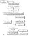
- FIG. 1depicts a flow diagram illustrating a first embodiment of the process for germanium growth on silicon in accordance with the present invention.
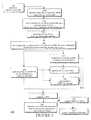
- FIG. 2depicts a flow diagram illustrating a second embodiment of the process for poly-Ge growth on silicon in accordance with the present invention.
- step 110the manufacturing of a chip employs a standard CMOS flow with a silicon substrate.
- the process 100continues until the highest temperature step, typically the salicide annealing, is performed.
- step 120the process 100 deposits a first silicon oxynitride layer.
- Step 120is typically a conventional CMOS process step.
- One of ordinary skill in the artshould recognize that the deposition of one or more silicon oxynitride layers is typical in a CMOS process. Similar or various types of compositions of silicon oxynitride can be practiced without departing from the spirit of the present invention.
- the first oxynitride layeris then patterned in order to expose areas of the underlying Si substrate in the process step 130 .
- One embodiment illustrating the present inventionincludes depositing the silicon oxynitride layer by selecting a suitable SON film in which the oxygen and nitrogen content are both allowed to vary in the full composition range including stoichiometric SiO2 and Si3N4.
- the scope of the present inventionextends to choosing the dielectric film with properties such that the germanium will not grow on the film.
- the dielectric filmcould be selected to have properties where the germanium would grow on top of the film, allowing a subsequent etch to define the shape of the deposited germanium.
- One of ordinary skill in the artshould recognize that variations in the present material systems, as well as new material systems that carry the properties as described above, such as low-k dielectrics, can be practiced without departing from the spirit of the present invention.
- germanium growth in a standard CMOS process in the first embodimentis intended as an example.
- One of ordinary skill in the artshould recognize that the present invention can be extended or modified to incorporate germanium growth in BICMOS, SOI, SiGe BICMOS, SOS, and other similar manufacturing processes.
- a windowis opened in the first silicon oxynitride layer exposing the active silicon (Si) layer.
- the shape of the openingdepends on photonic and material factors.
- the active windows crated in step 130have rectangular shapes with sides oriented along the ⁇ 011> silicon crystallographic direction. Windows oriented in other crystalline directions could also be fabricated.
- the feedback on the optimal shape of the active Si layeris provided by the morphological and structural characteristics of the Ge deposited on the active Si layer.
- the process 100performs an epi-clean step 140 on the silicon oxynitride patterned substrate formed in step 130 . After a layer removal of the silicon oxynitride layer, an epi-like active silicon surface is recovered. In this procedure, an ex-situ wet chemical cleaning based on hydrofluoric acid (HF) solution is followed by an in-situ annealing in dihydrogen/DCS atmosphere.
- the substrate temperatureis approximately 700° C.
- Windows in to the SON layer formed during step 120 and 130are designed as test structures in order to perform a direct morphological inspection by means of Scanning Probe Microscopy on test wafers which have been pulled out from the process after the step 140 .
- Pyramidal-shaped defectsare expected to be formed by Si—O and Si—C surface contamination.
- Substrate cleanlinesscan be evaluated also by growing a Si buffer layer by silane CVD and evaluating the pit defect density and morphology. These defects are formed at the substrate-epilayer interface, and provides a marker of the substrate surface quality.
- the compatibility of the high temperature step relative to the entire fabrication processshould be verified.
- the implanted doping distribution and the effect of the thermal stress on the existing structuresare monitored.
- a thin Ge layeris deposited at a low temperature for strain relaxation in the lattice mismatched Ge/Si heterostructure.
- a temperature as low as 370° C. and a deposition rate of the order of 3-5 nm/minare typical values for this growth step using germane on clean silicon.
- Growth dynamicsis characterized and optimized in this step.
- An objectiveis to optimize the kinetics/thermodynamics of the germane chemisorption at the Si surface.
- the parameters that may varyinclude: total reaction-gas pressure, partial pressure of the Ge in the H carrier gas, substrate temperature, and amount of deposited material.
- the optimization feedbackis provided by investigating the structural, morphological, and electrical properties of the deposited material. Other factors are also evaluated in this step including the growth rate, the incubation time, the defect density, and the stress relaxation via misfit dislocation insertion and/or surface roughening. These quantities are correlated with the shape and size of the opening in the first silicon oxynitride layer formed in step 130 where the material has to be deposited in step 150 and 160 .
- One objective in step 150is to find the optimal thickness for the stress relaxation with the lowest density of point defects with a smooth surface.
- a Ge layer thickness in the 30 to 70 nm rangeis typical AFM/SEM measurement, a ⁇ -Raman measurement, and an XTEM measurement are performed in order to investigate the morphological and structural properties of the Ge deposited film. Measurements are conducted on window openings of the silicon oxynitride windows formed in step 130 which have a size and shape suitable for an optoelectronics application. In larger windows which can be used for metrology purposes, the growth selectivity is also investigated using a process such as spatially resolved SIMS—Secondary Ion Mass Spectroscopy. Devices are designed to test the compatibility of this process step with the entire production flow.
- step 160there is a high temperature deposition of a Ge (HTGE—high temperature Ge) active layer, which serves as the core of an active region.
- HTGEhigh temperature Ge
- the Ge growthproceeds in a quasi-homoepitaxial manner.
- the high temperature of the depositionpromotes the growth in a layer-by-layer mode, leading to both a desirable crystal quality and a smooth film surface.
- the higher temperaturealso changes the surface reaction, allowing an increased growth rate.
- Typical values for this stepare deposition temperatures between 600-700° C. and a growth rate of 10-20 nm/min.
- the deposited film thicknessis dependent on the device design: 300 nm can be a guidelines.
- This designtakes into account the upper limit of Ge thickness due to the layer thickness of the dielectric stack subsequently deposited, and the length of the contacts that penetrate the dielectric layer immediately placed over the germanium.
- the optimal combination of growth parametersis also influenced by their impact on the film homogeneity over the substrate.
- the optimal growth parametersresult in a quasi-fully relaxed, epitaxial, mono-crystalline, smooth planar Ge active layer with a low point defect and threading dislocation density.
- test structures/test measurementssimilar to the previous step, an AFM/SEM measurement, a ⁇ -Raman measurement, and an XTEM measurement are taken. These measurements are performed on a window opening on the silicon oxynitride layer formed in step 130 which have a size and shape suitable for an optoelectronics application.
- XRDin comparison with ⁇ -Raman measurement provides insight on the crystalline quality and the residual stress. Growth selectivity at this higher deposition temperature is monitored in conjunction with the material homogeneity over the wafer on a structure suitable for metrology measurements. Hall Effect measurements may yield information on carrier mobility.
- the Ge filmis implanted to fabricate the type of device that is desired.
- the process 100performs the Ge doping in order to obtain the energy band profile requested by the device design.
- the annealing treatment for the implant activationis performed in RTA (Rapid Thermal Annealing) conditions: typical substrate temperature in the step will be in the 450-600° C. range.
- RTARapid Thermal Annealing
- the step 170 of implantationcan be repeated with different doses, energies, and species if needed in the final device design.
- test structures/test measurementsSIMS and spreading resistance measurements are used to study the dopant spatial distribution and their electrical activity in the high temperature Ge active layer.
- integrated test-deviceswill be fabricated: dopant diffusion, and Ge—Ge leakage current being the main concerns.
- step 180the process 100 deposits a second silicon oxynitride layer for Ge surface passivation.
- the deposition of a second silicon oxynitride layeris completed in this step.
- the second silicon oxynitride layeris a suitable material for Ge surface passivation.
- This same silicon oxynitride layer, or an additional one with the same of different composition, layermay also be used to stop the via etch on top of the Ge layer.
- Steps 161 , 162 , and 163are optional steps for an alternative process.
- the surface qualitycan be improved by depositing Antimony (Sb) during the growth.
- SbAntimony
- the surfactant action of this elementreduces the roughening/islanding phenomenon similar to Hydrogen.
- the use of Sb as a surfactantallows the deposition of a thinner Ge buffer layer in step 150 , and increases the average growth rate of the process as the deposition temperature can be kept higher.
- This process stepoperates as an alternate solution to the deposition of the high temperature Ge active layer in step 160 .
- the test structures/test measurementsare the same as those requested in step 160 .
- a cautionary measureis taken in the event that unintentional n-doping is generated from the Sb.
- Step 162quenches the defects in the Ge films. Threading dislocations are common defects in Ge films grown by using this technique, and their density depends on the quality of the Ge/Si heterointerface. Quenching is performed by means of a post-annealing process wherein the substrate temperature is modulated between a low temperature and a high temperature for an optimal number of cycles. Typical values are 700° and 900° C. as minimum and maximum temperature values in a 10 cycle repetition. A forming (inert) gas can be used to prevent surface contamination during the treatment. It is noted that such a high temperature process can enhance GeSi intermixing at the interface. This intermixing actually helps the stress relaxation, offering an alternate way to perform strain reduction (strain buffering). The shape of the active window is designed to promote dislocation mobility and quenching. This process has been demonstrated to be effective on Ge layer deposited on bare (non-patterned) Si substrate.
- an epi-smooth processis performed on the high temperature Ge active layer deposited in step 160 .
- the strain relaxation process in the high temperature Ge active layercan, depending on the kinetics, induce surface roughening (for example, RMS roughness of the order of 10 nm).
- the surface planarity requested by the subsequent process flowcan be recovered by means of an epi-smoothing process.
- the surface of the high temperature active Ge active layeris exposed to a gas mixture made of germane, hydrogen, and hydrogen chloride at a surface temperature in the 600-700° C. range.
- the ridges of the rough surfaceare smoothed by this process because the etch rate is dependent on the local strain conditions of the surface.
- this process stepis performed immediately after the high temperature Ge active deposition and the test structure/measurement is the same as in step 160 .
- the objective of this optimization processis to obtain a smoother surface that can meet the specification of the subsequent process in the standard CMOS flow: a roughness RMS of 1 nm or less can be considered typical.
- a dielectric stackis deposited over the second oxynitride layer formed in step 180 .
- the process 100then returns to the standard CMOS process flow 195 .
- FIG. 2therein is shown a flow diagram illustrating a second embodiment of a process for poly-Ge growth.
- the manufacturing of a chipemploys a standard CMOS flow with a silicon substrate using a silicon-on-insulator process.
- the process 200continues until the salicide annealing.
- the process 200deposits a first silicon oxynitride layer. This oxynitride layer is then patterned in order to expose areas of the underlying Si substrate in the process step 230 .
- the process 200opens a window in the first silicon oxynitride layer onto the active silicon layer. This step defines the opening to the active Si substrate.
- the substratecan be n-doped.
- the active window shape created in step 230is optimized considering photonic design requirements.
- a standard, ex-situ wet etching/cleaning stepis performed prior to sample loading in the reactor where the subsequent process step will take place.
- An in-situ high-temperature stepis optional.
- the process 200deposits a seed layer in step 240 , made of either Ge or Si.
- the saturation of the Si bonds by contaminants (native oxide etc.)leads to a poor sticking of the germane molecules to the surface.
- a first Ge layercan be deposited, exploiting the physisorption mechanism to act as a seed layer for the subsequent growth.
- One way to obtain physiororption in a typical CVD process reactoris, for example, the following: the molecules containing the atom are cracked and deposited (e.g. germane molecule to obtain germanium) by temperature pulsing or hot wire catalysis, away from the substrate surface.
- the resulting Ge layeris either poly-crystalline or amorphous.
- An in-situ-deposited poly-Si layercould also play the role of seed for the subsequent growth by providing high density of dangling bonds.
- step 250the process 200 deposits a poly-crystalline germanium active layer on the seed deposited in step 240 .
- the size of the poly-crystalliteis optimized by tuning the growth rate and the deposition temperature: 350-500° C. are typical values for this step.
- the size of the poly-crystalliteis related to the strain energy stored in the grain itself and, thus, to its optical properties.
- the influence of the film thickness on the grain size and shapeis optimized in order to increase the device collection length.
- the poly-Ge layer thicknessis also dependent on the device design.
- the deposition parametersalso influence the H:Ge bonds at the grain boundaries, i.e. the is surface electronic states, and thus the electrical properties of the film.
- the eventual poly-Ge layer thicknessis dependent on the device design. Therefore, the film morphology and structure, such as the grain size and orientation, affect the material electrical properties which need to be considered to optimize a device design.
- AFM/SEM measurement, ⁇ -Raman measurement, and XTEM measurementprovide insights on surface morphology, crystalline quality, and residual strain status.
- Metrology measurementsprovides information on growth rate and material homogeneity. These measurements are performed on and off the window openings in step 230 , i.e. on the film deposited on the Si substrate or on the silicon oxynitride mask respectively.
- the poly-crystalline growthis not selective and a Ge-pad definition step is typically added.
- a Chlorine-based (Cl-based) etchcan be used in order to remove the Ge deposited outside the openings of windows in the first silicon oxynitride layer.
- an in-situ etch using an HCl-hydrogen mixturecould be used. Metrology and surface analysis measurement is used to confirm a complete removal of unwanted material. If poly-Si has been used as the seed layer, it will be removed by this process step.
- test structures/test measurementsmaterial homogeneity is monitored on a structure suitable for metrology measurements both over the wafer and on a window opening site formed in step 230 .
- Hall Effect measurementsprovide insight on carrier mobility and on the electrical properties of the deposited film.
- a spreading resistance testis also useful.
- Geis doped or implanted in order to obtain the energy band profile requested by the device design (dopant compensation).
- a post annealing treatmentis performed in RTA conditions at a substrate temperature in the 450-600° C. range.
- SIMS, and spreading resistance measurementsare used to study the dopant spatial distribution and their electrical activity in the Ge pad layer.
- a suitable deviceis designed for testing the impact of this step on the process flow (dopant diffusion, Ge—Ge leakage are examples).
- the process 200deposits a second silicon oxynitride layer for Ge surface passivation.
- the silicon oxynitrideis a suitable material for Ge surface passivation.
- the silicon oxynitride layeris also needed to stop the via etch on top of the Ge layer.
- the process 200returns to standard CMOS process flow.
- Steps 251 , 255 , and 256are optional steps in an alternate process.
- a low temperature variation of the technique described in step 250is performed, referred to hereinafter as “age active”.
- the deposition temperatureis kept as low as 300° C., while growth rate can be kept high by modifying the growth parameters.
- the depositionresults in an amorphous Ge layer with high H content.
- test structures/test measurementsthe same procedures are used as those in step 250 .
- step 255long anneal (for example, a few hours) and low-temperature (300-350° C.) treatments are performed on the amorphous germanium active deposited layer in a controlled atmosphere. This treatment releases the hydrogen stored in the material is during the growth performed in steps 250 and 251 , and it provides short range ordering in the amorphous film formed in step 251 , leading to the formation of poly-crystallite sites that acts as centers for re-crystallization in step 255 .
- a short annealing(for example, can be RTA or pulsed) is performed on the amorphous or poly-crystalline film obtained in steps 250 , 251 , and 255 .
- This annealingis done at a high temperature (450-550° C.) and in a controlled atmosphere (for example, gas mixture composition).
- This treatmentresults in the formation of large Ge poly-crystalline grains.
- test structures/test measurementsthe same procedures are used as those in step 250 .
Landscapes
- Recrystallisation Techniques (AREA)
- Insulated Gate Type Field-Effect Transistor (AREA)
- Metal-Oxide And Bipolar Metal-Oxide Semiconductor Integrated Circuits (AREA)
- Electrodes Of Semiconductors (AREA)
Abstract
Description
- This application claims priority from U.S. Provisional Application Ser. No. 60/389,962, filed on Jun. 19, 2002, U.S. Provisional Application Ser. No. 60/391,277, filed on Jun. 24, 2002, U.S. Provisional Application Ser. No. 60/393,484, filed on Jul. 3, 2002, U.S. Provisional Application Ser. No. 60/432,946, filed on Dec. 12, 2002, U.S. Provisional Application Ser. No. 60/432,925, filed on Dec. 12, 2002, and U.S. Provisional Application Ser. No. 60/433,470, filed on Dec. 13, 2002.[0001]
- 1. Field of the Invention[0002]
- The invention relates generally to the field of chip manufacturing process, and is more particularly to fabrication with one or more germanium layers.[0003]
- 2. Description of Related Art[0004]
- The convergence of silicon and optical fabrication processes presents an attractive manufacturing solution by leveraging the use of a standard CMOS (complementary metal-oxide semiconductor) manufacturing process. Some optical companies have selected III-V semiconductors to provide high detection efficiency, but this selection poses difficult challenges in incorporating a III-V material in a standard CMOS technology. For additional background information on SiGe structures, the reader is referred to “Metal-semiconductor-metal near-infrared light detector based on epitaxial Ge/Si”, by L. Colace et al. and G. Capellini et al., Applied Physics Letters, Vol. 72, No. 24, pp. 3175-3177.[0005]
- Accordingly, it is desirable to incorporate optical telecommunication systems within a standard CMOS process.[0006]
- The invention discloses processes for deposition of one or more Germanium (Ge) layers during a standard CMOS process on a monolithic device. The insertion of one or more Ge layers enables light to be easily converted into electrical signals. Standard metals can be attached directly to the Ge in completing an electrical circuit. Vias can also be used to connect to a Ge layer.[0007]
- In a first aspect of the invention, a method is described for incorporating the deposition of Ge at multiple temperatures in a standard CMOS process. A silicon oxynitride (SON) layer is used as a mask for selective Ge growth on the Si area left uncovered by the SON patterning. A thin Ge layer is then deposited from a germane Chemical-Vapor Deposition (CVD) carried out at a temperature below, for example, a temperature of 370° C. can be used if the reacting gas contains germane. Below this temperature, the Hydrogen (H) contained in the process gas may saturate the dangling bonds of the growing surface, thereby modifying the surface energy. The surfactant is action of the Hydrogen hinders the islanding phenomenon (Stranski-Krastanov growth) in the Germanium/Silicon (Ge/Si) heterostructure. It also relaxes the strain forcing the misfit dislocation insertion at the heterojunction, thus providing a seed for the nucleation of a strain-relaxed Ge film. The growth of this layer wick occurs only on the opening in the SON mask because the germane-deposition catalysis on the SON surface is not effective. After the strain is relaxed in the Ge film, a thicker Ge layer is deposited at a higher deposition temperature (for example, greater than 600° C.) in order to have, for example a layer-by-layer growth mode. The higher temperature also allows an increase in the growth rate. In order to reduce the defect density, a post-growth annealing process may be performed. The film undergoes a thermal cycling treatment typically between about 700° C. and 900° C. The film thus obtained is mono-crystalline, epitaxial, and has a small surface roughness (about[0008]1 nm RMS roughness expected).
- In a second aspect of the invention, a method is disclosed for incorporating the deposition of poly-Ge growth into a standard CMOS process. In this aspect, a low temperature (for example, T<500° C.) poly-Ge film is deposited on a Si active area. This deposition is catalyzed by a seed layer made of either poly/amorphous-Si or amorphous-Ge. Due to the electronic surface states on the crystallite boundaries, the film is “unintentionally p-doped” typically in the 10[0009]18cm−3range: the Fermi level is in fact pinned close to the top of the Ge valence band.
- Advantageously, with the insertion of one or more Ge layers, the present invention provides the capability of converting an optical signal carried at a wavelength range that can be absorbed by the germanium into an electrical signal.[0010]
- Other structures and methods are disclosed in the detailed description below. This summary does not purport to define the invention. The invention is defined by the claims.[0011]
- FIG. 1 depicts a flow diagram illustrating a first embodiment of the process for germanium growth on silicon in accordance with the present invention.[0012]
- FIG. 2 depicts a flow diagram illustrating a second embodiment of the process for poly-Ge growth on silicon in accordance with the present invention.[0013]
- Referring now to FIG. 1, therein is shown a flow diagram illustrating a first embodiment of the[0014]
process 100 for incorporating germanium growth in a standard CMOS process. Instep 110, the manufacturing of a chip employs a standard CMOS flow with a silicon substrate. Theprocess 100 continues until the highest temperature step, typically the salicide annealing, is performed. In step120, theprocess 100 deposits a first silicon oxynitride layer. Step120 is typically a conventional CMOS process step. One of ordinary skill in the art should recognize that the deposition of one or more silicon oxynitride layers is typical in a CMOS process. Similar or various types of compositions of silicon oxynitride can be practiced without departing from the spirit of the present invention. The first oxynitride layer is then patterned in order to expose areas of the underlying Si substrate in theprocess step 130. One embodiment illustrating the present invention includes depositing the silicon oxynitride layer by selecting a suitable SON film in which the oxygen and nitrogen content are both allowed to vary in the full composition range including stoichiometric SiO2 and Si3N4. The scope of the present invention extends to choosing the dielectric film with properties such that the germanium will not grow on the film. Alternatively, the dielectric film could be selected to have properties where the germanium would grow on top of the film, allowing a subsequent etch to define the shape of the deposited germanium. One of ordinary skill in the art should recognize that variations in the present material systems, as well as new material systems that carry the properties as described above, such as low-k dielectrics, can be practiced without departing from the spirit of the present invention. - The incorporation of germanium growth in a standard CMOS process in the first embodiment is intended as an example. One of ordinary skill in the art should recognize that the present invention can be extended or modified to incorporate germanium growth in BICMOS, SOI, SiGe BICMOS, SOS, and other similar manufacturing processes.[0015]
- At[0016]
step 130, a window is opened in the first silicon oxynitride layer exposing the active silicon (Si) layer. The shape of the opening depends on photonic and material factors. The active windows crated instep 130 have rectangular shapes with sides oriented along the <011> silicon crystallographic direction. Windows oriented in other crystalline directions could also be fabricated. The feedback on the optimal shape of the active Si layer is provided by the morphological and structural characteristics of the Ge deposited on the active Si layer. - The[0017]
process 100 performs an epi-clean step 140 on the silicon oxynitride patterned substrate formed instep 130. After a layer removal of the silicon oxynitride layer, an epi-like active silicon surface is recovered. In this procedure, an ex-situ wet chemical cleaning based on hydrofluoric acid (HF) solution is followed by an in-situ annealing in dihydrogen/DCS atmosphere. The substrate temperature is approximately 700° C. - Windows in to the SON layer formed during[0018]
step 120 and130 are designed as test structures in order to perform a direct morphological inspection by means of Scanning Probe Microscopy on test wafers which have been pulled out from the process after thestep 140. Pyramidal-shaped defects are expected to be formed by Si—O and Si—C surface contamination. Substrate cleanliness can be evaluated also by growing a Si buffer layer by silane CVD and evaluating the pit defect density and morphology. These defects are formed at the substrate-epilayer interface, and provides a marker of the substrate surface quality. The compatibility of the high temperature step relative to the entire fabrication process should be verified. The implanted doping distribution and the effect of the thermal stress on the existing structures are monitored. - At[0019]
step 150, a thin Ge layer is deposited at a low temperature for strain relaxation in the lattice mismatched Ge/Si heterostructure. A temperature as low as 370° C. and a deposition rate of the order of 3-5 nm/min are typical values for this growth step using germane on clean silicon. - Growth dynamics is characterized and optimized in this step. An objective is to optimize the kinetics/thermodynamics of the germane chemisorption at the Si surface. The parameters that may vary include: total reaction-gas pressure, partial pressure of the Ge in the H carrier gas, substrate temperature, and amount of deposited material. The optimization feedback is provided by investigating the structural, morphological, and electrical properties of the deposited material. Other factors are also evaluated in this step including the growth rate, the incubation time, the defect density, and the stress relaxation via misfit dislocation insertion and/or surface roughening. These quantities are correlated with the shape and size of the opening in the first silicon oxynitride layer formed in[0020]
step 130 where the material has to be deposited instep step 150 is to find the optimal thickness for the stress relaxation with the lowest density of point defects with a smooth surface. A Ge layer thickness in the 30 to 70 nm range is typical AFM/SEM measurement, a μ-Raman measurement, and an XTEM measurement are performed in order to investigate the morphological and structural properties of the Ge deposited film. Measurements are conducted on window openings of the silicon oxynitride windows formed instep 130 which have a size and shape suitable for an optoelectronics application. In larger windows which can be used for metrology purposes, the growth selectivity is also investigated using a process such as spatially resolved SIMS—Secondary Ion Mass Spectroscopy. Devices are designed to test the compatibility of this process step with the entire production flow. - At[0021]
step 160, there is a high temperature deposition of a Ge (HTGE—high temperature Ge) active layer, which serves as the core of an active region. After the heterostructure stress relaxation instep 150, the Ge growth proceeds in a quasi-homoepitaxial manner. The high temperature of the deposition promotes the growth in a layer-by-layer mode, leading to both a desirable crystal quality and a smooth film surface. The higher temperature also changes the surface reaction, allowing an increased growth rate. Typical values for this step are deposition temperatures between 600-700° C. and a growth rate of 10-20 nm/min. The deposited film thickness is dependent on the device design: 300 nm can be a guidelines. This design takes into account the upper limit of Ge thickness due to the layer thickness of the dielectric stack subsequently deposited, and the length of the contacts that penetrate the dielectric layer immediately placed over the germanium. The optimal combination of growth parameters (material deposited, gas flows, partial pressures, and deposition temperature) is also influenced by their impact on the film homogeneity over the substrate. The optimal growth parameters result in a quasi-fully relaxed, epitaxial, mono-crystalline, smooth planar Ge active layer with a low point defect and threading dislocation density. - On the test structures/test measurements, similar to the previous step, an AFM/SEM measurement, a μ-Raman measurement, and an XTEM measurement are taken. These measurements are performed on a window opening on the silicon oxynitride layer formed in[0022]
step 130 which have a size and shape suitable for an optoelectronics application. In larger windows which can be used for metrology purpose, XRD in comparison with μ-Raman measurement provides insight on the crystalline quality and the residual stress. Growth selectivity at this higher deposition temperature is monitored in conjunction with the material homogeneity over the wafer on a structure suitable for metrology measurements. Hall Effect measurements may yield information on carrier mobility. - At[0023]
step 170, the Ge film is implanted to fabricate the type of device that is desired. In this step, theprocess 100 performs the Ge doping in order to obtain the energy band profile requested by the device design. The annealing treatment for the implant activation is performed in RTA (Rapid Thermal Annealing) conditions: typical substrate temperature in the step will be in the 450-600° C. range. Thestep 170 of implantation can be repeated with different doses, energies, and species if needed in the final device design. - As for test structures/test measurements: SIMS and spreading resistance measurements are used to study the dopant spatial distribution and their electrical activity in the high temperature Ge active layer. In order to test the impact of this step on the process flow integrated test-devices will be fabricated: dopant diffusion, and Ge—Ge leakage current being the main concerns.[0024]
- In[0025]
step 180, theprocess 100 deposits a second silicon oxynitride layer for Ge surface passivation. The deposition of a second silicon oxynitride layer is completed in this step. The second silicon oxynitride layer is a suitable material for Ge surface passivation. This same silicon oxynitride layer, or an additional one with the same of different composition, layer may also be used to stop the via etch on top of the Ge layer. - [0026]
Steps step 161, the surface quality can be improved by depositing Antimony (Sb) during the growth. The surfactant action of this element reduces the roughening/islanding phenomenon similar to Hydrogen. The use of Sb as a surfactant allows the deposition of a thinner Ge buffer layer instep 150, and increases the average growth rate of the process as the deposition temperature can be kept higher. This process step operates as an alternate solution to the deposition of the high temperature Ge active layer instep 160. The test structures/test measurements are the same as those requested instep 160. A cautionary measure is taken in the event that unintentional n-doping is generated from the Sb. - [0027]
Step 162 quenches the defects in the Ge films. Threading dislocations are common defects in Ge films grown by using this technique, and their density depends on the quality of the Ge/Si heterointerface. Quenching is performed by means of a post-annealing process wherein the substrate temperature is modulated between a low temperature and a high temperature for an optimal number of cycles. Typical values are 700° and 900° C. as minimum and maximum temperature values in a 10 cycle repetition. A forming (inert) gas can be used to prevent surface contamination during the treatment. It is noted that such a high temperature process can enhance GeSi intermixing at the interface. This intermixing actually helps the stress relaxation, offering an alternate way to perform strain reduction (strain buffering). The shape of the active window is designed to promote dislocation mobility and quenching. This process has been demonstrated to be effective on Ge layer deposited on bare (non-patterned) Si substrate. - On test structures/test measurements, the film is investigated by both XTEM-TEM (Transmission Electron Microscopy) and etch pit counting in order to obtain the threading dislocation density. SIMS characterization of the interface is needed in order to investigate the extent of the Ge—Si intermixing. The compatibility of this process step (dopant diffusion) with the whole flow is tested by means of suitable devices.[0028]
- At[0029]
step 163, an epi-smooth process is performed on the high temperature Ge active layer deposited instep 160. The strain relaxation process in the high temperature Ge active layer can, depending on the kinetics, induce surface roughening (for example, RMS roughness of the order of 10 nm). The surface planarity requested by the subsequent process flow can be recovered by means of an epi-smoothing process. In this step, the surface of the high temperature active Ge active layer is exposed to a gas mixture made of germane, hydrogen, and hydrogen chloride at a surface temperature in the 600-700° C. range. The ridges of the rough surface are smoothed by this process because the etch rate is dependent on the local strain conditions of the surface. On test structures/test measurements, this process step is performed immediately after the high temperature Ge active deposition and the test structure/measurement is the same as instep 160. The objective of this optimization process is to obtain a smoother surface that can meet the specification of the subsequent process in the standard CMOS flow: a roughness RMS of 1 nm or less can be considered typical. - At[0030]
step 190, a dielectric stack is deposited over the second oxynitride layer formed instep 180. Theprocess 100 then returns to the standardCMOS process flow 195. - In FIG. 2, therein is shown a flow diagram illustrating a second embodiment of a process for poly-Ge growth. At[0031]
step 210, the manufacturing of a chip employs a standard CMOS flow with a silicon substrate using a silicon-on-insulator process. Theprocess 200 continues until the salicide annealing. Instep 220, theprocess 200 deposits a first silicon oxynitride layer. This oxynitride layer is then patterned in order to expose areas of the underlying Si substrate in theprocess step 230. - At[0032]
step 230, theprocess 200 opens a window in the first silicon oxynitride layer onto the active silicon layer. This step defines the opening to the active Si substrate. The substrate can be n-doped. The active window shape created instep 230 is optimized considering photonic design requirements. A standard, ex-situ wet etching/cleaning step is performed prior to sample loading in the reactor where the subsequent process step will take place. An in-situ high-temperature step is optional. - The[0033]
process 200 deposits a seed layer instep 240, made of either Ge or Si. The saturation of the Si bonds by contaminants (native oxide etc.) leads to a poor sticking of the germane molecules to the surface. To remedy this, a first Ge layer can be deposited, exploiting the physisorption mechanism to act as a seed layer for the subsequent growth. One way to obtain physiororption in a typical CVD process reactor, is, for example, the following: the molecules containing the atom are cracked and deposited (e.g. germane molecule to obtain germanium) by temperature pulsing or hot wire catalysis, away from the substrate surface. Depending on the kinetics/thermodynamics condition of the seed layer deposition, the resulting Ge layer is either poly-crystalline or amorphous. An in-situ-deposited poly-Si layer could also play the role of seed for the subsequent growth by providing high density of dangling bonds. - In[0034]
step 250 theprocess 200 deposits a poly-crystalline germanium active layer on the seed deposited instep 240. Once the seed layer has been deposited, the size of the poly-crystallite is optimized by tuning the growth rate and the deposition temperature: 350-500° C. are typical values for this step. The size of the poly-crystallite is related to the strain energy stored in the grain itself and, thus, to its optical properties. The influence of the film thickness on the grain size and shape is optimized in order to increase the device collection length. The poly-Ge layer thickness is also dependent on the device design. The deposition parameters also influence the H:Ge bonds at the grain boundaries, i.e. the is surface electronic states, and thus the electrical properties of the film. The eventual poly-Ge layer thickness is dependent on the device design. Therefore, the film morphology and structure, such as the grain size and orientation, affect the material electrical properties which need to be considered to optimize a device design. - On test structures/test measurements, AFM/SEM measurement, μ-Raman measurement, and XTEM measurement provide insights on surface morphology, crystalline quality, and residual strain status. Metrology measurements provides information on growth rate and material homogeneity. These measurements are performed on and off the window openings in[0035]
step 230, i.e. on the film deposited on the Si substrate or on the silicon oxynitride mask respectively. - At[0036]
step 260, the poly-crystalline growth is not selective and a Ge-pad definition step is typically added. A Chlorine-based (Cl-based) etch can be used in order to remove the Ge deposited outside the openings of windows in the first silicon oxynitride layer. Alternatively, an in-situ etch using an HCl-hydrogen mixture could be used. Metrology and surface analysis measurement is used to confirm a complete removal of unwanted material. If poly-Si has been used as the seed layer, it will be removed by this process step. - As for test structures/test measurements, material homogeneity is monitored on a structure suitable for metrology measurements both over the wafer and on a window opening site formed in[0037]
step 230. Hall Effect measurements provide insight on carrier mobility and on the electrical properties of the deposited film. A spreading resistance test is also useful. - At[0038]
step 270, Ge is doped or implanted in order to obtain the energy band profile requested by the device design (dopant compensation). A post annealing treatment is performed in RTA conditions at a substrate temperature in the 450-600° C. range. On test structures/test measurements, SIMS, and spreading resistance measurements are used to study the dopant spatial distribution and their electrical activity in the Ge pad layer. A suitable device is designed for testing the impact of this step on the process flow (dopant diffusion, Ge—Ge leakage are examples). - At[0039]
step 280, theprocess 200 deposits a second silicon oxynitride layer for Ge surface passivation. The silicon oxynitride is a suitable material for Ge surface passivation. The silicon oxynitride layer is also needed to stop the via etch on top of the Ge layer. Atstep 290, theprocess 200 returns to standard CMOS process flow. - [0040]
Steps step 251, a low temperature variation of the technique described instep 250 is performed, referred to hereinafter as “age active”. After the deposition of a Ge or Si seed layer, the deposition temperature is kept as low as 300° C., while growth rate can be kept high by modifying the growth parameters. The deposition results in an amorphous Ge layer with high H content. Regarding test structures/test measurements, the same procedures are used as those instep 250. - At[0041]
step 255, long anneal (for example, a few hours) and low-temperature (300-350° C.) treatments are performed on the amorphous germanium active deposited layer in a controlled atmosphere. This treatment releases the hydrogen stored in the material is during the growth performed insteps step 251, leading to the formation of poly-crystallite sites that acts as centers for re-crystallization instep 255. - At[0042]
step 256, a short annealing (for example, can be RTA or pulsed) is performed on the amorphous or poly-crystalline film obtained insteps step 250. - The above embodiments are only illustrative of the principles of this invention and are not intended to limit the invention to the particular embodiments described. Accordingly, various modifications, adaptations, and combinations of various features of the described embodiments can be practiced without departing from the scope of the invention as set forth in the appended claims.[0043]
Claims (173)
Priority Applications (4)
| Application Number | Priority Date | Filing Date | Title |
|---|---|---|---|
| US10/458,165US6887773B2 (en) | 2002-06-19 | 2003-06-10 | Methods of incorporating germanium within CMOS process |
| EP04718583.0AEP1631980B1 (en) | 2003-06-10 | 2004-03-08 | Methods of incorporating germanium within cmos process |
| PCT/US2004/007126WO2005006406A2 (en) | 2003-06-10 | 2004-03-08 | Methods of incorporating germanium within cmos process |
| US11/064,035US7262117B1 (en) | 2003-06-10 | 2005-02-22 | Germanium integrated CMOS wafer and method for manufacturing the same |
Applications Claiming Priority (7)
| Application Number | Priority Date | Filing Date | Title |
|---|---|---|---|
| US38996202P | 2002-06-19 | 2002-06-19 | |
| US39127702P | 2002-06-24 | 2002-06-24 | |
| US39348402P | 2002-07-03 | 2002-07-03 | |
| US43292502P | 2002-12-12 | 2002-12-12 | |
| US43294602P | 2002-12-12 | 2002-12-12 | |
| US43347002P | 2002-12-13 | 2002-12-13 | |
| US10/458,165US6887773B2 (en) | 2002-06-19 | 2003-06-10 | Methods of incorporating germanium within CMOS process |
Related Child Applications (1)
| Application Number | Title | Priority Date | Filing Date |
|---|---|---|---|
| US11/064,035Continuation-In-PartUS7262117B1 (en) | 2003-06-10 | 2005-02-22 | Germanium integrated CMOS wafer and method for manufacturing the same |
Publications (2)
| Publication Number | Publication Date |
|---|---|
| US20040092104A1true US20040092104A1 (en) | 2004-05-13 |
| US6887773B2 US6887773B2 (en) | 2005-05-03 |
Family
ID=34061872
Family Applications (1)
| Application Number | Title | Priority Date | Filing Date |
|---|---|---|---|
| US10/458,165Expired - LifetimeUS6887773B2 (en) | 2002-06-19 | 2003-06-10 | Methods of incorporating germanium within CMOS process |
Country Status (3)
| Country | Link |
|---|---|
| US (1) | US6887773B2 (en) |
| EP (1) | EP1631980B1 (en) |
| WO (1) | WO2005006406A2 (en) |
Cited By (45)
| Publication number | Priority date | Publication date | Assignee | Title |
|---|---|---|---|---|
| US20070065921A1 (en)* | 2000-09-12 | 2007-03-22 | Massachusetts Institute Of Technology | Methods and products related to producing low molecular weight heparin |
| US20070075264A1 (en)* | 2005-09-30 | 2007-04-05 | Virgin Islands Microsystems, Inc. | Electron beam induced resonance |
| US20070190794A1 (en)* | 2006-02-10 | 2007-08-16 | Virgin Islands Microsystems, Inc. | Conductive polymers for the electroplating |
| US20070200646A1 (en)* | 2006-02-28 | 2007-08-30 | Virgin Island Microsystems, Inc. | Method for coupling out of a magnetic device |
| US20070252089A1 (en)* | 2006-04-26 | 2007-11-01 | Virgin Islands Microsystems, Inc. | Charged particle acceleration apparatus and method |
| US20070257749A1 (en)* | 2006-05-05 | 2007-11-08 | Virgin Islands Microsystems, Inc. | Coupling a signal through a window |
| US20070257738A1 (en)* | 2006-05-05 | 2007-11-08 | Virgin Islands Microsystems, Inc. | Top metal layer shield for ultra-small resonant structures |
| US20070258690A1 (en)* | 2006-05-05 | 2007-11-08 | Virgin Islands Microsystems, Inc. | Integration of electromagnetic detector on integrated chip |
| US20070257199A1 (en)* | 2006-05-05 | 2007-11-08 | Virgin Islands Microsystems, Inc. | Heterodyne receiver using resonant structures |
| US20080017101A1 (en)* | 2004-02-27 | 2008-01-24 | Asm America, Inc. | Germanium Deposition |
| US20080073590A1 (en)* | 2006-09-22 | 2008-03-27 | Virgin Islands Microsystems, Inc. | Free electron oscillator |
| US7361574B1 (en)* | 2006-11-17 | 2008-04-22 | Sharp Laboratories Of America, Inc | Single-crystal silicon-on-glass from film transfer |
| EP1631980A4 (en)* | 2003-06-10 | 2008-10-01 | Luxtera Inc | METHOD FOR INTEGRATING GERMANIUM FROM CMOS PROCESSES |
| US7558490B2 (en) | 2006-04-10 | 2009-07-07 | Virgin Islands Microsystems, Inc. | Resonant detector for optical signals |
| US7557365B2 (en) | 2005-09-30 | 2009-07-07 | Virgin Islands Microsystems, Inc. | Structures and methods for coupling energy from an electromagnetic wave |
| US7569836B2 (en) | 2006-05-05 | 2009-08-04 | Virgin Islands Microsystems, Inc. | Transmission of data between microchips using a particle beam |
| US7573045B2 (en) | 2006-05-15 | 2009-08-11 | Virgin Islands Microsystems, Inc. | Plasmon wave propagation devices and methods |
| US7579609B2 (en) | 2005-12-14 | 2009-08-25 | Virgin Islands Microsystems, Inc. | Coupling light of light emitting resonator to waveguide |
| US7583370B2 (en) | 2006-05-05 | 2009-09-01 | Virgin Islands Microsystems, Inc. | Resonant structures and methods for encoding signals into surface plasmons |
| US7586097B2 (en) | 2006-01-05 | 2009-09-08 | Virgin Islands Microsystems, Inc. | Switching micro-resonant structures using at least one director |
| US7586167B2 (en) | 2006-05-05 | 2009-09-08 | Virgin Islands Microsystems, Inc. | Detecting plasmons using a metallurgical junction |
| US7605835B2 (en) | 2006-02-28 | 2009-10-20 | Virgin Islands Microsystems, Inc. | Electro-photographic devices incorporating ultra-small resonant structures |
| US7655934B2 (en) | 2006-06-28 | 2010-02-02 | Virgin Island Microsystems, Inc. | Data on light bulb |
| US7656094B2 (en) | 2006-05-05 | 2010-02-02 | Virgin Islands Microsystems, Inc. | Electron accelerator for ultra-small resonant structures |
| US7659513B2 (en) | 2006-12-20 | 2010-02-09 | Virgin Islands Microsystems, Inc. | Low terahertz source and detector |
| US7679067B2 (en) | 2006-05-26 | 2010-03-16 | Virgin Island Microsystems, Inc. | Receiver array using shared electron beam |
| US7688274B2 (en) | 2006-02-28 | 2010-03-30 | Virgin Islands Microsystems, Inc. | Integrated filter in antenna-based detector |
| US7710040B2 (en) | 2006-05-05 | 2010-05-04 | Virgin Islands Microsystems, Inc. | Single layer construction for ultra small devices |
| US7718977B2 (en) | 2006-05-05 | 2010-05-18 | Virgin Island Microsystems, Inc. | Stray charged particle removal device |
| US7728702B2 (en) | 2006-05-05 | 2010-06-01 | Virgin Islands Microsystems, Inc. | Shielding of integrated circuit package with high-permeability magnetic material |
| US7728397B2 (en) | 2006-05-05 | 2010-06-01 | Virgin Islands Microsystems, Inc. | Coupled nano-resonating energy emitting structures |
| US7732786B2 (en) | 2006-05-05 | 2010-06-08 | Virgin Islands Microsystems, Inc. | Coupling energy in a plasmon wave to an electron beam |
| US7746532B2 (en) | 2006-05-05 | 2010-06-29 | Virgin Island Microsystems, Inc. | Electro-optical switching system and method |
| US7791290B2 (en) | 2005-09-30 | 2010-09-07 | Virgin Islands Microsystems, Inc. | Ultra-small resonating charged particle beam modulator |
| US7791053B2 (en) | 2007-10-10 | 2010-09-07 | Virgin Islands Microsystems, Inc. | Depressed anode with plasmon-enabled devices such as ultra-small resonant structures |
| US20100252514A1 (en)* | 2009-04-03 | 2010-10-07 | Min-Ju Chung | Foldable baseball equipment rack |
| US7876793B2 (en) | 2006-04-26 | 2011-01-25 | Virgin Islands Microsystems, Inc. | Micro free electron laser (FEL) |
| US7986113B2 (en) | 2006-05-05 | 2011-07-26 | Virgin Islands Microsystems, Inc. | Selectable frequency light emitter |
| US7990336B2 (en) | 2007-06-19 | 2011-08-02 | Virgin Islands Microsystems, Inc. | Microwave coupled excitation of solid state resonant arrays |
| US8171626B1 (en)* | 2010-12-29 | 2012-05-08 | Unimicron Technology Corp. | Method for forming embedded circuit |
| US8188431B2 (en) | 2006-05-05 | 2012-05-29 | Jonathan Gorrell | Integration of vacuum microelectronic device with integrated circuit |
| US20130320477A1 (en)* | 2010-11-12 | 2013-12-05 | Tohoku University | Method of etching of soi substrate, and back-illuminated photoelectric conversion module on soi substrate and process of manufacture thereof |
| US8633067B2 (en) | 2010-11-22 | 2014-01-21 | International Business Machines Corporation | Fabricating photonics devices fully integrated into a CMOS manufacturing process |
| US9874693B2 (en) | 2015-06-10 | 2018-01-23 | The Research Foundation For The State University Of New York | Method and structure for integrating photonics with CMOs |
| US10877211B2 (en)* | 2013-06-24 | 2020-12-29 | Stmicroelectronics Sa | Methods of fabricating integrated circuit devices with components on both sides of a semiconductor layer |
Families Citing this family (49)
| Publication number | Priority date | Publication date | Assignee | Title |
|---|---|---|---|---|
| US6703688B1 (en) | 2001-03-02 | 2004-03-09 | Amberwave Systems Corporation | Relaxed silicon germanium platform for high speed CMOS electronics and high speed analog circuits |
| US6830976B2 (en) | 2001-03-02 | 2004-12-14 | Amberwave Systems Corproation | Relaxed silicon germanium platform for high speed CMOS electronics and high speed analog circuits |
| US6995430B2 (en) | 2002-06-07 | 2006-02-07 | Amberwave Systems Corporation | Strained-semiconductor-on-insulator device structures |
| US6946371B2 (en) | 2002-06-10 | 2005-09-20 | Amberwave Systems Corporation | Methods of fabricating semiconductor structures having epitaxially grown source and drain elements |
| US6982474B2 (en) | 2002-06-25 | 2006-01-03 | Amberwave Systems Corporation | Reacted conductive gate electrodes |
| WO2004081982A2 (en) | 2003-03-07 | 2004-09-23 | Amberwave Systems Corporation | Shallow trench isolation process |
| US7682947B2 (en)* | 2003-03-13 | 2010-03-23 | Asm America, Inc. | Epitaxial semiconductor deposition methods and structures |
| US7340709B1 (en)* | 2004-07-08 | 2008-03-04 | Luxtera, Inc. | Method of generating a geometrical rule for germanium integration within CMOS |
| EP2595175B1 (en)* | 2005-05-17 | 2019-04-17 | Taiwan Semiconductor Manufacturing Company, Ltd. | Method of fabricating a lattice-mismatched semiconductor structure with reduced dislocation defect densities |
| US9153645B2 (en)* | 2005-05-17 | 2015-10-06 | Taiwan Semiconductor Manufacturing Company, Ltd. | Lattice-mismatched semiconductor structures with reduced dislocation defect densities and related methods for device fabrication |
| US20070267722A1 (en)* | 2006-05-17 | 2007-11-22 | Amberwave Systems Corporation | Lattice-mismatched semiconductor structures with reduced dislocation defect densities and related methods for device fabrication |
| US8324660B2 (en) | 2005-05-17 | 2012-12-04 | Taiwan Semiconductor Manufacturing Company, Ltd. | Lattice-mismatched semiconductor structures with reduced dislocation defect densities and related methods for device fabrication |
| US7678420B2 (en)* | 2005-06-22 | 2010-03-16 | Sandisk 3D Llc | Method of depositing germanium films |
| KR101329388B1 (en) | 2005-07-26 | 2013-11-14 | 앰버웨이브 시스템즈 코포레이션 | Solutions for integrated circuit integration of alternative active area materials |
| US7638842B2 (en)* | 2005-09-07 | 2009-12-29 | Amberwave Systems Corporation | Lattice-mismatched semiconductor structures on insulators |
| WO2007112066A2 (en) | 2006-03-24 | 2007-10-04 | Amberwave Systems Corporation | Lattice-mismatched semiconductor structures and related methods for device fabrication |
| US7613369B2 (en)* | 2006-04-13 | 2009-11-03 | Luxtera, Inc. | Design of CMOS integrated germanium photodiodes |
| US7452784B2 (en)* | 2006-05-25 | 2008-11-18 | International Business Machines Corporation | Formation of improved SOI substrates using bulk semiconductor wafers |
| US8173551B2 (en) | 2006-09-07 | 2012-05-08 | Taiwan Semiconductor Manufacturing Co., Ltd. | Defect reduction using aspect ratio trapping |
| US20080070355A1 (en)* | 2006-09-18 | 2008-03-20 | Amberwave Systems Corporation | Aspect ratio trapping for mixed signal applications |
| WO2008039534A2 (en) | 2006-09-27 | 2008-04-03 | Amberwave Systems Corporation | Quantum tunneling devices and circuits with lattice- mismatched semiconductor structures |
| WO2008039495A1 (en)* | 2006-09-27 | 2008-04-03 | Amberwave Systems Corporation | Tri-gate field-effect transistors formed by aspect ratio trapping |
| US8502263B2 (en) | 2006-10-19 | 2013-08-06 | Taiwan Semiconductor Manufacturing Company, Ltd. | Light-emitter-based devices with lattice-mismatched semiconductor structures |
| US7825328B2 (en) | 2007-04-09 | 2010-11-02 | Taiwan Semiconductor Manufacturing Company, Ltd. | Nitride-based multi-junction solar cell modules and methods for making the same |
| US8304805B2 (en) | 2009-01-09 | 2012-11-06 | Taiwan Semiconductor Manufacturing Company, Ltd. | Semiconductor diodes fabricated by aspect ratio trapping with coalesced films |
| US8237151B2 (en) | 2009-01-09 | 2012-08-07 | Taiwan Semiconductor Manufacturing Company, Ltd. | Diode-based devices and methods for making the same |
| WO2008124154A2 (en) | 2007-04-09 | 2008-10-16 | Amberwave Systems Corporation | Photovoltaics on silicon |
| US8329541B2 (en) | 2007-06-15 | 2012-12-11 | Taiwan Semiconductor Manufacturing Company, Ltd. | InP-based transistor fabrication |
| JP2010538495A (en) | 2007-09-07 | 2010-12-09 | アンバーウェーブ・システムズ・コーポレーション | Multi-junction solar cell |
| US7994066B1 (en) | 2007-10-13 | 2011-08-09 | Luxtera, Inc. | Si surface cleaning for semiconductor circuits |
| US8183667B2 (en) | 2008-06-03 | 2012-05-22 | Taiwan Semiconductor Manufacturing Co., Ltd. | Epitaxial growth of crystalline material |
| US8274097B2 (en) | 2008-07-01 | 2012-09-25 | Taiwan Semiconductor Manufacturing Company, Ltd. | Reduction of edge effects from aspect ratio trapping |
| US8981427B2 (en) | 2008-07-15 | 2015-03-17 | Taiwan Semiconductor Manufacturing Company, Ltd. | Polishing of small composite semiconductor materials |
| EP2335273A4 (en) | 2008-09-19 | 2012-01-25 | Taiwan Semiconductor Mfg | FORMATION OF DEVICES BY GROWTH OF EPITAXIAL LAYERS |
| US20100072515A1 (en) | 2008-09-19 | 2010-03-25 | Amberwave Systems Corporation | Fabrication and structures of crystalline material |
| US8253211B2 (en) | 2008-09-24 | 2012-08-28 | Taiwan Semiconductor Manufacturing Company, Ltd. | Semiconductor sensor structures with reduced dislocation defect densities |
| US8629446B2 (en) | 2009-04-02 | 2014-01-14 | Taiwan Semiconductor Manufacturing Company, Ltd. | Devices formed from a non-polar plane of a crystalline material and method of making the same |
| WO2012015877A2 (en)* | 2010-07-28 | 2012-02-02 | Massachusetts Institute Of Technology | Confined lateral growth of crystalline material |
| US9127345B2 (en) | 2012-03-06 | 2015-09-08 | Asm America, Inc. | Methods for depositing an epitaxial silicon germanium layer having a germanium to silicon ratio greater than 1:1 using silylgermane and a diluent |
| US9171715B2 (en) | 2012-09-05 | 2015-10-27 | Asm Ip Holding B.V. | Atomic layer deposition of GeO2 |
| US9218963B2 (en) | 2013-12-19 | 2015-12-22 | Asm Ip Holding B.V. | Cyclical deposition of germanium |
| US10571631B2 (en) | 2015-01-05 | 2020-02-25 | The Research Foundation For The State University Of New York | Integrated photonics including waveguiding material |
| US10976491B2 (en) | 2016-11-23 | 2021-04-13 | The Research Foundation For The State University Of New York | Photonics interposer optoelectronics |
| US10698156B2 (en) | 2017-04-27 | 2020-06-30 | The Research Foundation For The State University Of New York | Wafer scale bonded active photonics interposer |
| WO2019195441A1 (en) | 2018-04-04 | 2019-10-10 | The Research Foundation For The State University Of New York | Heterogeneous structure on an integrated photonics platform |
| US10816724B2 (en) | 2018-04-05 | 2020-10-27 | The Research Foundation For The State University Of New York | Fabricating photonics structure light signal transmission regions |
| TWI829761B (en) | 2018-11-21 | 2024-01-21 | 紐約州立大學研究基金會 | Photonics structure with integrated laser |
| TWI851601B (en) | 2018-11-21 | 2024-08-11 | 紐約州立大學研究基金會 | Photonics optoelectrical system and method for fabricating same |
| US11550099B2 (en) | 2018-11-21 | 2023-01-10 | The Research Foundation For The State University Of New York | Photonics optoelectrical system |
Citations (4)
| Publication number | Priority date | Publication date | Assignee | Title |
|---|---|---|---|---|
| US5861059A (en)* | 1995-08-23 | 1999-01-19 | Nec Corporation | Method for selective growth of silicon epitaxial film |
| US6171973B1 (en)* | 1996-06-13 | 2001-01-09 | France Telecom | Process for etching the gate in MOS technology using a SiON-based hard mask |
| US6271144B1 (en)* | 1997-06-25 | 2001-08-07 | France Telecom | Process for etching a polycrystalline Si(1-x)Ge(x) layer or a stack of polycrystalline Si(1-x)Ge(x) layer and of a polycrystalline Si layer, and its application to microelectronics |
| US6537894B2 (en)* | 2000-08-02 | 2003-03-25 | Stmicroelectronics S.A. | Process for fabricating a substrate of the silicon-on-insulator or silicon-on-nothing type and resulting device |
Family Cites Families (4)
| Publication number | Priority date | Publication date | Assignee | Title |
|---|---|---|---|---|
| JPH04162431A (en) | 1990-10-24 | 1992-06-05 | Fujitsu Ltd | Manufacturing method of semiconductor device |
| DE60039875D1 (en)* | 1999-06-25 | 2008-09-25 | Massachusetts Inst Technology | CYCLIC THERMAL HEALING METHOD FOR REDUCING CRYSTAL TRANSLATION |
| DE60144528D1 (en)* | 2000-10-19 | 2011-06-09 | Quantum Semiconductor Llc | METHOD FOR PRODUCING CMOS INTEGRATED HETEROVER PHOTODODMS |
| US6887773B2 (en)* | 2002-06-19 | 2005-05-03 | Luxtera, Inc. | Methods of incorporating germanium within CMOS process |
- 2003
- 2003-06-10USUS10/458,165patent/US6887773B2/ennot_activeExpired - Lifetime
- 2004
- 2004-03-08WOPCT/US2004/007126patent/WO2005006406A2/enactiveApplication Filing
- 2004-03-08EPEP04718583.0Apatent/EP1631980B1/ennot_activeExpired - Lifetime
Patent Citations (4)
| Publication number | Priority date | Publication date | Assignee | Title |
|---|---|---|---|---|
| US5861059A (en)* | 1995-08-23 | 1999-01-19 | Nec Corporation | Method for selective growth of silicon epitaxial film |
| US6171973B1 (en)* | 1996-06-13 | 2001-01-09 | France Telecom | Process for etching the gate in MOS technology using a SiON-based hard mask |
| US6271144B1 (en)* | 1997-06-25 | 2001-08-07 | France Telecom | Process for etching a polycrystalline Si(1-x)Ge(x) layer or a stack of polycrystalline Si(1-x)Ge(x) layer and of a polycrystalline Si layer, and its application to microelectronics |
| US6537894B2 (en)* | 2000-08-02 | 2003-03-25 | Stmicroelectronics S.A. | Process for fabricating a substrate of the silicon-on-insulator or silicon-on-nothing type and resulting device |
Cited By (59)
| Publication number | Priority date | Publication date | Assignee | Title |
|---|---|---|---|---|
| US20070065921A1 (en)* | 2000-09-12 | 2007-03-22 | Massachusetts Institute Of Technology | Methods and products related to producing low molecular weight heparin |
| EP1631980A4 (en)* | 2003-06-10 | 2008-10-01 | Luxtera Inc | METHOD FOR INTEGRATING GERMANIUM FROM CMOS PROCESSES |
| US20080017101A1 (en)* | 2004-02-27 | 2008-01-24 | Asm America, Inc. | Germanium Deposition |
| WO2005084231A3 (en)* | 2004-02-27 | 2009-06-25 | Asm Aemrica Inc | Germanium deposition |
| US7479443B2 (en)* | 2004-02-27 | 2009-01-20 | Asm America Inc. | Germanium deposition |
| US7758739B2 (en) | 2004-08-13 | 2010-07-20 | Virgin Islands Microsystems, Inc. | Methods of producing structures for electron beam induced resonance using plating and/or etching |
| US7791290B2 (en) | 2005-09-30 | 2010-09-07 | Virgin Islands Microsystems, Inc. | Ultra-small resonating charged particle beam modulator |
| US7714513B2 (en) | 2005-09-30 | 2010-05-11 | Virgin Islands Microsystems, Inc. | Electron beam induced resonance |
| US7626179B2 (en) | 2005-09-30 | 2009-12-01 | Virgin Island Microsystems, Inc. | Electron beam induced resonance |
| US7557365B2 (en) | 2005-09-30 | 2009-07-07 | Virgin Islands Microsystems, Inc. | Structures and methods for coupling energy from an electromagnetic wave |
| US7791291B2 (en) | 2005-09-30 | 2010-09-07 | Virgin Islands Microsystems, Inc. | Diamond field emission tip and a method of formation |
| US20070075264A1 (en)* | 2005-09-30 | 2007-04-05 | Virgin Islands Microsystems, Inc. | Electron beam induced resonance |
| US7579609B2 (en) | 2005-12-14 | 2009-08-25 | Virgin Islands Microsystems, Inc. | Coupling light of light emitting resonator to waveguide |
| US7586097B2 (en) | 2006-01-05 | 2009-09-08 | Virgin Islands Microsystems, Inc. | Switching micro-resonant structures using at least one director |
| US8384042B2 (en) | 2006-01-05 | 2013-02-26 | Advanced Plasmonics, Inc. | Switching micro-resonant structures by modulating a beam of charged particles |
| US20070190794A1 (en)* | 2006-02-10 | 2007-08-16 | Virgin Islands Microsystems, Inc. | Conductive polymers for the electroplating |
| US20070200646A1 (en)* | 2006-02-28 | 2007-08-30 | Virgin Island Microsystems, Inc. | Method for coupling out of a magnetic device |
| US7605835B2 (en) | 2006-02-28 | 2009-10-20 | Virgin Islands Microsystems, Inc. | Electro-photographic devices incorporating ultra-small resonant structures |
| US7688274B2 (en) | 2006-02-28 | 2010-03-30 | Virgin Islands Microsystems, Inc. | Integrated filter in antenna-based detector |
| US7558490B2 (en) | 2006-04-10 | 2009-07-07 | Virgin Islands Microsystems, Inc. | Resonant detector for optical signals |
| US7876793B2 (en) | 2006-04-26 | 2011-01-25 | Virgin Islands Microsystems, Inc. | Micro free electron laser (FEL) |
| US20070252089A1 (en)* | 2006-04-26 | 2007-11-01 | Virgin Islands Microsystems, Inc. | Charged particle acceleration apparatus and method |
| US7986113B2 (en) | 2006-05-05 | 2011-07-26 | Virgin Islands Microsystems, Inc. | Selectable frequency light emitter |
| US7557647B2 (en) | 2006-05-05 | 2009-07-07 | Virgin Islands Microsystems, Inc. | Heterodyne receiver using resonant structures |
| US7586167B2 (en) | 2006-05-05 | 2009-09-08 | Virgin Islands Microsystems, Inc. | Detecting plasmons using a metallurgical junction |
| US20070257199A1 (en)* | 2006-05-05 | 2007-11-08 | Virgin Islands Microsystems, Inc. | Heterodyne receiver using resonant structures |
| US7569836B2 (en) | 2006-05-05 | 2009-08-04 | Virgin Islands Microsystems, Inc. | Transmission of data between microchips using a particle beam |
| US7718977B2 (en) | 2006-05-05 | 2010-05-18 | Virgin Island Microsystems, Inc. | Stray charged particle removal device |
| US7656094B2 (en) | 2006-05-05 | 2010-02-02 | Virgin Islands Microsystems, Inc. | Electron accelerator for ultra-small resonant structures |
| US20070257738A1 (en)* | 2006-05-05 | 2007-11-08 | Virgin Islands Microsystems, Inc. | Top metal layer shield for ultra-small resonant structures |
| US8188431B2 (en) | 2006-05-05 | 2012-05-29 | Jonathan Gorrell | Integration of vacuum microelectronic device with integrated circuit |
| US7710040B2 (en) | 2006-05-05 | 2010-05-04 | Virgin Islands Microsystems, Inc. | Single layer construction for ultra small devices |
| US20070258690A1 (en)* | 2006-05-05 | 2007-11-08 | Virgin Islands Microsystems, Inc. | Integration of electromagnetic detector on integrated chip |
| US20070257749A1 (en)* | 2006-05-05 | 2007-11-08 | Virgin Islands Microsystems, Inc. | Coupling a signal through a window |
| US7583370B2 (en) | 2006-05-05 | 2009-09-01 | Virgin Islands Microsystems, Inc. | Resonant structures and methods for encoding signals into surface plasmons |
| US7723698B2 (en) | 2006-05-05 | 2010-05-25 | Virgin Islands Microsystems, Inc. | Top metal layer shield for ultra-small resonant structures |
| US7728702B2 (en) | 2006-05-05 | 2010-06-01 | Virgin Islands Microsystems, Inc. | Shielding of integrated circuit package with high-permeability magnetic material |
| US7728397B2 (en) | 2006-05-05 | 2010-06-01 | Virgin Islands Microsystems, Inc. | Coupled nano-resonating energy emitting structures |
| US7732786B2 (en) | 2006-05-05 | 2010-06-08 | Virgin Islands Microsystems, Inc. | Coupling energy in a plasmon wave to an electron beam |
| US7741934B2 (en) | 2006-05-05 | 2010-06-22 | Virgin Islands Microsystems, Inc. | Coupling a signal through a window |
| US7746532B2 (en) | 2006-05-05 | 2010-06-29 | Virgin Island Microsystems, Inc. | Electro-optical switching system and method |
| US7573045B2 (en) | 2006-05-15 | 2009-08-11 | Virgin Islands Microsystems, Inc. | Plasmon wave propagation devices and methods |
| US7679067B2 (en) | 2006-05-26 | 2010-03-16 | Virgin Island Microsystems, Inc. | Receiver array using shared electron beam |
| US7655934B2 (en) | 2006-06-28 | 2010-02-02 | Virgin Island Microsystems, Inc. | Data on light bulb |
| US20080073590A1 (en)* | 2006-09-22 | 2008-03-27 | Virgin Islands Microsystems, Inc. | Free electron oscillator |
| US7560716B2 (en) | 2006-09-22 | 2009-07-14 | Virgin Islands Microsystems, Inc. | Free electron oscillator |
| US7361574B1 (en)* | 2006-11-17 | 2008-04-22 | Sharp Laboratories Of America, Inc | Single-crystal silicon-on-glass from film transfer |
| US7659513B2 (en) | 2006-12-20 | 2010-02-09 | Virgin Islands Microsystems, Inc. | Low terahertz source and detector |
| US7990336B2 (en) | 2007-06-19 | 2011-08-02 | Virgin Islands Microsystems, Inc. | Microwave coupled excitation of solid state resonant arrays |
| US7791053B2 (en) | 2007-10-10 | 2010-09-07 | Virgin Islands Microsystems, Inc. | Depressed anode with plasmon-enabled devices such as ultra-small resonant structures |
| US20100252514A1 (en)* | 2009-04-03 | 2010-10-07 | Min-Ju Chung | Foldable baseball equipment rack |
| US20130320477A1 (en)* | 2010-11-12 | 2013-12-05 | Tohoku University | Method of etching of soi substrate, and back-illuminated photoelectric conversion module on soi substrate and process of manufacture thereof |
| US9240505B2 (en)* | 2010-11-12 | 2016-01-19 | Tohoku University | Method of etching backside Si substrate of SOI substrate to expose SiO2 layer using fluonitric acid |
| US8633067B2 (en) | 2010-11-22 | 2014-01-21 | International Business Machines Corporation | Fabricating photonics devices fully integrated into a CMOS manufacturing process |
| US9006048B2 (en) | 2010-11-22 | 2015-04-14 | International Business Machines Corporation | Fabricating photonics devices fully integrated into a CMOS manufacturing process |
| US9006049B2 (en) | 2010-11-22 | 2015-04-14 | International Business Machines Corporation | Fabricating photonics devices fully integrated into a CMOS manufacturing process |
| US8171626B1 (en)* | 2010-12-29 | 2012-05-08 | Unimicron Technology Corp. | Method for forming embedded circuit |
| US10877211B2 (en)* | 2013-06-24 | 2020-12-29 | Stmicroelectronics Sa | Methods of fabricating integrated circuit devices with components on both sides of a semiconductor layer |
| US9874693B2 (en) | 2015-06-10 | 2018-01-23 | The Research Foundation For The State University Of New York | Method and structure for integrating photonics with CMOs |
Also Published As
| Publication number | Publication date |
|---|---|
| WO2005006406A2 (en) | 2005-01-20 |
| EP1631980A4 (en) | 2008-10-01 |
| US6887773B2 (en) | 2005-05-03 |
| EP1631980B1 (en) | 2018-08-15 |
| WO2005006406A3 (en) | 2005-06-16 |
| EP1631980A2 (en) | 2006-03-08 |
Similar Documents
| Publication | Publication Date | Title |
|---|---|---|
| US6887773B2 (en) | Methods of incorporating germanium within CMOS process | |
| US6635110B1 (en) | Cyclic thermal anneal for dislocation reduction | |
| EP1588408B1 (en) | SiGe STRAIN RELAXED BUFFER FOR HIGH MOBILITY DEVICES AND A METHOD OF FABRICATING IT | |
| US6723622B2 (en) | Method of forming a germanium film on a semiconductor substrate that includes the formation of a graded silicon-germanium buffer layer prior to the formation of a germanium layer | |
| JP4950047B2 (en) | Method for growing germanium and method for manufacturing semiconductor substrate | |
| US20110084308A1 (en) | Semiconductor arrangement and a method for manufacturing the same | |
| JP2006344937A (en) | Method for producing strained epitaxial germanium films with few defects on silicon | |
| JP2011063502A (en) | Semiconductor device and method for production of semiconductor structure | |
| EP1709671A1 (en) | Method of forming thin sgoi wafers with high relaxation and low stacking fault defect density | |
| JP3024584B2 (en) | Method for manufacturing semiconductor device | |
| US7914619B2 (en) | Thick epitaxial silicon by grain reorientation annealing and applications thereof | |
| JP5254195B2 (en) | Method for manufacturing a single crystal semiconductor layer over a substrate | |
| US7056789B2 (en) | Production method for semiconductor substrate and production method for field effect transistor and semiconductor substrate and field effect transistor | |
| Luo et al. | Effective compliant substrate for low-dislocation relaxed SiGe growth | |
| JP2008160123A (en) | Improved method of selective epitaxial growth process. | |
| US20080153266A1 (en) | Method to improve the selective epitaxial growth (seg) process | |
| JP2016500475A (en) | Epitaxial wafer and method for manufacturing the same | |
| JP4700324B2 (en) | Manufacturing method of semiconductor substrate | |
| US20120119332A1 (en) | Process for producing a semiconductor-on-sapphire article | |
| Loo et al. | Low temperature pre-epi treatment: critical parameters to control interface contamination | |
| Raynal et al. | WET and Siconi® cleaning sequences for SiGe epitaxial regrowth | |
| Kim et al. | Selective epitaxial growth of Ge-on-Si for photodiode applications | |
| US20060086950A1 (en) | Method for making a passivated semiconductor substrate | |
| JP2518378B2 (en) | Method for manufacturing semiconductor device | |
| EP1936670A2 (en) | Method to improve the Selective Epitaxial Growth (SEG) Process |
Legal Events
| Date | Code | Title | Description |
|---|---|---|---|
| AS | Assignment | Owner name:LUXTERA, INC., CALIFORNIA Free format text:ASSIGNMENT OF ASSIGNORS INTEREST;ASSIGNORS:GUNN III, LAWRENCE C.;CAPELLINI, GIOVANNI;RATTIER, MAXIME JEAN;AND OTHERS;REEL/FRAME:014170/0149;SIGNING DATES FROM 20030606 TO 20030609 | |
| STCF | Information on status: patent grant | Free format text:PATENTED CASE | |
| FPAY | Fee payment | Year of fee payment:4 | |
| AS | Assignment | Owner name:SILICON VALLEY BANK, CALIFORNIA Free format text:SECURITY AGREEMENT;ASSIGNOR:LUXTERA, INC.;REEL/FRAME:022835/0340 Effective date:20090615 | |
| FPAY | Fee payment | Year of fee payment:8 | |
| FPAY | Fee payment | Year of fee payment:12 | |
| AS | Assignment | Owner name:SILICON VALLEY BANK, COLORADO Free format text:SECURITY INTEREST;ASSIGNOR:LUXTERA, INC.;REEL/FRAME:042109/0140 Effective date:20170328 | |
| AS | Assignment | Owner name:LUXTERA LLC, DELAWARE Free format text:CHANGE OF NAME;ASSIGNOR:LUXTERA, INC.;REEL/FRAME:052019/0811 Effective date:20190208 | |
| AS | Assignment | Owner name:LUXTERA, LLC, CALIFORNIA Free format text:RELEASE BY SECURED PARTY;ASSIGNOR:SILICON VALLEY BANK;REEL/FRAME:054855/0838 Effective date:20201223 | |
| FEPP | Fee payment procedure | Free format text:ENTITY STATUS SET TO UNDISCOUNTED (ORIGINAL EVENT CODE: BIG.); ENTITY STATUS OF PATENT OWNER: LARGE ENTITY | |
| AS | Assignment | Owner name:CISCO TECHNOLOGY, INC., CALIFORNIA Free format text:ASSIGNMENT OF ASSIGNORS INTEREST;ASSIGNOR:CISCO SYSTEMS, INC.;REEL/FRAME:058979/0027 Effective date:20220207 | |
| AS | Assignment | Owner name:CISCO TECHNOLOGY, INC., CALIFORNIA Free format text:CORRECTIVE ASSIGNMENT TO CORRECT THE THE ASSIGNOR'S NAME PREVIOUSLY RECORDED AT REEL: 058979 FRAME: 0027. ASSIGNOR(S) HEREBY CONFIRMS THE ASSIGNMENT;ASSIGNOR:LUXTERA LLC;REEL/FRAME:059496/0803 Effective date:20220207 |