US20040082112A1 - Laser diode packaging - Google Patents
Laser diode packagingDownload PDFInfo
- Publication number
- US20040082112A1 US20040082112A1US10/672,991US67299103AUS2004082112A1US 20040082112 A1US20040082112 A1US 20040082112A1US 67299103 AUS67299103 AUS 67299103AUS 2004082112 A1US2004082112 A1US 2004082112A1
- Authority
- US
- United States
- Prior art keywords
- laser diode
- heat sink
- package
- substrate
- diode package
- Prior art date
- Legal status (The legal status is an assumption and is not a legal conclusion. Google has not performed a legal analysis and makes no representation as to the accuracy of the status listed.)
- Granted
Links
- 238000004806packaging method and processMethods0.000title1
- 239000000758substrateSubstances0.000claimsabstractdescription75
- JBRZTFJDHDCESZ-UHFFFAOYSA-NAsGaChemical compound[As]#[Ga]JBRZTFJDHDCESZ-UHFFFAOYSA-N0.000claimsabstractdescription20
- 229910001218Gallium arsenideInorganic materials0.000claimsabstractdescription20
- RYGMFSIKBFXOCR-UHFFFAOYSA-NCopperChemical compound[Cu]RYGMFSIKBFXOCR-UHFFFAOYSA-N0.000claimsabstractdescription8
- 229910052802copperInorganic materials0.000claimsabstractdescription7
- 239000010949copperSubstances0.000claimsabstractdescription7
- 229910000679solderInorganic materials0.000claimsdescription93
- 239000000463materialSubstances0.000claimsdescription37
- 229910052738indiumInorganic materials0.000claimsdescription17
- APFVFJFRJDLVQX-UHFFFAOYSA-Nindium atomChemical compound[In]APFVFJFRJDLVQX-UHFFFAOYSA-N0.000claimsdescription17
- 238000000034methodMethods0.000claimsdescription15
- 238000004382pottingMethods0.000claimsdescription10
- 238000002844meltingMethods0.000claimsdescription9
- 230000008018meltingEffects0.000claimsdescription9
- CSCPPACGZOOCGX-UHFFFAOYSA-NAcetoneChemical compoundCC(C)=OCSCPPACGZOOCGX-UHFFFAOYSA-N0.000claimsdescription8
- 238000004140cleaningMethods0.000claimsdescription7
- 238000005476solderingMethods0.000claimsdescription7
- 238000010438heat treatmentMethods0.000claimsdescription4
- 238000004519manufacturing processMethods0.000claimsdescription3
- 238000005507sprayingMethods0.000claims1
- 229910052751metalInorganic materials0.000abstractdescription3
- 239000002184metalSubstances0.000abstractdescription3
- 238000002955isolationMethods0.000abstractdescription2
- FRWYFWZENXDZMU-UHFFFAOYSA-N2-iodoquinolineChemical compoundC1=CC=CC2=NC(I)=CC=C21FRWYFWZENXDZMU-UHFFFAOYSA-N0.000description10
- LTPBRCUWZOMYOC-UHFFFAOYSA-Nberyllium oxideInorganic materialsO=[Be]LTPBRCUWZOMYOC-UHFFFAOYSA-N0.000description10
- 230000004907fluxEffects0.000description9
- 230000003287optical effectEffects0.000description7
- 230000005855radiationEffects0.000description7
- 239000004065semiconductorSubstances0.000description6
- 238000003491arrayMethods0.000description5
- 239000007787solidSubstances0.000description4
- 238000009736wettingMethods0.000description4
- RSWGJHLUYNHPMX-UHFFFAOYSA-NAbietic-SaeureNatural productsC12CCC(C(C)C)=CC2=CCC2C1(C)CCCC2(C)C(O)=ORSWGJHLUYNHPMX-UHFFFAOYSA-N0.000description3
- 229910000980Aluminium gallium arsenideInorganic materials0.000description3
- KHPCPRHQVVSZAH-HUOMCSJISA-NRosinNatural productsO(C/C=C/c1ccccc1)[C@H]1[C@H](O)[C@@H](O)[C@@H](O)[C@@H](CO)O1KHPCPRHQVVSZAH-HUOMCSJISA-N0.000description3
- 239000000853adhesiveSubstances0.000description3
- 230000001070adhesive effectEffects0.000description3
- 239000011248coating agentSubstances0.000description3
- 238000000576coating methodMethods0.000description3
- 239000004020conductorSubstances0.000description3
- VLKZOEOYAKHREP-UHFFFAOYSA-Nn-HexaneChemical groupCCCCCCVLKZOEOYAKHREP-UHFFFAOYSA-N0.000description3
- 230000008569processEffects0.000description3
- 229910019655synthetic inorganic crystalline materialInorganic materials0.000description3
- KHPCPRHQVVSZAH-UHFFFAOYSA-Ntrans-cinnamyl beta-D-glucopyranosideNatural productsOC1C(O)C(O)C(CO)OC1OCC=CC1=CC=CC=C1KHPCPRHQVVSZAH-UHFFFAOYSA-N0.000description3
- 238000000605extractionMethods0.000description2
- 239000012530fluidSubstances0.000description2
- 231100001261hazardousToxicity0.000description2
- 239000013056hazardous productSubstances0.000description2
- 238000007654immersionMethods0.000description2
- 239000007788liquidSubstances0.000description2
- 238000012986modificationMethods0.000description2
- 230000004048modificationEffects0.000description2
- 239000002245particleSubstances0.000description2
- 238000012360testing methodMethods0.000description2
- 229910052582BNInorganic materials0.000description1
- PZNSFCLAULLKQX-UHFFFAOYSA-NBoron nitrideChemical compoundN#BPZNSFCLAULLKQX-UHFFFAOYSA-N0.000description1
- 229910000846In alloyInorganic materials0.000description1
- 229910052779NeodymiumInorganic materials0.000description1
- VYPSYNLAJGMNEJ-UHFFFAOYSA-NSilicium dioxideChemical compoundO=[Si]=OVYPSYNLAJGMNEJ-UHFFFAOYSA-N0.000description1
- XUIMIQQOPSSXEZ-UHFFFAOYSA-NSiliconChemical compound[Si]XUIMIQQOPSSXEZ-UHFFFAOYSA-N0.000description1
- 238000010521absorption reactionMethods0.000description1
- 238000000862absorption spectrumMethods0.000description1
- 230000009471actionEffects0.000description1
- 229910045601alloyInorganic materials0.000description1
- 239000000956alloySubstances0.000description1
- 229910052782aluminiumInorganic materials0.000description1
- XAGFODPZIPBFFR-UHFFFAOYSA-NaluminiumChemical compound[Al]XAGFODPZIPBFFR-UHFFFAOYSA-N0.000description1
- JNDMLEXHDPKVFC-UHFFFAOYSA-Naluminum;oxygen(2-);yttrium(3+)Chemical compound[O-2].[O-2].[O-2].[Al+3].[Y+3]JNDMLEXHDPKVFC-UHFFFAOYSA-N0.000description1
- 230000003064anti-oxidating effectEffects0.000description1
- 238000001816coolingMethods0.000description1
- 239000011889copper foilSubstances0.000description1
- PMHQVHHXPFUNSP-UHFFFAOYSA-Mcopper(1+);methylsulfanylmethane;bromideChemical compoundBr[Cu].CSCPMHQVHHXPFUNSP-UHFFFAOYSA-M0.000description1
- 239000013078crystalSubstances0.000description1
- 238000005520cutting processMethods0.000description1
- 230000007423decreaseEffects0.000description1
- 230000003247decreasing effectEffects0.000description1
- 239000002274desiccantSubstances0.000description1
- 229910003460diamondInorganic materials0.000description1
- 239000010432diamondSubstances0.000description1
- 239000000428dustSubstances0.000description1
- 238000010292electrical insulationMethods0.000description1
- 230000005611electricityEffects0.000description1
- 239000000835fiberSubstances0.000description1
- 239000011521glassSubstances0.000description1
- 230000017525heat dissipationEffects0.000description1
- 238000010297mechanical methods and processMethods0.000description1
- 230000005226mechanical processes and functionsEffects0.000description1
- 238000001465metallisationMethods0.000description1
- 150000002739metalsChemical class0.000description1
- QEFYFXOXNSNQGX-UHFFFAOYSA-Nneodymium atomChemical compound[Nd]QEFYFXOXNSNQGX-UHFFFAOYSA-N0.000description1
- 230000003647oxidationEffects0.000description1
- 238000007254oxidation reactionMethods0.000description1
- 238000012856packingMethods0.000description1
- 238000005498polishingMethods0.000description1
- 238000012545processingMethods0.000description1
- 238000005086pumpingMethods0.000description1
- 230000009467reductionEffects0.000description1
- 229910052710siliconInorganic materials0.000description1
- 239000010703siliconSubstances0.000description1
- 229910052814silicon oxideInorganic materials0.000description1
- 239000007921spraySubstances0.000description1
- 238000005382thermal cyclingMethods0.000description1
- 239000002918waste heatSubstances0.000description1
- 229910019901yttrium aluminum garnetInorganic materials0.000description1
Images


Classifications
- H—ELECTRICITY
- H01—ELECTRIC ELEMENTS
- H01S—DEVICES USING THE PROCESS OF LIGHT AMPLIFICATION BY STIMULATED EMISSION OF RADIATION [LASER] TO AMPLIFY OR GENERATE LIGHT; DEVICES USING STIMULATED EMISSION OF ELECTROMAGNETIC RADIATION IN WAVE RANGES OTHER THAN OPTICAL
- H01S5/00—Semiconductor lasers
- H01S5/40—Arrangement of two or more semiconductor lasers, not provided for in groups H01S5/02 - H01S5/30
- H01S5/4018—Lasers electrically in series
- H—ELECTRICITY
- H01—ELECTRIC ELEMENTS
- H01S—DEVICES USING THE PROCESS OF LIGHT AMPLIFICATION BY STIMULATED EMISSION OF RADIATION [LASER] TO AMPLIFY OR GENERATE LIGHT; DEVICES USING STIMULATED EMISSION OF ELECTROMAGNETIC RADIATION IN WAVE RANGES OTHER THAN OPTICAL
- H01S5/00—Semiconductor lasers
- H01S5/02—Structural details or components not essential to laser action
- H01S5/022—Mountings; Housings
- H01S5/023—Mount members, e.g. sub-mount members
- H01S5/02325—Mechanically integrated components on mount members or optical micro-benches
- H—ELECTRICITY
- H01—ELECTRIC ELEMENTS
- H01S—DEVICES USING THE PROCESS OF LIGHT AMPLIFICATION BY STIMULATED EMISSION OF RADIATION [LASER] TO AMPLIFY OR GENERATE LIGHT; DEVICES USING STIMULATED EMISSION OF ELECTROMAGNETIC RADIATION IN WAVE RANGES OTHER THAN OPTICAL
- H01S5/00—Semiconductor lasers
- H01S5/02—Structural details or components not essential to laser action
- H01S5/024—Arrangements for thermal management
- H01S5/02407—Active cooling, e.g. the laser temperature is controlled by a thermo-electric cooler or water cooling
- H01S5/02423—Liquid cooling, e.g. a liquid cools a mount of the laser
- H—ELECTRICITY
- H01—ELECTRIC ELEMENTS
- H01S—DEVICES USING THE PROCESS OF LIGHT AMPLIFICATION BY STIMULATED EMISSION OF RADIATION [LASER] TO AMPLIFY OR GENERATE LIGHT; DEVICES USING STIMULATED EMISSION OF ELECTROMAGNETIC RADIATION IN WAVE RANGES OTHER THAN OPTICAL
- H01S5/00—Semiconductor lasers
- H01S5/005—Optical components external to the laser cavity, specially adapted therefor, e.g. for homogenisation or merging of the beams or for manipulating laser pulses, e.g. pulse shaping
- H—ELECTRICITY
- H01—ELECTRIC ELEMENTS
- H01S—DEVICES USING THE PROCESS OF LIGHT AMPLIFICATION BY STIMULATED EMISSION OF RADIATION [LASER] TO AMPLIFY OR GENERATE LIGHT; DEVICES USING STIMULATED EMISSION OF ELECTROMAGNETIC RADIATION IN WAVE RANGES OTHER THAN OPTICAL
- H01S5/00—Semiconductor lasers
- H01S5/02—Structural details or components not essential to laser action
- H01S5/022—Mountings; Housings
- H01S5/0235—Method for mounting laser chips
- H01S5/02355—Fixing laser chips on mounts
- H01S5/02365—Fixing laser chips on mounts by clamping
- H—ELECTRICITY
- H01—ELECTRIC ELEMENTS
- H01S—DEVICES USING THE PROCESS OF LIGHT AMPLIFICATION BY STIMULATED EMISSION OF RADIATION [LASER] TO AMPLIFY OR GENERATE LIGHT; DEVICES USING STIMULATED EMISSION OF ELECTROMAGNETIC RADIATION IN WAVE RANGES OTHER THAN OPTICAL
- H01S5/00—Semiconductor lasers
- H01S5/02—Structural details or components not essential to laser action
- H01S5/022—Mountings; Housings
- H01S5/0235—Method for mounting laser chips
- H01S5/02355—Fixing laser chips on mounts
- H01S5/0237—Fixing laser chips on mounts by soldering
- H—ELECTRICITY
- H01—ELECTRIC ELEMENTS
- H01S—DEVICES USING THE PROCESS OF LIGHT AMPLIFICATION BY STIMULATED EMISSION OF RADIATION [LASER] TO AMPLIFY OR GENERATE LIGHT; DEVICES USING STIMULATED EMISSION OF ELECTROMAGNETIC RADIATION IN WAVE RANGES OTHER THAN OPTICAL
- H01S5/00—Semiconductor lasers
- H01S5/40—Arrangement of two or more semiconductor lasers, not provided for in groups H01S5/02 - H01S5/30
- H01S5/4025—Array arrangements, e.g. constituted by discrete laser diodes or laser bar
- H01S5/4031—Edge-emitting structures
- H01S5/4043—Edge-emitting structures with vertically stacked active layers
- H01S5/405—Two-dimensional arrays
Definitions
- the present inventionrelates generally to lasers diodes and, in particular, to a package for a laser diode that is easy to manufacture, has a low thermal resistance, and requires no beryllium oxide.
- Semiconductor laser diodeshave numerous advantages. They are small in that the widths of their active regions are typically submicron to a few microns and their heights are usually no more than a fraction of a millimeter. The length of their active regions is typically less than about a millimeter.
- the internal reflective surfaces, which produce emission in one direction,are formed by cleaving the substrate from which the laser diodes are produced and, thus, have high mechanical stability.
- semiconductor laser diodeswith some pulsed junction laser diodes having external quantum efficiencies near 50%.
- Semiconductor lasersproduce radiation at wavelengths from about 20 to about 0.7 microns depending on the semiconductor alloy that is used.
- laser diodes made of gallium arsenide with aluminum doping (AlGaAs)emit radiation at approximately 0.8 microns ( ⁇ 800 nm) which is near the absorption spectrum of common solid state laser rods and slabs made from Neodymium doped, Yttrium-Aluminum Garnet (Nd:YAG), and other crystals and glasses.
- AlGaAsgallium arsenide with aluminum doping
- semiconductor laser diodescan be used as the optical pumping source for larger, solid state laser systems.
- the emitted wavelength of a laser diodeis a function of its junction temperature.
- maintaining a constant junction temperatureis essential.
- AlGaAs laser diodes that are used to pump a Nd:YAG rod or slabshould emit radiation at about 808 nm since this is the wavelength at which optimum energy absorption exists in the Nd:YAG.
- the wavelengthshifts 1 nm. Accordingly, controlling the junction temperature and, thus, properly dissipating the heat is critical.
- beryllium oxidewhich has a relatively high thermal conductivity while being electrically insulative.
- One known commercially available package which attempts to resolve these thermally-related problems by use of beryllium oxideis produced by Laser Diode Array Inc. of Auburn, N.Y. This package generally includes a beryllium oxide structure into which a plurality of grooves are cut, etched or sawed. A metallized layer extends from groove to groove to conduct electricity through the laser diodes that are within the grooves.
- beryllium oxideis a hazardous material and requires additional care in handling. This is especially true when the beryllium oxide is being mechanically processed (e.g. cutting or sawing) which produces airborne particles of the beryllium oxide. Because it requires additional care in handling and shipping (e.g. additional BeO warning labels), it is relatively expensive when considering the cost of the overall laser diode array package. Additionally, once the laser diode bar is placed within the groove, its reflective surface is not accessible for cleaning after the array has been assembled. Furthermore, it is difficult to test an individual laser diode bar before it is placed in the grooves. Thus, a laser diode bar lacking the desired operational characteristics for a specific array must often be removed from a groove after it has been installed.
- the present inventionsolves the aforementioned problems by providing a laser diode package that includes a heat sink, a laser diode, and an electrically nonconductive (i.e. insulative) substrate.
- the laser diodehas an emitting surface and a reflective surface opposing the emitting surface.
- the laser diodefurther has first and second side surfaces between the emitting and reflective surfaces.
- the heat sinkhas an upper surface and a lower surface. The first side surface of the laser diode is attached to the heat sink adjacent to the upper surface of the heat sink.
- the substrateis attached to the lower surface of the heat sink.
- the heat sinkis made of heat conducting metal such as copper and the substrate is primarily made from gallium arsenide.
- the substrateis soldered to the heat sink as is the laser diode.
- the heat sinkis coated with a layer of solder such that at least its surfaces that will contact the laser diode and the substrate are “pretinned.” The laser diode and substrate are then attached to the heat sink during one soldering step in which the heat sink is heated above the melting point of the solder layer on its surface.
- the exposed second side surface of the laser diodepreferably includes a layer of solder so that two packages can be joined. Accordingly, the heat sink of a first package is placed in contact with the laser diode bar of a second adjacent package. The packages are then heated to a point where the solder layer on the laser diode reflows and the laser diode of the second package becomes integral with the heat sink of the adjacent first package. To avoid reflowing all solder present in the package, the solder layer on the laser diode is a lower melting temperature solder than the other resident solders of the package. Numerous individual packages can be made integral in such a fashion resulting in a multi-bar laser diode array.
- a laser diode package and a laser diode array that are constructed in this mannerlack the hazardous beryllium oxide. More importantly, each individual package has its own electrical isolation and can be directly soldered to an ultimate heat sink. Furthermore, each individual package can be tested on its own before being placed in an array to ensure that it will function within the operational parameters (e.g. wavelength and power) desired for such an array.
- the substrateis made of a cleaveable material such as GaAs, it can be produced with relatively small dimensions thereby minimizing the thermal resistance between the laser diode and the ultimate heat sink.
- the resulting laser diode packagecan be used for continuous wave (CW) modes of operation or for pulsed modes of operation.
- FIG. 1is an end view of the inventive laser diode package
- FIG. 2is a perspective view of the inventive laser diode package
- FIG. 3is a perspective view of a laser diode array comprised of the laser diode packages of FIGS. 1 and 2;
- FIG. 4is a top view of the laser diode array of FIG. 3;
- FIG. 5is an end view of the laser diode array of FIG. 3 including a heat spreader for mounting the laser diode array;
- FIG. 6is a perspective view of the laser diode array mounted on a heat exchanger
- FIG. 7is an end view of FIG. 6;
- FIG. 8is a perspective view of the laser diode package of FIG. 1 during assembly
- FIG. 9is an end view of FIG. 8;
- FIG. 10is a perspective view of the laser diode package of FIG. 1 during assembly
- FIG. 11is an end view of FIG. 10;
- FIG. 12is a perspective view of an alternative laser diode package for use with a collimating lens
- FIG. 13is an end view of FIG. 12;
- FIG. 14is a side view of FIG. 12;
- FIG. 15is a laser diode array assembly with a plurality of collimating lens mounted thereto;
- FIG. 16is a cross-sectional view of a laser diode array having potting material present therearound.
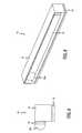
- a laser diode package 10includes a heat sink 12 , a laser diode bar 14 , and a lower substrate 16 .
- the laser diode bar 14is attached to the heat sink 12 through a first solder layer 18 .
- the substrate 16is attached to the heat sink 12 through a second solder layer 20 .
- the laser diode bar 14may also include a bar solder layer 22 on its side which opposes the heat sink 12 . The method by which such a bar solder layer 22 is applied is described in detail with respect to FIGS. 8 - 11 .
- the laser diode bar 14has an emitting surface 24 at its upper end and a reflective surface 26 that opposes the emitting surface 24 .
- the height of the laser diode bar 14is defined as the distance between the emitting surface 24 and reflective surface 26 .
- the junction of the laser diode 14which is the region at which the photons are emitted from the laser diode bar 14 , is typically closer to the heat sink 12 . However, the junction of the laser diode bar 14 can be closer to the exposed end of the laser diode bar 14 on which the solder layer 22 is placed. Electrical power is guided to defined regions of the junctions by providing electrically conductive material within the laser diode bar 14 adjacent those emitting regions and less electrically conductive material outside those regions.
- the laser diode bar 14has a multitude of emission points on the emitting surface 24 corresponding to those regions where electrical energy is converted into optical energy.
- the photonspropagate through the junction, are reflected off the reflective surface 26 , and consequently emit only from the emitting surface 24 in a direction perpendicular to it.
- the heat sink 12 of the laser diode package 10is made of a material that is both electrically and thermally conductive, such as copper. Electrical conductivity is required to conduct the electrical current through the laser diode bar 14 to produce the optical energy. Thermal conductivity is needed to conduct the intense heat away from the laser diode bar 14 and maintain the laser diode bar 14 at a reasonable operating temperature.
- the substrate 16serves the function of electrically isolating the current-conducting heat sink 12 from the ultimate heat sink, which is typically a metallic heat exchanger.
- the substrate 16can be a variety of materials which are electrically insulative.
- the substrate 16is made of semi-insulating or undoped gallium arsenide (“GaAs”). While GaAs is also a hazardous material, it can be cleaved to make the substrates which eliminates the need for any mechanical processes resulting in dust particles.
- GaAsgallium arsenide
- the substrate 16 made of an electrically insulative material, such as GaAsmust have a metalization layer if its surface is to be soldered.
- the substrate 16is made of GaAs, it can be cleaved such that its dimensional tolerances are very small (e.g. ⁇ 2-3 microns) such that its width can be approximately the same width of the heat sink 12 .
- Substrates made from GaAscan be made by polishing a wafer of GaAs to the desired thickness and cleaving the wafer into numerous substrates. The polished thickness of the wafer corresponds to the height of the substrate 16 that is present below the second solder layer 20 as shown in FIG. 1. If the substrate 16 is to be soldered, it is metallized after being polished. For example, the GaAs substrate 16 has a height in the range from about 0.003 inch to about 0.006 inch.
- the thermal resistance between the lowermost surface of the heat sink 12 and the ultimate thermal heat sinkis very small. Further, when the electrically insulative substrate 16 is made this thin, the overall height of the package 10 can be reduced as well.
- the substrate 16is preferably made of cleavable GaAs
- the substrate 16may be made of other electrically insulative materials, such as diamond, boron nitride, silicon, or aluminum nitride, which have a high thermal conductivity.
- the substrate 16could be made of beryllium oxide. Also, it is possible to attach the substrate 16 to the heat sink 12 with an adhesive.
- the lowermost surface of the heat sink 12with an electrically insulative coating, such as silicon oxide. Such a coating would make the heat sink 12 and substrate 16 integral while providing adequate electrical insulation and minimal thermal resistance. Further, it is also possible to make the heat sink 14 from an electrically nonconductive base material which has a metallic region, such as a solder coating over its uppermost surface, for conducting the electrical current through the laser diode bar 14 .
- the heat sinks 12 of the laser diode packages 10are preferably manufactured in such a way to have the material for the solder layers 18 and 20 on their exterior surface (i.e. “pretinned”).
- the heat sinks 12which are preferably copper, are dipped into a rosin based flux to prepare their exterior surfaces for being coated with a solder layer.
- the fluxis preferably an activated rosin flux such as Alpha No. 809 flux manufactured by the Alpha Metals of Jersey City, N.J.
- the heat sinks 12After the heat sinks 12 have been dipped into the flux, they are then dipped into molten indium which results in a solder layer on their exterior surfaces.
- the end surfaces of the heat sinks 12are placed on a hot plate which maintains their temperature above the melting point of indium ( ⁇ 157° C.) so that the excess indium can be blown from the exterior surfaces with air.
- the excess soldercan be removed through a solder wick material, such as mesh copper fibers.
- the heat sinks 12once removed from the molten indium, are subjected to a hot air source which has a temperature above the melting point of the indium. This eliminates the need for a hot plate.
- the goalis to provide a relatively even thickness of the indium solder layer.
- the solder layer on the exterior surface of each heat sink 12has a thickness of about 1-5 mils (about 0.001 inch to about 0.005 inch).
- the heat sinks 12are dipped into acetone to remove any additional flux that may be present on their exterior surfaces.
- the heat sinks 12are then stored in an environment where oxidation of the indium is inhibited.
- One example of such an environmentis a hexane bath into which the heat sinks 12 are submerged.
- the heat sinks 12may be dipped into a flux cleaning solution followed by immersion into an antioxidation solution. Both of these solutions are manufactured by Kester Solder Corporation of Des Plaines, Ill.
- the first and second solder layers 18 and 20can be produced by a single solder layer present on the entire heat sink 12 .
- the figuresdo not illustrate a constant layer of solder around the heat sinks 12 , but only reveal the existence of such a solder layer in areas where a solder bond exists.
- the individual who is assembling the laser diode package 10can determine whether the emitting surface 24 of the laser diode bar 14 extends too far above or too far below the upper surfaces of the heat sink 12 . If the emitting surface 24 is located too far above the heat sink 12 , there is no place for the heat produced on the upper portion of the laser diode bar 14 adjacent to the emitting surface 24 to be conducted which is one of the primary purposes of the heat sink 12 . If this is the case, then it is likely that the laser diode bar 14 will catastrophically fail due to an extreme temperature condition.
- the emitting surface 24 of the laser diode bar 14is positioned too far below the upper surface of the heat sink 12 , then the output energy of the laser diode bar 14 may be reduced due to the fact that the side surface of the heat sink 12 facing the laser diode bar 14 will absorb or undesirably reflect the emitting energy which causes a reduction in the output of laser diode bar 14 . Consequently, it is preferred that the emitting surface 24 be positioned substantially flush (i.e. substantially coplanar) with the upper surfaces of the heat sink 12 . In the preferred embodiment, the emitting surface 24 is positioned within about 1 mil (i.e. ⁇ 0.001 inch) of the upper surfaces of the heat sink 12 .
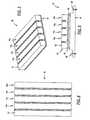
- a laser diode array 30which includes four laser diode packages 10 a, 10 b, 10 c, 10 d. These laser diode packages 10 are configured in the manner shown with respect to FIGS. 1 and 2.
- the laser diode array 30also includes an end heat sink 32 which mates against the laser diode bar 14 of the laser diode package 10 d.
- the end heat sink 32is no different than the heat sink 12 shown in FIGS. 1 and 2 except for the fact that it is not packaged with a laser diode bar.
- RA fluxrosin-activated flux
- the bar solder layer 22is preferably made of a lower melting temperature solder than the first solder layer 18 and the second solder layer 20 such that the heating process to liquefy the bar solder layer 22 does not also liquefy the first and second solder layers 18 and 20 .
- a solder layersuch as pure indium, as described above.
- the solder layer 22may be an indium alloy solder with a melting point of 143° C.
- the solder layer 22 on the laser diode bar 14adheres to the pure indium that is present on the heat sink 12 .
- the laser diode array 30is then cleaned by immersion in a heated acetone bath after which the laser diode array 30 is stored in a low humidity environment (e.g. a desiccant cabinet or a dry box). Alternatively, the laser diode array 30 can be subjected to a forced spray of acetone. Because the reflective surfaces 26 of the laser diode bars 14 in the packages 10 are exposed between adjacent heat sinks 12 , the reflective surfaces 26 of all of the laser diode bars 14 and, of course, the emitting surfaces 22 can be cleaned in this cleaning step. Also, while the multi-bar array 30 has been described, a single package 10 can be made integral with a free heat sink (i.e. like heat sink 32 ) to make a one bar array.
- FIG. 4is a top view of the laser diode array 30 of FIG. 3 which illustrates the relative dimensions of the heat sink 12 and the diode bar 14 .
- Each heat sink 12has a width of less than about 0.2 inch, and preferably about 0.12 inch, and a length of about 0.4 inch.
- the height of each heat sink 12is about 45 mils (0.045 inch), as shown in FIG. 3, before being dipped in the molten solder that produces the solder layers 18 and 20 . After being dipped, the height is about 50 mils (0.050 inch).
- the overall height of the package 10is about 50-60 mils (0.050 inch to 0.060 inch).
- the laser diode bar 14has a width of approximately 5 mils (0.005 inch) and the height of the laser diode bar 14 is usually about 20-25 mils (0.020 inch to 0.025 inch). Also, if the array 30 is to be operated in a pulsed mode, the width of the heat sinks 12 can be reduced since the average waste heat produced is less. For example, the heat sink 12 may have a width of only about 0.005 inch to about 0.02 inch for pulsed mode arrays.
- FIG. 5illustrates a laser diode array assembly 33 with a laser diode array 30 and heat spreader structure 34 .
- the heat spreader structure 34generally includes a plurality of fasteners 36 to attach the entire assembly to a heat exchanger positioned therebelow.
- the heat spreader 34is typically made of highly thermal conductive material such as copper.
- a substrate solder layer 38is located between the substrate 16 of each package 10 and the heat spreader 34 .
- the substrate solder layer 38is preferably made of a lower temperature solder than the other solder layers present in the laser diode package 10 .
- the bar solder layer 22 and the substrate solder layer 38can be made of the same material such that the heating of the overall assembly causes the two solder layers 22 and 38 to liquefy and, after cooling, form the integral unit.
- each individual substrate 16 of the array 30is spaced away from adjacent substrates 16 such that its side surfaces are free from contact adjacent substrates 16 .
- each laser diode bar 14 of the laser diode array 30To create optical energy, electrical current must be conducted through each laser diode bar 14 of the laser diode array 30 .
- the electrical currentflows into the heat sink of the first package 10 a, into the adjacent laser diode, and continues through each package 10 before exiting through the free heat sink 32 .
- the laser diode 14inherently includes some curvature along its length. Because of this inherent curvature, the distance from the exterior surfaces of the laser diode bar 14 to the surfaces of the adjacent heat sinks 12 will vary as a function of the length of laser diode bar 14 . This resulting gap between the laser diode bar 14 and the heat sinks, which varies in size, is filled with the appropriate thickness of solder such that contact with the heat sinks is established along the entire length of the laser diode bar 14 .
- the process by which the laser diode array 30 is assembledtends to provide a constant electrical contact along the entire length of the laser diode bars 14 even though the laser diode bar 14 has an inherent curvature which could normally produce voids in the solder contact.
- additional soldercan be added to fill in these voids to maintain the appropriate electrical and thermal contact along the entire length of the laser diode bar 14 .
- FIGS. 6 and 7illustrate a laser diode array assembly 40 which includes the laser diode array 30 attached directly to a heat exchanger 41 .
- This configurationis different than the assembly shown in FIG. 5 in that no heat spreader 34 is present as the laser diode array 30 is soldered directly onto the ultimate heat sinking reservoir, the heat exchanger 41 .
- the heat exchanger 41includes mounting sections 42 , each of which includes a bore 43 for passage of a fastener.
- the internal fins (not shown) of the heat exchanger 41are located within the body 44 of the heat exchanger 41 . Fluid passes into the body 44 through an inlet 46 and the fluid is discharged from the body 44 through an outlet 48 .
- the side of the body 44includes a contact 50 for receiving the requisite electrical input energy.
- the contact 50includes two leads 52 for connecting the heat sink 12 of the first laser diode package 10 a to the top contact 50 and the free end heat sink 32 to the bottom contact 50 .
- Each of the contacts 52are electrically insulated on their surfaces contacting the body 44 of the heat exchanger 40 to ensure current flows only into the laser diode array 30 .
- FIGS. 8 - 11illustrate the two steps by which the bar solder layer 22 is applied to the laser diode bar 14 .
- a solder deposit 22 ais placed on a portion of the laser diode bar 14 .
- the entire laser diode package 10can be heated to the point above the solder melting point of the solder deposit 22 a.
- the solder deposit 22 ais placed on a laser diode bar 14 , the goal is to spread the solder deposit 22 a evenly along the entire length of the laser diode bar 14 to create a thin solder layer. Because of the existence of the first and second solder layers 18 and 20 in the laser diode package 10 , the solder for the solder deposit 22 a is chosen to have a lower melting temperature than the first and second solder layers 18 and 20 .
- a wetting structure 54which can be simply a piece of copper foil, is placed at a location where it engages the solder deposit 22 a. Due to capillary action, the solder deposit 22 a begins to move along the length of the wetting structure 54 so as to cover the entire laser diode bar 14 . While this wetting structure 54 is performing its function, heat is being applied to the laser diode package 10 to maintain the solder deposit 22 a in its liquid form.
- One method by which the entire assembly is heatedis by placing the lower surface of the substrate 16 against a heating plate. The wetting structure 54 is moved away from the laser diode bar 14 while the solder layer 22 is still in its liquid form.
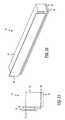
- FIGS. 12 - 14illustrate an alternative laser diode package 60 which includes structure for mounting a lens.
- the laser diode package 60includes a heat sink 62 , a laser diode bar 64 and a substrate 66 , just as in the configurations shown in FIGS. 1 and 2.
- the laser diode bar 64 and the substrate 66are soldered to the heat sink 62 in a similar manner described with reference to FIGS. 1 and 2.
- the laser diode bar 64preferably has a bar solder layer 72 applied to its exposed side in the manner described with reference to FIGS. 8 - 11 .
- the heat sink 62includes at each end a lens mount 74 which extends upwardly in the direction away from the substrate 66 .
- the lens mount 74further includes two flat surfaces 76 which receive an ultra-violet radiation (“UV”) activated adhesive.
- UVultra-violet radiation
- FIG. 15illustrates a laser diode array 80 which includes a plurality of lenses 82 .
- the laser diode array 80is comprised of five laser diode packages 60 a, 60 b, 60 c, 60 d, and 60 e, as described with reference to FIGS. 12 - 14 .
- Adjacent to the laser diode package 60 eis a free heat sink 84 which is soldered to the laser diode bar within the laser diode package 60 e.
- the free heat sink 84also includes the lens mount structure as described with reference to FIGS. 12 - 14 .
- Each of the lenses 82bridges two adjacent heat sinks 62 (FIGS.
- the laser diode array 80can produce a variety of laser beam outputs depending upon the type of lens 82 that is employed. It should be noted that the UV radiation can be exposed to the entire laser diode array 80 , instead of each package 60 , to activate the UV-activated radiation and secure the array of lenses 82 in their final state.
- FIG. 16illustrates a cross-section of an alternative laser diode array assembly 90 which has the laser diode array 30 mounted on the heat spreader 34 , as described previously in FIG. 5, with potting material placed entirely therearound.
- a first potting material 92is present along the sides of the laser diode arrays 30 and on the front and back faces (i.e. in the plane of the paper) of the laser diode array 30 .
- the potting material 92can also be present between adjacent heat sinks of the packages.
- a second potting material 94 that is transparent to the optical energy being emitted from the laser diode array 30is at the top of the laser diode array 30 .
- the potting materials 92 and 94can be made of various materials including, for example, an RTV.
- Two leads 96extend from the outer heat sinks through the potting material 92 .
- the only portions of the laser diode array assembly 90 which are exposed to the environmentare the two leads 96 and the bottom of the heat spreader 34 .
- This laser diode array assembly 90can be used in a variety of atmospheres which would normally contaminate the laser diode array 30 .
- placing potting material 92 around the heat sinks 12 which conduct the electrical currentcan minimize the chance for current arcing between the heat sinks 12 and the metallic heat spreader 34 positioned below it. Minimizing the chances for current arcing is especially important in arrays having large numbers of laser diodes where higher voltages are required to produce the desired optical output.
Landscapes
- Physics & Mathematics (AREA)
- Condensed Matter Physics & Semiconductors (AREA)
- General Physics & Mathematics (AREA)
- Electromagnetism (AREA)
- Optics & Photonics (AREA)
- Semiconductor Lasers (AREA)
Abstract
Description
- The present invention relates generally to lasers diodes and, in particular, to a package for a laser diode that is easy to manufacture, has a low thermal resistance, and requires no beryllium oxide.[0001]
- Semiconductor laser diodes have numerous advantages. They are small in that the widths of their active regions are typically submicron to a few microns and their heights are usually no more than a fraction of a millimeter. The length of their active regions is typically less than about a millimeter. The internal reflective surfaces, which produce emission in one direction, are formed by cleaving the substrate from which the laser diodes are produced and, thus, have high mechanical stability.[0002]
- High efficiencies are possible with semiconductor laser diodes with some pulsed junction laser diodes having external quantum efficiencies near 50%. Semiconductor lasers produce radiation at wavelengths from about 20 to about 0.7 microns depending on the semiconductor alloy that is used. For example, laser diodes made of gallium arsenide with aluminum doping (AlGaAs) emit radiation at approximately 0.8 microns (˜800 nm) which is near the absorption spectrum of common solid state laser rods and slabs made from Neodymium doped, Yttrium-Aluminum Garnet (Nd:YAG), and other crystals and glasses. Thus, semiconductor laser diodes can be used as the optical pumping source for larger, solid state laser systems.[0003]
- Universal utilization of semiconductor laser diodes has been restricted by thermally related problems. These problems are associated with the large heat dissipation per unit area of the laser diodes which results in elevated junction temperatures and stresses induced by thermal cycling. Laser diode efficiency and the service life of the laser diode is decreased as the operating temperature in the junction increases.[0004]
- Furthermore, the emitted wavelength of a laser diode is a function of its junction temperature. Thus, when a specific output wavelength is desired, maintaining a constant junction temperature is essential. For example, AlGaAs laser diodes that are used to pump a Nd:YAG rod or slab should emit radiation at about 808 nm since this is the wavelength at which optimum energy absorption exists in the Nd:YAG. But, for every 3.5° C. to 4.0° C. deviation in the junction temperature of the AlGaAs laser diode, the wavelength shifts 1 nm. Accordingly, controlling the junction temperature and, thus, properly dissipating the heat is critical.[0005]
- When solid state laser rods or slabs are pumped by laser diodes, dissipation of the heat becomes more problematic since it becomes necessary to densely pack a plurality of individual diodes into arrays which generate the required amounts of input power for the larger, solid state laser rod or slab. However, when the packing density of the individual laser diodes is increased, the space available for extraction of heat from the individual laser diodes decreases. This aggravates the problem of heat extraction from the arrays of individual diodes.[0006]
- To remove heat from the laser diodes, some laser diode array packages have used beryllium oxide which has a relatively high thermal conductivity while being electrically insulative. One known commercially available package which attempts to resolve these thermally-related problems by use of beryllium oxide is produced by Laser Diode Array Inc. of Auburn, N.Y. This package generally includes a beryllium oxide structure into which a plurality of grooves are cut, etched or sawed. A metallized layer extends from groove to groove to conduct electricity through the laser diodes that are within the grooves.[0007]
- However, beryllium oxide is a hazardous material and requires additional care in handling. This is especially true when the beryllium oxide is being mechanically processed (e.g. cutting or sawing) which produces airborne particles of the beryllium oxide. Because it requires additional care in handling and shipping (e.g. additional BeO warning labels), it is relatively expensive when considering the cost of the overall laser diode array package. Additionally, once the laser diode bar is placed within the groove, its reflective surface is not accessible for cleaning after the array has been assembled. Furthermore, it is difficult to test an individual laser diode bar before it is placed in the grooves. Thus, a laser diode bar lacking the desired operational characteristics for a specific array must often be removed from a groove after it has been installed.[0008]
- A need exists for a thermally efficient laser diode package which is easy to assemble and test, and which preferably lacks the hazardous beryllium oxide.[0009]
- The present invention solves the aforementioned problems by providing a laser diode package that includes a heat sink, a laser diode, and an electrically nonconductive (i.e. insulative) substrate. The laser diode has an emitting surface and a reflective surface opposing the emitting surface. The laser diode further has first and second side surfaces between the emitting and reflective surfaces. The heat sink has an upper surface and a lower surface. The first side surface of the laser diode is attached to the heat sink adjacent to the upper surface of the heat sink. The substrate is attached to the lower surface of the heat sink.[0010]
- Preferably, the heat sink is made of heat conducting metal such as copper and the substrate is primarily made from gallium arsenide. The substrate is soldered to the heat sink as is the laser diode. In one embodiment, the heat sink is coated with a layer of solder such that at least its surfaces that will contact the laser diode and the substrate are “pretinned.” The laser diode and substrate are then attached to the heat sink during one soldering step in which the heat sink is heated above the melting point of the solder layer on its surface.[0011]
- The exposed second side surface of the laser diode preferably includes a layer of solder so that two packages can be joined. Accordingly, the heat sink of a first package is placed in contact with the laser diode bar of a second adjacent package. The packages are then heated to a point where the solder layer on the laser diode reflows and the laser diode of the second package becomes integral with the heat sink of the adjacent first package. To avoid reflowing all solder present in the package, the solder layer on the laser diode is a lower melting temperature solder than the other resident solders of the package. Numerous individual packages can be made integral in such a fashion resulting in a multi-bar laser diode array.[0012]
- A laser diode package and a laser diode array that are constructed in this manner lack the hazardous beryllium oxide. More importantly, each individual package has its own electrical isolation and can be directly soldered to an ultimate heat sink. Furthermore, each individual package can be tested on its own before being placed in an array to ensure that it will function within the operational parameters (e.g. wavelength and power) desired for such an array. When the substrate is made of a cleaveable material such as GaAs, it can be produced with relatively small dimensions thereby minimizing the thermal resistance between the laser diode and the ultimate heat sink. The resulting laser diode package can be used for continuous wave (CW) modes of operation or for pulsed modes of operation.[0013]
- The above summary of the present invention is not intended to represent each embodiment, or every aspect, of the present invention. This is the purpose of the figures and the detailed description which follow.[0014]
- Other objects and advantages of the invention will become apparent upon reading the following detailed description and upon reference to the drawings in which:[0015]
- FIG. 1 is an end view of the inventive laser diode package;[0016]
- FIG. 2 is a perspective view of the inventive laser diode package;[0017]
- FIG. 3 is a perspective view of a laser diode array comprised of the laser diode packages of FIGS. 1 and 2;[0018]
- FIG. 4 is a top view of the laser diode array of FIG. 3;[0019]
- FIG. 5 is an end view of the laser diode array of FIG. 3 including a heat spreader for mounting the laser diode array;[0020]
- FIG. 6 is a perspective view of the laser diode array mounted on a heat exchanger;[0021]
- FIG. 7 is an end view of FIG. 6;[0022]
- FIG. 8 is a perspective view of the laser diode package of FIG. 1 during assembly;[0023]
- FIG. 9 is an end view of FIG. 8;[0024]
- FIG. 10 is a perspective view of the laser diode package of FIG. 1 during assembly;[0025]
- FIG. 11 is an end view of FIG. 10;[0026]
- FIG. 12 is a perspective view of an alternative laser diode package for use with a collimating lens;[0027]
- FIG. 13 is an end view of FIG. 12;[0028]
- FIG. 14 is a side view of FIG. 12;[0029]
- FIG. 15 is a laser diode array assembly with a plurality of collimating lens mounted thereto; and[0030]
- FIG. 16 is a cross-sectional view of a laser diode array having potting material present therearound.[0031]
- While the invention is susceptible to various modifications and alternative forms, a specific embodiment thereof has been shown by way of example in the drawings and will herein be described in detail. It should be understood, however, that it is not intended to limit the invention to the particular forms disclosed. To the contrary, the intention is to cover all modifications, equivalents, and alternatives falling within the spirit and scope of the invention as defined by the appended claims.[0032]
- Referring initially to FIGS. 1 and 2, a[0033]
laser diode package 10 includes aheat sink 12, alaser diode bar 14, and alower substrate 16. Thelaser diode bar 14 is attached to theheat sink 12 through afirst solder layer 18. Thesubstrate 16 is attached to theheat sink 12 through asecond solder layer 20. Thelaser diode bar 14 may also include abar solder layer 22 on its side which opposes theheat sink 12. The method by which such abar solder layer 22 is applied is described in detail with respect to FIGS.8-11. - The[0034]
laser diode bar 14 has an emittingsurface 24 at its upper end and areflective surface 26 that opposes the emittingsurface 24. The height of thelaser diode bar 14 is defined as the distance between the emittingsurface 24 andreflective surface 26. The junction of thelaser diode 14, which is the region at which the photons are emitted from thelaser diode bar 14, is typically closer to theheat sink 12. However, the junction of thelaser diode bar 14 can be closer to the exposed end of thelaser diode bar 14 on which thesolder layer 22 is placed. Electrical power is guided to defined regions of the junctions by providing electrically conductive material within thelaser diode bar 14 adjacent those emitting regions and less electrically conductive material outside those regions. Thus, thelaser diode bar 14 has a multitude of emission points on the emittingsurface 24 corresponding to those regions where electrical energy is converted into optical energy. When the electrical power is applied to thelaser diode package 10, the photons propagate through the junction, are reflected off thereflective surface 26, and consequently emit only from the emittingsurface 24 in a direction perpendicular to it. - The[0035]
heat sink 12 of thelaser diode package 10 is made of a material that is both electrically and thermally conductive, such as copper. Electrical conductivity is required to conduct the electrical current through thelaser diode bar 14 to produce the optical energy. Thermal conductivity is needed to conduct the intense heat away from thelaser diode bar 14 and maintain thelaser diode bar 14 at a reasonable operating temperature. - The[0036]
substrate 16 serves the function of electrically isolating the current-conductingheat sink 12 from the ultimate heat sink, which is typically a metallic heat exchanger. Thesubstrate 16 can be a variety of materials which are electrically insulative. In a preferred embodiment, thesubstrate 16 is made of semi-insulating or undoped gallium arsenide (“GaAs”). While GaAs is also a hazardous material, it can be cleaved to make the substrates which eliminates the need for any mechanical processes resulting in dust particles. Thesubstrate 16 made of an electrically insulative material, such as GaAs, must have a metalization layer if its surface is to be soldered. - Further, if the[0037]
substrate 16 is made of GaAs, it can be cleaved such that its dimensional tolerances are very small (e.g. ±2-3 microns) such that its width can be approximately the same width of theheat sink 12. Substrates made from GaAs can be made by polishing a wafer of GaAs to the desired thickness and cleaving the wafer into numerous substrates. The polished thickness of the wafer corresponds to the height of thesubstrate 16 that is present below thesecond solder layer 20 as shown in FIG. 1. If thesubstrate 16 is to be soldered, it is metallized after being polished. For example, theGaAs substrate 16 has a height in the range from about 0.003 inch to about 0.006 inch. Because the height is so small, the thermal resistance between the lowermost surface of theheat sink 12 and the ultimate thermal heat sink (e.g. a heat exchanger) is very small. Further, when theelectrically insulative substrate 16 is made this thin, the overall height of thepackage 10 can be reduced as well. - While the[0038]
substrate 16 is preferably made of cleavable GaAs, thesubstrate 16 may be made of other electrically insulative materials, such as diamond, boron nitride, silicon, or aluminum nitride, which have a high thermal conductivity. Further, thesubstrate 16 could be made of beryllium oxide. Also, it is possible to attach thesubstrate 16 to theheat sink 12 with an adhesive. - It is also possible to provide the lowermost surface of the[0039]
heat sink 12 with an electrically insulative coating, such as silicon oxide. Such a coating would make theheat sink 12 andsubstrate 16 integral while providing adequate electrical insulation and minimal thermal resistance. Further, it is also possible to make theheat sink 14 from an electrically nonconductive base material which has a metallic region, such as a solder coating over its uppermost surface, for conducting the electrical current through thelaser diode bar 14. - The heat sinks[0040]12 of the laser diode packages10 are preferably manufactured in such a way to have the material for the solder layers18 and20 on their exterior surface (i.e. “pretinned”). First, the heat sinks12, which are preferably copper, are dipped into a rosin based flux to prepare their exterior surfaces for being coated with a solder layer. The flux is preferably an activated rosin flux such as Alpha No. 809 flux manufactured by the Alpha Metals of Jersey City, N.J. After the heat sinks12 have been dipped into the flux, they are then dipped into molten indium which results in a solder layer on their exterior surfaces. Next, the end surfaces of the heat sinks12 are placed on a hot plate which maintains their temperature above the melting point of indium (˜157° C.) so that the excess indium can be blown from the exterior surfaces with air. Alternatively, the excess solder can be removed through a solder wick material, such as mesh copper fibers. In a further alternative, the heat sinks12, once removed from the molten indium, are subjected to a hot air source which has a temperature above the melting point of the indium. This eliminates the need for a hot plate. In these alternative processing steps, the goal is to provide a relatively even thickness of the indium solder layer. Preferably, the solder layer on the exterior surface of each
heat sink 12 has a thickness of about 1-5 mils (about 0.001 inch to about 0.005 inch). - Once the excess indium is removed and the desired indium thickness is achieved, the heat sinks[0041]12 are dipped into acetone to remove any additional flux that may be present on their exterior surfaces. The heat sinks12 are then stored in an environment where oxidation of the indium is inhibited. One example of such an environment is a hexane bath into which the heat sinks12 are submerged. Alternatively, the heat sinks12 may be dipped into a flux cleaning solution followed by immersion into an antioxidation solution. Both of these solutions are manufactured by Kester Solder Corporation of Des Plaines, Ill.
- Consequently, the first and second solder layers[0042]18 and20 can be produced by a single solder layer present on the
entire heat sink 12. This eliminates the need to accurately locate individual solder layers for interfacing with thelaser diode bar 14 and thesubstrate 16 although such a methodology will also perform the desired function. It should be noted that the figures do not illustrate a constant layer of solder around the heat sinks12, but only reveal the existence of such a solder layer in areas where a solder bond exists. - During the assembly process, the individual who is assembling the[0043]
laser diode package 10 can determine whether the emittingsurface 24 of thelaser diode bar 14 extends too far above or too far below the upper surfaces of theheat sink 12. If the emittingsurface 24 is located too far above theheat sink 12, there is no place for the heat produced on the upper portion of thelaser diode bar 14 adjacent to the emittingsurface 24 to be conducted which is one of the primary purposes of theheat sink 12. If this is the case, then it is likely that thelaser diode bar 14 will catastrophically fail due to an extreme temperature condition. On the other hand, if the emittingsurface 24 of thelaser diode bar 14 is positioned too far below the upper surface of theheat sink 12, then the output energy of thelaser diode bar 14 may be reduced due to the fact that the side surface of theheat sink 12 facing thelaser diode bar 14 will absorb or undesirably reflect the emitting energy which causes a reduction in the output oflaser diode bar 14. Consequently, it is preferred that the emittingsurface 24 be positioned substantially flush (i.e. substantially coplanar) with the upper surfaces of theheat sink 12. In the preferred embodiment, the emittingsurface 24 is positioned within about 1 mil (i.e. ±0.001 inch) of the upper surfaces of theheat sink 12. - Referring now to FIG. 3, a[0044]
laser diode array 30 is illustrated which includes four laser diode packages10a,10b,10c,10d.These laser diode packages10 are configured in the manner shown with respect to FIGS. 1 and 2. Thelaser diode array 30 also includes anend heat sink 32 which mates against thelaser diode bar 14 of thelaser diode package 10d.Theend heat sink 32 is no different than theheat sink 12 shown in FIGS. 1 and 2 except for the fact that it is not packaged with a laser diode bar. - To attach each heat sink of a[0045]
laser diode package 10 to the diode bar of the adjacentlaser diode package 10, the laser diode bars14 of thelaser diode array 30 are subjected to a rosin-activated flux (“RA flux”) which assists in adhering thesolder layer 22 to the adjacent heat sinks. The packages are then heated to the point where the bar solder layer22 (FIGS. 1 and 2) liquefies (e.g. ˜157° C. when pure indium is used). To this end, thebar solder layer 22 is preferably made of a lower melting temperature solder than thefirst solder layer 18 and thesecond solder layer 20 such that the heating process to liquefy thebar solder layer 22 does not also liquefy the first and second solder layers18 and20. This is especially needed when theheat sink 12 has been entirely coated with a solder layer, such as pure indium, as described above. For example, thesolder layer 22 may be an indium alloy solder with a melting point of 143° C. Once the heat which causes the reflow of thesolder layer 22 is removed, thesolder layer 22 again solidifies to produce one integral unit as is shown in FIG. 3. When theheat sink 12 is pretinned with pure indium on its exterior surfaces, thesolder layer 22 on thelaser diode bar 14 adheres to the pure indium that is present on theheat sink 12. Thelaser diode array 30 is then cleaned by immersion in a heated acetone bath after which thelaser diode array 30 is stored in a low humidity environment (e.g. a desiccant cabinet or a dry box). Alternatively, thelaser diode array 30 can be subjected to a forced spray of acetone. Because thereflective surfaces 26 of the laser diode bars14 in thepackages 10 are exposed betweenadjacent heat sinks 12, thereflective surfaces 26 of all of the laser diode bars14 and, of course, the emittingsurfaces 22 can be cleaned in this cleaning step. Also, while themulti-bar array 30 has been described, asingle package 10 can be made integral with a free heat sink (i.e. like heat sink32) to make a one bar array. - FIG. 4 is a top view of the[0046]
laser diode array 30 of FIG. 3 which illustrates the relative dimensions of theheat sink 12 and thediode bar 14. Eachheat sink 12 has a width of less than about 0.2 inch, and preferably about 0.12 inch, and a length of about 0.4 inch. The height of eachheat sink 12 is about 45 mils (0.045 inch), as shown in FIG. 3, before being dipped in the molten solder that produces the solder layers18 and20. After being dipped, the height is about 50 mils (0.050 inch). Considering the height of thesubstrate 16 is only about 3 mils to about 6 mils when GaAs is used, the overall height of thepackage 10 is about 50-60 mils (0.050 inch to 0.060 inch). Thelaser diode bar 14 has a width of approximately 5 mils (0.005 inch) and the height of thelaser diode bar 14 is usually about 20-25 mils (0.020 inch to 0.025 inch). Also, if thearray 30 is to be operated in a pulsed mode, the width of the heat sinks12 can be reduced since the average waste heat produced is less. For example, theheat sink 12 may have a width of only about 0.005 inch to about 0.02 inch for pulsed mode arrays. - FIG. 5 illustrates a laser[0047]
diode array assembly 33 with alaser diode array 30 andheat spreader structure 34. Theheat spreader structure 34 generally includes a plurality offasteners 36 to attach the entire assembly to a heat exchanger positioned therebelow. Theheat spreader 34 is typically made of highly thermal conductive material such as copper. - To attach the[0048]
laser diode array 30 to theheat spreader 34, asubstrate solder layer 38 is located between thesubstrate 16 of eachpackage 10 and theheat spreader 34. To ensure that the solder layers18,20, and22 of eachlaser diode package 10 do not liquefy during attachment, thesubstrate solder layer 38 is preferably made of a lower temperature solder than the other solder layers present in thelaser diode package 10. Alternatively, if thelaser diode array 30 is to be assembled from the laser diode packages10 at the same time as thelaser diode array 30 is attached to theheat spreader 34, thebar solder layer 22 and thesubstrate solder layer 38 can be made of the same material such that the heating of the overall assembly causes the twosolder layers individual substrate 16 of thearray 30 is spaced away fromadjacent substrates 16 such that its side surfaces are free from contactadjacent substrates 16. - To create optical energy, electrical current must be conducted through each[0049]
laser diode bar 14 of thelaser diode array 30. When viewing thelaser diode array 30 from left to right in FIGS.3 or5, the electrical current flows into the heat sink of thefirst package 10a,into the adjacent laser diode, and continues through eachpackage 10 before exiting through thefree heat sink 32. There is no electrical path below eachlaser diode package 10 due to thesubstrate 16. It is this electrical current through thelaser diodes 12 that produces the optical energy from thelaser diode assembly 10. - It should be noted that due to the manufacturing process by which the[0050]
laser diode bar 14 is produced, thelaser diode 14 inherently includes some curvature along its length. Because of this inherent curvature, the distance from the exterior surfaces of thelaser diode bar 14 to the surfaces of theadjacent heat sinks 12 will vary as a function of the length oflaser diode bar 14. This resulting gap between thelaser diode bar 14 and the heat sinks, which varies in size, is filled with the appropriate thickness of solder such that contact with the heat sinks is established along the entire length of thelaser diode bar 14. In other words, the process by which thelaser diode array 30 is assembled tends to provide a constant electrical contact along the entire length of the laser diode bars14 even though thelaser diode bar 14 has an inherent curvature which could normally produce voids in the solder contact. Furthermore, it should be noted that even if voids appear adjacent to thelaser diode bar 14 after the assembly process, additional solder can be added to fill in these voids to maintain the appropriate electrical and thermal contact along the entire length of thelaser diode bar 14. - FIGS. 6 and 7 illustrate a laser[0051]
diode array assembly 40 which includes thelaser diode array 30 attached directly to aheat exchanger 41. This configuration is different than the assembly shown in FIG. 5 in that noheat spreader 34 is present as thelaser diode array 30 is soldered directly onto the ultimate heat sinking reservoir, theheat exchanger 41. Theheat exchanger 41 includes mountingsections 42, each of which includes abore 43 for passage of a fastener. The internal fins (not shown) of theheat exchanger 41 are located within thebody 44 of theheat exchanger 41. Fluid passes into thebody 44 through aninlet 46 and the fluid is discharged from thebody 44 through anoutlet 48. The side of thebody 44 includes acontact 50 for receiving the requisite electrical input energy. Thecontact 50 includes two leads52 for connecting theheat sink 12 of the firstlaser diode package 10ato thetop contact 50 and the freeend heat sink 32 to thebottom contact 50. Each of thecontacts 52 are electrically insulated on their surfaces contacting thebody 44 of theheat exchanger 40 to ensure current flows only into thelaser diode array 30. - FIGS.[0052]8-11 illustrate the two steps by which the
bar solder layer 22 is applied to thelaser diode bar 14. In FIGS. 8 and 9, asolder deposit 22ais placed on a portion of thelaser diode bar 14. At this point, the entirelaser diode package 10 can be heated to the point above the solder melting point of thesolder deposit 22a.Once thesolder deposit 22ais placed on alaser diode bar 14, the goal is to spread thesolder deposit 22aevenly along the entire length of thelaser diode bar 14 to create a thin solder layer. Because of the existence of the first and second solder layers18 and20 in thelaser diode package 10, the solder for thesolder deposit 22ais chosen to have a lower melting temperature than the first and second solder layers18 and20. - As shown in FIGS. 10 and 11, a wetting[0053]
structure 54, which can be simply a piece of copper foil, is placed at a location where it engages thesolder deposit 22a.Due to capillary action, thesolder deposit 22abegins to move along the length of the wettingstructure 54 so as to cover the entirelaser diode bar 14. While this wettingstructure 54 is performing its function, heat is being applied to thelaser diode package 10 to maintain thesolder deposit 22ain its liquid form. One method by which the entire assembly is heated is by placing the lower surface of thesubstrate 16 against a heating plate. The wettingstructure 54 is moved away from thelaser diode bar 14 while thesolder layer 22 is still in its liquid form. - FIGS.[0054]12-14 illustrate an alternative
laser diode package 60 which includes structure for mounting a lens. Thelaser diode package 60 includes aheat sink 62, alaser diode bar 64 and asubstrate 66, just as in the configurations shown in FIGS. 1 and 2. Thelaser diode bar 64 and thesubstrate 66 are soldered to theheat sink 62 in a similar manner described with reference to FIGS. 1 and 2. Thelaser diode bar 64 preferably has abar solder layer 72 applied to its exposed side in the manner described with reference to FIGS.8-11. - The[0055]
heat sink 62 includes at each end alens mount 74 which extends upwardly in the direction away from thesubstrate 66. The lens mount74 further includes twoflat surfaces 76 which receive an ultra-violet radiation (“UV”) activated adhesive. When a lens is placed in its final alignment position, thepackage 60 is exposed to UV radiation which activates the UV adhesive and holds the lens in its final position. - FIG. 15 illustrates a[0056]
laser diode array 80 which includes a plurality oflenses 82. Thelaser diode array 80 is comprised of five laser diode packages60a,60b,60c,60d,and60e,as described with reference to FIGS.12-14. Adjacent to the laser diode package60eis afree heat sink 84 which is soldered to the laser diode bar within the laser diode package60e.Thefree heat sink 84 also includes the lens mount structure as described with reference to FIGS.12-14. Each of thelenses 82 bridges two adjacent heat sinks62 (FIGS.12-14) such that its center point is approximately over the emission point of the laser diode bars. Thus, thelaser diode array 80 can produce a variety of laser beam outputs depending upon the type oflens 82 that is employed. It should be noted that the UV radiation can be exposed to the entirelaser diode array 80, instead of eachpackage 60, to activate the UV-activated radiation and secure the array oflenses 82 in their final state. - FIG. 16 illustrates a cross-section of an alternative laser diode array assembly[0057]90 which has the
laser diode array 30 mounted on theheat spreader 34, as described previously in FIG. 5, with potting material placed entirely therearound. Afirst potting material 92 is present along the sides of thelaser diode arrays 30 and on the front and back faces (i.e. in the plane of the paper) of thelaser diode array 30. The pottingmaterial 92 can also be present between adjacent heat sinks of the packages. Asecond potting material 94 that is transparent to the optical energy being emitted from thelaser diode array 30 is at the top of thelaser diode array 30. Thepotting materials - Two leads[0058]96 extend from the outer heat sinks through the potting
material 92. Thus, the only portions of the laser diode array assembly90 which are exposed to the environment are the two leads96 and the bottom of theheat spreader 34. This laser diode array assembly90 can be used in a variety of atmospheres which would normally contaminate thelaser diode array 30. Furthermore, placingpotting material 92 around the heat sinks12 which conduct the electrical current can minimize the chance for current arcing between the heat sinks12 and themetallic heat spreader 34 positioned below it. Minimizing the chances for current arcing is especially important in arrays having large numbers of laser diodes where higher voltages are required to produce the desired optical output. - Each of these embodiments and obvious variations thereof is contemplated as falling within the spirit and scope of the invention, which is set forth in the following claims.[0059]
Claims (72)
Priority Applications (2)
| Application Number | Priority Date | Filing Date | Title |
|---|---|---|---|
| US10/672,991US7060515B2 (en) | 1999-03-29 | 2003-09-26 | Method of manufacturing a laser diode package |
| US11/406,748US7361978B2 (en) | 1999-03-29 | 2006-04-18 | Laser diode packaging |
Applications Claiming Priority (2)
| Application Number | Priority Date | Filing Date | Title |
|---|---|---|---|
| US09/280,783US6636538B1 (en) | 1999-03-29 | 1999-03-29 | Laser diode packaging |
| US10/672,991US7060515B2 (en) | 1999-03-29 | 2003-09-26 | Method of manufacturing a laser diode package |
Related Parent Applications (1)
| Application Number | Title | Priority Date | Filing Date |
|---|---|---|---|
| US09/280,783DivisionUS6636538B1 (en) | 1999-03-29 | 1999-03-29 | Laser diode packaging |
Related Child Applications (1)
| Application Number | Title | Priority Date | Filing Date |
|---|---|---|---|
| US11/406,748DivisionUS7361978B2 (en) | 1999-03-29 | 2006-04-18 | Laser diode packaging |
Publications (2)
| Publication Number | Publication Date |
|---|---|
| US20040082112A1true US20040082112A1 (en) | 2004-04-29 |
| US7060515B2 US7060515B2 (en) | 2006-06-13 |
Family
ID=23074631
Family Applications (3)
| Application Number | Title | Priority Date | Filing Date |
|---|---|---|---|
| US09/280,783Expired - LifetimeUS6636538B1 (en) | 1999-03-29 | 1999-03-29 | Laser diode packaging |
| US10/672,991Expired - LifetimeUS7060515B2 (en) | 1999-03-29 | 2003-09-26 | Method of manufacturing a laser diode package |
| US11/406,748Expired - LifetimeUS7361978B2 (en) | 1999-03-29 | 2006-04-18 | Laser diode packaging |
Family Applications Before (1)
| Application Number | Title | Priority Date | Filing Date |
|---|---|---|---|
| US09/280,783Expired - LifetimeUS6636538B1 (en) | 1999-03-29 | 1999-03-29 | Laser diode packaging |
Family Applications After (1)
| Application Number | Title | Priority Date | Filing Date |
|---|---|---|---|
| US11/406,748Expired - LifetimeUS7361978B2 (en) | 1999-03-29 | 2006-04-18 | Laser diode packaging |
Country Status (5)
| Country | Link |
|---|---|
| US (3) | US6636538B1 (en) |
| EP (1) | EP1166411A1 (en) |
| JP (1) | JP3781970B2 (en) |
| AU (1) | AU4041700A (en) |
| WO (1) | WO2000059086A1 (en) |
Cited By (47)
| Publication number | Priority date | Publication date | Assignee | Title |
|---|---|---|---|---|
| WO2006122691A3 (en)* | 2005-05-13 | 2007-04-19 | Lasag Ag | Laser device formed by a stack of laser diodes |
| EP1811617A1 (en)* | 2006-01-18 | 2007-07-25 | JENOPTIK Laserdiode GmbH | Base for a vertical arrangement of laserdiode bars with a stop |
| EP1887666A2 (en) | 2006-08-10 | 2008-02-13 | Lasertel Inc. | Method and system for a laser diode bar array assembly |
| WO2008028622A1 (en)* | 2006-09-08 | 2008-03-13 | Limo Patentverwaltung Gmbh & Co. Kg | Laser apparatus |
| US20080087906A1 (en)* | 2005-02-25 | 2008-04-17 | Dowa Electronics Materials Co., Ltd. | Algaas-Based Light Emitting Diode Having Double Hetero Junction and Manufacturing Method of the Same |
| US20080192785A1 (en)* | 2007-02-13 | 2008-08-14 | Jurgen Schulz-Harder | Diode laser array and method for manufacturing such an array |
| US20090185274A1 (en)* | 2008-01-21 | 2009-07-23 | Prime Sense Ltd. | Optical designs for zero order reduction |
| US20090190619A1 (en)* | 2008-01-30 | 2009-07-30 | Shenzhen Century Epitech Photonics Technology Co. Ltd. | Semiconductor laser package |
| US20110188054A1 (en)* | 2010-02-02 | 2011-08-04 | Primesense Ltd | Integrated photonics module for optical projection |
| US8749796B2 (en) | 2011-08-09 | 2014-06-10 | Primesense Ltd. | Projectors of structured light |
| US8829406B2 (en) | 2009-11-15 | 2014-09-09 | Primesense Ltd. | Optical projector with beam monitor including sensing intensity of beam pattern not projected toward an object |
| US8908277B2 (en) | 2011-08-09 | 2014-12-09 | Apple Inc | Lens array projector |
| US9036158B2 (en) | 2010-08-11 | 2015-05-19 | Apple Inc. | Pattern projector |
| US9066087B2 (en) | 2010-11-19 | 2015-06-23 | Apple Inc. | Depth mapping using time-coded illumination |
| US9098931B2 (en) | 2010-08-11 | 2015-08-04 | Apple Inc. | Scanning projectors and image capture modules for 3D mapping |
| US9131136B2 (en) | 2010-12-06 | 2015-09-08 | Apple Inc. | Lens arrays for pattern projection and imaging |
| US9201237B2 (en) | 2012-03-22 | 2015-12-01 | Apple Inc. | Diffraction-based sensing of mirror position |
| US9239467B2 (en) | 2008-01-21 | 2016-01-19 | Apple Inc. | Optical pattern projection |
| US9528906B1 (en) | 2013-12-19 | 2016-12-27 | Apple Inc. | Monitoring DOE performance using total internal reflection |
| DE102015013511B3 (en)* | 2015-10-15 | 2017-03-16 | Jenoptik Laser Gmbh | Laser radiation source and method for producing a laser radiation source and use of a soldering process |
| US20170170628A1 (en)* | 2014-11-17 | 2017-06-15 | Fujikura Ltd. | Semiconductor laser apparatus and method of manufacturing the same |
| US9736459B2 (en) | 2010-02-02 | 2017-08-15 | Apple Inc. | Generation of patterned radiation |
| CN107196186A (en)* | 2017-06-16 | 2017-09-22 | 西安炬光科技股份有限公司 | A kind of heat sink insulated type semiconductor laser and its folded battle array |
| US9825425B2 (en) | 2013-06-19 | 2017-11-21 | Apple Inc. | Integrated structured-light projector comprising light-emitting elements on a substrate |
| US10012831B2 (en) | 2015-08-03 | 2018-07-03 | Apple Inc. | Optical monitoring of scan parameters |
| DE102017210602B3 (en) | 2017-06-23 | 2018-07-26 | Jenoptik Laser Gmbh | Diode laser with housing |
| US10073004B2 (en) | 2016-09-19 | 2018-09-11 | Apple Inc. | DOE defect monitoring utilizing total internal reflection |
| US10146009B2 (en) | 2013-07-04 | 2018-12-04 | Mellanox Technologies, Ltd. | Silicon photonics connector |
| US10153614B1 (en) | 2017-08-31 | 2018-12-11 | Apple Inc. | Creating arbitrary patterns on a 2-D uniform grid VCSEL array |
| CN109188823A (en)* | 2018-10-18 | 2019-01-11 | 华北水利水电大学 | A kind of laser array light source for optical scanner |
| US10541508B2 (en)* | 2017-06-23 | 2020-01-21 | Jenoptik Optical Systems Gmbh | Diode laser with housing |
| US10741995B2 (en)* | 2016-09-27 | 2020-08-11 | Jenoptik Optical Systems Gmbh | Optical and optoelectronic assembly and method for the production thereof |
| US10903618B2 (en)* | 2019-03-20 | 2021-01-26 | Chroma Ate Inc. | Fixture assembly for testing edge-emitting laser diodes and testing apparatus having the same |
| US10965096B2 (en)* | 2019-03-20 | 2021-03-30 | Chroma Ate Inc. | Fixture assembly for testing surface emitting laser diodes and testing apparatus having the same |
| US11056854B2 (en) | 2018-08-14 | 2021-07-06 | Leonardo Electronics Us Inc. | Laser assembly and related methods |
| US11296481B2 (en) | 2019-01-09 | 2022-04-05 | Leonardo Electronics Us Inc. | Divergence reshaping array |
| CN114825027A (en)* | 2021-01-29 | 2022-07-29 | 山东华光光电子股份有限公司 | Conduction cooling semiconductor laser packaging structure for pumping and packaging method thereof |
| US11406004B2 (en) | 2018-08-13 | 2022-08-02 | Leonardo Electronics Us Inc. | Use of metal-core printed circuit board (PCB) for generation of ultra-narrow, high-current pulse driver |
| US11422292B1 (en) | 2018-06-10 | 2022-08-23 | Apple Inc. | Super-blazed diffractive optical elements with sub-wavelength structures |
| US11506762B1 (en) | 2019-09-24 | 2022-11-22 | Apple Inc. | Optical module comprising an optical waveguide with reference light path |
| US11681019B2 (en) | 2019-09-18 | 2023-06-20 | Apple Inc. | Optical module with stray light baffle |
| US11705690B2 (en) | 2016-11-29 | 2023-07-18 | Leonardo Electronics Us Inc. | Dual junction fiber-coupled laser diode and related methods |
| US11752571B1 (en) | 2019-06-07 | 2023-09-12 | Leonardo Electronics Us Inc. | Coherent beam coupler |
| US11754767B1 (en) | 2020-03-05 | 2023-09-12 | Apple Inc. | Display with overlaid waveguide |
| CN118040459A (en)* | 2024-04-15 | 2024-05-14 | 苏州长光华芯光电技术股份有限公司 | Semiconductor packaging structure and packaging method |
| US12111421B2 (en) | 2021-03-17 | 2024-10-08 | Apple Inc. | Waveguide-based transmitters with adjustable lighting |
| US12253685B2 (en) | 2019-09-16 | 2025-03-18 | Leonardo Electronics Us Inc. | Asymmetric input intensity hexagonal homogenizer |
Families Citing this family (91)
| Publication number | Priority date | Publication date | Assignee | Title |
|---|---|---|---|---|
| US6738403B2 (en)* | 2000-04-06 | 2004-05-18 | Fuji Photo Film Co., Ltd. | Semiconductor laser element and semiconductor laser |
| US6895027B2 (en)* | 2002-01-29 | 2005-05-17 | Spectra-Physics | CTE compensation of semiconductor laser bars |
| US7830945B2 (en) | 2002-07-10 | 2010-11-09 | Fujifilm Corporation | Laser apparatus in which laser diodes and corresponding collimator lenses are fixed to block, and fiber module in which laser apparatus is coupled to optical fiber |
| US7421291B2 (en)* | 2002-08-12 | 2008-09-02 | Broadcom Corporation | Method for selective power management for a hand held host |
| US6728275B2 (en)* | 2002-09-19 | 2004-04-27 | Trw Inc. | Fault tolerant laser diode package |
| DE10254566B4 (en)* | 2002-11-21 | 2009-01-29 | Laserline Gesellschaft für Entwicklung und Vertrieb von Diodenlasern mbH | Laser diode arrangement with bridging units |
| DE10328440A1 (en)* | 2003-06-20 | 2005-01-13 | Jenoptik Laserdiode Gmbh | Arrangement of several high-power diode lasers |
| JP4536404B2 (en)* | 2004-03-19 | 2010-09-01 | 浜松ホトニクス株式会社 | Laser array unit |
| JP4568133B2 (en)* | 2004-03-30 | 2010-10-27 | 三洋電機株式会社 | Semiconductor laser device and optical device |
| CN1300902C (en)* | 2005-01-28 | 2007-02-14 | 中国科学院长春光学精密机械与物理研究所 | Method and apparatus for double-faced sintering of semiconductor laser linear array and iterative array bar |
| US7305016B2 (en)* | 2005-03-10 | 2007-12-04 | Northrop Grumman Corporation | Laser diode package with an internal fluid cooling channel |
| US20070116071A1 (en)* | 2005-11-22 | 2007-05-24 | Nlight Photonics Corporation | Modular diode laser assembly |
| US20070217468A1 (en)* | 2006-03-20 | 2007-09-20 | Nlight Photonics Corporation | Laser diode package utilizing a laser diode stack |
| US20070116077A1 (en)* | 2005-11-22 | 2007-05-24 | Nlight Photonics Corporation | Vertically displaced stack of multi-mode single emitter laser diodes |
| US20070217471A1 (en)* | 2006-03-20 | 2007-09-20 | Nlight Photonics Corporation | Laser diode stack utilizing a non-conductive submount |
| US7586963B2 (en)* | 2005-11-22 | 2009-09-08 | Nlight Photonics Corporation | Modular diode laser assembly |
| US20070217467A1 (en)* | 2006-03-20 | 2007-09-20 | Nlight Photonics Corporation | Laser diode package utilizing a laser diode stack |
| US7436868B2 (en)* | 2005-11-22 | 2008-10-14 | Nlight Photonics Corporation | Modular diode laser assembly |
| US20070115617A1 (en)* | 2005-11-22 | 2007-05-24 | Nlight Photonics Corporation | Modular assembly utilizing laser diode subassemblies with winged mounting blocks |
| US7529286B2 (en)* | 2005-12-09 | 2009-05-05 | D-Diode Llc | Scalable thermally efficient pump diode systems |
| KR100764393B1 (en)* | 2006-02-22 | 2007-10-05 | 삼성전기주식회사 | Manufacturing method of high output array type semiconductor laser device |
| US20070217470A1 (en)* | 2006-03-20 | 2007-09-20 | Nlight Photonics Corporation | Laser diode stack end-pumped solid state laser |
| US20070217469A1 (en)* | 2006-03-20 | 2007-09-20 | Nlight Photonics Corporation | Laser diode stack side-pumped solid state laser |
| JP2007305977A (en)* | 2006-04-14 | 2007-11-22 | Nichia Chem Ind Ltd | Semiconductor laser device and manufacturing method thereof |
| US7656915B2 (en)* | 2006-07-26 | 2010-02-02 | Northrop Grumman Space & Missions Systems Corp. | Microchannel cooler for high efficiency laser diode heat extraction |
| US20080056314A1 (en)* | 2006-08-31 | 2008-03-06 | Northrop Grumman Corporation | High-power laser-diode package system |
| US20080089371A1 (en)* | 2006-10-11 | 2008-04-17 | Patrick Reichert | Bright light source with two-dimensional array of diode-laser emitters |
| US8112243B2 (en)* | 2007-06-20 | 2012-02-07 | The United States Of America As Represented By The Administrator Of The National Aeronautics And Space Administration | Forward voltage short-pulse technique for measuring high power laser array junction temperture |
| US8553738B2 (en)* | 2007-12-28 | 2013-10-08 | Mitsubishi Electric Corporation | Laser light source device |
| US7724791B2 (en)* | 2008-01-18 | 2010-05-25 | Northrop Grumman Systems Corporation | Method of manufacturing laser diode packages and arrays |
| JP2010098260A (en)* | 2008-10-20 | 2010-04-30 | Honda Motor Co Ltd | Light emitting device, light reception system, and imaging system |
| US8160115B2 (en)* | 2009-01-21 | 2012-04-17 | Coherent, Inc. | Two-dimensional diode-laser array with broad-band output |
| US20100309940A1 (en)* | 2009-06-04 | 2010-12-09 | Hsing-Chung Lee | High power laser package with vapor chamber |
| US8345720B2 (en) | 2009-07-28 | 2013-01-01 | Northrop Grumman Systems Corp. | Laser diode ceramic cooler having circuitry for control and feedback of laser diode performance |
| DE102009040834B4 (en)* | 2009-09-09 | 2013-10-31 | Jenoptik Laser Gmbh | Device for protecting an edge-emitting laser diode element |
| JP5566268B2 (en)* | 2010-11-19 | 2014-08-06 | 新光電気工業株式会社 | Light emitting device and package parts |
| US9590388B2 (en) | 2011-01-11 | 2017-03-07 | Northrop Grumman Systems Corp. | Microchannel cooler for a single laser diode emitter based system |
| EP2707929A4 (en) | 2011-05-10 | 2015-04-29 | Obzerv Technologies Inc | Low inductance laser diode bar mount |
| CN102903722A (en)* | 2011-07-26 | 2013-01-30 | 旭丽电子(广州)有限公司 | Thin active detection module and manufacturing method thereof |
| US8518814B2 (en) | 2011-12-02 | 2013-08-27 | Northrop Grumman Systems Corporation | Methods of fabrication of high-density laser diode stacks |
| US8891579B1 (en) | 2011-12-16 | 2014-11-18 | Nlight Photonics Corporation | Laser diode apparatus utilizing reflecting slow axis collimators |
| CN102570291B (en)* | 2011-12-20 | 2014-10-08 | 西安炬光科技有限公司 | Conduction cooling type high-power semiconductor laser and preparation method thereof |
| DE102012002703B3 (en)* | 2012-03-07 | 2013-07-04 | Roland Berger | Laser diode with internal air cooling |
| US8937976B2 (en) | 2012-08-15 | 2015-01-20 | Northrop Grumman Systems Corp. | Tunable system for generating an optical pulse based on a double-pass semiconductor optical amplifier |
| US8804781B2 (en)* | 2012-10-29 | 2014-08-12 | Coherent, Inc. | Macro channel water-cooled heat-sink for diode-laser bars |
| US8804782B2 (en) | 2012-10-29 | 2014-08-12 | Coherent, Inc. | Macro-channel water-cooled heat-sink for diode-laser bars |
| RU2544875C2 (en)* | 2013-07-23 | 2015-03-20 | Российская Федерация, от имени которой выступает Государственная корпорация по атомной энергии "Росатом" (Госкорпорация "Росатом") | Diode laser array and method of producing same |
| WO2015134931A1 (en) | 2014-03-06 | 2015-09-11 | Nlight Photonics Corporation | High brightness multijunction diode stacking |
| US9705289B2 (en) | 2014-03-06 | 2017-07-11 | Nlight, Inc. | High brightness multijunction diode stacking |
| US10761276B2 (en) | 2015-05-15 | 2020-09-01 | Nlight, Inc. | Passively aligned crossed-cylinder objective assembly |
| JP6576137B2 (en)* | 2015-07-21 | 2019-09-18 | 浜松ホトニクス株式会社 | Semiconductor laser device and manufacturing method of semiconductor laser device |
| CN108885349A (en) | 2016-02-16 | 2018-11-23 | 恩耐公司 | Passively Aligned Single-Component Telescope for Enhancing Package Brightness |
| WO2017161334A1 (en) | 2016-03-18 | 2017-09-21 | Nlight, Inc. | Spectrally multiplexing diode pump modules to improve brightness |
| EP3560048B1 (en) | 2016-12-23 | 2023-08-09 | NLIGHT, Inc. | Low cost optical pump laser package |
| WO2018200587A1 (en) | 2017-04-24 | 2018-11-01 | Nlight, Inc. | Low swap two-phase cooled diode laser package |
| US10809134B2 (en) | 2017-05-24 | 2020-10-20 | Cisco Technology, Inc. | Thermal modeling for cables transmitting data and power |
| US11054457B2 (en) | 2017-05-24 | 2021-07-06 | Cisco Technology, Inc. | Safety monitoring for cables transmitting data and power |
| US11431420B2 (en) | 2017-09-18 | 2022-08-30 | Cisco Technology, Inc. | Power delivery through an optical system |
| US10541758B2 (en) | 2017-09-18 | 2020-01-21 | Cisco Technology, Inc. | Power delivery through an optical system |
| DE102017123798B4 (en)* | 2017-10-12 | 2022-03-03 | OSRAM Opto Semiconductors Gesellschaft mit beschränkter Haftung | Semiconductor lasers and manufacturing processes for optoelectronic semiconductor components |
| WO2019086619A1 (en)* | 2017-11-03 | 2019-05-09 | Jenoptik Laser Gmbh | Diode laser |
| CN111919352B (en) | 2018-02-06 | 2024-04-26 | 恩耐公司 | Diode laser device with FAC lens surface external beam steering |
| US11093012B2 (en) | 2018-03-02 | 2021-08-17 | Cisco Technology, Inc. | Combined power, data, and cooling delivery in a communications network |
| US10281513B1 (en) | 2018-03-09 | 2019-05-07 | Cisco Technology, Inc. | Verification of cable application and reduced load cable removal in power over communications systems |
| US10732688B2 (en) | 2018-03-09 | 2020-08-04 | Cisco Technology, Inc. | Delivery of AC power with higher power PoE (power over ethernet) systems |
| US10631443B2 (en) | 2018-03-12 | 2020-04-21 | Cisco Technology, Inc. | Splitting of combined delivery power, data, and cooling in a communications network |
| US10672537B2 (en) | 2018-03-30 | 2020-06-02 | Cisco Technology, Inc. | Interface module for combined delivery power, data, and cooling at a network device |
| US10958471B2 (en) | 2018-04-05 | 2021-03-23 | Cisco Technology, Inc. | Method and apparatus for detecting wire fault and electrical imbalance for power over communications cabling |
| US10763749B2 (en) | 2018-11-14 | 2020-09-01 | Cisco Technology, Inc | Multi-resonant converter power supply |
| DE102018130540A1 (en)* | 2018-11-30 | 2020-06-04 | Osram Opto Semiconductors Gmbh | OPTOELECTRONIC SEMICONDUCTOR LASER COMPONENT AND METHOD FOR PRODUCING AN OPTOELECTRONIC SEMICONDUCTOR LASER COMPONENT |
| US10790997B2 (en) | 2019-01-23 | 2020-09-29 | Cisco Technology, Inc. | Transmission of pulse power and data in a communications network |
| US11061456B2 (en) | 2019-01-23 | 2021-07-13 | Cisco Technology, Inc. | Transmission of pulse power and data over a wire pair |
| US10680836B1 (en) | 2019-02-25 | 2020-06-09 | Cisco Technology, Inc. | Virtualized chassis with power-over-Ethernet for networking applications |
| US11456883B2 (en) | 2019-03-13 | 2022-09-27 | Cisco Technology, Inc. | Multiple phase pulse power in a network communications system |
| US11715928B2 (en) | 2019-08-29 | 2023-08-01 | Intel Corporation | Decoupling layer to reduce underfill stress in semiconductor devices |
| US12126399B2 (en) | 2019-11-01 | 2024-10-22 | Cisco Technology, Inc. | Fault managed power with dynamic and adaptive fault sensor |
| US11063630B2 (en) | 2019-11-01 | 2021-07-13 | Cisco Technology, Inc. | Initialization and synchronization for pulse power in a network system |
| CN110752504B (en)* | 2019-11-08 | 2025-06-24 | 西安炬光科技股份有限公司 | Laser module and laser assembly |
| US10842043B1 (en) | 2019-11-11 | 2020-11-17 | International Business Machines Corporation | Fabricating coolant-cooled heat sinks with internal thermally-conductive fins |
| US11252811B2 (en) | 2020-01-15 | 2022-02-15 | Cisco Technology, Inc. | Power distribution from point-of-load with cooling |
| CN114846704A (en)* | 2020-01-17 | 2022-08-02 | ams传感器新加坡私人有限公司 | Linear optical device |
| US11088547B1 (en) | 2020-01-17 | 2021-08-10 | Cisco Technology, Inc. | Method and system for integration and control of power for consumer power circuits |
| US11853138B2 (en) | 2020-01-17 | 2023-12-26 | Cisco Technology, Inc. | Modular power controller |
| US11156409B2 (en) | 2020-01-20 | 2021-10-26 | International Business Machines Corporation | Coolant-cooled heat sinks with internal thermally-conductive fins joined to the cover |
| US11438183B2 (en) | 2020-02-25 | 2022-09-06 | Cisco Technology, Inc. | Power adapter for power supply unit |
| US11637497B2 (en) | 2020-02-28 | 2023-04-25 | Cisco Technology, Inc. | Multi-phase pulse power short reach distribution |
| US11320610B2 (en) | 2020-04-07 | 2022-05-03 | Cisco Technology, Inc. | Integration of power and optics through cold plate for delivery to electronic and photonic integrated circuits |
| US11307368B2 (en) | 2020-04-07 | 2022-04-19 | Cisco Technology, Inc. | Integration of power and optics through cold plates for delivery to electronic and photonic integrated circuits |
| UA129185C2 (en)* | 2020-04-16 | 2025-02-05 | Володимир Дмитрович Вах | Module of a temperature regulating device for a semiconductor laser |
| US11557874B2 (en)* | 2021-05-18 | 2023-01-17 | Trumpf Photonics, Inc. | Double-sided cooling of laser diodes |
| US11876343B2 (en) | 2021-05-18 | 2024-01-16 | Trumpf Photonics, Inc. | Laser diode packaging platforms |
Citations (66)
| Publication number | Priority date | Publication date | Assignee | Title |
|---|---|---|---|---|
| US3303432A (en)* | 1966-04-18 | 1967-02-07 | Gen Electric | High power semiconductor laser devices |
| US3339151A (en)* | 1966-01-12 | 1967-08-29 | Ibm | Beam deflecting lasers |
| US3590248A (en)* | 1965-04-13 | 1971-06-29 | Massachusetts Inst Technology | Laser arrays |
| US3654497A (en)* | 1969-12-01 | 1972-04-04 | Bell Telephone Labor Inc | Semiconductor lasers utilizing internal saturable absorbers |
| US3771031A (en)* | 1973-03-05 | 1973-11-06 | Texas Instruments Inc | Header assembly for lasers |
| US3802967A (en)* | 1971-08-27 | 1974-04-09 | Rca Corp | Iii-v compound on insulating substrate and its preparation and use |
| US3896473A (en)* | 1973-12-04 | 1975-07-22 | Bell Telephone Labor Inc | Gallium arsenide schottky barrier avalance diode array |
| US3958263A (en)* | 1973-11-12 | 1976-05-18 | Bell Telephone Laboratories, Incorporated | Stress reduction in algaas-algaasp multilayer structures |
| US3962655A (en)* | 1974-03-21 | 1976-06-08 | International Standard Electric Corporation | Semiconductor laser stack |
| US4092614A (en)* | 1974-09-21 | 1978-05-30 | Nippon Electric Co., Ltd. | Semiconductor laser device equipped with a silicon heat sink |
| US4315225A (en)* | 1979-08-24 | 1982-02-09 | Mcdonnell Douglas Corporation | Heat sink laser diode array |
| US4383270A (en)* | 1980-07-10 | 1983-05-10 | Rca Corporation | Structure for mounting a semiconductor chip to a metal core substrate |
| US4393393A (en)* | 1979-08-13 | 1983-07-12 | Mcdonnell Douglas Corporation | Laser diode with double sided heat sink |
| US4454602A (en)* | 1982-03-26 | 1984-06-12 | Mcdonnell Douglas Corporation | Conductively cooled laser diode array |
| US4573067A (en)* | 1981-03-02 | 1986-02-25 | The Board Of Trustees Of The Leland Stanford Junior University | Method and means for improved heat removal in compact semiconductor integrated circuits |
| US4617585A (en)* | 1982-05-31 | 1986-10-14 | Tokyo Shibaura Denki Kabushiki Kaisha | Plastic enclosing device |
| US4716568A (en)* | 1985-05-07 | 1987-12-29 | Spectra Diode Laboratories, Inc. | Stacked diode laser array assembly |
| US4730324A (en)* | 1986-10-02 | 1988-03-08 | General Electric Company | Method and apparatus for compensating for wave front distortion in a slab laser |
| US4831629A (en)* | 1987-09-01 | 1989-05-16 | Xerox Corporation | Incoherent, optically coupled laser arrays with increased spectral width |
| US4847848A (en)* | 1987-02-20 | 1989-07-11 | Sanyo Electric Co., Ltd. | Semiconductor laser device |
| US4877641A (en)* | 1988-05-31 | 1989-10-31 | Olin Corporation | Process for plasma depositing silicon nitride and silicon dioxide films onto a substrate |
| US4881237A (en)* | 1988-08-26 | 1989-11-14 | Massachusetts Institute Of Technology | Hybrid two-dimensional surface-emitting laser arrays |
| US4899204A (en)* | 1987-12-01 | 1990-02-06 | General Electric Company | High voltage switch structure with light responsive diode stack |
| US4901330A (en)* | 1988-07-20 | 1990-02-13 | Amoco Corporation | Optically pumped laser |
| US4949346A (en)* | 1989-08-14 | 1990-08-14 | Allied-Signal Inc. | Conductively cooled, diode-pumped solid-state slab laser |
| US4975923A (en)* | 1987-04-21 | 1990-12-04 | Plessey Overseas Limited | Semiconductor diode laser array |
| US5001355A (en)* | 1989-09-25 | 1991-03-19 | General Electric Company | Photon energy activated radio frequency signal switch |
| US5022042A (en)* | 1990-09-10 | 1991-06-04 | General Dynamics Corp. | High power laser array with stable wavelength |
| US5031187A (en)* | 1990-02-14 | 1991-07-09 | Bell Communications Research, Inc. | Planar array of vertical-cavity, surface-emitting lasers |
| US5040187A (en)* | 1990-01-03 | 1991-08-13 | Karpinski Arthur A | Monolithic laser diode array |
| US5073838A (en)* | 1989-12-04 | 1991-12-17 | Ncr Corporation | Method and apparatus for preventing damage to a temperature-sensitive semiconductor device |
| US5084888A (en)* | 1989-12-29 | 1992-01-28 | Hoya Corporation | Laser medium for use in a composite slab type laser |
| US5099488A (en)* | 1991-03-27 | 1992-03-24 | Spectra Diode Laboratories, Inc. | Ribbed submounts for two dimensional stacked laser array |
| US5099214A (en)* | 1989-09-27 | 1992-03-24 | General Electric Company | Optically activated waveguide type phase shifter and attenuator |
| US5105429A (en)* | 1990-07-06 | 1992-04-14 | The United States Of America As Represented By The Department Of Energy | Modular package for cooling a laser diode array |
| US5115445A (en)* | 1988-02-02 | 1992-05-19 | Massachusetts Institute Of Technology | Microchip laser array |
| US5128951A (en)* | 1991-03-04 | 1992-07-07 | Karpinski Arthur A | Laser diode array and method of fabrication thereof |
| US5156999A (en)* | 1990-06-08 | 1992-10-20 | Wai-Hon Lee | Packaging method for semiconductor laser/detector devices |
| US5163064A (en)* | 1991-02-06 | 1992-11-10 | Samsung Electronics Co., Ltd. | Laser diode array and manufacturing method thereof |
| US5212699A (en)* | 1990-07-18 | 1993-05-18 | Fujitsu Limited | Temperature-controlling laser diode assembly |
| US5216688A (en)* | 1989-05-02 | 1993-06-01 | Adlas Gmbh & Co. Kg | Solid state laser with pumping laser diodes |
| US5216263A (en)* | 1990-11-29 | 1993-06-01 | Xerox Corporation | High density, independently addressable, surface emitting semiconductor laser-light emitting diode arrays |
| US5284790A (en)* | 1990-01-03 | 1994-02-08 | Karpinski Arthur A | Method of fabricating monolithic laser diode array |
| US5287375A (en)* | 1992-02-12 | 1994-02-15 | Nec Corporation | Apparatus for driving a laser diode array |
| US5305344A (en)* | 1993-04-29 | 1994-04-19 | Opto Power Corporation | Laser diode array |
| US5311535A (en)* | 1992-07-28 | 1994-05-10 | Karpinski Arthur A | Monolithic laser diode array providing emission from a minor surface thereof |
| US5311536A (en)* | 1992-09-22 | 1994-05-10 | Xerox Corporation | Vertically stacked, accurately positioned diode lasers |
| US5323411A (en)* | 1991-11-22 | 1994-06-21 | The Furukawa Electric Co., Ltd. | Laser diode array device |
| US5325384A (en)* | 1992-01-09 | 1994-06-28 | Crystallume | Structure and method for mounting laser diode arrays |
| US5337325A (en)* | 1992-05-04 | 1994-08-09 | Photon Imaging Corp | Semiconductor, light-emitting devices |
| US5351259A (en)* | 1991-10-24 | 1994-09-27 | Mitsubishi Denki Kabushiki Kaisha | Semiconductor laser-pumped solid-state laser with plural beam output |
| US5388755A (en)* | 1994-01-28 | 1995-02-14 | Polaroid Corp. | Apparatus and method of bonding isolation grooves of a ridge wave-guide laser diode |
| US5394427A (en)* | 1994-04-29 | 1995-02-28 | Cutting Edge Optronics, Inc. | Housing for a slab laser pumped by a close-coupled light source |
| US5394426A (en)* | 1992-11-13 | 1995-02-28 | Hughes Aircraft Company | Diode laser bar assembly |
| US5402436A (en)* | 1993-12-29 | 1995-03-28 | Xerox Corporation | Nonmonolithic array structure of multiple beam diode lasers |
| US5402437A (en)* | 1988-02-02 | 1995-03-28 | Massachusetts Institute Of Technology | Microchip laser |
| US5438580A (en)* | 1993-09-24 | 1995-08-01 | Opto Power Corporation | Laser package and method of assembly |
| US5485482A (en)* | 1993-12-08 | 1996-01-16 | Selker; Mark D. | Method for design and construction of efficient, fundamental transverse mode selected, diode pumped, solid state lasers |
| US5526373A (en)* | 1994-06-02 | 1996-06-11 | Karpinski; Arthur A. | Lens support structure for laser diode arrays |
| US5663979A (en)* | 1995-11-22 | 1997-09-02 | Light Solutions Corporation | Fiber stub end-pumped laser |
| US5764675A (en)* | 1994-06-30 | 1998-06-09 | Juhala; Roland E. | Diode laser array |
| US5835518A (en)* | 1997-01-31 | 1998-11-10 | Star Medical Technologies, Inc. | Laser diode array packaging |
| US5835515A (en)* | 1996-10-25 | 1998-11-10 | Lucent Technologies Inc. | High power semiconductor laser array |
| US5898211A (en)* | 1996-04-30 | 1999-04-27 | Cutting Edge Optronics, Inc. | Laser diode package with heat sink |
| US5987043A (en)* | 1997-11-12 | 1999-11-16 | Opto Power Corp. | Laser diode arrays with offset components |
| US6295307B1 (en)* | 1997-10-14 | 2001-09-25 | Decade Products, Inc. | Laser diode assembly |
Family Cites Families (19)
| Publication number | Priority date | Publication date | Assignee | Title |
|---|---|---|---|---|
| US3852078A (en)* | 1970-12-24 | 1974-12-03 | M Wakatsuki | Mass of polycrystalline cubic system boron nitride and composites of polycrystalline cubic system boron nitride and other hard materials, and processes for manufacturing the same |
| US4128951A (en)* | 1975-05-07 | 1978-12-12 | Falk Construction, Inc. | Custom-formed insert |
| JPS5565450A (en) | 1978-11-10 | 1980-05-16 | Hitachi Ltd | Resin-mold type semiconductor device |
| JPS5843227B2 (en)* | 1980-02-13 | 1983-09-26 | 孝正 田窪 | automatic beading machine |
| JPS5967639A (en) | 1982-10-12 | 1984-04-17 | Toshiba Corp | Mold for semiconductor resin encapsulation |
| JPS60211992A (en)* | 1984-04-06 | 1985-10-24 | Hitachi Ltd | semiconductor laser equipment |
| JP2554741B2 (en) | 1989-04-24 | 1996-11-13 | 松下電器産業株式会社 | Semiconductor laser array device |
| JPH036875A (en) | 1989-06-05 | 1991-01-14 | Matsushita Electric Ind Co Ltd | semiconductor laser |
| JP2750196B2 (en) | 1990-03-20 | 1998-05-13 | トキコ株式会社 | Positive flow meter |
| JP2547466B2 (en) | 1990-05-14 | 1996-10-23 | ローム株式会社 | Laser diode |
| EP0458469A1 (en) | 1990-05-24 | 1991-11-27 | Nippon Steel Corporation | Composite lead frame and semiconductor device using the same |
| JPH04359207A (en) | 1991-06-05 | 1992-12-11 | Hitachi Ltd | Laser diode coupling device and its assembly method |
| JP2799278B2 (en)* | 1992-12-25 | 1998-09-17 | 三菱電機株式会社 | Two-wire input / output device |
| US5513198A (en) | 1993-07-14 | 1996-04-30 | Corning Incorporated | Packaging of high power semiconductor lasers |
| US6245307B1 (en) | 1994-06-17 | 2001-06-12 | Ict Co., Ltd. | Catalyst for purifying exhaust gas from lean burn engine and method for purification |
| JP3269325B2 (en) | 1995-04-21 | 2002-03-25 | スズキ株式会社 | Motorcycle frame structure |
| JP3644191B2 (en)* | 1996-06-25 | 2005-04-27 | 住友電気工業株式会社 | Semiconductor element |
| RU2117371C1 (en) | 1996-09-30 | 1998-08-10 | Акционерное общество закрытого типа "Энергомаштехника" | Laser diode array |
| US6178189B1 (en)* | 1997-04-15 | 2001-01-23 | Opto Power Corporation | Multi-layer semiconductor devices with stress-relief profiles |
- 1999
- 1999-03-29USUS09/280,783patent/US6636538B1/ennot_activeExpired - Lifetime
- 2000
- 2000-03-29EPEP00919793Apatent/EP1166411A1/ennot_activeWithdrawn
- 2000-03-29AUAU40417/00Apatent/AU4041700A/ennot_activeAbandoned
- 2000-03-29JPJP2000608485Apatent/JP3781970B2/ennot_activeExpired - Fee Related
- 2000-03-29WOPCT/US2000/008301patent/WO2000059086A1/enactiveApplication Filing
- 2003
- 2003-09-26USUS10/672,991patent/US7060515B2/ennot_activeExpired - Lifetime
- 2006
- 2006-04-18USUS11/406,748patent/US7361978B2/ennot_activeExpired - Lifetime
Patent Citations (67)
| Publication number | Priority date | Publication date | Assignee | Title |
|---|---|---|---|---|
| US3590248A (en)* | 1965-04-13 | 1971-06-29 | Massachusetts Inst Technology | Laser arrays |
| US3339151A (en)* | 1966-01-12 | 1967-08-29 | Ibm | Beam deflecting lasers |
| US3303432A (en)* | 1966-04-18 | 1967-02-07 | Gen Electric | High power semiconductor laser devices |
| US3654497A (en)* | 1969-12-01 | 1972-04-04 | Bell Telephone Labor Inc | Semiconductor lasers utilizing internal saturable absorbers |
| US3802967A (en)* | 1971-08-27 | 1974-04-09 | Rca Corp | Iii-v compound on insulating substrate and its preparation and use |
| US3771031A (en)* | 1973-03-05 | 1973-11-06 | Texas Instruments Inc | Header assembly for lasers |
| US3958263A (en)* | 1973-11-12 | 1976-05-18 | Bell Telephone Laboratories, Incorporated | Stress reduction in algaas-algaasp multilayer structures |
| US3896473A (en)* | 1973-12-04 | 1975-07-22 | Bell Telephone Labor Inc | Gallium arsenide schottky barrier avalance diode array |
| US3962655A (en)* | 1974-03-21 | 1976-06-08 | International Standard Electric Corporation | Semiconductor laser stack |
| US4092614A (en)* | 1974-09-21 | 1978-05-30 | Nippon Electric Co., Ltd. | Semiconductor laser device equipped with a silicon heat sink |
| US4393393A (en)* | 1979-08-13 | 1983-07-12 | Mcdonnell Douglas Corporation | Laser diode with double sided heat sink |
| US4315225A (en)* | 1979-08-24 | 1982-02-09 | Mcdonnell Douglas Corporation | Heat sink laser diode array |
| US4383270A (en)* | 1980-07-10 | 1983-05-10 | Rca Corporation | Structure for mounting a semiconductor chip to a metal core substrate |
| US4573067A (en)* | 1981-03-02 | 1986-02-25 | The Board Of Trustees Of The Leland Stanford Junior University | Method and means for improved heat removal in compact semiconductor integrated circuits |
| US4454602A (en)* | 1982-03-26 | 1984-06-12 | Mcdonnell Douglas Corporation | Conductively cooled laser diode array |
| US4617585A (en)* | 1982-05-31 | 1986-10-14 | Tokyo Shibaura Denki Kabushiki Kaisha | Plastic enclosing device |
| US4716568A (en)* | 1985-05-07 | 1987-12-29 | Spectra Diode Laboratories, Inc. | Stacked diode laser array assembly |
| US4730324A (en)* | 1986-10-02 | 1988-03-08 | General Electric Company | Method and apparatus for compensating for wave front distortion in a slab laser |
| US4847848A (en)* | 1987-02-20 | 1989-07-11 | Sanyo Electric Co., Ltd. | Semiconductor laser device |
| US4975923A (en)* | 1987-04-21 | 1990-12-04 | Plessey Overseas Limited | Semiconductor diode laser array |
| US4831629A (en)* | 1987-09-01 | 1989-05-16 | Xerox Corporation | Incoherent, optically coupled laser arrays with increased spectral width |
| US4899204A (en)* | 1987-12-01 | 1990-02-06 | General Electric Company | High voltage switch structure with light responsive diode stack |
| US5115445A (en)* | 1988-02-02 | 1992-05-19 | Massachusetts Institute Of Technology | Microchip laser array |
| US5402437A (en)* | 1988-02-02 | 1995-03-28 | Massachusetts Institute Of Technology | Microchip laser |
| US4877641A (en)* | 1988-05-31 | 1989-10-31 | Olin Corporation | Process for plasma depositing silicon nitride and silicon dioxide films onto a substrate |
| US4901330A (en)* | 1988-07-20 | 1990-02-13 | Amoco Corporation | Optically pumped laser |
| US4881237A (en)* | 1988-08-26 | 1989-11-14 | Massachusetts Institute Of Technology | Hybrid two-dimensional surface-emitting laser arrays |
| US5216688A (en)* | 1989-05-02 | 1993-06-01 | Adlas Gmbh & Co. Kg | Solid state laser with pumping laser diodes |
| US4949346A (en)* | 1989-08-14 | 1990-08-14 | Allied-Signal Inc. | Conductively cooled, diode-pumped solid-state slab laser |
| US5001355A (en)* | 1989-09-25 | 1991-03-19 | General Electric Company | Photon energy activated radio frequency signal switch |
| US5099214A (en)* | 1989-09-27 | 1992-03-24 | General Electric Company | Optically activated waveguide type phase shifter and attenuator |
| US5073838A (en)* | 1989-12-04 | 1991-12-17 | Ncr Corporation | Method and apparatus for preventing damage to a temperature-sensitive semiconductor device |
| US5084888A (en)* | 1989-12-29 | 1992-01-28 | Hoya Corporation | Laser medium for use in a composite slab type laser |
| US5040187A (en)* | 1990-01-03 | 1991-08-13 | Karpinski Arthur A | Monolithic laser diode array |
| US5284790A (en)* | 1990-01-03 | 1994-02-08 | Karpinski Arthur A | Method of fabricating monolithic laser diode array |
| US5031187A (en)* | 1990-02-14 | 1991-07-09 | Bell Communications Research, Inc. | Planar array of vertical-cavity, surface-emitting lasers |
| US5156999A (en)* | 1990-06-08 | 1992-10-20 | Wai-Hon Lee | Packaging method for semiconductor laser/detector devices |
| US5105429A (en)* | 1990-07-06 | 1992-04-14 | The United States Of America As Represented By The Department Of Energy | Modular package for cooling a laser diode array |
| US5212699A (en)* | 1990-07-18 | 1993-05-18 | Fujitsu Limited | Temperature-controlling laser diode assembly |
| US5022042A (en)* | 1990-09-10 | 1991-06-04 | General Dynamics Corp. | High power laser array with stable wavelength |
| US5216263A (en)* | 1990-11-29 | 1993-06-01 | Xerox Corporation | High density, independently addressable, surface emitting semiconductor laser-light emitting diode arrays |
| US5163064A (en)* | 1991-02-06 | 1992-11-10 | Samsung Electronics Co., Ltd. | Laser diode array and manufacturing method thereof |
| US5128951A (en)* | 1991-03-04 | 1992-07-07 | Karpinski Arthur A | Laser diode array and method of fabrication thereof |
| US5099488A (en)* | 1991-03-27 | 1992-03-24 | Spectra Diode Laboratories, Inc. | Ribbed submounts for two dimensional stacked laser array |
| US5351259A (en)* | 1991-10-24 | 1994-09-27 | Mitsubishi Denki Kabushiki Kaisha | Semiconductor laser-pumped solid-state laser with plural beam output |
| US5323411A (en)* | 1991-11-22 | 1994-06-21 | The Furukawa Electric Co., Ltd. | Laser diode array device |
| US5325384A (en)* | 1992-01-09 | 1994-06-28 | Crystallume | Structure and method for mounting laser diode arrays |
| US5287375A (en)* | 1992-02-12 | 1994-02-15 | Nec Corporation | Apparatus for driving a laser diode array |
| US5337325A (en)* | 1992-05-04 | 1994-08-09 | Photon Imaging Corp | Semiconductor, light-emitting devices |
| US5311535A (en)* | 1992-07-28 | 1994-05-10 | Karpinski Arthur A | Monolithic laser diode array providing emission from a minor surface thereof |
| US5311536A (en)* | 1992-09-22 | 1994-05-10 | Xerox Corporation | Vertically stacked, accurately positioned diode lasers |
| US5394426A (en)* | 1992-11-13 | 1995-02-28 | Hughes Aircraft Company | Diode laser bar assembly |
| US5305344A (en)* | 1993-04-29 | 1994-04-19 | Opto Power Corporation | Laser diode array |
| US5438580A (en)* | 1993-09-24 | 1995-08-01 | Opto Power Corporation | Laser package and method of assembly |
| US5485482A (en)* | 1993-12-08 | 1996-01-16 | Selker; Mark D. | Method for design and construction of efficient, fundamental transverse mode selected, diode pumped, solid state lasers |
| US5402436A (en)* | 1993-12-29 | 1995-03-28 | Xerox Corporation | Nonmonolithic array structure of multiple beam diode lasers |
| US5388755A (en)* | 1994-01-28 | 1995-02-14 | Polaroid Corp. | Apparatus and method of bonding isolation grooves of a ridge wave-guide laser diode |
| US5394427A (en)* | 1994-04-29 | 1995-02-28 | Cutting Edge Optronics, Inc. | Housing for a slab laser pumped by a close-coupled light source |
| US5526373A (en)* | 1994-06-02 | 1996-06-11 | Karpinski; Arthur A. | Lens support structure for laser diode arrays |
| US5764675A (en)* | 1994-06-30 | 1998-06-09 | Juhala; Roland E. | Diode laser array |
| US5663979A (en)* | 1995-11-22 | 1997-09-02 | Light Solutions Corporation | Fiber stub end-pumped laser |
| US5898211A (en)* | 1996-04-30 | 1999-04-27 | Cutting Edge Optronics, Inc. | Laser diode package with heat sink |
| US5835515A (en)* | 1996-10-25 | 1998-11-10 | Lucent Technologies Inc. | High power semiconductor laser array |
| US5835518A (en)* | 1997-01-31 | 1998-11-10 | Star Medical Technologies, Inc. | Laser diode array packaging |
| US6295307B1 (en)* | 1997-10-14 | 2001-09-25 | Decade Products, Inc. | Laser diode assembly |
| US6352873B1 (en)* | 1997-10-14 | 2002-03-05 | Decade Products, Inc. | Method for modular laser diode assembly |
| US5987043A (en)* | 1997-11-12 | 1999-11-16 | Opto Power Corp. | Laser diode arrays with offset components |
Cited By (64)
| Publication number | Priority date | Publication date | Assignee | Title |
|---|---|---|---|---|
| US20080087906A1 (en)* | 2005-02-25 | 2008-04-17 | Dowa Electronics Materials Co., Ltd. | Algaas-Based Light Emitting Diode Having Double Hetero Junction and Manufacturing Method of the Same |
| US7848371B2 (en) | 2005-05-13 | 2010-12-07 | Lasag A.G. | Laser device formed by a stack of laser diodes |
| WO2006122691A3 (en)* | 2005-05-13 | 2007-04-19 | Lasag Ag | Laser device formed by a stack of laser diodes |
| WO2006122692A3 (en)* | 2005-05-13 | 2007-04-19 | Lasag Ag | Laser device formed by a stack of laser diodes |
| US20080310469A1 (en)* | 2005-05-13 | 2008-12-18 | Lasag A.G. | Laser Device Formed By a Stack of Laser Diodes |
| EP1811617A1 (en)* | 2006-01-18 | 2007-07-25 | JENOPTIK Laserdiode GmbH | Base for a vertical arrangement of laserdiode bars with a stop |
| WO2007082508A1 (en) | 2006-01-18 | 2007-07-26 | Jenoptik Laserdiode Gmbh | Carrier for a vertical arrangement of laser diodes with a stop |
| US7801190B2 (en)* | 2006-01-18 | 2010-09-21 | Jenoptik Laser Gmbh | Carrier for a vertical arrangement of laser diodes with a stop |
| US20090016398A1 (en)* | 2006-01-18 | 2009-01-15 | Jenoptik Laserdiode Gmbh | Carrier For a Vertical Arrangement of Laser Diodes With a Stop |
| EP1887666A2 (en) | 2006-08-10 | 2008-02-13 | Lasertel Inc. | Method and system for a laser diode bar array assembly |
| US20080037602A1 (en)* | 2006-08-10 | 2008-02-14 | Prabhu Thiagarajan | Method and system for a laser diode bar array assembly |
| US7864825B2 (en) | 2006-08-10 | 2011-01-04 | Lasertel, Inc. | Method and system for a laser diode bar array assembly |
| EP1887666A3 (en)* | 2006-08-10 | 2008-12-24 | Lasertel Inc. | Method and system for a laser diode bar array assembly |
| WO2008028622A1 (en)* | 2006-09-08 | 2008-03-13 | Limo Patentverwaltung Gmbh & Co. Kg | Laser apparatus |
| US8130807B2 (en) | 2007-02-13 | 2012-03-06 | Laserline Gesellschaft fur Entwicklung und Vertrieb Von Diddenlasern GmbH | Diode laser array and method for manufacturing such an array |
| DE102007008027A1 (en)* | 2007-02-13 | 2008-08-21 | Curamik Electronics Gmbh | Diode laser arrangement and method for producing such an arrangement |
| US20080192785A1 (en)* | 2007-02-13 | 2008-08-14 | Jurgen Schulz-Harder | Diode laser array and method for manufacturing such an array |
| US20090185274A1 (en)* | 2008-01-21 | 2009-07-23 | Prime Sense Ltd. | Optical designs for zero order reduction |
| US20110075259A1 (en)* | 2008-01-21 | 2011-03-31 | Primesense Ltd. | Optical designs for zero order reduction |
| US8630039B2 (en) | 2008-01-21 | 2014-01-14 | Primesense Ltd. | Optical designs for zero order reduction |
| US9239467B2 (en) | 2008-01-21 | 2016-01-19 | Apple Inc. | Optical pattern projection |
| US20090190619A1 (en)* | 2008-01-30 | 2009-07-30 | Shenzhen Century Epitech Photonics Technology Co. Ltd. | Semiconductor laser package |
| US8829406B2 (en) | 2009-11-15 | 2014-09-09 | Primesense Ltd. | Optical projector with beam monitor including sensing intensity of beam pattern not projected toward an object |
| US20110188054A1 (en)* | 2010-02-02 | 2011-08-04 | Primesense Ltd | Integrated photonics module for optical projection |
| US9736459B2 (en) | 2010-02-02 | 2017-08-15 | Apple Inc. | Generation of patterned radiation |
| US9036158B2 (en) | 2010-08-11 | 2015-05-19 | Apple Inc. | Pattern projector |
| US9098931B2 (en) | 2010-08-11 | 2015-08-04 | Apple Inc. | Scanning projectors and image capture modules for 3D mapping |
| US9215449B2 (en) | 2010-11-19 | 2015-12-15 | Apple Inc. | Imaging and processing using dual clocks |
| US9066087B2 (en) | 2010-11-19 | 2015-06-23 | Apple Inc. | Depth mapping using time-coded illumination |
| US9167138B2 (en) | 2010-12-06 | 2015-10-20 | Apple Inc. | Pattern projection and imaging using lens arrays |
| US9131136B2 (en) | 2010-12-06 | 2015-09-08 | Apple Inc. | Lens arrays for pattern projection and imaging |
| US8749796B2 (en) | 2011-08-09 | 2014-06-10 | Primesense Ltd. | Projectors of structured light |
| US8908277B2 (en) | 2011-08-09 | 2014-12-09 | Apple Inc | Lens array projector |
| US9201237B2 (en) | 2012-03-22 | 2015-12-01 | Apple Inc. | Diffraction-based sensing of mirror position |
| US9825425B2 (en) | 2013-06-19 | 2017-11-21 | Apple Inc. | Integrated structured-light projector comprising light-emitting elements on a substrate |
| US10146009B2 (en) | 2013-07-04 | 2018-12-04 | Mellanox Technologies, Ltd. | Silicon photonics connector |
| US9528906B1 (en) | 2013-12-19 | 2016-12-27 | Apple Inc. | Monitoring DOE performance using total internal reflection |
| US20170170628A1 (en)* | 2014-11-17 | 2017-06-15 | Fujikura Ltd. | Semiconductor laser apparatus and method of manufacturing the same |
| US10012831B2 (en) | 2015-08-03 | 2018-07-03 | Apple Inc. | Optical monitoring of scan parameters |
| WO2017064270A1 (en) | 2015-10-15 | 2017-04-20 | Jenoptik Laser Gmbh | Laser beam source, method for producing a laser beam source, and use of a soldering process |
| DE102015013511B3 (en)* | 2015-10-15 | 2017-03-16 | Jenoptik Laser Gmbh | Laser radiation source and method for producing a laser radiation source and use of a soldering process |
| US10073004B2 (en) | 2016-09-19 | 2018-09-11 | Apple Inc. | DOE defect monitoring utilizing total internal reflection |
| US10741995B2 (en)* | 2016-09-27 | 2020-08-11 | Jenoptik Optical Systems Gmbh | Optical and optoelectronic assembly and method for the production thereof |
| US11705690B2 (en) | 2016-11-29 | 2023-07-18 | Leonardo Electronics Us Inc. | Dual junction fiber-coupled laser diode and related methods |
| CN107196186A (en)* | 2017-06-16 | 2017-09-22 | 西安炬光科技股份有限公司 | A kind of heat sink insulated type semiconductor laser and its folded battle array |
| DE202017007096U1 (en) | 2017-06-23 | 2019-07-04 | Jenoptik Optical Systems Gmbh | Diode laser with housing |
| US10541508B2 (en)* | 2017-06-23 | 2020-01-21 | Jenoptik Optical Systems Gmbh | Diode laser with housing |
| DE102017210602B3 (en) | 2017-06-23 | 2018-07-26 | Jenoptik Laser Gmbh | Diode laser with housing |
| US10153614B1 (en) | 2017-08-31 | 2018-12-11 | Apple Inc. | Creating arbitrary patterns on a 2-D uniform grid VCSEL array |
| US11422292B1 (en) | 2018-06-10 | 2022-08-23 | Apple Inc. | Super-blazed diffractive optical elements with sub-wavelength structures |
| US11406004B2 (en) | 2018-08-13 | 2022-08-02 | Leonardo Electronics Us Inc. | Use of metal-core printed circuit board (PCB) for generation of ultra-narrow, high-current pulse driver |
| US11056854B2 (en) | 2018-08-14 | 2021-07-06 | Leonardo Electronics Us Inc. | Laser assembly and related methods |
| CN109188823A (en)* | 2018-10-18 | 2019-01-11 | 华北水利水电大学 | A kind of laser array light source for optical scanner |
| US11296481B2 (en) | 2019-01-09 | 2022-04-05 | Leonardo Electronics Us Inc. | Divergence reshaping array |
| US10903618B2 (en)* | 2019-03-20 | 2021-01-26 | Chroma Ate Inc. | Fixture assembly for testing edge-emitting laser diodes and testing apparatus having the same |
| US10965096B2 (en)* | 2019-03-20 | 2021-03-30 | Chroma Ate Inc. | Fixture assembly for testing surface emitting laser diodes and testing apparatus having the same |
| US11752571B1 (en) | 2019-06-07 | 2023-09-12 | Leonardo Electronics Us Inc. | Coherent beam coupler |
| US12253685B2 (en) | 2019-09-16 | 2025-03-18 | Leonardo Electronics Us Inc. | Asymmetric input intensity hexagonal homogenizer |
| US11681019B2 (en) | 2019-09-18 | 2023-06-20 | Apple Inc. | Optical module with stray light baffle |
| US11506762B1 (en) | 2019-09-24 | 2022-11-22 | Apple Inc. | Optical module comprising an optical waveguide with reference light path |
| US11754767B1 (en) | 2020-03-05 | 2023-09-12 | Apple Inc. | Display with overlaid waveguide |
| CN114825027A (en)* | 2021-01-29 | 2022-07-29 | 山东华光光电子股份有限公司 | Conduction cooling semiconductor laser packaging structure for pumping and packaging method thereof |
| US12111421B2 (en) | 2021-03-17 | 2024-10-08 | Apple Inc. | Waveguide-based transmitters with adjustable lighting |
| CN118040459A (en)* | 2024-04-15 | 2024-05-14 | 苏州长光华芯光电技术股份有限公司 | Semiconductor packaging structure and packaging method |
Also Published As
| Publication number | Publication date |
|---|---|
| EP1166411A1 (en) | 2002-01-02 |
| US7361978B2 (en) | 2008-04-22 |
| US20060186500A1 (en) | 2006-08-24 |
| JP3781970B2 (en) | 2006-06-07 |
| AU4041700A (en) | 2000-10-16 |
| US7060515B2 (en) | 2006-06-13 |
| WO2000059086A1 (en) | 2000-10-05 |
| JP2002540640A (en) | 2002-11-26 |
| US6636538B1 (en) | 2003-10-21 |
Similar Documents
| Publication | Publication Date | Title |
|---|---|---|
| US7361978B2 (en) | Laser diode packaging | |
| EP0805527B1 (en) | High efficiency laser diode package | |
| US5913108A (en) | Laser diode packaging | |
| US7502399B2 (en) | Package for a laser diode component, laser diode component and method for producing laser diode component | |
| US6670222B1 (en) | Texturing of a die pad surface for enhancing bonding strength in the surface attachment | |
| US6396857B1 (en) | Laser diode assembly | |
| EP1376787A2 (en) | Submount assembly and associated packaging method | |
| US7724791B2 (en) | Method of manufacturing laser diode packages and arrays | |
| US8031751B2 (en) | Nitride semiconductor laser device | |
| CN110875571A (en) | Optical loss management in high power diode laser packages | |
| JP2005072549A (en) | Immersion cooling laser diode equipment | |
| US10748836B2 (en) | Semiconductor laser module and method for manufacturing the same | |
| JP4811629B2 (en) | Semiconductor laser device | |
| US6621839B1 (en) | Method for contacting a high-power diode laser bar and a high-power diode laser bar-contact arrangement of electrical contacts with minor thermal function | |
| KR20100102661A (en) | Semiconductor laser device | |
| JP5031136B2 (en) | Semiconductor laser device | |
| JP2007305977A (en) | Semiconductor laser device and manufacturing method thereof | |
| US11942763B2 (en) | Semiconductor laser, operating method for a semiconductor laser, and method for determining the optimum fill factor of a semiconductor laser | |
| US8471385B2 (en) | Method for the connection of two wafers, and a wafer arrangement | |
| US20240006843A1 (en) | Semiconductor laser light-emitting device and method for manufacturing semiconductor laser light-emitting device | |
| JP2006066664A (en) | Double-sided cooled surface emitting laser device | |
| CA2293925C (en) | Laser diode assembly | |
| KR930002841B1 (en) | Stem coating method of semiconductor laser apparatus | |
| JP2004014795A (en) | Submount for nitride semiconductor laser, and nitride semiconductor laser using this | |
| JP2003324230A (en) | Semiconductor laser and method for manufacturing the same |
Legal Events
| Date | Code | Title | Description |
|---|---|---|---|
| STCF | Information on status: patent grant | Free format text:PATENTED CASE | |
| AS | Assignment | Owner name:NORTHROP GRUMMAN CORPORATION, CALIFORNIA Free format text:ASSIGNMENT OF ASSIGNORS INTEREST;ASSIGNOR:STEPHENS, EDWARD F.;REEL/FRAME:018132/0505 Effective date:20060803 | |
| FEPP | Fee payment procedure | Free format text:PAYOR NUMBER ASSIGNED (ORIGINAL EVENT CODE: ASPN); ENTITY STATUS OF PATENT OWNER: LARGE ENTITY | |
| AS | Assignment | Owner name:CUTTING EDGE OPTRONICS, INC., MISSOURI Free format text:CORRECTIVE ASSIGNMENT TO CORRECT THE ASSIGNEE NAME PREVIOUSLY RECORDED ON REEL 018132 FRAME 0505. ASSIGNOR(S) HEREBY CONFIRMS THE ASSIGNEE NAME.;ASSIGNOR:STEPHENS, EDWARD F.;REEL/FRAME:020976/0493 Effective date:19990326 Owner name:NORTHROP GRUMMAN CORPORATION, CALIFORNIA Free format text:ASSIGNMENT OF ASSIGNORS INTEREST;ASSIGNOR:TRW INC., NOW KNOWN AS NORTHROP GRUMMAN SPACE AND MISSION SYSTEMS CORP.;REEL/FRAME:020976/0497 Effective date:20030122 | |
| AS | Assignment | Owner name:NORTHROP GRUMMAN SPACE & MISSION SYSTEMS CORP.,CAL Free format text:ASSIGNMENT OF ASSIGNORS INTEREST;ASSIGNOR:NORTHROP GRUMMAN CORPORTION;REEL/FRAME:023699/0551 Effective date:20091125 Owner name:NORTHROP GRUMMAN SPACE & MISSION SYSTEMS CORP., CA Free format text:ASSIGNMENT OF ASSIGNORS INTEREST;ASSIGNOR:NORTHROP GRUMMAN CORPORTION;REEL/FRAME:023699/0551 Effective date:20091125 | |
| FPAY | Fee payment | Year of fee payment:4 | |
| AS | Assignment | Owner name:NORTHROP GRUMMAN SYSTEMS CORPORATION,CALIFORNIA Free format text:ASSIGNMENT OF ASSIGNORS INTEREST;ASSIGNOR:NORTHROP GRUMMAN SPACE & MISSION SYSTEMS CORP.;REEL/FRAME:023915/0446 Effective date:20091210 Owner name:NORTHROP GRUMMAN SYSTEMS CORPORATION, CALIFORNIA Free format text:ASSIGNMENT OF ASSIGNORS INTEREST;ASSIGNOR:NORTHROP GRUMMAN SPACE & MISSION SYSTEMS CORP.;REEL/FRAME:023915/0446 Effective date:20091210 | |
| FPAY | Fee payment | Year of fee payment:8 | |
| MAFP | Maintenance fee payment | Free format text:PAYMENT OF MAINTENANCE FEE, 12TH YEAR, LARGE ENTITY (ORIGINAL EVENT CODE: M1553) Year of fee payment:12 |