US20040080980A1 - Methods of programming non-volatile semiconductor memory devices including coupling voltages and related devices - Google Patents
Methods of programming non-volatile semiconductor memory devices including coupling voltages and related devicesDownload PDFInfo
- Publication number
- US20040080980A1 US20040080980A1US10/640,082US64008203AUS2004080980A1US 20040080980 A1US20040080980 A1US 20040080980A1US 64008203 AUS64008203 AUS 64008203AUS 2004080980 A1US2004080980 A1US 2004080980A1
- Authority
- US
- United States
- Prior art keywords
- voltage
- memory cell
- word line
- string
- program
- Prior art date
- Legal status (The legal status is an assumption and is not a legal conclusion. Google has not performed a legal analysis and makes no representation as to the accuracy of the status listed.)
- Granted
Links
Images


Classifications
- G—PHYSICS
- G11—INFORMATION STORAGE
- G11C—STATIC STORES
- G11C16/00—Erasable programmable read-only memories
- G11C16/02—Erasable programmable read-only memories electrically programmable
- G—PHYSICS
- G11—INFORMATION STORAGE
- G11C—STATIC STORES
- G11C11/00—Digital stores characterised by the use of particular electric or magnetic storage elements; Storage elements therefor
- G11C11/56—Digital stores characterised by the use of particular electric or magnetic storage elements; Storage elements therefor using storage elements with more than two stable states represented by steps, e.g. of voltage, current, phase, frequency
- G11C11/5621—Digital stores characterised by the use of particular electric or magnetic storage elements; Storage elements therefor using storage elements with more than two stable states represented by steps, e.g. of voltage, current, phase, frequency using charge storage in a floating gate
- G11C11/5628—Programming or writing circuits; Data input circuits
- G—PHYSICS
- G11—INFORMATION STORAGE
- G11C—STATIC STORES
- G11C16/00—Erasable programmable read-only memories
- G11C16/02—Erasable programmable read-only memories electrically programmable
- G11C16/04—Erasable programmable read-only memories electrically programmable using variable threshold transistors, e.g. FAMOS
- G11C16/0483—Erasable programmable read-only memories electrically programmable using variable threshold transistors, e.g. FAMOS comprising cells having several storage transistors connected in series
- G—PHYSICS
- G11—INFORMATION STORAGE
- G11C—STATIC STORES
- G11C16/00—Erasable programmable read-only memories
- G11C16/02—Erasable programmable read-only memories electrically programmable
- G11C16/06—Auxiliary circuits, e.g. for writing into memory
- G11C16/10—Programming or data input circuits
- G11C16/12—Programming voltage switching circuits
- G—PHYSICS
- G11—INFORMATION STORAGE
- G11C—STATIC STORES
- G11C16/00—Erasable programmable read-only memories
- G11C16/02—Erasable programmable read-only memories electrically programmable
- G11C16/06—Auxiliary circuits, e.g. for writing into memory
- G11C16/34—Determination of programming status, e.g. threshold voltage, overprogramming or underprogramming, retention
- G11C16/3418—Disturbance prevention or evaluation; Refreshing of disturbed memory data
Definitions
- the present inventionrelates to semiconductor memory devices, and, more particularly, to methods of programming non-volatile semiconductor memories and related devices.
- a NAND-type flash memoryis an example of a non-volatile semiconductor memory device that provides relatively large capacity and relatively high reliability without refreshing stored data. Because data can be maintained without power, flash memory devices have been widely applied to battery powered electronic devices (e.g., hand-held terminals and computers, etc.) where power may be interrupted suddenly.
- a NAND-type flash memorymay include electrically erasable and programmable read-only memory cells called “flash EEPROM cells”.
- flash EEPROM cellsmay include a memory cell transistor or a floating gate transistor, which may be formed on a pocket P-well region of a substrate and may have spaced apart N-type source and drain regions, a floating gate formed over a channel region between the source and drain regions to store charge, and a control gate placed over the floating gate.
- a NAND-type flash memorymay include a memory cell array, having a plurality of strings (called cell strings or NAND strings) corresponding to bit lines, respectively.
- Each cell stringmay include a string select transistor as a first select transistor, a ground select transistor as a second select transistor, and plural memory cells connected in series between the string and ground select transistors.
- a string select transistor in each stringmay have a drain connected to a corresponding bit line and a gate connected to a string select line.
- Aground select transistor in each stringmay have a source connected to a common select line and a gate connected to a ground select line.
- Memory cells in each stringmay be connected in series between a source of the string select transistor and a drain of the ground select transistor. Memory cells in each string may be connected to corresponding word lines, respectively.
- memory cellscan be erased to have a threshold voltage of ⁇ 3V.
- a threshold voltage of a selected memory cellmay be shifted to a higher voltage range by applying a relatively high voltage (or a program voltage) (e.g., 20V) to a word line of the selected memory cell at a predetermined time. Threshold voltages of remaining or unselected memory cells are not significantly varied.
- program memory cellsa portion of memory cells (hereinafter, referred to as “program memory cells”) in a selected word line and program-inhibiting remaining memory cells (hereinafter, referred to as “program-inhibit memory cells”) in the selected word line.
- program voltageWhen a program voltage is applied to a selected word line, it may be applied to program memory cells and to program-inhibit memory cells at the same time.
- Program-inhibit memory cells in the selected word linemay be programmed according to a phenomenon referred to as “program disturbance”.
- One method for reducing the program disturbanceis a program inhibition method using a self-boosting scheme.
- Program inhibition methods using self-boosting schemesare discussed, for example, in U.S. Pat. No. 5,677,873 entitled “METHODS OF PROGRAMMING FLASH EEPROM INTEGRATED CIRCUIT MEMORY DEVICES TO PREVENT INADVERTENT PROGRAMMING OF NONDESIGNATED NAND MEMORY CELLS THEREIN” and in U.S. Pat. No. 5,991,202 entitled “METHOD FOR REDUCING PROGRAM DISTURB DURING SELF-BOOSTING IN A NAND FLASH MEMORY”. The disclosures of both of these patents are herein incorporated by reference.
- a ground pathmay be formed by applying a voltage of 0V to a gate of a ground select transistor GST.
- a voltage of 0Vmay be applied to a selected bit line (e.g., BL0) and a power supply voltage Vcc (as a program inhibition voltage) may be applied to an unselected bit line (e.g., BL1).
- a power supply voltage V ccmay be applied to a string select line SSL.
- a source of a string select transistor SST connected to the unselected bit line BL1may be charged up to V cc -V th (V th being a threshold voltage of the string select transistor), and then the transistor SST connected to the unselected bit line BL1 may be shut off.
- a program voltage V pgmcan be applied to a selected word line (e.g., WL14) and a pass voltage V pass can be applied to unselected word lines (e.g., WL0-WL13, WL15), and a channel voltage of a program-inhibit cell transistor can be boosted by the program voltage V pgm .
- Nis a word line number
- V this a threshold voltage of a string select transistor
- C chis a channel capacitance of a program-inhibit cell transistor
- C tis a total capacitance of the program-inhibit cell transistor.
- the C tis (C ono
- a program voltageis applied to a control gate of a program-inhibit cell transistor
- a boosted channel voltagemay reduce F-N tunneling between a floating gate and a channel of the program-inhibit cell transistor. Accordingly, the program-inhibit cell transistor may maintain an initial erased state.
- a program inhibition method using such a local self-boosting schemewill be described below with reference to FIG. 2.
- a voltage of 0Vcan be applied to a selected bit line (e.g., BL0), and a power supply voltage V cc (as a program inhibition voltage) can be applied to an unselected bit line (e.g., BL1). Since a power supply voltage is applied to a string select line SSL, a source of a string select transistor SST connected to the unselected bit line BL1 may be charged up to V cc -V th (where V th is a threshold voltage of the string select transistor). The transistor SST connected to the unselected bit line BL1 can than be shut off.
- a decoupling voltage V dcp of 0Vcan be applied to unselected word lines (e.g., WL13 and WL15) closely adjacent to a selected word line (e.g., WL14).
- a pass voltage V pass(e.g., 10V) can be applied to remaining word lines (e.g., WL0-WL12).
- the selected word linecan then be supplied with a program voltage V pgm .
- a boosted channel voltage of the program-inhibit cell transistorcan be higher than that caused by the above self-boosting scheme. Similar to the self-boosting method, the boosted channel voltage may reduce F-N tunneling between a floating gate and a channel of a program-inhibit cell transistor so that the program-inhibit cell transistor can maintain an initial erase state.
- Methods using the local self-boosting schememay obtain a higher channel voltage than the self-boosting scheme and may thus be used to program a multi-level cell that stores n-bits of data (where n is an integer greater than or equal to 2).
- the local self-boosting schememay have a lower program speed as compared with the self-boosting scheme.
- a voltage of a floating gate of a memory cell transistor to be programmedmay be affected by voltages of floating gates of adjacent cell transistors through capacitive coupling.
- Such a phenomenonis discussed, for example, in the IEEE ELECTRON DEVICE LETTERS, VOL.23, NO.5, pp. 264 to 266, May 2002 under the title of “EFFECTS OF FLOATING-GATE INTERFERENCE ON NAND FLASH MEMORY CELL OPERATION.” The disclosure of this reference is incorporated herein by reference.
- reference memory cell transistorAt any memory cell transistor (hereinafter called “reference memory cell transistor”), as shown in FIG.
- coupling capacitances C ono , C fg and C tunmay exist between a floating gate and a channel (bulk or body) of the reference memory cell transistor and between the floating gate of the reference memory cell transistor and floating gates of adjacent memory cell transistors, respectively.
- a voltage of a floating gate of the reference memory cell transistormay be affected by the coupling capacitances.
- C onois a control gate-to-floating gate capacitance
- C tunis a floating gate-to-channel capacitance
- C fgis a floating gate-to-floating gate capacitance
- V cg1is a voltage applied to a control gate, that is, a voltage applied to an unselected word line.
- V cg2is a voltage applied to a control gate, that is, a voltage applied to an unselected word line.
- V fg of a floating gate of a reference memory cell transistormay be determined as follows:
- V fg⁇ ONO V cg + ⁇ ONO ⁇ fg V cg1 + ⁇ ONO ⁇ fg V cg2 .
- a program voltage V pgmmay be applied to a selected word line (e.g., WL14), while a decoupling voltage V dcp may be applied to two unselected word lines WL13 and WL15 closely adjacent to the selected word line WL14.
- a voltage of a floating gate of the reference memory cell transistormay be expressed as follows:
- V fg⁇ ONO V pgm ( WL 14)+ ⁇ ONO ⁇ fg V dcp ( WL 13)+ ⁇ ONO ⁇ fg V dcp ( WL 15).
- a program speed of a local self-boosting methodmay be slower than that of a self-boosting method. That is, in the case of the self-boosting method where a pass voltage is applied to unselected word lines, a floating gate voltage of a reference voltage may be increased by capacitive coupling, so that a program speed is increased as compared with the local self-boosting method.
- a program voltage V pgmcan be stepwise increased from 14.7V to 20V as a program cycle is repeated. If a program speed is reduced, a number of program cycles may increase.
- an increase in the program cycle numbermay require a higher program voltage. This may increase a peripheral circuit (in particular, a high voltage pump) area and a program time. Increases in the peripheral circuit area may result in an increase in a number of high voltage pumping stages used to generate higher voltages.
- methodsmay be provided for programming a non-volatile memory device including a string of serially connected memory cell transistors with each memory cell transistor of the string being connected to a different word line.
- a pass voltagemay be applied to a first word line connected to a first memory cell transistor of the string
- a coupling voltagemay be applied to a second word line connected to a second memory cell transistor of the string wherein the coupling voltage is greater than a ground voltage of the memory device and wherein the pass voltage and the coupling voltage are different.
- a program voltagemay be applied to a third word line connected to a third memory cell transistor of the string while applying the pass voltage to the first word line and while applying the coupling voltage to the second word line, with the third memory cell transistor being programmed responsive to applying the program voltage to the third word line.
- the second memory cell transistormay be between the first and third memory cell transistors of the serially connected string.
- the pass voltagemay also be applied to a fourth word line connected to a fourth memory cell transistor of the string wherein the first memory cell transistor is serially connected between the fourth memory cell transistor and the second memory cell transistor, and the coupling voltage can be greater than the pass voltage.
- each memory cell transistor of the stringcan store one bit of data
- each memory cell of the transistor of the stringcan store a plurality of bits of data.
- a decoupling voltagecan be applied to a fourth word line connected to a fourth memory cell transistor of the string wherein the fourth memory cell transistor of the string is serially connected between the first and second memory cell transistors. More particularly, the decoupling voltage can be less than the pass voltage, less than the coupling voltage, and less than the program voltage, and the program voltage can be applied to the third word line while applying the pass voltage to the first word line, while applying the coupling voltage to the second word line, and while applying the decoupling voltage to the fourth word line.
- the decoupling voltagemay be a ground voltage of the memory device, or the decoupling voltage can be less than a ground voltage of the memory device.
- a preliminary voltagecan be applied to the fourth word line wherein the preliminary voltage is greater than the decoupling voltage and wherein the decoupling voltage is applied to the fourth word line before applying the program voltage to the third word line. Moreover, the preliminary voltage can be equal to the pass voltage.
- the non-volatile memory devicemay also include a second string of serially connected memory cell transistors with a memory cell transistor of the second string being connected to the third word line.
- a channel of the third memory cell transistormay be precharged with a first precharge voltage before applying the program voltage
- a channel of the memory cell transistor of the second string connected to the third word linemay be precharged with a second voltage different than the first voltage before applying the program voltage.
- the first voltagemay be a ground voltage of the memory device
- the second voltagemay be a difference between a power supply voltage of the memory device and a threshold voltage of the select transistor of the second string.
- methodsmay be provided for programming a non-volatile memory device including a string of serially connected memory cell transistors with each memory cell transistor of the string being connected to a different word line.
- a decoupling voltagemay be applied to a first word line connected to a first memory cell transistor of the string
- a coupling voltagemay be applied to a second word line connected to a second memory cell transistor of the string wherein the coupling voltage is greater than the decoupling voltage.
- a program voltagecan be applied to a third word line connected to a third memory cell transistor of the string while applying the decoupling voltage to the first word line and while applying the coupling voltage to the second word line.
- the third memory cell transistormay be programmed responsive to applying the program voltage to the third word line, and the second memory cell transistor may be between the first and third memory cell transistors of the serially connected string.
- a preliminary voltagemay be applied to the first word line wherein the preliminary voltage is greater that the decoupling voltage and wherein the decoupling voltage is applied to the first word line before applying the program voltage to the third word line.
- a pass voltagemay be applied to a fourth word line connected to a fourth memory cell transistor of the string wherein the first memory cell transistor is serially connected between the fourth and second memory cell transistors, and the pass voltage may be greater than the decoupling voltage, and/or the pass voltage may be equal to the preliminary voltage.
- a pass voltagemay also be applied to a fourth word line connected to a fourth memory cell transistor of the string wherein the first memory cell transistor is serially connected between the fourth and second memory cell transistors, and the pass voltage may be greater than the decoupling voltage.
- the pass voltagemay be applied to a fifth word line connected to a fifth memory cell transistor of the string wherein the fourth memory cell transistor is serially connected between the fifth and first memory cell transistors. More particularly, the coupling voltage may be greater than or equal to the pass voltage, or the coupling voltage may be greater than the pass voltage.
- Each memory cell of the stringmay store one bit of date, or each memory cell of the string may store a plurality of bits of data.
- the decoupling voltagemay be a ground voltage of the memory device, or the decoupling voltage may be less than a ground voltage of the memory device.
- the non-volatile memory devicemay also include a second string of serially connected memory cell transistors with a memory cell transistor of the second string being connected to the third word line. With the second string of memory cell transistors, a channel of the third memory cell transistor may be precharged with a first precharge voltage before applying the program voltage, and a channel of the memory cell transistor of the second string connected to the third word line may be precharged with a second voltage different than the first voltage before applying the program voltage. More particularly, the first voltage may be a ground voltage of the memory device, and the second voltage may be a difference between a power supply voltage of the memory device and a threshold voltage of the select transistor of the second string.
- a non-volatile memory devicemay include a string of serially connected memory cell transistors, a plurality of word lines with each word line being connected to a different one of the serially connected memory cell transistors, and a row selection circuit connected to the plurality of word lines.
- the row selection circuitmay be configured to apply a pass voltage to a first word line connected to a first memory cell transistor of the string and to apply a coupling voltage to a second word line connected to a second memory cell transistor of the string wherein the coupling voltage is greater than a ground voltage of the memory device and wherein the pass voltage and the coupling voltage are different.
- the row selection circuitmay also be configured to apply a program voltage to a third word line connected to a third memory cell transistor of the string while applying the pass voltage to the first word line and while applying the coupling voltage to the second word line with the third memory cell transistor being programmed responsive to applying the program voltage to the third word line.
- the second memory cell transistormay be between the first and third memory cell transistors of the serially connected string.
- a non-volatile memory devicemay include a string of serially connected memory cell transistors, a plurality of word lines with each word line being connected to a different one of the serially connected memory cell transistors, and a row selection circuit connected to the plurality of word lines.
- the row selection circuitmay be configured to apply a decoupling voltage to a first word line connected to a first memory cell transistor of the string, and to apply a coupling voltage to a second word line connected to a second memory cell transistor of the string wherein the coupling voltage is greater than the decoupling voltage.
- the row selection circuitmay also be configured to apply a program voltage to a third word line connected to a third memory cell transistor of the string while applying the decoupling voltage to the first word line and while applying the coupling voltage to the second word line with the third memory cell transistor being programmed responsive to applying the program voltage to the third word line.
- the second memory cell transistormay be between the first and third memory cell transistors of the serially connected string.
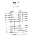
- FIG. 1is a diagram illustrating a program method using a self-boosting scheme according to the prior art.
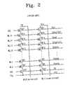
- FIG. 2is a diagram illustrating a program method using a local self-boosting scheme according to the prior art.
- FIG. 3illustrates a floating gate interference model between a selected memory cell transistor and adjacent memory cell transistors thereof, based on capacitive coupling.
- FIG. 4is a block diagram illustrating non-volatile semiconductor memory devices according to embodiments of the present invention.
- FIG. 5illustrates word line voltage conditions of program operations according to embodiments of the present invention.
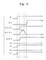
- FIG. 6is a timing diagram illustrating program methods according to embodiments of the present invention.
- FIG. 7illustrates voltage variations of floating gates of adjacent memory cell transistors at a program operation according to embodiments of the present invention.
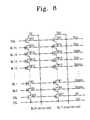
- FIG. 8illustrates word line voltage conditions of program operations according to embodiments of the present invention.
- FIG. 9is a timing diagram illustrating program methods according to embodiments of the present invention.
- a NAND-type flash memorymay include a memory cell array 110 including a plurality of cell strings ST connected to a plurality of bit lines BL 0 -BLm, respectively.
- Each string STincludes a string select transistor SST as a first select transistor, a ground select transistor GST as a second select transistor, and a plurality of, for example, 16 memory cells MC 0 -MC 15 connected in series between the string and ground select transistors SST and GST.
- a string select transistor SST in each stringmay have a drain connected to a corresponding bit line and a gate connected to a string select line.
- a ground select transistor GST in each stringmay have a source connected to a common select line and a gate connected to a ground select line.
- Memory cells MC 0 -MC 15 in each stringmay be connected in series between a source of the string select transistor SST and a drain of the ground select transistor GST.
- Memory cells MC 0 -MC 15 in each stringmay be connected to corresponding word lines WL0-WL15, respectively.
- memory cellsmay be single-bit cells for storing 1-bit of data.
- memory cellsmay be multi-bit cells for storing n-bits of data.
- the bit lines BL 0 -BLmmay be connected to a sense and latch circuit (also referred to as a page buffer circuit) 160 .
- the sense and latch circuit 160charges bit lines according to data bits to be programmed during a program operation.
- the sense and latch circuit 160latches data bits supplied from the outside and supplies 0V or a power supply voltage V cc to bit lines based on the latched data bits.
- the sense and latch circuit 160may supply the power supply voltage V cc to a bit line of a program-inhibit memory cell transistor, so that a channel of the program-inhibit memory cell transistor may be charged up to V cc -V th (V th being a threshold voltage of a string select transistor).
- the sense and latch circuit 160supplies 0V to a bit line of a program memory cell transistor, so that a channel of the program memory cell transistor may be charged to 0V. Supplying of voltages to bit lines can be performed before word line voltages (i.e. program and pass voltages) are applied to corresponding word lines, respectively.
- word line voltagesi.e. program and pass voltages
- the memory device 100may further comprise a switch circuit 120 including a plurality of pass transistors PT 17 -PT 0 connected to a string select line SSL, word lines WL15-WL0, and a ground select line GSL, respectively.
- the pass transistors PT 0 -PT 17can be turned on or off using a common control signal GWL from a first decoder circuit 130 .
- the control signal GWLmay have a voltage sufficient to transfer a word line voltage such as a program voltage V pgm , a pass voltage V pass , a read voltage V read and/or a coupling voltage V cp through the respective pass transistors.
- the string select line SSL, the word lines WL15-WL0 and the ground select line GSLcan be connected to a second decoder circuit 140 through the switch circuit 120 .
- the second decoder circuit 140may select one of the word lines WL0-WL15 in response to row address information, and may be provided with word lines voltages (e.g., V pgm , V pass , V cp and V read ) from a voltage generator circuit 150 .
- the voltage generator circuit 150may include a program voltage generator 151 for generating the program voltage V pgm , a pass voltage generator 152 for generating the pass voltage V pass , a coupling voltage generator 153 for generating the coupling voltage V cp , and a read voltage generator 154 for generating the read voltage V read .
- the voltage generators 151 - 154can be realized using one or more high voltage pumps.
- the switch circuit 120 , the first decoder 130 , and the second decoder circuit 140may provide a row selection circuit. Before a program voltage V pgm is applied to a selected word line (or a first word line) during a program operation, the row selector circuit may apply a coupling voltage V cp to at least one unselected word line (or a second word line) closely adjacent to the first word line, a decoupling voltage V dcp to a word line (or a third word line) closely adjacent to the second word line, and a pass voltage V pass to remaining word lines.
- the decoupling voltage V dcpcan be lower than the coupling and pass voltages V cp and V pass , and the coupling voltage V cp can be lower or higher than the decoupling voltage V dcp .
- the coupling voltage V cpcan be the same as the pass voltage V pass .
- a word line WL15When a word line WL15 is selected, for example, a word line WL14 can be provided with the coupling voltage V cp , a word line WL13 can be provided with the decoupling voltage V dcp , and remaining word lines WL0-WL12 can be provided with the pass voltage V pass .
- a word line WL0when a word line WL0 is selected, a word line WL1 can be provided with the coupling voltage V cp , a word line WL2 can be provided with the decoupling voltage V dcp , and remaining word lines WL3-WL15 can be provided with the pass voltage V pass .
- word lines WL13 and WL15can be provided with the coupling voltage V cp
- a word line WL12can be provided with the decoupling voltage V dcp
- remaining word lines WL0-WL11can be provided with the pass voltage V pass .
- word lines WL0 and WL2can be provided with the coupling voltage V cp
- word lines WL3can be provided with the decoupling voltage V dcp
- remaining word lines WL4-WL15can be provided with the pass voltage V pass .
- the coupling voltage V cpcan be applied to word lines WL12 and WL14 closely adjacent to the selected word line WL13, the decoupling voltage V dcp can be applied to word lines WL11 and WL15 each adjacent to the word lines WL12 and WL14, and the pass voltage V pass can be applied to remaining word lines WL0-WL10.
- a floating gate voltage of a program cell transistor of the selected word linemay become higher than 0V, based on a floating gate voltage(s) of an adjacent cell transistor(s) supplied with a coupling voltage V cp .
- V pgmWhen the program voltage V pgm is applied to the selected word line, an electric field across a tunnel oxide of a program cell transistor connected to the selected word line may thus be relatively increased as compared with a local self-boosting method.
- FIG. 5is a diagram illustrating a word line voltage condition according to a local self-boosting scheme according to embodiments of the present invention.
- FIG. 6is a timing diagram illustrating a program method for a local self-boosting scheme according to embodiments of the present invention.
- a program operation of a NAND-type flash memory according to embodiments of the present inventionwill be described below with reference to FIGS. 5 and 6.
- a bit line connected to a memory cell to be programmedis referred to as a selected bit line
- a bit line connected to a memory cell to be program-inhibitedis referred to as an unselected bit line.
- a word line connected to a memory cell to be programmedis referred to as a selected word line, and remaining word lines are referred to as unselected word lines.
- a term “the most adjacent word line” or “an adjacent word line”means that there are no word lines between two referenced word lines.
- a ground voltage of 0Vis applied to a selected bit line (e.g., BL0) and a power supply voltage V cc is applied to an unselected bit line (e.g., BL1).
- the power supply voltage V ccis applied to a string select line SSL and the ground voltage is applied to a ground select line GSL.
- the power supply voltage or the ground voltageis applied to a common source line CSL.
- a coupling voltage V cpis applied to unselected word lines (e.g., WL12 and WL14) closely adjacent to a selected word line (e.g., WL13), and a pass voltage V pass is applied to remaining word lines (e.g., WL0-WL11, WL15).
- OVinstead of the pass voltage V pass , can be applied to word lines WL11 and WL15 each adjacent to the word lines WL12 and WL14 opposite the selected word line WL13.
- V ccSince the power supply voltage V cc is applied to the string select line SSL, a source of a string select transistor SST connected to the unselected bit line BL1 can be charged up to V cc -V th (V th being a threshold voltage of the string select transistor). A channel of a cell transistor to be program-inhibited can thus be charged up to V cc -V th , and a string select transistor SST connected to the unselected bit line BL1 may be shut off.
- voltages applied to unselected word lines WL11 and WL15may be changed from V pass , to V dcp .
- V pgmis applied to the selected word line WL13.
- the coupling voltage V cpis thus applied to unselected word lines WL12 and WL14 closely adjacent to the selected word line WL13, and the decoupling voltage V dcp is applied to unselected word lines WL11 and WL15 each adjacent to the word lines WL12 and WL14 opposite the selected wordline WL13.
- Remaining word lines WL0-WL15can be provided with the pass voltage V pass (e.g., 10V).
- V passe.g. 10V
- V fg⁇ ONO V pgm ( WL 13)+ ⁇ ONO ⁇ fg V cp ( WL 12)+ ⁇ ONO ⁇ fg V cp ( WL 14).
- V cp (WL12) and V cp (WL14)may be higher than 0V and lower than a pass voltage V pass .
- a voltagemay be induced on a floating gate of a memory cell transistor to be programmed before the program voltage V pgm is applied to the selected word line WL13.
- the voltage induced on the floating gatemay be expressed as follows:
- V fg⁇ ONO ⁇ fg V cp ( WL 12)+ ⁇ ONO ⁇ fg V cp ( WL 14).
- a floating gate voltage of a memory cell to be programmedcan be 0V before a program voltage V pgm is applied.
- a predetermined voltagecan be induced on a floating gate of the memory cell transistor to be programmed before a program voltage V pgm is applied.
- the program voltage V pgmis applied to the selected word line WL13, a higher voltage than that of FIG. 2 can be induced on the floating gate of the memory cell transistor being programmed.
- an electric field across a tunnel oxide of the memory cell transistor to be programmedcan be increased.
- a floating gate voltage of a cell transistor to be programmedcan be determined by a coupling voltage V cp , as shown in FIG. 7.
- a graph in FIG. 7can be obtained using the aforementioned ISSP scheme under the conditions that a spacer of a cell transistor is formed of an SiN material, that its gate-to-gate space and gate length are 0.12 ⁇ m, and that a polysilicon height is 1200 ⁇ .
- an X-axisindicates a program number and a Y-axis indicates a threshold voltage of a cell transistor to be programmed.
- a program numbermay be reduced.
- a memory cellmay be assumed to be programmed to have a threshold voltage of 2V.
- the coupling voltage V cpis 10V
- program cycles or loopsmay be carried out 11 times
- the coupling voltage V cpis 0V
- program cycles or loopsmay be carried out 14 times.
- program methodsmay enable a program cycle to be shortened by three cycles.
- a program speed of a flash memorymay be improved using local self-boosting schemes according to embodiments of the present invention.
- the narrower a gate intervalthe faster the program speed. This result may be provided because a capacitive coupling effect may be strengthened.
- FIG. 8is a diagram illustrating word line voltage conditions according to program methods according to embodiments of the present invention.
- FIG. 9is a timing diagram illustrating program methods according to embodiments of the present invention.
- a coupling voltage V cpcan be applied to unselected word lines WL12 and WL14 closely adjacent to a selected word line WL13, and a pass voltage V pass can be applied to remaining word lines WL0-WL11.
- a coupling effect of a floating gate of a cell transistor to be programmedcan be improved by establishing a relatively high coupling voltage V cp . Improvement of coupling effects may provide improvement of program speeds.
- Self-boosting methods according to embodiments of the present inventioncan be applied to program both single-level cells and/or a multi-level cells.
- a multi-level cellwhich may need a higher program voltage than a single-level cell, it may be possible to program memory cells faster using local self-boosting methods according to embodiments of the present invention. Therefore, local self-boosting methods according to embodiments of the present invention may make it easier to realize a relatively high-speed multi-level memory device without a burdensome increase in a peripheral circuit area.
- a program voltagemay be established differently at program steps of 01, 10 and 00, while a coupling voltage V cp is maintained at each program step.
- Programming of multi-level cellsis discussed for example, in U.S. Pat. No. 5,768,188 entitled “MULTI-STATE NON-VOLATILE SEMICONDUCTOR MEMORY AND METHOD FOR DRIVING THE SAME”, the disclosure of which herein incorporated by reference. A farther discussion of multi-level programming using local self-boosting schemes according to embodiments of the present invention is thus omitted.
- a voltage induced to a floating gate of a cell transistor to be programmedcan be increased by applying a coupling voltage to unselected cell transistors adjacent to the cell transistor to be programmed and by applying a decoupling voltage to cell transistors adjacent to unselected memory cell transistors.
- a time to program memory cellscan thus be shortened.
- a program speed of a non-volatile memory device according to embodiments of the present inventioncan thus be improved.
- Non-volatile semiconductor memoriesmay provide improved program speeds.
- a NAND-type flash memorymay provide an improved local self-boosting scheme where before a program voltage is applied to a selected word line, a coupling voltage (being higher or lower than a pass voltage) is applied to an unselected word line(s) closely adjacent to a selected word line, and a decoupling voltage (e.g., 0V) is applied to an unselected word line(s) adjacent to the unselected word line(s) which is closely adjacent to the selected word line.
- a floating gate voltage of a memory cell transistor connected to the selected word linemay be affected by a floating gate voltage of a memory cell transistor(s) supplied with the coupling voltage.
- an electric field across a tunnel oxide of a memory cell transistor connected to a selected word linecan be increased as compared with a conventional local self-boosting method.
- a program operationmay be performed more rapidly than a conventional local self-boosting method while maintaining an increased channel voltage of a program-inhibit cell transistor.
- a program speedmay be improved by using local self-boosting methods according to embodiments of the present invention.
Landscapes
- Engineering & Computer Science (AREA)
- Microelectronics & Electronic Packaging (AREA)
- Computer Hardware Design (AREA)
- Read Only Memory (AREA)
Abstract
Description
- This application claims the benefit of priority from Korean Patent Application No. 2002-64767, filed on Oct. 23, 2002, the disclosure of which is herein incorporated by reference in its entirety.[0001]
- The present invention relates to semiconductor memory devices, and, more particularly, to methods of programming non-volatile semiconductor memories and related devices.[0002]
- There has been an increasing demand for electrically erasable and programmable memory devices that do not require refreshing of data stored therein. Current trends of memory devices have been to increase capacity and reliability. A NAND-type flash memory is an example of a non-volatile semiconductor memory device that provides relatively large capacity and relatively high reliability without refreshing stored data. Because data can be maintained without power, flash memory devices have been widely applied to battery powered electronic devices (e.g., hand-held terminals and computers, etc.) where power may be interrupted suddenly.[0003]
- A NAND-type flash memory may include electrically erasable and programmable read-only memory cells called “flash EEPROM cells”. Commonly, a flash EEPROM cell may include a memory cell transistor or a floating gate transistor, which may be formed on a pocket P-well region of a substrate and may have spaced apart N-type source and drain regions, a floating gate formed over a channel region between the source and drain regions to store charge, and a control gate placed over the floating gate.[0004]
- A NAND-type flash memory may include a memory cell array, having a plurality of strings (called cell strings or NAND strings) corresponding to bit lines, respectively. Each cell string may include a string select transistor as a first select transistor, a ground select transistor as a second select transistor, and plural memory cells connected in series between the string and ground select transistors. A string select transistor in each string may have a drain connected to a corresponding bit line and a gate connected to a string select line. Aground select transistor in each string may have a source connected to a common select line and a gate connected to a ground select line. Memory cells in each string may be connected in series between a source of the string select transistor and a drain of the ground select transistor. Memory cells in each string may be connected to corresponding word lines, respectively.[0005]
- Initially, for example, memory cells can be erased to have a threshold voltage of −3V. A threshold voltage of a selected memory cell may be shifted to a higher voltage range by applying a relatively high voltage (or a program voltage) (e.g., 20V) to a word line of the selected memory cell at a predetermined time. Threshold voltages of remaining or unselected memory cells are not significantly varied.[0006]
- One problem may arise when programming a portion of memory cells (hereinafter, referred to as “program memory cells”) in a selected word line and program-inhibiting remaining memory cells (hereinafter, referred to as “program-inhibit memory cells”) in the selected word line. When a program voltage is applied to a selected word line, it may be applied to program memory cells and to program-inhibit memory cells at the same time. Program-inhibit memory cells in the selected word line may be programmed according to a phenomenon referred to as “program disturbance”.[0007]
- One method for reducing the program disturbance is a program inhibition method using a self-boosting scheme. Program inhibition methods using self-boosting schemes are discussed, for example, in U.S. Pat. No. 5,677,873 entitled “METHODS OF PROGRAMMING FLASH EEPROM INTEGRATED CIRCUIT MEMORY DEVICES TO PREVENT INADVERTENT PROGRAMMING OF NONDESIGNATED NAND MEMORY CELLS THEREIN” and in U.S. Pat. No. 5,991,202 entitled “METHOD FOR REDUCING PROGRAM DISTURB DURING SELF-BOOSTING IN A NAND FLASH MEMORY”. The disclosures of both of these patents are herein incorporated by reference.[0008]
- A program inhibition method using such a self-boosting scheme will be described below with reference to FIG. 1. A ground path may be formed by applying a voltage of 0V to a gate of a ground select transistor GST. A voltage of 0V may be applied to a selected bit line (e.g., BL0) and a power supply voltage Vcc (as a program inhibition voltage) may be applied to an unselected bit line (e.g., BL1). Simultaneously, a power supply voltage V[0009]ccmay be applied to a string select line SSL. A source of a string select transistor SST connected to the unselected bit line BL1 may be charged up to Vcc-Vth(Vthbeing a threshold voltage of the string select transistor), and then the transistor SST connected to the unselected bit line BL1 may be shut off. A program voltage Vpgmcan be applied to a selected word line (e.g., WL14) and a pass voltage Vpasscan be applied to unselected word lines (e.g., WL0-WL13, WL15), and a channel voltage of a program-inhibit cell transistor can be boosted by the program voltage Vpgm. The boosted channel voltage may be expressed by the following equation:

- In this equation, N is a word line number, V[0010]this a threshold voltage of a string select transistor, Cchis a channel capacitance of a program-inhibit cell transistor, and Ctis a total capacitance of the program-inhibit cell transistor. The Ctis (Cono||Ctun) wherein Cono and Ctun are coupling capacitances.
- Although a program voltage is applied to a control gate of a program-inhibit cell transistor, a boosted channel voltage may reduce F-N tunneling between a floating gate and a channel of the program-inhibit cell transistor. Accordingly, the program-inhibit cell transistor may maintain an initial erased state.[0011]
- Another program-inhibit method using a local self-boosting scheme is discussed, for example, in U.S. Pat. No. 5,715,194 entitled “BIAS SCHEME OF PROGRAM INHIBIT FOR RANDOM PROGRAMMING IN A NAND FLASH MEMORY” and in U.S. Pat. No. 6,061,270 entitled “METHOD FOR PROGRAMMING A NON-VOLATILE MEMORY DEVICE WITH PROGRAM DISTURB CONTROL”. The disclosures of both of these patents are herein incorporated by reference.[0012]
- A program inhibition method using such a local self-boosting scheme will be described below with reference to FIG. 2. A voltage of 0V can be applied to a selected bit line (e.g., BL0), and a power supply voltage V[0013]cc(as a program inhibition voltage) can be applied to an unselected bit line (e.g., BL1). Since a power supply voltage is applied to a string select line SSL, a source of a string select transistor SST connected to the unselected bit line BL1 may be charged up to Vcc-Vth(where Vthis a threshold voltage of the string select transistor). The transistor SST connected to the unselected bit line BL1 can than be shut off.
- A decoupling voltage V[0014]dcpof 0V can be applied to unselected word lines (e.g., WL13 and WL15) closely adjacent to a selected word line (e.g., WL14). A pass voltage Vpass(e.g., 10V) can be applied to remaining word lines (e.g., WL0-WL12). The selected word line can then be supplied with a program voltage Vpgm. With this bias condition, since a channel of a program-inhibit cell transistor may be limited by cell transistors of unselected word lines supplied with a decoupling voltage, a boosted channel voltage of the program-inhibit cell transistor can be higher than that caused by the above self-boosting scheme. Similar to the self-boosting method, the boosted channel voltage may reduce F-N tunneling between a floating gate and a channel of a program-inhibit cell transistor so that the program-inhibit cell transistor can maintain an initial erase state.
- Methods using the local self-boosting scheme may obtain a higher channel voltage than the self-boosting scheme and may thus be used to program a multi-level cell that stores n-bits of data (where n is an integer greater than or equal to 2). However, the local self-boosting scheme may have a lower program speed as compared with the self-boosting scheme.[0015]
- In general, a voltage of a floating gate of a memory cell transistor to be programmed may be affected by voltages of floating gates of adjacent cell transistors through capacitive coupling. Such a phenomenon is discussed, for example, in the IEEE ELECTRON DEVICE LETTERS, VOL.23, NO.5, pp. 264 to 266, May 2002 under the title of “EFFECTS OF FLOATING-GATE INTERFERENCE ON NAND FLASH MEMORY CELL OPERATION.” The disclosure of this reference is incorporated herein by reference. At any memory cell transistor (hereinafter called “reference memory cell transistor”), as shown in FIG. 3, coupling capacitances C[0016]ono, Cfgand Ctunmay exist between a floating gate and a channel (bulk or body) of the reference memory cell transistor and between the floating gate of the reference memory cell transistor and floating gates of adjacent memory cell transistors, respectively. A voltage of a floating gate of the reference memory cell transistor may be affected by the coupling capacitances.
- In this equation, C[0018]onois a control gate-to-floating gate capacitance, Ctunis a floating gate-to-channel capacitance, and Cfgis a floating gate-to-floating gate capacitance.
- In this equation, V[0020]cg1is a voltage applied to a control gate, that is, a voltage applied to an unselected word line.
- In this equation, V[0022]cg2is a voltage applied to a control gate, that is, a voltage applied to an unselected word line.
- Accordingly a voltage V[0023]fgof a floating gate of a reference memory cell transistor may be determined as follows:
- Vfg=γONOVcg+γONOγfgVcg1+γONOγfgVcg2.
- With the local self-boosting method, a program voltage V[0024]pgmmay be applied to a selected word line (e.g., WL14), while a decoupling voltage Vdcpmay be applied to two unselected word lines WL13 and WL15 closely adjacent to the selected word line WL14. Based on this bias condition, a voltage of a floating gate of the reference memory cell transistor may be expressed as follows:
- Vfg=γONOVpgm(WL14)+γONOγfgVdcp(WL13)+γONOγfgVdcp(WL15).
- Since word lines WL13 and WL15 adjacent to a selected word line WL14 are supplied with 0V, values of γ[0025]ONOγfgVdcp(WL13) and γONOγfgVdcp(WL15) become 0V. Therefore, the floating gate voltage Vfgof the reference memory cell transistor may become a voltage of γONOγfgVdcp(WL13).
- In accordance with the above description, since a floating gate voltage V[0026]fgof a reference memory cell transistor may be unaffected by voltages V1 and V2 of floating gates placed at both sides of the floating gate of a reference memory cell transistor, a program speed of a local self-boosting method may be slower than that of a self-boosting method. That is, in the case of the self-boosting method where a pass voltage is applied to unselected word lines, a floating gate voltage of a reference voltage may be increased by capacitive coupling, so that a program speed is increased as compared with the local self-boosting method.
- In case of a NAND flash memory which performs a program operation using an “incremental step pulse programming (ISPP) scheme”, a program voltage V[0027]pgm, for example, can be stepwise increased from 14.7V to 20V as a program cycle is repeated. If a program speed is reduced, a number of program cycles may increase. When using an ISSP scheme, an increase in the program cycle number may require a higher program voltage. This may increase a peripheral circuit (in particular, a high voltage pump) area and a program time. Increases in the peripheral circuit area may result in an increase in a number of high voltage pumping stages used to generate higher voltages.
- According to embodiments of the present invention, methods may be provided for programming a non-volatile memory device including a string of serially connected memory cell transistors with each memory cell transistor of the string being connected to a different word line. In particular, a pass voltage may be applied to a first word line connected to a first memory cell transistor of the string, and a coupling voltage may be applied to a second word line connected to a second memory cell transistor of the string wherein the coupling voltage is greater than a ground voltage of the memory device and wherein the pass voltage and the coupling voltage are different. In addition, a program voltage may be applied to a third word line connected to a third memory cell transistor of the string while applying the pass voltage to the first word line and while applying the coupling voltage to the second word line, with the third memory cell transistor being programmed responsive to applying the program voltage to the third word line. More particularly, the second memory cell transistor may be between the first and third memory cell transistors of the serially connected string.[0028]
- The pass voltage may also be applied to a fourth word line connected to a fourth memory cell transistor of the string wherein the first memory cell transistor is serially connected between the fourth memory cell transistor and the second memory cell transistor, and the coupling voltage can be greater than the pass voltage. In one alternative, each memory cell transistor of the string can store one bit of data, and in another alternative, each memory cell of the transistor of the string can store a plurality of bits of data.[0029]
- In addition, a decoupling voltage can be applied to a fourth word line connected to a fourth memory cell transistor of the string wherein the fourth memory cell transistor of the string is serially connected between the first and second memory cell transistors. More particularly, the decoupling voltage can be less than the pass voltage, less than the coupling voltage, and less than the program voltage, and the program voltage can be applied to the third word line while applying the pass voltage to the first word line, while applying the coupling voltage to the second word line, and while applying the decoupling voltage to the fourth word line. The decoupling voltage may be a ground voltage of the memory device, or the decoupling voltage can be less than a ground voltage of the memory device. Before applying the decoupling voltage to the fourth word line, a preliminary voltage can be applied to the fourth word line wherein the preliminary voltage is greater than the decoupling voltage and wherein the decoupling voltage is applied to the fourth word line before applying the program voltage to the third word line. Moreover, the preliminary voltage can be equal to the pass voltage.[0030]
- The non-volatile memory device may also include a second string of serially connected memory cell transistors with a memory cell transistor of the second string being connected to the third word line. With the second string of memory cell transistors, a channel of the third memory cell transistor may be precharged with a first precharge voltage before applying the program voltage, and a channel of the memory cell transistor of the second string connected to the third word line may be precharged with a second voltage different than the first voltage before applying the program voltage. Moreover, the first voltage may be a ground voltage of the memory device, and the second voltage may be a difference between a power supply voltage of the memory device and a threshold voltage of the select transistor of the second string.[0031]
- According to additional embodiments of the present invention, methods may be provided for programming a non-volatile memory device including a string of serially connected memory cell transistors with each memory cell transistor of the string being connected to a different word line. In particular, a decoupling voltage may be applied to a first word line connected to a first memory cell transistor of the string, and a coupling voltage may be applied to a second word line connected to a second memory cell transistor of the string wherein the coupling voltage is greater than the decoupling voltage. In addition, a program voltage can be applied to a third word line connected to a third memory cell transistor of the string while applying the decoupling voltage to the first word line and while applying the coupling voltage to the second word line. More particularly, the third memory cell transistor may be programmed responsive to applying the program voltage to the third word line, and the second memory cell transistor may be between the first and third memory cell transistors of the serially connected string.[0032]
- Before applying the decoupling voltage to the first word line, a preliminary voltage may be applied to the first word line wherein the preliminary voltage is greater that the decoupling voltage and wherein the decoupling voltage is applied to the first word line before applying the program voltage to the third word line. In addition, a pass voltage may be applied to a fourth word line connected to a fourth memory cell transistor of the string wherein the first memory cell transistor is serially connected between the fourth and second memory cell transistors, and the pass voltage may be greater than the decoupling voltage, and/or the pass voltage may be equal to the preliminary voltage.[0033]
- A pass voltage may also be applied to a fourth word line connected to a fourth memory cell transistor of the string wherein the first memory cell transistor is serially connected between the fourth and second memory cell transistors, and the pass voltage may be greater than the decoupling voltage. In addition, the pass voltage may be applied to a fifth word line connected to a fifth memory cell transistor of the string wherein the fourth memory cell transistor is serially connected between the fifth and first memory cell transistors. More particularly, the coupling voltage may be greater than or equal to the pass voltage, or the coupling voltage may be greater than the pass voltage.[0034]
- Each memory cell of the string may store one bit of date, or each memory cell of the string may store a plurality of bits of data. Moreover, the decoupling voltage may be a ground voltage of the memory device, or the decoupling voltage may be less than a ground voltage of the memory device. The non-volatile memory device may also include a second string of serially connected memory cell transistors with a memory cell transistor of the second string being connected to the third word line. With the second string of memory cell transistors, a channel of the third memory cell transistor may be precharged with a first precharge voltage before applying the program voltage, and a channel of the memory cell transistor of the second string connected to the third word line may be precharged with a second voltage different than the first voltage before applying the program voltage. More particularly, the first voltage may be a ground voltage of the memory device, and the second voltage may be a difference between a power supply voltage of the memory device and a threshold voltage of the select transistor of the second string.[0035]
- According to still additional embodiments of the present invention, a non-volatile memory device may include a string of serially connected memory cell transistors, a plurality of word lines with each word line being connected to a different one of the serially connected memory cell transistors, and a row selection circuit connected to the plurality of word lines. The row selection circuit may be configured to apply a pass voltage to a first word line connected to a first memory cell transistor of the string and to apply a coupling voltage to a second word line connected to a second memory cell transistor of the string wherein the coupling voltage is greater than a ground voltage of the memory device and wherein the pass voltage and the coupling voltage are different. The row selection circuit may also be configured to apply a program voltage to a third word line connected to a third memory cell transistor of the string while applying the pass voltage to the first word line and while applying the coupling voltage to the second word line with the third memory cell transistor being programmed responsive to applying the program voltage to the third word line. In addition, the second memory cell transistor may be between the first and third memory cell transistors of the serially connected string.[0036]
- According to yet additional embodiments of the present invention, a non-volatile memory device may include a string of serially connected memory cell transistors, a plurality of word lines with each word line being connected to a different one of the serially connected memory cell transistors, and a row selection circuit connected to the plurality of word lines. The row selection circuit may be configured to apply a decoupling voltage to a first word line connected to a first memory cell transistor of the string, and to apply a coupling voltage to a second word line connected to a second memory cell transistor of the string wherein the coupling voltage is greater than the decoupling voltage. The row selection circuit may also be configured to apply a program voltage to a third word line connected to a third memory cell transistor of the string while applying the decoupling voltage to the first word line and while applying the coupling voltage to the second word line with the third memory cell transistor being programmed responsive to applying the program voltage to the third word line. In addition, the second memory cell transistor may be between the first and third memory cell transistors of the serially connected string.[0037]
- FIG. 1 is a diagram illustrating a program method using a self-boosting scheme according to the prior art.[0038]
- FIG. 2 is a diagram illustrating a program method using a local self-boosting scheme according to the prior art.[0039]
- FIG. 3 illustrates a floating gate interference model between a selected memory cell transistor and adjacent memory cell transistors thereof, based on capacitive coupling.[0040]
- FIG. 4 is a block diagram illustrating non-volatile semiconductor memory devices according to embodiments of the present invention.[0041]
- FIG. 5 illustrates word line voltage conditions of program operations according to embodiments of the present invention.[0042]
- FIG. 6 is a timing diagram illustrating program methods according to embodiments of the present invention.[0043]
- FIG. 7 illustrates voltage variations of floating gates of adjacent memory cell transistors at a program operation according to embodiments of the present invention.[0044]
- FIG. 8 illustrates word line voltage conditions of program operations according to embodiments of the present invention.[0045]
- FIG. 9 is a timing diagram illustrating program methods according to embodiments of the present invention.[0046]
- The present invention will be described more fully hereinafter with reference to the accompanying drawings, in which typical embodiments of the invention are shown. This invention, however, may be embodied in many different forms and should not be construed as limited to the embodiments set forth herein. Rather, these embodiments are provided so that this disclosure will be thorough and complete, and will fully convey the scope of the invention to those skilled in the art. It will also be understood that when an element is referred to as being “coupled” or “connected” to another element, it can be directly coupled or connected to the other element or intervening elements may also be present. In contrast, when an element is referred to as being “directly coupled” or “directly connected” to another element, there are no intervening elements present. Like numbers refer to like elements throughout.[0047]
- Referring to FIG. 4, a NAND-type flash memory according to embodiments of the present invention may include a[0048]
memory cell array 110 including a plurality of cell strings ST connected to a plurality of bit lines BL0-BLm, respectively. Each string ST includes a string select transistor SST as a first select transistor, a ground select transistor GST as a second select transistor, and a plurality of, for example, 16 memory cells MC0-MC15 connected in series between the string and ground select transistors SST and GST. A string select transistor SST in each string may have a drain connected to a corresponding bit line and a gate connected to a string select line. A ground select transistor GST in each string may have a source connected to a common select line and a gate connected to a ground select line. Memory cells MC0-MC15 in each string may be connected in series between a source of the string select transistor SST and a drain of the ground select transistor GST. Memory cells MC0-MC15 in each string may be connected to corresponding word lines WL0-WL15, respectively. - In memories according to embodiments of the present invention, memory cells may be single-bit cells for storing 1-bit of data. Alternatively, memory cells may be multi-bit cells for storing n-bits of data.[0049]
- The bit lines BL[0050]0-BLm may be connected to a sense and latch circuit (also referred to as a page buffer circuit)160. The sense and
latch circuit 160 charges bit lines according to data bits to be programmed during a program operation. At the program operation, the sense andlatch circuit 160 latches data bits supplied from the outside andsupplies 0V or a power supply voltage Vccto bit lines based on the latched data bits. For example, the sense andlatch circuit 160 may supply the power supply voltage Vccto a bit line of a program-inhibit memory cell transistor, so that a channel of the program-inhibit memory cell transistor may be charged up to Vcc-Vth(Vthbeing a threshold voltage of a string select transistor). The sense andlatch circuit 160supplies 0V to a bit line of a program memory cell transistor, so that a channel of the program memory cell transistor may be charged to 0V. Supplying of voltages to bit lines can be performed before word line voltages (i.e. program and pass voltages) are applied to corresponding word lines, respectively. - The[0051]
memory device 100 may further comprise aswitch circuit 120 including a plurality of pass transistors PT17-PT0 connected to a string select line SSL, word lines WL15-WL0, and a ground select line GSL, respectively. The pass transistors PT0-PT17 can be turned on or off using a common control signal GWL from afirst decoder circuit 130. The control signal GWL may have a voltage sufficient to transfer a word line voltage such as a program voltage Vpgm, a pass voltage Vpass, a read voltage Vreadand/or a coupling voltage Vcpthrough the respective pass transistors. The string select line SSL, the word lines WL15-WL0 and the ground select line GSL can be connected to asecond decoder circuit 140 through theswitch circuit 120. Thesecond decoder circuit 140 may select one of the word lines WL0-WL15 in response to row address information, and may be provided with word lines voltages (e.g., Vpgm, Vpass, Vcpand Vread) from avoltage generator circuit 150. Thevoltage generator circuit 150 may include aprogram voltage generator 151 for generating the program voltage Vpgm, apass voltage generator 152 for generating the pass voltage Vpass, acoupling voltage generator 153 for generating the coupling voltage Vcp, and aread voltage generator 154 for generating the read voltage Vread. The voltage generators151-154 can be realized using one or more high voltage pumps. - The[0052]
switch circuit 120, thefirst decoder 130, and thesecond decoder circuit 140 may provide a row selection circuit. Before a program voltage Vpgmis applied to a selected word line (or a first word line) during a program operation, the row selector circuit may apply a coupling voltage Vcpto at least one unselected word line (or a second word line) closely adjacent to the first word line, a decoupling voltage Vdcpto a word line (or a third word line) closely adjacent to the second word line, and a pass voltage Vpassto remaining word lines. The decoupling voltage Vdcpcan be lower than the coupling and pass voltages Vcpand Vpass, and the coupling voltage Vcpcan be lower or higher than the decoupling voltage Vdcp. Alternatively, the coupling voltage Vcpcan be the same as the pass voltage Vpass. - When a word line WL15 is selected, for example, a word line WL14 can be provided with the coupling voltage V[0053]cp, a word line WL13 can be provided with the decoupling voltage Vdcp, and remaining word lines WL0-WL12 can be provided with the pass voltage Vpass. Likewise, when a word line WL0 is selected, a word line WL1 can be provided with the coupling voltage Vcp, a word line WL2 can be provided with the decoupling voltage Vdcp, and remaining word lines WL3-WL15 can be provided with the pass voltage Vpass.
- Alternatively, when a word line WL14 is selected, word lines WL13 and WL15 can be provided with the coupling voltage V[0054]cp, a word line WL12 can be provided with the decoupling voltage Vdcp, and remaining word lines WL0-WL11 can be provided with the pass voltage Vpass. Likewise, when a word line WL1 is selected, word lines WL0 and WL2 can be provided with the coupling voltage Vcp, a word line WL3 can be provided with the decoupling voltage Vdcp, and remaining word lines WL4-WL15 can be provided with the pass voltage Vpass. When one (e.g., WL13) of word lines WL3-WL13 is selected, the coupling voltage Vcpcan be applied to word lines WL12 and WL14 closely adjacent to the selected word line WL13, the decoupling voltage Vdcpcan be applied to word lines WL11 and WL15 each adjacent to the word lines WL12 and WL14, and the pass voltage Vpasscan be applied to remaining word lines WL0-WL10.
- Before a program voltage V[0055]pgmis applied to a selected word line, a floating gate voltage of a program cell transistor of the selected word line may become higher than 0V, based on a floating gate voltage(s) of an adjacent cell transistor(s) supplied with a coupling voltage Vcp. When the program voltage Vpgmis applied to the selected word line, an electric field across a tunnel oxide of a program cell transistor connected to the selected word line may thus be relatively increased as compared with a local self-boosting method.
- FIG. 5 is a diagram illustrating a word line voltage condition according to a local self-boosting scheme according to embodiments of the present invention. FIG. 6 is a timing diagram illustrating a program method for a local self-boosting scheme according to embodiments of the present invention. A program operation of a NAND-type flash memory according to embodiments of the present invention will be described below with reference to FIGS. 5 and 6. Hereinafter, a bit line connected to a memory cell to be programmed is referred to as a selected bit line, and a bit line connected to a memory cell to be program-inhibited is referred to as an unselected bit line. Likewise, a word line connected to a memory cell to be programmed is referred to as a selected word line, and remaining word lines are referred to as unselected word lines. In this specification, a term “the most adjacent word line” or “an adjacent word line” means that there are no word lines between two referenced word lines.[0056]
- At time t1, a ground voltage of 0V is applied to a selected bit line (e.g., BL0) and a power supply voltage V[0057]ccis applied to an unselected bit line (e.g., BL1). The power supply voltage Vccis applied to a string select line SSL and the ground voltage is applied to a ground select line GSL. The power supply voltage or the ground voltage is applied to a common source line CSL. Then, between time t1 and time t2, a coupling voltage Vcpis applied to unselected word lines (e.g., WL12 and WL14) closely adjacent to a selected word line (e.g., WL13), and a pass voltage Vpassis applied to remaining word lines (e.g., WL0-WL11, WL15). Alternatively, as shown in FIG. 6 by a dotted line, OV instead of the pass voltage Vpass, can be applied to word lines WL11 and WL15 each adjacent to the word lines WL12 and WL14 opposite the selected word line WL13.
- Since the power supply voltage V[0058]ccis applied to the string select line SSL, a source of a string select transistor SST connected to the unselected bit line BL1 can be charged up to Vcc-Vth(Vthbeing a threshold voltage of the string select transistor). A channel of a cell transistor to be program-inhibited can thus be charged up to Vcc-Vth, and a string select transistor SST connected to the unselected bit line BL1 may be shut off. At time t2, voltages applied to unselected word lines WL11 and WL15 may be changed from Vpass, to Vdcp. At time t3, a program voltage Vpgmis applied to the selected word line WL13.
- At time t3, the coupling voltage V[0059]cpis thus applied to unselected word lines WL12 and WL14 closely adjacent to the selected word line WL13, and the decoupling voltage Vdcpis applied to unselected word lines WL11 and WL15 each adjacent to the word lines WL12 and WL14 opposite the selected wordline WL13. Remaining word lines WL0-WL15 can be provided with the pass voltage Vpass(e.g., 10V). With this bias condition, before a program voltage Vpgmis applied to the selected word line WL13, a predetermined voltage can be induced to a floating gate of a memory cell transistor to be programmed. The floating gate voltage may be expressed as follows:
- Vfg=γONOVpgm(WL13)+γONOγfgVcp(WL12)+γONOγfgVcp(WL14).
- In this equation V[0060]cp(WL12) and Vcp(WL14) may be higher than 0V and lower than a pass voltage Vpass.
- It should be understood from the above equation that a voltage may be induced on a floating gate of a memory cell transistor to be programmed before the program voltage V[0061]pgmis applied to the selected word line WL13. The voltage induced on the floating gate may be expressed as follows:
- Vfg=γONOγfgVcp(WL12)+γONOγfgVcp(WL14).
- In the case of a local self-boosting method as described with respect to FIG. 2, a floating gate voltage of a memory cell to be programmed can be 0V before a program voltage V[0062]pgmis applied. With local self-boosting methods according to embodiments of the present invention, a predetermined voltage can be induced on a floating gate of the memory cell transistor to be programmed before a program voltage Vpgmis applied. Afterward, when the program voltage Vpgmis applied to the selected word line WL13, a higher voltage than that of FIG. 2 can be induced on the floating gate of the memory cell transistor being programmed. Thus, an electric field across a tunnel oxide of the memory cell transistor to be programmed can be increased. At this time, a channel voltage of a cell transistor to be program-inhibited may be expressed as follows:

- As understood from the above equations, a floating gate voltage of a cell transistor to be programmed can be determined by a coupling voltage V[0063]cp, as shown in FIG. 7. A graph in FIG. 7 can be obtained using the aforementioned ISSP scheme under the conditions that a spacer of a cell transistor is formed of an SiN material, that its gate-to-gate space and gate length are 0.12 μm, and that a polysilicon height is 1200 Å. In FIG. 7, an X-axis indicates a program number and a Y-axis indicates a threshold voltage of a cell transistor to be programmed.
- As shown in FIG. 7, as a coupling voltage V[0064]cpincreases, a program number may be reduced. For example, a memory cell may be assumed to be programmed to have a threshold voltage of 2V. When the coupling voltage Vcpis 10V, program cycles or loops may be carried out 11 times, and when the coupling voltage Vcpis 0V, program cycles or loops may be carried out 14 times. Thus program methods, according to embodiments of the present invention, may enable a program cycle to be shortened by three cycles. A program speed of a flash memory may be improved using local self-boosting schemes according to embodiments of the present invention. In particular, with local self-boosting schemes according to some embodiments of the present invention, the narrower a gate interval, the faster the program speed. This result may be provided because a capacitive coupling effect may be strengthened.
- FIG. 8 is a diagram illustrating word line voltage conditions according to program methods according to embodiments of the present invention. FIG. 9 is a timing diagram illustrating program methods according to embodiments of the present invention. As shown in FIGS. 8 and 9, a coupling voltage V[0065]cpcan be applied to unselected word lines WL12 and WL14 closely adjacent to a selected word line WL13, and a pass voltage Vpasscan be applied to remaining word lines WL0-WL11. Aspects of a program method in FIG. 8 can be similar to aspects of a self-boosting scheme in FIG. I with different bias conditions, and description of similarities is thus omitted. A coupling effect of a floating gate of a cell transistor to be programmed can be improved by establishing a relatively high coupling voltage Vcp. Improvement of coupling effects may provide improvement of program speeds.
- Self-boosting methods according to embodiments of the present invention can be applied to program both single-level cells and/or a multi-level cells. In particular, in the case of a multi-level cell which may need a higher program voltage than a single-level cell, it may be possible to program memory cells faster using local self-boosting methods according to embodiments of the present invention. Therefore, local self-boosting methods according to embodiments of the present invention may make it easier to realize a relatively high-speed multi-level memory device without a burdensome increase in a peripheral circuit area. In the case of a multi-level memory device, when data of 11, 01, 10 and 00 is programmed, a program voltage may be established differently at program steps of 01, 10 and 00, while a coupling voltage V[0066]cpis maintained at each program step. Programming of multi-level cells is discussed for example, in U.S. Pat. No. 5,768,188 entitled “MULTI-STATE NON-VOLATILE SEMICONDUCTOR MEMORY AND METHOD FOR DRIVING THE SAME”, the disclosure of which herein incorporated by reference. A farther discussion of multi-level programming using local self-boosting schemes according to embodiments of the present invention is thus omitted.
- As set forth above, a voltage induced to a floating gate of a cell transistor to be programmed can be increased by applying a coupling voltage to unselected cell transistors adjacent to the cell transistor to be programmed and by applying a decoupling voltage to cell transistors adjacent to unselected memory cell transistors. A time to program memory cells can thus be shortened. A program speed of a non-volatile memory device according to embodiments of the present invention can thus be improved.[0067]
- Non-volatile semiconductor memories according to embodiments of the present invention may provide improved program speeds. A NAND-type flash memory according to embodiments of the present invention may provide an improved local self-boosting scheme where before a program voltage is applied to a selected word line, a coupling voltage (being higher or lower than a pass voltage) is applied to an unselected word line(s) closely adjacent to a selected word line, and a decoupling voltage (e.g., 0V) is applied to an unselected word line(s) adjacent to the unselected word line(s) which is closely adjacent to the selected word line. A floating gate voltage of a memory cell transistor connected to the selected word line may be affected by a floating gate voltage of a memory cell transistor(s) supplied with the coupling voltage. Accordingly, an electric field across a tunnel oxide of a memory cell transistor connected to a selected word line can be increased as compared with a conventional local self-boosting method. As a result, a program operation may be performed more rapidly than a conventional local self-boosting method while maintaining an increased channel voltage of a program-inhibit cell transistor. A program speed may be improved by using local self-boosting methods according to embodiments of the present invention.[0068]
- While this invention has been particularly shown and described with reference to preferred embodiments thereof, it will be understood by those skilled in the art that various changes in form and details may be made therein without departing from the spirit and scope of the invention as defined by the appended claims and their equivalents.[0069]


Claims (80)
1. A method of programming a non-volatile memory device including a string of serially connected memory cell transistors with each memory cell transistor of the string being connected to a different word line, the method comprising:
applying a pass voltage to a first word line connected to a first memory cell transistor of the string;
applying a coupling voltage to a second word line connected to a second memory cell transistor of the string wherein the coupling voltage is greater than a ground voltage of the memory device and wherein the pass voltage and the coupling voltage are different; and
while applying the pass voltage to the first word line and while applying the coupling voltage to the second word line, applying a program voltage to a third word line connected to a third memory cell transistor of the string, the third memory cell transistor being programmed responsive to applying the program voltage to the third word line wherein the second memory cell transistor is between the first and third memory cell transistors of the serially connected string.
2. A method according toclaim 1 further comprising:
applying the pass voltage to a fourth word line connected to a fourth memory cell transistor of the string wherein the first memory cell transistor is serially connected between the fourth memory cell transistor and the second memory cell transistor.
3. A method according toclaim 1 wherein the coupling voltage is greater than the pass voltage.
4. A method according toclaim 1 wherein each memory cell transistor of the string stores one bit of data.
5. A method according toclaim 1 wherein each memory cell of the transistor of the string stores a plurality of bits of data.
6. A method according toclaim 1 further comprising:
applying a decoupling voltage to a fourth word line connected to a fourth memory cell transistor of the string wherein the fourth memory cell transistor of the string is serially connected between the first and second memory cell transistors;
wherein the decoupling voltage is less than the pass voltage, less than the coupling voltage, and less than the program voltage; and
wherein the program voltage is applied to the third word line while applying the pass voltage to the first word line, while applying the coupling voltage to the second word line, and while applying the decoupling voltage to the fourth word line.
7. A method according toclaim 6 wherein the decoupling voltage comprises a ground voltage of the memory device.
8. A method according toclaim 6 wherein the decoupling voltage is less than a ground voltage of the memory device.
9. A method according toclaim 6 further comprising:
before applying the decoupling voltage to the fourth word line, applying a preliminary voltage to the fourth word line wherein the preliminary voltage is greater than the decoupling voltage and wherein the decoupling voltage is applied to the fourth word line before applying the program voltage to the third word line.
10. A method according toclaim 9 wherein the preliminary voltage is equal to the pass voltage.
11. A method according toclaim 1 wherein the non-volatile memory device includes a second string of serially connected memory cell transistors with a memory cell transistor of the second string being connected to the third word line, the method further comprising:
before applying the program voltage, precharging a channel of the third memory cell transistor with a first precharge voltage; and
before applying the program voltage, precharging a channel of the memory cell transistor of the second string connected to the third word line with a second voltage different than the first voltage.
12. A method according toclaim 11 wherein the first voltage is a ground voltage of the memory device and wherein the second voltage is a difference between a power supply voltage of the memory device and a threshold voltage of the select transistor of the second string.
13. A method of programming a non-volatile memory device including string of serially connected memory cell transistors with each memory cell transistor of the string being connected to a different word line, the method comprising:
applying a decoupling voltage to a first word line connected to a first memory cell transistor of the string;
applying a coupling voltage to a second word line connected to a second memory cell transistor of the string wherein the coupling voltage is greater than the decoupling voltage; and
while applying the decoupling voltage to the first word line and while applying the coupling voltage to the second word line, applying a program voltage to a third word line connected to a third memory cell transistor of the string, the third memory cell transistor being programmed responsive to applying the program voltage to the third word line wherein the second memory cell transistor is between the first and third memory cell transistors of the serially connected string.
14. A method according toclaim 13 further comprising:
before applying the decoupling voltage to the first word line, applying a preliminary voltage to the first word line wherein the preliminary voltage is greater that the decoupling voltage and wherein the decoupling voltage is applied to the first word line before applying the program voltage to the third word line.
15. A method according toclaim 14 further comprising:
applying a pass voltage to a fourth word line connected to a fourth memory cell transistor of the string wherein the first memory cell transistor is serially connected between the fourth and second memory cell transistors, wherein the pass voltage is greater than the decoupling voltage, and wherein the pass voltage is equal to the preliminary voltage.
16. A method according toclaim 13 further comprising:
applying a pass voltage to a fourth word line connected to a fourth memory cell transistor of the string wherein the first memory cell transistor is serially connected between the fourth and second memory cell transistors, wherein the pass voltage is greater than the decoupling voltage.
17. A method according toclaim 16 further comprising:
applying the pass voltage to a fifth word line connected to a fifth memory cell transistor of the string wherein the fourth memory cell transistor is serially connected between the fifth and first memory cell transistors.
18. A method according toclaim 16 wherein the coupling voltage is greater than or equal to the pass voltage.
19. A method according toclaim 16 wherein the coupling voltage is greater than the pass voltage.
20. A method according toclaim 13 wherein each memory cell of the string stores one bit of data.
21. A method according toclaim 13 wherein each memory cell of the string stores a plurality of bits of data.
22. A method according toclaim 13 wherein the decoupling voltage comprises a ground voltage of the memory device.
23. A method according toclaim 13 wherein the decoupling voltage is less than a ground voltage of the memory device.
24. A method according toclaim 13 wherein the non-volatile memory device includes a second string of serially connected memory cell transistors with a memory cell transistor of the second string being connected to the third word line, the method further comprising:
before applying the program voltage, precharging a channel of the third memory cell transistor with a first precharge voltage; and
before applying the program voltage, precharging a channel of the memory cell transistor of the second string connected to the third word line with a second voltage different than the first voltage.
25. A method according toclaim 24 wherein the first voltage is a ground voltage of the memory device and wherein the second voltage is a difference between a power supply voltage of the memory device and a threshold voltage of the select transistor of the second string.
26. A non-volatile memory device comprising:
a string of serially connected memory cell transistors
a plurality of word lines with each word line being connected to a different one of the serially connected memory cell transistors; and
a row selection circuit connected to the plurality of word lines, the row selection circuit being configured to apply a pass voltage to a first word line connected to a first memory cell transistor of the string, the row selection circuit being configured to apply a coupling voltage to a second word line connected to a second memory cell transistor of the string wherein the coupling voltage is greater than a ground voltage of the memory device and wherein the pass voltage and the coupling voltage are different, and the row selection circuit being configured to apply a program voltage to a third word line connected to a third memory cell transistor of the string while applying the pass voltage to the first word line and while applying the coupling voltage to the second word line, the third memory cell transistor being programmed responsive to applying the program voltage to the third word line wherein the second memory cell transistor is between the first and third memory cell transistors of the serially connected string.
27. A non-volatile memory device according toclaim 26 wherein the row selection circuit is further configured to apply the pass voltage to a fourth word line connected to a fourth memory cell transistor of the string wherein the first memory cell transistor is serially connected between the fourth memory cell transistor and the second memory cell transistor.
28. A non-volatile memory device according toclaim 26 wherein the coupling voltage is greater than the pass voltage.
29. A non-volatile memory device according toclaim 26 wherein each memory cell transistor of the string stores one bit of data.
30. A non-volatile memory device according toclaim 26 wherein each memory cell of the transistor of the string stores a plurality of bits of data.
31. A non-volatile memory device according toclaim 26 wherein the row selection circuit is further configured to apply a decoupling voltage to a fourth word line connected to a fourth memory cell transistor of the string wherein the fourth memory cell transistor of the string is serially connected between the first and second memory cell transistors, wherein the decoupling voltage is less than the pass voltage, less than the coupling voltage, and less than the program voltage, and wherein the program voltage is applied to the third word line while applying the pass voltage to the first word line, while applying the coupling voltage to the second word line, and while applying the decoupling voltage to the fourth word line.
32. A non-volatile memory device according toclaim 31 wherein the decoupling voltage comprises a ground voltage of the memory device.
33. A non-volatile memory device according toclaim 31 wherein the decoupling voltage is less than a ground voltage of the memory device.
34. A non-volatile memory device according toclaim 31 wherein the row selection circuit is further configured to apply a preliminary voltage to the fourth word line before applying the decoupling voltage to the fourth word line, wherein the preliminary voltage is greater than the decoupling voltage and wherein the decoupling voltage is applied to the fourth word line before applying the program voltage to the third word line.
35. A non-volatile memory device according toclaim 34 wherein the preliminary voltage is equal to the pass voltage.
36. A non-volatile memory device according toclaim 26 further comprising:
a second string of serially connected memory cell transistors with a memory cell transistor of the second string being connected to the third word line; and
a precharge circuit coupled to the first and second strings of serially connected memory cell transistors wherein the precharge circuit is configured to precharge a channel of the third memory cell transistor with a first precharge voltage before applying the program voltage, and wherein the precharge circuit is configured to precharge a channel of the memory cell transistor of the second string connected to the third word line with a second voltage different than the first voltage before applying the program voltage.
37. A non-volatile memory device according toclaim 36 wherein the first voltage is a ground voltage of the memory device and wherein the second voltage is a difference between a power supply voltage of the memory device and a threshold voltage of a select transistor of the second string.
38. A non-volatile memory device comprising:
a string of serially connected memory cell transistors;
a plurality of word lines with each word line being connected to a different one of the serially connected memory cell transistors; and
a row selection circuit connected to the plurality of word lines, the row selection circuit being configured to apply a decoupling voltage to a first word line connected to a first memory cell transistor of the string, the row selection circuit being configured to apply a coupling voltage to a second word line connected to a second memory cell transistor of the string wherein the coupling voltage is greater than the decoupling voltage, and the row selection circuit being configured to apply a program voltage to a third word line connected to a third memory cell transistor of the string while applying the decoupling voltage to the first word line and while applying the coupling voltage to the second word line, the third memory cell transistor being programmed responsive to applying the program voltage to the third word line wherein the second memory cell transistor is between the first and third memory cell transistors of the serially connected string.
39. A non-volatile memory device according toclaim 38 wherein the row selection circuit is further configured to apply a preliminary voltage to the first word line before applying the decoupling voltage to the first word line, wherein the preliminary voltage is greater that the decoupling voltage and wherein the decoupling voltage is applied to the first word line before applying the program voltage to the third word line.
40. A non-volatile memory device according toclaim 39 wherein the row selection circuit is further configured to apply a pass voltage to a fourth word line connected to a fourth memory cell transistor of the string wherein the first memory cell transistor is serially connected between the fourth and second memory cell transistors, wherein the pass voltage is greater than the decoupling voltage, and wherein the pass voltage is equal to the preliminary voltage.
41. A non-volatile memory device according toclaim 38 wherein the row selection circuit is further configured to apply a pass voltage to a fourth word line connected to a fourth memory cell transistor of the string wherein the first memory cell transistor is serially connected between the fourth and second memory cell transistors, wherein the pass voltage is greater than the decoupling voltage.
42. A non-volatile memory device according toclaim 41 wherein the row selection circuit is further configured to apply the pass voltage to a fifth word line connected to a fifth memory cell transistor of the string wherein the fourth memory cell transistor is serially connected between the fifth and first memory cell transistors.
43. A non-volatile memory device according toclaim 41 wherein the coupling voltage is greater than or equal to the pass voltage.
44. A non-volatile memory device according toclaim 41 wherein the coupling voltage is greater than the pass voltage.
45. A non-volatile memory device according toclaim 38 wherein each memory cell of the string stores one bit of data.
46. A non-volatile memory device according toclaim 38 wherein each memory cell of the string stores a plurality of bits of data.
47. A non-volatile memory device according toclaim 38 wherein the decoupling voltage comprises a ground voltage of the memory device.
48. A non-volatile memory device according toclaim 38 wherein the decoupling voltage is less than a ground voltage of the memory device.
49. A non-volatile memory device according toclaim 38 further comprising:
a second string of serially connected memory cell transistors with a memory cell transistor of the second string being connected to the third word line;
a precharge circuit connected to the first and second strings of serially connected memory cells, the precharge circuit being configured to precharge a channel of the third memory cell transistor with a first precharge voltage before applying the program voltage, and the precharge circuit being configured to precharge a channel of the memory cell transistor of the second string connected to the third word line with a second voltage different than the first voltage before applying the program voltage.
50. A non-volatile memory device according toclaim 49 wherein the first voltage is a ground voltage of the memory device and wherein the second voltage is a difference between a power supply voltage of the memory device and a threshold voltage of a select transistor of the second string.
51. A program method of a non-volatile semiconductor memory device which includes strings each connected to corresponding bit lines and each having a plurality of memory cell transistors, the memory cell transistors being connected in series between first and second select transistors and to corresponding word lines, the program method comprising the steps of:
supplying a coupling voltage to at least one first word line and a decoupling voltage to a second word line; and
supplying a program voltage to a third word line connected to a memory cell transistor to be programmed, wherein the first word line is closely adjacent to the third word line and the second word line is closely adjacent word line to the first word line; and wherein the coupling voltage is higher than the decoupling voltage.
52. The program method according toclaim 51 , wherein a pass voltage is supplied to remaining word lines.
53. The program method according toclaim 52 , wherein the coupling voltage is equal to or higher than the pass voltage.
54. The program method according toclaim 53 , further comprising the step of precharging a channel of the memory cell transistor to be programmed with a first voltage and a channel of a memory cell transistor to be program-inhibited with a second voltage.
55. The program method according toclaim 54 , wherein the first voltage is a ground voltage and the second voltage is (Vcc-Vth), the Vth being a threshold voltage of the first select transistor and the Vcc being a power supply voltage.
56. The program method according toclaim 51 , wherein each of the memory cell transistors stores 1-bit data.
57. The program method according toclaim 51 , wherein each of the memory cell transistors stores multi-bit data.
58. The program method according toclaim 51 , wherein the decoupling voltage is a ground voltage.
59. The program method according toclaim 51 , wherein the decoupling voltage is lower than a ground voltage.
60. A program method of a non-volatile semiconductor memory device which includes strings each connected to corresponding bit lines and each having a plurality of memory cell transistors, the memory cell transistors being connected in series between first and second select transistors and to corresponding word lines, the program method comprising the steps of:
charging a channel of a memory cell transistor to be programmed with a first voltage and a channel of a memory cell transistor to be program-inhibited with a second voltage, respectively;
supplying a coupling voltage to first two word lines, a decoupling voltage to second two word lines, and a pass voltage to remaining word lines, the first word lines being closely adjacent to a third word line connected to the memory cell transistor to be programmed and the second word lines being closely adjacent to the first word line, respectively; and
supplying a program voltage to the third word line, wherein the decoupling voltage is lower than the coupling and pass voltages; and wherein the coupling voltage is equal to or lower than the pass voltage.
61. The program method according toclaim 60 , wherein the first voltage is a ground voltage and the second voltage is (Vcc-Vth), the Vth being a threshold voltage of the first select transistor and the Vcc being a power supply voltage.
62. The program method according toclaim 60 , wherein each of the memory cell transistors stores 1-bit data.
63. The program method according toclaim 60 , wherein each of the memory cell transistors stores multi-bit data.
64. The program method according toclaim 60 , wherein the decoupling voltage is a ground voltage.
65. The program method according toclaim 60 , wherein the decoupling voltage is lower than a ground voltage.
66. A program method of a non-volatile semiconductor memory device which includes strings each connected to corresponding bit lines and each having a plurality of memory cell transistors, the memory cell transistors being connected in series between first and second select transistors and to corresponding word lines, the program method comprising the steps of:
charging a channel of a memory cell transistor to be programmed with a first voltage and a channel of a memory cell transistor to be program-inhibited with a second voltage, respectively;
supplying a coupling voltage to a first word line and a pass voltage to remaining word lines, the first word line being closely adjacent to a third word line connected to the memory cell transistor to be programmed; and
supplying a program voltage to the third word line, wherein the coupling voltage is equal to or higher than the pass voltage.
67. The program method according toclaim 66 , wherein the first voltage is a ground voltage and the second voltage is (Vcc-Vth), the Vth being a threshold voltage of the first select transistor and the Vcc being a power supply voltage.
68. The program method according toclaim 66 , wherein each of the memory cell transistors stores 1-bit data.
69. The program method according toclaim 66 , wherein each of the memory cell transistors stores multi-bit data.
70. A non-volatile semiconductor memory device comprising:
a plurality of bit lines;
a plurality of word lines;
a plurality of cell strings connected to the bit lines, respectively, each of the cell strings being connected between a corresponding bit line and a common source line and having a first select transistor connected to a string select line, a second select transistor connected to a ground select line, and a plurality of memory cell transistors connected in series between the first and second transistors and to corresponding word lines respectively;
a row selector circuit connected to the string select line, the word lines and the ground select line, for selecting a first one of the word lines; and
a precharge circuit for supplying a first voltage to channels of memory cell transistors to be programmed and a second voltage to channels of memory cell transistors to be program-inhibited among memory cell transistors at a program operation, the transistors to be programmed and program-inhibited being connected to the first word line,
wherein before a program voltage is supplied to the first word line, the row selector circuit supplies a coupling voltage to a second word line closely adjacent to the first word line, a decoupling voltage to a third word line closely adjacent to the second word line, and a pass voltage to remaining word lines, the coupling voltage being higher than the decoupling voltage.
71. The memory device according toclaim 70 , wherein the first voltage is a ground voltage and the second voltage is (Vcc-Vth), the Vth being a threshold voltage of the first select transistor and the Vcc being a power supply voltage.
72. The memory device according toclaim 70 , wherein each of the memory cell transistors stores 1-bit data.
73. The memory device according toclaim 70 , wherein each of the memory cell transistors stores multi-bit data.
74. The memory device according toclaim 70 , wherein the decoupling voltage is a ground voltage.
75. The memory device according toclaim 70 , wherein the decoupling voltage is lower than a ground voltage.
76. The memory device according toclaim 70 , wherein the coupling voltage is equal to or higher than the pass voltage.
77. The memory device according toclaim 70 , wherein the coupling voltage is lower than the pass voltage.
78. A non-volatile semiconductor memory device comprising:
a plurality of bit lines;
a plurality of word lines;
a plurality of cell strings connected to the bit lines, respectively, each of the cell strings being connected between a corresponding bit line and a common source line and having a first select transistor connected to a string select line, a second select transistor connected to a ground select line, and a plurality of memory cell transistors connected in series between the first and second transistors and to corresponding word lines respectively;
a row selector circuit connected to the string select line, the word lines and the ground select line, for selecting a first one of the word lines; and
a precharge circuit for supplying a first voltage to channels of memory cell transistors to be programmed and a second voltage to channels of memory cell transistors to be program-inhibited among memory cell transistors at a program operation, the transistors to be programmed and program-inhibited being connected to the first word line,
wherein before a program voltage is supplied to the first word line, the row selector circuit supplies a coupling voltage to a second word line closely adjacent to the first word line and a pass voltage to remaining word lines, the coupling voltage being equal to or higher than the pass voltage.
79. The memory device according toclaim 78 , wherein the first voltage is a ground voltage and the second voltage is (Vcc-Vth), the Vth being a threshold voltage of the first select transistor and the Vcc being a power supply voltage.
80. The memory device according toclaim 78 , wherein each of the memory cell transistors stores 1-bit data.
Applications Claiming Priority (2)
| Application Number | Priority Date | Filing Date | Title |
|---|---|---|---|
| KR10-2002-0064767AKR100502412B1 (en) | 2002-10-23 | 2002-10-23 | Non-volatile semiconductor memory device and program method thereof |
| KR64767 | 2002-10-23 |
Publications (2)
| Publication Number | Publication Date |
|---|---|
| US20040080980A1true US20040080980A1 (en) | 2004-04-29 |
| US6987694B2 US6987694B2 (en) | 2006-01-17 |
Family
ID=32105620
Family Applications (1)
| Application Number | Title | Priority Date | Filing Date |
|---|---|---|---|
| US10/640,082Expired - LifetimeUS6987694B2 (en) | 2002-10-23 | 2003-08-13 | Methods of programming non-volatile semiconductor memory devices including coupling voltages and related devices |
Country Status (2)
| Country | Link |
|---|---|
| US (1) | US6987694B2 (en) |
| KR (1) | KR100502412B1 (en) |
Cited By (60)
| Publication number | Priority date | Publication date | Assignee | Title |
|---|---|---|---|---|
| US20040110940A1 (en)* | 2000-05-18 | 2004-06-10 | Tang Y. Tom | Novel nucleic acids and polypeptides |
| US20040145024A1 (en)* | 2002-12-31 | 2004-07-29 | En-Hsing Chen | NAND memory array incorporating capacitance boosting of channel regions in unselected memory cells and method for operation of same |
| US20050226048A1 (en)* | 2004-04-01 | 2005-10-13 | Hynix Semiconductor Inc. | NAND flash memory device and method of reading the same |
| US20060092703A1 (en)* | 2004-10-28 | 2006-05-04 | Dong-Hyuk Chae | Flash memory device and method of programming the same |
| US20060198222A1 (en)* | 2004-06-30 | 2006-09-07 | Micron Technology, Inc. | Minimizing adjacent wordline disturb in a memory device |
| US20060198195A1 (en)* | 2004-02-06 | 2006-09-07 | Hemink Gerrit J | Self-boosting method for flash memory cells |
| JP2006294205A (en)* | 2005-04-11 | 2006-10-26 | Hynix Semiconductor Inc | Nonvolatile memory device and hot electron program disturb preventing method for the same |
| US20060245260A1 (en)* | 2005-05-02 | 2006-11-02 | Samsung Electronics Co., Ltd. | Flash memory device and program method thereof |
| US20060250850A1 (en)* | 2005-05-06 | 2006-11-09 | Chang-Hyun Lee | Flash Memory Device and Method of Programming the Same |
| WO2006124525A1 (en)* | 2005-05-12 | 2006-11-23 | Sandisk Corporation | Selective application of program inhibit schemes in non-volatile memory |
| US20060291310A1 (en)* | 2005-06-24 | 2006-12-28 | Hynix Semiconductor Inc. | Block word line precharge circuit of flash memory device |
| US20070081384A1 (en)* | 2004-02-06 | 2007-04-12 | Hemink Gerrit J | Self-Boosting System for Flash Memory Cells |
| US20070109862A1 (en)* | 2005-11-17 | 2007-05-17 | Jin-Kook Kim | Flash memory device and word line enable method thereof |
| US20070206426A1 (en)* | 2006-03-03 | 2007-09-06 | Nima Mokhlesi | System for performing read operation on non-volatile storage with compensation for coupling |
| US20070206421A1 (en)* | 2006-03-03 | 2007-09-06 | Nima Mokhlesi | Read operation for non-volatile storage with compensation for coupling |
| US20070236992A1 (en)* | 2006-03-30 | 2007-10-11 | Ken Oowada | Self-boosting method with suppression of high lateral electric fields |
| US20070236993A1 (en)* | 2006-03-30 | 2007-10-11 | Ken Oowada | Self-boosting system with suppression of high lateral electric fields |
| US20070236990A1 (en)* | 2006-03-28 | 2007-10-11 | Micron Technology, Inc. | Programming method to reduce word line to word line breakdown for NAND flash |
| US20070258276A1 (en)* | 2006-05-05 | 2007-11-08 | Masaaki Higashitani | NAND Flash Memory with Boosting |
| US20070279994A1 (en)* | 2006-06-02 | 2007-12-06 | Nima Mokhlesi | Data pattern sensitivity compensation using different voltage |
| WO2007130832A3 (en)* | 2006-05-05 | 2008-01-03 | Sandisk Corp | Boosting voltage technique fpr programming nand flash memory devices |
| US20080056001A1 (en)* | 2006-06-02 | 2008-03-06 | Nima Mokhlesi | System for performing data pattern sensitivity compensation using different voltage |
| US20080084747A1 (en)* | 2006-09-27 | 2008-04-10 | Gerrit Jan Hemink | Reducing program disturb in non-volatile storage |
| US20080084748A1 (en)* | 2006-09-27 | 2008-04-10 | Gerrit Jan Hemink | Apparatus with reduced program disturb in non-volatile storage |
| US20080123402A1 (en)* | 2006-09-29 | 2008-05-29 | Hynix Semiconductor Inc. | Method for programming a flash memory device |
| US20080123426A1 (en)* | 2006-11-02 | 2008-05-29 | Lutze Jeffrey W | Non-volatile memory using multiple boosting modes for reduced program disturb |
| US20080123425A1 (en)* | 2006-11-02 | 2008-05-29 | Lutze Jeffrey W | Reducing program disturb in non-volatile memory using multiple boosting modes |
| WO2008039667A3 (en)* | 2006-09-27 | 2008-06-05 | Sandisk Corp | Reducing program disturb in non-volatile storage |
| US20080151627A1 (en)* | 2006-12-21 | 2008-06-26 | Sandisk Corporation | Method of low voltage programming of non-volatile memory cells |
| US20080151628A1 (en)* | 2006-12-21 | 2008-06-26 | Sandisk Corporation | System for low voltage programming of non-volatile memory cells |
| US20080159002A1 (en)* | 2006-12-29 | 2008-07-03 | Yingda Dong | Programming non-volatile memory with reduced program disturb by removing pre-charge dependency on word line data |
| US20080159003A1 (en)* | 2006-12-29 | 2008-07-03 | Yingda Dong | Systems for programming non-volatile memory with reduced program disturb by removing pre-charge dependency on word line data |
| US20080158946A1 (en)* | 2006-12-29 | 2008-07-03 | Nima Mokhlesi | Alternating read mode |
| US20080159004A1 (en)* | 2006-12-29 | 2008-07-03 | Gerrit Jan Hemink | Programming non-volatile memory with reduced program disturb by using different pre-charge enable voltages |
| US20080158974A1 (en)* | 2006-12-29 | 2008-07-03 | Nima Mokhlesi | Apparatus with alternating read mode |
| US20080158985A1 (en)* | 2006-12-29 | 2008-07-03 | Nima Mokhlesi | Systems for margined neighbor reading for non-volatile memory read operations including coupling compensation |
| US20080158991A1 (en)* | 2006-12-29 | 2008-07-03 | Gerrit Jan Hemink | Systems for programming non-volatile memory with reduced program disturb by using different pre-charge enable voltages |
| WO2008083214A1 (en)* | 2006-12-29 | 2008-07-10 | Sandisk Corporation | Programming non-volatile memory with reduced program disturb by removing pre-charg dependency on word line data |
| WO2008057927A3 (en)* | 2006-11-02 | 2008-07-24 | Sandisk Corp | Reducing program disturb in non-volatile memory using multiple boosting modes |
| WO2008083221A3 (en)* | 2006-12-29 | 2008-10-16 | Sandisk Corp | Programming non-volatile memory with reduced program disturb by using different pre-charge enable voltages |
| US20080291730A1 (en)* | 2006-02-22 | 2008-11-27 | Micron Technology, Inc. | Reducing effects of program disturb in a memory device |
| US20090003067A1 (en)* | 2007-06-27 | 2009-01-01 | Myoung Gon Kang | Non-volatile memory device for reducing layout area of global wordline decoder and operation method thereof |
| US20090011560A1 (en)* | 2006-04-12 | 2009-01-08 | Seiichi Aritome | Multiple select gate architecture with select gates of different lengths |
| US20090046507A1 (en)* | 2006-08-22 | 2009-02-19 | Micron Technology, Inc. | Reducing effects of program disturb in a memory device |
| US20090067242A1 (en)* | 2007-09-10 | 2009-03-12 | Hynix Semiconductor Inc. | Programming method of flash memory device |
| US7518923B2 (en) | 2006-12-29 | 2009-04-14 | Sandisk Corporation | Margined neighbor reading for non-volatile memory read operations including coupling compensation |
| US20090116292A1 (en)* | 2007-11-02 | 2009-05-07 | Hiroshi Maejima | Semiconductor memory device which includes memory cell having charge accumulation layer and control gate |
| US20090287879A1 (en)* | 2008-05-19 | 2009-11-19 | Dong-Yean Oh | Nand flash memory device and method of making same |
| US20100054036A1 (en)* | 2008-08-27 | 2010-03-04 | Samsung Electronics Co., Ltd. | Methods of precharging non-volatile memory devices during a programming operation and memory devices programmed thereby |
| US20100124120A1 (en)* | 2008-11-17 | 2010-05-20 | Samsung Electronics Co., Ltd. | Nonvolatile memory device |
| US7733705B2 (en) | 2008-03-13 | 2010-06-08 | Micron Technology, Inc. | Reduction of punch-through disturb during programming of a memory device |
| WO2011149823A1 (en)* | 2010-05-24 | 2011-12-01 | SanDisk Technologies, Inc. | Programming non-volatile storage with synchronized coupling |
| US20120008419A1 (en)* | 2010-07-09 | 2012-01-12 | Ha Joo Yun | Semiconductor memory device and method of operating the same |
| US8547744B2 (en)* | 2010-07-20 | 2013-10-01 | Kabushiki Kaisha Toshiba | Nonvolatile semiconductor memory device |
| TWI412040B (en)* | 2006-12-21 | 2013-10-11 | Sandisk Technologies Inc | Method and system of low voltage programming of non-volatile memory cells |
| US20140301146A1 (en)* | 2013-04-03 | 2014-10-09 | Spansion Llc | Modified local segmented self-boosting of memory cell channels |
| US9524787B2 (en)* | 2015-03-16 | 2016-12-20 | Kabushiki Kaisha Toshiba | Semiconductor memory device |
| US20180294031A1 (en)* | 2017-04-11 | 2018-10-11 | SK Hynix Inc. | Storage device and method of operating the same |
| USRE47815E1 (en)* | 2009-09-01 | 2020-01-14 | Toshiba Memory Corporation | Nonvolatile semiconductor memory device |
| WO2022252202A1 (en)* | 2021-06-04 | 2022-12-08 | Yangtze Memory Technologies Co., Ltd. | Architecture and method for nand memory operation |
Families Citing this family (44)
| Publication number | Priority date | Publication date | Assignee | Title |
|---|---|---|---|---|
| US7505321B2 (en) | 2002-12-31 | 2009-03-17 | Sandisk 3D Llc | Programmable memory array structure incorporating series-connected transistor strings and methods for fabrication and operation of same |
| US7099193B2 (en)* | 2003-09-08 | 2006-08-29 | Kabushiki Kaisha Toshiba | Nonvolatile semiconductor memory device, electronic card and electronic apparatus |
| US7274596B2 (en)* | 2004-06-30 | 2007-09-25 | Micron Technology, Inc. | Reduction of adjacent floating gate data pattern sensitivity |
| US7064981B2 (en)* | 2004-08-04 | 2006-06-20 | Micron Technology, Inc. | NAND string wordline delay reduction |
| US7403418B2 (en)* | 2005-09-30 | 2008-07-22 | Silicon Storage Technology, Inc. | Word line voltage boosting circuit and a memory array incorporating same |
| US7355889B2 (en)* | 2005-12-19 | 2008-04-08 | Sandisk Corporation | Method for programming non-volatile memory with reduced program disturb using modified pass voltages |
| US7355888B2 (en)* | 2005-12-19 | 2008-04-08 | Sandisk Corporation | Apparatus for programming non-volatile memory with reduced program disturb using modified pass voltages |
| US7349260B2 (en) | 2005-12-29 | 2008-03-25 | Sandisk Corporation | Alternate row-based reading and writing for non-volatile memory |
| US7443726B2 (en)* | 2005-12-29 | 2008-10-28 | Sandisk Corporation | Systems for alternate row-based reading and writing for non-volatile memory |
| JP4805696B2 (en)* | 2006-03-09 | 2011-11-02 | 株式会社東芝 | Semiconductor integrated circuit device and data recording method thereof |
| KR100800479B1 (en) | 2006-07-25 | 2008-02-04 | 삼성전자주식회사 | Programming Method of Nonvolatile Memory Device Using Hybrid Local Boosting Method |
| KR100761470B1 (en)* | 2006-07-31 | 2007-09-27 | 삼성전자주식회사 | Flash memory device capable of preventing program disturb and its program method |
| US7518914B2 (en)* | 2006-08-07 | 2009-04-14 | Micron Technology, Inc. | Non-volatile memory device with both single and multiple level cells |
| JP4960050B2 (en)* | 2006-09-19 | 2012-06-27 | 株式会社東芝 | Nonvolatile semiconductor memory device and data writing method of nonvolatile semiconductor memory device |
| KR100829790B1 (en)* | 2006-10-20 | 2008-05-19 | 삼성전자주식회사 | Flash memory device and data reading method of flash memory device |
| US7623386B2 (en)* | 2006-12-12 | 2009-11-24 | Sandisk Corporation | Reducing program disturb in non-volatile storage using early source-side boosting |
| US7623387B2 (en)* | 2006-12-12 | 2009-11-24 | Sandisk Corporation | Non-volatile storage with early source-side boosting for reducing program disturb |
| KR100794311B1 (en) | 2006-12-27 | 2008-01-11 | 삼성전자주식회사 | Programming method of multi-bit flash memory device that can block program error |
| KR100850510B1 (en)* | 2007-01-17 | 2008-08-05 | 삼성전자주식회사 | Flash memory device with split string selection line structure |
| KR100889780B1 (en)* | 2007-04-24 | 2009-03-20 | 삼성전자주식회사 | Flash memory device and its program method which can improve pass voltage window |
| US7606079B2 (en)* | 2007-04-25 | 2009-10-20 | Sandisk Corporation | Reducing power consumption during read operations in non-volatile storage |
| US7440327B1 (en) | 2007-04-25 | 2008-10-21 | Sandisk Corporation | Non-volatile storage with reduced power consumption during read operations |
| US7460404B1 (en)* | 2007-05-07 | 2008-12-02 | Sandisk Corporation | Boosting for non-volatile storage using channel isolation switching |
| US7463522B2 (en)* | 2007-05-07 | 2008-12-09 | Sandisk Corporation | Non-volatile storage with boosting using channel isolation switching |
| WO2008137687A1 (en)* | 2007-05-07 | 2008-11-13 | Sandisk Corporation | Boosting for non-volatile storage using channel isolation switching |
| US7577026B2 (en)* | 2007-05-07 | 2009-08-18 | Sandisk Corporation | Source and drain side early boosting using local self boosting for non-volatile storage |
| KR101358752B1 (en)* | 2007-08-06 | 2014-02-06 | 삼성전자주식회사 | Nonvolatile memory device, memory system having its, and programming method thereof |
| US7701769B2 (en)* | 2007-08-13 | 2010-04-20 | Macronix International Co., Ltd. | Method and apparatus for programming nonvolatile memory |
| KR101392431B1 (en)* | 2007-08-14 | 2014-05-08 | 삼성전자주식회사 | Flash memory device having a dummy cell and erase method thereof |
| KR20090100077A (en)* | 2008-03-19 | 2009-09-23 | 주식회사 하이닉스반도체 | How to Provide Operating Voltage for Flash Memory Devices |
| JP5305751B2 (en)* | 2008-06-19 | 2013-10-02 | 株式会社東芝 | Semiconductor memory device |
| KR101403337B1 (en) | 2008-07-08 | 2014-06-05 | 삼성전자주식회사 | Operating method of memory device |
| KR101096225B1 (en)* | 2008-08-21 | 2011-12-22 | 주식회사 하이닉스반도체 | Semiconductor memory device and driving method thereof |
| US8259529B2 (en)* | 2008-08-21 | 2012-09-04 | Hynix Semiconductor Inc. | Semiconductor memory device and driving method thereof |
| US8407400B2 (en)* | 2008-11-12 | 2013-03-26 | Micron Technology, Inc. | Dynamic SLC/MLC blocks allocations for non-volatile memory |
| US8737129B2 (en) | 2008-11-14 | 2014-05-27 | Samsung Electronics Co., Ltd. | Nonvolatile memory device and read method thereof |
| US7916546B2 (en)* | 2009-04-27 | 2011-03-29 | Micron Technology, Inc. | Methods for programming a memory device and memory devices using inhibit voltages that are less than a supply voltage |
| KR101561270B1 (en)* | 2009-10-15 | 2015-10-19 | 삼성전자주식회사 | Flash memory device and its channel precharge and programming methods |
| US8169822B2 (en)* | 2009-11-11 | 2012-05-01 | Sandisk Technologies Inc. | Data state-dependent channel boosting to reduce channel-to-floating gate coupling in memory |
| KR101179463B1 (en)* | 2010-08-30 | 2012-09-07 | 에스케이하이닉스 주식회사 | Flash memory device and operating method thereof |
| KR20130074294A (en) | 2011-12-26 | 2013-07-04 | 삼성전자주식회사 | Nonvolatile memory device and program method thereof |
| TWI547948B (en)* | 2014-07-11 | 2016-09-01 | 旺宏電子股份有限公司 | Memory device and programming method thereof |
| KR20160022627A (en)* | 2014-08-20 | 2016-03-02 | 에스케이하이닉스 주식회사 | Semiconductor memory device and operating method thereof |
| JP2024043943A (en)* | 2022-09-20 | 2024-04-02 | キオクシア株式会社 | Storage device |
Citations (7)
| Publication number | Priority date | Publication date | Assignee | Title |
|---|---|---|---|---|
| US5677873A (en)* | 1995-09-19 | 1997-10-14 | Samsung Electronics Co., Ltd. | Methods of programming flash EEPROM integrated circuit memory devices to prevent inadvertent programming of nondesignated NAND memory cells therein |
| US5715194A (en)* | 1996-07-24 | 1998-02-03 | Advanced Micro Devices, Inc. | Bias scheme of program inhibit for random programming in a nand flash memory |
| US5768188A (en)* | 1995-12-11 | 1998-06-16 | Samsung Electronics Co., Ltd. | Multi-state non-volatile semiconductor memory and method for driving the same |
| US5959892A (en)* | 1997-08-26 | 1999-09-28 | Macronix International Co., Ltd. | Apparatus and method for programming virtual ground EPROM array cell without disturbing adjacent cells |
| US5973962A (en)* | 1997-12-29 | 1999-10-26 | Samsung Electronics Co., Ltd. | Method of programming non-volatile memory devices having a NAND type cell array |
| US5991202A (en)* | 1998-09-24 | 1999-11-23 | Advanced Micro Devices, Inc. | Method for reducing program disturb during self-boosting in a NAND flash memory |
| US6061270A (en)* | 1997-12-31 | 2000-05-09 | Samsung Electronics Co., Ltd. | Method for programming a non-volatile memory device with program disturb control |
Family Cites Families (3)
| Publication number | Priority date | Publication date | Assignee | Title |
|---|---|---|---|---|
| KR0145475B1 (en)* | 1995-03-31 | 1998-08-17 | 김광호 | Program device and method of nonvolatile semiconductor memory with NAND structure |
| JP3886673B2 (en)* | 1999-08-06 | 2007-02-28 | 株式会社東芝 | Nonvolatile semiconductor memory device |
| KR100385229B1 (en)* | 2000-12-14 | 2003-05-27 | 삼성전자주식회사 | Nonvolatile semiconductor memory device capable of preventing program disturb due to a noise voltage induced at a string select line and program method thereof |
- 2002
- 2002-10-23KRKR10-2002-0064767Apatent/KR100502412B1/ennot_activeExpired - Fee Related
- 2003
- 2003-08-13USUS10/640,082patent/US6987694B2/ennot_activeExpired - Lifetime
Patent Citations (7)
| Publication number | Priority date | Publication date | Assignee | Title |
|---|---|---|---|---|
| US5677873A (en)* | 1995-09-19 | 1997-10-14 | Samsung Electronics Co., Ltd. | Methods of programming flash EEPROM integrated circuit memory devices to prevent inadvertent programming of nondesignated NAND memory cells therein |
| US5768188A (en)* | 1995-12-11 | 1998-06-16 | Samsung Electronics Co., Ltd. | Multi-state non-volatile semiconductor memory and method for driving the same |
| US5715194A (en)* | 1996-07-24 | 1998-02-03 | Advanced Micro Devices, Inc. | Bias scheme of program inhibit for random programming in a nand flash memory |
| US5959892A (en)* | 1997-08-26 | 1999-09-28 | Macronix International Co., Ltd. | Apparatus and method for programming virtual ground EPROM array cell without disturbing adjacent cells |
| US5973962A (en)* | 1997-12-29 | 1999-10-26 | Samsung Electronics Co., Ltd. | Method of programming non-volatile memory devices having a NAND type cell array |
| US6061270A (en)* | 1997-12-31 | 2000-05-09 | Samsung Electronics Co., Ltd. | Method for programming a non-volatile memory device with program disturb control |
| US5991202A (en)* | 1998-09-24 | 1999-11-23 | Advanced Micro Devices, Inc. | Method for reducing program disturb during self-boosting in a NAND flash memory |
Cited By (153)
| Publication number | Priority date | Publication date | Assignee | Title |
|---|---|---|---|---|
| US20040110940A1 (en)* | 2000-05-18 | 2004-06-10 | Tang Y. Tom | Novel nucleic acids and polypeptides |
| US7233522B2 (en)* | 2002-12-31 | 2007-06-19 | Sandisk 3D Llc | NAND memory array incorporating capacitance boosting of channel regions in unselected memory cells and method for operation of same |
| US20040145024A1 (en)* | 2002-12-31 | 2004-07-29 | En-Hsing Chen | NAND memory array incorporating capacitance boosting of channel regions in unselected memory cells and method for operation of same |
| US7433233B2 (en) | 2002-12-31 | 2008-10-07 | Sandisk 3D Llc | NAND memory array incorporating capacitance boosting of channel regions in unselected memory cells and method for operation of same |
| US20090073761A1 (en)* | 2004-02-06 | 2009-03-19 | Gerrit Jan Hemink | Self-Boosting System for Flash Memory Cells |
| US20070081384A1 (en)* | 2004-02-06 | 2007-04-12 | Hemink Gerrit J | Self-Boosting System for Flash Memory Cells |
| US20060198195A1 (en)* | 2004-02-06 | 2006-09-07 | Hemink Gerrit J | Self-boosting method for flash memory cells |
| US7773414B2 (en) | 2004-02-06 | 2010-08-10 | Sandisk Corporation | Self-boosting system for flash memory cells |
| US7471566B2 (en) | 2004-02-06 | 2008-12-30 | Sandisk Corporation | Self-boosting system for flash memory cells |
| US7466590B2 (en) | 2004-02-06 | 2008-12-16 | Sandisk Corporation | Self-boosting method for flash memory cells |
| US20050226048A1 (en)* | 2004-04-01 | 2005-10-13 | Hynix Semiconductor Inc. | NAND flash memory device and method of reading the same |
| US7035143B2 (en)* | 2004-04-01 | 2006-04-25 | Hynix Semiconductor Inc. | NAND flash memory device and method of reading the same |
| US7257024B2 (en)* | 2004-06-30 | 2007-08-14 | Micron Technology, Inc. | Minimizing adjacent wordline disturb in a memory device |
| US20060198221A1 (en)* | 2004-06-30 | 2006-09-07 | Micron Technology, Inc. | Minimizing adjacent wordline disturb in a memory device |
| US7272039B2 (en)* | 2004-06-30 | 2007-09-18 | Micron Technology, Inc. | Minimizing adjacent wordline disturb in a memory device |
| US20060198222A1 (en)* | 2004-06-30 | 2006-09-07 | Micron Technology, Inc. | Minimizing adjacent wordline disturb in a memory device |
| US7911850B2 (en) | 2004-10-28 | 2011-03-22 | Samsung Electronics Co., Ltd. | Method of programming flash memory device |
| US20060092703A1 (en)* | 2004-10-28 | 2006-05-04 | Dong-Hyuk Chae | Flash memory device and method of programming the same |
| US7567460B2 (en)* | 2004-10-28 | 2009-07-28 | Samsung Electronics Co., Ltd. | Method of programming flash memory device |
| US20080019183A1 (en)* | 2004-10-28 | 2008-01-24 | Samsung Electronics Co., Ltd. | Method of Programming Flash Memory Device |
| US7269068B2 (en)* | 2004-10-28 | 2007-09-11 | Samsung Electronics Co., Ltd. | Flash memory device and method of programming the same |
| JP2006294205A (en)* | 2005-04-11 | 2006-10-26 | Hynix Semiconductor Inc | Nonvolatile memory device and hot electron program disturb preventing method for the same |
| US20060245260A1 (en)* | 2005-05-02 | 2006-11-02 | Samsung Electronics Co., Ltd. | Flash memory device and program method thereof |
| US20080198663A1 (en)* | 2005-05-02 | 2008-08-21 | Samsung Electronics Co., Ltd. | Flash memory device and program method thereof |
| US7839688B2 (en)* | 2005-05-02 | 2010-11-23 | Samsung Electronics Co., Ltd. | Flash memory device with improved programming operation voltages |
| US7376017B2 (en)* | 2005-05-02 | 2008-05-20 | Samsung Electronics Co., Ltd. | Flash memory device and program method thereof |
| JP2006313613A (en)* | 2005-05-02 | 2006-11-16 | Samsung Electronics Co Ltd | Flash memory device and program method thereof |
| US7894266B2 (en)* | 2005-05-06 | 2011-02-22 | Samsung Electronics Co., Ltd. | Method of programming a flash memory device |
| US7443730B2 (en) | 2005-05-06 | 2008-10-28 | Samsung Electronics Co., Ltd. | Flash memory device including blocking voltage generator |
| US20080089131A1 (en)* | 2005-05-06 | 2008-04-17 | Samsung Electronics Co., Ltd. | Flash Memory Device Including Blocking Voltage Generator |
| US8254179B2 (en)* | 2005-05-06 | 2012-08-28 | Samsung Electronics Co., Ltd. | Method of programming a flash memory device |
| US20090016112A1 (en)* | 2005-05-06 | 2009-01-15 | Samsung Electronics Co., Ltd. | Method of Programming a Flash Memory Device |
| US20110110161A1 (en)* | 2005-05-06 | 2011-05-12 | Chang Hyun Lee | Method of Programming a Flash Memory Device |
| US20060250850A1 (en)* | 2005-05-06 | 2006-11-09 | Chang-Hyun Lee | Flash Memory Device and Method of Programming the Same |
| US7327606B2 (en) | 2005-05-06 | 2008-02-05 | Samsung Electronicsco., Ltd. | Flash memory device and method of programming the same |
| US20080019180A1 (en)* | 2005-05-12 | 2008-01-24 | Jun Wan | Selective Program Voltage Ramp Rates in Non-Volatile Memory |
| US7295478B2 (en) | 2005-05-12 | 2007-11-13 | Sandisk Corporation | Selective application of program inhibit schemes in non-volatile memory |
| US7447086B2 (en) | 2005-05-12 | 2008-11-04 | Sandisk Corporation | Selective program voltage ramp rates in non-volatile memory |
| US20060279990A1 (en)* | 2005-05-12 | 2006-12-14 | Jun Wan | Selective application of program inhibit schemes in non-volatile memory |
| WO2006124525A1 (en)* | 2005-05-12 | 2006-11-23 | Sandisk Corporation | Selective application of program inhibit schemes in non-volatile memory |
| US20060291310A1 (en)* | 2005-06-24 | 2006-12-28 | Hynix Semiconductor Inc. | Block word line precharge circuit of flash memory device |
| US20070109862A1 (en)* | 2005-11-17 | 2007-05-17 | Jin-Kook Kim | Flash memory device and word line enable method thereof |
| US7545680B2 (en)* | 2005-11-17 | 2009-06-09 | Samsung Electronics Co., Ltd. | Flash memory device and word line enable method thereof |
| GB2432444A (en)* | 2005-11-17 | 2007-05-23 | Samsung Electronics Co Ltd | Stepwise Increasing Pass Transistor Gate Voltage During a Programming Period |
| GB2432444B (en)* | 2005-11-17 | 2008-02-20 | Samsung Electronics Co Ltd | Flash memory device and word line enable method thereof |
| WO2007089370A3 (en)* | 2005-12-28 | 2007-12-21 | Sandisk Corp | Self-boosting method for flash memory cells |
| US20080291730A1 (en)* | 2006-02-22 | 2008-11-27 | Micron Technology, Inc. | Reducing effects of program disturb in a memory device |
| US20100202210A1 (en)* | 2006-02-22 | 2010-08-12 | Micron Technology, Inc. | Reducing effects of program disturb in a memory device |
| US8023329B2 (en) | 2006-02-22 | 2011-09-20 | Micron Technology, Inc. | Reducing effects of program disturb in a memory device |
| US7715234B2 (en) | 2006-02-22 | 2010-05-11 | Micron Technology, Inc. | Reducing effects of program disturb in a memory device |
| US7499319B2 (en) | 2006-03-03 | 2009-03-03 | Sandisk Corporation | Read operation for non-volatile storage with compensation for coupling |
| US7613068B2 (en) | 2006-03-03 | 2009-11-03 | Sandisk Corporation | Read operation for non-volatile storage with compensation for coupling |
| US20070206421A1 (en)* | 2006-03-03 | 2007-09-06 | Nima Mokhlesi | Read operation for non-volatile storage with compensation for coupling |
| US7778106B2 (en) | 2006-03-03 | 2010-08-17 | Sandisk Corporation | Read operation for non-volatile storage with compensation for coupling |
| US20070206426A1 (en)* | 2006-03-03 | 2007-09-06 | Nima Mokhlesi | System for performing read operation on non-volatile storage with compensation for coupling |
| US7436733B2 (en) | 2006-03-03 | 2008-10-14 | Sandisk Corporation | System for performing read operation on non-volatile storage with compensation for coupling |
| US7561469B2 (en)* | 2006-03-28 | 2009-07-14 | Micron Technology, Inc. | Programming method to reduce word line to word line breakdown for NAND flash |
| US20090273979A1 (en)* | 2006-03-28 | 2009-11-05 | Micron Technology, Inc. | Programming method to reduce word line to word line breakdown for nand flash |
| US7924619B2 (en) | 2006-03-28 | 2011-04-12 | Micron Technology, Inc. | Programming method to reduce word line to word line breakdown for NAND flash |
| US20070236990A1 (en)* | 2006-03-28 | 2007-10-11 | Micron Technology, Inc. | Programming method to reduce word line to word line breakdown for NAND flash |
| US7511995B2 (en) | 2006-03-30 | 2009-03-31 | Sandisk Corporation | Self-boosting system with suppression of high lateral electric fields |
| US20070236992A1 (en)* | 2006-03-30 | 2007-10-11 | Ken Oowada | Self-boosting method with suppression of high lateral electric fields |
| US7428165B2 (en) | 2006-03-30 | 2008-09-23 | Sandisk Corporation | Self-boosting method with suppression of high lateral electric fields |
| US20070236993A1 (en)* | 2006-03-30 | 2007-10-11 | Ken Oowada | Self-boosting system with suppression of high lateral electric fields |
| US7864570B2 (en) | 2006-03-30 | 2011-01-04 | Sandisk Corporation | Self-boosting system with suppression of high lateral electric fields |
| US20090011560A1 (en)* | 2006-04-12 | 2009-01-08 | Seiichi Aritome | Multiple select gate architecture with select gates of different lengths |
| US7729171B2 (en) | 2006-04-12 | 2010-06-01 | Micron Technology, Inc. | Multiple select gate architecture with select gates of different lengths |
| WO2007130832A3 (en)* | 2006-05-05 | 2008-01-03 | Sandisk Corp | Boosting voltage technique fpr programming nand flash memory devices |
| US20070258276A1 (en)* | 2006-05-05 | 2007-11-08 | Masaaki Higashitani | NAND Flash Memory with Boosting |
| US7436709B2 (en) | 2006-05-05 | 2008-10-14 | Sandisk Corporation | NAND flash memory with boosting |
| US7450421B2 (en) | 2006-06-02 | 2008-11-11 | Sandisk Corporation | Data pattern sensitivity compensation using different voltage |
| US7561473B2 (en) | 2006-06-02 | 2009-07-14 | Sandisk Corporation | System for performing data pattern sensitivity compensation using different voltage |
| US20070279994A1 (en)* | 2006-06-02 | 2007-12-06 | Nima Mokhlesi | Data pattern sensitivity compensation using different voltage |
| US20080056001A1 (en)* | 2006-06-02 | 2008-03-06 | Nima Mokhlesi | System for performing data pattern sensitivity compensation using different voltage |
| US20080056000A1 (en)* | 2006-06-02 | 2008-03-06 | Nima Mokhlesi | System for performing data pattern sensitivity compensation using different voltage |
| US20090046507A1 (en)* | 2006-08-22 | 2009-02-19 | Micron Technology, Inc. | Reducing effects of program disturb in a memory device |
| US8159879B2 (en) | 2006-08-22 | 2012-04-17 | Micron Technology, Inc. | Reducing effects of program disturb in a memory device |
| US20110122689A1 (en)* | 2006-08-22 | 2011-05-26 | Micron Technology, Inc. | Reducing effects of program disturb in a memory device |
| US7898861B2 (en) | 2006-08-22 | 2011-03-01 | Micron Technology, Inc. | Reducing effects of program disturb in a memory device |
| US8325520B2 (en) | 2006-08-22 | 2012-12-04 | Micron Technology, Inc. | Reducing effects of program disturb in a memory device |
| US8184478B2 (en)* | 2006-09-27 | 2012-05-22 | Sandisk Technologies Inc. | Apparatus with reduced program disturb in non-volatile storage |
| US20080084747A1 (en)* | 2006-09-27 | 2008-04-10 | Gerrit Jan Hemink | Reducing program disturb in non-volatile storage |
| US20080084748A1 (en)* | 2006-09-27 | 2008-04-10 | Gerrit Jan Hemink | Apparatus with reduced program disturb in non-volatile storage |
| WO2008039667A3 (en)* | 2006-09-27 | 2008-06-05 | Sandisk Corp | Reducing program disturb in non-volatile storage |
| US8189378B2 (en)* | 2006-09-27 | 2012-05-29 | Sandisk Technologies Inc. | Reducing program disturb in non-volatile storage |
| US7944752B2 (en) | 2006-09-29 | 2011-05-17 | Hynix Semiconductor Inc. | Method for programming a flash memory device |
| US20080123402A1 (en)* | 2006-09-29 | 2008-05-29 | Hynix Semiconductor Inc. | Method for programming a flash memory device |
| US20100002520A1 (en)* | 2006-09-29 | 2010-01-07 | Hynix Semiconductor Inc. | Method for programming a flash memory device |
| US7643338B2 (en)* | 2006-09-29 | 2010-01-05 | Hynix Semiconductor Inc. | Method for programming a flash memory device |
| US20080123425A1 (en)* | 2006-11-02 | 2008-05-29 | Lutze Jeffrey W | Reducing program disturb in non-volatile memory using multiple boosting modes |
| US7796430B2 (en) | 2006-11-02 | 2010-09-14 | Sandisk Corporation | Non-volatile memory using multiple boosting modes for reduced program disturb |
| US7468911B2 (en) | 2006-11-02 | 2008-12-23 | Sandisk Corporation | Non-volatile memory using multiple boosting modes for reduced program disturb |
| US7440323B2 (en) | 2006-11-02 | 2008-10-21 | Sandisk Corporation | Reducing program disturb in non-volatile memory using multiple boosting modes |
| WO2008057927A3 (en)* | 2006-11-02 | 2008-07-24 | Sandisk Corp | Reducing program disturb in non-volatile memory using multiple boosting modes |
| US20090010065A1 (en)* | 2006-11-02 | 2009-01-08 | Lutze Jeffrey W | Non-volatile memory using multiple boosting modes for reduced program disturb |
| US20080123426A1 (en)* | 2006-11-02 | 2008-05-29 | Lutze Jeffrey W | Non-volatile memory using multiple boosting modes for reduced program disturb |
| CN101589436B (en)* | 2006-11-02 | 2013-01-30 | 桑迪士克科技公司 | Reduce Program Disturbance Using Multiple Boost Modes in Nonvolatile Memory |
| US7623389B2 (en)* | 2006-12-21 | 2009-11-24 | Sandisk Corporation | System for low voltage programming of non-volatile memory cells |
| TWI412040B (en)* | 2006-12-21 | 2013-10-11 | Sandisk Technologies Inc | Method and system of low voltage programming of non-volatile memory cells |
| US20080151627A1 (en)* | 2006-12-21 | 2008-06-26 | Sandisk Corporation | Method of low voltage programming of non-volatile memory cells |
| US20080151628A1 (en)* | 2006-12-21 | 2008-06-26 | Sandisk Corporation | System for low voltage programming of non-volatile memory cells |
| CN101558450B (en)* | 2006-12-21 | 2012-12-05 | 桑迪士克科技公司 | Method and system of low voltage programming of non-volatile memory cells |
| US7944749B2 (en) | 2006-12-21 | 2011-05-17 | Sandisk Corporation | Method of low voltage programming of non-volatile memory cells |
| WO2008083221A3 (en)* | 2006-12-29 | 2008-10-16 | Sandisk Corp | Programming non-volatile memory with reduced program disturb by using different pre-charge enable voltages |
| KR101141258B1 (en) | 2006-12-29 | 2012-05-07 | 샌디스크 테크놀로지스, 인코포레이티드 | Programming non-volatile memory with reduced program disturb by removing pre-charge dependency on word line data |
| US20080158974A1 (en)* | 2006-12-29 | 2008-07-03 | Nima Mokhlesi | Apparatus with alternating read mode |
| US7433241B2 (en) | 2006-12-29 | 2008-10-07 | Sandisk Corporation | Programming non-volatile memory with reduced program disturb by removing pre-charge dependency on word line data |
| US20080158985A1 (en)* | 2006-12-29 | 2008-07-03 | Nima Mokhlesi | Systems for margined neighbor reading for non-volatile memory read operations including coupling compensation |
| US7440324B2 (en) | 2006-12-29 | 2008-10-21 | Sandisk Corporation | Apparatus with alternating read mode |
| CN101627439A (en)* | 2006-12-29 | 2010-01-13 | 桑迪士克股份有限公司 | Programming non-volatile memory with reduced program disturb by removing pre-charg dependency on word line data |
| US7518923B2 (en) | 2006-12-29 | 2009-04-14 | Sandisk Corporation | Margined neighbor reading for non-volatile memory read operations including coupling compensation |
| US7463531B2 (en) | 2006-12-29 | 2008-12-09 | Sandisk Corporation | Systems for programming non-volatile memory with reduced program disturb by using different pre-charge enable voltages |
| US7450430B2 (en) | 2006-12-29 | 2008-11-11 | Sandisk Corporation | Programming non-volatile memory with reduced program disturb by using different pre-charge enable voltages |
| US20080158991A1 (en)* | 2006-12-29 | 2008-07-03 | Gerrit Jan Hemink | Systems for programming non-volatile memory with reduced program disturb by using different pre-charge enable voltages |
| US7495962B2 (en) | 2006-12-29 | 2009-02-24 | Sandisk Corporation | Alternating read mode |
| WO2008083214A1 (en)* | 2006-12-29 | 2008-07-10 | Sandisk Corporation | Programming non-volatile memory with reduced program disturb by removing pre-charg dependency on word line data |
| US20080159002A1 (en)* | 2006-12-29 | 2008-07-03 | Yingda Dong | Programming non-volatile memory with reduced program disturb by removing pre-charge dependency on word line data |
| US7468918B2 (en) | 2006-12-29 | 2008-12-23 | Sandisk Corporation | Systems for programming non-volatile memory with reduced program disturb by removing pre-charge dependency on word line data |
| US7606070B2 (en) | 2006-12-29 | 2009-10-20 | Sandisk Corporation | Systems for margined neighbor reading for non-volatile memory read operations including coupling compensation |
| US20080158946A1 (en)* | 2006-12-29 | 2008-07-03 | Nima Mokhlesi | Alternating read mode |
| US20080159003A1 (en)* | 2006-12-29 | 2008-07-03 | Yingda Dong | Systems for programming non-volatile memory with reduced program disturb by removing pre-charge dependency on word line data |
| US20080159004A1 (en)* | 2006-12-29 | 2008-07-03 | Gerrit Jan Hemink | Programming non-volatile memory with reduced program disturb by using different pre-charge enable voltages |
| US20090003067A1 (en)* | 2007-06-27 | 2009-01-01 | Myoung Gon Kang | Non-volatile memory device for reducing layout area of global wordline decoder and operation method thereof |
| US7933154B2 (en)* | 2007-06-27 | 2011-04-26 | Samsung Electronics Co., Ltd. | Non-volatile memory device for reducing layout area of global wordline decoder and operation method thereof |
| CN101388251B (en)* | 2007-09-10 | 2014-04-09 | 海力士半导体有限公司 | Programming method of flash memory device |
| US8625359B2 (en)* | 2007-09-10 | 2014-01-07 | SK Hynix Inc. | Programming method of flash memory device |
| US20090067242A1 (en)* | 2007-09-10 | 2009-03-12 | Hynix Semiconductor Inc. | Programming method of flash memory device |
| CN101388251A (en)* | 2007-09-10 | 2009-03-18 | 海力士半导体有限公司 | Programming method of flash memory device |
| US7701784B2 (en)* | 2007-11-02 | 2010-04-20 | Kabushiki Kaisha Toshiba | Semiconductor memory device which includes memory cell having charge accumulation layer and control gate |
| US20090116292A1 (en)* | 2007-11-02 | 2009-05-07 | Hiroshi Maejima | Semiconductor memory device which includes memory cell having charge accumulation layer and control gate |
| US7733705B2 (en) | 2008-03-13 | 2010-06-08 | Micron Technology, Inc. | Reduction of punch-through disturb during programming of a memory device |
| US20110116311A1 (en)* | 2008-03-13 | 2011-05-19 | Micron Technology, Inc. | Reduction of punch-through disturb during programming of a memory device |
| US8164950B2 (en) | 2008-03-13 | 2012-04-24 | Micron Technology, Inc. | Reduction of punch-through disturb during programming of a memory device |
| US8243518B2 (en)* | 2008-05-19 | 2012-08-14 | Samsung Electronics Co., Ltd. | NAND flash memory device and method of making same |
| US20090287879A1 (en)* | 2008-05-19 | 2009-11-19 | Dong-Yean Oh | Nand flash memory device and method of making same |
| US20100054036A1 (en)* | 2008-08-27 | 2010-03-04 | Samsung Electronics Co., Ltd. | Methods of precharging non-volatile memory devices during a programming operation and memory devices programmed thereby |
| US8385115B2 (en)* | 2008-08-27 | 2013-02-26 | Samsung Electronics Co., Ltd. | Methods of precharging non-volatile memory devices during a programming operation and memory devices programmed thereby |
| KR101487524B1 (en) | 2008-08-27 | 2015-01-29 | 삼성전자주식회사 | Program method of nonvolatile memory device |
| US8238161B2 (en)* | 2008-11-17 | 2012-08-07 | Samsung Electronics Co., Ltd. | Nonvolatile memory device |
| US20100124120A1 (en)* | 2008-11-17 | 2010-05-20 | Samsung Electronics Co., Ltd. | Nonvolatile memory device |
| USRE47815E1 (en)* | 2009-09-01 | 2020-01-14 | Toshiba Memory Corporation | Nonvolatile semiconductor memory device |
| KR101805229B1 (en) | 2010-05-24 | 2017-12-06 | 샌디스크 테크놀로지스 엘엘씨 | Programming non-volatile storage with synchronized coupling |
| US8274831B2 (en) | 2010-05-24 | 2012-09-25 | Sandisk Technologies Inc. | Programming non-volatile storage with synchronized coupling |
| US8406063B2 (en) | 2010-05-24 | 2013-03-26 | SanDick Technologies Inc. | Programming non-volatile storage with synchonized coupling |
| WO2011149823A1 (en)* | 2010-05-24 | 2011-12-01 | SanDisk Technologies, Inc. | Programming non-volatile storage with synchronized coupling |
| US20120008419A1 (en)* | 2010-07-09 | 2012-01-12 | Ha Joo Yun | Semiconductor memory device and method of operating the same |
| US8547744B2 (en)* | 2010-07-20 | 2013-10-01 | Kabushiki Kaisha Toshiba | Nonvolatile semiconductor memory device |
| US9449690B2 (en)* | 2013-04-03 | 2016-09-20 | Cypress Semiconductor Corporation | Modified local segmented self-boosting of memory cell channels |
| US20140301146A1 (en)* | 2013-04-03 | 2014-10-09 | Spansion Llc | Modified local segmented self-boosting of memory cell channels |
| US9524787B2 (en)* | 2015-03-16 | 2016-12-20 | Kabushiki Kaisha Toshiba | Semiconductor memory device |
| US20180294031A1 (en)* | 2017-04-11 | 2018-10-11 | SK Hynix Inc. | Storage device and method of operating the same |
| US10672476B2 (en)* | 2017-04-11 | 2020-06-02 | SK Hynix Inc. | Storage device using program speed and method of operating the same |
| WO2022252202A1 (en)* | 2021-06-04 | 2022-12-08 | Yangtze Memory Technologies Co., Ltd. | Architecture and method for nand memory operation |
Also Published As
| Publication number | Publication date |
|---|---|
| KR100502412B1 (en) | 2005-07-19 |
| US6987694B2 (en) | 2006-01-17 |
| KR20040036015A (en) | 2004-04-30 |
Similar Documents
| Publication | Publication Date | Title |
|---|---|---|
| US6987694B2 (en) | Methods of programming non-volatile semiconductor memory devices including coupling voltages and related devices | |
| US7463540B2 (en) | Nonvolatile semiconductor memory | |
| US7480177B2 (en) | Page buffer and multi-state nonvolatile memory device including the same | |
| JP4044760B2 (en) | Program method for nonvolatile semiconductor memory device | |
| JP3886673B2 (en) | Nonvolatile semiconductor memory device | |
| US7570518B2 (en) | Concurrent programming of non-volatile memory | |
| US7483304B2 (en) | Semiconductor memory device capable of setting a negative threshold voltage | |
| US7672166B2 (en) | Method of programming in a non-volatile memory device and non-volatile memory device for performing the same | |
| US7391649B2 (en) | Page buffer and non-volatile memory device including the same | |
| US9672916B2 (en) | Operation modes for an inverted NAND architecture | |
| US20040174748A1 (en) | Self boosting technique | |
| US11227663B2 (en) | Boosting read scheme with back-gate bias | |
| JP2010211899A (en) | Semiconductor memory device | |
| KR100390145B1 (en) | Method for programming a nonvolatile semiconductor memory device | |
| US11348649B2 (en) | Threshold voltage setting with boosting read scheme | |
| US7697334B2 (en) | Nonvolatile semiconductor memory device and writing method thereof |
Legal Events
| Date | Code | Title | Description |
|---|---|---|---|
| AS | Assignment | Owner name:SAMSUNG ELECTRONICS CO., LTD., KOREA, REPUBLIC OF Free format text:ASSIGNMENT OF ASSIGNORS INTEREST;ASSIGNOR:LEE, CHANG-HYUN;REEL/FRAME:014396/0520 Effective date:20030801 | |
| FEPP | Fee payment procedure | Free format text:PAYOR NUMBER ASSIGNED (ORIGINAL EVENT CODE: ASPN); ENTITY STATUS OF PATENT OWNER: LARGE ENTITY | |
| STCF | Information on status: patent grant | Free format text:PATENTED CASE | |
| CC | Certificate of correction | ||
| FEPP | Fee payment procedure | Free format text:PAYER NUMBER DE-ASSIGNED (ORIGINAL EVENT CODE: RMPN); ENTITY STATUS OF PATENT OWNER: LARGE ENTITY Free format text:PAYOR NUMBER ASSIGNED (ORIGINAL EVENT CODE: ASPN); ENTITY STATUS OF PATENT OWNER: LARGE ENTITY | |
| FPAY | Fee payment | Year of fee payment:4 | |
| FPAY | Fee payment | Year of fee payment:8 | |
| FPAY | Fee payment | Year of fee payment:12 |