US20040075151A1 - Semiconductor device structure including multiple fets having different spacer widths - Google Patents
Semiconductor device structure including multiple fets having different spacer widthsDownload PDFInfo
- Publication number
- US20040075151A1 US20040075151A1US10/277,907US27790702AUS2004075151A1US 20040075151 A1US20040075151 A1US 20040075151A1US 27790702 AUS27790702 AUS 27790702AUS 2004075151 A1US2004075151 A1US 2004075151A1
- Authority
- US
- United States
- Prior art keywords
- width
- spacer
- spacers
- pfet
- nfet
- Prior art date
- Legal status (The legal status is an assumption and is not a legal conclusion. Google has not performed a legal analysis and makes no representation as to the accuracy of the status listed.)
- Granted
Links
- 125000006850spacer groupChemical group0.000titleclaimsabstractdescription61
- 239000004065semiconductorSubstances0.000titleclaimsabstractdescription11
- 239000000758substrateSubstances0.000claimsabstractdescription16
- 230000005669field effectEffects0.000claimsabstractdescription11
- 238000000034methodMethods0.000claimsdescription15
- 239000007943implantSubstances0.000claimsdescription8
- 238000002955isolationMethods0.000claimsdescription5
- 238000005530etchingMethods0.000claimsdescription3
- 230000000694effectsEffects0.000claimsdescription2
- 230000007704transitionEffects0.000claimsdescription2
- 239000003989dielectric materialSubstances0.000claims6
- 230000000873masking effectEffects0.000claims1
- 239000010408filmSubstances0.000description12
- 229920002120photoresistant polymerPolymers0.000description10
- 230000015572biosynthetic processEffects0.000description6
- 238000005755formation reactionMethods0.000description6
- 229910021332silicideInorganic materials0.000description6
- FVBUAEGBCNSCDD-UHFFFAOYSA-Nsilicide(4-)Chemical compound[Si-4]FVBUAEGBCNSCDD-UHFFFAOYSA-N0.000description6
- 239000010409thin filmSubstances0.000description6
- 239000002131composite materialSubstances0.000description3
- 238000005516engineering processMethods0.000description3
- 150000004767nitridesChemical class0.000description3
- ZOXJGFHDIHLPTG-UHFFFAOYSA-NBoronChemical compound[B]ZOXJGFHDIHLPTG-UHFFFAOYSA-N0.000description2
- 229910001218Gallium arsenideInorganic materials0.000description2
- 229910052785arsenicInorganic materials0.000description2
- RQNWIZPPADIBDY-UHFFFAOYSA-Narsenic atomChemical compound[As]RQNWIZPPADIBDY-UHFFFAOYSA-N0.000description2
- 229910052796boronInorganic materials0.000description2
- 238000007796conventional methodMethods0.000description2
- 239000002019doping agentSubstances0.000description2
- 238000001459lithographyMethods0.000description2
- 230000003247decreasing effectEffects0.000description1
- 238000009792diffusion processMethods0.000description1
- 230000009977dual effectEffects0.000description1
- 238000004519manufacturing processMethods0.000description1
- 238000005457optimizationMethods0.000description1
- 230000000704physical effectEffects0.000description1
- 229910021420polycrystalline siliconInorganic materials0.000description1
- 229920005591polysiliconPolymers0.000description1
- 229920006395saturated elastomerPolymers0.000description1
Images


Classifications
- H—ELECTRICITY
- H10—SEMICONDUCTOR DEVICES; ELECTRIC SOLID-STATE DEVICES NOT OTHERWISE PROVIDED FOR
- H10D—INORGANIC ELECTRIC SEMICONDUCTOR DEVICES
- H10D30/00—Field-effect transistors [FET]
- H10D30/60—Insulated-gate field-effect transistors [IGFET]
- H—ELECTRICITY
- H10—SEMICONDUCTOR DEVICES; ELECTRIC SOLID-STATE DEVICES NOT OTHERWISE PROVIDED FOR
- H10D—INORGANIC ELECTRIC SEMICONDUCTOR DEVICES
- H10D84/00—Integrated devices formed in or on semiconductor substrates that comprise only semiconducting layers, e.g. on Si wafers or on GaAs-on-Si wafers
- H10D84/01—Manufacture or treatment
- H10D84/0123—Integrating together multiple components covered by H10D12/00 or H10D30/00, e.g. integrating multiple IGBTs
- H10D84/0126—Integrating together multiple components covered by H10D12/00 or H10D30/00, e.g. integrating multiple IGBTs the components including insulated gates, e.g. IGFETs
- H10D84/0165—Integrating together multiple components covered by H10D12/00 or H10D30/00, e.g. integrating multiple IGBTs the components including insulated gates, e.g. IGFETs the components including complementary IGFETs, e.g. CMOS devices
- H10D84/0184—Manufacturing their gate sidewall spacers
- H—ELECTRICITY
- H10—SEMICONDUCTOR DEVICES; ELECTRIC SOLID-STATE DEVICES NOT OTHERWISE PROVIDED FOR
- H10D—INORGANIC ELECTRIC SEMICONDUCTOR DEVICES
- H10D84/00—Integrated devices formed in or on semiconductor substrates that comprise only semiconducting layers, e.g. on Si wafers or on GaAs-on-Si wafers
- H10D84/01—Manufacture or treatment
- H10D84/02—Manufacture or treatment characterised by using material-based technologies
- H10D84/03—Manufacture or treatment characterised by using material-based technologies using Group IV technology, e.g. silicon technology or silicon-carbide [SiC] technology
- H10D84/038—Manufacture or treatment characterised by using material-based technologies using Group IV technology, e.g. silicon technology or silicon-carbide [SiC] technology using silicon technology, e.g. SiGe
- Y—GENERAL TAGGING OF NEW TECHNOLOGICAL DEVELOPMENTS; GENERAL TAGGING OF CROSS-SECTIONAL TECHNOLOGIES SPANNING OVER SEVERAL SECTIONS OF THE IPC; TECHNICAL SUBJECTS COVERED BY FORMER USPC CROSS-REFERENCE ART COLLECTIONS [XRACs] AND DIGESTS
- Y10—TECHNICAL SUBJECTS COVERED BY FORMER USPC
- Y10S—TECHNICAL SUBJECTS COVERED BY FORMER USPC CROSS-REFERENCE ART COLLECTIONS [XRACs] AND DIGESTS
- Y10S257/00—Active solid-state devices, e.g. transistors, solid-state diodes
- Y10S257/90—MOSFET type gate sidewall insulating spacer
Definitions
- the present inventionrelates to semiconductor device structures and, more particularly, to FET device structures formed on the same substrate, and to methods for fabrication.
- NFET and PFET devicesare optimized to achieve required CMOS performance.
- Very different dopant speciesare used for NFET and PFET devices, accordingly. These species have very different physical properties such as diffusion rate and maximum activated concentration.
- both NFET and PFETusually share the same spacer process and topology.
- the spacerstypically are of one maximum width and are designed to trade-off the performance between NFET and PFET.
- the present inventionsolves this problem by using a dual-spacer width to permit optimizing NFET or PFET device performance independently on the same substrate.
- a semiconductor device structureincludes at least two field effect transistors formed on a same substrate, the first field effect transistor including a spacer having a first width, the second field effect transistor including a spacer having a second width, the first width being different than the second width.
- the present inventionalso includes a method (process) for fabricating the semiconductor device structure.
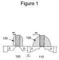
- FIG. 1is a side schematic view of two MOSFETs with different spacer widths adjacent to each other on the same substrate according to the present invention.
- FIG. 2is a side schematic view of n-type MOSFET with a narrower spacer and p-type MOSFET with a wider spacer adjacent to each other on the same substrate according to the present invention.
- FIG. 3( a )is an inverter circuit schematic
- FIG. 3( b )is a top plan view of an on-wafer layout of the inverter circuit having the dual width spacers according to the present invention.
- FIG. 4is a side schematic view of a partially processed MOSFET device structure with gate stacks, extension spacers, extension implants and isolation.
- FIG. 5shows the structure of FIG. 4, after a thin film dielectric 220 is deposited.
- FIG. 6shows the structure of FIG. 5, after another thin film dielectric 230 is deposited.
- FIG. 7shows the structure of FIG. 6, after a photoresist 240 is patterned.
- FIG. 8shows the structure of FIG. 7, after an exposed part of the dielectric 230 is removed, and the photoresist 240 is removed.
- FIG. 9shows the structure of FIG. 8, after a directional etch forming a spacer 260 comprising the dielectric 230 only on the PFET side.
- FIG. 10shows the structure of FIG. 6, after a directional etch forming spacer 270 comprising dielectric 230 on both NFET and PFET.
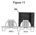
- FIG. 11shows the structure of FIG. 10, after a photoresist 280 is patterned.
- FIG. 12shows the structure of FIG. 11, after an exposed part of dielectric 230 is removed, and the photoresist 280 is removed.
- FIG. 13shows the structure of FIG. 12 or FIG. 9, after a directional etch forming a narrow spacer 300 on the NFET side and L-shape composite spacer 290 on the PFET side.
- FIG. 14shows the structure of FIG. 13, after source/drain implants 310 , 320 and silicide formation 330 .
- FIG. 15is a cross-sectional schematic view of the inventive structure shown in FIG. 14, but further clarifying preferred features S 1 and S 2 of the invention.
- FIG. 1shows two MOSFETs 100 , 110 formed on the same semiconductor substrate 10 having two different spacers 120 , 130 .
- Spacer 120has a smaller width ( 1 ) than the width (W 2 ) of spacer 130 .
- the substrateis a bulk wafer, SOI wafer, GaAs or any type of semiconductor substrate.
- the number of different spacer widthscan be more than two, if necessary to meet the needs of different transistors.
- the PFET 150has a wider spacer 170 than the NFET 140 .
- the spacers 120 , 130 , 160 , 170are schematically shown as single spacers for discussion, but are understood alternatively to include multiple layers (composite spacers).
- the narrower spacer 160allows the optimization of the source/drain implant N+ in NFET in order to minimize known source/drain resistance.
- FIG. 3( a ) and FIG. 3( b )show an example of a circuit and layout using this invention.
- FIG. 3( a )shows the circuit schematic of inverter, while FIG. 3( b ) shows a corresponding on-wafer layout.
- the PFET 150is shown on the top of NFET 140 .
- the spacer widthchanges from wide in the PFET region to narrow in the NFET region.
- the transition region Ris located approximately ( ⁇ 10%) in a middle region between the two devices 140 , 150 .
- FIG. 4 to FIG. 14show two alternative process flows according to the present invention. Both flows start with FIG. 4 where isolations 190 , gate stacks 200 , extension implants 215 and extension spacers 210 are formed in conventional manner. Then, a thin film dielectric 220 (e.g., CVD nitride) is deposited (see FIG. 5). Then, a second film dielectric 230 (e.g. CVD oxide) is also deposited (see FIG. 6). In the first process flow, lithography is applied (FIG. 7). A photoresist 240 covers the PFET side and then part of the dielectric 230 exposed is removed by wet etch or dry etch (FIG. 8). This step leaves another part 250 of the thin film dielectric 230 remaining only on the PFET side. Then, a directional etch is used to form a spacer (S) 260 only on the PFET side (FIG. 9).
- a thin film dielectric 220e.g., CVD n
- FIG. 9The same intermediate structure (FIG. 9) can be achieved by an alternative process flow.
- FIG. 6wherein the second thin film dielectric 230 is deposited.
- a directional etchis applied to form spacers 270 on both NFET and PFET with dielectric 230 (FIG. 10).
- lithographyis applied (FIG. 11).
- a photoresist 280covers the PFET side and the spacers on the NFET side are removed (FIG. 12). The photoresist is removed, which results in spacers only on the PFET side 260 .
- the structure at this stageis identical to the one from previous flow (FIG. 9).
- FIG. 14Another directional etch of the first dielectric 220 from either structure in FIG. 9 or FIG. 12 results in narrow spacers 300 on the NFET side and composite L-shape spacers 290 on the PFET side.
- the final structure(FIG. 14) is formed after n-type 310 and p-type 320 source/drain formations, and silicide formations 330 , with conventional techniques.
- starting wafer substratee.g., bulk, SOI, GaAs
- 3)Deposit thin film dielectric 220 (e.g. CVD nitride). Film thickness should be minimized to result in a highest possible NFET drive current. The nitride thickness determines the final silicide to polysilicon gate spacing S 1 (FIG. 15). The poly to silicide spacing is critical to achieving high NFET drive current—saturated drive current output at drain. Deposited thickness in the range 10 nm-40 nm is preferable.
- thin film dielectric 220e.g. CVD nitride
- Second dielectric film 230e.g. CVD oxide. This film thickness is chosen to independently optimize PFET short channel control—control of leakage current rolloff in the technology L Poly range.
- the film 230 thicknessdetermines the final silicide to poly gate spacing S 2 (FIG. 15).
- the film thickness in a range of 40 nm-100 nmcan be chosen.
- a spacer using the second dielectric film 230 covering only the PFET devicescan now be formed using two independent methods.
- a directional etchis used to form a spacer from the second dielectric film. This spacer 260 is formed only on the PFET devices.
- a directional etchis used to form spacers from the second dielectric film. This spacer is formed on both NFET and PFET devices.
- a second directional etchis used to form a narrow, I-shaped spacer on the NFET device and a wider, L-shaped spacer on the PFET device.
- the final structureis formed after n-type and p-type source/drain formation and silicide formation.
- W 2is in a range of 50 nm to 120 nm
- S 1substantially uniform in a range 1 nm to 20 nm;
- S 2substantially uniform in a range 30 nm to 90nm.
Landscapes
- Metal-Oxide And Bipolar Metal-Oxide Semiconductor Integrated Circuits (AREA)
- Thin Film Transistor (AREA)
- Electrodes Of Semiconductors (AREA)
Abstract
Description
- The present invention relates to semiconductor device structures and, more particularly, to FET device structures formed on the same substrate, and to methods for fabrication.[0001]
- In CMOS technologies, NFET and PFET devices are optimized to achieve required CMOS performance. Very different dopant species are used for NFET and PFET devices, accordingly. These species have very different physical properties such as diffusion rate and maximum activated concentration. In conventional CMOS technologies, both NFET and PFET usually share the same spacer process and topology. In order to optimize CMOS performance, the spacers typically are of one maximum width and are designed to trade-off the performance between NFET and PFET. For example, if Arsenic and Boron are used as the source/drain dopants for NFET and PFET, respectively, it is known that a narrower spacer is better for NFET but a much wider one is better for PFET, because Arsenic diffuses much slower than Boron. In this case, the PFET is a limiting factor. Thus, the maximum width of all spacers is optimized for PFET, trading-off the NFET performance. See, for example: U.S. Pat. No. 5,547,894 (Mandelman et al., issued Aug. 20, 1996, entitled “CMOS Processing with Low High-Current FETS”); U.S. Pat. No. 4,729,006 (Dally et al., issued Mar. 1, 1988, entitled “Sidewall Spacers for CMOS Circuit Stress Relief/Isolation and Method for Making”); and U.S. Pat. No. 4,648,937 (Ogura et al., issued Mar. 10, 1987, entitled “Method of Preventing Asymmetric Etching of Lines in Sub-Micrometer Range Sidewall Images Transfer”); which are all incorporated by reference herein in their entireties.[0002]
- It is a problem, therefore, to optimize spacer width and FET performance for both the NFET and the PFET on the same substrate.[0003]
- The present invention solves this problem by using a dual-spacer width to permit optimizing NFET or PFET device performance independently on the same substrate.[0004]
- It is a principal object of the present invention to optimize performances of two different MOS devices having a common semiconductor substrate.[0005]
- It is an additional object of the present invention to optimize independently the performances of an NFET device and a PFET device formed on one substrate.[0006]
- It is a further object of the present invention to increase the drive current performance of an NFET device while decreasing the short channel effect in a PFET.[0007]
- According to the present invention, a semiconductor device structure includes at least two field effect transistors formed on a same substrate, the first field effect transistor including a spacer having a first width, the second field effect transistor including a spacer having a second width, the first width being different than the second width.[0008]
- The present invention also includes a method (process) for fabricating the semiconductor device structure.[0009]
- These and other objects, advantages and aspects of the invention will be better understood by the following detailed description of a preferred embodiment when taken in conjunction with the accompanying drawings.[0010]
- FIG. 1 is a side schematic view of two MOSFETs with different spacer widths adjacent to each other on the same substrate according to the present invention.[0011]
- FIG. 2 is a side schematic view of n-type MOSFET with a narrower spacer and p-type MOSFET with a wider spacer adjacent to each other on the same substrate according to the present invention.[0012]
- FIG. 3([0013]a) is an inverter circuit schematic, and FIG. 3(b) is a top plan view of an on-wafer layout of the inverter circuit having the dual width spacers according to the present invention.
- FIG. 4 is a side schematic view of a partially processed MOSFET device structure with gate stacks, extension spacers, extension implants and isolation.[0014]
- FIG. 5 shows the structure of FIG. 4, after a thin film dielectric[0015]220 is deposited.
- FIG. 6 shows the structure of FIG. 5, after another thin film dielectric[0016]230 is deposited.
- FIG. 7 shows the structure of FIG. 6, after a[0017]
photoresist 240 is patterned. - FIG. 8 shows the structure of FIG. 7, after an exposed part of the dielectric[0018]230 is removed, and the
photoresist 240 is removed. - FIG. 9 shows the structure of FIG. 8, after a directional etch forming a[0019]
spacer 260 comprising the dielectric230 only on the PFET side. - FIG. 10 shows the structure of FIG. 6, after a directional[0020]
etch forming spacer 270 comprising dielectric230 on both NFET and PFET. - FIG. 11 shows the structure of FIG. 10, after a[0021]
photoresist 280 is patterned. - FIG. 12 shows the structure of FIG. 11, after an exposed part of dielectric[0022]230 is removed, and the
photoresist 280 is removed. - FIG. 13 shows the structure of FIG. 12 or FIG. 9, after a directional etch forming a[0023]
narrow spacer 300 on the NFET side and L-shape composite spacer 290 on the PFET side. - FIG. 14 shows the structure of FIG. 13, after source/[0024]
drain implants silicide formation 330. - FIG. 15 is a cross-sectional schematic view of the inventive structure shown in FIG. 14, but further clarifying preferred features S[0025]1 and S2 of the invention.
- The present invention is described with the final structures (FIGS. 1, 2,[0026]14,15) first, and then with the process sequence. FIG. 1 shows two
MOSFETs same semiconductor substrate 10 having twodifferent spacers Spacer 120 has a smaller width (1) than the width (W2) ofspacer 130. The substrate is a bulk wafer, SOI wafer, GaAs or any type of semiconductor substrate. The number of different spacer widths can be more than two, if necessary to meet the needs of different transistors. According to a preferred embodiment of this invention, there are different spacer widths for NFET140 andPFET 150 as shown in FIG. 2. The PFET150 has awider spacer 170 than the NFET140. Thespacers narrower spacer 160 allows the optimization of the source/drain implant N+ in NFET in order to minimize known source/drain resistance. FIG. 3(a) and FIG. 3(b) show an example of a circuit and layout using this invention. FIG. 3(a) shows the circuit schematic of inverter, while FIG. 3(b) shows a corresponding on-wafer layout. In the figures, thePFET 150 is shown on the top of NFET140. The spacer width changes from wide in the PFET region to narrow in the NFET region. The transition region R is located approximately (±10%) in a middle region between the twodevices - FIG. 4 to FIG. 14 show two alternative process flows according to the present invention. Both flows start with FIG. 4 where[0027]
isolations 190,gate stacks 200,extension implants 215 andextension spacers 210 are formed in conventional manner. Then, a thin film dielectric220 (e.g., CVD nitride) is deposited (see FIG. 5). Then, a second film dielectric230 (e.g. CVD oxide) is also deposited (see FIG. 6). In the first process flow, lithography is applied (FIG. 7). A photoresist240 covers the PFET side and then part of the dielectric230 exposed is removed by wet etch or dry etch (FIG. 8). This step leaves anotherpart 250 of thethin film dielectric 230 remaining only on the PFET side. Then, a directional etch is used to form a spacer (S)260 only on the PFET side (FIG. 9). - The same intermediate structure (FIG. 9) can be achieved by an alternative process flow. Start from FIG. 6, wherein the second[0028]
thin film dielectric 230 is deposited. Then, a directional etch is applied to form spacers270 on both NFET and PFET with dielectric230 (FIG. 10). Then, lithography is applied (FIG. 11). Aphotoresist 280 covers the PFET side and the spacers on the NFET side are removed (FIG. 12). The photoresist is removed, which results in spacers only on thePFET side 260. The structure at this stage is identical to the one from previous flow (FIG. 9). - Another directional etch of the first dielectric[0029]220 from either structure in FIG. 9 or FIG. 12 results in
narrow spacers 300 on the NFET side and composite L-shape spacers 290 on the PFET side. The final structure (FIG. 14) is formed after n-type 310 and p-type 320 source/drain formations, andsilicide formations 330, with conventional techniques. - To recapitulate the alternative preferred process steps according to the present invention:[0030]
- 1) Provide starting wafer substrate (e.g., bulk, SOI, GaAs)[0031]
- 2) Perform conventional CMOS device processing:[0032]
- Device Isolation[0033]
- Gate Stack Formation[0034]
- Extension Implants[0035]
- 3) Deposit thin film dielectric[0036]220 (e.g. CVD nitride). Film thickness should be minimized to result in a highest possible NFET drive current. The nitride thickness determines the final silicide to polysilicon gate spacing S1 (FIG. 15). The poly to silicide spacing is critical to achieving high NFET drive current—saturated drive current output at drain. Deposited thickness in the
range 10 nm-40 nm is preferable. - 4) Deposit second dielectric film[0037]230 (e.g. CVD oxide). This film thickness is chosen to independently optimize PFET short channel control—control of leakage current rolloff in the technology L Poly range. The
film 230 thickness determines the final silicide to poly gate spacing S2 (FIG. 15). The film thickness in a range of 40 nm-100 nm can be chosen. - A spacer using the[0038]
second dielectric film 230 covering only the PFET devices can now be formed using two independent methods. - Process Option #1[0039]
- 5a)[0040]
Pattern photoresist 240 to cover PFET devices and expose NFET devices. Thesecond dielectric film 230 is now removed from NFET devices via a wet or dry etch. Remove thephotoresist 240 by conventional methods. The second dielectric film now covers only the PFET devices. - 5b) A directional etch is used to form a spacer from the second dielectric film. This[0041]
spacer 260 is formed only on the PFET devices. - Process Option #2[0042]
- 5aa) A directional etch is used to form spacers from the second dielectric film. This spacer is formed on both NFET and PFET devices.[0043]
- 5bb) Pattern photoresist to cover PFET devices and expose NFET devices. The spacer is removed from the NFET devices via wet or dry etch. The spacer formed using the second dielectric film covers only the PFET devices.[0044]
- 6) A second directional etch is used to form a narrow, I-shaped spacer on the NFET device and a wider, L-shaped spacer on the PFET device.[0045]
- 7) The final structure is formed after n-type and p-type source/drain formation and silicide formation.[0046]
- Preferably:[0047]
- W[0048]2 is in a range of 50 nm to 120 nm;
- S[0049]1—substantially uniform in a range 1 nm to 20 nm;
- S[0050]2—substantially uniform in a range 30 nm to 90nm.
Claims (10)
Priority Applications (5)
| Application Number | Priority Date | Filing Date | Title |
|---|---|---|---|
| US10/277,907US6806584B2 (en) | 2002-10-21 | 2002-10-21 | Semiconductor device structure including multiple fets having different spacer widths |
| CNA031585469ACN1494153A (en) | 2002-10-21 | 2003-09-18 | Semiconductor device structure and manufacturing method thereof |
| KR1020030065355AKR100544546B1 (en) | 2002-10-21 | 2003-09-20 | SEMICONDUCTOR DEVICE STRUCTURE INCLUDING MULTIPLE FETs HAVING DIFFERENT SPACER WIDTHS |
| JP2003347653AJP2004146824A (en) | 2002-10-21 | 2003-10-06 | Semiconductor device structure and method of manufacturing the same |
| TW092128329ATWI247385B (en) | 2002-10-21 | 2003-10-13 | Semiconductor device structure including multiple FETs having different spacer widths |
Applications Claiming Priority (1)
| Application Number | Priority Date | Filing Date | Title |
|---|---|---|---|
| US10/277,907US6806584B2 (en) | 2002-10-21 | 2002-10-21 | Semiconductor device structure including multiple fets having different spacer widths |
Publications (2)
| Publication Number | Publication Date |
|---|---|
| US20040075151A1true US20040075151A1 (en) | 2004-04-22 |
| US6806584B2 US6806584B2 (en) | 2004-10-19 |
Family
ID=32093369
Family Applications (1)
| Application Number | Title | Priority Date | Filing Date |
|---|---|---|---|
| US10/277,907Expired - LifetimeUS6806584B2 (en) | 2002-10-21 | 2002-10-21 | Semiconductor device structure including multiple fets having different spacer widths |
Country Status (5)
| Country | Link |
|---|---|
| US (1) | US6806584B2 (en) |
| JP (1) | JP2004146824A (en) |
| KR (1) | KR100544546B1 (en) |
| CN (1) | CN1494153A (en) |
| TW (1) | TWI247385B (en) |
Cited By (8)
| Publication number | Priority date | Publication date | Assignee | Title |
|---|---|---|---|---|
| US20050287823A1 (en)* | 2004-06-29 | 2005-12-29 | International Business Machines Corporation | Dual-frequency silicon nitride for spacer application |
| US20060170016A1 (en)* | 2005-02-01 | 2006-08-03 | Freescale Semiconductor Inc. | Asymmetric spacers and asymmetric source/drain extension layers |
| US7105398B2 (en) | 2004-09-16 | 2006-09-12 | International Business Machines Corporation | Method for monitoring lateral encroachment of spacer process on a CD SEM |
| US20070026615A1 (en)* | 2005-07-27 | 2007-02-01 | Sinan Goktepeli | Method of forming a FINFET structure |
| US7304352B2 (en) | 2005-04-21 | 2007-12-04 | International Business Machines Corporation | Alignment insensitive D-cache cell |
| US20080185662A1 (en)* | 2005-10-07 | 2008-08-07 | International Business Machines Corporation | Structure and method for forming asymmetrical overlap capacitance in field effect transistors |
| US20090189193A1 (en)* | 2006-06-30 | 2009-07-30 | Intel Corporation | Selective spacer formation on transistors of different classes on the same device |
| US20100187636A1 (en)* | 2005-11-14 | 2010-07-29 | International Business Machines Corporation | Method to increase strain enhancement with spacerless fet and dual liner process |
Families Citing this family (30)
| Publication number | Priority date | Publication date | Assignee | Title |
|---|---|---|---|---|
| US7279746B2 (en)* | 2003-06-30 | 2007-10-09 | International Business Machines Corporation | High performance CMOS device structures and method of manufacture |
| US6869866B1 (en)* | 2003-09-22 | 2005-03-22 | International Business Machines Corporation | Silicide proximity structures for CMOS device performance improvements |
| US7176522B2 (en)* | 2003-11-25 | 2007-02-13 | Taiwan Semiconductor Manufacturing Company, Ltd. | Semiconductor device having high drive current and method of manufacturing thereof |
| US7064396B2 (en)* | 2004-03-01 | 2006-06-20 | Freescale Semiconductor, Inc. | Integrated circuit with multiple spacer insulating region widths |
| TWI463526B (en)* | 2004-06-24 | 2014-12-01 | Ibm | Method for improving stress-induced CMOS components and components prepared by the method |
| JP4746332B2 (en)* | 2005-03-10 | 2011-08-10 | Okiセミコンダクタ株式会社 | Manufacturing method of semiconductor device |
| US7282426B2 (en)* | 2005-03-29 | 2007-10-16 | Freescale Semiconductor, Inc. | Method of forming a semiconductor device having asymmetric dielectric regions and structure thereof |
| KR101252262B1 (en)* | 2005-06-30 | 2013-04-08 | 어드밴스드 마이크로 디바이시즈, 인코포레이티드 | Technique for forming contact insulation layers silicide regions with different characteristics |
| DE102005030583B4 (en)* | 2005-06-30 | 2010-09-30 | Advanced Micro Devices, Inc., Sunnyvale | Method for producing contact insulation layers and silicide regions having different properties of a semiconductor device and semiconductor device |
| US7655511B2 (en) | 2005-11-03 | 2010-02-02 | International Business Machines Corporation | Gate electrode stress control for finFET performance enhancement |
| US7759206B2 (en)* | 2005-11-29 | 2010-07-20 | International Business Machines Corporation | Methods of forming semiconductor devices using embedded L-shape spacers |
| US7776695B2 (en)* | 2006-01-09 | 2010-08-17 | International Business Machines Corporation | Semiconductor device structure having low and high performance devices of same conductive type on same substrate |
| US7635620B2 (en) | 2006-01-10 | 2009-12-22 | International Business Machines Corporation | Semiconductor device structure having enhanced performance FET device |
| US7323373B2 (en)* | 2006-01-25 | 2008-01-29 | Freescale Semiconductor, Inc. | Method of forming a semiconductor device with decreased undercutting of semiconductor material |
| JP2007220755A (en)* | 2006-02-14 | 2007-08-30 | Toshiba Corp | Semiconductor device and manufacturing method thereof |
| US20070249112A1 (en)* | 2006-04-21 | 2007-10-25 | International Business Machines Corporation | Differential spacer formation for a field effect transistor |
| US8354726B2 (en)* | 2006-05-19 | 2013-01-15 | Panasonic Corporation | Semiconductor device and method for fabricating the same |
| US7790540B2 (en) | 2006-08-25 | 2010-09-07 | International Business Machines Corporation | Structure and method to use low k stress liner to reduce parasitic capacitance |
| JP4970185B2 (en)* | 2007-07-30 | 2012-07-04 | 株式会社東芝 | Semiconductor device and manufacturing method thereof |
| US8115254B2 (en) | 2007-09-25 | 2012-02-14 | International Business Machines Corporation | Semiconductor-on-insulator structures including a trench containing an insulator stressor plug and method of fabricating same |
| DE102007052220B4 (en)* | 2007-10-31 | 2015-04-09 | Globalfoundries Inc. | A dopant profile adjustment method for MOS devices by adjusting a spacer width prior to implantation |
| US8492846B2 (en) | 2007-11-15 | 2013-07-23 | International Business Machines Corporation | Stress-generating shallow trench isolation structure having dual composition |
| US7728392B2 (en)* | 2008-01-03 | 2010-06-01 | International Business Machines Corporation | SRAM device structure including same band gap transistors having gate stacks with high-K dielectrics and same work function |
| KR20100009869A (en)* | 2008-07-21 | 2010-01-29 | 삼성전자주식회사 | Cmos transistor and method of manufacturing the same |
| JP5444694B2 (en)* | 2008-11-12 | 2014-03-19 | ソニー株式会社 | Solid-state imaging device, manufacturing method thereof, and imaging device |
| US8592325B2 (en)* | 2010-01-11 | 2013-11-26 | International Business Machines Corporation | Insulating layers on different semiconductor materials |
| US8598006B2 (en) | 2010-03-16 | 2013-12-03 | International Business Machines Corporation | Strain preserving ion implantation methods |
| US8531001B2 (en)* | 2011-06-12 | 2013-09-10 | International Business Machines Corporation | Complementary bipolar inverter |
| JP6275559B2 (en)* | 2014-06-13 | 2018-02-07 | ルネサスエレクトロニクス株式会社 | Semiconductor device and manufacturing method thereof |
| US10096523B2 (en) | 2015-11-30 | 2018-10-09 | Taiwan Semiconductor Manufacturing Company, Ltd. | Spacer structure and manufacturing method thereof |
Citations (2)
| Publication number | Priority date | Publication date | Assignee | Title |
|---|---|---|---|---|
| US6064096A (en)* | 1996-11-27 | 2000-05-16 | Lg Semicon Co., Ltd. | Semiconductor LDD device having halo impurity regions |
| US6512273B1 (en)* | 2000-01-28 | 2003-01-28 | Advanced Micro Devices, Inc. | Method and structure for improving hot carrier immunity for devices with very shallow junctions |
Family Cites Families (20)
| Publication number | Priority date | Publication date | Assignee | Title |
|---|---|---|---|---|
| US4577391A (en)* | 1984-07-27 | 1986-03-25 | Monolithic Memories, Inc. | Method of manufacturing CMOS devices |
| US4648937A (en) | 1985-10-30 | 1987-03-10 | International Business Machines Corporation | Method of preventing asymmetric etching of lines in sub-micrometer range sidewall images transfer |
| US4729006A (en) | 1986-03-17 | 1988-03-01 | International Business Machines Corporation | Sidewall spacers for CMOS circuit stress relief/isolation and method for making |
| JPH03180058A (en)* | 1989-12-08 | 1991-08-06 | Sony Corp | Semiconductor device |
| US5296401A (en)* | 1990-01-11 | 1994-03-22 | Mitsubishi Denki Kabushiki Kaisha | MIS device having p channel MOS device and n channel MOS device with LDD structure and manufacturing method thereof |
| KR950000141B1 (en)* | 1990-04-03 | 1995-01-10 | 미쓰비시 뎅끼 가부시끼가이샤 | Semiconductor device & manufacturing method thereof |
| KR940005802B1 (en)* | 1991-07-09 | 1994-06-23 | 삼성전자 주식회사 | Cmos semiconductor device and method of making the same |
| US5786247A (en)* | 1994-05-06 | 1998-07-28 | Vlsi Technology, Inc. | Low voltage CMOS process with individually adjustable LDD spacers |
| US5491099A (en) | 1994-08-29 | 1996-02-13 | United Microelectronics Corporation | Method of making silicided LDD with recess in semiconductor substrate |
| US5547894A (en) | 1995-12-21 | 1996-08-20 | International Business Machines Corporation | CMOS processing with low and high-current FETs |
| US6028339A (en)* | 1996-08-29 | 2000-02-22 | International Business Machines Corporation | Dual work function CMOS device |
| JP2982895B2 (en)* | 1997-02-06 | 1999-11-29 | 日本電気株式会社 | CMOS semiconductor device and method of manufacturing the same |
| JPH10242420A (en)* | 1997-02-27 | 1998-09-11 | Toshiba Corp | Semiconductor device and manufacturing method thereof |
| US5763312A (en) | 1997-05-05 | 1998-06-09 | Vanguard International Semiconductor Corporation | Method of fabricating LDD spacers in MOS devices with double spacers and device manufactured thereby |
| JP3180058B2 (en) | 1997-07-15 | 2001-06-25 | 住友ゴム工業株式会社 | Radial tires for heavy loads |
| US5863824A (en)* | 1997-12-18 | 1999-01-26 | Advanced Micro Devices | Method of forming semiconductor devices using gate electrode length and spacer width for controlling drivecurrent strength |
| US5899722A (en) | 1998-05-22 | 1999-05-04 | Taiwan Semiconductor Manufacturing Company Ltd. | Method of forming dual spacer for self aligned contact integration |
| US6248623B1 (en) | 1999-11-12 | 2001-06-19 | United Microelectronics Corp. | Method for manufacturing embedded memory with different spacer widths |
| JP3532134B2 (en) | 2000-01-31 | 2004-05-31 | シャープ株式会社 | Method for manufacturing semiconductor device |
| KR100327347B1 (en)* | 2000-07-22 | 2002-03-06 | Samsung Electronics Co Ltd | Metal oxide semiconductor field effect transistor having reduced resistance between source and drain and fabricating method thereof |
- 2002
- 2002-10-21USUS10/277,907patent/US6806584B2/ennot_activeExpired - Lifetime
- 2003
- 2003-09-18CNCNA031585469Apatent/CN1494153A/enactivePending
- 2003-09-20KRKR1020030065355Apatent/KR100544546B1/ennot_activeExpired - Fee Related
- 2003-10-06JPJP2003347653Apatent/JP2004146824A/enactivePending
- 2003-10-13TWTW092128329Apatent/TWI247385B/ennot_activeIP Right Cessation
Patent Citations (2)
| Publication number | Priority date | Publication date | Assignee | Title |
|---|---|---|---|---|
| US6064096A (en)* | 1996-11-27 | 2000-05-16 | Lg Semicon Co., Ltd. | Semiconductor LDD device having halo impurity regions |
| US6512273B1 (en)* | 2000-01-28 | 2003-01-28 | Advanced Micro Devices, Inc. | Method and structure for improving hot carrier immunity for devices with very shallow junctions |
Cited By (18)
| Publication number | Priority date | Publication date | Assignee | Title |
|---|---|---|---|---|
| US20050287823A1 (en)* | 2004-06-29 | 2005-12-29 | International Business Machines Corporation | Dual-frequency silicon nitride for spacer application |
| US7202187B2 (en) | 2004-06-29 | 2007-04-10 | International Business Machines Corporation | Method of forming sidewall spacer using dual-frequency plasma enhanced CVD |
| US7358130B2 (en) | 2004-09-16 | 2008-04-15 | International Business Machines Corporation | Method for monitoring lateral encroachment of spacer process on a CD SEM |
| US7105398B2 (en) | 2004-09-16 | 2006-09-12 | International Business Machines Corporation | Method for monitoring lateral encroachment of spacer process on a CD SEM |
| US20060252197A1 (en)* | 2004-09-16 | 2006-11-09 | International Business Machine Corporation | Method for monitoring lateral encroachment of spacer process on a CD SEM |
| US20060170016A1 (en)* | 2005-02-01 | 2006-08-03 | Freescale Semiconductor Inc. | Asymmetric spacers and asymmetric source/drain extension layers |
| US7585735B2 (en) | 2005-02-01 | 2009-09-08 | Freescale Semiconductor, Inc. | Asymmetric spacers and asymmetric source/drain extension layers |
| US7304352B2 (en) | 2005-04-21 | 2007-12-04 | International Business Machines Corporation | Alignment insensitive D-cache cell |
| US20070026615A1 (en)* | 2005-07-27 | 2007-02-01 | Sinan Goktepeli | Method of forming a FINFET structure |
| US7323389B2 (en) | 2005-07-27 | 2008-01-29 | Freescale Semiconductor, Inc. | Method of forming a FINFET structure |
| US20080185662A1 (en)* | 2005-10-07 | 2008-08-07 | International Business Machines Corporation | Structure and method for forming asymmetrical overlap capacitance in field effect transistors |
| US20100187636A1 (en)* | 2005-11-14 | 2010-07-29 | International Business Machines Corporation | Method to increase strain enhancement with spacerless fet and dual liner process |
| EP1949435B1 (en)* | 2005-11-14 | 2013-11-20 | International Business Machines Corporation | Structure and method to increase strain enhancement with spacerless fet and dual liner process |
| US20090189193A1 (en)* | 2006-06-30 | 2009-07-30 | Intel Corporation | Selective spacer formation on transistors of different classes on the same device |
| US20110157854A1 (en)* | 2006-06-30 | 2011-06-30 | Giuseppe Curello | Selective spacer formation on transistors of different classes on the same device |
| KR101065827B1 (en)* | 2006-06-30 | 2011-09-20 | 인텔 코포레이션 | Methods, Devices, and Systems for Selective Spacer Formation on Different Kinds of Transistors on the Same Device |
| US8154067B2 (en) | 2006-06-30 | 2012-04-10 | Intel Corporation | Selective spacer formation on transistors of different classes on the same device |
| US8174060B2 (en) | 2006-06-30 | 2012-05-08 | Intel Corporation | Selective spacer formation on transistors of different classes on the same device |
Also Published As
| Publication number | Publication date |
|---|---|
| TWI247385B (en) | 2006-01-11 |
| KR20040034391A (en) | 2004-04-28 |
| US6806584B2 (en) | 2004-10-19 |
| KR100544546B1 (en) | 2006-01-24 |
| JP2004146824A (en) | 2004-05-20 |
| CN1494153A (en) | 2004-05-05 |
| TW200406881A (en) | 2004-05-01 |
Similar Documents
| Publication | Publication Date | Title |
|---|---|---|
| US6806584B2 (en) | Semiconductor device structure including multiple fets having different spacer widths | |
| US7436029B2 (en) | High performance CMOS device structures and method of manufacture | |
| US7214629B1 (en) | Strain-silicon CMOS with dual-stressed film | |
| US6759717B2 (en) | CMOS integrated circuit device with LDD n-channel transistor and non-LDD p-channel transistor | |
| US8124472B2 (en) | Manufacturing method of a semiconductor device | |
| US7018891B2 (en) | Ultra-thin Si channel CMOS with improved series resistance | |
| CN101796641B (en) | Channel Strain Design in Field Effect Transistors | |
| US8502325B2 (en) | Metal high-K transistor having silicon sidewalls for reduced parasitic capacitance | |
| US5643815A (en) | Super self-align process for fabricating submicron CMOS using micron design rule fabrication equipment | |
| US9281246B2 (en) | Strain adjustment in the formation of MOS devices | |
| CN112542456A (en) | Field effect transistor with independently tuned threshold voltages | |
| US7545004B2 (en) | Method and structure for forming strained devices | |
| US7151031B2 (en) | Methods of fabricating semiconductor devices having gate insulating layers with differing thicknesses | |
| US6265253B1 (en) | Aluminum disposable spacer to reduce mask count in CMOS transistor formation | |
| US20040137373A1 (en) | Method for forming multiple spacer widths | |
| US11973130B2 (en) | Method of forming asymmetric differential spacers for optimized MOSFET performance and optimized MOSFET and SONOS co-integration | |
| KR100415191B1 (en) | Method for fabricating asymmetric cmos transistor | |
| KR0179860B1 (en) | Method of manufacturing c-mos element | |
| KR0165421B1 (en) | Process of fabricating mos transistor | |
| JPH0341773A (en) | Semiconductor device and manufacture thereof | |
| KR100861358B1 (en) | Method of Forming Semiconductor Memory Device | |
| SE517452C2 (en) | Metal oxide semiconductor device and method for its manufacture | |
| JPH045831A (en) | Manufacture of mos field-effect transistor | |
| JPH05110084A (en) | Semiconductor device and manufacture thereof |
Legal Events
| Date | Code | Title | Description |
|---|---|---|---|
| AS | Assignment | Owner name:INTERNATIONAL BUSINESS MACHINES CORPORATION, NEW Y Free format text:ASSIGNMENT OF ASSIGNORS INTEREST;ASSIGNORS:FUNG, KA HING;GILBERT, PERCY V.;REEL/FRAME:013485/0256;SIGNING DATES FROM 20021011 TO 20021018 | |
| FEPP | Fee payment procedure | Free format text:PAYOR NUMBER ASSIGNED (ORIGINAL EVENT CODE: ASPN); ENTITY STATUS OF PATENT OWNER: LARGE ENTITY | |
| STCF | Information on status: patent grant | Free format text:PATENTED CASE | |
| FPAY | Fee payment | Year of fee payment:4 | |
| REMI | Maintenance fee reminder mailed | ||
| FPAY | Fee payment | Year of fee payment:8 | |
| SULP | Surcharge for late payment | Year of fee payment:7 | |
| AS | Assignment | Owner name:GLOBALFOUNDRIES U.S. 2 LLC, NEW YORK Free format text:ASSIGNMENT OF ASSIGNORS INTEREST;ASSIGNOR:INTERNATIONAL BUSINESS MACHINES CORPORATION;REEL/FRAME:036550/0001 Effective date:20150629 | |
| AS | Assignment | Owner name:GLOBALFOUNDRIES INC., CAYMAN ISLANDS Free format text:ASSIGNMENT OF ASSIGNORS INTEREST;ASSIGNORS:GLOBALFOUNDRIES U.S. 2 LLC;GLOBALFOUNDRIES U.S. INC.;REEL/FRAME:036779/0001 Effective date:20150910 | |
| FPAY | Fee payment | Year of fee payment:12 | |
| AS | Assignment | Owner name:AURIGA INNOVATIONS, INC., CANADA Free format text:ASSIGNMENT OF ASSIGNORS INTEREST;ASSIGNOR:GLOBALFOUNDRIES INC.;REEL/FRAME:041741/0358 Effective date:20161207 |