US20040075122A1 - Double and triple gate MOSFET devices and methods for making same - Google Patents
Double and triple gate MOSFET devices and methods for making sameDownload PDFInfo
- Publication number
- US20040075122A1 US20040075122A1US10/274,961US27496102AUS2004075122A1US 20040075122 A1US20040075122 A1US 20040075122A1US 27496102 AUS27496102 AUS 27496102AUS 2004075122 A1US2004075122 A1US 2004075122A1
- Authority
- US
- United States
- Prior art keywords
- gate
- fin
- forming
- mosfet
- gate structure
- Prior art date
- Legal status (The legal status is an assumption and is not a legal conclusion. Google has not performed a legal analysis and makes no representation as to the accuracy of the status listed.)
- Granted
Links
- 238000000034methodMethods0.000titleclaimsdescription34
- 239000004065semiconductorSubstances0.000claimsabstractdescription14
- 230000005669field effectEffects0.000claimsabstractdescription6
- 229910044991metal oxideInorganic materials0.000claimsabstractdescription6
- 150000004706metal oxidesChemical class0.000claimsabstractdescription6
- 239000010410layerSubstances0.000claimsdescription49
- XUIMIQQOPSSXEZ-UHFFFAOYSA-NSiliconChemical compound[Si]XUIMIQQOPSSXEZ-UHFFFAOYSA-N0.000claimsdescription14
- 239000003989dielectric materialSubstances0.000claimsdescription14
- 229910052710siliconInorganic materials0.000claimsdescription14
- 239000010703siliconSubstances0.000claimsdescription14
- 239000000463materialSubstances0.000claimsdescription12
- 239000000758substrateSubstances0.000claimsdescription8
- 238000000151depositionMethods0.000claimsdescription6
- 239000011229interlayerSubstances0.000claimsdescription3
- 238000000059patterningMethods0.000claims2
- 238000012545processingMethods0.000description11
- 238000004519manufacturing processMethods0.000description7
- 230000008569processEffects0.000description7
- 238000005530etchingMethods0.000description4
- 229910052581Si3N4Inorganic materials0.000description3
- HQVNEWCFYHHQES-UHFFFAOYSA-Nsilicon nitrideChemical compoundN12[Si]34N5[Si]62N3[Si]51N64HQVNEWCFYHHQES-UHFFFAOYSA-N0.000description3
- PXHVJJICTQNCMI-UHFFFAOYSA-NNickelChemical compound[Ni]PXHVJJICTQNCMI-UHFFFAOYSA-N0.000description2
- KDLHZDBZIXYQEI-UHFFFAOYSA-NPalladiumChemical compound[Pd]KDLHZDBZIXYQEI-UHFFFAOYSA-N0.000description2
- VYPSYNLAJGMNEJ-UHFFFAOYSA-NSilicium dioxideChemical compoundO=[Si]=OVYPSYNLAJGMNEJ-UHFFFAOYSA-N0.000description2
- BOTDANWDWHJENH-UHFFFAOYSA-NTetraethyl orthosilicateChemical compoundCCO[Si](OCC)(OCC)OCCBOTDANWDWHJENH-UHFFFAOYSA-N0.000description2
- 238000005229chemical vapour depositionMethods0.000description2
- 238000010894electron beam technologyMethods0.000description2
- 229910052751metalInorganic materials0.000description2
- 239000002184metalSubstances0.000description2
- BASFCYQUMIYNBI-UHFFFAOYSA-NplatinumChemical compound[Pt]BASFCYQUMIYNBI-UHFFFAOYSA-N0.000description2
- 238000005498polishingMethods0.000description2
- 230000001681protective effectEffects0.000description2
- ZOKXTWBITQBERF-UHFFFAOYSA-NMolybdenumChemical compound[Mo]ZOKXTWBITQBERF-UHFFFAOYSA-N0.000description1
- KJTLSVCANCCWHF-UHFFFAOYSA-NRutheniumChemical compound[Ru]KJTLSVCANCCWHF-UHFFFAOYSA-N0.000description1
- 229910000577Silicon-germaniumInorganic materials0.000description1
- RTAQQCXQSZGOHL-UHFFFAOYSA-NTitaniumChemical compound[Ti]RTAQQCXQSZGOHL-UHFFFAOYSA-N0.000description1
- NRTOMJZYCJJWKI-UHFFFAOYSA-NTitanium nitrideChemical compound[Ti]#NNRTOMJZYCJJWKI-UHFFFAOYSA-N0.000description1
- LEVVHYCKPQWKOP-UHFFFAOYSA-N[Si].[Ge]Chemical compound[Si].[Ge]LEVVHYCKPQWKOP-UHFFFAOYSA-N0.000description1
- 229910052782aluminiumInorganic materials0.000description1
- XAGFODPZIPBFFR-UHFFFAOYSA-NaluminiumChemical compound[Al]XAGFODPZIPBFFR-UHFFFAOYSA-N0.000description1
- 230000015572biosynthetic processEffects0.000description1
- 150000001875compoundsChemical class0.000description1
- 230000008878couplingEffects0.000description1
- 238000010168coupling processMethods0.000description1
- 238000005859coupling reactionMethods0.000description1
- 230000001419dependent effectEffects0.000description1
- 230000008021depositionEffects0.000description1
- 230000000694effectsEffects0.000description1
- 238000000609electron-beam lithographyMethods0.000description1
- 239000012212insulatorSubstances0.000description1
- 238000001459lithographyMethods0.000description1
- 238000012986modificationMethods0.000description1
- 230000004048modificationEffects0.000description1
- 229910052750molybdenumInorganic materials0.000description1
- 239000011733molybdenumSubstances0.000description1
- 229910052759nickelInorganic materials0.000description1
- 150000004767nitridesChemical class0.000description1
- 238000005457optimizationMethods0.000description1
- 238000012856packingMethods0.000description1
- 229910052763palladiumInorganic materials0.000description1
- 229910052697platinumInorganic materials0.000description1
- 229910021420polycrystalline siliconInorganic materials0.000description1
- 230000009467reductionEffects0.000description1
- 229910052703rhodiumInorganic materials0.000description1
- 239000010948rhodiumSubstances0.000description1
- MHOVAHRLVXNVSD-UHFFFAOYSA-Nrhodium atomChemical compound[Rh]MHOVAHRLVXNVSD-UHFFFAOYSA-N0.000description1
- 229910052707rutheniumInorganic materials0.000description1
- 229910001925ruthenium oxideInorganic materials0.000description1
- WOCIAKWEIIZHES-UHFFFAOYSA-Nruthenium(iv) oxideChemical compoundO=[Ru]=OWOCIAKWEIIZHES-UHFFFAOYSA-N0.000description1
- 235000012239silicon dioxideNutrition0.000description1
- 239000000377silicon dioxideSubstances0.000description1
- -1structuresSubstances0.000description1
- 239000000126substanceSubstances0.000description1
- 229910052715tantalumInorganic materials0.000description1
- GUVRBAGPIYLISA-UHFFFAOYSA-Ntantalum atomChemical compound[Ta]GUVRBAGPIYLISA-UHFFFAOYSA-N0.000description1
- MZLGASXMSKOWSE-UHFFFAOYSA-Ntantalum nitrideChemical compound[Ta]#NMZLGASXMSKOWSE-UHFFFAOYSA-N0.000description1
- 229910052719titaniumInorganic materials0.000description1
- 239000010936titaniumSubstances0.000description1
- WFKWXMTUELFFGS-UHFFFAOYSA-NtungstenChemical compound[W]WFKWXMTUELFFGS-UHFFFAOYSA-N0.000description1
- 229910052721tungstenInorganic materials0.000description1
- 239000010937tungstenSubstances0.000description1
Images


Classifications
- H—ELECTRICITY
- H10—SEMICONDUCTOR DEVICES; ELECTRIC SOLID-STATE DEVICES NOT OTHERWISE PROVIDED FOR
- H10D—INORGANIC ELECTRIC SEMICONDUCTOR DEVICES
- H10D30/00—Field-effect transistors [FET]
- H10D30/60—Insulated-gate field-effect transistors [IGFET]
- H10D30/62—Fin field-effect transistors [FinFET]
- H—ELECTRICITY
- H10—SEMICONDUCTOR DEVICES; ELECTRIC SOLID-STATE DEVICES NOT OTHERWISE PROVIDED FOR
- H10D—INORGANIC ELECTRIC SEMICONDUCTOR DEVICES
- H10D30/00—Field-effect transistors [FET]
- H10D30/01—Manufacture or treatment
- H10D30/021—Manufacture or treatment of FETs having insulated gates [IGFET]
- H10D30/024—Manufacture or treatment of FETs having insulated gates [IGFET] of fin field-effect transistors [FinFET]
- H10D30/0245—Manufacture or treatment of FETs having insulated gates [IGFET] of fin field-effect transistors [FinFET] by further thinning the channel after patterning the channel, e.g. using sacrificial oxidation on fins
- H—ELECTRICITY
- H10—SEMICONDUCTOR DEVICES; ELECTRIC SOLID-STATE DEVICES NOT OTHERWISE PROVIDED FOR
- H10D—INORGANIC ELECTRIC SEMICONDUCTOR DEVICES
- H10D30/00—Field-effect transistors [FET]
- H10D30/60—Insulated-gate field-effect transistors [IGFET]
- H10D30/62—Fin field-effect transistors [FinFET]
- H10D30/6215—Fin field-effect transistors [FinFET] having multiple independently-addressable gate electrodes
- H—ELECTRICITY
- H10—SEMICONDUCTOR DEVICES; ELECTRIC SOLID-STATE DEVICES NOT OTHERWISE PROVIDED FOR
- H10D—INORGANIC ELECTRIC SEMICONDUCTOR DEVICES
- H10D30/00—Field-effect transistors [FET]
- H10D30/60—Insulated-gate field-effect transistors [IGFET]
- H10D30/67—Thin-film transistors [TFT]
- H10D30/6729—Thin-film transistors [TFT] characterised by the electrodes
- H10D30/673—Thin-film transistors [TFT] characterised by the electrodes characterised by the shapes, relative sizes or dispositions of the gate electrodes
Definitions
- the present inventionrelates generally to semiconductor manufacturing and, more particularly, to double and triple gate metal-oxide semiconductor field-effect transistor (MOSFET) devices and methods of making these devices.
- MOSFETmetal-oxide semiconductor field-effect transistor
- Double-gate MOSFETsrepresent new devices that are candidates for succeeding existing planar MOSFETs.
- double-gate MOSFETsthe use of two gates to control the channel significantly suppresses short-channel effects.
- a FinFETis a recent double-gate structure that includes a channel formed in a vertical fin controlled by a self-aligned double gate. The fin may be made thin enough such that the two gates can together control the entire fully depleted channel.
- the FinFETis similar to existing planar MOSFET in layout and fabrication techniques.
- the FinFETalso provides a range of channel lengths, CMOS compatibility, and large packing density compared to other double-gate structures.
- Implementations consistent with the principles of the inventionprovide double gate and triple gate FinFET devices. Unlike conventional designs, each of the gates in the FinFET can independently control the FinFET's channel.
- a method for forming gates in a MOSFETincludes forming a fin structure, forming a first gate structure on top of the fin structure, and forming a second gate structure that surrounds the fin structure and the first gate structure.
- a method for forming gates in a MOSFETincludes forming a fin, forming a first gate on top of the fin, forming a second gate that surrounds the fin and the first gate, and removing a portion of the second gate to expose the first gate, the removing causing the second gate to be split into separate gate structures.
- a double gate MOSFETincludes a fin, a first gate structure and a second gate structure.
- the first gate structureis formed on top of the fin.
- the second gate structuresurrounds the fin and the first gate structure.
- a triple gate MOSFETincludes a fin, a first gate structure formed on top of the fin, a second gate structure formed adjacent the fin, and a third gate structure formed adjacent the fin and opposite the second gate structure.
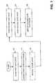
- FIG. 1illustrates an exemplary process for fabricating a double gate MOSFET in an implementation consistent with the principles of the invention
- FIGS. 2 - 4illustrate exemplary cross-sectional views of a double gate MOSFET fabricated according to the processing described in FIG. 1;
- FIG. 5illustrates an exemplary process for fabricating a triple gate MOSFET in an implementation consistent with the principles of the invention
- FIGS. 6 - 8illustrate exemplary cross-sectional views of a triple gate MOSFET fabricated according to the processing described in FIG. 5;
- FIG. 9illustrates an exemplary structure for adding mobility to a fin in an implementation consistent with the principles of the invention.
- FIGS. 10 - 12illustrate exemplary cross-sectional views of a MOSFET fabricated to include a thin fin body structure.
- Implementations consistent with the principles of the inventionprovide double gate and triple gate FinFET devices. Unlike conventional designs, each of the gates in the FinFET can independently control the fin channel.
- FIG. 1illustrates an exemplary process for fabricating a double gate MOSFET in an implementation consistent with the principles of the invention.
- FIGS. 2 - 4illustrate exemplary cross-sectional views of a MOSFET fabricated according to the processing described in FIG. 1.
- processingmay begin with a silicon on insulator (SOI) structure that includes a silicon substrate 200 , a buried oxide layer 210 and a silicon layer 220 on the buried oxide layer 210 .
- Buried oxide layer 210 and silicon layer 220may be formed on substrate 200 in a conventional manner.
- the thickness of the buried oxide layermay range, for example, from about 100 ⁇ to 2000 ⁇ .
- Silicon layer 220 thicknessmay range from about 200 ⁇ to 1000 ⁇ . It will be appreciated that silicon layer 220 is used to form the fin.
- a gate oxide layer 230may be deposited or thermally grown on silicon layer 220 (act 105 ). Gate oxide layer 230 may be formed at a thickness ranging from approximately 5 ⁇ to 50 ⁇ . Alternatively, other gate dielectric materials, such as high-K dielectric materials, may be used. In one implementation, nitrided oxide may be used as the gate dielectric material.
- a gate electrode layer 240may be deposited over gate oxide layer 230 for forming the first gate (act 110 ). A number of materials may be used for gate electrode 240 .
- gate electrode 240may be made from a metal (e.g., tungsten, tantalum, aluminum, nickel, ruthenium, rhodium, palladium, platinum, titanium, molybdenum, etc.), a metal containing a compound (e.g., titanium nitride, tantalum nitride, ruthenium oxide, etc.), or a doped semiconductor (e.g., polycrystalline silicon, polycrystalline silicon-germanium, etc.).
- a cover layer 250may optionally be formed on top of gate electrode 240 to aid in pattern optimization or chemical-mechanical polishing (CMP) (act 115 ).
- Cover layer 250may, for example, include a silicon nitride (SiN) material or some other similar type of material capable of protecting the gate electrode during the fabrication process. Cover layer 250 may be deposited, for example, by chemical vapor deposition (CVD) at a thickness ranging from approximately 30 ⁇ to 200 ⁇ .
- CVDchemical vapor deposition
- Fin 220 and first gate 230 / 240may be patterned by conventional lithographic techniques (e.g., electron beam (EB) lithography) (act 120 ). Fin 220 and first gate 230 may then be etched using well-known etching techniques (act 120 ). The resulting structure 300 is illustrated in FIG. 3. The width of fin 220 and first gate 230 in structure 300 may be approximately 50 ⁇ to 500 ⁇ .
- lithographic techniquese.g., electron beam (EB) lithography
- a second gatemay be formed.
- a second gate oxide layer 410may be deposited or thermally grown (act 125 ), as illustrated in FIG. 4.
- Gate oxide layer 410may be deposited or grown to a thickness of approximately 5 ⁇ to 50 ⁇ .
- other gate dielectric materialsmay be used.
- any high-K dielectric materialmay be used as the gate dielectric material.
- a second gate electrode layer 420may be deposited over gate oxide layer 410 for forming the second gate (act 130 ). Similar to first gate electrode 240 , a number of materials may be used for second gate electrode 420 .
- this structure 400allows two gates (i.e., gates 240 and 420 ) to independently control the fin channel.
- Conventional MOSFET fabrication processingcan be utilized to complete the transistor (e.g., forming the source and drain regions), contacts, interconnects and inter-level dielectrics for the double gate MOSFET.
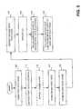
- FIG. 5illustrates an exemplary process for fabricating a triple gate MOSFET in an implementation consistent with the principles of the invention.
- FIGS. 6 - 8illustrate exemplary cross-sectional views of a triple gate MOSFET fabricated according to the processing described in FIG. 5. Processing may begin by performing acts 105 - 130 described above with respect to FIG. 1. After gate electrode layer 420 has been deposited, an interlayer dielectric (ILD) 610 may be deposited over second gate electrode layer 410 (act 505 ), as illustrated in FIG. 6. ILD 610 may include, for example, tetraethoxy silane (TEOS) or another similar type of material. The thickness of ILD 610 may be such that it extends above the height of second gate electrode 420 .
- ILDinterlayer dielectric
- CMPChemical-mechanical polishing
- second gate electrode 420may be split to form two separate gate structures, namely gates 720 and 730 .
- a triple gate MOSFETmay be formed, where the first gate electrode 240 acts as a third gate 710 .
- Gates 710 - 730may each independently control fin 220 .
- gates 720 and 730may be etched back (act 515 ), as illustrated in FIG. 8, using known techniques.
- Conventional MOSFET fabrication processingcan be utilized to complete the transistor (e.g., forming the source and drain regions), contacts, interconnects and inter-level dielectrics for the triple gate MOSFET.
- Mobilityis an important attribute for improving transistor performance. Mobility may be affected by the state of the strain (or stress) in the film. For example, tensile strain is good for electron mobility, while compressive stress may aid hole mobility.
- FIG. 9illustrates an exemplary structure for adding mobility to a fin.
- a fin structure 910may be formed by forming a silicon layer on a semiconductor substrate.
- the semiconductor substratemay be a SOI structure including an insulating layer, such as a buried oxide layer, formed at a thickness ranging from 100 ⁇ to 2000 ⁇ . Processing for forming a semiconductor substrate, having a buried oxide layer, is well known in the integrated circuit fabrication arts.
- a highly stressed film(referred to hereinafter as a “capping layer”) 920 may then be formed on top of fin structure 910 .
- capping layer 920may be formed from, for example, a nitride-based material at a thickness of approximately 100 ⁇ to 1000 ⁇ . Other materials may alternatively be used. Capping layer 920 remains after fin 910 is etched so that fin 910 is strained to improve mobility.
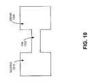
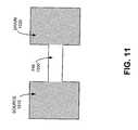
- FIGS. 10 - 12illustrate exemplary cross-sectional views of a MOSFET fabricated to include a thin fin body structure.
- a source region 1010 , a drain region 1020 , and a fin structure 1030may be formed via conventional fabrication techniques.
- an SOI structuremay include an insulating layer (e.g., a buried oxide layer) formed on a semiconductor substrate.
- a silicon filmmay be formed on the SOI structure.
- a hard maske.g., silicon dioxide
- Source and drain regions 1010 and 1020may then be formed in a similar manner.
- source region 1010 , drain region 1020 , and fin structure 1030may be covered with a protective mask, as illustrated in FIG. 11.
- a protective masksuch as a silicon nitride based material.
- the thickness of the unprotected fin structure 1030may then be reduced to form a thin fin structure 1230 , as illustrated in FIG. 12. This thinning of fin structure 1030 may be accomplished via etching or some other well known technique.
- Implementations consistent with the principles of the inventionprovide double gate and triple gate FinFET devices. Unlike conventional designs, each of the gates in the FinFET can independently control the fin channel.
Landscapes
- Thin Film Transistor (AREA)
- Electrodes Of Semiconductors (AREA)
- Insulated Gate Type Field-Effect Transistor (AREA)
- Metal-Oxide And Bipolar Metal-Oxide Semiconductor Integrated Circuits (AREA)
Abstract
Description
- The present invention relates generally to semiconductor manufacturing and, more particularly, to double and triple gate metal-oxide semiconductor field-effect transistor (MOSFET) devices and methods of making these devices.[0001]
- Scaling of device dimensions has been a primary factor driving improvements in integrated circuit performance and reduction in integrated circuit cost. Due to limitations associated with gate-oxide thicknesses and source/drain (S/D) junction depths, scaling of existing bulk MOSFET devices beyond the 0.1 μm process generation may be difficult, if not impossible. New device structures and new materials, thus, are likely to be needed to improve FET performance.[0002]
- Double-gate MOSFETs represent new devices that are candidates for succeeding existing planar MOSFETs. In double-gate MOSFETs, the use of two gates to control the channel significantly suppresses short-channel effects. A FinFET is a recent double-gate structure that includes a channel formed in a vertical fin controlled by a self-aligned double gate. The fin may be made thin enough such that the two gates can together control the entire fully depleted channel. Although a double-gate structure, the FinFET is similar to existing planar MOSFET in layout and fabrication techniques. The FinFET also provides a range of channel lengths, CMOS compatibility, and large packing density compared to other double-gate structures.[0003]
- Implementations consistent with the principles of the invention provide double gate and triple gate FinFET devices. Unlike conventional designs, each of the gates in the FinFET can independently control the FinFET's channel.[0004]
- In accordance with the purpose of this invention as embodied and broadly described herein, a method for forming gates in a MOSFET includes forming a fin structure, forming a first gate structure on top of the fin structure, and forming a second gate structure that surrounds the fin structure and the first gate structure.[0005]
- In another implementation consistent with the present invention, a method for forming gates in a MOSFET includes forming a fin, forming a first gate on top of the fin, forming a second gate that surrounds the fin and the first gate, and removing a portion of the second gate to expose the first gate, the removing causing the second gate to be split into separate gate structures.[0006]
- In yet another implementation consistent with the principles of the invention, a double gate MOSFET is provided. The double gate MOSFET includes a fin, a first gate structure and a second gate structure. The first gate structure is formed on top of the fin. The second gate structure surrounds the fin and the first gate structure.[0007]
- In a further implementation consistent with the principles of the invention, a triple gate MOSFET is provided. The triple gate MOSFET includes a fin, a first gate structure formed on top of the fin, a second gate structure formed adjacent the fin, and a third gate structure formed adjacent the fin and opposite the second gate structure.[0008]
- The accompanying drawings, which are incorporated in and constitute a part of this specification, illustrate an embodiment of the invention and, together with the description, explain the invention. In the drawings,[0009]
- FIG. 1 illustrates an exemplary process for fabricating a double gate MOSFET in an implementation consistent with the principles of the invention;[0010]
- FIGS.[0011]2-4 illustrate exemplary cross-sectional views of a double gate MOSFET fabricated according to the processing described in FIG. 1;
- FIG. 5 illustrates an exemplary process for fabricating a triple gate MOSFET in an implementation consistent with the principles of the invention;[0012]
- FIGS.[0013]6-8 illustrate exemplary cross-sectional views of a triple gate MOSFET fabricated according to the processing described in FIG. 5;
- FIG. 9 illustrates an exemplary structure for adding mobility to a fin in an implementation consistent with the principles of the invention; and[0014]
- FIGS.[0015]10-12 illustrate exemplary cross-sectional views of a MOSFET fabricated to include a thin fin body structure.
- The following detailed description of implementations consistent with the present invention refers to the accompanying drawings. The same reference numbers in different drawings may identify the same or similar elements. Also, the following detailed description does not limit the invention. Instead, the scope of the invention is defined by the appended claims and their equivalents.[0016]
- Implementations consistent with the principles of the invention provide double gate and triple gate FinFET devices. Unlike conventional designs, each of the gates in the FinFET can independently control the fin channel.[0017]
- FIG. 1 illustrates an exemplary process for fabricating a double gate MOSFET in an implementation consistent with the principles of the invention. FIGS.[0018]2-4 illustrate exemplary cross-sectional views of a MOSFET fabricated according to the processing described in FIG. 1.
- With reference to FIGS. 1 and 2, processing may begin with a silicon on insulator (SOI) structure that includes a[0019]
silicon substrate 200, a buriedoxide layer 210 and asilicon layer 220 on the buriedoxide layer 210. Buriedoxide layer 210 andsilicon layer 220 may be formed onsubstrate 200 in a conventional manner. The thickness of the buried oxide layer may range, for example, from about 100 Å to 2000 Å.Silicon layer 220 thickness may range from about 200 Å to 1000 Å. It will be appreciated thatsilicon layer 220 is used to form the fin. - A[0020]
gate oxide layer 230 may be deposited or thermally grown on silicon layer220 (act105).Gate oxide layer 230 may be formed at a thickness ranging from approximately 5 Å to 50 Å. Alternatively, other gate dielectric materials, such as high-K dielectric materials, may be used. In one implementation, nitrided oxide may be used as the gate dielectric material. Agate electrode layer 240 may be deposited overgate oxide layer 230 for forming the first gate (act110). A number of materials may be used forgate electrode 240. For example,gate electrode 240 may be made from a metal (e.g., tungsten, tantalum, aluminum, nickel, ruthenium, rhodium, palladium, platinum, titanium, molybdenum, etc.), a metal containing a compound (e.g., titanium nitride, tantalum nitride, ruthenium oxide, etc.), or a doped semiconductor (e.g., polycrystalline silicon, polycrystalline silicon-germanium, etc.). A cover layer250 (or hard mask) may optionally be formed on top ofgate electrode 240 to aid in pattern optimization or chemical-mechanical polishing (CMP) (act115).Cover layer 250 may, for example, include a silicon nitride (SiN) material or some other similar type of material capable of protecting the gate electrode during the fabrication process.Cover layer 250 may be deposited, for example, by chemical vapor deposition (CVD) at a thickness ranging from approximately 30 Å to 200 Å. - Fin[0021]220 and
first gate 230/240 may be patterned by conventional lithographic techniques (e.g., electron beam (EB) lithography) (act120). Fin220 andfirst gate 230 may then be etched using well-known etching techniques (act120). Theresulting structure 300 is illustrated in FIG. 3. The width offin 220 andfirst gate 230 instructure 300 may be approximately 50 Å to 500 Å. - Following the formation of fin[0022]220 and
first gate 230, a second gate may be formed. A secondgate oxide layer 410 may be deposited or thermally grown (act125), as illustrated in FIG. 4.Gate oxide layer 410 may be deposited or grown to a thickness of approximately 5 Å to 50 Å. Alternatively, other gate dielectric materials may be used. For example, any high-K dielectric material may be used as the gate dielectric material. A secondgate electrode layer 420 may be deposited overgate oxide layer 410 for forming the second gate (act130). Similar tofirst gate electrode 240, a number of materials may be used forsecond gate electrode 420. As a result, thisstructure 400 allows two gates (i.e.,gates 240 and420) to independently control the fin channel. Conventional MOSFET fabrication processing can be utilized to complete the transistor (e.g., forming the source and drain regions), contacts, interconnects and inter-level dielectrics for the double gate MOSFET. - FIG. 5 illustrates an exemplary process for fabricating a triple gate MOSFET in an implementation consistent with the principles of the invention. FIGS.[0023]6-8 illustrate exemplary cross-sectional views of a triple gate MOSFET fabricated according to the processing described in FIG. 5. Processing may begin by performing acts105-130 described above with respect to FIG. 1. After
gate electrode layer 420 has been deposited, an interlayer dielectric (ILD)610 may be deposited over second gate electrode layer410 (act505), as illustrated in FIG. 6.ILD 610 may include, for example, tetraethoxy silane (TEOS) or another similar type of material. The thickness ofILD 610 may be such that it extends above the height ofsecond gate electrode 420. - Chemical-mechanical polishing (CMP) or another comparable technique may then be performed to planarize the wafer surface to expose first gate electrode[0024]240 (act510), as illustrated in FIG. 7. As a result,
second gate electrode 420 may be split to form two separate gate structures, namelygates first gate electrode 240 acts as athird gate 710. Gates710-730 may each independently controlfin 220. To reduce capacitive coupling togate 710,gates - Mobility is an important attribute for improving transistor performance. Mobility may be affected by the state of the strain (or stress) in the film. For example, tensile strain is good for electron mobility, while compressive stress may aid hole mobility.[0025]
- FIG. 9 illustrates an exemplary structure for adding mobility to a fin. As illustrated, a[0026]
fin structure 910 may be formed by forming a silicon layer on a semiconductor substrate. In one implementation consistent with the invention, the semiconductor substrate may be a SOI structure including an insulating layer, such as a buried oxide layer, formed at a thickness ranging from 100 Å to 2000 Å. Processing for forming a semiconductor substrate, having a buried oxide layer, is well known in the integrated circuit fabrication arts. - A highly stressed film (referred to hereinafter as a “capping layer”)[0027]920 may then be formed on top of
fin structure 910. In one implementation, cappinglayer 920 may be formed from, for example, a nitride-based material at a thickness of approximately 100 Å to 1000 Å. Other materials may alternatively be used. Cappinglayer 920 remains afterfin 910 is etched so thatfin 910 is strained to improve mobility. - FIGS.[0028]10-12 illustrate exemplary cross-sectional views of a MOSFET fabricated to include a thin fin body structure. As illustrated in FIG. 10, a
source region 1010, adrain region 1020, and afin structure 1030 may be formed via conventional fabrication techniques. For example, an SOI structure may include an insulating layer (e.g., a buried oxide layer) formed on a semiconductor substrate. A silicon film may be formed on the SOI structure. A hard mask (e.g., silicon dioxide) may be deposited on the silicon film.Fin structure 1030 may then be formed via, for example, e-beam lithography and etching. Source anddrain regions - Once[0029]
source region 1010,drain region 1020, andfin structure 1030 have been formed,source region 1010 and drainregion 1020 may be covered with a protective mask, as illustrated in FIG. 11. A number of materials may be used for the protective mask, such as a silicon nitride based material. The thickness of theunprotected fin structure 1030 may then be reduced to form athin fin structure 1230, as illustrated in FIG. 12. This thinning offin structure 1030 may be accomplished via etching or some other well known technique. - Implementations consistent with the principles of the invention provide double gate and triple gate FinFET devices. Unlike conventional designs, each of the gates in the FinFET can independently control the fin channel.[0030]
- The foregoing description of exemplary embodiments of the present invention provides illustration and description, but is not intended to be exhaustive or to limit the invention to the precise form disclosed. Modifications and variations are possible in light of the above teachings or may be acquired from practice of the invention. For example, in the above descriptions, numerous specific details are set forth, such as specific materials, structures, chemicals, processes, etc., in order to provide a thorough understanding of the present invention. However, the present invention can be practiced without resorting to the details specifically set forth herein. In other instances, well known processing structures have not been described in detail, in order not to unnecessarily obscure the thrust of the present invention. In practicing the present invention, conventional deposition, photolithographic and etching techniques may be employed, and hence, the details of such techniques have not been set forth herein in detail.[0031]
- While series of acts have been described with regard to FIGS. 1 and 5, the order of the acts may be varied in other implementations consistent with the present invention. Moreover, non-dependent acts may be implemented in parallel.[0032]
- No element, act, or instruction used in the description of the present application should be construed as critical or essential to the invention unless explicitly described as such. Also, used herein, the article “a” is intended to include one or more items. Where only one item is intended, the term “one” or similar language is used.[0033]
- The scope of the invention is defined by the claims and their equivalents.[0034]
Claims (20)
Priority Applications (10)
| Application Number | Priority Date | Filing Date | Title |
|---|---|---|---|
| US10/274,961US8222680B2 (en) | 2002-10-22 | 2002-10-22 | Double and triple gate MOSFET devices and methods for making same |
| AU2003282848AAU2003282848A1 (en) | 2002-10-22 | 2003-10-14 | Double and triple gate mosfet devices and methods for making same |
| EP03774843AEP1554758B1 (en) | 2002-10-22 | 2003-10-14 | Methods for making double and triple gate mosfet devices |
| KR1020057006904AKR101060279B1 (en) | 2002-10-22 | 2003-10-14 | Double and triple gate MOSF devices and their manufacturing method |
| DE60336492TDE60336492D1 (en) | 2002-10-22 | 2003-10-14 | MANUFACTURING METHOD FOR MOSFET COMPONENTS WITH DOUBLE AND TRIPLE GATE |
| PCT/US2003/032660WO2004038808A2 (en) | 2002-10-22 | 2003-10-14 | Double and triple gate mosfet devices and methods for making same |
| JP2004546872AJP5057649B2 (en) | 2002-10-22 | 2003-10-14 | Double and triple gate MOSFET devices and methods of manufacturing these MOSFET devices |
| CNB200380101958XACN100472810C (en) | 2002-10-22 | 2003-10-14 | Double gate and triple gate metal oxide semiconductor field effect transistor device and its manufacturing method |
| TW092129118ATWI315911B (en) | 2002-10-22 | 2003-10-21 | Double and triple gate mosfet devices and methods for making same |
| US13/523,603US8580660B2 (en) | 2002-10-22 | 2012-06-14 | Double and triple gate MOSFET devices and methods for making same |
Applications Claiming Priority (1)
| Application Number | Priority Date | Filing Date | Title |
|---|---|---|---|
| US10/274,961US8222680B2 (en) | 2002-10-22 | 2002-10-22 | Double and triple gate MOSFET devices and methods for making same |
Related Child Applications (1)
| Application Number | Title | Priority Date | Filing Date |
|---|---|---|---|
| US13/523,603DivisionUS8580660B2 (en) | 2002-10-22 | 2012-06-14 | Double and triple gate MOSFET devices and methods for making same |
Publications (2)
| Publication Number | Publication Date |
|---|---|
| US20040075122A1true US20040075122A1 (en) | 2004-04-22 |
| US8222680B2 US8222680B2 (en) | 2012-07-17 |
Family
ID=32093187
Family Applications (2)
| Application Number | Title | Priority Date | Filing Date |
|---|---|---|---|
| US10/274,961Expired - LifetimeUS8222680B2 (en) | 2002-10-22 | 2002-10-22 | Double and triple gate MOSFET devices and methods for making same |
| US13/523,603Expired - LifetimeUS8580660B2 (en) | 2002-10-22 | 2012-06-14 | Double and triple gate MOSFET devices and methods for making same |
Family Applications After (1)
| Application Number | Title | Priority Date | Filing Date |
|---|---|---|---|
| US13/523,603Expired - LifetimeUS8580660B2 (en) | 2002-10-22 | 2012-06-14 | Double and triple gate MOSFET devices and methods for making same |
Country Status (9)
| Country | Link |
|---|---|
| US (2) | US8222680B2 (en) |
| EP (1) | EP1554758B1 (en) |
| JP (1) | JP5057649B2 (en) |
| KR (1) | KR101060279B1 (en) |
| CN (1) | CN100472810C (en) |
| AU (1) | AU2003282848A1 (en) |
| DE (1) | DE60336492D1 (en) |
| TW (1) | TWI315911B (en) |
| WO (1) | WO2004038808A2 (en) |
Cited By (51)
| Publication number | Priority date | Publication date | Assignee | Title |
|---|---|---|---|---|
| US20040099903A1 (en)* | 2002-11-26 | 2004-05-27 | Taiwan Semiconductor Manufacturing Co., Ltd. | Strained-channel multiple-gate transistor |
| US20040217433A1 (en)* | 2003-04-29 | 2004-11-04 | Yee-Chia Yeo | Doping of semiconductor fin devices |
| US6835618B1 (en)* | 2003-08-05 | 2004-12-28 | Advanced Micro Devices, Inc. | Epitaxially grown fin for FinFET |
| US20040266077A1 (en)* | 2003-06-27 | 2004-12-30 | Yee-Chia Yeo | Structure and method for forming the gate electrode in a multiple-gate transistor |
| US20040266115A1 (en)* | 2003-06-25 | 2004-12-30 | Bor-Wen Chan | Method of making a gate electrode on a semiconductor device |
| US20050023633A1 (en)* | 2003-08-01 | 2005-02-03 | Yee-Chia Yeo | Semiconductor-on-insulator SRAM configured using partially-depleted and fully-depleted transistors |
| US20050051843A1 (en)* | 2003-09-08 | 2005-03-10 | Satoshi Inaba | Semiconductor device and manufacturing method thereof |
| US20050082522A1 (en)* | 2003-07-25 | 2005-04-21 | Yi-Chun Huang | Strained channel transistor formation |
| US20050121706A1 (en)* | 2003-02-20 | 2005-06-09 | Hao-Yu Chen | Semiconductor nano-rod devices |
| US20050158934A1 (en)* | 2004-01-06 | 2005-07-21 | Samsung Electronics Co., Ltd. | Semiconductor devices having field effect transistors and methods of fabricating the same |
| US20050245009A1 (en)* | 2004-04-28 | 2005-11-03 | International Business Machines Corporation | Backgated finfet having diferent oxide thicknesses |
| US20050275010A1 (en)* | 2004-06-10 | 2005-12-15 | Hung-Wei Chen | Semiconductor nano-wire devices and methods of fabrication |
| US20050285161A1 (en)* | 2004-06-29 | 2005-12-29 | Samsung Electronics Co., Ltd. | Method of fabricating multi-gate transistor and multi-gate transistor fabricated thereby |
| WO2006003104A1 (en)* | 2004-06-30 | 2006-01-12 | International Business Machines Corporation | Method and structure for strained finfet devices |
| US20060043421A1 (en)* | 2004-09-01 | 2006-03-02 | International Business Machines Corporation | Multi-gate device with high k dielectric for channel top surface |
| US20060057787A1 (en)* | 2002-11-25 | 2006-03-16 | Doris Bruce B | Strained finfet cmos device structures |
| US7170772B1 (en) | 2005-07-29 | 2007-01-30 | International Business Machines Corporation | Apparatus and method for dynamic control of double gate devices |
| US7196374B1 (en)* | 2003-09-03 | 2007-03-27 | Advanced Micro Devices, Inc. | Doped structure for FinFET devices |
| US20070102772A1 (en)* | 2005-11-10 | 2007-05-10 | Bohumil Lojek | Self-aligned nanometer-level transistor defined without lithography |
| US20070108537A1 (en)* | 2005-11-15 | 2007-05-17 | International Business Machines Corporation | Corner dominated trigate field effect transistor |
| US20070264762A1 (en)* | 2003-11-04 | 2007-11-15 | Yee-Chia Yeo | Semiconductor-on-insulator SRAM configured using partially-depleted and fully-depleted transistors |
| US20080054361A1 (en)* | 2006-08-30 | 2008-03-06 | Infineon Technologies Ag | Method and apparatus for reducing flicker noise in a semiconductor device |
| US20080149984A1 (en)* | 2006-12-22 | 2008-06-26 | Chang Peter L D | Floating body memory cell having gates favoring different conductivity type regions |
| US20090032886A1 (en)* | 2007-07-30 | 2009-02-05 | International Business Machines Corporation | Semiconductor transistors having reduced distances between gate electrode regions |
| US20090256208A1 (en)* | 2008-04-11 | 2009-10-15 | Kabushiki Kaisha Toshiba | Semiconductor device and method of fabricating the same |
| US20090311854A1 (en)* | 2008-06-11 | 2009-12-17 | Han-Seob Cha | Method for forming gate of semiconductor device |
| US20110051535A1 (en)* | 2009-09-02 | 2011-03-03 | Qualcomm Incorporated | Fin-Type Device System and Method |
| US8021950B1 (en)* | 2010-10-26 | 2011-09-20 | International Business Machines Corporation | Semiconductor wafer processing method that allows device regions to be selectively annealed following back end of the line (BEOL) metal wiring layer formation |
| US20110278676A1 (en)* | 2010-05-14 | 2011-11-17 | Taiwan Semiconductor Manufacturing Company, Ltd. | Method and apparatus for enhancing channel strain |
| US20120190179A1 (en)* | 2010-06-15 | 2012-07-26 | International Business Machines Corporation | Methods of manufacturing finfet devices |
| US8334181B1 (en) | 2003-01-23 | 2012-12-18 | Advanced Micro Devices, Inc. | Germanium MOSFET devices and methods for making same |
| US20130105942A1 (en)* | 2011-11-02 | 2013-05-02 | Broadcom Corporation | Finfet devices |
| US20130134481A1 (en)* | 2011-11-30 | 2013-05-30 | Taiwan Semiconductor Manufacturing Company, Ltd. | Split-Channel Transistor and Methods for Forming the Same |
| US20130277670A1 (en)* | 2012-04-20 | 2013-10-24 | Semiconductor Energy Laboratory Co., Ltd. | Semiconductor device and method for manufacturing the same |
| US8580660B2 (en) | 2002-10-22 | 2013-11-12 | Advanced Micro Devices, Inc. | Double and triple gate MOSFET devices and methods for making same |
| CN103839810A (en)* | 2012-11-21 | 2014-06-04 | 中芯国际集成电路制造(上海)有限公司 | Fin field effect transistor chip and manufacturing method thereof |
| KR101424349B1 (en) | 2011-11-30 | 2014-08-13 | 타이완 세미콘덕터 매뉴팩쳐링 컴퍼니 리미티드 | Hybrid fin field-effect transistors |
| US8847324B2 (en) | 2012-12-17 | 2014-09-30 | Synopsys, Inc. | Increasing ION /IOFF ratio in FinFETs and nano-wires |
| US8889494B2 (en) | 2010-12-29 | 2014-11-18 | Globalfoundries Singapore Pte. Ltd. | Finfet |
| US8963214B2 (en) | 2009-10-12 | 2015-02-24 | Samsung Display Co., Ltd. | Thin film transistor, method of manufacturing the thin film transistor and organic light emitting display device have the thin film transistor |
| US20150147863A1 (en)* | 2011-12-22 | 2015-05-28 | Bernhard Sell | Semiconductor device having a necked semiconductor body and method of forming semiconductor bodies of varying width |
| US9177894B2 (en) | 2012-08-31 | 2015-11-03 | Synopsys, Inc. | Latch-up suppression and substrate noise coupling reduction through a substrate back-tie for 3D integrated circuits |
| US9190491B1 (en)* | 2013-08-19 | 2015-11-17 | SK Hynix Inc. | Variable resistive memory device including vertical channel PMOS transistor and method of manufacturing the same |
| US9379018B2 (en) | 2012-12-17 | 2016-06-28 | Synopsys, Inc. | Increasing Ion/Ioff ratio in FinFETs and nano-wires |
| US20160204105A1 (en)* | 2015-01-12 | 2016-07-14 | Semiconductor Manufacturing International (Shanghai) Corporation | Method and device for a finfet |
| US20170025312A1 (en)* | 2011-12-16 | 2017-01-26 | Taiwan Semiconductor Manufacturing Company, Ltd. | FinFETs with Multiple Threshold Voltages |
| CN106898553A (en)* | 2017-03-16 | 2017-06-27 | 北京大学 | A kind of fin formula field effect transistor and preparation method thereof |
| CN106952959A (en)* | 2017-03-16 | 2017-07-14 | 北京大学 | A silicon germanium channel fin field effect transistor and its preparation method |
| US9817928B2 (en) | 2012-08-31 | 2017-11-14 | Synopsys, Inc. | Latch-up suppression and substrate noise coupling reduction through a substrate back-tie for 3D integrated circuits |
| US10304940B1 (en)* | 2017-11-30 | 2019-05-28 | Intel Corporation | Gate cut and fin trim isolation for advanced integrated circuit structure fabrication |
| US11322601B2 (en) | 2017-11-30 | 2022-05-03 | Intel Corporation | Gate cut and fin trim isolation for advanced integrated circuit structure fabrication |
Families Citing this family (19)
| Publication number | Priority date | Publication date | Assignee | Title |
|---|---|---|---|---|
| JP4632046B2 (en)* | 2003-04-09 | 2011-02-16 | 日本電気株式会社 | Vertical MISFET semiconductor device having high mobility silicon channel |
| US6909151B2 (en) | 2003-06-27 | 2005-06-21 | Intel Corporation | Nonplanar device with stress incorporation layer and method of fabrication |
| US7042009B2 (en) | 2004-06-30 | 2006-05-09 | Intel Corporation | High mobility tri-gate devices and methods of fabrication |
| US7348284B2 (en) | 2004-08-10 | 2008-03-25 | Intel Corporation | Non-planar pMOS structure with a strained channel region and an integrated strained CMOS flow |
| US7422946B2 (en) | 2004-09-29 | 2008-09-09 | Intel Corporation | Independently accessed double-gate and tri-gate transistors in same process flow |
| US20060086977A1 (en) | 2004-10-25 | 2006-04-27 | Uday Shah | Nonplanar device with thinned lower body portion and method of fabrication |
| US7518196B2 (en) | 2005-02-23 | 2009-04-14 | Intel Corporation | Field effect transistor with narrow bandgap source and drain regions and method of fabrication |
| US7402875B2 (en) | 2005-08-17 | 2008-07-22 | Intel Corporation | Lateral undercut of metal gate in SOI device |
| US8362566B2 (en) | 2008-06-23 | 2013-01-29 | Intel Corporation | Stress in trigate devices using complimentary gate fill materials |
| US9214529B2 (en)* | 2011-03-14 | 2015-12-15 | Globalfoundries Inc. | Fin Fet device with independent control gate |
| KR101878744B1 (en) | 2012-01-03 | 2018-07-16 | 삼성전자주식회사 | Oxide transistor for high voltage and method of manufacturing the same |
| CN103383965B (en)* | 2012-05-04 | 2016-01-20 | 台湾积体电路制造股份有限公司 | Mixing fin formula field effect transistor |
| US9634000B2 (en)* | 2013-03-14 | 2017-04-25 | International Business Machines Corporation | Partially isolated fin-shaped field effect transistors |
| US9257536B2 (en) | 2013-04-22 | 2016-02-09 | Globalfoundries Inc. | FinFET with crystalline insulator |
| KR102066848B1 (en) | 2013-06-24 | 2020-01-16 | 삼성전자 주식회사 | Semiconductor device and method for fabricating the same |
| KR102251061B1 (en) | 2015-05-04 | 2021-05-14 | 삼성전자주식회사 | Semiconductor devices having strained channel and manufacturing method thereof |
| TWI574402B (en) | 2016-04-28 | 2017-03-11 | 國立交通大學 | Field effect transistor structure |
| US9953876B1 (en) | 2016-09-30 | 2018-04-24 | Globalfoundries Inc. | Method of forming a semiconductor device structure and semiconductor device structure |
| US10297672B2 (en) | 2017-07-13 | 2019-05-21 | Globalfoundries Inc. | Triple gate technology for 14 nanometer and onwards |
Citations (12)
| Publication number | Priority date | Publication date | Assignee | Title |
|---|---|---|---|---|
| US4979014A (en)* | 1987-08-10 | 1990-12-18 | Kabushiki Kaisha Toshiba | MOS transistor |
| US20020003255A1 (en)* | 2000-06-30 | 2002-01-10 | Fujitsu Limited | Semiconductor device and method for fabricating the same |
| US6342410B1 (en)* | 2000-07-10 | 2002-01-29 | Advanced Micro Devices, Inc. | Fabrication of a field effect transistor with three sided gate structure on semiconductor on insulator |
| US6359311B1 (en)* | 2001-01-17 | 2002-03-19 | Taiwan Semiconductor Manufacturing Co., Ltd. | Quasi-surrounding gate and a method of fabricating a silicon-on-insulator semiconductor device with the same |
| US6413802B1 (en)* | 2000-10-23 | 2002-07-02 | The Regents Of The University Of California | Finfet transistor structures having a double gate channel extending vertically from a substrate and methods of manufacture |
| US20020125536A1 (en)* | 1997-04-04 | 2002-09-12 | Nippon Steel Corporation | Semiconductor device and a method of manufacturing the same |
| US20020153587A1 (en)* | 2000-03-16 | 2002-10-24 | International Business Machines Corporation | Double planar gated SOI MOSFET structure |
| US20020177263A1 (en)* | 2001-05-24 | 2002-11-28 | International Business Machines Corporation | Damascene double-gate MOSFET with vertical channel regions |
| US6657252B2 (en)* | 2002-03-19 | 2003-12-02 | International Business Machines Corporation | FinFET CMOS with NVRAM capability |
| US20040110331A1 (en)* | 2002-12-06 | 2004-06-10 | Yee-Chia Yeo | CMOS inverters configured using multiple-gate transistors |
| US20040195628A1 (en)* | 2002-09-05 | 2004-10-07 | Taiwan Semiconductor Manufacturing Company | Method of forming an N channel and P channel finfet device on the same semiconductor substrate |
| US20050020020A1 (en)* | 2002-07-16 | 2005-01-27 | Nadine Collaert | Integrated semiconductor fin device and a method for manufacturing such device |
Family Cites Families (16)
| Publication number | Priority date | Publication date | Assignee | Title |
|---|---|---|---|---|
| JPH03250770A (en) | 1990-02-28 | 1991-11-08 | Sony Corp | Semiconductor device |
| EP0623963A1 (en) | 1993-05-06 | 1994-11-09 | Siemens Aktiengesellschaft | MOSFET on SOI substrate |
| JPH08204191A (en) | 1995-01-20 | 1996-08-09 | Sony Corp | Field effect transistor and method of manufacturing the same |
| JP3261306B2 (en) | 1996-04-04 | 2002-02-25 | シャープ株式会社 | Semiconductor memory device and method of manufacturing the same |
| DE10012112C2 (en)* | 2000-03-13 | 2002-01-10 | Infineon Technologies Ag | Bridge field effect transistor and method for producing a bridge field effect transistor |
| WO2001069689A1 (en) | 2000-03-16 | 2001-09-20 | Max Roth | Energy element with photovoltaic layer |
| JP4044276B2 (en)* | 2000-09-28 | 2008-02-06 | 株式会社東芝 | Semiconductor device and manufacturing method thereof |
| KR100431489B1 (en)* | 2001-09-04 | 2004-05-12 | 한국과학기술원 | Flash memory element and manufacturing method |
| US6433609B1 (en) | 2001-11-19 | 2002-08-13 | International Business Machines Corporation | Double-gate low power SOI active clamp network for single power supply and multiple power supply applications |
| US6800905B2 (en) | 2001-12-14 | 2004-10-05 | International Business Machines Corporation | Implanted asymmetric doped polysilicon gate FinFET |
| US6833588B2 (en) | 2002-10-22 | 2004-12-21 | Advanced Micro Devices, Inc. | Semiconductor device having a U-shaped gate structure |
| US8222680B2 (en) | 2002-10-22 | 2012-07-17 | Advanced Micro Devices, Inc. | Double and triple gate MOSFET devices and methods for making same |
| US7148526B1 (en) | 2003-01-23 | 2006-12-12 | Advanced Micro Devices, Inc. | Germanium MOSFET devices and methods for making same |
| US7259425B2 (en) | 2003-01-23 | 2007-08-21 | Advanced Micro Devices, Inc. | Tri-gate and gate around MOSFET devices and methods for making same |
| US6812119B1 (en) | 2003-07-08 | 2004-11-02 | Advanced Micro Devices, Inc. | Narrow fins by oxidation in double-gate finfet |
| US6876042B1 (en) | 2003-09-03 | 2005-04-05 | Advanced Micro Devices, Inc. | Additional gate control for a double-gate MOSFET |
- 2002
- 2002-10-22USUS10/274,961patent/US8222680B2/ennot_activeExpired - Lifetime
- 2003
- 2003-10-14EPEP03774843Apatent/EP1554758B1/ennot_activeExpired - Lifetime
- 2003-10-14AUAU2003282848Apatent/AU2003282848A1/ennot_activeAbandoned
- 2003-10-14WOPCT/US2003/032660patent/WO2004038808A2/enactiveApplication Filing
- 2003-10-14JPJP2004546872Apatent/JP5057649B2/ennot_activeExpired - Lifetime
- 2003-10-14DEDE60336492Tpatent/DE60336492D1/ennot_activeExpired - Lifetime
- 2003-10-14KRKR1020057006904Apatent/KR101060279B1/ennot_activeExpired - Lifetime
- 2003-10-14CNCNB200380101958XApatent/CN100472810C/ennot_activeExpired - Lifetime
- 2003-10-21TWTW092129118Apatent/TWI315911B/ennot_activeIP Right Cessation
- 2012
- 2012-06-14USUS13/523,603patent/US8580660B2/ennot_activeExpired - Lifetime
Patent Citations (12)
| Publication number | Priority date | Publication date | Assignee | Title |
|---|---|---|---|---|
| US4979014A (en)* | 1987-08-10 | 1990-12-18 | Kabushiki Kaisha Toshiba | MOS transistor |
| US20020125536A1 (en)* | 1997-04-04 | 2002-09-12 | Nippon Steel Corporation | Semiconductor device and a method of manufacturing the same |
| US20020153587A1 (en)* | 2000-03-16 | 2002-10-24 | International Business Machines Corporation | Double planar gated SOI MOSFET structure |
| US20020003255A1 (en)* | 2000-06-30 | 2002-01-10 | Fujitsu Limited | Semiconductor device and method for fabricating the same |
| US6342410B1 (en)* | 2000-07-10 | 2002-01-29 | Advanced Micro Devices, Inc. | Fabrication of a field effect transistor with three sided gate structure on semiconductor on insulator |
| US6413802B1 (en)* | 2000-10-23 | 2002-07-02 | The Regents Of The University Of California | Finfet transistor structures having a double gate channel extending vertically from a substrate and methods of manufacture |
| US6359311B1 (en)* | 2001-01-17 | 2002-03-19 | Taiwan Semiconductor Manufacturing Co., Ltd. | Quasi-surrounding gate and a method of fabricating a silicon-on-insulator semiconductor device with the same |
| US20020177263A1 (en)* | 2001-05-24 | 2002-11-28 | International Business Machines Corporation | Damascene double-gate MOSFET with vertical channel regions |
| US6657252B2 (en)* | 2002-03-19 | 2003-12-02 | International Business Machines Corporation | FinFET CMOS with NVRAM capability |
| US20050020020A1 (en)* | 2002-07-16 | 2005-01-27 | Nadine Collaert | Integrated semiconductor fin device and a method for manufacturing such device |
| US20040195628A1 (en)* | 2002-09-05 | 2004-10-07 | Taiwan Semiconductor Manufacturing Company | Method of forming an N channel and P channel finfet device on the same semiconductor substrate |
| US20040110331A1 (en)* | 2002-12-06 | 2004-06-10 | Yee-Chia Yeo | CMOS inverters configured using multiple-gate transistors |
Cited By (139)
| Publication number | Priority date | Publication date | Assignee | Title |
|---|---|---|---|---|
| US8580660B2 (en) | 2002-10-22 | 2013-11-12 | Advanced Micro Devices, Inc. | Double and triple gate MOSFET devices and methods for making same |
| US7388259B2 (en)* | 2002-11-25 | 2008-06-17 | International Business Machines Corporation | Strained finFET CMOS device structures |
| US20060057787A1 (en)* | 2002-11-25 | 2006-03-16 | Doris Bruce B | Strained finfet cmos device structures |
| US20040099903A1 (en)* | 2002-11-26 | 2004-05-27 | Taiwan Semiconductor Manufacturing Co., Ltd. | Strained-channel multiple-gate transistor |
| US6855990B2 (en)* | 2002-11-26 | 2005-02-15 | Taiwan Semiconductor Manufacturing Co., Ltd | Strained-channel multiple-gate transistor |
| US8334181B1 (en) | 2003-01-23 | 2012-12-18 | Advanced Micro Devices, Inc. | Germanium MOSFET devices and methods for making same |
| US20050121706A1 (en)* | 2003-02-20 | 2005-06-09 | Hao-Yu Chen | Semiconductor nano-rod devices |
| US8053839B2 (en) | 2003-04-29 | 2011-11-08 | Taiwan Semiconductor Manufacturing Company, Ltd. | Doping of semiconductor fin devices |
| US8790970B2 (en) | 2003-04-29 | 2014-07-29 | Taiwan Semiconductor Manufacturing Company, Ltd. | Doping of semiconductor fin devices |
| US20100176424A1 (en)* | 2003-04-29 | 2010-07-15 | Taiwan Semiconductor Manufacturing Company, Ltd. | Doping of Semiconductor Fin Devices |
| US7701008B2 (en) | 2003-04-29 | 2010-04-20 | Taiwan Semiconductor Manufacturing Company, Ltd. | Doping of semiconductor fin devices |
| US20040217433A1 (en)* | 2003-04-29 | 2004-11-04 | Yee-Chia Yeo | Doping of semiconductor fin devices |
| US20060234431A1 (en)* | 2003-04-29 | 2006-10-19 | Yee-Chia Yeo | Doping of semiconductor fin devices |
| US20060220133A1 (en)* | 2003-04-29 | 2006-10-05 | Yee-Chia Yeo | Doping of semiconductor fin devices |
| US7074656B2 (en) | 2003-04-29 | 2006-07-11 | Taiwan Semiconductor Manufacturing Company, Ltd. | Doping of semiconductor fin devices |
| US20040266115A1 (en)* | 2003-06-25 | 2004-12-30 | Bor-Wen Chan | Method of making a gate electrode on a semiconductor device |
| US20060091428A1 (en)* | 2003-06-27 | 2006-05-04 | Yee-Chia Yeo | Structure and method for forming the gate electrode in a multiple-gate transistor |
| US7005330B2 (en) | 2003-06-27 | 2006-02-28 | Taiwan Semiconductor Manufacturing Company, Ltd. | Structure and method for forming the gate electrode in a multiple-gate transistor |
| US20040266077A1 (en)* | 2003-06-27 | 2004-12-30 | Yee-Chia Yeo | Structure and method for forming the gate electrode in a multiple-gate transistor |
| US7276763B2 (en)* | 2003-06-27 | 2007-10-02 | Taiwan Semiconductor Manufacturing Company, Ltd. | Structure and method for forming the gate electrode in a multiple-gate transistor |
| US20050082522A1 (en)* | 2003-07-25 | 2005-04-21 | Yi-Chun Huang | Strained channel transistor formation |
| US7867860B2 (en) | 2003-07-25 | 2011-01-11 | Taiwan Semiconductor Manufacturing Company, Ltd. | Strained channel transistor formation |
| US20050023633A1 (en)* | 2003-08-01 | 2005-02-03 | Yee-Chia Yeo | Semiconductor-on-insulator SRAM configured using partially-depleted and fully-depleted transistors |
| US7301206B2 (en) | 2003-08-01 | 2007-11-27 | Taiwan Semiconductor Manufacturing Company, Ltd. | Semiconductor-on-insulator SRAM configured using partially-depleted and fully-depleted transistors |
| US6835618B1 (en)* | 2003-08-05 | 2004-12-28 | Advanced Micro Devices, Inc. | Epitaxially grown fin for FinFET |
| US7183152B1 (en) | 2003-08-05 | 2007-02-27 | Advanced Micro Devices, Inc. | Epitaxially grown fin for FinFET |
| US7196374B1 (en)* | 2003-09-03 | 2007-03-27 | Advanced Micro Devices, Inc. | Doped structure for FinFET devices |
| US7416925B2 (en) | 2003-09-03 | 2008-08-26 | Advanced Micro Devices, Inc. | Doped structure for finfet devices |
| US20070141791A1 (en)* | 2003-09-03 | 2007-06-21 | Advanced Micro Devices, Inc. | Doped structure for finfet devices |
| US20050051843A1 (en)* | 2003-09-08 | 2005-03-10 | Satoshi Inaba | Semiconductor device and manufacturing method thereof |
| US6919601B2 (en)* | 2003-09-08 | 2005-07-19 | Kabushiki Kaisha Toshiba | Semiconductor device with gate electrode formed on each of three side surfaces of an active layer, and manufacturing method thereof |
| US7888201B2 (en) | 2003-11-04 | 2011-02-15 | Taiwan Semiconductor Manufacturing Company, Ltd. | Semiconductor-on-insulator SRAM configured using partially-depleted and fully-depleted transistors |
| US20070264762A1 (en)* | 2003-11-04 | 2007-11-15 | Yee-Chia Yeo | Semiconductor-on-insulator SRAM configured using partially-depleted and fully-depleted transistors |
| US20080036001A1 (en)* | 2004-01-06 | 2008-02-14 | Samsung Electronics Co., Ltd. | Semiconductor devices having field effect transistors |
| US20050158934A1 (en)* | 2004-01-06 | 2005-07-21 | Samsung Electronics Co., Ltd. | Semiconductor devices having field effect transistors and methods of fabricating the same |
| US7768070B2 (en) | 2004-01-06 | 2010-08-03 | Samsung Electronics Co., Ltd. | Semiconductor devices having field effect transistors |
| US7265418B2 (en)* | 2004-01-06 | 2007-09-04 | Samsung Electronics Co., Ltd. | Semiconductor devices having field effect transistors |
| US20050245009A1 (en)* | 2004-04-28 | 2005-11-03 | International Business Machines Corporation | Backgated finfet having diferent oxide thicknesses |
| US20060237774A1 (en)* | 2004-04-28 | 2006-10-26 | International Business Machines Corporation | Backgated finfet having different oxide thicknesses |
| US7476946B2 (en) | 2004-04-28 | 2009-01-13 | International Business Machines Corporation | Backgated FinFET having different oxide thicknesses |
| US20060145195A1 (en)* | 2004-04-28 | 2006-07-06 | International Business Machines Corporation | Backgated finfet having different oxide thicknesses |
| US7187042B2 (en) | 2004-04-28 | 2007-03-06 | International Business Machines Corporation | Backgated FinFET having different oxide thicknesses |
| US7056773B2 (en)* | 2004-04-28 | 2006-06-06 | International Business Machines Corporation | Backgated FinFET having different oxide thicknesses |
| US20050275010A1 (en)* | 2004-06-10 | 2005-12-15 | Hung-Wei Chen | Semiconductor nano-wire devices and methods of fabrication |
| US7452778B2 (en) | 2004-06-10 | 2008-11-18 | Taiwan Semiconductor Manufacturing Company, Ltd. | Semiconductor nano-wire devices and methods of fabrication |
| US20050285161A1 (en)* | 2004-06-29 | 2005-12-29 | Samsung Electronics Co., Ltd. | Method of fabricating multi-gate transistor and multi-gate transistor fabricated thereby |
| US7585734B2 (en) | 2004-06-29 | 2009-09-08 | Samsung Electronics Co., Ltd. | Method of fabricating multi-gate transistor and multi-gate transistor fabricated thereby |
| US20080160684A1 (en)* | 2004-06-29 | 2008-07-03 | Samsung Electronics Co., Ltd. | Method of fabricating multi-gate transistor and multi-gate transistor fabricated thereby |
| WO2006003104A1 (en)* | 2004-06-30 | 2006-01-12 | International Business Machines Corporation | Method and structure for strained finfet devices |
| US8669145B2 (en) | 2004-06-30 | 2014-03-11 | International Business Machines Corporation | Method and structure for strained FinFET devices |
| US7388257B2 (en)* | 2004-09-01 | 2008-06-17 | International Business Machines Corporation | Multi-gate device with high k dielectric for channel top surface |
| US20080070366A1 (en)* | 2004-09-01 | 2008-03-20 | International Business Machines Corporation | Multi-gate device with high k dielectric for channel top surface |
| US7785943B2 (en) | 2004-09-01 | 2010-08-31 | International Business Machines Corporation | Method for forming a multi-gate device with high k dielectric for channel top surface |
| US20060043421A1 (en)* | 2004-09-01 | 2006-03-02 | International Business Machines Corporation | Multi-gate device with high k dielectric for channel top surface |
| US20070035981A1 (en)* | 2005-07-29 | 2007-02-15 | International Business Machines Corporation | Apparatus and method for dynamic control of double gate devices |
| US7170772B1 (en) | 2005-07-29 | 2007-01-30 | International Business Machines Corporation | Apparatus and method for dynamic control of double gate devices |
| US20070102772A1 (en)* | 2005-11-10 | 2007-05-10 | Bohumil Lojek | Self-aligned nanometer-level transistor defined without lithography |
| US7341916B2 (en)* | 2005-11-10 | 2008-03-11 | Atmel Corporation | Self-aligned nanometer-level transistor defined without lithography |
| US20080090361A1 (en)* | 2005-11-15 | 2008-04-17 | Anderson Brent A | Corner dominated trigate field effect transistor |
| US20070108537A1 (en)* | 2005-11-15 | 2007-05-17 | International Business Machines Corporation | Corner dominated trigate field effect transistor |
| US7326976B2 (en) | 2005-11-15 | 2008-02-05 | International Business Machines Corporation | Corner dominated trigate field effect transistor |
| US7473605B2 (en) | 2005-11-15 | 2009-01-06 | International Business Machines Corporation | Corner dominated trigate field effect transistor |
| US8372736B2 (en) | 2006-08-30 | 2013-02-12 | Infineon Technologies Ag | Method and apparatus for reducing flicker noise in a semiconductor device |
| US20080054361A1 (en)* | 2006-08-30 | 2008-03-06 | Infineon Technologies Ag | Method and apparatus for reducing flicker noise in a semiconductor device |
| US20110201186A1 (en)* | 2006-08-30 | 2011-08-18 | Infineon Technologies Ag | Method and apparatus for reducing flicker noise in a semiconductor device |
| US9646970B2 (en) | 2006-12-22 | 2017-05-09 | Intel Corporation | Floating body memory cell having gates favoring different conductivity type regions |
| US9275999B2 (en) | 2006-12-22 | 2016-03-01 | Intel Corporation | Floating body memory cell having gates favoring different conductivity type regions |
| US10916547B2 (en) | 2006-12-22 | 2021-02-09 | Intel Corporation | Floating body memory cell having gates favoring different conductivity type regions |
| US10381350B2 (en) | 2006-12-22 | 2019-08-13 | Intel Corporation | Floating body memory cell having gates favoring different conductivity type regions |
| US8217435B2 (en)* | 2006-12-22 | 2012-07-10 | Intel Corporation | Floating body memory cell having gates favoring different conductivity type regions |
| US9520399B2 (en) | 2006-12-22 | 2016-12-13 | Intel Corporation | Floating body memory cell having gates favoring different conductivity type regions |
| US9418997B2 (en) | 2006-12-22 | 2016-08-16 | Intel Corporation | Floating body memory cell having gates favoring different conductivity type regions |
| US9786667B2 (en) | 2006-12-22 | 2017-10-10 | Intel Corporation | Floating body memory cell having gates favoring different conductivity type regions |
| US10720434B2 (en) | 2006-12-22 | 2020-07-21 | Intel Corporation | Floating body memory cell having gates favoring different conductivity type regions |
| US20080149984A1 (en)* | 2006-12-22 | 2008-06-26 | Chang Peter L D | Floating body memory cell having gates favoring different conductivity type regions |
| US8980707B2 (en) | 2006-12-22 | 2015-03-17 | Intel Corporation | Floating body memory cell having gates favoring different conductivity type regions |
| US11785759B2 (en) | 2006-12-22 | 2023-10-10 | Intel Corporation | Floating body memory cell having gates favoring different conductivity type regions |
| US11462540B2 (en) | 2006-12-22 | 2022-10-04 | Intel Corporation | Floating body memory cell having gates favoring different conductivity type regions |
| US8569812B2 (en) | 2006-12-22 | 2013-10-29 | Intel Corporation | Floating body memory cell having gates favoring different conductivity type regions |
| US8173532B2 (en)* | 2007-07-30 | 2012-05-08 | International Business Machines Corporation | Semiconductor transistors having reduced distances between gate electrode regions |
| US20090032886A1 (en)* | 2007-07-30 | 2009-02-05 | International Business Machines Corporation | Semiconductor transistors having reduced distances between gate electrode regions |
| US8476717B2 (en) | 2007-07-30 | 2013-07-02 | International Business Machines Corporation | Semiconductor transistors having reduced distances between gate electrode regions |
| US8237226B2 (en) | 2008-04-11 | 2012-08-07 | Kabushiki Kaisha Toshiba | Semiconductor device and method of fabricating the same |
| US20090256208A1 (en)* | 2008-04-11 | 2009-10-15 | Kabushiki Kaisha Toshiba | Semiconductor device and method of fabricating the same |
| US20090311854A1 (en)* | 2008-06-11 | 2009-12-17 | Han-Seob Cha | Method for forming gate of semiconductor device |
| US8557694B2 (en) | 2008-06-11 | 2013-10-15 | Magnachip Semiconductor, Ltd. | Method for forming gate of semiconductor device |
| US9698267B2 (en) | 2009-09-02 | 2017-07-04 | Qualcomm Incorporated | Fin-type device system and method |
| US20110051535A1 (en)* | 2009-09-02 | 2011-03-03 | Qualcomm Incorporated | Fin-Type Device System and Method |
| WO2011028796A1 (en)* | 2009-09-02 | 2011-03-10 | Qualcomm Incorporated | Fin-type device system and method |
| CN102576730A (en)* | 2009-09-02 | 2012-07-11 | 高通股份有限公司 | Fin-type device system and method |
| US8796777B2 (en) | 2009-09-02 | 2014-08-05 | Qualcomm Incorporated | Fin-type device system and method |
| CN102576730B (en)* | 2009-09-02 | 2016-02-03 | 高通股份有限公司 | Fin-type device system and method |
| US8963214B2 (en) | 2009-10-12 | 2015-02-24 | Samsung Display Co., Ltd. | Thin film transistor, method of manufacturing the thin film transistor and organic light emitting display device have the thin film transistor |
| US20110278676A1 (en)* | 2010-05-14 | 2011-11-17 | Taiwan Semiconductor Manufacturing Company, Ltd. | Method and apparatus for enhancing channel strain |
| US9768277B2 (en) | 2010-05-14 | 2017-09-19 | Taiwan Semiconductor Manufacturing Co., Ltd. | Method and apparatus of forming an integrated circuit with a strained channel region |
| US9105664B2 (en) | 2010-05-14 | 2015-08-11 | Taiwan Semiconductor Manufacturing Company, Ltd. | Method for enhancing channel strain |
| US8729627B2 (en)* | 2010-05-14 | 2014-05-20 | Taiwan Semiconductor Manufacturing Company, Ltd. | Strained channel integrated circuit devices |
| US8877615B2 (en)* | 2010-06-15 | 2014-11-04 | International Business Machines Corporation | Methods of manufacturing finFET devices |
| US8847323B2 (en) | 2010-06-15 | 2014-09-30 | International Business Machines Corporation | finFET devices |
| US20120190179A1 (en)* | 2010-06-15 | 2012-07-26 | International Business Machines Corporation | Methods of manufacturing finfet devices |
| US8021950B1 (en)* | 2010-10-26 | 2011-09-20 | International Business Machines Corporation | Semiconductor wafer processing method that allows device regions to be selectively annealed following back end of the line (BEOL) metal wiring layer formation |
| US9406801B2 (en) | 2010-12-29 | 2016-08-02 | Globalfoundries Singapore Pte. Ltd. | FinFET |
| US8889494B2 (en) | 2010-12-29 | 2014-11-18 | Globalfoundries Singapore Pte. Ltd. | Finfet |
| US20130105942A1 (en)* | 2011-11-02 | 2013-05-02 | Broadcom Corporation | Finfet devices |
| US9293584B2 (en)* | 2011-11-02 | 2016-03-22 | Broadcom Corporation | FinFET devices |
| US8604518B2 (en)* | 2011-11-30 | 2013-12-10 | Taiwan Semiconductor Manufacturing Company, Ltd. | Split-channel transistor and methods for forming the same |
| US20130134481A1 (en)* | 2011-11-30 | 2013-05-30 | Taiwan Semiconductor Manufacturing Company, Ltd. | Split-Channel Transistor and Methods for Forming the Same |
| US8802531B2 (en) | 2011-11-30 | 2014-08-12 | Taiwan Semiconductor Manufacturing Company, Ltd. | Split-channel transistor and methods for forming the same |
| KR101424349B1 (en) | 2011-11-30 | 2014-08-13 | 타이완 세미콘덕터 매뉴팩쳐링 컴퍼니 리미티드 | Hybrid fin field-effect transistors |
| US20170025312A1 (en)* | 2011-12-16 | 2017-01-26 | Taiwan Semiconductor Manufacturing Company, Ltd. | FinFETs with Multiple Threshold Voltages |
| US10020230B2 (en)* | 2011-12-16 | 2018-07-10 | Taiwan Semiconductor Manufacturing Company, Ltd. | FinFETs with multiple threshold voltages |
| US11164975B2 (en) | 2011-12-22 | 2021-11-02 | Intel Corporation | Semiconductor device having a necked semiconductor body and method of forming semiconductor bodies of varying width |
| US11784257B2 (en) | 2011-12-22 | 2023-10-10 | Intel Corporation | Semiconductor device having a necked semiconductor body and method of forming semiconductor bodies of varying width |
| US12015087B2 (en) | 2011-12-22 | 2024-06-18 | Intel Corporation | Semiconductor device having a necked semiconductor body and method of forming semiconductor bodies of varying width |
| US20150147863A1 (en)* | 2011-12-22 | 2015-05-28 | Bernhard Sell | Semiconductor device having a necked semiconductor body and method of forming semiconductor bodies of varying width |
| US10319843B2 (en) | 2011-12-22 | 2019-06-11 | Intel Corporation | Semiconductor device having a necked semiconductor body and method of forming semiconductor bodies of varying width |
| US10651310B2 (en) | 2011-12-22 | 2020-05-12 | Intel Corporation | Semiconductor device having a necked semiconductor body and method of forming semiconductor bodies of varying width |
| US9711410B2 (en)* | 2011-12-22 | 2017-07-18 | Intel Corporation | Semiconductor device having a necked semiconductor body and method of forming semiconductor bodies of varying width |
| US20130277670A1 (en)* | 2012-04-20 | 2013-10-24 | Semiconductor Energy Laboratory Co., Ltd. | Semiconductor device and method for manufacturing the same |
| US9570593B2 (en) | 2012-04-20 | 2017-02-14 | Semiconductor Energy Laboratory Co., Ltd. | Semiconductor device and method for manufacturing the same |
| US9029863B2 (en)* | 2012-04-20 | 2015-05-12 | Semiconductor Energy Laboratory Co., Ltd. | Semiconductor device and method for manufacturing the same |
| US9817928B2 (en) | 2012-08-31 | 2017-11-14 | Synopsys, Inc. | Latch-up suppression and substrate noise coupling reduction through a substrate back-tie for 3D integrated circuits |
| US9177894B2 (en) | 2012-08-31 | 2015-11-03 | Synopsys, Inc. | Latch-up suppression and substrate noise coupling reduction through a substrate back-tie for 3D integrated circuits |
| US9190346B2 (en) | 2012-08-31 | 2015-11-17 | Synopsys, Inc. | Latch-up suppression and substrate noise coupling reduction through a substrate back-tie for 3D integrated circuits |
| US9184110B2 (en) | 2012-08-31 | 2015-11-10 | Synopsys, Inc. | Latch-up suppression and substrate noise coupling reduction through a substrate back-tie for 3D integrated circuits |
| CN103839810A (en)* | 2012-11-21 | 2014-06-04 | 中芯国际集成电路制造(上海)有限公司 | Fin field effect transistor chip and manufacturing method thereof |
| US9379018B2 (en) | 2012-12-17 | 2016-06-28 | Synopsys, Inc. | Increasing Ion/Ioff ratio in FinFETs and nano-wires |
| US8847324B2 (en) | 2012-12-17 | 2014-09-30 | Synopsys, Inc. | Increasing ION /IOFF ratio in FinFETs and nano-wires |
| US9190491B1 (en)* | 2013-08-19 | 2015-11-17 | SK Hynix Inc. | Variable resistive memory device including vertical channel PMOS transistor and method of manufacturing the same |
| US10157919B2 (en) | 2015-01-12 | 2018-12-18 | Semiconductor Manufacturing International (Shanghai) Corporation | Device for a FinFET |
| US20160204105A1 (en)* | 2015-01-12 | 2016-07-14 | Semiconductor Manufacturing International (Shanghai) Corporation | Method and device for a finfet |
| US9768167B2 (en)* | 2015-01-12 | 2017-09-19 | Semiconductor Manufacturing International (Shanghai) Corporation | Method and device for a FinFET |
| CN106952959A (en)* | 2017-03-16 | 2017-07-14 | 北京大学 | A silicon germanium channel fin field effect transistor and its preparation method |
| CN106898553A (en)* | 2017-03-16 | 2017-06-27 | 北京大学 | A kind of fin formula field effect transistor and preparation method thereof |
| US11322601B2 (en) | 2017-11-30 | 2022-05-03 | Intel Corporation | Gate cut and fin trim isolation for advanced integrated circuit structure fabrication |
| US10615265B2 (en) | 2017-11-30 | 2020-04-07 | Intel Corporation | Gate cut and fin trim isolation for advanced integrated circuit structure fabrication |
| US10304940B1 (en)* | 2017-11-30 | 2019-05-28 | Intel Corporation | Gate cut and fin trim isolation for advanced integrated circuit structure fabrication |
| US11799015B2 (en) | 2017-11-30 | 2023-10-24 | Intel Corporation | Gate cut and fin trim isolation for advanced integrated circuit structure fabrication |
| US12057492B2 (en) | 2017-11-30 | 2024-08-06 | Intel Corporation | Gate cut and fin trim isolation for advanced integrated circuit structure fabrication |
Also Published As
| Publication number | Publication date |
|---|---|
| EP1554758B1 (en) | 2011-03-23 |
| WO2004038808A2 (en) | 2004-05-06 |
| US8580660B2 (en) | 2013-11-12 |
| CN1708858A (en) | 2005-12-14 |
| TWI315911B (en) | 2009-10-11 |
| US20120252193A1 (en) | 2012-10-04 |
| EP1554758A2 (en) | 2005-07-20 |
| JP5057649B2 (en) | 2012-10-24 |
| AU2003282848A1 (en) | 2004-05-13 |
| CN100472810C (en) | 2009-03-25 |
| DE60336492D1 (en) | 2011-05-05 |
| KR101060279B1 (en) | 2011-08-30 |
| WO2004038808A3 (en) | 2004-06-10 |
| JP2006504267A (en) | 2006-02-02 |
| KR20050047556A (en) | 2005-05-20 |
| TW200414539A (en) | 2004-08-01 |
| US8222680B2 (en) | 2012-07-17 |
Similar Documents
| Publication | Publication Date | Title |
|---|---|---|
| US8580660B2 (en) | Double and triple gate MOSFET devices and methods for making same | |
| US7259425B2 (en) | Tri-gate and gate around MOSFET devices and methods for making same | |
| US8334181B1 (en) | Germanium MOSFET devices and methods for making same | |
| TWI233694B (en) | Strained FinFET CMOS device structures | |
| US8008136B2 (en) | Fully silicided gate structure for FinFET devices | |
| US6852576B2 (en) | Method for forming structures in finfet devices | |
| US6921963B2 (en) | Narrow fin FinFET | |
| US7388259B2 (en) | Strained finFET CMOS device structures | |
| US6645797B1 (en) | Method for forming fins in a FinFET device using sacrificial carbon layer | |
| US8084818B2 (en) | High mobility tri-gate devices and methods of fabrication | |
| US6764884B1 (en) | Method for forming a gate in a FinFET device and thinning a fin in a channel region of the FinFET device | |
| US6800885B1 (en) | Asymmetrical double gate or all-around gate MOSFET devices and methods for making same | |
| TWI389200B (en) | Method of forming interlayer dielectric | |
| US20040092062A1 (en) | Planarizing gate material to improve gate critical dimension in semiconductor devices | |
| US20070287256A1 (en) | Contact scheme for FINFET structures with multiple FINs | |
| US6998301B1 (en) | Method for forming a tri-gate MOSFET | |
| US20090001415A1 (en) | Multi-gate transistor with strained body | |
| US7091068B1 (en) | Planarizing sacrificial oxide to improve gate critical dimension in semiconductor devices | |
| US20250118666A1 (en) | Semiconductor structure and method of manufacturing the same |
Legal Events
| Date | Code | Title | Description |
|---|---|---|---|
| AS | Assignment | Owner name:ADVANCED MICRO DEVICES, INC., CALIFORNIA Free format text:ASSIGNMENT OF ASSIGNORS INTEREST;ASSIGNORS:LIN, MING-REN;AN, JUDY XILIN;KRIVOKAPIC, ZORAN;AND OTHERS;REEL/FRAME:013413/0537;SIGNING DATES FROM 20021017 TO 20021018 Owner name:ADVANCED MICRO DEVICES, INC., CALIFORNIA Free format text:ASSIGNMENT OF ASSIGNORS INTEREST;ASSIGNORS:LIN, MING-REN;AN, JUDY XILIN;KRIVOKAPIC, ZORAN;AND OTHERS;SIGNING DATES FROM 20021017 TO 20021018;REEL/FRAME:013413/0537 | |
| FEPP | Fee payment procedure | Free format text:PAYOR NUMBER ASSIGNED (ORIGINAL EVENT CODE: ASPN); ENTITY STATUS OF PATENT OWNER: LARGE ENTITY | |
| STCF | Information on status: patent grant | Free format text:PATENTED CASE | |
| FPAY | Fee payment | Year of fee payment:4 | |
| MAFP | Maintenance fee payment | Free format text:PAYMENT OF MAINTENANCE FEE, 8TH YEAR, LARGE ENTITY (ORIGINAL EVENT CODE: M1552); ENTITY STATUS OF PATENT OWNER: LARGE ENTITY Year of fee payment:8 | |
| MAFP | Maintenance fee payment | Free format text:PAYMENT OF MAINTENANCE FEE, 12TH YEAR, LARGE ENTITY (ORIGINAL EVENT CODE: M1553); ENTITY STATUS OF PATENT OWNER: LARGE ENTITY Year of fee payment:12 |