US20040074609A1 - Multi-part electrode for a semiconductor processing plasma reactor and method of replacing a portion of a multi-part electrode - Google Patents
Multi-part electrode for a semiconductor processing plasma reactor and method of replacing a portion of a multi-part electrodeDownload PDFInfo
- Publication number
- US20040074609A1 US20040074609A1US10/445,146US44514603AUS2004074609A1US 20040074609 A1US20040074609 A1US 20040074609A1US 44514603 AUS44514603 AUS 44514603AUS 2004074609 A1US2004074609 A1US 2004074609A1
- Authority
- US
- United States
- Prior art keywords
- electrode
- central
- segments
- silicon
- top plate
- Prior art date
- Legal status (The legal status is an assumption and is not a legal conclusion. Google has not performed a legal analysis and makes no representation as to the accuracy of the status listed.)
- Granted
Links
- 238000000034methodMethods0.000titleclaimsdescription18
- 239000004065semiconductorSubstances0.000titleabstractdescription8
- 239000000758substrateSubstances0.000claimsabstractdescription7
- XUIMIQQOPSSXEZ-UHFFFAOYSA-NSiliconChemical compound[Si]XUIMIQQOPSSXEZ-UHFFFAOYSA-N0.000claimsdescription30
- 229910052710siliconInorganic materials0.000claimsdescription30
- 239000010703siliconSubstances0.000claimsdescription30
- 229910021421monocrystalline siliconInorganic materials0.000claimsdescription15
- 239000000463materialSubstances0.000claimsdescription10
- 238000007789sealingMethods0.000claimsdescription8
- 229910021420polycrystalline siliconInorganic materials0.000claimsdescription6
- HBMJWWWQQXIZIP-UHFFFAOYSA-Nsilicon carbideChemical compound[Si+]#[C-]HBMJWWWQQXIZIP-UHFFFAOYSA-N0.000claimsdescription6
- 229910010271silicon carbideInorganic materials0.000claimsdescription6
- 230000003628erosive effectEffects0.000claimsdescription4
- 229920001971elastomerPolymers0.000claimsdescription3
- 239000000806elastomerSubstances0.000claimsdescription3
- 238000005530etchingMethods0.000abstractdescription10
- 230000002093peripheral effectEffects0.000abstractdescription2
- 235000012431wafersNutrition0.000description31
- 239000007789gasSubstances0.000description17
- 238000001020plasma etchingMethods0.000description7
- OKTJSMMVPCPJKN-UHFFFAOYSA-NCarbonChemical compound[C]OKTJSMMVPCPJKN-UHFFFAOYSA-N0.000description4
- XAGFODPZIPBFFR-UHFFFAOYSA-NaluminiumChemical group[Al]XAGFODPZIPBFFR-UHFFFAOYSA-N0.000description4
- 229910052782aluminiumInorganic materials0.000description4
- 229910002804graphiteInorganic materials0.000description4
- 239000010439graphiteSubstances0.000description4
- 150000002500ionsChemical class0.000description4
- 238000004519manufacturing processMethods0.000description4
- 238000003486chemical etchingMethods0.000description2
- 230000000694effectsEffects0.000description2
- 230000005684electric fieldEffects0.000description2
- 230000003993interactionEffects0.000description2
- 239000010453quartzSubstances0.000description2
- VYPSYNLAJGMNEJ-UHFFFAOYSA-Nsilicon dioxideInorganic materialsO=[Si]=OVYPSYNLAJGMNEJ-UHFFFAOYSA-N0.000description2
- XPDWGBQVDMORPB-UHFFFAOYSA-NFluoroformChemical compoundFC(F)FXPDWGBQVDMORPB-UHFFFAOYSA-N0.000description1
- 239000013543active substanceSubstances0.000description1
- PNEYBMLMFCGWSK-UHFFFAOYSA-Naluminium oxideInorganic materials[O-2].[O-2].[O-2].[Al+3].[Al+3]PNEYBMLMFCGWSK-UHFFFAOYSA-N0.000description1
- AFYPFACVUDMOHA-UHFFFAOYSA-NchlorotrifluoromethaneChemical compoundFC(F)(F)ClAFYPFACVUDMOHA-UHFFFAOYSA-N0.000description1
- 229910052593corundumInorganic materials0.000description1
- 230000007423decreaseEffects0.000description1
- 230000008021depositionEffects0.000description1
- 239000012535impuritySubstances0.000description1
- 239000000203mixtureSubstances0.000description1
- 238000012986modificationMethods0.000description1
- 230000004048modificationEffects0.000description1
- 229910003465moissaniteInorganic materials0.000description1
- 239000002245particleSubstances0.000description1
- 230000000737periodic effectEffects0.000description1
- 238000000992sputter etchingMethods0.000description1
- 239000000126substanceSubstances0.000description1
- SFZCNBIFKDRMGX-UHFFFAOYSA-Nsulfur hexafluorideChemical compoundFS(F)(F)(F)(F)FSFZCNBIFKDRMGX-UHFFFAOYSA-N0.000description1
- TXEYQDLBPFQVAA-UHFFFAOYSA-NtetrafluoromethaneChemical compoundFC(F)(F)FTXEYQDLBPFQVAA-UHFFFAOYSA-N0.000description1
- 229910001845yogo sapphireInorganic materials0.000description1
Images

Classifications
- H—ELECTRICITY
- H01—ELECTRIC ELEMENTS
- H01L—SEMICONDUCTOR DEVICES NOT COVERED BY CLASS H10
- H01L21/00—Processes or apparatus adapted for the manufacture or treatment of semiconductor or solid state devices or of parts thereof
- H01L21/02—Manufacture or treatment of semiconductor devices or of parts thereof
- H01L21/04—Manufacture or treatment of semiconductor devices or of parts thereof the devices having potential barriers, e.g. a PN junction, depletion layer or carrier concentration layer
- H01L21/18—Manufacture or treatment of semiconductor devices or of parts thereof the devices having potential barriers, e.g. a PN junction, depletion layer or carrier concentration layer the devices having semiconductor bodies comprising elements of Group IV of the Periodic Table or AIIIBV compounds with or without impurities, e.g. doping materials
- H01L21/30—Treatment of semiconductor bodies using processes or apparatus not provided for in groups H01L21/20 - H01L21/26
- H01L21/302—Treatment of semiconductor bodies using processes or apparatus not provided for in groups H01L21/20 - H01L21/26 to change their surface-physical characteristics or shape, e.g. etching, polishing, cutting
- H01L21/306—Chemical or electrical treatment, e.g. electrolytic etching
- H01L21/3065—Plasma etching; Reactive-ion etching
- H—ELECTRICITY
- H01—ELECTRIC ELEMENTS
- H01J—ELECTRIC DISCHARGE TUBES OR DISCHARGE LAMPS
- H01J37/00—Discharge tubes with provision for introducing objects or material to be exposed to the discharge, e.g. for the purpose of examination or processing thereof
- H01J37/32—Gas-filled discharge tubes
- H01J37/32431—Constructional details of the reactor
- H01J37/32532—Electrodes
- H01J37/32541—Shape
- H—ELECTRICITY
- H01—ELECTRIC ELEMENTS
- H01J—ELECTRIC DISCHARGE TUBES OR DISCHARGE LAMPS
- H01J37/00—Discharge tubes with provision for introducing objects or material to be exposed to the discharge, e.g. for the purpose of examination or processing thereof
- H01J37/32—Gas-filled discharge tubes
- H01J37/32009—Arrangements for generation of plasma specially adapted for examination or treatment of objects, e.g. plasma sources
Definitions
- the inventionrelates to a multi-part upper electrode for a semiconductor processing plasma reactor and a method of replacing an eroded portion of the multi-part upper electrode.
- Electrodes used in plasma processing reactors for processing semiconductor substrates such as silicon wafersare disclosed in U.S. Pat. Nos. 5,074,456 and 5,569,356, the disclosures of which are hereby incorporated by reference.
- Plasma etchingallows the vertical etch rate to be made much greater than the horizontal etch rate so that the resulting aspect ratio (i.e., the height to width ratio of the resulting notch) of the etched features can be adequately controlled.
- plasma etchingenables very fine features with high aspect ratios to be formed in films over 1 micrometer in thickness.
- a plasmais formed above the masked surface of the wafer by adding large amounts of energy to a gas at relatively low pressure, resulting in ionizing the gas.
- charged species in the plasmacan be directed to impinge substantially normally upon the wafer, wherein materials in the unmasked regions of the wafer are removed.
- the etching processcan often be made more effective by using gases that are chemically reactive with the material being etched. So called “reactive ion etching” combines the energetic etching effects of the plasma with the chemical etching effect of the gas. However, many chemically active agents have been found to cause excessive electrode wear.
- a reactive ion etching systemtypically consists of an etching chamber with an upper electrode or grounded electrode and a lower electrode or RF electrode positioned therein.
- the wafer to be etchedis covered by a suitable mask and placed directly on the RF electrode.
- the waferis negatively biased as a result of its interaction with the plasma.
- a chemically reactive gassuch as CF 4 , CHF 3 , CClF 3 , and SF 6 or mixtures thereof with O, N 2 , He, or Ar is introduced into the etching chamber and maintained at a pressure which is typically in the millitorr range.
- the grounded electrodeis provided with gas holes which permit the gas to be uniformly dispersed through the electrode into the chamber.
- the electric field established between the grounded electrode and the RF electrodewill dissociate the reactive gas forming a plasma.
- the surface of the waferis etched by chemical interaction with the active ions and by momentum transfer of the ions striking the surface of the wafer.
- the electric field created by the electrodeswill attract the ions to the wafer, causing the ions to strike the surface in a predominantly vertical direction so that the process produces well-defined vertically etched side walls.
- the exposed surfaces of the upper electrodeare also etched during wafer processing. Electrode loss or etching results in a need to periodically replace the upper electrode. Thus, it would be desirable to make electrode replacement simple and economical.
- FIG. 1An upper showerhead electrode 10 and a smaller lower electrode 12 for a single wafer etch chamber are shown in FIG. 1.
- the configuration of FIG. 1shows an electrode configuration for a capacitively coupled, confined plasma etch chamber with one electrode powered by two RF sources at different frequencies and the other electrode grounded.
- the lower electrode 12is a flat electrode on which a wafer W is supported.
- the lower electrode 12is spaced 1 to 2 cm below the upper electrode 10 .
- the upper electrode 10has a step 14 ground into the electrode providing an electrode with a thinner inner portion, an angled step portion, and a thicker outer perimeter.
- the step 14has been designed to provide etch rate uniformity at the edge of the chip.
- the electrode 10has a diameter of 15′′ to accommodate 300 mm wafers.
- An extension 16 of the electrode 10is provided which extends the electrode from 15′′ to 17′′ and is constructed of a plurality of silicon segments. This configuration requires a single crystal silicon electrode 10 having a diameter of 15′′ which is then ground to form the step 14 .
- This large diameter electrode 10is quite costly and requires periodic replacement due to wear.
- the present inventionrelates to a multi-part upper electrode for a semiconductor processing reactor with a replaceable portion and a method of replacing a portion of the electrode.
- a multi-part electrode for a plasma reaction chamberincludes an electrode top plate and an electrode connected to the top plate.
- the electrodeincludes a central silicon element and a plurality of silicon segments surrounding the central silicon element.
- the central silicon elementis removable from the top plate independent of the silicon segments.
- a plasma processing systemin another embodiment, includes a plasma processing chamber, a substrate support within the plasma processing chamber, an RF energy source, a lower electrode, and an upper electrode.
- the upper electrodeincludes an electrode top plate, central electrode element secured to the top plate, and a plurality of electrode segments secured to the top plate surrounding the central electrode element.
- the electrode segmentscan be formed of the same material as the central electrode element and a joint between the electrode segments and the central electrode is positioned where erosion of the electrode drops from high wear to low wear.
- a multi-part electrode for a plasma reaction chamberincludes an electrode top plate and an electrode connected to the top plate.
- the electrodeincludes a central electrode element having a diameter of about 13 inches or less and a plurality of electrode segments surrounding the central electrode element to create a total electrode diameter of at least 16 inches.
- the central electrode elementis removable from the top plate independent of the electrode segments.
- a method of replacing a portion of an electrode in a plasma reaction chamberincludes the steps of providing an upper electrode in a plasma processing chamber, removing the central electrode from the top plate when it becomes eroded, and replacing the central electrode with a new central electrode.
- the upper electrodecomprising a central electrode element and a plurality of electrode segments surrounding the central electrode element. The central electrode and the electrode segments are independently secured to a top plate of the electrode.
- FIG. 1is a side cross sectional view of a portion of upper and lower electrodes in a prior art wafer processing chamber.
- FIG. 2is a side cross sectional view of a portion of a wafer processing chamber having a multi-part electrode with a replaceable central electrode element.
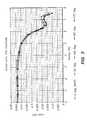
- FIG. 3is a graph of the silicon loss across a flat electrode.
- the present inventionprovides an improved upper electrode system with a multi-part electrode in which a central portion of the electrode having high wear is replaceable independent of an outer peripheral portion of the electrode.
- the upper electrodecan be used in plasma processing systems for processing semiconductor substrates, such as by etching or CVD.
- the multi-part upper electrode systemis particularly useful for large size wafer processing chambers, such as 300 mm wafer processing chambers for which monolithic electrodes are unavailable or costly.
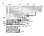
- FIG. 2illustrates a portion of a plasma processing system 100 having an improved upper electrode system allowing replacement of a portion of the upper electrode.
- a central electrode element 110is mounted on a backing plate 112 by a thermally and electrically conductive elastomer.
- a plurality of segmented electrodes 114form a ring around the central electrode 110 and are also mounted to a backing plate 116 .
- the electrode backing plates 112 , 116are secured to a top plate 118 in a removable manner.
- a processed gasis delivered through a channel 122 in the top plate 118 to a plurality of channels 124 above the backing plate 112 .
- the process gasis delivered to the wafer processing chamber through a plurality of perforations 128 in the electrode 110 and backing plate 112 which are in the form of a showerhead electrode.
- a sealing ring 120is provided between the top plate 118 , and the backing plates 112 , 116 to prevent gas flow from the channels 124 into the annulus between the central electrode 110 and the electrode segments 114 .
- the sealing ring 120is provided with O-rings 130 in annular channels in the sealing ring to provide a gas tight seal.
- a step 140is provided in the electrode segments 114 which has been designed to provide etch rate uniformity at the edge of the wafer W.
- the step 140is substantially aligned above an edge of a bottom electrode 150 and is positioned just outside the edge of the wafer W.
- the electrode segments 114may include any number of segments for example, 3 to 10 segments can be used.
- the electrodes 110 , 114are secured to the top plate 118 by threaded screws 134 , 136 extending from the back side of the top plate and into the backing plates 112 , 116 .
- the threaded screws 134 , 136allow the independent removal of the central electrode 110 and the electrode segments 114 when required. Since the wear of the central electrode 110 is estimated to be two to three times the rate of wear on the electrode segments 114 the central electrode can be removed and replaced more often than the outer electrode segments.
- FIG. 3illustrates the etch rate or silicon loss of a silicon upper electrode having a flat shape at different diameters of the electrode.
- the loss or rate of etching of the silicon electrodedecreases significantly at a radius of between 5′′ and 6.5′′ from the center of the electrode. Accordingly, it can be seen that a portion of the electrode outside of about 6.5′′ in diameter can be replaced less frequently than the central portion of the electrode.
- Examples of materials which may be used for the central electrode 110 and the surrounding electrode segments 114include SiC, SiN, AlN, and Al 2 O 3 .
- One particularly preferred material for the electrodes 110 and 114has been found to be silicon since it introduces no additional unwanted elements into the reaction and erodes smoothly creating very few particles. Either single crystal silicon or poly crystalline silicon may be used.
- the backing plates 112 and 116 to which the electrodes 110 and 114 are securedshould be chemically compatible with the process gas, match the coefficient of thermal expansion of the electrodes, be electrically and thermally conductive, and have sufficient mechanical strength to allow fastening to the conductive top plate 118 .
- Examples of materials which can be suitable for use as the top platesinclude graphite and SiC.
- the top plate 118should be formed of a material which is chemically compatible with the process gas, is electrically and thermally conductive, and has sufficient mechanical strength to support the backing plates and the electrodes.
- a material which is chemically compatible with the process gasis electrically and thermally conductive, and has sufficient mechanical strength to support the backing plates and the electrodes.
- One example of the material for the top plateis aluminum.
- the sealing ring 120can be formed from aluminum SiC, silicon, graphite, or quartz, or other materials which are acceptable for use in a plasma processing system.
- a support membersuch as an aluminum mesh can be provided between the electrodes and the backing plates to assure stable electrical and thermal contact over the lifetime of the electrode.
- the electrode segments 114may each be fixed to an independent segment of backing plate 116 or all of the electrode segments 114 can be bonded onto a single backing ring allowing the electrode segments 114 to be removed together in a single step.
- One example of a configuration for the plasma processing system 100 of FIG. 2includes a central electrode element 110 cut from a 12′′ single crystal silicon boule.
- the central electrode element 110has a thickness of about 0.25′′ and an entirely planar lower surface. This diameter is much less expensive to manufacture than a 15′′ single crystal silicon electrode due to the large commercial production of 12′′ single crystal silicon boules for production of 300 mm wafers.
- the outer segmented portion of the electrodeis fabricated from single crystal silicon segments which can be cut from 12′′ diameter single crystal silicon and bonded to a ring-shaped graphite backing plate 116 .
- electrode segmentsare bonded to a ring-shaped graphite backing plate 116 with the electrode segments 114 having a thickness of about 0.5′′ and an angled step 140 ground at an angle of about 45 from the thickness of 0.5′′ down to a thickness of 0.25′′ at the inner diameter of the segments.
- the electrode segments 114together form a ring having an inner diameter of about 12′′ and an outer diameter of about 17′′.
- the sealing ring 120is a quartz ring with elastomeric O-rings and the top plate 118 is formed of Aluminum.
- the joint between the central electrode 110 and the electrode segments 114is positioned at about 5′′ to about 61 ⁇ 2′′ from a center of the electrode, preferably at a radius of about 6′′. Putting the break between the inner and outer parts of the electrode at about 6′′ will allow replacement of the more highly wearing central electrode element 110 independent of the electrode segments 114 .
- the outer electrode segments 114should experience 2-3 times the life of the central electrode 110 reducing costs of electrode replacement.
- the placement of the joint radially inward of the step 140also allows the use of a central electrode 110 having a smaller thickness and thus further reduces costs.
Landscapes
- Engineering & Computer Science (AREA)
- Physics & Mathematics (AREA)
- Plasma & Fusion (AREA)
- Chemical & Material Sciences (AREA)
- Analytical Chemistry (AREA)
- General Physics & Mathematics (AREA)
- Condensed Matter Physics & Semiconductors (AREA)
- Manufacturing & Machinery (AREA)
- Computer Hardware Design (AREA)
- Microelectronics & Electronic Packaging (AREA)
- Power Engineering (AREA)
- Drying Of Semiconductors (AREA)
- Chemical Vapour Deposition (AREA)
- Plasma Technology (AREA)
Abstract
Description
- This application claims priority to U.S. Provisional Patent Application Serial No. 60/383,164 filed May 23, 2002, which is incorporated herein by reference in its entirety.[0001]
- 1. Field of the Invention[0002]
- The invention relates to a multi-part upper electrode for a semiconductor processing plasma reactor and a method of replacing an eroded portion of the multi-part upper electrode.[0003]
- 2. Description of the Related Art[0004]
- Electrodes used in plasma processing reactors for processing semiconductor substrates such as silicon wafers are disclosed in U.S. Pat. Nos. 5,074,456 and 5,569,356, the disclosures of which are hereby incorporated by reference.[0005]
- Dry plasma etching, reactive ion etching, and ion milling techniques were developed in order to overcome numerous limitations associated with chemical etching of semiconductor wafers. Plasma etching, in particular, allows the vertical etch rate to be made much greater than the horizontal etch rate so that the resulting aspect ratio (i.e., the height to width ratio of the resulting notch) of the etched features can be adequately controlled. In fact, plasma etching enables very fine features with high aspect ratios to be formed in films over 1 micrometer in thickness.[0006]
- During the plasma etching process, a plasma is formed above the masked surface of the wafer by adding large amounts of energy to a gas at relatively low pressure, resulting in ionizing the gas. By adjusting the electrical potential of the substrate to be etched, charged species in the plasma can be directed to impinge substantially normally upon the wafer, wherein materials in the unmasked regions of the wafer are removed.[0007]
- The etching process can often be made more effective by using gases that are chemically reactive with the material being etched. So called “reactive ion etching” combines the energetic etching effects of the plasma with the chemical etching effect of the gas. However, many chemically active agents have been found to cause excessive electrode wear.[0008]
- It is desirable to evenly distribute the plasma over the surface of the wafer in order to obtain uniform etching rates over the entire surface of the wafer. For example, U.S. Pat. Nos. 4,595,484, 4,792,378, 4,820,371, 4,960,468 disclose showerhead electrodes for distributing gas through a number of holes in the electrodes. These patents generally describe gas distribution plates having an arrangement of apertures tailored to provide a uniform flow of gas vapors to a semiconductor wafer.[0009]
- A reactive ion etching system typically consists of an etching chamber with an upper electrode or grounded electrode and a lower electrode or RF electrode positioned therein. The wafer to be etched is covered by a suitable mask and placed directly on the RF electrode. The wafer is negatively biased as a result of its interaction with the plasma. A chemically reactive gas such as CF[0010]4, CHF3, CClF3, and SF6or mixtures thereof with O, N2, He, or Ar is introduced into the etching chamber and maintained at a pressure which is typically in the millitorr range. The grounded electrode is provided with gas holes which permit the gas to be uniformly dispersed through the electrode into the chamber. The electric field established between the grounded electrode and the RF electrode will dissociate the reactive gas forming a plasma. The surface of the wafer is etched by chemical interaction with the active ions and by momentum transfer of the ions striking the surface of the wafer. The electric field created by the electrodes will attract the ions to the wafer, causing the ions to strike the surface in a predominantly vertical direction so that the process produces well-defined vertically etched side walls.
- The exposed surfaces of the upper electrode are also etched during wafer processing. Electrode loss or etching results in a need to periodically replace the upper electrode. Thus, it would be desirable to make electrode replacement simple and economical.[0011]
- As substrate size increases it is important to ensure uniform etching and deposition with increasingly large wafer sizes and correspondingly large electrode sizes. The industry move from 200 mm to 300 mm wafers allows manufacturers to double their wafer area and chip output. The increase in wafer size results in certain difficulties in scaling up of the wafer processing tools. For example, single crystal silicon boules used to make some upper electrodes are manufactured in sizes up to 15 inches in diameter. The larger diameter single crystal silicon electrodes are difficult to manufacture with the desired low impurity levels. Thus, the large diameter single crystal silicon electrodes are costly.[0012]
- An[0013]
upper showerhead electrode 10 and a smallerlower electrode 12 for a single wafer etch chamber are shown in FIG. 1. The configuration of FIG. 1 shows an electrode configuration for a capacitively coupled, confined plasma etch chamber with one electrode powered by two RF sources at different frequencies and the other electrode grounded. Thelower electrode 12 is a flat electrode on which a wafer W is supported. Thelower electrode 12 is spaced 1 to 2 cm below theupper electrode 10. In this configuration, theupper electrode 10 has astep 14 ground into the electrode providing an electrode with a thinner inner portion, an angled step portion, and a thicker outer perimeter. Thestep 14 has been designed to provide etch rate uniformity at the edge of the chip. - The[0014]
electrode 10 has a diameter of 15″ to accommodate 300 mm wafers. Anextension 16 of theelectrode 10 is provided which extends the electrode from 15″ to 17″ and is constructed of a plurality of silicon segments. This configuration requires a singlecrystal silicon electrode 10 having a diameter of 15″ which is then ground to form thestep 14. Thislarge diameter electrode 10 is quite costly and requires periodic replacement due to wear. - The present invention relates to a multi-part upper electrode for a semiconductor processing reactor with a replaceable portion and a method of replacing a portion of the electrode.[0015]
- In one embodiment, a multi-part electrode for a plasma reaction chamber includes an electrode top plate and an electrode connected to the top plate. The electrode includes a central silicon element and a plurality of silicon segments surrounding the central silicon element. The central silicon element is removable from the top plate independent of the silicon segments.[0016]
- In another embodiment, a plasma processing system includes a plasma processing chamber, a substrate support within the plasma processing chamber, an RF energy source, a lower electrode, and an upper electrode. The upper electrode includes an electrode top plate, central electrode element secured to the top plate, and a plurality of electrode segments secured to the top plate surrounding the central electrode element. The electrode segments can be formed of the same material as the central electrode element and a joint between the electrode segments and the central electrode is positioned where erosion of the electrode drops from high wear to low wear.[0017]
- In another embodiment, a multi-part electrode for a plasma reaction chamber includes an electrode top plate and an electrode connected to the top plate. The electrode includes a central electrode element having a diameter of about 13 inches or less and a plurality of electrode segments surrounding the central electrode element to create a total electrode diameter of at least 16 inches. The central electrode element is removable from the top plate independent of the electrode segments.[0018]
- In a further embodiment, a method of replacing a portion of an electrode in a plasma reaction chamber, includes the steps of providing an upper electrode in a plasma processing chamber, removing the central electrode from the top plate when it becomes eroded, and replacing the central electrode with a new central electrode. The upper electrode comprising a central electrode element and a plurality of electrode segments surrounding the central electrode element. The central electrode and the electrode segments are independently secured to a top plate of the electrode.[0019]
- The invention will now be described in greater detail with reference to the preferred embodiments illustrated in the accompanying drawings, in which like elements bear like reference numerals, and wherein:[0020]
- FIG. 1 is a side cross sectional view of a portion of upper and lower electrodes in a prior art wafer processing chamber.[0021]
- FIG. 2 is a side cross sectional view of a portion of a wafer processing chamber having a multi-part electrode with a replaceable central electrode element.[0022]
- FIG. 3 is a graph of the silicon loss across a flat electrode.[0023]
- The present invention provides an improved upper electrode system with a multi-part electrode in which a central portion of the electrode having high wear is replaceable independent of an outer peripheral portion of the electrode. The upper electrode can be used in plasma processing systems for processing semiconductor substrates, such as by etching or CVD. The multi-part upper electrode system is particularly useful for large size wafer processing chambers, such as 300 mm wafer processing chambers for which monolithic electrodes are unavailable or costly.[0024]
- FIG. 2 illustrates a portion of a[0025]
plasma processing system 100 having an improved upper electrode system allowing replacement of a portion of the upper electrode. As shown in FIG. 2, acentral electrode element 110 is mounted on abacking plate 112 by a thermally and electrically conductive elastomer. A plurality ofsegmented electrodes 114 form a ring around thecentral electrode 110 and are also mounted to abacking plate 116. Theelectrode backing plates top plate 118 in a removable manner. A processed gas is delivered through achannel 122 in thetop plate 118 to a plurality ofchannels 124 above thebacking plate 112. The process gas is delivered to the wafer processing chamber through a plurality ofperforations 128 in theelectrode 110 andbacking plate 112 which are in the form of a showerhead electrode. - A[0026]
sealing ring 120 is provided between thetop plate 118, and thebacking plates channels 124 into the annulus between thecentral electrode 110 and theelectrode segments 114. The sealingring 120 is provided with O-rings 130 in annular channels in the sealing ring to provide a gas tight seal. - A[0027]
step 140 is provided in theelectrode segments 114 which has been designed to provide etch rate uniformity at the edge of the wafer W. Thestep 140 is substantially aligned above an edge of abottom electrode 150 and is positioned just outside the edge of the wafer W. - The[0028]
electrode segments 114 may include any number of segments for example, 3 to 10 segments can be used. - The[0029]
electrodes top plate 118 by threadedscrews backing plates central electrode 110 and theelectrode segments 114 when required. Since the wear of thecentral electrode 110 is estimated to be two to three times the rate of wear on theelectrode segments 114 the central electrode can be removed and replaced more often than the outer electrode segments. - FIG. 3 illustrates the etch rate or silicon loss of a silicon upper electrode having a flat shape at different diameters of the electrode. As can be seen in FIG. 3, the loss or rate of etching of the silicon electrode decreases significantly at a radius of between 5″ and 6.5″ from the center of the electrode. Accordingly, it can be seen that a portion of the electrode outside of about 6.5″ in diameter can be replaced less frequently than the central portion of the electrode.[0030]
- Examples of materials which may be used for the[0031]
central electrode 110 and the surroundingelectrode segments 114 include SiC, SiN, AlN, and Al2O3. One particularly preferred material for theelectrodes - The[0032]
backing plates electrodes top plate 118. Examples of materials which can be suitable for use as the top plates include graphite and SiC. - The[0033]
top plate 118 should be formed of a material which is chemically compatible with the process gas, is electrically and thermally conductive, and has sufficient mechanical strength to support the backing plates and the electrodes. One example of the material for the top plate is aluminum. - The[0034]
sealing ring 120 can be formed from aluminum SiC, silicon, graphite, or quartz, or other materials which are acceptable for use in a plasma processing system. - In addition to the bonding of the[0035]
electrodes corresponding backing plates - The[0036]
electrode segments 114 may each be fixed to an independent segment ofbacking plate 116 or all of theelectrode segments 114 can be bonded onto a single backing ring allowing theelectrode segments 114 to be removed together in a single step. - One example of a configuration for the[0037]
plasma processing system 100 of FIG. 2 includes acentral electrode element 110 cut from a 12″ single crystal silicon boule. Thecentral electrode element 110 has a thickness of about 0.25″ and an entirely planar lower surface. This diameter is much less expensive to manufacture than a 15″ single crystal silicon electrode due to the large commercial production of 12″ single crystal silicon boules for production of 300 mm wafers. The outer segmented portion of the electrode is fabricated from single crystal silicon segments which can be cut from 12″ diameter single crystal silicon and bonded to a ring-shapedgraphite backing plate 116. In this example, six electrode segments are bonded to a ring-shapedgraphite backing plate 116 with theelectrode segments 114 having a thickness of about 0.5″ and anangled step 140 ground at an angle of about 45 from the thickness of 0.5″ down to a thickness of 0.25″ at the inner diameter of the segments. Theelectrode segments 114 together form a ring having an inner diameter of about 12″ and an outer diameter of about 17″. The sealingring 120 is a quartz ring with elastomeric O-rings and thetop plate 118 is formed of Aluminum. - In the 300 mm wafer processing system described in the above example (with a flat electrode), it has been shown that erosion of the silicon upper electrode drops sharply at a radius of about 5″ to about 6.5″ (see FIG. 3). Accordingly, the joint between the[0038]
central electrode 110 and theelectrode segments 114 is positioned at about 5″ to about 6½″ from a center of the electrode, preferably at a radius of about 6″. Putting the break between the inner and outer parts of the electrode at about 6″ will allow replacement of the more highly wearingcentral electrode element 110 independent of theelectrode segments 114. Theouter electrode segments 114 should experience 2-3 times the life of thecentral electrode 110 reducing costs of electrode replacement. The placement of the joint radially inward of thestep 140 also allows the use of acentral electrode 110 having a smaller thickness and thus further reduces costs. - While the invention has been described in detail with reference to the preferred embodiments thereof, it will be apparent to one skilled in the art that various changes and modifications can be made and equivalents employed, without departing from the present invention.[0039]
Claims (30)
Priority Applications (2)
| Application Number | Priority Date | Filing Date | Title |
|---|---|---|---|
| US10/445,146US7861667B2 (en) | 2002-05-23 | 2003-05-23 | Multi-part electrode for a semiconductor processing plasma reactor and method of replacing a portion of a multi-part electrode |
| US12/954,060US8573153B2 (en) | 2002-05-23 | 2010-11-24 | Multi-part electrode for a semiconductor processing plasma reactor and method of replacing a portion of a multi-part electrode |
Applications Claiming Priority (2)
| Application Number | Priority Date | Filing Date | Title |
|---|---|---|---|
| US38316402P | 2002-05-23 | 2002-05-23 | |
| US10/445,146US7861667B2 (en) | 2002-05-23 | 2003-05-23 | Multi-part electrode for a semiconductor processing plasma reactor and method of replacing a portion of a multi-part electrode |
Related Child Applications (1)
| Application Number | Title | Priority Date | Filing Date |
|---|---|---|---|
| US12/954,060DivisionUS8573153B2 (en) | 2002-05-23 | 2010-11-24 | Multi-part electrode for a semiconductor processing plasma reactor and method of replacing a portion of a multi-part electrode |
Publications (2)
| Publication Number | Publication Date |
|---|---|
| US20040074609A1true US20040074609A1 (en) | 2004-04-22 |
| US7861667B2 US7861667B2 (en) | 2011-01-04 |
Family
ID=29584516
Family Applications (2)
| Application Number | Title | Priority Date | Filing Date |
|---|---|---|---|
| US10/445,146Active2027-09-04US7861667B2 (en) | 2002-05-23 | 2003-05-23 | Multi-part electrode for a semiconductor processing plasma reactor and method of replacing a portion of a multi-part electrode |
| US12/954,060Expired - LifetimeUS8573153B2 (en) | 2002-05-23 | 2010-11-24 | Multi-part electrode for a semiconductor processing plasma reactor and method of replacing a portion of a multi-part electrode |
Family Applications After (1)
| Application Number | Title | Priority Date | Filing Date |
|---|---|---|---|
| US12/954,060Expired - LifetimeUS8573153B2 (en) | 2002-05-23 | 2010-11-24 | Multi-part electrode for a semiconductor processing plasma reactor and method of replacing a portion of a multi-part electrode |
Country Status (7)
| Country | Link |
|---|---|
| US (2) | US7861667B2 (en) |
| EP (1) | EP1512164B1 (en) |
| JP (2) | JP4847009B2 (en) |
| KR (1) | KR101075046B1 (en) |
| CN (1) | CN100442429C (en) |
| AU (1) | AU2003233655A1 (en) |
| WO (1) | WO2003100817A1 (en) |
Cited By (31)
| Publication number | Priority date | Publication date | Assignee | Title |
|---|---|---|---|---|
| US20050241765A1 (en)* | 2004-04-30 | 2005-11-03 | Rajinder Dhindsa | Apparatus including showerhead electrode and heater for plasma processing |
| US20070137573A1 (en)* | 2005-12-21 | 2007-06-21 | Arnold Kholodenko | Apparatus for an optimized plasma chamber grounded electrode assembly |
| US20070187038A1 (en)* | 2006-02-13 | 2007-08-16 | Daxing Ren | Sealed elastomer bonded Si electrodes and the like for reduced particle contamination in dielectric etch |
| US20080178805A1 (en)* | 2006-12-05 | 2008-07-31 | Applied Materials, Inc. | Mid-chamber gas distribution plate, tuned plasma flow control grid and electrode |
| US20080242085A1 (en)* | 2007-03-30 | 2008-10-02 | Lam Research Corporation | Showerhead electrodes and showerhead electrode assemblies having low-particle performance for semiconductor material processing apparatuses |
| US7543547B1 (en)* | 2002-07-31 | 2009-06-09 | Lam Research Corporation | Electrode assembly for plasma processing apparatus |
| US20090163034A1 (en)* | 2007-12-19 | 2009-06-25 | Lam Research Corporation | Composite showerhead electrode assembly for a plasma processing apparatus |
| US20090165717A1 (en)* | 2007-12-31 | 2009-07-02 | Jusung Engineering Co., Ltd | Gas injection unit and thin film deposition apparatus having the same |
| US20100000683A1 (en)* | 2008-07-07 | 2010-01-07 | Lam Research Corporation | Showerhead electrode |
| US20100003824A1 (en)* | 2008-07-07 | 2010-01-07 | Lam Research Corporation | Clamped showerhead electrode assembly |
| US20100006081A1 (en)* | 2007-02-22 | 2010-01-14 | Hana Silicon, Inc | Method for manufacturing silicon matter for plasma processing apparatus |
| US20100101494A1 (en)* | 2008-10-28 | 2010-04-29 | Hsieh Jui Hai Harry | Electrode and chemical vapor deposition apparatus employing the electrode |
| WO2010068849A1 (en)* | 2008-12-12 | 2010-06-17 | Gtsp Global | High temperature and high voltage electrode assembly design |
| US20100175831A1 (en)* | 2009-01-14 | 2010-07-15 | Tokyo Electron Limited | Inductively coupled plasma processing apparatus |
| US20100184298A1 (en)* | 2008-08-15 | 2010-07-22 | Lam Research Corporation | Composite showerhead electrode assembly for a plasma processing apparatus |
| US20100252197A1 (en)* | 2009-04-07 | 2010-10-07 | Lam Reseach Corporation | Showerhead electrode with centering feature |
| US20110039414A1 (en)* | 2008-03-19 | 2011-02-17 | Sanyo Electric Co.,Ltd. | Plasma processing method and plasma processing apparatus |
| US20110070740A1 (en)* | 2009-09-18 | 2011-03-24 | Lam Research Corporation | Clamped monolithic showerhead electrode |
| US20110083809A1 (en)* | 2009-10-13 | 2011-04-14 | Lam Research Corporation | Edge-clamped and mechanically fastened inner electrode of showerhead electrode assembly |
| WO2011092276A1 (en)* | 2010-02-01 | 2011-08-04 | G+R Technology Group Ag | Electrode for a reactor for producing polycrystalline silicon |
| US20110259524A1 (en)* | 2005-03-31 | 2011-10-27 | Naoki Matsumoto | Capacitive coupling plasma processing apparatus and method for using the same |
| US8221582B2 (en) | 2008-07-07 | 2012-07-17 | Lam Research Corporation | Clamped monolithic showerhead electrode |
| US8272346B2 (en) | 2009-04-10 | 2012-09-25 | Lam Research Corporation | Gasket with positioning feature for clamped monolithic showerhead electrode |
| US8313610B2 (en) | 2007-09-25 | 2012-11-20 | Lam Research Corporation | Temperature control modules for showerhead electrode assemblies for plasma processing apparatuses |
| US20130014895A1 (en)* | 2011-07-08 | 2013-01-17 | Tokyo Electron Limited | Substrate processing apparatus |
| US8573152B2 (en) | 2010-09-03 | 2013-11-05 | Lam Research Corporation | Showerhead electrode |
| WO2014116489A1 (en)* | 2013-01-25 | 2014-07-31 | Applied Materials, Inc. | Showerhead having a detachable gas distribution plate |
| US20140238608A1 (en)* | 2013-02-28 | 2014-08-28 | Novellus Systems, Inc. | Ceramic showerhead with embedded rf electrode for capacitively coupled plasma reactor |
| US20150024582A1 (en)* | 2013-02-13 | 2015-01-22 | Lam Research Corporation | Method of making a gas distribution member for a plasma processing chamber |
| US10224182B2 (en) | 2011-10-17 | 2019-03-05 | Novellus Systems, Inc. | Mechanical suppression of parasitic plasma in substrate processing chamber |
| US11396702B2 (en)* | 2016-11-15 | 2022-07-26 | Asm Ip Holding B.V. | Gas supply unit and substrate processing apparatus including the gas supply unit |
Families Citing this family (13)
| Publication number | Priority date | Publication date | Assignee | Title |
|---|---|---|---|---|
| CN100442429C (en) | 2002-05-23 | 2008-12-10 | 蓝姆研究公司 | Multipart electrode for semiconductor processing plasma reactor and method of replacing a part of multipart electrode |
| JP4963842B2 (en)* | 2006-02-13 | 2012-06-27 | 東京エレクトロン株式会社 | Substrate processing chamber cleaning method, storage medium, and substrate processing apparatus |
| US7854820B2 (en)* | 2006-10-16 | 2010-12-21 | Lam Research Corporation | Upper electrode backing member with particle reducing features |
| US7875824B2 (en)* | 2006-10-16 | 2011-01-25 | Lam Research Corporation | Quartz guard ring centering features |
| US7482550B2 (en)* | 2006-10-16 | 2009-01-27 | Lam Research Corporation | Quartz guard ring |
| KR100917475B1 (en)* | 2007-07-06 | 2009-09-14 | 홍인표 | Evaporator with Shower Head |
| WO2009078923A2 (en) | 2007-12-19 | 2009-06-25 | Lam Research Corporation | Film adhesive for semiconductor vacuum processing apparatus |
| TWI501704B (en)* | 2008-02-08 | 2015-09-21 | Lam Res Corp | Methods and apparatus for changing area ratio in a plasma processing system |
| US8869741B2 (en)* | 2008-12-19 | 2014-10-28 | Lam Research Corporation | Methods and apparatus for dual confinement and ultra-high pressure in an adjustable gap plasma chamber |
| JP5528764B2 (en)* | 2009-10-08 | 2014-06-25 | 安斎 聡 | Plasma generator |
| KR102230521B1 (en)* | 2014-08-25 | 2021-03-23 | 주성엔지니어링(주) | Substrate processing apparatus |
| US10256003B2 (en)* | 2017-01-31 | 2019-04-09 | Plansee Japan Ltd. | Blind-vented electrode |
| WO2023238750A1 (en)* | 2022-06-06 | 2023-12-14 | 東京エレクトロン株式会社 | Structure inside plasma processing device, electrode palte, and plasma processing device |
Citations (34)
| Publication number | Priority date | Publication date | Assignee | Title |
|---|---|---|---|---|
| US4230515A (en)* | 1978-07-27 | 1980-10-28 | Davis & Wilder, Inc. | Plasma etching apparatus |
| US4297162A (en)* | 1979-10-17 | 1981-10-27 | Texas Instruments Incorporated | Plasma etching using improved electrode |
| US4340462A (en)* | 1981-02-13 | 1982-07-20 | Lam Research Corporation | Adjustable electrode plasma processing chamber |
| US4579618A (en)* | 1984-01-06 | 1986-04-01 | Tegal Corporation | Plasma reactor apparatus |
| US4595484A (en)* | 1985-12-02 | 1986-06-17 | International Business Machines Corporation | Reactive ion etching apparatus |
| US4610774A (en)* | 1984-11-14 | 1986-09-09 | Hitachi, Ltd. | Target for sputtering |
| US4767641A (en)* | 1986-03-04 | 1988-08-30 | Leybold-Heraeus Gmbh | Plasma treatment apparatus |
| US4792378A (en)* | 1987-12-15 | 1988-12-20 | Texas Instruments Incorporated | Gas dispersion disk for use in plasma enhanced chemical vapor deposition reactor |
| US4820371A (en)* | 1987-12-15 | 1989-04-11 | Texas Instruments Incorporated | Apertured ring for exhausting plasma reactor gases |
| US4885074A (en)* | 1987-02-24 | 1989-12-05 | International Business Machines Corporation | Plasma reactor having segmented electrodes |
| US4960488A (en)* | 1986-12-19 | 1990-10-02 | Applied Materials, Inc. | Reactor chamber self-cleaning process |
| US4979467A (en)* | 1988-05-06 | 1990-12-25 | Fujitsu Limited | Thin film formation apparatus |
| US5074456A (en)* | 1990-09-18 | 1991-12-24 | Lam Research Corporation | Composite electrode for plasma processes |
| US5273588A (en)* | 1992-06-15 | 1993-12-28 | Materials Research Corporation | Semiconductor wafer processing CVD reactor apparatus comprising contoured electrode gas directing means |
| US5298103A (en)* | 1993-07-15 | 1994-03-29 | Hughes Aircraft Company | Electrode assembly useful in confined plasma assisted chemical etching |
| US5422139A (en)* | 1990-04-12 | 1995-06-06 | Balzers Aktiengesellschaft | Method for a reactive surface treatment of a workpiece and a treatment chamber for practicing such method |
| US5472565A (en)* | 1993-11-17 | 1995-12-05 | Lam Research Corporation | Topology induced plasma enhancement for etched uniformity improvement |
| US5522934A (en)* | 1994-04-26 | 1996-06-04 | Tokyo Electron Limited | Plasma processing apparatus using vertical gas inlets one on top of another |
| US5569356A (en)* | 1995-05-19 | 1996-10-29 | Lam Research Corporation | Electrode clamping assembly and method for assembly and use thereof |
| US5571366A (en)* | 1993-10-20 | 1996-11-05 | Tokyo Electron Limited | Plasma processing apparatus |
| US5593540A (en)* | 1992-10-19 | 1997-01-14 | Hitachi, Ltd. | Plasma etching system and plasma etching method |
| US5643394A (en)* | 1994-09-16 | 1997-07-01 | Applied Materials, Inc. | Gas injection slit nozzle for a plasma process reactor |
| US5716485A (en)* | 1995-06-07 | 1998-02-10 | Varian Associates, Inc. | Electrode designs for controlling uniformity profiles in plasma processing reactors |
| US5746875A (en)* | 1994-09-16 | 1998-05-05 | Applied Materials, Inc. | Gas injection slit nozzle for a plasma process reactor |
| US5779803A (en)* | 1993-12-24 | 1998-07-14 | Tokyo Electron Limited | Plasma processing apparatus |
| US6010636A (en)* | 1995-12-29 | 2000-01-04 | Lam Research Corporation | Electrode with domes for plasma focusing |
| US6074518A (en)* | 1994-04-20 | 2000-06-13 | Tokyo Electron Limited | Plasma processing apparatus |
| US6073577A (en)* | 1998-06-30 | 2000-06-13 | Lam Research Corporation | Electrode for plasma processes and method for manufacture and use thereof |
| US6220202B1 (en)* | 1994-06-03 | 2001-04-24 | Tokyo Electron Limited | Apparatus for producing thin films by low temperature plasma-enhanced chemical vapor deposition |
| US6230651B1 (en)* | 1998-12-30 | 2001-05-15 | Lam Research Corporation | Gas injection system for plasma processing |
| US6308654B1 (en)* | 1996-10-18 | 2001-10-30 | Applied Materials, Inc. | Inductively coupled parallel-plate plasma reactor with a conical dome |
| US20020127853A1 (en)* | 2000-12-29 | 2002-09-12 | Hubacek Jerome S. | Electrode for plasma processes and method for manufacture and use thereof |
| US6547921B2 (en)* | 1998-11-30 | 2003-04-15 | Kawasaki Microelectronics, Inc. | Method and apparatus for processing semiconductor substrates |
| US6806653B2 (en)* | 2002-01-31 | 2004-10-19 | Tokyo Electron Limited | Method and structure to segment RF coupling to silicon electrode |
Family Cites Families (28)
| Publication number | Priority date | Publication date | Assignee | Title |
|---|---|---|---|---|
| JPH06291064A (en) | 1993-04-01 | 1994-10-18 | Kokusai Electric Co Ltd | Plasma treatment device |
| US5744049A (en) | 1994-07-18 | 1998-04-28 | Applied Materials, Inc. | Plasma reactor with enhanced plasma uniformity by gas addition, and method of using same |
| JPH08274069A (en)* | 1995-03-30 | 1996-10-18 | Sumitomo Sitix Corp | Silicon electrode device for plasma etching equipment |
| JPH1064831A (en) | 1996-08-20 | 1998-03-06 | Fujitsu Ltd | Vapor phase growth equipment |
| JPH10289881A (en)* | 1997-04-15 | 1998-10-27 | Kokusai Electric Co Ltd | Plasma CVD equipment |
| TW432578B (en)* | 1997-09-18 | 2001-05-01 | Tokyo Electron Ltd | A vacuum processing apparatus |
| JP3480271B2 (en)* | 1997-10-07 | 2003-12-15 | 東京エレクトロン株式会社 | Shower head structure of heat treatment equipment |
| JPH11162940A (en) | 1997-11-28 | 1999-06-18 | Hitachi Chem Co Ltd | Plasma etching electrode |
| DE69929271T2 (en)* | 1998-10-26 | 2006-09-21 | Matsushita Electric Works, Ltd., Kadoma | Apparatus and method for plasma treatment |
| JP2000164568A (en) | 1998-11-25 | 2000-06-16 | Hitachi Chem Co Ltd | Manufacture of plasma etching electrode |
| US6173673B1 (en)* | 1999-03-31 | 2001-01-16 | Tokyo Electron Limited | Method and apparatus for insulating a high power RF electrode through which plasma discharge gases are injected into a processing chamber |
| JP3640204B2 (en)* | 1999-04-14 | 2005-04-20 | 株式会社日立製作所 | Plasma processing apparatus and plasma processing method |
| US6972071B1 (en)* | 1999-07-13 | 2005-12-06 | Nordson Corporation | High-speed symmetrical plasma treatment system |
| US6350317B1 (en) | 1999-12-30 | 2002-02-26 | Lam Research Corporation | Linear drive system for use in a plasma processing system |
| KR100626279B1 (en)* | 1999-12-30 | 2006-09-22 | 엘지.필립스 엘시디 주식회사 | Dry Etching Equipment |
| JP2001313286A (en) | 2000-02-24 | 2001-11-09 | Tokyo Electron Ltd | Parallel-plate dry etching apparatus |
| JP2003524895A (en) | 2000-02-25 | 2003-08-19 | 東京エレクトロン株式会社 | Multi-zone RF electrode for capacitive plasma source |
| TW531820B (en) | 2000-05-12 | 2003-05-11 | Tokyo Electron Ltd | Method of adjusting the thickness of an electrode in a plasma processing system |
| JP4656697B2 (en)* | 2000-06-16 | 2011-03-23 | キヤノンアネルバ株式会社 | High frequency sputtering equipment |
| WO2002007184A2 (en) | 2000-07-13 | 2002-01-24 | Tokyo Electron Limited | Adjustable segmented electrode apparatus and method |
| US6412437B1 (en)* | 2000-08-18 | 2002-07-02 | Micron Technology, Inc. | Plasma enhanced chemical vapor deposition reactor and plasma enhanced chemical vapor deposition process |
| JP2002164329A (en)* | 2000-09-14 | 2002-06-07 | Tokyo Electron Ltd | Plasma treatment apparatus |
| US6391787B1 (en)* | 2000-10-13 | 2002-05-21 | Lam Research Corporation | Stepped upper electrode for plasma processing uniformity |
| US6818096B2 (en)* | 2001-04-12 | 2004-11-16 | Michael Barnes | Plasma reactor electrode |
| US20030106644A1 (en)* | 2001-07-19 | 2003-06-12 | Sirkis Murray D. | Electrode apparatus and method for plasma processing |
| US6962644B2 (en)* | 2002-03-18 | 2005-11-08 | Applied Materials, Inc. | Tandem etch chamber plasma processing system |
| JP3868341B2 (en)* | 2002-04-22 | 2007-01-17 | 日清紡績株式会社 | Plasma etching electrode with excellent heat resistance and dry etching apparatus equipped with the same |
| CN100442429C (en) | 2002-05-23 | 2008-12-10 | 蓝姆研究公司 | Multipart electrode for semiconductor processing plasma reactor and method of replacing a part of multipart electrode |
- 2003
- 2003-05-23CNCNB038140659Apatent/CN100442429C/ennot_activeExpired - Lifetime
- 2003-05-23AUAU2003233655Apatent/AU2003233655A1/ennot_activeAbandoned
- 2003-05-23USUS10/445,146patent/US7861667B2/enactiveActive
- 2003-05-23JPJP2004508375Apatent/JP4847009B2/ennot_activeExpired - Lifetime
- 2003-05-23EPEP03729095.4Apatent/EP1512164B1/ennot_activeExpired - Lifetime
- 2003-05-23KRKR1020047018952Apatent/KR101075046B1/ennot_activeExpired - Lifetime
- 2003-05-23WOPCT/US2003/016318patent/WO2003100817A1/enactiveApplication Filing
- 2010
- 2010-11-24USUS12/954,060patent/US8573153B2/ennot_activeExpired - Lifetime
- 2011
- 2011-08-18JPJP2011179198Apatent/JP5405540B2/ennot_activeExpired - Lifetime
Patent Citations (39)
| Publication number | Priority date | Publication date | Assignee | Title |
|---|---|---|---|---|
| US4230515A (en)* | 1978-07-27 | 1980-10-28 | Davis & Wilder, Inc. | Plasma etching apparatus |
| US4297162A (en)* | 1979-10-17 | 1981-10-27 | Texas Instruments Incorporated | Plasma etching using improved electrode |
| US4340462A (en)* | 1981-02-13 | 1982-07-20 | Lam Research Corporation | Adjustable electrode plasma processing chamber |
| US4579618A (en)* | 1984-01-06 | 1986-04-01 | Tegal Corporation | Plasma reactor apparatus |
| US4610774A (en)* | 1984-11-14 | 1986-09-09 | Hitachi, Ltd. | Target for sputtering |
| US4595484A (en)* | 1985-12-02 | 1986-06-17 | International Business Machines Corporation | Reactive ion etching apparatus |
| US4767641A (en)* | 1986-03-04 | 1988-08-30 | Leybold-Heraeus Gmbh | Plasma treatment apparatus |
| US4960488A (en)* | 1986-12-19 | 1990-10-02 | Applied Materials, Inc. | Reactor chamber self-cleaning process |
| US4885074A (en)* | 1987-02-24 | 1989-12-05 | International Business Machines Corporation | Plasma reactor having segmented electrodes |
| US4820371A (en)* | 1987-12-15 | 1989-04-11 | Texas Instruments Incorporated | Apertured ring for exhausting plasma reactor gases |
| US4792378A (en)* | 1987-12-15 | 1988-12-20 | Texas Instruments Incorporated | Gas dispersion disk for use in plasma enhanced chemical vapor deposition reactor |
| US4979467A (en)* | 1988-05-06 | 1990-12-25 | Fujitsu Limited | Thin film formation apparatus |
| US5422139A (en)* | 1990-04-12 | 1995-06-06 | Balzers Aktiengesellschaft | Method for a reactive surface treatment of a workpiece and a treatment chamber for practicing such method |
| US5074456A (en)* | 1990-09-18 | 1991-12-24 | Lam Research Corporation | Composite electrode for plasma processes |
| US5273588A (en)* | 1992-06-15 | 1993-12-28 | Materials Research Corporation | Semiconductor wafer processing CVD reactor apparatus comprising contoured electrode gas directing means |
| US5593540A (en)* | 1992-10-19 | 1997-01-14 | Hitachi, Ltd. | Plasma etching system and plasma etching method |
| US5298103A (en)* | 1993-07-15 | 1994-03-29 | Hughes Aircraft Company | Electrode assembly useful in confined plasma assisted chemical etching |
| US5571366A (en)* | 1993-10-20 | 1996-11-05 | Tokyo Electron Limited | Plasma processing apparatus |
| US5472565A (en)* | 1993-11-17 | 1995-12-05 | Lam Research Corporation | Topology induced plasma enhancement for etched uniformity improvement |
| US5714031A (en)* | 1993-11-17 | 1998-02-03 | Lam Research Corporation | Topology induced plasma enhancement for etched uniformity improvement |
| US5779803A (en)* | 1993-12-24 | 1998-07-14 | Tokyo Electron Limited | Plasma processing apparatus |
| US6074518A (en)* | 1994-04-20 | 2000-06-13 | Tokyo Electron Limited | Plasma processing apparatus |
| US5522934A (en)* | 1994-04-26 | 1996-06-04 | Tokyo Electron Limited | Plasma processing apparatus using vertical gas inlets one on top of another |
| US6220202B1 (en)* | 1994-06-03 | 2001-04-24 | Tokyo Electron Limited | Apparatus for producing thin films by low temperature plasma-enhanced chemical vapor deposition |
| US5746875A (en)* | 1994-09-16 | 1998-05-05 | Applied Materials, Inc. | Gas injection slit nozzle for a plasma process reactor |
| US5643394A (en)* | 1994-09-16 | 1997-07-01 | Applied Materials, Inc. | Gas injection slit nozzle for a plasma process reactor |
| US5569356A (en)* | 1995-05-19 | 1996-10-29 | Lam Research Corporation | Electrode clamping assembly and method for assembly and use thereof |
| US5716485A (en)* | 1995-06-07 | 1998-02-10 | Varian Associates, Inc. | Electrode designs for controlling uniformity profiles in plasma processing reactors |
| US6010636A (en)* | 1995-12-29 | 2000-01-04 | Lam Research Corporation | Electrode with domes for plasma focusing |
| US6308654B1 (en)* | 1996-10-18 | 2001-10-30 | Applied Materials, Inc. | Inductively coupled parallel-plate plasma reactor with a conical dome |
| US6194322B1 (en)* | 1998-06-30 | 2001-02-27 | Lam Research Corporation | Electrode for plasma processes and method for a manufacture and use thereof |
| US6148765A (en)* | 1998-06-30 | 2000-11-21 | Lam Research Corporation | Electrode for plasma processes and method for manufacture and use thereof |
| US20010031557A1 (en)* | 1998-06-30 | 2001-10-18 | John Lilleland | Electrode for plasma processes and method for manufacture and use thereof |
| US6073577A (en)* | 1998-06-30 | 2000-06-13 | Lam Research Corporation | Electrode for plasma processes and method for manufacture and use thereof |
| US6376385B2 (en)* | 1998-06-30 | 2002-04-23 | Lam Research Corporation | Method of manufacturing assembly for plasma reaction chamber and use thereof |
| US6547921B2 (en)* | 1998-11-30 | 2003-04-15 | Kawasaki Microelectronics, Inc. | Method and apparatus for processing semiconductor substrates |
| US6230651B1 (en)* | 1998-12-30 | 2001-05-15 | Lam Research Corporation | Gas injection system for plasma processing |
| US20020127853A1 (en)* | 2000-12-29 | 2002-09-12 | Hubacek Jerome S. | Electrode for plasma processes and method for manufacture and use thereof |
| US6806653B2 (en)* | 2002-01-31 | 2004-10-19 | Tokyo Electron Limited | Method and structure to segment RF coupling to silicon electrode |
Cited By (70)
| Publication number | Priority date | Publication date | Assignee | Title |
|---|---|---|---|---|
| US7543547B1 (en)* | 2002-07-31 | 2009-06-09 | Lam Research Corporation | Electrode assembly for plasma processing apparatus |
| US7827657B2 (en) | 2002-07-31 | 2010-11-09 | Lam Research Corporation | Method of making an electrode assembly for plasma processing apparatus |
| US20090211085A1 (en)* | 2002-07-31 | 2009-08-27 | Lam Research Corporation | Electrode assembly for plasma processing apparatus |
| US8846539B2 (en) | 2004-04-30 | 2014-09-30 | Lam Research Corporation | Apparatus including showerhead electrode and heater for plasma processing |
| US20100151687A1 (en)* | 2004-04-30 | 2010-06-17 | Lam Research Corporation | Apparatus including showerhead electrode and heater for plasma processing |
| US20050241765A1 (en)* | 2004-04-30 | 2005-11-03 | Rajinder Dhindsa | Apparatus including showerhead electrode and heater for plasma processing |
| US7712434B2 (en)* | 2004-04-30 | 2010-05-11 | Lam Research Corporation | Apparatus including showerhead electrode and heater for plasma processing |
| US10529596B2 (en) | 2005-03-31 | 2020-01-07 | Tokyo Electron Limited | Capacitive coupling plasma processing apparatus and method for using the same |
| US20110259524A1 (en)* | 2005-03-31 | 2011-10-27 | Naoki Matsumoto | Capacitive coupling plasma processing apparatus and method for using the same |
| US8506753B2 (en)* | 2005-03-31 | 2013-08-13 | Tokyo Electron Limited | Capacitive coupling plasma processing apparatus and method for using the same |
| US9607866B2 (en) | 2005-03-31 | 2017-03-28 | Tokyo Electron Limited | Capacitive coupling plasma processing apparatus and method for using the same |
| US7743730B2 (en)* | 2005-12-21 | 2010-06-29 | Lam Research Corporation | Apparatus for an optimized plasma chamber grounded electrode assembly |
| WO2007081653A3 (en)* | 2005-12-21 | 2008-08-07 | Lam Res Corp | Apparatus for an optimized plasma chamber grounded electrode assembly |
| US20070137573A1 (en)* | 2005-12-21 | 2007-06-21 | Arnold Kholodenko | Apparatus for an optimized plasma chamber grounded electrode assembly |
| US9111968B2 (en) | 2005-12-21 | 2015-08-18 | Lam Research Corporation | Plasma processing chamber with a grounded electrode assembly |
| US20100263592A1 (en)* | 2005-12-21 | 2010-10-21 | Arnold Kholodenko | Plasma processing chamber with a grounded electrode assembly |
| KR101438242B1 (en)* | 2005-12-21 | 2014-09-04 | 램 리써치 코포레이션 | Apparatus for an optimized plasma chamber grounded electrode assembly |
| TWI412076B (en)* | 2006-02-13 | 2013-10-11 | Lam Res Corp | Sealed elastomer bonded si electrodes and the like for reduced particle contamination in dielectric etch |
| US20070187038A1 (en)* | 2006-02-13 | 2007-08-16 | Daxing Ren | Sealed elastomer bonded Si electrodes and the like for reduced particle contamination in dielectric etch |
| US8789493B2 (en) | 2006-02-13 | 2014-07-29 | Lam Research Corporation | Sealed elastomer bonded Si electrodes and the like for reduced particle contamination in dielectric etch |
| US20080178805A1 (en)* | 2006-12-05 | 2008-07-31 | Applied Materials, Inc. | Mid-chamber gas distribution plate, tuned plasma flow control grid and electrode |
| US20100006081A1 (en)* | 2007-02-22 | 2010-01-14 | Hana Silicon, Inc | Method for manufacturing silicon matter for plasma processing apparatus |
| US8069817B2 (en) | 2007-03-30 | 2011-12-06 | Lam Research Corporation | Showerhead electrodes and showerhead electrode assemblies having low-particle performance for semiconductor material processing apparatuses |
| WO2008121288A1 (en)* | 2007-03-30 | 2008-10-09 | Lam Research Corporation | Showerhead electrodes and showerhead electrode assemblies having low-particle performance for semiconductor material processing apparatuses |
| US8443756B2 (en) | 2007-03-30 | 2013-05-21 | Lam Research Corporation | Showerhead electrodes and showerhead electrode assemblies having low-particle performance for semiconductor material processing apparatuses |
| US20080242085A1 (en)* | 2007-03-30 | 2008-10-02 | Lam Research Corporation | Showerhead electrodes and showerhead electrode assemblies having low-particle performance for semiconductor material processing apparatuses |
| US8313610B2 (en) | 2007-09-25 | 2012-11-20 | Lam Research Corporation | Temperature control modules for showerhead electrode assemblies for plasma processing apparatuses |
| US20090163034A1 (en)* | 2007-12-19 | 2009-06-25 | Lam Research Corporation | Composite showerhead electrode assembly for a plasma processing apparatus |
| US20130244441A1 (en)* | 2007-12-19 | 2013-09-19 | Lam Research Corporation | Composite showerhead electrode assembly for a plasma processing apparatus |
| US8701268B2 (en)* | 2007-12-19 | 2014-04-22 | Lam Research Corporation | Composite showerhead electrode assembly for a plasma processing apparatus |
| US8418649B2 (en)* | 2007-12-19 | 2013-04-16 | Lam Research Corporation | Composite showerhead electrode assembly for a plasma processing apparatus |
| US20090165717A1 (en)* | 2007-12-31 | 2009-07-02 | Jusung Engineering Co., Ltd | Gas injection unit and thin film deposition apparatus having the same |
| US8317922B2 (en)* | 2007-12-31 | 2012-11-27 | Jusung Engnineering Co., Ltd. | Gas injection unit and thin film deposition apparatus having the same |
| US20110039414A1 (en)* | 2008-03-19 | 2011-02-17 | Sanyo Electric Co.,Ltd. | Plasma processing method and plasma processing apparatus |
| US20120171872A1 (en)* | 2008-07-07 | 2012-07-05 | Lam Research Corporation | Clamped showerhead electrode assembly |
| US8221582B2 (en) | 2008-07-07 | 2012-07-17 | Lam Research Corporation | Clamped monolithic showerhead electrode |
| US20100003824A1 (en)* | 2008-07-07 | 2010-01-07 | Lam Research Corporation | Clamped showerhead electrode assembly |
| US8313805B2 (en)* | 2008-07-07 | 2012-11-20 | Lam Research Corporation | Clamped showerhead electrode assembly |
| US8206506B2 (en) | 2008-07-07 | 2012-06-26 | Lam Research Corporation | Showerhead electrode |
| US8161906B2 (en)* | 2008-07-07 | 2012-04-24 | Lam Research Corporation | Clamped showerhead electrode assembly |
| US20100000683A1 (en)* | 2008-07-07 | 2010-01-07 | Lam Research Corporation | Showerhead electrode |
| US8147648B2 (en)* | 2008-08-15 | 2012-04-03 | Lam Research Corporation | Composite showerhead electrode assembly for a plasma processing apparatus |
| US20100184298A1 (en)* | 2008-08-15 | 2010-07-22 | Lam Research Corporation | Composite showerhead electrode assembly for a plasma processing apparatus |
| US20100101494A1 (en)* | 2008-10-28 | 2010-04-29 | Hsieh Jui Hai Harry | Electrode and chemical vapor deposition apparatus employing the electrode |
| WO2010068849A1 (en)* | 2008-12-12 | 2010-06-17 | Gtsp Global | High temperature and high voltage electrode assembly design |
| US20100147219A1 (en)* | 2008-12-12 | 2010-06-17 | Jui Hai Hsieh | High temperature and high voltage electrode assembly design |
| US20100175831A1 (en)* | 2009-01-14 | 2010-07-15 | Tokyo Electron Limited | Inductively coupled plasma processing apparatus |
| US8597463B2 (en) | 2009-01-14 | 2013-12-03 | Tokyo Electron Limited | Inductively coupled plasma processing apparatus |
| US8402918B2 (en) | 2009-04-07 | 2013-03-26 | Lam Research Corporation | Showerhead electrode with centering feature |
| US20100252197A1 (en)* | 2009-04-07 | 2010-10-07 | Lam Reseach Corporation | Showerhead electrode with centering feature |
| US8272346B2 (en) | 2009-04-10 | 2012-09-25 | Lam Research Corporation | Gasket with positioning feature for clamped monolithic showerhead electrode |
| US8419959B2 (en) | 2009-09-18 | 2013-04-16 | Lam Research Corporation | Clamped monolithic showerhead electrode |
| US20110070740A1 (en)* | 2009-09-18 | 2011-03-24 | Lam Research Corporation | Clamped monolithic showerhead electrode |
| US9245716B2 (en) | 2009-10-13 | 2016-01-26 | Lam Research Corporation | Edge-clamped and mechanically fastened inner electrode of showerhead electrode assembly |
| US10262834B2 (en)* | 2009-10-13 | 2019-04-16 | Lam Research Corporation | Edge-clamped and mechanically fastened inner electrode of showerhead electrode assembly |
| US20110083809A1 (en)* | 2009-10-13 | 2011-04-14 | Lam Research Corporation | Edge-clamped and mechanically fastened inner electrode of showerhead electrode assembly |
| WO2011092276A1 (en)* | 2010-02-01 | 2011-08-04 | G+R Technology Group Ag | Electrode for a reactor for producing polycrystalline silicon |
| US8573152B2 (en) | 2010-09-03 | 2013-11-05 | Lam Research Corporation | Showerhead electrode |
| US9460893B2 (en)* | 2011-07-08 | 2016-10-04 | Tokyo Electron Limited | Substrate processing apparatus |
| US20130014895A1 (en)* | 2011-07-08 | 2013-01-17 | Tokyo Electron Limited | Substrate processing apparatus |
| US10224182B2 (en) | 2011-10-17 | 2019-03-05 | Novellus Systems, Inc. | Mechanical suppression of parasitic plasma in substrate processing chamber |
| US11621150B2 (en) | 2011-10-17 | 2023-04-04 | Lam Research Corporation | Mechanical suppression of parasitic plasma in substrate processing chamber |
| WO2014116489A1 (en)* | 2013-01-25 | 2014-07-31 | Applied Materials, Inc. | Showerhead having a detachable gas distribution plate |
| US9610591B2 (en) | 2013-01-25 | 2017-04-04 | Applied Materials, Inc. | Showerhead having a detachable gas distribution plate |
| US10625277B2 (en) | 2013-01-25 | 2020-04-21 | Applied Materials, Inc. | Showerhead having a detachable gas distribution plate |
| US11130142B2 (en) | 2013-01-25 | 2021-09-28 | Applied Materials, Inc. | Showerhead having a detachable gas distribution plate |
| US20150024582A1 (en)* | 2013-02-13 | 2015-01-22 | Lam Research Corporation | Method of making a gas distribution member for a plasma processing chamber |
| US9449795B2 (en)* | 2013-02-28 | 2016-09-20 | Novellus Systems, Inc. | Ceramic showerhead with embedded RF electrode for capacitively coupled plasma reactor |
| US20140238608A1 (en)* | 2013-02-28 | 2014-08-28 | Novellus Systems, Inc. | Ceramic showerhead with embedded rf electrode for capacitively coupled plasma reactor |
| US11396702B2 (en)* | 2016-11-15 | 2022-07-26 | Asm Ip Holding B.V. | Gas supply unit and substrate processing apparatus including the gas supply unit |
Also Published As
| Publication number | Publication date |
|---|---|
| JP2012043796A (en) | 2012-03-01 |
| JP2005527976A (en) | 2005-09-15 |
| JP5405540B2 (en) | 2014-02-05 |
| CN100442429C (en) | 2008-12-10 |
| EP1512164B1 (en) | 2016-01-06 |
| WO2003100817A1 (en) | 2003-12-04 |
| KR20040111691A (en) | 2004-12-31 |
| US8573153B2 (en) | 2013-11-05 |
| US20110067814A1 (en) | 2011-03-24 |
| JP4847009B2 (en) | 2011-12-28 |
| US7861667B2 (en) | 2011-01-04 |
| EP1512164A1 (en) | 2005-03-09 |
| CN1663016A (en) | 2005-08-31 |
| KR101075046B1 (en) | 2011-10-19 |
| AU2003233655A1 (en) | 2003-12-12 |
Similar Documents
| Publication | Publication Date | Title |
|---|---|---|
| US7861667B2 (en) | Multi-part electrode for a semiconductor processing plasma reactor and method of replacing a portion of a multi-part electrode | |
| US7939778B2 (en) | Plasma processing chamber with guard ring for upper electrode assembly | |
| KR101057610B1 (en) | Dielectric material etching method | |
| US9093483B2 (en) | Showerhead electrode assembly with gas flow modification for extended electrode life | |
| US8845855B2 (en) | Electrode for plasma processes and method for manufacture and use thereof | |
| US9111968B2 (en) | Plasma processing chamber with a grounded electrode assembly | |
| EP0826229B1 (en) | Electrode clamping assembly and method for assembly and use thereof | |
| EP1989727B1 (en) | SEALED ELASTOMER BONDED Si ELECTRODES AND THE LIKE FOR REDUCED PARTICLE CONTAMINATION IN DIELECTRIC ETCH | |
| EP0702392B1 (en) | Plasma reactor | |
| KR200476554Y1 (en) | Hot edge ring with sloped upper surface | |
| JP2005527976A5 (en) |
Legal Events
| Date | Code | Title | Description |
|---|---|---|---|
| AS | Assignment | Owner name:LAM RESEARCH CORPORATION, CALIFORNIA Free format text:ASSIGNMENT OF ASSIGNORS INTEREST;ASSIGNORS:FISCHER, ANDREAS;KENNEDY, WILLIAM S.;LOEWENHARDT, PETER;AND OTHERS;REEL/FRAME:014353/0879;SIGNING DATES FROM 20030703 TO 20030710 Owner name:LAM RESEARCH CORPORATION, CALIFORNIA Free format text:ASSIGNMENT OF ASSIGNORS INTEREST;ASSIGNORS:FISCHER, ANDREAS;KENNEDY, WILLIAM S.;LOEWENHARDT, PETER;AND OTHERS;SIGNING DATES FROM 20030703 TO 20030710;REEL/FRAME:014353/0879 | |
| FEPP | Fee payment procedure | Free format text:PAYOR NUMBER ASSIGNED (ORIGINAL EVENT CODE: ASPN); ENTITY STATUS OF PATENT OWNER: LARGE ENTITY | |
| STCF | Information on status: patent grant | Free format text:PATENTED CASE | |
| FPAY | Fee payment | Year of fee payment:4 | |
| MAFP | Maintenance fee payment | Free format text:PAYMENT OF MAINTENANCE FEE, 8TH YEAR, LARGE ENTITY (ORIGINAL EVENT CODE: M1552) Year of fee payment:8 | |
| MAFP | Maintenance fee payment | Free format text:PAYMENT OF MAINTENANCE FEE, 12TH YEAR, LARGE ENTITY (ORIGINAL EVENT CODE: M1553); ENTITY STATUS OF PATENT OWNER: LARGE ENTITY Year of fee payment:12 |