US20040063242A1 - Semiconductor multi-package module having package stacked over ball grid array package and having wire bond interconnect between stacked packages - Google Patents
Semiconductor multi-package module having package stacked over ball grid array package and having wire bond interconnect between stacked packagesDownload PDFInfo
- Publication number
- US20040063242A1 US20040063242A1US10/632,568US63256803AUS2004063242A1US 20040063242 A1US20040063242 A1US 20040063242A1US 63256803 AUS63256803 AUS 63256803AUS 2004063242 A1US2004063242 A1US 2004063242A1
- Authority
- US
- United States
- Prior art keywords
- package
- substrate
- die
- packages
- bga
- Prior art date
- Legal status (The legal status is an assumption and is not a legal conclusion. Google has not performed a legal analysis and makes no representation as to the accuracy of the status listed.)
- Granted
Links
Images


Classifications
- H—ELECTRICITY
- H01—ELECTRIC ELEMENTS
- H01L—SEMICONDUCTOR DEVICES NOT COVERED BY CLASS H10
- H01L23/00—Details of semiconductor or other solid state devices
- H01L23/48—Arrangements for conducting electric current to or from the solid state body in operation, e.g. leads, terminal arrangements ; Selection of materials therefor
- H01L23/488—Arrangements for conducting electric current to or from the solid state body in operation, e.g. leads, terminal arrangements ; Selection of materials therefor consisting of soldered or bonded constructions
- H01L23/498—Leads, i.e. metallisations or lead-frames on insulating substrates, e.g. chip carriers
- H01L23/49833—Leads, i.e. metallisations or lead-frames on insulating substrates, e.g. chip carriers the chip support structure consisting of a plurality of insulating substrates
- H—ELECTRICITY
- H01—ELECTRIC ELEMENTS
- H01L—SEMICONDUCTOR DEVICES NOT COVERED BY CLASS H10
- H01L23/00—Details of semiconductor or other solid state devices
- H01L23/28—Encapsulations, e.g. encapsulating layers, coatings, e.g. for protection
- H01L23/31—Encapsulations, e.g. encapsulating layers, coatings, e.g. for protection characterised by the arrangement or shape
- H01L23/3107—Encapsulations, e.g. encapsulating layers, coatings, e.g. for protection characterised by the arrangement or shape the device being completely enclosed
- H01L23/3121—Encapsulations, e.g. encapsulating layers, coatings, e.g. for protection characterised by the arrangement or shape the device being completely enclosed a substrate forming part of the encapsulation
- H01L23/3128—Encapsulations, e.g. encapsulating layers, coatings, e.g. for protection characterised by the arrangement or shape the device being completely enclosed a substrate forming part of the encapsulation the substrate having spherical bumps for external connection
- H—ELECTRICITY
- H01—ELECTRIC ELEMENTS
- H01L—SEMICONDUCTOR DEVICES NOT COVERED BY CLASS H10
- H01L23/00—Details of semiconductor or other solid state devices
- H01L23/34—Arrangements for cooling, heating, ventilating or temperature compensation ; Temperature sensing arrangements
- H01L23/42—Fillings or auxiliary members in containers or encapsulations selected or arranged to facilitate heating or cooling
- H01L23/433—Auxiliary members in containers characterised by their shape, e.g. pistons
- H01L23/4334—Auxiliary members in encapsulations
- H—ELECTRICITY
- H01—ELECTRIC ELEMENTS
- H01L—SEMICONDUCTOR DEVICES NOT COVERED BY CLASS H10
- H01L23/00—Details of semiconductor or other solid state devices
- H01L23/552—Protection against radiation, e.g. light or electromagnetic waves
- H—ELECTRICITY
- H01—ELECTRIC ELEMENTS
- H01L—SEMICONDUCTOR DEVICES NOT COVERED BY CLASS H10
- H01L25/00—Assemblies consisting of a plurality of semiconductor or other solid state devices
- H01L25/03—Assemblies consisting of a plurality of semiconductor or other solid state devices all the devices being of a type provided for in a single subclass of subclasses H10B, H10D, H10F, H10H, H10K or H10N, e.g. assemblies of rectifier diodes
- H01L25/04—Assemblies consisting of a plurality of semiconductor or other solid state devices all the devices being of a type provided for in a single subclass of subclasses H10B, H10D, H10F, H10H, H10K or H10N, e.g. assemblies of rectifier diodes the devices not having separate containers
- H01L25/065—Assemblies consisting of a plurality of semiconductor or other solid state devices all the devices being of a type provided for in a single subclass of subclasses H10B, H10D, H10F, H10H, H10K or H10N, e.g. assemblies of rectifier diodes the devices not having separate containers the devices being of a type provided for in group H10D89/00
- H01L25/0657—Stacked arrangements of devices
- H—ELECTRICITY
- H01—ELECTRIC ELEMENTS
- H01L—SEMICONDUCTOR DEVICES NOT COVERED BY CLASS H10
- H01L25/00—Assemblies consisting of a plurality of semiconductor or other solid state devices
- H01L25/03—Assemblies consisting of a plurality of semiconductor or other solid state devices all the devices being of a type provided for in a single subclass of subclasses H10B, H10D, H10F, H10H, H10K or H10N, e.g. assemblies of rectifier diodes
- H01L25/10—Assemblies consisting of a plurality of semiconductor or other solid state devices all the devices being of a type provided for in a single subclass of subclasses H10B, H10D, H10F, H10H, H10K or H10N, e.g. assemblies of rectifier diodes the devices having separate containers
- H01L25/105—Assemblies consisting of a plurality of semiconductor or other solid state devices all the devices being of a type provided for in a single subclass of subclasses H10B, H10D, H10F, H10H, H10K or H10N, e.g. assemblies of rectifier diodes the devices having separate containers the devices being integrated devices of class H10
- H—ELECTRICITY
- H01—ELECTRIC ELEMENTS
- H01L—SEMICONDUCTOR DEVICES NOT COVERED BY CLASS H10
- H01L2224/00—Indexing scheme for arrangements for connecting or disconnecting semiconductor or solid-state bodies and methods related thereto as covered by H01L24/00
- H01L2224/01—Means for bonding being attached to, or being formed on, the surface to be connected, e.g. chip-to-package, die-attach, "first-level" interconnects; Manufacturing methods related thereto
- H01L2224/02—Bonding areas; Manufacturing methods related thereto
- H01L2224/04—Structure, shape, material or disposition of the bonding areas prior to the connecting process
- H01L2224/05—Structure, shape, material or disposition of the bonding areas prior to the connecting process of an individual bonding area
- H01L2224/0554—External layer
- H01L2224/05599—Material
- H—ELECTRICITY
- H01—ELECTRIC ELEMENTS
- H01L—SEMICONDUCTOR DEVICES NOT COVERED BY CLASS H10
- H01L2224/00—Indexing scheme for arrangements for connecting or disconnecting semiconductor or solid-state bodies and methods related thereto as covered by H01L24/00
- H01L2224/01—Means for bonding being attached to, or being formed on, the surface to be connected, e.g. chip-to-package, die-attach, "first-level" interconnects; Manufacturing methods related thereto
- H01L2224/10—Bump connectors; Manufacturing methods related thereto
- H01L2224/15—Structure, shape, material or disposition of the bump connectors after the connecting process
- H01L2224/16—Structure, shape, material or disposition of the bump connectors after the connecting process of an individual bump connector
- H01L2224/161—Disposition
- H01L2224/16151—Disposition the bump connector connecting between a semiconductor or solid-state body and an item not being a semiconductor or solid-state body, e.g. chip-to-substrate, chip-to-passive
- H01L2224/16221—Disposition the bump connector connecting between a semiconductor or solid-state body and an item not being a semiconductor or solid-state body, e.g. chip-to-substrate, chip-to-passive the body and the item being stacked
- H01L2224/16225—Disposition the bump connector connecting between a semiconductor or solid-state body and an item not being a semiconductor or solid-state body, e.g. chip-to-substrate, chip-to-passive the body and the item being stacked the item being non-metallic, e.g. insulating substrate with or without metallisation
- H—ELECTRICITY
- H01—ELECTRIC ELEMENTS
- H01L—SEMICONDUCTOR DEVICES NOT COVERED BY CLASS H10
- H01L2224/00—Indexing scheme for arrangements for connecting or disconnecting semiconductor or solid-state bodies and methods related thereto as covered by H01L24/00
- H01L2224/01—Means for bonding being attached to, or being formed on, the surface to be connected, e.g. chip-to-package, die-attach, "first-level" interconnects; Manufacturing methods related thereto
- H01L2224/26—Layer connectors, e.g. plate connectors, solder or adhesive layers; Manufacturing methods related thereto
- H01L2224/31—Structure, shape, material or disposition of the layer connectors after the connecting process
- H01L2224/32—Structure, shape, material or disposition of the layer connectors after the connecting process of an individual layer connector
- H01L2224/321—Disposition
- H01L2224/32151—Disposition the layer connector connecting between a semiconductor or solid-state body and an item not being a semiconductor or solid-state body, e.g. chip-to-substrate, chip-to-passive
- H01L2224/32221—Disposition the layer connector connecting between a semiconductor or solid-state body and an item not being a semiconductor or solid-state body, e.g. chip-to-substrate, chip-to-passive the body and the item being stacked
- H01L2224/32225—Disposition the layer connector connecting between a semiconductor or solid-state body and an item not being a semiconductor or solid-state body, e.g. chip-to-substrate, chip-to-passive the body and the item being stacked the item being non-metallic, e.g. insulating substrate with or without metallisation
- H—ELECTRICITY
- H01—ELECTRIC ELEMENTS
- H01L—SEMICONDUCTOR DEVICES NOT COVERED BY CLASS H10
- H01L2224/00—Indexing scheme for arrangements for connecting or disconnecting semiconductor or solid-state bodies and methods related thereto as covered by H01L24/00
- H01L2224/01—Means for bonding being attached to, or being formed on, the surface to be connected, e.g. chip-to-package, die-attach, "first-level" interconnects; Manufacturing methods related thereto
- H01L2224/42—Wire connectors; Manufacturing methods related thereto
- H01L2224/44—Structure, shape, material or disposition of the wire connectors prior to the connecting process
- H01L2224/45—Structure, shape, material or disposition of the wire connectors prior to the connecting process of an individual wire connector
- H01L2224/45001—Core members of the connector
- H01L2224/45099—Material
- H—ELECTRICITY
- H01—ELECTRIC ELEMENTS
- H01L—SEMICONDUCTOR DEVICES NOT COVERED BY CLASS H10
- H01L2224/00—Indexing scheme for arrangements for connecting or disconnecting semiconductor or solid-state bodies and methods related thereto as covered by H01L24/00
- H01L2224/01—Means for bonding being attached to, or being formed on, the surface to be connected, e.g. chip-to-package, die-attach, "first-level" interconnects; Manufacturing methods related thereto
- H01L2224/42—Wire connectors; Manufacturing methods related thereto
- H01L2224/47—Structure, shape, material or disposition of the wire connectors after the connecting process
- H01L2224/48—Structure, shape, material or disposition of the wire connectors after the connecting process of an individual wire connector
- H01L2224/4805—Shape
- H01L2224/4809—Loop shape
- H01L2224/48091—Arched
- H—ELECTRICITY
- H01—ELECTRIC ELEMENTS
- H01L—SEMICONDUCTOR DEVICES NOT COVERED BY CLASS H10
- H01L2224/00—Indexing scheme for arrangements for connecting or disconnecting semiconductor or solid-state bodies and methods related thereto as covered by H01L24/00
- H01L2224/01—Means for bonding being attached to, or being formed on, the surface to be connected, e.g. chip-to-package, die-attach, "first-level" interconnects; Manufacturing methods related thereto
- H01L2224/42—Wire connectors; Manufacturing methods related thereto
- H01L2224/47—Structure, shape, material or disposition of the wire connectors after the connecting process
- H01L2224/48—Structure, shape, material or disposition of the wire connectors after the connecting process of an individual wire connector
- H01L2224/481—Disposition
- H01L2224/48151—Connecting between a semiconductor or solid-state body and an item not being a semiconductor or solid-state body, e.g. chip-to-substrate, chip-to-passive
- H01L2224/48221—Connecting between a semiconductor or solid-state body and an item not being a semiconductor or solid-state body, e.g. chip-to-substrate, chip-to-passive the body and the item being stacked
- H01L2224/48225—Connecting between a semiconductor or solid-state body and an item not being a semiconductor or solid-state body, e.g. chip-to-substrate, chip-to-passive the body and the item being stacked the item being non-metallic, e.g. insulating substrate with or without metallisation
- H01L2224/48227—Connecting between a semiconductor or solid-state body and an item not being a semiconductor or solid-state body, e.g. chip-to-substrate, chip-to-passive the body and the item being stacked the item being non-metallic, e.g. insulating substrate with or without metallisation connecting the wire to a bond pad of the item
- H—ELECTRICITY
- H01—ELECTRIC ELEMENTS
- H01L—SEMICONDUCTOR DEVICES NOT COVERED BY CLASS H10
- H01L2224/00—Indexing scheme for arrangements for connecting or disconnecting semiconductor or solid-state bodies and methods related thereto as covered by H01L24/00
- H01L2224/01—Means for bonding being attached to, or being formed on, the surface to be connected, e.g. chip-to-package, die-attach, "first-level" interconnects; Manufacturing methods related thereto
- H01L2224/42—Wire connectors; Manufacturing methods related thereto
- H01L2224/47—Structure, shape, material or disposition of the wire connectors after the connecting process
- H01L2224/48—Structure, shape, material or disposition of the wire connectors after the connecting process of an individual wire connector
- H01L2224/484—Connecting portions
- H01L2224/48463—Connecting portions the connecting portion on the bonding area of the semiconductor or solid-state body being a ball bond
- H01L2224/48465—Connecting portions the connecting portion on the bonding area of the semiconductor or solid-state body being a ball bond the other connecting portion not on the bonding area being a wedge bond, i.e. ball-to-wedge, regular stitch
- H—ELECTRICITY
- H01—ELECTRIC ELEMENTS
- H01L—SEMICONDUCTOR DEVICES NOT COVERED BY CLASS H10
- H01L2224/00—Indexing scheme for arrangements for connecting or disconnecting semiconductor or solid-state bodies and methods related thereto as covered by H01L24/00
- H01L2224/73—Means for bonding being of different types provided for in two or more of groups H01L2224/10, H01L2224/18, H01L2224/26, H01L2224/34, H01L2224/42, H01L2224/50, H01L2224/63, H01L2224/71
- H01L2224/732—Location after the connecting process
- H01L2224/73201—Location after the connecting process on the same surface
- H01L2224/73203—Bump and layer connectors
- H01L2224/73204—Bump and layer connectors the bump connector being embedded into the layer connector
- H—ELECTRICITY
- H01—ELECTRIC ELEMENTS
- H01L—SEMICONDUCTOR DEVICES NOT COVERED BY CLASS H10
- H01L2224/00—Indexing scheme for arrangements for connecting or disconnecting semiconductor or solid-state bodies and methods related thereto as covered by H01L24/00
- H01L2224/73—Means for bonding being of different types provided for in two or more of groups H01L2224/10, H01L2224/18, H01L2224/26, H01L2224/34, H01L2224/42, H01L2224/50, H01L2224/63, H01L2224/71
- H01L2224/732—Location after the connecting process
- H01L2224/73251—Location after the connecting process on different surfaces
- H01L2224/73265—Layer and wire connectors
- H—ELECTRICITY
- H01—ELECTRIC ELEMENTS
- H01L—SEMICONDUCTOR DEVICES NOT COVERED BY CLASS H10
- H01L2224/00—Indexing scheme for arrangements for connecting or disconnecting semiconductor or solid-state bodies and methods related thereto as covered by H01L24/00
- H01L2224/80—Methods for connecting semiconductor or other solid state bodies using means for bonding being attached to, or being formed on, the surface to be connected
- H01L2224/85—Methods for connecting semiconductor or other solid state bodies using means for bonding being attached to, or being formed on, the surface to be connected using a wire connector
- H01L2224/8538—Bonding interfaces outside the semiconductor or solid-state body
- H01L2224/85399—Material
- H—ELECTRICITY
- H01—ELECTRIC ELEMENTS
- H01L—SEMICONDUCTOR DEVICES NOT COVERED BY CLASS H10
- H01L2224/00—Indexing scheme for arrangements for connecting or disconnecting semiconductor or solid-state bodies and methods related thereto as covered by H01L24/00
- H01L2224/80—Methods for connecting semiconductor or other solid state bodies using means for bonding being attached to, or being formed on, the surface to be connected
- H01L2224/85—Methods for connecting semiconductor or other solid state bodies using means for bonding being attached to, or being formed on, the surface to be connected using a wire connector
- H01L2224/85909—Post-treatment of the connector or wire bonding area
- H01L2224/8592—Applying permanent coating, e.g. protective coating
- H—ELECTRICITY
- H01—ELECTRIC ELEMENTS
- H01L—SEMICONDUCTOR DEVICES NOT COVERED BY CLASS H10
- H01L2225/00—Details relating to assemblies covered by the group H01L25/00 but not provided for in its subgroups
- H01L2225/03—All the devices being of a type provided for in the same main group of the same subclass of class H10, e.g. assemblies of rectifier diodes
- H01L2225/04—All the devices being of a type provided for in the same main group of the same subclass of class H10, e.g. assemblies of rectifier diodes the devices not having separate containers
- H01L2225/065—All the devices being of a type provided for in the same main group of the same subclass of class H10
- H01L2225/06503—Stacked arrangements of devices
- H01L2225/0651—Wire or wire-like electrical connections from device to substrate
- H—ELECTRICITY
- H01—ELECTRIC ELEMENTS
- H01L—SEMICONDUCTOR DEVICES NOT COVERED BY CLASS H10
- H01L2225/00—Details relating to assemblies covered by the group H01L25/00 but not provided for in its subgroups
- H01L2225/03—All the devices being of a type provided for in the same main group of the same subclass of class H10, e.g. assemblies of rectifier diodes
- H01L2225/04—All the devices being of a type provided for in the same main group of the same subclass of class H10, e.g. assemblies of rectifier diodes the devices not having separate containers
- H01L2225/065—All the devices being of a type provided for in the same main group of the same subclass of class H10
- H01L2225/06503—Stacked arrangements of devices
- H01L2225/06572—Auxiliary carrier between devices, the carrier having an electrical connection structure
- H—ELECTRICITY
- H01—ELECTRIC ELEMENTS
- H01L—SEMICONDUCTOR DEVICES NOT COVERED BY CLASS H10
- H01L2225/00—Details relating to assemblies covered by the group H01L25/00 but not provided for in its subgroups
- H01L2225/03—All the devices being of a type provided for in the same main group of the same subclass of class H10, e.g. assemblies of rectifier diodes
- H01L2225/04—All the devices being of a type provided for in the same main group of the same subclass of class H10, e.g. assemblies of rectifier diodes the devices not having separate containers
- H01L2225/065—All the devices being of a type provided for in the same main group of the same subclass of class H10
- H01L2225/06503—Stacked arrangements of devices
- H01L2225/06589—Thermal management, e.g. cooling
- H—ELECTRICITY
- H01—ELECTRIC ELEMENTS
- H01L—SEMICONDUCTOR DEVICES NOT COVERED BY CLASS H10
- H01L2225/00—Details relating to assemblies covered by the group H01L25/00 but not provided for in its subgroups
- H01L2225/03—All the devices being of a type provided for in the same main group of the same subclass of class H10, e.g. assemblies of rectifier diodes
- H01L2225/10—All the devices being of a type provided for in the same main group of the same subclass of class H10, e.g. assemblies of rectifier diodes the devices having separate containers
- H01L2225/1005—All the devices being of a type provided for in the same main group of the same subclass of class H10, e.g. assemblies of rectifier diodes the devices having separate containers the devices being integrated devices of class H10
- H01L2225/1011—All the devices being of a type provided for in the same main group of the same subclass of class H10, e.g. assemblies of rectifier diodes the devices having separate containers the devices being integrated devices of class H10 the containers being in a stacked arrangement
- H01L2225/1017—All the devices being of a type provided for in the same main group of the same subclass of class H10, e.g. assemblies of rectifier diodes the devices having separate containers the devices being integrated devices of class H10 the containers being in a stacked arrangement the lowermost container comprising a device support
- H01L2225/1023—All the devices being of a type provided for in the same main group of the same subclass of class H10, e.g. assemblies of rectifier diodes the devices having separate containers the devices being integrated devices of class H10 the containers being in a stacked arrangement the lowermost container comprising a device support the support being an insulating substrate
- H—ELECTRICITY
- H01—ELECTRIC ELEMENTS
- H01L—SEMICONDUCTOR DEVICES NOT COVERED BY CLASS H10
- H01L2225/00—Details relating to assemblies covered by the group H01L25/00 but not provided for in its subgroups
- H01L2225/03—All the devices being of a type provided for in the same main group of the same subclass of class H10, e.g. assemblies of rectifier diodes
- H01L2225/10—All the devices being of a type provided for in the same main group of the same subclass of class H10, e.g. assemblies of rectifier diodes the devices having separate containers
- H01L2225/1005—All the devices being of a type provided for in the same main group of the same subclass of class H10, e.g. assemblies of rectifier diodes the devices having separate containers the devices being integrated devices of class H10
- H01L2225/1011—All the devices being of a type provided for in the same main group of the same subclass of class H10, e.g. assemblies of rectifier diodes the devices having separate containers the devices being integrated devices of class H10 the containers being in a stacked arrangement
- H01L2225/1047—Details of electrical connections between containers
- H01L2225/1052—Wire or wire-like electrical connections
- H—ELECTRICITY
- H01—ELECTRIC ELEMENTS
- H01L—SEMICONDUCTOR DEVICES NOT COVERED BY CLASS H10
- H01L2225/00—Details relating to assemblies covered by the group H01L25/00 but not provided for in its subgroups
- H01L2225/03—All the devices being of a type provided for in the same main group of the same subclass of class H10, e.g. assemblies of rectifier diodes
- H01L2225/10—All the devices being of a type provided for in the same main group of the same subclass of class H10, e.g. assemblies of rectifier diodes the devices having separate containers
- H01L2225/1005—All the devices being of a type provided for in the same main group of the same subclass of class H10, e.g. assemblies of rectifier diodes the devices having separate containers the devices being integrated devices of class H10
- H01L2225/1011—All the devices being of a type provided for in the same main group of the same subclass of class H10, e.g. assemblies of rectifier diodes the devices having separate containers the devices being integrated devices of class H10 the containers being in a stacked arrangement
- H01L2225/1094—Thermal management, e.g. cooling
- H—ELECTRICITY
- H01—ELECTRIC ELEMENTS
- H01L—SEMICONDUCTOR DEVICES NOT COVERED BY CLASS H10
- H01L24/00—Arrangements for connecting or disconnecting semiconductor or solid-state bodies; Methods or apparatus related thereto
- H01L24/01—Means for bonding being attached to, or being formed on, the surface to be connected, e.g. chip-to-package, die-attach, "first-level" interconnects; Manufacturing methods related thereto
- H01L24/42—Wire connectors; Manufacturing methods related thereto
- H01L24/47—Structure, shape, material or disposition of the wire connectors after the connecting process
- H01L24/48—Structure, shape, material or disposition of the wire connectors after the connecting process of an individual wire connector
- H—ELECTRICITY
- H01—ELECTRIC ELEMENTS
- H01L—SEMICONDUCTOR DEVICES NOT COVERED BY CLASS H10
- H01L24/00—Arrangements for connecting or disconnecting semiconductor or solid-state bodies; Methods or apparatus related thereto
- H01L24/73—Means for bonding being of different types provided for in two or more of groups H01L24/10, H01L24/18, H01L24/26, H01L24/34, H01L24/42, H01L24/50, H01L24/63, H01L24/71
- H—ELECTRICITY
- H01—ELECTRIC ELEMENTS
- H01L—SEMICONDUCTOR DEVICES NOT COVERED BY CLASS H10
- H01L2924/00—Indexing scheme for arrangements or methods for connecting or disconnecting semiconductor or solid-state bodies as covered by H01L24/00
- H01L2924/0001—Technical content checked by a classifier
- H01L2924/00014—Technical content checked by a classifier the subject-matter covered by the group, the symbol of which is combined with the symbol of this group, being disclosed without further technical details
- H—ELECTRICITY
- H01—ELECTRIC ELEMENTS
- H01L—SEMICONDUCTOR DEVICES NOT COVERED BY CLASS H10
- H01L2924/00—Indexing scheme for arrangements or methods for connecting or disconnecting semiconductor or solid-state bodies as covered by H01L24/00
- H01L2924/01—Chemical elements
- H01L2924/01029—Copper [Cu]
- H—ELECTRICITY
- H01—ELECTRIC ELEMENTS
- H01L—SEMICONDUCTOR DEVICES NOT COVERED BY CLASS H10
- H01L2924/00—Indexing scheme for arrangements or methods for connecting or disconnecting semiconductor or solid-state bodies as covered by H01L24/00
- H01L2924/01—Chemical elements
- H01L2924/01079—Gold [Au]
- H—ELECTRICITY
- H01—ELECTRIC ELEMENTS
- H01L—SEMICONDUCTOR DEVICES NOT COVERED BY CLASS H10
- H01L2924/00—Indexing scheme for arrangements or methods for connecting or disconnecting semiconductor or solid-state bodies as covered by H01L24/00
- H01L2924/10—Details of semiconductor or other solid state devices to be connected
- H01L2924/11—Device type
- H01L2924/12—Passive devices, e.g. 2 terminal devices
- H01L2924/1204—Optical Diode
- H01L2924/12042—LASER
- H—ELECTRICITY
- H01—ELECTRIC ELEMENTS
- H01L—SEMICONDUCTOR DEVICES NOT COVERED BY CLASS H10
- H01L2924/00—Indexing scheme for arrangements or methods for connecting or disconnecting semiconductor or solid-state bodies as covered by H01L24/00
- H01L2924/15—Details of package parts other than the semiconductor or other solid state devices to be connected
- H01L2924/151—Die mounting substrate
- H01L2924/153—Connection portion
- H01L2924/1531—Connection portion the connection portion being formed only on the surface of the substrate opposite to the die mounting surface
- H01L2924/15311—Connection portion the connection portion being formed only on the surface of the substrate opposite to the die mounting surface being a ball array, e.g. BGA
- H—ELECTRICITY
- H01—ELECTRIC ELEMENTS
- H01L—SEMICONDUCTOR DEVICES NOT COVERED BY CLASS H10
- H01L2924/00—Indexing scheme for arrangements or methods for connecting or disconnecting semiconductor or solid-state bodies as covered by H01L24/00
- H01L2924/15—Details of package parts other than the semiconductor or other solid state devices to be connected
- H01L2924/151—Die mounting substrate
- H01L2924/153—Connection portion
- H01L2924/1532—Connection portion the connection portion being formed on the die mounting surface of the substrate
- H01L2924/1533—Connection portion the connection portion being formed on the die mounting surface of the substrate the connection portion being formed both on the die mounting surface of the substrate and outside the die mounting surface of the substrate
- H01L2924/15331—Connection portion the connection portion being formed on the die mounting surface of the substrate the connection portion being formed both on the die mounting surface of the substrate and outside the die mounting surface of the substrate being a ball array, e.g. BGA
- H—ELECTRICITY
- H01—ELECTRIC ELEMENTS
- H01L—SEMICONDUCTOR DEVICES NOT COVERED BY CLASS H10
- H01L2924/00—Indexing scheme for arrangements or methods for connecting or disconnecting semiconductor or solid-state bodies as covered by H01L24/00
- H01L2924/15—Details of package parts other than the semiconductor or other solid state devices to be connected
- H01L2924/161—Cap
- H01L2924/1615—Shape
- H01L2924/16152—Cap comprising a cavity for hosting the device, e.g. U-shaped cap
- H—ELECTRICITY
- H01—ELECTRIC ELEMENTS
- H01L—SEMICONDUCTOR DEVICES NOT COVERED BY CLASS H10
- H01L2924/00—Indexing scheme for arrangements or methods for connecting or disconnecting semiconductor or solid-state bodies as covered by H01L24/00
- H01L2924/15—Details of package parts other than the semiconductor or other solid state devices to be connected
- H01L2924/181—Encapsulation
- H—ELECTRICITY
- H01—ELECTRIC ELEMENTS
- H01L—SEMICONDUCTOR DEVICES NOT COVERED BY CLASS H10
- H01L2924/00—Indexing scheme for arrangements or methods for connecting or disconnecting semiconductor or solid-state bodies as covered by H01L24/00
- H01L2924/19—Details of hybrid assemblies other than the semiconductor or other solid state devices to be connected
- H01L2924/191—Disposition
- H01L2924/19101—Disposition of discrete passive components
- H01L2924/19107—Disposition of discrete passive components off-chip wires
- H—ELECTRICITY
- H01—ELECTRIC ELEMENTS
- H01L—SEMICONDUCTOR DEVICES NOT COVERED BY CLASS H10
- H01L2924/00—Indexing scheme for arrangements or methods for connecting or disconnecting semiconductor or solid-state bodies as covered by H01L24/00
- H01L2924/30—Technical effects
- H01L2924/301—Electrical effects
- H01L2924/3025—Electromagnetic shielding
Definitions
- This inventionrelates to semiconductor packaging.
- Portable electronic productssuch as mobile phones, mobile computing, and various consumer products require higher semiconductor functionality and performance in a limited footprint and minimal thickness and weight at the lowest cost. This has driven the industry to increase integration on the individual semiconductor chips.
- the primary practical limitation to the number of chips that can be stacked in a stacked die packageis the low final test yield of the stacked-die package. It is inevitable that some of the die in the package will be defective to some extent, and therefore the final package test yield will be the product of the individual die test yields, each of which is always less than 100%. This can be particularly a problem even if only two die are stacked in a package but one of them has low yield because of design complexity or technology.
- a further limitationis electromagnetic interference between the stacked die, particularly between RF and digital die, because there is no electrical shielding of either die.
- Another approach to integrating on the “z-axis”is to stack die packages to form a multi-package module. Stacked packages can provide numerous advantages as compared to stacked-die packages.
- each package with its diecan be electrically tested, and rejected unless it shows satisfactory performance, before the packages are stacked. As a result the final stacked multi-package module yields are maximized.
- More efficient coolingcan be provided in stacked packages, by inserting a heat spreader between the packages in the stack as well as at the top of the module.
- Package stackingallows electromagnetic shielding of the RF die and avoids interference with other die in the module.
- Each die or more than one diecan be packaged in a respective package in the stack using the most efficient first level interconnect technology for the chip type and configuration, such as wire bonding or flip chip, to maximize performance and minimize cost.
- the z-interconnect between packages in a stacked multi-package moduleis a critical technology from the standpoint of manufacturability, design flexibility and cost.
- Z-interconnectsthat have been proposed include peripheral solder ball connection, and flexible substrate folded over the top of the bottom package.
- peripheral solder balls for z-interconnects in stacked multi-package moduleslimits the number of connections that can be made and limits design flexibility, and results in a thicker and higher cost package.
- a flexible folding substrateprovides in principle for design flexibility, there is no established manufacturing infrastructure for the folding process.
- the use of a flexible folding substraterequires a two metal layer flex substrate, and these are expensive.
- the folded flexible substrate approachis restricted to low pincount applications because of limits in routing the circuitry in two metal layer substrates.
- FIG. 1is a diagrammatic sketch in a sectional view illustrating the structure of a standard Ball Grid Array (“BGA”) package, well established in the industry, that can be used as a bottom package in a stacked multi-package module (“MPM”).
- the BGAshown generally at 10 , includes a die 14 attached onto a substrate 12 having at least one metal layer. Any of various substrate types may be used, including for example: a laminate with 2-6 metal layers, or a build up substrate with 4-8 metal layers, or a flexible polyimide tape with 1-2 metal layers, or a ceramic multilayer substrate.
- the die 1has two metal layers 121 , 123 , each patterned to provide appropriate circuitry and connected by way of vias 122 .
- the dieis conventionally attached to a surface of the substrate using an adhesive, typically referred to as the die attach epoxy, shown at 13 in FIG. 1 and, in the configuration in FIG. 1, the surface of the substrate onto which the die is attached may be referred to as the “upper” surface, and the metal layer on that surface may be referred to as the “upper” metal layer, although the die attach surface need not have any particular orientation in use.
- the dieis wire bonded onto wire bond sites on the upper metal layer of the substrate to establish electrical connections.
- the die 14 and the wire bonds 16are encapsulated with a molding compound. 17 that provides protection from ambient and from mechanical stress to facilitate handling operations, and provides a surface for marking for identification.
- Solder balls 18are reflowed onto bonding pads on the lower metal layer of the substrate to provide interconnection to the motherboard (not shown in the FIGS.) of a final product, such as a computer.
- Solder masks 125 , 127are patterned over the metal layers 121 , 123 to expose the underlying metal at bonding sites for electrical connection, for example the wire bond sites and bonding pads for bonding the wire bonds 16 and solder balls 18 .
- FIG. 2is a diagrammatic sketch in a sectional view illustrating the structure of an example of a 2-stack MPM, generally at 20 , in which the z-interconnect between the packages in the stack is made by way of solder balls.
- a first package(which may be referred to as the “bottom” package) is similar to a standard BGA as shown in FIG. 1 (and similar reference numerals are employed to point to similar features of the bottom package in FIGS. 1 and 2).
- a second package(which may be referred to as the “top” package) is stacked on the bottom package and is similar in structure to the bottom package, except that the solder balls in the top package are arranged at the periphery of the top package substrate, so that they effect the z-interconnect without interference with the encapsulation of the bottom BGA.
- the top package in FIG. 2includes a die 24 attached onto a substrate 22 having at least one metal layer.
- the top package substrate 22 shown by way of example in FIG. 2has two metal layers 221 , 223 , each patterned to provide appropriate circuitry and connected by way of vias 222 .
- the dieis conventionally attached to a surface of the substrate (the “upper” surface) using an adhesive, typically referred to as the die attach epoxy, shown at 23 in FIG. 2.
- the dieis wire bonded onto wire bond sites on the upper metal layer of the substrate to establish electrical connections.
- the top package die 24 and wire bonds 26are encapsulated with a top package molding compound 27 .
- Solder balls 28are reflowed onto bonding pads located on the peripheral margin of the lower metal layer of the top package substrate to provide z-interconnection to the bottom package.
- Solder masks 225 , 227are patterned over the metal layers 221 , 223 to expose the underlying metal at bonding sites for electrical connection, for example the wire bond sites and bonding pads for bonding the wire bonds 26 and solder balls 28 .
- the z-interconnection in the MPM of FIG. 2is achieved by reflowing the solder balls 28 attached to peripheral bonding pads on the lower metal layer of the top package substrate onto peripheral bonding pads on the upper metal layer of the bottom BGA.
- the distance h between the top and bottom packagesmust be at least as great as the encapsulation height of the bottom package, which may be 0.3 mm or more, and typically is in a range between 0.5 mm and 1.5 mm.
- the solder balls 28must accordingly be of a sufficiently large diameter that when they are reflowed they make good contact with the bonding pads of the bottom BGA; that is, the solder ball 28 diameter must be greater than the encapsulation height.
- a larger ball diameterdictates a larger ball pitch that in turn limits the number of balls that can be fitted in the available space.
- the peripheral arrangement of the solder ballsforces the bottom BGA to be significantly larger than the mold cap of a standard BGA.
- the package body sizeis 1.7 mm larger than the die.
- the body sizeis about 2 mm larger than the mold cap.
- the top package substratemust have at least 2 metal layers to facilitate the electrical connections.
- FIG. 3is a diagrammatic sketch in a sectional view illustrating the structure of an example of a known 2-stack flip chip MPM, shown generally at 30 .
- the bottom BGA flip chip packageincludes a substrate 32 having a patterned metal layer 31 onto which the die 34 is connected by flip chip bumps 36 , such as solder bumps, gold stud bumps or anisotropically conducting film or paste.
- the flip chip bumpsare affixed to a patterned array of bump pads on the active surface of the die and, as the active surface of the die faces downward in relation to an upward-facing patterned metal layer of the substrate, such an arrangement may be referred to as a “die down”, flip chip package.
- a polymer underfill 33 between die and substrateprovides protection from ambient and adds mechanical integrity to the structure.
- Such a flip chip packagein which the substrate has a metal layer on only the upper surface, is connected to the underlying circuitry (such as a motherboard, not shown in the FIG.) by solder balls 38 connected to the metal layer through solder vias 35 .
- the top BGA in this configurationis similar to the bottom BGA, except that the top BGA has z-interconnect solder balls 338 connected (through solder vias 335 in the top substrate) to the metal layer 331 only at the periphery of the top substrate. Solder balls 338 are reflowed onto the metal layer 31 of the bottom substrate to provide the z-interconnect.
- the top BGA in this configurationincludes a substrate 332 having a patterned metal layer 331 onto which the top BGA die 334 is connected by flip chip bumps 336 . Between the top BGA die and substrate is a polymer underfill 333 .
- a structure as in FIG. 3is more appropriate for high electrical performance applications, but it has similar limitations to configurations of the type shown in of FIG. 2. It presents an improvement over the FIG. 2 configuration in that the bottom BGA has no molding, allowing for use of smaller diameter (h) solder balls at the periphery of the top BGA for connection between the packages.
- FIG. 4is a diagrammatic sketch in a sectional view illustrating the structure of an example of a known 2-stack folded flexible substrate MPM, shown generally at 40 .
- the bottom package in the configuration of FIG. 4has a 2-metal layer flexible substrate onto which the die is bonded via small beams to the first metal layer of the substrate.
- the second metal layer of the bottom package substratecarries the solder balls for connection to the underlying circuitry, such as a motherboard (not shown).
- the substrateis large enough to be folded over the top of the package, thus bringing the electrical interconnect lines upward where they are available for connection to the top package (an example of which is described below) by way of an array of solder balls on the top package.
- the space around the die and between the die and folded-over substrateis encapsulated to provide protection and rigidity.
- the two-metal layer bottom package substrate 42includes a first metal layer 141 and a second metal layer 143 , each patterned to provide appropriate circuitry and connected by way of vias 142 .
- a part of the first metal layer, over a part of the bottom substrate,is processed (for example, using an array of punches) to present an array of cantilever beams or tabs 46 arranged to correspond to an array of interconnect pads on the active surface of the bottom package die 44 .
- the first metal layer 141faces upwardly.
- the dieis aligned, active surface downward, over the die attach part of the substrate, and the cantilevers and the corresponding interconnect pads are joined, typically for example by a “thermosonic” process employing a combination of pressure, heat, and ultrasonic energy to complete the electrical connections.
- the die 44is affixed using an adhesive 43 , typically a die attach epoxy, onto the die attach part of the flexible substrate 42 .
- a second metal layer 143 of the bottom package substrate 42faces downwardly in the die attach part of the substrate.
- Solder balls 48are reflowed onto bonding pads located on an array on the downward-facing part of the second metal layer 143 to provide for interconnection of the MPM to underlying circuitry (not shown).
- a solder mask 147is patterned over the second metal layer 143 to expose the underlying metal as bonding sites for electrical connection, including the bond pads for connection with the underlying circuitry by way of solder balls 48 , and the bond pads for connection with the top package by way of solder balls 18 , as described below.
- the top packageis generally similar to the BGA of FIG. 1, in which the die is wire bonded onto wire bond sites on the upper metal layer of the substrate to establish electrical connections.
- the top package die 14is attached onto a substrate 12 having (in this example) two metal layers 121 , 123 , each patterned to provide appropriate circuitry and connected by way of vias 122 .
- the dieis conventionally attached to the upper surface of the top package substrate using an adhesive 13 , typically a die attach epoxy.
- the die 14 and the wire bonds 16are encapsulated with a molding compound 17 that provides protection from ambient and from mechanical stress to facilitate handling operations, and provides a surface for marking for identification.
- Solder balls 18are reflowed onto bonding pads 143 on the upward-facing metal layer of the folded-over bottom package substrate to provide z-interconnection between the top and the bottom packages.
- An advantage of a structure as in FIG. 4is that the folded-over substrate provides sufficient area on the upward-facing surface of the folded-over bottom package substrate to accommodate a full array of solder balls in the top package and to accommodate more complex interconnect between the two packages. It also provides for a small package footprint.
- a primary disadvantage of this configurationis the high cost of the substrate and the unavailability of folding technology and equipment.
- a common feature of all these stacked package configurationsis that they enable pretesting of each package, and provide for production MPMs with higher final test yields.
- This inventionis directed to multi-package modules having stacked packages.
- z-interconnection between the stacked packages in the MPMis wire bond based.
- the inventionfeatures various configurations of various stacked packages, and methods for stacking and interconnecting the various packages by wire-bonding based z-interconnection.
- the package stackcan include any of a variety of BGA packages and/or any of a variety of Land Grid Array (“LGA”) packages; the package stack can include wire bonded and/or flip chip packages; the package stack can include a thermal enhancement feature enabled by one or more heat spreaders in or on the stack; the package stack can include one or more packages having a flip chip die bonded either to the top or to the bottom of the BGA or LGA; the package stack can include one or more BGA and/or LGA packages having more than one die in the package stacked or side by side; the stack can include electromagnetic shield for one or more of the packages; and the stack can include any substrate, laminate or build-up or flexible or ceramic, provided that the z-interconnect pads are made available for bonding on the periphery of the packages.
- LGALand Grid Array
- the inventionfeatures a multi-package module having stacked lower and upper packages, each package including a die attached to a substrate, in which the upper and lower substrates are interconnected by wire bonding.
- the inventionprovides for excellent manufacturability, high design flexibility, and low cost to produce a stacked package module having a low profile and a small footprint.
- the wire bond z-interconnectis well established in the industry; it is the lowest cost interconnect technique and it is directly applicable, without significant modification, to the stacked multi-package modules of the invention. It provides design flexibility to the relative size of the BGA to LGA that can be bridged by wire length. Using available techniques and equipment the wire in a wire bond can be as short as 0.5 mm or as long as 5 mm.
- the arrangement of the z-interconnect padscan be implemented through either or both BGA and LGA substrate designs.
- z-interconnectcan be formed between pads that are not precisely aligned over one another, by employing so-called “out of sequence bonding” that is in current use in the industry.
- the wire bonding pitchis the finest available technology in the industry at 50 microns currently, and projected to go to 25 microns. This enables a high number of z-interconnects. Both manufacturability and design flexibility contribute to the low cost of the MPM.
- a minimum footprint for a typical BGA or LGAis 1.7 mm larger than the die size.
- the addition of the z-interconnect bond pads according to the inventionwill increase the BGA size minimally, by 0.8 mm.
- a typical BGA thicknessis 1.0 mm and LGA thickness is 0.8 mm.
- Atypical adhesive thicknesscan be in the range 0.025 mm to 0.100 mm. Both the footprint and the thickness of the stacked package MPM according to the invention fall within accepted ranges for most applications.
- the multi-package moduleincludes three or more packages, affixed serially to form a stack.
- the inventionfeatures a multi-package module having stacked first (“bottom”) and second (“top”) packages, each package including a die attached to a substrate and connected to the substrate by wire bonding, in which the top package substrate and the bottom package substrate are interconnected by wire bonding.
- each packageis fully encapsulated with a molding material; in other embodiments at least one of the packages is encapsulated only to an extent sufficient to protect the wire bonds between the die and the substrate during subsequent handling and testing.
- the second packageis an LGA package, and in some such embodiments the LGA package substrate is a single-metal layer substrate.
- the inventionfeatures a multi-package module having stacked first (“bottom”) and second (“top”) packages, the bottom package being a BGA package, each package including a die attached to a substrate, in which the top package substrate and the BGA package substrate are interconnected by wire bonding.
- the inventionfeatures a multi-package module having stacked packages in which at least one package is provided with an electrical shield.
- the electrical shieldmay additionally be configured to serve as a heat spreader.
- the package that is provided with an electrical shieldincludes an RF die, and the shield serves to limit electromagnetic interference between the RF die and other die in the multi-package module.
- the bottom packageis provided with an electrical shield.
- the inventionfeatures methods for making multi-package modules, by providing a first (bottom) package including at least one die on a first (bottom) package substrate, placing over the first package a second (top) package including at least one die on a second (top) package substrate, and forming wire bond z-interconnects between the first and second (top and bottom) substrates.
- the packagescan be tested prior to assembly, and packages not meeting requirements for performance or reliability can be discarded, so that preferably only first packages and second packages tested as “good” are used in the assembled module.
- the inventionfeatures a method for making a multi-package module including a LGA package stacked over a BGA package, in which the top and bottom packages are electrically interconnected by wire bonding.
- a BGA packageis provided, usually in an unsingulated strip of molded BGA packages; preferably the BGA packages in the strip are tested for performance and reliability and packages identified as “good” are subjected to subsequent treatment; adhesive is dispensed over the upper surface of the molding on “good” BGA packages; a singulated molded land grid array package is provided; preferably the LGA package is tested and identified as “good”; the “good” LGA package is placed onto the adhesive over the molding on the “good” BGA package, and the adhesive is cured; optionally and preferably a plasma clean operation is performed followed by formation of wire bond z-interconnections between the stacked top LGA and bottom BGA package; optionally and preferably an additional plasma clean may be performed, followed by the formation of the MPM molding. Further steps
- the LGA (top) packageis fully molded, providing a generally planar upper surface of the LGA package; in other embodiments the wire bonds but not the entire upper die surface of the LGA package is molded, molding of the LGA being carried out by dispensing the molding compound only around the periphery of the die and the margin of the LGA package substrate
- the inventionfeatures a method for making a multi-package module including a LGA package stacked over a BGA package, in which the top and bottom packages are electrically interconnected by wire bonding, and in which the bottom package is provided with an electromagnetic shield.
- a ball grid array packageis provided, usually in an unsingulated strip of BGA packages; the BGA packages are provided with shields affixed over the die; preferably the BGA packages in the strip are tested for performance and reliability and packages identified as “good” are subjected to subsequent treatment; adhesive is dispensed over the upper surface of the shields on “good” BGA packages; a singulated molded land grid array package is provided; preferably the LGA package is tested and identified as “good”; the “good” LGA package is placed onto the adhesive over the shield, and the adhesive is cured; optionally and preferably a plasma clean operation is performed followed by formation of wire bond z-interconnections between the stacked top LGA and bottom BGA package; optionally and preferably an additional plasma clean may be performed, followed by the formation of the MPM molding. Further steps include attachment of second-level interconnect solder balls to the underside of the module; testing and singulation of the completed module from the strip, for example by saw singulation or by punch singulation; and packaging
- the methodincludes steps for providing the multi-package module with a heat spreader.
- a similar processis performed, with additional steps interposed installation of supported heat spreader by a “drop-in” mold operation, or for installation of a simple planar heat spreader by a drop-in mold operation; or by applying adhesive onto an upper surface of the top package molding or onto an upper surface of a spacer upon the top package, and affixing the planar heat spreader onto the adhesive.
- two or more first molded packagesare provided in an unsingulated strip, and assembly of the two or more modules proceeds on the strip, and singulation of the two or more modules is carried out after assembly has been completed.
- the electrical connections between the stacked packagesemploys conventional wire bonding to form the z-interconnect between upper and lower package substrates in the stack.
- Particular advantagesinclude the use of established manufacturing infrastructure, low production cost, design flexibility, and a thin package product.
- the z-interconnect wire bondingcan be carried out, in the various package and module configurations, by drawing the wire to a conductive pad on the first package substrate from a bump formed on a conductive pad on the second package substrate; or, by drawing the wire to a conductive pad on the second package substrate from a bump formed on a conductive pad on the first package substrate.
- the inventionprovides for assembly of more than one semiconductor in a thin and minimal footprint package at the lowest cost and highest final test yield. Furthermore some stack configurations according to the invention allow for high thermal performance, high electrical performance or electrical isolation of an RF component from a digital one. Other stack configurations provide a very thin structure appropriate for handheld or consumer products. All provide for a method for assembly that allows individual testing of the stacked packages to maximize the final yield of the module.
- Additional process stepswill be employed to complete the multi-package module according to the invention. For example, it may be preferred not to attach solder balls for connection of the lowermost package in the stack to the motherboard until the final step before singulation of the MPMs. And, for example, a plasma clean may be performed at any of a variety of points in the process, such as following adhesive cure and prior to encapsulation, and such as prior to and/or following z-interconnect wire bonding.
- the individual packagescan be provided as strips of several packages, connected in a row for ease of handling during manufacture, and the multi-package modules are singulated following completion of process steps.
- the package stackscan be formed on a strip of nonsingulated first packages of a selected type by affixing singulated second packages and forming the wire bonded z-interconnects until the process of forming the modules is complete, and then singulating the modules.
- MPM according to the inventioncan be used for building computers, telecommunications equipment, and consumer and industrial electronics devices.
- FIG. 1is a diagrammatic sketch in a sectional view thru a conventional ball grid array semiconductor package.
- FIG. 2is a diagrammatic sketch in a sectional view thru a conventional multi-package module having solder ball z-interconnection between stacked ball grid array semiconductor packages.
- FIG. 3is a diagrammatic sketch in a sectional view thru a conventional flip chip multi-package module having solder ball z-interconnection between stacked flip chip semiconductor packages.
- FIG. 4is a diagrammatic sketch in a sectional view thru a conventional multi-package module having a folded flexible substrate and solder ball z-interconnection between stacked semiconductor packages.
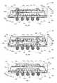
- FIG. 5Ais a diagrammatic sketch in a sectional view thru an embodiment of a multi-package module having wire bond z-interconnection between stacked BGA and LGA semiconductor packages according to an aspect of the invention.
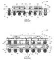
- FIG. 5Bis a diagrammatic sketch in a plan view showing a bottom BGA substrate having z-interconnect bond pads in an arrangement suitable for use in an embodiment of the invention as shown in FIG. 5A.
- FIG. 5Cis a diagrammatic sketch in a plan view showing a top LGA substrate having z-interconnect bond pads in an arrangement suitable for use in an embodiment of the invention as shown in FIG. 5A.
- FIG. 5Dis a diagrammatic sketch in a sectional view thru an embodiment of a multi-package module having wire bond z-interconnection between stacked BGA and LGA semiconductor packages according to an aspect of the invention, and having a heat spreader affixed to an upper surface of the top package.
- FIG. 5Eis a diagrammatic sketch in a sectional view thru an embodiment of a multi-package module having wire bond z-interconnection between stacked BGA and LGA semiconductor packages, and having a heat spreader according to another aspect of the invention.
- FIG. 6Ais a diagrammatic sketch in a sectional view thru another embodiment of a multi-package module having wire bond z-interconnection between stacked BGA and LGA semiconductor packages according to an aspect of the invention, in which the top package is provided with peripheral molding.
- FIG. 6Bis a diagrammatic sketch in a sectional view thru another embodiment of a multi-package module having wire bond z-interconnection between stacked BGA and LGA semiconductor packages according to an aspect of the invention, in which the top package is provided with peripheral molding, and the module is provided with a heat spreader.
- FIG. 7is a diagrammatic sketch in a sectional view thru another embodiment of a multi-package module having wire bond z-interconnection between stacked BGA and LGA semiconductor packages according to an aspect of the invention, in which the top package substrate has a one metal layer substrate.
- FIG. 8Ais a diagrammatic sketch in a sectional view thru an embodiment of a multi-package module having wire bond z-interconnection between stacked BGA and LGA semiconductor packages according to a further aspect of the invention, in which an electrical shield is provided on the bottom package.
- FIG. 8Bis a diagrammatic sketch in a sectional view thru another embodiment of a multi-package module having wire bond z-interconnection between stacked BGA and LGA semiconductor packages according to an aspect of the invention, in which an electrical shield is provided on the bottom package, and the module is provided with a heat spreader.
- FIG. 8Cis a diagrammatic sketch in a sectional view thru another embodiment of a multi-package module having wire bond z-interconnection between stacked BGA and LGA semiconductor packages according to an aspect of the invention, in which an electrical shield is provided on the bottom package, and the module is provided with a heat spreader affixed to an upper surface of the top package.
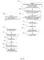
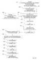
- FIG. 9is a flow diagram showing a process for assembly of a multi-package module as shown for example in FIG. 5A or FIG. 7.
- FIG. 10is a flow diagram showing a process for assembly of a multi-package module as shown for example in FIG. 6A.
- FIG. 11Ais a flow diagram showing a process for assembly of a multi-package module as shown for example in FIG. 8A.
- FIG. 11Bis a flow diagram showing a process for assembly of a multi-package module as shown for example in FIG. 8B.
- FIG. 11Cis a flow diagram showing a process for assembly of a multi-package module as shown for example in FIG. 8C.
- FIG. 5Athere is shown in a diagrammatic sectional view generally at 50 an embodiment of a multi-package module according to an aspect of the invention, including stacked first (“bottom”) and second (“top”) packages, in which the stacked packages are interconnected by wire bonding.
- the bottom package 400is a conventional BGA package such as that shown in FIG. 1.
- the bottom package 400includes a die 414 attached onto a bottom package substrate 412 having at least one metal layer.
- Any of various substrate typesmay be used, including for example: a laminate with 2-6 metal layers, or a build up substrate with 4-8 metal layers, or a flexible polyimide tape with 1-2 metal layers, or a ceramic multilayer substrate.
- the bottom package substrate 412 shown by way of example in FIG. 5Ahas two metal layers 421 , 423 , each patterned to provide appropriate circuitry and connected by way of vias 422 .
- the dieis conventionally attached to a surface of the substrate using an adhesive, typically referred to as the die attach epoxy, shown at 413 in FIG. 5A and, in the configuration in FIG. 5A, the surface of the substrate onto which the die is attached may be referred to as the “upper” surface, and the metal layer on that surface may be referred to as the “upper” metal layer, although the die attach surface need not have any particular orientation in use.
- the dieis wire bonded onto wire bond sites on the upper metal layer of the substrate to establish electrical connections.
- the die 414 and the wire bonds 416are encapsulated with a molding compound 417 that provides protection from ambient and from mechanical stress to facilitate handling operations, and provides a bottom package upper surface 419 onto which a second (“top”) package can be stacked.
- Solder balls 418are reflowed onto bonding pads on the lower metal layer of the substrate to provide interconnection to underlying circuitry of, for example, a motherboard (not shown in the FIGS.) of a final product, such as a computer.
- Solder masks 415 , 427are patterned over the metal layers 421 , 423 to expose the underlying metal at bonding sites for electrical connection, for example the wire bond sites and bonding pads for bonding the wire bonds 416 and solder balls 418 .
- the top package 500is a land grid array (“LGA”) package, which may be similar to a BGA package, as shown for example in FIG. 1, but having no solder balls mounted on bonding pads of the lower surface of the substrate.
- LGAland grid array
- the top package 500includes a die 514 attached onto a top package substrate 512 having at least one metal layer. Any of various substrate types may be used; the top package substrate 512 shown by way of example in FIG. 5A has two metal layers 521 , 523 , each patterned to provide appropriate circuitry and connected by way of vias 522 .
- the dieis conventionally attached to a surface of the substrate using an adhesive, typically referred to as the die attach epoxy, shown at 513 in FIG.
- the surface of the substrate onto which the die is attachedmay be referred to as the “upper” surface, and the metal layer on that surface may be referred to as the “upper” or “top” metal layer, although the die attach surface need not have any particular orientation in use.
- the dieis wire bonded onto wire bond sites on the upper metal layer of the substrate to establish electrical connections.
- the die 514 and the wire bonds 516are encapsulated with a molding compound 517 that provides protection from ambient and from mechanical stress to facilitate handling operations, and has a top package upper surface 519 .
- the top package 500is stacked over the bottom package 400 and affixed there using an adhesive 513 .
- Solder masks 515 , 527are patterned over the metal layers 521 , 523 to expose the underlying metal at bonding sites for electrical connection, for example the wire bond sites for bonding the wire bonds 516 .
- the z-interconnect between the stacked top package 500 and bottom package 400is made by way of wire bonds 518 connecting the top metal layers of the respective package substrates. At one end each wire bond 518 is electrically connected to upper surfaces of pads on the upper metal layer 521 of the top package substrate 512 , and at the other end each wire bond is connected to the upper surfaces of pads on the upper metal layer 421 of the bottom package substrate 412 .
- the wire bondsmay be formed by any wire bonding technique, well known in the art, such as is described, for example, in U.S. Pat. No. 5,226,582, which is hereby incorporated by reference herein.
- the package-to-package z-interconnect wire bondsare shown by way of example in FIG.
- the wire bondscan be made in the inverse direction, that is, by forming a bead or bump on the upper surface of a pad on the upper metal layer of the bottom substrate, and then drawing the wire upward toward and fusing it onto, a pad on the upper metal layer of the top substrate.
- selection of a wire bonding strategy for the package-to-package z-interconnectionwill be determined according to the geometric arrangements of the margins of the stacked substrates and of the bonding surfaces on them.
- the z-interconnect pads on the respective package substratesare arranged on the upper metal layers near the margins of the package substrates.
- the location and order of the z-interconnect padsare generally arranged so that the z-interconnect pads on the top package substrate approximately overlie the corresponding z-interconnect pads on the bottom package when the packages are stacked.
- the top package 500has a smaller substrate footprint than that of the bottom package 400 , to allow clearance for the wire bonds without electrical shorting to the edges of the metal layers of the substrates.
- top package z-interconnect pads 524are formed by patterning regions of the upper metal layer situated at the margin 501 on the upper surface 525 of the top package substrate 512 .
- the margin 501extends beyond the edge 526 of the top package encapsulant material, which has an upper surface 519 .
- bottom package z-interconnect pads 424are formed by patterning regions of the upper metal layer situated at the margin 401 on the upper surface 425 of the top package substrate 412 .
- the margin 401extends beyond the footprint 511 of the stacked and overlying top package substrate 512 , and further beyond the edge 426 of the bottom package encapsulant material, which has an upper surface 419 .
- z-interconnection between the top and bottom packages according to the inventionis made by wire bond between (either bond-up or bond-down) the top package interconnect pads 524 in the margin 501 of the top package substrate and the bottom package interconnect pads 424 in the margin 401 of the bottom package substrate.
- the multipackage module structureis protected by formation of a module encapsulant 507 , and solder balls 418 are reflowed onto exposed solder ball pads on the lower metal layer of the bottom package substrate, for connection to underlying circuitry, such as a motherboard (not shown in the FIGS.).
- the structure according to the inventionallows for pre-testing of both the BGA and LGA before assembly into the multi-package module, to permit rejection of nonconforming packages prior to assembly, and thereby to assure high final module test yields.
- a heat spreadermay be provided over the top package.
- the top heat spreaderis formed of a thermally conductive material having at least the more central area of its upper surface exposed at the upper surface of the MPM to ambient for efficient heat exchange away from the MPM.
- the top heat spreadermay be, for example, a sheet of metal (such as copper), and it may be affixed to the MPM encapsulant during the molding material curing process.
- the heatspreadermay have a generally planar portion over the top package, and a peripheral supporting portion or supporting members resting on or near the upper surface of the bottom package substrate.
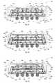
- FIG. 5Eis a diagrammatic sketch in a sectional view showing a stacked BGA+LGA MPM 54 according to another aspect of the invention, in which a “top” heat spreader is provided at the upper surface of the MPM.
- the construction of the stacked packages in MPM 54is generally similar to that of MPM 50 in FIG. 5A, and like structures are identified in the FIGS. by like reference numerals.
- the top heat spreader in this exampleis formed of a thermally conductive material having a generally planar central portion 544 situated over the top package, and peripheral supporting members 546 extending to the upper surface of the bottom package substrate 412 .
- the upper surface of the planar portion 544is exposed to ambient at the MPM upper surface for efficient heat exchange away from the MPM.
- the top heat spreadermay be formed, for example, of a sheet of metal (such as copper), for example by stamping.
- the supporting members 546can optionally be affixed to the upper surface of the bottom package substrate using an adhesive (not show in the FIGS.).
- the multi-package module structureis protected by formation of a module encapsulant 507 , and the heat spreader supporting members are embedded in the MPM encapsulant 507 during the molding material curing process. In the embodiment of FIG.
- a step like re-entrant feature 545is provided on the periphery of the planar upper portion 544 of the heat spreader to allow for better mechanical integrity of the structure with less delamination from the molding compound.
- the space between the lower surface of the heat spreader 544 and the upper surface 519 of the LGA molding 917is filled by a thin layer of the MPM molding.
- a top heat spreadercan be affixed to the upper surface of the LGA molding as shown diagrammatically in a sectional view in FIG. 5D.
- the construction of the stacked packages in MPM 52is generally similar to that of MPM 50 in FIG. 5A, and like structures are identified in the FIGS. by like reference numerals.
- the top heat spreader 504 in the example of FIG. 5Dis a generally planar piece of a thermally conductive material having at least the more central area of its upper surface exposed to ambient for efficient heat exchange away from the MPM, as in the example of FIG. 5E.
- the top heat spreadermay be, for example, a sheet of metal (such as copper).
- the top heat spreader 504is affixed onto the upper surface 519 of the upper package encapsulant 517 using an adhesive 506 .
- the adhesive 506may be a thermally conductive adhesive, to provide improved heat dissipation.
- the top heat spreaderis affixed to the top package molding after the top package molding has been at least partly cured, but before the molding material is injected for the MPM encapsulation 507 .
- the periphery of the top heat spreadermay be encapsulated with the MPM molding material.
- a step like re-entrant feature 505is provided on the periphery of the heat spreader 504 to allow for better mechanical integrity of the structure with less delamination from the molding compound.
- an MPM as in FIG. 5Acan be provided with a simple planar heat spreader, with no supporting members, that is not attached to the upper surface of the top package molding.
- the top heat spreadercan be a generally planar piece of a thermally conductive material such as, for example, a sheet of metal (such as copper), and at least the more central area of the upper surface of the planar heat spreader is exposed to ambient for efficient heat exchange away from the MPM.
- the space between the lower surface of the simple planar heat spreader and the upper surface 519 of the LGA molding 517may be filled by a thin layer of the MPM molding, and such a simple planar heat spreader may be affixed to the MPM encapsulant 507 during the molding material curing process.
- the periphery of such an unattached simple planar top heat spreadercan be encapsulated with the MPM molding material, as in the attached planar heat spreader of FIG. 5D, and may be provided with a step-like re-entrant feature 505 on the periphery to allow for better mechanical integrity of the structure with less delamination from the molding compound.
- An MPM structure having a heat spreader, as in FIGS. 5D, 5E,can provide improved thermal performance.
- FIG. 6Athere is shown a diagrammatic sketch in a sectional view showing a stacked package multi-package module according to an aspect of the invention, having an LGA top package stacked over a BGA bottom package, in which the top package LGA is partially encapsulated. That is, the molding material for the top LGA package is applied in limited regions and in limited amounts, sufficient to protect the wire bonds during subsequent handling, particularly during subsequent performance testing.
- the configuration of FIG. 6Ais substantially as shown in FIG. 5A. Accordingly, in this embodiment the bottom package 400 is constructed as described with reference to FIG. 5A, and the top package 600 is constructed substantially as described with reference to FIG. 5A, except for the difference in the top package encapsulation.
- the top package 600includes a die 614 attached onto a top package substrate 612 having at least one metal layer.
- a top package substrate 612having at least one metal layer.
- the top package substrate 512 shown by way of example in FIG. 6Ahas two metal layers 621 , 623 , each patterned to provide appropriate circuitry and connected by way of vias 622 .
- the dieis conventionally attached to a surface of the substrate using an adhesive, typically referred to as the die attach epoxy, shown at 613 in FIG. 6A and, in the configuration in FIG.
- the surface of the substrate onto which the die is attachedmay be referred to as the “upper” surface, and the metal layer on that surface may be referred to as the “upper” or “top” metal layer, although the die attach surface need not have any particular orientation in use.
- the dieis wire bonded onto wire bond sites on the upper metal layer of the substrate to establish electrical connections.
- the die 614 and the wire bonds 616are encapsulated with a molding compound 617 that provides protection from ambient and from mechanical stress to facilitate handling operations.
- the encapsulant 617 in this embodimentis formed such as to envelop the wire bonds and their respective connections to the top package substrate and the top package die only, so that much of the upper surface of the die 614 is not covered by the encapsulant.
- the top package 600is stacked over the bottom package 400 and affixed there using an adhesive. Solder masks 615 , 627 are patterned over the metal layers 621 , 623 to expose the underlying metal at bonding sites for electrical connection, for example the wire bond sites for bonding the wire bonds 616 .
- the z-interconnect between the stacked top package 600 and bottom package 400is made by way of wire bonds 618 connecting the top metal layers of the respective package substrates.
- the multipackage module structureis protected by formation of a module encapsulant 607 , and solder balls 418 are reflowed onto exposed solder ball pads on the lower metal layer of the bottom package substrate, for connection to underlying circuitry, such as a motherboard (not shown in the FIGS.).
- An advantage of this configurationis reduced cost.
- the partial encapsulationis implemented in line with the wire bonding process (for example by dispensation through a fine nozzle, as from a syringe through a hollow needle) and therefore provides a higher throughput and uses less encapsulant material. Subsequent to the partial encapsulation the top LGA package can be tested without resort to special handling to avoid damaging the top package wire bonds.
- a heat spreadermay be provided over the top package.
- the top heat spreaderis formed of a thermally conductive material having at least the more central area of its upper surface exposed at the upper surface of the MPM to ambient for efficient heat exchange away from the MPM.
- the top heat spreadermay be, for example, a sheet of metal (such as copper), and it may be affixed to the MPM encapsulant during the molding material curing process.
- the heatspreadermay have a generally planar portion over the top package, and a peripheral supporting portion or supporting members resting on or near the upper surface of the bottom package substrate.
- FIG. 6Bis a diagrammatic sketch in a sectional view showing a stacked BGA+LGA MPM 62 according to another aspect of the invention, in which a “top” heat spreader is provided at the upper surface of the MPM.
- the construction of the stacked packages in MPM 62is generally similar to that of MPM 60 in FIG. 6A, and like structures are identified in the FIGS. by like reference numerals.
- the top heat spreader in this exampleis formed of a thermally conductive material having a generally planar central portion 644 situated over the top package, and peripheral supporting members 646 extending to the upper surface of the bottom package substrate 412 .
- the upper surface of the planar portion 644is exposed to ambient at the MPM upper surface for efficient heat exchange away from the MPM.
- the top heat spreadermay be formed, for example, of a sheet of metal (such as copper), for example by stamping.
- the supporting members 646can optionally be affixed to the upper surface of the bottom package substrate using an adhesive (not shown in the FIGS.).
- the multi-package module structureis protected by formation of a module encapsulant 607 , and the heat spreader supporting members are embedded in the MPM encapsulant 607 during the molding material curing process. In the embodiment of FIG.
- a step like re-entrant feature 645is provided on the periphery of the planar upper portion 644 of the heat spreader to allow for better mechanical integrity of the structure with less delamination from the molding compound.
- the space between the lower surface of the heat spreader 644 and the upper surface of the die 614is filled by a layer of the MPM molding that is thick enough so that the heatspreader 644 doe not interfere with the peripheral LGA molding 617 .
- a MPM as in the embodiment of FIG. 6Acan be provided with a simple planar heat spreader, with no supporting members, that is not attached to the upper surface of the top package molding.
- the top heat spreadercan be a generally planar piece of a thermally conductive material such as, for example, a sheet of metal (such as copper), and at least the more central area of the upper surface of the planar heat spreader is exposed to ambient for efficient heat exchange away from the MPM.
- a thermally conductive materialsuch as, for example, a sheet of metal (such as copper)
- the space between the lower surface of the planar heat spreader and the upper surface of the die 614is filled by a layer of the MPM molding that is thick enough so that the heatspreader does not interfere with the peripheral LGA molding 617 .
- a simple planar heat spreadermay be affixed to the MPM encapsulant 607 during the molding material curing process.
- the periphery of such an unattached simple planar top heat spreadercan be encapsulated with the MPM molding material, as in the attached planar heat spreader of FIG. 5D, and may be provided with a step-like re-entrant feature on the periphery to allow for better mechanical integrity of the structure with less delamination from the molding compound.
- a spacermay be provided between the lower surface of the simple planar top heat spreader and the upper surface of the die 614 .
- the spacermay be affixed to the die and to the heat spreader using an adhesive; or, the spacer may be formed as an integral part, a spacer portion, of the heat spreader, and in, such embodiments the lower surface of the spacer portion of the heat spreader may be affixed to the upper surface of the die using an adhesive.
- the spacerpreferably is of a thermally conductive material, and the adhesive may be a thermally conductive adhesive, to provide improved heat dissipation.
- the top heat spreadermay be affixed to the top package after the top package molding has been at least partly cured, but before the molding material is injected for the MPM encapsulation 607 .
- the periphery of the top heat spreadermay be encapsulated with the MPM molding material.
- a step like re-entrant featuremay be provided on the periphery of the simple planar heat spreader to allow for better mechanical integrity of the structure with less delamination from the molding compound.
- An MPM structure having a heat spreaderas for example in FIG. 6B, can provide improved thermal performance.
- FIG. 7is a diagrammatic sketch in a sectional view showing a stacked multipackage module according to another aspect of the invention, having a top LGA package stacked over a BGA bottom package, in which a one metal layer substrate is employed for the top LGA package.
- the configuration of FIG. 7is substantially as shown in FIG. 5A.
- the bottom package 400is constructed as described with reference to FIG. 5A
- the top package 700is constructed substantially as described with reference to FIG. 5A, except for the difference in the structure of the top package substrate.
- the top package 700includes a die 714 attached onto a top package substrate 712 having one metal layer 721 , patterned to provide appropriate circuitry.
- the dieis conventionally attached to a surface of the substrate using an adhesive, typically referred to as the die attach epoxy, shown at 713 in FIG. 7 and, in the configuration in FIG. 7, the surface of the substrate onto which the die is attached may be referred to as the “upper” surface, and accordingly the metal layer on this substrate may be referred to as an “upper” or “top” metal layer, although the die attach surface need not have any particular orientation in use.
- an adhesivetypically referred to as the die attach epoxy
- the dieis wire bonded onto wire bond sites on the upper metal layer of the substrate to establish electrical connections.
- the die 714 and the wire bonds 716are encapsulated with a molding compound 717 that provides protection from ambient and from mechanical stress to facilitate handling operations.
- the encapsulant 717 in the embodiment as shown in FIG. 7is configured as in the FIG. 5A embodiment, so that the encapsulant 717 covers the die as well as the wire bonds and their connections, and the encapsulant has a surface 719 over the entire die and interconnects.
- the encapsulanthere can alternatively be formed as in the embodiment of FIG.
- top package 700is stacked over the bottom package 400 and affixed there using an adhesive, indicated at 703 .
- Solder masks 715are patterned over the metal layer 721 to expose the underlying metal at bonding sites for electrical connection, for example the wire bond sites for bonding the wire bonds 716 .
- the z-interconnect between the stacked top package 700 and bottom package 400is made by way of wire bonds 718 connecting the top metal layers of the respective package substrates.
- the multipackage module structureis protected by formation of a module encapsulant 707 , and solder balls 418 are reflowed onto exposed solder ball pads on the lower metal layer of the bottom package substrate, for connection to underlying circuitry, such as a motherboard (not shown in the FIGS.).
- An advantage of this configurationis reduced cost as compared with a configuration employing a two metal layer substrate in the top LGA package, because of the lower cost of the one metal layer substrate.
- This configurationadditionally provides a lower package profile because the one metal layer substrate is thinner than a substrate having two or more metal layers.
- FIG. 8Ais a diagrammatic sketch in a sectional view showing a stacked BGA+LGA MPM 80 according to another aspect of the invention, in which a heat spreader and electrical shield is provided to the bottom package.
- the embodiment shown by way of example in FIG. 8Ahas a top land grid array (“LGA”) package 800 stacked over a bottom ball grid array “BGA” package 402 , in which the top LGA package is constructed generally as is the top LGA package in FIG. 5A.
- LGAtop land grid array
- BGAball grid array
- the top LGA package 800may be similar to a BGA package, as shown for example in FIG. 1, but having no solder balls mounted on bonding pads of the lower surface of the substrate.
- the top package 800includes a die 814 attached onto a top package substrate 812 having at least one metal layer. Any of various substrate types may be used; the top package substrate 812 shown by way of example in FIG. 8A has two metal layers 821 , 823 , each patterned to provide appropriate circuitry and connected by way of vias 822 .
- the dieis conventionally attached to a surface of the substrate using an adhesive, typically referred to as the die attach epoxy, shown at 813 in FIG. 8A and, in the configuration in FIG.
- the surface of the substrate onto which the die is attachedmay be referred to as the “upper” surface, and the metal layer on that surface may be referred to as the “upper” or “top” metal layer, although the die attach surface need not have any particular orientation in use.
- the dieis wire bonded onto wire bond sites on the upper metal layer of the substrate to establish electrical connections.
- the die 814 and the wire bonds 816are encapsulated with a molding compound 817 that provides protection from ambient and from mechanical stress to facilitate handling operations, and has a top package upper surface 819 .
- Solder masks 815 , 827are patterned over the metal layers 821 , 823 to expose the underlying metal at bonding sites for electrical connection, for example the wire bond sites for bonding the wire bonds 816 .
- the bottom BGA package 402 in the embodiment of FIG. 8Ais a conventional BGA package such as that shown in FIG. 1, except that the bottom BGA package of FIG. 8A is not encapsulated with a molding compound; rather, it is provided with a heat spreader that can additionally act as an electrical shield, as described below. Accordingly, in this embodiment the bottom package 402 includes a die 414 attached onto a bottom package substrate 412 having at least one metal layer. Any of various substrate types may be used, including for example: a laminate with 2-6 metal layers, or a build up substrate with 4-8 metal layers, or a flexible polyimide tape with 1-2 metal layers, or a ceramic multilayer substrate.
- the die 8Ahas two metal layers 421 , 423 , each patterned to provide appropriate circuitry and connected by way of vias 422 .
- the dieis conventionally attached to a surface of the substrate using an adhesive, typically referred to as the die attach epoxy, shown at 413 in FIG. 8A and, in the configuration in FIG. 8A, the surface of the substrate onto which the die is attached may be referred to as the “upper” surface, and the metal layer on that surface may be referred to as the “upper” metal layer, although the die attach surface need not have any particular orientation in use.
- solder balls 418are reflowed onto bonding pads on the lower metal layer of the substrate to provide interconnection to underlying circuitry of, for example, a motherboard (not shown in the FIGS.) of a final product, such as a computer.
- Solder masks 415 , 427are patterned over the metal layers 421 , 423 to expose the underlying metal at bonding sites for electrical connection, for example the wire bond sites and bonding pads for bonding the wire bonds 416 and solder balls 418 .
- the bottom BGA package 402 of multipackage module 80is provided with a metallic (for example, copper) heat spreader that acts additionally as an electrical shield to electrically contain any electromagnetic radiation from the die in the lower BGA and thereby prevent interference with the die in the upper package.
- a “top” planar part of the heat spreader 406is supported above the substrate 412 and over the die 414 by legs or sidewalls 407 .
- Spots or lines 408 of an adhesiveserve to affix the heat spreader support 407 to the upper surface of the bottom substrate.
- the adhesivecan be a conductive adhesive, and can be electrically connected to the top metal layer 421 of the substrate 412 , particularly to a ground plane of the circuit and thereby establishing the heat spreader as an electrical shield.
- the adhesivecan be non-conductive and in such a configuration the heat spreader acts only as a heat spreading device.
- the supporting parts and the top part of the heat spreader 406enclose the die 414 and the wire bonds 416 , and can serve to protect those structures from ambient and from mechanical stress to facilitate handling operations and, particularly, during subsequent testing before the MPM assembly.
- the top package 800 of multipackage module 80is stacked over the bottom package 402 upon the planar surface of the heat spreader/shield 406 and affixed there using an adhesive 803 .
- the adhesive 803can be thermally conductive, to improve thermal dissipation; and the adhesive 803 can be electrically conductive, to establish electrical connection of the heat spreader 406 to a lower metal layer of the LGA package substrate, or it can be electrically insulating, thereby preventing electrical connection.
- the z-interconnection between the top package 800 and the bottom package 402 according to the inventionis made by wire bonds 818 between top package interconnect pads in the margin of the top package substrate 812 and bottom package interconnect pads in the margin of the bottom package substrate 402 .
- the wire bondsmay be formed in either up-bond or down-bond fashion.
- the multipackage module structureis protected by formation of a module encapsulant 807 . Openings may be provided in the supporting parts 407 of the heat spreader to allow the MPM molding material to fill in the enclosed space during encapsulation.
- Solder balls 418are reflowed onto exposed solder ball pads on the lower metal layer of the bottom package substrate 412 , for connection to underlying circuitry, such as a motherboard (not shown in the FIGS.).
- the structure according to the inventionallows for pre-testing of both the BGA and LGA before assembly into the multi-package module, to permit rejection of nonconforming packages prior to assembly, and thereby to assure high final module test yields.
- a heat spreadermay be provided over the top package.
- the top heat spreaderis formed of a thermally conductive material having at least the more central area of its upper surface exposed at the upper surface of the MPM to ambient for efficient heat exchange away from the MPM.
- the top heat spreadermay be, for example, a sheet of metal (such as copper), and it may be affixed to the MPM encapsulant during the molding material curing process.
- the heatspreadermay have a generally planar portion over the top package, and a peripheral supporting portion or supporting members resting on or near the upper surface of the bottom package substrate.
- FIG. 8Bis a diagrammatic sketch in a sectional view showing a stacked BGA+LGA MPM 82 according to another aspect of the invention, in which a “top” heat spreader is provided at the upper surface of the MPM.
- the construction of the stacked packages in MPM 82is generally similar to that of MPM 80 in FIG. 8A, and like structures are identified in the FIGS. by like reference numerals.
- the top heat spreader in this exampleis formed of a thermally conductive material having a generally planar central portion 804 situated over the top package, and peripheral supporting members 806 extending to the upper surface of the bottom package substrate 412 , the upper surface of the planar portion 804 is exposed to ambient at the MPM upper surface for efficient heat exchange away from the MPM.
- the top heat spreadermay be formed, for example, of a sheet of metal (such as copper), for example by stamping.
- the supporting members 806can optionally be affixed to the upper surface of the bottom package substrate using an adhesive (not show in the FIGS.).
- the multi-package module structureis protected by formation of a module encapsulant 807 , and the heat spreader supporting members are embedded in the MPM encapsulant 807 during the molding material curing process.
- a step like re-entrant feature 805is provided on the periphery of the planar upper portion 804 of the heat spreader to allow for better mechanical integrity of the structure with less delamination from the molding compound.
- the space between the lower surface of the heat spreader 804 and the upper surface 819 of the LGA molding 817is filled by a thin layer of the MPM molding.
- the top heat spreadercan be a generally planar piece of a thermally conductive material such as, for example, a sheet of metal (such as copper), with no supporting members. At least the more central area of the upper surface of the planar heat spreader is exposed to ambient for efficient heat exchange away from the MPM.
- a simple planar heat spreaderis shown in FIG. 8C at 844 , where the heat spreader is affixed to an upper surface of the top package molding. In FIG. 8B, however, the heat spreader is not attached to the upper surface of the top package molding.
- the space between the lower surface of the simple planar heat spreader and the upper surface 819 of the LGA molding 817is filled by a thin layer of the MPM molding, and such a simple planar heat spreader may be affixed to the MPM encapsulant 807 during the molding material curing process.
- the periphery of a simple planar top heat spreadercan in an embodiment such as in FIG. 8B be encapsulated with the MPM molding material, and may be provided with a step-like re-entrant feature on the periphery (refer to re-entrant feature 845 in the simple planar heat spreader 844 in FIG. 8C) to allow for better mechanical integrity of the structure with less delamination from the molding compound.
- a top heat spreadercan be affixed to the upper surface of the LGA molding as shown diagrammatically in a sectional view in FIG. 8C.
- the construction of the stacked packages in MPM 84is generally similar to that of MPM 80 in FIG. 8A, and like structures are identified in the FIGS. by like reference numerals.
- the top heat spreader 844 in the example of FIG. 8Cis a generally planar piece of a thermally conductive material having at least the more central area of its upper surface exposed to ambient for efficient heat exchange away from the MPM, as in the example of FIG. 8B.
- the top heat spreadermay be, for example, a sheet of metal (such as copper).
- the top heat spreader 804is affixed onto the upper surface 819 of the upper package encapsulant 817 using an adhesive 846 .
- the adhesive 846may be a thermally conductive adhesive, to provide improved heat dissipation.
- the top heat spreaderis affixed to the top package molding after the top package molding has been at least partly cured, but before the molding material is injected for the MPM encapsulation 847 .
- the periphery of the top heat spreadermay be encapsulated with the MPM molding material.
- a step like re-entrant feature 845is provided on the periphery of the heat spreader 844 to allow for better mechanical integrity of the structure with less delamination from the molding compound.
- An advantage of a structure as in FIGS. 8A, 8B, 8 Cis significant thermal performance and, optionally, electrical shielding at the bottom package, which can be particularly important critical, for example, in MPM that combine RF and digital chips. It is not necessary to have both a bottom package heat spreader and a top heat spreader for all applications. Alternately one or the other may be adequate depending on the end product needs.
- the inventionfeatures wire bonding as the z-interconnect method between stacked packages.
- all LGAs stacked on a lower BGAmust be smaller (in at least one dimension in the x-y plane) than the BGA to allow space at the periphery for the wire bonds.
- the wire diametertypically is of the order of 0.025 mm (0.050 to 0.010 mm range).
- the wire distance to the LGA substrate edgecan differ in various embodiments, but is no less than a wire diameter.
- the relative sizes of BGA and LGAare determined primarily by the maximum die size in each.
- the die thickness and mold cap thicknessprimarily determine how many die can be stacked in one package.
- testing of BGAsis well established in the industry, and typically is done by accessing contact to the solder ball pads.
- the LGAscan be tested in either of two ways, namely by accessing the LGA pads on the lower surface of the LGA of the substrate, similar to the pads of the solder balls in a BGA; or by accessing the z-interconnect pads on the upper surface of the substrate.
- the completed MPM assemblycan be tested in the same as for testing BGAs.
- the MPM assembly processis similar for the configurations according to the various aspects of the invention.
- the processincludes steps of providing a first molded package including a first package substrate and at least one die attached to the first package substrate, dispensing adhesive onto an upper surface of the first molded package, placing a second molded package including a second package substrate and at least one die such that a lower surface of the second substrate contacts the adhesive on the upper surface of the first package, during the adhesive, and forming z-interconnects between the first and second substrate.
- the packagescan be tested prior to assembly, and package is not meeting requirements for performance or reliability can be discarded, so that first packages and second package is tested as “good” are used in the assembled module.
- FIG. 9is a flow diagram showing a process for assembly of a multi-package module as shown for example in FIG. 5A or FIG. 7.
- a step 1202an unsingulated strip of ball grid array packages is provided.
- the die and wire bond structures on the ball grid array packagesare protected by a molding.
- the BGA packages in the strippreferably are tested (as indicated in the FIG. by *) for performance and reliability before they are taken to subsequent steps in the process. Only packages identified as “good” are subjected to subsequent treatment.
- adhesiveis dispensed over the upper surface of the molding on “good” BGA packages.
- singulated land grid array packagesare provided.
- the singulated LGA packagesare protected by a molding, and preferably are tested (*) and identified as “good”.
- a pick-and-place operationis carried out to place “good” LGA packages on the adhesive over the molding on the “good” BGA packages.
- the adhesiveis cured.
- a plasma clean operationis performed in preparation for a step 1214 in which wire bond z-interconnections are formed between the stacked top LGA and bottom BGA packages.
- an additional plasma cleanmay be performed, followed by the formation of the MPM molding in a step 1218 .
- the second-level interconnect solder ballsare attached to the underside of the module.
- the completed modulesare tested (*) and singulated from the strip, for example by saw singulation or by punch singulation, and packaged for further use.
- FIG. 10is a flow diagram showing a process for assembly of a multi-package module as shown for example in FIG. 6A.
- a step 1302an unsingulated strip of ball grid array packages is provided.
- the die and wire bond structures on the ball grid array packagesare protected by a molding.
- the BGA packages in the strippreferably are tested (as indicated in the FIG. by *) for performance and reliability before they are taken to subsequent steps in the process. Only packages identified as “good” are subjected to subsequent treatment.
- adhesiveis dispensed over the upper surface of the molding on “good” BGA packages.
- singulated land grid array packagesare provided.
- the singulated LGA packagesare protected by a peripheral molding, protecting the wire bonds, and preferably are tested (*) and identified as “good”.
- a pick-and-place operationis carried out to place “good” LGA packages on the adhesive over the molding on the “good” BGA packages.
- the adhesiveis cured.
- a plasma clean operationis performed in preparation for a step 1314 in which wire bond z-interconnections are formed between the stacked top LGA and bottom BGA packages.
- an additional plasma cleanmay be performed, followed by the formation of the MPM molding in a step 1318 .
- a step 1320the second-level interconnect solder balls are attached to the underside of the module.
- the completed modulesare tested (*) and singulated from the strip, for example by saw singulation or by punch singulation, and packaged for further use.
- FIG. 11Ais a flow diagram showing a process for assembly of a multi-package module as shown for example in FIG. 8A.
- a step 1402an unsingulated strip of ball grid array packages is provided.
- the BGA packageshave shields affixed over the die. The shields protect the die and wire bond structures on the ball grid array packages, and accordingly no package molding is required.
- the BGA packages in the strippreferably are tested (as indicated in the FIG. by *) for performance and reliability before they are taken to subsequent steps in the process. Only packages identified as “good” are subjected to subsequent treatment.
- adhesiveis dispensed over the upper surface of the shields on “good” BGA packages.
- a step 1406singulated land grid array packages are provided.
- the singulated LGA packagesare protected by a molding, and preferably are tested (*) and identified as “good”.
- a pick-and-place operationis carried out to place “good” LGA packages on the adhesive over the shields on the “good” BGA packages.
- the adhesiveis cured.
- a plasma clean operationis performed in preparation for a step 1414 in which wire bond z-interconnections are formed between the stacked top LGA and bottom BGA packages.
- an additional plasma cleanmay be performed, followed by the formation of the MPM molding in a step 1418 .
- a deflash operationmay be carried out, to decompose and remove undesirable organic material.
- the deflashmay be carried out by laser, or by chemical or plasma clean.
- the second-level interconnect solder ballsare attached to the underside of the module.
- the completed modulesare tested (*) and singulated from the strip, for example by saw singulation or by punch singulation, and packaged for further use.
- FIG. 11Bis a flow diagram showing a process for assembly of a multi-package module as shown for example in FIG. 8B. This process is similar to the one shown in FIG. 1A, with additional steps interposed for installation of the heat spreader by a “drop-in” mold operation. Like steps in the process are identified by like reference numerals in the FIGS.
- a step 1402an unsingulated strip of ball grid array packages is provided.
- the BGA packageshave shields affixed over the die. The shields protect the die and wire bond structures on the ball grid array packages, and accordingly no package molding is required.
- the BGA packages in the strippreferably are tested (as indicated in the FIG. by *) for performance and reliability before they are taken to subsequent steps in the process.
- a step 1404adhesive is dispensed over the upper surface of the shields on “good” BGA packages.
- step 1406singulated land grid array packages are provided. The singulated LGA packages are protected by a molding, and preferably are tested (*) and identified as “good”.
- step 1408a pick-and-place operation is carried out to place “good” LGA packages on the adhesive over the shields on the “good” BGA packages.
- step 1410the adhesive is cured.
- a plasma clean operationis performed in preparation for a step 1414 in which wire bond z-interconnections are formed between the stacked top LGA and bottom BGA packages.
- an additional plasma cleanmay be performed.
- a heat spreaderis dropped into each mold cavity in a cavity molding apparatus.
- a clean package stack from step 1416is dropped into the mold cavity over the heat spreader.
- an encapsulation materialis injected into the mold cavity, and cured to form the MPM molding.
- a deflash operationmay be carried out, to decompose and remove undesirable organic material.
- the deflashmay be carried out by laser, or by chemical or plasma clean.
- the second-level interconnect solder ballsare attached to the underside of the module.
- the completed modulesare tested (*) and singulated from the strip, for example by saw singulation or by punch singulation, and packaged for further use.
- FIG. 11Cis a flow diagram showing a process for assembly of a multi-package module as shown for example in FIG. 8C. This process is similar to the one shown in FIG. 11A, with additional steps interposed for installation of a planar heat spreader by attachment over the top package. Like steps in the process are identified by like reference numerals in the FIGS.
- a step 1402an unsingulated strip of ball grid array packages is provided.
- the BGA packageshave shields affixed over the die. The shields protect the die and wire bond structures on the ball grid array packages, and accordingly no package molding is required.
- the BGA packages in the strippreferably are tested (as indicated in the FIG. by *) for performance and reliability before they are taken to subsequent steps in the process.
- a step 1404adhesive is dispensed over the upper surface of the shields on “good” BGA packages.
- step 1406singulated land grid array packages are provided. The singulated LGA packages are protected by a molding, and preferably are tested (*) and identified as “good”.
- step 1408a pick-and-place operation is carried out to place “good” LGA packages on the adhesive over the shields on the “good” BGA packages.
- step 1410the adhesive is cured.
- a plasma clean operationis performed in preparation for a step 1414 in which wire bond z-interconnections are formed between the stacked top LGA and bottom BGA packages, and then an additional plasma clean may be performed.
- an adhesiveis dispensed over the upper surface of the top LGA package molding, and in a step 1433 , a pick-and-place operation is performed to place a planar heat spreader onto the adhesive of the top package molding.
- the adhesiveis cured.
- additional plasma cleanis carried out, and in a step 1418 , the MPM molding is formed.
- a deflash operationmay be carried out, to decompose and remove undesirable organic material.
- the deflashmay be carried out by laser, or by chemical or plasma clean.
- the second-level interconnect solder ballsare attached to the underside of the module.
- the completed modulesare tested (*) and singulated from the strip, for example by saw singulation or by punch singulation, and packaged for further use.
Landscapes
- Engineering & Computer Science (AREA)
- Microelectronics & Electronic Packaging (AREA)
- Power Engineering (AREA)
- Physics & Mathematics (AREA)
- Condensed Matter Physics & Semiconductors (AREA)
- General Physics & Mathematics (AREA)
- Computer Hardware Design (AREA)
- Health & Medical Sciences (AREA)
- Electromagnetism (AREA)
- Toxicology (AREA)
- Structures Or Materials For Encapsulating Or Coating Semiconductor Devices Or Solid State Devices (AREA)
Abstract
Description
- This application claims the benefit of U.S. Provisional Application No. 60/411,590, filed Sep. 17, 2002, which is hereby incorporated herein by reference.[0001]
- This application is related to U.S. application Ser. No. ______ (Atty Docket No. CPAC.1017-2), titled “Semiconductor multi-package module having wire bond interconnection between stacked packages”; U.S. application Ser. No. ______ (Atty Docket No. CPAC.1017-4), titled “Semiconductor multi-package module having wire bond interconnect between stacked packages and having electrical shield”; U.S. application Ser. No. ______ (Atty Docket No. CPAC.1017-5), titled “Semiconductor multi-package module having package stacked over die-up flip chip ball grid array package and having wire bond interconnect between stacked packages”; U.S. application Ser. No. ______ (Atty Docket No. CPAC.1017-6), titled “Semiconductor multi-package module having package stacked over die-down flip chip ball grid array package and having wire bond interconnect between stacked packages”; U.S. application Ser. No. ______ (Atty Docket No. CPAC.1017-7), titled “Semiconductor multi-package module including stacked-die packages and having wire bond interconnect between stacked packages”. This application and all the said related applications are being filed on the same date, and each of the said related applications is hereby incorporated herein by reference.[0002]
- This invention relates to semiconductor packaging.[0003]
- Portable electronic products such as mobile phones, mobile computing, and various consumer products require higher semiconductor functionality and performance in a limited footprint and minimal thickness and weight at the lowest cost. This has driven the industry to increase integration on the individual semiconductor chips.[0004]
- More recently the industry has begun implementing integration on the “z-axis,” that is, by stacking chips, and stacks of up to five chips in one package have been used. This provides a dense chip structure having the footprint of a one-chip package, in the range of 5×5 mm to 40×40 mm, and obtaining thicknesses that have been continuously decreasing from 2.3 mm to 0.5 mm. The cost of a stacked die package is only incrementally higher than the cost of a single die package and the assembly yields are high enough to assure a competitive final cost as compared to packaging the die in individual packages.[0005]
- The primary practical limitation to the number of chips that can be stacked in a stacked die package is the low final test yield of the stacked-die package. It is inevitable that some of the die in the package will be defective to some extent, and therefore the final package test yield will be the product of the individual die test yields, each of which is always less than 100%. This can be particularly a problem even if only two die are stacked in a package but one of them has low yield because of design complexity or technology.[0006]
- Another limitation is the low power dissipation of the package. The heat is transmitted from one die to the other and there is no significant dissipation path other than through the solder ball to the motherboard.[0007]
- A further limitation is electromagnetic interference between the stacked die, particularly between RF and digital die, because there is no electrical shielding of either die.[0008]
- Another approach to integrating on the “z-axis” is to stack die packages to form a multi-package module. Stacked packages can provide numerous advantages as compared to stacked-die packages.[0009]
- For instance, each package with its die can be electrically tested, and rejected unless it shows satisfactory performance, before the packages are stacked. As a result the final stacked multi-package module yields are maximized.[0010]
- More efficient cooling can be provided in stacked packages, by inserting a heat spreader between the packages in the stack as well as at the top of the module.[0011]
- Package stacking allows electromagnetic shielding of the RF die and avoids interference with other die in the module.[0012]
- Each die or more than one die can be packaged in a respective package in the stack using the most efficient first level interconnect technology for the chip type and configuration, such as wire bonding or flip chip, to maximize performance and minimize cost.[0013]
- The z-interconnect between packages in a stacked multi-package module is a critical technology from the standpoint of manufacturability, design flexibility and cost. Z-interconnects that have been proposed include peripheral solder ball connection, and flexible substrate folded over the top of the bottom package. The use of peripheral solder balls for z-interconnects in stacked multi-package modules limits the number of connections that can be made and limits design flexibility, and results in a thicker and higher cost package. Although the use of a flexible folding substrate provides in principle for design flexibility, there is no established manufacturing infrastructure for the folding process. Moreover, the use of a flexible folding substrate requires a two metal layer flex substrate, and these are expensive. Furthermore the folded flexible substrate approach is restricted to low pincount applications because of limits in routing the circuitry in two metal layer substrates.[0014]
- The various z-interconnect structures are described in further detail with reference to FIGS.[0015]1-4.
- FIG. 1 is a diagrammatic sketch in a sectional view illustrating the structure of a standard Ball Grid Array (“BGA”) package, well established in the industry, that can be used as a bottom package in a stacked multi-package module (“MPM”). The BGA, shown generally at[0016]10, includes a
die 14 attached onto asubstrate 12 having at least one metal layer. Any of various substrate types may be used, including for example: a laminate with 2-6 metal layers, or a build up substrate with 4-8 metal layers, or a flexible polyimide tape with 1-2 metal layers, or a ceramic multilayer substrate. Thesubstrate 12 shown by way of example in FIG. 1 has twometal layers vias 122. The die is conventionally attached to a surface of the substrate using an adhesive, typically referred to as the die attach epoxy, shown at13 in FIG. 1 and, in the configuration in FIG. 1, the surface of the substrate onto which the die is attached may be referred to as the “upper” surface, and the metal layer on that surface may be referred to as the “upper” metal layer, although the die attach surface need not have any particular orientation in use. - In the BGA of FIG. 1 the die is wire bonded onto wire bond sites on the upper metal layer of the substrate to establish electrical connections. The die[0017]14 and the
wire bonds 16 are encapsulated with a molding compound.17 that provides protection from ambient and from mechanical stress to facilitate handling operations, and provides a surface for marking for identification.Solder balls 18 are reflowed onto bonding pads on the lower metal layer of the substrate to provide interconnection to the motherboard (not shown in the FIGS.) of a final product, such as a computer.Solder masks metal layers wire bonds 16 andsolder balls 18. - FIG. 2 is a diagrammatic sketch in a sectional view illustrating the structure of an example of a 2-stack MPM, generally at[0018]20, in which the z-interconnect between the packages in the stack is made by way of solder balls. In this MPM a first package (which may be referred to as the “bottom” package) is similar to a standard BGA as shown in FIG. 1 (and similar reference numerals are employed to point to similar features of the bottom package in FIGS. 1 and 2). A second package (which may be referred to as the “top” package) is stacked on the bottom package and is similar in structure to the bottom package, except that the solder balls in the top package are arranged at the periphery of the top package substrate, so that they effect the z-interconnect without interference with the encapsulation of the bottom BGA. Particularly, the top package in FIG. 2 includes a die24 attached onto a
substrate 22 having at least one metal layer. Thetop package substrate 22 shown by way of example in FIG. 2 has twometal layers vias 222. The die is conventionally attached to a surface of the substrate (the “upper” surface) using an adhesive, typically referred to as the die attach epoxy, shown at23 in FIG. 2. - In the top package in the MPM of FIG. 2, as in the bottom package, the die is wire bonded onto wire bond sites on the upper metal layer of the substrate to establish electrical connections. The top package die[0019]24 and
wire bonds 26 are encapsulated with a toppackage molding compound 27.Solder balls 28 are reflowed onto bonding pads located on the peripheral margin of the lower metal layer of the top package substrate to provide z-interconnection to the bottom package. Solder masks225,227 are patterned over the metal layers221,223 to expose the underlying metal at bonding sites for electrical connection, for example the wire bond sites and bonding pads for bonding thewire bonds 26 andsolder balls 28. - The z-interconnection in the MPM of FIG. 2 is achieved by reflowing the[0020]
solder balls 28 attached to peripheral bonding pads on the lower metal layer of the top package substrate onto peripheral bonding pads on the upper metal layer of the bottom BGA. In this configuration the distance h between the top and bottom packages must be at least as great as the encapsulation height of the bottom package, which may be 0.3 mm or more, and typically is in a range between 0.5 mm and 1.5 mm. Thesolder balls 28 must accordingly be of a sufficiently large diameter that when they are reflowed they make good contact with the bonding pads of the bottom BGA; that is, thesolder ball 28 diameter must be greater than the encapsulation height. A larger ball diameter dictates a larger ball pitch that in turn limits the number of balls that can be fitted in the available space. Furthermore the peripheral arrangement of the solder balls forces the bottom BGA to be significantly larger than the mold cap of a standard BGA. In small BGAs, usually referred to as Chip Scale Packages (“CSP”), the package body size is 1.7 mm larger than the die. In standard BGAs the body size is about 2 mm larger than the mold cap. In this configuration the top package substrate must have at least 2 metal layers to facilitate the electrical connections. - FIG. 3 is a diagrammatic sketch in a sectional view illustrating the structure of an example of a known 2-stack flip chip MPM, shown generally at[0021]30. In this configuration the bottom BGA flip chip package includes a
substrate 32 having a patternedmetal layer 31 onto which thedie 34 is connected by flip chip bumps36, such as solder bumps, gold stud bumps or anisotropically conducting film or paste. The flip chip bumps are affixed to a patterned array of bump pads on the active surface of the die and, as the active surface of the die faces downward in relation to an upward-facing patterned metal layer of the substrate, such an arrangement may be referred to as a “die down”, flip chip package. Apolymer underfill 33 between die and substrate provides protection from ambient and adds mechanical integrity to the structure. Such a flip chip package, in which the substrate has a metal layer on only the upper surface, is connected to the underlying circuitry (such as a motherboard, not shown in the FIG.) bysolder balls 38 connected to the metal layer throughsolder vias 35. - The top BGA in this configuration is similar to the bottom BGA, except that the top BGA has z-[0022]
interconnect solder balls 338 connected (throughsolder vias 335 in the top substrate) to themetal layer 331 only at the periphery of the top substrate.Solder balls 338 are reflowed onto themetal layer 31 of the bottom substrate to provide the z-interconnect. Particularly, the top BGA in this configuration includes asubstrate 332 having a patternedmetal layer 331 onto which the top BGA die334 is connected by flip chip bumps336. Between the top BGA die and substrate is apolymer underfill 333. A structure as in FIG. 3 is more appropriate for high electrical performance applications, but it has similar limitations to configurations of the type shown in of FIG. 2. It presents an improvement over the FIG. 2 configuration in that the bottom BGA has no molding, allowing for use of smaller diameter (h) solder balls at the periphery of the top BGA for connection between the packages. - FIG. 4 is a diagrammatic sketch in a sectional view illustrating the structure of an example of a known 2-stack folded flexible substrate MPM, shown generally at[0023]40. The bottom package in the configuration of FIG. 4 has a 2-metal layer flexible substrate onto which the die is bonded via small beams to the first metal layer of the substrate. The second metal layer of the bottom package substrate carries the solder balls for connection to the underlying circuitry, such as a motherboard (not shown). The substrate is large enough to be folded over the top of the package, thus bringing the electrical interconnect lines upward where they are available for connection to the top package (an example of which is described below) by way of an array of solder balls on the top package. The space around the die and between the die and folded-over substrate is encapsulated to provide protection and rigidity.
- Referring to FIG. 4, the two-metal layer[0024]
bottom package substrate 42 includes afirst metal layer 141 and asecond metal layer 143, each patterned to provide appropriate circuitry and connected by way ofvias 142. A part of the first metal layer, over a part of the bottom substrate, is processed (for example, using an array of punches) to present an array of cantilever beams ortabs 46 arranged to correspond to an array of interconnect pads on the active surface of the bottom package die44. Over this part of thesubstrate 42, which may be referred to as the “die attach part”, thefirst metal layer 141 faces upwardly. The die is aligned, active surface downward, over the die attach part of the substrate, and the cantilevers and the corresponding interconnect pads are joined, typically for example by a “thermosonic” process employing a combination of pressure, heat, and ultrasonic energy to complete the electrical connections. Thedie 44 is affixed using an adhesive43, typically a die attach epoxy, onto the die attach part of theflexible substrate 42. Asecond metal layer 143 of thebottom package substrate 42 faces downwardly in the die attach part of the substrate.Solder balls 48 are reflowed onto bonding pads located on an array on the downward-facing part of thesecond metal layer 143 to provide for interconnection of the MPM to underlying circuitry (not shown). Asolder mask 147 is patterned over thesecond metal layer 143 to expose the underlying metal as bonding sites for electrical connection, including the bond pads for connection with the underlying circuitry by way ofsolder balls 48, and the bond pads for connection with the top package by way ofsolder balls 18, as described below. - Another part of the[0025]
bottom package substrate 42, extending adjacent the die-attach portion, is folded up and over the bottom package die44. On this folded-over portion of theflexible substrate 42 thefirst metal layer 143 faces upwardly. In the configuration of FIG. 4 the top package is generally similar to the BGA of FIG. 1, in which the die is wire bonded onto wire bond sites on the upper metal layer of the substrate to establish electrical connections. Particularly, the top package die14 is attached onto asubstrate 12 having (in this example) twometal layers vias 122. The die is conventionally attached to the upper surface of the top package substrate using an adhesive13, typically a die attach epoxy. Thedie 14 and thewire bonds 16 are encapsulated with amolding compound 17 that provides protection from ambient and from mechanical stress to facilitate handling operations, and provides a surface for marking for identification.Solder balls 18 are reflowed ontobonding pads 143 on the upward-facing metal layer of the folded-over bottom package substrate to provide z-interconnection between the top and the bottom packages. - An advantage of a structure as in FIG. 4 is that the folded-over substrate provides sufficient area on the upward-facing surface of the folded-over bottom package substrate to accommodate a full array of solder balls in the top package and to accommodate more complex interconnect between the two packages. It also provides for a small package footprint. A primary disadvantage of this configuration is the high cost of the substrate and the unavailability of folding technology and equipment.[0026]
- A common feature of all these stacked package configurations is that they enable pretesting of each package, and provide for production MPMs with higher final test yields.[0027]
- This invention is directed to multi-package modules having stacked packages. According to the invention, z-interconnection between the stacked packages in the MPM is wire bond based. Generally, the invention features various configurations of various stacked packages, and methods for stacking and interconnecting the various packages by wire-bonding based z-interconnection. In the multi-package module according to the invention the package stack can include any of a variety of BGA packages and/or any of a variety of Land Grid Array (“LGA”) packages; the package stack can include wire bonded and/or flip chip packages; the package stack can include a thermal enhancement feature enabled by one or more heat spreaders in or on the stack; the package stack can include one or more packages having a flip chip die bonded either to the top or to the bottom of the BGA or LGA; the package stack can include one or more BGA and/or LGA packages having more than one die in the package stacked or side by side; the stack can include electromagnetic shield for one or more of the packages; and the stack can include any substrate, laminate or build-up or flexible or ceramic, provided that the z-interconnect pads are made available for bonding on the periphery of the packages.[0028]
- In one general aspect the invention features a multi-package module having stacked lower and upper packages, each package including a die attached to a substrate, in which the upper and lower substrates are interconnected by wire bonding.[0029]
- The invention provides for excellent manufacturability, high design flexibility, and low cost to produce a stacked package module having a low profile and a small footprint. The wire bond z-interconnect is well established in the industry; it is the lowest cost interconnect technique and it is directly applicable, without significant modification, to the stacked multi-package modules of the invention. It provides design flexibility to the relative size of the BGA to LGA that can be bridged by wire length. Using available techniques and equipment the wire in a wire bond can be as short as 0.5 mm or as long as 5 mm. The arrangement of the z-interconnect pads can be implemented through either or both BGA and LGA substrate designs. Moreover, using wire bonds according to the invention z-interconnect can be formed between pads that are not precisely aligned over one another, by employing so-called “out of sequence bonding” that is in current use in the industry. The wire bonding pitch is the finest available technology in the industry at 50 microns currently, and projected to go to 25 microns. This enables a high number of z-interconnects. Both manufacturability and design flexibility contribute to the low cost of the MPM.[0030]
- A minimum footprint for a typical BGA or LGA is 1.7 mm larger than the die size. The addition of the z-interconnect bond pads according to the invention will increase the BGA size minimally, by 0.8 mm. A typical BGA thickness is 1.0 mm and LGA thickness is 0.8 mm. Atypical adhesive thickness can be in the range 0.025 mm to 0.100 mm. Both the footprint and the thickness of the stacked package MPM according to the invention fall within accepted ranges for most applications.[0031]
- In some embodiments the multi-package module includes three or more packages, affixed serially to form a stack.[0032]
- In another aspect the invention features a multi-package module having stacked first (“bottom”) and second (“top”) packages, each package including a die attached to a substrate and connected to the substrate by wire bonding, in which the top package substrate and the bottom package substrate are interconnected by wire bonding. In some embodiments each package is fully encapsulated with a molding material; in other embodiments at least one of the packages is encapsulated only to an extent sufficient to protect the wire bonds between the die and the substrate during subsequent handling and testing. In some embodiments the second package is an LGA package, and in some such embodiments the LGA package substrate is a single-metal layer substrate.[0033]
- In another aspect the invention features a multi-package module having stacked first (“bottom”) and second (“top”) packages, the bottom package being a BGA package, each package including a die attached to a substrate, in which the top package substrate and the BGA package substrate are interconnected by wire bonding.[0034]
- In another aspect the invention features a multi-package module having stacked packages in which at least one package is provided with an electrical shield. In some such configurations the electrical shield may additionally be configured to serve as a heat spreader. In some embodiments the package that is provided with an electrical shield includes an RF die, and the shield serves to limit electromagnetic interference between the RF die and other die in the multi-package module. In some embodiments the bottom package is provided with an electrical shield.[0035]
- In another general aspect the invention features methods for making multi-package modules, by providing a first (bottom) package including at least one die on a first (bottom) package substrate, placing over the first package a second (top) package including at least one die on a second (top) package substrate, and forming wire bond z-interconnects between the first and second (top and bottom) substrates. Advantageously, the packages can be tested prior to assembly, and packages not meeting requirements for performance or reliability can be discarded, so that preferably only first packages and second packages tested as “good” are used in the assembled module.[0036]
- In one aspect the invention features a method for making a multi-package module including a LGA package stacked over a BGA package, in which the top and bottom packages are electrically interconnected by wire bonding. According to this aspect, a BGA package is provided, usually in an unsingulated strip of molded BGA packages; preferably the BGA packages in the strip are tested for performance and reliability and packages identified as “good” are subjected to subsequent treatment; adhesive is dispensed over the upper surface of the molding on “good” BGA packages; a singulated molded land grid array package is provided; preferably the LGA package is tested and identified as “good”; the “good” LGA package is placed onto the adhesive over the molding on the “good” BGA package, and the adhesive is cured; optionally and preferably a plasma clean operation is performed followed by formation of wire bond z-interconnections between the stacked top LGA and bottom BGA package; optionally and preferably an additional plasma clean may be performed, followed by the formation of the MPM molding. Further steps include attachment of second-level interconnect solder balls to the underside of the module; testing and singulation of the completed module from the strip, for example by saw singulation or by punch singulation; and packaging for further use.[0037]
- In, some embodiments the LGA (top) package is fully molded, providing a generally planar upper surface of the LGA package; in other embodiments the wire bonds but not the entire upper die surface of the LGA package is molded, molding of the LGA being carried out by dispensing the molding compound only around the periphery of the die and the margin of the LGA package substrate[0038]
- In another aspect the invention features a method for making a multi-package module including a LGA package stacked over a BGA package, in which the top and bottom packages are electrically interconnected by wire bonding, and in which the bottom package is provided with an electromagnetic shield. According to this aspect, a ball grid array package is provided, usually in an unsingulated strip of BGA packages; the BGA packages are provided with shields affixed over the die; preferably the BGA packages in the strip are tested for performance and reliability and packages identified as “good” are subjected to subsequent treatment; adhesive is dispensed over the upper surface of the shields on “good” BGA packages; a singulated molded land grid array package is provided; preferably the LGA package is tested and identified as “good”; the “good” LGA package is placed onto the adhesive over the shield, and the adhesive is cured; optionally and preferably a plasma clean operation is performed followed by formation of wire bond z-interconnections between the stacked top LGA and bottom BGA package; optionally and preferably an additional plasma clean may be performed, followed by the formation of the MPM molding. Further steps include attachment of second-level interconnect solder balls to the underside of the module; testing and singulation of the completed module from the strip, for example by saw singulation or by punch singulation; and packaging for further use.[0039]
- In some embodiments the method includes steps for providing the multi-package module with a heat spreader. In this aspect of the invention a similar process is performed, with additional steps interposed installation of supported heat spreader by a “drop-in” mold operation, or for installation of a simple planar heat spreader by a drop-in mold operation; or by applying adhesive onto an upper surface of the top package molding or onto an upper surface of a spacer upon the top package, and affixing the planar heat spreader onto the adhesive.[0040]
- In some embodiments of the method two or more first molded packages are provided in an unsingulated strip, and assembly of the two or more modules proceeds on the strip, and singulation of the two or more modules is carried out after assembly has been completed.[0041]
- In methods according to the invention for making multi-package modules the electrical connections between the stacked packages employs conventional wire bonding to form the z-interconnect between upper and lower package substrates in the stack. Particular advantages include the use of established manufacturing infrastructure, low production cost, design flexibility, and a thin package product. The z-interconnect wire bonding can be carried out, in the various package and module configurations, by drawing the wire to a conductive pad on the first package substrate from a bump formed on a conductive pad on the second package substrate; or, by drawing the wire to a conductive pad on the second package substrate from a bump formed on a conductive pad on the first package substrate.[0042]
- The invention provides for assembly of more than one semiconductor in a thin and minimal footprint package at the lowest cost and highest final test yield. Furthermore some stack configurations according to the invention allow for high thermal performance, high electrical performance or electrical isolation of an RF component from a digital one. Other stack configurations provide a very thin structure appropriate for handheld or consumer products. All provide for a method for assembly that allows individual testing of the stacked packages to maximize the final yield of the module.[0043]
- Additional process steps will be employed to complete the multi-package module according to the invention. For example, it may be preferred not to attach solder balls for connection of the lowermost package in the stack to the motherboard until the final step before singulation of the MPMs. And, for example, a plasma clean may be performed at any of a variety of points in the process, such as following adhesive cure and prior to encapsulation, and such as prior to and/or following z-interconnect wire bonding.[0044]
- Advantageously, the individual packages can be provided as strips of several packages, connected in a row for ease of handling during manufacture, and the multi-package modules are singulated following completion of process steps. In methods according to the invention, the package stacks can be formed on a strip of nonsingulated first packages of a selected type by affixing singulated second packages and forming the wire bonded z-interconnects until the process of forming the modules is complete, and then singulating the modules.[0045]
- MPM according to the invention can be used for building computers, telecommunications equipment, and consumer and industrial electronics devices.[0046]
- FIG. 1 is a diagrammatic sketch in a sectional view thru a conventional ball grid array semiconductor package.[0047]
- FIG. 2 is a diagrammatic sketch in a sectional view thru a conventional multi-package module having solder ball z-interconnection between stacked ball grid array semiconductor packages.[0048]
- FIG. 3 is a diagrammatic sketch in a sectional view thru a conventional flip chip multi-package module having solder ball z-interconnection between stacked flip chip semiconductor packages.[0049]
- FIG. 4 is a diagrammatic sketch in a sectional view thru a conventional multi-package module having a folded flexible substrate and solder ball z-interconnection between stacked semiconductor packages.[0050]
- FIG. 5A is a diagrammatic sketch in a sectional view thru an embodiment of a multi-package module having wire bond z-interconnection between stacked BGA and LGA semiconductor packages according to an aspect of the invention.[0051]
- FIG. 5B is a diagrammatic sketch in a plan view showing a bottom BGA substrate having z-interconnect bond pads in an arrangement suitable for use in an embodiment of the invention as shown in FIG. 5A.[0052]
- FIG. 5C is a diagrammatic sketch in a plan view showing a top LGA substrate having z-interconnect bond pads in an arrangement suitable for use in an embodiment of the invention as shown in FIG. 5A.[0053]
- FIG. 5D is a diagrammatic sketch in a sectional view thru an embodiment of a multi-package module having wire bond z-interconnection between stacked BGA and LGA semiconductor packages according to an aspect of the invention, and having a heat spreader affixed to an upper surface of the top package.[0054]
- FIG. 5E is a diagrammatic sketch in a sectional view thru an embodiment of a multi-package module having wire bond z-interconnection between stacked BGA and LGA semiconductor packages, and having a heat spreader according to another aspect of the invention.[0055]
- FIG. 6A is a diagrammatic sketch in a sectional view thru another embodiment of a multi-package module having wire bond z-interconnection between stacked BGA and LGA semiconductor packages according to an aspect of the invention, in which the top package is provided with peripheral molding.[0056]
- FIG. 6B is a diagrammatic sketch in a sectional view thru another embodiment of a multi-package module having wire bond z-interconnection between stacked BGA and LGA semiconductor packages according to an aspect of the invention, in which the top package is provided with peripheral molding, and the module is provided with a heat spreader.[0057]
- FIG. 7 is a diagrammatic sketch in a sectional view thru another embodiment of a multi-package module having wire bond z-interconnection between stacked BGA and LGA semiconductor packages according to an aspect of the invention, in which the top package substrate has a one metal layer substrate.[0058]
- FIG. 8A is a diagrammatic sketch in a sectional view thru an embodiment of a multi-package module having wire bond z-interconnection between stacked BGA and LGA semiconductor packages according to a further aspect of the invention, in which an electrical shield is provided on the bottom package.[0059]
- FIG. 8B is a diagrammatic sketch in a sectional view thru another embodiment of a multi-package module having wire bond z-interconnection between stacked BGA and LGA semiconductor packages according to an aspect of the invention, in which an electrical shield is provided on the bottom package, and the module is provided with a heat spreader.[0060]
- FIG. 8C is a diagrammatic sketch in a sectional view thru another embodiment of a multi-package module having wire bond z-interconnection between stacked BGA and LGA semiconductor packages according to an aspect of the invention, in which an electrical shield is provided on the bottom package, and the module is provided with a heat spreader affixed to an upper surface of the top package.[0061]
- FIG. 9 is a flow diagram showing a process for assembly of a multi-package module as shown for example in FIG. 5A or FIG. 7.[0062]
- FIG. 10 is a flow diagram showing a process for assembly of a multi-package module as shown for example in FIG. 6A.[0063]
- FIG. 11A is a flow diagram showing a process for assembly of a multi-package module as shown for example in FIG. 8A.[0064]
- FIG. 11B is a flow diagram showing a process for assembly of a multi-package module as shown for example in FIG. 8B.[0065]
- FIG. 11C is a flow diagram showing a process for assembly of a multi-package module as shown for example in FIG. 8C.[0066]
- The invention will now be described in further detail by reference to the drawings, which illustrate alternative embodiments of the invention. The drawings are diagrammatic, showing features of the invention and their relation to other features and structures, and are not made to scale. For improved clarity of presentation, in the FIGS. illustrating embodiments of the invention, elements corresponding to elements shown in other drawings are not all particularly renumbered, although they are all readily identifiable in all the FIGS.[0067]
- Turning now to FIG. 5A, there is shown in a diagrammatic sectional view generally at[0068]50 an embodiment of a multi-package module according to an aspect of the invention, including stacked first (“bottom”) and second (“top”) packages, in which the stacked packages are interconnected by wire bonding. In the embodiment shown in FIG. 5A, the
bottom package 400 is a conventional BGA package such as that shown in FIG. 1. Accordingly, in this embodiment thebottom package 400 includes a die414 attached onto abottom package substrate 412 having at least one metal layer. Any of various substrate types may be used, including for example: a laminate with 2-6 metal layers, or a build up substrate with 4-8 metal layers, or a flexible polyimide tape with 1-2 metal layers, or a ceramic multilayer substrate. Thebottom package substrate 412 shown by way of example in FIG. 5A has twometal layers vias 422. The die is conventionally attached to a surface of the substrate using an adhesive, typically referred to as the die attach epoxy, shown at413 in FIG. 5A and, in the configuration in FIG. 5A, the surface of the substrate onto which the die is attached may be referred to as the “upper” surface, and the metal layer on that surface may be referred to as the “upper” metal layer, although the die attach surface need not have any particular orientation in use. - In the bottom BGA package of FIG. 5A the die is wire bonded onto wire bond sites on the upper metal layer of the substrate to establish electrical connections. The[0069]
die 414 and thewire bonds 416 are encapsulated with amolding compound 417 that provides protection from ambient and from mechanical stress to facilitate handling operations, and provides a bottom packageupper surface 419 onto which a second (“top”) package can be stacked.Solder balls 418 are reflowed onto bonding pads on the lower metal layer of the substrate to provide interconnection to underlying circuitry of, for example, a motherboard (not shown in the FIGS.) of a final product, such as a computer. Solder masks415,427 are patterned over the metal layers421,423 to expose the underlying metal at bonding sites for electrical connection, for example the wire bond sites and bonding pads for bonding thewire bonds 416 andsolder balls 418. - In the embodiment shown in FIG. 5A, the[0070]
top package 500 is a land grid array (“LGA”) package, which may be similar to a BGA package, as shown for example in FIG. 1, but having no solder balls mounted on bonding pads of the lower surface of the substrate. Particularly, in this example, thetop package 500 includes a die514 attached onto atop package substrate 512 having at least one metal layer. Any of various substrate types may be used; thetop package substrate 512 shown by way of example in FIG. 5A has twometal layers vias 522. The die is conventionally attached to a surface of the substrate using an adhesive, typically referred to as the die attach epoxy, shown at513 in FIG. 5A and, in the configuration in FIG. 5A, the surface of the substrate onto which the die is attached may be referred to as the “upper” surface, and the metal layer on that surface may be referred to as the “upper” or “top” metal layer, although the die attach surface need not have any particular orientation in use. - In the top LGA package in the embodiment of FIG. 5A the die is wire bonded onto wire bond sites on the upper metal layer of the substrate to establish electrical connections. The[0071]
die 514 and thewire bonds 516 are encapsulated with amolding compound 517 that provides protection from ambient and from mechanical stress to facilitate handling operations, and has a top packageupper surface 519. Thetop package 500 is stacked over thebottom package 400 and affixed there using an adhesive513. Solder masks515,527 are patterned over the metal layers521,523 to expose the underlying metal at bonding sites for electrical connection, for example the wire bond sites for bonding the wire bonds516. - The z-interconnect between the stacked[0072]
top package 500 andbottom package 400 is made by way ofwire bonds 518 connecting the top metal layers of the respective package substrates. At one end eachwire bond 518 is electrically connected to upper surfaces of pads on theupper metal layer 521 of thetop package substrate 512, and at the other end each wire bond is connected to the upper surfaces of pads on theupper metal layer 421 of thebottom package substrate 412. The wire bonds may be formed by any wire bonding technique, well known in the art, such as is described, for example, in U.S. Pat. No. 5,226,582, which is hereby incorporated by reference herein. The package-to-package z-interconnect wire bonds are shown by way of example in FIG. 5A as having been made by forming a bead or bump on the upper surface of a pad on the upper metal layer of the top substrate, and then drawing the wire downward toward and fusing it onto, a pad on the upper metal layer of the bottom substrate. As will be appreciated, the wire bonds can be made in the inverse direction, that is, by forming a bead or bump on the upper surface of a pad on the upper metal layer of the bottom substrate, and then drawing the wire upward toward and fusing it onto, a pad on the upper metal layer of the top substrate. As will be appreciated, selection of a wire bonding strategy for the package-to-package z-interconnection will be determined according to the geometric arrangements of the margins of the stacked substrates and of the bonding surfaces on them. - In the stacked package embodiment of FIG. 5A, the z-interconnect pads on the respective package substrates are arranged on the upper metal layers near the margins of the package substrates. The location and order of the z-interconnect pads are generally arranged so that the z-interconnect pads on the top package substrate approximately overlie the corresponding z-interconnect pads on the bottom package when the packages are stacked. Conveniently, the[0073]
top package 500 has a smaller substrate footprint than that of thebottom package 400, to allow clearance for the wire bonds without electrical shorting to the edges of the metal layers of the substrates. Once the z-interconnect wire bonds have been formed, a module encapsulation is formed, to enclose and protect the z-interconnect wire bonds and to provide mechanical integrity to the completed module. - The arrangements of the z-interconnect pads on the top and bottom package substrates are shown by way of example in diagrammatic plan view in FIGS. 5B and 5C, generally at[0074]500 and400, respectively. Referring to FIG. 5B, top package z-
interconnect pads 524 are formed by patterning regions of the upper metal layer situated at themargin 501 on theupper surface 525 of thetop package substrate 512. Themargin 501 extends beyond theedge 526 of the top package encapsulant material, which has anupper surface 519. Referring now to FIG. 5C, bottom package z-interconnect pads 424 are formed by patterning regions of the upper metal layer situated at themargin 401 on theupper surface 425 of thetop package substrate 412. Themargin 401 extends beyond thefootprint 511 of the stacked and overlyingtop package substrate 512, and further beyond theedge 426 of the bottom package encapsulant material, which has anupper surface 419. - As will be apparent from FIGS. 5A, 5B and[0075]5C, z-interconnection between the top and bottom packages according to the invention is made by wire bond between (either bond-up or bond-down) the top
package interconnect pads 524 in themargin 501 of the top package substrate and the bottompackage interconnect pads 424 in themargin 401 of the bottom package substrate. The multipackage module structure is protected by formation of amodule encapsulant 507, andsolder balls 418 are reflowed onto exposed solder ball pads on the lower metal layer of the bottom package substrate, for connection to underlying circuitry, such as a motherboard (not shown in the FIGS.). - As will be appreciated from the foregoing, the structure according to the invention allows for pre-testing of both the BGA and LGA before assembly into the multi-package module, to permit rejection of nonconforming packages prior to assembly, and thereby to assure high final module test yields.[0076]
- For improved heat dissipation from the multi-package module, a heat spreader may be provided over the top package. The top heat spreader is formed of a thermally conductive material having at least the more central area of its upper surface exposed at the upper surface of the MPM to ambient for efficient heat exchange away from the MPM. The top heat spreader may be, for example, a sheet of metal (such as copper), and it may be affixed to the MPM encapsulant during the molding material curing process. Or, the heatspreader may have a generally planar portion over the top package, and a peripheral supporting portion or supporting members resting on or near the upper surface of the bottom package substrate.[0077]
- By way of example, FIG. 5E is a diagrammatic sketch in a sectional view showing a stacked BGA+[0078]
LGA MPM 54 according to another aspect of the invention, in which a “top” heat spreader is provided at the upper surface of the MPM. The construction of the stacked packages inMPM 54 is generally similar to that ofMPM 50 in FIG. 5A, and like structures are identified in the FIGS. by like reference numerals. The top heat spreader in this example is formed of a thermally conductive material having a generally planarcentral portion 544 situated over the top package, and peripheral supportingmembers 546 extending to the upper surface of thebottom package substrate 412. The upper surface of theplanar portion 544 is exposed to ambient at the MPM upper surface for efficient heat exchange away from the MPM. The top heat spreader may be formed, for example, of a sheet of metal (such as copper), for example by stamping. The supportingmembers 546 can optionally be affixed to the upper surface of the bottom package substrate using an adhesive (not show in the FIGS.). The multi-package module structure is protected by formation of amodule encapsulant 507, and the heat spreader supporting members are embedded in the MPM encapsulant507 during the molding material curing process. In the embodiment of FIG. 5E a step likere-entrant feature 545 is provided on the periphery of the planarupper portion 544 of the heat spreader to allow for better mechanical integrity of the structure with less delamination from the molding compound. In this embodiment the space between the lower surface of theheat spreader 544 and theupper surface 519 of the LGA molding917 is filled by a thin layer of the MPM molding. - Alternatively, a top heat spreader can be affixed to the upper surface of the LGA molding as shown diagrammatically in a sectional view in FIG. 5D. The construction of the stacked packages in[0079]
MPM 52 is generally similar to that ofMPM 50 in FIG. 5A, and like structures are identified in the FIGS. by like reference numerals. Thetop heat spreader 504 in the example of FIG. 5D is a generally planar piece of a thermally conductive material having at least the more central area of its upper surface exposed to ambient for efficient heat exchange away from the MPM, as in the example of FIG. 5E. The top heat spreader may be, for example, a sheet of metal (such as copper). Here, however, thetop heat spreader 504 is affixed onto theupper surface 519 of theupper package encapsulant 517 using an adhesive506. The adhesive506 may be a thermally conductive adhesive, to provide improved heat dissipation. Usually the top heat spreader is affixed to the top package molding after the top package molding has been at least partly cured, but before the molding material is injected for theMPM encapsulation 507. The periphery of the top heat spreader may be encapsulated with the MPM molding material. In the embodiment of FIG. 5D a step likere-entrant feature 505 is provided on the periphery of theheat spreader 504 to allow for better mechanical integrity of the structure with less delamination from the molding compound. - As a further alternative, an MPM as in FIG. 5A can be provided with a simple planar heat spreader, with no supporting members, that is not attached to the upper surface of the top package molding. In such embodiments, as in the embodiment of FIG. 5D, the top heat spreader can be a generally planar piece of a thermally conductive material such as, for example, a sheet of metal (such as copper), and at least the more central area of the upper surface of the planar heat spreader is exposed to ambient for efficient heat exchange away from the MPM. Here, the space between the lower surface of the simple planar heat spreader and the[0080]
upper surface 519 of theLGA molding 517 may be filled by a thin layer of the MPM molding, and such a simple planar heat spreader may be affixed to the MPM encapsulant507 during the molding material curing process. The periphery of such an unattached simple planar top heat spreader can be encapsulated with the MPM molding material, as in the attached planar heat spreader of FIG. 5D, and may be provided with a step-likere-entrant feature 505 on the periphery to allow for better mechanical integrity of the structure with less delamination from the molding compound. - An MPM structure having a heat spreader, as in FIGS. 5D, 5E, can provide improved thermal performance.[0081]
- Referring now to FIG. 6A there is shown a diagrammatic sketch in a sectional view showing a stacked package multi-package module according to an aspect of the invention, having an LGA top package stacked over a BGA bottom package, in which the top package LGA is partially encapsulated. That is, the molding material for the top LGA package is applied in limited regions and in limited amounts, sufficient to protect the wire bonds during subsequent handling, particularly during subsequent performance testing. In other respects the configuration of FIG. 6A is substantially as shown in FIG. 5A. Accordingly, in this embodiment the[0082]
bottom package 400 is constructed as described with reference to FIG. 5A, and thetop package 600 is constructed substantially as described with reference to FIG. 5A, except for the difference in the top package encapsulation. Particularly, thetop package 600 includes a die614 attached onto atop package substrate 612 having at least one metal layer. Any of various substrate types may be used; thetop package substrate 512 shown by way of example in FIG. 6A has twometal layers vias 622. The die is conventionally attached to a surface of the substrate using an adhesive, typically referred to as the die attach epoxy, shown at613 in FIG. 6A and, in the configuration in FIG. 6A, the surface of the substrate onto which the die is attached may be referred to as the “upper” surface, and the metal layer on that surface may be referred to as the “upper” or “top” metal layer, although the die attach surface need not have any particular orientation in use. - In the top LGA package in the embodiment of FIG. 6A the die is wire bonded onto wire bond sites on the upper metal layer of the substrate to establish electrical connections. The[0083]
die 614 and thewire bonds 616 are encapsulated with amolding compound 617 that provides protection from ambient and from mechanical stress to facilitate handling operations. Theencapsulant 617 in this embodiment is formed such as to envelop the wire bonds and their respective connections to the top package substrate and the top package die only, so that much of the upper surface of thedie 614 is not covered by the encapsulant. Thetop package 600 is stacked over thebottom package 400 and affixed there using an adhesive. Solder masks615,627 are patterned over the metal layers621,623 to expose the underlying metal at bonding sites for electrical connection, for example the wire bond sites for bonding the wire bonds616. - The z-interconnect between the stacked[0084]
top package 600 andbottom package 400 is made by way ofwire bonds 618 connecting the top metal layers of the respective package substrates. The multipackage module structure is protected by formation of amodule encapsulant 607, andsolder balls 418 are reflowed onto exposed solder ball pads on the lower metal layer of the bottom package substrate, for connection to underlying circuitry, such as a motherboard (not shown in the FIGS.). - An advantage of this configuration is reduced cost. The partial encapsulation is implemented in line with the wire bonding process (for example by dispensation through a fine nozzle, as from a syringe through a hollow needle) and therefore provides a higher throughput and uses less encapsulant material. Subsequent to the partial encapsulation the top LGA package can be tested without resort to special handling to avoid damaging the top package wire bonds.[0085]
- For improved heat dissipation from the multi-package module as shown for example in FIG. 6A, a heat spreader may be provided over the top package. The top heat spreader is formed of a thermally conductive material having at least the more central area of its upper surface exposed at the upper surface of the MPM to ambient for efficient heat exchange away from the MPM. The top heat spreader may be, for example, a sheet of metal (such as copper), and it may be affixed to the MPM encapsulant during the molding material curing process. Or, the heatspreader may have a generally planar portion over the top package, and a peripheral supporting portion or supporting members resting on or near the upper surface of the bottom package substrate.[0086]
- By way of example, FIG. 6B is a diagrammatic sketch in a sectional view showing a stacked BGA+[0087]
LGA MPM 62 according to another aspect of the invention, in which a “top” heat spreader is provided at the upper surface of the MPM. The construction of the stacked packages inMPM 62 is generally similar to that ofMPM 60 in FIG. 6A, and like structures are identified in the FIGS. by like reference numerals. The top heat spreader in this example is formed of a thermally conductive material having a generally planarcentral portion 644 situated over the top package, and peripheral supportingmembers 646 extending to the upper surface of thebottom package substrate 412. The upper surface of theplanar portion 644 is exposed to ambient at the MPM upper surface for efficient heat exchange away from the MPM. The top heat spreader may be formed, for example, of a sheet of metal (such as copper), for example by stamping. The supportingmembers 646 can optionally be affixed to the upper surface of the bottom package substrate using an adhesive (not shown in the FIGS.). The multi-package module structure is protected by formation of amodule encapsulant 607, and the heat spreader supporting members are embedded in the MPM encapsulant607 during the molding material curing process. In the embodiment of FIG. 6B a step likere-entrant feature 645 is provided on the periphery of the planarupper portion 644 of the heat spreader to allow for better mechanical integrity of the structure with less delamination from the molding compound. In this embodiment the space between the lower surface of theheat spreader 644 and the upper surface of thedie 614 is filled by a layer of the MPM molding that is thick enough so that theheatspreader 644 doe not interfere with theperipheral LGA molding 617. - Alternatively, a MPM as in the embodiment of FIG. 6A can be provided with a simple planar heat spreader, with no supporting members, that is not attached to the upper surface of the top package molding. In such embodiments, as in the embodiment of FIG. 5D, the top heat spreader can be a generally planar piece of a thermally conductive material such as, for example, a sheet of metal (such as copper), and at least the more central area of the upper surface of the planar heat spreader is exposed to ambient for efficient heat exchange away from the MPM. Here, as in the embodiment of FIG. 6B the space between the lower surface of the planar heat spreader and the upper surface of the[0088]
die 614 is filled by a layer of the MPM molding that is thick enough so that the heatspreader does not interfere with theperipheral LGA molding 617. And here as in the embodiment of FIG. 6B such a simple planar heat spreader may be affixed to the MPM encapsulant607 during the molding material curing process. The periphery of such an unattached simple planar top heat spreader can be encapsulated with the MPM molding material, as in the attached planar heat spreader of FIG. 5D, and may be provided with a step-like re-entrant feature on the periphery to allow for better mechanical integrity of the structure with less delamination from the molding compound. - As a further alternative in an embodiment as in FIG. 6A, to permit attachment of a simple planar heat spreader to the[0089]
top package 600, a spacer may be provided between the lower surface of the simple planar top heat spreader and the upper surface of thedie 614. The spacer may be affixed to the die and to the heat spreader using an adhesive; or, the spacer may be formed as an integral part, a spacer portion, of the heat spreader, and in, such embodiments the lower surface of the spacer portion of the heat spreader may be affixed to the upper surface of the die using an adhesive. The spacer preferably is of a thermally conductive material, and the adhesive may be a thermally conductive adhesive, to provide improved heat dissipation. In such embodiments the top heat spreader may be affixed to the top package after the top package molding has been at least partly cured, but before the molding material is injected for theMPM encapsulation 607. The periphery of the top heat spreader may be encapsulated with the MPM molding material. As in the embodiment of FIG. 5D a step like re-entrant feature may be provided on the periphery of the simple planar heat spreader to allow for better mechanical integrity of the structure with less delamination from the molding compound. - An MPM structure having a heat spreader, as for example in FIG. 6B, can provide improved thermal performance.[0090]
- FIG. 7 is a diagrammatic sketch in a sectional view showing a stacked multipackage module according to another aspect of the invention, having a top LGA package stacked over a BGA bottom package, in which a one metal layer substrate is employed for the top LGA package. In other respects the configuration of FIG. 7 is substantially as shown in FIG. 5A. Accordingly, in this embodiment the[0091]
bottom package 400 is constructed as described with reference to FIG. 5A, and thetop package 700 is constructed substantially as described with reference to FIG. 5A, except for the difference in the structure of the top package substrate. Particularly, thetop package 700 includes a die714 attached onto atop package substrate 712 having onemetal layer 721, patterned to provide appropriate circuitry. The die is conventionally attached to a surface of the substrate using an adhesive, typically referred to as the die attach epoxy, shown at713 in FIG. 7 and, in the configuration in FIG. 7, the surface of the substrate onto which the die is attached may be referred to as the “upper” surface, and accordingly the metal layer on this substrate may be referred to as an “upper” or “top” metal layer, although the die attach surface need not have any particular orientation in use. - In the top LGA package in the embodiment of FIG. 7 the die is wire bonded onto wire bond sites on the upper metal layer of the substrate to establish electrical connections. The[0092]
die 714 and thewire bonds 716 are encapsulated with amolding compound 717 that provides protection from ambient and from mechanical stress to facilitate handling operations. Theencapsulant 717 in the embodiment as shown in FIG. 7 is configured as in the FIG. 5A embodiment, so that theencapsulant 717 covers the die as well as the wire bonds and their connections, and the encapsulant has asurface 719 over the entire die and interconnects. As will be appreciated, the encapsulant here can alternatively be formed as in the embodiment of FIG. 6A, that is, it may be formed such as to envelop the wire bonds and their respective connections to the top package substrate and the top package die only, so that much of the upper surface of the die is not covered by the encapsulant. Thetop package 700 is stacked over thebottom package 400 and affixed there using an adhesive, indicated at703. Solder masks715 are patterned over themetal layer 721 to expose the underlying metal at bonding sites for electrical connection, for example the wire bond sites for bonding the wire bonds716. - The z-interconnect between the stacked[0093]
top package 700 andbottom package 400 is made by way ofwire bonds 718 connecting the top metal layers of the respective package substrates. The multipackage module structure is protected by formation of amodule encapsulant 707, andsolder balls 418 are reflowed onto exposed solder ball pads on the lower metal layer of the bottom package substrate, for connection to underlying circuitry, such as a motherboard (not shown in the FIGS.). - An advantage of this configuration is reduced cost as compared with a configuration employing a two metal layer substrate in the top LGA package, because of the lower cost of the one metal layer substrate. This configuration additionally provides a lower package profile because the one metal layer substrate is thinner than a substrate having two or more metal layers.[0094]
- FIG. 8A is a diagrammatic sketch in a sectional view showing a stacked BGA+[0095]
LGA MPM 80 according to another aspect of the invention, in which a heat spreader and electrical shield is provided to the bottom package. The embodiment shown by way of example in FIG. 8A has a top land grid array (“LGA”)package 800 stacked over a bottom ball grid array “BGA”package 402, in which the top LGA package is constructed generally as is the top LGA package in FIG. 5A. As will be appreciated, a LGA having a single metal layer, as described with reference to FIG. 6A can alternatively be used as a top LGA in an embodiment of FIG. 8A. Referring to FIG. 8A, thetop LGA package 800 may be similar to a BGA package, as shown for example in FIG. 1, but having no solder balls mounted on bonding pads of the lower surface of the substrate. Particularly, in this example, thetop package 800 includes a die814 attached onto atop package substrate 812 having at least one metal layer. Any of various substrate types may be used; thetop package substrate 812 shown by way of example in FIG. 8A has twometal layers vias 822. The die is conventionally attached to a surface of the substrate using an adhesive, typically referred to as the die attach epoxy, shown at813 in FIG. 8A and, in the configuration in FIG. 8A, the surface of the substrate onto which the die is attached may be referred to as the “upper” surface, and the metal layer on that surface may be referred to as the “upper” or “top” metal layer, although the die attach surface need not have any particular orientation in use. - In the top LGA package in the embodiment of FIG. 8A the die is wire bonded onto wire bond sites on the upper metal layer of the substrate to establish electrical connections. The[0096]
die 814 and thewire bonds 816 are encapsulated with amolding compound 817 that provides protection from ambient and from mechanical stress to facilitate handling operations, and has a top packageupper surface 819. Solder masks815,827 are patterned over the metal layers821,823 to expose the underlying metal at bonding sites for electrical connection, for example the wire bond sites for bonding the wire bonds816. - The[0097]
bottom BGA package 402 in the embodiment of FIG. 8A is a conventional BGA package such as that shown in FIG. 1, except that the bottom BGA package of FIG. 8A is not encapsulated with a molding compound; rather, it is provided with a heat spreader that can additionally act as an electrical shield, as described below. Accordingly, in this embodiment thebottom package 402 includes a die414 attached onto abottom package substrate 412 having at least one metal layer. Any of various substrate types may be used, including for example: a laminate with 2-6 metal layers, or a build up substrate with 4-8 metal layers, or a flexible polyimide tape with 1-2 metal layers, or a ceramic multilayer substrate. Thebottom package substrate 412 shown by way of example in FIG. 8A has twometal layers vias 422. The die is conventionally attached to a surface of the substrate using an adhesive, typically referred to as the die attach epoxy, shown at413 in FIG. 8A and, in the configuration in FIG. 8A, the surface of the substrate onto which the die is attached may be referred to as the “upper” surface, and the metal layer on that surface may be referred to as the “upper” metal layer, although the die attach surface need not have any particular orientation in use. - In the bottom BGA package of FIG. 8A the die is wire bonded onto wire bond sites on the upper metal layer of the substrate to establish electrical connections.[0098]
Solder balls 418 are reflowed onto bonding pads on the lower metal layer of the substrate to provide interconnection to underlying circuitry of, for example, a motherboard (not shown in the FIGS.) of a final product, such as a computer. Solder masks415,427 are patterned over the metal layers421,423 to expose the underlying metal at bonding sites for electrical connection, for example the wire bond sites and bonding pads for bonding thewire bonds 416 andsolder balls 418. - The[0099]
bottom BGA package 402 ofmultipackage module 80 is provided with a metallic (for example, copper) heat spreader that acts additionally as an electrical shield to electrically contain any electromagnetic radiation from the die in the lower BGA and thereby prevent interference with the die in the upper package. A “top” planar part of theheat spreader 406 is supported above thesubstrate 412 and over thedie 414 by legs orsidewalls 407. Spots orlines 408 of an adhesive serve to affix theheat spreader support 407 to the upper surface of the bottom substrate. The adhesive can be a conductive adhesive, and can be electrically connected to thetop metal layer 421 of thesubstrate 412, particularly to a ground plane of the circuit and thereby establishing the heat spreader as an electrical shield. Or, the adhesive can be non-conductive and in such a configuration the heat spreader acts only as a heat spreading device. The supporting parts and the top part of theheat spreader 406 enclose thedie 414 and thewire bonds 416, and can serve to protect those structures from ambient and from mechanical stress to facilitate handling operations and, particularly, during subsequent testing before the MPM assembly. - The[0100]
top package 800 ofmultipackage module 80 is stacked over thebottom package 402 upon the planar surface of the heat spreader/shield 406 and affixed there using an adhesive803. The adhesive803 can be thermally conductive, to improve thermal dissipation; and the adhesive803 can be electrically conductive, to establish electrical connection of theheat spreader 406 to a lower metal layer of the LGA package substrate, or it can be electrically insulating, thereby preventing electrical connection. - The z-interconnection between the[0101]
top package 800 and thebottom package 402 according to the invention is made bywire bonds 818 between top package interconnect pads in the margin of thetop package substrate 812 and bottom package interconnect pads in the margin of thebottom package substrate 402. The wire bonds may be formed in either up-bond or down-bond fashion. The multipackage module structure is protected by formation of amodule encapsulant 807. Openings may be provided in the supportingparts 407 of the heat spreader to allow the MPM molding material to fill in the enclosed space during encapsulation. - [0102]
Solder balls 418 are reflowed onto exposed solder ball pads on the lower metal layer of thebottom package substrate 412, for connection to underlying circuitry, such as a motherboard (not shown in the FIGS.). - As will be appreciated from the foregoing, the structure according to the invention allows for pre-testing of both the BGA and LGA before assembly into the multi-package module, to permit rejection of nonconforming packages prior to assembly, and thereby to assure high final module test yields.[0103]
- For improved heat dissipation from the multi-package module, a heat spreader may be provided over the top package. The top heat spreader is formed of a thermally conductive material having at least the more central area of its upper surface exposed at the upper surface of the MPM to ambient for efficient heat exchange away from the MPM. The top heat spreader may be, for example, a sheet of metal (such as copper), and it may be affixed to the MPM encapsulant during the molding material curing process. Or, the heatspreader may have a generally planar portion over the top package, and a peripheral supporting portion or supporting members resting on or near the upper surface of the bottom package substrate.[0104]
- By way of example, FIG. 8B is a diagrammatic sketch in a sectional view showing a stacked BGA+[0105]
LGA MPM 82 according to another aspect of the invention, in which a “top” heat spreader is provided at the upper surface of the MPM. The construction of the stacked packages inMPM 82 is generally similar to that ofMPM 80 in FIG. 8A, and like structures are identified in the FIGS. by like reference numerals. The top heat spreader in this example is formed of a thermally conductive material having a generally planarcentral portion 804 situated over the top package, and peripheral supportingmembers 806 extending to the upper surface of thebottom package substrate 412, the upper surface of theplanar portion 804 is exposed to ambient at the MPM upper surface for efficient heat exchange away from the MPM. The top heat spreader may be formed, for example, of a sheet of metal (such as copper), for example by stamping. The supportingmembers 806 can optionally be affixed to the upper surface of the bottom package substrate using an adhesive (not show in the FIGS.). The multi-package module structure is protected by formation of amodule encapsulant 807, and the heat spreader supporting members are embedded in the MPM encapsulant807 during the molding material curing process. In the embodiment of FIG. 8B a step likere-entrant feature 805 is provided on the periphery of the planarupper portion 804 of the heat spreader to allow for better mechanical integrity of the structure with less delamination from the molding compound. In this embodiment the space between the lower surface of theheat spreader 804 and theupper surface 819 of theLGA molding 817 is filled by a thin layer of the MPM molding. - Alternatively, the top heat spreader can be a generally planar piece of a thermally conductive material such as, for example, a sheet of metal (such as copper), with no supporting members. At least the more central area of the upper surface of the planar heat spreader is exposed to ambient for efficient heat exchange away from the MPM. Such a simple planar heat spreader is shown in FIG. 8C at[0106]844, where the heat spreader is affixed to an upper surface of the top package molding. In FIG. 8B, however, the heat spreader is not attached to the upper surface of the top package molding. Instead, the space between the lower surface of the simple planar heat spreader and the
upper surface 819 of theLGA molding 817 is filled by a thin layer of the MPM molding, and such a simple planar heat spreader may be affixed to the MPM encapsulant807 during the molding material curing process. The periphery of a simple planar top heat spreader can in an embodiment such as in FIG. 8B be encapsulated with the MPM molding material, and may be provided with a step-like re-entrant feature on the periphery (refer tore-entrant feature 845 in the simpleplanar heat spreader 844 in FIG. 8C) to allow for better mechanical integrity of the structure with less delamination from the molding compound. - Alternatively, a top heat spreader can be affixed to the upper surface of the LGA molding as shown diagrammatically in a sectional view in FIG. 8C. The construction of the stacked packages in[0107]
MPM 84 is generally similar to that ofMPM 80 in FIG. 8A, and like structures are identified in the FIGS. by like reference numerals. Thetop heat spreader 844 in the example of FIG. 8C is a generally planar piece of a thermally conductive material having at least the more central area of its upper surface exposed to ambient for efficient heat exchange away from the MPM, as in the example of FIG. 8B. The top heat spreader may be, for example, a sheet of metal (such as copper). Here, however, thetop heat spreader 804 is affixed onto theupper surface 819 of theupper package encapsulant 817 using an adhesive846. The adhesive846 may be a thermally conductive adhesive, to provide improved heat dissipation. Usually the top heat spreader is affixed to the top package molding after the top package molding has been at least partly cured, but before the molding material is injected for theMPM encapsulation 847. The periphery of the top heat spreader may be encapsulated with the MPM molding material. In the embodiment of FIG. 8C a step likere-entrant feature 845 is provided on the periphery of theheat spreader 844 to allow for better mechanical integrity of the structure with less delamination from the molding compound. - An advantage of a structure as in FIGS. 8A, 8B,[0108]8C is significant thermal performance and, optionally, electrical shielding at the bottom package, which can be particularly important critical, for example, in MPM that combine RF and digital chips. It is not necessary to have both a bottom package heat spreader and a top heat spreader for all applications. Alternately one or the other may be adequate depending on the end product needs.
- As will be appreciated from the foregoing, in all its various aspects the invention features wire bonding as the z-interconnect method between stacked packages. Generally, all LGAs stacked on a lower BGA must be smaller (in at least one dimension in the x-y plane) than the BGA to allow space at the periphery for the wire bonds. The wire diameter typically is of the order of 0.025 mm (0.050 to 0.010 mm range). The wire distance to the LGA substrate edge can differ in various embodiments, but is no less than a wire diameter. The relative sizes of BGA and LGA are determined primarily by the maximum die size in each. The die thickness and mold cap thickness primarily determine how many die can be stacked in one package.[0109]
- Processes for making BGA packages and LGA packages for use in the invention are well established in the industry for both the wire bonded and the flip chip types of packages.[0110]
- Testing of BGAs is well established in the industry, and typically is done by accessing contact to the solder ball pads. The LGAs can be tested in either of two ways, namely by accessing the LGA pads on the lower surface of the LGA of the substrate, similar to the pads of the solder balls in a BGA; or by accessing the z-interconnect pads on the upper surface of the substrate. The completed MPM assembly can be tested in the same as for testing BGAs.[0111]
- The MPM assembly process is similar for the configurations according to the various aspects of the invention. Generally, the process includes steps of providing a first molded package including a first package substrate and at least one die attached to the first package substrate, dispensing adhesive onto an upper surface of the first molded package, placing a second molded package including a second package substrate and at least one die such that a lower surface of the second substrate contacts the adhesive on the upper surface of the first package, during the adhesive, and forming z-interconnects between the first and second substrate. Advantageously, the packages can be tested prior to assembly, and package is not meeting requirements for performance or reliability can be discarded, so that first packages and second package is tested as “good” are used in the assembled module.[0112]
- FIG. 9 is a flow diagram showing a process for assembly of a multi-package module as shown for example in FIG. 5A or FIG. 7. In a[0113]
step 1202, an unsingulated strip of ball grid array packages is provided. The die and wire bond structures on the ball grid array packages are protected by a molding. The BGA packages in the strip preferably are tested (as indicated in the FIG. by *) for performance and reliability before they are taken to subsequent steps in the process. Only packages identified as “good” are subjected to subsequent treatment. In astep 1204, adhesive is dispensed over the upper surface of the molding on “good” BGA packages. In astep 1206, singulated land grid array packages are provided. The singulated LGA packages are protected by a molding, and preferably are tested (*) and identified as “good”. In astep 1208, a pick-and-place operation is carried out to place “good” LGA packages on the adhesive over the molding on the “good” BGA packages. In astep 1210, the adhesive is cured. In astep 1212, a plasma clean operation is performed in preparation for astep 1214 in which wire bond z-interconnections are formed between the stacked top LGA and bottom BGA packages. In astep 1216, an additional plasma clean may be performed, followed by the formation of the MPM molding in astep 1218. In astep 1220, the second-level interconnect solder balls are attached to the underside of the module. In astep 1222, the completed modules are tested (*) and singulated from the strip, for example by saw singulation or by punch singulation, and packaged for further use. - FIG. 10 is a flow diagram showing a process for assembly of a multi-package module as shown for example in FIG. 6A. In a[0114]
step 1302, an unsingulated strip of ball grid array packages is provided. The die and wire bond structures on the ball grid array packages are protected by a molding. The BGA packages in the strip preferably are tested (as indicated in the FIG. by *) for performance and reliability before they are taken to subsequent steps in the process. Only packages identified as “good” are subjected to subsequent treatment. In astep 1304, adhesive is dispensed over the upper surface of the molding on “good” BGA packages. In astep 1306, singulated land grid array packages are provided. The singulated LGA packages are protected by a peripheral molding, protecting the wire bonds, and preferably are tested (*) and identified as “good”. In astep 1308, a pick-and-place operation is carried out to place “good” LGA packages on the adhesive over the molding on the “good” BGA packages. In astep 1310, the adhesive is cured. In astep 1312, a plasma clean operation is performed in preparation for astep 1314 in which wire bond z-interconnections are formed between the stacked top LGA and bottom BGA packages. In astep 1316, an additional plasma clean may be performed, followed by the formation of the MPM molding in astep 1318. In astep 1320, the second-level interconnect solder balls are attached to the underside of the module. In astep 1322, the completed modules are tested (*) and singulated from the strip, for example by saw singulation or by punch singulation, and packaged for further use. - FIG. 11A is a flow diagram showing a process for assembly of a multi-package module as shown for example in FIG. 8A. In a[0115]
step 1402, an unsingulated strip of ball grid array packages is provided. The BGA packages have shields affixed over the die. The shields protect the die and wire bond structures on the ball grid array packages, and accordingly no package molding is required. The BGA packages in the strip preferably are tested (as indicated in the FIG. by *) for performance and reliability before they are taken to subsequent steps in the process. Only packages identified as “good” are subjected to subsequent treatment. In astep 1404, adhesive is dispensed over the upper surface of the shields on “good” BGA packages. In astep 1406, singulated land grid array packages are provided. The singulated LGA packages are protected by a molding, and preferably are tested (*) and identified as “good”. In astep 1408, a pick-and-place operation is carried out to place “good” LGA packages on the adhesive over the shields on the “good” BGA packages. In astep 1410, the adhesive is cured. In astep 1412, a plasma clean operation is performed in preparation for astep 1414 in which wire bond z-interconnections are formed between the stacked top LGA and bottom BGA packages. In astep 1416, an additional plasma clean may be performed, followed by the formation of the MPM molding in astep 1418. In astep 1420, a deflash operation may be carried out, to decompose and remove undesirable organic material. The deflash may be carried out by laser, or by chemical or plasma clean. In astep 1422, the second-level interconnect solder balls are attached to the underside of the module. In astep 1424, the completed modules are tested (*) and singulated from the strip, for example by saw singulation or by punch singulation, and packaged for further use. - FIG. 11B is a flow diagram showing a process for assembly of a multi-package module as shown for example in FIG. 8B. This process is similar to the one shown in FIG. 1A, with additional steps interposed for installation of the heat spreader by a “drop-in” mold operation. Like steps in the process are identified by like reference numerals in the FIGS. In a[0116]
step 1402, an unsingulated strip of ball grid array packages is provided. The BGA packages have shields affixed over the die. The shields protect the die and wire bond structures on the ball grid array packages, and accordingly no package molding is required. The BGA packages in the strip preferably are tested (as indicated in the FIG. by *) for performance and reliability before they are taken to subsequent steps in the process. Only packages identified as “good” are subjected to subsequent treatment. In astep 1404, adhesive is dispensed over the upper surface of the shields on “good” BGA packages. In astep 1406, singulated land grid array packages are provided. The singulated LGA packages are protected by a molding, and preferably are tested (*) and identified as “good”. In astep 1408, a pick-and-place operation is carried out to place “good” LGA packages on the adhesive over the shields on the “good” BGA packages. In astep 1410, the adhesive is cured. In astep 1412, a plasma clean operation is performed in preparation for astep 1414 in which wire bond z-interconnections are formed between the stacked top LGA and bottom BGA packages. In astep 1416, an additional plasma clean may be performed. In astep 1415, a heat spreader is dropped into each mold cavity in a cavity molding apparatus. In astep 1417, a clean package stack fromstep 1416 is dropped into the mold cavity over the heat spreader. In astep 1419, an encapsulation material is injected into the mold cavity, and cured to form the MPM molding. In astep 1421, a deflash operation may be carried out, to decompose and remove undesirable organic material. The deflash may be carried out by laser, or by chemical or plasma clean. In astep 1422, the second-level interconnect solder balls are attached to the underside of the module. In astep 1424, the completed modules are tested (*) and singulated from the strip, for example by saw singulation or by punch singulation, and packaged for further use. - FIG. 11C is a flow diagram showing a process for assembly of a multi-package module as shown for example in FIG. 8C. This process is similar to the one shown in FIG. 11A, with additional steps interposed for installation of a planar heat spreader by attachment over the top package. Like steps in the process are identified by like reference numerals in the FIGS. In a[0117]
step 1402, an unsingulated strip of ball grid array packages is provided. The BGA packages have shields affixed over the die. The shields protect the die and wire bond structures on the ball grid array packages, and accordingly no package molding is required. The BGA packages in the strip preferably are tested (as indicated in the FIG. by *) for performance and reliability before they are taken to subsequent steps in the process. Only packages identified as “good” are subjected to subsequent treatment. In astep 1404, adhesive is dispensed over the upper surface of the shields on “good” BGA packages. In astep 1406, singulated land grid array packages are provided. The singulated LGA packages are protected by a molding, and preferably are tested (*) and identified as “good”. In astep 1408, a pick-and-place operation is carried out to place “good” LGA packages on the adhesive over the shields on the “good” BGA packages. In astep 1410, the adhesive is cured. In astep 1412, a plasma clean operation is performed in preparation for astep 1414 in which wire bond z-interconnections are formed between the stacked top LGA and bottom BGA packages, and then an additional plasma clean may be performed. In astep 1431, an adhesive is dispensed over the upper surface of the top LGA package molding, and in astep 1433, a pick-and-place operation is performed to place a planar heat spreader onto the adhesive of the top package molding. In astep 1435, the adhesive is cured. In astep 1416 and additional plasma clean is carried out, and in astep 1418, the MPM molding is formed. In astep 1420, a deflash operation may be carried out, to decompose and remove undesirable organic material. The deflash may be carried out by laser, or by chemical or plasma clean. In astep 1422, the second-level interconnect solder balls are attached to the underside of the module. In astep 1424, the completed modules are tested (*) and singulated from the strip, for example by saw singulation or by punch singulation, and packaged for further use. - As will be appreciated, individual ones of the various steps in the processes according to the invention can be carried out, according to the methods described herein, using substantially conventional techniques, with straightforward modification, as described herein, of conventional fabrication facilities. Such variation of conventional techniques and modification of conventional fabrication apparatus as may be required can be accomplished using the description herein without undue experimentation.[0118]
- Other embodiments are within the following claims.[0119]
Claims (32)
Priority Applications (12)
| Application Number | Priority Date | Filing Date | Title |
|---|---|---|---|
| US10/632,568US7205647B2 (en) | 2002-09-17 | 2003-08-02 | Semiconductor multi-package module having package stacked over ball grid array package and having wire bond interconnect between stacked packages |
| EP03754585AEP1547141A4 (en) | 2002-09-17 | 2003-09-15 | Semiconductor multi-package module having wire bond interconnection between stacked packages |
| JP2004568930AJP4800625B2 (en) | 2002-09-17 | 2003-09-15 | Semiconductor multi-package module having wire bond interconnection between stacked packages and method of forming the same |
| PCT/US2003/028919WO2004027823A2 (en) | 2002-09-17 | 2003-09-15 | Semiconductor multi-package module having wire bond interconnection between stacked packages |
| KR1020057004551AKR101166575B1 (en) | 2002-09-17 | 2003-09-15 | Semiconductor multi-package module having wire bond interconnection between stacked packages |
| AU2003272405AAU2003272405A1 (en) | 2002-09-17 | 2003-09-15 | Semiconductor multi-package module having wire bond interconnection between stacked packages |
| TW098139252ATWI378548B (en) | 2002-09-17 | 2003-09-17 | Semiconductor multi-package module having wire bond interconnection between stacked packages |
| TW100113640ATWI469301B (en) | 2002-09-17 | 2003-09-17 | Semiconductor multi-package module having wire bond interconnection between stacked packages |
| TW092125625ATWI329918B (en) | 2002-09-17 | 2003-09-17 | Semiconductor multi-package module having wire bond interconnection between stacked packages |
| US11/684,265US7638363B2 (en) | 2002-09-17 | 2007-03-09 | Semiconductor multi-package module having package stacked over ball grid array package and having wire bond interconnect between stacked packages |
| JP2011137096AJP5602685B2 (en) | 2002-09-17 | 2011-06-21 | Multi-package module and method for forming the same |
| JP2013123601AJP5856103B2 (en) | 2002-09-17 | 2013-06-12 | Semiconductor multi-package module having wire bond interconnections between stacked packages |
Applications Claiming Priority (2)
| Application Number | Priority Date | Filing Date | Title |
|---|---|---|---|
| US41159002P | 2002-09-17 | 2002-09-17 | |
| US10/632,568US7205647B2 (en) | 2002-09-17 | 2003-08-02 | Semiconductor multi-package module having package stacked over ball grid array package and having wire bond interconnect between stacked packages |
Related Child Applications (1)
| Application Number | Title | Priority Date | Filing Date |
|---|---|---|---|
| US11/684,265DivisionUS7638363B2 (en) | 2002-09-17 | 2007-03-09 | Semiconductor multi-package module having package stacked over ball grid array package and having wire bond interconnect between stacked packages |
Publications (2)
| Publication Number | Publication Date |
|---|---|
| US20040063242A1true US20040063242A1 (en) | 2004-04-01 |
| US7205647B2 US7205647B2 (en) | 2007-04-17 |
Family
ID=32033558
Family Applications (2)
| Application Number | Title | Priority Date | Filing Date |
|---|---|---|---|
| US10/632,568Expired - Fee RelatedUS7205647B2 (en) | 2002-09-17 | 2003-08-02 | Semiconductor multi-package module having package stacked over ball grid array package and having wire bond interconnect between stacked packages |
| US11/684,265Expired - LifetimeUS7638363B2 (en) | 2002-09-17 | 2007-03-09 | Semiconductor multi-package module having package stacked over ball grid array package and having wire bond interconnect between stacked packages |
Family Applications After (1)
| Application Number | Title | Priority Date | Filing Date |
|---|---|---|---|
| US11/684,265Expired - LifetimeUS7638363B2 (en) | 2002-09-17 | 2007-03-09 | Semiconductor multi-package module having package stacked over ball grid array package and having wire bond interconnect between stacked packages |
Country Status (1)
| Country | Link |
|---|---|
| US (2) | US7205647B2 (en) |
Cited By (113)
| Publication number | Priority date | Publication date | Assignee | Title |
|---|---|---|---|---|
| US20050140022A1 (en)* | 2003-12-31 | 2005-06-30 | Su Tao | Multi-chip package structure |
| US6946323B1 (en) | 2001-11-02 | 2005-09-20 | Amkor Technology, Inc. | Semiconductor package having one or more die stacked on a prepackaged device and method therefor |
| US6953988B2 (en) | 2000-03-25 | 2005-10-11 | Amkor Technology, Inc. | Semiconductor package |
| US6995459B2 (en) | 2002-09-09 | 2006-02-07 | Amkor Technology, Inc. | Semiconductor package with increased number of input and output pins |
| US7001799B1 (en) | 2003-03-13 | 2006-02-21 | Amkor Technology, Inc. | Method of making a leadframe for semiconductor devices |
| US7005326B1 (en) | 1998-06-24 | 2006-02-28 | Amkor Technology, Inc. | Method of making an integrated circuit package |
| US7030474B1 (en) | 1998-06-24 | 2006-04-18 | Amkor Technology, Inc. | Plastic integrated circuit package and method and leadframe for making the package |
| US7045883B1 (en) | 2001-04-04 | 2006-05-16 | Amkor Technology, Inc. | Thermally enhanced chip scale lead on chip semiconductor package and method of making same |
| US7045882B2 (en) | 2000-12-29 | 2006-05-16 | Amkor Technology, Inc. | Semiconductor package including flip chip |
| US7064009B1 (en) | 2001-04-04 | 2006-06-20 | Amkor Technology, Inc. | Thermally enhanced chip scale lead on chip semiconductor package and method of making same |
| US7067908B2 (en) | 1999-10-15 | 2006-06-27 | Amkor Technology, Inc. | Semiconductor package having improved adhesiveness and ground bonding |
| US7091594B1 (en) | 2004-01-28 | 2006-08-15 | Amkor Technology, Inc. | Leadframe type semiconductor package having reduced inductance and its manufacturing method |
| US7112474B1 (en) | 1998-06-24 | 2006-09-26 | Amkor Technology, Inc. | Method of making an integrated circuit package |
| US20060226536A1 (en)* | 2005-04-11 | 2006-10-12 | Stats Chippac Ltd. | Semiconductor multipackage module including tape substrate land grid array package stacked over ball grid array package |
| US7176062B1 (en) | 2001-09-19 | 2007-02-13 | Amkor Technology, Inc. | Lead-frame method and assembly for interconnecting circuits within a circuit module |
| US20070052078A1 (en)* | 2005-09-05 | 2007-03-08 | Jen-Chieh Kao | Matrix package substrate structure, chip package structure and molding process thereof |
| US7190062B1 (en) | 2004-06-15 | 2007-03-13 | Amkor Technology, Inc. | Embedded leadframe semiconductor package |
| US7192807B1 (en) | 2002-11-08 | 2007-03-20 | Amkor Technology, Inc. | Wafer level package and fabrication method |
| US7202554B1 (en) | 2004-08-19 | 2007-04-10 | Amkor Technology, Inc. | Semiconductor package and its manufacturing method |
| US20070090508A1 (en)* | 2005-10-26 | 2007-04-26 | Chian-Chi Lin | Multi-chip package structure |
| US7214326B1 (en) | 2003-11-07 | 2007-05-08 | Amkor Technology, Inc. | Increased capacity leadframe and semiconductor package using the same |
| US7217991B1 (en) | 2004-10-22 | 2007-05-15 | Amkor Technology, Inc. | Fan-in leadframe semiconductor package |
| US7253503B1 (en) | 1999-11-05 | 2007-08-07 | Amkor Technology, Inc. | Integrated circuit device packages and substrates for making the packages |
| US20070182006A1 (en)* | 2006-02-03 | 2007-08-09 | Masazumi Amagai | Semiconductor device with an improved solder joint |
| US7321162B1 (en) | 1999-10-15 | 2008-01-22 | Amkor Technology, Inc. | Semiconductor package having reduced thickness |
| US7332375B1 (en) | 1998-06-24 | 2008-02-19 | Amkor Technology, Inc. | Method of making an integrated circuit package |
| CN100373614C (en)* | 2004-11-08 | 2008-03-05 | 日月光半导体制造股份有限公司 | Multi-chip packaging structure |
| US7361533B1 (en) | 2002-11-08 | 2008-04-22 | Amkor Technology, Inc. | Stacked embedded leadframe |
| US20080237820A1 (en)* | 2007-03-28 | 2008-10-02 | Advanced Semiconductor Engineering, Inc. | Package structure and method of manufacturing the same |
| US20080237821A1 (en)* | 2007-03-28 | 2008-10-02 | Advanced Semiconductor Engineering, Inc. | Package structure and manufacturing method thereof |
| US7507603B1 (en) | 2005-12-02 | 2009-03-24 | Amkor Technology, Inc. | Etch singulated semiconductor package |
| US7521294B2 (en) | 2001-03-27 | 2009-04-21 | Amkor Technology, Inc. | Lead frame for semiconductor package |
| US7564122B2 (en) | 1998-11-20 | 2009-07-21 | Amkor Technology, Inc. | Semiconductor package and method of making using leadframe having lead locks to secure leads to encapsulant |
| US20090194851A1 (en)* | 2008-02-05 | 2009-08-06 | Chi-Tsung Chiu | Semiconductor device packages with electromagnetic interference shielding |
| US7572681B1 (en) | 2005-12-08 | 2009-08-11 | Amkor Technology, Inc. | Embedded electronic component package |
| US7598598B1 (en) | 2003-02-05 | 2009-10-06 | Amkor Technology, Inc. | Offset etched corner leads for semiconductor package |
| US20090256244A1 (en)* | 2008-02-05 | 2009-10-15 | Kuo-Hsien Liao | Semiconductor device packages with electromagnetic interference shielding |
| US20090261470A1 (en)* | 2006-11-30 | 2009-10-22 | Advanced Semiconductor Engineering, Inc. | Chip package |
| US20100032815A1 (en)* | 2008-08-08 | 2010-02-11 | An Jaeseon | Semiconductor device packages with electromagnetic interference shielding |
| US7687893B2 (en) | 2006-12-27 | 2010-03-30 | Amkor Technology, Inc. | Semiconductor package having leadframe with exposed anchor pads |
| US7687899B1 (en) | 2007-08-07 | 2010-03-30 | Amkor Technology, Inc. | Dual laminate package structure with embedded elements |
| US20100110656A1 (en)* | 2008-10-31 | 2010-05-06 | Advanced Semiconductor Engineering, Inc. | Chip package and manufacturing method thereof |
| US7723210B2 (en) | 2002-11-08 | 2010-05-25 | Amkor Technology, Inc. | Direct-write wafer level chip scale package |
| US7723852B1 (en) | 2008-01-21 | 2010-05-25 | Amkor Technology, Inc. | Stacked semiconductor package and method of making same |
| US7745918B1 (en) | 2004-11-24 | 2010-06-29 | Amkor Technology, Inc. | Package in package (PiP) |
| US7768135B1 (en) | 2008-04-17 | 2010-08-03 | Amkor Technology, Inc. | Semiconductor package with fast power-up cycle and method of making same |
| US7777351B1 (en) | 2007-10-01 | 2010-08-17 | Amkor Technology, Inc. | Thin stacked interposer package |
| US20100207259A1 (en)* | 2008-02-05 | 2010-08-19 | Advanced Semiconductor Engineering, Inc. | Semiconductor device packages with electromagnetic interference shielding |
| US20100207258A1 (en)* | 2009-02-19 | 2010-08-19 | Advanced Semiconductor Engineering, Inc. | Chip package and manufacturing method thereof |
| US7808084B1 (en) | 2008-05-06 | 2010-10-05 | Amkor Technology, Inc. | Semiconductor package with half-etched locking features |
| US7829990B1 (en) | 2007-01-18 | 2010-11-09 | Amkor Technology, Inc. | Stackable semiconductor package including laminate interposer |
| US7847386B1 (en) | 2007-11-05 | 2010-12-07 | Amkor Technology, Inc. | Reduced size stacked semiconductor package and method of making the same |
| US7847392B1 (en) | 2008-09-30 | 2010-12-07 | Amkor Technology, Inc. | Semiconductor device including leadframe with increased I/O |
| US7875963B1 (en) | 2008-11-21 | 2011-01-25 | Amkor Technology, Inc. | Semiconductor device including leadframe having power bars and increased I/O |
| US7902660B1 (en) | 2006-05-24 | 2011-03-08 | Amkor Technology, Inc. | Substrate for semiconductor device and manufacturing method thereof |
| US20110115059A1 (en)* | 2009-11-19 | 2011-05-19 | Yuyong Lee | Semiconductor Device Packages with Electromagnetic Interference Shielding |
| US20110115060A1 (en)* | 2009-11-19 | 2011-05-19 | Advanced Semiconductor Engineering, Inc. | Wafer-Level Semiconductor Device Packages with Electromagnetic Interference Shielding |
| US20110115066A1 (en)* | 2009-11-19 | 2011-05-19 | Seokbong Kim | Semiconductor device packages with electromagnetic interference shielding |
| US20110127654A1 (en)* | 2009-11-27 | 2011-06-02 | Advanced Semiconductor Engineering, Inc.., | Semiconductor Package and Manufacturing Methods Thereof |
| US7956453B1 (en) | 2008-01-16 | 2011-06-07 | Amkor Technology, Inc. | Semiconductor package with patterning layer and method of making same |
| US7960818B1 (en) | 2009-03-04 | 2011-06-14 | Amkor Technology, Inc. | Conformal shield on punch QFN semiconductor package |
| US7968998B1 (en) | 2006-06-21 | 2011-06-28 | Amkor Technology, Inc. | Side leaded, bottom exposed pad and bottom exposed lead fusion quad flat semiconductor package |
| US7977774B2 (en) | 2007-07-10 | 2011-07-12 | Amkor Technology, Inc. | Fusion quad flat semiconductor package |
| US7982298B1 (en) | 2008-12-03 | 2011-07-19 | Amkor Technology, Inc. | Package in package semiconductor device |
| US7982297B1 (en) | 2007-03-06 | 2011-07-19 | Amkor Technology, Inc. | Stackable semiconductor package having partially exposed semiconductor die and method of fabricating the same |
| US7989933B1 (en) | 2008-10-06 | 2011-08-02 | Amkor Technology, Inc. | Increased I/O leadframe and semiconductor device including same |
| US8008758B1 (en) | 2008-10-27 | 2011-08-30 | Amkor Technology, Inc. | Semiconductor device with increased I/O leadframe |
| US8022511B2 (en) | 2008-02-05 | 2011-09-20 | Advanced Semiconductor Engineering, Inc. | Semiconductor device packages with electromagnetic interference shielding |
| US8026589B1 (en) | 2009-02-23 | 2011-09-27 | Amkor Technology, Inc. | Reduced profile stackable semiconductor package |
| US20110248411A1 (en)* | 2006-03-08 | 2011-10-13 | Ho Tsz Yin | Integrated circuit package in package system |
| US8058715B1 (en) | 2009-01-09 | 2011-11-15 | Amkor Technology, Inc. | Package in package device for RF transceiver module |
| US8067821B1 (en) | 2008-04-10 | 2011-11-29 | Amkor Technology, Inc. | Flat semiconductor package with half package molding |
| US8072050B1 (en) | 2008-11-18 | 2011-12-06 | Amkor Technology, Inc. | Semiconductor device with increased I/O leadframe including passive device |
| US8089145B1 (en) | 2008-11-17 | 2012-01-03 | Amkor Technology, Inc. | Semiconductor device including increased capacity leadframe |
| US8089159B1 (en) | 2007-10-03 | 2012-01-03 | Amkor Technology, Inc. | Semiconductor package with increased I/O density and method of making the same |
| US8125064B1 (en) | 2008-07-28 | 2012-02-28 | Amkor Technology, Inc. | Increased I/O semiconductor package and method of making same |
| US8184453B1 (en) | 2008-07-31 | 2012-05-22 | Amkor Technology, Inc. | Increased capacity semiconductor package |
| US8212340B2 (en) | 2009-07-13 | 2012-07-03 | Advanced Semiconductor Engineering, Inc. | Chip package and manufacturing method thereof |
| US20120170162A1 (en)* | 2011-01-05 | 2012-07-05 | Siliconware Precision Industries Co., Ltd. | Semiconductor package and fabrication method thereof |
| US8294276B1 (en) | 2010-05-27 | 2012-10-23 | Amkor Technology, Inc. | Semiconductor device and fabricating method thereof |
| US8318287B1 (en) | 1998-06-24 | 2012-11-27 | Amkor Technology, Inc. | Integrated circuit package and method of making the same |
| US8324511B1 (en) | 2010-04-06 | 2012-12-04 | Amkor Technology, Inc. | Through via nub reveal method and structure |
| US8390130B1 (en) | 2011-01-06 | 2013-03-05 | Amkor Technology, Inc. | Through via recessed reveal structure and method |
| US8410585B2 (en) | 2000-04-27 | 2013-04-02 | Amkor Technology, Inc. | Leadframe and semiconductor package made using the leadframe |
| US8440554B1 (en) | 2010-08-02 | 2013-05-14 | Amkor Technology, Inc. | Through via connected backside embedded circuit features structure and method |
| US8487420B1 (en) | 2008-12-08 | 2013-07-16 | Amkor Technology, Inc. | Package in package semiconductor device with film over wire |
| US8487445B1 (en) | 2010-10-05 | 2013-07-16 | Amkor Technology, Inc. | Semiconductor device having through electrodes protruding from dielectric layer |
| US20130217183A1 (en)* | 2003-08-29 | 2013-08-22 | Micron Technology, Inc. | Stacked microfeature devices and associated methods |
| US8552548B1 (en) | 2011-11-29 | 2013-10-08 | Amkor Technology, Inc. | Conductive pad on protruding through electrode semiconductor device |
| US8575742B1 (en) | 2009-04-06 | 2013-11-05 | Amkor Technology, Inc. | Semiconductor device with increased I/O leadframe including power bars |
| US8648450B1 (en) | 2011-01-27 | 2014-02-11 | Amkor Technology, Inc. | Semiconductor device including leadframe with a combination of leads and lands |
| US8653634B2 (en) | 2012-06-11 | 2014-02-18 | Advanced Semiconductor Engineering, Inc. | EMI-shielded semiconductor devices and methods of making |
| US8674485B1 (en) | 2010-12-08 | 2014-03-18 | Amkor Technology, Inc. | Semiconductor device including leadframe with downsets |
| US8680656B1 (en) | 2009-01-05 | 2014-03-25 | Amkor Technology, Inc. | Leadframe structure for concentrated photovoltaic receiver package |
| US8704341B2 (en) | 2012-05-15 | 2014-04-22 | Advanced Semiconductor Engineering, Inc. | Semiconductor packages with thermal dissipation structures and EMI shielding |
| US8791501B1 (en) | 2010-12-03 | 2014-07-29 | Amkor Technology, Inc. | Integrated passive device structure and method |
| US8796561B1 (en) | 2009-10-05 | 2014-08-05 | Amkor Technology, Inc. | Fan out build up substrate stackable package and method |
| US8884424B2 (en) | 2010-01-13 | 2014-11-11 | Advanced Semiconductor Engineering, Inc. | Semiconductor package with single sided substrate design and manufacturing methods thereof |
| US8937381B1 (en) | 2009-12-03 | 2015-01-20 | Amkor Technology, Inc. | Thin stackable package and method |
| US9048298B1 (en) | 2012-03-29 | 2015-06-02 | Amkor Technology, Inc. | Backside warpage control structure and fabrication method |
| US9070793B2 (en) | 2010-08-02 | 2015-06-30 | Advanced Semiconductor Engineering, Inc. | Semiconductor device packages having electromagnetic interference shielding and related methods |
| US9129943B1 (en) | 2012-03-29 | 2015-09-08 | Amkor Technology, Inc. | Embedded component package and fabrication method |
| US9184118B2 (en) | 2013-05-02 | 2015-11-10 | Amkor Technology Inc. | Micro lead frame structure having reinforcing portions and method |
| US9184148B2 (en) | 2013-10-24 | 2015-11-10 | Amkor Technology, Inc. | Semiconductor package and method therefor |
| US9349611B2 (en) | 2010-03-22 | 2016-05-24 | Advanced Semiconductor Engineering, Inc. | Stackable semiconductor package and manufacturing method thereof |
| US9406658B2 (en) | 2010-12-17 | 2016-08-02 | Advanced Semiconductor Engineering, Inc. | Embedded component device and manufacturing methods thereof |
| US9466545B1 (en) | 2007-02-21 | 2016-10-11 | Amkor Technology, Inc. | Semiconductor package in package |
| US9631481B1 (en) | 2011-01-27 | 2017-04-25 | Amkor Technology, Inc. | Semiconductor device including leadframe with a combination of leads and lands and method |
| US9673122B2 (en) | 2014-05-02 | 2017-06-06 | Amkor Technology, Inc. | Micro lead frame structure having reinforcing portions and method |
| US9691734B1 (en) | 2009-12-07 | 2017-06-27 | Amkor Technology, Inc. | Method of forming a plurality of electronic component packages |
| US9704725B1 (en) | 2012-03-06 | 2017-07-11 | Amkor Technology, Inc. | Semiconductor device with leadframe configured to facilitate reduced burr formation |
| US20180082936A1 (en)* | 2016-09-20 | 2018-03-22 | Mediatek Inc. | Fan-out package structure having stacked carrier substrates and method for forming the same |
| US10811341B2 (en) | 2009-01-05 | 2020-10-20 | Amkor Technology Singapore Holding Pte Ltd. | Semiconductor device with through-mold via |
Families Citing this family (30)
| Publication number | Priority date | Publication date | Assignee | Title |
|---|---|---|---|---|
| US7064426B2 (en)* | 2002-09-17 | 2006-06-20 | Chippac, Inc. | Semiconductor multi-package module having wire bond interconnect between stacked packages |
| US20040061213A1 (en) | 2002-09-17 | 2004-04-01 | Chippac, Inc. | Semiconductor multi-package module having package stacked over die-up flip chip ball grid array package and having wire bond interconnect between stacked packages |
| AU2003298595A1 (en)* | 2002-10-08 | 2004-05-04 | Chippac, Inc. | Semiconductor stacked multi-package module having inverted second package |
| KR100573302B1 (en)* | 2004-10-07 | 2006-04-24 | 삼성전자주식회사 | Package Stack Using Wire Bonding and Manufacturing Method Thereof |
| US20060157866A1 (en)* | 2005-01-20 | 2006-07-20 | Le Thoai T | Signal redistribution using bridge layer for multichip module |
| US20090002969A1 (en)* | 2007-06-27 | 2009-01-01 | Rf Micro Devices, Inc. | Field barrier structures within a conformal shield |
| US8959762B2 (en) | 2005-08-08 | 2015-02-24 | Rf Micro Devices, Inc. | Method of manufacturing an electronic module |
| US7838977B2 (en)* | 2005-09-07 | 2010-11-23 | Alpha & Omega Semiconductor, Ltd. | Packages for electronic devices implemented with laminated board with a top and a bottom patterned metal layers |
| US7829989B2 (en)* | 2005-09-07 | 2010-11-09 | Alpha & Omega Semiconductor, Ltd. | Vertical packaged IC device modules with interconnected 3D laminates directly contacts wafer backside |
| US7532480B1 (en)* | 2006-12-14 | 2009-05-12 | Nvidia Corporation | Power delivery for electronic assemblies |
| JP2008166438A (en)* | 2006-12-27 | 2008-07-17 | Spansion Llc | Semiconductor device, and manufacturing method thereof |
| US8050047B2 (en)* | 2007-07-12 | 2011-11-01 | Stats Chippac Ltd. | Integrated circuit package system with flexible substrate and recessed package |
| US8031475B2 (en)* | 2007-07-12 | 2011-10-04 | Stats Chippac, Ltd. | Integrated circuit package system with flexible substrate and mounded package |
| US7659609B2 (en)* | 2007-08-31 | 2010-02-09 | Stats Chippac Ltd. | Integrated circuit package-in-package system with carrier interposer |
| US8063474B2 (en) | 2008-02-06 | 2011-11-22 | Fairchild Semiconductor Corporation | Embedded die package on package (POP) with pre-molded leadframe |
| US20090243051A1 (en)* | 2008-03-28 | 2009-10-01 | Micron Technology, Inc. | Integrated conductive shield for microelectronic device assemblies and associated methods |
| US8278141B2 (en)* | 2008-06-11 | 2012-10-02 | Stats Chippac Ltd. | Integrated circuit package system with internal stacking module |
| US9293350B2 (en)* | 2008-10-28 | 2016-03-22 | Stats Chippac Ltd. | Semiconductor package system with cavity substrate and manufacturing method therefor |
| US9137934B2 (en) | 2010-08-18 | 2015-09-15 | Rf Micro Devices, Inc. | Compartmentalized shielding of selected components |
| US8835226B2 (en) | 2011-02-25 | 2014-09-16 | Rf Micro Devices, Inc. | Connection using conductive vias |
| US9627230B2 (en) | 2011-02-28 | 2017-04-18 | Qorvo Us, Inc. | Methods of forming a microshield on standard QFN package |
| KR20130105175A (en)* | 2012-03-16 | 2013-09-25 | 삼성전자주식회사 | Semiconductor package having protective layer and method of forming the same |
| US9807890B2 (en)* | 2013-05-31 | 2017-10-31 | Qorvo Us, Inc. | Electronic modules having grounded electromagnetic shields |
| CN214123862U (en)* | 2018-03-23 | 2021-09-03 | 株式会社村田制作所 | High-frequency module and communication device |
| CN215300624U (en)* | 2018-03-23 | 2021-12-24 | 株式会社村田制作所 | High-frequency module and communication device |
| US11127689B2 (en) | 2018-06-01 | 2021-09-21 | Qorvo Us, Inc. | Segmented shielding using wirebonds |
| US11219144B2 (en) | 2018-06-28 | 2022-01-04 | Qorvo Us, Inc. | Electromagnetic shields for sub-modules |
| US11114363B2 (en) | 2018-12-20 | 2021-09-07 | Qorvo Us, Inc. | Electronic package arrangements and related methods |
| US11515282B2 (en) | 2019-05-21 | 2022-11-29 | Qorvo Us, Inc. | Electromagnetic shields with bonding wires for sub-modules |
| JP2021106341A (en)* | 2019-12-26 | 2021-07-26 | 株式会社村田製作所 | High frequency module and communication device |
Citations (66)
| Publication number | Priority date | Publication date | Assignee | Title |
|---|---|---|---|---|
| US5222014A (en)* | 1992-03-02 | 1993-06-22 | Motorola, Inc. | Three-dimensional multi-chip pad array carrier |
| US5229960A (en)* | 1990-12-05 | 1993-07-20 | Matra Marconi Space France | Solid state memory modules and memory devices including such modules |
| US5340771A (en)* | 1993-03-18 | 1994-08-23 | Lsi Logic Corporation | Techniques for providing high I/O count connections to semiconductor dies |
| US5373189A (en)* | 1992-08-13 | 1994-12-13 | Commissariate A L'energie Atomique | Three-dimensional multichip module |
| US5436203A (en)* | 1994-07-05 | 1995-07-25 | Motorola, Inc. | Shielded liquid encapsulated semiconductor device and method for making the same |
| US5495398A (en)* | 1992-05-22 | 1996-02-27 | National Semiconductor Corporation | Stacked multi-chip modules and method of manufacturing |
| US5550711A (en)* | 1990-08-01 | 1996-08-27 | Staktek Corporation | Ultra high density integrated circuit packages |
| US5742127A (en)* | 1995-12-07 | 1998-04-21 | Lg Semicon Co Ltd | Degaussing system for cathode ray tube which prevents display of visual distortion |
| US5898219A (en)* | 1997-04-02 | 1999-04-27 | Intel Corporation | Custom corner attach heat sink design for a plastic ball grid array integrated circuit package |
| US5899705A (en)* | 1997-11-20 | 1999-05-04 | Akram; Salman | Stacked leads-over chip multi-chip module |
| US5903049A (en)* | 1997-10-29 | 1999-05-11 | Mitsubishi Denki Kabushiki Kaisha | Semiconductor module comprising semiconductor packages |
| US5977640A (en)* | 1998-06-26 | 1999-11-02 | International Business Machines Corporation | Highly integrated chip-on-chip packaging |
| US6025648A (en)* | 1997-04-17 | 2000-02-15 | Nec Corporation | Shock resistant semiconductor device and method for producing same |
| US6034875A (en)* | 1998-06-17 | 2000-03-07 | International Business Machines Corporation | Cooling structure for electronic components |
| US6075289A (en)* | 1996-10-24 | 2000-06-13 | Tessera, Inc. | Thermally enhanced packaged semiconductor assemblies |
| US6118176A (en)* | 1999-04-26 | 2000-09-12 | Advanced Semiconductor Engineering, Inc. | Stacked chip assembly utilizing a lead frame |
| US6133626A (en)* | 1997-10-10 | 2000-10-17 | Gennum Corporation | Three dimensional packaging configuration for multi-chip module assembly |
| US6201302B1 (en)* | 1998-12-31 | 2001-03-13 | Sampo Semiconductor Corporation | Semiconductor package having multi-dies |
| US6201266B1 (en)* | 1999-07-01 | 2001-03-13 | Oki Electric Industry Co., Ltd. | Semiconductor device and method for manufacturing the same |
| US6274930B1 (en)* | 1999-08-17 | 2001-08-14 | Micron Technology, Inc. | Multi-chip module with stacked dice |
| US6316838B1 (en)* | 1999-10-29 | 2001-11-13 | Fujitsu Limited | Semiconductor device |
| US6333552B1 (en)* | 1998-08-07 | 2001-12-25 | Sharp Kabushiki Kaisha | Millimeter wave semiconductor device |
| US20020004258A1 (en)* | 1999-09-03 | 2002-01-10 | Seiko Epson Corporation | Semiconductor device and method of fabricating the same, circuit board, and electronic equipment |
| US6340846B1 (en)* | 2000-12-06 | 2002-01-22 | Amkor Technology, Inc. | Making semiconductor packages with stacked dies and reinforced wire bonds |
| US20020014689A1 (en)* | 2000-07-17 | 2002-02-07 | Lo Randy H.Y. | Multiple stacked-chip packaging structure |
| US6376904B1 (en)* | 1999-12-23 | 2002-04-23 | Rambus Inc. | Redistributed bond pads in stacked integrated circuit die package |
| US6388313B1 (en)* | 2001-01-30 | 2002-05-14 | Siliconware Precision Industries Co., Ltd. | Multi-chip module |
| US6400007B1 (en)* | 2001-04-16 | 2002-06-04 | Kingpak Technology Inc. | Stacked structure of semiconductor means and method for manufacturing the same |
| US6414381B1 (en)* | 1999-03-15 | 2002-07-02 | Fujitsu Media Devices Limited | Interposer for separating stacked semiconductor chips mounted on a multi-layer printed circuit board |
| US6424050B1 (en)* | 1999-09-22 | 2002-07-23 | Seiko Epson Corporation | Semiconductor device |
| US20020125557A1 (en)* | 2001-03-09 | 2002-09-12 | Jian-Cheng Chen | Package of a chip with beveled edges |
| US20020125558A1 (en)* | 1997-03-10 | 2002-09-12 | Salman Akram | Semiconductor package with stacked substrates and multiple semiconductor dice |
| US20020130404A1 (en)* | 2001-03-19 | 2002-09-19 | Toshihiro Ushijima | Semiconductor module in which plural semiconductor chips are enclosed in one package |
| US6472741B1 (en)* | 2001-07-14 | 2002-10-29 | Siliconware Precision Industries Co., Ltd. | Thermally-enhanced stacked-die ball grid array semiconductor package and method of fabricating the same |
| US6472732B1 (en)* | 1999-10-25 | 2002-10-29 | Oki Electric Industry Co., Ltd. | BGA package and method for fabricating the same |
| US6489676B2 (en)* | 2000-12-04 | 2002-12-03 | Fujitsu Limited | Semiconductor device having an interconnecting post formed on an interposer within a sealing resin |
| US6492726B1 (en)* | 2000-09-22 | 2002-12-10 | Chartered Semiconductor Manufacturing Ltd. | Chip scale packaging with multi-layer flip chip arrangement and ball grid array interconnection |
| US6501165B1 (en)* | 1998-06-05 | 2002-12-31 | Micron Technology, Inc. | Stackable semiconductor package having conductive layer and insulating layers and method of fabrication |
| US6538319B2 (en)* | 1997-09-02 | 2003-03-25 | Oki Electric Industry Co., Ltd. | Semiconductor device |
| US6545365B2 (en)* | 2000-04-26 | 2003-04-08 | Mitsubishi Denki Kabushiki Kaisha | Resin-sealed chip stack type semiconductor device |
| US6552423B2 (en)* | 2000-02-18 | 2003-04-22 | Samsung Electronics Co., Ltd. | Higher-density memory card |
| US6570249B1 (en)* | 2001-12-24 | 2003-05-27 | Siliconware Precision Industries Co., Ltd. | Semiconductor package |
| US20030113952A1 (en)* | 2001-12-19 | 2003-06-19 | Mahesh Sambasivam | Underfill materials dispensed in a flip chip package by way of a through hole |
| US6593647B2 (en)* | 2001-06-15 | 2003-07-15 | Oki Electric Industry Co., Ltd. | Semiconductor device |
| US6599779B2 (en)* | 2001-09-24 | 2003-07-29 | St Assembly Test Service Ltd. | PBGA substrate for anchoring heat sink |
| US20030153134A1 (en)* | 1998-06-01 | 2003-08-14 | Youichi Kawata | Semiconductor device, and a method of producing semiconductor device |
| US6611063B1 (en)* | 1999-09-16 | 2003-08-26 | Nec Electronics Corporation | Resin-encapsulated semiconductor device |
| US6621169B2 (en)* | 2000-09-04 | 2003-09-16 | Fujitsu Limited | Stacked semiconductor device and method of producing the same |
| US20040016939A1 (en)* | 2002-07-26 | 2004-01-29 | Masayuki Akiba | Encapsulation of a stack of semiconductor dice |
| US6706557B2 (en)* | 2001-09-21 | 2004-03-16 | Micron Technology, Inc. | Method of fabricating stacked die configurations utilizing redistribution bond pads |
| US6737750B1 (en)* | 2001-12-07 | 2004-05-18 | Amkor Technology, Inc. | Structures for improving heat dissipation in stacked semiconductor packages |
| US6762488B2 (en)* | 2002-03-19 | 2004-07-13 | Nec Electronics Corporation | Light thin stacked package semiconductor device and process for fabrication thereof |
| US6787916B2 (en)* | 2001-09-13 | 2004-09-07 | Tru-Si Technologies, Inc. | Structures having a substrate with a cavity and having an integrated circuit bonded to a contact pad located in the cavity |
| US6787915B2 (en)* | 2001-03-05 | 2004-09-07 | Oki Electric Industry Co., Ltd. | Rearrangement sheet, semiconductor device and method of manufacturing thereof |
| US6794749B2 (en)* | 1999-08-31 | 2004-09-21 | Micron Technology, Inc. | Chip package with grease heat sink |
| US6828665B2 (en)* | 2002-10-18 | 2004-12-07 | Siliconware Precision Industries Co., Ltd. | Module device of stacked semiconductor packages and method for fabricating the same |
| US6882057B2 (en)* | 2003-06-25 | 2005-04-19 | Via Technologies, Inc. | Quad flat no-lead chip carrier |
| US6890798B2 (en)* | 1999-06-08 | 2005-05-10 | Intel Corporation | Stacked chip packaging |
| US6900528B2 (en)* | 2001-06-21 | 2005-05-31 | Micron Technology, Inc. | Stacked mass storage flash memory package |
| US6930378B1 (en)* | 2003-11-10 | 2005-08-16 | Amkor Technology, Inc. | Stacked semiconductor die assembly having at least one support |
| US6933598B2 (en)* | 2002-10-08 | 2005-08-23 | Chippac, Inc. | Semiconductor stacked multi-package module having inverted second package and electrically shielded first package |
| US7034387B2 (en)* | 2003-04-04 | 2006-04-25 | Chippac, Inc. | Semiconductor multipackage module including processor and memory package assemblies |
| US7053476B2 (en)* | 2002-09-17 | 2006-05-30 | Chippac, Inc. | Semiconductor multi-package module having package stacked over die-down flip chip ball grid array package and having wire bond interconnect between stacked packages |
| US7064426B2 (en)* | 2002-09-17 | 2006-06-20 | Chippac, Inc. | Semiconductor multi-package module having wire bond interconnect between stacked packages |
| US20060138631A1 (en)* | 2003-12-31 | 2006-06-29 | Advanced Semiconductor Engineering, Inc. | Multi-chip package structure |
| US7081678B2 (en)* | 2003-04-04 | 2006-07-25 | Advanced Semiconductor Engineering Inc. | Multi-chip package combining wire-bonding and flip-chip configuration |
Family Cites Families (12)
| Publication number | Priority date | Publication date | Assignee | Title |
|---|---|---|---|---|
| JPH05152505A (en) | 1991-11-25 | 1993-06-18 | Fujitsu Ltd | Electronic circuit mounting board |
| US5247423A (en) | 1992-05-26 | 1993-09-21 | Motorola, Inc. | Stacking three dimensional leadless multi-chip module and method for making the same |
| KR100253363B1 (en) | 1997-12-02 | 2000-04-15 | 김영환 | Semiconductor Package Substrate, Land Grid Array Semiconductor Package Using the Substrate and Method of Manufacturing The Same |
| JPH11243175A (en) | 1998-02-25 | 1999-09-07 | Rohm Co Ltd | Composite semiconductor device |
| JP4075204B2 (en) | 1999-04-09 | 2008-04-16 | 松下電器産業株式会社 | Multilayer semiconductor device |
| JP2000340736A (en) | 1999-05-26 | 2000-12-08 | Sony Corp | Semiconductor device, packaging structure thereof and manufacturing method of them |
| KR100298828B1 (en) | 1999-07-12 | 2001-11-01 | 윤종용 | Method For Manufacturing Wafer Level Chip Scale Packages Using Rerouting Metallized Film And Soldering |
| JP2001223326A (en) | 2000-02-09 | 2001-08-17 | Hitachi Ltd | Semiconductor device |
| US6603072B1 (en)* | 2001-04-06 | 2003-08-05 | Amkor Technology, Inc. | Making leadframe semiconductor packages with stacked dies and interconnecting interposer |
| KR100445073B1 (en) | 2001-08-21 | 2004-08-21 | 삼성전자주식회사 | Dual die package |
| US20040061213A1 (en) | 2002-09-17 | 2004-04-01 | Chippac, Inc. | Semiconductor multi-package module having package stacked over die-up flip chip ball grid array package and having wire bond interconnect between stacked packages |
| KR100564585B1 (en) | 2003-11-13 | 2006-03-28 | 삼성전자주식회사 | Dual Stacked BA Packages and Multiple Stacked BA Packages |
- 2003
- 2003-08-02USUS10/632,568patent/US7205647B2/ennot_activeExpired - Fee Related
- 2007
- 2007-03-09USUS11/684,265patent/US7638363B2/ennot_activeExpired - Lifetime
Patent Citations (73)
| Publication number | Priority date | Publication date | Assignee | Title |
|---|---|---|---|---|
| US5550711A (en)* | 1990-08-01 | 1996-08-27 | Staktek Corporation | Ultra high density integrated circuit packages |
| US5229960A (en)* | 1990-12-05 | 1993-07-20 | Matra Marconi Space France | Solid state memory modules and memory devices including such modules |
| US5222014A (en)* | 1992-03-02 | 1993-06-22 | Motorola, Inc. | Three-dimensional multi-chip pad array carrier |
| US5495398A (en)* | 1992-05-22 | 1996-02-27 | National Semiconductor Corporation | Stacked multi-chip modules and method of manufacturing |
| US5373189A (en)* | 1992-08-13 | 1994-12-13 | Commissariate A L'energie Atomique | Three-dimensional multichip module |
| US5340771A (en)* | 1993-03-18 | 1994-08-23 | Lsi Logic Corporation | Techniques for providing high I/O count connections to semiconductor dies |
| US5436203A (en)* | 1994-07-05 | 1995-07-25 | Motorola, Inc. | Shielded liquid encapsulated semiconductor device and method for making the same |
| US5742127A (en)* | 1995-12-07 | 1998-04-21 | Lg Semicon Co Ltd | Degaussing system for cathode ray tube which prevents display of visual distortion |
| US6075289A (en)* | 1996-10-24 | 2000-06-13 | Tessera, Inc. | Thermally enhanced packaged semiconductor assemblies |
| US20020125558A1 (en)* | 1997-03-10 | 2002-09-12 | Salman Akram | Semiconductor package with stacked substrates and multiple semiconductor dice |
| US5898219A (en)* | 1997-04-02 | 1999-04-27 | Intel Corporation | Custom corner attach heat sink design for a plastic ball grid array integrated circuit package |
| US6025648A (en)* | 1997-04-17 | 2000-02-15 | Nec Corporation | Shock resistant semiconductor device and method for producing same |
| US6538319B2 (en)* | 1997-09-02 | 2003-03-25 | Oki Electric Industry Co., Ltd. | Semiconductor device |
| US6133626A (en)* | 1997-10-10 | 2000-10-17 | Gennum Corporation | Three dimensional packaging configuration for multi-chip module assembly |
| US5903049A (en)* | 1997-10-29 | 1999-05-11 | Mitsubishi Denki Kabushiki Kaisha | Semiconductor module comprising semiconductor packages |
| US5899705A (en)* | 1997-11-20 | 1999-05-04 | Akram; Salman | Stacked leads-over chip multi-chip module |
| US20030153134A1 (en)* | 1998-06-01 | 2003-08-14 | Youichi Kawata | Semiconductor device, and a method of producing semiconductor device |
| US6501165B1 (en)* | 1998-06-05 | 2002-12-31 | Micron Technology, Inc. | Stackable semiconductor package having conductive layer and insulating layers and method of fabrication |
| US6034875A (en)* | 1998-06-17 | 2000-03-07 | International Business Machines Corporation | Cooling structure for electronic components |
| US5977640A (en)* | 1998-06-26 | 1999-11-02 | International Business Machines Corporation | Highly integrated chip-on-chip packaging |
| US6333552B1 (en)* | 1998-08-07 | 2001-12-25 | Sharp Kabushiki Kaisha | Millimeter wave semiconductor device |
| US6201302B1 (en)* | 1998-12-31 | 2001-03-13 | Sampo Semiconductor Corporation | Semiconductor package having multi-dies |
| US6414381B1 (en)* | 1999-03-15 | 2002-07-02 | Fujitsu Media Devices Limited | Interposer for separating stacked semiconductor chips mounted on a multi-layer printed circuit board |
| US6118176A (en)* | 1999-04-26 | 2000-09-12 | Advanced Semiconductor Engineering, Inc. | Stacked chip assembly utilizing a lead frame |
| US6890798B2 (en)* | 1999-06-08 | 2005-05-10 | Intel Corporation | Stacked chip packaging |
| US6201266B1 (en)* | 1999-07-01 | 2001-03-13 | Oki Electric Industry Co., Ltd. | Semiconductor device and method for manufacturing the same |
| US6274930B1 (en)* | 1999-08-17 | 2001-08-14 | Micron Technology, Inc. | Multi-chip module with stacked dice |
| US6794749B2 (en)* | 1999-08-31 | 2004-09-21 | Micron Technology, Inc. | Chip package with grease heat sink |
| US20020004258A1 (en)* | 1999-09-03 | 2002-01-10 | Seiko Epson Corporation | Semiconductor device and method of fabricating the same, circuit board, and electronic equipment |
| US6611063B1 (en)* | 1999-09-16 | 2003-08-26 | Nec Electronics Corporation | Resin-encapsulated semiconductor device |
| US6424050B1 (en)* | 1999-09-22 | 2002-07-23 | Seiko Epson Corporation | Semiconductor device |
| US6472732B1 (en)* | 1999-10-25 | 2002-10-29 | Oki Electric Industry Co., Ltd. | BGA package and method for fabricating the same |
| US6316838B1 (en)* | 1999-10-29 | 2001-11-13 | Fujitsu Limited | Semiconductor device |
| US6376904B1 (en)* | 1999-12-23 | 2002-04-23 | Rambus Inc. | Redistributed bond pads in stacked integrated circuit die package |
| US6552423B2 (en)* | 2000-02-18 | 2003-04-22 | Samsung Electronics Co., Ltd. | Higher-density memory card |
| US6545365B2 (en)* | 2000-04-26 | 2003-04-08 | Mitsubishi Denki Kabushiki Kaisha | Resin-sealed chip stack type semiconductor device |
| US20020014689A1 (en)* | 2000-07-17 | 2002-02-07 | Lo Randy H.Y. | Multiple stacked-chip packaging structure |
| US6621169B2 (en)* | 2000-09-04 | 2003-09-16 | Fujitsu Limited | Stacked semiconductor device and method of producing the same |
| US6777799B2 (en)* | 2000-09-04 | 2004-08-17 | Fujitsu Limited | Stacked semiconductor device and method of producing the same |
| US6492726B1 (en)* | 2000-09-22 | 2002-12-10 | Chartered Semiconductor Manufacturing Ltd. | Chip scale packaging with multi-layer flip chip arrangement and ball grid array interconnection |
| US6489676B2 (en)* | 2000-12-04 | 2002-12-03 | Fujitsu Limited | Semiconductor device having an interconnecting post formed on an interposer within a sealing resin |
| US6340846B1 (en)* | 2000-12-06 | 2002-01-22 | Amkor Technology, Inc. | Making semiconductor packages with stacked dies and reinforced wire bonds |
| US6388313B1 (en)* | 2001-01-30 | 2002-05-14 | Siliconware Precision Industries Co., Ltd. | Multi-chip module |
| US6787915B2 (en)* | 2001-03-05 | 2004-09-07 | Oki Electric Industry Co., Ltd. | Rearrangement sheet, semiconductor device and method of manufacturing thereof |
| US20020125557A1 (en)* | 2001-03-09 | 2002-09-12 | Jian-Cheng Chen | Package of a chip with beveled edges |
| US20020130404A1 (en)* | 2001-03-19 | 2002-09-19 | Toshihiro Ushijima | Semiconductor module in which plural semiconductor chips are enclosed in one package |
| US6400007B1 (en)* | 2001-04-16 | 2002-06-04 | Kingpak Technology Inc. | Stacked structure of semiconductor means and method for manufacturing the same |
| US6593647B2 (en)* | 2001-06-15 | 2003-07-15 | Oki Electric Industry Co., Ltd. | Semiconductor device |
| US6900528B2 (en)* | 2001-06-21 | 2005-05-31 | Micron Technology, Inc. | Stacked mass storage flash memory package |
| US6472741B1 (en)* | 2001-07-14 | 2002-10-29 | Siliconware Precision Industries Co., Ltd. | Thermally-enhanced stacked-die ball grid array semiconductor package and method of fabricating the same |
| US6787916B2 (en)* | 2001-09-13 | 2004-09-07 | Tru-Si Technologies, Inc. | Structures having a substrate with a cavity and having an integrated circuit bonded to a contact pad located in the cavity |
| US6706557B2 (en)* | 2001-09-21 | 2004-03-16 | Micron Technology, Inc. | Method of fabricating stacked die configurations utilizing redistribution bond pads |
| US6599779B2 (en)* | 2001-09-24 | 2003-07-29 | St Assembly Test Service Ltd. | PBGA substrate for anchoring heat sink |
| US6737750B1 (en)* | 2001-12-07 | 2004-05-18 | Amkor Technology, Inc. | Structures for improving heat dissipation in stacked semiconductor packages |
| US20030113952A1 (en)* | 2001-12-19 | 2003-06-19 | Mahesh Sambasivam | Underfill materials dispensed in a flip chip package by way of a through hole |
| US6570249B1 (en)* | 2001-12-24 | 2003-05-27 | Siliconware Precision Industries Co., Ltd. | Semiconductor package |
| US6762488B2 (en)* | 2002-03-19 | 2004-07-13 | Nec Electronics Corporation | Light thin stacked package semiconductor device and process for fabrication thereof |
| US20040016939A1 (en)* | 2002-07-26 | 2004-01-29 | Masayuki Akiba | Encapsulation of a stack of semiconductor dice |
| US7064426B2 (en)* | 2002-09-17 | 2006-06-20 | Chippac, Inc. | Semiconductor multi-package module having wire bond interconnect between stacked packages |
| US7053476B2 (en)* | 2002-09-17 | 2006-05-30 | Chippac, Inc. | Semiconductor multi-package module having package stacked over die-down flip chip ball grid array package and having wire bond interconnect between stacked packages |
| US7049691B2 (en)* | 2002-10-08 | 2006-05-23 | Chippac, Inc. | Semiconductor multi-package module having inverted second package and including additional die or stacked package on second package |
| US6933598B2 (en)* | 2002-10-08 | 2005-08-23 | Chippac, Inc. | Semiconductor stacked multi-package module having inverted second package and electrically shielded first package |
| US7045887B2 (en)* | 2002-10-08 | 2006-05-16 | Chippac, Inc. | Semiconductor multi-package module having inverted second package stacked over die-up flip-chip ball grid array (BGA) package |
| US7053477B2 (en)* | 2002-10-08 | 2006-05-30 | Chippac, Inc. | Semiconductor multi-package module having inverted bump chip carrier second package |
| US7057269B2 (en)* | 2002-10-08 | 2006-06-06 | Chippac, Inc. | Semiconductor multi-package module having inverted land grid array (LGA) package stacked over ball grid array (BGA) package |
| US7061088B2 (en)* | 2002-10-08 | 2006-06-13 | Chippac, Inc. | Semiconductor stacked multi-package module having inverted second package |
| US6828665B2 (en)* | 2002-10-18 | 2004-12-07 | Siliconware Precision Industries Co., Ltd. | Module device of stacked semiconductor packages and method for fabricating the same |
| US7034387B2 (en)* | 2003-04-04 | 2006-04-25 | Chippac, Inc. | Semiconductor multipackage module including processor and memory package assemblies |
| US7081678B2 (en)* | 2003-04-04 | 2006-07-25 | Advanced Semiconductor Engineering Inc. | Multi-chip package combining wire-bonding and flip-chip configuration |
| US6882057B2 (en)* | 2003-06-25 | 2005-04-19 | Via Technologies, Inc. | Quad flat no-lead chip carrier |
| US6930378B1 (en)* | 2003-11-10 | 2005-08-16 | Amkor Technology, Inc. | Stacked semiconductor die assembly having at least one support |
| US7071568B1 (en)* | 2003-11-10 | 2006-07-04 | Amkor Technology, Inc. | Stacked-die extension support structure and method thereof |
| US20060138631A1 (en)* | 2003-12-31 | 2006-06-29 | Advanced Semiconductor Engineering, Inc. | Multi-chip package structure |
Cited By (206)
| Publication number | Priority date | Publication date | Assignee | Title |
|---|---|---|---|---|
| US8853836B1 (en) | 1998-06-24 | 2014-10-07 | Amkor Technology, Inc. | Integrated circuit package and method of making the same |
| US8318287B1 (en) | 1998-06-24 | 2012-11-27 | Amkor Technology, Inc. | Integrated circuit package and method of making the same |
| US7112474B1 (en) | 1998-06-24 | 2006-09-26 | Amkor Technology, Inc. | Method of making an integrated circuit package |
| US7332375B1 (en) | 1998-06-24 | 2008-02-19 | Amkor Technology, Inc. | Method of making an integrated circuit package |
| US9224676B1 (en) | 1998-06-24 | 2015-12-29 | Amkor Technology, Inc. | Integrated circuit package and method of making the same |
| US7005326B1 (en) | 1998-06-24 | 2006-02-28 | Amkor Technology, Inc. | Method of making an integrated circuit package |
| US7030474B1 (en) | 1998-06-24 | 2006-04-18 | Amkor Technology, Inc. | Plastic integrated circuit package and method and leadframe for making the package |
| US7560804B1 (en) | 1998-06-24 | 2009-07-14 | Amkor Technology, Inc. | Integrated circuit package and method of making the same |
| US8963301B1 (en) | 1998-06-24 | 2015-02-24 | Amkor Technology, Inc. | Integrated circuit package and method of making the same |
| US7564122B2 (en) | 1998-11-20 | 2009-07-21 | Amkor Technology, Inc. | Semiconductor package and method of making using leadframe having lead locks to secure leads to encapsulant |
| US7535085B2 (en) | 1999-10-15 | 2009-05-19 | Amkor Technology, Inc. | Semiconductor package having improved adhesiveness and ground bonding |
| US7067908B2 (en) | 1999-10-15 | 2006-06-27 | Amkor Technology, Inc. | Semiconductor package having improved adhesiveness and ground bonding |
| US7321162B1 (en) | 1999-10-15 | 2008-01-22 | Amkor Technology, Inc. | Semiconductor package having reduced thickness |
| US7253503B1 (en) | 1999-11-05 | 2007-08-07 | Amkor Technology, Inc. | Integrated circuit device packages and substrates for making the packages |
| US6953988B2 (en) | 2000-03-25 | 2005-10-11 | Amkor Technology, Inc. | Semiconductor package |
| US9362210B2 (en) | 2000-04-27 | 2016-06-07 | Amkor Technology, Inc. | Leadframe and semiconductor package made using the leadframe |
| US8410585B2 (en) | 2000-04-27 | 2013-04-02 | Amkor Technology, Inc. | Leadframe and semiconductor package made using the leadframe |
| US7045882B2 (en) | 2000-12-29 | 2006-05-16 | Amkor Technology, Inc. | Semiconductor package including flip chip |
| US7928542B2 (en) | 2001-03-27 | 2011-04-19 | Amkor Technology, Inc. | Lead frame for semiconductor package |
| US8102037B2 (en) | 2001-03-27 | 2012-01-24 | Amkor Technology, Inc. | Leadframe for semiconductor package |
| US7521294B2 (en) | 2001-03-27 | 2009-04-21 | Amkor Technology, Inc. | Lead frame for semiconductor package |
| US7064009B1 (en) | 2001-04-04 | 2006-06-20 | Amkor Technology, Inc. | Thermally enhanced chip scale lead on chip semiconductor package and method of making same |
| US7045883B1 (en) | 2001-04-04 | 2006-05-16 | Amkor Technology, Inc. | Thermally enhanced chip scale lead on chip semiconductor package and method of making same |
| US7176062B1 (en) | 2001-09-19 | 2007-02-13 | Amkor Technology, Inc. | Lead-frame method and assembly for interconnecting circuits within a circuit module |
| US6946323B1 (en) | 2001-11-02 | 2005-09-20 | Amkor Technology, Inc. | Semiconductor package having one or more die stacked on a prepackaged device and method therefor |
| US7211471B1 (en) | 2002-09-09 | 2007-05-01 | Amkor Technology, Inc. | Exposed lead QFP package fabricated through the use of a partial saw process |
| US6995459B2 (en) | 2002-09-09 | 2006-02-07 | Amkor Technology, Inc. | Semiconductor package with increased number of input and output pins |
| US10665567B1 (en) | 2002-11-08 | 2020-05-26 | Amkor Technology, Inc. | Wafer level package and fabrication method |
| US8119455B1 (en) | 2002-11-08 | 2012-02-21 | Amkor Technology, Inc. | Wafer level package fabrication method |
| US8952522B1 (en) | 2002-11-08 | 2015-02-10 | Amkor Technology, Inc. | Wafer level package and fabrication method |
| US9054117B1 (en) | 2002-11-08 | 2015-06-09 | Amkor Technology, Inc. | Wafer level package and fabrication method |
| US7247523B1 (en) | 2002-11-08 | 2007-07-24 | Amkor Technology, Inc. | Two-sided wafer escape package |
| US7723210B2 (en) | 2002-11-08 | 2010-05-25 | Amkor Technology, Inc. | Direct-write wafer level chip scale package |
| US7932595B1 (en) | 2002-11-08 | 2011-04-26 | Amkor Technology, Inc. | Electronic component package comprising fan-out traces |
| US7361533B1 (en) | 2002-11-08 | 2008-04-22 | Amkor Technology, Inc. | Stacked embedded leadframe |
| US8298866B1 (en) | 2002-11-08 | 2012-10-30 | Amkor Technology, Inc. | Wafer level package and fabrication method |
| US7420272B1 (en) | 2002-11-08 | 2008-09-02 | Amkor Technology, Inc. | Two-sided wafer escape package |
| US7714431B1 (en) | 2002-11-08 | 2010-05-11 | Amkor Technology, Inc. | Electronic component package comprising fan-out and fan-in traces |
| US7692286B1 (en) | 2002-11-08 | 2010-04-06 | Amkor Technology, Inc. | Two-sided fan-out wafer escape package |
| US8486764B1 (en) | 2002-11-08 | 2013-07-16 | Amkor Technology, Inc. | Wafer level package and fabrication method |
| US8501543B1 (en) | 2002-11-08 | 2013-08-06 | Amkor Technology, Inc. | Direct-write wafer level chip scale package |
| US8188584B1 (en) | 2002-11-08 | 2012-05-29 | Amkor Technology, Inc. | Direct-write wafer level chip scale package |
| US7192807B1 (en) | 2002-11-08 | 2007-03-20 | Amkor Technology, Inc. | Wafer level package and fabrication method |
| US9406645B1 (en) | 2002-11-08 | 2016-08-02 | Amkor Technology, Inc. | Wafer level package and fabrication method |
| US8710649B1 (en) | 2002-11-08 | 2014-04-29 | Amkor Technology, Inc. | Wafer level package and fabrication method |
| US9871015B1 (en) | 2002-11-08 | 2018-01-16 | Amkor Technology, Inc. | Wafer level package and fabrication method |
| US8691632B1 (en) | 2002-11-08 | 2014-04-08 | Amkor Technology, Inc. | Wafer level package and fabrication method |
| US7598598B1 (en) | 2003-02-05 | 2009-10-06 | Amkor Technology, Inc. | Offset etched corner leads for semiconductor package |
| US7001799B1 (en) | 2003-03-13 | 2006-02-21 | Amkor Technology, Inc. | Method of making a leadframe for semiconductor devices |
| US11373979B2 (en) | 2003-08-29 | 2022-06-28 | Micron Technology, Inc. | Stacked microfeature devices and associated methods |
| US10062667B2 (en) | 2003-08-29 | 2018-08-28 | Micron Technology, Inc. | Stacked microfeature devices and associated methods |
| US20130217183A1 (en)* | 2003-08-29 | 2013-08-22 | Micron Technology, Inc. | Stacked microfeature devices and associated methods |
| US11887970B2 (en) | 2003-08-29 | 2024-01-30 | Micron Technology, Inc. | Stacked microfeature devices and associated methods |
| US9515046B2 (en)* | 2003-08-29 | 2016-12-06 | Micron Technology, Inc. | Stacked microfeature devices and associated methods |
| US7214326B1 (en) | 2003-11-07 | 2007-05-08 | Amkor Technology, Inc. | Increased capacity leadframe and semiconductor package using the same |
| US7253529B2 (en)* | 2003-12-31 | 2007-08-07 | Advanced Semiconductor Engineering, Inc. | Multi-chip package structure |
| US20060131717A1 (en)* | 2003-12-31 | 2006-06-22 | Advanced Semiconductor Engineering, Inc. | Multi-chip package structure |
| US7129583B2 (en) | 2003-12-31 | 2006-10-31 | Advanced Semiconductor Engineering, Inc. | Multi-chip package structure |
| US20070290318A1 (en)* | 2003-12-31 | 2007-12-20 | Advanced Semiconductor Engineering, Inc. | Multi-chip package structure |
| US20050140022A1 (en)* | 2003-12-31 | 2005-06-30 | Su Tao | Multi-chip package structure |
| US7291926B2 (en) | 2003-12-31 | 2007-11-06 | Advanced Semiconductor Engineering, Inc. | Multi-chip package structure |
| US7091594B1 (en) | 2004-01-28 | 2006-08-15 | Amkor Technology, Inc. | Leadframe type semiconductor package having reduced inductance and its manufacturing method |
| US7190062B1 (en) | 2004-06-15 | 2007-03-13 | Amkor Technology, Inc. | Embedded leadframe semiconductor package |
| US7202554B1 (en) | 2004-08-19 | 2007-04-10 | Amkor Technology, Inc. | Semiconductor package and its manufacturing method |
| US7473584B1 (en) | 2004-10-22 | 2009-01-06 | Amkor Technology, Inc. | Method for fabricating a fan-in leadframe semiconductor package |
| US7217991B1 (en) | 2004-10-22 | 2007-05-15 | Amkor Technology, Inc. | Fan-in leadframe semiconductor package |
| CN100373614C (en)* | 2004-11-08 | 2008-03-05 | 日月光半导体制造股份有限公司 | Multi-chip packaging structure |
| US7745918B1 (en) | 2004-11-24 | 2010-06-29 | Amkor Technology, Inc. | Package in package (PiP) |
| US7589407B2 (en)* | 2005-04-11 | 2009-09-15 | Stats Chippac Ltd. | Semiconductor multipackage module including tape substrate land grid array package stacked over ball grid array package |
| US20080179733A1 (en)* | 2005-04-11 | 2008-07-31 | Marcos Karnezos | Semiconductor multi-package module including tape substrate land grid array package stacked over ball grid array package |
| US8994162B2 (en)* | 2005-04-11 | 2015-03-31 | Stats Chippac Ltd. | Semiconductor multi-package module including tape substrate land grid array package stacked over ball grid array package |
| US8410596B2 (en)* | 2005-04-11 | 2013-04-02 | Stats Chippac Ltd. | Semiconductor multi-package module including tape substrate land grid array package stacked over ball grid array package |
| US20090283890A1 (en)* | 2005-04-11 | 2009-11-19 | Marcos Karnezos | Semiconductor multi-package module including tape substrate land grid array package stacked over ball grid array package |
| US20060226536A1 (en)* | 2005-04-11 | 2006-10-12 | Stats Chippac Ltd. | Semiconductor multipackage module including tape substrate land grid array package stacked over ball grid array package |
| US20070052078A1 (en)* | 2005-09-05 | 2007-03-08 | Jen-Chieh Kao | Matrix package substrate structure, chip package structure and molding process thereof |
| US20070090508A1 (en)* | 2005-10-26 | 2007-04-26 | Chian-Chi Lin | Multi-chip package structure |
| US7507603B1 (en) | 2005-12-02 | 2009-03-24 | Amkor Technology, Inc. | Etch singulated semiconductor package |
| US7732899B1 (en) | 2005-12-02 | 2010-06-08 | Amkor Technology, Inc. | Etch singulated semiconductor package |
| US7977163B1 (en) | 2005-12-08 | 2011-07-12 | Amkor Technology, Inc. | Embedded electronic component package fabrication method |
| US7572681B1 (en) | 2005-12-08 | 2009-08-11 | Amkor Technology, Inc. | Embedded electronic component package |
| US7626274B2 (en)* | 2006-02-03 | 2009-12-01 | Texas Instruments Incorporated | Semiconductor device with an improved solder joint |
| US20070182006A1 (en)* | 2006-02-03 | 2007-08-09 | Masazumi Amagai | Semiconductor device with an improved solder joint |
| US20110248411A1 (en)* | 2006-03-08 | 2011-10-13 | Ho Tsz Yin | Integrated circuit package in package system |
| US8164172B2 (en)* | 2006-03-08 | 2012-04-24 | Stats Chippac Ltd. | Integrated circuit package in package system |
| US7902660B1 (en) | 2006-05-24 | 2011-03-08 | Amkor Technology, Inc. | Substrate for semiconductor device and manufacturing method thereof |
| US7968998B1 (en) | 2006-06-21 | 2011-06-28 | Amkor Technology, Inc. | Side leaded, bottom exposed pad and bottom exposed lead fusion quad flat semiconductor package |
| US8441110B1 (en) | 2006-06-21 | 2013-05-14 | Amkor Technology, Inc. | Side leaded, bottom exposed pad and bottom exposed lead fusion quad flat semiconductor package |
| US8866280B2 (en) | 2006-11-30 | 2014-10-21 | Advanced Semiconductor Engineering, Inc. | Chip package |
| US20090261470A1 (en)* | 2006-11-30 | 2009-10-22 | Advanced Semiconductor Engineering, Inc. | Chip package |
| US8089141B1 (en) | 2006-12-27 | 2012-01-03 | Amkor Technology, Inc. | Semiconductor package having leadframe with exposed anchor pads |
| US7687893B2 (en) | 2006-12-27 | 2010-03-30 | Amkor Technology, Inc. | Semiconductor package having leadframe with exposed anchor pads |
| US7829990B1 (en) | 2007-01-18 | 2010-11-09 | Amkor Technology, Inc. | Stackable semiconductor package including laminate interposer |
| US9466545B1 (en) | 2007-02-21 | 2016-10-11 | Amkor Technology, Inc. | Semiconductor package in package |
| US9768124B2 (en)* | 2007-02-21 | 2017-09-19 | Amkor Technology, Inc. | Semiconductor package in package |
| US20160379933A1 (en)* | 2007-02-21 | 2016-12-29 | Amkor Technology, Inc. | Semiconductor package in package |
| US7982297B1 (en) | 2007-03-06 | 2011-07-19 | Amkor Technology, Inc. | Stackable semiconductor package having partially exposed semiconductor die and method of fabricating the same |
| US20080237821A1 (en)* | 2007-03-28 | 2008-10-02 | Advanced Semiconductor Engineering, Inc. | Package structure and manufacturing method thereof |
| US20080237820A1 (en)* | 2007-03-28 | 2008-10-02 | Advanced Semiconductor Engineering, Inc. | Package structure and method of manufacturing the same |
| US7977774B2 (en) | 2007-07-10 | 2011-07-12 | Amkor Technology, Inc. | Fusion quad flat semiconductor package |
| US8304866B1 (en) | 2007-07-10 | 2012-11-06 | Amkor Technology, Inc. | Fusion quad flat semiconductor package |
| US7687899B1 (en) | 2007-08-07 | 2010-03-30 | Amkor Technology, Inc. | Dual laminate package structure with embedded elements |
| US7872343B1 (en) | 2007-08-07 | 2011-01-18 | Amkor Technology, Inc. | Dual laminate package structure with embedded elements |
| US8283767B1 (en) | 2007-08-07 | 2012-10-09 | Amkor Technology, Inc. | Dual laminate package structure with embedded elements |
| US8319338B1 (en) | 2007-10-01 | 2012-11-27 | Amkor Technology, Inc. | Thin stacked interposer package |
| US7777351B1 (en) | 2007-10-01 | 2010-08-17 | Amkor Technology, Inc. | Thin stacked interposer package |
| US8089159B1 (en) | 2007-10-03 | 2012-01-03 | Amkor Technology, Inc. | Semiconductor package with increased I/O density and method of making the same |
| US7847386B1 (en) | 2007-11-05 | 2010-12-07 | Amkor Technology, Inc. | Reduced size stacked semiconductor package and method of making the same |
| US7956453B1 (en) | 2008-01-16 | 2011-06-07 | Amkor Technology, Inc. | Semiconductor package with patterning layer and method of making same |
| US8729710B1 (en) | 2008-01-16 | 2014-05-20 | Amkor Technology, Inc. | Semiconductor package with patterning layer and method of making same |
| US7723852B1 (en) | 2008-01-21 | 2010-05-25 | Amkor Technology, Inc. | Stacked semiconductor package and method of making same |
| US7906855B1 (en) | 2008-01-21 | 2011-03-15 | Amkor Technology, Inc. | Stacked semiconductor package and method of making same |
| US7989928B2 (en) | 2008-02-05 | 2011-08-02 | Advanced Semiconductor Engineering Inc. | Semiconductor device packages with electromagnetic interference shielding |
| US8022511B2 (en) | 2008-02-05 | 2011-09-20 | Advanced Semiconductor Engineering, Inc. | Semiconductor device packages with electromagnetic interference shielding |
| US8653633B2 (en) | 2008-02-05 | 2014-02-18 | Advanced Semiconductor Engineering, Inc. | Semiconductor device packages with electromagnetic interference shielding |
| US20100207259A1 (en)* | 2008-02-05 | 2010-08-19 | Advanced Semiconductor Engineering, Inc. | Semiconductor device packages with electromagnetic interference shielding |
| US20090194851A1 (en)* | 2008-02-05 | 2009-08-06 | Chi-Tsung Chiu | Semiconductor device packages with electromagnetic interference shielding |
| US8212339B2 (en) | 2008-02-05 | 2012-07-03 | Advanced Semiconductor Engineering, Inc. | Semiconductor device packages with electromagnetic interference shielding |
| US8350367B2 (en) | 2008-02-05 | 2013-01-08 | Advanced Semiconductor Engineering, Inc. | Semiconductor device packages with electromagnetic interference shielding |
| US20090256244A1 (en)* | 2008-02-05 | 2009-10-15 | Kuo-Hsien Liao | Semiconductor device packages with electromagnetic interference shielding |
| US8067821B1 (en) | 2008-04-10 | 2011-11-29 | Amkor Technology, Inc. | Flat semiconductor package with half package molding |
| US7768135B1 (en) | 2008-04-17 | 2010-08-03 | Amkor Technology, Inc. | Semiconductor package with fast power-up cycle and method of making same |
| US8084868B1 (en) | 2008-04-17 | 2011-12-27 | Amkor Technology, Inc. | Semiconductor package with fast power-up cycle and method of making same |
| US7808084B1 (en) | 2008-05-06 | 2010-10-05 | Amkor Technology, Inc. | Semiconductor package with half-etched locking features |
| US8125064B1 (en) | 2008-07-28 | 2012-02-28 | Amkor Technology, Inc. | Increased I/O semiconductor package and method of making same |
| US8184453B1 (en) | 2008-07-31 | 2012-05-22 | Amkor Technology, Inc. | Increased capacity semiconductor package |
| US20100032815A1 (en)* | 2008-08-08 | 2010-02-11 | An Jaeseon | Semiconductor device packages with electromagnetic interference shielding |
| US8410584B2 (en) | 2008-08-08 | 2013-04-02 | Advanced Semiconductor Engineering, Inc. | Semiconductor device packages with electromagnetic interference shielding |
| US7847392B1 (en) | 2008-09-30 | 2010-12-07 | Amkor Technology, Inc. | Semiconductor device including leadframe with increased I/O |
| US8299602B1 (en) | 2008-09-30 | 2012-10-30 | Amkor Technology, Inc. | Semiconductor device including leadframe with increased I/O |
| US8432023B1 (en) | 2008-10-06 | 2013-04-30 | Amkor Technology, Inc. | Increased I/O leadframe and semiconductor device including same |
| US7989933B1 (en) | 2008-10-06 | 2011-08-02 | Amkor Technology, Inc. | Increased I/O leadframe and semiconductor device including same |
| US8008758B1 (en) | 2008-10-27 | 2011-08-30 | Amkor Technology, Inc. | Semiconductor device with increased I/O leadframe |
| US8823152B1 (en) | 2008-10-27 | 2014-09-02 | Amkor Technology, Inc. | Semiconductor device with increased I/O leadframe |
| US8592958B2 (en) | 2008-10-31 | 2013-11-26 | Advanced Semiconductor Engineering, Inc. | Chip package and manufacturing method thereof |
| US20100110656A1 (en)* | 2008-10-31 | 2010-05-06 | Advanced Semiconductor Engineering, Inc. | Chip package and manufacturing method thereof |
| US8089145B1 (en) | 2008-11-17 | 2012-01-03 | Amkor Technology, Inc. | Semiconductor device including increased capacity leadframe |
| US8072050B1 (en) | 2008-11-18 | 2011-12-06 | Amkor Technology, Inc. | Semiconductor device with increased I/O leadframe including passive device |
| US7875963B1 (en) | 2008-11-21 | 2011-01-25 | Amkor Technology, Inc. | Semiconductor device including leadframe having power bars and increased I/O |
| US8188579B1 (en) | 2008-11-21 | 2012-05-29 | Amkor Technology, Inc. | Semiconductor device including leadframe having power bars and increased I/O |
| US7982298B1 (en) | 2008-12-03 | 2011-07-19 | Amkor Technology, Inc. | Package in package semiconductor device |
| US8487420B1 (en) | 2008-12-08 | 2013-07-16 | Amkor Technology, Inc. | Package in package semiconductor device with film over wire |
| US10811341B2 (en) | 2009-01-05 | 2020-10-20 | Amkor Technology Singapore Holding Pte Ltd. | Semiconductor device with through-mold via |
| US11869829B2 (en) | 2009-01-05 | 2024-01-09 | Amkor Technology Singapore Holding Pte. Ltd. | Semiconductor device with through-mold via |
| US8680656B1 (en) | 2009-01-05 | 2014-03-25 | Amkor Technology, Inc. | Leadframe structure for concentrated photovoltaic receiver package |
| US8558365B1 (en) | 2009-01-09 | 2013-10-15 | Amkor Technology, Inc. | Package in package device for RF transceiver module |
| US8058715B1 (en) | 2009-01-09 | 2011-11-15 | Amkor Technology, Inc. | Package in package device for RF transceiver module |
| US20100207258A1 (en)* | 2009-02-19 | 2010-08-19 | Advanced Semiconductor Engineering, Inc. | Chip package and manufacturing method thereof |
| US8110902B2 (en) | 2009-02-19 | 2012-02-07 | Advanced Semiconductor Engineering, Inc. | Chip package and manufacturing method thereof |
| US8026589B1 (en) | 2009-02-23 | 2011-09-27 | Amkor Technology, Inc. | Reduced profile stackable semiconductor package |
| US8729682B1 (en) | 2009-03-04 | 2014-05-20 | Amkor Technology, Inc. | Conformal shield on punch QFN semiconductor package |
| US7960818B1 (en) | 2009-03-04 | 2011-06-14 | Amkor Technology, Inc. | Conformal shield on punch QFN semiconductor package |
| US8575742B1 (en) | 2009-04-06 | 2013-11-05 | Amkor Technology, Inc. | Semiconductor device with increased I/O leadframe including power bars |
| US8212340B2 (en) | 2009-07-13 | 2012-07-03 | Advanced Semiconductor Engineering, Inc. | Chip package and manufacturing method thereof |
| US8796561B1 (en) | 2009-10-05 | 2014-08-05 | Amkor Technology, Inc. | Fan out build up substrate stackable package and method |
| US20110115060A1 (en)* | 2009-11-19 | 2011-05-19 | Advanced Semiconductor Engineering, Inc. | Wafer-Level Semiconductor Device Packages with Electromagnetic Interference Shielding |
| US8378466B2 (en) | 2009-11-19 | 2013-02-19 | Advanced Semiconductor Engineering, Inc. | Wafer-level semiconductor device packages with electromagnetic interference shielding |
| US20110115066A1 (en)* | 2009-11-19 | 2011-05-19 | Seokbong Kim | Semiconductor device packages with electromagnetic interference shielding |
| US8368185B2 (en) | 2009-11-19 | 2013-02-05 | Advanced Semiconductor Engineering, Inc. | Semiconductor device packages with electromagnetic interference shielding |
| US8030750B2 (en) | 2009-11-19 | 2011-10-04 | Advanced Semiconductor Engineering, Inc. | Semiconductor device packages with electromagnetic interference shielding |
| US20110115059A1 (en)* | 2009-11-19 | 2011-05-19 | Yuyong Lee | Semiconductor Device Packages with Electromagnetic Interference Shielding |
| US20110127654A1 (en)* | 2009-11-27 | 2011-06-02 | Advanced Semiconductor Engineering, Inc.., | Semiconductor Package and Manufacturing Methods Thereof |
| US8937381B1 (en) | 2009-12-03 | 2015-01-20 | Amkor Technology, Inc. | Thin stackable package and method |
| US9691734B1 (en) | 2009-12-07 | 2017-06-27 | Amkor Technology, Inc. | Method of forming a plurality of electronic component packages |
| US10546833B2 (en) | 2009-12-07 | 2020-01-28 | Amkor Technology, Inc. | Method of forming a plurality of electronic component packages |
| US8884424B2 (en) | 2010-01-13 | 2014-11-11 | Advanced Semiconductor Engineering, Inc. | Semiconductor package with single sided substrate design and manufacturing methods thereof |
| US9196597B2 (en) | 2010-01-13 | 2015-11-24 | Advanced Semiconductor Engineering, Inc. | Semiconductor package with single sided substrate design and manufacturing methods thereof |
| US9349611B2 (en) | 2010-03-22 | 2016-05-24 | Advanced Semiconductor Engineering, Inc. | Stackable semiconductor package and manufacturing method thereof |
| US8324511B1 (en) | 2010-04-06 | 2012-12-04 | Amkor Technology, Inc. | Through via nub reveal method and structure |
| US9324614B1 (en) | 2010-04-06 | 2016-04-26 | Amkor Technology, Inc. | Through via nub reveal method and structure |
| US8294276B1 (en) | 2010-05-27 | 2012-10-23 | Amkor Technology, Inc. | Semiconductor device and fabricating method thereof |
| US8440554B1 (en) | 2010-08-02 | 2013-05-14 | Amkor Technology, Inc. | Through via connected backside embedded circuit features structure and method |
| US9159672B1 (en) | 2010-08-02 | 2015-10-13 | Amkor Technology, Inc. | Through via connected backside embedded circuit features structure and method |
| US9070793B2 (en) | 2010-08-02 | 2015-06-30 | Advanced Semiconductor Engineering, Inc. | Semiconductor device packages having electromagnetic interference shielding and related methods |
| US8900995B1 (en) | 2010-10-05 | 2014-12-02 | Amkor Technology, Inc. | Semiconductor device and manufacturing method thereof |
| US8487445B1 (en) | 2010-10-05 | 2013-07-16 | Amkor Technology, Inc. | Semiconductor device having through electrodes protruding from dielectric layer |
| US8791501B1 (en) | 2010-12-03 | 2014-07-29 | Amkor Technology, Inc. | Integrated passive device structure and method |
| US8674485B1 (en) | 2010-12-08 | 2014-03-18 | Amkor Technology, Inc. | Semiconductor device including leadframe with downsets |
| US9406658B2 (en) | 2010-12-17 | 2016-08-02 | Advanced Semiconductor Engineering, Inc. | Embedded component device and manufacturing methods thereof |
| US20120170162A1 (en)* | 2011-01-05 | 2012-07-05 | Siliconware Precision Industries Co., Ltd. | Semiconductor package and fabrication method thereof |
| US8390130B1 (en) | 2011-01-06 | 2013-03-05 | Amkor Technology, Inc. | Through via recessed reveal structure and method |
| US9082833B1 (en) | 2011-01-06 | 2015-07-14 | Amkor Technology, Inc. | Through via recessed reveal structure and method |
| US9978695B1 (en) | 2011-01-27 | 2018-05-22 | Amkor Technology, Inc. | Semiconductor device including leadframe with a combination of leads and lands and method |
| US9508631B1 (en) | 2011-01-27 | 2016-11-29 | Amkor Technology, Inc. | Semiconductor device including leadframe with a combination of leads and lands and method |
| US9275939B1 (en) | 2011-01-27 | 2016-03-01 | Amkor Technology, Inc. | Semiconductor device including leadframe with a combination of leads and lands and method |
| US8648450B1 (en) | 2011-01-27 | 2014-02-11 | Amkor Technology, Inc. | Semiconductor device including leadframe with a combination of leads and lands |
| US9631481B1 (en) | 2011-01-27 | 2017-04-25 | Amkor Technology, Inc. | Semiconductor device including leadframe with a combination of leads and lands and method |
| US9947623B1 (en) | 2011-11-29 | 2018-04-17 | Amkor Technology, Inc. | Semiconductor device comprising a conductive pad on a protruding-through electrode |
| US9431323B1 (en) | 2011-11-29 | 2016-08-30 | Amkor Technology, Inc. | Conductive pad on protruding through electrode |
| US8552548B1 (en) | 2011-11-29 | 2013-10-08 | Amkor Technology, Inc. | Conductive pad on protruding through electrode semiconductor device |
| US10410967B1 (en) | 2011-11-29 | 2019-09-10 | Amkor Technology, Inc. | Electronic device comprising a conductive pad on a protruding-through electrode |
| US11043458B2 (en) | 2011-11-29 | 2021-06-22 | Amkor Technology Singapore Holding Pte. Ltd. | Method of manufacturing an electronic device comprising a conductive pad on a protruding-through electrode |
| US8981572B1 (en) | 2011-11-29 | 2015-03-17 | Amkor Technology, Inc. | Conductive pad on protruding through electrode semiconductor device |
| US10090228B1 (en) | 2012-03-06 | 2018-10-02 | Amkor Technology, Inc. | Semiconductor device with leadframe configured to facilitate reduced burr formation |
| US9704725B1 (en) | 2012-03-06 | 2017-07-11 | Amkor Technology, Inc. | Semiconductor device with leadframe configured to facilitate reduced burr formation |
| US9129943B1 (en) | 2012-03-29 | 2015-09-08 | Amkor Technology, Inc. | Embedded component package and fabrication method |
| US10014240B1 (en) | 2012-03-29 | 2018-07-03 | Amkor Technology, Inc. | Embedded component package and fabrication method |
| US9048298B1 (en) | 2012-03-29 | 2015-06-02 | Amkor Technology, Inc. | Backside warpage control structure and fabrication method |
| US8704341B2 (en) | 2012-05-15 | 2014-04-22 | Advanced Semiconductor Engineering, Inc. | Semiconductor packages with thermal dissipation structures and EMI shielding |
| US8653634B2 (en) | 2012-06-11 | 2014-02-18 | Advanced Semiconductor Engineering, Inc. | EMI-shielded semiconductor devices and methods of making |
| US9184118B2 (en) | 2013-05-02 | 2015-11-10 | Amkor Technology Inc. | Micro lead frame structure having reinforcing portions and method |
| US9184148B2 (en) | 2013-10-24 | 2015-11-10 | Amkor Technology, Inc. | Semiconductor package and method therefor |
| US9543235B2 (en) | 2013-10-24 | 2017-01-10 | Amkor Technology, Inc. | Semiconductor package and method therefor |
| US9673122B2 (en) | 2014-05-02 | 2017-06-06 | Amkor Technology, Inc. | Micro lead frame structure having reinforcing portions and method |
| US10515887B2 (en)* | 2016-09-20 | 2019-12-24 | Mediatek Inc. | Fan-out package structure having stacked carrier substrates and method for forming the same |
| CN107863326A (en)* | 2016-09-20 | 2018-03-30 | 联发科技股份有限公司 | Semiconductor packaging structure and forming method thereof |
| US20180082936A1 (en)* | 2016-09-20 | 2018-03-22 | Mediatek Inc. | Fan-out package structure having stacked carrier substrates and method for forming the same |
Also Published As
| Publication number | Publication date |
|---|---|
| US20070155053A1 (en) | 2007-07-05 |
| US7638363B2 (en) | 2009-12-29 |
| US7205647B2 (en) | 2007-04-17 |
Similar Documents
| Publication | Publication Date | Title |
|---|---|---|
| US7638363B2 (en) | Semiconductor multi-package module having package stacked over ball grid array package and having wire bond interconnect between stacked packages | |
| US7682873B2 (en) | Semiconductor multi-package module having package stacked over die-down flip chip ball grid array package and having wire bond interconnect between stacked packages | |
| US6838761B2 (en) | Semiconductor multi-package module having wire bond interconnect between stacked packages and having electrical shield | |
| US8143100B2 (en) | Method of fabricating a semiconductor multi-package module having wire bond interconnect between stacked packages | |
| US7935572B2 (en) | Semiconductor multi-package module having package stacked over die-up flip chip ball grid array package and having wire bond interconnect between stacked packages | |
| US6972481B2 (en) | Semiconductor multi-package module including stacked-die package and having wire bond interconnect between stacked packages | |
| US7169642B2 (en) | Method of fabricating a semiconductor multi-package module having inverted land grid array (LGA) package stacked over ball grid array (BGA) package | |
| EP1547141A2 (en) | Semiconductor multi-package module having wire bond interconnection between stacked packages |
Legal Events
| Date | Code | Title | Description |
|---|---|---|---|
| AS | Assignment | Owner name:CHIPPAC, INC., CALIFORNIA Free format text:ASSIGNMENT OF ASSIGNORS INTEREST;ASSIGNOR:KARNEZOS, MARCOS;REEL/FRAME:014207/0518 Effective date:20031121 | |
| FEPP | Fee payment procedure | Free format text:PAYOR NUMBER ASSIGNED (ORIGINAL EVENT CODE: ASPN); ENTITY STATUS OF PATENT OWNER: LARGE ENTITY | |
| STCF | Information on status: patent grant | Free format text:PATENTED CASE | |
| FPAY | Fee payment | Year of fee payment:4 | |
| FPAY | Fee payment | Year of fee payment:8 | |
| AS | Assignment | Owner name:CITICORP INTERNATIONAL LIMITED, AS COMMON SECURITY AGENT, HONG KONG Free format text:SECURITY INTEREST;ASSIGNORS:STATS CHIPPAC, INC.;STATS CHIPPAC LTD.;REEL/FRAME:036288/0748 Effective date:20150806 Owner name:STATS CHIPPAC, INC., DELAWARE Free format text:MERGER AND CHANGE OF NAME;ASSIGNORS:CHIPPAC, INC.;STATS CHIPPAC, INC.;REEL/FRAME:036286/0612 Effective date:20050120 Owner name:CITICORP INTERNATIONAL LIMITED, AS COMMON SECURITY Free format text:SECURITY INTEREST;ASSIGNORS:STATS CHIPPAC, INC.;STATS CHIPPAC LTD.;REEL/FRAME:036288/0748 Effective date:20150806 | |
| AS | Assignment | Owner name:STATS CHIPPAC PTE. LTE, SINGAPORE Free format text:CHANGE OF NAME;ASSIGNOR:STATS CHIPPAC LTD;REEL/FRAME:038378/0200 Effective date:20160329 | |
| FEPP | Fee payment procedure | Free format text:MAINTENANCE FEE REMINDER MAILED (ORIGINAL EVENT CODE: REM.); ENTITY STATUS OF PATENT OWNER: LARGE ENTITY | |
| LAPS | Lapse for failure to pay maintenance fees | Free format text:PATENT EXPIRED FOR FAILURE TO PAY MAINTENANCE FEES (ORIGINAL EVENT CODE: EXP.); ENTITY STATUS OF PATENT OWNER: LARGE ENTITY | |
| STCH | Information on status: patent discontinuation | Free format text:PATENT EXPIRED DUE TO NONPAYMENT OF MAINTENANCE FEES UNDER 37 CFR 1.362 | |
| FP | Lapsed due to failure to pay maintenance fee | Effective date:20190417 | |
| AS | Assignment | Owner name:STATS CHIPPAC PTE. LTD. FORMERLY KNOWN AS STATS CHIPPAC LTD., SINGAPORE Free format text:RELEASE BY SECURED PARTY;ASSIGNOR:CITICORP INTERNATIONAL LIMITED, AS COMMON SECURITY AGENT;REEL/FRAME:052844/0491 Effective date:20190503 Owner name:STATS CHIPPAC, INC., CALIFORNIA Free format text:RELEASE BY SECURED PARTY;ASSIGNOR:CITICORP INTERNATIONAL LIMITED, AS COMMON SECURITY AGENT;REEL/FRAME:052844/0491 Effective date:20190503 |