US20040061492A1 - Package with environmental control material carrier - Google Patents
Package with environmental control material carrierDownload PDFInfo
- Publication number
- US20040061492A1 US20040061492A1US10/674,829US67482903AUS2004061492A1US 20040061492 A1US20040061492 A1US 20040061492A1US 67482903 AUS67482903 AUS 67482903AUS 2004061492 A1US2004061492 A1US 2004061492A1
- Authority
- US
- United States
- Prior art keywords
- environmental control
- control material
- package
- micromirror
- semiconductor package
- Prior art date
- Legal status (The legal status is an assumption and is not a legal conclusion. Google has not performed a legal analysis and makes no representation as to the accuracy of the status listed.)
- Granted
Links
- 239000000463materialSubstances0.000titleclaimsabstractdescription67
- 230000007613environmental effectEffects0.000titleclaimsabstractdescription55
- 239000004065semiconductorSubstances0.000claimsabstractdescription32
- 239000000853adhesiveSubstances0.000claimsabstractdescription23
- 230000001070adhesive effectEffects0.000claimsabstractdescription23
- 239000000314lubricantSubstances0.000claimsabstractdescription13
- 238000010943off-gassingMethods0.000claimsabstractdescription12
- 239000000758substrateSubstances0.000claimsdescription14
- 239000002274desiccantSubstances0.000claimsdescription12
- 239000006059cover glassSubstances0.000claimsdescription8
- 239000011521glassSubstances0.000claimsdescription6
- 230000002093peripheral effectEffects0.000claimsdescription2
- XLYOFNOQVPJJNP-UHFFFAOYSA-NwaterSubstancesOXLYOFNOQVPJJNP-UHFFFAOYSA-N0.000claimsdescription2
- 239000006117anti-reflective coatingSubstances0.000claims1
- 239000007789gasSubstances0.000claims1
- 239000007788liquidSubstances0.000claims1
- 239000000470constituentSubstances0.000abstractdescription5
- 238000007689inspectionMethods0.000abstract1
- PCIUEQPBYFRTEM-UHFFFAOYSA-Nperfluorodecanoic acidChemical compoundOC(=O)C(F)(F)C(F)(F)C(F)(F)C(F)(F)C(F)(F)C(F)(F)C(F)(F)C(F)(F)C(F)(F)FPCIUEQPBYFRTEM-UHFFFAOYSA-N0.000abstract1
- 238000000034methodMethods0.000description6
- 238000010521absorption reactionMethods0.000description5
- 230000008569processEffects0.000description4
- 238000010586diagramMethods0.000description3
- 238000004806packaging method and processMethods0.000description3
- 238000005461lubricationMethods0.000description2
- 230000003287optical effectEffects0.000description2
- 239000004593EpoxySubstances0.000description1
- 238000005411Van der Waals forceMethods0.000description1
- 239000002253acidSubstances0.000description1
- 230000000712assemblyEffects0.000description1
- 238000000429assemblyMethods0.000description1
- 230000004888barrier functionEffects0.000description1
- 239000000919ceramicSubstances0.000description1
- 239000000356contaminantSubstances0.000description1
- 230000003247decreasing effectEffects0.000description1
- 230000007547defectEffects0.000description1
- 239000000428dustSubstances0.000description1
- 230000001050lubricating effectEffects0.000description1
- 239000002184metalSubstances0.000description1
- 238000012986modificationMethods0.000description1
- 230000004048modificationEffects0.000description1
- -1moisture absorptionSubstances0.000description1
- 230000035699permeabilityEffects0.000description1
- 239000002356single layerSubstances0.000description1
- 238000003466weldingMethods0.000description1
Images


Classifications
- H—ELECTRICITY
- H01—ELECTRIC ELEMENTS
- H01L—SEMICONDUCTOR DEVICES NOT COVERED BY CLASS H10
- H01L23/00—Details of semiconductor or other solid state devices
- H01L23/16—Fillings or auxiliary members in containers or encapsulations, e.g. centering rings
- H01L23/18—Fillings characterised by the material, its physical or chemical properties, or its arrangement within the complete device
- H01L23/26—Fillings characterised by the material, its physical or chemical properties, or its arrangement within the complete device including materials for absorbing or reacting with moisture or other undesired substances, e.g. getters
- B—PERFORMING OPERATIONS; TRANSPORTING
- B81—MICROSTRUCTURAL TECHNOLOGY
- B81B—MICROSTRUCTURAL DEVICES OR SYSTEMS, e.g. MICROMECHANICAL DEVICES
- B81B3/00—Devices comprising flexible or deformable elements, e.g. comprising elastic tongues or membranes
- B81B3/0002—Arrangements for avoiding sticking of the flexible or moving parts
- B81B3/0005—Anti-stiction coatings
- B—PERFORMING OPERATIONS; TRANSPORTING
- B81—MICROSTRUCTURAL TECHNOLOGY
- B81B—MICROSTRUCTURAL DEVICES OR SYSTEMS, e.g. MICROMECHANICAL DEVICES
- B81B7/00—Microstructural systems; Auxiliary parts of microstructural devices or systems
- B81B7/0032—Packages or encapsulation
- B81B7/0035—Packages or encapsulation for maintaining a controlled atmosphere inside of the chamber containing the MEMS
- B81B7/0038—Packages or encapsulation for maintaining a controlled atmosphere inside of the chamber containing the MEMS using materials for controlling the level of pressure, contaminants or moisture inside of the package, e.g. getters
- H—ELECTRICITY
- H01—ELECTRIC ELEMENTS
- H01L—SEMICONDUCTOR DEVICES NOT COVERED BY CLASS H10
- H01L2924/00—Indexing scheme for arrangements or methods for connecting or disconnecting semiconductor or solid-state bodies as covered by H01L24/00
- H01L2924/0001—Technical content checked by a classifier
- H01L2924/0002—Not covered by any one of groups H01L24/00, H01L24/00 and H01L2224/00
Definitions
- the present inventionrelates to the packaging of semiconductor devices and particularly to that of micromechanical devices.
- Packagingis a critical part of producing high-performance semiconductor devices, particularly micro-electrical mechanical systems (MEMS) such as micromirror devices.
- Environmentis a critical parameter for most semiconductor chips.
- MEMSmicro-electrical mechanical systems
- the mirrorsland on the substrate surface of the device.
- the micromirror deviceis lubricated and packaged in an environment with minimal amounts of moisture, adhesives, dust, and other contaminants. It is shown in U.S. Pat. No.
- micromirror chipsfor use in protection displays and other electro-optical applications has continued to present a cost barrier that contributes to higher priced projection display products.
- These packagesare not only expensive, but also require a low throughput process that increases the product cycle time, thereby further driving up the cost.
- FIG. 1shows a typical micromirror package. In the past, this has often been a hermetic package, although lower-cost plastic packages have been disclosed.
- the illustrated packageis comprised of a ceramic case 10 and an optical cover glass (lid) 11 .
- the cover glass 11has an aperture 110 through a light shield 120 deposited on the bottom side of the cover 11 .
- the cover 11is attached to the package case 10 by either welding or adhesive techniques.
- the primary purpose of the light shield 120is to prevent stray light from reaching the bond wires and bond pads around the peripheral of the micromirror. These regions reflect stray light reaching them and the reflected light enters the projection optics of the display system, lowering the contrast ratio of the projected image.
- Packages housing non-electro-optical devicesuse opaque top covers 11 .
- FIG. 2shows a micromirror package's top cover 20 with getter material 21 attached to the bottom surface to absorb moisture inside the package.
- the getter strips 21are attached to the cover 20 with an adhesive 22 .
- This inventiondiscloses an improved semiconductor package with a drop-in environmental control material carrier assembly that provides higher-performance, lower-cost, and longer-life devices.
- the disclosed approachseparates the getter material from the package's top cover and positions it in the package's cavity by means of a drop-in environmental control material carrier assembly.
- the environmental control material carrier assemblycan hold various types of material and is in thermal contact with the package substrate walls.
- the framewill typically hold three types of materials; (1) a desiccant for absorbing moisture, (2) a getter for absorbing adhesive outgassing constituents, and (3) a reservoir of PFDA lubricant. This provides higher environmental control material capacity which results in overall higher performance and longer life micromirror devices.
- Potential advantages provided by the disclosed inventionmay include:
- the packageis made up of lower cost piece parts
- FIG. 1is a drawing of a conventional micromirror package of the prior art having a glass cover with deposited metal light shield and etched aperture.
- FIG. 2is a drawing showing a prior art getter attached to the underside of the package's top cover with an adhesive.
- FIG. 3 a ais a drawing of the drop-in environmental control material carrier assembly according to one embodiment of this invention.
- FIG. 3 bis a drawing showing the mesh structures that hold the environmental control materials in the carrier assembly of FIG. 3 a.
- FIG. 3 cis an exploded view of the mesh pattern of FIG. 3 b.
- FIG. 4is a drawing of a low-cost lead-frame used in providing the drop-in environmental control material carrier assembly of this invention.
- FIG. 5is a cross-sectional drawing showing an example of a semiconductor package containing the drop-in environmental control material carrier assembly of this invention.
- FIG. 6is a cross-sectional drawing showing an example of a micromirror package, which contains both the drop-in environmental control material carrier assembly of this invention and a drop-in aperture.
- FIG. 7is block diagram of a single-micromirror projection system using the improved micromirror package, with drop-in environmental control material carrier assembly, of this invention.
- FIG. 8is a block diagram of a high-brightness, three micromirror projection display system using the improved micromirror package, with drop-in environmental control material carrier assembly, of this invention.
- This inventiondiscloses an improved semiconductor package with a drop-in environmental control material carrier assembly that provides higher-performance, lower-cost, and longer-life devices.
- the disclosed approachseparates the environmental control material from the package's top cover and positions it in the package's cavity by means of a drop-in environmental control material carrier assembly.
- the approach of this inventionincreases the lifetime of a micromirror device, packaged in a non-hermetically sealed package, by increasing the moisture and adhesive outgassing absorption capacity and simultaneously lubricating the micromirror superstructure. The net result of this approach is overall higher performance and longer lifetime micromirrors.
- the carrier assembly of this inventioncan hold various combinations of environmental control material, for example; (1) a desiccant for absorbing moisture, (2) a desiccant for absorbing adhesive outgassing constituents, and (3) a lubricant reservoir in a micromirror package.
- environmental control materialfor example; (1) a desiccant for absorbing moisture, (2) a desiccant for absorbing adhesive outgassing constituents, and (3) a lubricant reservoir in a micromirror package.
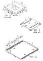
- FIG. 3 ais a drawing of the drop-in environmental control material carrier assembly 30 of this invention.
- the carrier assemblyis sized to drop into the cavity of a particular semiconductor package.
- the framehas four slots 301 - 304 , as shown, although additional slots could be added if required.
- the environmental control material 31 , 32is held in the slots 301 - 304 .
- half of thesetypically hold desiccants to absorb moisture and/or adhesive outgassing constituents and the remaining slots ( 302 and 304 ) hold PFDA lubricant reservoirs.
- the inside walls of the frame 30are cut down at both the top 305 and bottom 306 of each slot to provide a transportation path for the traces of lubricant and/or moisture to and from the micromirror, respectively.
- FIG. 3 bshows an exploded view of the slots 301 - 304 . These slots contain mesh structures 3010 - 3040 , which are used to hold the getters in place.
- FIG. 3 cshows slot 303 with its mesh 3030 on a larger scale.
- FIG. 4is a drawing showing one example of how the carrier assembly is fabricated in large quantities on lead-frames 40 to provide an effective, low-cost getter approach.
- the lead-frame 40will contain several carrier assemblies 41 - 43 (three shown). Each carrier assembly is attached by means of tabs 401 , which are cut to remove the piece-parts from the lead-frame 40 .
- Each carrier assemblycontains the appropriate number of slots 430 - 431 (two labeled), each w-th the built-in mesh to hold the environmental control material in place.
- FIG. 5is a cross-section of a semiconductor package outfitted with the carrier assembly of this invention.
- the packageis comprised of a substrate 50 with chip cavity 52 , a semiconductor chip 51 , bonding wires 53 , the carrier assembly 54 and environmental control materials 55 of this invention, and a top cover 56 .
- An adhesive 58typically is used to mount the carrier assembly in place inside the package cavity 52 , providing a thermal path between the carrier assembly 54 and package substrate 50 .
- an adhesive 57typically is used to attach the top cover 56 to the molded package (substrate and case) 50 .
- the inside walls of the carrier assembly 54are shown cut down in the areas of the carrier assembly slots to provide a path 59 above and below the carrier assembly for the appropriate gasses to flow.
- FIG. 6is a cross-sectional drawing of a package outfitted with the drop-in environmental control material carrier assembly of this invention, where the chip 61 is a micromirror device and the package's top lid 69 is a glass cover.
- the carrier assemblycan be fitted with a combination environmental control materials 65 , often up to eight material deposits, comprised of those that store PFDA lubricant and those that absorb moisture and/or adhesive outgassing constituents.
- the packageis comprised of a substrate 60 , a micromirror chip 61 mounted in the cavity 62 of the package, bond wires 63 , the drop in carrier assembly 64 and materials 65 of this invention, a drop-in aperture 66 with aperture opening 67 of cross-referenced patent application TI-26268, and a top cover glass 69 .
- Both the drop-in environmental control material carrier assembly 64 and drop-in aperture 66are attached to the package substrate 60 with an adhesive 68 .
- the cover glass 69is also attached to the package with an adhesive 70 . Since the environmental control materials are no longer mounted on the cover glass 69 , there is room to make the adhesive surface 70 wider, thereby improving the resistance of the package to moisture.
- This viewshows the gap 71 between the drop in aperture 66 and the cover glass 69 , which can be made large by adjusting the height of the package wall to move the glass cover out of the plane of the micromirror. Since the cover is not near the plane of the micromirror, optical defects in the cover are less likely to be visible in the projected image. Also shown is the open path 71 , for gasses and moisture to flow to and from the micromirror, where some of the environmental control materials absorb moisture and adhesive outgassing and others supply lubrication to the micromirror superstructure, thereby preventing sticking of mirrors.
- FIG. 7is a system level block diagram for a single-micromirror projection display system, which uses the improved micromirror package of this invention.
- the systemis comprised of a light source 70 , a first condenser lens 71 , a motor/color filter wheel assembly 72 , a second condenser lens 73 , a micromirror 74 in the improved package of this invention with drop-in environmental control material carrier assembly and optionally a drop-in aperture, a projection lens 75 , and a viewing screen 76 .
- FIG. 8Another example including a high-brightness micromirror projection display, which uses three micromirrors in the improved packages of this invention, is shown in FIG. 8.
- This systemis comprised of a lamp (light source) and reflector assembly 80 , a condenser lens 81 , a turning mirror 82 , a total internal reflective prism 83 , three micromirrors 84 (for red, green, and blue light) in the package of this invention with drop-in environmental control material carrier assembly and optionally a drop-in aperture, color splitting/color combining prisms 85 , a projection lens 86 , and a viewing screen 87 .
- drop-in environmental control material carrier assemblyholds various types of getter material, such as moisture absorption, adhesive outgassing absorption, and PFDA lubricant storage,
Landscapes
- Engineering & Computer Science (AREA)
- Microelectronics & Electronic Packaging (AREA)
- Computer Hardware Design (AREA)
- Physics & Mathematics (AREA)
- Condensed Matter Physics & Semiconductors (AREA)
- General Physics & Mathematics (AREA)
- Power Engineering (AREA)
- Mechanical Light Control Or Optical Switches (AREA)
- Projection Apparatus (AREA)
Abstract
Description
- This invention is related to concurrently filed U.S. Patent Applications bearing Attorney Docket No. TI-26268 entitled “Electro-Optical Package with Drop-in Aperture,” TI-28482 entitled “Enclosure for MEMS Device,” and U.S. Pat. No. 5,331,454 titled “Low Reset Voltage Process for DMD,” the contents of which are hereby incorporated by reference in this application.[0001]
- 1. Field of the Invention[0002]
- The present invention relates to the packaging of semiconductor devices and particularly to that of micromechanical devices.[0003]
- 2. Description of the Related Art[0004]
- Packaging is a critical part of producing high-performance semiconductor devices, particularly micro-electrical mechanical systems (MEMS) such as micromirror devices. Environment is a critical parameter for most semiconductor chips. For example, in a micromirror device, which is a particular variety of spatial light modulator, the mirrors land on the substrate surface of the device. In order to avoid the mirrors from sticking, it is necessary that the micromirror device is lubricated and packaged in an environment with minimal amounts of moisture, adhesives, dust, and other contaminants. It is shown in U.S. Pat. No. 5,331,454, titled “Low Reset Voltage Process for DMD,” that lubrication of the surface of the micromirrors landing electrodes with an oriented monolayer, such as Perfluordecanoic Acid (PFDA), can decrease the Van der Waals forces and thereby reduce the tendency for the mirrors to stick to the landing electrodes. It is also Know that water of the surface of the micromirror increases the tendency of the mirrors to stick.[0005]
- The packaging of micromirror chips for use in protection displays and other electro-optical applications has continued to present a cost barrier that contributes to higher priced projection display products. These packages are not only expensive, but also require a low throughput process that increases the product cycle time, thereby further driving up the cost.[0006]
- FIG. 1 shows a typical micromirror package. In the past, this has often been a hermetic package, although lower-cost plastic packages have been disclosed.[0007]
- The illustrated package is comprised of a[0008]
ceramic case 10 and an optical cover glass (lid)11. Thecover glass 11 has anaperture 110 through alight shield 120 deposited on the bottom side of thecover 11. Thecover 11 is attached to thepackage case 10 by either welding or adhesive techniques. The primary purpose of thelight shield 120 is to prevent stray light from reaching the bond wires and bond pads around the peripheral of the micromirror. These regions reflect stray light reaching them and the reflected light enters the projection optics of the display system, lowering the contrast ratio of the projected image. Packages housing non-electro-optical devices use opaque top covers11. - The environment inside these chip packages can be largely controlled by means of getters. FIG. 2 shows a micromirror package's[0009]
top cover 20 withgetter material 21 attached to the bottom surface to absorb moisture inside the package. Thegetter strips 21 are attached to thecover 20 with an adhesive22. - There is a need for an improved method of placing and holding a getter and other environmental control materials in a semiconductor package. The invention disclosed herein addresses these needs by moving the getter from the package cover and providing a low-cost drop-in environmental control material carrier assembly, which holds various kinds of environmental control materials material.[0010]
- SUMMARY OF THE INVENTION[0011]
- This invention discloses an improved semiconductor package with a drop-in environmental control material carrier assembly that provides higher-performance, lower-cost, and longer-life devices. The disclosed approach separates the getter material from the package's top cover and positions it in the package's cavity by means of a drop-in environmental control material carrier assembly.[0012]
- The environmental control material carrier assembly can hold various types of material and is in thermal contact with the package substrate walls. For example, in the case where the chip is a micromirror device, the frame will typically hold three types of materials; (1) a desiccant for absorbing moisture, (2) a getter for absorbing adhesive outgassing constituents, and (3) a reservoir of PFDA lubricant. This provides higher environmental control material capacity which results in overall higher performance and longer life micromirror devices.[0013]
- Potential advantages provided by the disclosed invention may include:[0014]
- 1. the package is made up of lower cost piece parts[0015]
- 2. offers multi-material functionality (moisture absorption, adhesive outgassing absorption, and lubricant storage) capability,[0016]
- 3. provides higher environmental control material capacity, and[0017]
- 4. provides an easier assembly process which results in lower cost devices.[0018]
- The included drawings are as follows:[0019]
- FIG. 1 is a drawing of a conventional micromirror package of the prior art having a glass cover with deposited metal light shield and etched aperture.[0020]
- FIG. 2 is a drawing showing a prior art getter attached to the underside of the package's top cover with an adhesive.[0021]
- FIG. 3[0022]aa is a drawing of the drop-in environmental control material carrier assembly according to one embodiment of this invention.
- FIG. 3[0023]bis a drawing showing the mesh structures that hold the environmental control materials in the carrier assembly of FIG. 3a.
- FIG. 3[0024]cis an exploded view of the mesh pattern of FIG. 3b.
- FIG. 4 is a drawing of a low-cost lead-frame used in providing the drop-in environmental control material carrier assembly of this invention.[0025]
- FIG. 5 is a cross-sectional drawing showing an example of a semiconductor package containing the drop-in environmental control material carrier assembly of this invention.[0026]
- FIG. 6 is a cross-sectional drawing showing an example of a micromirror package, which contains both the drop-in environmental control material carrier assembly of this invention and a drop-in aperture.[0027]
- FIG. 7 is block diagram of a single-micromirror projection system using the improved micromirror package, with drop-in environmental control material carrier assembly, of this invention.[0028]
- FIG. 8 is a block diagram of a high-brightness, three micromirror projection display system using the improved micromirror package, with drop-in environmental control material carrier assembly, of this invention.[0029]
- This invention discloses an improved semiconductor package with a drop-in environmental control material carrier assembly that provides higher-performance, lower-cost, and longer-life devices. The disclosed approach separates the environmental control material from the package's top cover and positions it in the package's cavity by means of a drop-in environmental control material carrier assembly. The approach of this invention increases the lifetime of a micromirror device, packaged in a non-hermetically sealed package, by increasing the moisture and adhesive outgassing absorption capacity and simultaneously lubricating the micromirror superstructure. The net result of this approach is overall higher performance and longer lifetime micromirrors.[0030]
- The carrier assembly of this invention can hold various combinations of environmental control material, for example; (1) a desiccant for absorbing moisture, (2) a desiccant for absorbing adhesive outgassing constituents, and (3) a lubricant reservoir in a micromirror package.[0031]
- Removing the environmental control material from the cover glass frees up space to provide a wider epoxy bond seal where the glass cover attaches to the package substrate walls, thereby decreasing the package's permeability and extending the device's life cycle.[0032]
- FIG. 3[0033]ais a drawing of the drop-in environmental control
material carrier assembly 30 of this invention. The carrier assembly is sized to drop into the cavity of a particular semiconductor package. The frame has four slots301-304, as shown, although additional slots could be added if required. Theenvironmental control material frame 30. In the particular case of a micromirror package, half of these (for example,slots 301 and303) typically hold desiccants to absorb moisture and/or adhesive outgassing constituents and the remaining slots (302 and304) hold PFDA lubricant reservoirs. The inside walls of theframe 30 are cut down at both the top305 andbottom 306 of each slot to provide a transportation path for the traces of lubricant and/or moisture to and from the micromirror, respectively. - FIG. 3[0034]bshows an exploded view of the slots301-304. These slots contain mesh structures3010-3040, which are used to hold the getters in place. FIG. 3cshows
slot 303 with itsmesh 3030 on a larger scale. - FIG. 4 is a drawing showing one example of how the carrier assembly is fabricated in large quantities on lead-[0035]
frames 40 to provide an effective, low-cost getter approach. The lead-frame 40 will contain several carrier assemblies41-43 (three shown). Each carrier assembly is attached by means oftabs 401, which are cut to remove the piece-parts from the lead-frame 40. Each carrier assembly contains the appropriate number of slots430-431 (two labeled), each w-th the built-in mesh to hold the environmental control material in place. - FIG. 5 is a cross-section of a semiconductor package outfitted with the carrier assembly of this invention. The package is comprised of a[0036]
substrate 50 withchip cavity 52, asemiconductor chip 51,bonding wires 53, thecarrier assembly 54 andenvironmental control materials 55 of this invention, and atop cover 56. An adhesive58 typically is used to mount the carrier assembly in place inside thepackage cavity 52, providing a thermal path between thecarrier assembly 54 andpackage substrate 50. Additionally, an adhesive57 typically is used to attach thetop cover 56 to the molded package (substrate and case)50. The inside walls of thecarrier assembly 54 are shown cut down in the areas of the carrier assembly slots to provide apath 59 above and below the carrier assembly for the appropriate gasses to flow. - FIG. 6 is a cross-sectional drawing of a package outfitted with the drop-in environmental control material carrier assembly of this invention, where the[0037]
chip 61 is a micromirror device and the package'stop lid 69 is a glass cover. In this case the carrier assembly can be fitted with a combinationenvironmental control materials 65, often up to eight material deposits, comprised of those that store PFDA lubricant and those that absorb moisture and/or adhesive outgassing constituents. The package is comprised of asubstrate 60, amicromirror chip 61 mounted in thecavity 62 of the package,bond wires 63, the drop incarrier assembly 64 andmaterials 65 of this invention, a drop-inaperture 66 withaperture opening 67 of cross-referenced patent application TI-26268, and atop cover glass 69. Both the drop-in environmental controlmaterial carrier assembly 64 and drop-inaperture 66 are attached to thepackage substrate 60 with an adhesive68. Thecover glass 69 is also attached to the package with an adhesive70. Since the environmental control materials are no longer mounted on thecover glass 69, there is room to make theadhesive surface 70 wider, thereby improving the resistance of the package to moisture. This view shows thegap 71 between the drop inaperture 66 and thecover glass 69, which can be made large by adjusting the height of the package wall to move the glass cover out of the plane of the micromirror. Since the cover is not near the plane of the micromirror, optical defects in the cover are less likely to be visible in the projected image. Also shown is theopen path 71, for gasses and moisture to flow to and from the micromirror, where some of the environmental control materials absorb moisture and adhesive outgassing and others supply lubrication to the micromirror superstructure, thereby preventing sticking of mirrors. - FIG. 7 is a system level block diagram for a single-micromirror projection display system, which uses the improved micromirror package of this invention. The system is comprised of a[0038]
light source 70, afirst condenser lens 71, a motor/colorfilter wheel assembly 72, asecond condenser lens 73, amicromirror 74 in the improved package of this invention with drop-in environmental control material carrier assembly and optionally a drop-in aperture, aprojection lens 75, and aviewing screen 76. - Another example including a high-brightness micromirror projection display, which uses three micromirrors in the improved packages of this invention, is shown in FIG. 8. This system is comprised of a lamp (light source) and[0039]
reflector assembly 80, acondenser lens 81, a turningmirror 82, a total internalreflective prism 83, three micromirrors84 (for red, green, and blue light) in the package of this invention with drop-in environmental control material carrier assembly and optionally a drop-in aperture, color splitting/color combining prisms 85, a projection lens86, and aviewing screen 87. - The improvements to the MEMS package of this invention considerably enhance the performance and lifetime and lowers the cost of such projection display systems. Some of the features potentially, but not necessarily provided by the disclosed invention are;[0040]
- 1. simpler package cover design,[0041]
- 2. improved cover alignment tolerance,[0042]
- 3. drop-in environmental control material carrier assembly holds various types of getter material, such as moisture absorption, adhesive outgassing absorption, and PFDA lubricant storage,[0043]
- 4. higher environmental control material capacity,[0044]
- 5. increased glass to substrate adhesive bond line width to increase moisture resistance, and[0045]
- 6. one size carrier assembly fits multiple packages, lowering inventory requirements and package cost.[0046]
- While this invention has been described in the context of preferred embodiments, it will be apparent to those skilled in the art that the present invention may be modified in numerous ways and may assume embodiments other than that specifically set out and described above. Accordingly, it is intended by the appended claims to cover all modifications of the invention that fall within the true spirit and scope of the invention.[0047]
Claims (21)
1. A semiconductor package, comprising:
a substrate;
a semiconductor device supported by said substrate;
a environmental control materials carrier assembly supported by said substrate; and
a top cover supported by said substrate to enclose said semiconductor device and said environmental control materials carrier assembly.
2. The semiconductor package ofclaim 1 , said environmental control material carrier assembly secured to said substrate by means of an adhesive.
3. The semiconductor package of claim i, said environmental control material carrier assembly further comprising:
a frame having at least two slots; and
environmental control material mounted in at least one of said slots.
4. The semiconductor package ofclaim 3 , said environmental control material carrier assembly frame having inside structural walls with openings to provide paths for gases and/or liquids inside said package to flow between said semiconductor chip and said getter material.
5. The semiconductor package ofclaim 3 , said slots having mesh structures for holding said environmental control material.
6. The semiconductor package ofclaim 3 , said environmental control material carrier assembly fabricated in a lead-frame with break away tabs attaching each said carrier assembly to said lead-frame.
7. The semiconductor package ofclaim 3 , said environmental control material comprising moisture-collecting desiccants.
8. The semiconductor package ofclaim 3 , said environmental control material comprising adhesive outgassing desiccants.
9. The semiconductor package ofclaim 3 , said environmental control material comprising lubricant storage reservoirs.
10. The semiconductor package ofclaim 3 , said environmental control material comprised of a combination of:
moisture collecting desiccants;
adhesive outgassing absorbing desiccants; and
lubricant storage reservoirs.
11. The semiconductor package ofclaim 1 , said semiconductor device comprising a spatial light modulator.
12. The semiconductor package ofclaim 11 , said spatial light modulator comprising a micromirror.
13. The semiconductor package ofclaim 1 , further comprising an aperture having a peripheral opaque light shield area and a center aperture area.
14. The semiconductor package ofclaim 13 , wherein said aperture is separate from said cover glass.
15. The semiconductor package ofclaim 13 , said aperture located to prevent light from reaching surfaces around a perimeter of semiconductor device.
16. The semiconductor package ofclaim 1 wherein said cover is glass with an anti-reflective coating.
17. A micromirror projection display comprising:
a light source for producing a beam of light traveling along a light path;
a micromirror for selectively modulating said beam of light, said micromirror mounted on said light bath in a package with a transparent window and a carrier assembly holding at least one environmental control material; and
a projection lens focusing said selectively modulated beam of light onto an image plane.
18. The micromirror projection display ofclaim 17 , said environmental control material comprising at least one environmental control material selected from the group consisting of water absorbing desiccants, adhesive outgassing desiccants, and lubricant storage reservoirs.
19. The micromirror projection display ofclaim 17 , said environmental control material comprising a desiccant for collecting moisture in said micromirror package.
20. The micromirror projection display ofclaim 17 , said environmental control material comprising a desiccant for collecting outgassed matter in said micromirror package.
21. The micromirror projection display ofclaim 17 , said environmental control material comprising a lubricant reservoir providing lubricant to said micromirror.
Priority Applications (1)
| Application Number | Priority Date | Filing Date | Title |
|---|---|---|---|
| US10/674,829US6879147B2 (en) | 2000-11-16 | 2003-09-30 | Package with environmental control material carrier |
Applications Claiming Priority (3)
| Application Number | Priority Date | Filing Date | Title |
|---|---|---|---|
| US24915000P | 2000-11-16 | 2000-11-16 | |
| US09/992,178US6664779B2 (en) | 2000-11-16 | 2001-11-05 | Package with environmental control material carrier |
| US10/674,829US6879147B2 (en) | 2000-11-16 | 2003-09-30 | Package with environmental control material carrier |
Related Parent Applications (1)
| Application Number | Title | Priority Date | Filing Date |
|---|---|---|---|
| US09/992,178DivisionUS6664779B2 (en) | 2000-11-16 | 2001-11-05 | Package with environmental control material carrier |
Publications (2)
| Publication Number | Publication Date |
|---|---|
| US20040061492A1true US20040061492A1 (en) | 2004-04-01 |
| US6879147B2 US6879147B2 (en) | 2005-04-12 |
Family
ID=26939866
Family Applications (2)
| Application Number | Title | Priority Date | Filing Date |
|---|---|---|---|
| US09/992,178Expired - LifetimeUS6664779B2 (en) | 2000-11-16 | 2001-11-05 | Package with environmental control material carrier |
| US10/674,829Expired - LifetimeUS6879147B2 (en) | 2000-11-16 | 2003-09-30 | Package with environmental control material carrier |
Family Applications Before (1)
| Application Number | Title | Priority Date | Filing Date |
|---|---|---|---|
| US09/992,178Expired - LifetimeUS6664779B2 (en) | 2000-11-16 | 2001-11-05 | Package with environmental control material carrier |
Country Status (1)
| Country | Link |
|---|---|
| US (2) | US6664779B2 (en) |
Cited By (33)
| Publication number | Priority date | Publication date | Assignee | Title |
|---|---|---|---|---|
| US20050035699A1 (en)* | 2003-08-15 | 2005-02-17 | Hsiung-Kuang Tsai | Optical interference display panel |
| US20050042117A1 (en)* | 2003-08-18 | 2005-02-24 | Wen-Jian Lin | Optical interference display panel and manufacturing method thereof |
| US20050237598A1 (en)* | 2000-12-29 | 2005-10-27 | Malone Joshua J | Laminated package |
| US20050254115A1 (en)* | 2004-05-12 | 2005-11-17 | Iridigm Display Corporation | Packaging for an interferometric modulator |
| US20060066600A1 (en)* | 2004-09-27 | 2006-03-30 | Lauren Palmateer | System and method for display device with reinforcing substance |
| US20060067647A1 (en)* | 2004-09-27 | 2006-03-30 | Clarence Chui | Method and system for maintaining partial vacuum in display device |
| US20060076632A1 (en)* | 2004-09-27 | 2006-04-13 | Lauren Palmateer | System and method for display device with activated desiccant |
| US20060077524A1 (en)* | 2004-09-27 | 2006-04-13 | Lauren Palmateer | System and method for display device with end-of-life phenomena |
| US20060077150A1 (en)* | 2004-09-27 | 2006-04-13 | Sampsell Jeffrey B | System and method of providing a regenerating protective coating in a MEMS device |
| US20060076648A1 (en)* | 2004-09-27 | 2006-04-13 | Brian Gally | System and method for protecting microelectromechanical systems array using structurally reinforced back-plate |
| US20060076631A1 (en)* | 2004-09-27 | 2006-04-13 | Lauren Palmateer | Method and system for providing MEMS device package with secondary seal |
| US20060077147A1 (en)* | 2004-09-27 | 2006-04-13 | Lauren Palmateer | System and method for protecting micro-structure of display array using spacers in gap within display device |
| US20060077503A1 (en)* | 2004-09-27 | 2006-04-13 | Lauren Palmateer | System and method of providing MEMS device with anti-stiction coating |
| US20060077146A1 (en)* | 2004-09-27 | 2006-04-13 | Lauren Palmateer | System and method for display device with integrated desiccant |
| US20060077533A1 (en)* | 2004-09-27 | 2006-04-13 | Miles Mark W | Method and system for packaging a MEMS device |
| US20060219435A1 (en)* | 2004-05-04 | 2006-10-05 | Manish Kothari | Modifying the electro-mechanical behavior of devices |
| US20070139655A1 (en)* | 2005-12-20 | 2007-06-21 | Qi Luo | Method and apparatus for reducing back-glass deflection in an interferometric modulator display device |
| US7259449B2 (en) | 2004-09-27 | 2007-08-21 | Idc, Llc | Method and system for sealing a substrate |
| US20070242341A1 (en)* | 2006-04-13 | 2007-10-18 | Qualcomm Incorporated | Mems devices and processes for packaging such devices |
| US20070268581A1 (en)* | 2006-05-17 | 2007-11-22 | Qualcomm Incorporated | Desiccant in a mems device |
| US20070297037A1 (en)* | 2006-06-21 | 2007-12-27 | Qualcomm Incorporated | Mems device having a recessed cavity and methods therefor |
| US7368803B2 (en) | 2004-09-27 | 2008-05-06 | Idc, Llc | System and method for protecting microelectromechanical systems array using back-plate with non-flat portion |
| US20080130082A1 (en)* | 2006-12-01 | 2008-06-05 | Qualcomm Mems Technologies, Inc. | Mems processing |
| US7424198B2 (en) | 2004-09-27 | 2008-09-09 | Idc, Llc | Method and device for packaging a substrate |
| US20090323170A1 (en)* | 2008-06-30 | 2009-12-31 | Qualcomm Mems Technologies, Inc. | Groove on cover plate or substrate |
| US20100020382A1 (en)* | 2008-07-22 | 2010-01-28 | Qualcomm Mems Technologies, Inc. | Spacer for mems device |
| US7668415B2 (en) | 2004-09-27 | 2010-02-23 | Qualcomm Mems Technologies, Inc. | Method and device for providing electronic circuitry on a backplate |
| US7701631B2 (en) | 2004-09-27 | 2010-04-20 | Qualcomm Mems Technologies, Inc. | Device having patterned spacers for backplates and method of making the same |
| US20100206629A1 (en)* | 2009-02-13 | 2010-08-19 | Qualcomm Mems Technologies, Inc. | Display device with desiccant |
| US20110012219A1 (en)* | 2007-09-28 | 2011-01-20 | Qualcomm Mems Technologies, Inc. | Optimization of desiccant usage in a mems package |
| US20110096508A1 (en)* | 2009-10-23 | 2011-04-28 | Qualcomm Mems Technologies, Inc. | Light-based sealing and device packaging |
| US8124434B2 (en) | 2004-09-27 | 2012-02-28 | Qualcomm Mems Technologies, Inc. | Method and system for packaging a display |
| US8735225B2 (en) | 2004-09-27 | 2014-05-27 | Qualcomm Mems Technologies, Inc. | Method and system for packaging MEMS devices with glass seal |
Families Citing this family (40)
| Publication number | Priority date | Publication date | Assignee | Title |
|---|---|---|---|---|
| US6589625B1 (en) | 2001-08-01 | 2003-07-08 | Iridigm Display Corporation | Hermetic seal and method to create the same |
| US7764950B2 (en)* | 2002-05-24 | 2010-07-27 | Kodiak Networks, Inc. | Advanced voice services architecture framework |
| US7259505B2 (en)* | 2002-10-15 | 2007-08-21 | Eastman Kodak Company | OLED display with circular polarizer |
| US7417782B2 (en)* | 2005-02-23 | 2008-08-26 | Pixtronix, Incorporated | Methods and apparatus for spatial light modulation |
| US8619352B2 (en)* | 2003-07-29 | 2013-12-31 | Silicon Quest Kabushiki-Kaisha | Projection display system using laser light source |
| US8194305B2 (en)* | 2003-11-01 | 2012-06-05 | Silicon Quest Kabushiki-Kaisha | Package for micromirror device |
| US20060007515A1 (en)* | 2003-11-13 | 2006-01-12 | Dmitri Simonian | Surface lubrication in microstructures |
| US7109580B2 (en)* | 2004-03-03 | 2006-09-19 | Hymite A/S | Hermetically sealed package for optical, electronic, opto-electronic and other devices |
| US20050212067A1 (en)* | 2004-03-26 | 2005-09-29 | Robert Duboc | Microelectromechanical devices with lubricants and getters formed thereon |
| US6979893B2 (en)* | 2004-03-26 | 2005-12-27 | Reflectivity, Inc | Packaged microelectromechanical device with lubricant |
| US7307773B2 (en)* | 2005-01-04 | 2007-12-11 | Hewlett-Packard Development Company, L.P. | Micro-optoelectromechanical system packages for a light modulator and methods of making the same |
| US9082353B2 (en) | 2010-01-05 | 2015-07-14 | Pixtronix, Inc. | Circuits for controlling display apparatus |
| US7999994B2 (en) | 2005-02-23 | 2011-08-16 | Pixtronix, Inc. | Display apparatus and methods for manufacture thereof |
| US8482496B2 (en) | 2006-01-06 | 2013-07-09 | Pixtronix, Inc. | Circuits for controlling MEMS display apparatus on a transparent substrate |
| US9158106B2 (en) | 2005-02-23 | 2015-10-13 | Pixtronix, Inc. | Display methods and apparatus |
| US20070205969A1 (en) | 2005-02-23 | 2007-09-06 | Pixtronix, Incorporated | Direct-view MEMS display devices and methods for generating images thereon |
| US9087486B2 (en) | 2005-02-23 | 2015-07-21 | Pixtronix, Inc. | Circuits for controlling display apparatus |
| US9261694B2 (en) | 2005-02-23 | 2016-02-16 | Pixtronix, Inc. | Display apparatus and methods for manufacture thereof |
| US7304786B2 (en) | 2005-02-23 | 2007-12-04 | Pixtronix, Inc. | Methods and apparatus for bi-stable actuation of displays |
| US8159428B2 (en) | 2005-02-23 | 2012-04-17 | Pixtronix, Inc. | Display methods and apparatus |
| US8310442B2 (en) | 2005-02-23 | 2012-11-13 | Pixtronix, Inc. | Circuits for controlling display apparatus |
| US20080158635A1 (en)* | 2005-02-23 | 2008-07-03 | Pixtronix, Inc. | Display apparatus and methods for manufacture thereof |
| US7502159B2 (en)* | 2005-02-23 | 2009-03-10 | Pixtronix, Inc. | Methods and apparatus for actuating displays |
| US7304785B2 (en)* | 2005-02-23 | 2007-12-04 | Pixtronix, Inc. | Display methods and apparatus |
| US8519945B2 (en) | 2006-01-06 | 2013-08-27 | Pixtronix, Inc. | Circuits for controlling display apparatus |
| US9229222B2 (en) | 2005-02-23 | 2016-01-05 | Pixtronix, Inc. | Alignment methods in fluid-filled MEMS displays |
| US7348193B2 (en)* | 2005-06-30 | 2008-03-25 | Corning Incorporated | Hermetic seals for micro-electromechanical system devices |
| US7417307B2 (en)* | 2005-07-29 | 2008-08-26 | Hewlett-Packard Development Company, L.P. | System and method for direct-bonding of substrates |
| US7723812B2 (en)* | 2005-11-23 | 2010-05-25 | Miradia, Inc. | Preferentially deposited lubricant to prevent anti-stiction in micromechanical systems |
| US8526096B2 (en) | 2006-02-23 | 2013-09-03 | Pixtronix, Inc. | Mechanical light modulators with stressed beams |
| US9176318B2 (en) | 2007-05-18 | 2015-11-03 | Pixtronix, Inc. | Methods for manufacturing fluid-filled MEMS displays |
| GB2451921A (en)* | 2007-08-17 | 2009-02-18 | Wolfson Microelectronics Plc | MEMS package |
| GB2451908B (en)* | 2007-08-17 | 2009-12-02 | Wolfson Microelectronics Plc | Mems package |
| FR2933389B1 (en)* | 2008-07-01 | 2010-10-29 | Commissariat Energie Atomique | STRUCTURE BASED ON SUSPENDED GETTER MATERIAL |
| US8169679B2 (en) | 2008-10-27 | 2012-05-01 | Pixtronix, Inc. | MEMS anchors |
| KR20120132680A (en) | 2010-02-02 | 2012-12-07 | 픽스트로닉스 인코포레이티드 | Methods for manufacturing cold seal fluid-filled display apparatus |
| FR2971083B1 (en) | 2011-02-02 | 2014-04-25 | Ulis | METHOD OF ASSEMBLING AND HERMETICALLY CLOSING AN ENCAPSULATION HOUSING |
| US8987871B2 (en)* | 2012-05-31 | 2015-03-24 | Stmicroelectronics Pte Ltd. | Cap for a microelectromechanical system device with electromagnetic shielding, and method of manufacture |
| US9134552B2 (en) | 2013-03-13 | 2015-09-15 | Pixtronix, Inc. | Display apparatus with narrow gap electrostatic actuators |
| CN113135550B (en)* | 2021-02-26 | 2021-12-21 | 欧梯恩智能科技(苏州)有限公司 | Photon sensing chip preparation method and photon sensing chip |
Citations (9)
| Publication number | Priority date | Publication date | Assignee | Title |
|---|---|---|---|---|
| US5331454A (en)* | 1990-11-13 | 1994-07-19 | Texas Instruments Incorporated | Low reset voltage process for DMD |
| US5517347A (en)* | 1993-12-01 | 1996-05-14 | Texas Instruments Incorporated | Direct view deformable mirror device |
| US5640479A (en)* | 1995-10-18 | 1997-06-17 | Palomar Technologies Corporation | Fiberoptic face plate stop for digital micromirror device projection system |
| US6024801A (en)* | 1995-05-31 | 2000-02-15 | Texas Instruments Incorporated | Method of cleaning and treating a semiconductor device including a micromechanical device |
| US6049825A (en)* | 1997-03-19 | 2000-04-11 | Fujitsu Limited | Method and system for switching between duplicated network interface adapters for host computer communications |
| US6242165B1 (en)* | 1998-08-28 | 2001-06-05 | Micron Technology, Inc. | Supercritical compositions for removal of organic material and methods of using same |
| US20020056900A1 (en)* | 2000-11-16 | 2002-05-16 | Liu Jwei Wien | Electro-optical package with drop-in aperture |
| US20020056560A1 (en)* | 2000-11-16 | 2002-05-16 | Liu Jwei Wien | MEMS enclosure |
| US20020107966A1 (en)* | 2001-02-06 | 2002-08-08 | Jacques Baudot | Method and system for maintaining connections in a network |
- 2001
- 2001-11-05USUS09/992,178patent/US6664779B2/ennot_activeExpired - Lifetime
- 2003
- 2003-09-30USUS10/674,829patent/US6879147B2/ennot_activeExpired - Lifetime
Patent Citations (9)
| Publication number | Priority date | Publication date | Assignee | Title |
|---|---|---|---|---|
| US5331454A (en)* | 1990-11-13 | 1994-07-19 | Texas Instruments Incorporated | Low reset voltage process for DMD |
| US5517347A (en)* | 1993-12-01 | 1996-05-14 | Texas Instruments Incorporated | Direct view deformable mirror device |
| US6024801A (en)* | 1995-05-31 | 2000-02-15 | Texas Instruments Incorporated | Method of cleaning and treating a semiconductor device including a micromechanical device |
| US5640479A (en)* | 1995-10-18 | 1997-06-17 | Palomar Technologies Corporation | Fiberoptic face plate stop for digital micromirror device projection system |
| US6049825A (en)* | 1997-03-19 | 2000-04-11 | Fujitsu Limited | Method and system for switching between duplicated network interface adapters for host computer communications |
| US6242165B1 (en)* | 1998-08-28 | 2001-06-05 | Micron Technology, Inc. | Supercritical compositions for removal of organic material and methods of using same |
| US20020056900A1 (en)* | 2000-11-16 | 2002-05-16 | Liu Jwei Wien | Electro-optical package with drop-in aperture |
| US20020056560A1 (en)* | 2000-11-16 | 2002-05-16 | Liu Jwei Wien | MEMS enclosure |
| US20020107966A1 (en)* | 2001-02-06 | 2002-08-08 | Jacques Baudot | Method and system for maintaining connections in a network |
Cited By (87)
| Publication number | Priority date | Publication date | Assignee | Title |
|---|---|---|---|---|
| US7345807B2 (en)* | 2000-12-29 | 2008-03-18 | Texas Instruments Incorporated | Laminated package |
| US20050237598A1 (en)* | 2000-12-29 | 2005-10-27 | Malone Joshua J | Laminated package |
| US8792179B2 (en) | 2000-12-29 | 2014-07-29 | Texas Instruments Incorporated | Laminated micromirror package |
| US20110058246A1 (en)* | 2000-12-29 | 2011-03-10 | Texas Instruments Incorported | Laminated Micromirror Package |
| US7843643B2 (en) | 2000-12-29 | 2010-11-30 | Texas Instruments Incorporated | Laminated micromirror package |
| US7307776B2 (en) | 2003-08-15 | 2007-12-11 | Qualcomm Incorporated | Optical interference display panel |
| US7470373B2 (en) | 2003-08-15 | 2008-12-30 | Qualcomm Mems Technologies, Inc. | Optical interference display panel |
| US20090103167A1 (en)* | 2003-08-15 | 2009-04-23 | Qualcomm Mems Technologies, Inc. | Optical interference display panel |
| US20060148365A1 (en)* | 2003-08-15 | 2006-07-06 | Hsiung-Kuang Tsai | Optical interference display panel |
| US7978396B2 (en) | 2003-08-15 | 2011-07-12 | Qualcomm Mems Technologies, Inc. | Optical interference display panel |
| US20050035699A1 (en)* | 2003-08-15 | 2005-02-17 | Hsiung-Kuang Tsai | Optical interference display panel |
| US20090219605A1 (en)* | 2003-08-18 | 2009-09-03 | Qualcomm Mems Technologies, Inc | Optical interference display panel and manufacturing method thereof |
| US7532385B2 (en) | 2003-08-18 | 2009-05-12 | Qualcomm Mems Technologies, Inc. | Optical interference display panel and manufacturing method thereof |
| US8004736B2 (en) | 2003-08-18 | 2011-08-23 | Qualcomm Mems Technologies, Inc. | Optical interference display panel and manufacturing method thereof |
| US20050042117A1 (en)* | 2003-08-18 | 2005-02-24 | Wen-Jian Lin | Optical interference display panel and manufacturing method thereof |
| US20060219435A1 (en)* | 2004-05-04 | 2006-10-05 | Manish Kothari | Modifying the electro-mechanical behavior of devices |
| US7161094B2 (en) | 2004-05-04 | 2007-01-09 | Idc, Llc | Modifying the electro-mechanical behavior of devices |
| US7816710B2 (en) | 2004-05-12 | 2010-10-19 | Qualcomm Mems Technologies, Inc. | Packaging for an interferometric modulator with a curved back plate |
| US20110053304A1 (en)* | 2004-05-12 | 2011-03-03 | Qualcomm Mems Technologies, Inc. | Method of making an electronic device with a curved backplate |
| US7164520B2 (en) | 2004-05-12 | 2007-01-16 | Idc, Llc | Packaging for an interferometric modulator |
| US8853747B2 (en) | 2004-05-12 | 2014-10-07 | Qualcomm Mems Technologies, Inc. | Method of making an electronic device with a curved backplate |
| US20050254115A1 (en)* | 2004-05-12 | 2005-11-17 | Iridigm Display Corporation | Packaging for an interferometric modulator |
| US20070170568A1 (en)* | 2004-05-12 | 2007-07-26 | Lauren Palmateer | Packaging for an interferometric modulator |
| US7443563B2 (en) | 2004-05-12 | 2008-10-28 | Idc, Llc | Packaging for an interferometric modulator |
| US7550912B2 (en) | 2004-09-27 | 2009-06-23 | Idc, Llc | Method and system for maintaining partial vacuum in display device |
| US7710629B2 (en) | 2004-09-27 | 2010-05-04 | Qualcomm Mems Technologies, Inc. | System and method for display device with reinforcing substance |
| US20060066600A1 (en)* | 2004-09-27 | 2006-03-30 | Lauren Palmateer | System and method for display device with reinforcing substance |
| US20060067647A1 (en)* | 2004-09-27 | 2006-03-30 | Clarence Chui | Method and system for maintaining partial vacuum in display device |
| US20070298541A1 (en)* | 2004-09-27 | 2007-12-27 | Idc, Llc | Method and system for sealing a substrate |
| US8735225B2 (en) | 2004-09-27 | 2014-05-27 | Qualcomm Mems Technologies, Inc. | Method and system for packaging MEMS devices with glass seal |
| US8682130B2 (en) | 2004-09-27 | 2014-03-25 | Qualcomm Mems Technologies, Inc. | Method and device for packaging a substrate |
| US7368803B2 (en) | 2004-09-27 | 2008-05-06 | Idc, Llc | System and method for protecting microelectromechanical systems array using back-plate with non-flat portion |
| US8124434B2 (en) | 2004-09-27 | 2012-02-28 | Qualcomm Mems Technologies, Inc. | Method and system for packaging a display |
| US7405924B2 (en) | 2004-09-27 | 2008-07-29 | Idc, Llc | System and method for protecting microelectromechanical systems array using structurally reinforced back-plate |
| US7424198B2 (en) | 2004-09-27 | 2008-09-09 | Idc, Llc | Method and device for packaging a substrate |
| US7259449B2 (en) | 2004-09-27 | 2007-08-21 | Idc, Llc | Method and system for sealing a substrate |
| US7446926B2 (en) | 2004-09-27 | 2008-11-04 | Idc, Llc | System and method of providing a regenerating protective coating in a MEMS device |
| US8115983B2 (en) | 2004-09-27 | 2012-02-14 | Qualcomm Mems Technologies, Inc. | Method and system for packaging a MEMS device |
| US7518775B2 (en) | 2004-09-27 | 2009-04-14 | Idc, Llc | Method and system for packaging a MEMS device |
| US7184202B2 (en) | 2004-09-27 | 2007-02-27 | Idc, Llc | Method and system for packaging a MEMS device |
| US20060077533A1 (en)* | 2004-09-27 | 2006-04-13 | Miles Mark W | Method and system for packaging a MEMS device |
| US7551246B2 (en) | 2004-09-27 | 2009-06-23 | Idc, Llc. | System and method for display device with integrated desiccant |
| US20060077146A1 (en)* | 2004-09-27 | 2006-04-13 | Lauren Palmateer | System and method for display device with integrated desiccant |
| US8090229B2 (en) | 2004-09-27 | 2012-01-03 | Qualcomm Mems Technologies, Inc. | Method and device for providing electronic circuitry on a backplate |
| US7573547B2 (en) | 2004-09-27 | 2009-08-11 | Idc, Llc | System and method for protecting micro-structure of display array using spacers in gap within display device |
| US20060077503A1 (en)* | 2004-09-27 | 2006-04-13 | Lauren Palmateer | System and method of providing MEMS device with anti-stiction coating |
| US20090257109A1 (en)* | 2004-09-27 | 2009-10-15 | Idc, Llc | Method and system for packaging a mems device |
| US7629678B2 (en) | 2004-09-27 | 2009-12-08 | Qualcomm Mems Technologies, Inc. | Method and system for sealing a substrate |
| US8045835B2 (en) | 2004-09-27 | 2011-10-25 | Qualcomm Mems Technologies, Inc. | Method and device for packaging a substrate |
| US7642127B2 (en) | 2004-09-27 | 2010-01-05 | Qualcomm Mems Technologies, Inc. | Method and system for sealing a substrate |
| US20060076632A1 (en)* | 2004-09-27 | 2006-04-13 | Lauren Palmateer | System and method for display device with activated desiccant |
| US7668415B2 (en) | 2004-09-27 | 2010-02-23 | Qualcomm Mems Technologies, Inc. | Method and device for providing electronic circuitry on a backplate |
| US20100072595A1 (en)* | 2004-09-27 | 2010-03-25 | Qualcomm Mems Technologies, Inc. | Method and system for sealing a substrate |
| US7692839B2 (en) | 2004-09-27 | 2010-04-06 | Qualcomm Mems Technologies, Inc. | System and method of providing MEMS device with anti-stiction coating |
| US7701631B2 (en) | 2004-09-27 | 2010-04-20 | Qualcomm Mems Technologies, Inc. | Device having patterned spacers for backplates and method of making the same |
| US20070247693A1 (en)* | 2004-09-27 | 2007-10-25 | Idc, Llc | Method and system for packaging a mems device |
| US20110199668A1 (en)* | 2004-09-27 | 2011-08-18 | Qualcomm Mems Technologies, Inc. | Method and device for providing electronic circuitry on a backplate |
| US7990601B2 (en) | 2004-09-27 | 2011-08-02 | Qualcomm Mems Technologies, Inc. | System and method for display device with reinforcing substance |
| US20100172013A1 (en)* | 2004-09-27 | 2010-07-08 | Qualcomm Mems Technologies, Inc. | System and method for display device with reinforcing substance |
| US20060077524A1 (en)* | 2004-09-27 | 2006-04-13 | Lauren Palmateer | System and method for display device with end-of-life phenomena |
| US20060077147A1 (en)* | 2004-09-27 | 2006-04-13 | Lauren Palmateer | System and method for protecting micro-structure of display array using spacers in gap within display device |
| US7935555B2 (en) | 2004-09-27 | 2011-05-03 | Qualcomm Mems Technologies, Inc. | Method and system for sealing a substrate |
| US7933476B2 (en) | 2004-09-27 | 2011-04-26 | Qualcomm Mems Technologies, Inc. | Method and device for providing electronic circuitry on a backplate |
| US20060076631A1 (en)* | 2004-09-27 | 2006-04-13 | Lauren Palmateer | Method and system for providing MEMS device package with secondary seal |
| US7916103B2 (en) | 2004-09-27 | 2011-03-29 | Qualcomm Mems Technologies, Inc. | System and method for display device with end-of-life phenomena |
| US20060076648A1 (en)* | 2004-09-27 | 2006-04-13 | Brian Gally | System and method for protecting microelectromechanical systems array using structurally reinforced back-plate |
| US20060077150A1 (en)* | 2004-09-27 | 2006-04-13 | Sampsell Jeffrey B | System and method of providing a regenerating protective coating in a MEMS device |
| US7561334B2 (en) | 2005-12-20 | 2009-07-14 | Qualcomm Mems Technologies, Inc. | Method and apparatus for reducing back-glass deflection in an interferometric modulator display device |
| US20070139655A1 (en)* | 2005-12-20 | 2007-06-21 | Qi Luo | Method and apparatus for reducing back-glass deflection in an interferometric modulator display device |
| US7746537B2 (en) | 2006-04-13 | 2010-06-29 | Qualcomm Mems Technologies, Inc. | MEMS devices and processes for packaging such devices |
| US20070242345A1 (en)* | 2006-04-13 | 2007-10-18 | Qualcomm Incorporated | Packaging a mems device using a frame |
| US7715080B2 (en) | 2006-04-13 | 2010-05-11 | Qualcomm Mems Technologies, Inc. | Packaging a MEMS device using a frame |
| US20070242341A1 (en)* | 2006-04-13 | 2007-10-18 | Qualcomm Incorporated | Mems devices and processes for packaging such devices |
| US20070268581A1 (en)* | 2006-05-17 | 2007-11-22 | Qualcomm Incorporated | Desiccant in a mems device |
| US8040587B2 (en) | 2006-05-17 | 2011-10-18 | Qualcomm Mems Technologies, Inc. | Desiccant in a MEMS device |
| US20070297037A1 (en)* | 2006-06-21 | 2007-12-27 | Qualcomm Incorporated | Mems device having a recessed cavity and methods therefor |
| US7826127B2 (en) | 2006-06-21 | 2010-11-02 | Qualcomm Mems Technologies, Inc. | MEMS device having a recessed cavity and methods therefor |
| US20080130082A1 (en)* | 2006-12-01 | 2008-06-05 | Qualcomm Mems Technologies, Inc. | Mems processing |
| US7816164B2 (en) | 2006-12-01 | 2010-10-19 | Qualcomm Mems Technologies, Inc. | MEMS processing |
| US8435838B2 (en) | 2007-09-28 | 2013-05-07 | Qualcomm Mems Technologies, Inc. | Optimization of desiccant usage in a MEMS package |
| US20110012219A1 (en)* | 2007-09-28 | 2011-01-20 | Qualcomm Mems Technologies, Inc. | Optimization of desiccant usage in a mems package |
| US20090323170A1 (en)* | 2008-06-30 | 2009-12-31 | Qualcomm Mems Technologies, Inc. | Groove on cover plate or substrate |
| US20100020382A1 (en)* | 2008-07-22 | 2010-01-28 | Qualcomm Mems Technologies, Inc. | Spacer for mems device |
| US8410690B2 (en) | 2009-02-13 | 2013-04-02 | Qualcomm Mems Technologies, Inc. | Display device with desiccant |
| US20100206629A1 (en)* | 2009-02-13 | 2010-08-19 | Qualcomm Mems Technologies, Inc. | Display device with desiccant |
| US8379392B2 (en) | 2009-10-23 | 2013-02-19 | Qualcomm Mems Technologies, Inc. | Light-based sealing and device packaging |
| US20110096508A1 (en)* | 2009-10-23 | 2011-04-28 | Qualcomm Mems Technologies, Inc. | Light-based sealing and device packaging |
Also Published As
| Publication number | Publication date |
|---|---|
| US6664779B2 (en) | 2003-12-16 |
| US20020056898A1 (en) | 2002-05-16 |
| US6879147B2 (en) | 2005-04-12 |
Similar Documents
| Publication | Publication Date | Title |
|---|---|---|
| US6879147B2 (en) | Package with environmental control material carrier | |
| US6762868B2 (en) | Electro-optical package with drop-in aperture | |
| US6833942B2 (en) | MEMS enclosure | |
| JP2005062817A (en) | Optical interference display panel | |
| US7042623B1 (en) | Light blocking layers in MEMS packages | |
| US7449773B2 (en) | Microelectromechanical device packages with integral heaters | |
| US6300294B1 (en) | Lubricant delivery for micromechanical devices | |
| US6906847B2 (en) | Spatial light modulators with light blocking/absorbing areas | |
| US6843936B1 (en) | Getter for enhanced micromechanical device performance | |
| US20030002019A1 (en) | Lubricating micro-machined devices using fluorosurfactants | |
| US20080111203A1 (en) | Wafer-level packaging of micro devices | |
| JP2005062816A (en) | Optical interference type display panel | |
| EP2128905B1 (en) | Semiconductor light emitting device | |
| US7012315B1 (en) | Frame scale package using contact lines through the elements | |
| US7839560B2 (en) | Packaged spatial light modulator and a display system using the same | |
| US20080158519A1 (en) | Laminated Micromirror Package | |
| KR102340779B1 (en) | Lens assembly and camera module including the lens assembly | |
| WO2017110176A1 (en) | Optical element package | |
| JP7032634B2 (en) | Optical engine and projector | |
| US6827449B1 (en) | Adhesive-sealed window lid for micromechanical devices | |
| US7508132B2 (en) | Device having a getter structure and a photomask | |
| JP6940765B2 (en) | Light source device, optical engine and projector | |
| JP2016029432A (en) | Electro-optical device and electronic apparatus | |
| JPH10313147A (en) | Semiconductor laser light source | |
| US20230155073A1 (en) | Light-emitting diode (led) package with reflective coating and method of manufacture |
Legal Events
| Date | Code | Title | Description |
|---|---|---|---|
| STCF | Information on status: patent grant | Free format text:PATENTED CASE | |
| FPAY | Fee payment | Year of fee payment:4 | |
| FPAY | Fee payment | Year of fee payment:8 | |
| FPAY | Fee payment | Year of fee payment:12 |