US20040061447A1 - Method and apparatus for an improved upper electrode plate in a plasma processing system - Google Patents
Method and apparatus for an improved upper electrode plate in a plasma processing systemDownload PDFInfo
- Publication number
- US20040061447A1 US20040061447A1US10/259,757US25975702AUS2004061447A1US 20040061447 A1US20040061447 A1US 20040061447A1US 25975702 AUS25975702 AUS 25975702AUS 2004061447 A1US2004061447 A1US 2004061447A1
- Authority
- US
- United States
- Prior art keywords
- recited
- electrode plate
- exposed surfaces
- protective barrier
- electrode
- Prior art date
- Legal status (The legal status is an assumption and is not a legal conclusion. Google has not performed a legal analysis and makes no representation as to the accuracy of the status listed.)
- Granted
Links
- 238000012545processingMethods0.000titleclaimsabstractdescription121
- 238000000034methodMethods0.000titleclaimsabstractdescription100
- 238000002347injectionMethods0.000claimsabstractdescription53
- 239000007924injectionSubstances0.000claimsabstractdescription53
- 230000004888barrier functionEffects0.000claimsdescription52
- 230000001681protective effectEffects0.000claimsdescription52
- 238000002048anodisation reactionMethods0.000claimsdescription28
- 238000007789sealingMethods0.000claimsdescription24
- 238000003754machiningMethods0.000claimsdescription23
- 230000008878couplingEffects0.000claimsdescription20
- 238000010168coupling processMethods0.000claimsdescription20
- 238000005859coupling reactionMethods0.000claimsdescription20
- 230000013011matingEffects0.000claimsdescription17
- 238000005498polishingMethods0.000claimsdescription17
- RUDFQVOCFDJEEF-UHFFFAOYSA-Nyttrium(III) oxideInorganic materials[O-2].[O-2].[O-2].[Y+3].[Y+3]RUDFQVOCFDJEEF-UHFFFAOYSA-N0.000claimsdescription14
- 229910052782aluminiumInorganic materials0.000claimsdescription11
- XAGFODPZIPBFFR-UHFFFAOYSA-NaluminiumChemical compound[Al]XAGFODPZIPBFFR-UHFFFAOYSA-N0.000claimsdescription11
- 238000007743anodisingMethods0.000claimsdescription10
- 230000000873masking effectEffects0.000claimsdescription9
- 150000001875compoundsChemical class0.000claimsdescription8
- 238000005266castingMethods0.000claimsdescription7
- 238000005242forgingMethods0.000claimsdescription7
- 238000000227grindingMethods0.000claimsdescription7
- 230000002093peripheral effectEffects0.000claimsdescription7
- 229910052684CeriumInorganic materials0.000claimsdescription5
- 229910052692DysprosiumInorganic materials0.000claimsdescription5
- 229910052693EuropiumInorganic materials0.000claimsdescription5
- -1Sc2F3Inorganic materials0.000claimsdescription5
- 229910009527YF3Inorganic materials0.000claimsdescription5
- 230000015572biosynthetic processEffects0.000claimsdescription5
- CETPSERCERDGAM-UHFFFAOYSA-Nceric oxideChemical compoundO=[Ce]=OCETPSERCERDGAM-UHFFFAOYSA-N0.000claimsdescription5
- ZMIGMASIKSOYAM-UHFFFAOYSA-NceriumChemical compound[Ce][Ce][Ce][Ce][Ce][Ce][Ce][Ce][Ce][Ce][Ce][Ce][Ce][Ce][Ce][Ce][Ce][Ce][Ce][Ce][Ce][Ce][Ce][Ce][Ce][Ce][Ce][Ce][Ce][Ce][Ce][Ce][Ce][Ce][Ce][Ce][Ce][Ce]ZMIGMASIKSOYAM-UHFFFAOYSA-N0.000claimsdescription5
- 229910000422cerium(IV) oxideInorganic materials0.000claimsdescription5
- KBQHZAAAGSGFKK-UHFFFAOYSA-Ndysprosium atomChemical compound[Dy]KBQHZAAAGSGFKK-UHFFFAOYSA-N0.000claimsdescription5
- OGPBJKLSAFTDLK-UHFFFAOYSA-Neuropium atomChemical compound[Eu]OGPBJKLSAFTDLK-UHFFFAOYSA-N0.000claimsdescription5
- RSEIMSPAXMNYFJ-UHFFFAOYSA-Neuropium(III) oxideInorganic materialsO=[Eu]O[Eu]=ORSEIMSPAXMNYFJ-UHFFFAOYSA-N0.000claimsdescription5
- 229910052746lanthanumInorganic materials0.000claimsdescription5
- FZLIPJUXYLNCLC-UHFFFAOYSA-Nlanthanum atomChemical compound[La]FZLIPJUXYLNCLC-UHFFFAOYSA-N0.000claimsdescription5
- MRELNEQAGSRDBK-UHFFFAOYSA-Nlanthanum oxideInorganic materials[O-2].[O-2].[O-2].[La+3].[La+3]MRELNEQAGSRDBK-UHFFFAOYSA-N0.000claimsdescription5
- KTUFCUMIWABKDW-UHFFFAOYSA-Noxo(oxolanthaniooxy)lanthanumChemical compoundO=[La]O[La]=OKTUFCUMIWABKDW-UHFFFAOYSA-N0.000claimsdescription5
- 229910052706scandiumInorganic materials0.000claimsdescription5
- SIXSYDAISGFNSX-UHFFFAOYSA-Nscandium atomChemical compound[Sc]SIXSYDAISGFNSX-UHFFFAOYSA-N0.000claimsdescription5
- HYXGAEYDKFCVMU-UHFFFAOYSA-Nscandium(III) oxideInorganic materialsO=[Sc]O[Sc]=OHYXGAEYDKFCVMU-UHFFFAOYSA-N0.000claimsdescription5
- 229910052727yttriumInorganic materials0.000claimsdescription5
- VWQVUPCCIRVNHF-UHFFFAOYSA-Nyttrium atomChemical compound[Y]VWQVUPCCIRVNHF-UHFFFAOYSA-N0.000claimsdescription5
- 229910052751metalInorganic materials0.000claims4
- 239000002184metalSubstances0.000claims4
- 230000008569processEffects0.000abstractdescription14
- 238000004519manufacturing processMethods0.000abstractdescription6
- 238000013461designMethods0.000abstractdescription2
- 230000003628erosive effectEffects0.000abstractdescription2
- 239000000758substrateSubstances0.000description34
- 239000007789gasSubstances0.000description33
- 230000003287optical effectEffects0.000description16
- 230000008021depositionEffects0.000description12
- 239000010410layerSubstances0.000description12
- 238000005507sprayingMethods0.000description12
- 239000000463materialSubstances0.000description7
- TWNQGVIAIRXVLR-UHFFFAOYSA-Noxo(oxoalumanyloxy)alumaneChemical compoundO=[Al]O[Al]=OTWNQGVIAIRXVLR-UHFFFAOYSA-N0.000description7
- XKRFYHLGVUSROY-UHFFFAOYSA-NArgonChemical compound[Ar]XKRFYHLGVUSROY-UHFFFAOYSA-N0.000description4
- 238000010586diagramMethods0.000description4
- 238000010438heat treatmentMethods0.000description4
- 238000012546transferMethods0.000description4
- 244000137852Petrea volubilisSpecies0.000description3
- 239000000919ceramicSubstances0.000description3
- 238000007796conventional methodMethods0.000description3
- 239000000203mixtureSubstances0.000description3
- 229910052786argonInorganic materials0.000description2
- 150000002500ionsChemical class0.000description2
- 238000012423maintenanceMethods0.000description2
- 238000012986modificationMethods0.000description2
- 230000004048modificationEffects0.000description2
- BSYNRYMUTXBXSQ-UHFFFAOYSA-NAspirinChemical compoundCC(=O)OC1=CC=CC=C1C(O)=OBSYNRYMUTXBXSQ-UHFFFAOYSA-N0.000description1
- OKTJSMMVPCPJKN-UHFFFAOYSA-NCarbonChemical compound[C]OKTJSMMVPCPJKN-UHFFFAOYSA-N0.000description1
- PNEYBMLMFCGWSK-UHFFFAOYSA-Naluminium oxideInorganic materials[O-2].[O-2].[O-2].[Al+3].[Al+3]PNEYBMLMFCGWSK-UHFFFAOYSA-N0.000description1
- 230000005540biological transmissionEffects0.000description1
- 229910052799carbonInorganic materials0.000description1
- 230000015556catabolic processEffects0.000description1
- 238000000576coating methodMethods0.000description1
- 239000000356contaminantSubstances0.000description1
- 239000002826coolantSubstances0.000description1
- 238000001816coolingMethods0.000description1
- 238000006731degradation reactionMethods0.000description1
- 238000005137deposition processMethods0.000description1
- 238000005530etchingMethods0.000description1
- 239000012535impuritySubstances0.000description1
- 238000009616inductively coupled plasmaMethods0.000description1
- 238000012544monitoring processMethods0.000description1
- 230000000737periodic effectEffects0.000description1
- 230000001902propagating effectEffects0.000description1
- 239000011253protective coatingSubstances0.000description1
- 238000005086pumpingMethods0.000description1
- 239000010453quartzSubstances0.000description1
- 239000004065semiconductorSubstances0.000description1
- 229910052710siliconInorganic materials0.000description1
- 239000010703siliconSubstances0.000description1
- HBMJWWWQQXIZIP-UHFFFAOYSA-Nsilicon carbideChemical compound[Si+]#[C-]HBMJWWWQQXIZIP-UHFFFAOYSA-N0.000description1
- 229910010271silicon carbideInorganic materials0.000description1
- VYPSYNLAJGMNEJ-UHFFFAOYSA-Nsilicon dioxideInorganic materialsO=[Si]=OVYPSYNLAJGMNEJ-UHFFFAOYSA-N0.000description1
- 239000002344surface layerSubstances0.000description1
- 230000002459sustained effectEffects0.000description1
Images


Classifications
- H—ELECTRICITY
- H01—ELECTRIC ELEMENTS
- H01J—ELECTRIC DISCHARGE TUBES OR DISCHARGE LAMPS
- H01J37/00—Discharge tubes with provision for introducing objects or material to be exposed to the discharge, e.g. for the purpose of examination or processing thereof
- H01J37/32—Gas-filled discharge tubes
- H01J37/32431—Constructional details of the reactor
- H01J37/32532—Electrodes
- H01J37/32559—Protection means, e.g. coatings
- H—ELECTRICITY
- H01—ELECTRIC ELEMENTS
- H01J—ELECTRIC DISCHARGE TUBES OR DISCHARGE LAMPS
- H01J37/00—Discharge tubes with provision for introducing objects or material to be exposed to the discharge, e.g. for the purpose of examination or processing thereof
- H01J37/32—Gas-filled discharge tubes
- H01J37/32009—Arrangements for generation of plasma specially adapted for examination or treatment of objects, e.g. plasma sources
- H—ELECTRICITY
- H01—ELECTRIC ELEMENTS
- H01J—ELECTRIC DISCHARGE TUBES OR DISCHARGE LAMPS
- H01J37/00—Discharge tubes with provision for introducing objects or material to be exposed to the discharge, e.g. for the purpose of examination or processing thereof
- H01J37/32—Gas-filled discharge tubes
- H01J37/32431—Constructional details of the reactor
- H01J37/3244—Gas supply means
- H—ELECTRICITY
- H01—ELECTRIC ELEMENTS
- H01J—ELECTRIC DISCHARGE TUBES OR DISCHARGE LAMPS
- H01J37/00—Discharge tubes with provision for introducing objects or material to be exposed to the discharge, e.g. for the purpose of examination or processing thereof
- H01J37/32—Gas-filled discharge tubes
- H01J37/32431—Constructional details of the reactor
- H01J37/32532—Electrodes
- H01J37/3255—Material
Definitions
- the present inventionrelates to an improved component for a plasma processing system and more particularly to an upper electrode employed in a plasma processing system to introduce a processing gas.
- ICintegrated circuits
- plasmais formed within the plasma reactor under vacuum conditions by heating electrons to energies sufficient to sustain ionizing collisions with a supplied process gas.
- the heated electronscan have energy sufficient to sustain dissociative collisions and, therefore, a specific set of gases under predetermined conditions (e.g., chamber pressure, gas flow rate, etc.) are chosen to produce a population of charged species and chemically reactive species suitable to the particular process being performed within the chamber (e.g., etching processes where materials are removed from the substrate or deposition processes where materials are added to the substrate).
- components of the plasma processing systemare coated with a protective barrier.
- a protective barrierFor example, components fabricated from aluminum can be anodized to produce a surface layer of aluminum oxide, which is more resistant to the plasma.
- a consumable or replaceable componentsuch as one fabricated from silicon, quartz, alumina, carbon, or silicon carbide, can be inserted within the processing chamber to protect the surfaces of more valuable components that would impose greater costs during frequent replacement.
- the present inventionprovides an improved upper electrode for a plasma processing system, wherein the design and fabrication of the upper electrode advantageously addresses the above-identified shortcomings.
- the electrode platefurther comprises one or more gas injection orifices, wherein each gas injection orifice comprises an entrant region for receiving a processing gas and an exit region for coupling the processing gas to the plasma processing system, the exit region comprising an injection surface.
- the electrode platefurther includes a plurality of fastening receptors for receiving fastening devices in order to attach the electrode plate to the upper assembly.
- the electrode platefurther includes a plenum cavity coupled to the first surface, configured to receive the processing gas, and configured to distribute the processing gas to the one or more gas injection orifices.
- the electrode platefurther includes a first sealing feature coupled to the first surface of the electrode plate and configured to seal the electrode plate with the upper assembly.
- the electrode platecan further comprise a diagnostics port, and a second sealing feature coupled to the first surface of the electrode plate and configured to seal the diagnostics port with the upper assembly.
- the diagnostics portcan include an entrant cavity and an exit through-hole comprising an interior surface.
- the electrode platefurther comprises a protective barrier formed on a plurality of exposed surfaces of the electrode plate facing the processing plasma.
- the plurality of exposed surfaces of the electrode platecan comprise the plasma surface of the second surface of the electrode plate. Additionally, the exposed surfaces can further comprise the injection surface of the exit region in the one or more gas injection orifices, and the interior surface of the exit through-hole in the diagnostics port.
- the present inventionprovides a method of producing the electrode plate in the plasma processing system comprising the steps: fabricating the electrode plate; anodizing the electrode plate to form a surface anodization layer on the electrode plate; machining the exposed surfaces on the electrode plate to remove the surface anodization layer; and forming a protective barrier on the exposed surfaces.
- the present inventionmay also optionally include machining the first surface of the electrode plate excluding the plenum cavity, the first sealing feature, and the second sealing feature.
- the present inventionprovides another method of producing the electrode plate in the plasma processing system comprising the steps: fabricating the electrode plate; masking the exposed surfaces on the electrode plate to prevent formation of a surface anodization layer; anodizing the electrode plate to form the surface anodization layer on the electrode plate; unmasking the exposed surfaces; and forming a protective barrier on the exposed surfaces.
- the present inventionmay also optionally include masking other non-exposed surfaces (e.g., the first surface of the electrode plate excluding the plenum cavity, the first sealing feature, and the second sealing feature).
- the present inventionprovides another method of producing the electrode plate for the upper electrode in the plasma processing system comprising the steps: fabricating the electrode plate; and forming a protective barrier on the exposed surfaces.
- the present inventionmay also include a process of combining machining and masking to prepare the exposed surfaces to receive the protective barrier, and then forming the protective barrier on the exposed surfaces. For example, two of the exposed surfaces can be masked prior to anodizing, and two of the surfaces can be machined after anodizing to create four exposed surfaces on which the protective barrier can be formed.
- FIG. 1shows a simplified block diagram of a plasma processing system comprising an upper electrode including an electrode plate according to an embodiment of the present invention
- FIG. 2shows a plan view of an electrode plate for a plasma processing system according to an embodiment of the present invention
- FIG. 3shows a cross-sectional view of an electrode plate for the plasma processing system according to an embodiment of the present invention
- FIG. 4shows an exploded view of a mating surface and a plasma surface of an electrode plate for the plasma processing system according to an embodiment of the present invention
- FIG. 5shows an exploded view of a gas injection orifice in an electrode plate for the plasma processing system according to an embodiment of the present invention
- FIG. 6shows an exploded view of an exit through-hole of a diagnostics port in an electrode plate for the plasma processing system according to an embodiment of the present invention
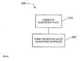
- FIG. 7presents a method of producing an electrode plate for the plasma processing system according to an embodiment of the present invention
- FIG. 8presents a method of producing an electrode plate for the plasma processing system according to another embodiment of the present invention.
- FIG. 9presents a method of producing an electrode plate for the plasma processing system according to another embodiment of the present invention.
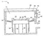
- a plasma processing system 1is depicted in FIG. 1 comprising a plasma processing chamber 10 , an upper assembly 20 , an electrode plate 24 , a substrate holder 30 for supporting a substrate 35 , and a pumping duct 40 coupled to a vacuum pump (not shown) for providing a reduced pressure atmosphere 11 in plasma processing chamber 10 .
- Plasma processing chamber 10can facilitate the formation of a processing plasma in a process space 12 adjacent substrate 35 .
- the plasma processing system 1can be configured to process various substrates (i.e. 200 mm substrates, 300 mm substrates, or larger).
- upper assembly 20can comprise at least one of a cover, a gas injection assembly, and an upper electrode impedance match network.
- the electrode plate 24can be coupled to an RF source, and facilitate an upper electrode for the plasma processing system 1 .
- the upper assembly 20comprises a cover and an electrode plate 24 , wherein the electrode plate 24 is maintained at an electrical potential equivalent to that of the plasma processing chamber 10 .
- the plasma processing chamber 10 , the upper assembly 20 , and the electrode plate 24can be electrically connected to ground potential, and facilitate an upper electrode for the plasma processing system 1 .
- Plasma processing chamber 10can, for example, further comprise a deposition shield 14 for protecting the plasma processing chamber 10 from the processing plasma in the process space 12 , and an optical viewport 16 .
- Optical viewport 16can comprise an optical window 17 coupled to the backside of an optical window deposition shield 18 , and an optical window flange 19 can be configured to couple optical window 17 to the optical window deposition shield 18 .
- Sealing memberssuch as O-rings, can be provided between the optical window flange 19 and the optical window 17 , between the optical window 17 and the optical window deposition shield 18 , and between the optical window deposition shield 18 and the plasma processing chamber 10 .
- Optical window deposition shield 18can extend through an opening 70 within deposition shield 14 .
- Optical viewport 16can, for example, permit monitoring of optical emission from the processing plasma in process space 12 .
- Substrate holder 30can, for example, further comprise a vertical translational device 50 surrounded by a bellows 52 coupled to the substrate holder 30 and the plasma processing chamber 10 , and configured to seal the vertical translational device 50 from the reduced pressure atmosphere 11 in plasma processing chamber 10 .
- a bellows shield 54can, for example, be coupled to the substrate holder 30 and configured to protect the bellows 52 from the processing plasma.
- Substrate holder 10can, for example, further be coupled to at least one of a focus ring 60 , and a shield ring 62 .
- a baffle plate 64can extend about a periphery of the substrate holder 30 .
- Substrate 35can be, for example, transferred into and out of plasma processing chamber 10 through a slot valve (not shown) and chamber feed-through (not shown) via robotic substrate transfer system where it is received by substrate lift pins (not shown) housed within substrate holder 30 and mechanically translated by devices housed therein. Once substrate 35 is received from substrate transfer system, it is lowered to an upper surface of substrate holder 30 .
- Substrate 35can be, for example, affixed to the substrate holder 30 via an electrostatic clamping system.
- substrate holder 30can, for example, further include a cooling system including a re-circulating coolant flow that receives heat from substrate holder 30 and transfers heat to a heat exchanger system (not shown), or when heating, transfers heat from the heat exchanger system.
- gascan, for example, be delivered to the backside of substrate 35 via a backside gas system to improve the gas-gap thermal conductance between substrate 35 and substrate holder 30 .
- Such a systemcan be utilized when temperature control of the substrate is required at elevated or reduced temperatures.
- heating elementssuch as resistive heating elements, or thermoelectric heaters/coolers can be included.
- substrate holder 30can comprise an electrode through which RF power is coupled to the processing plasma in process space 12 .
- substrate holder 30can be electrically biased at a RF voltage via the transmission of RF power from a RF generator (not shown) through an impedance match network (not shown) to substrate holder 30 .
- the RF biascan serve to heat electrons to form and maintain plasma.
- the systemcan operate as a reactive ion etch (RIE) reactor, wherein the chamber and upper gas injection electrode serve as ground surfaces.
- RIEreactive ion etch
- a typical frequency for the RF biascan range from 1 MHz to 100 MHz and is preferably 13.56 MHz.
- RF systems for plasma processingare well known to those skilled in the art.
- the processing plasma formed in process space 12can be formed using a parallel-plate, capacitively coupled plasma (CCP) source, an inductively coupled plasma (ICP) source, any combination thereof, and with and without DC magnet systems.
- the processing plasma in process space 12can be formed using electron cyclotron resonance (ECR).
- ECRelectron cyclotron resonance
- the processing plasma in process space 12is formed from the launching of a Helicon wave.
- the processing plasma in process space 12is formed from a propagating surface wave.
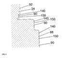
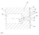
- electrode plate 24comprises a first surface 82 having a coupling surface 82 a for coupling the electrode plate 24 to the upper assembly 20 , a second surface 88 comprising a plasma surface 90 configured to face the processing plasma in the plasma processing chamber 10 and a mating surface 92 for mating the electrode plate 80 with the plasma processing chamber 10 , and a peripheral edge 94 .
- FIG. 4provides an expanded view of the mating surface 92 and the plasma surface 90 in proximity to the peripheral edge 94 of electrode plate 24 .
- the electrode plate 24further includes one or more gas injection orifices 100 coupled to the plenum surface 82 b and the second surface 88 , wherein each gas injection orifice 100 comprises an entrant region 102 for receiving a processing gas and an exit region 104 for coupling the processing gas to the plasma processing chamber 10 , the exit region 104 comprising an injection surface 106 contiguous with the plasma surface 90 .
- the processing gascan, for example, comprise a mixture of gases such as argon, CF 4 and O 2 , or argon, C 4 F 8 and O 2 for oxide etch applications, or other chemistries such as, for example, O 2 /CO/Ar/C 4 F 8 , O 2 /Ar/C 4 F 8 , O 2 /CO/AR/C 5 F 8 , O 2 /CO/Ar/C 4 F 6 , O 2 /Ar/C 4 F 6 , N 2 /H 2 , N 2 /O 2 .
- gasessuch as argon, CF 4 and O 2 , or argon, C 4 F 8 and O 2 for oxide etch applications, or other chemistries such as, for example, O 2 /CO/Ar/C 4 F 8 , O 2 /Ar/C 4 F 8 , O 2 /CO/AR/C 5 F 8 , O 2 /CO/Ar/C 4 F 6 , O 2 /Ar
- the number of gas injection orifices 100 formed within electrode plate 24can range from 1 to 10000. Desirably, the number of gas injection orifices 100 ranges from 50 to 500; and, preferably, the number of gas injection orifices 100 is at least 100. Furthermore, for example, a diameter of the gas injection orifice can range from 0.1 to 20 mm. Desirably, the diameter ranges from 0.5 to 5 mm, and preferably ranges from 0.5 to 2 mm. In addition, for example, a length of a gas injection orifice can range from 1 to 20 mm. Desirably, the length ranges from 2 to 15 mm, and preferably ranges from 3 to 12 mm.
- electrode plate 24comprises a plenum cavity 84 having a plenum surface 82 b that is part of the first surface 82 , configured to receive the processing gas, and configured to distribute the processing gas to the plurality of gas injection orifices 100 .
- electrode plate 24can comprise a first sealing feature 86 coupled to the coupling surface 82 a of the electrode plate 24 and configured to seal the electrode plate 24 with the upper assembly 20 .
- the first sealing featurecan, for example, comprise a dovetail cross-section or rectangular cross-section configured for receiving an O-ring.
- an electrical coupling feature(not shown) can be integrated with the coupling surface 82 a of the electrode plate 24 in order to provide improved electrical coupling between the electrode plate 24 and the upper electrode 20 .
- the electrical coupling featurecan, for example, comprise Spirashield (commercially available from Spira Manufacturing Company), known to those skilled in the art of vacuum processing.
- the electrode plate 24can further include a plurality of fastening receptors 110 for receiving fastening devices (such as bolts) (not shown) in order to attach the electrode plate 24 to the upper assembly 20 .
- the number of fastening receptors 110 formed within electrode plate 24can range from 1 to 100. Desirably, the number of fastening receptors 110 can range from 5 to 20; and, preferably, the number of fastening receptors 110 is at least 8.
- the electrode plate 24can further comprise a diagnostics port 120 , and a second sealing feature 122 coupled to the coupling surface 82 a of the electrode plate 24 and configured to seal the diagnostics port 120 with the upper assembly 20 .
- the diagnostics port 120can include an entrant cavity 124 and an exit through-hole 126 comprising an interior surface 128 contiguous with the plasma surface 90 .
- the second sealing featurecan, for example, comprise a dovetail cross-section or rectangular cross-section configured for receiving an O-ring.
- the diagnostics port 120can be used to couple a diagnostics system (not shown) with the reduced pressure atmosphere 11 of plasma processing chamber 10 .
- the diagnostics systemcan comprise a pressure manometer.
- electrode plate 24can, for example, comprise one or more alignment features 130 in order to provide for proper coupling of the electrode plate 24 to the upper assembly 20 .
- the one or more alignment features 130can, for example, comprise two slots as shown in FIG. 2.
- a plurality of exposed surfaces 140can comprise the plasma surface 90 of the second surface 88 of the electrode plate 24 , the injection surface 106 of the one or more gas injection orifices 100 , and the interior surface 128 of the diagnostics port 120 .
- the exposed surfacescomprise all surfaces on the electrode plate 24 .
- the electrode plate 24further comprises a protective barrier 150 formed on the exposed surfaces 140 of the electrode plate 24 .
- the protective barrier 150can comprise a compound including an oxide of aluminum such as Al 2 O 3 .
- the protective barrier 150comprises a mixture of Al 2 O 3 and Y 2 O 3 .
- the protective barrier 150comprises at least one of a III-column element (column III of periodic table) and a Lanthanon element.
- the III-column elementcomprises at least one of Yttrium, Scandium, and Lanthanum.
- the Lanthanon elementcomprises at least one of Cerium, Dysprosium, and Europium.
- the compound forming protective barrier 150comprises at least one of Yttria (Y 2 O 3 ), Sc 2 O 3 , Sc 2 F 3 , YF 3 , La 2 O 3 , CeO 2 , Eu 2 O 3 , and DyO 3 .
- the protective barrier 150 formed on electrode plate 24comprises a minimum thickness, wherein the minimum thickness can be specified as constant across at least one of the exposed surfaces 140 .
- the minimum thicknesscan be variable across the exposed surfaces 140 .
- the minimum thicknesscan be constant over a first portion of an exposed surface and variable over a second portion of the exposed surface.
- a variable thicknesscan occur on a curved surface, on a corner, or in a hole.
- the minimum thicknesscan ranges from 0.5 micron to 500 micron. Desirably; the minimum thickness can range from 100 micron to 200 micron; and, preferably, the minimum thickness is at least 120 micron.
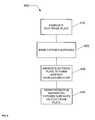
- FIG. 7presents a method of producing the electrode plate in the plasma processing system described in FIG. 1 according to an embodiment of the present invention.
- a flow diagram 300begins in 310 with fabricating the electrode plate (e.g., an electrode plate having the characteristics of the plate described with reference to FIGS. 2 - 6 ).
- Fabricating the electrode platecan comprise at least one of machining, casting, polishing, forging, and grinding.
- each of the elements described abovecan be machined according to specifications set forth on a mechanical drawing, using conventional techniques including a mill, a lathe, etc.
- the techniques for machining a component using, for example, a mill or a latheare well known to those skilled in the art of machining.
- the electrode platecan, for example, be fabricated from aluminum.
- the electrode plateis anodized to form a surface anodization layer.
- the surface anodization layercomprises aluminum oxide (Al 2 O 3 ). Methods of anodizing aluminum components are well known to those skilled in the art of surface anodization.
- the surface anodization layeris removed from the exposed surfaces using standard machining techniques.
- other surfacese.g., the first surface of the electrode plate excluding the plenum cavity, the first sealing feature, and the second sealing feature
- may also be machinede.g., to produce a flat or bare surface that provides at least one of a good mechanical or electrical contact at the machined surface.
- a protective barrier 150(as described above) is formed on the exposed surfaces 140 .
- a protective barriercomprising, for example Yttria, can be formed using (thermal) spray coating techniques that are well known to those skilled in the art of ceramic spray coatings.
- forming the protective barriercan further comprise polishing the thermal spray coating.
- polishing the thermal spray coatingcan comprise the application of sand paper to the sprayed surfaces.
- FIG. 8presents a method of fabricating the electrode plate in the plasma processing system described in FIG. 1 according to another embodiment of the present invention.
- a flow diagram 400begins in 410 with machining the electrode plate (e.g., an electrode plate having the characteristics of the plate described with reference to FIGS. 2 - 6 ).
- Fabricating the electrode platecan comprise at least one of machining, casting, polishing, forging, and grinding.
- each of the elements described abovecan be machined according to specifications set forth on a mechanical drawing, using conventional techniques including a mill, a lathe, etc.
- the techniques for machining a component using, for example, a mill or a latheare well known to those skilled in the art of machining.
- the electrode platecan, for example, be fabricated from aluminum.
- exposed surfaces 140are masked to prevent the formation of a surface anodization layer thereon.
- Techniques for surface masking and unmaskingare well known to those skilled in the art of surface coatings and surface anodization.
- other surfacese.g., the first surface of the electrode plate excluding the plenum cavity, the first sealing feature, and the second sealing feature
- may also be maskede.g., to maintain a flat or bare surface that provides at least one of a good mechanical or electrical contact at the machined surface).
- the electrode plateis anodized to form a surface anodization layer on the remaining unmasked surfaces.
- the surface anodization layercomprise aluminum oxide (Al 2 O 3 ). Methods of anodizing aluminum components are well known to those skilled in the art of surface anodization.
- a protective barrier 150is formed on the exposed surfaces 140 .
- a protective barriercomprising, for example Yttria, can be formed using (thermal) spray coating techniques that are well known to those skilled in the art of ceramic spray coatings.
- forming the protective barriercan further comprise polishing the thermal spray coating.
- polishing the thermal spray coatingcan comprise the application of sand paper to the sprayed surfaces.
- FIG. 9presents a method of producing the electrode plate in the plasma processing system described in FIG. 1 according to another embodiment of the present invention.
- a flow diagram 500begins in 510 with fabricating the electrode plate (e.g., an electrode plate having the characteristics of the plate described with reference to FIGS. 2 - 6 ).
- Fabricating the electrode platecan comprise at least one of machining, casting, polishing, forging, and grinding.
- each of the elements described abovecan be machined according to specifications set forth on a mechanical drawing, using conventional techniques including a mill, a lathe, etc.
- the techniques for machining a component using, for example, a mill or a latheare well known to those skilled in the art of machining.
- the electrode platecan, for example, be fabricated from aluminum.
- a protective barrier 150(as described above) is formed on the exposed surfaces 145 of the electrode plate.
- a protective barriercomprising, for example Yttria, can be formed using (thermal) spray coating techniques that are well known to those skilled in the art of ceramic spray coatings.
- forming the protective barriercan further comprise polishing the thermal spray coating.
- polishing the thermal spray coatingcan comprise the application of sand paper to the sprayed surfaces.
- a mixture of masking and machiningprepares the proper number of surfaces to be protected with a protective barrier 150 .
- the plasma surface of the second surface of the electrode platemay be masked to prevent an anodization layer from being formed thereon, while the injection surface of the exit region in the plurality of gas injection orifices is machined after anodization to present a bare, exposed surface.
Landscapes
- Physics & Mathematics (AREA)
- Engineering & Computer Science (AREA)
- Plasma & Fusion (AREA)
- Chemical & Material Sciences (AREA)
- Analytical Chemistry (AREA)
- Plasma Technology (AREA)
- Drying Of Semiconductors (AREA)
- Sealing Battery Cases Or Jackets (AREA)
- ing And Chemical Polishing (AREA)
Abstract
Description
- This application is related to co-pending U.S. patent application Ser. No. 10/______, entitled “Method and apparatus for an improved upper electrode plate with deposition shield in a plasma processing system”, Attorney docket no. 226272US6YA, filed on even date herewith; co-pending U.S. patent application Ser. No. 10/______, entitled “Method and apparatus for an improved baffle plate in a plasma processing system”, Attorney docket no. 226274US6YA, filed on even date herewith; co-pending U.S. patent application Ser. No. 10/______, entitled “Method and apparatus for an improved baffle plate in a plasma processing system”, Attorney docket no. 228411 US6YA, filed on even date herewith; co-pending U.S. patent application Ser. No. 10/______, entitled “Method and apparatus for an improved deposition shield in a plasma processing system”, Attorney docket no. 226275US6YA, filed on even date herewith; co-pending U.S. patent application Ser. No. 10/______, entitled “Method and apparatus for an improved optical window deposition shield in a plasma processing system”, Attorney docket no. 226276US6YA, filed on even date herewith; and co-pending U.S. patent application Ser. No. 10/______, entitled “Method and apparatus for an improved bellows shield in a plasma processing system”, Attorney docket no. 226277US6YA, filed on even date herewith. The entire contents of all of those applications are herein incorporated by reference in their entirety.[0001]
- The present invention relates to an improved component for a plasma processing system and more particularly to an upper electrode employed in a plasma processing system to introduce a processing gas.[0002]
- The fabrication of integrated circuits (IC) in the semiconductor industry typically employs plasma to create and assist surface chemistry within a plasma reactor necessary to remove material from and deposit material to a substrate. In general, plasma is formed within the plasma reactor under vacuum conditions by heating electrons to energies sufficient to sustain ionizing collisions with a supplied process gas. Moreover, the heated electrons can have energy sufficient to sustain dissociative collisions and, therefore, a specific set of gases under predetermined conditions (e.g., chamber pressure, gas flow rate, etc.) are chosen to produce a population of charged species and chemically reactive species suitable to the particular process being performed within the chamber (e.g., etching processes where materials are removed from the substrate or deposition processes where materials are added to the substrate).[0003]
- Although the formation of a population of charged species (ions, etc.) and chemically reactive species is necessary for performing the function of the plasma processing system (i.e. material etch, material deposition, etc.) at the substrate surface, other component surfaces on the interior of the processing chamber are exposed to the physically and chemically active plasma and, in time, can erode. The erosion of exposed components in the plasma processing system can lead to a gradual degradation of the plasma processing performance and ultimately to complete failure of the system.[0004]
- In order to minimize the damage sustained by exposure to the processing plasma, components of the plasma processing system, known to sustain exposure to the processing plasma, are coated with a protective barrier. For example, components fabricated from aluminum can be anodized to produce a surface layer of aluminum oxide, which is more resistant to the plasma. In another example, a consumable or replaceable component, such as one fabricated from silicon, quartz, alumina, carbon, or silicon carbide, can be inserted within the processing chamber to protect the surfaces of more valuable components that would impose greater costs during frequent replacement. Furthermore, it is desirable to select surface materials that minimize the introduction of unwanted contaminants, impurities, etc. to the processing plasma and possibly to the devices formed on the substrate.[0005]
- In both cases, the inevitable failure of the protective coating, either due to the integrity of the protective barrier or the integrity of the fabrication of the protective barrier, and the consumable nature of the replaceable components demands frequent maintenance of the plasma processing system. This frequent maintenance can produce costs associated with plasma processing down-time and new plasma processing chamber components, which can be excessive.[0006]
- The present invention provides an improved upper electrode for a plasma processing system, wherein the design and fabrication of the upper electrode advantageously addresses the above-identified shortcomings.[0007]
- It is an object of the present invention to provide an electrode plate configured to be coupled to an upper assembly of a plasma processing system comprising a first surface for coupling the electrode plate to the upper assembly, a second surface, opposite the first surface, comprising a plasma surface configured to face a processing plasma in the plasma processing system and a mating surface for mating with the plasma processing system, and a peripheral edge.[0008]
- The electrode plate further comprises one or more gas injection orifices, wherein each gas injection orifice comprises an entrant region for receiving a processing gas and an exit region for coupling the processing gas to the plasma processing system, the exit region comprising an injection surface.[0009]
- The electrode plate further includes a plurality of fastening receptors for receiving fastening devices in order to attach the electrode plate to the upper assembly.[0010]
- The electrode plate further includes a plenum cavity coupled to the first surface, configured to receive the processing gas, and configured to distribute the processing gas to the one or more gas injection orifices.[0011]
- The electrode plate further includes a first sealing feature coupled to the first surface of the electrode plate and configured to seal the electrode plate with the upper assembly.[0012]
- The electrode plate can further comprise a diagnostics port, and a second sealing feature coupled to the first surface of the electrode plate and configured to seal the diagnostics port with the upper assembly. The diagnostics port can include an entrant cavity and an exit through-hole comprising an interior surface.[0013]
- The electrode plate further comprises a protective barrier formed on a plurality of exposed surfaces of the electrode plate facing the processing plasma.[0014]
- It is a further object of the present invention that the plurality of exposed surfaces of the electrode plate can comprise the plasma surface of the second surface of the electrode plate. Additionally, the exposed surfaces can further comprise the injection surface of the exit region in the one or more gas injection orifices, and the interior surface of the exit through-hole in the diagnostics port.[0015]
- The present invention provides a method of producing the electrode plate in the plasma processing system comprising the steps: fabricating the electrode plate; anodizing the electrode plate to form a surface anodization layer on the electrode plate; machining the exposed surfaces on the electrode plate to remove the surface anodization layer; and forming a protective barrier on the exposed surfaces. The present invention may also optionally include machining the first surface of the electrode plate excluding the plenum cavity, the first sealing feature, and the second sealing feature.[0016]
- The present invention provides another method of producing the electrode plate in the plasma processing system comprising the steps: fabricating the electrode plate; masking the exposed surfaces on the electrode plate to prevent formation of a surface anodization layer; anodizing the electrode plate to form the surface anodization layer on the electrode plate; unmasking the exposed surfaces; and forming a protective barrier on the exposed surfaces. The present invention may also optionally include masking other non-exposed surfaces (e.g., the first surface of the electrode plate excluding the plenum cavity, the first sealing feature, and the second sealing feature).[0017]
- The present invention provides another method of producing the electrode plate for the upper electrode in the plasma processing system comprising the steps: fabricating the electrode plate; and forming a protective barrier on the exposed surfaces.[0018]
- The present invention may also include a process of combining machining and masking to prepare the exposed surfaces to receive the protective barrier, and then forming the protective barrier on the exposed surfaces. For example, two of the exposed surfaces can be masked prior to anodizing, and two of the surfaces can be machined after anodizing to create four exposed surfaces on which the protective barrier can be formed.[0019]
- These and other advantages of the invention will become more apparent and more readily appreciated from the following detailed description of the exemplary embodiments of the invention taken in conjunction with the accompanying drawings, where:[0020]
- FIG. 1 shows a simplified block diagram of a plasma processing system comprising an upper electrode including an electrode plate according to an embodiment of the present invention;[0021]
- FIG. 2 shows a plan view of an electrode plate for a plasma processing system according to an embodiment of the present invention;[0022]
- FIG. 3 shows a cross-sectional view of an electrode plate for the plasma processing system according to an embodiment of the present invention;[0023]
- FIG. 4 shows an exploded view of a mating surface and a plasma surface of an electrode plate for the plasma processing system according to an embodiment of the present invention;[0024]
- FIG. 5 shows an exploded view of a gas injection orifice in an electrode plate for the plasma processing system according to an embodiment of the present invention;[0025]
- FIG. 6 shows an exploded view of an exit through-hole of a diagnostics port in an electrode plate for the plasma processing system according to an embodiment of the present invention;[0026]
- FIG. 7 presents a method of producing an electrode plate for the plasma processing system according to an embodiment of the present invention;[0027]
- FIG. 8 presents a method of producing an electrode plate for the plasma processing system according to another embodiment of the present invention; and[0028]
- FIG. 9 presents a method of producing an electrode plate for the plasma processing system according to another embodiment of the present invention.[0029]
- According to an embodiment of the present invention, a[0030]
plasma processing system 1 is depicted in FIG. 1 comprising aplasma processing chamber 10, anupper assembly 20, anelectrode plate 24, asubstrate holder 30 for supporting asubstrate 35, and apumping duct 40 coupled to a vacuum pump (not shown) for providing a reducedpressure atmosphere 11 inplasma processing chamber 10.Plasma processing chamber 10 can facilitate the formation of a processing plasma in aprocess space 12adjacent substrate 35. Theplasma processing system 1 can be configured to process various substrates (i.e. 200 mm substrates, 300 mm substrates, or larger). - In the illustrated embodiment,[0031]
upper assembly 20 can comprise at least one of a cover, a gas injection assembly, and an upper electrode impedance match network. For example, theelectrode plate 24 can be coupled to an RF source, and facilitate an upper electrode for theplasma processing system 1. In another alternate embodiment, theupper assembly 20 comprises a cover and anelectrode plate 24, wherein theelectrode plate 24 is maintained at an electrical potential equivalent to that of theplasma processing chamber 10. For example, theplasma processing chamber 10, theupper assembly 20, and theelectrode plate 24 can be electrically connected to ground potential, and facilitate an upper electrode for theplasma processing system 1. - [0032]
Plasma processing chamber 10 can, for example, further comprise adeposition shield 14 for protecting theplasma processing chamber 10 from the processing plasma in theprocess space 12, and anoptical viewport 16.Optical viewport 16 can comprise anoptical window 17 coupled to the backside of an opticalwindow deposition shield 18, and anoptical window flange 19 can be configured to coupleoptical window 17 to the opticalwindow deposition shield 18. Sealing members, such as O-rings, can be provided between theoptical window flange 19 and theoptical window 17, between theoptical window 17 and the opticalwindow deposition shield 18, and between the opticalwindow deposition shield 18 and theplasma processing chamber 10. Opticalwindow deposition shield 18 can extend through anopening 70 withindeposition shield 14.Optical viewport 16 can, for example, permit monitoring of optical emission from the processing plasma inprocess space 12. - [0033]
Substrate holder 30 can, for example, further comprise a verticaltranslational device 50 surrounded by abellows 52 coupled to thesubstrate holder 30 and theplasma processing chamber 10, and configured to seal the verticaltranslational device 50 from the reducedpressure atmosphere 11 inplasma processing chamber 10. Additionally, abellows shield 54 can, for example, be coupled to thesubstrate holder 30 and configured to protect thebellows 52 from the processing plasma.Substrate holder 10 can, for example, further be coupled to at least one of afocus ring 60, and ashield ring 62. Furthermore, abaffle plate 64 can extend about a periphery of thesubstrate holder 30. - [0034]
Substrate 35 can be, for example, transferred into and out ofplasma processing chamber 10 through a slot valve (not shown) and chamber feed-through (not shown) via robotic substrate transfer system where it is received by substrate lift pins (not shown) housed withinsubstrate holder 30 and mechanically translated by devices housed therein. Oncesubstrate 35 is received from substrate transfer system, it is lowered to an upper surface ofsubstrate holder 30. - [0035]
Substrate 35 can be, for example, affixed to thesubstrate holder 30 via an electrostatic clamping system. Furthermore,substrate holder 30 can, for example, further include a cooling system including a re-circulating coolant flow that receives heat fromsubstrate holder 30 and transfers heat to a heat exchanger system (not shown), or when heating, transfers heat from the heat exchanger system. Moreover, gas can, for example, be delivered to the backside ofsubstrate 35 via a backside gas system to improve the gas-gap thermal conductance betweensubstrate 35 andsubstrate holder 30. Such a system can be utilized when temperature control of the substrate is required at elevated or reduced temperatures. In other embodiments, heating elements, such as resistive heating elements, or thermoelectric heaters/coolers can be included. - In the illustrated embodiment, shown in FIG. 1,[0036]
substrate holder 30 can comprise an electrode through which RF power is coupled to the processing plasma inprocess space 12. For example,substrate holder 30 can be electrically biased at a RF voltage via the transmission of RF power from a RF generator (not shown) through an impedance match network (not shown) tosubstrate holder 30. The RF bias can serve to heat electrons to form and maintain plasma. In this configuration, the system can operate as a reactive ion etch (RIE) reactor, wherein the chamber and upper gas injection electrode serve as ground surfaces. A typical frequency for the RF bias can range from 1 MHz to 100 MHz and is preferably 13.56 MHz. RF systems for plasma processing are well known to those skilled in the art. - Alternately, the processing plasma formed in[0037]
process space 12 can be formed using a parallel-plate, capacitively coupled plasma (CCP) source, an inductively coupled plasma (ICP) source, any combination thereof, and with and without DC magnet systems. Alternately, the processing plasma inprocess space 12 can be formed using electron cyclotron resonance (ECR). In yet another embodiment, the processing plasma inprocess space 12 is formed from the launching of a Helicon wave. In yet another embodiment, the processing plasma inprocess space 12 is formed from a propagating surface wave. - Referring now to an illustrated embodiment of the present invention depicted in FIG. 2 (plan view) and FIG. 3 (cross-sectional view),[0038]
electrode plate 24 comprises afirst surface 82 having acoupling surface 82afor coupling theelectrode plate 24 to theupper assembly 20, asecond surface 88 comprising aplasma surface 90 configured to face the processing plasma in theplasma processing chamber 10 and amating surface 92 for mating theelectrode plate 80 with theplasma processing chamber 10, and aperipheral edge 94. - FIG. 4 provides an expanded view of the[0039]
mating surface 92 and theplasma surface 90 in proximity to theperipheral edge 94 ofelectrode plate 24. - With continuing reference to FIG. 2 and FIG. 3, and as shown in FIG. 5, the[0040]
electrode plate 24 further includes one or moregas injection orifices 100 coupled to theplenum surface 82band thesecond surface 88, wherein eachgas injection orifice 100 comprises anentrant region 102 for receiving a processing gas and anexit region 104 for coupling the processing gas to theplasma processing chamber 10, theexit region 104 comprising aninjection surface 106 contiguous with theplasma surface 90. The processing gas can, for example, comprise a mixture of gases such as argon, CF4and O2, or argon, C4F8and O2for oxide etch applications, or other chemistries such as, for example, O2/CO/Ar/C4F8, O2/Ar/C4F8, O2/CO/AR/C5F8, O2/CO/Ar/C4F6, O2/Ar/C4F6, N2/H2, N2/O2. - For example, the number of[0041]
gas injection orifices 100 formed withinelectrode plate 24 can range from 1 to 10000. Desirably, the number ofgas injection orifices 100 ranges from 50 to 500; and, preferably, the number ofgas injection orifices 100 is at least 100. Furthermore, for example, a diameter of the gas injection orifice can range from 0.1 to 20 mm. Desirably, the diameter ranges from 0.5 to 5 mm, and preferably ranges from 0.5 to 2 mm. In addition, for example, a length of a gas injection orifice can range from 1 to 20 mm. Desirably, the length ranges from 2 to 15 mm, and preferably ranges from 3 to 12 mm. - Additionally, as shown in FIG. 3,[0042]
electrode plate 24 comprises aplenum cavity 84 having aplenum surface 82bthat is part of thefirst surface 82, configured to receive the processing gas, and configured to distribute the processing gas to the plurality of gas injection orifices100. - Additionally,[0043]
electrode plate 24 can comprise afirst sealing feature 86 coupled to thecoupling surface 82aof theelectrode plate 24 and configured to seal theelectrode plate 24 with theupper assembly 20. The first sealing feature can, for example, comprise a dovetail cross-section or rectangular cross-section configured for receiving an O-ring. In an alternate embodiment, an electrical coupling feature (not shown) can be integrated with thecoupling surface 82aof theelectrode plate 24 in order to provide improved electrical coupling between theelectrode plate 24 and theupper electrode 20. The electrical coupling feature can, for example, comprise Spirashield (commercially available from Spira Manufacturing Company), known to those skilled in the art of vacuum processing. - The[0044]
electrode plate 24 can further include a plurality offastening receptors 110 for receiving fastening devices (such as bolts) (not shown) in order to attach theelectrode plate 24 to theupper assembly 20. For example, the number offastening receptors 110 formed withinelectrode plate 24 can range from 1 to 100. Desirably, the number offastening receptors 110 can range from 5 to 20; and, preferably, the number offastening receptors 110 is at least 8. - The[0045]
electrode plate 24 can further comprise adiagnostics port 120, and asecond sealing feature 122 coupled to thecoupling surface 82aof theelectrode plate 24 and configured to seal thediagnostics port 120 with theupper assembly 20. As depicted in FIG. 6, thediagnostics port 120 can include anentrant cavity 124 and an exit through-hole 126 comprising aninterior surface 128 contiguous with theplasma surface 90. Similarly, the second sealing feature can, for example, comprise a dovetail cross-section or rectangular cross-section configured for receiving an O-ring. Thediagnostics port 120 can be used to couple a diagnostics system (not shown) with the reducedpressure atmosphere 11 ofplasma processing chamber 10. For example, the diagnostics system can comprise a pressure manometer. - Additionally,[0046]
electrode plate 24 can, for example, comprise one or more alignment features130 in order to provide for proper coupling of theelectrode plate 24 to theupper assembly 20. The one or more alignment features130 can, for example, comprise two slots as shown in FIG. 2. - As illustrated in FIG. 5 and FIG. 6, a plurality of exposed[0047]
surfaces 140 can comprise theplasma surface 90 of thesecond surface 88 of theelectrode plate 24, theinjection surface 106 of the one or moregas injection orifices 100, and theinterior surface 128 of thediagnostics port 120. Alternately, the exposed surfaces comprise all surfaces on theelectrode plate 24. - Referring now to FIGS. 2 through 6, the[0048]
electrode plate 24 further comprises aprotective barrier 150 formed on the exposedsurfaces 140 of theelectrode plate 24. In an embodiment of the present invention, theprotective barrier 150 can comprise a compound including an oxide of aluminum such as Al2O3. In another embodiment of the present invention, theprotective barrier 150 comprises a mixture of Al2O3and Y2O3. In another embodiment of the present invention, theprotective barrier 150 comprises at least one of a III-column element (column III of periodic table) and a Lanthanon element. In another embodiment of the present invention, the III-column element comprises at least one of Yttrium, Scandium, and Lanthanum. In another embodiment of the present invention, the Lanthanon element comprises at least one of Cerium, Dysprosium, and Europium. In another embodiment of the present invention, the compound formingprotective barrier 150 comprises at least one of Yttria (Y2O3), Sc2O3, Sc2F3, YF3, La2O3, CeO2, Eu2O3, and DyO3. - In an embodiment of the present invention, the[0049]
protective barrier 150 formed onelectrode plate 24 comprises a minimum thickness, wherein the minimum thickness can be specified as constant across at least one of the exposed surfaces140. In another embodiment, the minimum thickness can be variable across the exposed surfaces140. Alternately, the minimum thickness can be constant over a first portion of an exposed surface and variable over a second portion of the exposed surface. For example, a variable thickness can occur on a curved surface, on a corner, or in a hole. For example, the minimum thickness can ranges from 0.5 micron to 500 micron. Desirably; the minimum thickness can range from 100 micron to 200 micron; and, preferably, the minimum thickness is at least 120 micron. - FIG. 7 presents a method of producing the electrode plate in the plasma processing system described in FIG. 1 according to an embodiment of the present invention. A flow diagram[0050]300 begins in310 with fabricating the electrode plate (e.g., an electrode plate having the characteristics of the plate described with reference to FIGS.2-6). Fabricating the electrode plate can comprise at least one of machining, casting, polishing, forging, and grinding. For example, each of the elements described above can be machined according to specifications set forth on a mechanical drawing, using conventional techniques including a mill, a lathe, etc. The techniques for machining a component using, for example, a mill or a lathe, are well known to those skilled in the art of machining. The electrode plate can, for example, be fabricated from aluminum.
- In[0051]320, the electrode plate is anodized to form a surface anodization layer. For example, when fabricating the electrode plate from aluminum, the surface anodization layer comprises aluminum oxide (Al2O3). Methods of anodizing aluminum components are well known to those skilled in the art of surface anodization.
- In[0052]330, the surface anodization layer is removed from the exposed surfaces using standard machining techniques. During the same machining step, or during a separate machining step, other surfaces (e.g., the first surface of the electrode plate excluding the plenum cavity, the first sealing feature, and the second sealing feature) may also be machined (e.g., to produce a flat or bare surface that provides at least one of a good mechanical or electrical contact at the machined surface).
- In[0053]340, a protective barrier150 (as described above) is formed on the exposed surfaces140. A protective barrier comprising, for example Yttria, can be formed using (thermal) spray coating techniques that are well known to those skilled in the art of ceramic spray coatings. In an alternate embodiment, forming the protective barrier can further comprise polishing the thermal spray coating. For example, polishing the thermal spray coating can comprise the application of sand paper to the sprayed surfaces.
- FIG. 8 presents a method of fabricating the electrode plate in the plasma processing system described in FIG. 1 according to another embodiment of the present invention. A flow diagram[0054]400 begins in410 with machining the electrode plate (e.g., an electrode plate having the characteristics of the plate described with reference to FIGS.2-6). Fabricating the electrode plate can comprise at least one of machining, casting, polishing, forging, and grinding. For example, each of the elements described above can be machined according to specifications set forth on a mechanical drawing, using conventional techniques including a mill, a lathe, etc. The techniques for machining a component using, for example, a mill or a lathe, are well known to those skilled in the art of machining. The electrode plate can, for example, be fabricated from aluminum.
- In[0055]420, exposed
surfaces 140 are masked to prevent the formation of a surface anodization layer thereon. Techniques for surface masking and unmasking are well known to those skilled in the art of surface coatings and surface anodization. During the same masking step, or during a separate masking step, other surfaces (e.g., the first surface of the electrode plate excluding the plenum cavity, the first sealing feature, and the second sealing feature) may also be masked (e.g., to maintain a flat or bare surface that provides at least one of a good mechanical or electrical contact at the machined surface). - In[0056]430, the electrode plate is anodized to form a surface anodization layer on the remaining unmasked surfaces. For example, when fabricating the electrode plate with the deposition shield from aluminum, the surface anodization layer comprise aluminum oxide (Al2O3). Methods of anodizing aluminum components are well known to those skilled in the art of surface anodization.
- In[0057]440, the exposed
surfaces 140 are unmasked, and aprotective barrier 150 is formed on the exposed surfaces140. A protective barrier comprising, for example Yttria, can be formed using (thermal) spray coating techniques that are well known to those skilled in the art of ceramic spray coatings. In an alternate embodiment, forming the protective barrier can further comprise polishing the thermal spray coating. For example, polishing the thermal spray coating can comprise the application of sand paper to the sprayed surfaces. - FIG. 9 presents a method of producing the electrode plate in the plasma processing system described in FIG. 1 according to another embodiment of the present invention. A flow diagram[0058]500 begins in510 with fabricating the electrode plate (e.g., an electrode plate having the characteristics of the plate described with reference to FIGS.2-6). Fabricating the electrode plate can comprise at least one of machining, casting, polishing, forging, and grinding. For example, each of the elements described above can be machined according to specifications set forth on a mechanical drawing, using conventional techniques including a mill, a lathe, etc. The techniques for machining a component using, for example, a mill or a lathe, are well known to those skilled in the art of machining. The electrode plate can, for example, be fabricated from aluminum.
- In[0059]520, a protective barrier150 (as described above) is formed on the exposed surfaces145 of the electrode plate. A protective barrier comprising, for example Yttria, can be formed using (thermal) spray coating techniques that are well known to those skilled in the art of ceramic spray coatings. In an alternate embodiment, forming the protective barrier can further comprise polishing the thermal spray coating. For example, polishing the thermal spray coating can comprise the application of sand paper to the sprayed surfaces.
- In an alternate embodiment of the present invention, a mixture of masking and machining prepares the proper number of surfaces to be protected with a[0060]
protective barrier 150. For example, the plasma surface of the second surface of the electrode plate may be masked to prevent an anodization layer from being formed thereon, while the injection surface of the exit region in the plurality of gas injection orifices is machined after anodization to present a bare, exposed surface. - While not necessary in order to form the[0061]
protective barrier 150 on the exposedsurfaces 140, it is also possible to machine other non-exposed surfaces on which an anodization layer has been formed or to mask other non-exposed surfaces prior to performing anodization (e.g., in order to provide a bare surface for an electrical or mechanical connection between parts). Such surfaces may include surfaces of sealing or mating features. - Although only certain exemplary embodiments of this invention have been described in detail above, those skilled in the art will readily appreciate that many modifications are possible in the exemplary embodiments without materially departing from the novel teachings and advantages of this invention. Accordingly, all such modifications are intended to be included within the scope of this invention.[0062]
Claims (79)
1. An upper electrode for a plasma processing system comprising:
an electrode plate comprising a first surface for coupling said electrode plate to an upper assembly, a second surface comprising a plasma surface configured to face a processing space in said plasma processing system and a mating surface for mating said electrode plate with said plasma processing system, a peripheral edge, and one or more gas injection orifices coupled to said first surface and said second surface and configured to couple a processing gas to said processing space; and
a protective barrier coupled to a plurality of exposed surfaces of said electrode plate, said exposed surfaces comprising said plasma surface.
2. The upper electrode as recited inclaim 1 , wherein said electrode plate further comprises a plenum cavity coupled to said first surface, configured to receive said processing gas, and configured to distribute said processing gas to said one or more gas injection orifices.
3. The upper electrode as recited inclaim 1 , wherein said electrode plate further comprises a first sealing feature coupled to said first surface and configured to seal said electrode plate to said upper assembly.
4. The upper electrode as recited inclaim 1 , wherein said electrode plate further comprises a diagnostics port for coupling a diagnostics system to said plasma processing system and a second sealing feature to seal said diagnostics port to said upper assembly.
5. The upper electrode as recited inclaim 1 , wherein said protective barrier comprises a compound containing at least one of a III-column element and a Lanthanon element.
6. The upper electrode as recited inclaim 5 , wherein said III-column element comprises at least one of Yttrium, Scandium, and Lanthanum.
7. The upper electrode as recited inclaim 5 , wherein said Lanthanon element comprises at least one of Cerium, Dysprosium, and Europium.
8. The upper electrode as recited inclaim 1 , wherein said protective barrier comprises at least one of Yttria (Y2O3), Sc2O3, Sc2F3, YF3, La2O3, CeO2, Eu2O3, and DyO3.
9. The upper electrode as recited inclaim 1 , wherein said gas injection orifice comprises an entrant region, and an exit region, wherein said exit region comprises an injection surface.
10. The upper electrode as recited inclaim 1 , wherein said diagnostics port comprises an entrant cavity, and an exit through-hole, wherein said exit through-hole comprises an interior surface.
11. The upper electrode as recited inclaim 9 , wherein said protective barrier is coupled to said injection surface of said gas injection orifice.
12. The upper electrode as recited inclaim 10 , wherein said protective barrier is coupled to said interior surface of said fastening receptor.
13. The upper electrode as recited inclaim 1 , wherein said protective barrier comprises a minimum thickness and said minimum thickness is constant across at least one of said exposed surfaces.
14. The upper electrode as recited inclaim 1 , wherein said protective barrier comprises a variable thickness, said variable thickness ranging from 0.5 microns to 500 microns.
15. The upper electrode as recited inclaim 1 , wherein at least one gas injection orifice has a diameter that is at least 0.1 mm.
16. The upper electrode as recited inclaim 1 , wherein at least one gas injection orifice has a length that is at least 1.0 mm.
17. The upper electrode as recited inclaim 9 , wherein said exposed surfaces further comprise said injection surface of said one or more gas injection orifices.
18. The upper electrode as recited inclaim 10 , wherein said exposed surfaces further comprise said interior surface of said diagnostics port.
19. The upper electrode as recited inclaim 1 , said electrode plate further comprising a metal.
20. The upper electrode as recited inclaim 19 , wherein said metal comprises aluminum.
21. The upper electrode as recited inclaim 1 , wherein said first surface comprises an anodization layer.
22. The upper electrode as recited inclaim 1 , wherein said plenum cavity comprises an anodization layer.
23. The upper electrode as recited inclaim 1 , wherein said mating surface comprises a metallic surface.
24. A method of producing an electrode plate for a plasma processing system, said method comprising the steps:
fabricating said electrode plate, said electrode plate comprising a first surface for coupling said electrode plate to an upper assembly, a second surface comprising a plasma surface configured to face a processing space in said plasma processing system and a mating surface for mating said electrode plate with said plasma processing system, a peripheral edge of said electrode plate, and one or more gas injection orifices coupled to said first surface and said second surface and configured to couple a processing gas to said processing space; and
forming a protective barrier on a plurality of exposed surfaces, said exposed surfaces comprising said plasma surface.
25. The method as recited inclaim 24 , wherein said method further comprises the steps:
anodizing said electrode plate to form a surface anodization layer on said electrode plate; and
machining said exposed surfaces on said electrode plate to remove said surface anodization layer prior to forming said protective barrier on said exposed surfaces.
26. The method as recited inclaim 24 , wherein said method further comprises the steps:
masking said exposed surfaces on said electrode plate;
anodizing said electrode plate to form a surface anodization layer on said electrode plate; and
unmasking said exposed surfaces prior to forming said protective barrier on said exposed surfaces.
27. The method as recited inclaim 24 , wherein said fabricating comprises at least one of machining, casting, polishing, forging, and grinding.
28. The method as recited inclaim 24 , wherein said forming said protective barrier further comprises polishing said protective barrier on at least one of said exposed surfaces.
29. The method as recited inclaim 24 , wherein said electrode plate further comprises a plenum cavity coupled to said first surface, configured to receive said processing gas, and configured to distribute said processing gas to said plurality of gas injection orifices.
30. The method as recited inclaim 24 , wherein said electrode plate further comprises a first sealing feature coupled to said first surface and configured to seal said electrode plate to said upper assembly.
31. The method as recited inclaim 24 , wherein said electrode plate further comprises a diagnostics port for coupling a diagnostics system to said plasma processing system and a second sealing feature to seal said diagnostics port to said upper assembly.
32. The method as recited inclaim 24 , wherein said gas injection orifice comprises an entrant region, and an exit region, wherein said exit region comprises an injection surface.
33. The method as recited inclaim 31 , wherein said diagnostics port comprises an entrant cavity, and an exit through-hole, wherein said exit through-hole comprises an interior surface.
34. The method as recited inclaim 32 , wherein said exposed surfaces further comprise said injection surface of said one or more gas injection orifices.
35. The method as recited inclaim 33 , wherein said exposed surfaces further comprise said interior surface of said diagnostics port.
36. The method as recited inclaim 24 , said electrode plate further comprising a metal.
37. The method as recited inclaim 36 , wherein said metal comprises aluminum.
38. The method as recited inclaim 24 , wherein said protective barrier comprises a compound containing at least one of a III-column element and a Lanthanon element.
39. The method as recited inclaim 38 , wherein said III-column element comprises at least one of Yttrium, Scandium, and Lanthanum.
40. The method as recited inclaim 38 , wherein said Lanthanon element comprises at least one of Cerium, Dysprosium, and Europium.
41. The method as recited inclaim 24 , wherein said protective barrier comprises at least one of Yttria (Y2O3), Sc2O3, Sc2F3, YF3, La2O3, CeO2, Eu2O3, and DyO3.
42. The method as recited inclaim 24 , wherein said protective barrier comprises a minimum thickness and said minimum thickness is constant across at least one of said exposed surfaces.
43. The method as recited inclaim 24 , wherein said protective barrier comprises a varible thickness and said variable thickness ranging from 0.5 microns to 500 microns.
44. The method as recited inclaim 24 , wherein said first surface comprises an anodization layer.
45. The method as recited inclaim 24 , wherein said plenum cavity comprises an anodization layer.
46. The method as recited inclaim 49 , wherein said mating surface comprises a metallic surface.
47. The method as recited inclaim 24 , wherein at least one gas injection orifice has a diameter that is at least 0.1 mm.
48. The method as recited inclaim 24 , wherein at least one gas injection orifice has a length that is at least 1.0 mm.
49. The method as recited inclaim 24 , wherein said fabricating comprises at least one of machining, casting, polishing, forging, and grinding.
50. The method as recited inclaim 24 , wherein said forming a protective barrier further comprises polishing at least one of said exposed surfaces.
51. The method as recited inclaim 24 , wherein said exposed surfaces further comprise all surfaces remaining on said electrode plate.
52. A method of producing an electrode plate capable of being coupled to an upper assembly of a plasma processing system, said method comprising the steps:
fabricating said electrode plate, said electrode plate comprising a first surface for coupling said electrode plate to said upper assembly, a second surface comprising a plasma surface configured to face a processing space in said plasma processing system and a mating surface for mating said electrode plate with said plasma processing system, a peripheral edge of said electrode plate, and one or more gas injection orifices coupled to said first surface and said second surface and configured to couple a processing gas to said processing space;
anodizing said electrode plate to form a surface anodization layer on said electrode plate;
machining exposed surfaces on said electrode plate to remove said surface anodization layer, said exposed surfaces comprising said plasma surface of said second surface of said electrode plate; and
forming a protective barrier on the exposed surfaces.
53. The method as recited inclaim 52 , wherein said electrode plate further comprises a plenum cavity coupled to said first surface, configured to receive said processing gas, and configured to distribute said processing gas to said one or more gas injection orifices.
54. The method as recited inclaim 52 , wherein said electrode plate further comprises a first sealing feature coupled to said first surface and configured to seal said electrode plate to said upper assembly.
55. The method as recited inclaim 52 , wherein said electrode plate further comprises a diagnostics port for coupling a diagnostics system to said plasma processing system and a second sealing feature to seal said diagnostics port to said upper assembly.
56. The method as recited inclaim 52 , wherein said protective barrier comprises a compound containing at least one of a III-column element and a Lanthanon element.
57. The method as recited inclaim 56 , wherein said III-column element comprises at least one of Yttrium, Scandium, and Lanthanum.
58. The method as recited inclaim 56 , wherein said Lanthanon element comprises at least one of Cerium, Dysprosium, and Europium.
59. The method as recited inclaim 56 , wherein said compound comprises Yttria (Y2O3), Sc2O3, Sc2F3, YF3, La2O3, CeO2, Eu2O3, and DyO3.
60. The method as recited inclaim 52 , wherein said fabricating comprises at least one of machining, casting, polishing, forging, and grinding.
61. The method as recited inclaim 52 , wherein said forming a protective barrier further comprises polishing said protective barrier on at least one of said exposed surfaces.
62. The method as recited inclaim 52 , wherein said gas injection orifice comprises an entrant region, and an exit region, wherein said exit region comprises an injection surface.
63. The method as recited inclaim 55 , wherein said diagnostics port comprises an entrant cavity, and an exit through-hole, wherein said exit through-hole comprises an interior surface.
64. The method as recited inclaim 62 , wherein said exposed surfaces further comprise said injection surface of said one or more gas injection orifices.
65. The method as recited inclaim 63 , wherein said exposed surfaces further comprise said interior surface of said diagnostics port.
66. A method of producing an electrode plate capable of being coupled to an upper assembly of a plasma processing system, said method comprising the steps:
fabricating said electrode plate, said electrode plate comprising a first surface for coupling said electrode plate to said upper assembly, a second surface comprising a plasma surface configured to face a processing space in said plasma processing system and a mating surface for mating said electrode plate with said plasma processing system, a peripheral edge of said electrode plate, and one or more gas injection orifices coupled to said first surface and said second surface and configured to couple a processing gas to said processing space;
masking exposed surfaces on said electrode plate to prevent formation of a surface anodization layer, said exposed surfaces comprising said plasma surface of said second surface of said electrode plate;
anodizing said electrode plate to form said surface anodization layer on said electrode plate;
unmasking said exposed surfaces; and
forming a protective barrier on the exposed surfaces.
67. The method as recited inclaim 66 , wherein said electrode plate further comprises a plenum cavity coupled to said first surface, configured to receive said processing gas, and configured to distribute said processing gas to said one or more gas injection orifices.
68. The method as recited inclaim 66 , wherein said electrode plate further comprises a first sealing feature coupled to said first surface and configured to seal said electrode plate to said upper assembly.
69. The method as recited inclaim 66 , wherein said electrode plate further comprises a diagnostics port for coupling a diagnostics system to said plasma processing system and a second sealing feature to seal said diagnostics port to said upper assembly.
70. The method as recited inclaim 66 , wherein said protective barrier comprises a compound containing at least one of a III-column element and a Lanthanon element.
71. The method as recited inclaim 67 , wherein said III-column element comprises at least one of Yttrium, Scandium, and Lanthanum.
72. The method as recited inclaim 67 , wherein said Lanthanon element comprises at least one of Cerium, Dysprosium, and Europium.
73. The method as recited inclaim 67 , wherein said compound comprises Yttria (Y2O3), Sc2O3, Sc2F3, YF3, La2O3, CeO2, Eu2O3, and DyO3.
74. The method as recited inclaim 66 , wherein said fabricating comprises at least one of machining, casting, polishing, forging, and grinding.
75. The method as recited inclaim 66 , wherein said forming a protective barrier further comprises polishing said protective barrier on at least one of said exposed surfaces.
76. The method as recited inclaim 66 , wherein said gas injection orifice comprises an entrant region, and an exit region, wherein said exit region comprises an injection surface.
77. The method as recited inclaim 69 , wherein said diagnostics port comprises an entrant cavity, and an exit through-hole, wherein said exit through-hole comprises an interior surface.
78. The method as recited inclaim 76 , wherein said exposed surfaces further comprise said injection surface of said one or more gas injection orifices.
79. The method as recited inclaim 77 , wherein said exposed surfaces further comprise said interior surface of said diagnostics port.
Priority Applications (7)
| Application Number | Priority Date | Filing Date | Title |
|---|---|---|---|
| US10/259,757US7166200B2 (en) | 2002-09-30 | 2002-09-30 | Method and apparatus for an improved upper electrode plate in a plasma processing system |
| KR1020057005446AKR100753704B1 (en) | 2002-09-30 | 2003-09-29 | Method and apparatus for an improved upper electrode plate in a plasma processing system |
| CNB038232456ACN100555550C (en) | 2002-09-30 | 2003-09-29 | The method and apparatus of the improved electric pole plate in the plasma process system |
| JP2004539373AJP2006501645A (en) | 2002-09-30 | 2003-09-29 | Method and apparatus for improved upper electrode plate in plasma processing system |
| AU2003269393AAU2003269393A1 (en) | 2002-09-30 | 2003-09-29 | Improved upper electrode plate in a plasma processing system and manufacturing method for the electrode |
| PCT/IB2003/004666WO2004030011A2 (en) | 2002-09-30 | 2003-09-29 | Improved upper electrode plate in a plasma processing system and manufacturing method for the electrode |
| US11/567,023US7566368B2 (en) | 2002-09-30 | 2006-12-05 | Method and apparatus for an improved upper electrode plate in a plasma processing system |
Applications Claiming Priority (1)
| Application Number | Priority Date | Filing Date | Title |
|---|---|---|---|
| US10/259,757US7166200B2 (en) | 2002-09-30 | 2002-09-30 | Method and apparatus for an improved upper electrode plate in a plasma processing system |
Related Child Applications (1)
| Application Number | Title | Priority Date | Filing Date |
|---|---|---|---|
| US11/567,023ContinuationUS7566368B2 (en) | 2002-09-30 | 2006-12-05 | Method and apparatus for an improved upper electrode plate in a plasma processing system |
Publications (2)
| Publication Number | Publication Date |
|---|---|
| US20040061447A1true US20040061447A1 (en) | 2004-04-01 |
| US7166200B2 US7166200B2 (en) | 2007-01-23 |
Family
ID=32029554
Family Applications (2)
| Application Number | Title | Priority Date | Filing Date |
|---|---|---|---|
| US10/259,757Expired - LifetimeUS7166200B2 (en) | 2002-09-30 | 2002-09-30 | Method and apparatus for an improved upper electrode plate in a plasma processing system |
| US11/567,023Expired - Fee RelatedUS7566368B2 (en) | 2002-09-30 | 2006-12-05 | Method and apparatus for an improved upper electrode plate in a plasma processing system |
Family Applications After (1)
| Application Number | Title | Priority Date | Filing Date |
|---|---|---|---|
| US11/567,023Expired - Fee RelatedUS7566368B2 (en) | 2002-09-30 | 2006-12-05 | Method and apparatus for an improved upper electrode plate in a plasma processing system |
Country Status (6)
| Country | Link |
|---|---|
| US (2) | US7166200B2 (en) |
| JP (1) | JP2006501645A (en) |
| KR (1) | KR100753704B1 (en) |
| CN (1) | CN100555550C (en) |
| AU (1) | AU2003269393A1 (en) |
| WO (1) | WO2004030011A2 (en) |
Cited By (101)
| Publication number | Priority date | Publication date | Assignee | Title |
|---|---|---|---|---|
| US20030200929A1 (en)* | 1999-12-10 | 2003-10-30 | Hayashi Otsuki | Processing apparatus with a chamber having therein a high-corrosion-resistant sprayed film |
| US20040060661A1 (en)* | 2002-09-30 | 2004-04-01 | Tokyo Electron Limited | Method and apparatus for an improved upper electrode plate with deposition shield in a plasma processing system |
| US20040060656A1 (en)* | 2002-09-30 | 2004-04-01 | Tokyo Electron Limited | Method and apparatus for an improved bellows shield in a plasma processing system |
| US20040060658A1 (en)* | 2002-09-30 | 2004-04-01 | Tokyo Electron Limited | Method and apparatus for an improved baffle plate in a plasma processing system |
| US20040060657A1 (en)* | 2002-09-30 | 2004-04-01 | Tokyo Electron Limited | Method and apparatus for an improved deposition shield in a plasma processing system |
| US20040173155A1 (en)* | 2002-09-30 | 2004-09-09 | Tokyo Electron Limited | Method and apparatus for an improved optical window deposition shield in a plasma processing system |
| US20040216667A1 (en)* | 2002-11-28 | 2004-11-04 | Tokyo Electron Limited | Internal member of a plasma processing vessel |
| US20050150460A1 (en)* | 2003-01-30 | 2005-07-14 | Micron Technology, Inc. | Insitu post atomic layer deposition destruction of active species |
| US20060118045A1 (en)* | 2004-12-08 | 2006-06-08 | Fink Steven T | Method and apparatus for improved baffle plate |
| US20060151114A1 (en)* | 2005-01-11 | 2006-07-13 | Fink Steven T | Plasma processing system and baffle assembly for use in plasma processing system |
| US20060183344A1 (en)* | 2003-03-31 | 2006-08-17 | Tokyo Electron Limited | Barrier layer for a processing element and a method of forming the same |
| US20060225654A1 (en)* | 2005-03-29 | 2006-10-12 | Fink Steven T | Disposable plasma reactor materials and methods |
| US7166166B2 (en) | 2002-09-30 | 2007-01-23 | Tokyo Electron Limited | Method and apparatus for an improved baffle plate in a plasma processing system |
| US7166200B2 (en) | 2002-09-30 | 2007-01-23 | Tokyo Electron Limited | Method and apparatus for an improved upper electrode plate in a plasma processing system |
| US7560376B2 (en) | 2003-03-31 | 2009-07-14 | Tokyo Electron Limited | Method for adjoining adjacent coatings on a processing element |
| US20090206055A1 (en)* | 2008-02-20 | 2009-08-20 | Tokyo Electron Limited | Plasma processing apparatus and method, and baffle plate of the plasma processing apparatus |
| US20140230730A1 (en)* | 2004-04-12 | 2014-08-21 | Applied Materials, Inc. | Gas diffusion shower head design for large area plasma enhanced chemical vapor deposition |
| US20160362782A1 (en)* | 2015-06-15 | 2016-12-15 | Taiwan Semiconductor Manufacturing Co., Ltd. | Gas dispenser and deposition apparatus using the same |
| US20170062184A1 (en)* | 2015-08-27 | 2017-03-02 | Applied Materials, Inc. | Plasma etching systems and methods with secondary plasma injection |
| US9947549B1 (en) | 2016-10-10 | 2018-04-17 | Applied Materials, Inc. | Cobalt-containing material removal |
| US9966240B2 (en) | 2014-10-14 | 2018-05-08 | Applied Materials, Inc. | Systems and methods for internal surface conditioning assessment in plasma processing equipment |
| US9978564B2 (en) | 2012-09-21 | 2018-05-22 | Applied Materials, Inc. | Chemical control features in wafer process equipment |
| US10026621B2 (en) | 2016-11-14 | 2018-07-17 | Applied Materials, Inc. | SiN spacer profile patterning |
| US10032606B2 (en) | 2012-08-02 | 2018-07-24 | Applied Materials, Inc. | Semiconductor processing with DC assisted RF power for improved control |
| US10043674B1 (en) | 2017-08-04 | 2018-08-07 | Applied Materials, Inc. | Germanium etching systems and methods |
| US10043684B1 (en) | 2017-02-06 | 2018-08-07 | Applied Materials, Inc. | Self-limiting atomic thermal etching systems and methods |
| US10049891B1 (en) | 2017-05-31 | 2018-08-14 | Applied Materials, Inc. | Selective in situ cobalt residue removal |
| US10062585B2 (en) | 2016-10-04 | 2018-08-28 | Applied Materials, Inc. | Oxygen compatible plasma source |
| US10062575B2 (en) | 2016-09-09 | 2018-08-28 | Applied Materials, Inc. | Poly directional etch by oxidation |
| US10128086B1 (en) | 2017-10-24 | 2018-11-13 | Applied Materials, Inc. | Silicon pretreatment for nitride removal |
| US10147620B2 (en) | 2015-08-06 | 2018-12-04 | Applied Materials, Inc. | Bolted wafer chuck thermal management systems and methods for wafer processing systems |
| US10163696B2 (en) | 2016-11-11 | 2018-12-25 | Applied Materials, Inc. | Selective cobalt removal for bottom up gapfill |
| US10170336B1 (en) | 2017-08-04 | 2019-01-01 | Applied Materials, Inc. | Methods for anisotropic control of selective silicon removal |
| US10186428B2 (en) | 2016-11-11 | 2019-01-22 | Applied Materials, Inc. | Removal methods for high aspect ratio structures |
| US10224180B2 (en) | 2016-10-04 | 2019-03-05 | Applied Materials, Inc. | Chamber with flow-through source |
| US10224210B2 (en) | 2014-12-09 | 2019-03-05 | Applied Materials, Inc. | Plasma processing system with direct outlet toroidal plasma source |
| US10242908B2 (en) | 2016-11-14 | 2019-03-26 | Applied Materials, Inc. | Airgap formation with damage-free copper |
| US10256079B2 (en) | 2013-02-08 | 2019-04-09 | Applied Materials, Inc. | Semiconductor processing systems having multiple plasma configurations |
| US10256112B1 (en) | 2017-12-08 | 2019-04-09 | Applied Materials, Inc. | Selective tungsten removal |
| US10283321B2 (en) | 2011-01-18 | 2019-05-07 | Applied Materials, Inc. | Semiconductor processing system and methods using capacitively coupled plasma |
| US10283324B1 (en) | 2017-10-24 | 2019-05-07 | Applied Materials, Inc. | Oxygen treatment for nitride etching |
| US10297458B2 (en) | 2017-08-07 | 2019-05-21 | Applied Materials, Inc. | Process window widening using coated parts in plasma etch processes |
| US10319649B2 (en) | 2017-04-11 | 2019-06-11 | Applied Materials, Inc. | Optical emission spectroscopy (OES) for remote plasma monitoring |
| US10319600B1 (en) | 2018-03-12 | 2019-06-11 | Applied Materials, Inc. | Thermal silicon etch |
| US10319739B2 (en) | 2017-02-08 | 2019-06-11 | Applied Materials, Inc. | Accommodating imperfectly aligned memory holes |
| US10319603B2 (en) | 2016-10-07 | 2019-06-11 | Applied Materials, Inc. | Selective SiN lateral recess |
| US10354889B2 (en) | 2017-07-17 | 2019-07-16 | Applied Materials, Inc. | Non-halogen etching of silicon-containing materials |
| US10403507B2 (en) | 2017-02-03 | 2019-09-03 | Applied Materials, Inc. | Shaped etch profile with oxidation |
| US10424485B2 (en) | 2013-03-01 | 2019-09-24 | Applied Materials, Inc. | Enhanced etching processes using remote plasma sources |
| US10424464B2 (en) | 2015-08-07 | 2019-09-24 | Applied Materials, Inc. | Oxide etch selectivity systems and methods |
| US10431429B2 (en) | 2017-02-03 | 2019-10-01 | Applied Materials, Inc. | Systems and methods for radial and azimuthal control of plasma uniformity |
| US10468285B2 (en) | 2015-02-03 | 2019-11-05 | Applied Materials, Inc. | High temperature chuck for plasma processing systems |
| US10465294B2 (en) | 2014-05-28 | 2019-11-05 | Applied Materials, Inc. | Oxide and metal removal |
| US10468267B2 (en) | 2017-05-31 | 2019-11-05 | Applied Materials, Inc. | Water-free etching methods |
| US10468276B2 (en) | 2015-08-06 | 2019-11-05 | Applied Materials, Inc. | Thermal management systems and methods for wafer processing systems |
| US10490406B2 (en) | 2018-04-10 | 2019-11-26 | Appled Materials, Inc. | Systems and methods for material breakthrough |
| US10497573B2 (en) | 2018-03-13 | 2019-12-03 | Applied Materials, Inc. | Selective atomic layer etching of semiconductor materials |
| US10504754B2 (en) | 2016-05-19 | 2019-12-10 | Applied Materials, Inc. | Systems and methods for improved semiconductor etching and component protection |
| US10522371B2 (en) | 2016-05-19 | 2019-12-31 | Applied Materials, Inc. | Systems and methods for improved semiconductor etching and component protection |
| US10541246B2 (en) | 2017-06-26 | 2020-01-21 | Applied Materials, Inc. | 3D flash memory cells which discourage cross-cell electrical tunneling |
| US10541184B2 (en) | 2017-07-11 | 2020-01-21 | Applied Materials, Inc. | Optical emission spectroscopic techniques for monitoring etching |
| US10546729B2 (en) | 2016-10-04 | 2020-01-28 | Applied Materials, Inc. | Dual-channel showerhead with improved profile |
| US10566206B2 (en) | 2016-12-27 | 2020-02-18 | Applied Materials, Inc. | Systems and methods for anisotropic material breakthrough |
| US10573496B2 (en) | 2014-12-09 | 2020-02-25 | Applied Materials, Inc. | Direct outlet toroidal plasma source |
| US10573527B2 (en) | 2018-04-06 | 2020-02-25 | Applied Materials, Inc. | Gas-phase selective etching systems and methods |
| US10593560B2 (en) | 2018-03-01 | 2020-03-17 | Applied Materials, Inc. | Magnetic induction plasma source for semiconductor processes and equipment |
| US10593523B2 (en) | 2014-10-14 | 2020-03-17 | Applied Materials, Inc. | Systems and methods for internal surface conditioning in plasma processing equipment |
| US10615047B2 (en) | 2018-02-28 | 2020-04-07 | Applied Materials, Inc. | Systems and methods to form airgaps |
| US10629473B2 (en) | 2016-09-09 | 2020-04-21 | Applied Materials, Inc. | Footing removal for nitride spacer |
| US10672642B2 (en) | 2018-07-24 | 2020-06-02 | Applied Materials, Inc. | Systems and methods for pedestal configuration |
| US10679870B2 (en) | 2018-02-15 | 2020-06-09 | Applied Materials, Inc. | Semiconductor processing chamber multistage mixing apparatus |
| US10699879B2 (en) | 2018-04-17 | 2020-06-30 | Applied Materials, Inc. | Two piece electrode assembly with gap for plasma control |
| US10727080B2 (en) | 2017-07-07 | 2020-07-28 | Applied Materials, Inc. | Tantalum-containing material removal |
| US10755941B2 (en) | 2018-07-06 | 2020-08-25 | Applied Materials, Inc. | Self-limiting selective etching systems and methods |
| US10854426B2 (en) | 2018-01-08 | 2020-12-01 | Applied Materials, Inc. | Metal recess for semiconductor structures |
| US10872778B2 (en) | 2018-07-06 | 2020-12-22 | Applied Materials, Inc. | Systems and methods utilizing solid-phase etchants |
| US10886137B2 (en) | 2018-04-30 | 2021-01-05 | Applied Materials, Inc. | Selective nitride removal |
| US10892198B2 (en) | 2018-09-14 | 2021-01-12 | Applied Materials, Inc. | Systems and methods for improved performance in semiconductor processing |
| US10903054B2 (en) | 2017-12-19 | 2021-01-26 | Applied Materials, Inc. | Multi-zone gas distribution systems and methods |
| US20210032750A1 (en)* | 2019-07-31 | 2021-02-04 | Taiwan Semiconductor Manufacturing Co., Ltd. | Deposition apparatus and method of forming metal oxide layer using the same |
| US10920320B2 (en) | 2017-06-16 | 2021-02-16 | Applied Materials, Inc. | Plasma health determination in semiconductor substrate processing reactors |
| US10920319B2 (en) | 2019-01-11 | 2021-02-16 | Applied Materials, Inc. | Ceramic showerheads with conductive electrodes |
| US10943834B2 (en) | 2017-03-13 | 2021-03-09 | Applied Materials, Inc. | Replacement contact process |
| US10964512B2 (en) | 2018-02-15 | 2021-03-30 | Applied Materials, Inc. | Semiconductor processing chamber multistage mixing apparatus and methods |
| US11049755B2 (en) | 2018-09-14 | 2021-06-29 | Applied Materials, Inc. | Semiconductor substrate supports with embedded RF shield |
| US11062887B2 (en) | 2018-09-17 | 2021-07-13 | Applied Materials, Inc. | High temperature RF heater pedestals |
| US11121002B2 (en) | 2018-10-24 | 2021-09-14 | Applied Materials, Inc. | Systems and methods for etching metals and metal derivatives |
| US11239061B2 (en) | 2014-11-26 | 2022-02-01 | Applied Materials, Inc. | Methods and systems to enhance process uniformity |
| US11257693B2 (en) | 2015-01-09 | 2022-02-22 | Applied Materials, Inc. | Methods and systems to improve pedestal temperature control |
| US11276559B2 (en) | 2017-05-17 | 2022-03-15 | Applied Materials, Inc. | Semiconductor processing chamber for multiple precursor flow |
| US11276590B2 (en) | 2017-05-17 | 2022-03-15 | Applied Materials, Inc. | Multi-zone semiconductor substrate supports |
| US11328909B2 (en) | 2017-12-22 | 2022-05-10 | Applied Materials, Inc. | Chamber conditioning and removal processes |
| US11384432B2 (en)* | 2015-04-22 | 2022-07-12 | Applied Materials, Inc. | Atomic layer deposition chamber with funnel-shaped gas dispersion channel and gas distribution plate |
| US11417534B2 (en) | 2018-09-21 | 2022-08-16 | Applied Materials, Inc. | Selective material removal |
| US11437242B2 (en) | 2018-11-27 | 2022-09-06 | Applied Materials, Inc. | Selective removal of silicon-containing materials |
| US11594428B2 (en) | 2015-02-03 | 2023-02-28 | Applied Materials, Inc. | Low temperature chuck for plasma processing systems |
| US11682560B2 (en) | 2018-10-11 | 2023-06-20 | Applied Materials, Inc. | Systems and methods for hafnium-containing film removal |
| US11721527B2 (en) | 2019-01-07 | 2023-08-08 | Applied Materials, Inc. | Processing chamber mixing systems |
| US11859284B2 (en)* | 2019-08-23 | 2024-01-02 | Taiwan Semiconductor Manufacturing Company Ltd. | Shower head structure and plasma processing apparatus using the same |
| US12057329B2 (en) | 2016-06-29 | 2024-08-06 | Applied Materials, Inc. | Selective etch using material modification and RF pulsing |
| US12340979B2 (en) | 2017-05-17 | 2025-06-24 | Applied Materials, Inc. | Semiconductor processing chamber for improved precursor flow |
Families Citing this family (26)
| Publication number | Priority date | Publication date | Assignee | Title |
|---|---|---|---|---|
| US20080213496A1 (en)* | 2002-02-14 | 2008-09-04 | Applied Materials, Inc. | Method of coating semiconductor processing apparatus with protective yttrium-containing coatings |
| US20080264564A1 (en) | 2007-04-27 | 2008-10-30 | Applied Materials, Inc. | Method of reducing the erosion rate of semiconductor processing apparatus exposed to halogen-containing plasmas |
| US20050019963A1 (en)* | 2003-07-21 | 2005-01-27 | Texas Instruments Incorporated | Maintaining a reactor chamber of a chemical vapor deposition system |
| TW200526800A (en)* | 2003-12-15 | 2005-08-16 | Applied Materials Inc | Edge flow faceplate for improvement of CVD film properties |
| US7696117B2 (en)* | 2007-04-27 | 2010-04-13 | Applied Materials, Inc. | Method and apparatus which reduce the erosion rate of surfaces exposed to halogen-containing plasmas |
| US10622194B2 (en) | 2007-04-27 | 2020-04-14 | Applied Materials, Inc. | Bulk sintered solid solution ceramic which exhibits fracture toughness and halogen plasma resistance |
| US10242888B2 (en) | 2007-04-27 | 2019-03-26 | Applied Materials, Inc. | Semiconductor processing apparatus with a ceramic-comprising surface which exhibits fracture toughness and halogen plasma resistance |
| US8367227B2 (en)* | 2007-08-02 | 2013-02-05 | Applied Materials, Inc. | Plasma-resistant ceramics with controlled electrical resistivity |
| US7754518B2 (en)* | 2008-02-15 | 2010-07-13 | Applied Materials, Inc. | Millisecond annealing (DSA) edge protection |
| US7987814B2 (en)* | 2008-04-07 | 2011-08-02 | Applied Materials, Inc. | Lower liner with integrated flow equalizer and improved conductance |
| JP5102706B2 (en)* | 2008-06-23 | 2012-12-19 | 東京エレクトロン株式会社 | Baffle plate and substrate processing apparatus |
| US8161906B2 (en)* | 2008-07-07 | 2012-04-24 | Lam Research Corporation | Clamped showerhead electrode assembly |
| US8221582B2 (en) | 2008-07-07 | 2012-07-17 | Lam Research Corporation | Clamped monolithic showerhead electrode |
| US8206506B2 (en) | 2008-07-07 | 2012-06-26 | Lam Research Corporation | Showerhead electrode |
| US8402918B2 (en)* | 2009-04-07 | 2013-03-26 | Lam Research Corporation | Showerhead electrode with centering feature |
| US8272346B2 (en) | 2009-04-10 | 2012-09-25 | Lam Research Corporation | Gasket with positioning feature for clamped monolithic showerhead electrode |
| US8617347B2 (en)* | 2009-08-06 | 2013-12-31 | Applied Materials, Inc. | Vacuum processing chambers incorporating a moveable flow equalizer |
| SG169960A1 (en)* | 2009-09-18 | 2011-04-29 | Lam Res Corp | Clamped monolithic showerhead electrode |
| JP3160877U (en)* | 2009-10-13 | 2010-07-15 | ラム リサーチ コーポレーションLam Research Corporation | End-clamping and machine-fixed inner electrode of showerhead electrode assembly |
| US20110198034A1 (en)* | 2010-02-11 | 2011-08-18 | Jennifer Sun | Gas distribution showerhead with coating material for semiconductor processing |
| JP5198611B2 (en)* | 2010-08-12 | 2013-05-15 | 株式会社東芝 | Gas supply member, plasma processing apparatus, and method for forming yttria-containing film |
| US8573152B2 (en) | 2010-09-03 | 2013-11-05 | Lam Research Corporation | Showerhead electrode |
| JP2012119590A (en)* | 2010-12-02 | 2012-06-21 | Mitsubishi Materials Corp | Electrode plate for plasma processing apparatus |
| TWI480417B (en) | 2012-11-02 | 2015-04-11 | Ind Tech Res Inst | Air showr device having air curtain and apparatus for depositing film using the same |
| JP6339866B2 (en)* | 2014-06-05 | 2018-06-06 | 東京エレクトロン株式会社 | Plasma processing apparatus and cleaning method |
| CN111627790B (en)* | 2019-02-27 | 2024-05-03 | Toto株式会社 | Semiconductor manufacturing device component, semiconductor manufacturing device and display manufacturing device |
Citations (92)
| Publication number | Priority date | Publication date | Assignee | Title |
|---|---|---|---|---|
| US4310390A (en)* | 1977-08-10 | 1982-01-12 | Lockheed Corporation | Protective coating process for aluminum and aluminum alloys |
| US4593007A (en)* | 1984-12-06 | 1986-06-03 | The Perkin-Elmer Corporation | Aluminum and silica clad refractory oxide thermal spray powder |
| US4649858A (en)* | 1984-10-12 | 1987-03-17 | Sumitomo Metal Industries, Ltd. | Repairing apparatus for furnace wall |
| US4842683A (en)* | 1986-12-19 | 1989-06-27 | Applied Materials, Inc. | Magnetic field-enhanced plasma etch reactor |
| US5000113A (en)* | 1986-12-19 | 1991-03-19 | Applied Materials, Inc. | Thermal CVD/PECVD reactor and use for thermal chemical vapor deposition of silicon dioxide and in-situ multi-step planarized process |
| US5423936A (en)* | 1992-10-19 | 1995-06-13 | Hitachi, Ltd. | Plasma etching system |
| US5426310A (en)* | 1989-07-11 | 1995-06-20 | Sony Corporation | Method of heat-treating an oxide optical crystal and a heat treatment apparatus for carrying out the same |
| US5484752A (en)* | 1993-11-12 | 1996-01-16 | Ube Industries, Ltd. | Ceramic composite material |
| US5494713A (en)* | 1994-02-03 | 1996-02-27 | Tokyo Electron Limited | Method for treating surface of aluminum material and plasma treating apparatus |
| US5521790A (en)* | 1994-05-12 | 1996-05-28 | International Business Machines Corporation | Electrostatic chuck having relatively thick and thin areas and means for uniformly cooling said thick and thin areas during chuck anodization |
| US5614055A (en)* | 1993-08-27 | 1997-03-25 | Applied Materials, Inc. | High density plasma CVD and etching reactor |
| US5637237A (en)* | 1994-03-08 | 1997-06-10 | International Business Machines Corporation | Method for hot wall reactive ion etching using a dielectric or metallic liner with temperature control to achieve process stability |
| US5641375A (en)* | 1994-08-15 | 1997-06-24 | Applied Materials, Inc. | Plasma etching reactor with surface protection means against erosion of walls |
| US5651723A (en)* | 1994-04-13 | 1997-07-29 | Viratec Thin Films, Inc. | Method and apparatus for cleaning substrates in preparation for deposition of thin film coatings |
| US5725960A (en)* | 1992-12-28 | 1998-03-10 | Nippon Zeon Co., Ltd. | Molded articles having hard coat layer and method for producing same |
| US5759360A (en)* | 1995-03-13 | 1998-06-02 | Applied Materials, Inc. | Wafer clean sputtering process |
| US5868848A (en)* | 1995-06-07 | 1999-02-09 | Tokyo Electron Limited | Plasma processing apparatus |
| US5879575A (en)* | 1995-11-29 | 1999-03-09 | Applied Materials, Inc. | Self-cleaning plasma processing reactor |
| US5885402A (en)* | 1996-07-17 | 1999-03-23 | Applied Materials | Diagnostic head assembly for plasma chamber |
| US5885356A (en)* | 1994-11-30 | 1999-03-23 | Applied Materials, Inc. | Method of reducing residue accumulation in CVD chamber using ceramic lining |
| US5892278A (en)* | 1996-05-24 | 1999-04-06 | Dai Nippon Printingco., Ltd. | Aluminum and aluminum alloy radiator for semiconductor device and process for producing the same |
| US5891253A (en)* | 1993-05-14 | 1999-04-06 | Applied Materials, Inc. | Corrosion resistant apparatus |
| US5894887A (en)* | 1995-11-30 | 1999-04-20 | Applied Materials, Inc. | Ceramic dome temperature control using heat pipe structure and method |
| US5895586A (en)* | 1994-05-17 | 1999-04-20 | Hitachi, Ltd. | Plasma processing apparatus and plasma processing method in which a part of the processing chamber is formed using a pre-fluorinated material of aluminum |
| US5900064A (en)* | 1997-05-01 | 1999-05-04 | Applied Materials, Inc. | Plasma process chamber |
| US5902763A (en)* | 1995-01-19 | 1999-05-11 | Ube Industries, Inc. | Fused ceramic composite |
| US5911852A (en)* | 1995-06-15 | 1999-06-15 | Sumitomo Metal Industries Limited | Plasma processing apparatus |
| US5919332A (en)* | 1995-06-07 | 1999-07-06 | Tokyo Electron Limited | Plasma processing apparatus |
| US5925228A (en)* | 1997-01-09 | 1999-07-20 | Sandia Corporation | Electrophoretically active sol-gel processes to backfill, seal, and/or densify porous, flawed, and/or cracked coatings on electrically conductive material |
| US6068729A (en)* | 1997-03-03 | 2000-05-30 | Applied Materials, Inc. | Two step process for cleaning a substrate processing chamber |
| US6073449A (en)* | 1996-06-25 | 2000-06-13 | Technova Inc. | Thermoelectric apparatus |
| US6170429B1 (en)* | 1998-09-30 | 2001-01-09 | Lam Research Corporation | Chamber liner for semiconductor process chambers |
| US6176969B1 (en)* | 1998-04-22 | 2001-01-23 | Samsung Electronics Co., Ltd. | Baffle plate of dry etching apparatus for manufacturing semiconductor devices |
| US6182603B1 (en)* | 1998-07-13 | 2001-02-06 | Applied Komatsu Technology, Inc. | Surface-treated shower head for use in a substrate processing chamber |
| US6210486B1 (en)* | 1997-07-16 | 2001-04-03 | Tokyo Electron Limited | CVD film forming method in which a film formation preventing gas is supplied in a direction from a rear surface of an object to be processed |
| US6221202B1 (en)* | 1999-04-01 | 2001-04-24 | International Business Machines Corporation | Efficient plasma containment structure |
| US6246479B1 (en)* | 1998-06-08 | 2001-06-12 | Lj Laboratories, L.L.C. | Integrated spectrometer assembly and methods |
| US20010003271A1 (en)* | 1999-12-10 | 2001-06-14 | Tokyo Electron Limited | Processing apparatus with a chamber having therein a high-corrosion-resistant sprayed film |
| US6265757B1 (en)* | 1999-11-09 | 2001-07-24 | Agere Systems Guardian Corp. | Forming attached features on a semiconductor substrate |
| US6264788B1 (en)* | 1994-04-20 | 2001-07-24 | Tokyo Electron Limited | Plasma treatment method and apparatus |
| US6266133B1 (en)* | 1998-05-06 | 2001-07-24 | Canon Kabushiki Kaisha | Stage device, an exposure apparatus and a device manufacturing method using the same |
| US6335293B1 (en)* | 1998-07-13 | 2002-01-01 | Mattson Technology, Inc. | Systems and methods for two-sided etch of a semiconductor substrate |
| US6364949B1 (en)* | 1999-10-19 | 2002-04-02 | Applied Materials, Inc. | 300 mm CVD chamber design for metal-organic thin film deposition |
| US6368987B1 (en)* | 1997-09-30 | 2002-04-09 | Tokyo Electron Limited | Apparatus and method for preventing the premature mixture of reactant gases in CVD and PECVD reactions |
| US6373573B1 (en)* | 2000-03-13 | 2002-04-16 | Lj Laboratories L.L.C. | Apparatus for measuring optical characteristics of a substrate and pigments applied thereto |
| US6383964B1 (en)* | 1998-11-27 | 2002-05-07 | Kyocera Corporation | Ceramic member resistant to halogen-plasma corrosion |
| US6383333B1 (en)* | 1998-04-28 | 2002-05-07 | Tokai Carbon Company, Ltd. | Protective member for inner surface of chamber and plasma processing apparatus |
| US6394026B1 (en)* | 1998-03-31 | 2002-05-28 | Lam Research Corporation | Low contamination high density plasma etch chambers and methods for making the same |
| US20020076508A1 (en)* | 2000-12-15 | 2002-06-20 | Chiang Tony P. | Varying conductance out of a process region to control gas flux in an ALD reactor |
| US6413578B1 (en)* | 2000-10-12 | 2002-07-02 | General Electric Company | Method for repairing a thermal barrier coating and repaired coating formed thereby |
| US20020086545A1 (en)* | 2000-12-29 | 2002-07-04 | O'donnell Robert J. | Corrosion resistant component of semiconductor processing equipment and method of manufacture thereof |
| US20020086118A1 (en)* | 2000-12-29 | 2002-07-04 | Chang Christopher C. | Low contamination plasma chamber components and methods for making the same |
| US20020086553A1 (en)* | 2000-12-29 | 2002-07-04 | O'donnell Robert J. | Fullerene coated component of semiconductor processing equipment and method of manufacturing thereof |
| US20020086501A1 (en)* | 2000-12-29 | 2002-07-04 | O'donnell Robert J. | Diamond coatings on reactor wall and method of manufacturing thereof |
| US20020090464A1 (en)* | 2000-11-28 | 2002-07-11 | Mingwei Jiang | Sputter chamber shield |
| US20030010446A1 (en)* | 1999-04-16 | 2003-01-16 | Morio Kajiyama | Method of manufacturing a processing apparatus |
| US6514377B1 (en)* | 1999-09-08 | 2003-02-04 | Tokyo Electron Limited | Apparatus for and method of processing an object to be processed |
| US6519037B2 (en)* | 1999-12-23 | 2003-02-11 | Lj Laboratories, Llc | Spectrometer having optical unit including a randomized fiber optic implement |
| US20030029563A1 (en)* | 2001-08-10 | 2003-02-13 | Applied Materials, Inc. | Corrosion resistant coating for semiconductor processing chamber |
| US6527911B1 (en)* | 2001-06-29 | 2003-03-04 | Lam Research Corporation | Configurable plasma volume etch chamber |
| US6533910B2 (en)* | 2000-12-29 | 2003-03-18 | Lam Research Corporation | Carbonitride coated component of semiconductor processing equipment and method of manufacturing thereof |
| US6554906B1 (en)* | 2000-01-20 | 2003-04-29 | Sumitomo Electric Industries, Ltd. | Wafer holder for semiconductor manufacturing apparatus and semiconductor manufacturing apparatus using the same |
| US20030084848A1 (en)* | 2001-06-22 | 2003-05-08 | Tokyo Electron Limited | Gas temperature control for a plasma process |
| US6562186B1 (en)* | 1998-08-31 | 2003-05-13 | Tokyo Electron Limited | Apparatus for plasma processing |
| US6570654B2 (en)* | 1997-01-02 | 2003-05-27 | Lj Laboratories Llc | Apparatus and method for measuring optical characteristics of an object |
| US20030113479A1 (en)* | 2001-08-23 | 2003-06-19 | Konica Corporation | Atmospheric pressure plasma treatmet apparatus and atmospheric pressure plasma treatment method |
| US6590660B2 (en)* | 1999-12-23 | 2003-07-08 | Lj Laboratories Llc | Apparatus and method for measuring optical characteristics of an object |
| US6695929B2 (en)* | 2001-02-07 | 2004-02-24 | Sumitomo Special Co., Ltd. | Method of making material alloy for iron-based rare earth magnet |
| US20040035364A1 (en)* | 2000-11-13 | 2004-02-26 | Riki Tomoyoshi | Plasma processing apparatus and method for asssembling the plasma processing apparatus |
| US20040050495A1 (en)* | 2002-09-13 | 2004-03-18 | Masahiro Sumiya | Plasma processing apparatus and plasma processing method |
| US20040060657A1 (en)* | 2002-09-30 | 2004-04-01 | Tokyo Electron Limited | Method and apparatus for an improved deposition shield in a plasma processing system |
| US20040060516A1 (en)* | 2002-09-30 | 2004-04-01 | Tokyo Electron Limited | Method and apparatus for an improved optical window deposition shield in a plasma processing system |
| US20040060661A1 (en)* | 2002-09-30 | 2004-04-01 | Tokyo Electron Limited | Method and apparatus for an improved upper electrode plate with deposition shield in a plasma processing system |
| US20040060656A1 (en)* | 2002-09-30 | 2004-04-01 | Tokyo Electron Limited | Method and apparatus for an improved bellows shield in a plasma processing system |
| US20040060658A1 (en)* | 2002-09-30 | 2004-04-01 | Tokyo Electron Limited | Method and apparatus for an improved baffle plate in a plasma processing system |
| US20040060779A1 (en)* | 2002-10-01 | 2004-04-01 | Charles Kreger | Distance compensating shim for clutch/brake and method of determining same |
| US20040063333A1 (en)* | 2002-09-30 | 2004-04-01 | Tokyo Electron Limited | Method and apparatus for an improved baffle plate in a plasma processing system |
| US20040072426A1 (en)* | 2002-08-02 | 2004-04-15 | Soon-Jong Jung | Process chamber for manufacturing a smiconductor device |
| US6726801B2 (en)* | 2001-07-24 | 2004-04-27 | Samsung Electronics Co., Ltd. | Dry etching apparatus for manufacturing semiconductor devices |
| US20040081746A1 (en)* | 2000-12-12 | 2004-04-29 | Kosuke Imafuku | Method for regenerating container for plasma treatment, member inside container for plasma treatment, method for preparing member inside container for plasma treatment, and apparatus for plasma treatment |
| US20040083970A1 (en)* | 2000-10-02 | 2004-05-06 | Kosuke Imafuku | Vacuum processing device |
| US6733620B1 (en)* | 1998-03-06 | 2004-05-11 | Tokyo Electron Limited | Process apparatus |
| US6738862B1 (en)* | 1998-08-07 | 2004-05-18 | Cisco Technology, Inc. | Block mask ternary CAM |
| US20040125359A1 (en)* | 2002-12-31 | 2004-07-01 | Tokyo Electron Limited | Monitoring material buildup on system components by optical emission |
| US6852433B2 (en)* | 2002-07-19 | 2005-02-08 | Shin-Etsu Chemical Co., Ltd. | Rare-earth oxide thermal spray coated articles and powders for thermal spraying |
| US6863594B2 (en)* | 2000-03-15 | 2005-03-08 | Paul-Eric Preising | Method and device for cleaning high-voltage carrying installation component parts |
| US6875477B2 (en)* | 2003-02-04 | 2005-04-05 | Hitachi High-Technologies Corporation | Method for coating internal surface of plasma processing chamber |
| US6884516B2 (en)* | 1999-12-10 | 2005-04-26 | Tocalo Co., Ltd. | Internal member for plasma-treating vessel and method of producing the same |
| US6894769B2 (en)* | 2002-12-31 | 2005-05-17 | Tokyo Electron Limited | Monitoring erosion of system components by optical emission |
| US20050103275A1 (en)* | 2003-02-07 | 2005-05-19 | Tokyo Electron Limited | Plasma processing apparatus, ring member and plasma processing method |
| US6896785B2 (en)* | 2002-03-27 | 2005-05-24 | Isle Coat Limited | Process and device for forming ceramic coatings on metals and alloys, and coatings produced by this process |
| US20060134919A1 (en)* | 2003-03-17 | 2006-06-22 | Tokyo Electron Limited | Processing system and method for treating a substrate |
Family Cites Families (127)
| Publication number | Priority date | Publication date | Assignee | Title |
|---|---|---|---|---|
| JPS6057396B2 (en) | 1976-09-29 | 1985-12-14 | 大成化工株式会社 | Manufacturing method of double tube |
| JPS63450Y2 (en) | 1980-03-26 | 1988-01-07 | ||
| US4357387A (en) | 1981-08-20 | 1982-11-02 | Subtex, Inc. | Flame resistant insulating fabric compositions prepared by plasma spraying |
| JPS5857491A (en) | 1981-09-30 | 1983-04-05 | Sony Corp | Preparation of green fluorescent material |
| JPS59159510A (en) | 1983-03-01 | 1984-09-10 | Canon Inc | magneto-optical recording medium |
| JPS59186325A (en)* | 1983-04-01 | 1984-10-23 | コンパニ−・アンデユストリエル・デ・テレコミユニカシオン・セイテ−アルカテル | dry etching equipment |
| JPS60136505U (en) | 1984-02-21 | 1985-09-10 | 三菱電機株式会社 | Reflection free terminator |
| JPS60142822U (en) | 1984-03-01 | 1985-09-21 | パイオニア株式会社 | optical disc player |
| JPS61207566A (en) | 1985-03-12 | 1986-09-13 | Showa Denko Kk | Ceramic thermal spray coating formation method |
| US4612077A (en)* | 1985-07-29 | 1986-09-16 | The Perkin-Elmer Corporation | Electrode for plasma etching system |
| JPS6267161U (en) | 1985-10-15 | 1987-04-25 | ||
| JPH0611346Y2 (en) | 1986-06-30 | 1994-03-23 | 不二サッシ株式会社 | Opening / closing device for sliding doors inside / outside windows |
| US4985102A (en) | 1986-07-17 | 1991-01-15 | Du Pont Canada Inc. | Method of making fiber reinforced polyamide sheets |
| US4877757A (en) | 1987-07-16 | 1989-10-31 | Texas Instruments Incorporated | Method of sequential cleaning and passivating a GaAs substrate using remote oxygen plasma |
| JPH0423551Y2 (en) | 1987-09-04 | 1992-06-02 | ||
| NO163412B (en) | 1988-01-25 | 1990-02-12 | Elkem Technology | The plasma torch. |
| JPH01120328U (en) | 1988-02-08 | 1989-08-15 | ||
| JPH0730468B2 (en) | 1988-06-09 | 1995-04-05 | 日電アネルバ株式会社 | Dry etching equipment |
| JPH0657396B2 (en) | 1989-02-17 | 1994-08-03 | レンゴー株式会社 | Rotary shear control method and device |
| JPH02267967A (en) | 1989-04-07 | 1990-11-01 | Fuji Electric Co Ltd | Manufacture of semiconductor element |
| US5334462A (en) | 1989-09-08 | 1994-08-02 | United Technologies Corporation | Ceramic material and insulating coating made thereof |
| JPH03115535A (en) | 1989-09-28 | 1991-05-16 | Nippon Mining Co Ltd | Oxygen reduction method for rare earth metals |
| US5556501A (en) | 1989-10-03 | 1996-09-17 | Applied Materials, Inc. | Silicon scavenger in an inductively coupled RF plasma reactor |
| US5126102A (en)* | 1990-03-15 | 1992-06-30 | Kabushiki Kaisha Toshiba | Fabricating method of composite material |
| DE4109979C2 (en)* | 1990-03-28 | 2000-03-30 | Nisshin Flour Milling Co | Process for the production of coated particles from inorganic or metallic materials |
| US5180467A (en)* | 1990-08-08 | 1993-01-19 | Vlsi Technology, Inc. | Etching system having simplified diffuser element removal |
| US5074456A (en)* | 1990-09-18 | 1991-12-24 | Lam Research Corporation | Composite electrode for plasma processes |
| JPH04238882A (en) | 1991-01-10 | 1992-08-26 | Denki Kagaku Kogyo Kk | High-temperature insulated article |
| DE4103994A1 (en) | 1991-02-11 | 1992-08-13 | Inst Elektroswarki Patona | PROTECTIVE COVER OF THE METAL-CERAMIC TYPE FOR ITEMS OF HEAT-RESISTANT ALLOYS |
| EP0508731B1 (en)* | 1991-04-09 | 1996-09-18 | The Tokyo Electric Power Co., Inc. | Use of an oxide coating to enhance the resistance to oxidation and corrosion of a silicon nitride based gas turbine blade |
| JPH05117064A (en) | 1991-04-09 | 1993-05-14 | Tokyo Electric Power Co Inc:The | Blade for gas turbine and its production |
| JPH05121360A (en) | 1991-04-22 | 1993-05-18 | Tokyo Electron Yamanashi Kk | Semiconductor processor |
| JPH05198532A (en) | 1992-01-22 | 1993-08-06 | Hitachi Chem Co Ltd | Electrode plate for plasma etching device |
| JPH05238855A (en) | 1992-02-28 | 1993-09-17 | Tokyo Electric Power Co Inc:The | Production of ceramic coating member |
| JPH05238859A (en) | 1992-02-28 | 1993-09-17 | Tokyo Electric Power Co Inc:The | Coated member of ceramic |
| AU4302893A (en) | 1992-06-01 | 1993-12-30 | Ice Blast International Ltd. | Particle blasting utilizing crystalline ice |
| EP0573057A1 (en) | 1992-06-05 | 1993-12-08 | Applied Materials, Inc. | Integrated circuit structure processing apparatus with chemically corrosion-resistant Al2O3 protective coating on surface of quartz window exposed to corrosive chemicals |
| JPH06136505A (en) | 1992-10-26 | 1994-05-17 | Sumitomo Metal Ind Ltd | Sprayed coating structure |
| JPH06142822A (en) | 1992-11-09 | 1994-05-24 | Kawasaki Steel Corp | Method for manufacturing high melting point active metal casting mold |
| JPH06196548A (en) | 1992-12-24 | 1994-07-15 | Sumitomo Metal Ind Ltd | Electrostatic chuck |
| US5366585A (en) | 1993-01-28 | 1994-11-22 | Applied Materials, Inc. | Method and apparatus for protection of conductive surfaces in a plasma processing reactor |
| JPH06256926A (en) | 1993-03-08 | 1994-09-13 | Mitsubishi Heavy Ind Ltd | Coating film for heat shielding |
| US5362335A (en) | 1993-03-25 | 1994-11-08 | General Motors Corporation | Rare earth coating process for aluminum alloys |
| KR100324792B1 (en) | 1993-03-31 | 2002-06-20 | 히가시 데쓰로 | Plasma processing apparatus |
| JP3236398B2 (en) | 1993-04-02 | 2001-12-10 | 株式会社フジクラ | Thermal spray equipment |
| US5551190A (en) | 1993-05-19 | 1996-09-03 | Ohi Seisakusho Co., Ltd. | Slide door driving system |
| JPH0758013A (en) | 1993-08-10 | 1995-03-03 | Hitachi Ltd | Semiconductor film forming equipment |
| JPH07126827A (en) | 1993-10-28 | 1995-05-16 | Nippon Alum Co Ltd | Composite film of metallic surface and its formation |
| JP3228644B2 (en) | 1993-11-05 | 2001-11-12 | 東京エレクトロン株式会社 | Material for vacuum processing apparatus and method for producing the same |
| JPH07226378A (en) | 1994-02-10 | 1995-08-22 | Sony Corp | Film forming method and plasma device using for this method |
| JP3061346B2 (en) | 1994-03-07 | 2000-07-10 | 東京エレクトロン株式会社 | Processing equipment |
| US5680013A (en) | 1994-03-15 | 1997-10-21 | Applied Materials, Inc. | Ceramic protection for heated metal surfaces of plasma processing chamber exposed to chemically aggressive gaseous environment therein and method of protecting such heated metal surfaces |
| JPH0841309A (en) | 1994-07-28 | 1996-02-13 | Hoechst Japan Ltd | Polybenzimidazole-based resin articles for dry etching equipment |
| DE9421671U1 (en) | 1994-08-26 | 1996-07-11 | Siemens AG, 80333 München | Discharge chamber for a plasma etching system in semiconductor production |
| JP3473121B2 (en) | 1994-09-14 | 2003-12-02 | ソニー株式会社 | Plasma CVD apparatus and plasma CVD method |
| US5891350A (en) | 1994-12-15 | 1999-04-06 | Applied Materials, Inc. | Adjusting DC bias voltage in plasma chambers |
| JPH08227874A (en)* | 1995-02-21 | 1996-09-03 | Mitsubishi Electric Corp | Vacuum processing apparatus and vacuum processing method |
| JP3420377B2 (en) | 1995-03-29 | 2003-06-23 | 京セラ株式会社 | Method for producing yttrium-aluminum-garnet sintered body |
| US6296740B1 (en) | 1995-04-24 | 2001-10-02 | Si Diamond Technology, Inc. | Pretreatment process for a surface texturing process |
| US5534356A (en)* | 1995-04-26 | 1996-07-09 | Olin Corporation | Anodized aluminum substrate having increased breakdown voltage |
| JPH08339895A (en) | 1995-06-12 | 1996-12-24 | Tokyo Electron Ltd | Plasma processing device |
| DE19529627C1 (en) | 1995-08-11 | 1997-01-16 | Siemens Ag | Thermally conductive, electrically insulating connection and method for its production |
| JP2971369B2 (en) | 1995-08-31 | 1999-11-02 | トーカロ株式会社 | Electrostatic chuck member and method of manufacturing the same |
| US5985102A (en) | 1996-01-29 | 1999-11-16 | Micron Technology, Inc. | Kit for electrically isolating collimator of PVD chamber, chamber so modified, and method of using |
| JP4226669B2 (en) | 1996-02-05 | 2009-02-18 | 株式会社東芝 | Heat resistant material |
| US5955182A (en) | 1996-02-05 | 1999-09-21 | Kabushiki Kaisha Toshiba | Heat resisting member and its production method |
| JP3035209B2 (en) | 1996-02-27 | 2000-04-24 | 三菱重工業株式会社 | Corrosion resistant material and method for producing the same |
| JPH09235662A (en) | 1996-02-28 | 1997-09-09 | Nittetsu Hard Kk | Formation of thermally sprayed coating |
| CN1074689C (en) | 1996-04-04 | 2001-11-14 | E·O·帕通电子焊接研究院电子束工艺国际中心 | Method of producing on substrate of protective coatings with chemical composition and structure gradient across thickness and with top ceramic layer |
| US6108189A (en) | 1996-04-26 | 2000-08-22 | Applied Materials, Inc. | Electrostatic chuck having improved gas conduits |
| CA2205817C (en) | 1996-05-24 | 2004-04-06 | Sekisui Chemical Co., Ltd. | Treatment method in glow-discharge plasma and apparatus thereof |
| JP3050124B2 (en) | 1996-05-27 | 2000-06-12 | 住友金属工業株式会社 | Plasma processing equipment |
| US5820723A (en)* | 1996-06-05 | 1998-10-13 | Lam Research Corporation | Universal vacuum chamber including equipment modules such as a plasma generating source, vacuum pumping arrangement and/or cantilevered substrate support |
| US5952060A (en) | 1996-06-14 | 1999-09-14 | Applied Materials, Inc. | Use of carbon-based films in extending the lifetime of substrate processing system components |
| JPH104083A (en) | 1996-06-17 | 1998-01-06 | Kyocera Corp | Corrosion resistant materials for semiconductor manufacturing |
| US5904778A (en)* | 1996-07-26 | 1999-05-18 | Applied Materials, Inc. | Silicon carbide composite article particularly useful for plasma reactors |
| JP3261044B2 (en) | 1996-07-31 | 2002-02-25 | 京セラ株式会社 | Components for plasma processing equipment |
| JP3619330B2 (en) | 1996-07-31 | 2005-02-09 | 京セラ株式会社 | Components for plasma process equipment |
| US5882411A (en)* | 1996-10-21 | 1999-03-16 | Applied Materials, Inc. | Faceplate thermal choke in a CVD plasma reactor |
| JPH10130884A (en) | 1996-10-25 | 1998-05-19 | Nagayama Kogyosho:Kk | Treatment of heat resistant anodically oxidized coating |
| US6120640A (en) | 1996-12-19 | 2000-09-19 | Applied Materials, Inc. | Boron carbide parts and coatings in a plasma reactor |
| JPH10214819A (en) | 1997-01-28 | 1998-08-11 | Sumitomo Metal Ind Ltd | Electrode plate for plasma etching |
| US5800621A (en) | 1997-02-10 | 1998-09-01 | Applied Materials, Inc. | Plasma source for HDP-CVD chamber |
| JPH10226869A (en) | 1997-02-17 | 1998-08-25 | Mitsui Eng & Shipbuild Co Ltd | Plasma spraying method |
| JPH111757A (en) | 1997-04-14 | 1999-01-06 | Toshiba Ceramics Co Ltd | Jig for burning in nonoxidizing atmosphere |
| US5851343A (en) | 1997-05-16 | 1998-12-22 | Taiwan Semiconductor Manufacturing Company, Ltd. | Protective shield around the inner edge of endpoint window in a plasma etching chamber |
| US5994662A (en) | 1997-05-29 | 1999-11-30 | Applied Materials, Inc. | Unique baffle to deflect remote plasma clean gases |
| US6143646A (en) | 1997-06-03 | 2000-11-07 | Motorola Inc. | Dual in-laid integrated circuit structure with selectively positioned low-K dielectric isolation and method of formation |
| JP3707229B2 (en) | 1997-06-27 | 2005-10-19 | コニカミノルタビジネステクノロジーズ株式会社 | Electrophotographic photosensitive member and electrophotographic image forming apparatus using the same |
| JP3362113B2 (en) | 1997-07-15 | 2003-01-07 | 日本碍子株式会社 | Corrosion-resistant member, wafer mounting member, and method of manufacturing corrosion-resistant member |
| KR19990008937U (en) | 1997-08-13 | 1999-03-05 | 이문세 | Soundproof wall assembly |
| US6106625A (en) | 1997-12-02 | 2000-08-22 | Applied Materials, Inc. | Reactor useful for chemical vapor deposition of titanium nitride |
| US6079356A (en)* | 1997-12-02 | 2000-06-27 | Applied Materials, Inc. | Reactor optimized for chemical vapor deposition of titanium |
| KR100258984B1 (en) | 1997-12-24 | 2000-08-01 | 윤종용 | Dry etching apparatus |
| JPH11207161A (en) | 1998-01-22 | 1999-08-03 | Konica Corp | Device for dissolving solid treating agent |
| JP3350433B2 (en) | 1998-02-16 | 2002-11-25 | シャープ株式会社 | Plasma processing equipment |
| KR100602072B1 (en) | 1998-03-31 | 2006-07-14 | 램 리서치 코포레이션 | Pollution Control Method and Plasma Processing Chamber |
| JP3555442B2 (en) | 1998-04-24 | 2004-08-18 | 住友金属工業株式会社 | Alumina ceramic material excellent in plasma corrosion resistance and method for producing the same |
| US6123791A (en) | 1998-07-29 | 2000-09-26 | Applied Materials, Inc. | Ceramic composition for an apparatus and method for processing a substrate |
| JP3030287B1 (en) | 1998-10-09 | 2000-04-10 | 株式会社協同インターナショナル | Method for cleaning film forming apparatus, method for cleaning sputtering target, and cleaning apparatus used for these |
| JP2000124197A (en) | 1998-10-16 | 2000-04-28 | Hitachi Ltd | Plasma processing equipment |
| US6123804A (en) | 1999-02-22 | 2000-09-26 | Applied Materials, Inc. | Sectional clamp ring |
| JP4055880B2 (en)* | 1999-06-02 | 2008-03-05 | 東京エレクトロン株式会社 | Plasma processing apparatus, plasma processing monitoring window member, and electrode plate for plasma processing apparatus |
| US6444083B1 (en) | 1999-06-30 | 2002-09-03 | Lam Research Corporation | Corrosion resistant component of semiconductor processing equipment and method of manufacturing thereof |
| JP2001023959A (en) | 1999-07-05 | 2001-01-26 | Mitsubishi Electric Corp | Plasma processing equipment |
| JP2001031484A (en) | 1999-07-22 | 2001-02-06 | Nihon Ceratec Co Ltd | Corrosion-resistant composite member |
| US6387817B1 (en)* | 1999-09-07 | 2002-05-14 | Agere Systems Guardian Corp. | Plasma confinement shield |
| US6296716B1 (en) | 1999-10-01 | 2001-10-02 | Saint-Gobain Ceramics And Plastics, Inc. | Process for cleaning ceramic articles |
| JP2001152307A (en) | 1999-11-29 | 2001-06-05 | Nippon Steel Hardfacing Co Ltd | Method of forming corrosion resisting combined coating standing long use, and member having the composite coating |
| JP3798597B2 (en)* | 1999-11-30 | 2006-07-19 | 富士通株式会社 | Semiconductor device |
| JP4272786B2 (en) | 2000-01-21 | 2009-06-03 | トーカロ株式会社 | Electrostatic chuck member and manufacturing method thereof |
| JP3643540B2 (en)* | 2000-02-21 | 2005-04-27 | 株式会社日立製作所 | Plasma processing equipment |
| TW503449B (en) | 2000-04-18 | 2002-09-21 | Ngk Insulators Ltd | Halogen gas plasma-resistive members and method for producing the same, laminates, and corrosion-resistant members |
| JP4422295B2 (en) | 2000-05-17 | 2010-02-24 | キヤノンアネルバ株式会社 | CVD equipment |
| EP1167565B1 (en)* | 2000-06-29 | 2007-03-07 | Shin-Etsu Chemical Co., Ltd. | Method for thermal spray coating and rare earth oxide powder used therefor |
| CN100386467C (en) | 2000-12-12 | 2008-05-07 | 东京毅力科创株式会社 | Method for regenerating plasma processing container, internal component of plasma processing container, method for manufacturing internal component of plasma processing container, and plasma processing apparatus |
| US6613442B2 (en)* | 2000-12-29 | 2003-09-02 | Lam Research Corporation | Boron nitride/yttria composite components of semiconductor processing equipment and method of manufacturing thereof |
| US6830622B2 (en) | 2001-03-30 | 2004-12-14 | Lam Research Corporation | Cerium oxide containing ceramic components and coatings in semiconductor processing equipment and methods of manufacture thereof |
| TW541586B (en) | 2001-05-25 | 2003-07-11 | Tokyo Electron Ltd | Substrate table, production method therefor and plasma treating device |
| KR100440500B1 (en) | 2001-12-07 | 2004-07-15 | 주식회사 코미코 | Ceramic parts production and repair for semiconductor fabrication by plasma spray process |
| GB2383833A (en) | 2001-12-27 | 2003-07-09 | Perkins Engines Co Ltd | Piston with a ceramic reinforced ring groove |
| US6776873B1 (en) | 2002-02-14 | 2004-08-17 | Jennifer Y Sun | Yttrium oxide based surface coating for semiconductor IC processing vacuum chambers |
| US7311797B2 (en) | 2002-06-27 | 2007-12-25 | Lam Research Corporation | Productivity enhancing thermal sprayed yttria-containing coating for plasma reactor |
| US7166200B2 (en) | 2002-09-30 | 2007-01-23 | Tokyo Electron Limited | Method and apparatus for an improved upper electrode plate in a plasma processing system |
| US7780786B2 (en) | 2002-11-28 | 2010-08-24 | Tokyo Electron Limited | Internal member of a plasma processing vessel |
| JP4597972B2 (en) | 2003-03-31 | 2010-12-15 | 東京エレクトロン株式会社 | A method of bonding adjacent coatings on a processing member. |
| KR101016913B1 (en) | 2003-03-31 | 2011-02-22 | 도쿄엘렉트론가부시키가이샤 | Barrier layer for processing element and method of forming the same |
- 2002
- 2002-09-30USUS10/259,757patent/US7166200B2/ennot_activeExpired - Lifetime
- 2003
- 2003-09-29WOPCT/IB2003/004666patent/WO2004030011A2/enactiveApplication Filing
- 2003-09-29AUAU2003269393Apatent/AU2003269393A1/ennot_activeAbandoned
- 2003-09-29KRKR1020057005446Apatent/KR100753704B1/ennot_activeExpired - Fee Related
- 2003-09-29JPJP2004539373Apatent/JP2006501645A/enactivePending
- 2003-09-29CNCNB038232456Apatent/CN100555550C/ennot_activeExpired - Fee Related
- 2006
- 2006-12-05USUS11/567,023patent/US7566368B2/ennot_activeExpired - Fee Related
Patent Citations (98)
| Publication number | Priority date | Publication date | Assignee | Title |
|---|---|---|---|---|
| US4310390A (en)* | 1977-08-10 | 1982-01-12 | Lockheed Corporation | Protective coating process for aluminum and aluminum alloys |
| US4649858A (en)* | 1984-10-12 | 1987-03-17 | Sumitomo Metal Industries, Ltd. | Repairing apparatus for furnace wall |
| US4593007A (en)* | 1984-12-06 | 1986-06-03 | The Perkin-Elmer Corporation | Aluminum and silica clad refractory oxide thermal spray powder |
| US4842683A (en)* | 1986-12-19 | 1989-06-27 | Applied Materials, Inc. | Magnetic field-enhanced plasma etch reactor |
| US5000113A (en)* | 1986-12-19 | 1991-03-19 | Applied Materials, Inc. | Thermal CVD/PECVD reactor and use for thermal chemical vapor deposition of silicon dioxide and in-situ multi-step planarized process |
| US5426310A (en)* | 1989-07-11 | 1995-06-20 | Sony Corporation | Method of heat-treating an oxide optical crystal and a heat treatment apparatus for carrying out the same |
| US5423936A (en)* | 1992-10-19 | 1995-06-13 | Hitachi, Ltd. | Plasma etching system |
| US5725960A (en)* | 1992-12-28 | 1998-03-10 | Nippon Zeon Co., Ltd. | Molded articles having hard coat layer and method for producing same |
| US5891253A (en)* | 1993-05-14 | 1999-04-06 | Applied Materials, Inc. | Corrosion resistant apparatus |
| US5614055A (en)* | 1993-08-27 | 1997-03-25 | Applied Materials, Inc. | High density plasma CVD and etching reactor |
| US5484752A (en)* | 1993-11-12 | 1996-01-16 | Ube Industries, Ltd. | Ceramic composite material |
| US5494713A (en)* | 1994-02-03 | 1996-02-27 | Tokyo Electron Limited | Method for treating surface of aluminum material and plasma treating apparatus |
| US5637237A (en)* | 1994-03-08 | 1997-06-10 | International Business Machines Corporation | Method for hot wall reactive ion etching using a dielectric or metallic liner with temperature control to achieve process stability |
| US5651723A (en)* | 1994-04-13 | 1997-07-29 | Viratec Thin Films, Inc. | Method and apparatus for cleaning substrates in preparation for deposition of thin film coatings |
| US6544380B2 (en)* | 1994-04-20 | 2003-04-08 | Tokyo Electron Limited | Plasma treatment method and apparatus |
| US20040026372A1 (en)* | 1994-04-20 | 2004-02-12 | Tokyo Electron Limited | Plasma treatment method and apparatus |
| US6264788B1 (en)* | 1994-04-20 | 2001-07-24 | Tokyo Electron Limited | Plasma treatment method and apparatus |
| US5521790A (en)* | 1994-05-12 | 1996-05-28 | International Business Machines Corporation | Electrostatic chuck having relatively thick and thin areas and means for uniformly cooling said thick and thin areas during chuck anodization |
| US5895586A (en)* | 1994-05-17 | 1999-04-20 | Hitachi, Ltd. | Plasma processing apparatus and plasma processing method in which a part of the processing chamber is formed using a pre-fluorinated material of aluminum |
| US5641375A (en)* | 1994-08-15 | 1997-06-24 | Applied Materials, Inc. | Plasma etching reactor with surface protection means against erosion of walls |
| US5885356A (en)* | 1994-11-30 | 1999-03-23 | Applied Materials, Inc. | Method of reducing residue accumulation in CVD chamber using ceramic lining |
| US5902763A (en)* | 1995-01-19 | 1999-05-11 | Ube Industries, Inc. | Fused ceramic composite |
| US5759360A (en)* | 1995-03-13 | 1998-06-02 | Applied Materials, Inc. | Wafer clean sputtering process |
| US5919332A (en)* | 1995-06-07 | 1999-07-06 | Tokyo Electron Limited | Plasma processing apparatus |
| US5868848A (en)* | 1995-06-07 | 1999-02-09 | Tokyo Electron Limited | Plasma processing apparatus |
| US5911852A (en)* | 1995-06-15 | 1999-06-15 | Sumitomo Metal Industries Limited | Plasma processing apparatus |
| US5879575A (en)* | 1995-11-29 | 1999-03-09 | Applied Materials, Inc. | Self-cleaning plasma processing reactor |
| US5894887A (en)* | 1995-11-30 | 1999-04-20 | Applied Materials, Inc. | Ceramic dome temperature control using heat pipe structure and method |
| US5892278A (en)* | 1996-05-24 | 1999-04-06 | Dai Nippon Printingco., Ltd. | Aluminum and aluminum alloy radiator for semiconductor device and process for producing the same |
| US6073449A (en)* | 1996-06-25 | 2000-06-13 | Technova Inc. | Thermoelectric apparatus |
| US5885402A (en)* | 1996-07-17 | 1999-03-23 | Applied Materials | Diagnostic head assembly for plasma chamber |
| US6570654B2 (en)* | 1997-01-02 | 2003-05-27 | Lj Laboratories Llc | Apparatus and method for measuring optical characteristics of an object |
| US5925228A (en)* | 1997-01-09 | 1999-07-20 | Sandia Corporation | Electrophoretically active sol-gel processes to backfill, seal, and/or densify porous, flawed, and/or cracked coatings on electrically conductive material |
| US6068729A (en)* | 1997-03-03 | 2000-05-30 | Applied Materials, Inc. | Two step process for cleaning a substrate processing chamber |
| US5900064A (en)* | 1997-05-01 | 1999-05-04 | Applied Materials, Inc. | Plasma process chamber |
| US6210486B1 (en)* | 1997-07-16 | 2001-04-03 | Tokyo Electron Limited | CVD film forming method in which a film formation preventing gas is supplied in a direction from a rear surface of an object to be processed |
| US6368987B1 (en)* | 1997-09-30 | 2002-04-09 | Tokyo Electron Limited | Apparatus and method for preventing the premature mixture of reactant gases in CVD and PECVD reactions |
| US6733620B1 (en)* | 1998-03-06 | 2004-05-11 | Tokyo Electron Limited | Process apparatus |
| US6583064B2 (en)* | 1998-03-31 | 2003-06-24 | Lam Research Corporation | Low contamination high density plasma etch chambers and methods for making the same |
| US6394026B1 (en)* | 1998-03-31 | 2002-05-28 | Lam Research Corporation | Low contamination high density plasma etch chambers and methods for making the same |
| US6176969B1 (en)* | 1998-04-22 | 2001-01-23 | Samsung Electronics Co., Ltd. | Baffle plate of dry etching apparatus for manufacturing semiconductor devices |
| US6383333B1 (en)* | 1998-04-28 | 2002-05-07 | Tokai Carbon Company, Ltd. | Protective member for inner surface of chamber and plasma processing apparatus |
| US6266133B1 (en)* | 1998-05-06 | 2001-07-24 | Canon Kabushiki Kaisha | Stage device, an exposure apparatus and a device manufacturing method using the same |
| US6246479B1 (en)* | 1998-06-08 | 2001-06-12 | Lj Laboratories, L.L.C. | Integrated spectrometer assembly and methods |
| US6335293B1 (en)* | 1998-07-13 | 2002-01-01 | Mattson Technology, Inc. | Systems and methods for two-sided etch of a semiconductor substrate |
| US6182603B1 (en)* | 1998-07-13 | 2001-02-06 | Applied Komatsu Technology, Inc. | Surface-treated shower head for use in a substrate processing chamber |
| US6738862B1 (en)* | 1998-08-07 | 2004-05-18 | Cisco Technology, Inc. | Block mask ternary CAM |
| US6562186B1 (en)* | 1998-08-31 | 2003-05-13 | Tokyo Electron Limited | Apparatus for plasma processing |
| US6170429B1 (en)* | 1998-09-30 | 2001-01-09 | Lam Research Corporation | Chamber liner for semiconductor process chambers |
| US6383964B1 (en)* | 1998-11-27 | 2002-05-07 | Kyocera Corporation | Ceramic member resistant to halogen-plasma corrosion |
| US6221202B1 (en)* | 1999-04-01 | 2001-04-24 | International Business Machines Corporation | Efficient plasma containment structure |
| US20030010446A1 (en)* | 1999-04-16 | 2003-01-16 | Morio Kajiyama | Method of manufacturing a processing apparatus |
| US6514377B1 (en)* | 1999-09-08 | 2003-02-04 | Tokyo Electron Limited | Apparatus for and method of processing an object to be processed |
| US6364949B1 (en)* | 1999-10-19 | 2002-04-02 | Applied Materials, Inc. | 300 mm CVD chamber design for metal-organic thin film deposition |
| US6265757B1 (en)* | 1999-11-09 | 2001-07-24 | Agere Systems Guardian Corp. | Forming attached features on a semiconductor substrate |
| US6884516B2 (en)* | 1999-12-10 | 2005-04-26 | Tocalo Co., Ltd. | Internal member for plasma-treating vessel and method of producing the same |
| US20010003271A1 (en)* | 1999-12-10 | 2001-06-14 | Tokyo Electron Limited | Processing apparatus with a chamber having therein a high-corrosion-resistant sprayed film |
| US6519037B2 (en)* | 1999-12-23 | 2003-02-11 | Lj Laboratories, Llc | Spectrometer having optical unit including a randomized fiber optic implement |
| US6590660B2 (en)* | 1999-12-23 | 2003-07-08 | Lj Laboratories Llc | Apparatus and method for measuring optical characteristics of an object |
| US6554906B1 (en)* | 2000-01-20 | 2003-04-29 | Sumitomo Electric Industries, Ltd. | Wafer holder for semiconductor manufacturing apparatus and semiconductor manufacturing apparatus using the same |
| US6373573B1 (en)* | 2000-03-13 | 2002-04-16 | Lj Laboratories L.L.C. | Apparatus for measuring optical characteristics of a substrate and pigments applied thereto |
| US6863594B2 (en)* | 2000-03-15 | 2005-03-08 | Paul-Eric Preising | Method and device for cleaning high-voltage carrying installation component parts |
| US20040083970A1 (en)* | 2000-10-02 | 2004-05-06 | Kosuke Imafuku | Vacuum processing device |
| US6413578B1 (en)* | 2000-10-12 | 2002-07-02 | General Electric Company | Method for repairing a thermal barrier coating and repaired coating formed thereby |
| US20040035364A1 (en)* | 2000-11-13 | 2004-02-26 | Riki Tomoyoshi | Plasma processing apparatus and method for asssembling the plasma processing apparatus |
| US20020090464A1 (en)* | 2000-11-28 | 2002-07-11 | Mingwei Jiang | Sputter chamber shield |
| US20040081746A1 (en)* | 2000-12-12 | 2004-04-29 | Kosuke Imafuku | Method for regenerating container for plasma treatment, member inside container for plasma treatment, method for preparing member inside container for plasma treatment, and apparatus for plasma treatment |
| US20020076508A1 (en)* | 2000-12-15 | 2002-06-20 | Chiang Tony P. | Varying conductance out of a process region to control gas flux in an ALD reactor |
| US20020086118A1 (en)* | 2000-12-29 | 2002-07-04 | Chang Christopher C. | Low contamination plasma chamber components and methods for making the same |
| US20020086501A1 (en)* | 2000-12-29 | 2002-07-04 | O'donnell Robert J. | Diamond coatings on reactor wall and method of manufacturing thereof |
| US6533910B2 (en)* | 2000-12-29 | 2003-03-18 | Lam Research Corporation | Carbonitride coated component of semiconductor processing equipment and method of manufacturing thereof |
| US6537429B2 (en)* | 2000-12-29 | 2003-03-25 | Lam Research Corporation | Diamond coatings on reactor wall and method of manufacturing thereof |
| US20020086545A1 (en)* | 2000-12-29 | 2002-07-04 | O'donnell Robert J. | Corrosion resistant component of semiconductor processing equipment and method of manufacture thereof |
| US20020086553A1 (en)* | 2000-12-29 | 2002-07-04 | O'donnell Robert J. | Fullerene coated component of semiconductor processing equipment and method of manufacturing thereof |
| US6695929B2 (en)* | 2001-02-07 | 2004-02-24 | Sumitomo Special Co., Ltd. | Method of making material alloy for iron-based rare earth magnet |
| US20030084848A1 (en)* | 2001-06-22 | 2003-05-08 | Tokyo Electron Limited | Gas temperature control for a plasma process |
| US6527911B1 (en)* | 2001-06-29 | 2003-03-04 | Lam Research Corporation | Configurable plasma volume etch chamber |
| US6726801B2 (en)* | 2001-07-24 | 2004-04-27 | Samsung Electronics Co., Ltd. | Dry etching apparatus for manufacturing semiconductor devices |
| US20030029563A1 (en)* | 2001-08-10 | 2003-02-13 | Applied Materials, Inc. | Corrosion resistant coating for semiconductor processing chamber |
| US20030113479A1 (en)* | 2001-08-23 | 2003-06-19 | Konica Corporation | Atmospheric pressure plasma treatmet apparatus and atmospheric pressure plasma treatment method |
| US6896785B2 (en)* | 2002-03-27 | 2005-05-24 | Isle Coat Limited | Process and device for forming ceramic coatings on metals and alloys, and coatings produced by this process |
| US6852433B2 (en)* | 2002-07-19 | 2005-02-08 | Shin-Etsu Chemical Co., Ltd. | Rare-earth oxide thermal spray coated articles and powders for thermal spraying |
| US20040072426A1 (en)* | 2002-08-02 | 2004-04-15 | Soon-Jong Jung | Process chamber for manufacturing a smiconductor device |
| US20040050495A1 (en)* | 2002-09-13 | 2004-03-18 | Masahiro Sumiya | Plasma processing apparatus and plasma processing method |
| US20040063333A1 (en)* | 2002-09-30 | 2004-04-01 | Tokyo Electron Limited | Method and apparatus for an improved baffle plate in a plasma processing system |
| US20050103268A1 (en)* | 2002-09-30 | 2005-05-19 | Tokyo Electron Limited | Method and apparatus for an improved baffle plate in a plasma processing system |
| US20040060658A1 (en)* | 2002-09-30 | 2004-04-01 | Tokyo Electron Limited | Method and apparatus for an improved baffle plate in a plasma processing system |
| US20040060657A1 (en)* | 2002-09-30 | 2004-04-01 | Tokyo Electron Limited | Method and apparatus for an improved deposition shield in a plasma processing system |
| US6837966B2 (en)* | 2002-09-30 | 2005-01-04 | Tokyo Electron Limeted | Method and apparatus for an improved baffle plate in a plasma processing system |
| US20040060656A1 (en)* | 2002-09-30 | 2004-04-01 | Tokyo Electron Limited | Method and apparatus for an improved bellows shield in a plasma processing system |
| US20040060661A1 (en)* | 2002-09-30 | 2004-04-01 | Tokyo Electron Limited | Method and apparatus for an improved upper electrode plate with deposition shield in a plasma processing system |
| US20040060516A1 (en)* | 2002-09-30 | 2004-04-01 | Tokyo Electron Limited | Method and apparatus for an improved optical window deposition shield in a plasma processing system |
| US20040060779A1 (en)* | 2002-10-01 | 2004-04-01 | Charles Kreger | Distance compensating shim for clutch/brake and method of determining same |
| US6894769B2 (en)* | 2002-12-31 | 2005-05-17 | Tokyo Electron Limited | Monitoring erosion of system components by optical emission |
| US20040125359A1 (en)* | 2002-12-31 | 2004-07-01 | Tokyo Electron Limited | Monitoring material buildup on system components by optical emission |
| US6875477B2 (en)* | 2003-02-04 | 2005-04-05 | Hitachi High-Technologies Corporation | Method for coating internal surface of plasma processing chamber |
| US20050103275A1 (en)* | 2003-02-07 | 2005-05-19 | Tokyo Electron Limited | Plasma processing apparatus, ring member and plasma processing method |
| US20060134919A1 (en)* | 2003-03-17 | 2006-06-22 | Tokyo Electron Limited | Processing system and method for treating a substrate |
Cited By (166)
| Publication number | Priority date | Publication date | Assignee | Title |
|---|---|---|---|---|
| US20080070032A1 (en)* | 1999-12-10 | 2008-03-20 | Tokyo Electron Limited | Processing apparatus with a chamber having therein a high-corrosion-resistant sprayed film |
| US20030200929A1 (en)* | 1999-12-10 | 2003-10-30 | Hayashi Otsuki | Processing apparatus with a chamber having therein a high-corrosion-resistant sprayed film |
| US7879179B2 (en) | 1999-12-10 | 2011-02-01 | Tokyo Electron Limited | Processing apparatus with a chamber having therein a high-corrosion-resistant sprayed film |
| US7846291B2 (en) | 1999-12-10 | 2010-12-07 | Tokyo Electron Limited | Processing apparatus with a chamber having therein a high-corrosion-resistant sprayed film |
| US20080069966A1 (en)* | 1999-12-10 | 2008-03-20 | Tokyo Electron Limited | Processing apparatus with a chamber having therein a high-corrosion-resistant sprayed film |
| US7811428B2 (en) | 2002-09-30 | 2010-10-12 | Tokyo Electron Limited | Method and apparatus for an improved optical window deposition shield in a plasma processing system |
| US7566368B2 (en) | 2002-09-30 | 2009-07-28 | Tokyo Electron Limited | Method and apparatus for an improved upper electrode plate in a plasma processing system |
| US6837966B2 (en)* | 2002-09-30 | 2005-01-04 | Tokyo Electron Limeted | Method and apparatus for an improved baffle plate in a plasma processing system |
| US20040060661A1 (en)* | 2002-09-30 | 2004-04-01 | Tokyo Electron Limited | Method and apparatus for an improved upper electrode plate with deposition shield in a plasma processing system |
| US8118936B2 (en) | 2002-09-30 | 2012-02-21 | Tokyo Electron Limited | Method and apparatus for an improved baffle plate in a plasma processing system |
| US7163585B2 (en) | 2002-09-30 | 2007-01-16 | Tokyo Electron Limited | Method and apparatus for an improved optical window deposition shield in a plasma processing system |
| US20040060656A1 (en)* | 2002-09-30 | 2004-04-01 | Tokyo Electron Limited | Method and apparatus for an improved bellows shield in a plasma processing system |
| US8117986B2 (en) | 2002-09-30 | 2012-02-21 | Tokyo Electron Limited | Apparatus for an improved deposition shield in a plasma processing system |
| US7137353B2 (en) | 2002-09-30 | 2006-11-21 | Tokyo Electron Limited | Method and apparatus for an improved deposition shield in a plasma processing system |
| US7147749B2 (en) | 2002-09-30 | 2006-12-12 | Tokyo Electron Limited | Method and apparatus for an improved upper electrode plate with deposition shield in a plasma processing system |
| US8057600B2 (en) | 2002-09-30 | 2011-11-15 | Tokyo Electron Limited | Method and apparatus for an improved baffle plate in a plasma processing system |
| US7166166B2 (en) | 2002-09-30 | 2007-01-23 | Tokyo Electron Limited | Method and apparatus for an improved baffle plate in a plasma processing system |
| US7166200B2 (en) | 2002-09-30 | 2007-01-23 | Tokyo Electron Limited | Method and apparatus for an improved upper electrode plate in a plasma processing system |
| US20070028839A1 (en)* | 2002-09-30 | 2007-02-08 | Tokyo Electron Limited | Method and apparatus for an improved deposition shield in a plasma processing system |
| US20070034337A1 (en)* | 2002-09-30 | 2007-02-15 | Tokyo Electron Limited | Method and apparatus for an improved upper electrode plate with deposition shield in a plasma processing system |
| US7204912B2 (en) | 2002-09-30 | 2007-04-17 | Tokyo Electron Limited | Method and apparatus for an improved bellows shield in a plasma processing system |
| US20070096658A1 (en)* | 2002-09-30 | 2007-05-03 | Tokyo Electron Limited | Method and apparatus for an improved upper electrode plate in a plasma processing system |
| US20070107846A1 (en)* | 2002-09-30 | 2007-05-17 | Tokyo Electron Limited | Method and apparatus for an improved baffle plate in a plasma processing system |
| US20070125494A1 (en)* | 2002-09-30 | 2007-06-07 | Tokyo Electron Limited | Method and apparatus for an improved bellows shield in a plasma processing system |
| US20070204794A1 (en)* | 2002-09-30 | 2007-09-06 | Tokyo Electron Limited | Method and apparatus for an improved baffle plate in a plasma processing system |
| US7282112B2 (en) | 2002-09-30 | 2007-10-16 | Tokyo Electron Limited | Method and apparatus for an improved baffle plate in a plasma processing system |
| US20040060658A1 (en)* | 2002-09-30 | 2004-04-01 | Tokyo Electron Limited | Method and apparatus for an improved baffle plate in a plasma processing system |
| US20040173155A1 (en)* | 2002-09-30 | 2004-09-09 | Tokyo Electron Limited | Method and apparatus for an improved optical window deposition shield in a plasma processing system |
| US20040060657A1 (en)* | 2002-09-30 | 2004-04-01 | Tokyo Electron Limited | Method and apparatus for an improved deposition shield in a plasma processing system |
| US7678226B2 (en) | 2002-09-30 | 2010-03-16 | Tokyo Electron Limited | Method and apparatus for an improved bellows shield in a plasma processing system |
| US7566379B2 (en) | 2002-09-30 | 2009-07-28 | Tokyo Electron Limited | Method and apparatus for an improved upper electrode plate with deposition shield in a plasma processing system |
| US20100307687A1 (en)* | 2002-11-28 | 2010-12-09 | Tokyo Electron Limited | Internal member of a plasma processing vessel |
| US7780786B2 (en) | 2002-11-28 | 2010-08-24 | Tokyo Electron Limited | Internal member of a plasma processing vessel |
| US8877002B2 (en) | 2002-11-28 | 2014-11-04 | Tokyo Electron Limited | Internal member of a plasma processing vessel |
| US8449715B2 (en) | 2002-11-28 | 2013-05-28 | Tokyo Electron Limited | Internal member of a plasma processing vessel |
| US20040216667A1 (en)* | 2002-11-28 | 2004-11-04 | Tokyo Electron Limited | Internal member of a plasma processing vessel |
| US8257497B2 (en)* | 2003-01-30 | 2012-09-04 | Micron Technology, Inc. | Insitu post atomic layer deposition destruction of active species |
| US20050150460A1 (en)* | 2003-01-30 | 2005-07-14 | Micron Technology, Inc. | Insitu post atomic layer deposition destruction of active species |
| US7291566B2 (en) | 2003-03-31 | 2007-11-06 | Tokyo Electron Limited | Barrier layer for a processing element and a method of forming the same |
| US7560376B2 (en) | 2003-03-31 | 2009-07-14 | Tokyo Electron Limited | Method for adjoining adjacent coatings on a processing element |
| US20060183344A1 (en)* | 2003-03-31 | 2006-08-17 | Tokyo Electron Limited | Barrier layer for a processing element and a method of forming the same |
| US20140230730A1 (en)* | 2004-04-12 | 2014-08-21 | Applied Materials, Inc. | Gas diffusion shower head design for large area plasma enhanced chemical vapor deposition |
| US11692268B2 (en)* | 2004-04-12 | 2023-07-04 | Applied Materials, Inc. | Gas diffusion shower head design for large area plasma enhanced chemical vapor deposition |
| US7552521B2 (en) | 2004-12-08 | 2009-06-30 | Tokyo Electron Limited | Method and apparatus for improved baffle plate |
| US20060118045A1 (en)* | 2004-12-08 | 2006-06-08 | Fink Steven T | Method and apparatus for improved baffle plate |
| US7601242B2 (en) | 2005-01-11 | 2009-10-13 | Tokyo Electron Limited | Plasma processing system and baffle assembly for use in plasma processing system |
| US20060151114A1 (en)* | 2005-01-11 | 2006-07-13 | Fink Steven T | Plasma processing system and baffle assembly for use in plasma processing system |
| US20060225654A1 (en)* | 2005-03-29 | 2006-10-12 | Fink Steven T | Disposable plasma reactor materials and methods |
| US20090206055A1 (en)* | 2008-02-20 | 2009-08-20 | Tokyo Electron Limited | Plasma processing apparatus and method, and baffle plate of the plasma processing apparatus |
| US10283321B2 (en) | 2011-01-18 | 2019-05-07 | Applied Materials, Inc. | Semiconductor processing system and methods using capacitively coupled plasma |
| US10032606B2 (en) | 2012-08-02 | 2018-07-24 | Applied Materials, Inc. | Semiconductor processing with DC assisted RF power for improved control |
| US11264213B2 (en) | 2012-09-21 | 2022-03-01 | Applied Materials, Inc. | Chemical control features in wafer process equipment |
| US9978564B2 (en) | 2012-09-21 | 2018-05-22 | Applied Materials, Inc. | Chemical control features in wafer process equipment |
| US10354843B2 (en) | 2012-09-21 | 2019-07-16 | Applied Materials, Inc. | Chemical control features in wafer process equipment |
| US11024486B2 (en) | 2013-02-08 | 2021-06-01 | Applied Materials, Inc. | Semiconductor processing systems having multiple plasma configurations |
| US10256079B2 (en) | 2013-02-08 | 2019-04-09 | Applied Materials, Inc. | Semiconductor processing systems having multiple plasma configurations |
| US10424485B2 (en) | 2013-03-01 | 2019-09-24 | Applied Materials, Inc. | Enhanced etching processes using remote plasma sources |
| US10465294B2 (en) | 2014-05-28 | 2019-11-05 | Applied Materials, Inc. | Oxide and metal removal |
| US10490418B2 (en) | 2014-10-14 | 2019-11-26 | Applied Materials, Inc. | Systems and methods for internal surface conditioning assessment in plasma processing equipment |
| US10593523B2 (en) | 2014-10-14 | 2020-03-17 | Applied Materials, Inc. | Systems and methods for internal surface conditioning in plasma processing equipment |
| US9966240B2 (en) | 2014-10-14 | 2018-05-08 | Applied Materials, Inc. | Systems and methods for internal surface conditioning assessment in plasma processing equipment |
| US10796922B2 (en) | 2014-10-14 | 2020-10-06 | Applied Materials, Inc. | Systems and methods for internal surface conditioning assessment in plasma processing equipment |
| US10707061B2 (en) | 2014-10-14 | 2020-07-07 | Applied Materials, Inc. | Systems and methods for internal surface conditioning in plasma processing equipment |
| US11239061B2 (en) | 2014-11-26 | 2022-02-01 | Applied Materials, Inc. | Methods and systems to enhance process uniformity |
| US11637002B2 (en) | 2014-11-26 | 2023-04-25 | Applied Materials, Inc. | Methods and systems to enhance process uniformity |
| US10573496B2 (en) | 2014-12-09 | 2020-02-25 | Applied Materials, Inc. | Direct outlet toroidal plasma source |
| US10224210B2 (en) | 2014-12-09 | 2019-03-05 | Applied Materials, Inc. | Plasma processing system with direct outlet toroidal plasma source |
| US11257693B2 (en) | 2015-01-09 | 2022-02-22 | Applied Materials, Inc. | Methods and systems to improve pedestal temperature control |
| US11594428B2 (en) | 2015-02-03 | 2023-02-28 | Applied Materials, Inc. | Low temperature chuck for plasma processing systems |
| US10468285B2 (en) | 2015-02-03 | 2019-11-05 | Applied Materials, Inc. | High temperature chuck for plasma processing systems |
| US12009228B2 (en) | 2015-02-03 | 2024-06-11 | Applied Materials, Inc. | Low temperature chuck for plasma processing systems |
| US11932939B2 (en) | 2015-04-22 | 2024-03-19 | Applied Materials, Inc. | Lids and lid assembly kits for atomic layer deposition chambers |
| US11384432B2 (en)* | 2015-04-22 | 2022-07-12 | Applied Materials, Inc. | Atomic layer deposition chamber with funnel-shaped gas dispersion channel and gas distribution plate |
| US20160362782A1 (en)* | 2015-06-15 | 2016-12-15 | Taiwan Semiconductor Manufacturing Co., Ltd. | Gas dispenser and deposition apparatus using the same |
| US12281385B2 (en)* | 2015-06-15 | 2025-04-22 | Taiwan Semiconductor Manufacturing Co., Ltd. | Gas dispenser and deposition apparatus using the same |
| US10468276B2 (en) | 2015-08-06 | 2019-11-05 | Applied Materials, Inc. | Thermal management systems and methods for wafer processing systems |
| US10607867B2 (en) | 2015-08-06 | 2020-03-31 | Applied Materials, Inc. | Bolted wafer chuck thermal management systems and methods for wafer processing systems |
| US10147620B2 (en) | 2015-08-06 | 2018-12-04 | Applied Materials, Inc. | Bolted wafer chuck thermal management systems and methods for wafer processing systems |
| US11158527B2 (en) | 2015-08-06 | 2021-10-26 | Applied Materials, Inc. | Thermal management systems and methods for wafer processing systems |
| US10424464B2 (en) | 2015-08-07 | 2019-09-24 | Applied Materials, Inc. | Oxide etch selectivity systems and methods |
| US10424463B2 (en) | 2015-08-07 | 2019-09-24 | Applied Materials, Inc. | Oxide etch selectivity systems and methods |
| US20170062184A1 (en)* | 2015-08-27 | 2017-03-02 | Applied Materials, Inc. | Plasma etching systems and methods with secondary plasma injection |
| US10504700B2 (en)* | 2015-08-27 | 2019-12-10 | Applied Materials, Inc. | Plasma etching systems and methods with secondary plasma injection |
| US11476093B2 (en) | 2015-08-27 | 2022-10-18 | Applied Materials, Inc. | Plasma etching systems and methods with secondary plasma injection |
| US11735441B2 (en) | 2016-05-19 | 2023-08-22 | Applied Materials, Inc. | Systems and methods for improved semiconductor etching and component protection |
| US10522371B2 (en) | 2016-05-19 | 2019-12-31 | Applied Materials, Inc. | Systems and methods for improved semiconductor etching and component protection |
| US10504754B2 (en) | 2016-05-19 | 2019-12-10 | Applied Materials, Inc. | Systems and methods for improved semiconductor etching and component protection |
| US12057329B2 (en) | 2016-06-29 | 2024-08-06 | Applied Materials, Inc. | Selective etch using material modification and RF pulsing |
| US10629473B2 (en) | 2016-09-09 | 2020-04-21 | Applied Materials, Inc. | Footing removal for nitride spacer |
| US10062575B2 (en) | 2016-09-09 | 2018-08-28 | Applied Materials, Inc. | Poly directional etch by oxidation |
| US10062585B2 (en) | 2016-10-04 | 2018-08-28 | Applied Materials, Inc. | Oxygen compatible plasma source |
| US10546729B2 (en) | 2016-10-04 | 2020-01-28 | Applied Materials, Inc. | Dual-channel showerhead with improved profile |
| US11049698B2 (en) | 2016-10-04 | 2021-06-29 | Applied Materials, Inc. | Dual-channel showerhead with improved profile |
| US10224180B2 (en) | 2016-10-04 | 2019-03-05 | Applied Materials, Inc. | Chamber with flow-through source |
| US10541113B2 (en) | 2016-10-04 | 2020-01-21 | Applied Materials, Inc. | Chamber with flow-through source |
| US10319603B2 (en) | 2016-10-07 | 2019-06-11 | Applied Materials, Inc. | Selective SiN lateral recess |
| US9947549B1 (en) | 2016-10-10 | 2018-04-17 | Applied Materials, Inc. | Cobalt-containing material removal |
| US10163696B2 (en) | 2016-11-11 | 2018-12-25 | Applied Materials, Inc. | Selective cobalt removal for bottom up gapfill |
| US10186428B2 (en) | 2016-11-11 | 2019-01-22 | Applied Materials, Inc. | Removal methods for high aspect ratio structures |
| US10770346B2 (en) | 2016-11-11 | 2020-09-08 | Applied Materials, Inc. | Selective cobalt removal for bottom up gapfill |
| US10600639B2 (en) | 2016-11-14 | 2020-03-24 | Applied Materials, Inc. | SiN spacer profile patterning |
| US10242908B2 (en) | 2016-11-14 | 2019-03-26 | Applied Materials, Inc. | Airgap formation with damage-free copper |
| US10026621B2 (en) | 2016-11-14 | 2018-07-17 | Applied Materials, Inc. | SiN spacer profile patterning |
| US10566206B2 (en) | 2016-12-27 | 2020-02-18 | Applied Materials, Inc. | Systems and methods for anisotropic material breakthrough |
| US10403507B2 (en) | 2017-02-03 | 2019-09-03 | Applied Materials, Inc. | Shaped etch profile with oxidation |
| US10903052B2 (en) | 2017-02-03 | 2021-01-26 | Applied Materials, Inc. | Systems and methods for radial and azimuthal control of plasma uniformity |
| US10431429B2 (en) | 2017-02-03 | 2019-10-01 | Applied Materials, Inc. | Systems and methods for radial and azimuthal control of plasma uniformity |
| US10043684B1 (en) | 2017-02-06 | 2018-08-07 | Applied Materials, Inc. | Self-limiting atomic thermal etching systems and methods |
| US10319739B2 (en) | 2017-02-08 | 2019-06-11 | Applied Materials, Inc. | Accommodating imperfectly aligned memory holes |
| US10529737B2 (en) | 2017-02-08 | 2020-01-07 | Applied Materials, Inc. | Accommodating imperfectly aligned memory holes |
| US10325923B2 (en) | 2017-02-08 | 2019-06-18 | Applied Materials, Inc. | Accommodating imperfectly aligned memory holes |
| US10943834B2 (en) | 2017-03-13 | 2021-03-09 | Applied Materials, Inc. | Replacement contact process |
| US10319649B2 (en) | 2017-04-11 | 2019-06-11 | Applied Materials, Inc. | Optical emission spectroscopy (OES) for remote plasma monitoring |
| US11276559B2 (en) | 2017-05-17 | 2022-03-15 | Applied Materials, Inc. | Semiconductor processing chamber for multiple precursor flow |
| US11915950B2 (en) | 2017-05-17 | 2024-02-27 | Applied Materials, Inc. | Multi-zone semiconductor substrate supports |
| US12340979B2 (en) | 2017-05-17 | 2025-06-24 | Applied Materials, Inc. | Semiconductor processing chamber for improved precursor flow |
| US11276590B2 (en) | 2017-05-17 | 2022-03-15 | Applied Materials, Inc. | Multi-zone semiconductor substrate supports |
| US11361939B2 (en) | 2017-05-17 | 2022-06-14 | Applied Materials, Inc. | Semiconductor processing chamber for multiple precursor flow |
| US10468267B2 (en) | 2017-05-31 | 2019-11-05 | Applied Materials, Inc. | Water-free etching methods |
| US10497579B2 (en) | 2017-05-31 | 2019-12-03 | Applied Materials, Inc. | Water-free etching methods |
| US10049891B1 (en) | 2017-05-31 | 2018-08-14 | Applied Materials, Inc. | Selective in situ cobalt residue removal |
| US10920320B2 (en) | 2017-06-16 | 2021-02-16 | Applied Materials, Inc. | Plasma health determination in semiconductor substrate processing reactors |
| US10541246B2 (en) | 2017-06-26 | 2020-01-21 | Applied Materials, Inc. | 3D flash memory cells which discourage cross-cell electrical tunneling |
| US10727080B2 (en) | 2017-07-07 | 2020-07-28 | Applied Materials, Inc. | Tantalum-containing material removal |
| US10541184B2 (en) | 2017-07-11 | 2020-01-21 | Applied Materials, Inc. | Optical emission spectroscopic techniques for monitoring etching |
| US10354889B2 (en) | 2017-07-17 | 2019-07-16 | Applied Materials, Inc. | Non-halogen etching of silicon-containing materials |
| US10593553B2 (en) | 2017-08-04 | 2020-03-17 | Applied Materials, Inc. | Germanium etching systems and methods |
| US10043674B1 (en) | 2017-08-04 | 2018-08-07 | Applied Materials, Inc. | Germanium etching systems and methods |
| US10170336B1 (en) | 2017-08-04 | 2019-01-01 | Applied Materials, Inc. | Methods for anisotropic control of selective silicon removal |
| US10297458B2 (en) | 2017-08-07 | 2019-05-21 | Applied Materials, Inc. | Process window widening using coated parts in plasma etch processes |
| US11101136B2 (en) | 2017-08-07 | 2021-08-24 | Applied Materials, Inc. | Process window widening using coated parts in plasma etch processes |
| US10128086B1 (en) | 2017-10-24 | 2018-11-13 | Applied Materials, Inc. | Silicon pretreatment for nitride removal |
| US10283324B1 (en) | 2017-10-24 | 2019-05-07 | Applied Materials, Inc. | Oxygen treatment for nitride etching |
| US10256112B1 (en) | 2017-12-08 | 2019-04-09 | Applied Materials, Inc. | Selective tungsten removal |
| US12148597B2 (en) | 2017-12-19 | 2024-11-19 | Applied Materials, Inc. | Multi-zone gas distribution systems and methods |
| US10903054B2 (en) | 2017-12-19 | 2021-01-26 | Applied Materials, Inc. | Multi-zone gas distribution systems and methods |
| US11328909B2 (en) | 2017-12-22 | 2022-05-10 | Applied Materials, Inc. | Chamber conditioning and removal processes |
| US10854426B2 (en) | 2018-01-08 | 2020-12-01 | Applied Materials, Inc. | Metal recess for semiconductor structures |
| US10861676B2 (en) | 2018-01-08 | 2020-12-08 | Applied Materials, Inc. | Metal recess for semiconductor structures |
| US10679870B2 (en) | 2018-02-15 | 2020-06-09 | Applied Materials, Inc. | Semiconductor processing chamber multistage mixing apparatus |
| US10964512B2 (en) | 2018-02-15 | 2021-03-30 | Applied Materials, Inc. | Semiconductor processing chamber multistage mixing apparatus and methods |
| US10699921B2 (en) | 2018-02-15 | 2020-06-30 | Applied Materials, Inc. | Semiconductor processing chamber multistage mixing apparatus |
| US10615047B2 (en) | 2018-02-28 | 2020-04-07 | Applied Materials, Inc. | Systems and methods to form airgaps |
| US10593560B2 (en) | 2018-03-01 | 2020-03-17 | Applied Materials, Inc. | Magnetic induction plasma source for semiconductor processes and equipment |
| US11004689B2 (en) | 2018-03-12 | 2021-05-11 | Applied Materials, Inc. | Thermal silicon etch |
| US10319600B1 (en) | 2018-03-12 | 2019-06-11 | Applied Materials, Inc. | Thermal silicon etch |
| US10497573B2 (en) | 2018-03-13 | 2019-12-03 | Applied Materials, Inc. | Selective atomic layer etching of semiconductor materials |
| US10573527B2 (en) | 2018-04-06 | 2020-02-25 | Applied Materials, Inc. | Gas-phase selective etching systems and methods |
| US10490406B2 (en) | 2018-04-10 | 2019-11-26 | Appled Materials, Inc. | Systems and methods for material breakthrough |
| US10699879B2 (en) | 2018-04-17 | 2020-06-30 | Applied Materials, Inc. | Two piece electrode assembly with gap for plasma control |
| US10886137B2 (en) | 2018-04-30 | 2021-01-05 | Applied Materials, Inc. | Selective nitride removal |
| US10872778B2 (en) | 2018-07-06 | 2020-12-22 | Applied Materials, Inc. | Systems and methods utilizing solid-phase etchants |
| US10755941B2 (en) | 2018-07-06 | 2020-08-25 | Applied Materials, Inc. | Self-limiting selective etching systems and methods |
| US10672642B2 (en) | 2018-07-24 | 2020-06-02 | Applied Materials, Inc. | Systems and methods for pedestal configuration |
| US10892198B2 (en) | 2018-09-14 | 2021-01-12 | Applied Materials, Inc. | Systems and methods for improved performance in semiconductor processing |
| US11049755B2 (en) | 2018-09-14 | 2021-06-29 | Applied Materials, Inc. | Semiconductor substrate supports with embedded RF shield |
| US11062887B2 (en) | 2018-09-17 | 2021-07-13 | Applied Materials, Inc. | High temperature RF heater pedestals |
| US11417534B2 (en) | 2018-09-21 | 2022-08-16 | Applied Materials, Inc. | Selective material removal |
| US11682560B2 (en) | 2018-10-11 | 2023-06-20 | Applied Materials, Inc. | Systems and methods for hafnium-containing film removal |
| US11121002B2 (en) | 2018-10-24 | 2021-09-14 | Applied Materials, Inc. | Systems and methods for etching metals and metal derivatives |
| US11437242B2 (en) | 2018-11-27 | 2022-09-06 | Applied Materials, Inc. | Selective removal of silicon-containing materials |
| US11721527B2 (en) | 2019-01-07 | 2023-08-08 | Applied Materials, Inc. | Processing chamber mixing systems |
| US10920319B2 (en) | 2019-01-11 | 2021-02-16 | Applied Materials, Inc. | Ceramic showerheads with conductive electrodes |
| US20210032750A1 (en)* | 2019-07-31 | 2021-02-04 | Taiwan Semiconductor Manufacturing Co., Ltd. | Deposition apparatus and method of forming metal oxide layer using the same |
| US12359313B2 (en)* | 2019-07-31 | 2025-07-15 | Taiwan Semiconductor Manufacturing Company, Ltd. | Deposition apparatus and method of forming metal oxide layer using the same |
| US11859284B2 (en)* | 2019-08-23 | 2024-01-02 | Taiwan Semiconductor Manufacturing Company Ltd. | Shower head structure and plasma processing apparatus using the same |
Also Published As
| Publication number | Publication date |
|---|---|
| CN100555550C (en) | 2009-10-28 |
| WO2004030011A3 (en) | 2004-08-05 |
| AU2003269393A1 (en) | 2004-04-19 |
| US20070096658A1 (en) | 2007-05-03 |
| KR100753704B1 (en) | 2007-08-30 |
| KR20050053711A (en) | 2005-06-08 |
| JP2006501645A (en) | 2006-01-12 |
| CN1685464A (en) | 2005-10-19 |
| US7166200B2 (en) | 2007-01-23 |
| US7566368B2 (en) | 2009-07-28 |
| AU2003269393A8 (en) | 2004-04-19 |
| WO2004030011A2 (en) | 2004-04-08 |
Similar Documents
| Publication | Publication Date | Title |
|---|---|---|
| US7166200B2 (en) | Method and apparatus for an improved upper electrode plate in a plasma processing system | |
| US7566379B2 (en) | Method and apparatus for an improved upper electrode plate with deposition shield in a plasma processing system | |
| US6837966B2 (en) | Method and apparatus for an improved baffle plate in a plasma processing system | |
| US6798519B2 (en) | Method and apparatus for an improved optical window deposition shield in a plasma processing system | |
| US7137353B2 (en) | Method and apparatus for an improved deposition shield in a plasma processing system | |
| US7166166B2 (en) | Method and apparatus for an improved baffle plate in a plasma processing system | |
| US7678226B2 (en) | Method and apparatus for an improved bellows shield in a plasma processing system | |
| US7291566B2 (en) | Barrier layer for a processing element and a method of forming the same | |
| US7560376B2 (en) | Method for adjoining adjacent coatings on a processing element |
Legal Events
| Date | Code | Title | Description |
|---|---|---|---|
| AS | Assignment | Owner name:TOKYO ELECTRON LIMITED, JAPAN Free format text:ASSIGNMENT OF ASSIGNORS INTEREST;ASSIGNORS:SAIGUSA, HIDEHITO;TAKASE, TAIRA;MITSUHASHI, KOUJI;AND OTHERS;REEL/FRAME:013568/0039 Effective date:20021107 | |
| STCF | Information on status: patent grant | Free format text:PATENTED CASE | |
| CC | Certificate of correction | ||
| FEPP | Fee payment procedure | Free format text:PAYER NUMBER DE-ASSIGNED (ORIGINAL EVENT CODE: RMPN); ENTITY STATUS OF PATENT OWNER: LARGE ENTITY Free format text:PAYOR NUMBER ASSIGNED (ORIGINAL EVENT CODE: ASPN); ENTITY STATUS OF PATENT OWNER: LARGE ENTITY | |
| FPAY | Fee payment | Year of fee payment:4 | |
| FPAY | Fee payment | Year of fee payment:8 | |
| MAFP | Maintenance fee payment | Free format text:PAYMENT OF MAINTENANCE FEE, 12TH YEAR, LARGE ENTITY (ORIGINAL EVENT CODE: M1553) Year of fee payment:12 |