US20040061217A1 - Thin and heat radiant semiconductor package and method for manufacturing - Google Patents
Thin and heat radiant semiconductor package and method for manufacturingDownload PDFInfo
- Publication number
- US20040061217A1 US20040061217A1US10/665,651US66565103AUS2004061217A1US 20040061217 A1US20040061217 A1US 20040061217A1US 66565103 AUS66565103 AUS 66565103AUS 2004061217 A1US2004061217 A1US 2004061217A1
- Authority
- US
- United States
- Prior art keywords
- semiconductor chip
- leads
- chip
- leadframe
- semiconductor
- Prior art date
- Legal status (The legal status is an assumption and is not a legal conclusion. Google has not performed a legal analysis and makes no representation as to the accuracy of the status listed.)
- Abandoned
Links
- 239000004065semiconductorSubstances0.000titleclaimsabstractdescription146
- 238000000034methodMethods0.000titleclaimsabstractdescription25
- 238000004519manufacturing processMethods0.000titledescription4
- 239000002390adhesive tapeSubstances0.000claimsabstractdescription20
- 239000008393encapsulating agentSubstances0.000claimsabstractdescription10
- 239000000853adhesiveSubstances0.000claimsabstractdescription7
- 230000001070adhesive effectEffects0.000claimsabstractdescription7
- 239000000463materialSubstances0.000claimsdescription28
- 230000005855radiationEffects0.000abstractdescription7
- 238000005538encapsulationMethods0.000description16
- PCHJSUWPFVWCPO-UHFFFAOYSA-NgoldChemical compound[Au]PCHJSUWPFVWCPO-UHFFFAOYSA-N0.000description5
- 229910052737goldInorganic materials0.000description5
- 239000010931goldSubstances0.000description5
- 238000010276constructionMethods0.000description4
- 238000000465mouldingMethods0.000description3
- 239000004033plasticSubstances0.000description3
- 229910000679solderInorganic materials0.000description3
- ATJFFYVFTNAWJD-UHFFFAOYSA-NTinChemical compound[Sn]ATJFFYVFTNAWJD-UHFFFAOYSA-N0.000description2
- 230000015572biosynthetic processEffects0.000description2
- JWVAUCBYEDDGAD-UHFFFAOYSA-Nbismuth tinChemical compound[Sn].[Bi]JWVAUCBYEDDGAD-UHFFFAOYSA-N0.000description2
- 230000004927fusionEffects0.000description2
- LQBJWKCYZGMFEV-UHFFFAOYSA-Nlead tinChemical compound[Sn].[Pb]LQBJWKCYZGMFEV-UHFFFAOYSA-N0.000description2
- BSIDXUHWUKTRQL-UHFFFAOYSA-Nnickel palladiumChemical compound[Ni].[Pd]BSIDXUHWUKTRQL-UHFFFAOYSA-N0.000description2
- 229910052709silverInorganic materials0.000description2
- 239000004332silverSubstances0.000description2
- 239000004634thermosetting polymerSubstances0.000description2
- 229910052718tinInorganic materials0.000description2
- 239000011135tinSubstances0.000description2
- 239000004593EpoxySubstances0.000description1
- 229910052782aluminiumInorganic materials0.000description1
- XAGFODPZIPBFFR-UHFFFAOYSA-NaluminiumChemical compound[Al]XAGFODPZIPBFFR-UHFFFAOYSA-N0.000description1
- 230000001413cellular effectEffects0.000description1
- 230000007547defectEffects0.000description1
- 238000005516engineering processMethods0.000description1
- 125000003700epoxy groupChemical group0.000description1
- 229920006336epoxy molding compoundPolymers0.000description1
- 239000000383hazardous chemicalSubstances0.000description1
- 239000007788liquidSubstances0.000description1
- 229910052751metalInorganic materials0.000description1
- 239000002184metalSubstances0.000description1
- 238000004377microelectronicMethods0.000description1
- 238000012986modificationMethods0.000description1
- 230000004048modificationEffects0.000description1
- 238000004806packaging method and processMethods0.000description1
- 230000002093peripheral effectEffects0.000description1
- 229920000647polyepoxidePolymers0.000description1
- 235000013824polyphenolsNutrition0.000description1
- 229920001296polysiloxanePolymers0.000description1
- 238000010408sweepingMethods0.000description1
- 229920001169thermoplasticPolymers0.000description1
- 239000004416thermosoftening plasticSubstances0.000description1
Images


Classifications
- H—ELECTRICITY
- H01—ELECTRIC ELEMENTS
- H01L—SEMICONDUCTOR DEVICES NOT COVERED BY CLASS H10
- H01L21/00—Processes or apparatus adapted for the manufacture or treatment of semiconductor or solid state devices or of parts thereof
- H01L21/02—Manufacture or treatment of semiconductor devices or of parts thereof
- H01L21/04—Manufacture or treatment of semiconductor devices or of parts thereof the devices having potential barriers, e.g. a PN junction, depletion layer or carrier concentration layer
- H01L21/50—Assembly of semiconductor devices using processes or apparatus not provided for in a single one of the groups H01L21/18 - H01L21/326 or H10D48/04 - H10D48/07 e.g. sealing of a cap to a base of a container
- H01L21/56—Encapsulations, e.g. encapsulation layers, coatings
- H01L21/568—Temporary substrate used as encapsulation process aid
- H—ELECTRICITY
- H01—ELECTRIC ELEMENTS
- H01L—SEMICONDUCTOR DEVICES NOT COVERED BY CLASS H10
- H01L23/00—Details of semiconductor or other solid state devices
- H01L23/02—Containers; Seals
- H01L23/04—Containers; Seals characterised by the shape of the container or parts, e.g. caps, walls
- H—ELECTRICITY
- H01—ELECTRIC ELEMENTS
- H01L—SEMICONDUCTOR DEVICES NOT COVERED BY CLASS H10
- H01L21/00—Processes or apparatus adapted for the manufacture or treatment of semiconductor or solid state devices or of parts thereof
- H01L21/67—Apparatus specially adapted for handling semiconductor or electric solid state devices during manufacture or treatment thereof; Apparatus specially adapted for handling wafers during manufacture or treatment of semiconductor or electric solid state devices or components ; Apparatus not specifically provided for elsewhere
- H01L21/683—Apparatus specially adapted for handling semiconductor or electric solid state devices during manufacture or treatment thereof; Apparatus specially adapted for handling wafers during manufacture or treatment of semiconductor or electric solid state devices or components ; Apparatus not specifically provided for elsewhere for supporting or gripping
- H01L21/6835—Apparatus specially adapted for handling semiconductor or electric solid state devices during manufacture or treatment thereof; Apparatus specially adapted for handling wafers during manufacture or treatment of semiconductor or electric solid state devices or components ; Apparatus not specifically provided for elsewhere for supporting or gripping using temporarily an auxiliary support
- H—ELECTRICITY
- H01—ELECTRIC ELEMENTS
- H01L—SEMICONDUCTOR DEVICES NOT COVERED BY CLASS H10
- H01L23/00—Details of semiconductor or other solid state devices
- H01L23/28—Encapsulations, e.g. encapsulating layers, coatings, e.g. for protection
- H01L23/31—Encapsulations, e.g. encapsulating layers, coatings, e.g. for protection characterised by the arrangement or shape
- H01L23/3107—Encapsulations, e.g. encapsulating layers, coatings, e.g. for protection characterised by the arrangement or shape the device being completely enclosed
- H—ELECTRICITY
- H01—ELECTRIC ELEMENTS
- H01L—SEMICONDUCTOR DEVICES NOT COVERED BY CLASS H10
- H01L23/00—Details of semiconductor or other solid state devices
- H01L23/48—Arrangements for conducting electric current to or from the solid state body in operation, e.g. leads, terminal arrangements ; Selection of materials therefor
- H01L23/488—Arrangements for conducting electric current to or from the solid state body in operation, e.g. leads, terminal arrangements ; Selection of materials therefor consisting of soldered or bonded constructions
- H01L23/495—Lead-frames or other flat leads
- H01L23/49541—Geometry of the lead-frame
- H01L23/49548—Cross section geometry
- H—ELECTRICITY
- H01—ELECTRIC ELEMENTS
- H01L—SEMICONDUCTOR DEVICES NOT COVERED BY CLASS H10
- H01L2224/00—Indexing scheme for arrangements for connecting or disconnecting semiconductor or solid-state bodies and methods related thereto as covered by H01L24/00
- H01L2224/01—Means for bonding being attached to, or being formed on, the surface to be connected, e.g. chip-to-package, die-attach, "first-level" interconnects; Manufacturing methods related thereto
- H01L2224/26—Layer connectors, e.g. plate connectors, solder or adhesive layers; Manufacturing methods related thereto
- H01L2224/31—Structure, shape, material or disposition of the layer connectors after the connecting process
- H01L2224/32—Structure, shape, material or disposition of the layer connectors after the connecting process of an individual layer connector
- H01L2224/321—Disposition
- H01L2224/32151—Disposition the layer connector connecting between a semiconductor or solid-state body and an item not being a semiconductor or solid-state body, e.g. chip-to-substrate, chip-to-passive
- H01L2224/32221—Disposition the layer connector connecting between a semiconductor or solid-state body and an item not being a semiconductor or solid-state body, e.g. chip-to-substrate, chip-to-passive the body and the item being stacked
- H01L2224/32245—Disposition the layer connector connecting between a semiconductor or solid-state body and an item not being a semiconductor or solid-state body, e.g. chip-to-substrate, chip-to-passive the body and the item being stacked the item being metallic
- H—ELECTRICITY
- H01—ELECTRIC ELEMENTS
- H01L—SEMICONDUCTOR DEVICES NOT COVERED BY CLASS H10
- H01L2224/00—Indexing scheme for arrangements for connecting or disconnecting semiconductor or solid-state bodies and methods related thereto as covered by H01L24/00
- H01L2224/01—Means for bonding being attached to, or being formed on, the surface to be connected, e.g. chip-to-package, die-attach, "first-level" interconnects; Manufacturing methods related thereto
- H01L2224/42—Wire connectors; Manufacturing methods related thereto
- H01L2224/44—Structure, shape, material or disposition of the wire connectors prior to the connecting process
- H01L2224/45—Structure, shape, material or disposition of the wire connectors prior to the connecting process of an individual wire connector
- H01L2224/45001—Core members of the connector
- H01L2224/45099—Material
- H01L2224/451—Material with a principal constituent of the material being a metal or a metalloid, e.g. boron (B), silicon (Si), germanium (Ge), arsenic (As), antimony (Sb), tellurium (Te) and polonium (Po), and alloys thereof
- H01L2224/45117—Material with a principal constituent of the material being a metal or a metalloid, e.g. boron (B), silicon (Si), germanium (Ge), arsenic (As), antimony (Sb), tellurium (Te) and polonium (Po), and alloys thereof the principal constituent melting at a temperature of greater than or equal to 400°C and less than 950°C
- H01L2224/45124—Aluminium (Al) as principal constituent
- H—ELECTRICITY
- H01—ELECTRIC ELEMENTS
- H01L—SEMICONDUCTOR DEVICES NOT COVERED BY CLASS H10
- H01L2224/00—Indexing scheme for arrangements for connecting or disconnecting semiconductor or solid-state bodies and methods related thereto as covered by H01L24/00
- H01L2224/01—Means for bonding being attached to, or being formed on, the surface to be connected, e.g. chip-to-package, die-attach, "first-level" interconnects; Manufacturing methods related thereto
- H01L2224/42—Wire connectors; Manufacturing methods related thereto
- H01L2224/44—Structure, shape, material or disposition of the wire connectors prior to the connecting process
- H01L2224/45—Structure, shape, material or disposition of the wire connectors prior to the connecting process of an individual wire connector
- H01L2224/45001—Core members of the connector
- H01L2224/45099—Material
- H01L2224/451—Material with a principal constituent of the material being a metal or a metalloid, e.g. boron (B), silicon (Si), germanium (Ge), arsenic (As), antimony (Sb), tellurium (Te) and polonium (Po), and alloys thereof
- H01L2224/45138—Material with a principal constituent of the material being a metal or a metalloid, e.g. boron (B), silicon (Si), germanium (Ge), arsenic (As), antimony (Sb), tellurium (Te) and polonium (Po), and alloys thereof the principal constituent melting at a temperature of greater than or equal to 950°C and less than 1550°C
- H01L2224/45144—Gold (Au) as principal constituent
- H—ELECTRICITY
- H01—ELECTRIC ELEMENTS
- H01L—SEMICONDUCTOR DEVICES NOT COVERED BY CLASS H10
- H01L2224/00—Indexing scheme for arrangements for connecting or disconnecting semiconductor or solid-state bodies and methods related thereto as covered by H01L24/00
- H01L2224/01—Means for bonding being attached to, or being formed on, the surface to be connected, e.g. chip-to-package, die-attach, "first-level" interconnects; Manufacturing methods related thereto
- H01L2224/42—Wire connectors; Manufacturing methods related thereto
- H01L2224/47—Structure, shape, material or disposition of the wire connectors after the connecting process
- H01L2224/48—Structure, shape, material or disposition of the wire connectors after the connecting process of an individual wire connector
- H01L2224/4805—Shape
- H01L2224/4809—Loop shape
- H01L2224/48091—Arched
- H—ELECTRICITY
- H01—ELECTRIC ELEMENTS
- H01L—SEMICONDUCTOR DEVICES NOT COVERED BY CLASS H10
- H01L2224/00—Indexing scheme for arrangements for connecting or disconnecting semiconductor or solid-state bodies and methods related thereto as covered by H01L24/00
- H01L2224/01—Means for bonding being attached to, or being formed on, the surface to be connected, e.g. chip-to-package, die-attach, "first-level" interconnects; Manufacturing methods related thereto
- H01L2224/42—Wire connectors; Manufacturing methods related thereto
- H01L2224/47—Structure, shape, material or disposition of the wire connectors after the connecting process
- H01L2224/48—Structure, shape, material or disposition of the wire connectors after the connecting process of an individual wire connector
- H01L2224/481—Disposition
- H01L2224/48151—Connecting between a semiconductor or solid-state body and an item not being a semiconductor or solid-state body, e.g. chip-to-substrate, chip-to-passive
- H01L2224/48221—Connecting between a semiconductor or solid-state body and an item not being a semiconductor or solid-state body, e.g. chip-to-substrate, chip-to-passive the body and the item being stacked
- H01L2224/48245—Connecting between a semiconductor or solid-state body and an item not being a semiconductor or solid-state body, e.g. chip-to-substrate, chip-to-passive the body and the item being stacked the item being metallic
- H01L2224/48247—Connecting between a semiconductor or solid-state body and an item not being a semiconductor or solid-state body, e.g. chip-to-substrate, chip-to-passive the body and the item being stacked the item being metallic connecting the wire to a bond pad of the item
- H—ELECTRICITY
- H01—ELECTRIC ELEMENTS
- H01L—SEMICONDUCTOR DEVICES NOT COVERED BY CLASS H10
- H01L2224/00—Indexing scheme for arrangements for connecting or disconnecting semiconductor or solid-state bodies and methods related thereto as covered by H01L24/00
- H01L2224/73—Means for bonding being of different types provided for in two or more of groups H01L2224/10, H01L2224/18, H01L2224/26, H01L2224/34, H01L2224/42, H01L2224/50, H01L2224/63, H01L2224/71
- H01L2224/732—Location after the connecting process
- H01L2224/73251—Location after the connecting process on different surfaces
- H01L2224/73265—Layer and wire connectors
- H—ELECTRICITY
- H01—ELECTRIC ELEMENTS
- H01L—SEMICONDUCTOR DEVICES NOT COVERED BY CLASS H10
- H01L2224/00—Indexing scheme for arrangements for connecting or disconnecting semiconductor or solid-state bodies and methods related thereto as covered by H01L24/00
- H01L2224/80—Methods for connecting semiconductor or other solid state bodies using means for bonding being attached to, or being formed on, the surface to be connected
- H01L2224/85—Methods for connecting semiconductor or other solid state bodies using means for bonding being attached to, or being formed on, the surface to be connected using a wire connector
- H01L2224/85001—Methods for connecting semiconductor or other solid state bodies using means for bonding being attached to, or being formed on, the surface to be connected using a wire connector involving a temporary auxiliary member not forming part of the bonding apparatus, e.g. removable or sacrificial coating, film or substrate
- H01L2224/85005—Methods for connecting semiconductor or other solid state bodies using means for bonding being attached to, or being formed on, the surface to be connected using a wire connector involving a temporary auxiliary member not forming part of the bonding apparatus, e.g. removable or sacrificial coating, film or substrate being a temporary or sacrificial substrate
- H—ELECTRICITY
- H01—ELECTRIC ELEMENTS
- H01L—SEMICONDUCTOR DEVICES NOT COVERED BY CLASS H10
- H01L2224/00—Indexing scheme for arrangements for connecting or disconnecting semiconductor or solid-state bodies and methods related thereto as covered by H01L24/00
- H01L2224/91—Methods for connecting semiconductor or solid state bodies including different methods provided for in two or more of groups H01L2224/80 - H01L2224/90
- H01L2224/92—Specific sequence of method steps
- H01L2224/922—Connecting different surfaces of the semiconductor or solid-state body with connectors of different types
- H01L2224/9222—Sequential connecting processes
- H01L2224/92242—Sequential connecting processes the first connecting process involving a layer connector
- H01L2224/92247—Sequential connecting processes the first connecting process involving a layer connector the second connecting process involving a wire connector
- H—ELECTRICITY
- H01—ELECTRIC ELEMENTS
- H01L—SEMICONDUCTOR DEVICES NOT COVERED BY CLASS H10
- H01L24/00—Arrangements for connecting or disconnecting semiconductor or solid-state bodies; Methods or apparatus related thereto
- H01L24/01—Means for bonding being attached to, or being formed on, the surface to be connected, e.g. chip-to-package, die-attach, "first-level" interconnects; Manufacturing methods related thereto
- H01L24/42—Wire connectors; Manufacturing methods related thereto
- H01L24/44—Structure, shape, material or disposition of the wire connectors prior to the connecting process
- H01L24/45—Structure, shape, material or disposition of the wire connectors prior to the connecting process of an individual wire connector
- H—ELECTRICITY
- H01—ELECTRIC ELEMENTS
- H01L—SEMICONDUCTOR DEVICES NOT COVERED BY CLASS H10
- H01L24/00—Arrangements for connecting or disconnecting semiconductor or solid-state bodies; Methods or apparatus related thereto
- H01L24/01—Means for bonding being attached to, or being formed on, the surface to be connected, e.g. chip-to-package, die-attach, "first-level" interconnects; Manufacturing methods related thereto
- H01L24/42—Wire connectors; Manufacturing methods related thereto
- H01L24/47—Structure, shape, material or disposition of the wire connectors after the connecting process
- H01L24/48—Structure, shape, material or disposition of the wire connectors after the connecting process of an individual wire connector
- H—ELECTRICITY
- H01—ELECTRIC ELEMENTS
- H01L—SEMICONDUCTOR DEVICES NOT COVERED BY CLASS H10
- H01L2924/00—Indexing scheme for arrangements or methods for connecting or disconnecting semiconductor or solid-state bodies as covered by H01L24/00
- H01L2924/0001—Technical content checked by a classifier
- H01L2924/00014—Technical content checked by a classifier the subject-matter covered by the group, the symbol of which is combined with the symbol of this group, being disclosed without further technical details
- H—ELECTRICITY
- H01—ELECTRIC ELEMENTS
- H01L—SEMICONDUCTOR DEVICES NOT COVERED BY CLASS H10
- H01L2924/00—Indexing scheme for arrangements or methods for connecting or disconnecting semiconductor or solid-state bodies as covered by H01L24/00
- H01L2924/01—Chemical elements
- H01L2924/01005—Boron [B]
- H—ELECTRICITY
- H01—ELECTRIC ELEMENTS
- H01L—SEMICONDUCTOR DEVICES NOT COVERED BY CLASS H10
- H01L2924/00—Indexing scheme for arrangements or methods for connecting or disconnecting semiconductor or solid-state bodies as covered by H01L24/00
- H01L2924/01—Chemical elements
- H01L2924/01039—Yttrium [Y]
- H—ELECTRICITY
- H01—ELECTRIC ELEMENTS
- H01L—SEMICONDUCTOR DEVICES NOT COVERED BY CLASS H10
- H01L2924/00—Indexing scheme for arrangements or methods for connecting or disconnecting semiconductor or solid-state bodies as covered by H01L24/00
- H01L2924/01—Chemical elements
- H01L2924/01046—Palladium [Pd]
- H—ELECTRICITY
- H01—ELECTRIC ELEMENTS
- H01L—SEMICONDUCTOR DEVICES NOT COVERED BY CLASS H10
- H01L2924/00—Indexing scheme for arrangements or methods for connecting or disconnecting semiconductor or solid-state bodies as covered by H01L24/00
- H01L2924/01—Chemical elements
- H01L2924/01078—Platinum [Pt]
- H—ELECTRICITY
- H01—ELECTRIC ELEMENTS
- H01L—SEMICONDUCTOR DEVICES NOT COVERED BY CLASS H10
- H01L2924/00—Indexing scheme for arrangements or methods for connecting or disconnecting semiconductor or solid-state bodies as covered by H01L24/00
- H01L2924/01—Chemical elements
- H01L2924/01079—Gold [Au]
- H—ELECTRICITY
- H01—ELECTRIC ELEMENTS
- H01L—SEMICONDUCTOR DEVICES NOT COVERED BY CLASS H10
- H01L2924/00—Indexing scheme for arrangements or methods for connecting or disconnecting semiconductor or solid-state bodies as covered by H01L24/00
- H01L2924/013—Alloys
- H01L2924/014—Solder alloys
- H—ELECTRICITY
- H01—ELECTRIC ELEMENTS
- H01L—SEMICONDUCTOR DEVICES NOT COVERED BY CLASS H10
- H01L2924/00—Indexing scheme for arrangements or methods for connecting or disconnecting semiconductor or solid-state bodies as covered by H01L24/00
- H01L2924/10—Details of semiconductor or other solid state devices to be connected
- H01L2924/11—Device type
- H01L2924/14—Integrated circuits
- H—ELECTRICITY
- H01—ELECTRIC ELEMENTS
- H01L—SEMICONDUCTOR DEVICES NOT COVERED BY CLASS H10
- H01L2924/00—Indexing scheme for arrangements or methods for connecting or disconnecting semiconductor or solid-state bodies as covered by H01L24/00
- H01L2924/15—Details of package parts other than the semiconductor or other solid state devices to be connected
- H01L2924/181—Encapsulation
- H01L2924/1815—Shape
- H01L2924/1816—Exposing the passive side of the semiconductor or solid-state body
- H01L2924/18165—Exposing the passive side of the semiconductor or solid-state body of a wire bonded chip
- H—ELECTRICITY
- H01—ELECTRIC ELEMENTS
- H01L—SEMICONDUCTOR DEVICES NOT COVERED BY CLASS H10
- H01L2924/00—Indexing scheme for arrangements or methods for connecting or disconnecting semiconductor or solid-state bodies as covered by H01L24/00
- H01L2924/15—Details of package parts other than the semiconductor or other solid state devices to be connected
- H01L2924/181—Encapsulation
- H01L2924/183—Connection portion, e.g. seal
- H01L2924/18301—Connection portion, e.g. seal being an anchoring portion, i.e. mechanical interlocking between the encapsulation resin and another package part
- Y—GENERAL TAGGING OF NEW TECHNOLOGICAL DEVELOPMENTS; GENERAL TAGGING OF CROSS-SECTIONAL TECHNOLOGIES SPANNING OVER SEVERAL SECTIONS OF THE IPC; TECHNICAL SUBJECTS COVERED BY FORMER USPC CROSS-REFERENCE ART COLLECTIONS [XRACs] AND DIGESTS
- Y10—TECHNICAL SUBJECTS COVERED BY FORMER USPC
- Y10T—TECHNICAL SUBJECTS COVERED BY FORMER US CLASSIFICATION
- Y10T29/00—Metal working
- Y10T29/49—Method of mechanical manufacture
- Y10T29/49002—Electrical device making
- Y10T29/49117—Conductor or circuit manufacturing
- Y10T29/49121—Beam lead frame or beam lead device
Definitions
- the present inventionrelates to a packaged semiconductor, a semiconductor package and a method for fabricating the package, and more particularly but not by way of limitation, to a thin semiconductor package having improvements in heat radiation and a method for manufacturing the same.
- the semiconductor package therein describedincorporates a lead frame as the central supporting structure of such a package.
- a portion of the lead frame completely surrounded by the plastic encapsulantis internal to the package. Portions of the lead frame extend internally from the package and are then used to connect the package externally.
- More information relative to lead frame technologymay be found in Chapter 8 of the book Micro Electronics Packaging Handbook, (1989), edited by R. Tummala and E. Rymaszewski and incorporated by reference herein. This book is published by Van Nostrand Reinhold, 115 Fifth Avenue, New York, N.Y.
- the integrated circuit chipsmay be used in a wide variety of electronic appliances.
- the variety of electronic devices utilizing semiconductor packageshas grown dramatically in recent years. These devices include cellular phones, portable computers, etc. Each of these devices typically include a motherboard on which a significant number of such semiconductor packages are secured to provide multiple electronic functions.
- These electronic appliancesare typically manufactured in reduced sizes and at reduced costs, consumer demand increases. Accordingly, not only are semiconductor chips highly integrated, but also semiconductor packages are highly miniaturized with an increased level of package mounting density.
- semiconductor packageswhich transmit electrical signals from semiconductor chips to motherboards and support the semiconductor chips on the motherboards, have been designed to have a small size.
- semiconductor packagesmay have a size on the order of 1 ⁇ 1 mm to 10 ⁇ 10 mm.
- Examples of such semiconductor packagesare referred to as MLF (micro leadframe) type semiconductor packages and MLP (micro leadframe package) type semiconductor packages. Both MLF type semiconductor packages and MLP type semiconductor packages are generally manufactured in the same manner.
- Such conventional semiconductor packagesare not without problems. Specifically, a typical semiconductor package is difficult to make slim because the thickness of the internal leads is equivalent to the thickness of the chip paddle. Further, the mounting of the semiconductor chip on the chip paddle increases the overall thickness of the package. The thickness is increased because of the input/output pads on the semiconductor chip mounted on the chip paddle are positioned at a higher level than the internal leads, thereby increasing the loop height of the conductive wires. The increased height may contribute to wire sweeping, caused by the encapsulation material during encapsulation.
- the semiconductor packageis encapsulated only after the leadframe is positioned on a mold.
- the leadframeis in close contact with the lower mold die, some encapsulation material infiltrates through the interface between the leadframe and the lower mold die, resulting in the formation of so-called “flash”.
- An extra de-flashing stepmust then generally be executed.
- a semiconductor packagecomprising a semiconductor chip having an upper surface and a bottom surface.
- a plurality of input bond pads and output bond pads on the upper surface of the semiconductor chip and along the circumference of the semiconductor chipare electrically connected to the semiconductor chip.
- a chip paddlemay be provided which has a top surface, a side surface and a bottom surface. The chip paddle is bonded to the bottom surface of the semiconductor chip by an adhesive. The chip paddle has corners, a circumference and a half-etched section at the lower edge of the chip paddle along the chip paddle circumference.
- a lead framehaving a plurality of tie bars.
- Each of the tie barshas a side surface and a bottom surface.
- the plurality of tie barsare connected to the corners of the chip paddle.
- the plurality of the tie barsexternally extend from the chip paddle and have a half-etched section.
- a plurality of dam barsare provided on the lead frame help limit flow of encapsulation material on the leadframe.
- a plurality of internal leadsconnect to the leadframe.
- Each of the leadshas a side surface and a bottom surface.
- the leadsare radially formed at regular intervals along and spaced apart from the circumference to the chip paddle and extend towards the chip paddle.
- Each of the leadshas a step shaped half-etched section facing the chip paddle.
- a plurality of via conductive wiresare electrically connected to and between the plurality of leads and the semiconductor chip.
- Encapsulating materialencapsulates the semiconductor chip, conductive wires, chip paddle, and the leads to form a package body.
- the flow of the encapsulation materialis limited by the dam bars formed on the leadframe.
- the dam barsalso serve to stabilize the leads on the leadframe.
- the chip paddle, leads, and tie barsare externally exposed at respective side and bottom surfaces.
- a ground ringmay be provided on the leadframe having an upper surface and a lower surface.
- the conductive wiresmay be connected to the ground ring, which is exposed at the lower surface.
- the ground ringmay further serve to function as a power ring.
- FIG. 1Ais a cross-section of a semiconductor package made in accordance with one embodiment of the present invention.
- FIG. 1Bis a cross-section of the semiconductor package of FIG. 1A with a ground ring included in the package;
- FIG. 2Ais a cross-section of an alternate embodiment of a semiconductor package made in accordance with the teachings of the present invention.
- FIG. 2Bis a cross-section of the semiconductor package of FIG. 2A with a ground ring included in the package;
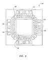
- FIG. 3is a top plan view of a leadframe
- FIGS. 4 - 9are side-elevation cross-sections of a preferred embodiment of the semiconductor package of the present invention from the initial to final construction.
- FIGS. 10 - 14are side-elevation cross-sections of an alternate embodiment of the semiconductor package of the present invention from the initial to final construction.
- FIGS. 1A and 1Bthere is shown a cross sectional illustration of one embodiment of a semiconductor package 10 construed in accordance with the principles of the present invention.
- the semiconductor package 10includes a corner 12 and bottom surface 15 .
- the semiconductor package 10further includes a semiconductor chip 20 having an upper surface 30 , a circumference 40 and a bottom surface 50 .
- a plurality of input bond pads 60 and output bond pads 70are disposed on the upper surface 30 of the semiconductor chip 20 .
- Conductive wires 75including but not limited to gold or aluminum wires, electrically connect the semiconductor chip 20 to the respective input bond pads 60 or output bond pads 70 .
- a chip paddle 80 having a upper surface 90 , a side surface 100 and a bottom surface 110is secured to the bottom surface 50 of the semiconductor chip 20 via an adhesive 120 .
- the chip paddle 80has corners 130 , a circumference 140 and may include a half-etched section 150 .
- the half-etched section 150is located at a lower edge 160 of the chip paddle 80 .
- a leadframe 170having a plurality of tie bars 180 and a side surface 190 .
- the tie bars 180are connected to the corners 130 of the chip paddle 80 and externally extend from the chip paddle 80 .
- the leadframe 170also includes a plurality of dam bars 220 .
- a plurality of leads 230are connected to the leadframe 170 and have an upper surface 235 , a side surface 240 and a bottom surface 250 .
- the leads 230are radially formed at regular intervals along the semiconductor chip circumference 40 and spaced apart from the circumference 40 of the semiconductor chip 20 .
- the leads 230extend towards the chip 20 and have a half-etched section 260 facing the chip 20 .
- the leads 230are radially formed at regular intervals along the chip paddle circumference 140 and spaced apart from the circumference 140 of the chip paddle 80 .
- the leads 230extend towards the chip paddle 80 , such that each of the plurality of leads 230 has a half-etched section 260 facing the chip paddle 80 .
- a ground ring 262formed in package 10 .
- the ground ring 262is positioned between the semiconductor chip 20 and the plurality of leads 230 , and may be interchangeably used as a power ring should circumstances require.
- Conductive wires 75can connect the ground ring 262 to the respective input bond pads 60 or output bond pads 70 , depending on the application.
- the upper surface 264 of the ground ring 262is planar with the upper surface 30 of the semiconductor chip 20 and the upper surface 235 of the leads 230 .
- the upper surface 264 of the ground ring 262may be planar with the upper surface of the chip paddle 80 to minimize package thickness.
- the upper surface 235 of the leads 230is planar with the upper surface 30 of the semiconductor chip 20 (FIGS. 1A and 1B) to minimize package thickness.
- the upper surface 235 of the leads 230is planar with the upper surface 90 of the chip paddle 80 to reduce package thickness.
- encapsulation material 280at least partially encapsulates the semiconductor chip 20 , conductive wires 70 , and leads 230 .
- the encapsulation material 280encapsulates the chip paddle 80 as well.
- the encapsulation material 280encapsulates the ground ring 262 .
- dam bars 220limit the flow of the encapsulation material 280 on the leadframe 170 and provide stability to the leads 230 on the leadframe 170 .
- the chip paddle 80 , leads 230 , and tie bars 180may be externally exposed at peripheral side and bottom surfaces.
- the externally exposed portions of chip paddle 80 , leads 230 , and tie bars 180may, but do no necessarily have to be, electroplated with corrosion-minimizing materials such as but not limited to, tin lead, tin, gold, nickel palladium, tin bismuth, or any other similar material known in the art.
- the respective half-etched sections 150 , 260 of the chip paddle 80 and leads 230are provided to increase the bonding strength of the encapsulation material 280 in the package 10 . It is contemplated that the respective half-etched sections 150 , 260 may be eliminated without departing from the scope and spirit of this invention.
- FIGS. 4 - 9in general, there is shown a cross-section of the semiconductor package 10 of FIG. 1A.
- the leadframealthough not shown in these figures, having leads 230 and a space 290 large enough to accommodate a semiconductor chip 20 , is first placed upon an adhesive tape 300 .
- a semiconductor chip 20is fixed to the adhesive tape 300 within the space 290 as best seen in FIG. 5.
- the semiconductor chip 20 and the leads 230are pressurized downwardly onto the tape 300 at a suitable temperature to make the tape 300 firmly adhere to the semiconductor chip 20 and leads 230 .
- the input bond pads 60 and output bond pads 70 of the semiconductor chip 20are next electrically connected to the leads 230 via conductive wires 75 .
- Upper surface 235 of leads 230may, but do not necessarily have to be, electroplated with a material that enhances electrical conductivity such as, for example, gold or silver.
- the conductive wires 75are connected via an automated process, but may be connected in any alternate method in the industry.
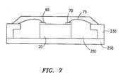
- the semiconductor chip 20 , conductive wires 75 , and leads 230are then at least partially encapsulated with the encapsulation material 280 , which may be an epoxy molding compound or a liquid encapsulation material, thereby forming a package body 10 as seen in FIG. 7.
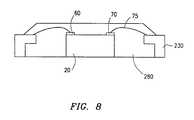
- the adhesive tape 300is next removed from the bottom surface 15 of the package 10 .
- the leads 230are next severed from the leadframe (not shown) by cutting through the dam bars (not shown) or neighboring areas of the package body 10 best seen in FIG. 9 as a singulation step. It is to be noted that this singulation step may occur before the adhesive tape 300 is removed.
- a marking process(not shown) may be carried out by the use of ink or lasers.
- the removal of the adhesive tape 300allows the semiconductor chip 20 and leads 240 to be exposed to the outside, thereby improving heat radiation.
- flasheswhich are typically formed during the molding process are not generated, thereby eliminating or reducing any further deflashing steps.
- a predetermined thickness of soldermay be plated over the bottom surface 250 of the of the leads 230 to allow easy fusion of the package 10 to a motherboard (not shown).
- FIGS. 10 - 14there are shown cross-sections of the semiconductor package 10 of FIG. 2A during various stages of construction. It is to be recognized that the method for constructing the semiconductor package 10 of FIG. 2A may be used for constructing the embodiment shown in FIG. 2B without departing from the principles of this invention.
- the leadframe(not shown) having leads 230 and a chip paddle 80 is first placed upon an adhesive tape 300 best seen in FIG. 10.
- the chip paddle 80 and the leads 230are pressurized downwardly onto the tape 300 at a suitable temperature to make the tape 300 firmly adhere to the chip paddle 80 and leads 230 .
- the semiconductor chip 20is bonded to the upper surface 90 of the chip paddle 80 via an adhesive 120 .
- the input pads 60 and output pads 70 of the semiconductor chip 20are next electrically connected to the leads 230 via conductive wires 75 .
- Upper surfaces 235 of leads 230may, but do not necessarily have to be, electroplated with a material that enhances electrical conductivity such as, for example, gold or silver.
- the conductive wires 75are connected via an automated process, but may also be connected in any alternate method in the industry.
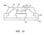
- the semiconductor chip 20 , chip paddle 80 , conductive wires 75 , and leads 230are then at least partially encapsulated with the encapsulation material 280 , which may be thermoplastics or thermoset resins, with thermoset resins including, for example, silicones, phenolics, and epoxies.
- the encapsulation material 280forms a package body 10 as seen in FIG. 12.
- the adhesive tape 300is next removed from the bottom surface 15 of the package 10 .
- the leads 230are next severed from the leadframe (not shown) by cutting through the dam bars (not shown) or neighboring areas of the package body 10 best seen in FIG. 14 in a singulation step. It is noted that this singulation step may occur before the adhesive tape 300 is removed.
- a marking processmay be carried out by the use of ink or lasers.
- the removal of the adhesive tape 300allows the chip paddle 80 and leads 230 to be exposed to the outside, thereby improving heat radiation.
- flasheswhich are typically formed during the molding process, are not generated, thereby eliminating or reducing any further deflashing steps.
- Bottom surfaces 110 , 250 of the chip paddle 80 and leads 230may be electroplated with corrosion-minimizing materials such as, but not limited to, tin lead, tin, gold, nickel palladium, tin bismuth, or other similar materials known in the art.
- a predetermined thickness of soldermay be plated over the bottom surface 250 of the of the leads 230 to allow easy fusion of the package 10 to a motherboard (not shown).
- the bottom surface 15 of the semiconductor chip 20is in the same plane as the bottom surface 250 of the leads 230 , so that the semiconductor package 10 is thin by limiting the height level of the conductive wires 75 .
- the direct exposure of the semiconductor chip 20provides for higher thermal radiation.
Landscapes
- Engineering & Computer Science (AREA)
- Physics & Mathematics (AREA)
- Condensed Matter Physics & Semiconductors (AREA)
- General Physics & Mathematics (AREA)
- Computer Hardware Design (AREA)
- Microelectronics & Electronic Packaging (AREA)
- Power Engineering (AREA)
- Manufacturing & Machinery (AREA)
- Geometry (AREA)
- Lead Frames For Integrated Circuits (AREA)
- Wire Bonding (AREA)
Abstract
Description
- 1. Technical Field of the Invention[0001]
- The present invention relates to a packaged semiconductor, a semiconductor package and a method for fabricating the package, and more particularly but not by way of limitation, to a thin semiconductor package having improvements in heat radiation and a method for manufacturing the same.[0002]
- 2. History of Related Art[0003]
- It is conventional in the electronic industry to encapsulate one or more semiconductor devices, such as integrated circuit dies, or chips, in a semiconductor package. These plastic packages protect a chip from environmental hazards, and provide a method of and apparatus for electrically and mechanically attaching the chip to an intended device. Recently, such semiconductor packages have included metal lead frames for supporting an integrated circuit chip which is bonded to a chip paddle region formed centrally therein. Bond wires which electrically connect pads on the integrated circuit chip to individual leads of the lead frame are then incorporated. A hard plastic encapsulating material, or encapsulant, which covers the bond wire, the integrated circuit chip and other components, forms the exterior of the package. A primary focus in this design is to provide the chip with adequate protection from the external environment in a reliable and effective manner.[0004]
- As set forth above, the semiconductor package therein described incorporates a lead frame as the central supporting structure of such a package. A portion of the lead frame completely surrounded by the plastic encapsulant is internal to the package. Portions of the lead frame extend internally from the package and are then used to connect the package externally. More information relative to lead frame technology may be found in Chapter 8 of the book[0005]Micro Electronics Packaging Handbook,(1989), edited by R. Tummala and E. Rymaszewski and incorporated by reference herein. This book is published by Van Nostrand Reinhold, 115 Fifth Avenue, New York, N.Y.
- Once the integrated circuit chips have been produced and encapsulated in semiconductor packages described above, they may be used in a wide variety of electronic appliances. The variety of electronic devices utilizing semiconductor packages has grown dramatically in recent years. These devices include cellular phones, portable computers, etc. Each of these devices typically include a motherboard on which a significant number of such semiconductor packages are secured to provide multiple electronic functions. These electronic appliances are typically manufactured in reduced sizes and at reduced costs, consumer demand increases. Accordingly, not only are semiconductor chips highly integrated, but also semiconductor packages are highly miniaturized with an increased level of package mounting density.[0006]
- According to such miniaturization tendencies, semiconductor packages, which transmit electrical signals from semiconductor chips to motherboards and support the semiconductor chips on the motherboards, have been designed to have a small size. By way of example only, such semiconductor packages may have a size on the order of 1×1 mm to 10×10 mm. Examples of such semiconductor packages are referred to as MLF (micro leadframe) type semiconductor packages and MLP (micro leadframe package) type semiconductor packages. Both MLF type semiconductor packages and MLP type semiconductor packages are generally manufactured in the same manner.[0007]
- Such conventional semiconductor packages are not without problems. Specifically, a typical semiconductor package is difficult to make slim because the thickness of the internal leads is equivalent to the thickness of the chip paddle. Further, the mounting of the semiconductor chip on the chip paddle increases the overall thickness of the package. The thickness is increased because of the input/output pads on the semiconductor chip mounted on the chip paddle are positioned at a higher level than the internal leads, thereby increasing the loop height of the conductive wires. The increased height may contribute to wire sweeping, caused by the encapsulation material during encapsulation.[0008]
- In addition, mounting the semiconductor chip on a chip paddle having an externally exposed bottom surface has poorer heat radiation than having a direct externally exposed bottom surface of the semiconductor chip.[0009]
- Finally, after the chip-mounting step and wire-bonding step are performed, the semiconductor package is encapsulated only after the leadframe is positioned on a mold. Thus, although the leadframe is in close contact with the lower mold die, some encapsulation material infiltrates through the interface between the leadframe and the lower mold die, resulting in the formation of so-called “flash”. An extra de-flashing step must then generally be executed.[0010]
- In one embodiment of the present invention, there is provided a semiconductor package comprising a semiconductor chip having an upper surface and a bottom surface. A plurality of input bond pads and output bond pads on the upper surface of the semiconductor chip and along the circumference of the semiconductor chip are electrically connected to the semiconductor chip. A chip paddle may be provided which has a top surface, a side surface and a bottom surface. The chip paddle is bonded to the bottom surface of the semiconductor chip by an adhesive. The chip paddle has corners, a circumference and a half-etched section at the lower edge of the chip paddle along the chip paddle circumference.[0011]
- A lead frame is provided having a plurality of tie bars. Each of the tie bars has a side surface and a bottom surface. The plurality of tie bars are connected to the corners of the chip paddle. The plurality of the tie bars externally extend from the chip paddle and have a half-etched section. A plurality of dam bars are provided on the lead frame help limit flow of encapsulation material on the leadframe.[0012]
- A plurality of internal leads connect to the leadframe. Each of the leads has a side surface and a bottom surface. The leads are radially formed at regular intervals along and spaced apart from the circumference to the chip paddle and extend towards the chip paddle. Each of the leads has a step shaped half-etched section facing the chip paddle.[0013]
- A plurality of via conductive wires are electrically connected to and between the plurality of leads and the semiconductor chip. Encapsulating material encapsulates the semiconductor chip, conductive wires, chip paddle, and the leads to form a package body. The flow of the encapsulation material is limited by the dam bars formed on the leadframe. The dam bars also serve to stabilize the leads on the leadframe. After encapsulation, the chip paddle, leads, and tie bars are externally exposed at respective side and bottom surfaces.[0014]
- A ground ring may be provided on the leadframe having an upper surface and a lower surface. The conductive wires may be connected to the ground ring, which is exposed at the lower surface. The ground ring may further serve to function as a power ring.[0015]
- A more complete understanding of the method and apparatus of the present invention may be obtained by reference to the following detailed description when taken in conjunction with the accompanying Drawings wherein:[0016]
- FIG. 1A is a cross-section of a semiconductor package made in accordance with one embodiment of the present invention;[0017]
- FIG. 1B is a cross-section of the semiconductor package of FIG. 1A with a ground ring included in the package;[0018]
- FIG. 2A is a cross-section of an alternate embodiment of a semiconductor package made in accordance with the teachings of the present invention;[0019]
- FIG. 2B is a cross-section of the semiconductor package of FIG. 2A with a ground ring included in the package;[0020]
- FIG. 3 is a top plan view of a leadframe;[0021]
- FIGS.[0022]4-9 are side-elevation cross-sections of a preferred embodiment of the semiconductor package of the present invention from the initial to final construction; and
- FIGS.[0023]10-14 are side-elevation cross-sections of an alternate embodiment of the semiconductor package of the present invention from the initial to final construction.
- Referring first to FIGS. 1A and 1B, there is shown a cross sectional illustration of one embodiment of a[0024]
semiconductor package 10 construed in accordance with the principles of the present invention. Thesemiconductor package 10 includes acorner 12 andbottom surface 15. Thesemiconductor package 10 further includes asemiconductor chip 20 having anupper surface 30, acircumference 40 and abottom surface 50. A plurality ofinput bond pads 60 andoutput bond pads 70 are disposed on theupper surface 30 of thesemiconductor chip 20.Conductive wires 75, including but not limited to gold or aluminum wires, electrically connect thesemiconductor chip 20 to the respectiveinput bond pads 60 oroutput bond pads 70. - In an alternate embodiment best seen in FIGS. 2A and 2B, a[0025]
chip paddle 80 having aupper surface 90, aside surface 100 and abottom surface 110 is secured to thebottom surface 50 of thesemiconductor chip 20 via an adhesive120. Thechip paddle 80 hascorners 130, acircumference 140 and may include a half-etchedsection 150. The half-etchedsection 150 is located at alower edge 160 of thechip paddle 80. - Referring now to FIG. 3, a[0026]
leadframe 170 is shown having a plurality of tie bars180 and aside surface 190. The tie bars180 are connected to thecorners 130 of thechip paddle 80 and externally extend from thechip paddle 80. Theleadframe 170 also includes a plurality of dam bars220. - A plurality of[0027]
leads 230 are connected to theleadframe 170 and have anupper surface 235, aside surface 240 and abottom surface 250. In a first embodiment seen in FIGS. 1A and 1B, theleads 230 are radially formed at regular intervals along thesemiconductor chip circumference 40 and spaced apart from thecircumference 40 of thesemiconductor chip 20. The leads230 extend towards thechip 20 and have a half-etchedsection 260 facing thechip 20. - In an alternate embodiment best seen in FIGS. 2A and 2B, the[0028]
leads 230 are radially formed at regular intervals along thechip paddle circumference 140 and spaced apart from thecircumference 140 of thechip paddle 80. The leads230 extend towards thechip paddle 80, such that each of the plurality ofleads 230 has a half-etchedsection 260 facing thechip paddle 80. - Referring back to FIGS. 1B and 2B, there is shown a[0029]
ground ring 262 formed inpackage 10. Theground ring 262 is positioned between thesemiconductor chip 20 and the plurality ofleads 230, and may be interchangeably used as a power ring should circumstances require.Conductive wires 75 can connect theground ring 262 to the respectiveinput bond pads 60 oroutput bond pads 70, depending on the application. As seen in FIG. 1B, theupper surface 264 of theground ring 262 is planar with theupper surface 30 of thesemiconductor chip 20 and theupper surface 235 of theleads 230. However, as seen in FIG. 2B, theupper surface 264 of theground ring 262 may be planar with the upper surface of thechip paddle 80 to minimize package thickness. Likewise, theupper surface 235 of theleads 230 is planar with theupper surface 30 of the semiconductor chip20 (FIGS. 1A and 1B) to minimize package thickness. In the alternate embodiments shown in FIGS. 2A and 2B, theupper surface 235 of theleads 230 is planar with theupper surface 90 of thechip paddle 80 to reduce package thickness. - Referring generally now to FIGS. 1A and 3, to enclose the[0030]
semiconductor package 10,encapsulation material 280 at least partially encapsulates thesemiconductor chip 20,conductive wires 70, and leads230. In the alternate embodiment shown in FIGS. 2A and 2B, theencapsulation material 280 encapsulates thechip paddle 80 as well. Likewise, for the embodiments shown in FIGS. 1B and 2B, theencapsulation material 280 encapsulates theground ring 262. - Referring now to FIGS. 1 through 3 in general, dam bars[0031]220 limit the flow of the
encapsulation material 280 on theleadframe 170 and provide stability to theleads 230 on theleadframe 170. In the respective embodiment during encapsulation, thechip paddle 80, leads230, and tiebars 180 may be externally exposed at peripheral side and bottom surfaces. The externally exposed portions ofchip paddle 80, leads230, and tiebars 180 may, but do no necessarily have to be, electroplated with corrosion-minimizing materials such as but not limited to, tin lead, tin, gold, nickel palladium, tin bismuth, or any other similar material known in the art. The respective half-etchedsections chip paddle 80 and leads230 are provided to increase the bonding strength of theencapsulation material 280 in thepackage 10. It is contemplated that the respective half-etchedsections - Referring now to FIGS.[0032]4-9 in general, there is shown a cross-section of the
semiconductor package 10 of FIG. 1A. It is to be recognized that the method for constructing thesemiconductor package 10 of FIG. 1A may be used for constructing the embodiment shown in FIG. 1B without departing from the principles of this invention. The leadframe, although not shown in these figures, having leads230 and a space290 large enough to accommodate asemiconductor chip 20, is first placed upon an adhesive tape300. Next, asemiconductor chip 20 is fixed to the adhesive tape300 within the space290 as best seen in FIG. 5. Thesemiconductor chip 20 and theleads 230 are pressurized downwardly onto the tape300 at a suitable temperature to make the tape300 firmly adhere to thesemiconductor chip 20 and leads230. - As shown in FIG. 6, the[0033]
input bond pads 60 andoutput bond pads 70 of thesemiconductor chip 20 are next electrically connected to theleads 230 viaconductive wires 75.Upper surface 235 ofleads 230 may, but do not necessarily have to be, electroplated with a material that enhances electrical conductivity such as, for example, gold or silver. Typically, theconductive wires 75 are connected via an automated process, but may be connected in any alternate method in the industry. - The[0034]
semiconductor chip 20,conductive wires 75, and leads230 are then at least partially encapsulated with theencapsulation material 280, which may be an epoxy molding compound or a liquid encapsulation material, thereby forming apackage body 10 as seen in FIG. 7. Referring to FIG. 8, the adhesive tape300 is next removed from thebottom surface 15 of thepackage 10. The leads230 are next severed from the leadframe (not shown) by cutting through the dam bars (not shown) or neighboring areas of thepackage body 10 best seen in FIG. 9 as a singulation step. It is to be noted that this singulation step may occur before the adhesive tape300 is removed. - After formation of the[0035]
package body 10, a marking process (not shown) may be carried out by the use of ink or lasers. The removal of the adhesive tape300 allows thesemiconductor chip 20 and leads240 to be exposed to the outside, thereby improving heat radiation. By adhering theadhesive tape 250 to the bottom surfaces15,250 of thesemiconductor chip 20 and leads230, respectively, flashes, which are typically formed during the molding process are not generated, thereby eliminating or reducing any further deflashing steps. - After the removal of the adhesive tape[0036]300, a predetermined thickness of solder (not shown) may be plated over the
bottom surface 250 of the of theleads 230 to allow easy fusion of thepackage 10 to a motherboard (not shown). - Referring now generally to FIGS.[0037]10-14, there are shown cross-sections of the
semiconductor package 10 of FIG. 2A during various stages of construction. It is to be recognized that the method for constructing thesemiconductor package 10 of FIG. 2A may be used for constructing the embodiment shown in FIG. 2B without departing from the principles of this invention. The leadframe (not shown) having leads230 and achip paddle 80 is first placed upon an adhesive tape300 best seen in FIG. 10. Thechip paddle 80 and theleads 230 are pressurized downwardly onto the tape300 at a suitable temperature to make the tape300 firmly adhere to thechip paddle 80 and leads230. - As shown in FIG. 11, the[0038]
semiconductor chip 20 is bonded to theupper surface 90 of thechip paddle 80 via an adhesive120. Theinput pads 60 andoutput pads 70 of thesemiconductor chip 20 are next electrically connected to theleads 230 viaconductive wires 75.Upper surfaces 235 ofleads 230 may, but do not necessarily have to be, electroplated with a material that enhances electrical conductivity such as, for example, gold or silver. Typically, theconductive wires 75 are connected via an automated process, but may also be connected in any alternate method in the industry. - The[0039]
semiconductor chip 20,chip paddle 80,conductive wires 75, and leads230 are then at least partially encapsulated with theencapsulation material 280, which may be thermoplastics or thermoset resins, with thermoset resins including, for example, silicones, phenolics, and epoxies. Theencapsulation material 280 forms apackage body 10 as seen in FIG. 12. - Referring to FIG. 13, the adhesive tape[0040]300 is next removed from the
bottom surface 15 of thepackage 10. The leads230 are next severed from the leadframe (not shown) by cutting through the dam bars (not shown) or neighboring areas of thepackage body 10 best seen in FIG. 14 in a singulation step. It is noted that this singulation step may occur before the adhesive tape300 is removed. - Once the[0041]
package body 10 is formed, a marking process (not shown) may be carried out by the use of ink or lasers. The removal of the adhesive tape300 allows thechip paddle 80 and leads230 to be exposed to the outside, thereby improving heat radiation. By adhering the adhesive tape300 to the bottom surfaces110,250 of thechip paddle 80 and leads230, respectively, flashes, which are typically formed during the molding process, are not generated, thereby eliminating or reducing any further deflashing steps. Bottom surfaces110,250 of thechip paddle 80 and leads230, may be electroplated with corrosion-minimizing materials such as, but not limited to, tin lead, tin, gold, nickel palladium, tin bismuth, or other similar materials known in the art. - After the removal of the tape[0042]300, a predetermined thickness of solder (not shown) may be plated over the
bottom surface 250 of the of theleads 230 to allow easy fusion of thepackage 10 to a motherboard (not shown). - In such a semiconductor package as described and shown in FIGS. 1A and 1B, the[0043]
bottom surface 15 of thesemiconductor chip 20 is in the same plane as thebottom surface 250 of theleads 230, so that thesemiconductor package 10 is thin by limiting the height level of theconductive wires 75. In addition, the direct exposure of thesemiconductor chip 20 provides for higher thermal radiation. - The following applications are all being filed on the same date as the present application and all are incorporated by reference as if wholly rewritten entirely herein:[0044]
Attorney First Named Docket No. Title of Application Inventor 45475-00014 Lead Frame for Semiconductor Young Suk Package and Mold for Molding the Chung Same 45475-00017 Method for Making a Semiconductor Tae Heon Lee Package Having Improved Defect Testing and Increased Production Yield 45475-00018 Near Chip Size Semiconductor Sean Timothy Package Crowley 45475-00022 End Grind Array Semiconductor Jae Hun Ku Package 45475-00026 Leadframe and Semiconductor Package Tae Heon Lee with Improved Solder Joint Strength 45475-00027 Semiconductor Package Having Tae Heon Lee Reduced Thickness 45475-00029 Semiconductor Package Leadframe Young Suk Assembly and Method of Manufacture Chung 45475-00030 Semiconductor Package and Method Young Suk Thereof Chung - It is thus believed that the operation and construction of the present invention will be apparent from the foregoing description of the preferred exemplary embodiments. It will be obvious to a person of ordinary skill in the art that various changes and modifications may be made herein without departing from the spirit and the scope of the invention.[0045]
Claims (16)
1. A packaged semiconductor, comprising:
a semiconductor chip having a planar upper surface, a circumference and a bottom surface;
a plurality of input bond pads on the planar upper surface of said semiconductor chip along the circumference and electrically connected to said semiconductor chip;
a plurality of output bond pads on the planar upper surface along the circumference of said semiconductor chip and electrically connected to said semiconductor chip;
a leadframe having a plurality of tie bars, said tie bars having a side surface and a bottom surface, said leadframe having a plurality of dam bars;
a plurality of internal leads connected to said leadframe, said plurality of internal leads having a side surface and a bottom surface, said plurality of internal leads being radially formed at regular intervals along and spaced apart from said circumference of said semiconductor chip and extending towards said semiconductor chip, each of said plurality of internal leads having a half-etched section facing said semiconductor chip, each of said plurality of leads having an upper surface in the plane of said upper surface of said semiconductor chip;
a plurality of conductive wires for electrically connecting to said plurality of internal leads and to said semiconductor chip;
encapsulant material encapsulating said semiconductor chip, said plurality of conductive wires, and said plurality of internal leads to form a package body, wherein flow of said encapsulant material is limited by said plurality of dam bars formed on said leadframe; and
wherein said semiconductor chip, said plurality of internal leads and said plurality of tie bars are externally exposed at respective side and bottom surface.
2. The semiconductor package ofclaim 1 , further comprising
a chip paddle connected to said leadframe, said chip paddle having a top surface, a side surface and a bottom surface, said chip paddle bonded to said bottom surface of said semiconductor chip by an adhesive, said chip paddle having corners, a circumference and a half-etched section at a lower edge of said chip paddle along said chip paddle circumference.
3. The semiconductor package ofclaim 2 , wherein each of said plurality of tie bars are connected to said corners of said chip paddle.
4. The semiconductor package ofclaim 3 , wherein each of said plurality of tie bars has a half-etched section, and whereas each of said plurality of tie bars externally extend from said chip paddle.
5. A packaged semiconductor, comprising:
a leadframe having a plurality of tie bars, said tie bars having a side surface and a bottom surface, said leadframe having a plurality of dam bars and a space for receiving a semiconductor chip;
a plurality of internal leads connected to said leadframe, said plurality of internal leads having a side surface and a bottom surface, said plurality of internal leads being radially formed at regular intervals along and spaced apart from said circumference of said semiconductor chip and extending towards said semiconductor chip, each of said plurality of internal leads having a half-etched section facing said semiconductor chip, each of said plurality of leads having an upper surface in the plane of said upper surface of said semiconductor chip;
a plurality of conductive wires for electrically connecting to said plurality of internal leads and to said semiconductor chip;
encapsulant material encapsulating said semiconductor chip, said plurality of conductive wires, and said plurality of internal leads to form a package body, wherein flow of said encapsulant material is limited by said plurality of dam bars formed on said leadframe; and
wherein said semiconductor chip, said plurality of internal leads and said plurality of tie bars are externally exposed at respective side and bottom surface.
6. The semiconductor package ofclaim 5 , further comprising:
a semiconductor chip having a planar upper surface, a circumference and a bottom surface secured into said space on said leadframe.
7. The semiconductor package ofclaim 6 , further comprising:
a plurality of input bond pads on the planar upper surface of said semiconductor chip along the circumference and electrically connected to said semiconductor chip; and
a plurality of output bond pads on the planar upper surface along the circumference of said semiconductor chip and electrically connected to said semiconductor chip;
8. The semiconductor package ofclaim 7 , further comprising
a chip paddle connected to said leadframe, said chip paddle having a top surface, a side surface and a bottom surface, said chip paddle bonded to said bottom surface of said semiconductor chip by an adhesive, said chip paddle having corners, a circumference and a half-etched section at a lower edge of said chip paddle along said chip paddle circumference.
9. The semiconductor package ofclaim 8 , wherein each of said plurality of tie bars are connected to said corners of said chip paddle.
10. The semiconductor package ofclaim 9 , wherein each of said plurality of tie bars has a half-etched section, and whereas each of said plurality of tie bars externally extend from said chip paddle.
11. A method for making a semiconductor package, comprising the steps of:
placing a leadframe having a plurality of leads and a space for accommodating a semiconductor chip on an adhesive tape, said plurality of leads having a bottom surface;
affixing a semiconductor chip having a bottom surface, input bond pads and output bond pads within said space on said leadframe;
pressurizing said leadframe and said semiconductor chip downwardly onto said tape;
electrically connecting said input bond pads and said output bond pads of said semiconductor chip to said leads via wires;
encapsulating said semiconductor chip, said wires, and said leads by an encapsulant material to form a package body;
removing said adhesive tape from said package body while leaving said bottom surface of said leads and said bottom surface of said semiconductor chip externally exposed; and
cutting said package from said leadframe.
12. The method as inclaim 11 , wherein the steps are performed sequentially.
13. A method for making a packaged semiconductor, comprising the steps of:
placing a leadframe having a plurality of leads, a ground ring having a bottom surface, and a space for accommodating a semiconductor chip on an adhesive tape, said plurality of leads having a bottom surface;
affixing a semiconductor chip having a bottom surface, input bond pads and output bond pads within said space on said leadframe;
electrically connecting said input bond pads and said output bond pads of said semiconductor chip to said leads via wires;
encapsulating said semiconductor chip, said ground ring, said wires, and said leads by an encapsulant material to form a package body;
removing said adhesive tape from said package body while leaving said bottom surface of said leads, said bottom surface of said ground ring, and said bottom surface of said semiconductor chip externally exposed; and
cutting said package from said leadframe.
14. The method as inclaim 13 , wherein the steps are performed sequentially.
15. A method for making a packaged semiconductor, comprising the steps of:
placing a leadframe having a chip paddle having a bottom surface and a plurality of leads on an adhesive tape, said plurality of leads having a bottom surface;
affixing a semiconductor chip having a bottom surface, input bond pads and output bond pads onto said chip paddle via an adhesive;
electrically connecting said input bond pads and said output bond pads of said semiconductor chip to said leads via wires;
encapsulating said semiconductor chip, said wires, and said leads by an encapsulant material to form a package body;
removing said adhesive tape from said package body while leaving said bottom surface of said leads and said bottom surface of said semiconductor chip externally exposed; and
cutting said package from said leadframe.
16. The method as inclaim 15 , wherein the steps are performed sequentially.
Priority Applications (1)
| Application Number | Priority Date | Filing Date | Title |
|---|---|---|---|
| US10/665,651US20040061217A1 (en) | 1999-10-15 | 2003-09-19 | Thin and heat radiant semiconductor package and method for manufacturing |
Applications Claiming Priority (4)
| Application Number | Priority Date | Filing Date | Title |
|---|---|---|---|
| KR99-44655/9150 | 1999-10-15 | ||
| KR19990044655 | 1999-10-15 | ||
| US09/687,787US6646339B1 (en) | 1999-10-15 | 2000-10-13 | Thin and heat radiant semiconductor package and method for manufacturing |
| US10/665,651US20040061217A1 (en) | 1999-10-15 | 2003-09-19 | Thin and heat radiant semiconductor package and method for manufacturing |
Related Parent Applications (1)
| Application Number | Title | Priority Date | Filing Date |
|---|---|---|---|
| US09/687,787DivisionUS6646339B1 (en) | 1999-10-15 | 2000-10-13 | Thin and heat radiant semiconductor package and method for manufacturing |
Publications (1)
| Publication Number | Publication Date |
|---|---|
| US20040061217A1true US20040061217A1 (en) | 2004-04-01 |
Family
ID=19615438
Family Applications (2)
| Application Number | Title | Priority Date | Filing Date |
|---|---|---|---|
| US09/687,787Expired - LifetimeUS6646339B1 (en) | 1999-10-15 | 2000-10-13 | Thin and heat radiant semiconductor package and method for manufacturing |
| US10/665,651AbandonedUS20040061217A1 (en) | 1999-10-15 | 2003-09-19 | Thin and heat radiant semiconductor package and method for manufacturing |
Family Applications Before (1)
| Application Number | Title | Priority Date | Filing Date |
|---|---|---|---|
| US09/687,787Expired - LifetimeUS6646339B1 (en) | 1999-10-15 | 2000-10-13 | Thin and heat radiant semiconductor package and method for manufacturing |
Country Status (3)
| Country | Link |
|---|---|
| US (2) | US6646339B1 (en) |
| KR (1) | KR100526844B1 (en) |
| SG (1) | SG92748A1 (en) |
Cited By (6)
| Publication number | Priority date | Publication date | Assignee | Title |
|---|---|---|---|---|
| US20040159919A1 (en)* | 2003-02-18 | 2004-08-19 | Hitachi, Ltd. | Electronic circuit device |
| US6853059B1 (en)* | 1999-10-15 | 2005-02-08 | Amkor Technology, Inc. | Semiconductor package having improved adhesiveness and ground bonding |
| US20060175689A1 (en)* | 2005-02-08 | 2006-08-10 | Stats Chippac Ltd. | Multi-leadframe semiconductor package and method of manufacture |
| US20070114641A1 (en)* | 2005-11-21 | 2007-05-24 | Stmicroelectronics Asia Pacific Pte Ltd | Ultra-thin quad flat no-lead (QFN) package |
| US20080142938A1 (en)* | 2006-12-13 | 2008-06-19 | Stats Chippac Ltd. | Integrated circuit package system employing a support structure with a recess |
| US20090224380A1 (en)* | 2008-03-04 | 2009-09-10 | Powertech Technology Inc. | Leadframe and semiconductor package having downset baffle paddles |
Families Citing this family (63)
| Publication number | Priority date | Publication date | Assignee | Title |
|---|---|---|---|---|
| US6143981A (en) | 1998-06-24 | 2000-11-07 | Amkor Technology, Inc. | Plastic integrated circuit package and method and leadframe for making the package |
| US7332375B1 (en) | 1998-06-24 | 2008-02-19 | Amkor Technology, Inc. | Method of making an integrated circuit package |
| US6700185B1 (en) | 1999-11-10 | 2004-03-02 | Hitachi Chemical Co., Ltd. | Adhesive film for semiconductor, lead frame and semiconductor device using the same, and method for manufacturing semiconductor device |
| JP3895570B2 (en)* | 2000-12-28 | 2007-03-22 | 株式会社ルネサステクノロジ | Semiconductor device |
| US6734536B2 (en)* | 2001-01-12 | 2004-05-11 | Rohm Co., Ltd. | Surface-mounting semiconductor device and method of making the same |
| KR100369393B1 (en)* | 2001-03-27 | 2003-02-05 | 앰코 테크놀로지 코리아 주식회사 | Lead frame and semiconductor package using it and its manufacturing method |
| JP2004071670A (en)* | 2002-08-02 | 2004-03-04 | Fuji Photo Film Co Ltd | Ic package, connecting structure and electronic apparatus |
| US6903448B1 (en)* | 2002-11-12 | 2005-06-07 | Marvell International Ltd. | High performance leadframe in electronic package |
| US20040124508A1 (en)* | 2002-11-27 | 2004-07-01 | United Test And Assembly Test Center Ltd. | High performance chip scale leadframe package and method of manufacturing the package |
| US20040130007A1 (en)* | 2003-01-06 | 2004-07-08 | Cheng-Ho Hsu | Flat lead package for a semiconductor device |
| US7153724B1 (en)* | 2003-08-08 | 2006-12-26 | Ns Electronics Bangkok (1993) Ltd. | Method of fabricating no-lead package for semiconductor die with half-etched leadframe |
| CN101587869B (en)* | 2003-08-26 | 2011-04-13 | 宇芯(毛里求斯)控股有限公司 | Reversible leadless package and methods of making and using same |
| US6977431B1 (en)* | 2003-11-05 | 2005-12-20 | Amkor Technology, Inc. | Stackable semiconductor package and manufacturing method thereof |
| US7144517B1 (en) | 2003-11-07 | 2006-12-05 | Amkor Technology, Inc. | Manufacturing method for leadframe and for semiconductor package using the leadframe |
| CN1331221C (en)* | 2003-12-19 | 2007-08-08 | 威宇科技测试封装有限公司 | Chip ball grid array packaging structure |
| WO2006090304A1 (en)* | 2005-02-23 | 2006-08-31 | Nxp B.V. | An integrated circuit package device with improved bond pad connections, a leadframe and an electronic device |
| TWM279015U (en)* | 2005-04-26 | 2005-10-21 | Lingsen Precision Ind Ltd | Metal leadframes for integrated circuits with different thickness of pins |
| US7507603B1 (en) | 2005-12-02 | 2009-03-24 | Amkor Technology, Inc. | Etch singulated semiconductor package |
| US7468548B2 (en)* | 2005-12-09 | 2008-12-23 | Fairchild Semiconductor Corporation | Thermal enhanced upper and dual heat sink exposed molded leadless package |
| DE102005062344B4 (en)* | 2005-12-23 | 2010-08-19 | Infineon Technologies Ag | Semiconductor component for high-frequency applications and method for producing such a semiconductor component |
| US7968998B1 (en) | 2006-06-21 | 2011-06-28 | Amkor Technology, Inc. | Side leaded, bottom exposed pad and bottom exposed lead fusion quad flat semiconductor package |
| US7977774B2 (en) | 2007-07-10 | 2011-07-12 | Amkor Technology, Inc. | Fusion quad flat semiconductor package |
| US7687899B1 (en) | 2007-08-07 | 2010-03-30 | Amkor Technology, Inc. | Dual laminate package structure with embedded elements |
| US7777351B1 (en) | 2007-10-01 | 2010-08-17 | Amkor Technology, Inc. | Thin stacked interposer package |
| US8089159B1 (en) | 2007-10-03 | 2012-01-03 | Amkor Technology, Inc. | Semiconductor package with increased I/O density and method of making the same |
| US7847386B1 (en) | 2007-11-05 | 2010-12-07 | Amkor Technology, Inc. | Reduced size stacked semiconductor package and method of making the same |
| US7956453B1 (en) | 2008-01-16 | 2011-06-07 | Amkor Technology, Inc. | Semiconductor package with patterning layer and method of making same |
| US7723852B1 (en) | 2008-01-21 | 2010-05-25 | Amkor Technology, Inc. | Stacked semiconductor package and method of making same |
| US8067821B1 (en) | 2008-04-10 | 2011-11-29 | Amkor Technology, Inc. | Flat semiconductor package with half package molding |
| US7768135B1 (en) | 2008-04-17 | 2010-08-03 | Amkor Technology, Inc. | Semiconductor package with fast power-up cycle and method of making same |
| US7808084B1 (en) | 2008-05-06 | 2010-10-05 | Amkor Technology, Inc. | Semiconductor package with half-etched locking features |
| US8125064B1 (en) | 2008-07-28 | 2012-02-28 | Amkor Technology, Inc. | Increased I/O semiconductor package and method of making same |
| US8184453B1 (en) | 2008-07-31 | 2012-05-22 | Amkor Technology, Inc. | Increased capacity semiconductor package |
| JP5493323B2 (en)* | 2008-09-30 | 2014-05-14 | 凸版印刷株式会社 | Manufacturing method of lead frame type substrate |
| US7847392B1 (en) | 2008-09-30 | 2010-12-07 | Amkor Technology, Inc. | Semiconductor device including leadframe with increased I/O |
| US7989933B1 (en) | 2008-10-06 | 2011-08-02 | Amkor Technology, Inc. | Increased I/O leadframe and semiconductor device including same |
| US8008758B1 (en) | 2008-10-27 | 2011-08-30 | Amkor Technology, Inc. | Semiconductor device with increased I/O leadframe |
| US8089145B1 (en) | 2008-11-17 | 2012-01-03 | Amkor Technology, Inc. | Semiconductor device including increased capacity leadframe |
| US8072050B1 (en) | 2008-11-18 | 2011-12-06 | Amkor Technology, Inc. | Semiconductor device with increased I/O leadframe including passive device |
| US7875963B1 (en) | 2008-11-21 | 2011-01-25 | Amkor Technology, Inc. | Semiconductor device including leadframe having power bars and increased I/O |
| US7982298B1 (en) | 2008-12-03 | 2011-07-19 | Amkor Technology, Inc. | Package in package semiconductor device |
| US8487420B1 (en) | 2008-12-08 | 2013-07-16 | Amkor Technology, Inc. | Package in package semiconductor device with film over wire |
| US8680656B1 (en) | 2009-01-05 | 2014-03-25 | Amkor Technology, Inc. | Leadframe structure for concentrated photovoltaic receiver package |
| US20170117214A1 (en) | 2009-01-05 | 2017-04-27 | Amkor Technology, Inc. | Semiconductor device with through-mold via |
| US8058715B1 (en) | 2009-01-09 | 2011-11-15 | Amkor Technology, Inc. | Package in package device for RF transceiver module |
| US8026589B1 (en) | 2009-02-23 | 2011-09-27 | Amkor Technology, Inc. | Reduced profile stackable semiconductor package |
| US7960818B1 (en) | 2009-03-04 | 2011-06-14 | Amkor Technology, Inc. | Conformal shield on punch QFN semiconductor package |
| US8575742B1 (en) | 2009-04-06 | 2013-11-05 | Amkor Technology, Inc. | Semiconductor device with increased I/O leadframe including power bars |
| KR101796116B1 (en) | 2010-10-20 | 2017-11-10 | 삼성전자 주식회사 | Semiconductor device, memory module and memory system having the same and operating method thereof |
| US8674485B1 (en) | 2010-12-08 | 2014-03-18 | Amkor Technology, Inc. | Semiconductor device including leadframe with downsets |
| TWI557183B (en) | 2015-12-16 | 2016-11-11 | 財團法人工業技術研究院 | Oxane composition, and photovoltaic device comprising the same |
| US8648450B1 (en) | 2011-01-27 | 2014-02-11 | Amkor Technology, Inc. | Semiconductor device including leadframe with a combination of leads and lands |
| KR101250529B1 (en)* | 2011-06-08 | 2013-04-03 | 에스티에스반도체통신 주식회사 | QFN(Quad Flat No-leads) package and the method of fabricating the same |
| JP5953703B2 (en)* | 2011-10-31 | 2016-07-20 | ソニー株式会社 | Lead frame and semiconductor device |
| KR101297015B1 (en)* | 2011-11-03 | 2013-08-14 | 주식회사 네패스 | Method of manufacturing fan-out semiconductor package using lead frame, semiconductor package thereof, and package on package thereof |
| US9704725B1 (en) | 2012-03-06 | 2017-07-11 | Amkor Technology, Inc. | Semiconductor device with leadframe configured to facilitate reduced burr formation |
| KR101486790B1 (en) | 2013-05-02 | 2015-01-28 | 앰코 테크놀로지 코리아 주식회사 | Micro Lead Frame for semiconductor package |
| KR101563911B1 (en) | 2013-10-24 | 2015-10-28 | 앰코 테크놀로지 코리아 주식회사 | Semiconductor package |
| US9673122B2 (en) | 2014-05-02 | 2017-06-06 | Amkor Technology, Inc. | Micro lead frame structure having reinforcing portions and method |
| US9082760B2 (en)* | 2014-06-16 | 2015-07-14 | Chang Wah Technology Co., Ltd. | Dual layered lead frame |
| US9263299B2 (en) | 2014-07-02 | 2016-02-16 | Nxp B.V. | Exposed die clip bond power package |
| CN105405823A (en)* | 2014-08-20 | 2016-03-16 | 飞思卡尔半导体公司 | Semiconductor device with inspectable solder joints |
| CN108417498A (en)* | 2018-03-14 | 2018-08-17 | 中国电子科技集团公司第五十八研究所 | Chip packaging method and chip packaging |
Citations (95)
| Publication number | Priority date | Publication date | Assignee | Title |
|---|---|---|---|---|
| US2596993A (en)* | 1949-01-13 | 1952-05-20 | United Shoe Machinery Corp | Method and mold for covering of eyelets by plastic injection |
| US3435815A (en)* | 1966-07-15 | 1969-04-01 | Micro Tech Mfg Inc | Wafer dicer |
| US3734660A (en)* | 1970-01-09 | 1973-05-22 | Tuthill Pump Co | Apparatus for fabricating a bearing device |
| US3838984A (en)* | 1973-04-16 | 1974-10-01 | Sperry Rand Corp | Flexible carrier and interconnect for uncased ic chips |
| US4054238A (en)* | 1976-03-23 | 1977-10-18 | Western Electric Company, Inc. | Method, apparatus and lead frame for assembling leads with terminals on a substrate |
| US4189342A (en)* | 1971-10-07 | 1980-02-19 | U.S. Philips Corporation | Semiconductor device comprising projecting contact layers |
| US4258381A (en)* | 1977-12-07 | 1981-03-24 | Steag, Kernergie Gmbh | Lead frame for a semiconductor device suitable for mass production |
| US4289922A (en)* | 1979-09-04 | 1981-09-15 | Plessey Incorporated | Integrated circuit package and lead frame |
| US4301464A (en)* | 1978-08-02 | 1981-11-17 | Hitachi, Ltd. | Lead frame and semiconductor device employing the same with improved arrangement of supporting leads for securing the semiconductor supporting member |
| US4332537A (en)* | 1978-07-17 | 1982-06-01 | Dusan Slepcevic | Encapsulation mold with removable cavity plates |
| US4417266A (en)* | 1981-08-14 | 1983-11-22 | Amp Incorporated | Power and ground plane structure for chip carrier |
| US4451224A (en)* | 1982-03-25 | 1984-05-29 | General Electric Company | Mold device for making plastic articles from resin |
| US4530152A (en)* | 1982-04-01 | 1985-07-23 | Compagnie Industrielle Des Telecommunications Cit-Alcatel | Method for encapsulating semiconductor components using temporary substrates |
| US4541003A (en)* | 1978-12-27 | 1985-09-10 | Hitachi, Ltd. | Semiconductor device including an alpha-particle shield |
| US4646710A (en)* | 1982-09-22 | 1987-03-03 | Crystal Systems, Inc. | Multi-wafer slicing with a fixed abrasive |
| US4707724A (en)* | 1984-06-04 | 1987-11-17 | Hitachi, Ltd. | Semiconductor device and method of manufacturing thereof |
| US4727633A (en)* | 1985-08-08 | 1988-03-01 | Tektronix, Inc. | Method of securing metallic members together |
| US4737839A (en)* | 1984-03-19 | 1988-04-12 | Trilogy Computer Development Partners, Ltd. | Semiconductor chip mounting system |
| US4756080A (en)* | 1986-01-27 | 1988-07-12 | American Microsystems, Inc. | Metal foil semiconductor interconnection method |
| US4812896A (en)* | 1986-11-13 | 1989-03-14 | Olin Corporation | Metal electronic package sealed with thermoplastic having a grafted metal deactivator and antioxidant |
| US4862245A (en)* | 1985-04-18 | 1989-08-29 | International Business Machines Corporation | Package semiconductor chip |
| US4862246A (en)* | 1984-09-26 | 1989-08-29 | Hitachi, Ltd. | Semiconductor device lead frame with etched through holes |
| US4907067A (en)* | 1988-05-11 | 1990-03-06 | Texas Instruments Incorporated | Thermally efficient power device package |
| US4920074A (en)* | 1987-02-25 | 1990-04-24 | Hitachi, Ltd. | Surface mount plastic package semiconductor integrated circuit, manufacturing method thereof, as well as mounting method and mounted structure thereof |
| US4935803A (en)* | 1988-09-09 | 1990-06-19 | Motorola, Inc. | Self-centering electrode for power devices |
| US4942454A (en)* | 1987-08-05 | 1990-07-17 | Mitsubishi Denki Kabushiki Kaisha | Resin sealed semiconductor device |
| US4987475A (en)* | 1988-02-29 | 1991-01-22 | Digital Equipment Corporation | Alignment of leads for ceramic integrated circuit packages |
| US5018003A (en)* | 1988-10-20 | 1991-05-21 | Mitsubishi Denki Kabushiki Kaisha | Lead frame and semiconductor device |
| US5029386A (en)* | 1990-09-17 | 1991-07-09 | Hewlett-Packard Company | Hierarchical tape automated bonding method |
| US5041902A (en)* | 1989-12-14 | 1991-08-20 | Motorola, Inc. | Molded electronic package with compression structures |
| US5057900A (en)* | 1988-10-17 | 1991-10-15 | Semiconductor Energy Laboratory Co., Ltd. | Electronic device and a manufacturing method for the same |
| US5059379A (en)* | 1987-07-20 | 1991-10-22 | Mitsubishi Denki Kabushiki Kaisha | Method of resin sealing semiconductor devices |
| US5065223A (en)* | 1989-05-31 | 1991-11-12 | Fujitsu Vlsi Limited | Packaged semiconductor device |
| US5070039A (en)* | 1989-04-13 | 1991-12-03 | Texas Instruments Incorporated | Method of making an integrated circuit using a pre-served dam bar to reduce mold flash and to facilitate flash removal |
| US5087961A (en)* | 1987-01-28 | 1992-02-11 | Lsi Logic Corporation | Semiconductor device package |
| US5091341A (en)* | 1989-05-22 | 1992-02-25 | Kabushiki Kaisha Toshiba | Method of sealing semiconductor device with resin by pressing a lead frame to a heat sink using an upper mold pressure member |
| US5096852A (en)* | 1988-06-02 | 1992-03-17 | Burr-Brown Corporation | Method of making plastic encapsulated multichip hybrid integrated circuits |
| US5118298A (en)* | 1991-04-04 | 1992-06-02 | Advanced Interconnections Corporation | Through hole mounting of integrated circuit adapter leads |
| US5151039A (en)* | 1990-04-06 | 1992-09-29 | Advanced Interconnections Corporation | Integrated circuit adapter having gullwing-shaped leads |
| US5157480A (en)* | 1991-02-06 | 1992-10-20 | Motorola, Inc. | Semiconductor device having dual electrical contact sites |
| US5157475A (en)* | 1988-07-08 | 1992-10-20 | Oki Electric Industry Co., Ltd. | Semiconductor device having a particular conductive lead structure |
| US5168368A (en)* | 1991-05-09 | 1992-12-01 | International Business Machines Corporation | Lead frame-chip package with improved configuration |
| US5172214A (en)* | 1991-02-06 | 1992-12-15 | Motorola, Inc. | Leadless semiconductor device and method for making the same |
| US5172213A (en)* | 1991-05-23 | 1992-12-15 | At&T Bell Laboratories | Molded circuit package having heat dissipating post |
| US5175060A (en)* | 1989-07-01 | 1992-12-29 | Ibiden Co., Ltd. | Leadframe semiconductor-mounting substrate having a roughened adhesive conductor circuit substrate and method of producing the same |
| US5200362A (en)* | 1989-09-06 | 1993-04-06 | Motorola, Inc. | Method of attaching conductive traces to an encapsulated semiconductor die using a removable transfer film |
| US5200809A (en)* | 1991-09-27 | 1993-04-06 | Vlsi Technology, Inc. | Exposed die-attach heatsink package |
| US5214845A (en)* | 1992-05-11 | 1993-06-01 | Micron Technology, Inc. | Method for producing high speed integrated circuits |
| US5216278A (en)* | 1990-12-04 | 1993-06-01 | Motorola, Inc. | Semiconductor device having a pad array carrier package |
| US5218231A (en)* | 1989-08-30 | 1993-06-08 | Kabushiki Kaisha Toshiba | Mold-type semiconductor device |
| US5221642A (en)* | 1991-08-15 | 1993-06-22 | Staktek Corporation | Lead-on-chip integrated circuit fabrication method |
| US5250841A (en)* | 1992-04-06 | 1993-10-05 | Motorola, Inc. | Semiconductor device with test-only leads |
| US5252853A (en)* | 1991-09-19 | 1993-10-12 | Mitsubishi Denki Kabushiki Kaisha | Packaged semiconductor device having tab tape and particular power distribution lead structure |
| US5258094A (en)* | 1991-09-18 | 1993-11-02 | Nec Corporation | Method for producing multilayer printed wiring boards |
| US5266834A (en)* | 1989-03-13 | 1993-11-30 | Hitachi Ltd. | Semiconductor device and an electronic device with the semiconductor devices mounted thereon |
| US5277972A (en)* | 1988-09-29 | 1994-01-11 | Tomoegawa Paper Co., Ltd. | Adhesive tapes |
| US5278446A (en)* | 1992-07-06 | 1994-01-11 | Motorola, Inc. | Reduced stress plastic package |
| US5279029A (en)* | 1990-08-01 | 1994-01-18 | Staktek Corporation | Ultra high density integrated circuit packages method |
| US5294897A (en)* | 1992-07-20 | 1994-03-15 | Mitsubishi Denki Kabushiki Kaisha | Microwave IC package |
| US5327008A (en)* | 1993-03-22 | 1994-07-05 | Motorola Inc. | Semiconductor device having universal low-stress die support and method for making the same |
| US5332864A (en)* | 1991-12-27 | 1994-07-26 | Vlsi Technology, Inc. | Integrated circuit package having an interposer |
| US5335771A (en)* | 1990-09-25 | 1994-08-09 | R. H. Murphy Company, Inc. | Spacer trays for stacking storage trays with integrated circuits |
| US5336931A (en)* | 1993-09-03 | 1994-08-09 | Motorola, Inc. | Anchoring method for flow formed integrated circuit covers |
| US5343076A (en)* | 1990-07-21 | 1994-08-30 | Mitsui Petrochemical Industries, Ltd. | Semiconductor device with an airtight space formed internally within a hollow package |
| US5358905A (en)* | 1993-04-02 | 1994-10-25 | Texas Instruments Incorporated | Semiconductor device having die pad locking to substantially reduce package cracking |
| US5365106A (en)* | 1992-10-27 | 1994-11-15 | Kabushiki Kaisha Toshiba | Resin mold semiconductor device |
| US5381042A (en)* | 1992-03-31 | 1995-01-10 | Amkor Electronics, Inc. | Packaged integrated circuit including heat slug having an exposed surface |
| US5391439A (en)* | 1990-09-27 | 1995-02-21 | Dai Nippon Printing Co., Ltd. | Leadframe adapted to support semiconductor elements |
| US5406124A (en)* | 1992-12-04 | 1995-04-11 | Mitsui Toatsu Chemicals, Inc. | Insulating adhesive tape, and lead frame and semiconductor device employing the tape |
| US5410180A (en)* | 1992-07-28 | 1995-04-25 | Shinko Electric Industries Co., Ltd. | Metal plane support for multi-layer lead frames and a process for manufacturing such frames |
| US5414299A (en)* | 1993-09-24 | 1995-05-09 | Vlsi Technology, Inc. | Semi-conductor device interconnect package assembly for improved package performance |
| US5428248A (en)* | 1992-08-21 | 1995-06-27 | Goldstar Electron Co., Ltd. | Resin molded semiconductor package |
| US5435057A (en)* | 1990-10-30 | 1995-07-25 | International Business Machines Corporation | Interconnection method and structure for organic circuit boards |
| US5444301A (en)* | 1993-06-23 | 1995-08-22 | Goldstar Electron Co. Ltd. | Semiconductor package and method for manufacturing the same |
| US5452511A (en)* | 1993-11-04 | 1995-09-26 | Chang; Alexander H. C. | Composite lead frame manufacturing method |
| US5454905A (en)* | 1994-08-09 | 1995-10-03 | National Semiconductor Corporation | Method for manufacturing fine pitch lead frame |
| US5474958A (en)* | 1993-05-04 | 1995-12-12 | Motorola, Inc. | Method for making semiconductor device having no die supporting surface |
| US5484274A (en)* | 1992-11-24 | 1996-01-16 | Neu Dynamics Corp. | Encapsulation molding equipment |
| US5493151A (en)* | 1993-07-15 | 1996-02-20 | Kabushiki Kaisha Toshiba | Semiconductor device, lead frame and method for manufacturing semiconductor devices |
| US5508556A (en)* | 1994-09-02 | 1996-04-16 | Motorola, Inc. | Leaded semiconductor device having accessible power supply pad terminals |
| US5517056A (en)* | 1993-09-30 | 1996-05-14 | Motorola, Inc. | Molded carrier ring leadframe having a particular resin injecting area design for gate removal and semiconductor device employing the same |
| US5521429A (en)* | 1993-11-25 | 1996-05-28 | Sanyo Electric Co., Ltd. | Surface-mount flat package semiconductor device |
| US5528076A (en)* | 1995-02-01 | 1996-06-18 | Motorola, Inc. | Leadframe having metal impregnated silicon carbide mounting area |
| US5534467A (en)* | 1993-03-18 | 1996-07-09 | Lsi Logic Corporation | Semiconductor packages for high I/O semiconductor dies |
| US5539251A (en)* | 1992-05-11 | 1996-07-23 | Micron Technology, Inc. | Tie bar over chip lead frame design |
| US5543657A (en)* | 1994-10-07 | 1996-08-06 | International Business Machines Corporation | Single layer leadframe design with groundplane capability |
| US5544412A (en)* | 1994-05-24 | 1996-08-13 | Motorola, Inc. | Method for coupling a power lead to a bond pad in an electronic module |
| US5894108A (en)* | 1997-02-11 | 1999-04-13 | National Semiconductor Corporation | Plastic package with exposed die |
| US6001671A (en)* | 1996-04-18 | 1999-12-14 | Tessera, Inc. | Methods for manufacturing a semiconductor package having a sacrificial layer |
| US6081029A (en)* | 1998-03-12 | 2000-06-27 | Matsushita Electronics Corporation | Resin encapsulated semiconductor device having a reduced thickness and improved reliability |
| US6211462B1 (en)* | 1998-11-05 | 2001-04-03 | Texas Instruments Incorporated | Low inductance power package for integrated circuits |
| US6229200B1 (en)* | 1998-06-10 | 2001-05-08 | Asat Limited | Saw-singulated leadless plastic chip carrier |
| US6294100B1 (en)* | 1998-06-10 | 2001-09-25 | Asat Ltd | Exposed die leadless plastic chip carrier |
| US6573123B2 (en)* | 1999-09-07 | 2003-06-03 | Sai Man Li | Semiconductor chip package and manufacturing method thereof |
| US6589814B1 (en)* | 1998-04-02 | 2003-07-08 | National Semiconductor Corporation | Lead frame chip scale package |
Family Cites Families (34)
| Publication number | Priority date | Publication date | Assignee | Title |
|---|---|---|---|---|
| JPS5745959A (en) | 1980-09-02 | 1982-03-16 | Nec Corp | Resin-sealed semiconductor device |
| JPS58101317A (en) | 1981-12-14 | 1983-06-16 | Koike Sanso Kogyo Co Ltd | Rotating positioning device of positioner |
| JPS58160095A (en) | 1982-03-12 | 1983-09-22 | 明産株式会社 | Slitter device automatically positioning slitter knife |
| JPS6139555A (en) | 1984-07-31 | 1986-02-25 | Toshiba Corp | Resin sealed type semiconductor device with heat sink |
| JPS629639A (en) | 1985-07-05 | 1987-01-17 | Nec Yamagata Ltd | Manufacture of semiconductor device |
| JPS63205935A (en) | 1987-02-23 | 1988-08-25 | Toshiba Corp | Resin-encapsulated semiconductor device with heat sink |
| JP2509607B2 (en) | 1987-03-23 | 1996-06-26 | 株式会社東芝 | Resin-sealed semiconductor device |
| JPS6454749A (en) | 1987-08-26 | 1989-03-02 | Matsushita Electric Industrial Co Ltd | Semiconductor device and manufacture thereof |
| US5174960A (en) | 1990-11-19 | 1992-12-29 | Eastman Kodak Company | Apparatus for shuttling a test element from a discharge path to a wash station |
| KR970010676B1 (en) | 1994-03-29 | 1997-06-30 | 엘지반도체 주식회사 | Semiconductor package and lead frame used therein |
| US5701034A (en) | 1994-05-03 | 1997-12-23 | Amkor Electronics, Inc. | Packaged semiconductor die including heat sink with locking feature |
| JP3243116B2 (en) | 1994-05-17 | 2002-01-07 | 株式会社日立製作所 | Semiconductor device |
| JPH0837252A (en)* | 1994-07-22 | 1996-02-06 | Nec Corp | Semiconductor device |
| KR960009774A (en) | 1994-08-06 | 1996-03-22 | 김광호 | Clock fault detection circuit of all electronic switch |
| JP3475306B2 (en) | 1994-10-26 | 2003-12-08 | 大日本印刷株式会社 | Method for manufacturing resin-encapsulated semiconductor device |
| JPH08306853A (en) | 1995-05-09 | 1996-11-22 | Fujitsu Ltd | Semiconductor device, method of manufacturing the same, and method of manufacturing lead frame |
| JPH098205A (en) | 1995-06-14 | 1997-01-10 | Dainippon Printing Co Ltd | Resin-sealed semiconductor device |
| JPH098206A (en) | 1995-06-19 | 1997-01-10 | Dainippon Printing Co Ltd | Lead frame and bga resin sealed semiconductor device |
| JPH098207A (en) | 1995-06-21 | 1997-01-10 | Dainippon Printing Co Ltd | Resin-sealed semiconductor device |
| JP3163961B2 (en) | 1995-09-22 | 2001-05-08 | 日立電線株式会社 | Semiconductor device |
| KR970024065A (en)* | 1995-10-30 | 1997-05-30 | 김광호 | Semiconductor chip package in which semiconductor chips are fixed by tie bars |
| KR0167276B1 (en)* | 1995-12-08 | 1998-12-15 | 문정환 | BLP package and its manufacturing method |
| US5866939A (en) | 1996-01-21 | 1999-02-02 | Anam Semiconductor Inc. | Lead end grid array semiconductor package |
| US5977613A (en) | 1996-03-07 | 1999-11-02 | Matsushita Electronics Corporation | Electronic component, method for making the same, and lead frame and mold assembly for use therein |
| JPH09260568A (en) | 1996-03-27 | 1997-10-03 | Mitsubishi Electric Corp | Semiconductor device and manufacturing method thereof |
| KR970072341A (en)* | 1996-04-25 | 1997-11-07 | 김광호 | A package in which a bump of a bonding pad and a built-in lead frame are bonded and a manufacturing method thereof |
| JP2811170B2 (en)* | 1996-06-28 | 1998-10-15 | 株式会社後藤製作所 | Resin-sealed semiconductor device and method of manufacturing the same |
| KR100216991B1 (en)* | 1996-09-11 | 1999-09-01 | 윤종용 | Leadframe having adhesive layer |
| US5986334A (en)* | 1996-10-04 | 1999-11-16 | Anam Industrial Co., Ltd. | Semiconductor package having light, thin, simple and compact structure |
| KR100202676B1 (en)* | 1996-10-08 | 1999-06-15 | 구본준 | Bottom lead package for heat release |
| US5977630A (en) | 1997-08-15 | 1999-11-02 | International Rectifier Corp. | Plural semiconductor die housed in common package with split heat sink |
| JP3420057B2 (en)* | 1998-04-28 | 2003-06-23 | 株式会社東芝 | Resin-sealed semiconductor device |
| US6143981A (en) | 1998-06-24 | 2000-11-07 | Amkor Technology, Inc. | Plastic integrated circuit package and method and leadframe for making the package |
| US6355502B1 (en) | 2000-04-25 | 2002-03-12 | National Science Council | Semiconductor package and method for making the same |
- 2000
- 2000-02-24KRKR10-2000-0009150Apatent/KR100526844B1/ennot_activeExpired - Lifetime
- 2000-10-13USUS09/687,787patent/US6646339B1/ennot_activeExpired - Lifetime
- 2000-10-16SGSG200005926Apatent/SG92748A1/enunknown
- 2003
- 2003-09-19USUS10/665,651patent/US20040061217A1/ennot_activeAbandoned
Patent Citations (100)
| Publication number | Priority date | Publication date | Assignee | Title |
|---|---|---|---|---|
| US2596993A (en)* | 1949-01-13 | 1952-05-20 | United Shoe Machinery Corp | Method and mold for covering of eyelets by plastic injection |
| US3435815A (en)* | 1966-07-15 | 1969-04-01 | Micro Tech Mfg Inc | Wafer dicer |
| US3734660A (en)* | 1970-01-09 | 1973-05-22 | Tuthill Pump Co | Apparatus for fabricating a bearing device |
| US4189342A (en)* | 1971-10-07 | 1980-02-19 | U.S. Philips Corporation | Semiconductor device comprising projecting contact layers |
| US3838984A (en)* | 1973-04-16 | 1974-10-01 | Sperry Rand Corp | Flexible carrier and interconnect for uncased ic chips |
| US4054238A (en)* | 1976-03-23 | 1977-10-18 | Western Electric Company, Inc. | Method, apparatus and lead frame for assembling leads with terminals on a substrate |
| US4258381A (en)* | 1977-12-07 | 1981-03-24 | Steag, Kernergie Gmbh | Lead frame for a semiconductor device suitable for mass production |
| US4332537A (en)* | 1978-07-17 | 1982-06-01 | Dusan Slepcevic | Encapsulation mold with removable cavity plates |
| US4301464A (en)* | 1978-08-02 | 1981-11-17 | Hitachi, Ltd. | Lead frame and semiconductor device employing the same with improved arrangement of supporting leads for securing the semiconductor supporting member |
| US4541003A (en)* | 1978-12-27 | 1985-09-10 | Hitachi, Ltd. | Semiconductor device including an alpha-particle shield |
| US4289922A (en)* | 1979-09-04 | 1981-09-15 | Plessey Incorporated | Integrated circuit package and lead frame |
| US4417266A (en)* | 1981-08-14 | 1983-11-22 | Amp Incorporated | Power and ground plane structure for chip carrier |
| US4451224A (en)* | 1982-03-25 | 1984-05-29 | General Electric Company | Mold device for making plastic articles from resin |
| US4530152A (en)* | 1982-04-01 | 1985-07-23 | Compagnie Industrielle Des Telecommunications Cit-Alcatel | Method for encapsulating semiconductor components using temporary substrates |
| US4646710A (en)* | 1982-09-22 | 1987-03-03 | Crystal Systems, Inc. | Multi-wafer slicing with a fixed abrasive |
| US4737839A (en)* | 1984-03-19 | 1988-04-12 | Trilogy Computer Development Partners, Ltd. | Semiconductor chip mounting system |
| US4707724A (en)* | 1984-06-04 | 1987-11-17 | Hitachi, Ltd. | Semiconductor device and method of manufacturing thereof |
| US4862246A (en)* | 1984-09-26 | 1989-08-29 | Hitachi, Ltd. | Semiconductor device lead frame with etched through holes |
| US4862245A (en)* | 1985-04-18 | 1989-08-29 | International Business Machines Corporation | Package semiconductor chip |
| US4727633A (en)* | 1985-08-08 | 1988-03-01 | Tektronix, Inc. | Method of securing metallic members together |
| US4756080A (en)* | 1986-01-27 | 1988-07-12 | American Microsystems, Inc. | Metal foil semiconductor interconnection method |
| US4812896A (en)* | 1986-11-13 | 1989-03-14 | Olin Corporation | Metal electronic package sealed with thermoplastic having a grafted metal deactivator and antioxidant |
| US5087961A (en)* | 1987-01-28 | 1992-02-11 | Lsi Logic Corporation | Semiconductor device package |
| US4920074A (en)* | 1987-02-25 | 1990-04-24 | Hitachi, Ltd. | Surface mount plastic package semiconductor integrated circuit, manufacturing method thereof, as well as mounting method and mounted structure thereof |
| US5059379A (en)* | 1987-07-20 | 1991-10-22 | Mitsubishi Denki Kabushiki Kaisha | Method of resin sealing semiconductor devices |
| US4942454A (en)* | 1987-08-05 | 1990-07-17 | Mitsubishi Denki Kabushiki Kaisha | Resin sealed semiconductor device |
| US4987475A (en)* | 1988-02-29 | 1991-01-22 | Digital Equipment Corporation | Alignment of leads for ceramic integrated circuit packages |
| US4907067A (en)* | 1988-05-11 | 1990-03-06 | Texas Instruments Incorporated | Thermally efficient power device package |
| US5096852A (en)* | 1988-06-02 | 1992-03-17 | Burr-Brown Corporation | Method of making plastic encapsulated multichip hybrid integrated circuits |
| US5157475A (en)* | 1988-07-08 | 1992-10-20 | Oki Electric Industry Co., Ltd. | Semiconductor device having a particular conductive lead structure |
| US4935803A (en)* | 1988-09-09 | 1990-06-19 | Motorola, Inc. | Self-centering electrode for power devices |
| US5277972B1 (en)* | 1988-09-29 | 1996-11-05 | Tomoegawa Paper Co Ltd | Adhesive tapes |
| US5277972A (en)* | 1988-09-29 | 1994-01-11 | Tomoegawa Paper Co., Ltd. | Adhesive tapes |
| US5057900A (en)* | 1988-10-17 | 1991-10-15 | Semiconductor Energy Laboratory Co., Ltd. | Electronic device and a manufacturing method for the same |
| US5018003A (en)* | 1988-10-20 | 1991-05-21 | Mitsubishi Denki Kabushiki Kaisha | Lead frame and semiconductor device |
| US5266834A (en)* | 1989-03-13 | 1993-11-30 | Hitachi Ltd. | Semiconductor device and an electronic device with the semiconductor devices mounted thereon |
| US5070039A (en)* | 1989-04-13 | 1991-12-03 | Texas Instruments Incorporated | Method of making an integrated circuit using a pre-served dam bar to reduce mold flash and to facilitate flash removal |
| US5091341A (en)* | 1989-05-22 | 1992-02-25 | Kabushiki Kaisha Toshiba | Method of sealing semiconductor device with resin by pressing a lead frame to a heat sink using an upper mold pressure member |
| US5065223A (en)* | 1989-05-31 | 1991-11-12 | Fujitsu Vlsi Limited | Packaged semiconductor device |
| US5175060A (en)* | 1989-07-01 | 1992-12-29 | Ibiden Co., Ltd. | Leadframe semiconductor-mounting substrate having a roughened adhesive conductor circuit substrate and method of producing the same |
| US5218231A (en)* | 1989-08-30 | 1993-06-08 | Kabushiki Kaisha Toshiba | Mold-type semiconductor device |
| US5273938A (en)* | 1989-09-06 | 1993-12-28 | Motorola, Inc. | Method for attaching conductive traces to plural, stacked, encapsulated semiconductor die using a removable transfer film |
| US5200362A (en)* | 1989-09-06 | 1993-04-06 | Motorola, Inc. | Method of attaching conductive traces to an encapsulated semiconductor die using a removable transfer film |
| US5041902A (en)* | 1989-12-14 | 1991-08-20 | Motorola, Inc. | Molded electronic package with compression structures |
| US5151039A (en)* | 1990-04-06 | 1992-09-29 | Advanced Interconnections Corporation | Integrated circuit adapter having gullwing-shaped leads |
| US5343076A (en)* | 1990-07-21 | 1994-08-30 | Mitsui Petrochemical Industries, Ltd. | Semiconductor device with an airtight space formed internally within a hollow package |
| US5279029A (en)* | 1990-08-01 | 1994-01-18 | Staktek Corporation | Ultra high density integrated circuit packages method |
| US5029386A (en)* | 1990-09-17 | 1991-07-09 | Hewlett-Packard Company | Hierarchical tape automated bonding method |
| US5335771A (en)* | 1990-09-25 | 1994-08-09 | R. H. Murphy Company, Inc. | Spacer trays for stacking storage trays with integrated circuits |
| US5391439A (en)* | 1990-09-27 | 1995-02-21 | Dai Nippon Printing Co., Ltd. | Leadframe adapted to support semiconductor elements |
| US5435057A (en)* | 1990-10-30 | 1995-07-25 | International Business Machines Corporation | Interconnection method and structure for organic circuit boards |
| US5216278A (en)* | 1990-12-04 | 1993-06-01 | Motorola, Inc. | Semiconductor device having a pad array carrier package |
| US5157480A (en)* | 1991-02-06 | 1992-10-20 | Motorola, Inc. | Semiconductor device having dual electrical contact sites |
| US5172214A (en)* | 1991-02-06 | 1992-12-15 | Motorola, Inc. | Leadless semiconductor device and method for making the same |
| US5118298A (en)* | 1991-04-04 | 1992-06-02 | Advanced Interconnections Corporation | Through hole mounting of integrated circuit adapter leads |
| US5168368A (en)* | 1991-05-09 | 1992-12-01 | International Business Machines Corporation | Lead frame-chip package with improved configuration |
| US5172213A (en)* | 1991-05-23 | 1992-12-15 | At&T Bell Laboratories | Molded circuit package having heat dissipating post |
| US5221642A (en)* | 1991-08-15 | 1993-06-22 | Staktek Corporation | Lead-on-chip integrated circuit fabrication method |
| US5258094A (en)* | 1991-09-18 | 1993-11-02 | Nec Corporation | Method for producing multilayer printed wiring boards |
| US5252853A (en)* | 1991-09-19 | 1993-10-12 | Mitsubishi Denki Kabushiki Kaisha | Packaged semiconductor device having tab tape and particular power distribution lead structure |
| US5200809A (en)* | 1991-09-27 | 1993-04-06 | Vlsi Technology, Inc. | Exposed die-attach heatsink package |
| US5332864A (en)* | 1991-12-27 | 1994-07-26 | Vlsi Technology, Inc. | Integrated circuit package having an interposer |
| US5381042A (en)* | 1992-03-31 | 1995-01-10 | Amkor Electronics, Inc. | Packaged integrated circuit including heat slug having an exposed surface |
| US5250841A (en)* | 1992-04-06 | 1993-10-05 | Motorola, Inc. | Semiconductor device with test-only leads |
| US5214845A (en)* | 1992-05-11 | 1993-06-01 | Micron Technology, Inc. | Method for producing high speed integrated circuits |
| US5539251A (en)* | 1992-05-11 | 1996-07-23 | Micron Technology, Inc. | Tie bar over chip lead frame design |
| US5278446A (en)* | 1992-07-06 | 1994-01-11 | Motorola, Inc. | Reduced stress plastic package |
| US5294897A (en)* | 1992-07-20 | 1994-03-15 | Mitsubishi Denki Kabushiki Kaisha | Microwave IC package |
| US5410180A (en)* | 1992-07-28 | 1995-04-25 | Shinko Electric Industries Co., Ltd. | Metal plane support for multi-layer lead frames and a process for manufacturing such frames |
| US5428248A (en)* | 1992-08-21 | 1995-06-27 | Goldstar Electron Co., Ltd. | Resin molded semiconductor package |
| US5365106A (en)* | 1992-10-27 | 1994-11-15 | Kabushiki Kaisha Toshiba | Resin mold semiconductor device |
| US5484274A (en)* | 1992-11-24 | 1996-01-16 | Neu Dynamics Corp. | Encapsulation molding equipment |
| US5406124A (en)* | 1992-12-04 | 1995-04-11 | Mitsui Toatsu Chemicals, Inc. | Insulating adhesive tape, and lead frame and semiconductor device employing the tape |
| US5534467A (en)* | 1993-03-18 | 1996-07-09 | Lsi Logic Corporation | Semiconductor packages for high I/O semiconductor dies |
| US5424576A (en)* | 1993-03-22 | 1995-06-13 | Motorola, Inc. | Semiconductor device having x-shaped die support member and method for making the same |
| US5327008A (en)* | 1993-03-22 | 1994-07-05 | Motorola Inc. | Semiconductor device having universal low-stress die support and method for making the same |
| US5358905A (en)* | 1993-04-02 | 1994-10-25 | Texas Instruments Incorporated | Semiconductor device having die pad locking to substantially reduce package cracking |
| US5474958A (en)* | 1993-05-04 | 1995-12-12 | Motorola, Inc. | Method for making semiconductor device having no die supporting surface |
| US5444301A (en)* | 1993-06-23 | 1995-08-22 | Goldstar Electron Co. Ltd. | Semiconductor package and method for manufacturing the same |
| US5493151A (en)* | 1993-07-15 | 1996-02-20 | Kabushiki Kaisha Toshiba | Semiconductor device, lead frame and method for manufacturing semiconductor devices |
| US5336931A (en)* | 1993-09-03 | 1994-08-09 | Motorola, Inc. | Anchoring method for flow formed integrated circuit covers |
| US5414299A (en)* | 1993-09-24 | 1995-05-09 | Vlsi Technology, Inc. | Semi-conductor device interconnect package assembly for improved package performance |
| US5517056A (en)* | 1993-09-30 | 1996-05-14 | Motorola, Inc. | Molded carrier ring leadframe having a particular resin injecting area design for gate removal and semiconductor device employing the same |
| US5452511A (en)* | 1993-11-04 | 1995-09-26 | Chang; Alexander H. C. | Composite lead frame manufacturing method |
| US5521429A (en)* | 1993-11-25 | 1996-05-28 | Sanyo Electric Co., Ltd. | Surface-mount flat package semiconductor device |
| US5544412A (en)* | 1994-05-24 | 1996-08-13 | Motorola, Inc. | Method for coupling a power lead to a bond pad in an electronic module |
| US5454905A (en)* | 1994-08-09 | 1995-10-03 | National Semiconductor Corporation | Method for manufacturing fine pitch lead frame |
| US5508556A (en)* | 1994-09-02 | 1996-04-16 | Motorola, Inc. | Leaded semiconductor device having accessible power supply pad terminals |
| US5543657A (en)* | 1994-10-07 | 1996-08-06 | International Business Machines Corporation | Single layer leadframe design with groundplane capability |
| US5814877A (en)* | 1994-10-07 | 1998-09-29 | International Business Machines Corporation | Single layer leadframe design with groundplane capability |
| US5528076A (en)* | 1995-02-01 | 1996-06-18 | Motorola, Inc. | Leadframe having metal impregnated silicon carbide mounting area |
| US6001671A (en)* | 1996-04-18 | 1999-12-14 | Tessera, Inc. | Methods for manufacturing a semiconductor package having a sacrificial layer |
| US5894108A (en)* | 1997-02-11 | 1999-04-13 | National Semiconductor Corporation | Plastic package with exposed die |
| US6117710A (en)* | 1997-02-11 | 2000-09-12 | National Semiconductor Corporation | Plastic package with exposed die and method of making same |
| US6081029A (en)* | 1998-03-12 | 2000-06-27 | Matsushita Electronics Corporation | Resin encapsulated semiconductor device having a reduced thickness and improved reliability |
| US6589814B1 (en)* | 1998-04-02 | 2003-07-08 | National Semiconductor Corporation | Lead frame chip scale package |
| US6229200B1 (en)* | 1998-06-10 | 2001-05-08 | Asat Limited | Saw-singulated leadless plastic chip carrier |
| US6294100B1 (en)* | 1998-06-10 | 2001-09-25 | Asat Ltd | Exposed die leadless plastic chip carrier |
| US6211462B1 (en)* | 1998-11-05 | 2001-04-03 | Texas Instruments Incorporated | Low inductance power package for integrated circuits |
| US6573123B2 (en)* | 1999-09-07 | 2003-06-03 | Sai Man Li | Semiconductor chip package and manufacturing method thereof |
Cited By (12)
| Publication number | Priority date | Publication date | Assignee | Title |
|---|---|---|---|---|
| US6853059B1 (en)* | 1999-10-15 | 2005-02-08 | Amkor Technology, Inc. | Semiconductor package having improved adhesiveness and ground bonding |
| US20040159919A1 (en)* | 2003-02-18 | 2004-08-19 | Hitachi, Ltd. | Electronic circuit device |
| US7230320B2 (en)* | 2003-02-18 | 2007-06-12 | Hitachi, Ltd. | Electronic circuit device with reduced breaking and cracking |
| US20060175689A1 (en)* | 2005-02-08 | 2006-08-10 | Stats Chippac Ltd. | Multi-leadframe semiconductor package and method of manufacture |
| US7554179B2 (en)* | 2005-02-08 | 2009-06-30 | Stats Chippac Ltd. | Multi-leadframe semiconductor package and method of manufacture |
| US20070114641A1 (en)* | 2005-11-21 | 2007-05-24 | Stmicroelectronics Asia Pacific Pte Ltd | Ultra-thin quad flat no-lead (QFN) package |
| US8018036B2 (en) | 2005-11-21 | 2011-09-13 | Stmicroelectronics Asia Pacific Pte. Ltd. | Ultra-thin quad flat no-lead (QFN) package |
| US8642396B2 (en) | 2005-11-21 | 2014-02-04 | Stmicroelectronics, Inc. | Ultra-thin quad flat no-lead (QFN) package |
| US20080142938A1 (en)* | 2006-12-13 | 2008-06-19 | Stats Chippac Ltd. | Integrated circuit package system employing a support structure with a recess |
| US8422243B2 (en)* | 2006-12-13 | 2013-04-16 | Stats Chippac Ltd. | Integrated circuit package system employing a support structure with a recess |
| US20090224380A1 (en)* | 2008-03-04 | 2009-09-10 | Powertech Technology Inc. | Leadframe and semiconductor package having downset baffle paddles |
| US7812430B2 (en)* | 2008-03-04 | 2010-10-12 | Powertech Technology Inc. | Leadframe and semiconductor package having downset baffle paddles |
Also Published As
| Publication number | Publication date |
|---|---|
| KR100526844B1 (en) | 2005-11-08 |
| SG92748A1 (en) | 2002-11-19 |
| US6646339B1 (en) | 2003-11-11 |
| KR20010039537A (en) | 2001-05-15 |
Similar Documents
| Publication | Publication Date | Title |
|---|---|---|
| US6646339B1 (en) | Thin and heat radiant semiconductor package and method for manufacturing | |
| US6696747B1 (en) | Semiconductor package having reduced thickness | |
| US7535085B2 (en) | Semiconductor package having improved adhesiveness and ground bonding | |
| US6677663B1 (en) | End grid array semiconductor package | |
| US6730544B1 (en) | Stackable semiconductor package and method for manufacturing same | |
| US6627976B1 (en) | Leadframe for semiconductor package and mold for molding the same | |
| US6605866B1 (en) | Stackable semiconductor package and method for manufacturing same | |
| US6229200B1 (en) | Saw-singulated leadless plastic chip carrier | |
| US6864566B2 (en) | Duel die package | |
| KR100192028B1 (en) | Plastic package type semiconductor device | |
| US6555899B1 (en) | Semiconductor package leadframe assembly and method of manufacture | |
| US20020031869A1 (en) | Leadframe and method for manufacturing resin-molded semiconductor device | |
| US6475827B1 (en) | Method for making a semiconductor package having improved defect testing and increased production yield | |
| US6501161B1 (en) | Semiconductor package having increased solder joint strength | |
| US6677665B2 (en) | Dual-die integrated circuit package | |
| US6639308B1 (en) | Near chip size semiconductor package | |
| CN212182312U (en) | Semiconductor package | |
| US10290593B2 (en) | Method of assembling QFP type semiconductor device | |
| US6753597B1 (en) | Encapsulated semiconductor package including chip paddle and leads | |
| US6677662B1 (en) | Clamp and heat block assembly for wire bonding a semiconductor package assembly | |
| US7102208B1 (en) | Leadframe and semiconductor package with improved solder joint strength | |
| JP3499655B2 (en) | Semiconductor device | |
| KR100357876B1 (en) | semiconductor package and its manufacturing method | |
| KR100460072B1 (en) | Semiconductor Package | |
| KR20050046348A (en) | Semiconductor package |
Legal Events
| Date | Code | Title | Description |
|---|---|---|---|
| STCB | Information on status: application discontinuation | Free format text:ABANDONED -- FAILURE TO RESPOND TO AN OFFICE ACTION |