US20040061178A1 - Finfet having improved carrier mobility and method of its formation - Google Patents
Finfet having improved carrier mobility and method of its formationDownload PDFInfo
- Publication number
- US20040061178A1 US20040061178A1US10/335,474US33547402AUS2004061178A1US 20040061178 A1US20040061178 A1US 20040061178A1US 33547402 AUS33547402 AUS 33547402AUS 2004061178 A1US2004061178 A1US 2004061178A1
- Authority
- US
- United States
- Prior art keywords
- layer
- silicon
- channel region
- finfet
- finfet body
- Prior art date
- Legal status (The legal status is an assumption and is not a legal conclusion. Google has not performed a legal analysis and makes no representation as to the accuracy of the status listed.)
- Granted
Links
- 238000000034methodMethods0.000titleclaimsabstractdescription29
- 230000015572biosynthetic processEffects0.000titledescription10
- XUIMIQQOPSSXEZ-UHFFFAOYSA-NSiliconChemical compound[Si]XUIMIQQOPSSXEZ-UHFFFAOYSA-N0.000claimsabstractdescription98
- 229910052710siliconInorganic materials0.000claimsabstractdescription97
- 239000010703siliconSubstances0.000claimsabstractdescription96
- 229910000577Silicon-germaniumInorganic materials0.000claimsabstractdescription77
- LEVVHYCKPQWKOP-UHFFFAOYSA-N[Si].[Ge]Chemical compound[Si].[Ge]LEVVHYCKPQWKOP-UHFFFAOYSA-N0.000claimsabstractdescription75
- 239000000758substrateSubstances0.000claimsdescription61
- 239000004065semiconductorSubstances0.000claimsdescription29
- 239000001257hydrogenSubstances0.000claimsdescription13
- 229910052739hydrogenInorganic materials0.000claimsdescription13
- UFHFLCQGNIYNRP-UHFFFAOYSA-NHydrogenChemical compound[H][H]UFHFLCQGNIYNRP-UHFFFAOYSA-N0.000claimsdescription11
- 238000000059patterningMethods0.000claimsdescription9
- 238000000137annealingMethods0.000claimsdescription7
- 239000002019doping agentSubstances0.000claimsdescription6
- 239000000203mixtureSubstances0.000claimsdescription6
- OQNXPQOQCWVVHP-UHFFFAOYSA-N[Si].O=[Ge]Chemical compound[Si].O=[Ge]OQNXPQOQCWVVHP-UHFFFAOYSA-N0.000claimsdescription5
- 239000012212insulatorSubstances0.000claimsdescription5
- VYPSYNLAJGMNEJ-UHFFFAOYSA-NSilicium dioxideChemical compoundO=[Si]=OVYPSYNLAJGMNEJ-UHFFFAOYSA-N0.000claimsdescription4
- QVGXLLKOCUKJST-UHFFFAOYSA-Natomic oxygenChemical compound[O]QVGXLLKOCUKJST-UHFFFAOYSA-N0.000claimsdescription4
- 239000001301oxygenSubstances0.000claimsdescription4
- 229910052760oxygenInorganic materials0.000claimsdescription4
- 229910052814silicon oxideInorganic materials0.000claimsdescription4
- 229910006990Si1-xGexInorganic materials0.000claimsdescription3
- 229910007020Si1−xGexInorganic materials0.000claimsdescription3
- 125000006850spacer groupChemical group0.000claimsdescription3
- 230000000295complement effectEffects0.000claimsdescription2
- 239000013078crystalSubstances0.000abstractdescription2
- 239000010410layerSubstances0.000description80
- 239000000463materialSubstances0.000description8
- 230000008569processEffects0.000description8
- 238000010276constructionMethods0.000description7
- 238000002513implantationMethods0.000description5
- PZPGRFITIJYNEJ-UHFFFAOYSA-NdisilaneChemical compound[SiH3][SiH3]PZPGRFITIJYNEJ-UHFFFAOYSA-N0.000description4
- 238000005530etchingMethods0.000description4
- GNPVGFCGXDBREM-UHFFFAOYSA-Ngermanium atomChemical group[Ge]GNPVGFCGXDBREM-UHFFFAOYSA-N0.000description4
- 150000002431hydrogenChemical class0.000description4
- 230000009467reductionEffects0.000description4
- 229910007264Si2H6Inorganic materials0.000description3
- 238000005229chemical vapour depositionMethods0.000description3
- 230000000694effectsEffects0.000description3
- QUZPNFFHZPRKJD-UHFFFAOYSA-NgermaneChemical compound[GeH4]QUZPNFFHZPRKJD-UHFFFAOYSA-N0.000description3
- 229910052732germaniumInorganic materials0.000description3
- 229910052986germanium hydrideInorganic materials0.000description3
- 229910021420polycrystalline siliconInorganic materials0.000description3
- 229920005591polysiliconPolymers0.000description3
- 125000004429atomChemical group0.000description2
- 238000000151depositionMethods0.000description2
- 230000008021depositionEffects0.000description2
- 239000007789gasSubstances0.000description2
- 229920002120photoresistant polymerPolymers0.000description2
- 239000011241protective layerSubstances0.000description2
- OKTJSMMVPCPJKN-UHFFFAOYSA-NCarbonChemical compound[C]OKTJSMMVPCPJKN-UHFFFAOYSA-N0.000description1
- 229910052799carbonInorganic materials0.000description1
- 238000004140cleaningMethods0.000description1
- 239000004020conductorSubstances0.000description1
- 230000008878couplingEffects0.000description1
- 238000010168coupling processMethods0.000description1
- 238000005859coupling reactionMethods0.000description1
- 230000000593degrading effectEffects0.000description1
- 239000008367deionised waterSubstances0.000description1
- 229910021641deionized waterInorganic materials0.000description1
- 230000008030eliminationEffects0.000description1
- 238000003379elimination reactionMethods0.000description1
- 238000005516engineering processMethods0.000description1
- 230000002708enhancing effectEffects0.000description1
- 230000005669field effectEffects0.000description1
- 229910000078germaneInorganic materials0.000description1
- 239000007943implantSubstances0.000description1
- 230000003993interactionEffects0.000description1
- 238000002955isolationMethods0.000description1
- 230000000873masking effectEffects0.000description1
- 229910044991metal oxideInorganic materials0.000description1
- 150000004706metal oxidesChemical class0.000description1
- 238000012986modificationMethods0.000description1
- 230000004048modificationEffects0.000description1
- 238000002161passivationMethods0.000description1
- 229910021332silicideInorganic materials0.000description1
- XLYOFNOQVPJJNP-UHFFFAOYSA-NwaterChemical compoundOXLYOFNOQVPJJNP-UHFFFAOYSA-N0.000description1
Images


Classifications
- H—ELECTRICITY
- H10—SEMICONDUCTOR DEVICES; ELECTRIC SOLID-STATE DEVICES NOT OTHERWISE PROVIDED FOR
- H10D—INORGANIC ELECTRIC SEMICONDUCTOR DEVICES
- H10D30/00—Field-effect transistors [FET]
- H10D30/60—Insulated-gate field-effect transistors [IGFET]
- H10D30/62—Fin field-effect transistors [FinFET]
- H—ELECTRICITY
- H10—SEMICONDUCTOR DEVICES; ELECTRIC SOLID-STATE DEVICES NOT OTHERWISE PROVIDED FOR
- H10D—INORGANIC ELECTRIC SEMICONDUCTOR DEVICES
- H10D30/00—Field-effect transistors [FET]
- H10D30/01—Manufacture or treatment
- H10D30/021—Manufacture or treatment of FETs having insulated gates [IGFET]
- H10D30/024—Manufacture or treatment of FETs having insulated gates [IGFET] of fin field-effect transistors [FinFET]
- H—ELECTRICITY
- H10—SEMICONDUCTOR DEVICES; ELECTRIC SOLID-STATE DEVICES NOT OTHERWISE PROVIDED FOR
- H10D—INORGANIC ELECTRIC SEMICONDUCTOR DEVICES
- H10D30/00—Field-effect transistors [FET]
- H10D30/60—Insulated-gate field-effect transistors [IGFET]
- H10D30/67—Thin-film transistors [TFT]
- H10D30/6729—Thin-film transistors [TFT] characterised by the electrodes
- H10D30/673—Thin-film transistors [TFT] characterised by the electrodes characterised by the shapes, relative sizes or dispositions of the gate electrodes
- H—ELECTRICITY
- H10—SEMICONDUCTOR DEVICES; ELECTRIC SOLID-STATE DEVICES NOT OTHERWISE PROVIDED FOR
- H10D—INORGANIC ELECTRIC SEMICONDUCTOR DEVICES
- H10D30/00—Field-effect transistors [FET]
- H10D30/60—Insulated-gate field-effect transistors [IGFET]
- H10D30/67—Thin-film transistors [TFT]
- H10D30/674—Thin-film transistors [TFT] characterised by the active materials
- H10D30/6741—Group IV materials, e.g. germanium or silicon carbide
- H10D30/6748—Group IV materials, e.g. germanium or silicon carbide having a multilayer structure or superlattice structure
- H—ELECTRICITY
- H10—SEMICONDUCTOR DEVICES; ELECTRIC SOLID-STATE DEVICES NOT OTHERWISE PROVIDED FOR
- H10D—INORGANIC ELECTRIC SEMICONDUCTOR DEVICES
- H10D30/00—Field-effect transistors [FET]
- H10D30/60—Insulated-gate field-effect transistors [IGFET]
- H10D30/67—Thin-film transistors [TFT]
- H10D30/6758—Thin-film transistors [TFT] characterised by the insulating substrates
- H—ELECTRICITY
- H10—SEMICONDUCTOR DEVICES; ELECTRIC SOLID-STATE DEVICES NOT OTHERWISE PROVIDED FOR
- H10D—INORGANIC ELECTRIC SEMICONDUCTOR DEVICES
- H10D30/00—Field-effect transistors [FET]
- H10D30/60—Insulated-gate field-effect transistors [IGFET]
- H10D30/751—Insulated-gate field-effect transistors [IGFET] having composition variations in the channel regions
- H—ELECTRICITY
- H10—SEMICONDUCTOR DEVICES; ELECTRIC SOLID-STATE DEVICES NOT OTHERWISE PROVIDED FOR
- H10D—INORGANIC ELECTRIC SEMICONDUCTOR DEVICES
- H10D30/00—Field-effect transistors [FET]
- H10D30/60—Insulated-gate field-effect transistors [IGFET]
- H10D30/791—Arrangements for exerting mechanical stress on the crystal lattice of the channel regions
Definitions
- the inventionpertains to semiconductor devices, and more particularly to vertical double gate MOSFETs, also known as FinFETs.
- MOSFETsMetal oxide semiconductor field effect transistors
- the conventional MOSFETis constructed from a semiconductor substrate in which dopant-implanted active regions are formed. As a result, the active components of the MOSFET are surrounded by semiconductor material.
- channel lengthsare reduced to less than 100 nm, the use of semiconductor substrate construction in MOSFETs creates performance degrading phenomena such as short channel effect.
- the short channel effectdegrades the ability of the MOSFET gate to control conductivity in the MOSFET channel region due to interactions of the source and drain regions that occur as a result of the semiconductor materials of the semiconductor substrate that surround the active regions.
- SOIsilicon on insulator
- MOSFET structurethat is formed using SOI construction is conventionally known as a vertical double-gate MOSFET, or a FinFET.
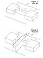
- the FinFETis constructed from a silicon body that includes a source region 12 , a drain region 14 and a fin-shaped channel region 16 .
- the source 12 , drain 14 and channel 16 regionsare formed of a monolithic silicon body that is patterned from a silicon layer provided on a dielectric substrate 18 .
- a gate oxideis grown or deposited over the silicon body, and then a conductive gate 20 as shown in FIG. 1 b is patterned so as to surround the channel region 16 .
- FIG. 2shows a view of a cross-section of the gate and channel region of the FinFET of FIG. 1 b taken at line A-A′.
- the gate 20 and channel region 16are separated by the gate oxide 22 , and the gate 20 surrounds the channel region 16 on both of its sidewalls, thus serving as a double gate that imparts gate voltage to both sides of the channel region 16 .
- the channel width of a FinFETis therefore approximately double the height of the channel region fin, enabling a high driving current compared to semiconductor substrate MOSFETs of comparable size.
- a FinFET bodyis patterned from a layer of silicon germanium (SiGe) that overlies a dielectric layer.
- An epitaxial layer of strained siliconis then formed on the Silicon germanium FinFET body.
- a tensile strainis imparted to the epitaxial silicon as a result of differences in the dimensionalities of a relaxed intrinsic silicon lattice and the silicon germanium crystal lattice that serves as the template on which the epitaxial silicon is grown.
- Strained siliconhas an increased carrier mobility compared to relaxed silicon, and as a result the epitaxial strained silicon provides increased carrier mobility in the FinFET body.
- a higher driving currentcan therefore be realized in a FinFET employing a strained silicon channel layer.
- a silicon on insulator MOSFET devicecomprises a substrate comprising a dielectric layer.
- a FinFET bodyis formed on the dielectric layer.
- the FinFET bodyis typically silicon germanium.
- the FinFET bodyincludes source and drain regions that have a channel region extending therebetween.
- a layer of strained siliconis formed on the surfaces of at least the channel region.
- a gate insulating layeris formed over at least the channel region to cover the strained silicon formed on surfaces of the channel region.
- a conductive gatesurrounds the sidewalls and the top portion of the channel region and is separated from the channel region by the gate insulating layer and the strained silicon.
- a silicon on insulator MOSFET deviceis formed by initially providing a SOI substrate that includes a semiconductor layer overlying a dielectric layer.
- the semiconductor layeris typically silicon germanium.
- the semiconductor layeris patterned to form a FinFET body that includes source and drain regions and a channel region extending therebetween.
- a layer of strained siliconis then formed on the surfaces of at least the channel region.
- a gate insulating layeris formed over at least the strained silicon grown on the channel region to cover the strained silicon grown on the channel region.
- a conductive gateis then formed. The conductive gate surrounds sidewalls and a top portion of the channel region and is separated from the channel region by the gate insulating layer and the strained silicon.
- multiple FinFETs as described abovemay be combined to form CMOS devices, and FinFET bodies may be formed to have multiple channel-regions to thereby provide greater channel width.
- FIG. 1 ashows a body portion of a conventional FinFET
- FIG. 1 bshows a gate portion formed over the body portion of the conventional FinFET of FIG. 1 a;
- FIG. 2shows a cross section of a conventional FinFET gate and channel taken along line A-A′ of FIG. 1 a;
- FIG. 3shows a cross section of a FinFET gate and channel of a FinFET formed in accordance with an embodiment of the present invention
- FIG. 4 ashows a substrate and mask for forming a FinFET in accordance with an embodiment of the invention
- FIG. 4 bshows the structure of FIG. 4 a after etching of the substrate to form a FinFET body
- FIG. 4 cshows the structure of FIG. 4 b after formation of a gate
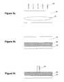
- FIG. 5 ashows the implantation of oxygen into a silicon germanium substrate
- FIG. 5 bshows the structure of FIG. 5 a after annealing to form a buried oxide (BOX) layer of a silicon germanium SOI substrate;
- BOXburied oxide
- FIG. 5 cshows the structure of FIG. 5 b after patterning of a FinFET body from a silicon germanium layer
- FIG. 6 ashows the implantation of hydrogen into a silicon germanium substrate
- FIG. 6 bshows the structure of FIG. 6 a after being inverted and bonded to an oxide layer of a second substrate
- FIG. 6 cshows the structure of FIG. 6 b after annealing to fracture the first substrate in the region of implanted hydrogen
- FIG. 6 dshows the structure of FIG. 6 c after planarization to yield a silicon germanium SOI substrate
- FIG. 7shows a process flow encompassing the preferred embodiment and alternative embodiments.
- FIG. 3A cross section of a gate and a channel region of a FinFET formed in accordance with an embodiment of the present invention is shown in FIG. 3.
- the structurecomprises a silicon germanium channel region 32 on which is grown an epitaxial layer of strained silicon 34 .
- the silicon germanium lattice of the silicon germanium channel region 32is generally more widely spaced than an intrinsic silicon lattice as a result of the presence of the larger germanium atoms in the lattice. Because the atoms of the silicon lattice align with the more widely spread silicon germanium lattice, a tensile strain is created in the silicon layer. The silicon atoms are essentially pulled apart from one another.
- the amount of tensile strain applied to the silicon latticeincreases with the proportion of germanium in the silicon germanium lattice.
- the epitaxial silicon layer 34 grown on the silicon germanium channel region 32is subjected to a tensile strain.
- the application of tensile strain to the silicon latticecauses four of its six silicon valence bands to increase in energy and two of its valence bands to decrease in energy.
- electronseffectively weigh 30 percent less when passing through the lower energy bands of strained silicon.
- the lower energy bandsoffer less resistance to electron flow.
- electronsencounter less vibrational energy from the nucleus of the silicon atom, which causes them to scatter at a rate of 500 to 1000 times less than in relaxed silicon.
- carrier mobilityis dramatically increased in strained silicon as compared to relaxed silicon, offering a potential increase in mobility of 80% or more for electrons and 20% or more for holes.
- the increase in mobilityhas been found to persist for current fields of up to 1.5 megavolts/centimeter.
- a gate insulating layer 36is formed over the strained silicon layer 34 , and a double gate structure 38 is formed around the channel portion 32 overlying the gate insulating layer 36 .
- the structure shown in FIG. 3forms part of a FinFET that exhibits enhanced carrier mobility as the result of the strained silicon layer provided at the surface of the channel region as well as the source and drain regions.
- the aspect ratio of the cross section of the channel portionis probably as high as possible so as to form a tall, narrow channel region that is fully depleted and provides a maximum effective channel width.
- FIG. 4 ashows a SOI substrate including a dielectric layer 40 and a relaxed silicon germanium layer 42 .
- the silicon germanium layer 42preferably has a composition Si 1-x Ge x , where x is approximately 0.2, and is more generally in the range of 0.1-0.3.
- a mask 44is formed on the silicon germanium layer 42 for etching the silicon germanium layer 42 .
- the maskis preferentially a hardmask formed by etching of a bi-layer structure using a photoresist mask of similar shape as an etch mask.
- FIG. 4 bshows the structure of FIG. 4 a after etching using the mask 44 as an etch mask to remove unmasked silicon germanium and to thereby form a silicon germanium FinFET body 46 .
- An epitaxial strained silicon layeris then formed by selective growth on the silicon germanium FinFET body 46 .
- the strained silicon layeris preferably grown by chemical vapor deposition (CVD) using Si 2 H 6 as a source gas with a partial pressure of 30 mPa and a substrate temperature of approximately 600-900 degrees C.
- the epitaxial silicon layeris strained upon its formation as the result of forces within the silicon lattice created as the result of alignment of the silicon atoms through bonding to corresponding atoms of the silicon germanium lattice.
- the epitaxial strained siliconhas a thickness of 100-200 Angstroms.
- a gate insulating layer of silicon oxideis formed over the layer of strained silicon.
- the silicon oxidemay be formed by deposition or may be selectively grown from the strained silicon layer.
- the final thickness of the strained silicon layeris preferably approximately 80-200 A. Therefore, the amount of strained silicon that is initially grown will be determined in part based on whether some of the strained silicon will be consumed during oxide growth.
- a gate 48is formed, yielding the structure illustrated in FIG. 4 c .
- the gateis preferably formed by deposition of a conformal layer of polysilicon over the substrate including the silicon germanium FinFET body 46 , followed by planarization of the polysilicon layer and then patterning using an etch mask to define a gate 48 as shown in FIG. 4 c.
- further processingmay be performed such as formation of insulating spacers on sidewalls of the gate, implantation of dopant in the source and drain regions, formation of source, drain and gate silicides, and formation of a protective layer around the FinFET.
- CMOS FinFETcomplementary metal-oxide-semiconductor
- the source and drain regions of the FinFETmay be connected by multiple channel regions that extend between them, thus providing greater surface area contact between the channel regions and the gate and have greater channel width.
- the silicon germanium SOI substratemay be provided in a variety of manners.
- FIGS. 5 a , 5 b and 5 cshow structures formed using implanted oxygen to form a buried oxide (BOX) layer in a silicon germanium substrate.
- a silicon germanium substrate 50is provided.
- the substratetypically comprises a layer of silicon germanium grown on a silicon wafer.
- Silicon germaniummay be grown, for example, by chemical vapor deposition using disilane (Si 2 H 6 ) and germane (GeH 4 ) as source gases, with a substrate temperature of 600-90 degrees C., a Si 2 H 6 partial pressure of 30 mPa, and a GeH 4 partial pressure of 60 mPa.
- the partial pressure of GeH 4may be gradually increased beginning from a lower pressure or zero pressure to form a gradient composition.
- the thickness of the silicon germanium layermay be determined in accordance with the particular application.
- the portion of the silicon germanium layer to be used for forming the FinFET bodyshould have a uniform composition.
- the silicon germanium substrate 50is implanted with oxygen 52 at an energy sufficient to form an oxygenated region 54 at such a depth to leave a required thickness of silicon germanium above the oxygenated region.
- FIG. 5 bshows the structure of FIG. 5 a after annealing of the silicon germanium substrate 50 to form a buried silicon germanium oxide layer 56 within the substrate. Annealing is typically performed at approximately 1350 degrees C. for approximately four hours, and typically serves to relax any residual strain in the silicon germanium lattice.
- the oxide layer 56serves as the dielectric layer on which monolithic FinFET bodies are later formed, as described above.
- FIG. 5 cshows the structure of FIG. 5 b after patterning a silicon germanium FinFET body 58 (shown in cross section at the channel region) from the silicon germanium layer that overlies the oxide layer 56 .
- FIG. 6 ashows a planarized silicon germanium substrate 60 .
- the substrate 60is implanted with hydrogen 62 to form a hydrogen rich region 64 within the silicon germanium material.
- the hydrogen 62is implanted with an energy such that the amount of silicon germanium remaining above the hydrogen rich region exceeds the thickness of the silicon germanium layer to be formed on the SOI substrate. It may be preferred to implant the hydrogen into a strained region of the silicon germanium
- FIG. 6 bshows the silicon germanium substrate of FIG. 6 a after being cleaned, stripped of oxide in a diluted HF solution, rinsed in deionized water to form an active native oxide on its surface, and then inverted and bonded to a planarized oxide layer 72 formed on a semiconductor layer 74 of second substrate 70 . Bonding may be performed at room temperature, and requires precise planarization of both substrates to provide maximum surface contact for optimal bonding.
- the bonded substratesare annealed, for example at a temperature of 600 degrees C. for approximately three hours. As shown in FIG. 6 c , annealing causes the silicon germanium substrate to fracture along the hydrogen rich region 64 , thus leaving a new substrate comprising a silicon germanium layer 76 bonded to an oxide layer 72 , and having a residual hydrogen rich region 64 at its upper surface.
- the new substrateis subsequently planarized and cleaned, leaving a silicon germanium SOI substrate as shown in FIG. 6 d , from which a silicon germanium FinFET body may be patterned as described previously.
- FIG. 7illustrates a process flow encompassing the preferred embodiment, the aforementioned alternatives and various other alternatives for forming a SOI MOSFET device.
- a SOI substrateis provided ( 80 ).
- the SOI substratecomprises a semiconductor layer that overlies a dielectric layer.
- the semiconductor layeris preferably silicon germanium and the dielectric layer is preferably silicon germanium oxide or silicon oxide.
- the semiconductor layeris then patterned to form a FinFET body comprising source and drain regions having a channel region extending therebetween ( 82 ).
- a layer of strained siliconis then formed on surfaces of at least the channel region ( 84 ), although the layer of strained silicon may additionally be formed over the surfaces of the entire FinFET body.
- a gate insulating layeris formed over at least the strained silicon grown on the channel region of the FinFET body to cover the strained silicon grown on the channel region ( 86 ).
- the gate insulating layermay be an oxide grown from the strained silicon or may be deposited over the strained silicon.
- a conductive gateis then formed ( 88 ). The gate surrounds sidewalls and a top portion of the channel region and is separated from the channel region by the gate insulating layer and the strained silicon layer.
- CMOS devicesdevices having multiple channel regions, and devices employing varying material compositions and material layer structures.
- FinFET structures incorporating strained silicon as described hereinmay also be formed by alternative methods, such as growth of a silicon germanium layer on a semiconductor FinFET body, or implantation of germanium into a silicon FinFET body, followed by growth of strained silicon on the silicon germanium lattice at the surface of the FinFET body.
- the strained siliconmay be formed by implantation of carbon into the surface of a silicon FinFET body. Therefore, strained silicon FinFETs in accordance with the invention may be generally characterized as comprising a layer of strained silicon formed on at least the channel region of a FinFET body.
- the FinFET bodycomprises a layer of silicon germanium at the surface of at least its channel region.
- the strain in a semiconductor layermay be enhanced by implanting germanium into the supporting oxide layer to expand the oxide layer.
- a high k material having a lattice spacing to that of silicon germaniummay be used as the gate insulating layer to provide additional support for the strain in the strained silicon layer.
Landscapes
- Thin Film Transistor (AREA)
- Element Separation (AREA)
Abstract
Description
- 1. Field of the Invention[0001]
- The invention pertains to semiconductor devices, and more particularly to vertical double gate MOSFETs, also known as FinFETs.[0002]
- 2. Related Technology[0003]
- Metal oxide semiconductor field effect transistors (MOSFETs) are the primary component of most semiconductor devices. The conventional MOSFET is constructed from a semiconductor substrate in which dopant-implanted active regions are formed. As a result, the active components of the MOSFET are surrounded by semiconductor material. However, as channel lengths are reduced to less than 100 nm, the use of semiconductor substrate construction in MOSFETs creates performance degrading phenomena such as short channel effect. The short channel effect degrades the ability of the MOSFET gate to control conductivity in the MOSFET channel region due to interactions of the source and drain regions that occur as a result of the semiconductor materials of the semiconductor substrate that surround the active regions.[0004]
- An alternative to the conventional semiconductor substrate construction is silicon on insulator (SOI) construction. In SOI construction, devices such as MOSFETS are formed as monolithic semiconductor structures supported on a dielectric substrate, rather than as regions formed within a semiconductor substrate. SOI devices have been found to have a number of advantages over devices formed using semiconductor substrate construction, such as better isolation between devices, reduced leakage current, reduced latch-up between CMOS elements, reduced chip capacitance, and reduction or elimination of short channel coupling between source and drain regions.[0005]
- One type of MOSFET structure that is formed using SOI construction is conventionally known as a vertical double-gate MOSFET, or a FinFET. As shown in FIG. 1[0006]a, the FinFET is constructed from a silicon body that includes a
source region 12, adrain region 14 and a fin-shaped channel region 16. Thesource 12,drain 14 andchannel 16 regions are formed of a monolithic silicon body that is patterned from a silicon layer provided on adielectric substrate 18. After patterning the silicon body, a gate oxide is grown or deposited over the silicon body, and then aconductive gate 20 as shown in FIG. 1bis patterned so as to surround thechannel region 16. Thegate 20 is patterned from a conductive material such as polysilicon. FIG. 2 shows a view of a cross-section of the gate and channel region of the FinFET of FIG. 1btaken at line A-A′. As seen in FIG. 2, thegate 20 andchannel region 16 are separated by thegate oxide 22, and thegate 20 surrounds thechannel region 16 on both of its sidewalls, thus serving as a double gate that imparts gate voltage to both sides of thechannel region 16. The channel width of a FinFET is therefore approximately double the height of the channel region fin, enabling a high driving current compared to semiconductor substrate MOSFETs of comparable size. - While the conventional FinFET provides the aforementioned advantages over MOSFETs formed on semiconductor substrates due to its SOI construction, some fundamental characteristics of the FinFET such as carrier mobility are the same as those of other MOSFETs because the FinFET source, drain and channel regions are typically made from conventional MOSFET semiconductor materials such as silicon.[0007]
- It is therefore an object of the invention to provide a FinFET device that improves over conventional FinFETs by enhancing characteristics of the device such as carrier mobility.[0008]
- In accordance with embodiments of the invention, a FinFET body is patterned from a layer of silicon germanium (SiGe) that overlies a dielectric layer. An epitaxial layer of strained silicon is then formed on the Silicon germanium FinFET body. A tensile strain is imparted to the epitaxial silicon as a result of differences in the dimensionalities of a relaxed intrinsic silicon lattice and the silicon germanium crystal lattice that serves as the template on which the epitaxial silicon is grown. Strained silicon has an increased carrier mobility compared to relaxed silicon, and as a result the epitaxial strained silicon provides increased carrier mobility in the FinFET body. A higher driving current can therefore be realized in a FinFET employing a strained silicon channel layer.[0009]
- In accordance with one embodiment of the invention, a silicon on insulator MOSFET device comprises a substrate comprising a dielectric layer. A FinFET body is formed on the dielectric layer. The FinFET body is typically silicon germanium. The FinFET body includes source and drain regions that have a channel region extending therebetween. A layer of strained silicon is formed on the surfaces of at least the channel region. A gate insulating layer is formed over at least the channel region to cover the strained silicon formed on surfaces of the channel region. A conductive gate surrounds the sidewalls and the top portion of the channel region and is separated from the channel region by the gate insulating layer and the strained silicon.[0010]
- In accordance with another embodiment of the invention, a silicon on insulator MOSFET device is formed by initially providing a SOI substrate that includes a semiconductor layer overlying a dielectric layer. The semiconductor layer is typically silicon germanium. The semiconductor layer is patterned to form a FinFET body that includes source and drain regions and a channel region extending therebetween. A layer of strained silicon is then formed on the surfaces of at least the channel region. A gate insulating layer is formed over at least the strained silicon grown on the channel region to cover the strained silicon grown on the channel region. A conductive gate is then formed. The conductive gate surrounds sidewalls and a top portion of the channel region and is separated from the channel region by the gate insulating layer and the strained silicon.[0011]
- In accordance with further alternatives, multiple FinFETs as described above may be combined to form CMOS devices, and FinFET bodies may be formed to have multiple channel-regions to thereby provide greater channel width.[0012]
- Embodiments of the invention are described in conjunction with the appended drawings, in which:[0013]
- FIG. 1[0014]ashows a body portion of a conventional FinFET;
- FIG. 1[0015]bshows a gate portion formed over the body portion of the conventional FinFET of FIG. 1a;
- FIG. 2 shows a cross section of a conventional FinFET gate and channel taken along line A-A′ of FIG. 1[0016]a;
- FIG. 3 shows a cross section of a FinFET gate and channel of a FinFET formed in accordance with an embodiment of the present invention;[0017]
- FIG. 4[0018]ashows a substrate and mask for forming a FinFET in accordance with an embodiment of the invention;
- FIG. 4[0019]bshows the structure of FIG. 4aafter etching of the substrate to form a FinFET body;
- FIG. 4[0020]cshows the structure of FIG. 4bafter formation of a gate;
- FIG. 5[0021]ashows the implantation of oxygen into a silicon germanium substrate;
- FIG. 5[0022]bshows the structure of FIG. 5aafter annealing to form a buried oxide (BOX) layer of a silicon germanium SOI substrate;
- FIG. 5[0023]cshows the structure of FIG. 5bafter patterning of a FinFET body from a silicon germanium layer;
- FIG. 6[0024]ashows the implantation of hydrogen into a silicon germanium substrate;
- FIG. 6[0025]bshows the structure of FIG. 6aafter being inverted and bonded to an oxide layer of a second substrate;
- FIG. 6[0026]cshows the structure of FIG. 6bafter annealing to fracture the first substrate in the region of implanted hydrogen;
- FIG. 6[0027]dshows the structure of FIG. 6cafter planarization to yield a silicon germanium SOI substrate;
- FIG. 7 shows a process flow encompassing the preferred embodiment and alternative embodiments.[0028]
- A cross section of a gate and a channel region of a FinFET formed in accordance with an embodiment of the present invention is shown in FIG. 3. As seen in FIG. 3, the structure comprises a silicon[0029]
germanium channel region 32 on which is grown an epitaxial layer ofstrained silicon 34. The silicon germanium lattice of the silicongermanium channel region 32 is generally more widely spaced than an intrinsic silicon lattice as a result of the presence of the larger germanium atoms in the lattice. Because the atoms of the silicon lattice align with the more widely spread silicon germanium lattice, a tensile strain is created in the silicon layer. The silicon atoms are essentially pulled apart from one another. The amount of tensile strain applied to the silicon lattice increases with the proportion of germanium in the silicon germanium lattice. As a result, theepitaxial silicon layer 34 grown on the silicongermanium channel region 32 is subjected to a tensile strain. The application of tensile strain to the silicon lattice causes four of its six silicon valence bands to increase in energy and two of its valence bands to decrease in energy. As a result of quantum effects, electrons effectively weigh 30 percent less when passing through the lower energy bands of strained silicon. Thus the lower energy bands offer less resistance to electron flow. In addition, electrons encounter less vibrational energy from the nucleus of the silicon atom, which causes them to scatter at a rate of 500 to 1000 times less than in relaxed silicon. As a result, carrier mobility is dramatically increased in strained silicon as compared to relaxed silicon, offering a potential increase in mobility of 80% or more for electrons and 20% or more for holes. The increase in mobility has been found to persist for current fields of up to 1.5 megavolts/centimeter. These factors are believed to enable a device speed increase of 35% without further reduction of device size, or a 25% reduction in power consumption without a reduction in performance. - As further shown in FIG. 3, a[0030]
gate insulating layer 36 is formed over thestrained silicon layer 34, and a double gate structure38 is formed around thechannel portion 32 overlying thegate insulating layer 36. - Thus the structure shown in FIG. 3 forms part of a FinFET that exhibits enhanced carrier mobility as the result of the strained silicon layer provided at the surface of the channel region as well as the source and drain regions. The aspect ratio of the cross section of the channel portion is probably as high as possible so as to form a tall, narrow channel region that is fully depleted and provides a maximum effective channel width.[0031]
- A process for forming a FinFET in accordance with a preferred embodiment of the invention is now described with reference to FIGS. 4[0032]a-4c
- FIG. 4[0033]ashows a SOI substrate including a
dielectric layer 40 and a relaxedsilicon germanium layer 42. Various manners for producing such a substrate are discussed below. Thesilicon germanium layer 42 preferably has a composition Si1-xGex, where x is approximately 0.2, and is more generally in the range of 0.1-0.3. - A[0034]
mask 44 is formed on thesilicon germanium layer 42 for etching thesilicon germanium layer 42. The mask is preferentially a hardmask formed by etching of a bi-layer structure using a photoresist mask of similar shape as an etch mask. - FIG. 4[0035]bshows the structure of FIG. 4aafter etching using the
mask 44 as an etch mask to remove unmasked silicon germanium and to thereby form a silicongermanium FinFET body 46. - An epitaxial strained silicon layer is then formed by selective growth on the silicon[0036]
germanium FinFET body 46. The strained silicon layer is preferably grown by chemical vapor deposition (CVD) using Si2H6as a source gas with a partial pressure of 30 mPa and a substrate temperature of approximately 600-900 degrees C. The epitaxial silicon layer is strained upon its formation as the result of forces within the silicon lattice created as the result of alignment of the silicon atoms through bonding to corresponding atoms of the silicon germanium lattice. In preferred embodiments, the epitaxial strained silicon has a thickness of 100-200 Angstroms. - After growth of the strained silicon layer, a gate insulating layer of silicon oxide is formed over the layer of strained silicon. The silicon oxide may be formed by deposition or may be selectively grown from the strained silicon layer. The final thickness of the strained silicon layer is preferably approximately 80-200 A. Therefore, the amount of strained silicon that is initially grown will be determined in part based on whether some of the strained silicon will be consumed during oxide growth.[0037]
- After formation of the gate insulating layer, a[0038]
gate 48 is formed, yielding the structure illustrated in FIG. 4c. The gate is preferably formed by deposition of a conformal layer of polysilicon over the substrate including the silicongermanium FinFET body 46, followed by planarization of the polysilicon layer and then patterning using an etch mask to define agate 48 as shown in FIG. 4c. - Following patterning of the[0039]
gate 48, further processing may be performed such as formation of insulating spacers on sidewalls of the gate, implantation of dopant in the source and drain regions, formation of source, drain and gate silicides, and formation of a protective layer around the FinFET. - While the process described with reference to FIGS. 4[0040]a-4cconcerns the formation of a single FinFET, it should be understood that a variety of alternative structures may be implemented using similar processing. For example, in one alternative implementation, a pair of FinFETs that are doped with respective complementary dopants may have gates that are electrically connected to thereby constitute a CMOS FinFET. In another alternative implementation, the source and drain regions of the FinFET may be connected by multiple channel regions that extend between them, thus providing greater surface area contact between the channel regions and the gate and have greater channel width.
- The silicon germanium SOI substrate may be provided in a variety of manners. FIGS. 5[0041]a,5band5cshow structures formed using implanted oxygen to form a buried oxide (BOX) layer in a silicon germanium substrate. As shown in FIG. 5a, a
silicon germanium substrate 50 is provided. The substrate typically comprises a layer of silicon germanium grown on a silicon wafer. Silicon germanium may be grown, for example, by chemical vapor deposition using disilane (Si2H6) and germane (GeH4) as source gases, with a substrate temperature of 600-90 degrees C., a Si2H6partial pressure of 30 mPa, and a GeH4partial pressure of 60 mPa. Growth of the silicon germanium material may be initiated using these ratios, or alternatively the partial pressure of GeH4may be gradually increased beginning from a lower pressure or zero pressure to form a gradient composition. The thickness of the silicon germanium layer may be determined in accordance with the particular application. Preferably the portion of the silicon germanium layer to be used for forming the FinFET body should have a uniform composition. - As shown in FIG. 5[0042]a, the
silicon germanium substrate 50 is implanted withoxygen 52 at an energy sufficient to form an oxygenatedregion 54 at such a depth to leave a required thickness of silicon germanium above the oxygenated region. - FIG. 5[0043]bshows the structure of FIG. 5aafter annealing of the
silicon germanium substrate 50 to form a buried silicongermanium oxide layer 56 within the substrate. Annealing is typically performed at approximately 1350 degrees C. for approximately four hours, and typically serves to relax any residual strain in the silicon germanium lattice. Theoxide layer 56 serves as the dielectric layer on which monolithic FinFET bodies are later formed, as described above. FIG. 5cshows the structure of FIG. 5bafter patterning a silicon germanium FinFET body58 (shown in cross section at the channel region) from the silicon germanium layer that overlies theoxide layer 56. - FIGS. 6[0044]a-6dshows structures formed in accordance with a second method for forming a silicon germanium SOI substrate. FIG. 6ashows a planarized
silicon germanium substrate 60. Thesubstrate 60 is implanted withhydrogen 62 to form a hydrogenrich region 64 within the silicon germanium material. Thehydrogen 62 is implanted with an energy such that the amount of silicon germanium remaining above the hydrogen rich region exceeds the thickness of the silicon germanium layer to be formed on the SOI substrate. It may be preferred to implant the hydrogen into a strained region of the silicon germanium - FIG. 6[0045]bshows the silicon germanium substrate of FIG. 6aafter being cleaned, stripped of oxide in a diluted HF solution, rinsed in deionized water to form an active native oxide on its surface, and then inverted and bonded to a
planarized oxide layer 72 formed on asemiconductor layer 74 ofsecond substrate 70. Bonding may be performed at room temperature, and requires precise planarization of both substrates to provide maximum surface contact for optimal bonding. - After bonding, the bonded substrates are annealed, for example at a temperature of 600 degrees C. for approximately three hours. As shown in FIG. 6[0046]c, annealing causes the silicon germanium substrate to fracture along the hydrogen
rich region 64, thus leaving a new substrate comprising asilicon germanium layer 76 bonded to anoxide layer 72, and having a residual hydrogenrich region 64 at its upper surface. - The new substrate is subsequently planarized and cleaned, leaving a silicon germanium SOI substrate as shown in FIG. 6[0047]d, from which a silicon germanium FinFET body may be patterned as described previously.
- FIG. 7 illustrates a process flow encompassing the preferred embodiment, the aforementioned alternatives and various other alternatives for forming a SOI MOSFET device. Initially a SOI substrate is provided ([0048]80). The SOI substrate comprises a semiconductor layer that overlies a dielectric layer. The semiconductor layer is preferably silicon germanium and the dielectric layer is preferably silicon germanium oxide or silicon oxide. The semiconductor layer is then patterned to form a FinFET body comprising source and drain regions having a channel region extending therebetween (82). A layer of strained silicon is then formed on surfaces of at least the channel region (84), although the layer of strained silicon may additionally be formed over the surfaces of the entire FinFET body. A gate insulating layer is formed over at least the strained silicon grown on the channel region of the FinFET body to cover the strained silicon grown on the channel region (86). The gate insulating layer may be an oxide grown from the strained silicon or may be deposited over the strained silicon. A conductive gate is then formed (88). The gate surrounds sidewalls and a top portion of the channel region and is separated from the channel region by the gate insulating layer and the strained silicon layer. As mentioned above, a variety of structural implementations may be formed using this process flow, including the single device shown in FIGS. 4a-4c, as well as CMOS devices, devices having multiple channel regions, and devices employing varying material compositions and material layer structures.
- In addition, FinFET structures incorporating strained silicon as described herein may also be formed by alternative methods, such as growth of a silicon germanium layer on a semiconductor FinFET body, or implantation of germanium into a silicon FinFET body, followed by growth of strained silicon on the silicon germanium lattice at the surface of the FinFET body. Further, the strained silicon may be formed by implantation of carbon into the surface of a silicon FinFET body. Therefore, strained silicon FinFETs in accordance with the invention may be generally characterized as comprising a layer of strained silicon formed on at least the channel region of a FinFET body. Typically the FinFET body comprises a layer of silicon germanium at the surface of at least its channel region.[0049]
- In further alternatives, the strain in a semiconductor layer may be enhanced by implanting germanium into the supporting oxide layer to expand the oxide layer. In other alternatives, a high k material having a lattice spacing to that of silicon germanium may be used as the gate insulating layer to provide additional support for the strain in the strained silicon layer.[0050]
- It will be apparent to those having ordinary skill in the art that the tasks described in the above processes are not necessarily exclusive of other tasks, but rather that further tasks may be incorporated into the above processes in accordance with the particular structures to be formed. For example, intermediate processing tasks such as formation and removal of passivation layers or protective layers between processing tasks, formation and removal of photoresist masks and other masking layers, doping and counter-doping, cleaning, planarization, and other tasks, may be performed along with the tasks specifically described above. Further, the process need not be performed on an entire substrate such as an entire wafer, but rather may be performed selectively on sections of the substrate. Thus, while the embodiments illustrated in the figures and described above are presently preferred, it should be understood that these embodiments are offered by way of example only. The invention is not limited to a particular embodiment, but extends to various modifications, combinations, and permutations that fall within the scope of the claimed inventions and their equivalents.[0051]
Claims (27)
1. A silicon on insulator (SOI) MOSFET device comprising:
a substrate comprising a dielectric layer;
a FinFET body formed on the dielectric layer, the FinFET body comprising source and drain regions having a channel region extending therebetween;
a layer of strained silicon formed on surfaces of at least the channel region of the FinFET body;
a gate insulating layer formed over at least the channel region to cover the strained silicon formed on surfaces of the channel region; and
a conductive gate that surrounds sidewalls and a top portion of the channel region and that is separated from the channel region by the gate insulating layer and the strained silicon layer.
2. The device claimed inclaim 1 , wherein the FinFET body has silicon germanium at at least a surface of the channel region.
3. The device claimed inclaim 2 , wherein the silicon germanium FinFET body has a composition Si1-xGexwhere x is in the range of 0.1 to 0.3.
4. The device claimed inclaim 3 , wherein x is approximately 0.2.
4. The device claimed inclaim 1 , wherein the FinFET body comprises at least first and second channel regions extending between the source and drain regions.
6. The device claimed inclaim 1 , wherein the FinFET body is silicon germanium.
7. The device claimed inclaim 1 , wherein the FinFET body comprises a first FinFET body, and wherein the device further comprises:
a second FinFET body formed on the dielectric layer, the second FinFET body comprising second source and drain regions having a second channel region extending therebetween;
a layer of strained silicon formed on surfaces of the second channel region;
a gate insulating layer formed over at least the second channel region to cover the strained silicon formed on surfaces of the second channel region; and
a second conductive gate that surrounds sidewalls and a top portion of the second channel region and that is separated from the second channel region by the gate insulating layer and the strained silicon layer, and that is electrically connected to the conductive gate surrounding the channel region of the first FinFET body,
the source and drain of the first FinFET body being doped with a first dopant, and the source and drain of the second FinFET body being doped with a second dopant complementary to the first dopant.
8. The device claimed inclaim 1 , wherein the gate insulating layer comprises a silicon oxide grown from the strained silicon layer.
9. The device claimed inclaim 1 , wherein the strained silicon layer covers the source and drain regions of the FinFET body.
10. The device claimed inclaim 1 , further comprising a spacer formed on sidewalls of the conductive gate.
11. The device claimed inclaim 1 , wherein the dielectric layer comprises a silicon germanium oxide.
12. A method for forming a silicon on insulator (SOI) MOSFET device comprising:
providing a SOI substrate comprising a semiconductor layer overlying a dielectric layer;
patterning the semiconductor layer to form a FinFET body comprising source and drain regions having a channel region extending therebetween;
forming a layer of strained silicon on surfaces of at least the channel region;
forming a gate insulating layer over at least the strained silicon grown on the channel region to cover the strained silicon grown on the channel region; and
forming a conductive gate that surrounds sidewalls and a top portion of the channel region and is separated from the channel region by the gate insulating layer and the strained silicon.
13. The method claimed inclaim 12 , wherein the FinFET body has silicon germanium at at least a surface of the channel region.
14. The method claimed inclaim 13 , wherein the silicon germanium FinFET body has a composition Si1-xGexwhere x is in the range of 0.1 to 0.3.
15. The method claimed inclaim 14 , wherein x is approximately 0.2.
16. The method claimed inclaim 12 , wherein the semiconductor layer is silicon germanium and the FinFET body is silicon germanium.
17. The method claimed inclaim 12 , wherein forming the conductive gate comprises:
forming a conductive layer over the gate insulating layer and the FinFET body; and
patterning the conductive layer to form the conductive gate.
18. The method claimed inclaim 12 , further comprising implanting the source and drain regions of the FinFET body with a dopant.
19. The method claimed inclaim 12 , wherein the FinFET body comprises a first FinFET body, and wherein the method further comprises:
patterning the semiconductor layer to form a second FinFET body comprising second source and drain regions having a second channel region extending therebetween, concurrently with patterning of said first FinFET body;
forming a layer of strained silicon on surfaces of at least the second channel region of the second FinFET body, concurrently with growing a layer of strained silicon on said first FinFET body;
forming a gate insulating layer over at least the strained silicon grown on the second channel region of said second FinFET body to cover the strained silicon grown on the second channel region, concurrently with forming a gate insulating layer over said first FinFET body; and
forming a second conductive gate that surrounds sidewalls and a top portion of the second channel region and is separated from the second channel region by the gate insulating layer and the strained silicon, concurrently with forming the conductive gate over the first FinFET body,
wherein the conductive gate of the first FinFET body and the conductive gate of the second FinFET are electrically connected.
20. The method claimed inclaim 12 , wherein the FinFET body has at least first and second channel regions extending between the source and drain regions.
21. The method claimed inclaim 12 , wherein the gate insulating layer is a silicon oxide-grown from the strained-silicon layer.
22. The method claimed inclaim 12 , wherein the strained silicon layer covers the source and drain regions of the FinFET body.
23. The method claimed inclaim 12 , further comprising forming a spacer on sidewalls of the conductive gate.
24. The method claimed inclaim 12 , wherein the dielectric layer comprises a silicon germanium oxide.
25. The method claimed inclaim 12 , wherein providing a SOI substrate comprising a silicon germanium layer overlying a dielectric layer comprises:
providing a substrate comprising a silicon germanium layer;
implanting oxygen into the silicon germanium layer; and
annealing the substrate to form a buried silicon germanium oxide layer in the silicon germanium layer.
26. The method claimed inclaim 12 , wherein providing a SOI substrate comprising a silicon germanium layer overlying a dielectric layer comprises:
providing a first substrate comprising a silicon germanium layer;
implanting hydrogen into the silicon germanium layer to form a hydrogen rich region in the silicon germanium layer;
bonding the first substrate to an oxide layer of a second semiconductor substrate;
annealing the bonded first and second substrates to fracture the first substrate in the hydrogen rich region; and
removing the first substrate to yield the second substrate having a silicon germanium layer bonded to said oxide layer.
27. The method claimed inclaim 26 , further comprising planarizing the silicon germanium layer to remove any remaining portion of the hydrogen rich region.
Priority Applications (9)
| Application Number | Priority Date | Filing Date | Title |
|---|---|---|---|
| US10/335,474US6800910B2 (en) | 2002-09-30 | 2002-12-31 | FinFET device incorporating strained silicon in the channel region |
| PCT/US2003/028660WO2004032246A1 (en) | 2002-09-30 | 2003-09-12 | Finfet having improved carrier mobility and method of its formation |
| AU2003266149AAU2003266149A1 (en) | 2002-09-30 | 2003-09-12 | Finfet having improved carrier mobility and method of its formation |
| CNB038232502ACN100524827C (en) | 2002-09-30 | 2003-09-12 | Normal bigri FET having improved carrier mobility and method of its formation |
| JP2004541537AJP2006501672A (en) | 2002-09-30 | 2003-09-12 | FinFET with improved carrier mobility and method of forming the same |
| DE60335391TDE60335391D1 (en) | 2002-09-30 | 2003-09-12 | FINFET WITH IMPROVED CARRIER MOBILITY AND METHOD FOR ITS TRAINING |
| KR1020057005284AKR101020811B1 (en) | 2002-09-30 | 2003-09-12 | FINEFT with improved carrier mobility and method of forming the same |
| EP03799284AEP1547156B1 (en) | 2002-09-30 | 2003-09-12 | Finfet having improved carrier mobility and method of its formation |
| TW092126057ATWI364095B (en) | 2002-09-30 | 2003-09-22 | Finfet having improved carrier mobility and method of its formation |
Applications Claiming Priority (2)
| Application Number | Priority Date | Filing Date | Title |
|---|---|---|---|
| US41522602P | 2002-09-30 | 2002-09-30 | |
| US10/335,474US6800910B2 (en) | 2002-09-30 | 2002-12-31 | FinFET device incorporating strained silicon in the channel region |
Publications (2)
| Publication Number | Publication Date |
|---|---|
| US20040061178A1true US20040061178A1 (en) | 2004-04-01 |
| US6800910B2 US6800910B2 (en) | 2004-10-05 |
Family
ID=32033323
Family Applications (1)
| Application Number | Title | Priority Date | Filing Date |
|---|---|---|---|
| US10/335,474Expired - LifetimeUS6800910B2 (en) | 2002-09-30 | 2002-12-31 | FinFET device incorporating strained silicon in the channel region |
Country Status (9)
| Country | Link |
|---|---|
| US (1) | US6800910B2 (en) |
| EP (1) | EP1547156B1 (en) |
| JP (1) | JP2006501672A (en) |
| KR (1) | KR101020811B1 (en) |
| CN (1) | CN100524827C (en) |
| AU (1) | AU2003266149A1 (en) |
| DE (1) | DE60335391D1 (en) |
| TW (1) | TWI364095B (en) |
| WO (1) | WO2004032246A1 (en) |
Cited By (58)
| Publication number | Priority date | Publication date | Assignee | Title |
|---|---|---|---|---|
| US20030201458A1 (en)* | 2002-03-19 | 2003-10-30 | Clark William F. | Strained fin fets structure and method |
| US20040094807A1 (en)* | 2002-08-23 | 2004-05-20 | Chau Robert S. | Tri-gate devices and methods of fabrication |
| US20040099903A1 (en)* | 2002-11-26 | 2004-05-27 | Taiwan Semiconductor Manufacturing Co., Ltd. | Strained-channel multiple-gate transistor |
| US20040217433A1 (en)* | 2003-04-29 | 2004-11-04 | Yee-Chia Yeo | Doping of semiconductor fin devices |
| US20040266077A1 (en)* | 2003-06-27 | 2004-12-30 | Yee-Chia Yeo | Structure and method for forming the gate electrode in a multiple-gate transistor |
| US20050023633A1 (en)* | 2003-08-01 | 2005-02-03 | Yee-Chia Yeo | Semiconductor-on-insulator SRAM configured using partially-depleted and fully-depleted transistors |
| US20050082522A1 (en)* | 2003-07-25 | 2005-04-21 | Yi-Chun Huang | Strained channel transistor formation |
| US20050121706A1 (en)* | 2003-02-20 | 2005-06-09 | Hao-Yu Chen | Semiconductor nano-rod devices |
| US20050263795A1 (en)* | 2004-05-25 | 2005-12-01 | Jeong-Dong Choi | Semiconductor device having a channel layer and method of manufacturing the same |
| US20050275010A1 (en)* | 2004-06-10 | 2005-12-15 | Hung-Wei Chen | Semiconductor nano-wire devices and methods of fabrication |
| US20060033095A1 (en)* | 2004-08-10 | 2006-02-16 | Doyle Brian S | Non-planar pMOS structure with a strained channel region and an integrated strained CMOS flow |
| US20060076625A1 (en)* | 2004-09-25 | 2006-04-13 | Lee Sung-Young | Field effect transistors having a strained silicon channel and methods of fabricating same |
| US20060084247A1 (en)* | 2004-10-20 | 2006-04-20 | Kaiping Liu | Transistors, integrated circuits, systems, and processes of manufacture with improved work function modulation |
| US20060113522A1 (en)* | 2003-06-23 | 2006-06-01 | Sharp Laboratories Of America, Inc. | Strained silicon fin structure |
| US20060157687A1 (en)* | 2005-01-18 | 2006-07-20 | Doyle Brian S | Non-planar MOS structure with a strained channel region |
| US20060197129A1 (en)* | 2005-03-03 | 2006-09-07 | Triquint Semiconductor, Inc. | Buried and bulk channel finFET and method of making the same |
| US20060202266A1 (en)* | 2005-03-14 | 2006-09-14 | Marko Radosavljevic | Field effect transistor with metal source/drain regions |
| US20060261411A1 (en)* | 2003-06-27 | 2006-11-23 | Hareland Scott A | Nonplanar device with stress incorporation layer and method of fabrication |
| US20060275988A1 (en)* | 2005-06-03 | 2006-12-07 | Atsushi Yagishita | Semiconductor device and method of fabricating the same |
| US20060286755A1 (en)* | 2005-06-15 | 2006-12-21 | Brask Justin K | Method for fabricating transistor with thinned channel |
| US20070001173A1 (en)* | 2005-06-21 | 2007-01-04 | Brask Justin K | Semiconductor device structures and methods of forming semiconductor structures |
| US20070152266A1 (en)* | 2005-12-29 | 2007-07-05 | Intel Corporation | Method and structure for reducing the external resistance of a three-dimensional transistor through use of epitaxial layers |
| US20070238273A1 (en)* | 2006-03-31 | 2007-10-11 | Doyle Brian S | Method of ion implanting for tri-gate devices |
| US20070264762A1 (en)* | 2003-11-04 | 2007-11-15 | Yee-Chia Yeo | Semiconductor-on-insulator SRAM configured using partially-depleted and fully-depleted transistors |
| CN100367505C (en)* | 2004-06-11 | 2008-02-06 | 国际商业机器公司 | Backgate FinFET SRAM |
| US20080157225A1 (en)* | 2006-12-29 | 2008-07-03 | Suman Datta | SRAM and logic transistors with variable height multi-gate transistor architecture |
| US20080164535A1 (en)* | 2007-01-09 | 2008-07-10 | Dureseti Chidambarrao | Curved finfets |
| US20080242010A1 (en)* | 2004-01-17 | 2008-10-02 | Hwa-Sung Rhee | At least penta-sided-channel type of finfet transistor |
| CN100431118C (en)* | 2004-08-05 | 2008-11-05 | 国际商业机器公司 | Three-mask approach constituting the final hardmask for etching the silicon fins of FINFETs |
| US7456476B2 (en) | 2003-06-27 | 2008-11-25 | Intel Corporation | Nonplanar semiconductor device with partially or fully wrapped around gate electrode and methods of fabrication |
| US7479421B2 (en) | 2005-09-28 | 2009-01-20 | Intel Corporation | Process for integrating planar and non-planar CMOS transistors on a bulk substrate and article made thereby |
| CN100459160C (en)* | 2005-02-18 | 2009-02-04 | 富士通微电子株式会社 | Semiconductor device |
| US20090072316A1 (en)* | 2007-09-14 | 2009-03-19 | Advanced Micro Devices, Inc. | Double layer stress for multiple gate transistors |
| US20090149531A1 (en)* | 2007-12-11 | 2009-06-11 | Apoteknos Para La Piel, S.L. | Chemical composition derived from p-hydroxyphenyl propionic acid for the treatment of psoriasis |
| US20090149012A1 (en)* | 2004-09-30 | 2009-06-11 | Brask Justin K | Method of forming a nonplanar transistor with sidewall spacers |
| US20100081227A1 (en)* | 2007-07-03 | 2010-04-01 | Hong Kl-Ha | Luminous device and method of manufacturing the same |
| US7736956B2 (en) | 2005-08-17 | 2010-06-15 | Intel Corporation | Lateral undercut of metal gate in SOI device |
| US7781771B2 (en) | 2004-03-31 | 2010-08-24 | Intel Corporation | Bulk non-planar transistor having strained enhanced mobility and methods of fabrication |
| US7898041B2 (en) | 2005-06-30 | 2011-03-01 | Intel Corporation | Block contact architectures for nanoscale channel transistors |
| US7902014B2 (en) | 2005-09-28 | 2011-03-08 | Intel Corporation | CMOS devices with a single work function gate electrode and method of fabrication |
| US20110147711A1 (en)* | 2009-12-23 | 2011-06-23 | Ravi Pillarisetty | Non-planar germanium quantum well devices |
| US7989280B2 (en) | 2005-11-30 | 2011-08-02 | Intel Corporation | Dielectric interface for group III-V semiconductor device |
| US8067818B2 (en) | 2004-10-25 | 2011-11-29 | Intel Corporation | Nonplanar device with thinned lower body portion and method of fabrication |
| US8084818B2 (en) | 2004-06-30 | 2011-12-27 | Intel Corporation | High mobility tri-gate devices and methods of fabrication |
| US20120091538A1 (en)* | 2010-10-13 | 2012-04-19 | Taiwan Semiconductor Manufacturing Company, Ltd. | Finfet and method of fabricating the same |
| US8183646B2 (en) | 2005-02-23 | 2012-05-22 | Intel Corporation | Field effect transistor with narrow bandgap source and drain regions and method of fabrication |
| US8268709B2 (en) | 2004-09-29 | 2012-09-18 | Intel Corporation | Independently accessed double-gate and tri-gate transistors in same process flow |
| US8362566B2 (en) | 2008-06-23 | 2013-01-29 | Intel Corporation | Stress in trigate devices using complimentary gate fill materials |
| US8617945B2 (en) | 2006-08-02 | 2013-12-31 | Intel Corporation | Stacking fault and twin blocking barrier for integrating III-V on Si |
| US20140312432A1 (en)* | 2012-08-24 | 2014-10-23 | Taiwan Semiconductor Manufacturing Company Limited | Semiconductor arrangement with substrate isolation |
| JP2014220522A (en)* | 2003-03-17 | 2014-11-20 | 三星電子株式会社Samsung Electronics Co.,Ltd. | Semiconductor element |
| CN104183488A (en)* | 2013-05-21 | 2014-12-03 | 中芯国际集成电路制造(上海)有限公司 | FinFET semiconductor device and manufacturing method thereof |
| US20150041810A1 (en)* | 2011-08-30 | 2015-02-12 | Sandia Corporation | Method to fabricate micro and nano diamond devices |
| WO2015047342A1 (en)* | 2013-09-27 | 2015-04-02 | Intel Corporation | Ge and iii-v channel semiconductor devices having maximized compliance and free surface relaxation |
| CN105529241A (en)* | 2014-09-29 | 2016-04-27 | 中芯国际集成电路制造(上海)有限公司 | Semiconductor structure and formation method thereof |
| CN105612622A (en)* | 2013-09-27 | 2016-05-25 | 英特尔公司 | Forming LED structures on silicon fins |
| US9496259B2 (en)* | 2015-04-14 | 2016-11-15 | Taiwan Semiconductor Manufacturing Co., Ltd. | FinFET semiconductor device having fins with stronger structural strength |
| DE112012004134B4 (en)* | 2011-10-27 | 2017-09-07 | International Business Machines Corporation | Method for manufacturing a transistor unit |
Families Citing this family (108)
| Publication number | Priority date | Publication date | Assignee | Title |
|---|---|---|---|---|
| US7074623B2 (en) | 2002-06-07 | 2006-07-11 | Amberwave Systems Corporation | Methods of forming strained-semiconductor-on-insulator finFET device structures |
| US7091068B1 (en)* | 2002-12-06 | 2006-08-15 | Advanced Micro Devices, Inc. | Planarizing sacrificial oxide to improve gate critical dimension in semiconductor devices |
| US6803631B2 (en)* | 2003-01-23 | 2004-10-12 | Advanced Micro Devices, Inc. | Strained channel finfet |
| WO2004073044A2 (en)* | 2003-02-13 | 2004-08-26 | Massachusetts Institute Of Technology | Finfet device and method to make same |
| TWI231994B (en)* | 2003-04-04 | 2005-05-01 | Univ Nat Taiwan | Strained Si FinFET |
| US6909186B2 (en)* | 2003-05-01 | 2005-06-21 | International Business Machines Corporation | High performance FET devices and methods therefor |
| CN1799146A (en)* | 2003-05-30 | 2006-07-05 | 松下电器产业株式会社 | Semiconductor device and method for manufacturing same |
| US6943405B2 (en)* | 2003-07-01 | 2005-09-13 | International Business Machines Corporation | Integrated circuit having pairs of parallel complementary FinFETs |
| EP1519421A1 (en) | 2003-09-25 | 2005-03-30 | Interuniversitair Microelektronica Centrum Vzw | Multiple gate semiconductor device and method for forming same |
| US6921982B2 (en)* | 2003-07-21 | 2005-07-26 | International Business Machines Corporation | FET channel having a strained lattice structure along multiple surfaces |
| EP1503424A3 (en)* | 2003-07-25 | 2008-06-04 | Interuniversitair Micro-Elektronica Centrum (IMEC) | Multiple gate semiconductor device and method for forming same |
| JP2005051241A (en)* | 2003-07-25 | 2005-02-24 | Interuniv Micro Electronica Centrum Vzw | Multilayer gate semiconductor device and manufacturing method thereof |
| US7355253B2 (en)* | 2003-08-22 | 2008-04-08 | International Business Machines Corporation | Strained-channel Fin field effect transistor (FET) with a uniform channel thickness and separate gates |
| US6970373B2 (en)* | 2003-10-02 | 2005-11-29 | Intel Corporation | Method and apparatus for improving stability of a 6T CMOS SRAM cell |
| US6855588B1 (en)* | 2003-10-07 | 2005-02-15 | United Microelectronics Corp. | Method of fabricating a double gate MOSFET device |
| KR100605497B1 (en)* | 2003-11-27 | 2006-07-28 | 삼성전자주식회사 | Methods of manufacturing SOHI substrates, methods of manufacturing semiconductor devices using the same, and semiconductor devices manufactured thereby |
| US6924178B2 (en)* | 2003-12-08 | 2005-08-02 | International Business Machines Corporation | Oxide/nitride stacked in FinFET spacer process |
| US7388258B2 (en)* | 2003-12-10 | 2008-06-17 | International Business Machines Corporation | Sectional field effect devices |
| US7105390B2 (en) | 2003-12-30 | 2006-09-12 | Intel Corporation | Nonplanar transistors with metal gate electrodes |
| US7247912B2 (en)* | 2004-01-05 | 2007-07-24 | International Business Machines Corporation | Structures and methods for making strained MOSFETs |
| US7705345B2 (en)* | 2004-01-07 | 2010-04-27 | International Business Machines Corporation | High performance strained silicon FinFETs device and method for forming same |
| US6936516B1 (en)* | 2004-01-12 | 2005-08-30 | Advanced Micro Devices, Inc. | Replacement gate strained silicon finFET process |
| KR100781538B1 (en)* | 2004-02-07 | 2007-12-03 | 삼성전자주식회사 | Method for manufacturing active structure for improved multi-gate transistor, active structure and multi-gate transistor manufactured thereby |
| US7579280B2 (en) | 2004-06-01 | 2009-08-25 | Intel Corporation | Method of patterning a film |
| DE102005045078B4 (en)* | 2004-09-25 | 2009-01-22 | Samsung Electronics Co., Ltd., Suwon | Field effect transistor with a strained channel layer on sidewalls of a structure on a semiconductor substrate |
| US7332439B2 (en) | 2004-09-29 | 2008-02-19 | Intel Corporation | Metal gate transistors with epitaxial source and drain regions |
| KR100652381B1 (en)* | 2004-10-28 | 2006-12-01 | 삼성전자주식회사 | Multi-Bridge Channel Field Effect Transistor with Numerous Nanowire Channels and Manufacturing Method Thereof |
| CN100392859C (en)* | 2004-11-03 | 2008-06-04 | 中国科学院微电子研究所 | Structure and preparation method of a fish ridge field effect transistor |
| JP2006135067A (en)* | 2004-11-05 | 2006-05-25 | Toshiba Corp | Semiconductor device and manufacturing method thereof |
| US20060113603A1 (en)* | 2004-12-01 | 2006-06-01 | Amberwave Systems Corporation | Hybrid semiconductor-on-insulator structures and related methods |
| US7393733B2 (en) | 2004-12-01 | 2008-07-01 | Amberwave Systems Corporation | Methods of forming hybrid fin field-effect transistor structures |
| KR100630723B1 (en)* | 2004-12-06 | 2006-10-02 | 삼성전자주식회사 | Semiconductor device with multiple crosslinking channel and manufacturing method |
| JP4924419B2 (en) | 2005-02-18 | 2012-04-25 | 富士通セミコンダクター株式会社 | Storage element matrix and semiconductor circuit device using the storage element matrix |
| JP4367357B2 (en)* | 2005-02-28 | 2009-11-18 | セイコーエプソン株式会社 | Manufacturing method of semiconductor device |
| US9153645B2 (en) | 2005-05-17 | 2015-10-06 | Taiwan Semiconductor Manufacturing Company, Ltd. | Lattice-mismatched semiconductor structures with reduced dislocation defect densities and related methods for device fabrication |
| US8324660B2 (en) | 2005-05-17 | 2012-12-04 | Taiwan Semiconductor Manufacturing Company, Ltd. | Lattice-mismatched semiconductor structures with reduced dislocation defect densities and related methods for device fabrication |
| US8110863B2 (en) | 2005-06-01 | 2012-02-07 | Sandisk 3D Llc | TFT charge storage memory cell having high-mobility corrugated channel |
| US7859065B2 (en)* | 2005-06-07 | 2010-12-28 | Nec Corporation | Fin-type field effect transistor and semiconductor device |
| US7902598B2 (en) | 2005-06-24 | 2011-03-08 | Micron Technology, Inc. | Two-sided surround access transistor for a 4.5F2 DRAM cell |
| US7375394B2 (en)* | 2005-07-06 | 2008-05-20 | Applied Intellectual Properties Co., Ltd. | Fringing field induced localized charge trapping memory |
| US7696567B2 (en) | 2005-08-31 | 2010-04-13 | Micron Technology, Inc | Semiconductor memory device |
| US7400031B2 (en)* | 2005-09-19 | 2008-07-15 | International Business Machines Corporation | Asymmetrically stressed CMOS FinFET |
| US7947546B2 (en)* | 2005-10-31 | 2011-05-24 | Chartered Semiconductor Manufacturing, Ltd. | Implant damage control by in-situ C doping during SiGe epitaxy for device applications |
| US7348638B2 (en)* | 2005-11-14 | 2008-03-25 | International Business Machines Corporation | Rotational shear stress for charge carrier mobility modification |
| US7402856B2 (en)* | 2005-12-09 | 2008-07-22 | Intel Corporation | Non-planar microelectronic device having isolation element to mitigate fringe effects and method to fabricate same |
| US7439588B2 (en)* | 2005-12-13 | 2008-10-21 | Intel Corporation | Tri-gate integration with embedded floating body memory cell using a high-K dual metal gate |
| US7512017B2 (en)* | 2005-12-21 | 2009-03-31 | Intel Corporation | Integration of planar and tri-gate devices on the same substrate |
| US7525160B2 (en) | 2005-12-27 | 2009-04-28 | Intel Corporation | Multigate device with recessed strain regions |
| US7396711B2 (en) | 2005-12-27 | 2008-07-08 | Intel Corporation | Method of fabricating a multi-cornered film |
| US20070148926A1 (en)* | 2005-12-28 | 2007-06-28 | Intel Corporation | Dual halo implant for improving short channel effect in three-dimensional tri-gate transistors |
| KR100719180B1 (en)* | 2006-02-28 | 2007-05-17 | 주식회사 하이닉스반도체 | A memory device having a saddle type transistor and a pin type transistor at the same time and a manufacturing method |
| WO2007112066A2 (en) | 2006-03-24 | 2007-10-04 | Amberwave Systems Corporation | Lattice-mismatched semiconductor structures and related methods for device fabrication |
| US20070235763A1 (en)* | 2006-03-29 | 2007-10-11 | Doyle Brian S | Substrate band gap engineered multi-gate pMOS devices |
| US7407847B2 (en)* | 2006-03-31 | 2008-08-05 | Intel Corporation | Stacked multi-gate transistor design and method of fabrication |
| US7425500B2 (en) | 2006-03-31 | 2008-09-16 | Intel Corporation | Uniform silicide metal on epitaxially grown source and drain regions of three-dimensional transistors |
| JP4552908B2 (en)* | 2006-07-26 | 2010-09-29 | エルピーダメモリ株式会社 | Manufacturing method of semiconductor device |
| US8173551B2 (en) | 2006-09-07 | 2012-05-08 | Taiwan Semiconductor Manufacturing Co., Ltd. | Defect reduction using aspect ratio trapping |
| US7435683B2 (en)* | 2006-09-15 | 2008-10-14 | Intel Corporation | Apparatus and method for selectively recessing spacers on multi-gate devices |
| US20080097346A1 (en)* | 2006-09-19 | 2008-04-24 | Alcon, Inc. | Trocar cannula |
| US7700470B2 (en) | 2006-09-22 | 2010-04-20 | Intel Corporation | Selective anisotropic wet etching of workfunction metal for semiconductor devices |
| WO2008039495A1 (en) | 2006-09-27 | 2008-04-03 | Amberwave Systems Corporation | Tri-gate field-effect transistors formed by aspect ratio trapping |
| WO2008039534A2 (en) | 2006-09-27 | 2008-04-03 | Amberwave Systems Corporation | Quantum tunneling devices and circuits with lattice- mismatched semiconductor structures |
| CN100539153C (en)* | 2006-10-02 | 2009-09-09 | 台湾积体电路制造股份有限公司 | Semiconductor structure and memory cell |
| US8502263B2 (en) | 2006-10-19 | 2013-08-06 | Taiwan Semiconductor Manufacturing Company, Ltd. | Light-emitter-based devices with lattice-mismatched semiconductor structures |
| US8368144B2 (en) | 2006-12-18 | 2013-02-05 | Infineon Technologies Ag | Isolated multigate FET circuit blocks with different ground potentials |
| US20080173942A1 (en)* | 2007-01-22 | 2008-07-24 | International Business Machines Corporation | STRUCTURE AND METHOD OF MANUFACTURING A STRAINED FinFET WITH STRESSED SILICIDE |
| DE102007008562A1 (en)* | 2007-02-21 | 2008-08-28 | Qimonda Ag | Field effect transistor arrangement |
| US7821061B2 (en) | 2007-03-29 | 2010-10-26 | Intel Corporation | Silicon germanium and germanium multigate and nanowire structures for logic and multilevel memory applications |
| US7825328B2 (en) | 2007-04-09 | 2010-11-02 | Taiwan Semiconductor Manufacturing Company, Ltd. | Nitride-based multi-junction solar cell modules and methods for making the same |
| US8237151B2 (en) | 2009-01-09 | 2012-08-07 | Taiwan Semiconductor Manufacturing Company, Ltd. | Diode-based devices and methods for making the same |
| US8304805B2 (en) | 2009-01-09 | 2012-11-06 | Taiwan Semiconductor Manufacturing Company, Ltd. | Semiconductor diodes fabricated by aspect ratio trapping with coalesced films |
| WO2008124154A2 (en) | 2007-04-09 | 2008-10-16 | Amberwave Systems Corporation | Photovoltaics on silicon |
| US8329541B2 (en) | 2007-06-15 | 2012-12-11 | Taiwan Semiconductor Manufacturing Company, Ltd. | InP-based transistor fabrication |
| JP2010538495A (en) | 2007-09-07 | 2010-12-09 | アンバーウェーブ・システムズ・コーポレーション | Multi-junction solar cell |
| US8288756B2 (en) | 2007-11-30 | 2012-10-16 | Advanced Micro Devices, Inc. | Hetero-structured, inverted-T field effect transistor |
| US8183667B2 (en) | 2008-06-03 | 2012-05-22 | Taiwan Semiconductor Manufacturing Co., Ltd. | Epitaxial growth of crystalline material |
| US8274097B2 (en) | 2008-07-01 | 2012-09-25 | Taiwan Semiconductor Manufacturing Company, Ltd. | Reduction of edge effects from aspect ratio trapping |
| US8981427B2 (en) | 2008-07-15 | 2015-03-17 | Taiwan Semiconductor Manufacturing Company, Ltd. | Polishing of small composite semiconductor materials |
| EP2335273A4 (en) | 2008-09-19 | 2012-01-25 | Taiwan Semiconductor Mfg | FORMATION OF DEVICES BY GROWTH OF EPITAXIAL LAYERS |
| US20100072515A1 (en) | 2008-09-19 | 2010-03-25 | Amberwave Systems Corporation | Fabrication and structures of crystalline material |
| US8253211B2 (en) | 2008-09-24 | 2012-08-28 | Taiwan Semiconductor Manufacturing Company, Ltd. | Semiconductor sensor structures with reduced dislocation defect densities |
| US20100155801A1 (en)* | 2008-12-22 | 2010-06-24 | Doyle Brian S | Integrated circuit, 1T-1C embedded memory cell containing same, and method of manufacturing 1T-1C memory cell for embedded memory application |
| US7999298B2 (en)* | 2008-12-30 | 2011-08-16 | Intel Corporation | Embedded memory cell and method of manufacturing same |
| US8629446B2 (en) | 2009-04-02 | 2014-01-14 | Taiwan Semiconductor Manufacturing Company, Ltd. | Devices formed from a non-polar plane of a crystalline material and method of making the same |
| US8796759B2 (en) | 2010-07-15 | 2014-08-05 | Taiwan Semiconductor Manufacturing Company, Ltd. | Fin-like field effect transistor (FinFET) device and method of manufacturing same |
| EP2477216A1 (en)* | 2011-01-13 | 2012-07-18 | Soitec | Hybrid bulk/SOI device with a buried doped layer and manufacturing method thereof |
| CN103137671B (en)* | 2011-12-02 | 2015-06-24 | 中芯国际集成电路制造(上海)有限公司 | Multi-grid field effect transistor and manufacturing method thereof |
| US8796695B2 (en) | 2012-06-22 | 2014-08-05 | United Microelectronics Corp. | Multi-gate field-effect transistor and process thereof |
| CN103219384B (en)* | 2013-04-03 | 2015-05-20 | 北京大学 | Anti-single particle radiation multi-grid device and preparation method thereof |
| US9000498B2 (en)* | 2013-06-28 | 2015-04-07 | Stmicroelectronics, Inc. | FinFET with multiple concentration percentages |
| KR101462430B1 (en)* | 2013-07-18 | 2014-11-18 | 경북대학교 산학협력단 | Manufacturing methode of semiconductor device |
| CN105493251A (en)* | 2013-09-27 | 2016-04-13 | 英特尔公司 | Non-planar semiconductor device with multi-layer flexible substrate |
| US9391171B2 (en) | 2014-01-24 | 2016-07-12 | International Business Machines Corporation | Fin field effect transistor including a strained epitaxial semiconductor shell |
| CN104022152B (en)* | 2014-06-04 | 2017-03-01 | 重庆大学 | Double grid p-channel MOSFET with compressive strain thin film strain source and preparation method |
| US9178068B1 (en) | 2014-06-05 | 2015-11-03 | International Business Machines Corporation | FinFET with oxidation-induced stress |
| CN105280496B (en) | 2014-06-05 | 2019-06-11 | 联华电子股份有限公司 | Semiconductor element with fin structure and manufacturing method thereof |
| US9502565B2 (en) | 2014-06-27 | 2016-11-22 | Taiwan Semiconductor Manufacturing Company, Ltd. | Channel strain control for nonplanar compound semiconductor devices |
| US9941406B2 (en) | 2014-08-05 | 2018-04-10 | Taiwan Semiconductor Manufacturing Company, Ltd. | FinFETs with source/drain cladding |
| US9306067B2 (en) | 2014-08-05 | 2016-04-05 | Taiwan Semiconductor Manufacturing Company, Ltd. | Nonplanar device and strain-generating channel dielectric |
| KR102255174B1 (en) | 2014-10-10 | 2021-05-24 | 삼성전자주식회사 | Semiconductor device having active region and method of forming the same |
| US9577101B2 (en) | 2015-03-13 | 2017-02-21 | Taiwan Semiconductor Manufacturing Company, Ltd. | Source/drain regions for fin field effect transistors and methods of forming same |
| US9583626B2 (en) | 2015-04-29 | 2017-02-28 | International Business Machines Corporation | Silicon germanium alloy fins with reduced defects |
| US10079302B2 (en) | 2015-12-28 | 2018-09-18 | International Business Machines Corporation | Silicon germanium fin immune to epitaxy defect |
| FR3053834B1 (en) | 2016-07-05 | 2020-06-12 | Stmicroelectronics Sa | TRANSISTOR STRUCTURE |
| CN109920846B (en)* | 2019-03-11 | 2023-11-03 | 长江存储科技有限责任公司 | Transistor and method of forming same, memory |
| KR102796255B1 (en) | 2020-04-22 | 2025-04-17 | 삼성디스플레이 주식회사 | Display apparatus |
| CN111509048A (en)* | 2020-04-28 | 2020-08-07 | 上海华力集成电路制造有限公司 | N-type fin transistor and its manufacturing method |
| KR20250125638A (en)* | 2024-02-15 | 2025-08-22 | 주식회사 웨이버사시스템즈 | Integrated circuit wafers, integrated circuit boards, and integrated circuit electronic acceleration devices |
Citations (5)
| Publication number | Priority date | Publication date | Assignee | Title |
|---|---|---|---|---|
| US6413802B1 (en)* | 2000-10-23 | 2002-07-02 | The Regents Of The University Of California | Finfet transistor structures having a double gate channel extending vertically from a substrate and methods of manufacture |
| US6475869B1 (en)* | 2001-02-26 | 2002-11-05 | Advanced Micro Devices, Inc. | Method of forming a double gate transistor having an epitaxial silicon/germanium channel region |
| US6562665B1 (en)* | 2000-10-16 | 2003-05-13 | Advanced Micro Devices, Inc. | Fabrication of a field effect transistor with a recess in a semiconductor pillar in SOI technology |
| US6611029B1 (en)* | 2002-11-08 | 2003-08-26 | Advanced Micro Devices, Inc. | Double gate semiconductor device having separate gates |
| US6635909B2 (en)* | 2002-03-19 | 2003-10-21 | International Business Machines Corporation | Strained fin FETs structure and method |
Family Cites Families (5)
| Publication number | Priority date | Publication date | Assignee | Title |
|---|---|---|---|---|
| FR2681472B1 (en)* | 1991-09-18 | 1993-10-29 | Commissariat Energie Atomique | PROCESS FOR PRODUCING THIN FILMS OF SEMICONDUCTOR MATERIAL. |
| US5461250A (en)* | 1992-08-10 | 1995-10-24 | International Business Machines Corporation | SiGe thin film or SOI MOSFET and method for making the same |
| JP2002043576A (en)* | 2000-07-24 | 2002-02-08 | Univ Tohoku | Semiconductor device |
| US7163864B1 (en)* | 2000-10-18 | 2007-01-16 | International Business Machines Corporation | Method of fabricating semiconductor side wall fin |
| JP3782021B2 (en)* | 2002-02-22 | 2006-06-07 | 株式会社東芝 | Semiconductor device, semiconductor device manufacturing method, and semiconductor substrate manufacturing method |
- 2002
- 2002-12-31USUS10/335,474patent/US6800910B2/ennot_activeExpired - Lifetime
- 2003
- 2003-09-12CNCNB038232502Apatent/CN100524827C/ennot_activeExpired - Lifetime
- 2003-09-12JPJP2004541537Apatent/JP2006501672A/enactivePending
- 2003-09-12WOPCT/US2003/028660patent/WO2004032246A1/enactiveApplication Filing
- 2003-09-12EPEP03799284Apatent/EP1547156B1/ennot_activeExpired - Lifetime
- 2003-09-12AUAU2003266149Apatent/AU2003266149A1/ennot_activeAbandoned
- 2003-09-12KRKR1020057005284Apatent/KR101020811B1/ennot_activeExpired - Lifetime
- 2003-09-12DEDE60335391Tpatent/DE60335391D1/ennot_activeExpired - Lifetime
- 2003-09-22TWTW092126057Apatent/TWI364095B/ennot_activeIP Right Cessation
Patent Citations (5)
| Publication number | Priority date | Publication date | Assignee | Title |
|---|---|---|---|---|
| US6562665B1 (en)* | 2000-10-16 | 2003-05-13 | Advanced Micro Devices, Inc. | Fabrication of a field effect transistor with a recess in a semiconductor pillar in SOI technology |
| US6413802B1 (en)* | 2000-10-23 | 2002-07-02 | The Regents Of The University Of California | Finfet transistor structures having a double gate channel extending vertically from a substrate and methods of manufacture |
| US6475869B1 (en)* | 2001-02-26 | 2002-11-05 | Advanced Micro Devices, Inc. | Method of forming a double gate transistor having an epitaxial silicon/germanium channel region |
| US6635909B2 (en)* | 2002-03-19 | 2003-10-21 | International Business Machines Corporation | Strained fin FETs structure and method |
| US6611029B1 (en)* | 2002-11-08 | 2003-08-26 | Advanced Micro Devices, Inc. | Double gate semiconductor device having separate gates |
Cited By (151)
| Publication number | Priority date | Publication date | Assignee | Title |
|---|---|---|---|---|
| US20030201458A1 (en)* | 2002-03-19 | 2003-10-30 | Clark William F. | Strained fin fets structure and method |
| US6849884B2 (en)* | 2002-03-19 | 2005-02-01 | International Business Machines Corporation | Strained Fin FETs structure and method |
| US20040094807A1 (en)* | 2002-08-23 | 2004-05-20 | Chau Robert S. | Tri-gate devices and methods of fabrication |
| US7358121B2 (en) | 2002-08-23 | 2008-04-15 | Intel Corporation | Tri-gate devices and methods of fabrication |
| US7504678B2 (en) | 2002-08-23 | 2009-03-17 | Intel Corporation | Tri-gate devices and methods of fabrication |
| US7560756B2 (en) | 2002-08-23 | 2009-07-14 | Intel Corporation | Tri-gate devices and methods of fabrication |
| US20070034972A1 (en)* | 2002-08-23 | 2007-02-15 | Chau Robert S | Tri-gate devices and methods of fabrication |
| US20040099903A1 (en)* | 2002-11-26 | 2004-05-27 | Taiwan Semiconductor Manufacturing Co., Ltd. | Strained-channel multiple-gate transistor |
| US6855990B2 (en)* | 2002-11-26 | 2005-02-15 | Taiwan Semiconductor Manufacturing Co., Ltd | Strained-channel multiple-gate transistor |
| US20050121706A1 (en)* | 2003-02-20 | 2005-06-09 | Hao-Yu Chen | Semiconductor nano-rod devices |
| JP2014220522A (en)* | 2003-03-17 | 2014-11-20 | 三星電子株式会社Samsung Electronics Co.,Ltd. | Semiconductor element |
| US8790970B2 (en) | 2003-04-29 | 2014-07-29 | Taiwan Semiconductor Manufacturing Company, Ltd. | Doping of semiconductor fin devices |
| US7701008B2 (en) | 2003-04-29 | 2010-04-20 | Taiwan Semiconductor Manufacturing Company, Ltd. | Doping of semiconductor fin devices |
| US20100176424A1 (en)* | 2003-04-29 | 2010-07-15 | Taiwan Semiconductor Manufacturing Company, Ltd. | Doping of Semiconductor Fin Devices |
| US20060234431A1 (en)* | 2003-04-29 | 2006-10-19 | Yee-Chia Yeo | Doping of semiconductor fin devices |
| US8053839B2 (en) | 2003-04-29 | 2011-11-08 | Taiwan Semiconductor Manufacturing Company, Ltd. | Doping of semiconductor fin devices |
| US20060220133A1 (en)* | 2003-04-29 | 2006-10-05 | Yee-Chia Yeo | Doping of semiconductor fin devices |
| US7074656B2 (en) | 2003-04-29 | 2006-07-11 | Taiwan Semiconductor Manufacturing Company, Ltd. | Doping of semiconductor fin devices |
| US20040217433A1 (en)* | 2003-04-29 | 2004-11-04 | Yee-Chia Yeo | Doping of semiconductor fin devices |
| US20060113522A1 (en)* | 2003-06-23 | 2006-06-01 | Sharp Laboratories Of America, Inc. | Strained silicon fin structure |
| US7115945B2 (en)* | 2003-06-23 | 2006-10-03 | Sharp Laboratories Of America, Inc. | Strained silicon fin structure |
| US20110020987A1 (en)* | 2003-06-27 | 2011-01-27 | Hareland Scott A | Nonplanar semiconductor device with partially or fully wrapped around gate electrode and methods of fabrication |
| US7714397B2 (en) | 2003-06-27 | 2010-05-11 | Intel Corporation | Tri-gate transistor device with stress incorporation layer and method of fabrication |
| US7456476B2 (en) | 2003-06-27 | 2008-11-25 | Intel Corporation | Nonplanar semiconductor device with partially or fully wrapped around gate electrode and methods of fabrication |
| US20040266077A1 (en)* | 2003-06-27 | 2004-12-30 | Yee-Chia Yeo | Structure and method for forming the gate electrode in a multiple-gate transistor |
| US20060091428A1 (en)* | 2003-06-27 | 2006-05-04 | Yee-Chia Yeo | Structure and method for forming the gate electrode in a multiple-gate transistor |
| US8273626B2 (en) | 2003-06-27 | 2012-09-25 | Intel Corporationn | Nonplanar semiconductor device with partially or fully wrapped around gate electrode and methods of fabrication |
| US20060261411A1 (en)* | 2003-06-27 | 2006-11-23 | Hareland Scott A | Nonplanar device with stress incorporation layer and method of fabrication |
| US7005330B2 (en) | 2003-06-27 | 2006-02-28 | Taiwan Semiconductor Manufacturing Company, Ltd. | Structure and method for forming the gate electrode in a multiple-gate transistor |
| US7276763B2 (en) | 2003-06-27 | 2007-10-02 | Taiwan Semiconductor Manufacturing Company, Ltd. | Structure and method for forming the gate electrode in a multiple-gate transistor |
| US7820513B2 (en) | 2003-06-27 | 2010-10-26 | Intel Corporation | Nonplanar semiconductor device with partially or fully wrapped around gate electrode and methods of fabrication |
| US8405164B2 (en) | 2003-06-27 | 2013-03-26 | Intel Corporation | Tri-gate transistor device with stress incorporation layer and method of fabrication |
| US20050082522A1 (en)* | 2003-07-25 | 2005-04-21 | Yi-Chun Huang | Strained channel transistor formation |
| US7867860B2 (en) | 2003-07-25 | 2011-01-11 | Taiwan Semiconductor Manufacturing Company, Ltd. | Strained channel transistor formation |
| US20050023633A1 (en)* | 2003-08-01 | 2005-02-03 | Yee-Chia Yeo | Semiconductor-on-insulator SRAM configured using partially-depleted and fully-depleted transistors |
| US7301206B2 (en) | 2003-08-01 | 2007-11-27 | Taiwan Semiconductor Manufacturing Company, Ltd. | Semiconductor-on-insulator SRAM configured using partially-depleted and fully-depleted transistors |
| US7888201B2 (en) | 2003-11-04 | 2011-02-15 | Taiwan Semiconductor Manufacturing Company, Ltd. | Semiconductor-on-insulator SRAM configured using partially-depleted and fully-depleted transistors |
| US20070264762A1 (en)* | 2003-11-04 | 2007-11-15 | Yee-Chia Yeo | Semiconductor-on-insulator SRAM configured using partially-depleted and fully-depleted transistors |
| US7723193B2 (en)* | 2004-01-17 | 2010-05-25 | Samsung Electronics Co., Ltd. | Method of forming an at least penta-sided-channel type of FinFET transistor |
| US20080242010A1 (en)* | 2004-01-17 | 2008-10-02 | Hwa-Sung Rhee | At least penta-sided-channel type of finfet transistor |
| US7781771B2 (en) | 2004-03-31 | 2010-08-24 | Intel Corporation | Bulk non-planar transistor having strained enhanced mobility and methods of fabrication |
| US20050263795A1 (en)* | 2004-05-25 | 2005-12-01 | Jeong-Dong Choi | Semiconductor device having a channel layer and method of manufacturing the same |
| US20050275010A1 (en)* | 2004-06-10 | 2005-12-15 | Hung-Wei Chen | Semiconductor nano-wire devices and methods of fabrication |
| CN100428446C (en)* | 2004-06-10 | 2008-10-22 | 台湾积体电路制造股份有限公司 | Semiconductor element and manufacturing method thereof |
| US7452778B2 (en) | 2004-06-10 | 2008-11-18 | Taiwan Semiconductor Manufacturing Company, Ltd. | Semiconductor nano-wire devices and methods of fabrication |
| CN100367505C (en)* | 2004-06-11 | 2008-02-06 | 国际商业机器公司 | Backgate FinFET SRAM |
| US8084818B2 (en) | 2004-06-30 | 2011-12-27 | Intel Corporation | High mobility tri-gate devices and methods of fabrication |
| CN100431118C (en)* | 2004-08-05 | 2008-11-05 | 国际商业机器公司 | Three-mask approach constituting the final hardmask for etching the silicon fins of FINFETs |
| US20060033095A1 (en)* | 2004-08-10 | 2006-02-16 | Doyle Brian S | Non-planar pMOS structure with a strained channel region and an integrated strained CMOS flow |
| US7960794B2 (en) | 2004-08-10 | 2011-06-14 | Intel Corporation | Non-planar pMOS structure with a strained channel region and an integrated strained CMOS flow |
| US7348284B2 (en) | 2004-08-10 | 2008-03-25 | Intel Corporation | Non-planar pMOS structure with a strained channel region and an integrated strained CMOS flow |
| US20060076625A1 (en)* | 2004-09-25 | 2006-04-13 | Lee Sung-Young | Field effect transistors having a strained silicon channel and methods of fabricating same |
| US8268709B2 (en) | 2004-09-29 | 2012-09-18 | Intel Corporation | Independently accessed double-gate and tri-gate transistors in same process flow |
| US8399922B2 (en) | 2004-09-29 | 2013-03-19 | Intel Corporation | Independently accessed double-gate and tri-gate transistors |
| US20090149012A1 (en)* | 2004-09-30 | 2009-06-11 | Brask Justin K | Method of forming a nonplanar transistor with sidewall spacers |
| US7611943B2 (en) | 2004-10-20 | 2009-11-03 | Texas Instruments Incorporated | Transistors, integrated circuits, systems, and processes of manufacture with improved work function modulation |
| US20060084247A1 (en)* | 2004-10-20 | 2006-04-20 | Kaiping Liu | Transistors, integrated circuits, systems, and processes of manufacture with improved work function modulation |
| US8749026B2 (en) | 2004-10-25 | 2014-06-10 | Intel Corporation | Nonplanar device with thinned lower body portion and method of fabrication |
| US8067818B2 (en) | 2004-10-25 | 2011-11-29 | Intel Corporation | Nonplanar device with thinned lower body portion and method of fabrication |
| US9741809B2 (en) | 2004-10-25 | 2017-08-22 | Intel Corporation | Nonplanar device with thinned lower body portion and method of fabrication |
| US8502351B2 (en) | 2004-10-25 | 2013-08-06 | Intel Corporation | Nonplanar device with thinned lower body portion and method of fabrication |
| US10236356B2 (en) | 2004-10-25 | 2019-03-19 | Intel Corporation | Nonplanar device with thinned lower body portion and method of fabrication |
| US9190518B2 (en) | 2004-10-25 | 2015-11-17 | Intel Corporation | Nonplanar device with thinned lower body portion and method of fabrication |
| US7531393B2 (en) | 2005-01-18 | 2009-05-12 | Intel Corporation | Non-planar MOS structure with a strained channel region |
| WO2006078469A1 (en)* | 2005-01-18 | 2006-07-27 | Intel Corporation | Non-planar mos structure with a strained channel region |
| KR100903902B1 (en)* | 2005-01-18 | 2009-06-19 | 인텔 코오퍼레이션 | Non-planar mos structure with a strained channel region |
| DE112006000229B4 (en)* | 2005-01-18 | 2016-04-14 | Intel Corporation | Non-planar MOS structure with a strained channel region and method of fabricating such a structure |
| US7193279B2 (en) | 2005-01-18 | 2007-03-20 | Intel Corporation | Non-planar MOS structure with a strained channel region |
| US20060157687A1 (en)* | 2005-01-18 | 2006-07-20 | Doyle Brian S | Non-planar MOS structure with a strained channel region |
| GB2437867B (en)* | 2005-01-18 | 2008-07-09 | Intel Corp | Non-planer mos structure with a strained channel region |
| US20060157794A1 (en)* | 2005-01-18 | 2006-07-20 | Doyle Brian S | Non-planar MOS structure with a strained channel region |
| GB2437867A (en)* | 2005-01-18 | 2007-11-07 | Intel Corp | Non-planer mos structure with a strained channel region |
| CN100459160C (en)* | 2005-02-18 | 2009-02-04 | 富士通微电子株式会社 | Semiconductor device |
| US9368583B2 (en) | 2005-02-23 | 2016-06-14 | Intel Corporation | Field effect transistor with narrow bandgap source and drain regions and method of fabrication |
| US8183646B2 (en) | 2005-02-23 | 2012-05-22 | Intel Corporation | Field effect transistor with narrow bandgap source and drain regions and method of fabrication |
| US9048314B2 (en) | 2005-02-23 | 2015-06-02 | Intel Corporation | Field effect transistor with narrow bandgap source and drain regions and method of fabrication |
| US10121897B2 (en) | 2005-02-23 | 2018-11-06 | Intel Corporation | Field effect transistor with narrow bandgap source and drain regions and method of fabrication |
| US8816394B2 (en) | 2005-02-23 | 2014-08-26 | Intel Corporation | Field effect transistor with narrow bandgap source and drain regions and method of fabrication |
| US8664694B2 (en) | 2005-02-23 | 2014-03-04 | Intel Corporation | Field effect transistor with narrow bandgap source and drain regions and method of fabrication |
| US9748391B2 (en) | 2005-02-23 | 2017-08-29 | Intel Corporation | Field effect transistor with narrow bandgap source and drain regions and method of fabrication |
| US8368135B2 (en) | 2005-02-23 | 2013-02-05 | Intel Corporation | Field effect transistor with narrow bandgap source and drain regions and method of fabrication |
| US9614083B2 (en) | 2005-02-23 | 2017-04-04 | Intel Corporation | Field effect transistor with narrow bandgap source and drain regions and method of fabrication |
| US20060197129A1 (en)* | 2005-03-03 | 2006-09-07 | Triquint Semiconductor, Inc. | Buried and bulk channel finFET and method of making the same |
| US20060202266A1 (en)* | 2005-03-14 | 2006-09-14 | Marko Radosavljevic | Field effect transistor with metal source/drain regions |
| US7879675B2 (en) | 2005-03-14 | 2011-02-01 | Intel Corporation | Field effect transistor with metal source/drain regions |
| US7371644B2 (en)* | 2005-06-03 | 2008-05-13 | Kabushiki Kaisha Toshiba | Semiconductor device and method of fabricating the same |
| US7723171B2 (en) | 2005-06-03 | 2010-05-25 | Kabushiki Kaisha Toshiba | Semiconductor device and method of fabricating the same |
| US20060275988A1 (en)* | 2005-06-03 | 2006-12-07 | Atsushi Yagishita | Semiconductor device and method of fabricating the same |
| US20060286755A1 (en)* | 2005-06-15 | 2006-12-21 | Brask Justin K | Method for fabricating transistor with thinned channel |
| US9806195B2 (en) | 2005-06-15 | 2017-10-31 | Intel Corporation | Method for fabricating transistor with thinned channel |
| US11978799B2 (en) | 2005-06-15 | 2024-05-07 | Tahoe Research, Ltd. | Method for fabricating transistor with thinned channel |
| US7858481B2 (en) | 2005-06-15 | 2010-12-28 | Intel Corporation | Method for fabricating transistor with thinned channel |
| US9337307B2 (en) | 2005-06-15 | 2016-05-10 | Intel Corporation | Method for fabricating transistor with thinned channel |
| US8581258B2 (en) | 2005-06-21 | 2013-11-12 | Intel Corporation | Semiconductor device structures and methods of forming semiconductor structures |
| US7547637B2 (en) | 2005-06-21 | 2009-06-16 | Intel Corporation | Methods for patterning a semiconductor film |
| US8933458B2 (en) | 2005-06-21 | 2015-01-13 | Intel Corporation | Semiconductor device structures and methods of forming semiconductor structures |
| US20070001173A1 (en)* | 2005-06-21 | 2007-01-04 | Brask Justin K | Semiconductor device structures and methods of forming semiconductor structures |
| US9761724B2 (en) | 2005-06-21 | 2017-09-12 | Intel Corporation | Semiconductor device structures and methods of forming semiconductor structures |
| US8071983B2 (en) | 2005-06-21 | 2011-12-06 | Intel Corporation | Semiconductor device structures and methods of forming semiconductor structures |
| US9385180B2 (en) | 2005-06-21 | 2016-07-05 | Intel Corporation | Semiconductor device structures and methods of forming semiconductor structures |
| US7898041B2 (en) | 2005-06-30 | 2011-03-01 | Intel Corporation | Block contact architectures for nanoscale channel transistors |
| US7736956B2 (en) | 2005-08-17 | 2010-06-15 | Intel Corporation | Lateral undercut of metal gate in SOI device |
| US8294180B2 (en) | 2005-09-28 | 2012-10-23 | Intel Corporation | CMOS devices with a single work function gate electrode and method of fabrication |
| US7902014B2 (en) | 2005-09-28 | 2011-03-08 | Intel Corporation | CMOS devices with a single work function gate electrode and method of fabrication |
| US20090090976A1 (en)* | 2005-09-28 | 2009-04-09 | Intel Corporation | Process for integrating planar and non-planar cmos transistors on a bulk substrate and article made thereby |
| US8193567B2 (en) | 2005-09-28 | 2012-06-05 | Intel Corporation | Process for integrating planar and non-planar CMOS transistors on a bulk substrate and article made thereby |
| US7479421B2 (en) | 2005-09-28 | 2009-01-20 | Intel Corporation | Process for integrating planar and non-planar CMOS transistors on a bulk substrate and article made thereby |
| US7989280B2 (en) | 2005-11-30 | 2011-08-02 | Intel Corporation | Dielectric interface for group III-V semiconductor device |
| US20070152266A1 (en)* | 2005-12-29 | 2007-07-05 | Intel Corporation | Method and structure for reducing the external resistance of a three-dimensional transistor through use of epitaxial layers |
| US20070238273A1 (en)* | 2006-03-31 | 2007-10-11 | Doyle Brian S | Method of ion implanting for tri-gate devices |
| US7449373B2 (en) | 2006-03-31 | 2008-11-11 | Intel Corporation | Method of ion implanting for tri-gate devices |
| US8617945B2 (en) | 2006-08-02 | 2013-12-31 | Intel Corporation | Stacking fault and twin blocking barrier for integrating III-V on Si |
| US20080157225A1 (en)* | 2006-12-29 | 2008-07-03 | Suman Datta | SRAM and logic transistors with variable height multi-gate transistor architecture |
| US7538391B2 (en) | 2007-01-09 | 2009-05-26 | International Business Machines Corporation | Curved FINFETs |
| US20080164535A1 (en)* | 2007-01-09 | 2008-07-10 | Dureseti Chidambarrao | Curved finfets |
| US8293554B2 (en)* | 2007-07-03 | 2012-10-23 | Samsung Electronics Co., Ltd. | Luminous device and method of manufacturing the same |
| US20100081227A1 (en)* | 2007-07-03 | 2010-04-01 | Hong Kl-Ha | Luminous device and method of manufacturing the same |
| US20090072316A1 (en)* | 2007-09-14 | 2009-03-19 | Advanced Micro Devices, Inc. | Double layer stress for multiple gate transistors |
| US7671418B2 (en) | 2007-09-14 | 2010-03-02 | Advanced Micro Devices, Inc. | Double layer stress for multiple gate transistors |
| US20090149531A1 (en)* | 2007-12-11 | 2009-06-11 | Apoteknos Para La Piel, S.L. | Chemical composition derived from p-hydroxyphenyl propionic acid for the treatment of psoriasis |
| US9806193B2 (en) | 2008-06-23 | 2017-10-31 | Intel Corporation | Stress in trigate devices using complimentary gate fill materials |
| US8741733B2 (en) | 2008-06-23 | 2014-06-03 | Intel Corporation | Stress in trigate devices using complimentary gate fill materials |
| US9450092B2 (en) | 2008-06-23 | 2016-09-20 | Intel Corporation | Stress in trigate devices using complimentary gate fill materials |
| US9224754B2 (en) | 2008-06-23 | 2015-12-29 | Intel Corporation | Stress in trigate devices using complimentary gate fill materials |
| US8362566B2 (en) | 2008-06-23 | 2013-01-29 | Intel Corporation | Stress in trigate devices using complimentary gate fill materials |
| US9799759B2 (en) | 2009-12-23 | 2017-10-24 | Intel Corporation | Techniques for forming non-planar germanium quantum well devices |
| US20110147711A1 (en)* | 2009-12-23 | 2011-06-23 | Ravi Pillarisetty | Non-planar germanium quantum well devices |
| US8575596B2 (en) | 2009-12-23 | 2013-11-05 | Intel Corporation | Non-planar germanium quantum well devices |
| US10236369B2 (en) | 2009-12-23 | 2019-03-19 | Intel Corporation | Techniques for forming non-planar germanium quantum well devices |
| US9263557B2 (en) | 2009-12-23 | 2016-02-16 | Intel Corporation | Techniques for forming non-planar germanium quantum well devices |
| US9153671B2 (en) | 2009-12-23 | 2015-10-06 | Intel Corporation | Techniques for forming non-planar germanium quantum well devices |
| US8283653B2 (en) | 2009-12-23 | 2012-10-09 | Intel Corporation | Non-planar germanium quantum well devices |
| WO2011087570A1 (en)* | 2009-12-23 | 2011-07-21 | Intel Corporation | Non-planar germanium quantum well devices |
| US20120091538A1 (en)* | 2010-10-13 | 2012-04-19 | Taiwan Semiconductor Manufacturing Company, Ltd. | Finfet and method of fabricating the same |
| US8440517B2 (en)* | 2010-10-13 | 2013-05-14 | Taiwan Semiconductor Manufacturing Company, Ltd. | FinFET and method of fabricating the same |
| US9620596B2 (en)* | 2011-08-30 | 2017-04-11 | Sandia Corporation | Method to fabricate micro and nano diamond devices |
| US20150041810A1 (en)* | 2011-08-30 | 2015-02-12 | Sandia Corporation | Method to fabricate micro and nano diamond devices |
| DE112012004134B4 (en)* | 2011-10-27 | 2017-09-07 | International Business Machines Corporation | Method for manufacturing a transistor unit |
| US9947773B2 (en)* | 2012-08-24 | 2018-04-17 | Taiwan Semiconductor Manufacturing Company, Ltd. | Semiconductor arrangement with substrate isolation |
| US20140312432A1 (en)* | 2012-08-24 | 2014-10-23 | Taiwan Semiconductor Manufacturing Company Limited | Semiconductor arrangement with substrate isolation |
| CN104183488A (en)* | 2013-05-21 | 2014-12-03 | 中芯国际集成电路制造(上海)有限公司 | FinFET semiconductor device and manufacturing method thereof |
| US9570614B2 (en) | 2013-09-27 | 2017-02-14 | Intel Corporation | Ge and III-V channel semiconductor devices having maximized compliance and free surface relaxation |
| US9847448B2 (en)* | 2013-09-27 | 2017-12-19 | Intel Corporation | Forming LED structures on silicon fins |
| US9905651B2 (en) | 2013-09-27 | 2018-02-27 | Intel Corporation | GE and III-V channel semiconductor devices having maximized compliance and free surface relaxation |
| WO2015047342A1 (en)* | 2013-09-27 | 2015-04-02 | Intel Corporation | Ge and iii-v channel semiconductor devices having maximized compliance and free surface relaxation |
| CN105612622A (en)* | 2013-09-27 | 2016-05-25 | 英特尔公司 | Forming LED structures on silicon fins |
| CN110071168A (en)* | 2013-09-27 | 2019-07-30 | 英特尔公司 | Ge and III-V channel semiconductor devices with maximum compliance and free surface relaxation |
| US20160163918A1 (en)* | 2013-09-27 | 2016-06-09 | Intel Corporation | Forming led structures on silicon fins |
| CN105529241A (en)* | 2014-09-29 | 2016-04-27 | 中芯国际集成电路制造(上海)有限公司 | Semiconductor structure and formation method thereof |
| US9859276B2 (en) | 2015-04-14 | 2018-01-02 | Taiwan Semiconductor Manufacturing Co., Ltd. | FinFET semiconductor device having fins with stronger structural strength |
| US9496259B2 (en)* | 2015-04-14 | 2016-11-15 | Taiwan Semiconductor Manufacturing Co., Ltd. | FinFET semiconductor device having fins with stronger structural strength |
Also Published As
| Publication number | Publication date |
|---|---|
| CN100524827C (en) | 2009-08-05 |
| KR101020811B1 (en) | 2011-03-09 |
| TWI364095B (en) | 2012-05-11 |
| DE60335391D1 (en) | 2011-01-27 |
| AU2003266149A1 (en) | 2004-04-23 |
| JP2006501672A (en) | 2006-01-12 |
| EP1547156B1 (en) | 2010-12-15 |
| US6800910B2 (en) | 2004-10-05 |
| EP1547156A1 (en) | 2005-06-29 |
| CN1685523A (en) | 2005-10-19 |
| TW200414452A (en) | 2004-08-01 |
| KR20050047129A (en) | 2005-05-19 |
| WO2004032246A1 (en) | 2004-04-15 |
Similar Documents
| Publication | Publication Date | Title |
|---|---|---|
| US6800910B2 (en) | FinFET device incorporating strained silicon in the channel region | |
| US7701019B2 (en) | Tensile strained substrate | |
| US6852600B1 (en) | Strained silicon MOSFET having silicon source/drain regions and method for its fabrication | |
| US7071065B1 (en) | Strained silicon PMOS having silicon germanium source/drain extensions and method for its fabrication | |
| US7138302B2 (en) | Method of fabricating an integrated circuit channel region | |
| US6943087B1 (en) | Semiconductor on insulator MOSFET having strained silicon channel | |
| TWI352433B (en) | Stressed field effect transistors on hybrid orient | |
| US6929992B1 (en) | Strained silicon MOSFETs having NMOS gates with work functions for compensating NMOS threshold voltage shift | |
| US20050054164A1 (en) | Strained silicon MOSFETs having reduced diffusion of n-type dopants | |
| KR101600553B1 (en) | Methods for fabricating mos devices having epitaxially grown stress-inducing source and drain regions | |
| CN100365766C (en) | Method for forming thick strained silicon layer and semiconductor structure containing thick strained silicon layer | |
| US6849527B1 (en) | Strained silicon MOSFET having improved carrier mobility, strained silicon CMOS device, and methods of their formation | |
| US20100187578A1 (en) | Stress enhanced transistor devices and methods of making | |
| US7033869B1 (en) | Strained silicon semiconductor on insulator MOSFET | |
| KR101093785B1 (en) | Semiconductors on SOI Substrates and Devices Formed therefrom | |
| US20090166761A1 (en) | Field effect transistor structure with an insulating layer at the junction | |
| US7015078B1 (en) | Silicon on insulator substrate having improved thermal conductivity and method of its formation | |
| US20110306170A1 (en) | Novel Method to Improve Performance by Enhancing Poly Gate Doping Concentration in an Embedded SiGe PMOS Process | |
| US6924182B1 (en) | Strained silicon MOSFET having reduced leakage and method of its formation | |
| US6900143B1 (en) | Strained silicon MOSFETs having improved thermal dissipation | |
| US6893929B1 (en) | Method of forming strained silicon MOSFET having improved threshold voltage under the gate ends |
Legal Events
| Date | Code | Title | Description |
|---|---|---|---|
| AS | Assignment | Owner name:ADVANCED MICRO DEVICES INC., CALIFORNIA Free format text:ASSIGNMENT OF ASSIGNORS INTEREST;ASSIGNORS:LIN, MING-REN;GOO, JUNG-SUK;WANG, HAIHONG;AND OTHERS;REEL/FRAME:013638/0276;SIGNING DATES FROM 20020927 TO 20021003 | |
| FEPP | Fee payment procedure | Free format text:PAYOR NUMBER ASSIGNED (ORIGINAL EVENT CODE: ASPN); ENTITY STATUS OF PATENT OWNER: LARGE ENTITY | |
| STCF | Information on status: patent grant | Free format text:PATENTED CASE | |
| FPAY | Fee payment | Year of fee payment:4 | |
| FPAY | Fee payment | Year of fee payment:8 | |
| FPAY | Fee payment | Year of fee payment:12 |