US20040060518A1 - Apparatus for inverted multi-wafer MOCVD fabrication - Google Patents
Apparatus for inverted multi-wafer MOCVD fabricationDownload PDFInfo
- Publication number
- US20040060518A1 US20040060518A1US10/256,814US25681402AUS2004060518A1US 20040060518 A1US20040060518 A1US 20040060518A1US 25681402 AUS25681402 AUS 25681402AUS 2004060518 A1US2004060518 A1US 2004060518A1
- Authority
- US
- United States
- Prior art keywords
- susceptor
- chamber
- reactor
- inlet
- wafers
- Prior art date
- Legal status (The legal status is an assumption and is not a legal conclusion. Google has not performed a legal analysis and makes no representation as to the accuracy of the status listed.)
- Granted
Links
Images


Classifications
- C—CHEMISTRY; METALLURGY
- C23—COATING METALLIC MATERIAL; COATING MATERIAL WITH METALLIC MATERIAL; CHEMICAL SURFACE TREATMENT; DIFFUSION TREATMENT OF METALLIC MATERIAL; COATING BY VACUUM EVAPORATION, BY SPUTTERING, BY ION IMPLANTATION OR BY CHEMICAL VAPOUR DEPOSITION, IN GENERAL; INHIBITING CORROSION OF METALLIC MATERIAL OR INCRUSTATION IN GENERAL
- C23C—COATING METALLIC MATERIAL; COATING MATERIAL WITH METALLIC MATERIAL; SURFACE TREATMENT OF METALLIC MATERIAL BY DIFFUSION INTO THE SURFACE, BY CHEMICAL CONVERSION OR SUBSTITUTION; COATING BY VACUUM EVAPORATION, BY SPUTTERING, BY ION IMPLANTATION OR BY CHEMICAL VAPOUR DEPOSITION, IN GENERAL
- C23C16/00—Chemical coating by decomposition of gaseous compounds, without leaving reaction products of surface material in the coating, i.e. chemical vapour deposition [CVD] processes
- C23C16/44—Chemical coating by decomposition of gaseous compounds, without leaving reaction products of surface material in the coating, i.e. chemical vapour deposition [CVD] processes characterised by the method of coating
- C23C16/455—Chemical coating by decomposition of gaseous compounds, without leaving reaction products of surface material in the coating, i.e. chemical vapour deposition [CVD] processes characterised by the method of coating characterised by the method used for introducing gases into reaction chamber or for modifying gas flows in reaction chamber
- C23C16/45563—Gas nozzles
- C23C16/45565—Shower nozzles
- C—CHEMISTRY; METALLURGY
- C23—COATING METALLIC MATERIAL; COATING MATERIAL WITH METALLIC MATERIAL; CHEMICAL SURFACE TREATMENT; DIFFUSION TREATMENT OF METALLIC MATERIAL; COATING BY VACUUM EVAPORATION, BY SPUTTERING, BY ION IMPLANTATION OR BY CHEMICAL VAPOUR DEPOSITION, IN GENERAL; INHIBITING CORROSION OF METALLIC MATERIAL OR INCRUSTATION IN GENERAL
- C23C—COATING METALLIC MATERIAL; COATING MATERIAL WITH METALLIC MATERIAL; SURFACE TREATMENT OF METALLIC MATERIAL BY DIFFUSION INTO THE SURFACE, BY CHEMICAL CONVERSION OR SUBSTITUTION; COATING BY VACUUM EVAPORATION, BY SPUTTERING, BY ION IMPLANTATION OR BY CHEMICAL VAPOUR DEPOSITION, IN GENERAL
- C23C16/00—Chemical coating by decomposition of gaseous compounds, without leaving reaction products of surface material in the coating, i.e. chemical vapour deposition [CVD] processes
- C23C16/44—Chemical coating by decomposition of gaseous compounds, without leaving reaction products of surface material in the coating, i.e. chemical vapour deposition [CVD] processes characterised by the method of coating
- C23C16/455—Chemical coating by decomposition of gaseous compounds, without leaving reaction products of surface material in the coating, i.e. chemical vapour deposition [CVD] processes characterised by the method of coating characterised by the method used for introducing gases into reaction chamber or for modifying gas flows in reaction chamber
- C23C16/45502—Flow conditions in reaction chamber
- C—CHEMISTRY; METALLURGY
- C23—COATING METALLIC MATERIAL; COATING MATERIAL WITH METALLIC MATERIAL; CHEMICAL SURFACE TREATMENT; DIFFUSION TREATMENT OF METALLIC MATERIAL; COATING BY VACUUM EVAPORATION, BY SPUTTERING, BY ION IMPLANTATION OR BY CHEMICAL VAPOUR DEPOSITION, IN GENERAL; INHIBITING CORROSION OF METALLIC MATERIAL OR INCRUSTATION IN GENERAL
- C23C—COATING METALLIC MATERIAL; COATING MATERIAL WITH METALLIC MATERIAL; SURFACE TREATMENT OF METALLIC MATERIAL BY DIFFUSION INTO THE SURFACE, BY CHEMICAL CONVERSION OR SUBSTITUTION; COATING BY VACUUM EVAPORATION, BY SPUTTERING, BY ION IMPLANTATION OR BY CHEMICAL VAPOUR DEPOSITION, IN GENERAL
- C23C16/00—Chemical coating by decomposition of gaseous compounds, without leaving reaction products of surface material in the coating, i.e. chemical vapour deposition [CVD] processes
- C23C16/44—Chemical coating by decomposition of gaseous compounds, without leaving reaction products of surface material in the coating, i.e. chemical vapour deposition [CVD] processes characterised by the method of coating
- C23C16/458—Chemical coating by decomposition of gaseous compounds, without leaving reaction products of surface material in the coating, i.e. chemical vapour deposition [CVD] processes characterised by the method of coating characterised by the method used for supporting substrates in the reaction chamber
- C23C16/4582—Rigid and flat substrates, e.g. plates or discs
- C23C16/4583—Rigid and flat substrates, e.g. plates or discs the substrate being supported substantially horizontally
- C23C16/4584—Rigid and flat substrates, e.g. plates or discs the substrate being supported substantially horizontally the substrate being rotated
- C—CHEMISTRY; METALLURGY
- C23—COATING METALLIC MATERIAL; COATING MATERIAL WITH METALLIC MATERIAL; CHEMICAL SURFACE TREATMENT; DIFFUSION TREATMENT OF METALLIC MATERIAL; COATING BY VACUUM EVAPORATION, BY SPUTTERING, BY ION IMPLANTATION OR BY CHEMICAL VAPOUR DEPOSITION, IN GENERAL; INHIBITING CORROSION OF METALLIC MATERIAL OR INCRUSTATION IN GENERAL
- C23C—COATING METALLIC MATERIAL; COATING MATERIAL WITH METALLIC MATERIAL; SURFACE TREATMENT OF METALLIC MATERIAL BY DIFFUSION INTO THE SURFACE, BY CHEMICAL CONVERSION OR SUBSTITUTION; COATING BY VACUUM EVAPORATION, BY SPUTTERING, BY ION IMPLANTATION OR BY CHEMICAL VAPOUR DEPOSITION, IN GENERAL
- C23C16/00—Chemical coating by decomposition of gaseous compounds, without leaving reaction products of surface material in the coating, i.e. chemical vapour deposition [CVD] processes
- C23C16/44—Chemical coating by decomposition of gaseous compounds, without leaving reaction products of surface material in the coating, i.e. chemical vapour deposition [CVD] processes characterised by the method of coating
- C23C16/52—Controlling or regulating the coating process
- C—CHEMISTRY; METALLURGY
- C30—CRYSTAL GROWTH
- C30B—SINGLE-CRYSTAL GROWTH; UNIDIRECTIONAL SOLIDIFICATION OF EUTECTIC MATERIAL OR UNIDIRECTIONAL DEMIXING OF EUTECTOID MATERIAL; REFINING BY ZONE-MELTING OF MATERIAL; PRODUCTION OF A HOMOGENEOUS POLYCRYSTALLINE MATERIAL WITH DEFINED STRUCTURE; SINGLE CRYSTALS OR HOMOGENEOUS POLYCRYSTALLINE MATERIAL WITH DEFINED STRUCTURE; AFTER-TREATMENT OF SINGLE CRYSTALS OR A HOMOGENEOUS POLYCRYSTALLINE MATERIAL WITH DEFINED STRUCTURE; APPARATUS THEREFOR
- C30B25/00—Single-crystal growth by chemical reaction of reactive gases, e.g. chemical vapour-deposition growth
- C30B25/02—Epitaxial-layer growth
- C30B25/10—Heating of the reaction chamber or the substrate
- C—CHEMISTRY; METALLURGY
- C30—CRYSTAL GROWTH
- C30B—SINGLE-CRYSTAL GROWTH; UNIDIRECTIONAL SOLIDIFICATION OF EUTECTIC MATERIAL OR UNIDIRECTIONAL DEMIXING OF EUTECTOID MATERIAL; REFINING BY ZONE-MELTING OF MATERIAL; PRODUCTION OF A HOMOGENEOUS POLYCRYSTALLINE MATERIAL WITH DEFINED STRUCTURE; SINGLE CRYSTALS OR HOMOGENEOUS POLYCRYSTALLINE MATERIAL WITH DEFINED STRUCTURE; AFTER-TREATMENT OF SINGLE CRYSTALS OR A HOMOGENEOUS POLYCRYSTALLINE MATERIAL WITH DEFINED STRUCTURE; APPARATUS THEREFOR
- C30B25/00—Single-crystal growth by chemical reaction of reactive gases, e.g. chemical vapour-deposition growth
- C30B25/02—Epitaxial-layer growth
- C30B25/14—Feed and outlet means for the gases; Modifying the flow of the reactive gases
Definitions
- This inventionrelates to fabricating semiconductor devices and more particularly to an apparatus for fabricating semiconductor devices using metalorganic chemical vapor deposition (MOCVD).
- MOCVDmetalorganic chemical vapor deposition
- Group III nitride based semiconductor devicescan be fabricated in MOCVD systems using different material systems, with MOCVD systems more recently being used to fabricate Group III nitride based devices. Growth of Group III nitride based semiconductor devices in MOCVD systems is generally described in DenBaars and Keller, Semiconductors and Semimetals , Vol. 50, Academic Press Inc., 1997, p. 11-35.
- One of the concerns in fabricating Group III nitride devicesis the ability to produce uniform materials with minimal impurities in the device layers, while providing sharp interfaces between layers. Impurities and poor interfaces between layers can negatively impact device performance and can prevent consistent reproduction of semiconductor devices.
- Some conventional multi-wafer MOCVD reactorsutilize a rotatable susceptor that is mounted at the bottom of the reactor chamber. [See Emcore Discover and Enterprise Series of the TurboDisc Tools, provided by Emcore Inc.]. Semiconductor wafers are held on the top surface of the susceptor and a heating element is arranged below the susceptor to heat the susceptor and the wafers. Reactant growth gasses enter the reactor to deposit the desired materials on the wafer with the susceptor rotating to provide a more uniform deposition of the materials on the wafer.
- a large boundary layer over a susceptorcan also limit the susceptor's speed of rotation. As the rotation speed of a heated susceptor is increased, the boundary layer can cause turbulence that adds to the turbulence from the convection forces of the lower temperature growth gasses. This can lead to further non-uniformity in the device layers.
- Another disadvantage of conventional MOCVD reactorsis that the growth gasses that do not deposit on the wafers (or susceptor) can deposit on the sidewalls or top surface of the reactor chamber above the susceptor. These deposits can adversely impact the reactor's ability to grow good quality layers.
- the depositscan react with gasses for subsequent layers and redeposit on the wafers during fabrication.
- the depositscan be introduced as impurities in the subsequent layers and the deposits can reduce the sharpness between layers. This can ultimately limit the reactor's ability to accurately reproduce the semiconductor devices.
- a metal organic vapor phase epitaxy (MOVPE) system for the growth of Group III-V compound semiconductor materialsis described in Aria et al., Highly Uniform Growth on a Low - Pressure MOPVE Multiple Wafer System, Journal of Crystal Growth 170, Pgs. 88-91 (1997).
- the wafersare held in a susceptor and placed facedown (inverted) in the growth chamber, with the flow gasses flowing under the growth surfaces.
- the susceptorrotates, thereby rotating the wafers to attain a more uniform growth.
- Gassesare injected into the chamber from one of the sidewalls of the chamber, through a triple flow channel, and the gas exhaust in on the opposite sidewall.
- Group V species (hydride gasses) and H 2 carrier gas, Group III (organometals) and H 2 carrier gas, and purging gasflow into the reactor through the triple flow channel's upper, middle and lower channels, respectively.
- a chimney reactorhas wafers held on heated susceptors (usually two) that are vertically mounted on the interior side walls of the reactor.
- heated susceptorsusually two
- the intent of the chimney reactor designis to create upward convective gas flow near the susceptor to help promote rapid gas switching for growth of abrupt heterojunctions.
- a cold carrier gas containing reactantsenters at the base of the reactor and flows upward into the heated region.
- One of the disadvantages of this designis that asymmetric flow conditions result in the primary gas flow being located near one side of the reactor and reverse flow near the opposite side. This results in different deposition rates at the two susceptors. Also, with upward gas flow, the growth rate uniformity at the leading edge of the susceptor is much greater than at its trailing edge due to depletion of the reactants.
- the present inventionseeks to provide an improved method and apparatus for the fabrication of semiconductor devices, and in particular the fabrication of semiconductor devices in MOCVD reactors.
- a semiconductor fabrication reactoraccording to the present invention comprises a rotatable susceptor mounted to the top of a reactor chamber.
- One or more wafersare mounted to a surface of the susceptor and the rotation of the susceptor causes the wafers to rotate within the chamber.
- a heaterheats the susceptor and a chamber gas inlet allows semiconductor growth gasses into the reactor chamber to deposit semiconductor material on said wafers.
- the inletis preferably at or below the level of said wafers.
- a chamber gas outletis included to allow growth gasses to exit the chamber.
- the outletis preferably at or above the level of the wafers.
- Another embodiment according to the inventioncomprises a semiconductor fabrication system that includes a source of gasses for forming epitaxial layers on wafers and a source of gasses for dopants in said epitaxial layers.
- a gas linecarries the dopant and epitaxial source gasses to a reactor for growing semiconductor devices on wafers, and the source gasses in the gas line are injected into the reactor through a reactor inlet.
- the reactorcomprises an inverted susceptor mounted in a reactor chamber that is capable of rotating. One or more wafers are mounted to a surface of the susceptor, the rotation of the susceptor causing the wafers to rotate within the chamber.
- a heaterheats the susceptor and the source gasses deposit semiconductor material on the wafers.
- a chamber outletallows the growth gasses to exit the chamber.
- the inlet at or below the level of said wafers and the outletis above the level of said wafers.
- the susceptorhas a face down surface facing the bottom of said chamber, and the wafers are mounted to the face down surface.
- the depth of the boundary layeris reduced, which reduces the turbulence generated when lower temperature growth gasses encounter the boundary layer.
- the growth gassescan also more easily penetrate the boundary layer and the susceptor can be rotated at a higher rotation rate. This arrangement also helps reduce the level of impurities in the semiconductor material that are introduced from deposits within the reactor chamber.
- FIG. 1is a simplified schematic of an embodiment of an MOCVD semiconductor fabrication system according to the present invention
- FIG. 2is a sectional view of one embodiment of a reactor according to the present invention.
- FIG. 3is a sectional view of another embodiment of a reactor according to the present invention having a central rotation rod gas inlet;
- FIG. 4is a below perspective view of an embodiment of a susceptor according to the present invention that can be used in the reactor in FIG. 3;
- FIG. 5is a sectional view of another embodiment of a reactor according to the present invention having a central bottom gas inlet
- FIG. 6is a sectional view of another embodiment of a reactor according to the present invention having bottom showerhead gas inlet;
- FIG. 7is a sectional view of another embodiment of a reactor according to the present invention having sidewall gas inlet.
- FIG. 8is a sectional view of another embodiment of a reactor according to the present invention having a height adjustable susceptor.
- MOCVD reactors with inverted susceptors according to the present inventioncan be used in many different semiconductor fabrication systems, but are particularly adapted for use in MOCVD fabrication systems of the type shown in FIG. 1.
- MOCVDis a nonequilibrium growth technique that relies on vapor transport of precursers and subsequent reactions of Group III alkyls and Group V hydrides in a heated zone. Composition and growth rate are controlled by controlling mass flow rate and dilution of various components of the gas stream to the MOCVD reactor.
- Organometallic Group III growth gas sourcesare either liquids such as trimethylgallium (TMGa) and trimethylaluminum (TMAl), or solids such as trimethylindium (TMIn).
- TMGatrimethylgallium
- TMAltrimethylaluminum
- TMIntrimethylindium
- the organometallic sourcesare stored in bubblers through which a carrier gas (typically hydrogen) flows.
- the bubbler temperaturecontrols the vapor pressure over source material.
- Carrier gaswill saturate with vapor from the organometallic source and transport vapor to the heated substrate.
- Group V growth gas sourcesare most commonly gaseous hydrides, for example NH 3 for nitride growth.
- Dopant materialscan be metal organic precursers [diethylzine (DEZn), cyclopenin dienyl magnesium (Cp 2 Mg)j or hydrides (silane or disilane). Growth gasses and dopants are supplied to the reactor and are deposited as epitaxial layers on a substrate or wafer. One or more wafers are held on a structure of graphite called a susceptor that can be heated by a radio frequency (RF) coil, resistance heated, or radiantly heated by a strip heater, which in turn heats the wafers.
- RFradio frequency
- the MOCVD semiconductor fabrication system 10comprises a reactor chamber 12 having a susceptor 14 that is mounted to the top of the chamber 12 and is inverted.
- the susceptor 14can hold a plurality of wafers 16 that can be made of many different materials such as sapphire, silicon (Si), silicon carbide (SiC), aluminum gallium nitride (AlGaN), gallium arsenide (GaAs).
- Sisilicon
- SiCsilicon carbide
- AlGaNaluminum gallium nitride
- GaAsgallium arsenide
- a preferred waferis made of SiC because it has a much closer crystal lattice match to Group III nitrides compared to other materials, which results in Group III nitride films of higher quality.
- SiCalso has a very high thermal conductivity so that the total output power of Group III nitride devices on SiC is not limited by the thermal dissipation of the wafer.
- the availability of semi insulating SiC wafersalso provides the capacity for device isolation and reduced parasitic capacitance that make commercial devices possible.
- SiC substratesare available from Cree, Inc., of Durham, N.C. and methods for producing them are set forth in the scientific literature as well as in a U.S. Pat. Nos. Re. 34,861; 4,946,547; and 5,200,022.
- the susceptor 14is heated by heater 18 to maintain wafers 16 at a predetermined temperature.
- the temperatureis typically between 400 and 1200 degrees centigrade (° C.), but can be higher or lower depending on the type of growth desired.
- the heater 18can be any of the heating devices listed above, but is usually a radio frequency (RF) or resistance coil.
- a hydrogen or nitrogen carrier gas 20is supplied to a gas line 22 .
- the carrier gas 20is also supplied through mass flow controllers 24 a - c to respective bubblers 26 a - c.
- Bubbler 26 acan have an organometallic Group III source as described above.
- Bubblers 26 b and 26 cmay also contain a similar organometallic compound to be able to grow an alloy of a Group III compound.
- the bubblers 26 a - care typically maintained at a predetermined temperature by constant temperature baths 28 a - c to ensure a constant vapor pressure of the organometallic compound before it is carried to the reactor chamber 12 by the carrier gas 20 .
- the carrier gas 20which passes through bubblers 28 a - c is mixed with the carrier gas 20 flowing within the gas line 22 by opening the desired combination of valves 30 a - c.
- the mixed gasis then introduced into the reactor chamber 12 through a gas inlet port 32 , which can be located at different locations on the reactor, but in the system 10 is located at the bottom of the chamber 12 .
- a nitrogen containing gas 34such as ammonia is supplied to the gas line 22 through a mass flow controller 36 and the flow of nitrogen containing gas is controlled by valve 38 . If the carrier gas 20 is mixed with the nitrogen containing gas 34 , and the organometallic vapor within the gas line 22 is introduced into the reactor chamber 12 , the elements are present to grow gallium nitride on the substrates 16 through thermal decomposition of the molecules in the organometallic and nitrogen containing gas.
- one of the bubblers 26 a - c not being used for the organometallic compoundscan be used for a dopant material.
- Many different doping materialscan be used such as beryllium, calcium, zinc, or carbon, with preferred materials being magnesium (Mg) or silicon (Si).
- Bubbler 26 b or 26 ccan be used for an alloy material such as boron, aluminum, indium, phosphorous, arsenic or other materials.
- the appropriate valve 30 a - cis opened to allow the dopant to flow into gas line 22 with the organometallic and nitrogen containing gas 34 , the growth of the doped layer of gallium nitride can take place on substrates 16 .
- the gas within the reactor chamber 12can be purged through a gas purge line 40 connected to a pump 42 operable under hydraulic pressure. Further, a purge valve 44 allows gas pressure to build up or be bled off from the reactor chamber 12 .
- the growth processis typically stopped by shutting off the organometallic and dopant sources by closing valves 30 a - c, and keeping the nitrogen containing gas 36 and the carrier gas 20 flowing.
- the reactor chamber 12can be purged with a gas 46 that can be controlled through a mass flow controller 48 and valve 50 .
- the purgeis aided by opening valve 44 to allow the pump 42 to evacuate the reaction chamber 12 of excess growth gasses.
- the purge gas 46is hydrogen, but can be other gasses. Turning off power to the heater 18 then cools the substrates 16 .
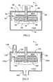
- FIG. 2shows one embodiment of a MOCVD reactor 60 in accordance with the present invention.
- the reactor 60can be used to fabricate many different semiconductor devices from different material systems, but is particularly applicable to fabricating devices from the Group III nitride material system and its alloys, in an MOCVD fabrication system.
- the reactor 60comprises a reactor chamber 62 , with a susceptor 64 that is, inverted and mounted from the reactor's top surface 66 .
- the susceptor 64can be made of many heat conductive materials, with a suitable material being graphite.
- Semiconductor wafers 68are mounted on the susceptor's face down surface 70 that faces the chamber's bottom surface 72 , with typical susceptors capable of holding approximately six three inch wafers and up to eighteen two inch wafers.
- the waferscan be held to the susceptor surface 70 by many different mechanisms including, but not limited to, mounting faceplates, clamps, clips, adhesives, tape, etc.
- the susceptor 64is held within the reactor chamber 60 by a rotation rod 74 that can be rotated so that the susceptor 64 is also rotated.
- the susceptoris heated by a heating element 80 that is arranged between the susceptor 64 and the chamber's top surface.
- the heater 80can be any of the heating devices listed above, but is usually a radio frequency (RF) or resistance coil.
- RFradio frequency
- a hot gas boundary layer 82forms over the susceptor surface 70 and the wafers 68 .
- the growth gassescan enter the chamber 62 in many different ways and through different walls of the chamber 62 .
- the depth of the boundary layer 82is reduced compared to conventional reactor chambers that have a susceptor at the bottom.
- the susceptor 64is heated and generates hot gas, the heated gas rises.
- the boundary layer 82is compressed against the susceptor 64 and wafers 68 by the rising of the hot gas.
- the reduced boundary layer heightreduces the turbulence generated when lower temperature growth gasses encounter the boundary layer 82 , which allows for more uniform deposition of materials on the wafers 68 .
- the growth gassescan also more easily penetrate the boundary layer 82 and as a result, more of the growth gasses deposit on the wafers 68 . This decreases the amount of deposition gasses necessary to form the desired semiconductor device.
- the reduced boundary layeralso reduces gas convection that can occur when the susceptor 64 rotates. As a result, the susceptor 64 can be rotated much faster than conventionally arranged susceptors. In the reactor 10 , the susceptor can be rotated above 100 revolutions per minute (rpm) and up to several thousand rpm.
- the reduced boundary layer 82also allows the deposition gasses to deposit on the wafers 68 under increased reactor chamber pressure to further facilitate efficient fabrication. Depending on the device being fabricated, the pressure can be below 1 ⁇ 8 of an atmosphere to more that 10 atmospheres.
- Another advantage of the inverted susceptor arrangementis that most of the growth gasses that do not deposit on the wafers rise past the susceptor 64 toward the top of the chamber 62 . These gasses can form deposits 84 on the side walls and top surface of the chamber 62 behind the susceptor. These deposits are less likely to interact with subsequent growth gasses to introduce impurities into the material deposited on the wafers 68 because the growth gasses will not encounter these deposits until they are past the wafers. That is, the gasses encounter these impurities when they are past the point when they are depositing reactants on the wafers. Gasses that do not deposit on the wafers or reactor walls can exit the chamber through a top gas outlet, although the outlet could at different locations on the chamber.
- FIG. 3shows an embodiment of an MOCVD reactor 90 in accordance with the present invention that is similar to the reactor 60 in FIG. 2.
- the reactorhas a rotation rod 92 that is hollow so that deposition gasses can enter the reactor chamber 94 through the rotation rod 92 .
- FIG. 4shows a susceptor 96 that can be used in reactor 90 , which includes a central gas inlet 98 that allows gas from the rotation rod 92 to enter the reactor chamber 94 through the susceptor 96 .
- the gasses from the inletare drawn to the susceptor's perimeter and along the way, some of the growth gasses deposit on the wafers 100 . Gasses that do not deposit on the wafers, pass off the edge of the susceptor 96 and are drawn toward the chamber's top surface 102 .
- these gassescan form deposits 106 on the inside of the chamber's sidewalls 108 a, 108 b and inside of the chamber's top surface 102 , that are downstream and behind the susceptor 96 . These deposits are less likely to adversely effect the fabrication of subsequent layers as described above.
- Gassescan exit the reactor chamber 94 through a gas outlet 110 that is preferably at the top of the reactor chamber, which promotes flow of the gasses past the wafers and then to the top of the chamber.
- FIG. 5shows another embodiment of an MOCVD reactor 120 in accordance with the invention, where the growth gasses enter the chamber 122 through a central bottom inlet 124 that is directed toward the wafers 126 on the rotating susceptor 128 .
- the growth gassesrise toward the susceptor 128 where gasses are deposited on the wafers 126 .
- any gasses that do not deposit on the wafers 126are drawn past the susceptor 128 where they can form deposits 130 on the inside of the chamber's sidewalls 132 a, 132 b and inside of the chamber's top surface 134 .
- the reactoralso has a top gas outlet 136 .
- FIG. 6shows another embodiment of an MOCVD reactor 140 in accordance with the present invention, where the growth gasses enter the reactor chamber 142 through a bottom “showerhead” inlet 144 .
- the inlet 144has multiple boreholes 145 for the growth gasses to pass into the chamber where they rise toward the wafers 146 on the rotating susceptor 148 .
- the bore-holes 145 in the inlet 144provide for a more uniform application of the growth gasses across the susceptor 148 , which provides for a more uniform deposition of materials on the wafers 146 .
- the gasses that do not deposit on the wafersare drawn downstream and if they do not deposit on the walls of the reactor chamber 142 , they can exit the chamber through the top outlet 149 .
- FIG. 7shows another embodiment of an MOCVD reactor 150 in accordance with the present invention, where the deposition gasses enter the reactor chamber 152 through a sidewall inlet 154 .
- the gasses that do not deposit on the wafers 156 on the rotating susceptor 158are drawn downstream where they can form deposits 159 on the inside of the reactor's walls.
- the reactorcan also have a top gas outlet 160 , which is arranged so that the gasses pass from the inlet 154 toward the top of the chamber 152 .
- the growth gassesrise toward the susceptor 158 where semiconductor material can be deposited on the wafers 156 .
- FIG. 8shows still another embodiment of an MOCVD reactor 170 in accordance with the present invention, that includes a reactor chamber 171 , rotating susceptor 172 , wafers 174 on the susceptor, and a showerhead gas inlet 175 , all of which are similar those in reactor 140 of FIG. 6.
- the reactor 170operates in the same way as the reactor 140 in FIG. 6.
- the susceptor 172is mounted to the reactor's top surface 176 by a rod 178 that is movable in directions shown be arrows 177 a, 177 b, to adjust the distance between the showerhead inlet 175 and the susceptor 172 .
- This adjustmentcan vary the concentration of reactants in the growth gasses that react with the wafers 174 , to vary the semiconductor growth conditions and rate.
- the susceptor 172can be further adjusted in the direction of arrows 178 a, 178 b to vary the angle between the susceptor 172 and the gas inlet 175 .
- the angle of the gas inlet 175can be adjusted in the direction of arrows 179 a, 179 b to also adjust the angle between the susceptor 172 and the inlet 175 .
- These adjustmentscan also vary the semiconductor grown conditions and rate on the wafers 174 .
- the movable susceptor arrangement and angle adjustable susceptor and inlet arrangementcan also be used in reactors 60 , 120 , 150 , above that have gas inlets through the susceptor, a bottom inlet and a side inlet, respectively.
- the reactorscan include only one or all of these adjustment options.
Landscapes
- Chemical & Material Sciences (AREA)
- Chemical Kinetics & Catalysis (AREA)
- General Chemical & Material Sciences (AREA)
- Engineering & Computer Science (AREA)
- Materials Engineering (AREA)
- Metallurgy (AREA)
- Organic Chemistry (AREA)
- Mechanical Engineering (AREA)
- Crystallography & Structural Chemistry (AREA)
- Chemical Vapour Deposition (AREA)
Abstract
Description
- 1. Field of the Invention[0001]
- This invention relates to fabricating semiconductor devices and more particularly to an apparatus for fabricating semiconductor devices using metalorganic chemical vapor deposition (MOCVD).[0002]
- 2. Description of the Related Art[0003]
- Numerous semiconductor devices can be fabricated in MOCVD systems using different material systems, with MOCVD systems more recently being used to fabricate Group III nitride based devices. Growth of Group III nitride based semiconductor devices in MOCVD systems is generally described in DenBaars and Keller,[0004]Semiconductors and Semimetals, Vol. 50, Academic Press Inc., 1997, p. 11-35. One of the concerns in fabricating Group III nitride devices is the ability to produce uniform materials with minimal impurities in the device layers, while providing sharp interfaces between layers. Impurities and poor interfaces between layers can negatively impact device performance and can prevent consistent reproduction of semiconductor devices.
- Some conventional multi-wafer MOCVD reactors utilize a rotatable susceptor that is mounted at the bottom of the reactor chamber. [See Emcore Discover and Enterprise Series of the TurboDisc Tools, provided by Emcore Inc.]. Semiconductor wafers are held on the top surface of the susceptor and a heating element is arranged below the susceptor to heat the susceptor and the wafers. Reactant growth gasses enter the reactor to deposit the desired materials on the wafer with the susceptor rotating to provide a more uniform deposition of the materials on the wafer.[0005]
- One the disadvantages of these conventional MOCVD reactors is that a large and non-uniform boundary layer thickness of hot air can form over the wafers and susceptor as a result of the heating of the susceptor. During growth, heat from the susceptor causes gasses to rise and the boundary layers can extend to the top surface of the reactor chamber. Reactant growth gasses are injected into the reactor chamber, usually through a top inlet. When the lower temperature growth gasses encounter the hot gasses heat convention can occur, which causes turbulence within the reactor. This turbulence can result in non-uniform deposition of materials on the wafer. It is also difficult for the deposition gasses to diffuse through a larger boundary layer and as a result, much of the growth gasses do not deposit on the wafers. This increases the amount of growth gasses necessary to form the desired semiconductor device.[0006]
- A large boundary layer over a susceptor can also limit the susceptor's speed of rotation. As the rotation speed of a heated susceptor is increased, the boundary layer can cause turbulence that adds to the turbulence from the convection forces of the lower temperature growth gasses. This can lead to further non-uniformity in the device layers.[0007]
- Another disadvantage of conventional MOCVD reactors is that the growth gasses that do not deposit on the wafers (or susceptor) can deposit on the sidewalls or top surface of the reactor chamber above the susceptor. These deposits can adversely impact the reactor's ability to grow good quality layers. The deposits can react with gasses for subsequent layers and redeposit on the wafers during fabrication. The deposits can be introduced as impurities in the subsequent layers and the deposits can reduce the sharpness between layers. This can ultimately limit the reactor's ability to accurately reproduce the semiconductor devices.[0008]
- A metal organic vapor phase epitaxy (MOVPE) system for the growth of Group III-V compound semiconductor materials is described in Aria et al.,[0009]Highly Uniform Growth on a Low-Pressure MOPVE Multiple Wafer System,Journal of Crystal
Growth 170, Pgs. 88-91 (1997). The wafers are held in a susceptor and placed facedown (inverted) in the growth chamber, with the flow gasses flowing under the growth surfaces. The susceptor rotates, thereby rotating the wafers to attain a more uniform growth. Gasses are injected into the chamber from one of the sidewalls of the chamber, through a triple flow channel, and the gas exhaust in on the opposite sidewall. Group V species (hydride gasses) and H2carrier gas, Group III (organometals) and H2carrier gas, and purging gas flow into the reactor through the triple flow channel's upper, middle and lower channels, respectively. - One disadvantage this of system is that because the inlet flow channels are on one chamber side wall and the outlet is on the opposite side wall at about the same height, gas flow is created across the chamber between inlet and outlet. Some of the gasses tend to flow through the chamber without having the opportunity to deposit reactants on the wafers. Also, the leading edges of the wafers experience gasses with the highest concentration of reactants, which results in non-uniform deposition across the wafers.[0010]
- The fluid flow and mass transport for “chimney” chemical vapor deposition (CVD) reactors is discussed in Holstein,[0011]Modeling of Chimney CVD Reactors,Journal of Crystal Growth 125, Pgs. 311-319 (1992). A chimney reactor has wafers held on heated susceptors (usually two) that are vertically mounted on the interior side walls of the reactor. The intent of the chimney reactor design is to create upward convective gas flow near the susceptor to help promote rapid gas switching for growth of abrupt heterojunctions. A cold carrier gas containing reactants enters at the base of the reactor and flows upward into the heated region.
- One of the disadvantages of this design is that asymmetric flow conditions result in the primary gas flow being located near one side of the reactor and reverse flow near the opposite side. This results in different deposition rates at the two susceptors. Also, with upward gas flow, the growth rate uniformity at the leading edge of the susceptor is much greater than at its trailing edge due to depletion of the reactants.[0012]
- Growth of GaAs based semiconductor devices in an MOCVD reactor is also discussed in Lee et al. MOCVD in Inverted Stagnation Point Flow, Journal of Crystal Growth, Pgs 120-127 (1886). The reactor is based on inverted stagnation point flow geometry where the reactants flow up towards wafers clamped to an inverted heated susceptor. However, this reactor is stagnation flow, where the susceptor does not rotate, which can reduce the uniformity of the device layers.[0013]
- The present invention seeks to provide an improved method and apparatus for the fabrication of semiconductor devices, and in particular the fabrication of semiconductor devices in MOCVD reactors. One embodiment of a semiconductor fabrication reactor according to the present invention comprises a rotatable susceptor mounted to the top of a reactor chamber. One or more wafers are mounted to a surface of the susceptor and the rotation of the susceptor causes the wafers to rotate within the chamber. A heater heats the susceptor and a chamber gas inlet allows semiconductor growth gasses into the reactor chamber to deposit semiconductor material on said wafers. The inlet is preferably at or below the level of said wafers. A chamber gas outlet is included to allow growth gasses to exit the chamber. The outlet is preferably at or above the level of the wafers.[0014]
- Another embodiment according to the invention comprises a semiconductor fabrication system that includes a source of gasses for forming epitaxial layers on wafers and a source of gasses for dopants in said epitaxial layers. A gas line carries the dopant and epitaxial source gasses to a reactor for growing semiconductor devices on wafers, and the source gasses in the gas line are injected into the reactor through a reactor inlet. The reactor comprises an inverted susceptor mounted in a reactor chamber that is capable of rotating. One or more wafers are mounted to a surface of the susceptor, the rotation of the susceptor causing the wafers to rotate within the chamber. A heater heats the susceptor and the source gasses deposit semiconductor material on the wafers. A chamber outlet allows the growth gasses to exit the chamber. In a preferred embodiment, the inlet at or below the level of said wafers and the outlet is above the level of said wafers.[0015]
- In a preferred embodiment according to the invention, the susceptor has a face down surface facing the bottom of said chamber, and the wafers are mounted to the face down surface. As fully described below, by inverting the susceptor the depth of the boundary layer is reduced, which reduces the turbulence generated when lower temperature growth gasses encounter the boundary layer. The growth gasses can also more easily penetrate the boundary layer and the susceptor can be rotated at a higher rotation rate. This arrangement also helps reduce the level of impurities in the semiconductor material that are introduced from deposits within the reactor chamber.[0016]
- These and other further features and advantages of the invention will be apparent to those skilled in the art from the following detailed description, taken together with the accompanying drawings, in which:[0017]
- FIG. 1 is a simplified schematic of an embodiment of an MOCVD semiconductor fabrication system according to the present invention;[0018]
- FIG. 2 is a sectional view of one embodiment of a reactor according to the present invention;[0019]
- FIG. 3 is a sectional view of another embodiment of a reactor according to the present invention having a central rotation rod gas inlet;[0020]
- FIG. 4 is a below perspective view of an embodiment of a susceptor according to the present invention that can be used in the reactor in FIG. 3;[0021]
- FIG. 5 is a sectional view of another embodiment of a reactor according to the present invention having a central bottom gas inlet;[0022]
- FIG. 6 is a sectional view of another embodiment of a reactor according to the present invention having bottom showerhead gas inlet;[0023]
- FIG. 7 is a sectional view of another embodiment of a reactor according to the present invention having sidewall gas inlet; and[0024]
- FIG. 8 is a sectional view of another embodiment of a reactor according to the present invention having a height adjustable susceptor.[0025]
- MOCVD reactors with inverted susceptors according to the present invention can be used in many different semiconductor fabrication systems, but are particularly adapted for use in MOCVD fabrication systems of the type shown in FIG. 1. MOCVD is a nonequilibrium growth technique that relies on vapor transport of precursers and subsequent reactions of Group III alkyls and Group V hydrides in a heated zone. Composition and growth rate are controlled by controlling mass flow rate and dilution of various components of the gas stream to the MOCVD reactor.[0026]
- Organometallic Group III growth gas sources are either liquids such as trimethylgallium (TMGa) and trimethylaluminum (TMAl), or solids such as trimethylindium (TMIn). The organometallic sources are stored in bubblers through which a carrier gas (typically hydrogen) flows. The bubbler temperature controls the vapor pressure over source material. Carrier gas will saturate with vapor from the organometallic source and transport vapor to the heated substrate.[0027]
- Group V growth gas sources are most commonly gaseous hydrides, for example NH[0028]3for nitride growth. Dopant materials can be metal organic precursers [diethylzine (DEZn), cyclopenin dienyl magnesium (Cp2Mg)j or hydrides (silane or disilane). Growth gasses and dopants are supplied to the reactor and are deposited as epitaxial layers on a substrate or wafer. One or more wafers are held on a structure of graphite called a susceptor that can be heated by a radio frequency (RF) coil, resistance heated, or radiantly heated by a strip heater, which in turn heats the wafers.
- The MOCVD[0029]
semiconductor fabrication system 10 comprises areactor chamber 12 having a susceptor14 that is mounted to the top of thechamber 12 and is inverted. Thesusceptor 14 can hold a plurality ofwafers 16 that can be made of many different materials such as sapphire, silicon (Si), silicon carbide (SiC), aluminum gallium nitride (AlGaN), gallium arsenide (GaAs). For Group III nitride based semiconductor devices a preferred wafer is made of SiC because it has a much closer crystal lattice match to Group III nitrides compared to other materials, which results in Group III nitride films of higher quality. SiC also has a very high thermal conductivity so that the total output power of Group III nitride devices on SiC is not limited by the thermal dissipation of the wafer. The availability of semi insulating SiC wafers also provides the capacity for device isolation and reduced parasitic capacitance that make commercial devices possible. SiC substrates are available from Cree, Inc., of Durham, N.C. and methods for producing them are set forth in the scientific literature as well as in a U.S. Pat. Nos. Re. 34,861; 4,946,547; and 5,200,022. - During growth, the[0030]
susceptor 14 is heated byheater 18 to maintainwafers 16 at a predetermined temperature. The temperature is typically between 400 and 1200 degrees centigrade (° C.), but can be higher or lower depending on the type of growth desired. Theheater 18 can be any of the heating devices listed above, but is usually a radio frequency (RF) or resistance coil. - A hydrogen or[0031]
nitrogen carrier gas 20 is supplied to agas line 22. Thecarrier gas 20 is also supplied through mass flow controllers24a-cto respective bubblers26a-c.Bubbler 26acan have an organometallic Group III source as described above.Bubblers reactor chamber 12 by thecarrier gas 20. - The[0032]
carrier gas 20 which passes through bubblers28a-cis mixed with thecarrier gas 20 flowing within thegas line 22 by opening the desired combination of valves30a-c.The mixed gas is then introduced into thereactor chamber 12 through a gas inlet port32, which can be located at different locations on the reactor, but in thesystem 10 is located at the bottom of thechamber 12. - A[0033]
nitrogen containing gas 34 such as ammonia is supplied to thegas line 22 through amass flow controller 36 and the flow of nitrogen containing gas is controlled byvalve 38. If thecarrier gas 20 is mixed with thenitrogen containing gas 34, and the organometallic vapor within thegas line 22 is introduced into thereactor chamber 12, the elements are present to grow gallium nitride on thesubstrates 16 through thermal decomposition of the molecules in the organometallic and nitrogen containing gas. - To dope alloys of gallium nitride on the[0034]
wafers 16, one of the bubblers26a-cnot being used for the organometallic compounds, can be used for a dopant material. Many different doping materials can be used such as beryllium, calcium, zinc, or carbon, with preferred materials being magnesium (Mg) or silicon (Si).Bubbler gas line 22 with the organometallic andnitrogen containing gas 34, the growth of the doped layer of gallium nitride can take place onsubstrates 16. - The gas within the[0035]
reactor chamber 12 can be purged through agas purge line 40 connected to apump 42 operable under hydraulic pressure. Further, apurge valve 44 allows gas pressure to build up or be bled off from thereactor chamber 12. - The growth process is typically stopped by shutting off the organometallic and dopant sources by closing valves[0036]30a-c,and keeping the
nitrogen containing gas 36 and thecarrier gas 20 flowing. Alternatively, thereactor chamber 12 can be purged with agas 46 that can be controlled through amass flow controller 48 andvalve 50. The purge is aided by openingvalve 44 to allow thepump 42 to evacuate thereaction chamber 12 of excess growth gasses. Typically, thepurge gas 46 is hydrogen, but can be other gasses. Turning off power to theheater 18 then cools thesubstrates 16. - FIG. 2 shows one embodiment of a[0037]
MOCVD reactor 60 in accordance with the present invention. Thereactor 60 can be used to fabricate many different semiconductor devices from different material systems, but is particularly applicable to fabricating devices from the Group III nitride material system and its alloys, in an MOCVD fabrication system. - The[0038]
reactor 60 comprises areactor chamber 62, with asusceptor 64 that is, inverted and mounted from the reactor'stop surface 66. Thesusceptor 64 can be made of many heat conductive materials, with a suitable material being graphite.Semiconductor wafers 68 are mounted on the susceptor's face downsurface 70 that faces the chamber'sbottom surface 72, with typical susceptors capable of holding approximately six three inch wafers and up to eighteen two inch wafers. The wafers can be held to thesusceptor surface 70 by many different mechanisms including, but not limited to, mounting faceplates, clamps, clips, adhesives, tape, etc. - The[0039]
susceptor 64 is held within thereactor chamber 60 by arotation rod 74 that can be rotated so that thesusceptor 64 is also rotated. The susceptor is heated by aheating element 80 that is arranged between the susceptor64 and the chamber's top surface. Theheater 80 can be any of the heating devices listed above, but is usually a radio frequency (RF) or resistance coil. When theheater 80 heats thesusceptor 64, a hotgas boundary layer 82 forms over thesusceptor surface 70 and thewafers 68. During growth of semiconductor material on thewafers 68, the growth gasses can enter thechamber 62 in many different ways and through different walls of thechamber 62. - By inverting the susceptor, the depth of the[0040]
boundary layer 82 is reduced compared to conventional reactor chambers that have a susceptor at the bottom. As thesusceptor 64 is heated and generates hot gas, the heated gas rises. Accordingly, theboundary layer 82 is compressed against thesusceptor 64 andwafers 68 by the rising of the hot gas. The reduced boundary layer height reduces the turbulence generated when lower temperature growth gasses encounter theboundary layer 82, which allows for more uniform deposition of materials on thewafers 68. The growth gasses can also more easily penetrate theboundary layer 82 and as a result, more of the growth gasses deposit on thewafers 68. This decreases the amount of deposition gasses necessary to form the desired semiconductor device. - The reduced boundary layer also reduces gas convection that can occur when the[0041]
susceptor 64 rotates. As a result, thesusceptor 64 can be rotated much faster than conventionally arranged susceptors. In thereactor 10, the susceptor can be rotated above 100 revolutions per minute (rpm) and up to several thousand rpm. - The reduced[0042]
boundary layer 82 also allows the deposition gasses to deposit on thewafers 68 under increased reactor chamber pressure to further facilitate efficient fabrication. Depending on the device being fabricated, the pressure can be below ⅛ of an atmosphere to more that 10 atmospheres. - Another advantage of the inverted susceptor arrangement is that most of the growth gasses that do not deposit on the wafers rise past the[0043]
susceptor 64 toward the top of thechamber 62. These gasses can formdeposits 84 on the side walls and top surface of thechamber 62 behind the susceptor. These deposits are less likely to interact with subsequent growth gasses to introduce impurities into the material deposited on thewafers 68 because the growth gasses will not encounter these deposits until they are past the wafers. That is, the gasses encounter these impurities when they are past the point when they are depositing reactants on the wafers. Gasses that do not deposit on the wafers or reactor walls can exit the chamber through a top gas outlet, although the outlet could at different locations on the chamber. - FIG. 3 shows an embodiment of an[0044]
MOCVD reactor 90 in accordance with the present invention that is similar to thereactor 60 in FIG. 2. The reactor has arotation rod 92 that is hollow so that deposition gasses can enter thereactor chamber 94 through therotation rod 92. - FIG. 4 shows a[0045]
susceptor 96 that can be used inreactor 90, which includes acentral gas inlet 98 that allows gas from therotation rod 92 to enter thereactor chamber 94 through thesusceptor 96. As thesusceptor 96 rotates, the gasses from the inlet are drawn to the susceptor's perimeter and along the way, some of the growth gasses deposit on thewafers 100. Gasses that do not deposit on the wafers, pass off the edge of thesusceptor 96 and are drawn toward the chamber'stop surface 102. Like above, these gasses can formdeposits 106 on the inside of the chamber'ssidewalls top surface 102, that are downstream and behind thesusceptor 96. These deposits are less likely to adversely effect the fabrication of subsequent layers as described above. Gasses can exit thereactor chamber 94 through agas outlet 110 that is preferably at the top of the reactor chamber, which promotes flow of the gasses past the wafers and then to the top of the chamber. - FIG. 5 shows another embodiment of an[0046]
MOCVD reactor 120 in accordance with the invention, where the growth gasses enter the chamber122 through acentral bottom inlet 124 that is directed toward thewafers 126 on therotating susceptor 128. The growth gasses rise toward thesusceptor 128 where gasses are deposited on thewafers 126. Like the embodiment in FIG. 3, any gasses that do not deposit on thewafers 126 are drawn past thesusceptor 128 where they can formdeposits 130 on the inside of the chamber'ssidewalls top surface 134. The reactor also has atop gas outlet 136. - FIG. 6, shows another embodiment of an[0047]
MOCVD reactor 140 in accordance with the present invention, where the growth gasses enter thereactor chamber 142 through a bottom “showerhead”inlet 144. Theinlet 144 hasmultiple boreholes 145 for the growth gasses to pass into the chamber where they rise toward thewafers 146 on therotating susceptor 148. The bore-holes 145 in theinlet 144 provide for a more uniform application of the growth gasses across thesusceptor 148, which provides for a more uniform deposition of materials on thewafers 146. Like above, the gasses that do not deposit on the wafers are drawn downstream and if they do not deposit on the walls of thereactor chamber 142, they can exit the chamber through thetop outlet 149. - FIG. 7 shows another embodiment of an[0048]
MOCVD reactor 150 in accordance with the present invention, where the deposition gasses enter thereactor chamber 152 through asidewall inlet 154. Like above, the gasses that do not deposit on thewafers 156 on therotating susceptor 158 are drawn downstream where they can form deposits159 on the inside of the reactor's walls. The reactor can also have atop gas outlet 160, which is arranged so that the gasses pass from theinlet 154 toward the top of thechamber 152. The growth gasses rise toward thesusceptor 158 where semiconductor material can be deposited on thewafers 156. - FIG. 8 shows still another embodiment of an[0049]
MOCVD reactor 170 in accordance with the present invention, that includes areactor chamber 171, rotatingsusceptor 172,wafers 174 on the susceptor, and ashowerhead gas inlet 175, all of which are similar those inreactor 140 of FIG. 6. In most respects, thereactor 170 operates in the same way as thereactor 140 in FIG. 6. However, inreactor 170 thesusceptor 172 is mounted to the reactor'stop surface 176 by arod 178 that is movable in directions shown bearrows showerhead inlet 175 and thesusceptor 172. This adjustment can vary the concentration of reactants in the growth gasses that react with thewafers 174, to vary the semiconductor growth conditions and rate. - As further shown in FIG. 8 the[0050]
susceptor 172 can be further adjusted in the direction ofarrows gas inlet 175. Similarly, the angle of thegas inlet 175 can be adjusted in the direction ofarrows inlet 175. These adjustments can also vary the semiconductor grown conditions and rate on thewafers 174. The movable susceptor arrangement and angle adjustable susceptor and inlet arrangement can also be used inreactors - Although the present invention has been described in considerable detail with reference to certain preferred configurations thereof, other versions are possible. Many different gas inlets, gas outlets and susceptors can be used. The gas inlets and outlets can be arranged in many different locations. The reactor according to the invention can be used to grow many different semiconductor devices from many different material systems, in many different semiconductor fabrication systems. Therefore, the spirit and scope of the invention should not be limited to the preferred versions in the specification above or in the claims below.[0051]
Claims (31)
Priority Applications (1)
| Application Number | Priority Date | Filing Date | Title |
|---|---|---|---|
| US10/256,814US8133322B2 (en) | 2001-09-29 | 2002-09-27 | Apparatus for inverted multi-wafer MOCVD fabrication |
Applications Claiming Priority (2)
| Application Number | Priority Date | Filing Date | Title |
|---|---|---|---|
| US32563701P | 2001-09-29 | 2001-09-29 | |
| US10/256,814US8133322B2 (en) | 2001-09-29 | 2002-09-27 | Apparatus for inverted multi-wafer MOCVD fabrication |
Publications (2)
| Publication Number | Publication Date |
|---|---|
| US20040060518A1true US20040060518A1 (en) | 2004-04-01 |
| US8133322B2 US8133322B2 (en) | 2012-03-13 |
Family
ID=23268745
Family Applications (1)
| Application Number | Title | Priority Date | Filing Date |
|---|---|---|---|
| US10/256,814Expired - Fee RelatedUS8133322B2 (en) | 2001-09-29 | 2002-09-27 | Apparatus for inverted multi-wafer MOCVD fabrication |
Country Status (9)
| Country | Link |
|---|---|
| US (1) | US8133322B2 (en) |
| EP (1) | EP1432844B1 (en) |
| JP (1) | JP2005528777A (en) |
| KR (1) | KR20040047874A (en) |
| CN (1) | CN100471992C (en) |
| CA (1) | CA2462102A1 (en) |
| MY (1) | MY148924A (en) |
| TW (1) | TWI322462B (en) |
| WO (1) | WO2003029516A1 (en) |
Cited By (95)
| Publication number | Priority date | Publication date | Assignee | Title |
|---|---|---|---|---|
| US20040209430A1 (en)* | 2003-01-02 | 2004-10-21 | Choi Han-Mei | Method for forming a multi-layered structure of a semiconductor device and methods for forming a capacitor and a gate insulation layer using the multi-layered structure |
| US20040214407A1 (en)* | 2003-01-27 | 2004-10-28 | Amberwave Systems Corporation | Semiconductor structures with structural homogeneity |
| US20070065577A1 (en)* | 2005-09-12 | 2007-03-22 | Sumakeris Joseph J | Directed reagents to improve material uniformity |
| US20070062455A1 (en)* | 2005-09-12 | 2007-03-22 | Saxler Adam W | Gas driven rotation apparatus and method for forming crystalline layers |
| US20080017099A1 (en)* | 2006-07-24 | 2008-01-24 | Kabushiki Kaisha Toshiba | Crystal growth method and apparatus |
| US20090145881A1 (en)* | 2007-12-06 | 2009-06-11 | Intevac, Inc. | System and method for dual-sided sputter etch of substrates |
| US20090304906A1 (en)* | 2006-09-29 | 2009-12-10 | Tokyo Electron Limited | Evaporating apparatus, apparatus for controlling evaporating apparatus, method for controlling evaporating apparatus, method for using evaporating apparatus and method for manufacturing blowing port |
| US20090309127A1 (en)* | 2008-06-13 | 2009-12-17 | Soraa, Inc. | Selective area epitaxy growth method and structure |
| US20090309110A1 (en)* | 2008-06-16 | 2009-12-17 | Soraa, Inc. | Selective area epitaxy growth method and structure for multi-colored devices |
| US20100001300A1 (en)* | 2008-06-25 | 2010-01-07 | Soraa, Inc. | COPACKING CONFIGURATIONS FOR NONPOLAR GaN AND/OR SEMIPOLAR GaN LEDs |
| US20100302464A1 (en)* | 2009-05-29 | 2010-12-02 | Soraa, Inc. | Laser Based Display Method and System |
| US20110056429A1 (en)* | 2009-08-21 | 2011-03-10 | Soraa, Inc. | Rapid Growth Method and Structures for Gallium and Nitrogen Containing Ultra-Thin Epitaxial Structures for Devices |
| US20110064101A1 (en)* | 2009-09-17 | 2011-03-17 | Kaai, Inc. | Low Voltage Laser Diodes on Gallium and Nitrogen Containing Substrates |
| US20110180781A1 (en)* | 2008-06-05 | 2011-07-28 | Soraa, Inc | Highly Polarized White Light Source By Combining Blue LED on Semipolar or Nonpolar GaN with Yellow LED on Semipolar or Nonpolar GaN |
| US20110182056A1 (en)* | 2010-06-23 | 2011-07-28 | Soraa, Inc. | Quantum Dot Wavelength Conversion for Optical Devices Using Nonpolar or Semipolar Gallium Containing Materials |
| US20110226178A1 (en)* | 2008-09-30 | 2011-09-22 | Tokyo Electron Limited | Film deposition system |
| US8242522B1 (en) | 2009-05-12 | 2012-08-14 | Soraa, Inc. | Optical device structure using non-polar GaN substrates and growth structures for laser applications in 481 nm |
| US8247887B1 (en) | 2009-05-29 | 2012-08-21 | Soraa, Inc. | Method and surface morphology of non-polar gallium nitride containing substrates |
| US8252662B1 (en) | 2009-03-28 | 2012-08-28 | Soraa, Inc. | Method and structure for manufacture of light emitting diode devices using bulk GaN |
| US8254425B1 (en) | 2009-04-17 | 2012-08-28 | Soraa, Inc. | Optical device structure using GaN substrates and growth structures for laser applications |
| US8259769B1 (en) | 2008-07-14 | 2012-09-04 | Soraa, Inc. | Integrated total internal reflectors for high-gain laser diodes with high quality cleaved facets on nonpolar/semipolar GaN substrates |
| US8294179B1 (en) | 2009-04-17 | 2012-10-23 | Soraa, Inc. | Optical device structure using GaN substrates and growth structures for laser applications |
| US8314429B1 (en) | 2009-09-14 | 2012-11-20 | Soraa, Inc. | Multi color active regions for white light emitting diode |
| US8416825B1 (en) | 2009-04-17 | 2013-04-09 | Soraa, Inc. | Optical device structure using GaN substrates and growth structure for laser applications |
| US8451876B1 (en) | 2010-05-17 | 2013-05-28 | Soraa, Inc. | Method and system for providing bidirectional light sources with broad spectrum |
| US8494017B2 (en) | 2008-08-04 | 2013-07-23 | Soraa, Inc. | Solid state laser device using a selected crystal orientation in non-polar or semi-polar GaN containing materials and methods |
| US8502465B2 (en) | 2009-09-18 | 2013-08-06 | Soraa, Inc. | Power light emitting diode and method with current density operation |
| US8509275B1 (en) | 2009-05-29 | 2013-08-13 | Soraa, Inc. | Gallium nitride based laser dazzling device and method |
| US8558265B2 (en) | 2008-08-04 | 2013-10-15 | Soraa, Inc. | White light devices using non-polar or semipolar gallium containing materials and phosphors |
| US8634442B1 (en) | 2009-04-13 | 2014-01-21 | Soraa Laser Diode, Inc. | Optical device structure using GaN substrates for laser applications |
| US8728842B2 (en) | 2008-07-14 | 2014-05-20 | Soraa Laser Diode, Inc. | Self-aligned multi-dielectric-layer lift off process for laser diode stripes |
| US8750342B1 (en) | 2011-09-09 | 2014-06-10 | Soraa Laser Diode, Inc. | Laser diodes with scribe structures |
| US8805134B1 (en) | 2012-02-17 | 2014-08-12 | Soraa Laser Diode, Inc. | Methods and apparatus for photonic integration in non-polar and semi-polar oriented wave-guided optical devices |
| US8816319B1 (en) | 2010-11-05 | 2014-08-26 | Soraa Laser Diode, Inc. | Method of strain engineering and related optical device using a gallium and nitrogen containing active region |
| US8837545B2 (en) | 2009-04-13 | 2014-09-16 | Soraa Laser Diode, Inc. | Optical device structure using GaN substrates and growth structures for laser applications |
| US8905588B2 (en) | 2010-02-03 | 2014-12-09 | Sorra, Inc. | System and method for providing color light sources in proximity to predetermined wavelength conversion structures |
| US8971370B1 (en) | 2011-10-13 | 2015-03-03 | Soraa Laser Diode, Inc. | Laser devices using a semipolar plane |
| US8971368B1 (en) | 2012-08-16 | 2015-03-03 | Soraa Laser Diode, Inc. | Laser devices having a gallium and nitrogen containing semipolar surface orientation |
| US8975615B2 (en) | 2010-11-09 | 2015-03-10 | Soraa Laser Diode, Inc. | Method of fabricating optical devices using laser treatment of contact regions of gallium and nitrogen containing material |
| US9020003B1 (en) | 2012-03-14 | 2015-04-28 | Soraa Laser Diode, Inc. | Group III-nitride laser diode grown on a semi-polar orientation of gallium and nitrogen containing substrates |
| US9025635B2 (en) | 2011-01-24 | 2015-05-05 | Soraa Laser Diode, Inc. | Laser package having multiple emitters configured on a support member |
| US9046227B2 (en) | 2009-09-18 | 2015-06-02 | Soraa, Inc. | LED lamps with improved quality of light |
| US9048170B2 (en) | 2010-11-09 | 2015-06-02 | Soraa Laser Diode, Inc. | Method of fabricating optical devices using laser treatment |
| US9093820B1 (en) | 2011-01-25 | 2015-07-28 | Soraa Laser Diode, Inc. | Method and structure for laser devices using optical blocking regions |
| US9166372B1 (en) | 2013-06-28 | 2015-10-20 | Soraa Laser Diode, Inc. | Gallium nitride containing laser device configured on a patterned substrate |
| US9209596B1 (en) | 2014-02-07 | 2015-12-08 | Soraa Laser Diode, Inc. | Manufacturing a laser diode device from a plurality of gallium and nitrogen containing substrates |
| WO2016003609A1 (en)* | 2014-07-03 | 2016-01-07 | Applied Materials, Inc. | Carousel batch epitaxy system |
| US9236530B2 (en) | 2011-04-01 | 2016-01-12 | Soraa, Inc. | Miscut bulk substrates |
| US9246311B1 (en) | 2014-11-06 | 2016-01-26 | Soraa Laser Diode, Inc. | Method of manufacture for an ultraviolet laser diode |
| US9250044B1 (en) | 2009-05-29 | 2016-02-02 | Soraa Laser Diode, Inc. | Gallium and nitrogen containing laser diode dazzling devices and methods of use |
| US9287684B2 (en) | 2011-04-04 | 2016-03-15 | Soraa Laser Diode, Inc. | Laser package having multiple emitters with color wheel |
| US9293644B2 (en) | 2009-09-18 | 2016-03-22 | Soraa, Inc. | Power light emitting diode and method with uniform current density operation |
| US9318875B1 (en) | 2011-01-24 | 2016-04-19 | Soraa Laser Diode, Inc. | Color converting element for laser diode |
| US9343871B1 (en) | 2012-04-05 | 2016-05-17 | Soraa Laser Diode, Inc. | Facet on a gallium and nitrogen containing laser diode |
| US9362715B2 (en) | 2014-02-10 | 2016-06-07 | Soraa Laser Diode, Inc | Method for manufacturing gallium and nitrogen bearing laser devices with improved usage of substrate material |
| US9368939B2 (en) | 2013-10-18 | 2016-06-14 | Soraa Laser Diode, Inc. | Manufacturable laser diode formed on C-plane gallium and nitrogen material |
| US9379525B2 (en) | 2014-02-10 | 2016-06-28 | Soraa Laser Diode, Inc. | Manufacturable laser diode |
| US9520697B2 (en) | 2014-02-10 | 2016-12-13 | Soraa Laser Diode, Inc. | Manufacturable multi-emitter laser diode |
| US9520695B2 (en) | 2013-10-18 | 2016-12-13 | Soraa Laser Diode, Inc. | Gallium and nitrogen containing laser device having confinement region |
| US9531164B2 (en) | 2009-04-13 | 2016-12-27 | Soraa Laser Diode, Inc. | Optical device structure using GaN substrates for laser applications |
| US9564736B1 (en) | 2014-06-26 | 2017-02-07 | Soraa Laser Diode, Inc. | Epitaxial growth of p-type cladding regions using nitrogen gas for a gallium and nitrogen containing laser diode |
| US9583678B2 (en) | 2009-09-18 | 2017-02-28 | Soraa, Inc. | High-performance LED fabrication |
| WO2017040140A1 (en) | 2015-09-03 | 2017-03-09 | Veeco Instruments Inc. | Multiple chamber chemical vapor deposition system |
| US9595813B2 (en) | 2011-01-24 | 2017-03-14 | Soraa Laser Diode, Inc. | Laser package having multiple emitters configured on a substrate member |
| US9646827B1 (en) | 2011-08-23 | 2017-05-09 | Soraa, Inc. | Method for smoothing surface of a substrate containing gallium and nitrogen |
| US9653642B1 (en) | 2014-12-23 | 2017-05-16 | Soraa Laser Diode, Inc. | Manufacturable RGB display based on thin film gallium and nitrogen containing light emitting diodes |
| US9666677B1 (en) | 2014-12-23 | 2017-05-30 | Soraa Laser Diode, Inc. | Manufacturable thin film gallium and nitrogen containing devices |
| US9748113B2 (en) | 2015-07-30 | 2017-08-29 | Veeco Intruments Inc. | Method and apparatus for controlled dopant incorporation and activation in a chemical vapor deposition system |
| US9787963B2 (en) | 2015-10-08 | 2017-10-10 | Soraa Laser Diode, Inc. | Laser lighting having selective resolution |
| US9800017B1 (en) | 2009-05-29 | 2017-10-24 | Soraa Laser Diode, Inc. | Laser device and method for a vehicle |
| US9800016B1 (en) | 2012-04-05 | 2017-10-24 | Soraa Laser Diode, Inc. | Facet on a gallium and nitrogen containing laser diode |
| US9829780B2 (en) | 2009-05-29 | 2017-11-28 | Soraa Laser Diode, Inc. | Laser light source for a vehicle |
| US9871350B2 (en) | 2014-02-10 | 2018-01-16 | Soraa Laser Diode, Inc. | Manufacturable RGB laser diode source |
| US9927611B2 (en) | 2010-03-29 | 2018-03-27 | Soraa Laser Diode, Inc. | Wearable laser based display method and system |
| US10108079B2 (en) | 2009-05-29 | 2018-10-23 | Soraa Laser Diode, Inc. | Laser light source for a vehicle |
| US10147850B1 (en) | 2010-02-03 | 2018-12-04 | Soraa, Inc. | System and method for providing color light sources in proximity to predetermined wavelength conversion structures |
| US10222474B1 (en) | 2017-12-13 | 2019-03-05 | Soraa Laser Diode, Inc. | Lidar systems including a gallium and nitrogen containing laser light source |
| US10551728B1 (en) | 2018-04-10 | 2020-02-04 | Soraa Laser Diode, Inc. | Structured phosphors for dynamic lighting |
| US10559939B1 (en) | 2012-04-05 | 2020-02-11 | Soraa Laser Diode, Inc. | Facet on a gallium and nitrogen containing laser diode |
| US10571430B2 (en) | 2016-03-14 | 2020-02-25 | Veeco Instruments Inc. | Gas concentration sensors and systems |
| US10771155B2 (en) | 2017-09-28 | 2020-09-08 | Soraa Laser Diode, Inc. | Intelligent visible light with a gallium and nitrogen containing laser source |
| US10879673B2 (en) | 2015-08-19 | 2020-12-29 | Soraa Laser Diode, Inc. | Integrated white light source using a laser diode and a phosphor in a surface mount device package |
| WO2021002590A1 (en)* | 2019-07-03 | 2021-01-07 | 주성엔지니어링(주) | Gas supply device for substrate processing device, and substrate processing device |
| US10903623B2 (en) | 2019-05-14 | 2021-01-26 | Soraa Laser Diode, Inc. | Method and structure for manufacturable large area gallium and nitrogen containing substrate |
| US10938182B2 (en) | 2015-08-19 | 2021-03-02 | Soraa Laser Diode, Inc. | Specialized integrated light source using a laser diode |
| US11228158B2 (en) | 2019-05-14 | 2022-01-18 | Kyocera Sld Laser, Inc. | Manufacturable laser diodes on a large area gallium and nitrogen containing substrate |
| US11239637B2 (en) | 2018-12-21 | 2022-02-01 | Kyocera Sld Laser, Inc. | Fiber delivered laser induced white light system |
| US11421843B2 (en) | 2018-12-21 | 2022-08-23 | Kyocera Sld Laser, Inc. | Fiber-delivered laser-induced dynamic light system |
| US11437774B2 (en) | 2015-08-19 | 2022-09-06 | Kyocera Sld Laser, Inc. | High-luminous flux laser-based white light source |
| US11437775B2 (en) | 2015-08-19 | 2022-09-06 | Kyocera Sld Laser, Inc. | Integrated light source using a laser diode |
| US11884202B2 (en) | 2019-01-18 | 2024-01-30 | Kyocera Sld Laser, Inc. | Laser-based fiber-coupled white light system |
| US12000552B2 (en) | 2019-01-18 | 2024-06-04 | Kyocera Sld Laser, Inc. | Laser-based fiber-coupled white light system for a vehicle |
| US12126143B2 (en) | 2014-11-06 | 2024-10-22 | Kyocera Sld Laser, Inc. | Method of manufacture for an ultraviolet emitting optoelectronic device |
| US12152742B2 (en) | 2019-01-18 | 2024-11-26 | Kyocera Sld Laser, Inc. | Laser-based light guide-coupled wide-spectrum light system |
| US12191626B1 (en) | 2020-07-31 | 2025-01-07 | Kyocera Sld Laser, Inc. | Vertically emitting laser devices and chip-scale-package laser devices and laser-based, white light emitting devices |
Families Citing this family (16)
| Publication number | Priority date | Publication date | Assignee | Title |
|---|---|---|---|---|
| US7122844B2 (en)* | 2002-05-13 | 2006-10-17 | Cree, Inc. | Susceptor for MOCVD reactor |
| US8366830B2 (en) | 2003-03-04 | 2013-02-05 | Cree, Inc. | Susceptor apparatus for inverted type MOCVD reactor |
| JP2006169601A (en)* | 2004-12-17 | 2006-06-29 | Tokyo Electron Ltd | Film deposition system and film deposition method |
| JP5347294B2 (en)* | 2007-09-12 | 2013-11-20 | 東京エレクトロン株式会社 | Film forming apparatus, film forming method, and storage medium |
| US7758843B1 (en)* | 2009-04-01 | 2010-07-20 | U.S. Department Of Energy | Inclusion free cadmium zinc tellurium and cadmium tellurium crystals and associated growth method |
| CN103305906A (en)* | 2013-06-08 | 2013-09-18 | 光垒光电科技(上海)有限公司 | Reaction chamber of epitaxial deposition nitriding III-group or nitriding II--group material |
| US9276190B2 (en) | 2013-10-01 | 2016-03-01 | The Pen | Practical method of producing an aerogel composite continuous thin film thermoelectric semiconductor material by modified MOCVD |
| CN103882409B (en)* | 2014-03-13 | 2016-04-20 | 中国科学院半导体研究所 | The adjustable gas path device of source conveying ratio of mixture |
| US9881788B2 (en) | 2014-05-22 | 2018-01-30 | Lam Research Corporation | Back side deposition apparatus and applications |
| CN106591805B (en)* | 2016-11-23 | 2019-01-15 | 佛山市中山大学研究院 | A kind of MOCVD device spray head and MOCVD device and intake method comprising it |
| US10851457B2 (en) | 2017-08-31 | 2020-12-01 | Lam Research Corporation | PECVD deposition system for deposition on selective side of the substrate |
| JP6879516B2 (en)* | 2019-01-25 | 2021-06-02 | 株式会社デンソー | Film formation equipment and semiconductor device manufacturing method |
| WO2021034508A1 (en) | 2019-08-16 | 2021-02-25 | Lam Research Corporation | Spatially tunable deposition to compensate within wafer differential bow |
| KR102656744B1 (en) | 2020-01-03 | 2024-04-12 | 램 리써치 코포레이션 | Station-to-station control of backside bow compensation deposition |
| WO2021154641A1 (en) | 2020-01-30 | 2021-08-05 | Lam Research Corporation | Uv cure for local stress modulation |
| CN116043184B (en)* | 2023-02-14 | 2024-08-23 | 季华恒一(佛山)半导体科技有限公司 | Inverted air floatation device for reaction chamber, reaction chamber and epitaxial equipment |
Citations (15)
| Publication number | Priority date | Publication date | Assignee | Title |
|---|---|---|---|---|
| US3633537A (en)* | 1970-07-06 | 1972-01-11 | Gen Motors Corp | Vapor deposition apparatus with planetary susceptor |
| US3696779A (en)* | 1969-12-29 | 1972-10-10 | Kokusai Electric Co Ltd | Vapor growth device |
| US3916822A (en)* | 1974-04-26 | 1975-11-04 | Bell Telephone Labor Inc | Chemical vapor deposition reactor |
| US3922467A (en)* | 1973-04-27 | 1975-11-25 | Philips Corp | Vapour-phase deposition method |
| US4062318A (en)* | 1976-11-19 | 1977-12-13 | Rca Corporation | Apparatus for chemical vapor deposition |
| US4279947A (en)* | 1975-11-25 | 1981-07-21 | Motorola, Inc. | Deposition of silicon nitride |
| US4599135A (en)* | 1983-09-30 | 1986-07-08 | Hitachi, Ltd. | Thin film deposition |
| US5173336A (en)* | 1991-01-22 | 1992-12-22 | Santa Barbara Research Center | Metal organic chemical vapor deposition (MOCVD) reactor with recirculation suppressing flow guide |
| US5338363A (en)* | 1991-12-13 | 1994-08-16 | Mitsubishi Denki Kabushiki Kaisha | Chemical vapor deposition method, and chemical vapor deposition treatment system and chemical vapor deposition apparatus therefor |
| US5445677A (en)* | 1993-05-21 | 1995-08-29 | Mitsubishi Denki Kabushiki Kaisha | Apparatus for manufacturing semiconductor and method of manufacturing semiconductor |
| US5672204A (en)* | 1995-04-27 | 1997-09-30 | Shin-Etsu Handotai Co., Ltd. | Apparatus for vapor-phase epitaxial growth |
| US5938850A (en)* | 1995-08-04 | 1999-08-17 | Tokyo Electron Limited | Single wafer heat treatment apparatus |
| US6239043B1 (en)* | 2000-01-03 | 2001-05-29 | United Microelectronics Corp. | Method for modulating uniformity of deposited layer thickness |
| US6454864B2 (en)* | 1999-06-14 | 2002-09-24 | Cutek Research, Inc. | Two-piece chuck |
| US6506450B2 (en)* | 1994-06-24 | 2003-01-14 | Aixtron Ag | Reactor for coating flat substrates and process for manufacturing such substrates |
Family Cites Families (10)
| Publication number | Priority date | Publication date | Assignee | Title |
|---|---|---|---|---|
| FR1462335A (en)* | 1965-10-16 | 1966-04-15 | Philips Nv | Method of applying tin oxide layers to support devices |
| JPS5673694A (en) | 1979-11-14 | 1981-06-18 | Fujitsu Ltd | Vertical type vapor phase growing method and apparatus |
| JPS6115976A (en)* | 1984-07-03 | 1986-01-24 | Matsushita Electric Ind Co Ltd | Plasma reaction device and method for use thereof |
| JPS6223108A (en) | 1985-07-23 | 1987-01-31 | Sumitomo Metal Ind Ltd | Vapor phase growth method and device |
| JP2871712B2 (en) | 1988-04-04 | 1999-03-17 | ゼロックス コーポレーション | Light assisted MOCVD method |
| JPH04128379A (en)* | 1990-09-17 | 1992-04-28 | Mitsubishi Electric Corp | Atmospheric pressure cvd device |
| JP3308775B2 (en) | 1995-08-28 | 2002-07-29 | 三菱電機株式会社 | CVD equipment |
| JP3376809B2 (en)* | 1996-03-27 | 2003-02-10 | 松下電器産業株式会社 | Metal organic chemical vapor deposition equipment |
| DE19622403C1 (en)* | 1996-06-04 | 1997-11-20 | Siemens Ag | Device for producing a layer on the surface of at least one substrate by CVD |
| JP4128379B2 (en) | 2002-03-11 | 2008-07-30 | 株式会社国際電気通信基礎技術研究所 | Program for causing computer to execute automatic selection of translation system, and computer-readable recording medium recording the program |
- 2002
- 2002-09-27MYMYPI20023618Apatent/MY148924A/enunknown
- 2002-09-27USUS10/256,814patent/US8133322B2/ennot_activeExpired - Fee Related
- 2002-09-27TWTW091122351Apatent/TWI322462B/ennot_activeIP Right Cessation
- 2002-09-27CACA002462102Apatent/CA2462102A1/ennot_activeAbandoned
- 2002-09-27EPEP02776040.4Apatent/EP1432844B1/ennot_activeExpired - Lifetime
- 2002-09-27KRKR10-2004-7004626Apatent/KR20040047874A/ennot_activeWithdrawn
- 2002-09-27JPJP2003532724Apatent/JP2005528777A/enactivePending
- 2002-09-27CNCNB028238834Apatent/CN100471992C/ennot_activeExpired - Lifetime
- 2002-09-27WOPCT/US2002/030960patent/WO2003029516A1/enactiveApplication Filing
Patent Citations (15)
| Publication number | Priority date | Publication date | Assignee | Title |
|---|---|---|---|---|
| US3696779A (en)* | 1969-12-29 | 1972-10-10 | Kokusai Electric Co Ltd | Vapor growth device |
| US3633537A (en)* | 1970-07-06 | 1972-01-11 | Gen Motors Corp | Vapor deposition apparatus with planetary susceptor |
| US3922467A (en)* | 1973-04-27 | 1975-11-25 | Philips Corp | Vapour-phase deposition method |
| US3916822A (en)* | 1974-04-26 | 1975-11-04 | Bell Telephone Labor Inc | Chemical vapor deposition reactor |
| US4279947A (en)* | 1975-11-25 | 1981-07-21 | Motorola, Inc. | Deposition of silicon nitride |
| US4062318A (en)* | 1976-11-19 | 1977-12-13 | Rca Corporation | Apparatus for chemical vapor deposition |
| US4599135A (en)* | 1983-09-30 | 1986-07-08 | Hitachi, Ltd. | Thin film deposition |
| US5173336A (en)* | 1991-01-22 | 1992-12-22 | Santa Barbara Research Center | Metal organic chemical vapor deposition (MOCVD) reactor with recirculation suppressing flow guide |
| US5338363A (en)* | 1991-12-13 | 1994-08-16 | Mitsubishi Denki Kabushiki Kaisha | Chemical vapor deposition method, and chemical vapor deposition treatment system and chemical vapor deposition apparatus therefor |
| US5445677A (en)* | 1993-05-21 | 1995-08-29 | Mitsubishi Denki Kabushiki Kaisha | Apparatus for manufacturing semiconductor and method of manufacturing semiconductor |
| US6506450B2 (en)* | 1994-06-24 | 2003-01-14 | Aixtron Ag | Reactor for coating flat substrates and process for manufacturing such substrates |
| US5672204A (en)* | 1995-04-27 | 1997-09-30 | Shin-Etsu Handotai Co., Ltd. | Apparatus for vapor-phase epitaxial growth |
| US5938850A (en)* | 1995-08-04 | 1999-08-17 | Tokyo Electron Limited | Single wafer heat treatment apparatus |
| US6454864B2 (en)* | 1999-06-14 | 2002-09-24 | Cutek Research, Inc. | Two-piece chuck |
| US6239043B1 (en)* | 2000-01-03 | 2001-05-29 | United Microelectronics Corp. | Method for modulating uniformity of deposited layer thickness |
Cited By (288)
| Publication number | Priority date | Publication date | Assignee | Title |
|---|---|---|---|---|
| US6989338B2 (en)* | 2003-01-02 | 2006-01-24 | Samsung Electronics Co., Ltd. | Method for forming a multi-layered structure of a semiconductor device and methods for forming a capacitor and a gate insulation layer using the multi-layered structure |
| US20040209430A1 (en)* | 2003-01-02 | 2004-10-21 | Choi Han-Mei | Method for forming a multi-layered structure of a semiconductor device and methods for forming a capacitor and a gate insulation layer using the multi-layered structure |
| US7332417B2 (en)* | 2003-01-27 | 2008-02-19 | Amberwave Systems Corporation | Semiconductor structures with structural homogeneity |
| US20040214407A1 (en)* | 2003-01-27 | 2004-10-28 | Amberwave Systems Corporation | Semiconductor structures with structural homogeneity |
| US8052794B2 (en) | 2005-09-12 | 2011-11-08 | The United States Of America As Represented By The Secretary Of The Navy | Directed reagents to improve material uniformity |
| US20070062455A1 (en)* | 2005-09-12 | 2007-03-22 | Saxler Adam W | Gas driven rotation apparatus and method for forming crystalline layers |
| US8628622B2 (en) | 2005-09-12 | 2014-01-14 | Cree, Inc. | Gas driven rotation apparatus and method for forming crystalline layers |
| US20070065577A1 (en)* | 2005-09-12 | 2007-03-22 | Sumakeris Joseph J | Directed reagents to improve material uniformity |
| US20080017099A1 (en)* | 2006-07-24 | 2008-01-24 | Kabushiki Kaisha Toshiba | Crystal growth method and apparatus |
| US20110067625A1 (en)* | 2006-07-24 | 2011-03-24 | Kabushiki Kaisha Toshiba | Crystal growth method and apparatus |
| US7862657B2 (en)* | 2006-07-24 | 2011-01-04 | Kabushiki Kaisha Toshiba | Crystal growth method and apparatus |
| US20090304906A1 (en)* | 2006-09-29 | 2009-12-10 | Tokyo Electron Limited | Evaporating apparatus, apparatus for controlling evaporating apparatus, method for controlling evaporating apparatus, method for using evaporating apparatus and method for manufacturing blowing port |
| US20130098761A1 (en)* | 2007-12-06 | 2013-04-25 | Intevac, Inc. | System and method for commercial fabrication of patterned media |
| US20120090992A1 (en)* | 2007-12-06 | 2012-04-19 | Intevac, Inc. | System and method for commercial fabrication of patterned media |
| US8784622B2 (en) | 2007-12-06 | 2014-07-22 | Intevac, Inc. | System and method for dual-sided sputter etch of substrates |
| US9165587B2 (en) | 2007-12-06 | 2015-10-20 | Intevac, Inc. | System and method for dual-sided sputter etch of substrates |
| US20090145752A1 (en)* | 2007-12-06 | 2009-06-11 | Intevac, Inc. | System and method for dual-sided sputter etch of substrates |
| US20090145881A1 (en)* | 2007-12-06 | 2009-06-11 | Intevac, Inc. | System and method for dual-sided sputter etch of substrates |
| US20110180781A1 (en)* | 2008-06-05 | 2011-07-28 | Soraa, Inc | Highly Polarized White Light Source By Combining Blue LED on Semipolar or Nonpolar GaN with Yellow LED on Semipolar or Nonpolar GaN |
| US20090309127A1 (en)* | 2008-06-13 | 2009-12-17 | Soraa, Inc. | Selective area epitaxy growth method and structure |
| US8847249B2 (en) | 2008-06-16 | 2014-09-30 | Soraa, Inc. | Solid-state optical device having enhanced indium content in active regions |
| US20090309110A1 (en)* | 2008-06-16 | 2009-12-17 | Soraa, Inc. | Selective area epitaxy growth method and structure for multi-colored devices |
| US20100001300A1 (en)* | 2008-06-25 | 2010-01-07 | Soraa, Inc. | COPACKING CONFIGURATIONS FOR NONPOLAR GaN AND/OR SEMIPOLAR GaN LEDs |
| US20100006873A1 (en)* | 2008-06-25 | 2010-01-14 | Soraa, Inc. | HIGHLY POLARIZED WHITE LIGHT SOURCE BY COMBINING BLUE LED ON SEMIPOLAR OR NONPOLAR GaN WITH YELLOW LED ON SEMIPOLAR OR NONPOLAR GaN |
| US9711941B1 (en) | 2008-07-14 | 2017-07-18 | Soraa Laser Diode, Inc. | Methods and apparatus for photonic integration in non-polar and semi-polar oriented wave-guided optical devices |
| US8728842B2 (en) | 2008-07-14 | 2014-05-20 | Soraa Laser Diode, Inc. | Self-aligned multi-dielectric-layer lift off process for laser diode stripes |
| US8259769B1 (en) | 2008-07-14 | 2012-09-04 | Soraa, Inc. | Integrated total internal reflectors for high-gain laser diodes with high quality cleaved facets on nonpolar/semipolar GaN substrates |
| US9239427B1 (en) | 2008-07-14 | 2016-01-19 | Soraa Laser Diode, Inc. | Methods and apparatus for photonic integration in non-polar and semi-polar oriented wave-guided optical devices |
| USRE47711E1 (en) | 2008-08-04 | 2019-11-05 | Soraa, Inc. | White light devices using non-polar or semipolar gallium containing materials and phosphors |
| US8956894B2 (en) | 2008-08-04 | 2015-02-17 | Soraa, Inc. | White light devices using non-polar or semipolar gallium containing materials and phosphors |
| US8558265B2 (en) | 2008-08-04 | 2013-10-15 | Soraa, Inc. | White light devices using non-polar or semipolar gallium containing materials and phosphors |
| US8494017B2 (en) | 2008-08-04 | 2013-07-23 | Soraa, Inc. | Solid state laser device using a selected crystal orientation in non-polar or semi-polar GaN containing materials and methods |
| US20110226178A1 (en)* | 2008-09-30 | 2011-09-22 | Tokyo Electron Limited | Film deposition system |
| US8252662B1 (en) | 2009-03-28 | 2012-08-28 | Soraa, Inc. | Method and structure for manufacture of light emitting diode devices using bulk GaN |
| US9941665B1 (en) | 2009-04-13 | 2018-04-10 | Soraa Laser Diode, Inc. | Optical device structure using GaN substrates and growth structures for laser applications |
| US9099844B2 (en) | 2009-04-13 | 2015-08-04 | Soraa Laser Diode, Inc. | Optical device structure using GaN substrates and growth structures for laser applications |
| US9553426B1 (en) | 2009-04-13 | 2017-01-24 | Soraa Laser Diode, Inc. | Optical device structure using GaN substrates and growth structures for laser applications |
| US9722398B2 (en) | 2009-04-13 | 2017-08-01 | Soraa Laser Diode, Inc. | Optical device structure using GaN substrates for laser applications |
| US9531164B2 (en) | 2009-04-13 | 2016-12-27 | Soraa Laser Diode, Inc. | Optical device structure using GaN substrates for laser applications |
| US9735547B1 (en) | 2009-04-13 | 2017-08-15 | Soraa Laser Diode, Inc. | Optical device structure using GaN substrates and growth structures for laser applications |
| US9356430B2 (en) | 2009-04-13 | 2016-05-31 | Soraa Laser Diode, Inc. | Optical device structure using GaN substrates and growth structures for laser applications |
| US11862937B1 (en) | 2009-04-13 | 2024-01-02 | Kyocera Sld Laser, Inc. | Optical device structure using GaN substrates and growth structures for laser applications |
| US8837545B2 (en) | 2009-04-13 | 2014-09-16 | Soraa Laser Diode, Inc. | Optical device structure using GaN substrates and growth structures for laser applications |
| US8969113B2 (en) | 2009-04-13 | 2015-03-03 | Soraa Laser Diode, Inc. | Optical device structure using GaN substrates and growth structures for laser applications |
| US8634442B1 (en) | 2009-04-13 | 2014-01-21 | Soraa Laser Diode, Inc. | Optical device structure using GaN substrates for laser applications |
| US10374392B1 (en) | 2009-04-13 | 2019-08-06 | Soraa Laser Diode, Inc. | Optical device structure using GaN substrates and growth structures for laser applications |
| US10862273B1 (en) | 2009-04-13 | 2020-12-08 | Soraa Laser Diode, Inc. | Optical device structure using GaN substrates and growth structures for laser applications |
| US9071039B2 (en) | 2009-04-13 | 2015-06-30 | Soraa Laser Diode, Inc. | Optical device structure using GaN substrates for laser applications |
| US10862274B1 (en) | 2009-04-13 | 2020-12-08 | Soraa Laser Diode, Inc. | Optical device structure using GaN substrates and growth structures for laser applications |
| US8416825B1 (en) | 2009-04-17 | 2013-04-09 | Soraa, Inc. | Optical device structure using GaN substrates and growth structure for laser applications |
| US8254425B1 (en) | 2009-04-17 | 2012-08-28 | Soraa, Inc. | Optical device structure using GaN substrates and growth structures for laser applications |
| US8294179B1 (en) | 2009-04-17 | 2012-10-23 | Soraa, Inc. | Optical device structure using GaN substrates and growth structures for laser applications |
| US8242522B1 (en) | 2009-05-12 | 2012-08-14 | Soraa, Inc. | Optical device structure using non-polar GaN substrates and growth structures for laser applications in 481 nm |
| US11088507B1 (en) | 2009-05-29 | 2021-08-10 | Kyocera Sld Laser, Inc. | Laser source apparatus |
| US11101618B1 (en) | 2009-05-29 | 2021-08-24 | Kyocera Sld Laser, Inc. | Laser device for dynamic white light |
| US10297977B1 (en) | 2009-05-29 | 2019-05-21 | Soraa Laser Diode, Inc. | Laser device and method for a vehicle |
| US8908731B1 (en) | 2009-05-29 | 2014-12-09 | Soraa Laser Diode, Inc. | Gallium nitride based laser dazzling device and method |
| US8837546B1 (en) | 2009-05-29 | 2014-09-16 | Soraa Laser Diode, Inc. | Gallium nitride based laser dazzling device and method |
| US10205300B1 (en) | 2009-05-29 | 2019-02-12 | Soraa Laser Diode, Inc. | Gallium and nitrogen containing laser diode dazzling devices and methods of use |
| US10904506B1 (en) | 2009-05-29 | 2021-01-26 | Soraa Laser Diode, Inc. | Laser device for white light |
| US10108079B2 (en) | 2009-05-29 | 2018-10-23 | Soraa Laser Diode, Inc. | Laser light source for a vehicle |
| US10084281B1 (en) | 2009-05-29 | 2018-09-25 | Soraa Laser Diode, Inc. | Laser device and method for a vehicle |
| US9013638B2 (en) | 2009-05-29 | 2015-04-21 | Soraa Laser Diode, Inc. | Laser based display method and system |
| US9014229B1 (en) | 2009-05-29 | 2015-04-21 | Soraa Laser Diode, Inc. | Gallium nitride based laser dazzling method |
| US11016378B2 (en) | 2009-05-29 | 2021-05-25 | Kyocera Sld Laser, Inc. | Laser light source |
| US9019437B2 (en) | 2009-05-29 | 2015-04-28 | Soraa Laser Diode, Inc. | Laser based display method and system |
| US20100302464A1 (en)* | 2009-05-29 | 2010-12-02 | Soraa, Inc. | Laser Based Display Method and System |
| US8247887B1 (en) | 2009-05-29 | 2012-08-21 | Soraa, Inc. | Method and surface morphology of non-polar gallium nitride containing substrates |
| US8509275B1 (en) | 2009-05-29 | 2013-08-13 | Soraa, Inc. | Gallium nitride based laser dazzling device and method |
| US9071772B2 (en) | 2009-05-29 | 2015-06-30 | Soraa Laser Diode, Inc. | Laser based display method and system |
| US9829780B2 (en) | 2009-05-29 | 2017-11-28 | Soraa Laser Diode, Inc. | Laser light source for a vehicle |
| US9829778B2 (en) | 2009-05-29 | 2017-11-28 | Soraa Laser Diode, Inc. | Laser light source |
| US8773598B2 (en) | 2009-05-29 | 2014-07-08 | Soraa Laser Diode, Inc. | Laser based display method and system |
| US9100590B2 (en) | 2009-05-29 | 2015-08-04 | Soraa Laser Diode, Inc. | Laser based display method and system |
| US9800017B1 (en) | 2009-05-29 | 2017-10-24 | Soraa Laser Diode, Inc. | Laser device and method for a vehicle |
| US9250044B1 (en) | 2009-05-29 | 2016-02-02 | Soraa Laser Diode, Inc. | Gallium and nitrogen containing laser diode dazzling devices and methods of use |
| US11619871B2 (en) | 2009-05-29 | 2023-04-04 | Kyocera Sld Laser, Inc. | Laser based display system |
| US8427590B2 (en) | 2009-05-29 | 2013-04-23 | Soraa, Inc. | Laser based display method and system |
| US11796903B2 (en) | 2009-05-29 | 2023-10-24 | Kyocera Sld Laser, Inc. | Laser based display system |
| US11817675B1 (en) | 2009-05-29 | 2023-11-14 | Kyocera Sld Laser, Inc. | Laser device for white light |
| US20110056429A1 (en)* | 2009-08-21 | 2011-03-10 | Soraa, Inc. | Rapid Growth Method and Structures for Gallium and Nitrogen Containing Ultra-Thin Epitaxial Structures for Devices |
| US8314429B1 (en) | 2009-09-14 | 2012-11-20 | Soraa, Inc. | Multi color active regions for white light emitting diode |
| US8355418B2 (en) | 2009-09-17 | 2013-01-15 | Soraa, Inc. | Growth structures and method for forming laser diodes on {20-21} or off cut gallium and nitrogen containing substrates |
| US9853420B2 (en) | 2009-09-17 | 2017-12-26 | Soraa Laser Diode, Inc. | Low voltage laser diodes on {20-21} gallium and nitrogen containing substrates |
| US12327984B2 (en) | 2009-09-17 | 2025-06-10 | Kyocera Sld Laser, Inc. | Low voltage laser diodes on {20-21} gallium and nitrogen containing surfaces |
| US10090644B2 (en) | 2009-09-17 | 2018-10-02 | Soraa Laser Diode, Inc. | Low voltage laser diodes on {20-21} gallium and nitrogen containing substrates |
| US9543738B2 (en) | 2009-09-17 | 2017-01-10 | Soraa Laser Diode, Inc. | Low voltage laser diodes on {20-21} gallium and nitrogen containing substrates |
| US20110064101A1 (en)* | 2009-09-17 | 2011-03-17 | Kaai, Inc. | Low Voltage Laser Diodes on Gallium and Nitrogen Containing Substrates |
| US9142935B2 (en) | 2009-09-17 | 2015-09-22 | Soraa Laser Diode, Inc. | Laser diodes with scribe structures |
| US20110064102A1 (en)* | 2009-09-17 | 2011-03-17 | Kaai, Inc. | Growth Structures and Method for Forming Laser Diodes on or Off Cut Gallium and Nitrogen Containing Substrates |
| US20110064100A1 (en)* | 2009-09-17 | 2011-03-17 | Kaai, Inc. | Growth Structures and Method for Forming Laser Diodes on or Off Cut Gallium and Nitrogen Containing Substrates |
| US8351478B2 (en) | 2009-09-17 | 2013-01-08 | Soraa, Inc. | Growth structures and method for forming laser diodes on {30-31} or off cut gallium and nitrogen containing substrates |
| US11070031B2 (en) | 2009-09-17 | 2021-07-20 | Kyocera Sld Laser, Inc. | Low voltage laser diodes on {20-21} gallium and nitrogen containing surfaces |
| US10424900B2 (en) | 2009-09-17 | 2019-09-24 | Soraa Laser Diode, Inc. | Low voltage laser diodes on {20-21} gallium and nitrogen containing substrates |
| US10693041B2 (en) | 2009-09-18 | 2020-06-23 | Soraa, Inc. | High-performance LED fabrication |
| US10557595B2 (en) | 2009-09-18 | 2020-02-11 | Soraa, Inc. | LED lamps with improved quality of light |
| US11105473B2 (en) | 2009-09-18 | 2021-08-31 | EcoSense Lighting, Inc. | LED lamps with improved quality of light |
| US8502465B2 (en) | 2009-09-18 | 2013-08-06 | Soraa, Inc. | Power light emitting diode and method with current density operation |
| US9293644B2 (en) | 2009-09-18 | 2016-03-22 | Soraa, Inc. | Power light emitting diode and method with uniform current density operation |
| US11662067B2 (en) | 2009-09-18 | 2023-05-30 | Korrus, Inc. | LED lamps with improved quality of light |
| US10553754B2 (en) | 2009-09-18 | 2020-02-04 | Soraa, Inc. | Power light emitting diode and method with uniform current density operation |
| US9046227B2 (en) | 2009-09-18 | 2015-06-02 | Soraa, Inc. | LED lamps with improved quality of light |
| US9583678B2 (en) | 2009-09-18 | 2017-02-28 | Soraa, Inc. | High-performance LED fabrication |
| US8905588B2 (en) | 2010-02-03 | 2014-12-09 | Sorra, Inc. | System and method for providing color light sources in proximity to predetermined wavelength conversion structures |
| US10147850B1 (en) | 2010-02-03 | 2018-12-04 | Soraa, Inc. | System and method for providing color light sources in proximity to predetermined wavelength conversion structures |
| US12369438B2 (en) | 2010-02-03 | 2025-07-22 | Korrus, Inc. | System and method for providing color light sources in proximity to predetermined wavelength conversion structures |
| US9927611B2 (en) | 2010-03-29 | 2018-03-27 | Soraa Laser Diode, Inc. | Wearable laser based display method and system |
| US8848755B1 (en) | 2010-05-17 | 2014-09-30 | Soraa Laser Diode, Inc. | Method and system for providing directional light sources with broad spectrum |
| US10923878B1 (en) | 2010-05-17 | 2021-02-16 | Soraa Laser Diode, Inc. | Method and system for providing directional light sources with broad spectrum |
| US10122148B1 (en) | 2010-05-17 | 2018-11-06 | Soraa Laser Diodide, Inc. | Method and system for providing directional light sources with broad spectrum |
| US8451876B1 (en) | 2010-05-17 | 2013-05-28 | Soraa, Inc. | Method and system for providing bidirectional light sources with broad spectrum |
| US10816801B2 (en) | 2010-05-17 | 2020-10-27 | Soraa Laser Diode, Inc. | Wearable laser based display method and system |
| US11630307B2 (en) | 2010-05-17 | 2023-04-18 | Kyocera Sld Laser, Inc. | Wearable laser based display method and system |
| US11791606B1 (en) | 2010-05-17 | 2023-10-17 | Kyocera Sld Laser, Inc. | Method and system for providing directional light sources with broad spectrum |
| US9106049B1 (en) | 2010-05-17 | 2015-08-11 | Soraa Laser Diode, Inc. | Method and system for providing directional light sources with broad spectrum |
| US9837790B1 (en) | 2010-05-17 | 2017-12-05 | Soraa Laser Diode, Inc. | Method and system for providing directional light sources with broad spectrum |
| US9362720B1 (en) | 2010-05-17 | 2016-06-07 | Soraa Laser Diode, Inc. | Method and system for providing directional light sources with broad spectrum |
| US10505344B1 (en) | 2010-05-17 | 2019-12-10 | Soraa Laser Diode, Inc. | Method and system for providing directional light sources with broad spectrum |
| US20110182056A1 (en)* | 2010-06-23 | 2011-07-28 | Soraa, Inc. | Quantum Dot Wavelength Conversion for Optical Devices Using Nonpolar or Semipolar Gallium Containing Materials |
| US9570888B1 (en) | 2010-11-05 | 2017-02-14 | Soraa Laser Diode, Inc. | Method of strain engineering and related optical device using a gallium and nitrogen containing active region |
| US10637210B1 (en) | 2010-11-05 | 2020-04-28 | Soraa Laser Diode, Inc. | Strained and strain control regions in optical devices |
| US11715931B1 (en) | 2010-11-05 | 2023-08-01 | Kyocera Sld Laser, Inc. | Strained and strain control regions in optical devices |
| US11152765B1 (en) | 2010-11-05 | 2021-10-19 | Kyocera Sld Laser, Inc. | Strained and strain control regions in optical devices |
| US10283938B1 (en) | 2010-11-05 | 2019-05-07 | Soraa Laser Diode, Inc. | Method of strain engineering and related optical device using a gallium and nitrogen containing active region |
| US8816319B1 (en) | 2010-11-05 | 2014-08-26 | Soraa Laser Diode, Inc. | Method of strain engineering and related optical device using a gallium and nitrogen containing active region |
| US9379522B1 (en) | 2010-11-05 | 2016-06-28 | Soraa Laser Diode, Inc. | Method of strain engineering and related optical device using a gallium and nitrogen containing active region |
| US8975615B2 (en) | 2010-11-09 | 2015-03-10 | Soraa Laser Diode, Inc. | Method of fabricating optical devices using laser treatment of contact regions of gallium and nitrogen containing material |
| US9786810B2 (en) | 2010-11-09 | 2017-10-10 | Soraa Laser Diode, Inc. | Method of fabricating optical devices using laser treatment |
| US9048170B2 (en) | 2010-11-09 | 2015-06-02 | Soraa Laser Diode, Inc. | Method of fabricating optical devices using laser treatment |
| US9810383B2 (en) | 2011-01-24 | 2017-11-07 | Soraa Laser Diode, Inc. | Laser package having multiple emitters configured on a support member |
| US11543590B2 (en) | 2011-01-24 | 2023-01-03 | Kyocera Sld Laser, Inc. | Optical module having multiple laser diode devices and a support member |
| US9835296B2 (en) | 2011-01-24 | 2017-12-05 | Soraa Laser Diode, Inc. | Laser package having multiple emitters configured on a support member |
| US11573374B2 (en) | 2011-01-24 | 2023-02-07 | Kyocera Sld Laser, Inc. | Gallium and nitrogen containing laser module configured for phosphor pumping |
| US9371970B2 (en) | 2011-01-24 | 2016-06-21 | Soraa Laser Diode, Inc. | Laser package having multiple emitters configured on a support member |
| US10655800B2 (en) | 2011-01-24 | 2020-05-19 | Soraa Laser Diode, Inc. | Laser package having multiple emitters configured on a support member |
| US9318875B1 (en) | 2011-01-24 | 2016-04-19 | Soraa Laser Diode, Inc. | Color converting element for laser diode |
| US10247366B2 (en) | 2011-01-24 | 2019-04-02 | Soraa Laser Diode, Inc. | Laser package having multiple emitters configured on a support member |
| US9595813B2 (en) | 2011-01-24 | 2017-03-14 | Soraa Laser Diode, Inc. | Laser package having multiple emitters configured on a substrate member |
| US9025635B2 (en) | 2011-01-24 | 2015-05-05 | Soraa Laser Diode, Inc. | Laser package having multiple emitters configured on a support member |
| US9093820B1 (en) | 2011-01-25 | 2015-07-28 | Soraa Laser Diode, Inc. | Method and structure for laser devices using optical blocking regions |
| US9236530B2 (en) | 2011-04-01 | 2016-01-12 | Soraa, Inc. | Miscut bulk substrates |
| US11742634B1 (en) | 2011-04-04 | 2023-08-29 | Kyocera Sld Laser, Inc. | Laser bar device having multiple emitters |
| US9716369B1 (en) | 2011-04-04 | 2017-07-25 | Soraa Laser Diode, Inc. | Laser package having multiple emitters with color wheel |
| US11005234B1 (en) | 2011-04-04 | 2021-05-11 | Kyocera Sld Laser, Inc. | Laser bar device having multiple emitters |
| US10050415B1 (en) | 2011-04-04 | 2018-08-14 | Soraa Laser Diode, Inc. | Laser device having multiple emitters |
| US10587097B1 (en) | 2011-04-04 | 2020-03-10 | Soraa Laser Diode, Inc. | Laser bar device having multiple emitters |
| US9287684B2 (en) | 2011-04-04 | 2016-03-15 | Soraa Laser Diode, Inc. | Laser package having multiple emitters with color wheel |
| US9646827B1 (en) | 2011-08-23 | 2017-05-09 | Soraa, Inc. | Method for smoothing surface of a substrate containing gallium and nitrogen |
| US8750342B1 (en) | 2011-09-09 | 2014-06-10 | Soraa Laser Diode, Inc. | Laser diodes with scribe structures |
| US11749969B1 (en) | 2011-10-13 | 2023-09-05 | Kyocera Sld Laser, Inc. | Laser devices using a semipolar plane |
| US11387630B1 (en) | 2011-10-13 | 2022-07-12 | Kyocera Sld Laser, Inc. | Laser devices using a semipolar plane |
| US9590392B1 (en) | 2011-10-13 | 2017-03-07 | Soraa Laser Diode, Inc. | Laser devices using a semipolar plane |
| US10522976B1 (en) | 2011-10-13 | 2019-12-31 | Soraa Laser Diode, Inc. | Laser devices using a semipolar plane |
| US9166374B1 (en) | 2011-10-13 | 2015-10-20 | Soraa Laser Diode, Inc. | Laser devices using a semipolar plane |
| US10069282B1 (en) | 2011-10-13 | 2018-09-04 | Soraa Laser Diode, Inc. | Laser devices using a semipolar plane |
| US10879674B1 (en) | 2011-10-13 | 2020-12-29 | Soraa Laser Diode, Inc. | Laser devices using a semipolar plane |
| US8971370B1 (en) | 2011-10-13 | 2015-03-03 | Soraa Laser Diode, Inc. | Laser devices using a semipolar plane |
| US8805134B1 (en) | 2012-02-17 | 2014-08-12 | Soraa Laser Diode, Inc. | Methods and apparatus for photonic integration in non-polar and semi-polar oriented wave-guided optical devices |
| US11201452B1 (en) | 2012-02-17 | 2021-12-14 | Kyocera Sld Laser, Inc. | Systems for photonic integration in non-polar and semi-polar oriented wave-guided optical devices |
| US11677213B1 (en) | 2012-02-17 | 2023-06-13 | Kyocera Sld Laser, Inc. | Systems for photonic integration in non-polar and semi-polar oriented wave-guided optical devices |
| US10630050B1 (en) | 2012-02-17 | 2020-04-21 | Soraa Laser Diode, Inc. | Methods for photonic integration in non-polar and semi-polar oriented wave-guided optical devices |
| US10090638B1 (en) | 2012-02-17 | 2018-10-02 | Soraa Laser Diode, Inc. | Methods and apparatus for photonic integration in non-polar and semi-polar oriented wave-guided optical devices |
| US9020003B1 (en) | 2012-03-14 | 2015-04-28 | Soraa Laser Diode, Inc. | Group III-nitride laser diode grown on a semi-polar orientation of gallium and nitrogen containing substrates |
| US11139634B1 (en) | 2012-04-05 | 2021-10-05 | Kyocera Sld Laser, Inc. | Facet on a gallium and nitrogen containing laser diode |
| US9343871B1 (en) | 2012-04-05 | 2016-05-17 | Soraa Laser Diode, Inc. | Facet on a gallium and nitrogen containing laser diode |
| US10559939B1 (en) | 2012-04-05 | 2020-02-11 | Soraa Laser Diode, Inc. | Facet on a gallium and nitrogen containing laser diode |
| US11121522B1 (en) | 2012-04-05 | 2021-09-14 | Kyocera Sld Laser, Inc. | Facet on a gallium and nitrogen containing laser diode |
| US11742631B1 (en) | 2012-04-05 | 2023-08-29 | Kyocera Sld Laser, Inc. | Facet on a gallium and nitrogen containing laser diode |
| US9800016B1 (en) | 2012-04-05 | 2017-10-24 | Soraa Laser Diode, Inc. | Facet on a gallium and nitrogen containing laser diode |
| US8971368B1 (en) | 2012-08-16 | 2015-03-03 | Soraa Laser Diode, Inc. | Laser devices having a gallium and nitrogen containing semipolar surface orientation |
| US9166373B1 (en) | 2012-08-16 | 2015-10-20 | Soraa Laser Diode, Inc. | Laser devices having a gallium and nitrogen containing semipolar surface orientation |
| US9466949B1 (en) | 2013-06-28 | 2016-10-11 | Soraa Laser Diode, Inc. | Gallium nitride containing laser device configured on a patterned substrate |
| US9166372B1 (en) | 2013-06-28 | 2015-10-20 | Soraa Laser Diode, Inc. | Gallium nitride containing laser device configured on a patterned substrate |
| US11177634B1 (en) | 2013-06-28 | 2021-11-16 | Kyocera Sld Laser, Inc. | Gallium and nitrogen containing laser device configured on a patterned substrate |
| US9887517B1 (en) | 2013-06-28 | 2018-02-06 | Soraa Laser Diode, Inc. | Gallium nitride containing laser device configured on a patterned substrate |
| US10651629B1 (en) | 2013-06-28 | 2020-05-12 | Soraa Laser Diode, Inc. | Gallium nitride containing laser device configured on a patterned substrate |
| US10186841B1 (en) | 2013-06-28 | 2019-01-22 | Soraa Laser Diode, Inc. | Gallium nitride containing laser device configured on a patterned substrate |
| US10439364B2 (en) | 2013-10-18 | 2019-10-08 | Soraa Laser Diode, Inc. | Manufacturable laser diode formed on c-plane gallium and nitrogen material |
| US9520695B2 (en) | 2013-10-18 | 2016-12-13 | Soraa Laser Diode, Inc. | Gallium and nitrogen containing laser device having confinement region |
| US11569637B2 (en) | 2013-10-18 | 2023-01-31 | Kyocera Sld Laser, Inc. | Manufacturable laser diode formed on c-plane gallium and nitrogen material |
| US9368939B2 (en) | 2013-10-18 | 2016-06-14 | Soraa Laser Diode, Inc. | Manufacturable laser diode formed on C-plane gallium and nitrogen material |
| US10903625B2 (en) | 2013-10-18 | 2021-01-26 | Soraa Laser Diode, Inc. | Manufacturable laser diode formed on c-plane gallium and nitrogen material |
| US9774170B2 (en) | 2013-10-18 | 2017-09-26 | Soraa Laser Diode, Inc. | Manufacturable laser diode formed on C-plane gallium and nitrogen material |
| US9882353B2 (en) | 2013-10-18 | 2018-01-30 | Soraa Laser Diode, Inc. | Gallium and nitrogen containing laser device having confinement region |
| US11649936B1 (en) | 2013-12-18 | 2023-05-16 | Kyocera Sld Laser, Inc. | Color converting element for laser device |
| US9869433B1 (en) | 2013-12-18 | 2018-01-16 | Soraa Laser Diode, Inc. | Color converting element for laser diode |
| US10627055B1 (en) | 2013-12-18 | 2020-04-21 | Soraa Laser Diode, Inc. | Color converting device |
| US10274139B1 (en) | 2013-12-18 | 2019-04-30 | Soraa Laser Diode, Inc. | Patterned color converting element for laser diode |
| US10431958B1 (en) | 2014-02-07 | 2019-10-01 | Soraa Laser Diode, Inc. | Semiconductor laser diode on tiled gallium containing material |
| US10044170B1 (en) | 2014-02-07 | 2018-08-07 | Soraa Laser Diode, Inc. | Semiconductor laser diode on tiled gallium containing material |
| US9762032B1 (en) | 2014-02-07 | 2017-09-12 | Soraa Laser Diode, Inc. | Semiconductor laser diode on tiled gallium containing material |
| US9209596B1 (en) | 2014-02-07 | 2015-12-08 | Soraa Laser Diode, Inc. | Manufacturing a laser diode device from a plurality of gallium and nitrogen containing substrates |
| US10693279B1 (en) | 2014-02-07 | 2020-06-23 | Soraa Laser Diode, Inc. | Semiconductor laser diode on tiled gallium containing material |
| US11342727B1 (en) | 2014-02-07 | 2022-05-24 | Kyocera Sld Laser, Inc. | Semiconductor laser diode on tiled gallium containing material |
| US9401584B1 (en) | 2014-02-07 | 2016-07-26 | Soraa Laser Diode, Inc. | Laser diode device with a plurality of gallium and nitrogen containing substrates |
| US9520697B2 (en) | 2014-02-10 | 2016-12-13 | Soraa Laser Diode, Inc. | Manufacturable multi-emitter laser diode |
| US11705689B2 (en) | 2014-02-10 | 2023-07-18 | Kyocera Sld Laser, Inc. | Gallium and nitrogen bearing dies with improved usage of substrate material |
| US11088505B2 (en) | 2014-02-10 | 2021-08-10 | Kyocera Sld Laser, Inc. | Method for manufacturing gallium and nitrogen bearing laser devices with improved usage of substrate material |
| US10367334B2 (en) | 2014-02-10 | 2019-07-30 | Soraa Laser Diode, Inc. | Manufacturable laser diode |
| US9755398B2 (en) | 2014-02-10 | 2017-09-05 | Soraa Laser Diode, Inc. | Method for manufacturing gallium and nitrogen bearing laser devices with improved usage of substrate material |
| US10566767B2 (en) | 2014-02-10 | 2020-02-18 | Soraa Laser Diode, Inc. | Manufacturable multi-emitter laser diode |
| US11658456B2 (en) | 2014-02-10 | 2023-05-23 | Kyocera Sld Laser, Inc. | Manufacturable multi-emitter laser diode |
| US9379525B2 (en) | 2014-02-10 | 2016-06-28 | Soraa Laser Diode, Inc. | Manufacturable laser diode |
| US10749315B2 (en) | 2014-02-10 | 2020-08-18 | Soraa Laser Diode, Inc. | Manufacturable RGB laser diode source |
| US11011889B2 (en) | 2014-02-10 | 2021-05-18 | Kyocera Sld Laser, Inc. | Manufacturable multi-emitter laser diode |
| US11139637B2 (en) | 2014-02-10 | 2021-10-05 | Kyocera Sld Laser, Inc. | Manufacturable RGB laser diode source and system |
| US9362715B2 (en) | 2014-02-10 | 2016-06-07 | Soraa Laser Diode, Inc | Method for manufacturing gallium and nitrogen bearing laser devices with improved usage of substrate material |
| US9871350B2 (en) | 2014-02-10 | 2018-01-16 | Soraa Laser Diode, Inc. | Manufacturable RGB laser diode source |
| US11710944B2 (en) | 2014-02-10 | 2023-07-25 | Kyocera Sld Laser, Inc. | Manufacturable RGB laser diode source and system |
| US10141714B2 (en) | 2014-02-10 | 2018-11-27 | Soraa Laser Diode, Inc. | Method for manufacturing gallium and nitrogen bearing laser devices with improved usage of substrate material |
| US10658810B2 (en) | 2014-02-10 | 2020-05-19 | Soraa Laser Diode, Inc. | Method for manufacturing gallium and nitrogen bearing laser devices with improved usage of substrate material |
| US9564736B1 (en) | 2014-06-26 | 2017-02-07 | Soraa Laser Diode, Inc. | Epitaxial growth of p-type cladding regions using nitrogen gas for a gallium and nitrogen containing laser diode |
| US10439365B1 (en)* | 2014-06-26 | 2019-10-08 | Soraa Laser Diode, Inc. | Epitaxial growth of cladding regions for a gallium and nitrogen containing laser diode |
| US9972974B1 (en) | 2014-06-26 | 2018-05-15 | Soraa Laser Diode, Inc. | Methods for fabricating light emitting devices |
| US10297979B1 (en) | 2014-06-26 | 2019-05-21 | Soraa Laser Diode, Inc. | Epitaxial growth of cladding regions for a gallium and nitrogen containing laser diode |
| US9890473B2 (en) | 2014-07-03 | 2018-02-13 | Applied Materials, Inc. | Batch epitaxy processing system having gas deflectors |
| KR20170029551A (en)* | 2014-07-03 | 2017-03-15 | 어플라이드 머티어리얼스, 인코포레이티드 | Carousel batch epitaxy system |
| WO2016003609A1 (en)* | 2014-07-03 | 2016-01-07 | Applied Materials, Inc. | Carousel batch epitaxy system |
| KR102364760B1 (en) | 2014-07-03 | 2022-02-18 | 어플라이드 머티어리얼스, 인코포레이티드 | Carousel batch epitaxy system |
| US9246311B1 (en) | 2014-11-06 | 2016-01-26 | Soraa Laser Diode, Inc. | Method of manufacture for an ultraviolet laser diode |
| US10193309B1 (en) | 2014-11-06 | 2019-01-29 | Soraa Laser Diode, Inc. | Method of manufacture for an ultraviolet laser diode |
| US11387629B1 (en) | 2014-11-06 | 2022-07-12 | Kyocera Sld Laser, Inc. | Intermediate ultraviolet laser diode device |
| US9711949B1 (en) | 2014-11-06 | 2017-07-18 | Soraa Laser Diode, Inc. | Method of manufacture for an ultraviolet laser diode |
| US12126143B2 (en) | 2014-11-06 | 2024-10-22 | Kyocera Sld Laser, Inc. | Method of manufacture for an ultraviolet emitting optoelectronic device |
| US10720757B1 (en) | 2014-11-06 | 2020-07-21 | Soraa Lase Diode, Inc. | Method of manufacture for an ultraviolet laser diode |
| US11862939B1 (en) | 2014-11-06 | 2024-01-02 | Kyocera Sld Laser, Inc. | Ultraviolet laser diode device |
| US9653642B1 (en) | 2014-12-23 | 2017-05-16 | Soraa Laser Diode, Inc. | Manufacturable RGB display based on thin film gallium and nitrogen containing light emitting diodes |
| US9666677B1 (en) | 2014-12-23 | 2017-05-30 | Soraa Laser Diode, Inc. | Manufacturable thin film gallium and nitrogen containing devices |
| US10629689B1 (en) | 2014-12-23 | 2020-04-21 | Soraa Laser Diode, Inc. | Manufacturable thin film gallium and nitrogen containing devices |
| US11955521B1 (en) | 2014-12-23 | 2024-04-09 | Kyocera Sld Laser, Inc. | Manufacturable thin film gallium and nitrogen containing devices |
| US10854778B1 (en) | 2014-12-23 | 2020-12-01 | Soraa Laser Diode, Inc. | Manufacturable display based on thin film gallium and nitrogen containing light emitting diodes |
| US10854776B1 (en) | 2014-12-23 | 2020-12-01 | Soraa Laser Diode, Inc. | Manufacturable thin film gallium and nitrogen containing devices integrated with silicon electronic devices |
| US10002928B1 (en) | 2014-12-23 | 2018-06-19 | Soraa Laser Diode, Inc. | Manufacturable RGB display based on thin film gallium and nitrogen containing light emitting diodes |
| US10854777B1 (en) | 2014-12-23 | 2020-12-01 | Soraa Laser Diode, Inc. | Manufacturable thin film gallium and nitrogen containing semiconductor devices |
| DE112016003443T5 (en) | 2015-07-30 | 2018-04-19 | Veeco Instruments Inc. | Method and apparatus for controlled introduction and activation of dopants in a chemical vapor deposition system |
| US9748113B2 (en) | 2015-07-30 | 2017-08-29 | Veeco Intruments Inc. | Method and apparatus for controlled dopant incorporation and activation in a chemical vapor deposition system |
| US10879673B2 (en) | 2015-08-19 | 2020-12-29 | Soraa Laser Diode, Inc. | Integrated white light source using a laser diode and a phosphor in a surface mount device package |
| US11973308B2 (en) | 2015-08-19 | 2024-04-30 | Kyocera Sld Laser, Inc. | Integrated white light source using a laser diode and a phosphor in a surface mount device package |
| US12218477B2 (en) | 2015-08-19 | 2025-02-04 | Kyocera Sld Laser, Inc. | High-luminous flux laser-based white light source |
| US11437774B2 (en) | 2015-08-19 | 2022-09-06 | Kyocera Sld Laser, Inc. | High-luminous flux laser-based white light source |
| US11437775B2 (en) | 2015-08-19 | 2022-09-06 | Kyocera Sld Laser, Inc. | Integrated light source using a laser diode |
| US10938182B2 (en) | 2015-08-19 | 2021-03-02 | Soraa Laser Diode, Inc. | Specialized integrated light source using a laser diode |
| WO2017040140A1 (en) | 2015-09-03 | 2017-03-09 | Veeco Instruments Inc. | Multiple chamber chemical vapor deposition system |
| US11172182B2 (en) | 2015-10-08 | 2021-11-09 | Kyocera Sld Laser, Inc. | Laser lighting having selective resolution |
| US11800077B2 (en) | 2015-10-08 | 2023-10-24 | Kyocera Sld Laser, Inc. | Laser lighting having selective resolution |
| US10075688B2 (en) | 2015-10-08 | 2018-09-11 | Soraa Laser Diode, Inc. | Laser lighting having selective resolution |
| US10506210B2 (en) | 2015-10-08 | 2019-12-10 | Soraa Laser Diode, Inc. | Laser lighting having selective resolution |
| US9787963B2 (en) | 2015-10-08 | 2017-10-10 | Soraa Laser Diode, Inc. | Laser lighting having selective resolution |
| US10571430B2 (en) | 2016-03-14 | 2020-02-25 | Veeco Instruments Inc. | Gas concentration sensors and systems |
| US11502753B2 (en) | 2017-09-28 | 2022-11-15 | Kyocera Sld Laser, Inc. | Intelligent visible light with a gallium and nitrogen containing laser source |
| US11277204B2 (en) | 2017-09-28 | 2022-03-15 | Kyocera Sld Laser, Inc. | Laser based white light source configured for communication |
| US10771155B2 (en) | 2017-09-28 | 2020-09-08 | Soraa Laser Diode, Inc. | Intelligent visible light with a gallium and nitrogen containing laser source |
| US11153011B2 (en) | 2017-09-28 | 2021-10-19 | Kyocera Sld Laser, Inc. | Intelligent visible light with a gallium and nitrogen containing laser source |
| US10784960B2 (en) | 2017-09-28 | 2020-09-22 | Soraa Laser Diode, Inc. | Fiber delivered laser based white light source configured for communication |
| US11121772B2 (en) | 2017-09-28 | 2021-09-14 | Kyocera Sld Laser, Inc. | Smart laser light for a vehicle |
| US10873395B2 (en) | 2017-09-28 | 2020-12-22 | Soraa Laser Diode, Inc. | Smart laser light for communication |
| US10880005B2 (en) | 2017-09-28 | 2020-12-29 | Soraa Laser Diode, Inc. | Laser based white light source configured for communication |
| US11677468B2 (en) | 2017-09-28 | 2023-06-13 | Kyocera Sld Laser, Inc. | Laser based white light source configured for communication |
| US11870495B2 (en) | 2017-09-28 | 2024-01-09 | Kyocera Sld Laser, Inc. | Intelligent visible light with a gallium and nitrogen containing laser source |
| US10345446B2 (en) | 2017-12-13 | 2019-07-09 | Soraa Laser Diode, Inc. | Integrated laser lighting and LIDAR system |
| US10649086B2 (en) | 2017-12-13 | 2020-05-12 | Soraa Laser Diode, Inc. | Lidar systems including a gallium and nitrogen containing laser light source |
| US11249189B2 (en) | 2017-12-13 | 2022-02-15 | Kyocera Sld Laser, Inc. | Distance detecting systems for use in mobile machines including gallium and nitrogen containing laser diodes |
| US10338220B1 (en) | 2017-12-13 | 2019-07-02 | Soraa Laser Diode, Inc. | Integrated lighting and LIDAR system |
| US11287527B2 (en) | 2017-12-13 | 2022-03-29 | Kyocera Sld Laser, Inc. | Distance detecting systems for use in mobile machines including gallium and nitrogen containing laser diodes |
| US11231499B2 (en) | 2017-12-13 | 2022-01-25 | Kyocera Sld Laser, Inc. | Distance detecting systems for use in automotive applications including gallium and nitrogen containing laser diodes |
| US11867813B2 (en) | 2017-12-13 | 2024-01-09 | Kyocera Sld Laser, Inc. | Distance detecting systems for use in mobile machines including gallium and nitrogen containing laser diodes |
| US10222474B1 (en) | 2017-12-13 | 2019-03-05 | Soraa Laser Diode, Inc. | Lidar systems including a gallium and nitrogen containing laser light source |
| US11199628B2 (en) | 2017-12-13 | 2021-12-14 | Kyocera Sld Laser, Inc. | Distance detecting systems including gallium and nitrogen containing laser diodes |
| US11841429B2 (en) | 2017-12-13 | 2023-12-12 | Kyocera Sld Laser, Inc. | Distance detecting systems for use in mobile machine applications |
| US10551728B1 (en) | 2018-04-10 | 2020-02-04 | Soraa Laser Diode, Inc. | Structured phosphors for dynamic lighting |
| US11811189B1 (en) | 2018-04-10 | 2023-11-07 | Kyocera Sld Laser, Inc. | Structured phosphors for dynamic lighting |
| US10809606B1 (en) | 2018-04-10 | 2020-10-20 | Soraa Laser Diode, Inc. | Structured phosphors for dynamic lighting |
| US11294267B1 (en) | 2018-04-10 | 2022-04-05 | Kyocera Sld Laser, Inc. | Structured phosphors for dynamic lighting |
| US11594862B2 (en) | 2018-12-21 | 2023-02-28 | Kyocera Sld Laser, Inc. | Fiber delivered laser induced white light system |
| US11788699B2 (en) | 2018-12-21 | 2023-10-17 | Kyocera Sld Laser, Inc. | Fiber-delivered laser-induced dynamic light system |
| US11239637B2 (en) | 2018-12-21 | 2022-02-01 | Kyocera Sld Laser, Inc. | Fiber delivered laser induced white light system |
| US11421843B2 (en) | 2018-12-21 | 2022-08-23 | Kyocera Sld Laser, Inc. | Fiber-delivered laser-induced dynamic light system |
| US12152742B2 (en) | 2019-01-18 | 2024-11-26 | Kyocera Sld Laser, Inc. | Laser-based light guide-coupled wide-spectrum light system |
| US12000552B2 (en) | 2019-01-18 | 2024-06-04 | Kyocera Sld Laser, Inc. | Laser-based fiber-coupled white light system for a vehicle |
| US11884202B2 (en) | 2019-01-18 | 2024-01-30 | Kyocera Sld Laser, Inc. | Laser-based fiber-coupled white light system |
| US11715927B2 (en) | 2019-05-14 | 2023-08-01 | Kyocera Sld Laser, Inc. | Manufacturable laser diodes on a large area gallium and nitrogen containing substrate |
| US10903623B2 (en) | 2019-05-14 | 2021-01-26 | Soraa Laser Diode, Inc. | Method and structure for manufacturable large area gallium and nitrogen containing substrate |
| US11228158B2 (en) | 2019-05-14 | 2022-01-18 | Kyocera Sld Laser, Inc. | Manufacturable laser diodes on a large area gallium and nitrogen containing substrate |
| US11949212B2 (en) | 2019-05-14 | 2024-04-02 | Kyocera Sld Laser, Inc. | Method for manufacturable large area gallium and nitrogen containing substrate |
| TWI851759B (en)* | 2019-07-03 | 2024-08-11 | 南韓商周星工程股份有限公司 | Gas supply apparatus for substrate processing apparatus and substrate processing apparatus |
| WO2021002590A1 (en)* | 2019-07-03 | 2021-01-07 | 주성엔지니어링(주) | Gas supply device for substrate processing device, and substrate processing device |
| US20220195602A1 (en)* | 2019-07-03 | 2022-06-23 | Jusung Engineering Co., Ltd. | Gas supply device for substrate processing device, and substrate processing device |
| US12191626B1 (en) | 2020-07-31 | 2025-01-07 | Kyocera Sld Laser, Inc. | Vertically emitting laser devices and chip-scale-package laser devices and laser-based, white light emitting devices |
Also Published As
| Publication number | Publication date |
|---|---|
| US8133322B2 (en) | 2012-03-13 |
| JP2005528777A (en) | 2005-09-22 |
| CA2462102A1 (en) | 2003-04-10 |
| EP1432844B1 (en) | 2018-11-21 |
| TWI322462B (en) | 2010-03-21 |
| EP1432844A1 (en) | 2004-06-30 |
| CN100471992C (en) | 2009-03-25 |
| CN1596325A (en) | 2005-03-16 |
| WO2003029516A1 (en) | 2003-04-10 |
| MY148924A (en) | 2013-06-14 |
| KR20040047874A (en) | 2004-06-05 |
Similar Documents
| Publication | Publication Date | Title |
|---|---|---|
| US8133322B2 (en) | Apparatus for inverted multi-wafer MOCVD fabrication | |
| EP0835336B1 (en) | A device and a method for epitaxially growing objects by cvd | |
| KR102385703B1 (en) | Method for manufacturing graphene layer structure | |
| CN101413112B (en) | Multi-gas straight channel showerhead | |
| KR101201589B1 (en) | Deposition technique for producing high quality compound semiconductor materials | |
| US5637146A (en) | Method for the growth of nitride based semiconductors and its apparatus | |
| US20100199914A1 (en) | Chemical vapor deposition reactor chamber | |
| KR20110079831A (en) | Weather epitaxy system | |
| SG174771A1 (en) | High volume delivery system for gallium trichloride | |
| US6030661A (en) | Device and a method for epitaxially growing objects by CVD | |
| JP2014058411A (en) | Method for producing epitaxial silicon carbide wafer | |
| US4773355A (en) | Growth of epitaxial films by chemical vapor deposition | |
| US5036022A (en) | Metal organic vapor phase epitaxial growth of group III-V semiconductor materials | |
| WO2014012237A1 (en) | Method and apparatus for growing nitride-based compound semiconductor crystals | |
| CN216639708U (en) | HVPE device sharing metal source | |
| JPS58223317A (en) | Method and device for growing of compound semiconductor crystal | |
| JP3104677B2 (en) | Group III nitride crystal growth equipment | |
| JPH0547674A (en) | Apparatus and method for vapor growth | |
| JP3010739B2 (en) | Method and apparatus for growing compound semiconductor crystal | |
| JP2005085850A (en) | Vapor phase epitaxial growth system | |
| JPH07122496A (en) | Semiconductor thin film vapor phase growth equipment | |
| JP2004103713A (en) | Semiconductor manufacturing equipment | |
| JPS5930799A (en) | Apparatus for growing crystal of compound semiconductor | |
| JP2008198857A (en) | Semiconductor manufacturing equipment |
Legal Events
| Date | Code | Title | Description |
|---|---|---|---|
| AS | Assignment | Owner name:CREE LIGHTING COMPANY, CALIFORNIA Free format text:ASSIGNMENT OF ASSIGNORS INTEREST;ASSIGNORS:NAKAMURA, SHUJI;DENBAARS, STEVEN;BATRES, MAX;AND OTHERS;REEL/FRAME:013345/0669 Effective date:20020926 | |
| AS | Assignment | Owner name:CREE, INC., CALIFORNIA Free format text:MERGER;ASSIGNOR:CREE LIGHTING COMPANY;REEL/FRAME:014277/0191 Effective date:20030629 | |
| ZAAA | Notice of allowance and fees due | Free format text:ORIGINAL CODE: NOA | |
| ZAAB | Notice of allowance mailed | Free format text:ORIGINAL CODE: MN/=. | |
| STCF | Information on status: patent grant | Free format text:PATENTED CASE | |
| CC | Certificate of correction | ||
| CC | Certificate of correction | ||
| FPAY | Fee payment | Year of fee payment:4 | |
| MAFP | Maintenance fee payment | Free format text:PAYMENT OF MAINTENANCE FEE, 8TH YEAR, LARGE ENTITY (ORIGINAL EVENT CODE: M1552); ENTITY STATUS OF PATENT OWNER: LARGE ENTITY Year of fee payment:8 | |
| FEPP | Fee payment procedure | Free format text:MAINTENANCE FEE REMINDER MAILED (ORIGINAL EVENT CODE: REM.); ENTITY STATUS OF PATENT OWNER: LARGE ENTITY | |
| LAPS | Lapse for failure to pay maintenance fees | Free format text:PATENT EXPIRED FOR FAILURE TO PAY MAINTENANCE FEES (ORIGINAL EVENT CODE: EXP.); ENTITY STATUS OF PATENT OWNER: LARGE ENTITY | |
| STCH | Information on status: patent discontinuation | Free format text:PATENT EXPIRED DUE TO NONPAYMENT OF MAINTENANCE FEES UNDER 37 CFR 1.362 | |
| FP | Lapsed due to failure to pay maintenance fee | Effective date:20240313 |