US20040058531A1 - Method for preventing metal extrusion in a semiconductor structure. - Google Patents
Method for preventing metal extrusion in a semiconductor structure.Download PDFInfo
- Publication number
- US20040058531A1 US20040058531A1US10/214,145US21414502AUS2004058531A1US 20040058531 A1US20040058531 A1US 20040058531A1US 21414502 AUS21414502 AUS 21414502AUS 2004058531 A1US2004058531 A1US 2004058531A1
- Authority
- US
- United States
- Prior art keywords
- layer
- metal
- reflection coating
- metal layer
- thermal process
- Prior art date
- Legal status (The legal status is an assumption and is not a legal conclusion. Google has not performed a legal analysis and makes no representation as to the accuracy of the status listed.)
- Abandoned
Links
Images


Classifications
- H—ELECTRICITY
- H01—ELECTRIC ELEMENTS
- H01L—SEMICONDUCTOR DEVICES NOT COVERED BY CLASS H10
- H01L21/00—Processes or apparatus adapted for the manufacture or treatment of semiconductor or solid state devices or of parts thereof
- H01L21/70—Manufacture or treatment of devices consisting of a plurality of solid state components formed in or on a common substrate or of parts thereof; Manufacture of integrated circuit devices or of parts thereof
- H01L21/71—Manufacture of specific parts of devices defined in group H01L21/70
- H01L21/768—Applying interconnections to be used for carrying current between separate components within a device comprising conductors and dielectrics
- H01L21/76801—Applying interconnections to be used for carrying current between separate components within a device comprising conductors and dielectrics characterised by the formation and the after-treatment of the dielectrics, e.g. smoothing
- H01L21/76802—Applying interconnections to be used for carrying current between separate components within a device comprising conductors and dielectrics characterised by the formation and the after-treatment of the dielectrics, e.g. smoothing by forming openings in dielectrics
- H01L21/76805—Applying interconnections to be used for carrying current between separate components within a device comprising conductors and dielectrics characterised by the formation and the after-treatment of the dielectrics, e.g. smoothing by forming openings in dielectrics the opening being a via or contact hole penetrating the underlying conductor
- H—ELECTRICITY
- H01—ELECTRIC ELEMENTS
- H01L—SEMICONDUCTOR DEVICES NOT COVERED BY CLASS H10
- H01L21/00—Processes or apparatus adapted for the manufacture or treatment of semiconductor or solid state devices or of parts thereof
- H01L21/70—Manufacture or treatment of devices consisting of a plurality of solid state components formed in or on a common substrate or of parts thereof; Manufacture of integrated circuit devices or of parts thereof
- H01L21/71—Manufacture of specific parts of devices defined in group H01L21/70
- H01L21/768—Applying interconnections to be used for carrying current between separate components within a device comprising conductors and dielectrics
- H01L21/76838—Applying interconnections to be used for carrying current between separate components within a device comprising conductors and dielectrics characterised by the formation and the after-treatment of the conductors
Definitions
- This present inventionrelates to a method for preventing metal extrusion, and more particularly to a method for preventing metal extrusion in semiconductor structure.
- metal contactplays a very important role.
- the metal contactscan connect semiconductor device through metal layers.
- metal contactsare usually formed by the follow methods.
- One method for forming metal contactis “through ARC”.
- the “through ARC”means the metal via is through the anti-reflection coating (ARC) on the metal layer.
- ARCanti-reflection coating
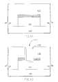
- FIG. 1an anti-reflecting coating 110 is on a first metal layer 100 .
- a dielectric layer 120is blanketed onto the first metal layer 100 and the anti-reflection coating 110 .
- a via 130is fabricated through the dielectric layer 120 and the anti-reflecting coating 110 , and thus portion of the first metal layer 100 is exposed by the via 130 .
- a glue layer 140is deposited into the via 130 , and a secondary metal layer 150 is filled filled into the via 130 .
- FIG. 2Another well-known process for fabricating a metal contact in a semiconductor structure is as shown in FIG. 2.
- the etching process for forming the via 130is stopped on the ARC 110 , and the first metal layer 100 will not be exposed by the via 130 .
- a methodfor preventing metal extrusion during the formation of a metal contact in a semiconductor structure.
- the phenomenon of raising resistance in a semiconductor structurecan be efficient removed by preventing the metal extrusion during the formation of a metal contact.
- the inventionprovides a method for preventing metal extrusion in a semiconductor structure. Due to a thermal process before the formation of the glue layer into a metal via, the phenomenon of metal extrusion in a semiconductor structure can be precluded efficiently. Therefore, this invention provides a method for keeping a semiconductor structure from raising resistance by preventing metal extrusion during the formation of the metal contact.
- FIG. 1is a diagram showing a metal contact fabricated by the method of “through ARC” in the prior art
- FIG. 2is a diagram showing a metal contact fabricated by the method of “stop on ARC” in the prior art
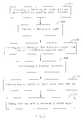
- FIG. 3is a flow chart showing the method for preventing metal extrusion in a semiconductor structure according to this present invention.
- FIGS. 4A to 4 Cshow the method for preventing metal extrusion in a semiconductor structure according to this invention.
- One preferred embodiment of this inventionis a method for preventing metal extrusion.
- a first metal layer with an anti-reflection coating layer thereonis provided on a substrate.
- a dielectric layeris blanketed onto the substrate and the anti-reflection coating layer.
- a viais formed through the dielectric layer and the anti-reflection coating layer, and portion of the first metal layer is exposed by the via.
- a thermal processis performed to extrude the first metal layer.
- the temperature of the above-mentioned thermal processis equal to/higher than the highest temperature of the following process.
- a conformal glue layeris formed into the via.
- the viais filled with a secondary metal layer. Because the thermal process is performed before the formation of the glue layer and the secondary metal layer, the first metal layer will not be extruded by thermal effect during the following processes.
- FIG. 3is a flowchart of the above-mentioned method for preventing metal extrusion.
- a first metal layer with an anti-reflection coating layer thereonis provided on a substrate, as the step 310 .
- the first metal layermay be aluminum (Al).
- the anti-reflection coating layermay be consisted of a Ti layer and a TiN layer.
- a dielectric layeris blanketed onto the substrate and the anti-reflection coating layer.
- the dielectric layermay be SiO 2 , low-K dielectric material, or other dielectric materials.
- the dielectric layer and the anti-reflection coating layerare etched, as the step 330 , and a via is fabricated through the dielectric layer and the anti-reflection coating layer.
- a thermal processis performed as shown in the step 340 .
- the temperature of the thermal process in step 340may be equal to/or higher than the temperature while the formation of the first metal layer.
- the temperature of the thermal process in step 340is equal to/or higher than the highest temperature during the following processes.
- a conformal glue layeris fabricated into the via, as step 350 .
- the glue layermay comprise a Ti layer and a TiN layer.
- a secondary metal layeris filled into the via, and the unwanted secondary metal layer is removed by a ordinary technology as chemical mechanical polishing (CMP).
- the secondary metal layermay be tungsten (W), or other conductive materials.
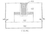
- FIG. 4AAnother preferred embodiment of this present invention is a method for preventing metal extrusion in a semiconductor structure.
- a first metal layer 410is provided on a semiconductor substrate 400 , and an anti-reflection coating layer 420 is formed onto the first metal layer 410 .
- a dielectric layeris blanketed onto the substrate 400 and the anti-reflection coating layer 420 .
- the first metal layer 410may be consisted of aluminum, or other conductive materials.
- the anti-reflection coating layer 420may comprise a Ti layer and a TiN layer, wherein the thickness of the Ti layer is 50 ⁇ 250 angstrom and the thickness of the TiN layer is 200 ⁇ 400 angstrom.
- the dielectric layer 430comprises SiO 2 , low-K dielectric material, or the other dielectric materials.
- the dielectric layer 430 and the anti-reflection coating layer 420are etching for fabricating a via 440 through the dielectric layer 430 and the anti-reflection coating layer 420 , and portion of the first metal layer 410 is exposed by the via 440 .
- an important step of this present inventionis performed. In order to prevent the extrusion of the first metal layer 410 during the following process, the first metal layer 410 is suffered to a thermal process.
- a conformal glue layer 450is fabricated into the via 440 , as shown in FIG. 4B.
- the glue layer 450may comprises a Ti layer and a TiN layer.
- the temperature of the above-mentioned thermal process before the formation of the glue layer 450is a key of this present invention.
- the temperature of the above-mentioned thermal processis equal to/or higher than the temperature during the formation of the first metal layer. More preferably, the temperature of the above-mentioned thermal process is equal to/or higher than the temperature of the processes after the step for forming the via. For example, if the highest temperature during the following processes is the temperature of the glue layer 450 formation at 700 ⁇ 800 degree C., the temperature of the above-mentioned thermal process may be set at 700 ⁇ 800 degree C. or higher.
- a secondary metal layer 460is filled into the via 440 , and the unwanted secondary metal layer 460 is removed by the technology in the prior art, such as chemical mechanical polishing.
- the secondary metal layer 460may be tungsten (W), or the like.
- the secondary metal layer 460is formed by chemical vapor deposition (CVD), or other ordinary process.
- the extrusion of the first metal layerwill not occur by thermal effect during the following processes.
- the side-reaction between the first metal layer and the material of the secondary metal layer as above-cited in the prior artwill not happen during the formation of the secondary metal layer, and the resistance of the semiconductor structure according to this present invention will not be raised.
- this present inventiondiscloses a method for preventing metal extrusion in a semiconductor structure.
- the first metal layeris suffered to a thermal process before fabricating a conformal glue layer into a via, wherein portion of the first metal layer is exposed by the via. Because the temperature of the above-mentioned thermal process is equal to or higher than the highest temperature during the following processes, the first metal layer will not be extruded any more by thermal effect during the following processes.
- the method according to this present inventioncan keep the first metal layer from the side-reaction during the formation of the secondary metal layer into the via.
- this inventionprovides an efficient method for preventing the raising of the resistance in a semiconductor structure due to metal extrusion.
Landscapes
- Engineering & Computer Science (AREA)
- Physics & Mathematics (AREA)
- Condensed Matter Physics & Semiconductors (AREA)
- General Physics & Mathematics (AREA)
- Manufacturing & Machinery (AREA)
- Computer Hardware Design (AREA)
- Microelectronics & Electronic Packaging (AREA)
- Power Engineering (AREA)
- Internal Circuitry In Semiconductor Integrated Circuit Devices (AREA)
Abstract
Description
- 1. Field of the Invention[0001]
- This present invention relates to a method for preventing metal extrusion, and more particularly to a method for preventing metal extrusion in semiconductor structure.[0002]
- 2. Description of the Prior Art[0003]
- In semiconductor structure, metal contact plays a very important role. The metal contacts can connect semiconductor device through metal layers. In the view of one having ordinary skill in the art, metal contacts are usually formed by the follow methods. One method for forming metal contact is “through ARC”. The “through ARC” means the metal via is through the anti-reflection coating (ARC) on the metal layer. As shown in FIG. 1, an[0004]
anti-reflecting coating 110 is on afirst metal layer 100. Adielectric layer 120 is blanketed onto thefirst metal layer 100 and theanti-reflection coating 110. After a etching step, avia 130 is fabricated through thedielectric layer 120 and theanti-reflecting coating 110, and thus portion of thefirst metal layer 100 is exposed by thevia 130. Subsequently, aglue layer 140 is deposited into thevia 130, and asecondary metal layer 150 is filled filled into thevia 130. - Another well-known process for fabricating a metal contact in a semiconductor structure is as shown in FIG. 2. In contrast with the above-mentioned method, the etching process for forming the[0005]
via 130 is stopped on the ARC110, and thefirst metal layer 100 will not be exposed by thevia 130. - However, there are many problems in the above-mentioned methods. In the method of “through ARC”, during the formation of the glue layer and the secondary metal layer, the[0006]
first metal layer 100 will be extruded by the thermal effect and some unwanted reaction may be occurred. In the case of aluminum as thefirst metal layer 100 and tungsten as thesecondary metal layer 150, during the formation of theglue layer 140 and thesecondary metal layer 150, thefirst metal layer 100 will be extruded through theglue layer 140. Moreover, when thesecondary metal layer 150 is fabricated by chemical vapor deposition (CVD) with WF4, the side-reaction between the extruded aluminum and WF4will occur, as the following reaction 1, and the resistance of the semiconductor structure will be raised by theproduce 160 of the reaction 1. - WF4+Al→AlF3 (reaction 1)
- On the other hand, in the above-mentioned method of “stop on ARC”, the reaction 1 will not occur, but the average resistance of the semiconductor structure is higher than the resistance of the semiconductor structure employing the method of “through ARC”. Ordinarily, the method of “through ARC” is utilized wider than the method of “stop on ARC”. Hence, it is important to develop an efficient method for preventing the metal extrusion of the method of “through ARC” in a semiconductor structure.[0007]
- In accordance with the present invention, a method is provided for preventing metal extrusion during the formation of a metal contact in a semiconductor structure. The phenomenon of raising resistance in a semiconductor structure can be efficient removed by preventing the metal extrusion during the formation of a metal contact.[0008]
- In accordance with the above-mentioned objects, the invention provides a method for preventing metal extrusion in a semiconductor structure. Due to a thermal process before the formation of the glue layer into a metal via, the phenomenon of metal extrusion in a semiconductor structure can be precluded efficiently. Therefore, this invention provides a method for keeping a semiconductor structure from raising resistance by preventing metal extrusion during the formation of the metal contact.[0009]
- The foregoing aspects and many of the attendant advantages of this invention will become more readily appreciated as the same becomes better understood by reference to the following detailed description, when taken in conjunction with the accompanying drawings, wherein:[0010]
- FIG. 1 is a diagram showing a metal contact fabricated by the method of “through ARC” in the prior art;[0011]
- FIG. 2 is a diagram showing a metal contact fabricated by the method of “stop on ARC” in the prior art;[0012]
- FIG. 3 is a flow chart showing the method for preventing metal extrusion in a semiconductor structure according to this present invention; and[0013]
- FIGS. 4A to[0014]4C show the method for preventing metal extrusion in a semiconductor structure according to this invention.
- Some sample embodiments of the invention will now be described in greater detail. Nevertheless, it should be recognized that the present invention can be practiced in a wide range of other embodiments besides those explicitly described, and the scope of the present invention is expressly not limited except as specified in the accompanying claims.[0015]
- One preferred embodiment of this invention is a method for preventing metal extrusion. At first, a first metal layer with an anti-reflection coating layer thereon is provided on a substrate. A dielectric layer is blanketed onto the substrate and the anti-reflection coating layer. After an etching step, a via is formed through the dielectric layer and the anti-reflection coating layer, and portion of the first metal layer is exposed by the via. Subsequently, a thermal process is performed to extrude the first metal layer. The temperature of the above-mentioned thermal process is equal to/higher than the highest temperature of the following process. Following the thermal process, a conformal glue layer is formed into the via. Finally, the via is filled with a secondary metal layer. Because the thermal process is performed before the formation of the glue layer and the secondary metal layer, the first metal layer will not be extruded by thermal effect during the following processes.[0016]
- Another preferred embodiment according to this present invention is a method for preventing metal extrusion in a semiconductor structure. FIG. 3 is a flowchart of the above-mentioned method for preventing metal extrusion. At first, a first metal layer with an anti-reflection coating layer thereon is provided on a substrate, as the[0017]
step 310. The first metal layer may be aluminum (Al). The anti-reflection coating layer may be consisted of a Ti layer and a TiN layer. As shown in thestep 320, a dielectric layer is blanketed onto the substrate and the anti-reflection coating layer. The dielectric layer may be SiO2, low-K dielectric material, or other dielectric materials. - Next, the dielectric layer and the anti-reflection coating layer are etched, as the[0018]
step 330, and a via is fabricated through the dielectric layer and the anti-reflection coating layer. After the formation of the via, part of the first metal layer is exposed by the via. Subsequently, a thermal process is performed as shown in thestep 340. In order to prevent the extrusion of the first metal layer by thermal effect during the following process, the temperature of the thermal process instep 340 may be equal to/or higher than the temperature while the formation of the first metal layer. Preferably, the temperature of the thermal process instep 340 is equal to/or higher than the highest temperature during the following processes. - After the thermal process, a conformal glue layer is fabricated into the via, as[0019]
step 350. The glue layer may comprise a Ti layer and a TiN layer. Finally, as shown in step260, a secondary metal layer is filled into the via, and the unwanted secondary metal layer is removed by a ordinary technology as chemical mechanical polishing (CMP). The secondary metal layer may be tungsten (W), or other conductive materials. - Another preferred embodiment of this present invention is a method for preventing metal extrusion in a semiconductor structure. Referred to FIG. 4A, a[0020]
first metal layer 410 is provided on asemiconductor substrate 400, and ananti-reflection coating layer 420 is formed onto thefirst metal layer 410. A dielectric layer is blanketed onto thesubstrate 400 and theanti-reflection coating layer 420. In this manner, thefirst metal layer 410 may be consisted of aluminum, or other conductive materials. Theanti-reflection coating layer 420 may comprise a Ti layer and a TiN layer, wherein the thickness of the Ti layer is 50˜250 angstrom and the thickness of the TiN layer is 200˜400 angstrom. Thedielectric layer 430 comprises SiO2, low-K dielectric material, or the other dielectric materials. - Subsequently, the[0021]
dielectric layer 430 and theanti-reflection coating layer 420 are etching for fabricating a via440 through thedielectric layer 430 and theanti-reflection coating layer 420, and portion of thefirst metal layer 410 is exposed by thevia 440. After fabricating the via440, an important step of this present invention is performed. In order to prevent the extrusion of thefirst metal layer 410 during the following process, thefirst metal layer 410 is suffered to a thermal process. Next, aconformal glue layer 450 is fabricated into the via440, as shown in FIG. 4B. Theglue layer 450 may comprises a Ti layer and a TiN layer. - The temperature of the above-mentioned thermal process before the formation of the[0022]
glue layer 450 is a key of this present invention. Preferably, the temperature of the above-mentioned thermal process is equal to/or higher than the temperature during the formation of the first metal layer. More preferably, the temperature of the above-mentioned thermal process is equal to/or higher than the temperature of the processes after the step for forming the via. For example, if the highest temperature during the following processes is the temperature of theglue layer 450 formation at 700˜800 degree C., the temperature of the above-mentioned thermal process may be set at 700˜800 degree C. or higher. - As shown in FIG. 4C, a[0023]
secondary metal layer 460 is filled into the via440, and the unwantedsecondary metal layer 460 is removed by the technology in the prior art, such as chemical mechanical polishing. Thesecondary metal layer 460 may be tungsten (W), or the like. Thesecondary metal layer 460 is formed by chemical vapor deposition (CVD), or other ordinary process. - According to this preferred embodiment, because the first metal layer is suffered to a thermal process before the fabricating of the glue layer, the extrusion of the first metal layer will not occur by thermal effect during the following processes. Thus, the side-reaction between the first metal layer and the material of the secondary metal layer as above-cited in the prior art will not happen during the formation of the secondary metal layer, and the resistance of the semiconductor structure according to this present invention will not be raised.[0024]
- According to the preferred embodiments, this present invention discloses a method for preventing metal extrusion in a semiconductor structure. The first metal layer is suffered to a thermal process before fabricating a conformal glue layer into a via, wherein portion of the first metal layer is exposed by the via. Because the temperature of the above-mentioned thermal process is equal to or higher than the highest temperature during the following processes, the first metal layer will not be extruded any more by thermal effect during the following processes. Moreover, the method according to this present invention can keep the first metal layer from the side-reaction during the formation of the secondary metal layer into the via. Thus, this invention provides an efficient method for preventing the raising of the resistance in a semiconductor structure due to metal extrusion.[0025]
- Although specific embodiments have been illustrated and described, it will be obvious to those skilled in the art that various modifications may be made without departing from what is intended to be limited solely by the appended claims.[0026]
Claims (21)
1. A method for preventing metal extrusion, comprising:
providing a first metal layer;
forming a dielectric layer onto said first metal layer;
etching said dielectric layer to form a via onto said first metal layer;
performing a thermal process; and
depositing a conformal glue layer into said via.
2. The method according toclaim 1 , further comprises forming a anti-reflection coating layer onto said first metal layer before the step for forming said dielectric layer.
3. The method according toclaim 2 , wherein said via is through said dielectric layer and said anti-reflection coating layer.
4. The method according toclaim 1 , wherein said thermal process is performed at a temperature higher than the temperature during said step for providing said first metal layer.
5. The method according toclaim 1 , wherein said thermal process is performed at a temperature equal to the highest temperature during a plurality of process following the step for etching said dielectric layer.
6. The method according toclaim 1 , wherein said thermal process is performed at a temperature higher than the highest temperature during a plurality of process following the step for etching said dielectric layer.
7. The method according toclaim 1 , further comprises filling said via with a secondary metal layer.
8. A method for preventing metal extrusion in a semiconductor structure, comprising:
providing a first metal layer with an anti-reflection coating layer thereon;
forming a dielectric layer onto said anti-reflection coating layer;
etching said dielectric layer and said anti-reflection coating layer to form a via exposing said first metal layer;
performing a thermal process;
depositing a conformal glue layer into said via; and
filling said via with a secondary metal layer.
9. The method according toclaim 8 , wherein said thermal process is performed at a temperature higher than the temperature of said step for providing said first metal layer.
10. The method according toclaim 8 , wherein said thermal process is performed at a temperature equal to the highest temperature during a plurality of process following the step for etching said dielectric layer and said anti-reflection coating layer.
11. The method according toclaim 8 , wherein said thermal process is performed at a temperature higher than the highest temperature during a plurality of process following the step for etching said dielectric layer and said anti-reflection coating layer.
12. The method according toclaim 8 , wherein said first metal layer is aluminum.
13. The method according toclaim 8 , wherein said anti-reflection coating layer comprises a Ti layer.
14. The method according toclaim 8 , wherein said anti-reflection coating layer comprises a TiN layer.
15. The method according toclaim 8 , wherein said secondary metal layer is tungsten.
16. A method for preventing metal extrusion in a semiconductor structure, comprising:
providing an aluminum layer on a substrate;
forming an anti-reflection coating layer onto said aluminum layer;
forming a dielectric layer onto said substrate and said anti-reflection coating layer;
etching said dielectric layer and said anti-reflection coating layer to form a via exposing said aluminum layer;
performing a thermal process;
depositing a conformal glue layer into said via; and
filling said via with a tungsten layer.
17. The method according toclaim 16 , wherein said thermal process is performed at a temperature higher than the temperature of said step for providing said aluminum layer.
18. The method according toclaim 16 , wherein said thermal process is performed at a temperature equal to the highest temperature during a plurality of process following the step for etching said dielectric layer and said anti-reflection coating layer.
19. The method according toclaim 16 , wherein said thermal process is performed at a temperature higher than the highest temperature during a plurality of process following the step for etching said dielectric layer and said anti-reflection coating layer.
20. The method according toclaim 16 , wherein said glue layer comprises a Ti layer.
21. The method according toclaim 16 , wherein said glue layer comprises a TiN layer.
Priority Applications (2)
| Application Number | Priority Date | Filing Date | Title |
|---|---|---|---|
| US10/214,145US20040058531A1 (en) | 2002-08-08 | 2002-08-08 | Method for preventing metal extrusion in a semiconductor structure. |
| CNA031331351ACN1476076A (en) | 2002-08-08 | 2003-07-24 | method for preventing metal extrusion |
Applications Claiming Priority (1)
| Application Number | Priority Date | Filing Date | Title |
|---|---|---|---|
| US10/214,145US20040058531A1 (en) | 2002-08-08 | 2002-08-08 | Method for preventing metal extrusion in a semiconductor structure. |
Publications (1)
| Publication Number | Publication Date |
|---|---|
| US20040058531A1true US20040058531A1 (en) | 2004-03-25 |
Family
ID=31494618
Family Applications (1)
| Application Number | Title | Priority Date | Filing Date |
|---|---|---|---|
| US10/214,145AbandonedUS20040058531A1 (en) | 2002-08-08 | 2002-08-08 | Method for preventing metal extrusion in a semiconductor structure. |
Country Status (2)
| Country | Link |
|---|---|
| US (1) | US20040058531A1 (en) |
| CN (1) | CN1476076A (en) |
Cited By (46)
| Publication number | Priority date | Publication date | Assignee | Title |
|---|---|---|---|---|
| US20040058532A1 (en)* | 2002-09-20 | 2004-03-25 | Miles Mark W. | Controlling electromechanical behavior of structures within a microelectromechanical systems device |
| US20050046922A1 (en)* | 2003-09-03 | 2005-03-03 | Wen-Jian Lin | Interferometric modulation pixels and manufacturing method thereof |
| US20060006138A1 (en)* | 2003-08-26 | 2006-01-12 | Wen-Jian Lin | Interference display cell and fabrication method thereof |
| US20060066932A1 (en)* | 2004-09-27 | 2006-03-30 | Clarence Chui | Method of selective etching using etch stop layer |
| US20060065622A1 (en)* | 2004-09-27 | 2006-03-30 | Floyd Philip D | Method and system for xenon fluoride etching with enhanced efficiency |
| US20060067650A1 (en)* | 2004-09-27 | 2006-03-30 | Clarence Chui | Method of making a reflective display device using thin film transistor production techniques |
| US20060065366A1 (en)* | 2004-09-27 | 2006-03-30 | Cummings William J | Portable etch chamber |
| US20060067644A1 (en)* | 2004-09-27 | 2006-03-30 | Clarence Chui | Method of fabricating interferometric devices using lift-off processing techniques |
| US20060077518A1 (en)* | 2004-09-27 | 2006-04-13 | Clarence Chui | Mirror and mirror layer for optical modulator and method |
| US20060077519A1 (en)* | 2004-09-27 | 2006-04-13 | Floyd Philip D | System and method for providing thermal compensation for an interferometric modulator display |
| US20060077151A1 (en)* | 2004-09-27 | 2006-04-13 | Clarence Chui | Method and device for a display having transparent components integrated therein |
| US20060077528A1 (en)* | 2004-09-27 | 2006-04-13 | Floyd Philip D | Device and method for modifying actuation voltage thresholds of a deformable membrane in an interferometric modulator |
| US20060076311A1 (en)* | 2004-09-27 | 2006-04-13 | Ming-Hau Tung | Methods of fabricating interferometric modulators by selectively removing a material |
| US20060177950A1 (en)* | 2005-02-04 | 2006-08-10 | Wen-Jian Lin | Method of manufacturing optical interferance color display |
| US20060256420A1 (en)* | 2003-06-24 | 2006-11-16 | Miles Mark W | Film stack for manufacturing micro-electromechanical systems (MEMS) devices |
| US20060257070A1 (en)* | 2003-05-26 | 2006-11-16 | Wen-Jian Lin | Optical interference display cell and method of making the same |
| US20070041079A1 (en)* | 2004-09-27 | 2007-02-22 | Clarence Chui | Interferometric modulators having charge persistence |
| US20070155051A1 (en)* | 2005-12-29 | 2007-07-05 | Chun-Ming Wang | Method of creating MEMS device cavities by a non-etching process |
| US20070170540A1 (en)* | 2006-01-18 | 2007-07-26 | Chung Won Suk | Silicon-rich silicon nitrides as etch stops in MEMS manufature |
| US7250315B2 (en) | 2002-02-12 | 2007-07-31 | Idc, Llc | Method for fabricating a structure for a microelectromechanical system (MEMS) device |
| US20070228156A1 (en)* | 2006-03-28 | 2007-10-04 | Household Corporation | Interoperability facilitator |
| US20070236774A1 (en)* | 2006-04-10 | 2007-10-11 | Evgeni Gousev | Interferometric optical display system with broadband characteristics |
| US20070247696A1 (en)* | 2006-04-19 | 2007-10-25 | Teruo Sasagawa | Microelectromechanical device and method utilizing a porous surface |
| US20070247401A1 (en)* | 2006-04-19 | 2007-10-25 | Teruo Sasagawa | Microelectromechanical device and method utilizing nanoparticles |
| US7291921B2 (en) | 2003-09-30 | 2007-11-06 | Qualcomm Mems Technologies, Inc. | Structure of a micro electro mechanical system and the manufacturing method thereof |
| US20070258123A1 (en)* | 2006-05-03 | 2007-11-08 | Gang Xu | Electrode and interconnect materials for MEMS devices |
| US7297471B1 (en) | 2003-04-15 | 2007-11-20 | Idc, Llc | Method for manufacturing an array of interferometric modulators |
| US20070279730A1 (en)* | 2006-06-01 | 2007-12-06 | David Heald | Process and structure for fabrication of mems device having isolated egde posts |
| US20080032439A1 (en)* | 2006-08-02 | 2008-02-07 | Xiaoming Yan | Selective etching of MEMS using gaseous halides and reactive co-etchants |
| US20080093688A1 (en)* | 2004-09-27 | 2008-04-24 | Idc, Llc | Process for modifying offset voltage characteristics of an interferometric modulator |
| US7373026B2 (en) | 2004-09-27 | 2008-05-13 | Idc, Llc | MEMS device fabricated on a pre-patterned substrate |
| US7405861B2 (en) | 2004-09-27 | 2008-07-29 | Idc, Llc | Method and device for protecting interferometric modulators from electrostatic discharge |
| US7405863B2 (en) | 2006-06-01 | 2008-07-29 | Qualcomm Mems Technologies, Inc. | Patterning of mechanical layer in MEMS to reduce stresses at supports |
| US20080218840A1 (en)* | 2005-08-19 | 2008-09-11 | Chengin Qui | Methods for etching layers within a MEMS device to achieve a tapered edge |
| US20080231931A1 (en)* | 2007-03-21 | 2008-09-25 | Qualcomm Incorporated | Mems cavity-coating layers and methods |
| US7450295B2 (en) | 2006-03-02 | 2008-11-11 | Qualcomm Mems Technologies, Inc. | Methods for producing MEMS with protective coatings using multi-component sacrificial layers |
| US20090040590A1 (en)* | 2007-08-07 | 2009-02-12 | Qualcomm Technologies, Inc. | Mems device and interconnects for same |
| US7492502B2 (en) | 2004-09-27 | 2009-02-17 | Idc, Llc | Method of fabricating a free-standing microstructure |
| US7527996B2 (en) | 2006-04-19 | 2009-05-05 | Qualcomm Mems Technologies, Inc. | Non-planar surface structures and process for microelectromechanical systems |
| US7535621B2 (en) | 2006-12-27 | 2009-05-19 | Qualcomm Mems Technologies, Inc. | Aluminum fluoride films for microelectromechanical system applications |
| US7567373B2 (en) | 2004-07-29 | 2009-07-28 | Idc, Llc | System and method for micro-electromechanical operation of an interferometric modulator |
| US7580172B2 (en) | 2005-09-30 | 2009-08-25 | Qualcomm Mems Technologies, Inc. | MEMS device and interconnects for same |
| US7781850B2 (en) | 2002-09-20 | 2010-08-24 | Qualcomm Mems Technologies, Inc. | Controlling electromechanical behavior of structures within a microelectromechanical systems device |
| US8830557B2 (en) | 2007-05-11 | 2014-09-09 | Qualcomm Mems Technologies, Inc. | Methods of fabricating MEMS with spacers between plates and devices formed by same |
| US20140291802A1 (en)* | 2013-03-29 | 2014-10-02 | International Business Machines Corporation | Semiconductor structures with metal lines |
| US20220199464A1 (en)* | 2020-12-21 | 2022-06-23 | Infineon Technologies Ag | Semiconductor device protection |
Citations (1)
| Publication number | Priority date | Publication date | Assignee | Title |
|---|---|---|---|---|
| US6037278A (en)* | 1996-08-30 | 2000-03-14 | Nec Corporation | Method of manufacturing semiconductor devices having multi-level wiring structure |
- 2002
- 2002-08-08USUS10/214,145patent/US20040058531A1/ennot_activeAbandoned
- 2003
- 2003-07-24CNCNA031331351Apatent/CN1476076A/enactivePending
Patent Citations (1)
| Publication number | Priority date | Publication date | Assignee | Title |
|---|---|---|---|---|
| US6037278A (en)* | 1996-08-30 | 2000-03-14 | Nec Corporation | Method of manufacturing semiconductor devices having multi-level wiring structure |
Cited By (78)
| Publication number | Priority date | Publication date | Assignee | Title |
|---|---|---|---|---|
| US7642110B2 (en) | 2002-02-12 | 2010-01-05 | Qualcomm Mems Technologies, Inc. | Method for fabricating a structure for a microelectromechanical systems (MEMS) device |
| US7250315B2 (en) | 2002-02-12 | 2007-07-31 | Idc, Llc | Method for fabricating a structure for a microelectromechanical system (MEMS) device |
| US7781850B2 (en) | 2002-09-20 | 2010-08-24 | Qualcomm Mems Technologies, Inc. | Controlling electromechanical behavior of structures within a microelectromechanical systems device |
| US20040058532A1 (en)* | 2002-09-20 | 2004-03-25 | Miles Mark W. | Controlling electromechanical behavior of structures within a microelectromechanical systems device |
| US7297471B1 (en) | 2003-04-15 | 2007-11-20 | Idc, Llc | Method for manufacturing an array of interferometric modulators |
| US20060257070A1 (en)* | 2003-05-26 | 2006-11-16 | Wen-Jian Lin | Optical interference display cell and method of making the same |
| US20060256420A1 (en)* | 2003-06-24 | 2006-11-16 | Miles Mark W | Film stack for manufacturing micro-electromechanical systems (MEMS) devices |
| US20060006138A1 (en)* | 2003-08-26 | 2006-01-12 | Wen-Jian Lin | Interference display cell and fabrication method thereof |
| US7485236B2 (en) | 2003-08-26 | 2009-02-03 | Qualcomm Mems Technologies, Inc. | Interference display cell and fabrication method thereof |
| US20050046922A1 (en)* | 2003-09-03 | 2005-03-03 | Wen-Jian Lin | Interferometric modulation pixels and manufacturing method thereof |
| US7291921B2 (en) | 2003-09-30 | 2007-11-06 | Qualcomm Mems Technologies, Inc. | Structure of a micro electro mechanical system and the manufacturing method thereof |
| US7567373B2 (en) | 2004-07-29 | 2009-07-28 | Idc, Llc | System and method for micro-electromechanical operation of an interferometric modulator |
| US20060077528A1 (en)* | 2004-09-27 | 2006-04-13 | Floyd Philip D | Device and method for modifying actuation voltage thresholds of a deformable membrane in an interferometric modulator |
| US20060067650A1 (en)* | 2004-09-27 | 2006-03-30 | Clarence Chui | Method of making a reflective display device using thin film transistor production techniques |
| US20060076311A1 (en)* | 2004-09-27 | 2006-04-13 | Ming-Hau Tung | Methods of fabricating interferometric modulators by selectively removing a material |
| US7429334B2 (en) | 2004-09-27 | 2008-09-30 | Idc, Llc | Methods of fabricating interferometric modulators by selectively removing a material |
| US20070041079A1 (en)* | 2004-09-27 | 2007-02-22 | Clarence Chui | Interferometric modulators having charge persistence |
| US20060066932A1 (en)* | 2004-09-27 | 2006-03-30 | Clarence Chui | Method of selective etching using etch stop layer |
| US20060077151A1 (en)* | 2004-09-27 | 2006-04-13 | Clarence Chui | Method and device for a display having transparent components integrated therein |
| US20060077519A1 (en)* | 2004-09-27 | 2006-04-13 | Floyd Philip D | System and method for providing thermal compensation for an interferometric modulator display |
| US8126297B2 (en) | 2004-09-27 | 2012-02-28 | Qualcomm Mems Technologies, Inc. | MEMS device fabricated on a pre-patterned substrate |
| US7830589B2 (en) | 2004-09-27 | 2010-11-09 | Qualcomm Mems Technologies, Inc. | Device and method for modifying actuation voltage thresholds of a deformable membrane in an interferometric modulator |
| US7420728B2 (en) | 2004-09-27 | 2008-09-02 | Idc, Llc | Methods of fabricating interferometric modulators by selectively removing a material |
| US20060077518A1 (en)* | 2004-09-27 | 2006-04-13 | Clarence Chui | Mirror and mirror layer for optical modulator and method |
| US20060067644A1 (en)* | 2004-09-27 | 2006-03-30 | Clarence Chui | Method of fabricating interferometric devices using lift-off processing techniques |
| US20100129025A1 (en)* | 2004-09-27 | 2010-05-27 | Qualcomm Mems Technologies, Inc. | Mems device fabricated on a pre-patterned substrate |
| US20060065366A1 (en)* | 2004-09-27 | 2006-03-30 | Cummings William J | Portable etch chamber |
| US20100079849A1 (en)* | 2004-09-27 | 2010-04-01 | Qualcomm Mems Technologies, Inc. | Device and method for modifying actuation voltage thresholds of a deformable membrane in an interferometric modulator |
| US7660031B2 (en) | 2004-09-27 | 2010-02-09 | Qualcomm Mems Technologies, Inc. | Device and method for modifying actuation voltage thresholds of a deformable membrane in an interferometric modulator |
| US7492502B2 (en) | 2004-09-27 | 2009-02-17 | Idc, Llc | Method of fabricating a free-standing microstructure |
| US7417783B2 (en) | 2004-09-27 | 2008-08-26 | Idc, Llc | Mirror and mirror layer for optical modulator and method |
| US7349136B2 (en) | 2004-09-27 | 2008-03-25 | Idc, Llc | Method and device for a display having transparent components integrated therein |
| US20080093688A1 (en)* | 2004-09-27 | 2008-04-24 | Idc, Llc | Process for modifying offset voltage characteristics of an interferometric modulator |
| US20060065622A1 (en)* | 2004-09-27 | 2006-03-30 | Floyd Philip D | Method and system for xenon fluoride etching with enhanced efficiency |
| US7369296B2 (en) | 2004-09-27 | 2008-05-06 | Idc, Llc | Device and method for modifying actuation voltage thresholds of a deformable membrane in an interferometric modulator |
| US7373026B2 (en) | 2004-09-27 | 2008-05-13 | Idc, Llc | MEMS device fabricated on a pre-patterned substrate |
| US7532386B2 (en) | 2004-09-27 | 2009-05-12 | Idc, Llc | Process for modifying offset voltage characteristics of an interferometric modulator |
| US20080144163A1 (en)* | 2004-09-27 | 2008-06-19 | Idc, Llc | Device and method for modifying actuation voltage thresholds of a deformable membrane in an interferometric modulator |
| US7405861B2 (en) | 2004-09-27 | 2008-07-29 | Idc, Llc | Method and device for protecting interferometric modulators from electrostatic discharge |
| US7547565B2 (en) | 2005-02-04 | 2009-06-16 | Qualcomm Mems Technologies, Inc. | Method of manufacturing optical interference color display |
| US20060177950A1 (en)* | 2005-02-04 | 2006-08-10 | Wen-Jian Lin | Method of manufacturing optical interferance color display |
| US20080218840A1 (en)* | 2005-08-19 | 2008-09-11 | Chengin Qui | Methods for etching layers within a MEMS device to achieve a tapered edge |
| US7580172B2 (en) | 2005-09-30 | 2009-08-25 | Qualcomm Mems Technologies, Inc. | MEMS device and interconnects for same |
| US7795061B2 (en) | 2005-12-29 | 2010-09-14 | Qualcomm Mems Technologies, Inc. | Method of creating MEMS device cavities by a non-etching process |
| US20070155051A1 (en)* | 2005-12-29 | 2007-07-05 | Chun-Ming Wang | Method of creating MEMS device cavities by a non-etching process |
| US20070170540A1 (en)* | 2006-01-18 | 2007-07-26 | Chung Won Suk | Silicon-rich silicon nitrides as etch stops in MEMS manufature |
| US7382515B2 (en) | 2006-01-18 | 2008-06-03 | Qualcomm Mems Technologies, Inc. | Silicon-rich silicon nitrides as etch stops in MEMS manufacture |
| US7450295B2 (en) | 2006-03-02 | 2008-11-11 | Qualcomm Mems Technologies, Inc. | Methods for producing MEMS with protective coatings using multi-component sacrificial layers |
| US20070228156A1 (en)* | 2006-03-28 | 2007-10-04 | Household Corporation | Interoperability facilitator |
| US20070236774A1 (en)* | 2006-04-10 | 2007-10-11 | Evgeni Gousev | Interferometric optical display system with broadband characteristics |
| US20100128339A1 (en)* | 2006-04-10 | 2010-05-27 | Qualcomm Mems Technologies, Inc. | Interferometric optical display system with broadband characteristics |
| US20080030825A1 (en)* | 2006-04-19 | 2008-02-07 | Qualcomm Incorporated | Microelectromechanical device and method utilizing a porous surface |
| US7527996B2 (en) | 2006-04-19 | 2009-05-05 | Qualcomm Mems Technologies, Inc. | Non-planar surface structures and process for microelectromechanical systems |
| US20070247401A1 (en)* | 2006-04-19 | 2007-10-25 | Teruo Sasagawa | Microelectromechanical device and method utilizing nanoparticles |
| US7711239B2 (en) | 2006-04-19 | 2010-05-04 | Qualcomm Mems Technologies, Inc. | Microelectromechanical device and method utilizing nanoparticles |
| US7564613B2 (en) | 2006-04-19 | 2009-07-21 | Qualcomm Mems Technologies, Inc. | Microelectromechanical device and method utilizing a porous surface |
| US20070247696A1 (en)* | 2006-04-19 | 2007-10-25 | Teruo Sasagawa | Microelectromechanical device and method utilizing a porous surface |
| US7417784B2 (en) | 2006-04-19 | 2008-08-26 | Qualcomm Mems Technologies, Inc. | Microelectromechanical device and method utilizing a porous surface |
| US7369292B2 (en) | 2006-05-03 | 2008-05-06 | Qualcomm Mems Technologies, Inc. | Electrode and interconnect materials for MEMS devices |
| US20070258123A1 (en)* | 2006-05-03 | 2007-11-08 | Gang Xu | Electrode and interconnect materials for MEMS devices |
| US20080239449A1 (en)* | 2006-05-03 | 2008-10-02 | Qualcomm Mems Technologies, Inc. | Electrode and interconnect materials for mems devices |
| US7405863B2 (en) | 2006-06-01 | 2008-07-29 | Qualcomm Mems Technologies, Inc. | Patterning of mechanical layer in MEMS to reduce stresses at supports |
| US7321457B2 (en) | 2006-06-01 | 2008-01-22 | Qualcomm Incorporated | Process and structure for fabrication of MEMS device having isolated edge posts |
| US20070279730A1 (en)* | 2006-06-01 | 2007-12-06 | David Heald | Process and structure for fabrication of mems device having isolated egde posts |
| US20080032439A1 (en)* | 2006-08-02 | 2008-02-07 | Xiaoming Yan | Selective etching of MEMS using gaseous halides and reactive co-etchants |
| US7566664B2 (en) | 2006-08-02 | 2009-07-28 | Qualcomm Mems Technologies, Inc. | Selective etching of MEMS using gaseous halides and reactive co-etchants |
| US7535621B2 (en) | 2006-12-27 | 2009-05-19 | Qualcomm Mems Technologies, Inc. | Aluminum fluoride films for microelectromechanical system applications |
| US7733552B2 (en) | 2007-03-21 | 2010-06-08 | Qualcomm Mems Technologies, Inc | MEMS cavity-coating layers and methods |
| US20100245979A1 (en)* | 2007-03-21 | 2010-09-30 | Qualcomm Mems Technologies, Inc. | Mems cavity-coating layers and methods |
| US20080231931A1 (en)* | 2007-03-21 | 2008-09-25 | Qualcomm Incorporated | Mems cavity-coating layers and methods |
| US8164815B2 (en) | 2007-03-21 | 2012-04-24 | Qualcomm Mems Technologies, Inc. | MEMS cavity-coating layers and methods |
| US8830557B2 (en) | 2007-05-11 | 2014-09-09 | Qualcomm Mems Technologies, Inc. | Methods of fabricating MEMS with spacers between plates and devices formed by same |
| US7570415B2 (en) | 2007-08-07 | 2009-08-04 | Qualcomm Mems Technologies, Inc. | MEMS device and interconnects for same |
| US20090040590A1 (en)* | 2007-08-07 | 2009-02-12 | Qualcomm Technologies, Inc. | Mems device and interconnects for same |
| US20140291802A1 (en)* | 2013-03-29 | 2014-10-02 | International Business Machines Corporation | Semiconductor structures with metal lines |
| US9087839B2 (en)* | 2013-03-29 | 2015-07-21 | International Business Machines Corporation | Semiconductor structures with metal lines |
| US20220199464A1 (en)* | 2020-12-21 | 2022-06-23 | Infineon Technologies Ag | Semiconductor device protection |
| US12046509B2 (en)* | 2020-12-21 | 2024-07-23 | Infineon Technologies Ag | Semiconductor device protection using an anti-reflective layer |
Also Published As
| Publication number | Publication date |
|---|---|
| CN1476076A (en) | 2004-02-18 |
Similar Documents
| Publication | Publication Date | Title |
|---|---|---|
| US20040058531A1 (en) | Method for preventing metal extrusion in a semiconductor structure. | |
| US6447933B1 (en) | Formation of alloy material using alternating depositions of alloy doping element and bulk material | |
| US5963827A (en) | Method for producing via contacts in a semiconductor device | |
| US20030091870A1 (en) | Method of forming a liner for tungsten plugs | |
| US6225213B1 (en) | Manufacturing method for contact hole | |
| US5963828A (en) | Method for tungsten nucleation from WF6 using titanium as a reducing agent | |
| US20030054628A1 (en) | Method of forming a low resistance multi-layered TiN film with superior barrier property using poison mode cycling | |
| US6258720B1 (en) | Method of formation of conductive lines on integrated circuits | |
| CN1125481C (en) | Manufacturing method of semiconductor element avoiding tungsten plug loss barrier layer | |
| US8587128B2 (en) | Damascene structure | |
| US20070152334A1 (en) | Semiconductor device and manufacturing method | |
| US6747354B2 (en) | Semiconductor devices having multilevel interconnections and methods for manufacturing the same | |
| US6443743B1 (en) | Method for reducing via resistance in small high aspect ratio holes filled using aluminum extrusion | |
| US20030186498A1 (en) | Method for fabricating metal interconnection with reliability using ionized physical vapor deposition | |
| GB2314679A (en) | Method of forming a plug in a semiconductor device | |
| US6841442B1 (en) | Method for forming metal contact of semiconductor device | |
| US20030100184A1 (en) | Method of forming a semiconductor device with a multi-layer WSix film with small grain size structure, and a semiconductor device having a polysilicon layer with a multi-layer WSix film formed thereon | |
| US6316355B1 (en) | Method for forming metal wire using titanium film in semiconductor device having contact holes | |
| US6962877B2 (en) | Methods of preventing oxidation of barrier metal of semiconductor devices | |
| US9754879B2 (en) | Integrated circuitry | |
| KR950005259B1 (en) | Fabricating method of semiconductor device | |
| JP3288010B2 (en) | Method for forming metal wiring of semiconductor device | |
| US6309963B1 (en) | Method for manufacturing semiconductor device | |
| JPH0974095A (en) | Method for manufacturing semiconductor device | |
| JP2000077417A (en) | Formation of wiring of semiconductor element |
Legal Events
| Date | Code | Title | Description |
|---|---|---|---|
| AS | Assignment | Owner name:UNITED MICROELECTRONICS CORP., TAIWAN Free format text:ASSIGNMENT OF ASSIGNORS INTEREST;ASSIGNORS:HSIEH, YEN-WU;LEE, SHIH-LUNG;WU, BER;AND OTHERS;REEL/FRAME:013178/0340 Effective date:20020730 | |
| STCB | Information on status: application discontinuation | Free format text:ABANDONED -- FAILURE TO RESPOND TO AN OFFICE ACTION |