US20040058488A1 - Monitoring system comprising infrared thermopile detetor - Google Patents
Monitoring system comprising infrared thermopile detetorDownload PDFInfo
- Publication number
- US20040058488A1 US20040058488A1US10/668,489US66848903AUS2004058488A1US 20040058488 A1US20040058488 A1US 20040058488A1US 66848903 AUS66848903 AUS 66848903AUS 2004058488 A1US2004058488 A1US 2004058488A1
- Authority
- US
- United States
- Prior art keywords
- infrared radiation
- semiconductor process
- sampling region
- thermopile detector
- process system
- Prior art date
- Legal status (The legal status is an assumption and is not a legal conclusion. Google has not performed a legal analysis and makes no representation as to the accuracy of the status listed.)
- Granted
Links
- 238000012544monitoring processMethods0.000titledescription8
- 239000004065semiconductorSubstances0.000claimsabstractdescription66
- 230000005540biological transmissionEffects0.000claimsabstractdescription64
- 238000005070samplingMethods0.000claimsabstractdescription64
- 239000000463materialSubstances0.000claimsabstractdescription49
- 238000012545processingMethods0.000claimsabstractdescription13
- 238000010521absorption reactionMethods0.000claimsabstractdescription11
- 238000004886process controlMethods0.000claimsabstractdescription8
- 238000000034methodMethods0.000claimsdescription114
- 230000005855radiationEffects0.000claimsdescription108
- 230000008569processEffects0.000claimsdescription103
- 239000007789gasSubstances0.000claimsdescription99
- 238000010926purgeMethods0.000claimsdescription34
- 239000002245particleSubstances0.000claimsdescription25
- 238000000151depositionMethods0.000claimsdescription9
- 230000008021depositionEffects0.000claimsdescription8
- ABTOQLMXBSRXSM-UHFFFAOYSA-Nsilicon tetrafluorideChemical compoundF[Si](F)(F)FABTOQLMXBSRXSM-UHFFFAOYSA-N0.000claimsdescription7
- 238000011144upstream manufacturingMethods0.000claimsdescription7
- XYFCBTPGUUZFHI-UHFFFAOYSA-NPhosphineChemical compoundPXYFCBTPGUUZFHI-UHFFFAOYSA-N0.000claimsdescription6
- 238000010438heat treatmentMethods0.000claimsdescription5
- XKRFYHLGVUSROY-UHFFFAOYSA-NArgonChemical compound[Ar]XKRFYHLGVUSROY-UHFFFAOYSA-N0.000claimsdescription4
- GQPLMRYTRLFLPF-UHFFFAOYSA-NNitrous OxideChemical compound[O-][N+]#NGQPLMRYTRLFLPF-UHFFFAOYSA-N0.000claimsdescription4
- BOTDANWDWHJENH-UHFFFAOYSA-NTetraethyl orthosilicateChemical compoundCCO[Si](OCC)(OCC)OCCBOTDANWDWHJENH-UHFFFAOYSA-N0.000claimsdescription4
- 238000000623plasma-assisted chemical vapour depositionMethods0.000claimsdescription4
- 238000002310reflectometryMethods0.000claimsdescription4
- 239000000126substanceSubstances0.000claimsdescription4
- ZAMOUSCENKQFHK-UHFFFAOYSA-NChlorine atomChemical compound[Cl]ZAMOUSCENKQFHK-UHFFFAOYSA-N0.000claimsdescription3
- BLRPTPMANUNPDV-UHFFFAOYSA-NSilaneChemical compound[SiH4]BLRPTPMANUNPDV-UHFFFAOYSA-N0.000claimsdescription3
- RBFQJDQYXXHULB-UHFFFAOYSA-NarsaneChemical compound[AsH3]RBFQJDQYXXHULB-UHFFFAOYSA-N0.000claimsdescription3
- 230000015572biosynthetic processEffects0.000claimsdescription3
- 239000000460chlorineSubstances0.000claimsdescription3
- 229910052801chlorineInorganic materials0.000claimsdescription3
- 239000012530fluidSubstances0.000claimsdescription3
- 229910000073phosphorus hydrideInorganic materials0.000claimsdescription3
- 229910000077silaneInorganic materials0.000claimsdescription3
- QGZKDVFQNNGYKY-UHFFFAOYSA-OAmmoniumChemical compound[NH4+]QGZKDVFQNNGYKY-UHFFFAOYSA-O0.000claimsdescription2
- KRHYYFGTRYWZRS-UHFFFAOYSA-NFluoraneChemical compoundFKRHYYFGTRYWZRS-UHFFFAOYSA-N0.000claimsdescription2
- PXGOKWXKJXAPGV-UHFFFAOYSA-NFluorineChemical compoundFFPXGOKWXKJXAPGV-UHFFFAOYSA-N0.000claimsdescription2
- VEXZGXHMUGYJMC-UHFFFAOYSA-NHydrochloric acidChemical compoundClVEXZGXHMUGYJMC-UHFFFAOYSA-N0.000claimsdescription2
- XUIMIQQOPSSXEZ-UHFFFAOYSA-NSiliconChemical compound[Si]XUIMIQQOPSSXEZ-UHFFFAOYSA-N0.000claimsdescription2
- 229910052786argonInorganic materials0.000claimsdescription2
- 229910000070arsenic hydrideInorganic materials0.000claimsdescription2
- QVGXLLKOCUKJST-UHFFFAOYSA-Natomic oxygenChemical compound[O]QVGXLLKOCUKJST-UHFFFAOYSA-N0.000claimsdescription2
- UORVGPXVDQYIDP-UHFFFAOYSA-NboraneChemical classBUORVGPXVDQYIDP-UHFFFAOYSA-N0.000claimsdescription2
- 229910000085boraneInorganic materials0.000claimsdescription2
- 229910052731fluorineInorganic materials0.000claimsdescription2
- 239000011737fluorineSubstances0.000claimsdescription2
- 239000001307heliumSubstances0.000claimsdescription2
- 229910052734heliumInorganic materials0.000claimsdescription2
- SWQJXJOGLNCZEY-UHFFFAOYSA-Nhelium atomChemical compound[He]SWQJXJOGLNCZEY-UHFFFAOYSA-N0.000claimsdescription2
- 239000001257hydrogenSubstances0.000claimsdescription2
- 229910052739hydrogenInorganic materials0.000claimsdescription2
- 125000004435hydrogen atomChemical class[H]*0.000claimsdescription2
- IXCSERBJSXMMFS-UHFFFAOYSA-Nhydrogen chlorideSubstancesCl.ClIXCSERBJSXMMFS-UHFFFAOYSA-N0.000claimsdescription2
- 229910000041hydrogen chlorideInorganic materials0.000claimsdescription2
- 229910000040hydrogen fluorideInorganic materials0.000claimsdescription2
- 239000001272nitrous oxideSubstances0.000claimsdescription2
- 150000002894organic compoundsChemical class0.000claimsdescription2
- 239000001301oxygenSubstances0.000claimsdescription2
- 229910052760oxygenInorganic materials0.000claimsdescription2
- 229910052710siliconInorganic materials0.000claimsdescription2
- 239000010703siliconSubstances0.000claimsdescription2
- XJDNKRIXUMDJCW-UHFFFAOYSA-Jtitanium tetrachlorideChemical compoundCl[Ti](Cl)(Cl)ClXJDNKRIXUMDJCW-UHFFFAOYSA-J0.000claimsdescription2
- NXHILIPIEUBEPD-UHFFFAOYSA-Htungsten hexafluorideChemical compoundF[W](F)(F)(F)(F)FNXHILIPIEUBEPD-UHFFFAOYSA-H0.000claimsdescription2
- 238000004891communicationMethods0.000claims2
- 238000005229chemical vapour depositionMethods0.000claims1
- 230000008054signal transmissionEffects0.000claims1
- 239000000203mixtureSubstances0.000description9
- 238000004519manufacturing processMethods0.000description7
- 238000004140cleaningMethods0.000description6
- 238000005259measurementMethods0.000description5
- 238000001514detection methodMethods0.000description4
- 230000003595spectral effectEffects0.000description4
- 239000006096absorbing agentSubstances0.000description3
- 239000011358absorbing materialSubstances0.000description3
- 230000003287optical effectEffects0.000description3
- VYPSYNLAJGMNEJ-UHFFFAOYSA-NSilicium dioxideChemical compoundO=[Si]=OVYPSYNLAJGMNEJ-UHFFFAOYSA-N0.000description2
- 238000002835absorbanceMethods0.000description2
- 238000004458analytical methodMethods0.000description2
- 230000009977dual effectEffects0.000description2
- -1e.g.Substances0.000description2
- 230000004907fluxEffects0.000description2
- 239000007788liquidSubstances0.000description2
- 238000005201scrubbingMethods0.000description2
- 125000006850spacer groupChemical group0.000description2
- WKBOTKDWSSQWDR-UHFFFAOYSA-NBromine atomChemical class[Br]WKBOTKDWSSQWDR-UHFFFAOYSA-N0.000description1
- 239000000654additiveSubstances0.000description1
- 229910000074antimony hydrideInorganic materials0.000description1
- 238000003491arrayMethods0.000description1
- GDTBXPJZTBHREO-UHFFFAOYSA-NbromineChemical classBrBrGDTBXPJZTBHREO-UHFFFAOYSA-N0.000description1
- 229910052794bromiumInorganic materials0.000description1
- 229910052681coesiteInorganic materials0.000description1
- 230000003750conditioning effectEffects0.000description1
- 229910052906cristobaliteInorganic materials0.000description1
- 238000006073displacement reactionMethods0.000description1
- 239000000446fuelSubstances0.000description1
- 229910000078germaneInorganic materials0.000description1
- 231100001261hazardousToxicity0.000description1
- 230000010354integrationEffects0.000description1
- 230000002452interceptive effectEffects0.000description1
- 238000012986modificationMethods0.000description1
- 230000004048modificationEffects0.000description1
- 125000002524organometallic groupChemical class0.000description1
- 238000005498polishingMethods0.000description1
- 239000002243precursorSubstances0.000description1
- 238000002360preparation methodMethods0.000description1
- 150000004756silanesChemical class0.000description1
- 239000000377silicon dioxideSubstances0.000description1
- 239000007787solidSubstances0.000description1
- 239000008247solid mixtureSubstances0.000description1
- 238000001228spectrumMethods0.000description1
- OUULRIDHGPHMNQ-UHFFFAOYSA-NstibaneChemical compound[SbH3]OUULRIDHGPHMNQ-UHFFFAOYSA-N0.000description1
- 229910052682stishoviteInorganic materials0.000description1
- 231100000331toxicToxicity0.000description1
- 230000002588toxic effectEffects0.000description1
- 239000012780transparent materialSubstances0.000description1
- 229910052905tridymiteInorganic materials0.000description1
- 238000010977unit operationMethods0.000description1
- XLYOFNOQVPJJNP-UHFFFAOYSA-NwaterSubstancesOXLYOFNOQVPJJNP-UHFFFAOYSA-N0.000description1
Images


Classifications
- G—PHYSICS
- G01—MEASURING; TESTING
- G01N—INVESTIGATING OR ANALYSING MATERIALS BY DETERMINING THEIR CHEMICAL OR PHYSICAL PROPERTIES
- G01N21/00—Investigating or analysing materials by the use of optical means, i.e. using sub-millimetre waves, infrared, visible or ultraviolet light
- G01N21/17—Systems in which incident light is modified in accordance with the properties of the material investigated
- G01N21/25—Colour; Spectral properties, i.e. comparison of effect of material on the light at two or more different wavelengths or wavelength bands
- G01N21/31—Investigating relative effect of material at wavelengths characteristic of specific elements or molecules, e.g. atomic absorption spectrometry
- G01N21/35—Investigating relative effect of material at wavelengths characteristic of specific elements or molecules, e.g. atomic absorption spectrometry using infrared light
- G01N21/3504—Investigating relative effect of material at wavelengths characteristic of specific elements or molecules, e.g. atomic absorption spectrometry using infrared light for analysing gases, e.g. multi-gas analysis
- H—ELECTRICITY
- H10—SEMICONDUCTOR DEVICES; ELECTRIC SOLID-STATE DEVICES NOT OTHERWISE PROVIDED FOR
- H10F—INORGANIC SEMICONDUCTOR DEVICES SENSITIVE TO INFRARED RADIATION, LIGHT, ELECTROMAGNETIC RADIATION OF SHORTER WAVELENGTH OR CORPUSCULAR RADIATION
- H10F30/00—Individual radiation-sensitive semiconductor devices in which radiation controls the flow of current through the devices, e.g. photodetectors
- H10F30/20—Individual radiation-sensitive semiconductor devices in which radiation controls the flow of current through the devices, e.g. photodetectors the devices having potential barriers, e.g. phototransistors
- H10F30/21—Individual radiation-sensitive semiconductor devices in which radiation controls the flow of current through the devices, e.g. photodetectors the devices having potential barriers, e.g. phototransistors the devices being sensitive to infrared, visible or ultraviolet radiation
- G—PHYSICS
- G01—MEASURING; TESTING
- G01J—MEASUREMENT OF INTENSITY, VELOCITY, SPECTRAL CONTENT, POLARISATION, PHASE OR PULSE CHARACTERISTICS OF INFRARED, VISIBLE OR ULTRAVIOLET LIGHT; COLORIMETRY; RADIATION PYROMETRY
- G01J3/00—Spectrometry; Spectrophotometry; Monochromators; Measuring colours
- G01J3/28—Investigating the spectrum
- G01J3/30—Measuring the intensity of spectral lines directly on the spectrum itself
- G01J3/32—Investigating bands of a spectrum in sequence by a single detector
- G—PHYSICS
- G01—MEASURING; TESTING
- G01J—MEASUREMENT OF INTENSITY, VELOCITY, SPECTRAL CONTENT, POLARISATION, PHASE OR PULSE CHARACTERISTICS OF INFRARED, VISIBLE OR ULTRAVIOLET LIGHT; COLORIMETRY; RADIATION PYROMETRY
- G01J3/00—Spectrometry; Spectrophotometry; Monochromators; Measuring colours
- G01J3/28—Investigating the spectrum
- G01J3/42—Absorption spectrometry; Double beam spectrometry; Flicker spectrometry; Reflection spectrometry
- G01J3/427—Dual wavelengths spectrometry
- G—PHYSICS
- G01—MEASURING; TESTING
- G01N—INVESTIGATING OR ANALYSING MATERIALS BY DETERMINING THEIR CHEMICAL OR PHYSICAL PROPERTIES
- G01N21/00—Investigating or analysing materials by the use of optical means, i.e. using sub-millimetre waves, infrared, visible or ultraviolet light
- G01N21/01—Arrangements or apparatus for facilitating the optical investigation
- G01N21/03—Cuvette constructions
- G01N21/05—Flow-through cuvettes
- G—PHYSICS
- G01—MEASURING; TESTING
- G01N—INVESTIGATING OR ANALYSING MATERIALS BY DETERMINING THEIR CHEMICAL OR PHYSICAL PROPERTIES
- G01N21/00—Investigating or analysing materials by the use of optical means, i.e. using sub-millimetre waves, infrared, visible or ultraviolet light
- G01N21/01—Arrangements or apparatus for facilitating the optical investigation
- G01N21/15—Preventing contamination of the components of the optical system or obstruction of the light path
- G—PHYSICS
- G01—MEASURING; TESTING
- G01N—INVESTIGATING OR ANALYSING MATERIALS BY DETERMINING THEIR CHEMICAL OR PHYSICAL PROPERTIES
- G01N21/00—Investigating or analysing materials by the use of optical means, i.e. using sub-millimetre waves, infrared, visible or ultraviolet light
- G01N21/84—Systems specially adapted for particular applications
- G01N21/85—Investigating moving fluids or granular solids
- H—ELECTRICITY
- H01—ELECTRIC ELEMENTS
- H01L—SEMICONDUCTOR DEVICES NOT COVERED BY CLASS H10
- H01L21/00—Processes or apparatus adapted for the manufacture or treatment of semiconductor or solid state devices or of parts thereof
- H01L21/67—Apparatus specially adapted for handling semiconductor or electric solid state devices during manufacture or treatment thereof; Apparatus specially adapted for handling wafers during manufacture or treatment of semiconductor or electric solid state devices or components ; Apparatus not specifically provided for elsewhere
- H01L21/67005—Apparatus not specifically provided for elsewhere
- H01L21/67242—Apparatus for monitoring, sorting or marking
- H01L21/67253—Process monitoring, e.g. flow or thickness monitoring
- H—ELECTRICITY
- H01—ELECTRIC ELEMENTS
- H01L—SEMICONDUCTOR DEVICES NOT COVERED BY CLASS H10
- H01L22/00—Testing or measuring during manufacture or treatment; Reliability measurements, i.e. testing of parts without further processing to modify the parts as such; Structural arrangements therefor
- H—ELECTRICITY
- H10—SEMICONDUCTOR DEVICES; ELECTRIC SOLID-STATE DEVICES NOT OTHERWISE PROVIDED FOR
- H10F—INORGANIC SEMICONDUCTOR DEVICES SENSITIVE TO INFRARED RADIATION, LIGHT, ELECTROMAGNETIC RADIATION OF SHORTER WAVELENGTH OR CORPUSCULAR RADIATION
- H10F30/00—Individual radiation-sensitive semiconductor devices in which radiation controls the flow of current through the devices, e.g. photodetectors
- H10F30/10—Individual radiation-sensitive semiconductor devices in which radiation controls the flow of current through the devices, e.g. photodetectors the devices being sensitive to infrared radiation, visible or ultraviolet radiation, and having no potential barriers, e.g. photoresistors
- G—PHYSICS
- G01—MEASURING; TESTING
- G01N—INVESTIGATING OR ANALYSING MATERIALS BY DETERMINING THEIR CHEMICAL OR PHYSICAL PROPERTIES
- G01N21/00—Investigating or analysing materials by the use of optical means, i.e. using sub-millimetre waves, infrared, visible or ultraviolet light
- G01N21/01—Arrangements or apparatus for facilitating the optical investigation
- G01N21/15—Preventing contamination of the components of the optical system or obstruction of the light path
- G01N2021/151—Gas blown
- G—PHYSICS
- G01—MEASURING; TESTING
- G01N—INVESTIGATING OR ANALYSING MATERIALS BY DETERMINING THEIR CHEMICAL OR PHYSICAL PROPERTIES
- G01N21/00—Investigating or analysing materials by the use of optical means, i.e. using sub-millimetre waves, infrared, visible or ultraviolet light
- G01N21/84—Systems specially adapted for particular applications
- G01N2021/8411—Application to online plant, process monitoring
Definitions
- This inventionrelates to infrared thermopile monitoring systems for semiconductor process monitoring and control.
- infrared energy-absorbing moleculesabsorb infrared radiation at discrete energy levels, so that when a gas, liquid or solid composition is exposed to infrared (IR) radiation of a broad wavelength range, the infrared energy-absorbing component(s) of that composition will absorb a portion of the IR light at very specific wavelengths.
- This phenomenonenables infrared-based detection, by comparing energy spectra of various known compositions with and without specific IR-absorbing component(s), to obtain an absorption profile or pattern that can be used to detect the presence of specific IR-absorbing component(s) in an unknown composition.
- concentration of the IR-absorbing component(s) in the compositiondirectly correlates to the amount of IR light that is absorbed by such component(s), and can be determined based thereon.
- IR gas analyzersdepend on grating techniques or prisms to break IR radiation into its individual wavelengths (see FIGS. 1A and 1B, showing split IR lights of wavelength ⁇ 1 and ⁇ 2 ). The IR radiation of individual wavelengths would then be introduced into a gas cell by means of a moveable slit aperture and the IR radiation of the selected wavelength passing through the gas cell would be detected.
- Such dispersive IR analyzersused electronic processing means to correlate the slit aperture position with the IR energy level and the signal from the detector, and produce energy versus absorbance relations.
- the principal drawbacks of the above-described dispersive spectrometersare the loss of radiation intensity due to multiple reflection and refraction, the risk of total system failure due to misalignment of the movable parts, the cost and complexity of the spectrometer apparatus due to the number of optical components (e.g., mirrors, lens, and prism), and the space requirement for accommodating the numerous optical components used.
- optical componentse.g., mirrors, lens, and prism
- FT-IRFourier transform IR
- dispersive spectrometerslike dispersive spectrometers, also use broad energy IR sources.
- the originally generated IR beamis split into two beams and an interference pattern is created by sending one of the two beams in and out-of-phase, using a movable mirror.
- a laser beamis used to monitor the location of the movable mirror at all times.
- a sensor component of the spectrometer devicereceives the convoluted infrared wave pattern together with the laser-positioning beam. That information is then sent to a computer and deconvoluted using a Fourier transform algorithm.
- the energy versus mirror displacement datais thereby converted into energy versus absorbance relationships.
- Such FT-IR spectrometerssuffer from similar drawbacks as described hereinabove for the conventional dispersive spectrometers.
- the present inventionin one aspect relates to a semiconductor process system adapted for processing of a material therein, in which the system comprises:
- an infrared radiation sourceconstructed and arranged to transmit infrared radiation through the sampling region
- thermopile detectorconstructed and arranged to receive infrared radiation after the transmission thereof through the sampling region and to responsively generate output signals correlative of concentration of said material
- process control meansarranged to receive the output signals of the thermopile detector and to responsively control one or more process conditions in and/or affecting the semiconductor process system.
- the infrared (IR) radiation in such system of the present inventionis transmitted along a transmission path that is substantially linear, while both the infrared radiation source and the thermopile detector are aligned along the transmission path of said infrared radiation.
- the linear transmission path for the IR radiationminimizes reflection and refraction of such IR radiation and therefore significantly reduces loss of radiation intensity during transmission.
- Such linear transmission pathis made available by the integration of the thermopile detector, which comprises one or more radiation filters for selectively transmitting the IR radiation of a specific wavelength, therefore eliminating the requirements for monochromating the IR radiation through splitting and grating that are essential to the conventional dispersive and FT-IR spectrometers.
- the loss of IR radiation intensitycan also be reduced, either independent from or in addition to the use of linear transmission path, by providing a transmission path with inner surface that is sufficient smooth and/or reflective, which minimizes absorption and dissipation of the IR radiation by such inner surface of the transmission path.
- inner surface of the transmission pathis characterized by a roughness in a range of from about 0.012 ⁇ m Ra to about 1.80 ⁇ m Ra, preferably from about 0.10 ⁇ m Ra to about 0.80 ⁇ m Ra, and more preferably from about 0.10 ⁇ m Ra to about 0.20 ⁇ m Ra.
- Such inner surfacemay further be characterized by a reflectivity in a range of from about 70% to about 99%, preferably from about 92% to about 97%.
- Rarefers to the average differences between peaks and valleys of a surface finish.
- such materialWhen the material is subjected to IR radiation in the sampling region is a process gas, such material may comprise particles or be susceptible to particle formation, resulting in deposition of particles around the IR radiation source or the thermopile detector, which may in turn significantly reduce the amount of IR radiation transmitted therethrough or completely block the transmission path.
- the present inventionin such circumstances can be arranged and constructed to utilize a purge gas for purging the interfacial spaces between the sampling region containing the process gas and the IR radiation source as well as between the sampling region and the thermopile detector.
- a purge gasfor purging the interfacial spaces between the sampling region containing the process gas and the IR radiation source as well as between the sampling region and the thermopile detector.
- Such purge gascan be passed through porous media into the interfacial spaces, to form a purge gas flow that moves any particle deposits away from the IR radiation source and the thermopile detector into the sampling region.
- particle depositmay be reduced by providing external thermal energy for heating at least a portion of the IR transmission path, so as to create a thermal gradient or heat flux that hinders the particle access to the internal surface of the transmission path.
- the semiconductor process system of the present inventionmay comprise a scrubber unit for abating a semiconductor process effluent from an upstream process unit, with a sampling region arranged near the inlet of such scrubber unit, so as to enable analysis of the effluent before its entry into such the scrubber unit, thereby enabling the scrubber unit to be responsively operated according the composition of the process gas.
- FIGS. 1A and 1Bshow conventional monochromator systems for splitting and grating IR radiation.
- FIG. 2is a schematic view of a semiconductor process system comprising a linear transmission path for IR radiation, according to one embodiment of the present invention.
- FIG. 3is a schematic view of a semiconductor process system comprising a scrubber unit having an IR radiation source and a thermopile detector constructed and arranged for analyzing an incoming process effluent near the inlet of such scrubber unit, according to one embodiment of the present invention.
- FIG. 4is a time-concentration plot of tetraethyloxysilane (TEOS) and silicon tetrafluoride (SiF 4 ) as measured for the process effluent from an upstream plasma enhanced chemical vapor deposition chamber that is operated according to alternative deposition and cleaning cycles.
- TEOStetraethyloxysilane
- SiF 4silicon tetrafluoride
- FIG. 5is a graph showing the IR signal responses measured for a first transmission path having non-electropolished inner surface, a second transmission path having moderately electropolished inner surface, and a third transmission path having highly electropolished inner surface, at various IR wavelengths.
- FIGS. 6 and 7are perspective views of semiconductor process systems comprising purge gas inlets for introducing a purge gas to remove particles from the interfacial spaces between the sampling region and the IR source as well as between the sampling region and the thermopile detector.
- FIG. 8is a perspective view of semiconductor process system comprising purge gas inlets for forming a sheath of purge gas around the particle-containing process effluent in the sampling region.
- the present inventionprovides infrared thermopile detector systems useful for semiconductor process monitoring and control.
- U.S. patent application Ser. No. 10/140,848 filed on May 8, 2002 in the name of Jose I. Arnois incorporated herein by reference in its entirety for all purposes.
- semiconductor processis intended to be broadly construed to include any and all processing and unit operations involved in the manufacture of semiconductor products, as well as all operations involving treatment or processing of materials used in or produced by a semiconductor manufacturing facility, as well as all operations carried out in connection with the semiconductor manufacturing facility not involving active manufacturing (examples include conditioning of process equipment, purging of chemical delivery lines in preparation for operation, etch cleaning of process tool chambers, abatement of toxic or hazardous gases from effluents produced by the semiconductor manufacturing facility, etc.).
- the thermopile-based infrared monitoring system of the inventioncomprises an infrared (IR) radiation source, a sampling region for exposing a material of interest (e.g., a process gas) to IR radiation, and a thermopile detector for analyzing the IR radiation as transmitted through the material of interest.
- the sampling region in the broad practice of the inventionmay comprise any suitable compartment, passageway or chamber, in which the material to be analyzed is subjected to passage of IR light therethrough for the purpose of using its IR absorbance-determined output to generate control signal(s) for process monitoring and control.
- the thermopile detectorgenerates small voltages when exposed to IR light (or heat in the IR spectral regime). The output signal of the thermopile detector is proportional to the incident radiation on the detector.
- Thermopile detectors employed in the preferred practice of the present inventionmay have a multiple array of elements in each detector unit.
- one of the thermopile detector elementsis used as a reference, sensing IR light in a range in which substantially no absorption occurs (e.g., wavelength of 4.00 ⁇ 0.02 ⁇ m).
- the second thermopile detector elementis coated with a filter that senses IR energy in the spectral range of interest (such spectral range depending on the particular material to be monitored). Comparison of the differences in the voltages generated by the reference thermopile detector element and those generated by the thermopile detector active element(s) provides a concentration measurement.
- Detectors with up to 4 thermopile detector element arraysare commercially available. For example, in a 4-element detector unit, one detector element is employed as a reference and the remaining 3 detector elements are utilized for measurements in different spectral regions.
- L TotalThe total loss of the IR radiation intensity (referred to herein as L Total ) is determined by both the loss of IR radiation intensity caused by transmission thereof (i.e., absorption by the transmission path and the optical components, referred to herein as L Path ) and the loss of IR radiation intensity due to absorption by the IR-absorbing material of interest (referred to herein as L Material ), according to the following equations:
- thermopile IR detectorhas a minimum requirement for the IR radiation intensity, in order to effectively detect such IR radiation. Therefore, when the intensity of the IR radiation generated by the IR source remains constant, the L Total has to be maintained at a level that is equal to or smaller than a maximum limit L 0 in order to enable detection of the IR radiation by the thermopile IR detector. On the other hand, since the concentration of the IR-absorbing material of interest directly correlates to and is determined by L Material , maximization of L Material will maximize the signal strength of the measurement, which is especially important for detection and analysis of low concentration IR-absorbing materials.
- the present inventionachieves the goal of maximizing L Material while maintaining L Total at or below a maximum limit L 0 , by reducing or minimizing L Path , according to the following methods:
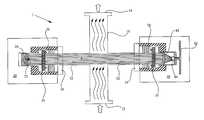
- the present inventionconstructs and arranges the IR radiation source, the sampling region, and the thermopile detector to provide a substantially linear transmission path for the IR light, as shown in FIG. 2.
- the system 1comprises a sampling region 10 , preferably a gas sampling region having a gas inlet 12 and a gas outlet 14 and constitutes a part of a flow circuitry for flow of a process gas therethrough.
- the IR radiation source 20is positioned at one side of such gas sampling region 10 .
- the IR radiation source 20comprises an IR emitter 22 and a parabolic mirror 24 , for providing a parallel beam of IR light 2 , which is transmitted along a substantially linear transmission path through the gas sampling region 10 .
- the thermopile detector 40is positioned at the other side of such gas sampling region 10 for receiving and analyzing the transmitted IR light beam.
- the thermopile detector 40comprises an IR detecting element 44 having one or more IR radiation band pass filters for selectively transmitting a portion of the IR radiation of a narrow wavelength range that encompasses the absorption wavelength that is characteristic to the IR-absorbing component(s) of interest in the process gas, so that the decrease in output signal generated by such thermopile is directly related to the amount of infrared absorption by the corresponding component(s) of interest.
- the IR light beamis focused by a focusing lens 42 before entering the IR detecting element 44 .
- thermopile detector unitmay further include a multiplicity of absorber areas, including reference (unfiltered) absorber and gas-filtered absorber regions, with the latter filters being gas-specific for sensing of the semiconductor gases or gas components of interest (e.g., arsine, phosphine, germane, stibine, distibine, silane, substituted silanes, chlorine, bromine, organometallic precursor vapor, etc.).
- reference (unfiltered) absorbere.g., arsine, phosphine, germane, stibine, distibine, silane, substituted silanes, chlorine, bromine, organometallic precursor vapor, etc.
- the gas sampling region 10is separated from the IR radiation source 20 and the thermopile detector 40 by interfacial spaces 32 and 52 , which form parts of the IR transmission path.
- the interfacial space 32is connected to the IR radiation source 20 in a sealed manner, which comprises a weld connector 34 that is detachably and sealingly connected to the IR radiation source by a spacer 35 and O-rings 36 .
- the interfacial space 52is connected to the thermopile detector 40 in a sealed manner, which comprises a weld connector 54 that is detachably and sealingly connected to the IR radiation source by a spacer 55 and O-rings 56 .
- Such weld connector 34 and 54both comprise IR transparent materials and therefore form a portion of the IR transmission path.
- the linear transmission path of the IR radiationreduces unnecessary loss of radiation intensity.
- connection between the IR source, the gas sampling region, and the thermopile detectoris simple and robust, providing a sufficient small footprint and efficient resistance against misalignment.
- an integrated circuit board 62may be positioned behind the thermopile detector 40 , for immediately receiving output signals from the thermopile detector 40 , so as to further reduce the footprint and minimize signal loss due to remote connections.
- the thermopile detector systemis utilized as an abatement tool controller for an abatement unit for treating process effluent produced in a semiconductor manufacturing operation, or other industrial process.
- the thermopile detector systemadvantageously is installed at the inlet of the abatement unit, where the abatement apparatus receives the effluent to be treated.
- the thermopile detector systemis used to sense whether or not an upstream tool that generates the effluent in active on-stream operation, is in an active operating mode, or alternatively whether or not the upstream tool is in a non-effluent-producing state, e.g., undergoing purging or cleaning.
- thermopile detector unitby way of specific example, is usefully employed as an abatement tool controller for an effluent scrubber, such as a wet/dry scrubber or a thermal scrubber, whereby the presence of the thermopile detector system transforms the scrubber into a “smart” scrubber and enhances the efficiency of the scrubber, allowing conservation of resources (lower consumables) to be achieved.
- effluent scrubbersuch as a wet/dry scrubber or a thermal scrubber
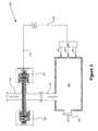
- FIG. 3shows a semiconductor process system 100 comprising a scrubber unit 140 having a gas inlet 142 and a gas outlet 144 .
- An IR source 120 and a thermopile detector 130are provided at both sides of a gas sampling region 110 near the gas inlet 142 of such scrubber unit 140 , for analyzing the composition of the effluent flowed into the scrubber.
- the output signal generated by the thermopile detector 130is forwarded through transmission line 152 to a microcontroller 150 .
- the microcontroller 150is connected to the scrubbing medium sources 160 and responsively adjusts the amount of scrubbing media (preferably fuel, water, and chemical additives) 162 , 164 , and 166 input according to the composition of the effluent as measured.
- scrubbing mediapreferably fuel, water, and chemical additives
- thermopile detector systemof the present invention.
- tetraethyloxysilanesilane, silicon tetrafluoride, silicon-containing organic compounds, boranes, arsenic hydride, phosphine, hydrogen fluoride, fluorine, tungsten hexafluoride, hydrogen chloride, chlorine, titanium tetrachloride, perfluorocarbons, nitrous oxide, ammonium, hydrogen, oxygen, argon, and helium, may be analyzed by the thermopile detector system of the present invention.
- Additional sensorssuch as temperature sensors, flow sensors, pressure transducers, ultraviolet spectrometers, mass spectrometers, and electrochemical sensors, may be provided for further measuring the flow rate, gas composition and concentration, pressure, and temperature of the effluent, so as to allow corresponding adjustment of the operational mode of the scrubber unit.
- the IR thermopile detector system of the present inventionmay be used to analyze the effluent gas species emitted from a plasma enhanced chemical vapor deposition (PECVD) chamber, in which SiO 2 films are deposited using tetraethyloxysilane (TEOS) and which performs chamber cleaning by using SiF 4 after each deposition cycle. Therefore, during the deposition cycles, the IR detector system measures the real-time concentration of TEOS in the deposition effluent. During alternating cleaning cycles, the IR detector system measures the SiF 4 concentration. Measurements obtained by the IR detector system during the alternating deposition/cleaning cycles are provided in FIG. 4. The information collected by the IR photometer can be used to adjust the settings of the downstream scrubber unit for abatement of TEOS and SiF 4 .
- PECVDplasma enhanced chemical vapor deposition
- TEOStetraethyloxysilane
- a transmission path with a smooth, reflective inner faceis provided, which minimize the absorption and dissipation of IR radiation by the surface of such transmission path.
- such inner surface of the transmission pathis characterized by a roughness in a range of from about 0.012 ⁇ m Ra to about 1.80 ⁇ m Ra, more preferably from about 0.10 ⁇ m Ra to about 0.80 ⁇ m Ra, and most preferably from about 0.10 ⁇ m Ra to about 0.20 ⁇ m Ra.
- Such inner surfacemay further be characterized by a reflectivity in a range of from about 70% to about 99%, preferably from about 92% to about 97%.
- Such smooth, reflective inner surfacemay be provided by electropolishing or super polishing techniques.
- the path length for each transmission pathis the same, and the same IR source and thermopile detector are used.
- the measurement resultsindicate that the highly polished transmission path provides much stronger signal strength than that of the moderately polished and non-polished transmission paths. provides much stronger signal strength than that of the moderately polished and non-polished transmission paths.
- Process gas that contains particles or is susceptible to particles formationmay form particle deposits along the transmission path of the IR radiation, which will absorb the IR radiation and significantly reduces the radiation intensity of the IR radiation transmitted.
- the present inventiontherefore provides a purge gas near the interfacial spaces between the gas sampling region and the IR source as well as between the gas sampling region and the thermopile detector.
- the purge gas flowprovides a sufficient force to remove the particle deposits away from the IR source and the thermopile detector, so as to prevent such particles from interfering with the detection process.
- FIG. 6shows a gas sampling region 210 having an inlet 212 and an outlet 214 for flowing a particle-containing process gas 202 therethrough.
- An IR source 220is positioned at one side of such gas sampling region 210 and is isolated therefrom by an interfacial space 232
- a thermopile detector 240is positioned at the other side of such gas sampling region 210 and is isolated therefrom by an interfacial space 252 .
- a purge gas 262is introduced into such interfacial spaces 232 and 252 from a purge gas source (not shown), preferably through a porous media 264 , for forming an uniform flow of purge gas that moves away from the IR source 220 and the thermopile detector 240 toward the gas sampling region 210 .
- a purge gas sourcenot shown
- Such flow of purge gasfurther generates vacuum at the dead-end spaces near the IR source 220 and the thermopile detector 240 , so as to force the particle deposits out of such dead-end spaces and discharge same into the process gas flow in the gas sampling region 210 .
- the purge gasmay be introduced into the interfacial spaces 232 and 252 along a direction that is substantially parallel to the process gas flow, as shown in FIG. 6, which then flows through such interfacial spaces into the gas sampling region 210 in a direction that is substantially perpendicular to the process gas flow.
- FIG. 7shows an alternative embodiment of the present invention, in which the purge gas is introduced into the interfacial spaces 332 and 352 in a direction that is substantially perpendicular to the process gas flow and flows through such interfacial spaces along the same direction into to the gas sampling region 210 .
- the purge gasmay be provided to form a gas sheath surrounding the process gas flow, so as to prevent particles from escaping from the gas sampling region.
- FIG. 8shows a purge gas 362 that forms an annular sheath 466 around the particle-containing process gas flow. Such purge gas is flowed in a direction that is confluent with the process gas flow and is therefore discharged of the gas sampling region 410 together with the process gas.
- external heating devicescan be provided for heating at least a portion of the IR transmission path (including the IR transmission windows), so as to generate a thermal gradient or heat flux, which functions to prevent the particles from accessing and depositing on the internal surface of the IR transmission path.
Landscapes
- Physics & Mathematics (AREA)
- Spectroscopy & Molecular Physics (AREA)
- General Physics & Mathematics (AREA)
- Chemical & Material Sciences (AREA)
- Biochemistry (AREA)
- Pathology (AREA)
- Health & Medical Sciences (AREA)
- Life Sciences & Earth Sciences (AREA)
- Immunology (AREA)
- Analytical Chemistry (AREA)
- General Health & Medical Sciences (AREA)
- Engineering & Computer Science (AREA)
- Power Engineering (AREA)
- Computer Hardware Design (AREA)
- Microelectronics & Electronic Packaging (AREA)
- Manufacturing & Machinery (AREA)
- Condensed Matter Physics & Semiconductors (AREA)
- Investigating Or Analysing Materials By Optical Means (AREA)
- Photometry And Measurement Of Optical Pulse Characteristics (AREA)
Abstract
Description
- This is a continuation-in-part of the U.S. patent application Ser. No. 10/623,244 for “Infrared Thermopile Detector System For Semiconductor Process Monitoring Control” filed on Jul. 18, 2003 in the name of Jose I. Arno, now pending, which is a divisional of Ser. No. 10/140,848 for “Infrared Thermopile Detector System for Semiconductor Process Monitoring and Control” filed on May 8, 2002 in the name of Jose I. Arno, now U.S. Pat. No. 6,617,175.[0001]
- This invention relates to infrared thermopile monitoring systems for semiconductor process monitoring and control.[0002]
- Most infrared energy-absorbing molecules absorb infrared radiation at discrete energy levels, so that when a gas, liquid or solid composition is exposed to infrared (IR) radiation of a broad wavelength range, the infrared energy-absorbing component(s) of that composition will absorb a portion of the IR light at very specific wavelengths. This phenomenon enables infrared-based detection, by comparing energy spectra of various known compositions with and without specific IR-absorbing component(s), to obtain an absorption profile or pattern that can be used to detect the presence of specific IR-absorbing component(s) in an unknown composition. Additionally, the concentration of the IR-absorbing component(s) in the composition directly correlates to the amount of IR light that is absorbed by such component(s), and can be determined based thereon.[0003]
- Conventional IR gas analyzers depend on grating techniques or prisms to break IR radiation into its individual wavelengths (see FIGS. 1A and 1B, showing split IR lights of wavelength λ[0004]1and λ2). The IR radiation of individual wavelengths would then be introduced into a gas cell by means of a moveable slit aperture and the IR radiation of the selected wavelength passing through the gas cell would be detected. Such dispersive IR analyzers used electronic processing means to correlate the slit aperture position with the IR energy level and the signal from the detector, and produce energy versus absorbance relations.
- The principal drawbacks of the above-described dispersive spectrometers are the loss of radiation intensity due to multiple reflection and refraction, the risk of total system failure due to misalignment of the movable parts, the cost and complexity of the spectrometer apparatus due to the number of optical components (e.g., mirrors, lens, and prism), and the space requirement for accommodating the numerous optical components used.[0005]
- Fourier transform IR (FT-IR) spectrometers, like dispersive spectrometers, also use broad energy IR sources. The originally generated IR beam is split into two beams and an interference pattern is created by sending one of the two beams in and out-of-phase, using a movable mirror. A laser beam is used to monitor the location of the movable mirror at all times. After the dual beam is sent to a sample, a sensor component of the spectrometer device receives the convoluted infrared wave pattern together with the laser-positioning beam. That information is then sent to a computer and deconvoluted using a Fourier transform algorithm. The energy versus mirror displacement data is thereby converted into energy versus absorbance relationships. Such FT-IR spectrometers suffer from similar drawbacks as described hereinabove for the conventional dispersive spectrometers.[0006]
- It is therefore an object of the present invention to provide an IR photometer system that minimizes the loss of radiation intensity during transmission of the IR radiation.[0007]
- It is another object of the present invention to provide an IR photometer system that is simple and robust, which is less vulnerable to misalignment.[0008]
- It is still another object of the present invention to provide a scrubber system for abating semiconductor process effluent, which is capable of analyzing composition of the incoming effluent and responsively modifying the operational mode accordingly.[0009]
- Other objects and advantages of the invention will be more fully apparent from the ensuing disclosure and appended claims.[0010]
- The present invention in one aspect relates to a semiconductor process system adapted for processing of a material therein, in which the system comprises:[0011]
- a sampling region for the material;[0012]
- an infrared radiation source constructed and arranged to transmit infrared radiation through the sampling region;[0013]
- a thermopile detector constructed and arranged to receive infrared radiation after the transmission thereof through the sampling region and to responsively generate output signals correlative of concentration of said material; and[0014]
- process control means arranged to receive the output signals of the thermopile detector and to responsively control one or more process conditions in and/or affecting the semiconductor process system.[0015]
- Specifically, the infrared (IR) radiation in such system of the present invention is transmitted along a transmission path that is substantially linear, while both the infrared radiation source and the thermopile detector are aligned along the transmission path of said infrared radiation. The linear transmission path for the IR radiation minimizes reflection and refraction of such IR radiation and therefore significantly reduces loss of radiation intensity during transmission. Such linear transmission path is made available by the integration of the thermopile detector, which comprises one or more radiation filters for selectively transmitting the IR radiation of a specific wavelength, therefore eliminating the requirements for monochromating the IR radiation through splitting and grating that are essential to the conventional dispersive and FT-IR spectrometers.[0016]
- The loss of IR radiation intensity can also be reduced, either independent from or in addition to the use of linear transmission path, by providing a transmission path with inner surface that is sufficient smooth and/or reflective, which minimizes absorption and dissipation of the IR radiation by such inner surface of the transmission path. Specifically, such inner surface of the transmission path is characterized by a roughness in a range of from about 0.012 μm Ra to about 1.80 μm Ra, preferably from about 0.10 μm Ra to about 0.80 μm Ra, and more preferably from about 0.10 μm Ra to about 0.20 μm Ra. Such inner surface may further be characterized by a reflectivity in a range of from about 70% to about 99%, preferably from about 92% to about 97%.[0017]
- “Ra” as used herein refers to the average differences between peaks and valleys of a surface finish.[0018]
- When the material is subjected to IR radiation in the sampling region is a process gas, such material may comprise particles or be susceptible to particle formation, resulting in deposition of particles around the IR radiation source or the thermopile detector, which may in turn significantly reduce the amount of IR radiation transmitted therethrough or completely block the transmission path.[0019]
- The present invention in such circumstances can be arranged and constructed to utilize a purge gas for purging the interfacial spaces between the sampling region containing the process gas and the IR radiation source as well as between the sampling region and the thermopile detector. Such purge gas can be passed through porous media into the interfacial spaces, to form a purge gas flow that moves any particle deposits away from the IR radiation source and the thermopile detector into the sampling region. Alternatively, particle deposit may be reduced by providing external thermal energy for heating at least a portion of the IR transmission path, so as to create a thermal gradient or heat flux that hinders the particle access to the internal surface of the transmission path.[0020]
- The semiconductor process system of the present invention may comprise a scrubber unit for abating a semiconductor process effluent from an upstream process unit, with a sampling region arranged near the inlet of such scrubber unit, so as to enable analysis of the effluent before its entry into such the scrubber unit, thereby enabling the scrubber unit to be responsively operated according the composition of the process gas.[0021]
- Other aspects, features and embodiments of the invention will be more fully apparent from the ensuing disclosure and appended claims.[0022]
- FIGS. 1A and 1B show conventional monochromator systems for splitting and grating IR radiation.[0023]
- FIG. 2 is a schematic view of a semiconductor process system comprising a linear transmission path for IR radiation, according to one embodiment of the present invention.[0024]
- FIG. 3 is a schematic view of a semiconductor process system comprising a scrubber unit having an IR radiation source and a thermopile detector constructed and arranged for analyzing an incoming process effluent near the inlet of such scrubber unit, according to one embodiment of the present invention.[0025]
- FIG. 4 is a time-concentration plot of tetraethyloxysilane (TEOS) and silicon tetrafluoride (SiF[0026]4) as measured for the process effluent from an upstream plasma enhanced chemical vapor deposition chamber that is operated according to alternative deposition and cleaning cycles.
- FIG. 5 is a graph showing the IR signal responses measured for a first transmission path having non-electropolished inner surface, a second transmission path having moderately electropolished inner surface, and a third transmission path having highly electropolished inner surface, at various IR wavelengths.[0027]
- FIGS. 6 and 7 are perspective views of semiconductor process systems comprising purge gas inlets for introducing a purge gas to remove particles from the interfacial spaces between the sampling region and the IR source as well as between the sampling region and the thermopile detector.[0028]
- FIG. 8 is a perspective view of semiconductor process system comprising purge gas inlets for forming a sheath of purge gas around the particle-containing process effluent in the sampling region.[0029]
- The present invention provides infrared thermopile detector systems useful for semiconductor process monitoring and control. U.S. patent application Ser. No. 10/140,848 filed on May 8, 2002 in the name of Jose I. Arno is incorporated herein by reference in its entirety for all purposes.[0030]
- As used herein, the term “semiconductor process” is intended to be broadly construed to include any and all processing and unit operations involved in the manufacture of semiconductor products, as well as all operations involving treatment or processing of materials used in or produced by a semiconductor manufacturing facility, as well as all operations carried out in connection with the semiconductor manufacturing facility not involving active manufacturing (examples include conditioning of process equipment, purging of chemical delivery lines in preparation for operation, etch cleaning of process tool chambers, abatement of toxic or hazardous gases from effluents produced by the semiconductor manufacturing facility, etc.).[0031]
- The thermopile-based infrared monitoring system of the invention comprises an infrared (IR) radiation source, a sampling region for exposing a material of interest (e.g., a process gas) to IR radiation, and a thermopile detector for analyzing the IR radiation as transmitted through the material of interest. The sampling region in the broad practice of the invention may comprise any suitable compartment, passageway or chamber, in which the material to be analyzed is subjected to passage of IR light therethrough for the purpose of using its IR absorbance-determined output to generate control signal(s) for process monitoring and control. The thermopile detector generates small voltages when exposed to IR light (or heat in the IR spectral regime). The output signal of the thermopile detector is proportional to the incident radiation on the detector.[0032]
- Thermopile detectors employed in the preferred practice of the present invention may have a multiple array of elements in each detector unit. For instance, in a dual element detector, one of the thermopile detector elements is used as a reference, sensing IR light in a range in which substantially no absorption occurs (e.g., wavelength of 4.00±0.02 μm). The second thermopile detector element is coated with a filter that senses IR energy in the spectral range of interest (such spectral range depending on the particular material to be monitored). Comparison of the differences in the voltages generated by the reference thermopile detector element and those generated by the thermopile detector active element(s) provides a concentration measurement. Detectors with up to 4 thermopile detector element arrays are commercially available. For example, in a 4-element detector unit, one detector element is employed as a reference and the remaining 3 detector elements are utilized for measurements in different spectral regions.[0033]
- While the ensuing disclosure is directed to a process gas as the material being subjected to IR radiation, it will be recognized that the invention is applicable to a wide variety of materials, e.g., solids, fluids (liquids and gases), multiphase materials, multicomponent materials, supercritical media, etc.[0034]
- The total loss of the IR radiation intensity (referred to herein as L[0035]Total) is determined by both the loss of IR radiation intensity caused by transmission thereof (i.e., absorption by the transmission path and the optical components, referred to herein as LPath) and the loss of IR radiation intensity due to absorption by the IR-absorbing material of interest (referred to herein as LMaterial), according to the following equations:
- LTotal=LPath+LMaterial
- The thermopile IR detector has a minimum requirement for the IR radiation intensity, in order to effectively detect such IR radiation. Therefore, when the intensity of the IR radiation generated by the IR source remains constant, the L[0036]Totalhas to be maintained at a level that is equal to or smaller than a maximum limit L0in order to enable detection of the IR radiation by the thermopile IR detector. On the other hand, since the concentration of the IR-absorbing material of interest directly correlates to and is determined by LMaterial, maximization of LMaterialwill maximize the signal strength of the measurement, which is especially important for detection and analysis of low concentration IR-absorbing materials.
- The present invention achieves the goal of maximizing L[0037]Materialwhile maintaining LTotalat or below a maximum limit L0, by reducing or minimizing LPath, according to the following methods:
- When the IR radiation is transmitted through a substantially linear transmission path from the IR source to the thermopile detector, with minimum amount of reflection and refraction therebetween, the loss of radiation intensity is effectively reduced in comparison to that of a non-linear transmission path that requires multiple reflections and refractions of the IR radiation, as shown in FIGS. 1A and 1B.[0038]
- Therefore, the present invention constructs and arranges the IR radiation source, the sampling region, and the thermopile detector to provide a substantially linear transmission path for the IR light, as shown in FIG. 2.[0039]
- Specifically, the[0040]
system 1 comprises asampling region 10, preferably a gas sampling region having agas inlet 12 and agas outlet 14 and constitutes a part of a flow circuitry for flow of a process gas therethrough. - The[0041]
IR radiation source 20 is positioned at one side of suchgas sampling region 10. Specifically, theIR radiation source 20 comprises anIR emitter 22 and aparabolic mirror 24, for providing a parallel beam ofIR light 2, which is transmitted along a substantially linear transmission path through thegas sampling region 10. - The[0042]
thermopile detector 40 is positioned at the other side of suchgas sampling region 10 for receiving and analyzing the transmitted IR light beam. Thethermopile detector 40 comprises anIR detecting element 44 having one or more IR radiation band pass filters for selectively transmitting a portion of the IR radiation of a narrow wavelength range that encompasses the absorption wavelength that is characteristic to the IR-absorbing component(s) of interest in the process gas, so that the decrease in output signal generated by such thermopile is directly related to the amount of infrared absorption by the corresponding component(s) of interest. Preferably but not necessarily, the IR light beam is focused by a focusinglens 42 before entering theIR detecting element 44. The thermopile detector unit as mentioned may further include a multiplicity of absorber areas, including reference (unfiltered) absorber and gas-filtered absorber regions, with the latter filters being gas-specific for sensing of the semiconductor gases or gas components of interest (e.g., arsine, phosphine, germane, stibine, distibine, silane, substituted silanes, chlorine, bromine, organometallic precursor vapor, etc.). - The[0043]
gas sampling region 10 is separated from theIR radiation source 20 and thethermopile detector 40 byinterfacial spaces interfacial space 32 is connected to theIR radiation source 20 in a sealed manner, which comprises aweld connector 34 that is detachably and sealingly connected to the IR radiation source by aspacer 35 and O-rings 36. Similarly, theinterfacial space 52 is connected to thethermopile detector 40 in a sealed manner, which comprises aweld connector 54 that is detachably and sealingly connected to the IR radiation source by aspacer 55 and O-rings56.Such weld connector - The linear transmission path of the IR radiation reduces unnecessary loss of radiation intensity. In addition, connection between the IR source, the gas sampling region, and the thermopile detector is simple and robust, providing a sufficient small footprint and efficient resistance against misalignment.[0044]
- Further, an[0045]
integrated circuit board 62 may be positioned behind thethermopile detector 40, for immediately receiving output signals from thethermopile detector 40, so as to further reduce the footprint and minimize signal loss due to remote connections. - In one illustrative embodiment of the invention, the thermopile detector system is utilized as an abatement tool controller for an abatement unit for treating process effluent produced in a semiconductor manufacturing operation, or other industrial process. For such purpose, the thermopile detector system advantageously is installed at the inlet of the abatement unit, where the abatement apparatus receives the effluent to be treated. In such service, the thermopile detector system is used to sense whether or not an upstream tool that generates the effluent in active on-stream operation, is in an active operating mode, or alternatively whether or not the upstream tool is in a non-effluent-producing state, e.g., undergoing purging or cleaning. The thermopile detector unit, by way of specific example, is usefully employed as an abatement tool controller for an effluent scrubber, such as a wet/dry scrubber or a thermal scrubber, whereby the presence of the thermopile detector system transforms the scrubber into a “smart” scrubber and enhances the efficiency of the scrubber, allowing conservation of resources (lower consumables) to be achieved.[0046]
- FIG. 3 shows a[0047]
semiconductor process system 100 comprising ascrubber unit 140 having a gas inlet142 and agas outlet 144. AnIR source 120 and athermopile detector 130 are provided at both sides of agas sampling region 110 near the gas inlet142 ofsuch scrubber unit 140, for analyzing the composition of the effluent flowed into the scrubber. The output signal generated by thethermopile detector 130 is forwarded throughtransmission line 152 to amicrocontroller 150. Themicrocontroller 150 is connected to the scrubbingmedium sources 160 and responsively adjusts the amount of scrubbing media (preferably fuel, water, and chemical additives)162,164, and166 input according to the composition of the effluent as measured. - Various abatable components in the effluent, including but not limited to, tetraethyloxysilane, silane, silicon tetrafluoride, silicon-containing organic compounds, boranes, arsenic hydride, phosphine, hydrogen fluoride, fluorine, tungsten hexafluoride, hydrogen chloride, chlorine, titanium tetrachloride, perfluorocarbons, nitrous oxide, ammonium, hydrogen, oxygen, argon, and helium, may be analyzed by the thermopile detector system of the present invention. Additional sensors, such as temperature sensors, flow sensors, pressure transducers, ultraviolet spectrometers, mass spectrometers, and electrochemical sensors, may be provided for further measuring the flow rate, gas composition and concentration, pressure, and temperature of the effluent, so as to allow corresponding adjustment of the operational mode of the scrubber unit.[0048]
- The IR thermopile detector system of the present invention may be used to analyze the effluent gas species emitted from a plasma enhanced chemical vapor deposition (PECVD) chamber, in which SiO[0049]2films are deposited using tetraethyloxysilane (TEOS) and which performs chamber cleaning by using SiF4after each deposition cycle. Therefore, during the deposition cycles, the IR detector system measures the real-time concentration of TEOS in the deposition effluent. During alternating cleaning cycles, the IR detector system measures the SiF4concentration. Measurements obtained by the IR detector system during the alternating deposition/cleaning cycles are provided in FIG. 4. The information collected by the IR photometer can be used to adjust the settings of the downstream scrubber unit for abatement of TEOS and SiF4.
- For further reduce the IR radiation loss (L[0050]Path) during the transmission, a transmission path with a smooth, reflective inner face is provided, which minimize the absorption and dissipation of IR radiation by the surface of such transmission path.
- When such smooth, reflective transmission path is provided, longer path length can be provided for maximizing the absorption of IR radiation by the IR-absorbing components of interest (i.e., L[0051]Gas), which is especially important for effectively measuring low concentration IR-absorbing components.
- Preferably, such inner surface of the transmission path is characterized by a roughness in a range of from about 0.012 μm Ra to about 1.80 μm Ra, more preferably from about 0.10 μm Ra to about 0.80 μm Ra, and most preferably from about 0.10 μm Ra to about 0.20 μm Ra. Such inner surface may further be characterized by a reflectivity in a range of from about 70% to about 99%, preferably from about 92% to about 97%. Such smooth, reflective inner surface may be provided by electropolishing or super polishing techniques.[0052]
- FIG. 5 shows the IR signal responses measured for a first transmission path having non-electropolished inner surface, a second transmission path having moderately electropolished inner surface, and a third transmission path having highly electropolished inner surface, at various IR wavelengths ([0053]
Channel 2=3.88 μm, Channel 4=4.65 μm, and Channel 5=4.2 μm). The path length for each transmission path is the same, and the same IR source and thermopile detector are used. The measurement results indicate that the highly polished transmission path provides much stronger signal strength than that of the moderately polished and non-polished transmission paths. provides much stronger signal strength than that of the moderately polished and non-polished transmission paths. - Process gas that contains particles or is susceptible to particles formation may form particle deposits along the transmission path of the IR radiation, which will absorb the IR radiation and significantly reduces the radiation intensity of the IR radiation transmitted.[0054]
- The present invention therefore provides a purge gas near the interfacial spaces between the gas sampling region and the IR source as well as between the gas sampling region and the thermopile detector. The purge gas flow provides a sufficient force to remove the particle deposits away from the IR source and the thermopile detector, so as to prevent such particles from interfering with the detection process.[0055]
- FIG. 6 shows a[0056]
gas sampling region 210 having aninlet 212 and anoutlet 214 for flowing a particle-containingprocess gas 202 therethrough. AnIR source 220 is positioned at one side of suchgas sampling region 210 and is isolated therefrom by aninterfacial space 232, while athermopile detector 240 is positioned at the other side of suchgas sampling region 210 and is isolated therefrom by aninterfacial space 252. Apurge gas 262 is introduced into suchinterfacial spaces porous media 264, for forming an uniform flow of purge gas that moves away from theIR source 220 and thethermopile detector 240 toward thegas sampling region 210. Such flow of purge gas further generates vacuum at the dead-end spaces near theIR source 220 and thethermopile detector 240, so as to force the particle deposits out of such dead-end spaces and discharge same into the process gas flow in thegas sampling region 210. - The purge gas may be introduced into the[0057]
interfacial spaces gas sampling region 210 in a direction that is substantially perpendicular to the process gas flow. - FIG. 7 shows an alternative embodiment of the present invention, in which the purge gas is introduced into the[0058]
interfacial spaces gas sampling region 210. - Further, the purge gas may be provided to form a gas sheath surrounding the process gas flow, so as to prevent particles from escaping from the gas sampling region. Specifically, FIG. 8 shows a[0059]
purge gas 362 that forms anannular sheath 466 around the particle-containing process gas flow. Such purge gas is flowed in a direction that is confluent with the process gas flow and is therefore discharged of thegas sampling region 410 together with the process gas. - Alternatively, external heating devices can be provided for heating at least a portion of the IR transmission path (including the IR transmission windows), so as to generate a thermal gradient or heat flux, which functions to prevent the particles from accessing and depositing on the internal surface of the IR transmission path.[0060]
- Although the invention has been variously disclosed herein with reference to illustrative embodiments and features, it will be appreciated that the embodiments and features described hereinabove are not intended to limit the invention, and that other variations, modifications and other embodiments will suggest themselves to those of ordinary skill in the art. The invention therefore is to be broadly construed, consistent with the claims hereafter set forth.[0061]
Claims (36)
Priority Applications (9)
| Application Number | Priority Date | Filing Date | Title |
|---|---|---|---|
| US10/668,489US7129519B2 (en) | 2002-05-08 | 2003-09-23 | Monitoring system comprising infrared thermopile detector |
| CNB2004800312296ACN100433267C (en) | 2003-09-23 | 2004-09-10 | Monitoring system comprising infrared thermopile detetor |
| PCT/US2004/029383WO2005034187A2 (en) | 2003-09-23 | 2004-09-10 | Monitoring system comprising infrared thermopile detector |
| EP04809711AEP1665352A4 (en) | 2003-09-23 | 2004-09-10 | CONTROL SYSTEM COMPRISING A THERMOPILE INFRARED DETECTOR |
| KR1020067007696AKR20060064689A (en) | 2003-09-23 | 2004-09-10 | Monitoring system with infrared thermopile detector |
| JP2006528035AJP2007506974A (en) | 2003-09-23 | 2004-09-10 | Surveillance system with infrared thermopile detector |
| TW093128548ATWI346993B (en) | 2003-09-23 | 2004-09-21 | Monitoring system comprising infrared thermopile detector |
| US11/555,094US7351976B2 (en) | 2002-05-08 | 2006-10-31 | Monitoring system comprising infrared thermopile detector |
| US12/060,686US7723685B2 (en) | 2002-05-08 | 2008-04-01 | Monitoring system comprising infrared thermopile detector |
Applications Claiming Priority (3)
| Application Number | Priority Date | Filing Date | Title |
|---|---|---|---|
| US10/140,848US6617175B1 (en) | 2002-05-08 | 2002-05-08 | Infrared thermopile detector system for semiconductor process monitoring and control |
| US10/623,244US7011614B2 (en) | 2002-05-08 | 2003-07-18 | Infrared thermopile detector system for semiconductor process monitoring and control |
| US10/668,489US7129519B2 (en) | 2002-05-08 | 2003-09-23 | Monitoring system comprising infrared thermopile detector |
Related Parent Applications (1)
| Application Number | Title | Priority Date | Filing Date |
|---|---|---|---|
| US10/623,244Continuation-In-PartUS7011614B2 (en) | 2002-05-08 | 2003-07-18 | Infrared thermopile detector system for semiconductor process monitoring and control |
Related Child Applications (1)
| Application Number | Title | Priority Date | Filing Date |
|---|---|---|---|
| US11/555,094ContinuationUS7351976B2 (en) | 2002-05-08 | 2006-10-31 | Monitoring system comprising infrared thermopile detector |
Publications (2)
| Publication Number | Publication Date |
|---|---|
| US20040058488A1true US20040058488A1 (en) | 2004-03-25 |
| US7129519B2 US7129519B2 (en) | 2006-10-31 |
Family
ID=34421978
Family Applications (2)
| Application Number | Title | Priority Date | Filing Date |
|---|---|---|---|
| US10/668,489Expired - LifetimeUS7129519B2 (en) | 2002-05-08 | 2003-09-23 | Monitoring system comprising infrared thermopile detector |
| US11/555,094Expired - LifetimeUS7351976B2 (en) | 2002-05-08 | 2006-10-31 | Monitoring system comprising infrared thermopile detector |
Family Applications After (1)
| Application Number | Title | Priority Date | Filing Date |
|---|---|---|---|
| US11/555,094Expired - LifetimeUS7351976B2 (en) | 2002-05-08 | 2006-10-31 | Monitoring system comprising infrared thermopile detector |
Country Status (7)
| Country | Link |
|---|---|
| US (2) | US7129519B2 (en) |
| EP (1) | EP1665352A4 (en) |
| JP (1) | JP2007506974A (en) |
| KR (1) | KR20060064689A (en) |
| CN (1) | CN100433267C (en) |
| TW (1) | TWI346993B (en) |
| WO (1) | WO2005034187A2 (en) |
Cited By (19)
| Publication number | Priority date | Publication date | Assignee | Title |
|---|---|---|---|---|
| US20040113079A1 (en)* | 2002-12-16 | 2004-06-17 | International Business Machines Corporation | Method of insitu monitoring of supercritical fluid process conditions |
| US20040113080A1 (en)* | 2002-05-08 | 2004-06-17 | Jose Arno | Infrared thermopile detector system for semiconductor process monitoring and control |
| WO2005119213A1 (en)* | 2004-06-04 | 2005-12-15 | Fraunhofer Gesellschaft Zur Förderung Der Angewandten Foschung E.V. | Device and method for optically detecting substances contained in waste gases of chemical processes |
| US20060211253A1 (en)* | 2005-03-16 | 2006-09-21 | Ing-Shin Chen | Method and apparatus for monitoring plasma conditions in an etching plasma processing facility |
| US20060217896A1 (en)* | 2003-03-28 | 2006-09-28 | Advanced Technology Materials, Inc. | Photometrically modulated delivery of reagents |
| US20070200065A1 (en)* | 2002-05-08 | 2007-08-30 | Arno Jose I | Monitoring system comprising infrared thermopile detector |
| US20080006775A1 (en)* | 2006-06-22 | 2008-01-10 | Arno Jose I | Infrared gas detection systems and methods |
| US7348538B2 (en) | 2006-02-03 | 2008-03-25 | Ge Infrastructure Sensing, Inc. | Methods and systems for detecting proximity of an object |
| US7407323B2 (en) | 2006-02-03 | 2008-08-05 | Ge Infrastructure Sensing Inc. | Methods and systems for determining temperature of an object |
| US20080213925A1 (en)* | 2003-03-28 | 2008-09-04 | Advanced Technology Materials, Inc. | Photometrically modulated delivery of reagents |
| EP1988382A3 (en)* | 2007-05-04 | 2008-12-31 | Pratt & Whitney Rocketdyne Inc. | Fuel cell instrumentation system |
| US20090246105A1 (en)* | 2008-03-25 | 2009-10-01 | Applied Materials, Inc. | Methods and apparatus for conserving electronic device manufacturing resources |
| US20100059726A1 (en)* | 2005-05-23 | 2010-03-11 | Korea Research Institute Of Bioscience And Biotechnology | Multicolor-encoded colloidal particles coated with metal nanoparticles mixture having colors in the visible region and method for preparing the same |
| US8109130B2 (en) | 2002-10-17 | 2012-02-07 | Advanced Technology Materials, Inc. | Apparatus and process for sensing fluoro species in semiconductor processing systems |
| US20150187562A1 (en)* | 2013-12-27 | 2015-07-02 | Taiwan Semiconductor Manufacturing Company Ltd. | Abatement water flow control system and operation method thereof |
| WO2017137251A1 (en)* | 2016-02-09 | 2017-08-17 | Koninklijke Philips N.V. | Particle sensor |
| US20180017485A1 (en)* | 2015-01-29 | 2018-01-18 | Panasonic Intellectual Property Management Co., Ltd. | Sensor |
| US10568726B2 (en)* | 2015-08-06 | 2020-02-25 | Transparent Materials, Llc | Photocomposite, light source and thermal detector |
| US20220404287A1 (en)* | 2021-06-17 | 2022-12-22 | Uchicago Argonne, Llc | Open aperture flow cells for on-line optical analysis of process fluids |
Families Citing this family (17)
| Publication number | Priority date | Publication date | Assignee | Title |
|---|---|---|---|---|
| US20100224264A1 (en)* | 2005-06-22 | 2010-09-09 | Advanced Technology Materials, Inc. | Apparatus and process for integrated gas blending |
| TW200846639A (en) | 2007-03-14 | 2008-12-01 | Entegris Inc | System and method for non-intrusive thermal monitor |
| JP5246395B2 (en)* | 2007-11-30 | 2013-07-24 | 大塚電子株式会社 | Optical property measuring device |
| KR101815717B1 (en) | 2009-05-29 | 2018-01-05 | 엔테그리스, 아이엔씨. | Tpir apparatus for monitoring tungsten hexafluoride processing to detect gas phase nucleation, and method and system utilizing same |
| EP2488448A1 (en)* | 2009-10-16 | 2012-08-22 | Solvay Fluor und Derivate GmbH | High-purity fluorine gas, the production and use thereof, and a method for monitoring impurities in a fluorine gas |
| TWI418969B (en) | 2010-12-01 | 2013-12-11 | Ind Tech Res Inst | Self-powered thermoelectric device for electricity consumption and related detecting method |
| DE102011004744A1 (en)* | 2011-02-25 | 2012-08-30 | Wacker Chemie Ag | Apparatus and method for determining a gas concentration in a flowing gas mixture |
| US9500583B2 (en)* | 2011-05-10 | 2016-11-22 | Li Jiang | Method and apparatus for measuring carbon dioxide dissolved in solution and wellbore monitoring systems based thereon |
| CN102538688A (en)* | 2011-12-26 | 2012-07-04 | 哈尔滨工业大学 | Infrared broadband transmission type plastic film thickness measuring device and infrared broadband transmission type plastic film thickness measuring method |
| CN102564994B (en)* | 2011-12-31 | 2014-12-24 | 聚光科技(杭州)股份有限公司 | In-place gas measurement method and in-place gas measurement device |
| JP6076800B2 (en)* | 2013-03-29 | 2017-02-08 | 三菱日立パワーシステムズ株式会社 | Laser measuring apparatus and laser measuring method |
| CN107532998B (en)* | 2015-03-09 | 2021-08-03 | 光谱传感器公司 | Intrinsically safe spectrum analyzer |
| US11085877B2 (en) | 2017-09-08 | 2021-08-10 | Schlumberger Technology Corporation | Apparatus and methods for measuring the refractive index of a fluid |
| US11009455B2 (en)* | 2018-07-31 | 2021-05-18 | Applied Materials, Inc. | Precursor delivery system and methods related thereto |
| KR102752525B1 (en)* | 2018-07-31 | 2025-01-08 | 어플라이드 머티어리얼스, 인코포레이티드 | Precursor delivery systems and related methods |
| EP3623780A1 (en)* | 2018-09-13 | 2020-03-18 | Hahn-Schickard-Gesellschaft für angewandte Forschung e.V. | Modulation of the emission intensity of an ir emitter by variation of the emitting surface |
| US12368024B2 (en)* | 2021-04-09 | 2025-07-22 | Applied Materials, Inc. | Methods and apparatus for processing a substrate |
Citations (16)
| Publication number | Priority date | Publication date | Assignee | Title |
|---|---|---|---|---|
| US4816294A (en)* | 1987-05-04 | 1989-03-28 | Midwest Research Institute | Method and apparatus for removing and preventing window deposition during photochemical vapor deposition (photo-CVD) processes |
| US4935345A (en)* | 1987-04-07 | 1990-06-19 | Arizona Board Of Regents | Implantable microelectronic biochemical sensor incorporating thin film thermopile |
| US5047352A (en)* | 1985-05-20 | 1991-09-10 | Arch Development Corporation | Selective chemical detection by energy modulation of sensors |
| US5589689A (en)* | 1994-07-07 | 1996-12-31 | Vaisala Oy | Infrared detector with Fabry-Perot interferometer |
| US5650624A (en)* | 1995-04-13 | 1997-07-22 | Engelhard Sensor Technologies, Inc. | Passive infrared analysis gas sensor |
| US5721430A (en)* | 1995-04-13 | 1998-02-24 | Engelhard Sensor Technologies Inc. | Passive and active infrared analysis gas sensors and applicable multichannel detector assembles |
| US5834777A (en)* | 1994-02-14 | 1998-11-10 | Telaire Systems, Inc. | NDIR gas sensor |
| US5962854A (en)* | 1996-06-12 | 1999-10-05 | Ishizuka Electronics Corporation | Infrared sensor and infrared detector |
| US6348650B1 (en)* | 1999-03-24 | 2002-02-19 | Ishizuka Electronics Corporation | Thermopile infrared sensor and process for producing the same |
| US6469303B1 (en)* | 2000-05-17 | 2002-10-22 | Rae Systems, Inc. | Non-dispersive infrared gas sensor |
| US20030148502A1 (en)* | 2002-02-01 | 2003-08-07 | Roland Green | Microarray synthesis instrument and method |
| US6617175B1 (en)* | 2002-05-08 | 2003-09-09 | Advanced Technology Materials, Inc. | Infrared thermopile detector system for semiconductor process monitoring and control |
| US20030175160A1 (en)* | 2002-02-14 | 2003-09-18 | Archibald William B. | High throughput screening with parallel vibrational spectroscopy |
| US20040038442A1 (en)* | 2002-08-26 | 2004-02-26 | Kinsman Larry D. | Optically interactive device packages and methods of assembly |
| US20050211555A1 (en)* | 2002-02-14 | 2005-09-29 | Solus Biosystems, Inc. | Method for multiple sample screening using IR spectroscopy |
| US7009267B2 (en)* | 2003-09-01 | 2006-03-07 | Sharp Kabushiki Kaisha | Semiconductor device |
Family Cites Families (17)
| Publication number | Priority date | Publication date | Assignee | Title |
|---|---|---|---|---|
| US4647777A (en)* | 1985-05-31 | 1987-03-03 | Ametrek, Inc. | Selective gas detector |
| JPH06317475A (en) | 1991-07-19 | 1994-11-15 | Terumo Corp | Infrared sensor and manufacturing method thereof |
| US5288649A (en) | 1991-09-30 | 1994-02-22 | Texas Instruments Incorporated | Method for forming uncooled infrared detector |
| US5282473A (en) | 1992-11-10 | 1994-02-01 | Critikon, Inc. | Sidestream infrared gas analyzer requiring small sample volumes |
| JPH0767151B2 (en) | 1993-02-25 | 1995-07-19 | 日本電気株式会社 | Infrared imaging device |
| US5549756A (en) | 1994-02-02 | 1996-08-27 | Applied Materials, Inc. | Optical pyrometer for a thin film deposition system |
| US5464983A (en) | 1994-04-05 | 1995-11-07 | Industrial Scientific Corporation | Method and apparatus for determining the concentration of a gas |
| US5874736A (en) | 1996-10-25 | 1999-02-23 | Exergen Corporation | Axillary infrared thermometer and method of use |
| NL1008665C1 (en) | 1998-03-20 | 1999-09-21 | Berkin Bv | Medium flow meter. |
| US5967992A (en) | 1998-06-03 | 1999-10-19 | Trutex, Inc. | Radiometric temperature measurement based on empirical measurements and linear functions |
| US7179653B2 (en) | 2000-03-31 | 2007-02-20 | Showa Denko K.K. | Measuring method for concentration of halogen and fluorine compound, measuring equipment thereof and manufacturing method of halogen compound |
| US6576972B1 (en) | 2000-08-24 | 2003-06-10 | Heetronix | High temperature circuit structures with expansion matched SiC, AlN and/or AlxGa1-xN(x>0.69) circuit device |
| CN1457423A (en) | 2001-03-16 | 2003-11-19 | 精工爱普生株式会社 | Infrared detection element and method for fabricating the same and equipment for measuring temperature |
| US6828172B2 (en) | 2002-02-04 | 2004-12-07 | Delphi Technologies, Inc. | Process for a monolithically-integrated micromachined sensor and circuit |
| DE60221346T2 (en)* | 2002-03-22 | 2008-04-17 | Instrumentarium Corp. | Gas analyzer using thermal sensors |
| US7129519B2 (en) | 2002-05-08 | 2006-10-31 | Advanced Technology Materials, Inc. | Monitoring system comprising infrared thermopile detector |
| JP2006275980A (en)* | 2005-03-30 | 2006-10-12 | Denso Corp | Infrared-type gas detector |
- 2003
- 2003-09-23USUS10/668,489patent/US7129519B2/ennot_activeExpired - Lifetime
- 2004
- 2004-09-10KRKR1020067007696Apatent/KR20060064689A/ennot_activeWithdrawn
- 2004-09-10CNCNB2004800312296Apatent/CN100433267C/ennot_activeExpired - Fee Related
- 2004-09-10WOPCT/US2004/029383patent/WO2005034187A2/enactiveSearch and Examination
- 2004-09-10EPEP04809711Apatent/EP1665352A4/ennot_activeWithdrawn
- 2004-09-10JPJP2006528035Apatent/JP2007506974A/ennot_activeWithdrawn
- 2004-09-21TWTW093128548Apatent/TWI346993B/ennot_activeIP Right Cessation
- 2006
- 2006-10-31USUS11/555,094patent/US7351976B2/ennot_activeExpired - Lifetime
Patent Citations (16)
| Publication number | Priority date | Publication date | Assignee | Title |
|---|---|---|---|---|
| US5047352A (en)* | 1985-05-20 | 1991-09-10 | Arch Development Corporation | Selective chemical detection by energy modulation of sensors |
| US4935345A (en)* | 1987-04-07 | 1990-06-19 | Arizona Board Of Regents | Implantable microelectronic biochemical sensor incorporating thin film thermopile |
| US4816294A (en)* | 1987-05-04 | 1989-03-28 | Midwest Research Institute | Method and apparatus for removing and preventing window deposition during photochemical vapor deposition (photo-CVD) processes |
| US5834777A (en)* | 1994-02-14 | 1998-11-10 | Telaire Systems, Inc. | NDIR gas sensor |
| US5589689A (en)* | 1994-07-07 | 1996-12-31 | Vaisala Oy | Infrared detector with Fabry-Perot interferometer |
| US5650624A (en)* | 1995-04-13 | 1997-07-22 | Engelhard Sensor Technologies, Inc. | Passive infrared analysis gas sensor |
| US5721430A (en)* | 1995-04-13 | 1998-02-24 | Engelhard Sensor Technologies Inc. | Passive and active infrared analysis gas sensors and applicable multichannel detector assembles |
| US5962854A (en)* | 1996-06-12 | 1999-10-05 | Ishizuka Electronics Corporation | Infrared sensor and infrared detector |
| US6348650B1 (en)* | 1999-03-24 | 2002-02-19 | Ishizuka Electronics Corporation | Thermopile infrared sensor and process for producing the same |
| US6469303B1 (en)* | 2000-05-17 | 2002-10-22 | Rae Systems, Inc. | Non-dispersive infrared gas sensor |
| US20030148502A1 (en)* | 2002-02-01 | 2003-08-07 | Roland Green | Microarray synthesis instrument and method |
| US20030175160A1 (en)* | 2002-02-14 | 2003-09-18 | Archibald William B. | High throughput screening with parallel vibrational spectroscopy |
| US20050211555A1 (en)* | 2002-02-14 | 2005-09-29 | Solus Biosystems, Inc. | Method for multiple sample screening using IR spectroscopy |
| US6617175B1 (en)* | 2002-05-08 | 2003-09-09 | Advanced Technology Materials, Inc. | Infrared thermopile detector system for semiconductor process monitoring and control |
| US20040038442A1 (en)* | 2002-08-26 | 2004-02-26 | Kinsman Larry D. | Optically interactive device packages and methods of assembly |
| US7009267B2 (en)* | 2003-09-01 | 2006-03-07 | Sharp Kabushiki Kaisha | Semiconductor device |
Cited By (41)
| Publication number | Priority date | Publication date | Assignee | Title |
|---|---|---|---|---|
| US20070200065A1 (en)* | 2002-05-08 | 2007-08-30 | Arno Jose I | Monitoring system comprising infrared thermopile detector |
| US20040113080A1 (en)* | 2002-05-08 | 2004-06-17 | Jose Arno | Infrared thermopile detector system for semiconductor process monitoring and control |
| US7351976B2 (en) | 2002-05-08 | 2008-04-01 | Advanced Technology Materials, Inc. | Monitoring system comprising infrared thermopile detector |
| US20060263916A1 (en)* | 2002-05-08 | 2006-11-23 | Jose Arno | Infrared thermopile detector system for semiconductor process monitoring and control |
| US7172918B2 (en) | 2002-05-08 | 2007-02-06 | Advanced Technology Materials, Inc. | Infrared thermopile detector system for semiconductor process monitoring and control |
| US8109130B2 (en) | 2002-10-17 | 2012-02-07 | Advanced Technology Materials, Inc. | Apparatus and process for sensing fluoro species in semiconductor processing systems |
| US6927393B2 (en)* | 2002-12-16 | 2005-08-09 | International Business Machines Corporation | Method of in situ monitoring of supercritical fluid process conditions |
| US20040113079A1 (en)* | 2002-12-16 | 2004-06-17 | International Business Machines Corporation | Method of insitu monitoring of supercritical fluid process conditions |
| US7711496B2 (en) | 2003-03-28 | 2010-05-04 | Advanced Technology Materials, Inc. | Photometrically modulated delivery of reagents |
| US7925450B2 (en) | 2003-03-28 | 2011-04-12 | Advanced Technology Materials, Inc. | Photometrically modulated delivery of reagents |
| US20100217415A1 (en)* | 2003-03-28 | 2010-08-26 | Advanced Technology Materials, Inc. | Photometrically modulated delivery of reagents |
| US20060217896A1 (en)* | 2003-03-28 | 2006-09-28 | Advanced Technology Materials, Inc. | Photometrically modulated delivery of reagents |
| US20080213925A1 (en)* | 2003-03-28 | 2008-09-04 | Advanced Technology Materials, Inc. | Photometrically modulated delivery of reagents |
| US7373257B2 (en) | 2003-03-28 | 2008-05-13 | Advanced Technology Materials, Inc. | Photometrically modulated delivery of reagents |
| US20080011049A1 (en)* | 2004-06-04 | 2008-01-17 | Fraunhofer-Gesellschaft Zur Forderung Der Angewandten Forschung E.V. | Device and Method for Optical Detecting Substances Contained in Waste Gases of Chemical Processes |
| US7525664B2 (en) | 2004-06-04 | 2009-04-28 | Fraunhofer-Gesellschaft zur Förderung der angewandten Forschung e.V. | Device and method for optical detecting substances contained in waste gases of chemical processes |
| WO2005119213A1 (en)* | 2004-06-04 | 2005-12-15 | Fraunhofer Gesellschaft Zur Förderung Der Angewandten Foschung E.V. | Device and method for optically detecting substances contained in waste gases of chemical processes |
| US20080134757A1 (en)* | 2005-03-16 | 2008-06-12 | Advanced Technology Materials, Inc. | Method And Apparatus For Monitoring Plasma Conditions In An Etching Plasma Processing Facility |
| US20060211253A1 (en)* | 2005-03-16 | 2006-09-21 | Ing-Shin Chen | Method and apparatus for monitoring plasma conditions in an etching plasma processing facility |
| US20100059726A1 (en)* | 2005-05-23 | 2010-03-11 | Korea Research Institute Of Bioscience And Biotechnology | Multicolor-encoded colloidal particles coated with metal nanoparticles mixture having colors in the visible region and method for preparing the same |
| US7407323B2 (en) | 2006-02-03 | 2008-08-05 | Ge Infrastructure Sensing Inc. | Methods and systems for determining temperature of an object |
| US7348538B2 (en) | 2006-02-03 | 2008-03-25 | Ge Infrastructure Sensing, Inc. | Methods and systems for detecting proximity of an object |
| US20080006775A1 (en)* | 2006-06-22 | 2008-01-10 | Arno Jose I | Infrared gas detection systems and methods |
| US20100028725A1 (en)* | 2007-05-04 | 2010-02-04 | Zillmer Andrew J | Fuel cell instrumentation system |
| EP1988382A3 (en)* | 2007-05-04 | 2008-12-31 | Pratt & Whitney Rocketdyne Inc. | Fuel cell instrumentation system |
| US7826054B2 (en) | 2007-05-04 | 2010-11-02 | Pratt & Whitney Rocketdyne, Inc. | Fuel cell instrumentation system |
| KR101612415B1 (en)* | 2008-03-25 | 2016-04-14 | 어플라이드 머티어리얼스, 인코포레이티드 | Methods and apparatus for conserving electronic device manufacturing resources |
| KR101682583B1 (en) | 2008-03-25 | 2016-12-05 | 어플라이드 머티어리얼스, 인코포레이티드 | Methods and apparatus for conserving electronic device manufacturing resources |
| US8974605B2 (en)* | 2008-03-25 | 2015-03-10 | Applied Materials, Inc. | Methods and apparatus for conserving electronic device manufacturing resources |
| US11049735B2 (en) | 2008-03-25 | 2021-06-29 | Applied Materials, Inc. | Methods and apparatus for conserving electronic device manufacturing resources |
| KR101553286B1 (en)* | 2008-03-25 | 2015-09-15 | 어플라이드 머티어리얼스, 인코포레이티드 | Methods and apparatus for conserving electronic device manufacturing resources |
| KR20160021908A (en)* | 2008-03-25 | 2016-02-26 | 어플라이드 머티어리얼스, 인코포레이티드 | Methods and apparatus for conserving electronic device manufacturing resources |
| US20090246105A1 (en)* | 2008-03-25 | 2009-10-01 | Applied Materials, Inc. | Methods and apparatus for conserving electronic device manufacturing resources |
| TWI457994B (en)* | 2008-03-25 | 2014-10-21 | Applied Materials Inc | Methods and apparatus for conserving electronic device manufacturing resources |
| US9685352B2 (en) | 2008-03-25 | 2017-06-20 | Applied Materials, Inc. | Apparatus for conserving electronic device manufacturing resources including ozone |
| US20150187562A1 (en)* | 2013-12-27 | 2015-07-02 | Taiwan Semiconductor Manufacturing Company Ltd. | Abatement water flow control system and operation method thereof |
| US20180017485A1 (en)* | 2015-01-29 | 2018-01-18 | Panasonic Intellectual Property Management Co., Ltd. | Sensor |
| US10568726B2 (en)* | 2015-08-06 | 2020-02-25 | Transparent Materials, Llc | Photocomposite, light source and thermal detector |
| WO2017137251A1 (en)* | 2016-02-09 | 2017-08-17 | Koninklijke Philips N.V. | Particle sensor |
| US20220404287A1 (en)* | 2021-06-17 | 2022-12-22 | Uchicago Argonne, Llc | Open aperture flow cells for on-line optical analysis of process fluids |
| US11933734B2 (en)* | 2021-06-17 | 2024-03-19 | Uchicago Argonne, Llc | Open aperture flow cells for on-line optical analysis of process fluids |
Also Published As
| Publication number | Publication date |
|---|---|
| EP1665352A2 (en) | 2006-06-07 |
| TW200518274A (en) | 2005-06-01 |
| EP1665352A4 (en) | 2007-09-12 |
| TWI346993B (en) | 2011-08-11 |
| KR20060064689A (en) | 2006-06-13 |
| US7351976B2 (en) | 2008-04-01 |
| US7129519B2 (en) | 2006-10-31 |
| WO2005034187A2 (en) | 2005-04-14 |
| WO2005034187A3 (en) | 2006-02-02 |
| CN1871691A (en) | 2006-11-29 |
| CN100433267C (en) | 2008-11-12 |
| JP2007506974A (en) | 2007-03-22 |
| US20070200065A1 (en) | 2007-08-30 |
Similar Documents
| Publication | Publication Date | Title |
|---|---|---|
| US7723685B2 (en) | Monitoring system comprising infrared thermopile detector | |
| US7351976B2 (en) | Monitoring system comprising infrared thermopile detector | |
| JP6450850B2 (en) | Small volume, long path length multi-pass gas cell for monitoring infrared and ultraviolet radiation | |
| EP0768525B2 (en) | Method of detecting a gas phase molecular species in the chamber effluent of a semiconductor processing chamber, and semiconductor processing system incorporating the same | |
| US5818578A (en) | Polygonal planar multipass cell, system and apparatus including same, and method of use | |
| EP1195450A2 (en) | Semiconductor processing system and method for controlling moisture level therein | |
| US6421127B1 (en) | Method and system for preventing deposition on an optical component in a spectroscopic sensor | |
| US20030098419A1 (en) | On-line UV-Visible light halogen gas analyzer for semiconductor processing effluent monitoring | |
| US20020152797A1 (en) | Gas delivery apparatus and method for monitoring a gas phase species therein | |
| KR101815717B1 (en) | Tpir apparatus for monitoring tungsten hexafluoride processing to detect gas phase nucleation, and method and system utilizing same | |
| CN1283788A (en) | Method and appts for analyzing molecular sorts in vacuum by resonant wave and spectrum sensitivity | |
| WO1999064814A1 (en) | Method and apparatus for determining processing chamber cleaning or wafer etching endpoint | |
| CN1155655A (en) | Chamber effluent monitoring system and semiconductor processing system comprising absorption spectroscopy measurement system, and method of use |
Legal Events
| Date | Code | Title | Description |
|---|---|---|---|
| AS | Assignment | Owner name:ADVANCED TECHNOLOGY MATERIALS, INC., CONNECTICUT Free format text:ASSIGNMENT OF ASSIGNORS INTEREST;ASSIGNOR:ARNO, JOSE I.;REEL/FRAME:014577/0251 Effective date:20030922 | |
| STCF | Information on status: patent grant | Free format text:PATENTED CASE | |
| FEPP | Fee payment procedure | Free format text:PAYOR NUMBER ASSIGNED (ORIGINAL EVENT CODE: ASPN); ENTITY STATUS OF PATENT OWNER: LARGE ENTITY | |
| FPAY | Fee payment | Year of fee payment:4 | |
| FPAY | Fee payment | Year of fee payment:8 | |
| AS | Assignment | Owner name:GOLDMAN SACHS BANK USA, AS COLLATERAL AGENT, NEW YORK Free format text:SECURITY INTEREST;ASSIGNORS:ENTEGRIS, INC.;POCO GRAPHITE, INC.;ATMI, INC.;AND OTHERS;REEL/FRAME:032815/0852 Effective date:20140430 Owner name:GOLDMAN SACHS BANK USA, AS COLLATERAL AGENT, NEW Y Free format text:SECURITY INTEREST;ASSIGNORS:ENTEGRIS, INC.;POCO GRAPHITE, INC.;ATMI, INC.;AND OTHERS;REEL/FRAME:032815/0852 Effective date:20140430 | |
| AS | Assignment | Owner name:GOLDMAN SACHS BANK USA, AS COLLATERAL AGENT, NEW YORK Free format text:SECURITY INTEREST;ASSIGNORS:ENTEGRIS, INC.;POCO GRAPHITE, INC.;ATMI, INC.;AND OTHERS;REEL/FRAME:032812/0192 Effective date:20140430 Owner name:GOLDMAN SACHS BANK USA, AS COLLATERAL AGENT, NEW Y Free format text:SECURITY INTEREST;ASSIGNORS:ENTEGRIS, INC.;POCO GRAPHITE, INC.;ATMI, INC.;AND OTHERS;REEL/FRAME:032812/0192 Effective date:20140430 | |
| AS | Assignment | Owner name:ENTEGRIS, INC., MASSACHUSETTS Free format text:ASSIGNMENT OF ASSIGNORS INTEREST;ASSIGNOR:ADVANCED TECHNOLOGY MATERIALS, INC.;REEL/FRAME:034894/0025 Effective date:20150204 | |
| MAFP | Maintenance fee payment | Free format text:PAYMENT OF MAINTENANCE FEE, 12TH YEAR, LARGE ENTITY (ORIGINAL EVENT CODE: M1553) Year of fee payment:12 | |
| AS | Assignment | Owner name:ADVANCED TECHNOLOGY MATERIALS, INC., CONNECTICUT Free format text:RELEASE BY SECURED PARTY;ASSIGNOR:GOLDMAN SACHS BANK USA, AS COLLATERAL AGENT;REEL/FRAME:047477/0032 Effective date:20181106 Owner name:POCO GRAPHITE, INC., MASSACHUSETTS Free format text:RELEASE BY SECURED PARTY;ASSIGNOR:GOLDMAN SACHS BANK USA, AS COLLATERAL AGENT;REEL/FRAME:047477/0032 Effective date:20181106 Owner name:ENTEGRIS, INC., MASSACHUSETTS Free format text:RELEASE BY SECURED PARTY;ASSIGNOR:GOLDMAN SACHS BANK USA, AS COLLATERAL AGENT;REEL/FRAME:047477/0032 Effective date:20181106 Owner name:ATMI, INC., CONNECTICUT Free format text:RELEASE BY SECURED PARTY;ASSIGNOR:GOLDMAN SACHS BANK USA, AS COLLATERAL AGENT;REEL/FRAME:047477/0032 Effective date:20181106 Owner name:ATMI PACKAGING, INC., CONNECTICUT Free format text:RELEASE BY SECURED PARTY;ASSIGNOR:GOLDMAN SACHS BANK USA, AS COLLATERAL AGENT;REEL/FRAME:047477/0032 Effective date:20181106 Owner name:ADVANCED TECHNOLOGY MATERIALS, INC., CONNECTICUT Free format text:RELEASE BY SECURED PARTY;ASSIGNOR:GOLDMAN SACHS BANK USA, AS COLLATERAL AGENT;REEL/FRAME:047477/0151 Effective date:20181106 Owner name:ATMI, INC., CONNECTICUT Free format text:RELEASE BY SECURED PARTY;ASSIGNOR:GOLDMAN SACHS BANK USA, AS COLLATERAL AGENT;REEL/FRAME:047477/0151 Effective date:20181106 Owner name:POCO GRAPHITE, INC., MASSACHUSETTS Free format text:RELEASE BY SECURED PARTY;ASSIGNOR:GOLDMAN SACHS BANK USA, AS COLLATERAL AGENT;REEL/FRAME:047477/0151 Effective date:20181106 Owner name:ATMI PACKAGING, INC., CONNECTICUT Free format text:RELEASE BY SECURED PARTY;ASSIGNOR:GOLDMAN SACHS BANK USA, AS COLLATERAL AGENT;REEL/FRAME:047477/0151 Effective date:20181106 Owner name:ENTEGRIS, INC., MASSACHUSETTS Free format text:RELEASE BY SECURED PARTY;ASSIGNOR:GOLDMAN SACHS BANK USA, AS COLLATERAL AGENT;REEL/FRAME:047477/0151 Effective date:20181106 | |
| AS | Assignment | Owner name:GOLDMAN SACHS BANK USA, NEW YORK Free format text:SECURITY INTEREST;ASSIGNORS:ENTEGRIS, INC.;SAES PURE GAS, INC.;REEL/FRAME:048811/0679 Effective date:20181106 | |
| AS | Assignment | Owner name:MORGAN STANLEY SENIOR FUNDING, INC., MARYLAND Free format text:ASSIGNMENT OF PATENT SECURITY INTEREST RECORDED AT REEL/FRAME 048811/0679;ASSIGNOR:GOLDMAN SACHS BANK USA;REEL/FRAME:050965/0035 Effective date:20191031 | |
| AS | Assignment | Owner name:TRUIST BANK, AS NOTES COLLATERAL AGENT, NORTH CAROLINA Free format text:SECURITY INTEREST;ASSIGNORS:ENTEGRIS, INC.;ENTEGRIS GP, INC.;POCO GRAPHITE, INC.;AND OTHERS;REEL/FRAME:060613/0072 Effective date:20220706 |