US20040057286A1 - Self-aligned split-gate NAND flash memory and fabrication process - Google Patents
Self-aligned split-gate NAND flash memory and fabrication processDownload PDFInfo
- Publication number
- US20040057286A1 US20040057286A1US10/251,664US25166402AUS2004057286A1US 20040057286 A1US20040057286 A1US 20040057286A1US 25166402 AUS25166402 AUS 25166402AUS 2004057286 A1US2004057286 A1US 2004057286A1
- Authority
- US
- United States
- Prior art keywords
- gates
- gate
- bit line
- floating
- select
- Prior art date
- Legal status (The legal status is an assumption and is not a legal conclusion. Google has not performed a legal analysis and makes no representation as to the accuracy of the status listed.)
- Granted
Links
- 238000000034methodMethods0.000titleclaimsdescription28
- 230000008569processEffects0.000titleclaimsdescription28
- 238000004519manufacturing processMethods0.000titleabstractdescription6
- 238000009792diffusion processMethods0.000claimsabstractdescription88
- 239000000758substrateSubstances0.000claimsdescription74
- 229910052710siliconInorganic materials0.000claimsdescription64
- 239000010703siliconSubstances0.000claimsdescription64
- XUIMIQQOPSSXEZ-UHFFFAOYSA-NSiliconChemical compound[Si]XUIMIQQOPSSXEZ-UHFFFAOYSA-N0.000claimsdescription63
- 230000005689Fowler Nordheim tunnelingEffects0.000claimsdescription29
- 238000002347injectionMethods0.000claimsdescription14
- 239000007924injectionSubstances0.000claimsdescription14
- 238000005530etchingMethods0.000claimsdescription12
- 230000005684electric fieldEffects0.000claimsdescription9
- 238000000151depositionMethods0.000claimsdescription6
- 230000008878couplingEffects0.000claims5
- 238000010168coupling processMethods0.000claims5
- 238000005859coupling reactionMethods0.000claims5
- 230000005012migrationEffects0.000claims1
- 238000013508migrationMethods0.000claims1
- 229910021420polycrystalline siliconInorganic materials0.000description14
- 229920005591polysiliconPolymers0.000description14
- 230000003647oxidationEffects0.000description10
- 238000007254oxidation reactionMethods0.000description10
- 150000004767nitridesChemical class0.000description9
- 239000004020conductorSubstances0.000description6
- 230000005641tunnelingEffects0.000description6
- 239000002019doping agentSubstances0.000description5
- 239000000463materialSubstances0.000description5
- ZOXJGFHDIHLPTG-UHFFFAOYSA-NBoronChemical compound[B]ZOXJGFHDIHLPTG-UHFFFAOYSA-N0.000description4
- OAICVXFJPJFONN-UHFFFAOYSA-NPhosphorusChemical compound[P]OAICVXFJPJFONN-UHFFFAOYSA-N0.000description4
- 229910052785arsenicInorganic materials0.000description4
- RQNWIZPPADIBDY-UHFFFAOYSA-Narsenic atomChemical compound[As]RQNWIZPPADIBDY-UHFFFAOYSA-N0.000description4
- 229910052796boronInorganic materials0.000description4
- 239000005380borophosphosilicate glassSubstances0.000description4
- 239000011521glassSubstances0.000description4
- 229910052698phosphorusInorganic materials0.000description4
- 239000011574phosphorusSubstances0.000description4
- 239000005360phosphosilicate glassSubstances0.000description4
- 229910021417amorphous siliconInorganic materials0.000description3
- 238000010586diagramMethods0.000description3
- 238000001312dry etchingMethods0.000description3
- 238000005468ion implantationMethods0.000description3
- 238000002955isolationMethods0.000description3
- 239000004065semiconductorSubstances0.000description3
- 230000004888barrier functionEffects0.000description2
- 230000008859changeEffects0.000description2
- 239000003989dielectric materialSubstances0.000description2
- 230000000694effectsEffects0.000description2
- 239000002784hot electronSubstances0.000description2
- 150000002500ionsChemical class0.000description2
- 229910052751metalInorganic materials0.000description2
- 239000002184metalSubstances0.000description2
- 229920002120photoresistant polymerPolymers0.000description2
- 230000015572biosynthetic processEffects0.000description1
- 238000013500data storageMethods0.000description1
- 230000008021depositionEffects0.000description1
- 238000011065in-situ storageMethods0.000description1
- 239000012212insulatorSubstances0.000description1
- 238000012986modificationMethods0.000description1
- 230000004048modificationEffects0.000description1
- 229910021421monocrystalline siliconInorganic materials0.000description1
- 150000003376siliconChemical class0.000description1
- 125000006850spacer groupChemical group0.000description1
Images


Classifications
- H—ELECTRICITY
- H10—SEMICONDUCTOR DEVICES; ELECTRIC SOLID-STATE DEVICES NOT OTHERWISE PROVIDED FOR
- H10B—ELECTRONIC MEMORY DEVICES
- H10B41/00—Electrically erasable-and-programmable ROM [EEPROM] devices comprising floating gates
- H10B41/30—Electrically erasable-and-programmable ROM [EEPROM] devices comprising floating gates characterised by the memory core region
- H10B41/35—Electrically erasable-and-programmable ROM [EEPROM] devices comprising floating gates characterised by the memory core region with a cell select transistor, e.g. NAND
- H—ELECTRICITY
- H10—SEMICONDUCTOR DEVICES; ELECTRIC SOLID-STATE DEVICES NOT OTHERWISE PROVIDED FOR
- H10B—ELECTRONIC MEMORY DEVICES
- H10B69/00—Erasable-and-programmable ROM [EPROM] devices not provided for in groups H10B41/00 - H10B63/00, e.g. ultraviolet erasable-and-programmable ROM [UVEPROM] devices
Definitions
- This inventionpertains generally to semiconductor memory devices and, more particularly, to a self-aligned split-gate NAND flash memory and process of fabricating the same.
- Nonvolatile memoryis currently available in several forms, including electrically programmable read only memory (EPROM), electrically erasable programmable read only memory (EEPROM), and flash EEPROM. Flash memory has been widely used for high volume data storage in devices such as memory cards, personal digital assistants (PDA's) and MP3 players. Such applications require high density memory, with smaller cell size and reduced cost of manufacture.
- EPROMelectrically programmable read only memory
- EEPROMelectrically erasable programmable read only memory
- flash EEPROMflash EEPROM
- Flash memoryhas been widely used for high volume data storage in devices such as memory cards, personal digital assistants (PDA's) and MP3 players. Such applications require high density memory, with smaller cell size and reduced cost of manufacture.
- stack-gateIn general, there are two basic types of nonvolatile memory cell structures: stack-gate and split-gate.
- the stack-gate memory cellusually has a floating gate and a control gate, with the control gate being positioned directly above the floating gate.
- the control gateIn a split-gate cell the control gate is still positioned above the floating gate, but it is offset laterally from it.
- the fabrication process for a stack-gate cellis generally simpler than that for a split-gate cell.
- a stack-gate cellhas an over-erase problem which a split-gate cell does not have. This problem is commonly addressed by maintaining the threshold voltage of the cell in a range of about 1.0-2.0 volts after an erase cycle, which adds complexity to the circuit design.
- split-gate memory cellAlthough a split-gate memory cell has no over-erase problem, it generally includes an additional gate known as a select gate. Such cells are typically fabricated in double-poly or triple-poly processes which involve relatively complex processing steps. In addition, split-gate cells are generally larger than stack-gate cells. Nevertheless, because of the relatively simple circuit design which is possible when there is no over-erase problem, split-gate cells are used widely, particularly in embedded nonvolatile memory applications.
- FIG. 1Cell size has also been reduced in a NAND EPROM array having a series of stack-gate flash memory cells connected in series between a bit-line and a source line, with only one bit-line contact, as illustrated in FIG. 1 and described in greater detail in U.S. Pat. Nos. 4,959,812 and 5,050,125.
- a plurality of stack-gate memory cells 21are connected in series between a bit line diffusion 22 and a source line 23 .
- the cellsare formed above a P-well 24 in a substrate 26 of either N- or P-type silicon.
- Each of the cellshas a floating gate 27 fabricated of a conductive material such as polysilicon and a control gate 28 fabricated of a conductive material such as polysilicon or polycide.
- the control gateis above and in vertical alignment with the floating gate.
- Two select gates 29 , 31are included in the array, one near the bit line contact 32 and one near source diffusion 23 .
- Diffusions 33are formed in the substrate between the stacked gates and between the stacked gates and the select gates to serve as source and drain regions for the transistors in the memory cells.
- the bit line and diffusionsare doped with N-type dopants.
- a positive voltage of about 20 voltsis applied between the P-well and the control gates, which causes electrons to tunnel from the floating gates to the channel regions beneath them.
- the floating gatesthus become positively charged, and the threshold voltage of the stack-gate cells becomes negative.
- the control gatesare biased to a level of about 20 volts positive relative to the P-well.
- the floating gatesare negatively charged, and the threshold voltage of the stack-gate cells becomes positive.
- the threshold voltage of a stack-gate cellBy changing the threshold voltage of a stack-gate cell, the channel beneath it can be in either a non-conduction state (logical “0”) or a conduction state (logical “1”) when a zero voltage is applied to the control gate during a read operation.
- Another object of the inventionis to provide a semiconductor device and process of the above character which overcome the limitations and disadvantages of the prior art.
- a self-aligned split-gate NAND flash memory cell array and method of fabricationin which a series of self-aligned split-gate cells are formed between a bit line diffusion and a common source diffusion.
- Each cellhas control and floating gates which are stacked and self-aligned with each other, and a third gate which is split from but self-aligned with the other two.
- Select gates positioned near the bit line and source diffusionsare also split from and self-aligned with the stacked control and floating gates at the ends of the series.
- the split gatesare used as erase gates, with heavily doped diffusion regions under them.
- the erase pathis from the rounded side edge of the floating gate to the corresponding erase gate, and the program path is from the channel region to the floating gate above it, with Fowler-Nordheim tunneling along both paths.
- the arrayis biased so that all of the memory cells in it can be erased simultaneously, while programming is bit selectable.
- the split gatesare used as select gates, and each of them has a channel region beneath it.
- the erase pathis from the rounded side edge of the floating gate to the corresponding select gate, with Fowler-Nordheim tunneling, and the program path is from the off-gate channel region between the floating gates to the floating gates, using hot carrier injection.
- This arrayis also biased so that all of the memory cells in it can be erased simultaneously, while programming is bit selectable.
- shallow trenchesare formed in an active region between the bit line and common source.
- the split gatesare used as select gates which extend into the trenches between adjacent control gates. These select gates have two channel regions along the side walls of the trenches and a heavily doped diffusion region near the bottom of the trench.
- the erase pathis from the rounded side edge of the floating gate to the corresponding select gate, with Fowler-Nordheim tunneling.
- the program pathis either from the channel region to the floating gate above it, with Fowler-Nordheim tunneling, or from the off-gate channel region to the floating gate near it, using hot carrier injection. This array is also biased so that all of the memory cells in the array can be erased simultaneously, while programming is bit selectable.
- FIG. 1is a cross-sectional view of a NAND flash memory array with a series of prior art stack-gate flash memory cells.
- FIG. 2is a cross-sectional view, taken along line 2 - 2 in FIG. 3, of one embodiment of a self-aligned split-gate NAND flash memory cell array incorporating the invention.
- FIG. 3is a top plan view of the embodiment of FIG. 2.
- FIGS. 4 A- 4 Hare schematic cross-sectional views illustrating the steps in one embodiment of a process for fabricating a NAND flash memory cell array in accordance with the invention.
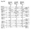
- FIGS. 5A and 5Bare circuit diagrams of a small memory array as in the embodiment of FIG. 2, showing exemplary bias conditions for erase, program and read operations.
- FIG. 6is a cross-sectional view, taken along line 6 - 6 in FIG. 7, of another embodiment of a self-aligned split-gate NAND flash memory cell array incorporating the invention.
- FIG. 7is a top plan view of the embodiment of FIG. 6.
- FIG. 8is a circuit diagram of a small memory array as in the embodiment of FIG. 6, showing exemplary bias conditions for erase, program and read operations.
- FIG. 9is a cross-sectional view, taken along line 9 - 9 in FIG. 10, of another embodiment of a self-aligned split-gate NAND flash memory cell array incorporating the invention.
- FIG. 10is a top plan view of the embodiment of FIG. 9.
- FIGS. 11 A- 11 Lare schematic cross-sectional views illustrating the steps in one embodiment of a process for fabricating the NAND flash memory cell array of FIG. 9.
- FIG. 12is a circuit diagram of a small memory array as in the embodiment of FIG. 9, showing exemplary bias conditions for erase, program and read operations.
- the memoryincludes an array of split-gate NAND flash memory cells 36 , each of which has a floating gate 37 and a control gate 38 which is positioned above and in vertical alignment with the floating gate.
- the floating gatesare fabricated of a conductive material such as polysilicon or amorphous silicon, with a preferred thickness on the order of 100 ⁇ -1000 ⁇ .
- the side edges 39 of the floating gateshave a rounded curvature, and a thin gate insulator 40 , typically a thermal oxide, is provided between each of the floating gates and the silicon substrate 41 beneath it.
- the control gatesare narrower in horizontal dimension and thicker in vertical dimension than the floating gates, with the edges of the floating gates extending laterally beyond the edges of the control gates.
- the control gatesare fabricated of a conductive material such as a doped polysilicon or polycide, and each of the control gates is insulated from the floating gate beneath it by a dielectric film 42 .
- That filmcan be either a pure oxide or a combination of oxide, nitride and oxide (ONO), and in one presently preferred embodiment, it consists of a layer nitride between two layers of oxide.
- Erase gates 43are positioned between stack-gate cells 36 , and a select gate 44 is positioned between the cell at one end of the group and bit line contact 46 .
- a second select gate 45is positioned between the cell at the other end of the group and source diffusion 51 .
- These gatesare fabricated of a conductive material such as a doped polysilicon or polycide. They are self-aligned and parallel to the adjacent control gates and floating gates, with a thick dielectric film 47 separating each erase or select gate from the adjacent control gate and a thin tunnel oxide 48 separating it from the floating gate. Both the dielectric film and the tunnel oxide can be either a pure thermal oxide or a combination of thermal oxide, a CVD oxide, and/or a CVD nitride.
- Diffusion regions 49 , a bit line diffusion 50 , and a common source diffusion 51are formed in a P-type well 52 in the upper portion of substrate 41 and doped with an N-type material. Diffusion regions 49 are positioned directly beneath the erase gates, and bit line diffusion 50 is partially overlapped by the select gate at one end of the array. Common source diffusion region 51 is partially overlapped by select gate 45 and is shared by this array of cells and by another array (not shown) of the same type.
- Erase gates 43 and select gates 44 , 45are separated from the diffusion regions and the substrate by gate oxides 53 , 54 .
- These layerscan be either a pure thermal oxide or a combination of thermal oxide and CVD oxide.
- an erase pathis formed between the rounded side edges 39 of the floating gate through tunnel oxide 48 to the adjacent erase gate 43 .
- erase gates 43 and select gates 44 , 45are parallel to the control gates 38 , which cross over the alternating floating gates 37 and isolation regions 56 in adjacent rows of cells.
- Bit lines 57are perpendicular to those gates, and cross over the bit line contact 46 , select gate 44 , control gates 38 , erase gates 43 , select gate 45 , and common source regions 51 in each row of the array.
- the memory cell array of FIGS. 2 and 3can be fabricated by the process illustrated in FIGS. 4A through 4H.
- an oxide layer 58is thermally grown to a thickness of about 70 ⁇ -150 ⁇ on a monocrystalline silicon substrate.
- the siliconis in the form of a P-type substrate 41 in which a P-type well 52 is formed.
- a P-type wellcan be formed in an N-type well in the P-type substrate.
- a conductive layer 59 of polysilicon or amorphous silicon (poly-1)is deposited on the thermal oxide to a thickness on the order of 100 ⁇ -1000 ⁇ , and a dielectric layer 61 (the inter-poly dielectric) is formed on the silicon.
- This siliconis preferably doped with phosphorus, arsenic or boron to a level on the order of 10 17 to 10 20 per cm 3 . The doping can be done in-situ during deposition of the silicon or by ion implantation directly into the silicon or through the dielectric 61 above it.
- the inter-poly dielectriccan be either a pure oxide or a combination of oxide, nitride and oxide (ONO), and in the embodiment illustrated, it consists of a lower oxide layer having a thickness on the order of 30 ⁇ -100 ⁇ , a central nitride layer having a thickness on the order of 60 ⁇ -300 ⁇ , and an upper oxide layer having a thickness on the order of 30 ⁇ -100 ⁇ .
- a second layer of polysilicon 62(poly-2) is deposited on dielectric film 61 , and is subsequently etched to form the control gates 38 .
- This layerhas a thickness on the order of 1500 ⁇ -3500 ⁇ , and is doped with phosphorus, arsenic or boron to a level on the order of 10 20 to 10 21 per cm 3 .
- a CVD oxide or nitride layer 63 having a thickness on the order of 300 ⁇ -1000 ⁇is deposited on the poly-2 layer, and is used as a mask to prevent the poly-2 material from etching away during subsequent dry etching steps.
- a photolithographic mask 64is formed over layer 63 to define the control gates, and the unmasked portions of that layer and the poly-2 layer etched away anisotropically, leaving only the portions of the poly-2 which form the control gates 38 , as illustrated in FIG. 4B.
- oxide 47is thermally grown on the side walls of the control gates to a thickness on the order of 200 ⁇ -700 ⁇ , as shown in FIG. 4C.
- the exposed portions of the inter-poly dielectric 61 and the underlying portions of the poly-1 layer 59are etched away anisotropically to form the floating gates, with only a thin layer of oxide 58 being left on the surface of substrate between the gates, as illustrated in FIG. 4D.
- Diffusion regions 49are then formed in the substrate between the gates by ion implantation, using dopants such as P 31 or As 75 , as illustrated in FIG. 4D.
- gate oxide 54for the select gate, tunnel oxide 48 , thermal oxide 53 on diffusion regions 49 , and the oxide 47 surrounding the poly-2 control gates, as shown in FIG. 4E.
- Gate oxide 54is thus built up to a thickness on the order of 100 ⁇ -400 ⁇
- tunnel oxide 48is built up to a thickness on the order of 100 ⁇ -300 ⁇ .
- a thin CVD oxide of about 50 ⁇ -200 ⁇can be deposited before or after thermal oxidation.
- the side edges 39 of floating gates 37become rounded because the oxidation rate of the polysilicon is faster near the interface between it and the dielectric materials above and below it.
- the rounded curvatureresults in an electric field enhancement which facilitates electron tunneling from the floating gates to the erase gates.
- the rounding of the side edgeseliminates the localized trapping effect that occurs in the tunnel oxide near the square corners of a floating gate when a cell operates in erase mode and the electrons tunnel from the floating gate to the erase gate.
- the rounded edgesenhance the program-and-erase performance of the memory cells.
- each of the control gatesis self-aligned to the floating gate beneath it, and the control gate is narrower than the floating gate. Therefore, the edges of the floating gate extend laterally beyond the edges of the control gate.
- a conductive layer (poly-3) 65is deposited over the entire wafer, as illustrated in FIG. 4E.
- This layeris typically doped polysilicon or polycide, and it is deposited to a thickness on the order of 1500 ⁇ -4000 ⁇ .
- the poly-3 layeris then etched anisotropically, leaving only the portions of it which form erase gates 43 and select gates 44 , 45 , as illustrated in FIG. 4F. Being formed in this manner, the erase gates and the select gate are self-aligned and parallel to the control gates.
- N-type dopantssuch as P 31 or As 75 are implanted into P-well 52 to form bit line diffusion 50 and common source diffusion 51 , as illustrated in FIG. 4G.
- a glass material 66such as phosphosilicate glass (PSG) or borophosphosilicate glass (BPSG) is deposited across the entire wafer, then etched for bit line contacts 46 . Finally, a metal layer is deposited over the glass and patterned to form bit lines 57 and bit line contacts 46 .
- PSGphosphosilicate glass
- BPSGborophosphosilicate glass
- FIGS. 5A and 5Bexemplary bias voltages for erase (ERS), program (PGM) and read (RD) operations are shown next to the terminals of the array.
- memory cell C 1 nis selected. This cell is located at the intersection of control gate CG 1 and bit line BLn, and is encircled on the drawing for ease of location. All of the other memory cells in the array are unselected.
- the voltage required for Fowler-Nordheim tunnelingis reduced by the resulting enhancement in the effective electric field.
- the enhanced fieldalso makes it possible to use a thicker tunnel oxide while still maintaining sufficient electron tunneling.
- Erasingcan be done using two different bias conditions.
- the control gate of memory cellIn the first erase mode, the control gate of memory cell is biased at a level on the order of ⁇ 7 to ⁇ 12 volts, the erase gate is biased to a level on the order of 3-7 volts, the bit line is kept floating, and the select gates are maintained at 0 volts.
- the control gate of the memory cellIn the second erase mode, the control gate of the memory cell is biased at 0 volts, the erase gate is biased to a level on the order of 9-12 volts, the bit line is kept floating, and the common source, select gates and P-well are all biased at 0 volts.
- Fowler-Nordheim tunnelingcauses electrons to tunnel from the channel region to the floating gate above it, and the floating gate becomes negatively charged.
- a bias of 15-18 voltsis applied to the control gate of the selected memory cell C 1n
- 1-3 voltsis applied to the select gate SG 0
- erase gates EG 0 -EG 14 , select gate SG 1 bit line 57 , and common source 51are maintained at 0 volts.
- the floating gateis negatively charged, the threshold voltage of the memory cell, which preferably is on the order of 1-3 volts, becomes higher.
- the memory cellis turned off when the control gate is biased at 0 volts during a read operation.
- the memory cellgoes into a non-conductive state (logic “0”).
- the bit lineis biased at 5-8 volts, and the control gate is biased at 15-18 volts. This results in negligible Fowler Nordheim tunneling, and the floating gate charges remain unchanged.
- the other unselected memory cells C 0n and C 2nare biased with 0 volts on the bit line and 6-8 volts on the control gate. This also minimizes Fowler-Nordheim tunneling, and the charges on the floating gates do not change.
- FIG. 5BAnother set of bias conditions for the program mode is illustrated in FIG. 5B.
- the selected memory cell C 1nis biased with 10-13 volts on the control gate, 0 volts on select gate SG 0 , the erase gates, and the common source, and ⁇ 5 volts on select gate SG 1 , the bit line, and the P-well.
- the cell biased in this mannermost of the applied voltage falls across the gate oxide beneath the floating gate. That results in Fowler-Nordheim tunneling which causes electrons to migrate from the channel region to the floating gate.
- the selected memory cell C 1nis biased with 0 volts on the control gate, source and erase gates, 1-3 volts on the bit line, and Vcc on the select gates.
- the unselected memory cells in the bit line directione.g. C 0n and C 2n are turned on by applying 5-8 volts to the control gates.
- the memory cellWhen the memory cell is erased, it shows a conductive state because the channel of selected cell is turned on and the select transistors and the other cells in the same bit line direction are also turned on. Thus, a logic “1” is returned by the sense amplifier.
- the memory cellWhen the memory cell is programmed, it shows a non-conductive state because the channel of the selected cell is turned off. Thus, a logic “0” is returned by the sense amplifier.
- the unselected memory cells C 1(n ⁇ 1) and C 1(n+1)both the bit line and the common source are biased at 0 volts, and no current flows between the bit line and the source.
- FIGS. 6 and 7is generally similar to the embodiment of FIGS. 2 and 3, and like reference numerals designate corresponding elements in the two embodiments.
- select gates 71are positioned between the control and floating gate stacks, and there are no diffusions in the substrate beneath the select gates.
- the select gatesare formed in the same manner as erase gates 43 in the embodiment of FIG. 2, and they are thus self-aligned with the stacked control and floating gates.
- the erase pathis from the rounded side edges 39 of the floating gate through tunnel oxide 48 to the adjacent select gate 71 .
- select gates 44 , 45 and 71are parallel to the control gates 38 , which cross over the alternating floating gates 37 and isolation regions 56 in adjacent rows of cells.
- Bit lines 57are perpendicular to the select and control gates, and cross over the bit line contact 46 , select gates 44 , 45 and 71 , control gates 38 , and common source regions 51 in each row of the array.
- FIGS. 6 and 7Operation and use of the embodiment of FIGS. 6 and 7 can be described with reference to FIG. 8 where exemplary bias voltages for erase (ERS), program (PGM) and read (RD) operations are shown next to the terminals of the array.
- ERSerase
- PGMprogram
- RDread
- memory cell C 1 nis once again assumed to be selected. This cell is located at the intersection of control gate CG 1 and bit line BLn, and is encircled on the drawing for ease of location. All of the other memory cells in the array are unselected.
- Erasingcan be done with either of two different bias conditions.
- the control gate of the memory cellis biased at ⁇ 7 to ⁇ 12 volts
- select gates SG 1 -SG 15are biased at 3-7 volts
- select gates SG 0 and SG 16are biased either at 0 volts or at 3-7 volts
- the bit lineis floating
- the common sourceis biased at 0 volts.
- the control gate, P-well and common sourceare biased at 0 volts
- select gates SG 1 -SG 15are biased at 9-12 volts
- select gates SG 0 and SG 16are biased either at 0 volts or at 9-12 volts
- the bit lineis floating.
- the control gate of the selected memory cell C 1nis biased to a level of 10-12 volts, 7-9 volts is applied to select gates SG 0 , SG 2 -SG 16 and to the control gates of the other memory cells in the same bit line direction as the selected cell (e.g. C 0n and C 2n ), the bit line is held at 0 volts, and 6-8 volts is applied to the common source.
- the cells and the select transistorsare turned on by applying 7-9 volts to the control gates and to the select gates.
- the voltage applied to the select gate just before the selected cellcan be on the low side, preferably on the order of 1-2 volts.
- the floating gateis negatively charged, the threshold voltage of the memory cell, which preferably is on the order of 1-3 volts, becomes higher.
- the memory cellis turned off when the control gate is biased at 0 volts during a read operation.
- the memory cellgoes into a non-conductive state (logic “0”).
- the bit lineis biased at 3 volts
- the select gate SG 1is at 1-2 volts
- the control gateis at 10-12 volts.
- select transistors S 1(n ⁇ 1) and S 1(n+1)are turned off, and there is no mid-channel hot carrier injection takes in cells C 1(n ⁇ 1) and C 1(n+1).
- the other unselected memory cells C 0n and C 2nare biased with 0 volts to the bit line and 7-9 volts to the control gate, which minimizes the mid-channel hot carrier injection, and the floating gate charges are unchanged.
- the control gate of the selected memory cell C 1n and the common sourceare biased to 0 volts, 1-3 volts is applied to the bit line, and Vcc is applied to the select gates.
- the unselected memory cells in the bit line directione.g. C On and C 2n , are turned on by applying 5-8 volts to their control gates.
- the readshows a conductive state because the channel of selected cell is turned on, and the other cells and the select transistors in the same bit line direction also turned on. Thus, a logic “1” is returned by the sense amplifier.
- the readshows a non-conductive state because the channel of the selected cell is turned off, and hence the sense amplifier returns a logic “0”.
- the unselected memory cells C 1(n ⁇ 1) and C 1(n+1)both the bit line and common source nodes are biased at 0 volts, and there is no current flow between the bit line and the common source nodes.
- FIGS. 9 and 10Another embodiment of a NAND cell array incorporating the invention is illustrated in FIGS. 9 and 10. To the extent that this embodiment is similar to that of FIGS. 6 - 7 , like reference numerals designate corresponding elements in the two embodiments.
- a plurality of shallow trenches 74are formed in the active region between bit line diffusion 50 and common source diffusion 51 .
- Select gates 76extend into the trenches, and are separated from the silicon substrate by a thick gate dielectric film 77 , which can be either a pure thermal oxide or a combination of thermal oxide and CVD oxide.
- the select gatesare formed of a conductive material such as doped polysilicon or polycide, and they are self-aligned with the control gates and floating gates in the adjacent cells.
- Each of the select gates 76has two channel regions along the side walls of the trench and a heavily doped diffusion region near the bottom of the trench.
- Source diffusions 78are formed in the substrate beneath the select gates and doped with the dopants of opposite type to the silicon substrate.
- the erase path in this embodimentis from the rounded side edges 39 of the floating gates through the tunnel oxide to the select gates.
- select gates 44 , 45 and 76are parallel to control gates 38 , which cross over the alternating floating gates 37 and isolation regions 56 in adjacent rows of cells.
- Bit lines 57are perpendicular to the select and control gates, and cross over the bit line contact 46 , select gates 44 , 45 and 76 , control gates 38 , and common source regions 51 in each row of the array.
- the memory cell array of FIGS. 9 and 10can be fabricated by the process illustrated in FIGS. 11 A- 11 L.
- an oxide layer 58is thermally grown on the silicon substrate to a thickness of about 70 ⁇ -150 ⁇ , and a conductive layer 59 of polysilicon or amorphous silicon (poly-1) is deposited on the thermal oxide to a thickness on the order of 100 ⁇ -1000 ⁇ , and a dielectric layer 61 is formed on the silicon.
- the poly-1is preferably doped with phosphorus, arsenic or boron to a level on the order of 10 17 to 10 20 per cm 3 .
- a dielectric film 61(the inter-poly dielectric) is formed on the poly-1 layer.
- This filmcan be either a pure oxide or a combination of oxide and nitride, e.g. a layer of nitride between two layers of oxide (ONO) as in the embodiment of FIGS. 4 A- 4 H.
- a second layer of polysilicon 62(poly-2) is deposited on dielectric film 61 , and is subsequently etched to form the control gates 38 .
- This layerhas a thickness on the order of 1500 ⁇ -3500 ⁇ , and is doped with phosphorus, arsenic or boron to a level on the order of 10 20 to 10 21 per cm 3 .
- a CVD oxide or nitride layer 63 having a thickness on the order of 300 ⁇ -1000 ⁇is deposited on the poly-2 layer, and is used as a mask to prevent the poly-2 material from etching away during subsequent dry etching steps.
- a photolithographic mask 64is formed over layer 63 to define the control gates, and the unmasked portions of that layer and the poly-2 layer etched away anisotropically, leaving only the portions of the poly-2 which form the control gates 38 , as illustrated in FIG. 11B.
- oxide 47is thermally grown on the side walls of the control gates to a thickness on the order of 200 ⁇ -700 ⁇ , as shown in FIG. 11C.
- the exposed portions of the inter-poly dielectric 61 and the underlying portions of the poly-1 layer 59 and oxide layer 58are etched away anisotropically, as illustrated in FIG. 11D. Further anisotropic dry etching results in the formation of trenches 74 in the upper portion of the silicon substrate, as illustrated in FIG. 11E.
- a CVD oxide 79is deposited across the wafer, as shown in FIG. 11F, then etched anisotropically to leave oxide spacers 81 along the side walls of the control gates and trenches as shown in FIG. 11G. Ions are then implanted through the bottom walls of the trenches to form source regions 78 , as illustrated in FIG. 11G.
- Gate oxide 54is thus built up to a thickness on the order of 100 ⁇ -400 ⁇
- tunnel oxide 48is built up to a thickness on the order of 100 ⁇ -300 ⁇ .
- a thin CVD oxide of about 50 ⁇ -200 ⁇can be deposited before or after thermal oxidation.
- the side edges 39 of floating gates 37become rounded because the oxidation rate of the polysilicon is faster near the interface between it and the dielectric materials above and below it.
- the rounded curvatureresults in an electric field enhancement which facilitates electron tunneling from the floating gates to the erase gates.
- the rounding of the side edgeseliminates the localized trapping effect that occurs in the tunnel oxide near the square corners of a floating gate when a cell operates in erase mode and the electrons tunnel from the floating gate to the select gate.
- the rounded edgesenhance the program-and-erase performance of the memory cells.
- each of the control gatesis self-aligned to the floating gate beneath it, the control gate is narrower than the floating gate, and the edges of the floating gate extend laterally beyond the edges of the control gate.
- a conductive layer (poly-3) 65is deposited into the trenches and over the entire wafer, as illustrated in FIG. 11I.
- This layeris typically doped polysilicon or polycide, and it is deposited to a thickness on the order of 1500 ⁇ -4000 ⁇ above the dielectric film 47 overlying the control gates.
- the poly-3 layeris then etched anisotropically, leaving only the portions of it which form select gates 44 , 45 and 76 , as illustrated in FIG. 11J. Being formed in this manner, the select gates are self-aligned and parallel to the control gates.
- N-type dopantssuch as P 31 or As 75 are implanted into the substrate to form the bit line diffusion 50 and common source diffusion 51 , as illustrated in FIG. 11K.
- a glass materialsuch as phosphosilicate glass (PSG) or borophosphosilicate glass (BPSG) is deposited across the entire wafer, then etched for bit line contacts 46 . Finally, a metal layer is deposited over the glass and patterned to form bit lines 57 and bit line contacts 46 .
- PSGphosphosilicate glass
- BPSGborophosphosilicate glass
- FIG. 9Operation and use of the embodiment of FIG. 9 can be described with reference to FIGS. 12 A- 12 C where exemplary bias voltages for erase (ERS), program (PGM) and read (RD) operations are shown next to the terminals of the memory cell array.
- memory cell C 1nis selected. This cell is located at the intersection of control gate CG 1 and bit line BLn, and is encircled on the drawing for ease of location. All of the other memory cells in the array are unselected.
- Erasingcan be done with either of two different bias conditions.
- the control gate of the memory cellis biased at ⁇ 7 to ⁇ 12 volts
- select gates SG 1 -SG 15are biased at 3-7 volts
- select gates SG 0 and SG 16are biased either at 0 volts or at 3-7 volts
- the bit lineis floating
- the common sourceis biased at 0 volts.
- the control gate, P-well and common source of the memory cellare biased at 0 volts
- select gates SG 1 -SG 15are biased at 9-12 volts
- select gates SG 0 and SG 16are biased either at 0 volts or at 9-12 volts
- the bit lineis floating.
- the control gate of the selected memory cell C 1nis biased to a level of 15-18 volts, 6-9 volts is applied to select gates SG 0 -SG 15 , and the bit line, select gate SG 16 , and the common source are maintained at 0 volts.
- select gates SG 0 -SG 15the bit line, select gate SG 16 , and the common source are maintained at 0 volts.
- the floating gateis negatively charged, and the threshold voltage of the memory cell, which preferably is on the order of 1-3 volts, becomes higher. Therefore, the memory cell is turned off when the control gate is biased at 0 volts during a read operation. Following a program operation, the memory cell goes into a non-conductive state (logic “0”).
- the bit lineis biased at 5-8 volts, and the control gate is biased at 15-18 volts. This results in negligible Fowler Nordheim tunneling, and the floating gate charges remain unchanged.
- the other unselected memory cells C 0n and C 2nare biased with 0 volts on the bit line and 6-8 volts on the control gate. This also minimizes Fowler-Nordheim tunneling, and the charges on the floating gates do not change.
- FIG. 12BAnother set of bias conditions for the program mode is illustrated in FIG. 12B.
- the selected memory cell C 1nis biased with 10-13 volts on the control gate, 1-3 volts on select gates SG 0 -SG 15 , ⁇ 5 volts on select gate SG 16 , the bit line and P-well, and 0 volts on the common source.
- the cell biased in this mannermost of the applied voltage falls across the gate oxide beneath the floating gate. That results in Fowler-Nordheim tunneling which causes electrons to migrate from the channel region to the floating gate.
- FIG. 12Cillustrates a third set of bias conditions for the program mode, in which 10-12 volts is applied to the control gate of the selected memory cell C 1n , 7-9 volts is applied to select gates SG 0 and, SG 2 -SG 16 and to the control gates of other memory cells in the same bit line direction as the selected cell (e.g. C 0n and C 2n ), the bit line is maintained at 0 volts, and 6-8 volts is applied to the common source.
- the cells and the select transistorsare turned on by applying 7-9 volts to the control gates and select gates.
- the voltage applied to the select gate (SG 1 in this example) just before the selected cell (C 1n in this example)can be on the low side, preferably on the order of 1-2 volts.
- the floating gateis negatively charged, the threshold voltage of the memory cell, which preferably is on the order of 1-3 volts, becomes higher.
- the memory cellis turned off when the control gate is biased at 0 volts during a read operation.
- the memory cellgoes into a non-conductive state (logic “0”).
- the bit lineis biased at 3 volts
- the select gate SG 1is at 1-2 volts
- the control gateis at 10-12 volts.
- select transistors S 1(n ⁇ 1) and S 1(n+1)are turned off, and there is no mid-channel hot carrier injection takes in cells C 1(n ⁇ 1) and C 1(n+1) .
- the other unselected memory cells C 0n and C 2nare biased with 0 volts to the bit line and 7-9 volts to the control gate, which minimizes the mid-channel hot carrier injection, and the floating gate charges are unchanged.
- the control gate of the selected memory cell C 1n and the sourceare biased to 0 volts, 1-3 volts is applied to the bit line, and Vcc is applied to the select gates.
- the unselected memory cells in the bit line directione.g. C 0n and C 2n , are turned on by applying 5-8 volts to their control gates.
- the readshows a conductive state because the channel of selected cell is turned on, and the other cells and the select transistors in the same bit line direction also turned on. Thus, a logic “1” is returned by the sense amplifier.
- the readshows a non-conductive state because the channel of the selected cell is turned off, and hence the sense amplifier returns a logic “0”.
- the unselected memory cells C 1(n ⁇ 1) and C 1(n+1)both the bit line and common source nodes are biased at 0 volts, and there is no current flow between the bit line and the common source nodes.
- the inventionhas a number of important features and advantages. It provides a self-aligned split-gate NAND flash memory cell array which has significantly smaller cell size and greater cell density than memory structures heretofore provided.
- the arraycomprises a plurality of self-aligned split cells between a bit line diffusion and a common source diffusion. Each cell has control and floating gates which are stacked and self-aligned with each other, and a third gate which is split from but self-aligned with the other two.
- the split gatesare used as erase gates, with heavily doped diffusion regions under them.
- the erase pathis from the rounded side edge of the floating gate to the corresponding erase gate
- the program pathis from the channel region to the floating gate above it, with Fowler-Nordheim tunneling along both paths.
- the arrayis biased so that all of the memory cells in it can be erased simultaneously, while programming is bit selectable. As noted above, the size of the memory cells is greatly reduced with this structure.
- the split gatesare used as select gates, and each of them has a channel region beneath it.
- the erase pathis from the rounded side edge of the floating gate to the corresponding select gate, with Fowler-Nordheim tunneling, and the program path is from the off-gate channel region between the floating gates to the floating gates, using hot carrier injection.
- This arrayis also biased so that all of the memory cells in it can be erased simultaneously, while programming is bit selectable.
- the size of the memory cellsis greatly reduced with this structure.
- shallow trenchesare formed in the active region between the bit line and common source.
- the split gatesare used as select gates which extend into the trenches between adjacent control gates. These select gates have two channel regions along the side walls of the trenches and a heavily doped diffusion region near the bottom of the trench.
- the erase pathis from the rounded side edge of the floating gate to the corresponding select gate, with Fowler-Nordheim tunneling.
- the program pathis either from the channel region to the floating gate above it, with Fowler-Nordheim tunneling, or from the off-gate channel region to the floating gate near it, using hot carrier injection.
- This arrayis also biased so that all of the memory cells in the array can be erased simultaneously, while programming is bit selectable. The size of the memory cells is also greatly reduced with this structure.
Landscapes
- Non-Volatile Memory (AREA)
- Semiconductor Memories (AREA)
Abstract
Description
- 1. Field of Invention[0001]
- This invention pertains generally to semiconductor memory devices and, more particularly, to a self-aligned split-gate NAND flash memory and process of fabricating the same.[0002]
- 2. Related Art[0003]
- Nonvolatile memory is currently available in several forms, including electrically programmable read only memory (EPROM), electrically erasable programmable read only memory (EEPROM), and flash EEPROM. Flash memory has been widely used for high volume data storage in devices such as memory cards, personal digital assistants (PDA's) and MP3 players. Such applications require high density memory, with smaller cell size and reduced cost of manufacture.[0004]
- In general, there are two basic types of nonvolatile memory cell structures: stack-gate and split-gate. The stack-gate memory cell usually has a floating gate and a control gate, with the control gate being positioned directly above the floating gate. In a split-gate cell the control gate is still positioned above the floating gate, but it is offset laterally from it. The fabrication process for a stack-gate cell is generally simpler than that for a split-gate cell. However, a stack-gate cell has an over-erase problem which a split-gate cell does not have. This problem is commonly addressed by maintaining the threshold voltage of the cell in a range of about 1.0-2.0 volts after an erase cycle, which adds complexity to the circuit design. Although a split-gate memory cell has no over-erase problem, it generally includes an additional gate known as a select gate. Such cells are typically fabricated in double-poly or triple-poly processes which involve relatively complex processing steps. In addition, split-gate cells are generally larger than stack-gate cells. Nevertheless, because of the relatively simple circuit design which is possible when there is no over-erase problem, split-gate cells are used widely, particularly in embedded nonvolatile memory applications.[0005]
- A split-gate memory cell of relatively small size, with efficient erase performance and a small programming current is described in U.S. Pat. Nos. 6,091,104 and 6,291,297.[0006]
- Cell size has also been reduced in a NAND EPROM array having a series of stack-gate flash memory cells connected in series between a bit-line and a source line, with only one bit-line contact, as illustrated in FIG. 1 and described in greater detail in U.S. Pat. Nos. 4,959,812 and 5,050,125. In this array, a plurality of[0007]
stack-gate memory cells 21 are connected in series between abit line diffusion 22 and asource line 23. The cells are formed above a P-well 24 in asubstrate 26 of either N- or P-type silicon. Each of the cells has afloating gate 27 fabricated of a conductive material such as polysilicon and acontrol gate 28 fabricated of a conductive material such as polysilicon or polycide. The control gate is above and in vertical alignment with the floating gate. - Two[0008]
select gates bit line contact 32 and onenear source diffusion 23.Diffusions 33 are formed in the substrate between the stacked gates and between the stacked gates and the select gates to serve as source and drain regions for the transistors in the memory cells. The bit line and diffusions are doped with N-type dopants. - To erase the memory cell, a positive voltage of about 20 volts is applied between the P-well and the control gates, which causes electrons to tunnel from the floating gates to the channel regions beneath them. The floating gates thus become positively charged, and the threshold voltage of the stack-gate cells becomes negative.[0009]
- To program the memory cells, the control gates are biased to a level of about 20 volts positive relative to the P-well. As electrons tunnel from the channel region to the floating gates, the floating gates are negatively charged, and the threshold voltage of the stack-gate cells becomes positive. By changing the threshold voltage of a stack-gate cell, the channel beneath it can be in either a non-conduction state (logical “0”) or a conduction state (logical “1”) when a zero voltage is applied to the control gate during a read operation.[0010]
- It is in general an object of the invention to provide a new and improved semiconductor device and process for fabricating the same.[0011]
- Another object of the invention is to provide a semiconductor device and process of the above character which overcome the limitations and disadvantages of the prior art.[0012]
- These and other objects are achieved in accordance with the invention by providing a self-aligned split-gate NAND flash memory cell array and method of fabrication in which a series of self-aligned split-gate cells are formed between a bit line diffusion and a common source diffusion. Each cell has control and floating gates which are stacked and self-aligned with each other, and a third gate which is split from but self-aligned with the other two. Select gates positioned near the bit line and source diffusions are also split from and self-aligned with the stacked control and floating gates at the ends of the series.[0013]
- In one disclosed embodiment, the split gates are used as erase gates, with heavily doped diffusion regions under them. The erase path is from the rounded side edge of the floating gate to the corresponding erase gate, and the program path is from the channel region to the floating gate above it, with Fowler-Nordheim tunneling along both paths. The array is biased so that all of the memory cells in it can be erased simultaneously, while programming is bit selectable.[0014]
- In a second disclosed embodiment, the split gates are used as select gates, and each of them has a channel region beneath it. The erase path is from the rounded side edge of the floating gate to the corresponding select gate, with Fowler-Nordheim tunneling, and the program path is from the off-gate channel region between the floating gates to the floating gates, using hot carrier injection. This array is also biased so that all of the memory cells in it can be erased simultaneously, while programming is bit selectable.[0015]
- In a third disclosed embodiment, shallow trenches are formed in an active region between the bit line and common source. The split gates are used as select gates which extend into the trenches between adjacent control gates. These select gates have two channel regions along the side walls of the trenches and a heavily doped diffusion region near the bottom of the trench. The erase path is from the rounded side edge of the floating gate to the corresponding select gate, with Fowler-Nordheim tunneling. The program path is either from the channel region to the floating gate above it, with Fowler-Nordheim tunneling, or from the off-gate channel region to the floating gate near it, using hot carrier injection. This array is also biased so that all of the memory cells in the array can be erased simultaneously, while programming is bit selectable.[0016]
- FIG. 1 is a cross-sectional view of a NAND flash memory array with a series of prior art stack-gate flash memory cells.[0017]
- FIG. 2 is a cross-sectional view, taken along line[0018]2-2 in FIG. 3, of one embodiment of a self-aligned split-gate NAND flash memory cell array incorporating the invention.
- FIG. 3 is a top plan view of the embodiment of FIG. 2.[0019]
- FIGS.[0020]4A-4H are schematic cross-sectional views illustrating the steps in one embodiment of a process for fabricating a NAND flash memory cell array in accordance with the invention.
- FIGS. 5A and 5B are circuit diagrams of a small memory array as in the embodiment of FIG. 2, showing exemplary bias conditions for erase, program and read operations.[0021]
- FIG. 6 is a cross-sectional view, taken along line[0022]6-6 in FIG. 7, of another embodiment of a self-aligned split-gate NAND flash memory cell array incorporating the invention.
- FIG. 7 is a top plan view of the embodiment of FIG. 6.[0023]
- FIG. 8 is a circuit diagram of a small memory array as in the embodiment of FIG. 6, showing exemplary bias conditions for erase, program and read operations.[0024]
- FIG. 9 is a cross-sectional view, taken along line[0025]9-9 in FIG. 10, of another embodiment of a self-aligned split-gate NAND flash memory cell array incorporating the invention.
- FIG. 10 is a top plan view of the embodiment of FIG. 9.[0026]
- FIGS.[0027]11A-11L are schematic cross-sectional views illustrating the steps in one embodiment of a process for fabricating the NAND flash memory cell array of FIG. 9.
- FIG. 12 is a circuit diagram of a small memory array as in the embodiment of FIG. 9, showing exemplary bias conditions for erase, program and read operations.[0028]
- As illustrated in FIGS. 2 and 3, the memory includes an array of split-gate NAND[0029]
flash memory cells 36, each of which has a floatinggate 37 and acontrol gate 38 which is positioned above and in vertical alignment with the floating gate. - The floating gates are fabricated of a conductive material such as polysilicon or amorphous silicon, with a preferred thickness on the order of 100 Å-1000 Å. The side edges[0030]39 of the floating gates have a rounded curvature, and a
thin gate insulator 40, typically a thermal oxide, is provided between each of the floating gates and thesilicon substrate 41 beneath it. - The control gates are narrower in horizontal dimension and thicker in vertical dimension than the floating gates, with the edges of the floating gates extending laterally beyond the edges of the control gates. The control gates are fabricated of a conductive material such as a doped polysilicon or polycide, and each of the control gates is insulated from the floating gate beneath it by a[0031]
dielectric film 42. That film can be either a pure oxide or a combination of oxide, nitride and oxide (ONO), and in one presently preferred embodiment, it consists of a layer nitride between two layers of oxide. - Erase[0032]
gates 43 are positioned betweenstack-gate cells 36, and aselect gate 44 is positioned between the cell at one end of the group and bitline contact 46. A secondselect gate 45 is positioned between the cell at the other end of the group andsource diffusion 51. These gates are fabricated of a conductive material such as a doped polysilicon or polycide. They are self-aligned and parallel to the adjacent control gates and floating gates, with athick dielectric film 47 separating each erase or select gate from the adjacent control gate and athin tunnel oxide 48 separating it from the floating gate. Both the dielectric film and the tunnel oxide can be either a pure thermal oxide or a combination of thermal oxide, a CVD oxide, and/or a CVD nitride. - [0033]
Diffusion regions 49, abit line diffusion 50, and acommon source diffusion 51 are formed in a P-type well52 in the upper portion ofsubstrate 41 and doped with an N-type material.Diffusion regions 49 are positioned directly beneath the erase gates, and bitline diffusion 50 is partially overlapped by the select gate at one end of the array. Commonsource diffusion region 51 is partially overlapped byselect gate 45 and is shared by this array of cells and by another array (not shown) of the same type. - Erase[0034]
gates 43 andselect gates gate oxides - In this embodiment, an erase path is formed between the rounded side edges[0035]39 of the floating gate through
tunnel oxide 48 to the adjacent erasegate 43. - As best seen in FIG. 3, erase[0036]
gates 43 andselect gates control gates 38, which cross over the alternating floatinggates 37 andisolation regions 56 in adjacent rows of cells.Bit lines 57 are perpendicular to those gates, and cross over thebit line contact 46,select gate 44,control gates 38, erasegates 43,select gate 45, andcommon source regions 51 in each row of the array. - The memory cell array of FIGS. 2 and 3 can be fabricated by the process illustrated in FIGS. 4A through 4H. In this process, an[0037]
oxide layer 58 is thermally grown to a thickness of about 70 Å-150 Å on a monocrystalline silicon substrate. In the embodiment illustrated, the silicon is in the form of a P-type substrate 41 in which a P-type well 52 is formed. Alternatively, if desired, a P-type well can be formed in an N-type well in the P-type substrate. - A[0038]
conductive layer 59 of polysilicon or amorphous silicon (poly-1) is deposited on the thermal oxide to a thickness on the order of 100 Å-1000 Å, and a dielectric layer61 (the inter-poly dielectric) is formed on the silicon. This silicon is preferably doped with phosphorus, arsenic or boron to a level on the order of 1017to 1020per cm3. The doping can be done in-situ during deposition of the silicon or by ion implantation directly into the silicon or through the dielectric61 above it. - The inter-poly dielectric can be either a pure oxide or a combination of oxide, nitride and oxide (ONO), and in the embodiment illustrated, it consists of a lower oxide layer having a thickness on the order of 30 Å-100 Å, a central nitride layer having a thickness on the order of 60 Å-300 Å, and an upper oxide layer having a thickness on the order of 30 Å-100 Å.[0039]
- A second layer of polysilicon[0040]62 (poly-2) is deposited on
dielectric film 61, and is subsequently etched to form thecontrol gates 38. This layer has a thickness on the order of 1500 Å-3500 Å, and is doped with phosphorus, arsenic or boron to a level on the order of 1020to 1021per cm3. - A CVD oxide or[0041]
nitride layer 63 having a thickness on the order of 300 Å-1000 Å is deposited on the poly-2 layer, and is used as a mask to prevent the poly-2 material from etching away during subsequent dry etching steps. - A[0042]
photolithographic mask 64 is formed overlayer 63 to define the control gates, and the unmasked portions of that layer and the poly-2 layer etched away anisotropically, leaving only the portions of the poly-2 which form thecontrol gates 38, as illustrated in FIG. 4B. - The photoresist is then stripped away, and[0043]
oxide 47 is thermally grown on the side walls of the control gates to a thickness on the order of 200 Å-700 Å, as shown in FIG. 4C. - Using the[0044]
oxide 47 as a mask, the exposed portions of theinter-poly dielectric 61 and the underlying portions of the poly-1layer 59 are etched away anisotropically to form the floating gates, with only a thin layer ofoxide 58 being left on the surface of substrate between the gates, as illustrated in FIG. 4D. - [0045]
Diffusion regions 49 are then formed in the substrate between the gates by ion implantation, using dopants such as P31or As75, as illustrated in FIG. 4D. - Following ion implantation, another thermal oxidation is performed, which builds up[0046]
gate oxide 54 for the select gate,tunnel oxide 48,thermal oxide 53 ondiffusion regions 49, and theoxide 47 surrounding the poly-2 control gates, as shown in FIG. 4E.Gate oxide 54 is thus built up to a thickness on the order of 100 Å-400 Å, andtunnel oxide 48 is built up to a thickness on the order of 100 Å-300 Å. - To improve the quality of the oxide films and reduce disturbances between the select gate and/or the erase gates and the floating gates, a thin CVD oxide of about 50 Å-200 Å can be deposited before or after thermal oxidation.[0047]
- During thermal oxidation, the side edges[0048]39 of floating
gates 37 become rounded because the oxidation rate of the polysilicon is faster near the interface between it and the dielectric materials above and below it. The rounded curvature results in an electric field enhancement which facilitates electron tunneling from the floating gates to the erase gates. Moreover, the rounding of the side edges eliminates the localized trapping effect that occurs in the tunnel oxide near the square corners of a floating gate when a cell operates in erase mode and the electrons tunnel from the floating gate to the erase gate. Thus, the rounded edges enhance the program-and-erase performance of the memory cells. - As a result of these processing steps, each of the control gates is self-aligned to the floating gate beneath it, and the control gate is narrower than the floating gate. Therefore, the edges of the floating gate extend laterally beyond the edges of the control gate.[0049]
- Following thermal oxidation, a conductive layer (poly-3)[0050]65 is deposited over the entire wafer, as illustrated in FIG. 4E. This layer is typically doped polysilicon or polycide, and it is deposited to a thickness on the order of 1500 Å-4000 Å.
- The poly-3 layer is then etched anisotropically, leaving only the portions of it which form erase[0051]
gates 43 andselect gates - N-type dopants such as P[0052]31or As75are implanted into P-well52 to form
bit line diffusion 50 andcommon source diffusion 51, as illustrated in FIG. 4G. - Thereafter, a glass material[0053]66 such as phosphosilicate glass (PSG) or borophosphosilicate glass (BPSG) is deposited across the entire wafer, then etched for
bit line contacts 46. Finally, a metal layer is deposited over the glass and patterned to formbit lines 57 and bitline contacts 46. - Operation and use of the memory cell array can be described with reference to FIGS. 5A and 5B where exemplary bias voltages for erase (ERS), program (PGM) and read (RD) operations are shown next to the terminals of the array. In this example, memory cell C[0054]1nis selected. This cell is located at the intersection of control gate CG1and bit line BLn, and is encircled on the drawing for ease of location. All of the other memory cells in the array are unselected.
- During an erase operation, electrons are forced to tunnel from the floating gate to the erase gate, leaving positive ions in the majority with the floating gate. When the electric field across the tunnel oxide is more than 10 mV/cm, Fowler-Nordheim tunneling becomes significant, and electrons with sufficient energy can tunnel from the cathode electrode (floating gate) to the anode electrode (erase gate).[0055]
- With the rounded curvature of the floating gate or cathode electrode, the voltage required for Fowler-Nordheim tunneling is reduced by the resulting enhancement in the effective electric field. The enhanced field also makes it possible to use a thicker tunnel oxide while still maintaining sufficient electron tunneling.[0056]
- Erasing can be done using two different bias conditions. In the first erase mode, the control gate of memory cell is biased at a level on the order of −7 to −12 volts, the erase gate is biased to a level on the order of 3-7 volts, the bit line is kept floating, and the select gates are maintained at 0 volts. In the second erase mode, the control gate of the memory cell is biased at 0 volts, the erase gate is biased to a level on the order of 9-12 volts, the bit line is kept floating, and the common source, select gates and P-well are all biased at 0 volts.[0057]
- With these bias conditions, most of the voltage applied between the control gate and the erase gate appears across the tunnel oxide surrounding the rounded side edge of the floating gate. That triggers Fowler-Nordheim tunneling, with electrons tunneling from the floating gate to the erase gate. As the floating gate becomes more positively charged, the threshold voltage of the memory cell, which is preferably on the order of −3 to −6 volts in this embodiment, becomes lower. This results in an inversion layer in the channel under the floating gate when the control gate is biased at 0 volts. Therefore, the memory cell goes into the conductive state (logic “1”) after the erase operation. In the unselected memory cells, the control gates and the erase gates are biased at 0 volts, with the result that there is no Fowler-Nordheim tunneling during the erase operation.[0058]
- During a program operation, Fowler-Nordheim tunneling causes electrons to tunnel from the channel region to the floating gate above it, and the floating gate becomes negatively charged. In the example shown in FIG. 5A, a bias of 15-18 volts is applied to the control gate of the selected memory cell C[0059]1n, 1-3 volts is applied to the select gate SG0, and erase gates EG0-EG14, select gate SG1bit line57, and
common source 51 are maintained at 0 volts. With these bias conditions, most of the applied voltage appears across the gate oxide beneath the floating gate, resulting in Fowler-Nordheim tunneling which causes electrons to migrate from the channel region between the source regions to the floating gate. At the end of the program operation, the floating gate is negatively charged, the threshold voltage of the memory cell, which preferably is on the order of 1-3 volts, becomes higher. Thus, the memory cell is turned off when the control gate is biased at 0 volts during a read operation. Following a program operation, the memory cell goes into a non-conductive state (logic “0”). - In the unselected memory cells C[0060]1(n−1)and C1(n+1)that share the same control gate with the selected cell C1n, the bit line is biased at 5-8 volts, and the control gate is biased at 15-18 volts. This results in negligible Fowler Nordheim tunneling, and the floating gate charges remain unchanged. The other unselected memory cells C0nand C2nare biased with 0 volts on the bit line and 6-8 volts on the control gate. This also minimizes Fowler-Nordheim tunneling, and the charges on the floating gates do not change.
- Another set of bias conditions for the program mode is illustrated in FIG. 5B. In this example, the selected memory cell C[0061]1nis biased with 10-13 volts on the control gate, 0 volts on select gate SG0, the erase gates, and the common source, and −5 volts on select gate SG1, the bit line, and the P-well. With the cell biased in this manner, most of the applied voltage falls across the gate oxide beneath the floating gate. That results in Fowler-Nordheim tunneling which causes electrons to migrate from the channel region to the floating gate.
- In the read mode, the selected memory cell C[0062]1nis biased with 0 volts on the control gate, source and erase gates, 1-3 volts on the bit line, and Vcc on the select gates. The unselected memory cells in the bit line direction, e.g. C0nand C2nare turned on by applying 5-8 volts to the control gates. When the memory cell is erased, it shows a conductive state because the channel of selected cell is turned on and the select transistors and the other cells in the same bit line direction are also turned on. Thus, a logic “1” is returned by the sense amplifier.
- When the memory cell is programmed, it shows a non-conductive state because the channel of the selected cell is turned off. Thus, a logic “0” is returned by the sense amplifier. In the unselected memory cells C[0063]1(n−1)and C1(n+1), both the bit line and the common source are biased at 0 volts, and no current flows between the bit line and the source.
- The embodiment of FIGS. 6 and 7 is generally similar to the embodiment of FIGS. 2 and 3, and like reference numerals designate corresponding elements in the two embodiments. In this embodiment, however, select[0064]
gates 71 are positioned between the control and floating gate stacks, and there are no diffusions in the substrate beneath the select gates. The select gates are formed in the same manner as erasegates 43 in the embodiment of FIG. 2, and they are thus self-aligned with the stacked control and floating gates. The erase path is from the rounded side edges39 of the floating gate throughtunnel oxide 48 to the adjacentselect gate 71. - As best seen in FIG. 7, select[0065]
gates control gates 38, which cross over the alternating floatinggates 37 andisolation regions 56 in adjacent rows of cells.Bit lines 57 are perpendicular to the select and control gates, and cross over thebit line contact 46, selectgates control gates 38, andcommon source regions 51 in each row of the array. - The process of fabricating the NAND flash memory cell array in the embodiment of FIG. 6 is similar to that shown in FIGS. 4A through 4H with the exception that there are no diffusion regions beneath[0066]
select gates 71. Hence, in this embodiment, theportions 72 of the P-well52 beneathselect gates 57 are used as the channels for those gates. - Operation and use of the embodiment of FIGS. 6 and 7 can be described with reference to FIG. 8 where exemplary bias voltages for erase (ERS), program (PGM) and read (RD) operations are shown next to the terminals of the array. As in the example of FIG. 5A, memory cell C[0067]1nis once again assumed to be selected. This cell is located at the intersection of control gate CG1and bit line BLn, and is encircled on the drawing for ease of location. All of the other memory cells in the array are unselected.
- Erasing can be done with either of two different bias conditions. In the first erase mode, the control gate of the memory cell is biased at −7 to −12 volts, select gates SG[0068]1-SG15are biased at 3-7 volts, select gates SG0and SG16are biased either at 0 volts or at 3-7 volts, the bit line is floating, and the common source is biased at 0 volts. In the second erase mode, the control gate, P-well and common source are biased at 0 volts, select gates SG1-SG15are biased at 9-12 volts, select gates SG0and SG16are biased either at 0 volts or at 9-12 volts, and the bit line is floating.
- With these bias conditions, most of the voltage difference between the control gate and the select gate appears across the tunnel oxide surrounding the rounded sidewall of floating gate. That triggers Fowler-Nordheim tunneling, with electrons tunneling from the floating gate to the select gate. As the floating gate becomes more positively charged, the threshold voltage of the memory cell, which is preferably on the order of −3 to −6 volts, becomes lower. This results in an inversion layer in the channel under the floating gate when the control gate is biased at 0 volts. Therefore, the memory cell goes into the conductive state (logic “1”) after the erase operation. In the unselected memory cells, the control gates and the select gates are biased at 0 volts, with the result that there is no Fowler-Nordheim tunneling during the erase operation.[0069]
- In the program mode, the control gate of the selected memory cell C[0070]1nis biased to a level of 10-12 volts, 7-9 volts is applied to select gates SG0, SG2-SG16and to the control gates of the other memory cells in the same bit line direction as the selected cell (e.g. C0nand C2n), the bit line is held at 0 volts, and 6-8 volts is applied to the common source. The cells and the select transistors are turned on by applying 7-9 volts to the control gates and to the select gates. The voltage applied to the select gate just before the selected cell (SG1and C1nin this example) can be on the low side, preferably on the order of 1-2 volts.
- With these bias conditions, most of the voltage between the common source and the bit line appears across the mid-channel region between select gate SG[0071]1and the floating gate of the selected cell C1n, resulting in a high electric filed in that region. In addition, since the floating gate is coupled to a high voltage from the common source node and the control gate CG1, a strong vertical electric field is established across the oxide between the mid-channel region and the floating gate. When electrons flow from the bit line to the common source during the program operation, they are accelerated by the electric field across the mid-channel region, and some of them become heated. Some of the hot electrons get accelerated by the vertical field, which causes them to overcome the energy barrier of the oxide (about 3.1 eV) and inject into the floating gate.
- At the end of the program operation, the floating gate is negatively charged, the threshold voltage of the memory cell, which preferably is on the order of 1-3 volts, becomes higher. Thus, the memory cell is turned off when the control gate is biased at 0 volts during a read operation. Following a program operation, the memory cell goes into a non-conductive state (logic “0”).[0072]
- In the unselected memory cells C[0073]1(n−1)and C1(n+1)sharing the same control gate with the selected cell C1n, the bit line is biased at 3 volts, the select gate SG1is at 1-2 volts, and the control gate is at 10-12 volts. Thus, select transistors S1(n−1)and S1(n+1)are turned off, and there is no mid-channel hot carrier injection takes in cells C1(n−1)and C1(n+1).The other unselected memory cells C0nand C2nare biased with 0 volts to the bit line and 7-9 volts to the control gate, which minimizes the mid-channel hot carrier injection, and the floating gate charges are unchanged.
- In the read mode, the control gate of the selected memory cell C[0074]1nand the common source are biased to 0 volts, 1-3 volts is applied to the bit line, and Vcc is applied to the select gates. The unselected memory cells in the bit line direction, e.g. COnand C2n, are turned on by applying 5-8 volts to their control gates. When the memory cell is erased, the read shows a conductive state because the channel of selected cell is turned on, and the other cells and the select transistors in the same bit line direction also turned on. Thus, a logic “1” is returned by the sense amplifier. When the memory cell is programmed, the read shows a non-conductive state because the channel of the selected cell is turned off, and hence the sense amplifier returns a logic “0”. In the unselected memory cells C1(n−1)and C1(n+1), both the bit line and common source nodes are biased at 0 volts, and there is no current flow between the bit line and the common source nodes.
- Another embodiment of a NAND cell array incorporating the invention is illustrated in FIGS. 9 and 10. To the extent that this embodiment is similar to that of FIGS.[0075]6-7, like reference numerals designate corresponding elements in the two embodiments.
- In this embodiment, a plurality of[0076]
shallow trenches 74 are formed in the active region betweenbit line diffusion 50 andcommon source diffusion 51.Select gates 76 extend into the trenches, and are separated from the silicon substrate by a thickgate dielectric film 77, which can be either a pure thermal oxide or a combination of thermal oxide and CVD oxide. As in the previous embodiment, the select gates are formed of a conductive material such as doped polysilicon or polycide, and they are self-aligned with the control gates and floating gates in the adjacent cells. Each of theselect gates 76 has two channel regions along the side walls of the trench and a heavily doped diffusion region near the bottom of the trench.Source diffusions 78 are formed in the substrate beneath the select gates and doped with the dopants of opposite type to the silicon substrate. The erase path in this embodiment is from the rounded side edges39 of the floating gates through the tunnel oxide to the select gates. - As best seen in FIG. 10, select[0077]
gates gates 38, which cross over the alternating floatinggates 37 andisolation regions 56 in adjacent rows of cells.Bit lines 57 are perpendicular to the select and control gates, and cross over thebit line contact 46, selectgates control gates 38, andcommon source regions 51 in each row of the array. - The memory cell array of FIGS. 9 and 10 can be fabricated by the process illustrated in FIGS.[0078]11A-11L. In this process, an
oxide layer 58 is thermally grown on the silicon substrate to a thickness of about 70 Å-150 Å, and aconductive layer 59 of polysilicon or amorphous silicon (poly-1) is deposited on the thermal oxide to a thickness on the order of 100 Å-1000 Å, and adielectric layer 61 is formed on the silicon. The poly-1 is preferably doped with phosphorus, arsenic or boron to a level on the order of 1017to 1020per cm3. - A dielectric film[0079]61 (the inter-poly dielectric) is formed on the poly-1 layer. This film can be either a pure oxide or a combination of oxide and nitride, e.g. a layer of nitride between two layers of oxide (ONO) as in the embodiment of FIGS.4A-4H.
- A second layer of polysilicon[0080]62 (poly-2) is deposited on
dielectric film 61, and is subsequently etched to form thecontrol gates 38. This layer has a thickness on the order of 1500 Å-3500 Å, and is doped with phosphorus, arsenic or boron to a level on the order of 1020to 1021per cm3. - A CVD oxide or[0081]
nitride layer 63 having a thickness on the order of 300 Å-1000 Å is deposited on the poly-2 layer, and is used as a mask to prevent the poly-2 material from etching away during subsequent dry etching steps. - A[0082]
photolithographic mask 64 is formed overlayer 63 to define the control gates, and the unmasked portions of that layer and the poly-2 layer etched away anisotropically, leaving only the portions of the poly-2 which form thecontrol gates 38, as illustrated in FIG. 11B. - The photoresist is then stripped away, and[0083]
oxide 47 is thermally grown on the side walls of the control gates to a thickness on the order of 200 Å-700 Å, as shown in FIG. 11C. - Using the[0084]
oxide 47 as a mask, the exposed portions of theinter-poly dielectric 61 and the underlying portions of the poly-1layer 59 andoxide layer 58 are etched away anisotropically, as illustrated in FIG. 11D. Further anisotropic dry etching results in the formation oftrenches 74 in the upper portion of the silicon substrate, as illustrated in FIG. 11E. - Next, a[0085]
CVD oxide 79 is deposited across the wafer, as shown in FIG. 11F, then etched anisotropically to leaveoxide spacers 81 along the side walls of the control gates and trenches as shown in FIG. 11G. Ions are then implanted through the bottom walls of the trenches to formsource regions 78, as illustrated in FIG. 11G. - Thereafter, another thermal oxidation is performed, which builds up the[0086]
gate oxide 54 forselect gates tunnel oxide 48, thethermal oxide 77 on the walls of the trenches, and theoxide 47 surrounding the poly-2 control gates, as shown in FIG. 11H.Gate oxide 54 is thus built up to a thickness on the order of 100 Å-400 Å, andtunnel oxide 48 is built up to a thickness on the order of 100 Å-300 Å. - To improve the quality of the oxide films and reduce disturbances between the select gates and the floating gates, a thin CVD oxide of about 50 Å-200 Å can be deposited before or after thermal oxidation.[0087]
- As in the process illustrated in FIGS.[0088]4A-4H, during thermal oxidation, the side edges39 of floating
gates 37 become rounded because the oxidation rate of the polysilicon is faster near the interface between it and the dielectric materials above and below it. The rounded curvature results in an electric field enhancement which facilitates electron tunneling from the floating gates to the erase gates. Moreover, the rounding of the side edges eliminates the localized trapping effect that occurs in the tunnel oxide near the square corners of a floating gate when a cell operates in erase mode and the electrons tunnel from the floating gate to the select gate. Thus, the rounded edges enhance the program-and-erase performance of the memory cells. - As a result of these processing steps, each of the control gates is self-aligned to the floating gate beneath it, the control gate is narrower than the floating gate, and the edges of the floating gate extend laterally beyond the edges of the control gate.[0089]
- Following thermal oxidation, a conductive layer (poly-3)[0090]65 is deposited into the trenches and over the entire wafer, as illustrated in FIG. 11I. This layer is typically doped polysilicon or polycide, and it is deposited to a thickness on the order of 1500 Å-4000 Å above the
dielectric film 47 overlying the control gates. - The poly-3 layer is then etched anisotropically, leaving only the portions of it which form[0091]
select gates - N-type dopants such as P[0092]31or As75are implanted into the substrate to form the
bit line diffusion 50 andcommon source diffusion 51, as illustrated in FIG. 11K. - Thereafter, a glass material such as phosphosilicate glass (PSG) or borophosphosilicate glass (BPSG) is deposited across the entire wafer, then etched for[0093]
bit line contacts 46. Finally, a metal layer is deposited over the glass and patterned to formbit lines 57 and bitline contacts 46. - Operation and use of the embodiment of FIG. 9 can be described with reference to FIGS.[0094]12A-12C where exemplary bias voltages for erase (ERS), program (PGM) and read (RD) operations are shown next to the terminals of the memory cell array. In this example, memory cell C1nis selected. This cell is located at the intersection of control gate CG1and bit line BLn, and is encircled on the drawing for ease of location. All of the other memory cells in the array are unselected.
- Erasing can be done with either of two different bias conditions. In the first erase mode, the control gate of the memory cell is biased at −7 to −12 volts, select gates SG[0095]1-SG15are biased at 3-7 volts, select gates SG0and SG16are biased either at 0 volts or at 3-7 volts, the bit line is floating, and the common source is biased at 0 volts. In the second erase mode, the control gate, P-well and common source of the memory cell are biased at 0 volts, select gates SG1-SG15are biased at 9-12 volts, select gates SG0and SG16are biased either at 0 volts or at 9-12 volts, and the bit line is floating.
- With these bias conditions, most of the voltage difference between the control gate and the select gate appears across the tunnel oxide surrounding the rounded sidewall of floating gate. That triggers Fowler-Nordheim tunneling, with electrons tunneling from the floating gate to the select gate. As the floating gate becomes more positively charged, the threshold voltage of the memory cell, which is preferably on the order of −3 to −6 volts, becomes lower. This results in an inversion layer in the channel under the floating gate when the control gate is biased at 0 volts. Therefore, the memory cell goes into the conductive state (logic “1”) after the erase operation. In the unselected memory cells, the control gates and the erase gates are biased at 0 volts, with the result that there is no Fowler-Nordheim tunneling during the erase operation.[0096]
- In the program mode shown in FIG. 12A, the control gate of the selected memory cell C[0097]1nis biased to a level of 15-18 volts, 6-9 volts is applied to select gates SG0-SG15, and the bit line, select gate SG16, and the common source are maintained at 0 volts. With these bias conditions, most of the applied voltage appears across the gate oxide beneath the floating gate, which results in Fowler-Nordheim tunneling, with electrons migrating from the channel region to the floating gate. At the end of the program operation, the floating gate is negatively charged, and the threshold voltage of the memory cell, which preferably is on the order of 1-3 volts, becomes higher. Therefore, the memory cell is turned off when the control gate is biased at 0 volts during a read operation. Following a program operation, the memory cell goes into a non-conductive state (logic “0”).
- In the unselected memory cells C[0098]1(n−1)and C1(n+1)that share the same control gate with the selected cell C1n, the bit line is biased at 5-8 volts, and the control gate is biased at 15-18 volts. This results in negligible Fowler Nordheim tunneling, and the floating gate charges remain unchanged. The other unselected memory cells C0nand C2nare biased with 0 volts on the bit line and 6-8 volts on the control gate. This also minimizes Fowler-Nordheim tunneling, and the charges on the floating gates do not change.
- Another set of bias conditions for the program mode is illustrated in FIG. 12B. In this example, the selected memory cell C[0099]1nis biased with 10-13 volts on the control gate, 1-3 volts on select gates SG0-SG15, −5 volts on select gate SG16, the bit line and P-well, and 0 volts on the common source. With the cell biased in this manner, most of the applied voltage falls across the gate oxide beneath the floating gate. That results in Fowler-Nordheim tunneling which causes electrons to migrate from the channel region to the floating gate.
- FIG. 12C illustrates a third set of bias conditions for the program mode, in which 10-12 volts is applied to the control gate of the selected memory cell C[0100]1n, 7-9 volts is applied to select gates SG0and, SG2-SG16and to the control gates of other memory cells in the same bit line direction as the selected cell (e.g. C0nand C2n), the bit line is maintained at 0 volts, and 6-8 volts is applied to the common source. The cells and the select transistors are turned on by applying 7-9 volts to the control gates and select gates. The voltage applied to the select gate (SG1in this example) just before the selected cell (C1nin this example) can be on the low side, preferably on the order of 1-2 volts.
- With these bias conditions, most of the voltage between the common source and the bit line appears across the mid-channel region between select gate SG[0101]1and the floating gate of the selected cell C1n, resulting in a high electric filed in that region. In addition, since the floating gate is coupled to a high voltage from the common source node and the control gate CG1, a strong vertical electric field is established across the oxide between the mid-channel region and the floating gate. When electrons flow from the bit line to the common source during the program operation, they are accelerated by the electric field across the mid-channel region, and some of them become heated. Some of the hot electrons get accelerated by the vertical field, which causes them to overcome the energy barrier of the oxide (about 3.1 eV) and inject into the floating gate.
- At the end of the program operation, the floating gate is negatively charged, the threshold voltage of the memory cell, which preferably is on the order of 1-3 volts, becomes higher. Thus, the memory cell is turned off when the control gate is biased at 0 volts during a read operation. Following a program operation, the memory cell goes into a non-conductive state (logic “0”).[0102]
- In the unselected memory cells C[0103]1(n−1)and C1(n+1)which share the same control gate with the selected cell C1n, the bit line is biased at 3 volts, the select gate SG1is at 1-2 volts, and the control gate is at 10-12 volts. Thus, select transistors S1(n−1)and S1(n+1)are turned off, and there is no mid-channel hot carrier injection takes in cells C1(n−1)and C1(n+1). The other unselected memory cells C0nand C2nare biased with 0 volts to the bit line and 7-9 volts to the control gate, which minimizes the mid-channel hot carrier injection, and the floating gate charges are unchanged.
- In the read mode, the control gate of the selected memory cell C[0104]1nand the source are biased to 0 volts, 1-3 volts is applied to the bit line, and Vcc is applied to the select gates. The unselected memory cells in the bit line direction, e.g. C0nand C2n, are turned on by applying 5-8 volts to their control gates. When the memory cell is erased, the read shows a conductive state because the channel of selected cell is turned on, and the other cells and the select transistors in the same bit line direction also turned on. Thus, a logic “1” is returned by the sense amplifier. When the memory cell is programmed, the read shows a non-conductive state because the channel of the selected cell is turned off, and hence the sense amplifier returns a logic “0”. In the unselected memory cells C1(n−1)and C1(n+1), both the bit line and common source nodes are biased at 0 volts, and there is no current flow between the bit line and the common source nodes.
- The invention has a number of important features and advantages. It provides a self-aligned split-gate NAND flash memory cell array which has significantly smaller cell size and greater cell density than memory structures heretofore provided. The array comprises a plurality of self-aligned split cells between a bit line diffusion and a common source diffusion. Each cell has control and floating gates which are stacked and self-aligned with each other, and a third gate which is split from but self-aligned with the other two.[0105]
- In the embodiment of FIG. 2, for example, the split gates are used as erase gates, with heavily doped diffusion regions under them. The erase path is from the rounded side edge of the floating gate to the corresponding erase gate, and the program path is from the channel region to the floating gate above it, with Fowler-Nordheim tunneling along both paths. The array is biased so that all of the memory cells in it can be erased simultaneously, while programming is bit selectable. As noted above, the size of the memory cells is greatly reduced with this structure.[0106]
- In the embodiment of FIG. 6, the split gates are used as select gates, and each of them has a channel region beneath it. The erase path is from the rounded side edge of the floating gate to the corresponding select gate, with Fowler-Nordheim tunneling, and the program path is from the off-gate channel region between the floating gates to the floating gates, using hot carrier injection. This array is also biased so that all of the memory cells in it can be erased simultaneously, while programming is bit selectable. Here again, the size of the memory cells is greatly reduced with this structure.[0107]
- In the embodiment of FIG. 9, shallow trenches are formed in the active region between the bit line and common source. The split gates are used as select gates which extend into the trenches between adjacent control gates. These select gates have two channel regions along the side walls of the trenches and a heavily doped diffusion region near the bottom of the trench. The erase path is from the rounded side edge of the floating gate to the corresponding select gate, with Fowler-Nordheim tunneling. The program path is either from the channel region to the floating gate above it, with Fowler-Nordheim tunneling, or from the off-gate channel region to the floating gate near it, using hot carrier injection. This array is also biased so that all of the memory cells in the array can be erased simultaneously, while programming is bit selectable. The size of the memory cells is also greatly reduced with this structure.[0108]
- It is apparent from the foregoing that a new and improved self-aligned split-gate NAND flash memory and process of fabrication have been provided. While only certain presently preferred embodiments have been described in detail, as will be apparent to those familiar with the art, certain changes and modifications can be made without departing from the scope of the invention as defined by the following claims.[0109]
Claims (44)
Priority Applications (3)
| Application Number | Priority Date | Filing Date | Title |
|---|---|---|---|
| US10/251,664US6885586B2 (en) | 2002-09-19 | 2002-09-19 | Self-aligned split-gate NAND flash memory and fabrication process |
| TW092124122ATWI264115B (en) | 2002-09-19 | 2003-09-01 | Self-aligned split-gate NAND flash memory and fabrication process |
| CNB031585450ACN100380667C (en) | 2002-09-19 | 2003-09-18 | Self-registered separated grid and non-flash memory and making method |
Applications Claiming Priority (1)
| Application Number | Priority Date | Filing Date | Title |
|---|---|---|---|
| US10/251,664US6885586B2 (en) | 2002-09-19 | 2002-09-19 | Self-aligned split-gate NAND flash memory and fabrication process |
Publications (2)
| Publication Number | Publication Date |
|---|---|
| US20040057286A1true US20040057286A1 (en) | 2004-03-25 |
| US6885586B2 US6885586B2 (en) | 2005-04-26 |
Family
ID=31992793
Family Applications (1)
| Application Number | Title | Priority Date | Filing Date |
|---|---|---|---|
| US10/251,664Expired - LifetimeUS6885586B2 (en) | 2002-09-19 | 2002-09-19 | Self-aligned split-gate NAND flash memory and fabrication process |
Country Status (3)
| Country | Link |
|---|---|
| US (1) | US6885586B2 (en) |
| CN (1) | CN100380667C (en) |
| TW (1) | TWI264115B (en) |
Cited By (24)
| Publication number | Priority date | Publication date | Assignee | Title |
|---|---|---|---|---|
| US20040130947A1 (en)* | 2003-01-02 | 2004-07-08 | Der-Tsyr Fan | Flash memory with trench select gate and fabrication process |
| US20040180495A1 (en)* | 2003-03-13 | 2004-09-16 | Chih-Wei Hung | Flash memory and method of fabrication |
| US20050087892A1 (en)* | 2003-10-27 | 2005-04-28 | Cheng-Yuan Hsu | [nand flash memory cell row, nand flash memory cell array, operation and fabrication method thereof] |
| US20050161718A1 (en)* | 2004-01-28 | 2005-07-28 | O2Ic, Inc. | Non-volatile DRAM and a method of making thereof |
| US20050167731A1 (en)* | 2004-02-03 | 2005-08-04 | Chien-Hsing Lee | Double-cell memory device |
| US20050219913A1 (en)* | 2004-04-06 | 2005-10-06 | O2Ic, Inc. | Non-volatile memory array |
| US20060098486A1 (en)* | 2004-11-09 | 2006-05-11 | Chih-Wei Hung | P-channel nand flash memory and operating method thereof |
| US20060108628A1 (en)* | 2004-11-25 | 2006-05-25 | Chih-Wei Hung | Multi-level split-gate flash memory |
| US20060186455A1 (en)* | 2005-02-24 | 2006-08-24 | Chien-Hung Chen | Nand-type non-volatile memory |
| US20060193174A1 (en)* | 2005-02-25 | 2006-08-31 | O2Ic | Non-volatile and static random access memory cells sharing the same bitlines |
| US20060198199A1 (en)* | 2005-03-04 | 2006-09-07 | Saysamone Pittikoun | Non-volatile memory and manufacturing method and operating method thereof |
| US7232717B1 (en) | 2002-05-28 | 2007-06-19 | O2Ic, Inc. | Method of manufacturing non-volatile DRAM |
| US20080003750A1 (en)* | 2006-06-28 | 2008-01-03 | Hynix Semiconductor Inc. | Method of manufacturing flash memory device |
| CN102117814A (en)* | 2011-01-17 | 2011-07-06 | 上海宏力半导体制造有限公司 | Grid-sharing flash memory unit and manufacturing method thereof |
| US20110216600A1 (en)* | 2010-03-02 | 2011-09-08 | Akira Goda | Drain select gate voltage management |
| US20110298032A1 (en)* | 2009-12-04 | 2011-12-08 | Semiconductor Manufacturing International (Shanghai) Corporation | Array architecture for embedded flash memory devices |
| CN102315174A (en)* | 2011-09-28 | 2012-01-11 | 上海宏力半导体制造有限公司 | SONOS (Silicon Oxide Nitride Oxide Semiconductor) flash memory containing separate-grid structure as well as manufacturing method and operating method thereof |
| CN102637694A (en)* | 2012-04-05 | 2012-08-15 | 上海华力微电子有限公司 | Stacked gate type programmable flash memory device |
| TWI399834B (en)* | 2004-06-15 | 2013-06-21 | Silicon Storage Tech Inc | Reverse flash memory with nitride charging storage gate and manufacturing method thereof |
| US20150087111A1 (en)* | 2013-06-05 | 2015-03-26 | SK Hynix Inc. | 3 dimensional semiconductor device and method of manufacturing the same |
| FR3030883A1 (en)* | 2014-12-17 | 2016-06-24 | Stmicroelectronics Rousset | VERTICAL SELECTION GRID MEMORY CELL FORMED IN A FDSOI TYPE SUBSTRATE |
| US10079236B2 (en)* | 2010-11-16 | 2018-09-18 | Zeno Semiconductor, Inc. | Dual-port semiconductor memory and first in first out (FIFO) memory having electrically floating body transistor |
| US20200161317A1 (en)* | 2017-04-27 | 2020-05-21 | Taiwan Semiconductor Manufacturing Co., Ltd. | Semiconductor device and manufacturing method thereof |
| US10955123B2 (en)* | 2018-05-28 | 2021-03-23 | Lumens Co., Ltd. | Micro-LED module and method for fabricating the same |
Families Citing this family (26)
| Publication number | Priority date | Publication date | Assignee | Title |
|---|---|---|---|---|
| US6888755B2 (en)* | 2002-10-28 | 2005-05-03 | Sandisk Corporation | Flash memory cell arrays having dual control gates per memory cell charge storage element |
| JP3762385B2 (en)* | 2003-04-28 | 2006-04-05 | 株式会社東芝 | Nonvolatile semiconductor memory device |
| US20050145923A1 (en)* | 2004-01-06 | 2005-07-07 | Chiou-Feng Chen | NAND flash memory with enhanced program and erase performance, and fabrication process |
| US7176083B2 (en)* | 2004-06-17 | 2007-02-13 | Taiwan Semiconductor Manufacturing Company, Ltd. | High write and erase efficiency embedded flash cell |
| US20060017085A1 (en)* | 2004-07-26 | 2006-01-26 | Prateep Tuntasood | NAND flash memory with densely packed memory gates and fabrication process |
| US7457156B2 (en)* | 2004-09-02 | 2008-11-25 | Micron Technology, Inc. | NAND flash depletion cell structure |
| US7247907B2 (en)* | 2005-05-20 | 2007-07-24 | Silicon Storage Technology, Inc. | Bidirectional split gate NAND flash memory structure and array, method of programming, erasing and reading thereof, and method of manufacturing |
| KR100673229B1 (en) | 2005-07-04 | 2007-01-22 | 주식회사 하이닉스반도체 | NAND flash memory device and manufacturing method thereof |
| KR100752203B1 (en)* | 2005-07-11 | 2007-08-24 | 동부일렉트로닉스 주식회사 | Enal flash memory device and manufacturing method thereof |
| US7239550B2 (en)* | 2005-10-20 | 2007-07-03 | Silicon Storage Technology, Inc. | Method of programming a non-volatile memory cell |
| TWI275095B (en)* | 2005-12-13 | 2007-03-01 | Powerchip Semiconductor Corp | Erasing method of non-volatile memory |
| US7951669B2 (en)* | 2006-04-13 | 2011-05-31 | Sandisk Corporation | Methods of making flash memory cell arrays having dual control gates per memory cell charge storage element |
| US7547941B2 (en)* | 2006-05-04 | 2009-06-16 | Elite Semiconductor Memory Technology, Inc. | NAND non-volatile two-bit memory and fabrication method |
| KR100777016B1 (en)* | 2006-06-20 | 2007-11-16 | 재단법인서울대학교산학협력재단 | NAND flash memory array with columnar structure and manufacturing method |
| CN100449736C (en)* | 2006-07-10 | 2009-01-07 | 中芯国际集成电路制造(上海)有限公司 | Making method for memory separation grid |
| US7652318B2 (en)* | 2006-11-03 | 2010-01-26 | Taiwan Semiconductor Manufacturing Co., Ltd. | Split-gate memory cells and fabrication methods thereof |
| US20080273390A1 (en)* | 2007-05-04 | 2008-11-06 | Promos Technologies Inc. | NAND flash memory cell array and method of fabricating the same |
| US8030161B2 (en)* | 2007-05-23 | 2011-10-04 | Nanosys, Inc. | Gate electrode for a nonvolatile memory cell |
| US7668013B2 (en)* | 2008-02-07 | 2010-02-23 | Silicon Storage Technology, Inc. | Method for erasing a flash memory cell or an array of such cells having improved erase coupling ratio |
| US7851846B2 (en)* | 2008-12-03 | 2010-12-14 | Silicon Storage Technology, Inc. | Non-volatile memory cell with buried select gate, and method of making same |
| CN102593060B (en)* | 2011-01-07 | 2016-03-02 | 上海华虹宏力半导体制造有限公司 | Grid-sharing flash memory unit and manufacture method thereof |
| CN102593059B (en)* | 2011-01-07 | 2016-08-03 | 上海华虹宏力半导体制造有限公司 | Grid-sharing flash memory unit and preparation method thereof |
| US8711636B2 (en)* | 2011-05-13 | 2014-04-29 | Silicon Storage Technology, Inc. | Method of operating a split gate flash memory cell with coupling gate |
| CN104157558A (en)* | 2013-05-15 | 2014-11-19 | 中芯国际集成电路制造(上海)有限公司 | Flash memory gate structure, preparation method and application |
| CN104600032B (en)* | 2014-12-31 | 2017-10-03 | 北京兆易创新科技股份有限公司 | A kind of preparation method of nor gate flash memories |
| CN114551243B (en)* | 2022-03-11 | 2025-07-25 | 上海华虹宏力半导体制造有限公司 | Flash memory device and method of manufacturing the same |
Citations (11)
| Publication number | Priority date | Publication date | Assignee | Title |
|---|---|---|---|---|
| US4959812A (en)* | 1987-12-28 | 1990-09-25 | Kabushiki Kaisha Toshiba | Electrically erasable programmable read-only memory with NAND cell structure |
| US5050125A (en)* | 1987-11-18 | 1991-09-17 | Kabushiki Kaisha Toshiba | Electrically erasable programmable read-only memory with NAND cellstructure |
| US5197027A (en)* | 1991-01-24 | 1993-03-23 | Nexcom Technology, Inc. | Single transistor eeprom architecture |
| US5541130A (en)* | 1995-06-07 | 1996-07-30 | International Business Machines Corporation | Process for making and programming a flash memory array |
| US6034894A (en)* | 1997-06-06 | 2000-03-07 | Kabushiki Kaisha Toshiba | Nonvolatile semiconductor storage device having buried electrode within shallow trench |
| US6091104A (en)* | 1999-03-24 | 2000-07-18 | Chen; Chiou-Feng | Flash memory cell with self-aligned gates and fabrication process |
| US6115287A (en)* | 1997-11-27 | 2000-09-05 | Kabushiki Kaisha Toshiba | Nonvolatile semiconductor memory device using SOI |
| US6498377B1 (en)* | 2002-03-21 | 2002-12-24 | Macronix International, Co., Ltd. | SONOS component having high dielectric property |
| US6503785B2 (en)* | 2000-05-22 | 2003-01-07 | Actrans System Inc. | Flash memory cell with contactless bit line, and process of fabrication |
| US6747310B2 (en)* | 2002-10-07 | 2004-06-08 | Actrans System Inc. | Flash memory cells with separated self-aligned select and erase gates, and process of fabrication |
| US20040130947A1 (en)* | 2003-01-02 | 2004-07-08 | Der-Tsyr Fan | Flash memory with trench select gate and fabrication process |
- 2002
- 2002-09-19USUS10/251,664patent/US6885586B2/ennot_activeExpired - Lifetime
- 2003
- 2003-09-01TWTW092124122Apatent/TWI264115B/ennot_activeIP Right Cessation
- 2003-09-18CNCNB031585450Apatent/CN100380667C/ennot_activeExpired - Lifetime
Patent Citations (12)
| Publication number | Priority date | Publication date | Assignee | Title |
|---|---|---|---|---|
| US5050125A (en)* | 1987-11-18 | 1991-09-17 | Kabushiki Kaisha Toshiba | Electrically erasable programmable read-only memory with NAND cellstructure |
| US4959812A (en)* | 1987-12-28 | 1990-09-25 | Kabushiki Kaisha Toshiba | Electrically erasable programmable read-only memory with NAND cell structure |
| US5197027A (en)* | 1991-01-24 | 1993-03-23 | Nexcom Technology, Inc. | Single transistor eeprom architecture |
| US5541130A (en)* | 1995-06-07 | 1996-07-30 | International Business Machines Corporation | Process for making and programming a flash memory array |
| US6034894A (en)* | 1997-06-06 | 2000-03-07 | Kabushiki Kaisha Toshiba | Nonvolatile semiconductor storage device having buried electrode within shallow trench |
| US6115287A (en)* | 1997-11-27 | 2000-09-05 | Kabushiki Kaisha Toshiba | Nonvolatile semiconductor memory device using SOI |
| US6091104A (en)* | 1999-03-24 | 2000-07-18 | Chen; Chiou-Feng | Flash memory cell with self-aligned gates and fabrication process |
| US6291297B1 (en)* | 1999-03-24 | 2001-09-18 | Actrans System Inc. | Flash memory cell with self-aligned gates and fabrication process |
| US6503785B2 (en)* | 2000-05-22 | 2003-01-07 | Actrans System Inc. | Flash memory cell with contactless bit line, and process of fabrication |
| US6498377B1 (en)* | 2002-03-21 | 2002-12-24 | Macronix International, Co., Ltd. | SONOS component having high dielectric property |
| US6747310B2 (en)* | 2002-10-07 | 2004-06-08 | Actrans System Inc. | Flash memory cells with separated self-aligned select and erase gates, and process of fabrication |
| US20040130947A1 (en)* | 2003-01-02 | 2004-07-08 | Der-Tsyr Fan | Flash memory with trench select gate and fabrication process |
Cited By (48)
| Publication number | Priority date | Publication date | Assignee | Title |
|---|---|---|---|---|
| US7232717B1 (en) | 2002-05-28 | 2007-06-19 | O2Ic, Inc. | Method of manufacturing non-volatile DRAM |
| US6894339B2 (en)* | 2003-01-02 | 2005-05-17 | Actrans System Inc. | Flash memory with trench select gate and fabrication process |
| US20050146937A1 (en)* | 2003-01-02 | 2005-07-07 | Der-Tsyr Fan | Flash memory with trench select gate and fabrication process |
| US20040130947A1 (en)* | 2003-01-02 | 2004-07-08 | Der-Tsyr Fan | Flash memory with trench select gate and fabrication process |
| US7037787B2 (en) | 2003-01-02 | 2006-05-02 | Actrans System Inc. | Flash memory with trench select gate and fabrication process |
| US20040180495A1 (en)* | 2003-03-13 | 2004-09-16 | Chih-Wei Hung | Flash memory and method of fabrication |
| US6855598B2 (en)* | 2003-03-13 | 2005-02-15 | Powerchip Semiconductor Corp. | Flash memory cell including two floating gates and an erasing gate |
| US20050087892A1 (en)* | 2003-10-27 | 2005-04-28 | Cheng-Yuan Hsu | [nand flash memory cell row, nand flash memory cell array, operation and fabrication method thereof] |
| US20050161718A1 (en)* | 2004-01-28 | 2005-07-28 | O2Ic, Inc. | Non-volatile DRAM and a method of making thereof |
| US7186612B2 (en) | 2004-01-28 | 2007-03-06 | O2Ic, Inc. | Non-volatile DRAM and a method of making thereof |
| US7061042B2 (en) | 2004-02-03 | 2006-06-13 | Solid State System Co., Ltd. | Double-cell memory device |
| US20050167731A1 (en)* | 2004-02-03 | 2005-08-04 | Chien-Hsing Lee | Double-cell memory device |
| US20050219913A1 (en)* | 2004-04-06 | 2005-10-06 | O2Ic, Inc. | Non-volatile memory array |
| TWI399834B (en)* | 2004-06-15 | 2013-06-21 | Silicon Storage Tech Inc | Reverse flash memory with nitride charging storage gate and manufacturing method thereof |
| US7061805B2 (en)* | 2004-11-09 | 2006-06-13 | Powerchip Semiconductor Corp. | P-channel NAND flash memory and operating method thereof |
| US20060098486A1 (en)* | 2004-11-09 | 2006-05-11 | Chih-Wei Hung | P-channel nand flash memory and operating method thereof |
| US20060108628A1 (en)* | 2004-11-25 | 2006-05-25 | Chih-Wei Hung | Multi-level split-gate flash memory |
| US20060186455A1 (en)* | 2005-02-24 | 2006-08-24 | Chien-Hung Chen | Nand-type non-volatile memory |
| US7511329B2 (en) | 2005-02-24 | 2009-03-31 | United Microelectronics Corp. | NAND-type non-volatile memory |
| US20060193174A1 (en)* | 2005-02-25 | 2006-08-31 | O2Ic | Non-volatile and static random access memory cells sharing the same bitlines |
| US20060198199A1 (en)* | 2005-03-04 | 2006-09-07 | Saysamone Pittikoun | Non-volatile memory and manufacturing method and operating method thereof |
| US20080003750A1 (en)* | 2006-06-28 | 2008-01-03 | Hynix Semiconductor Inc. | Method of manufacturing flash memory device |
| US20110298032A1 (en)* | 2009-12-04 | 2011-12-08 | Semiconductor Manufacturing International (Shanghai) Corporation | Array architecture for embedded flash memory devices |
| US8536637B2 (en)* | 2009-12-04 | 2013-09-17 | Semiconductor Manufacturing International (Shanghai) Corporation | Array architecture for embedded flash memory devices |
| US20110216600A1 (en)* | 2010-03-02 | 2011-09-08 | Akira Goda | Drain select gate voltage management |
| US8767487B2 (en)* | 2010-03-02 | 2014-07-01 | Micron Technology, Inc. | Drain select gate voltage management |
| US20140313825A1 (en)* | 2010-03-02 | 2014-10-23 | Micron Technology, Inc. | Drain select gate voltage management |
| US9230666B2 (en)* | 2010-03-02 | 2016-01-05 | Micron Technology, Inc. | Drain select gate voltage management |
| US10079236B2 (en)* | 2010-11-16 | 2018-09-18 | Zeno Semiconductor, Inc. | Dual-port semiconductor memory and first in first out (FIFO) memory having electrically floating body transistor |
| US12156397B2 (en) | 2010-11-16 | 2024-11-26 | Zeno Semiconductor, Inc. | Dual-port semiconductor memory and first in first out (FIFO) memory having electrically floating body transistor |
| US11348923B2 (en) | 2010-11-16 | 2022-05-31 | Zeno Semiconductor, Inc. | Dual-port semiconductor memory and first in first out (FIFO) memory having electrically floating body transistor |
| US11063048B2 (en) | 2010-11-16 | 2021-07-13 | Zeno Semiconductor, Inc. | Dual-port semiconductor memory and first in first out (FIFO) memory having electrically floating body transistor |
| US10804276B2 (en) | 2010-11-16 | 2020-10-13 | Zeno Semiconductor, Inc. | Dual-port semiconductor memory and first in first out (FIFO) memory having electrically floating body transistor |
| US10515968B2 (en) | 2010-11-16 | 2019-12-24 | Zeno Semiconductor, Inc. | Dual-port semiconductor memory and first in first out (FIFO) memory having electrically floating body transistor |
| CN102117814A (en)* | 2011-01-17 | 2011-07-06 | 上海宏力半导体制造有限公司 | Grid-sharing flash memory unit and manufacturing method thereof |
| CN102315174A (en)* | 2011-09-28 | 2012-01-11 | 上海宏力半导体制造有限公司 | SONOS (Silicon Oxide Nitride Oxide Semiconductor) flash memory containing separate-grid structure as well as manufacturing method and operating method thereof |
| CN102637694A (en)* | 2012-04-05 | 2012-08-15 | 上海华力微电子有限公司 | Stacked gate type programmable flash memory device |
| US9305975B2 (en)* | 2013-06-05 | 2016-04-05 | SK Hynix Inc. | 3 dimensional semiconductor device having a lateral channel |
| US9159770B2 (en)* | 2013-06-05 | 2015-10-13 | SK Hynix Inc. | 3 dimensional semiconductor device and method of manufacturing the same |
| US20150129828A1 (en)* | 2013-06-05 | 2015-05-14 | SK Hynix Inc. | 3 dimensional semiconductor device and method of manufacturing the same |
| US20150087111A1 (en)* | 2013-06-05 | 2015-03-26 | SK Hynix Inc. | 3 dimensional semiconductor device and method of manufacturing the same |
| US9461129B2 (en) | 2014-12-17 | 2016-10-04 | Stmicroelectronics (Rousset) Sas | Memory cell having a vertical selection gate formed in an FDSOI substrate |
| US9691866B2 (en) | 2014-12-17 | 2017-06-27 | Stmicroelectronics (Rousset) Sas | Memory cell having a vertical selection gate formed in an FDSOI substrate |
| FR3030883A1 (en)* | 2014-12-17 | 2016-06-24 | Stmicroelectronics Rousset | VERTICAL SELECTION GRID MEMORY CELL FORMED IN A FDSOI TYPE SUBSTRATE |
| US20200161317A1 (en)* | 2017-04-27 | 2020-05-21 | Taiwan Semiconductor Manufacturing Co., Ltd. | Semiconductor device and manufacturing method thereof |
| US10978463B2 (en)* | 2017-04-27 | 2021-04-13 | Taiwan Semiconductor Manufacturing Co., Ltd. | Semiconductor device and manufacturing method thereof |
| US11637113B2 (en)* | 2017-04-27 | 2023-04-25 | Taiwan Semiconductor Manufacturing Co., Ltd. | Semiconductor device and manufacturing method thereof |
| US10955123B2 (en)* | 2018-05-28 | 2021-03-23 | Lumens Co., Ltd. | Micro-LED module and method for fabricating the same |
Also Published As
| Publication number | Publication date |
|---|---|
| CN100380667C (en) | 2008-04-09 |
| CN1495905A (en) | 2004-05-12 |
| US6885586B2 (en) | 2005-04-26 |
| TWI264115B (en) | 2006-10-11 |
| TW200409350A (en) | 2004-06-01 |
Similar Documents
| Publication | Publication Date | Title |
|---|---|---|
| US6885586B2 (en) | Self-aligned split-gate NAND flash memory and fabrication process | |
| US7718488B2 (en) | Process of fabricating flash memory with enhanced program and erase coupling | |
| US6992929B2 (en) | Self-aligned split-gate NAND flash memory and fabrication process | |
| US7037787B2 (en) | Flash memory with trench select gate and fabrication process | |
| US6426896B1 (en) | Flash memory cell with contactless bit line, and process of fabrication | |
| US6747310B2 (en) | Flash memory cells with separated self-aligned select and erase gates, and process of fabrication | |
| US6091104A (en) | Flash memory cell with self-aligned gates and fabrication process | |
| US6958513B2 (en) | Floating-gate memory cell having trench structure with ballistic-charge injector, and the array of memory cells | |
| US5284785A (en) | Diffusionless source/drain conductor electrically-erasable, electrically-programmable read-only memory and methods for making and using the same | |
| KR940006094B1 (en) | Nonvolatile Semiconductor Memory and Manufacturing Method Thereof | |
| US20050145923A1 (en) | NAND flash memory with enhanced program and erase performance, and fabrication process | |
| US20080083945A1 (en) | Semiconductor memory array of floating gate memory cells with program/erase and select gates | |
| US11316024B2 (en) | Split-gate non-volatile memory cells with erase gates disposed over word line gates, and method of making same | |
| US20060071265A1 (en) | Nonvolatile memory devices and methods of forming the same | |
| US6190968B1 (en) | Method for forming EPROM and flash memory cells with source-side injection | |
| US5625213A (en) | Top floating-gate flash EEPROM structure | |
| US6313498B1 (en) | Flash memory cell with thin floating gate with rounded side wall, and fabrication process | |
| US20020055228A1 (en) | Sidewall process to improve the flash memory cell performance | |
| US6657251B1 (en) | Semiconductor memory device having memory transistors with gate electrodes of a double-layer stacked structure and method of fabricating the same | |
| US7646641B2 (en) | NAND flash memory with nitride charge storage gates and fabrication process | |
| EP0612108B1 (en) | Double polysilicon EEPROM cell and corresponding manufacturing process | |
| US5151760A (en) | Integrated circuit with improved capacitive coupling | |
| KR100209338B1 (en) | Method for manufacturing non-voltile semiconductor memory device | |
| JPH06244431A (en) | Semiconductor memory |
Legal Events
| Date | Code | Title | Description |
|---|---|---|---|
| AS | Assignment | Owner name:ACTRANS SYSTEMS, INC., TAIWAN Free format text:ASSIGNMENT OF ASSIGNORS INTEREST;ASSIGNORS:CHEN, CHIOU-FENG;FAN, DER-TSYR;LU, JUNG-CHANG;AND OTHERS;REEL/FRAME:013502/0905 Effective date:20021107 | |
| STCF | Information on status: patent grant | Free format text:PATENTED CASE | |
| AS | Assignment | Owner name:SILICON STORAGE TECHNOLOGY, INC., CALIFORNIA Free format text:NUNC PRO TUNC ASSIGNMENT;ASSIGNOR:ACTRANS SYSTEMS INC.;REEL/FRAME:017776/0765 Effective date:20060605 | |
| FPAY | Fee payment | Year of fee payment:4 | |
| SULP | Surcharge for late payment | ||
| FPAY | Fee payment | Year of fee payment:8 | |
| FPAY | Fee payment | Year of fee payment:12 | |
| AS | Assignment | Owner name:JPMORGAN CHASE BANK, N.A., AS ADMINISTRATIVE AGENT, ILLINOIS Free format text:SECURITY INTEREST;ASSIGNOR:SILICON STORAGE TECHNOLOGY, INC.;REEL/FRAME:041675/0316 Effective date:20170208 Owner name:JPMORGAN CHASE BANK, N.A., AS ADMINISTRATIVE AGENT Free format text:SECURITY INTEREST;ASSIGNOR:SILICON STORAGE TECHNOLOGY, INC.;REEL/FRAME:041675/0316 Effective date:20170208 | |
| AS | Assignment | Owner name:JPMORGAN CHASE BANK, N.A., AS ADMINISTRATIVE AGENT, ILLINOIS Free format text:SECURITY INTEREST;ASSIGNORS:MICROCHIP TECHNOLOGY INCORPORATED;SILICON STORAGE TECHNOLOGY, INC.;ATMEL CORPORATION;AND OTHERS;REEL/FRAME:046426/0001 Effective date:20180529 Owner name:JPMORGAN CHASE BANK, N.A., AS ADMINISTRATIVE AGENT Free format text:SECURITY INTEREST;ASSIGNORS:MICROCHIP TECHNOLOGY INCORPORATED;SILICON STORAGE TECHNOLOGY, INC.;ATMEL CORPORATION;AND OTHERS;REEL/FRAME:046426/0001 Effective date:20180529 | |
| AS | Assignment | Owner name:WELLS FARGO BANK, NATIONAL ASSOCIATION, AS NOTES COLLATERAL AGENT, CALIFORNIA Free format text:SECURITY INTEREST;ASSIGNORS:MICROCHIP TECHNOLOGY INCORPORATED;SILICON STORAGE TECHNOLOGY, INC.;ATMEL CORPORATION;AND OTHERS;REEL/FRAME:047103/0206 Effective date:20180914 Owner name:WELLS FARGO BANK, NATIONAL ASSOCIATION, AS NOTES C Free format text:SECURITY INTEREST;ASSIGNORS:MICROCHIP TECHNOLOGY INCORPORATED;SILICON STORAGE TECHNOLOGY, INC.;ATMEL CORPORATION;AND OTHERS;REEL/FRAME:047103/0206 Effective date:20180914 | |
| AS | Assignment | Owner name:JPMORGAN CHASE BANK, N.A., AS ADMINISTRATIVE AGENT, DELAWARE Free format text:SECURITY INTEREST;ASSIGNORS:MICROCHIP TECHNOLOGY INC.;SILICON STORAGE TECHNOLOGY, INC.;ATMEL CORPORATION;AND OTHERS;REEL/FRAME:053311/0305 Effective date:20200327 | |
| AS | Assignment | Owner name:MICROCHIP TECHNOLOGY INC., ARIZONA Free format text:RELEASE BY SECURED PARTY;ASSIGNOR:JPMORGAN CHASE BANK, N.A, AS ADMINISTRATIVE AGENT;REEL/FRAME:053466/0011 Effective date:20200529 Owner name:MICROSEMI CORPORATION, CALIFORNIA Free format text:RELEASE BY SECURED PARTY;ASSIGNOR:JPMORGAN CHASE BANK, N.A, AS ADMINISTRATIVE AGENT;REEL/FRAME:053466/0011 Effective date:20200529 Owner name:MICROSEMI STORAGE SOLUTIONS, INC., ARIZONA Free format text:RELEASE BY SECURED PARTY;ASSIGNOR:JPMORGAN CHASE BANK, N.A, AS ADMINISTRATIVE AGENT;REEL/FRAME:053466/0011 Effective date:20200529 Owner name:ATMEL CORPORATION, ARIZONA Free format text:RELEASE BY SECURED PARTY;ASSIGNOR:JPMORGAN CHASE BANK, N.A, AS ADMINISTRATIVE AGENT;REEL/FRAME:053466/0011 Effective date:20200529 Owner name:SILICON STORAGE TECHNOLOGY, INC., ARIZONA Free format text:RELEASE BY SECURED PARTY;ASSIGNOR:JPMORGAN CHASE BANK, N.A, AS ADMINISTRATIVE AGENT;REEL/FRAME:053466/0011 Effective date:20200529 | |
| AS | Assignment | Owner name:WELLS FARGO BANK, NATIONAL ASSOCIATION, MINNESOTA Free format text:SECURITY INTEREST;ASSIGNORS:MICROCHIP TECHNOLOGY INC.;SILICON STORAGE TECHNOLOGY, INC.;ATMEL CORPORATION;AND OTHERS;REEL/FRAME:053468/0705 Effective date:20200529 | |
| AS | Assignment | Owner name:WELLS FARGO BANK, NATIONAL ASSOCIATION, AS COLLATERAL AGENT, MINNESOTA Free format text:SECURITY INTEREST;ASSIGNORS:MICROCHIP TECHNOLOGY INCORPORATED;SILICON STORAGE TECHNOLOGY, INC.;ATMEL CORPORATION;AND OTHERS;REEL/FRAME:055671/0612 Effective date:20201217 | |
| AS | Assignment | Owner name:WELLS FARGO BANK, NATIONAL ASSOCIATION, AS NOTES COLLATERAL AGENT, MINNESOTA Free format text:SECURITY INTEREST;ASSIGNORS:MICROCHIP TECHNOLOGY INCORPORATED;SILICON STORAGE TECHNOLOGY, INC.;ATMEL CORPORATION;AND OTHERS;REEL/FRAME:057935/0474 Effective date:20210528 | |
| AS | Assignment | Owner name:MICROSEMI STORAGE SOLUTIONS, INC., ARIZONA Free format text:RELEASE BY SECURED PARTY;ASSIGNOR:JPMORGAN CHASE BANK, N.A., AS ADMINISTRATIVE AGENT;REEL/FRAME:059333/0222 Effective date:20220218 Owner name:MICROSEMI CORPORATION, ARIZONA Free format text:RELEASE BY SECURED PARTY;ASSIGNOR:JPMORGAN CHASE BANK, N.A., AS ADMINISTRATIVE AGENT;REEL/FRAME:059333/0222 Effective date:20220218 Owner name:ATMEL CORPORATION, ARIZONA Free format text:RELEASE BY SECURED PARTY;ASSIGNOR:JPMORGAN CHASE BANK, N.A., AS ADMINISTRATIVE AGENT;REEL/FRAME:059333/0222 Effective date:20220218 Owner name:SILICON STORAGE TECHNOLOGY, INC., ARIZONA Free format text:RELEASE BY SECURED PARTY;ASSIGNOR:JPMORGAN CHASE BANK, N.A., AS ADMINISTRATIVE AGENT;REEL/FRAME:059333/0222 Effective date:20220218 Owner name:MICROCHIP TECHNOLOGY INCORPORATED, ARIZONA Free format text:RELEASE BY SECURED PARTY;ASSIGNOR:JPMORGAN CHASE BANK, N.A., AS ADMINISTRATIVE AGENT;REEL/FRAME:059333/0222 Effective date:20220218 | |
| AS | Assignment | Owner name:SILICON STORAGE TECHNOLOGY, INC., ARIZONA Free format text:RELEASE BY SECURED PARTY;ASSIGNOR:JPMORGAN CHASE BANK, N.A., AS ADMINISTRATIVE AGENT;REEL/FRAME:059687/0344 Effective date:20220218 | |
| AS | Assignment | Owner name:MICROSEMI STORAGE SOLUTIONS, INC., ARIZONA Free format text:RELEASE BY SECURED PARTY;ASSIGNOR:WELLS FARGO BANK, NATIONAL ASSOCIATION, AS NOTES COLLATERAL AGENT;REEL/FRAME:059358/0001 Effective date:20220228 Owner name:MICROSEMI CORPORATION, ARIZONA Free format text:RELEASE BY SECURED PARTY;ASSIGNOR:WELLS FARGO BANK, NATIONAL ASSOCIATION, AS NOTES COLLATERAL AGENT;REEL/FRAME:059358/0001 Effective date:20220228 Owner name:ATMEL CORPORATION, ARIZONA Free format text:RELEASE BY SECURED PARTY;ASSIGNOR:WELLS FARGO BANK, NATIONAL ASSOCIATION, AS NOTES COLLATERAL AGENT;REEL/FRAME:059358/0001 Effective date:20220228 Owner name:SILICON STORAGE TECHNOLOGY, INC., ARIZONA Free format text:RELEASE BY SECURED PARTY;ASSIGNOR:WELLS FARGO BANK, NATIONAL ASSOCIATION, AS NOTES COLLATERAL AGENT;REEL/FRAME:059358/0001 Effective date:20220228 Owner name:MICROCHIP TECHNOLOGY INCORPORATED, ARIZONA Free format text:RELEASE BY SECURED PARTY;ASSIGNOR:WELLS FARGO BANK, NATIONAL ASSOCIATION, AS NOTES COLLATERAL AGENT;REEL/FRAME:059358/0001 Effective date:20220228 | |
| AS | Assignment | Owner name:MICROSEMI STORAGE SOLUTIONS, INC., ARIZONA Free format text:RELEASE BY SECURED PARTY;ASSIGNOR:WELLS FARGO BANK, NATIONAL ASSOCIATION, AS NOTES COLLATERAL AGENT;REEL/FRAME:059863/0400 Effective date:20220228 Owner name:MICROSEMI CORPORATION, ARIZONA Free format text:RELEASE BY SECURED PARTY;ASSIGNOR:WELLS FARGO BANK, NATIONAL ASSOCIATION, AS NOTES COLLATERAL AGENT;REEL/FRAME:059863/0400 Effective date:20220228 Owner name:ATMEL CORPORATION, ARIZONA Free format text:RELEASE BY SECURED PARTY;ASSIGNOR:WELLS FARGO BANK, NATIONAL ASSOCIATION, AS NOTES COLLATERAL AGENT;REEL/FRAME:059863/0400 Effective date:20220228 Owner name:SILICON STORAGE TECHNOLOGY, INC., ARIZONA Free format text:RELEASE BY SECURED PARTY;ASSIGNOR:WELLS FARGO BANK, NATIONAL ASSOCIATION, AS NOTES COLLATERAL AGENT;REEL/FRAME:059863/0400 Effective date:20220228 Owner name:MICROCHIP TECHNOLOGY INCORPORATED, ARIZONA Free format text:RELEASE BY SECURED PARTY;ASSIGNOR:WELLS FARGO BANK, NATIONAL ASSOCIATION, AS NOTES COLLATERAL AGENT;REEL/FRAME:059863/0400 Effective date:20220228 | |
| AS | Assignment | Owner name:MICROSEMI STORAGE SOLUTIONS, INC., ARIZONA Free format text:RELEASE BY SECURED PARTY;ASSIGNOR:WELLS FARGO BANK, NATIONAL ASSOCIATION, AS NOTES COLLATERAL AGENT;REEL/FRAME:059363/0001 Effective date:20220228 Owner name:MICROSEMI CORPORATION, ARIZONA Free format text:RELEASE BY SECURED PARTY;ASSIGNOR:WELLS FARGO BANK, NATIONAL ASSOCIATION, AS NOTES COLLATERAL AGENT;REEL/FRAME:059363/0001 Effective date:20220228 Owner name:ATMEL CORPORATION, ARIZONA Free format text:RELEASE BY SECURED PARTY;ASSIGNOR:WELLS FARGO BANK, NATIONAL ASSOCIATION, AS NOTES COLLATERAL AGENT;REEL/FRAME:059363/0001 Effective date:20220228 Owner name:SILICON STORAGE TECHNOLOGY, INC., ARIZONA Free format text:RELEASE BY SECURED PARTY;ASSIGNOR:WELLS FARGO BANK, NATIONAL ASSOCIATION, AS NOTES COLLATERAL AGENT;REEL/FRAME:059363/0001 Effective date:20220228 Owner name:MICROCHIP TECHNOLOGY INCORPORATED, ARIZONA Free format text:RELEASE BY SECURED PARTY;ASSIGNOR:WELLS FARGO BANK, NATIONAL ASSOCIATION, AS NOTES COLLATERAL AGENT;REEL/FRAME:059363/0001 Effective date:20220228 | |
| AS | Assignment | Owner name:MICROSEMI STORAGE SOLUTIONS, INC., ARIZONA Free format text:RELEASE BY SECURED PARTY;ASSIGNOR:WELLS FARGO BANK, NATIONAL ASSOCIATION, AS NOTES COLLATERAL AGENT;REEL/FRAME:060894/0437 Effective date:20220228 Owner name:MICROSEMI CORPORATION, ARIZONA Free format text:RELEASE BY SECURED PARTY;ASSIGNOR:WELLS FARGO BANK, NATIONAL ASSOCIATION, AS NOTES COLLATERAL AGENT;REEL/FRAME:060894/0437 Effective date:20220228 Owner name:ATMEL CORPORATION, ARIZONA Free format text:RELEASE BY SECURED PARTY;ASSIGNOR:WELLS FARGO BANK, NATIONAL ASSOCIATION, AS NOTES COLLATERAL AGENT;REEL/FRAME:060894/0437 Effective date:20220228 Owner name:SILICON STORAGE TECHNOLOGY, INC., ARIZONA Free format text:RELEASE BY SECURED PARTY;ASSIGNOR:WELLS FARGO BANK, NATIONAL ASSOCIATION, AS NOTES COLLATERAL AGENT;REEL/FRAME:060894/0437 Effective date:20220228 Owner name:MICROCHIP TECHNOLOGY INCORPORATED, ARIZONA Free format text:RELEASE BY SECURED PARTY;ASSIGNOR:WELLS FARGO BANK, NATIONAL ASSOCIATION, AS NOTES COLLATERAL AGENT;REEL/FRAME:060894/0437 Effective date:20220228 |