US20040053495A1 - Method of forming barrier layers - Google Patents
Method of forming barrier layersDownload PDFInfo
- Publication number
- US20040053495A1 US20040053495A1US10/642,607US64260703AUS2004053495A1US 20040053495 A1US20040053495 A1US 20040053495A1US 64260703 AUS64260703 AUS 64260703AUS 2004053495 A1US2004053495 A1US 2004053495A1
- Authority
- US
- United States
- Prior art keywords
- capacitor
- metal
- layer
- zero
- group
- Prior art date
- Legal status (The legal status is an assumption and is not a legal conclusion. Google has not performed a legal analysis and makes no representation as to the accuracy of the status listed.)
- Granted
Links
- 238000000034methodMethods0.000titleclaimsabstractdescription85
- 230000004888barrier functionEffects0.000titleclaimsabstractdescription81
- 239000003990capacitorSubstances0.000claimsabstractdescription76
- 229910052751metalInorganic materials0.000claimsabstractdescription72
- 239000002184metalSubstances0.000claimsabstractdescription72
- 229910052719titaniumInorganic materials0.000claimsabstractdescription45
- 238000009792diffusion processMethods0.000claimsabstractdescription42
- 229910052726zirconiumInorganic materials0.000claimsabstractdescription23
- 229910052735hafniumInorganic materials0.000claimsabstractdescription22
- 229910052750molybdenumInorganic materials0.000claimsabstractdescription22
- 229910052715tantalumInorganic materials0.000claimsabstractdescription22
- 229910052758niobiumInorganic materials0.000claimsabstractdescription18
- 230000008021depositionEffects0.000claimsabstractdescription15
- 229910052804chromiumInorganic materials0.000claimsabstractdescription12
- 229910052720vanadiumInorganic materials0.000claimsabstractdescription12
- 239000000956alloySubstances0.000claimsabstractdescription4
- 229910045601alloyInorganic materials0.000claimsabstractdescription3
- 239000002243precursorSubstances0.000claimsdescription61
- 239000010936titaniumSubstances0.000claimsdescription54
- 239000004065semiconductorSubstances0.000claimsdescription52
- 238000005229chemical vapour depositionMethods0.000claimsdescription50
- IJGRMHOSHXDMSA-UHFFFAOYSA-NAtomic nitrogenChemical compoundN#NIJGRMHOSHXDMSA-UHFFFAOYSA-N0.000claimsdescription41
- 239000000758substrateSubstances0.000claimsdescription41
- 239000000463materialSubstances0.000claimsdescription40
- 229910052782aluminiumInorganic materials0.000claimsdescription30
- XAGFODPZIPBFFR-UHFFFAOYSA-NaluminiumChemical compound[Al]XAGFODPZIPBFFR-UHFFFAOYSA-N0.000claimsdescription29
- RTAQQCXQSZGOHL-UHFFFAOYSA-NTitaniumChemical compound[Ti]RTAQQCXQSZGOHL-UHFFFAOYSA-N0.000claimsdescription24
- 238000000151depositionMethods0.000claimsdescription24
- 229910052757nitrogenInorganic materials0.000claimsdescription23
- XUIMIQQOPSSXEZ-UHFFFAOYSA-NSiliconChemical compound[Si]XUIMIQQOPSSXEZ-UHFFFAOYSA-N0.000claimsdescription21
- 150000004767nitridesChemical class0.000claimsdescription20
- 229910052710siliconInorganic materials0.000claimsdescription20
- BPUBBGLMJRNUCC-UHFFFAOYSA-Noxygen(2-);tantalum(5+)Chemical compound[O-2].[O-2].[O-2].[O-2].[O-2].[Ta+5].[Ta+5]BPUBBGLMJRNUCC-UHFFFAOYSA-N0.000claimsdescription19
- 239000010703siliconSubstances0.000claimsdescription19
- PBCFLUZVCVVTBY-UHFFFAOYSA-Ntantalum pentoxideInorganic materialsO=[Ta](=O)O[Ta](=O)=OPBCFLUZVCVVTBY-UHFFFAOYSA-N0.000claimsdescription19
- 239000007789gasSubstances0.000claimsdescription18
- 229910052721tungstenInorganic materials0.000claimsdescription18
- 229910052796boronInorganic materials0.000claimsdescription17
- 239000000203mixtureSubstances0.000claimsdescription16
- ZOXJGFHDIHLPTG-UHFFFAOYSA-NBoronChemical compound[B]ZOXJGFHDIHLPTG-UHFFFAOYSA-N0.000claimsdescription15
- 229910052454barium strontium titanateInorganic materials0.000claimsdescription15
- VEALVRVVWBQVSL-UHFFFAOYSA-Nstrontium titanateChemical compound[Sr+2].[O-][Ti]([O-])=OVEALVRVVWBQVSL-UHFFFAOYSA-N0.000claimsdescription15
- 239000003989dielectric materialSubstances0.000claimsdescription13
- 239000007788liquidSubstances0.000claimsdescription11
- 238000006243chemical reactionMethods0.000claimsdescription9
- VNSWULZVUKFJHK-UHFFFAOYSA-N[Sr].[Bi]Chemical compound[Sr].[Bi]VNSWULZVUKFJHK-UHFFFAOYSA-N0.000claimsdescription7
- WIBOKTQZOPHFAJ-UHFFFAOYSA-N[Zr].[Bi]Chemical compound[Zr].[Bi]WIBOKTQZOPHFAJ-UHFFFAOYSA-N0.000claimsdescription7
- -1alkyl aluminum compoundChemical class0.000claimsdescription7
- HFGPZNIAWCZYJU-UHFFFAOYSA-Nlead zirconate titanateChemical compound[O-2].[O-2].[O-2].[O-2].[O-2].[Ti+4].[Zr+4].[Pb+2]HFGPZNIAWCZYJU-UHFFFAOYSA-N0.000claimsdescription7
- TUTOKIOKAWTABR-UHFFFAOYSA-NdimethylalumaneChemical compoundC[AlH]CTUTOKIOKAWTABR-UHFFFAOYSA-N0.000claimsdescription5
- 229910010252TiO3Inorganic materials0.000claimsdescription4
- 229910052788bariumInorganic materials0.000claimsdescription4
- 239000004020conductorSubstances0.000claimsdescription4
- 238000010438heat treatmentMethods0.000claimsdescription4
- 229910001507metal halideInorganic materials0.000claimsdescription4
- 229910052712strontiumInorganic materials0.000claimsdescription4
- GYURACLPSSTGPA-UHFFFAOYSA-NC1(C=CC=C1)[Ti]C1=CC=CC=CC1Chemical compoundC1(C=CC=C1)[Ti]C1=CC=CC=CC1GYURACLPSSTGPA-UHFFFAOYSA-N0.000claimsdescription3
- 125000000217alkyl groupChemical group0.000claimsdescription3
- 125000003118aryl groupChemical group0.000claimsdescription3
- 229910052739hydrogenInorganic materials0.000claimsdescription3
- 238000002347injectionMethods0.000claimsdescription3
- 239000007924injectionSubstances0.000claimsdescription3
- 150000005309metal halidesChemical class0.000claimsdescription3
- 229910044991metal oxideInorganic materials0.000claimsdescription3
- 150000004706metal oxidesChemical class0.000claimsdescription3
- 150000002902organometallic compoundsChemical class0.000claimsdescription3
- 125000002524organometallic groupChemical group0.000claimsdescription3
- 230000003647oxidationEffects0.000claimsdescription3
- 238000007254oxidation reactionMethods0.000claimsdescription3
- 229910021420polycrystalline siliconInorganic materials0.000claimsdescription3
- 229920005591polysiliconPolymers0.000claimsdescription3
- UBZYKBZMAMTNKW-UHFFFAOYSA-Jtitanium tetrabromideChemical compoundBr[Ti](Br)(Br)BrUBZYKBZMAMTNKW-UHFFFAOYSA-J0.000claimsdescription3
- XJDNKRIXUMDJCW-UHFFFAOYSA-Jtitanium tetrachlorideChemical compoundCl[Ti](Cl)(Cl)ClXJDNKRIXUMDJCW-UHFFFAOYSA-J0.000claimsdescription3
- NLLZTRMHNHVXJJ-UHFFFAOYSA-Jtitanium tetraiodideChemical compoundI[Ti](I)(I)INLLZTRMHNHVXJJ-UHFFFAOYSA-J0.000claimsdescription3
- 238000007740vapor depositionMethods0.000claimsdescription3
- 238000011065in-situ storageMethods0.000claimsdescription2
- QJGQUHMNIGDVPM-UHFFFAOYSA-Nnitrogen groupChemical group[N]QJGQUHMNIGDVPM-UHFFFAOYSA-N0.000claimsdescription2
- 229910000510noble metalInorganic materials0.000claimsdescription2
- 239000010410layerSubstances0.000claims75
- 150000001875compoundsChemical class0.000claims6
- 239000000376reactantSubstances0.000claims4
- QLNKOYNODYVFIX-UHFFFAOYSA-NC[AlH]C.CCN(C)CChemical compoundC[AlH]C.CCN(C)CQLNKOYNODYVFIX-UHFFFAOYSA-N0.000claims3
- 239000001257hydrogenSubstances0.000claims2
- 125000004435hydrogen atomChemical class[H]*0.000claims2
- 229910052582BNInorganic materials0.000claims1
- PZNSFCLAULLKQX-UHFFFAOYSA-NBoron nitrideChemical compoundN#BPZNSFCLAULLKQX-UHFFFAOYSA-N0.000claims1
- 229910000808amorphous metal alloyInorganic materials0.000claims1
- 125000004429atomChemical group0.000claims1
- 239000005300metallic glassSubstances0.000claims1
- 239000003870refractory metalSubstances0.000claims1
- 239000002356single layerSubstances0.000claims1
- 238000004544sputter depositionMethods0.000claims1
- JXOOCQBAIRXOGG-UHFFFAOYSA-N[B].[B].[B].[B].[B].[B].[B].[B].[B].[B].[B].[B].[Al]Chemical compound[B].[B].[B].[B].[B].[B].[B].[B].[B].[B].[B].[B].[Al]JXOOCQBAIRXOGG-UHFFFAOYSA-N0.000abstractdescription2
- PMHQVHHXPFUNSP-UHFFFAOYSA-Mcopper(1+);methylsulfanylmethane;bromideChemical compoundBr[Cu].CSCPMHQVHHXPFUNSP-UHFFFAOYSA-M0.000abstractdescription2
- 230000008569processEffects0.000description21
- 239000010408filmSubstances0.000description17
- VYPSYNLAJGMNEJ-UHFFFAOYSA-NSilicium dioxideChemical compoundO=[Si]=OVYPSYNLAJGMNEJ-UHFFFAOYSA-N0.000description14
- 210000004027cellAnatomy0.000description12
- 239000005380borophosphosilicate glassSubstances0.000description6
- 239000000377silicon dioxideSubstances0.000description6
- 238000004519manufacturing processMethods0.000description5
- 150000002739metalsChemical class0.000description4
- BASFCYQUMIYNBI-UHFFFAOYSA-NplatinumSubstances[Pt]BASFCYQUMIYNBI-UHFFFAOYSA-N0.000description4
- 239000006200vaporizerSubstances0.000description4
- QGZKDVFQNNGYKY-UHFFFAOYSA-NAmmoniaChemical compoundNQGZKDVFQNNGYKY-UHFFFAOYSA-N0.000description3
- NRTOMJZYCJJWKI-UHFFFAOYSA-NTitanium nitrideChemical compound[Ti]#NNRTOMJZYCJJWKI-UHFFFAOYSA-N0.000description3
- 238000000429assemblyMethods0.000description3
- 230000000712assemblyEffects0.000description3
- 239000012159carrier gasSubstances0.000description3
- 229910052681coesiteInorganic materials0.000description3
- 229910052906cristobaliteInorganic materials0.000description3
- 239000001307heliumSubstances0.000description3
- 229910052734heliumInorganic materials0.000description3
- SWQJXJOGLNCZEY-UHFFFAOYSA-Nhelium atomChemical compound[He]SWQJXJOGLNCZEY-UHFFFAOYSA-N0.000description3
- 229910052760oxygenInorganic materials0.000description3
- 235000012239silicon dioxideNutrition0.000description3
- 239000007787solidSubstances0.000description3
- 239000000243solutionSubstances0.000description3
- 239000002904solventSubstances0.000description3
- 229910052682stishoviteInorganic materials0.000description3
- MNWRORMXBIWXCI-UHFFFAOYSA-Ntetrakis(dimethylamido)titaniumChemical compoundCN(C)[Ti](N(C)C)(N(C)C)N(C)CMNWRORMXBIWXCI-UHFFFAOYSA-N0.000description3
- 229910052905tridymiteInorganic materials0.000description3
- WFKWXMTUELFFGS-UHFFFAOYSA-NtungstenChemical compound[W]WFKWXMTUELFFGS-UHFFFAOYSA-N0.000description3
- 239000010937tungstenSubstances0.000description3
- OAKJQQAXSVQMHS-UHFFFAOYSA-NHydrazineChemical compoundNNOAKJQQAXSVQMHS-UHFFFAOYSA-N0.000description2
- 229910052581Si3N4Inorganic materials0.000description2
- BOTDANWDWHJENH-UHFFFAOYSA-NTetraethyl orthosilicateChemical compoundCCO[Si](OCC)(OCC)OCCBOTDANWDWHJENH-UHFFFAOYSA-N0.000description2
- QVGXLLKOCUKJST-UHFFFAOYSA-Natomic oxygenChemical compound[O]QVGXLLKOCUKJST-UHFFFAOYSA-N0.000description2
- 230000009286beneficial effectEffects0.000description2
- 230000015556catabolic processEffects0.000description2
- 238000006731degradation reactionMethods0.000description2
- 230000000694effectsEffects0.000description2
- 239000007772electrode materialSubstances0.000description2
- 230000005669field effectEffects0.000description2
- 239000011521glassSubstances0.000description2
- 239000011261inert gasSubstances0.000description2
- 239000011810insulating materialSubstances0.000description2
- 230000003993interactionEffects0.000description2
- 229910052752metalloidInorganic materials0.000description2
- 150000002738metalloidsChemical class0.000description2
- 239000001301oxygenSubstances0.000description2
- 229910052697platinumInorganic materials0.000description2
- 239000012495reaction gasSubstances0.000description2
- WOCIAKWEIIZHES-UHFFFAOYSA-Nruthenium(iv) oxideChemical compoundO=[Ru]=OWOCIAKWEIIZHES-UHFFFAOYSA-N0.000description2
- 229910021332silicideInorganic materials0.000description2
- FVBUAEGBCNSCDD-UHFFFAOYSA-Nsilicide(4-)Chemical compound[Si-4]FVBUAEGBCNSCDD-UHFFFAOYSA-N0.000description2
- HQVNEWCFYHHQES-UHFFFAOYSA-Nsilicon nitrideChemical compoundN12[Si]34N5[Si]62N3[Si]51N64HQVNEWCFYHHQES-UHFFFAOYSA-N0.000description2
- 239000010409thin filmSubstances0.000description2
- VOITXYVAKOUIBA-UHFFFAOYSA-NtriethylaluminiumChemical compoundCC[Al](CC)CCVOITXYVAKOUIBA-UHFFFAOYSA-N0.000description2
- 238000009834vaporizationMethods0.000description2
- 230000008016vaporizationEffects0.000description2
- JBRZTFJDHDCESZ-UHFFFAOYSA-NAsGaChemical compound[As]#[Ga]JBRZTFJDHDCESZ-UHFFFAOYSA-N0.000description1
- 229910015844BCl3Inorganic materials0.000description1
- FFUGGPYYWXYCNN-UHFFFAOYSA-NCC(C)=CC(C)=C[Ti]C=C(C)C=C(C)CChemical compoundCC(C)=CC(C)=C[Ti]C=C(C)C=C(C)CFFUGGPYYWXYCNN-UHFFFAOYSA-N0.000description1
- 229910001218Gallium arsenideInorganic materials0.000description1
- UFHFLCQGNIYNRP-UHFFFAOYSA-NHydrogenChemical compound[H][H]UFHFLCQGNIYNRP-UHFFFAOYSA-N0.000description1
- 229910015255MoF6Inorganic materials0.000description1
- 229910019834RhO2Inorganic materials0.000description1
- 229910002370SrTiO3Inorganic materials0.000description1
- 229910021529ammoniaInorganic materials0.000description1
- 238000000137annealingMethods0.000description1
- 229910052785arsenicInorganic materials0.000description1
- RQNWIZPPADIBDY-UHFFFAOYSA-Narsenic atomChemical compound[As]RQNWIZPPADIBDY-UHFFFAOYSA-N0.000description1
- 230000015572biosynthetic processEffects0.000description1
- 230000005587bubblingEffects0.000description1
- 239000000919ceramicSubstances0.000description1
- 238000003486chemical etchingMethods0.000description1
- 238000010276constructionMethods0.000description1
- 238000007796conventional methodMethods0.000description1
- 230000003247decreasing effectEffects0.000description1
- 230000002950deficientEffects0.000description1
- 230000000593degrading effectEffects0.000description1
- 230000001419dependent effectEffects0.000description1
- 230000001627detrimental effectEffects0.000description1
- JGZUJELGSMSOID-UHFFFAOYSA-Ndialuminum;dimethylazanideChemical compoundCN(C)[Al](N(C)C)N(C)C.CN(C)[Al](N(C)C)N(C)CJGZUJELGSMSOID-UHFFFAOYSA-N0.000description1
- KZYDBKYFEURFNC-UHFFFAOYSA-NdioxorhodiumChemical compoundO=[Rh]=OKZYDBKYFEURFNC-UHFFFAOYSA-N0.000description1
- 238000005530etchingMethods0.000description1
- 125000001495ethyl groupChemical group[H]C([H])([H])C([H])([H])*0.000description1
- 239000012634fragmentSubstances0.000description1
- 230000006870functionEffects0.000description1
- PCHJSUWPFVWCPO-UHFFFAOYSA-NgoldChemical compound[Au]PCHJSUWPFVWCPO-UHFFFAOYSA-N0.000description1
- 229910052737goldInorganic materials0.000description1
- 239000010931goldSubstances0.000description1
- BHEPBYXIRTUNPN-UHFFFAOYSA-Nhydridophosphorus(.) (triplet)Chemical compound[PH]BHEPBYXIRTUNPN-UHFFFAOYSA-N0.000description1
- 229910052741iridiumInorganic materials0.000description1
- HTXDPTMKBJXEOW-UHFFFAOYSA-Niridium(IV) oxideInorganic materialsO=[Ir]=OHTXDPTMKBJXEOW-UHFFFAOYSA-N0.000description1
- 238000002955isolationMethods0.000description1
- 238000004518low pressure chemical vapour depositionMethods0.000description1
- 238000001465metallisationMethods0.000description1
- 238000002156mixingMethods0.000description1
- RLCOZMCCEKDUPY-UHFFFAOYSA-Hmolybdenum hexafluorideChemical compoundF[Mo](F)(F)(F)(F)FRLCOZMCCEKDUPY-UHFFFAOYSA-H0.000description1
- HDZGCSFEDULWCS-UHFFFAOYSA-NmonomethylhydrazineChemical compoundCNNHDZGCSFEDULWCS-UHFFFAOYSA-N0.000description1
- DAZXVJBJRMWXJP-UHFFFAOYSA-Nn,n-dimethylethylamineChemical compoundCCN(C)CDAZXVJBJRMWXJP-UHFFFAOYSA-N0.000description1
- 229910000069nitrogen hydrideInorganic materials0.000description1
- 239000003960organic solventSubstances0.000description1
- 229910052762osmiumInorganic materials0.000description1
- 229910052763palladiumInorganic materials0.000description1
- 230000002093peripheral effectEffects0.000description1
- 238000005498polishingMethods0.000description1
- 238000001953recrystallisationMethods0.000description1
- 230000004044responseEffects0.000description1
- 229910052703rhodiumInorganic materials0.000description1
- 229910052707rutheniumInorganic materials0.000description1
- 210000002325somatostatin-secreting cellAnatomy0.000description1
- 125000006850spacer groupChemical group0.000description1
- 239000000126substanceSubstances0.000description1
- 229910021341titanium silicideInorganic materials0.000description1
- MAKDTFFYCIMFQP-UHFFFAOYSA-Ntitanium tungstenChemical compound[Ti].[W]MAKDTFFYCIMFQP-UHFFFAOYSA-N0.000description1
- FAQYAMRNWDIXMY-UHFFFAOYSA-NtrichloroboraneChemical compoundClB(Cl)ClFAQYAMRNWDIXMY-UHFFFAOYSA-N0.000description1
- JLTRXTDYQLMHGR-UHFFFAOYSA-NtrimethylaluminiumChemical compoundC[Al](C)CJLTRXTDYQLMHGR-UHFFFAOYSA-N0.000description1
- 238000005019vapor deposition processMethods0.000description1
Images


Classifications
- H—ELECTRICITY
- H01—ELECTRIC ELEMENTS
- H01L—SEMICONDUCTOR DEVICES NOT COVERED BY CLASS H10
- H01L21/00—Processes or apparatus adapted for the manufacture or treatment of semiconductor or solid state devices or of parts thereof
- H01L21/70—Manufacture or treatment of devices consisting of a plurality of solid state components formed in or on a common substrate or of parts thereof; Manufacture of integrated circuit devices or of parts thereof
- H01L21/71—Manufacture of specific parts of devices defined in group H01L21/70
- H01L21/768—Applying interconnections to be used for carrying current between separate components within a device comprising conductors and dielectrics
- H01L21/76838—Applying interconnections to be used for carrying current between separate components within a device comprising conductors and dielectrics characterised by the formation and the after-treatment of the conductors
- H01L21/76841—Barrier, adhesion or liner layers
- H01L21/7687—Thin films associated with contacts of capacitors
- H—ELECTRICITY
- H01—ELECTRIC ELEMENTS
- H01L—SEMICONDUCTOR DEVICES NOT COVERED BY CLASS H10
- H01L21/00—Processes or apparatus adapted for the manufacture or treatment of semiconductor or solid state devices or of parts thereof
- H01L21/02—Manufacture or treatment of semiconductor devices or of parts thereof
- H01L21/04—Manufacture or treatment of semiconductor devices or of parts thereof the devices having potential barriers, e.g. a PN junction, depletion layer or carrier concentration layer
- H01L21/18—Manufacture or treatment of semiconductor devices or of parts thereof the devices having potential barriers, e.g. a PN junction, depletion layer or carrier concentration layer the devices having semiconductor bodies comprising elements of Group IV of the Periodic Table or AIIIBV compounds with or without impurities, e.g. doping materials
- H01L21/28—Manufacture of electrodes on semiconductor bodies using processes or apparatus not provided for in groups H01L21/20 - H01L21/268
- H01L21/283—Deposition of conductive or insulating materials for electrodes conducting electric current
- H01L21/285—Deposition of conductive or insulating materials for electrodes conducting electric current from a gas or vapour, e.g. condensation
- H01L21/28506—Deposition of conductive or insulating materials for electrodes conducting electric current from a gas or vapour, e.g. condensation of conductive layers
- H01L21/28512—Deposition of conductive or insulating materials for electrodes conducting electric current from a gas or vapour, e.g. condensation of conductive layers on semiconductor bodies comprising elements of Group IV of the Periodic Table
- H01L21/28556—Deposition of conductive or insulating materials for electrodes conducting electric current from a gas or vapour, e.g. condensation of conductive layers on semiconductor bodies comprising elements of Group IV of the Periodic Table by chemical means, e.g. CVD, LPCVD, PECVD, laser CVD
- H—ELECTRICITY
- H01—ELECTRIC ELEMENTS
- H01L—SEMICONDUCTOR DEVICES NOT COVERED BY CLASS H10
- H01L21/00—Processes or apparatus adapted for the manufacture or treatment of semiconductor or solid state devices or of parts thereof
- H01L21/70—Manufacture or treatment of devices consisting of a plurality of solid state components formed in or on a common substrate or of parts thereof; Manufacture of integrated circuit devices or of parts thereof
- H01L21/71—Manufacture of specific parts of devices defined in group H01L21/70
- H01L21/768—Applying interconnections to be used for carrying current between separate components within a device comprising conductors and dielectrics
- H01L21/76838—Applying interconnections to be used for carrying current between separate components within a device comprising conductors and dielectrics characterised by the formation and the after-treatment of the conductors
- H01L21/76841—Barrier, adhesion or liner layers
- H01L21/76843—Barrier, adhesion or liner layers formed in openings in a dielectric
- H—ELECTRICITY
- H01—ELECTRIC ELEMENTS
- H01L—SEMICONDUCTOR DEVICES NOT COVERED BY CLASS H10
- H01L21/00—Processes or apparatus adapted for the manufacture or treatment of semiconductor or solid state devices or of parts thereof
- H01L21/70—Manufacture or treatment of devices consisting of a plurality of solid state components formed in or on a common substrate or of parts thereof; Manufacture of integrated circuit devices or of parts thereof
- H01L21/71—Manufacture of specific parts of devices defined in group H01L21/70
- H01L21/768—Applying interconnections to be used for carrying current between separate components within a device comprising conductors and dielectrics
- H01L21/76897—Formation of self-aligned vias or contact plugs, i.e. involving a lithographically uncritical step
- H—ELECTRICITY
- H01—ELECTRIC ELEMENTS
- H01L—SEMICONDUCTOR DEVICES NOT COVERED BY CLASS H10
- H01L23/00—Details of semiconductor or other solid state devices
- H01L23/48—Arrangements for conducting electric current to or from the solid state body in operation, e.g. leads, terminal arrangements ; Selection of materials therefor
- H01L23/482—Arrangements for conducting electric current to or from the solid state body in operation, e.g. leads, terminal arrangements ; Selection of materials therefor consisting of lead-in layers inseparably applied to the semiconductor body (electrodes)
- H01L23/485—Arrangements for conducting electric current to or from the solid state body in operation, e.g. leads, terminal arrangements ; Selection of materials therefor consisting of lead-in layers inseparably applied to the semiconductor body (electrodes) consisting of layered constructions comprising conductive layers and insulating layers, e.g. planar contacts
- H—ELECTRICITY
- H10—SEMICONDUCTOR DEVICES; ELECTRIC SOLID-STATE DEVICES NOT OTHERWISE PROVIDED FOR
- H10D—INORGANIC ELECTRIC SEMICONDUCTOR DEVICES
- H10D1/00—Resistors, capacitors or inductors
- H10D1/60—Capacitors
- H10D1/68—Capacitors having no potential barriers
- H10D1/692—Electrodes
- H10D1/696—Electrodes comprising multiple layers, e.g. comprising a barrier layer and a metal layer
- H—ELECTRICITY
- H10—SEMICONDUCTOR DEVICES; ELECTRIC SOLID-STATE DEVICES NOT OTHERWISE PROVIDED FOR
- H10D—INORGANIC ELECTRIC SEMICONDUCTOR DEVICES
- H10D62/00—Semiconductor bodies, or regions thereof, of devices having potential barriers
- H10D62/80—Semiconductor bodies, or regions thereof, of devices having potential barriers characterised by the materials
- H10D62/83—Semiconductor bodies, or regions thereof, of devices having potential barriers characterised by the materials being Group IV materials, e.g. B-doped Si or undoped Ge
- H—ELECTRICITY
- H10—SEMICONDUCTOR DEVICES; ELECTRIC SOLID-STATE DEVICES NOT OTHERWISE PROVIDED FOR
- H10D—INORGANIC ELECTRIC SEMICONDUCTOR DEVICES
- H10D64/00—Electrodes of devices having potential barriers
- H10D64/60—Electrodes characterised by their materials
- H10D64/62—Electrodes ohmically coupled to a semiconductor
- H—ELECTRICITY
- H01—ELECTRIC ELEMENTS
- H01L—SEMICONDUCTOR DEVICES NOT COVERED BY CLASS H10
- H01L2924/00—Indexing scheme for arrangements or methods for connecting or disconnecting semiconductor or solid-state bodies as covered by H01L24/00
- H01L2924/0001—Technical content checked by a classifier
- H01L2924/0002—Not covered by any one of groups H01L24/00, H01L24/00 and H01L2224/00
- H—ELECTRICITY
- H10—SEMICONDUCTOR DEVICES; ELECTRIC SOLID-STATE DEVICES NOT OTHERWISE PROVIDED FOR
- H10B—ELECTRONIC MEMORY DEVICES
- H10B12/00—Dynamic random access memory [DRAM] devices
- H10B12/01—Manufacture or treatment
- H10B12/02—Manufacture or treatment for one transistor one-capacitor [1T-1C] memory cells
- H10B12/03—Making the capacitor or connections thereto
- H10B12/033—Making the capacitor or connections thereto the capacitor extending over the transistor
- H10B12/0335—Making a connection between the transistor and the capacitor, e.g. plug
- H—ELECTRICITY
- H10—SEMICONDUCTOR DEVICES; ELECTRIC SOLID-STATE DEVICES NOT OTHERWISE PROVIDED FOR
- H10B—ELECTRONIC MEMORY DEVICES
- H10B12/00—Dynamic random access memory [DRAM] devices
- H10B12/30—DRAM devices comprising one-transistor - one-capacitor [1T-1C] memory cells
- H10B12/31—DRAM devices comprising one-transistor - one-capacitor [1T-1C] memory cells having a storage electrode stacked over the transistor
- H10B12/312—DRAM devices comprising one-transistor - one-capacitor [1T-1C] memory cells having a storage electrode stacked over the transistor with a bit line higher than the capacitor
- H—ELECTRICITY
- H10—SEMICONDUCTOR DEVICES; ELECTRIC SOLID-STATE DEVICES NOT OTHERWISE PROVIDED FOR
- H10B—ELECTRONIC MEMORY DEVICES
- H10B12/00—Dynamic random access memory [DRAM] devices
- H10B12/30—DRAM devices comprising one-transistor - one-capacitor [1T-1C] memory cells
- H10B12/48—Data lines or contacts therefor
- H10B12/485—Bit line contacts
- H—ELECTRICITY
- H10—SEMICONDUCTOR DEVICES; ELECTRIC SOLID-STATE DEVICES NOT OTHERWISE PROVIDED FOR
- H10D—INORGANIC ELECTRIC SEMICONDUCTOR DEVICES
- H10D1/00—Resistors, capacitors or inductors
- H10D1/60—Capacitors
- H10D1/68—Capacitors having no potential barriers
- H10D1/692—Electrodes
- H10D1/711—Electrodes having non-planar surfaces, e.g. formed by texturisation
- H10D1/716—Electrodes having non-planar surfaces, e.g. formed by texturisation having vertical extensions
- Y—GENERAL TAGGING OF NEW TECHNOLOGICAL DEVELOPMENTS; GENERAL TAGGING OF CROSS-SECTIONAL TECHNOLOGIES SPANNING OVER SEVERAL SECTIONS OF THE IPC; TECHNICAL SUBJECTS COVERED BY FORMER USPC CROSS-REFERENCE ART COLLECTIONS [XRACs] AND DIGESTS
- Y10—TECHNICAL SUBJECTS COVERED BY FORMER USPC
- Y10S—TECHNICAL SUBJECTS COVERED BY FORMER USPC CROSS-REFERENCE ART COLLECTIONS [XRACs] AND DIGESTS
- Y10S438/00—Semiconductor device manufacturing: process
- Y10S438/932—Boron nitride semiconductor
Definitions
- the inventionrelates generally to integrated circuits and more particularly to the use of amorphous ternary aluminum nitride and boride alloy materials for diffusion barrier layers in such circuits.
- Capacitorsare used in a wide variety of integrated circuits and present special interdiffusion concerns. Capacitors are of particular concern in DRAM (dynamic random access memory) circuits.
- the electrodes in a DRAM cell capacitormust protect the dielectric film (e.g., Ta 2 O 5 and (Ba, Sr)TiO 3 ) from interaction with surrounding materials and from the harsh thermal processing encountered in subsequent steps of DRAM process flow.
- the electrode film or film stackIn order to function well as a bottom electrode, the electrode film or film stack must act as an effective barrier to the diffusion of oxygen and silicon. Oxidation of the underlying Si results in decreased series capacitance, thus degrading the capacitor.
- a thin film of titanium nitride (TiN) or titanium tungsten (TiW)is conventionally used as diffusion barrier.
- Conventional barrier materialstend to be polycrystalline with grain boundaries through which diffusion of Si and O atomic species can occur.
- the conventional diffusion barriers for silicon/metal interfaces and capacitor dielectricswhile generally relatively effective at room temperature, can fail at more elevated temperatures.
- Many preferred semiconductor fabrication processessuch as deposition, reflow, and annealing, require elevated temperatures.
- conventional diffusion barrierscan create limits on the processes that can be used to fabricate a semiconductor device.
- the present inventionprovides mixed-metal nitride, boride and boride-nitride alloy barrier layers of the formula M x Al y N z B w , wherein M is Ti, Zr, Hf, V, Nb, Ta, Cr, Mo, or W; x is greater than zero; y is greater than or equal to zero; the sum of z and w is greater than zero; and wherein when y is zero, z and w are both greater than zero, and when M is Ti, w is greater than 0.
- the preferred metals (M)are Ti, Zr, Hf, Ta, Nb, Mo and W.
- Mis Ti, Zr, Hf, Ta, or Nb
- Mis Mo or W
- Mis Ti, Zr, Hf, Ta, or Nb and M x Al y N z B w has the formula M 0.7 Al 0.3 N 0.3 B 1.4
- Mis Mo, or W
- M x Al y N z B whas the formula M 0.7 Al 0.3 N 0.3 B 0.35 .
- the inventionalso provides semiconductor capacitors and methods for fabricating capacitors and other devices containing M x Al y N z B w barrier layers in order to protect capacitor cell dielectrics, such as SiO 2 , Ta 2 O 5 , SrTiO 3 (“ST”), (Ba, Sr)TiO 3 (“BST”), Pb(Z, Ti)O 3 (“PZT”), SrBi 2 Ta 2 O 9 (“SBT”) and Ba(Zr, Ti)O 3 (“BZT”).
- STSrTiO 3
- BSTBa, Sr)TiO 3
- PZTPb(Z, Ti)O 3
- SBTSrBi 2 Ta 2 O 9
- the mixed-metal nitride and boride layers of the inventionprovide excellent barrier protection, conductivity as capacitor electrodes, and conformality, and so may be employed either as capacitor electrodes, or as separate barrier layers formed adjacent to conventional capacitor electrodes, either atop these electrodes or interposed between the electrode and the capacitor dielectric.
- the M x Al y N z B w layer according to the inventioncomprises a thin barrier film between a cell dielectric and an underlying polysilicon (poly) plug or drain in a DRAM cell array, as well as acting as a lower electrode.
- barrier layers and methods of the inventionare also useful in any device containing a Si/metal interface, and any other semiconductor device where protection against degradation through diffusion and thermal effects is desired.
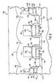
- FIG. 1is a schematic of a chemical vapor deposition system suitable for use in the method of the present invention.
- FIG. 2is a schematic of an alternative chemical vapor deposition system suitable for use in the method of the present invention.
- FIG. 3is a diagrammatic cross-sectional view taken along a portion of a semiconductor wafer at an early processing step according to one embodiment of the present invention.
- FIG. 4is a diagrammatic cross-sectional view of a portion of a semiconductor wafer at a processing step subsequent to that shown in FIG. 3.
- FIG. 5is a diagrammatic cross-sectional view of a portion of a semiconductor wafer at a processing step subsequent to that shown in FIG. 4.
- FIG. 6is a diagrammatic cross-sectional view of a portion of a semiconductor wafer at a processing step subsequent to that shown in FIG. 5.
- FIG. 7is a diagrammatic cross-sectional view of a portion of a semiconductor wafer at a processing step subsequent to that shown in FIG. 6.
- FIG. 8is a diagrammatic cross-sectional view of a portion of a semiconductor wafer at a processing step subsequent to that shown in FIG. 7.
- FIG. 9is a diagrammatic cross-sectional view of a portion of a semiconductor wafer at a processing step subsequent to that shown in FIG. 8.
- FIG. 10is a diagrammatic cross-sectional view of a portion of a semiconductor wafer at a processing step subsequent to that shown in FIG. 9.
- FIG. 11is a diagrammatic cross-sectional view of a portion of a semiconductor wafer at a processing step subsequent to that shown in FIG. 10.
- FIG. 12is a diagrammatic cross-sectional view of a portion of a semiconductor wafer at a processing step subsequent to that shown in FIG. 11.
- FIG. 13is a diagrammatic cross-sectional view of a portion of a semiconductor wafer at a processing step subsequent to that shown in FIG. 12.
- FIG. 14is a diagrammatic cross-sectional view taken along a portion of a semiconductor wafer at a processing step according to another embodiment of the present invention.
- FIG. 15is a diagrammatic cross-sectional view taken along a portion of a semiconductor wafer at processing step according to still another embodiment of the present invention.
- FIG. 16is a diagrammatic cross-sectional view taken along a portion of a semiconductor wafer at processing step according to yet a further embodiment of the present invention.
- FIG. 17is a diagrammatic cross-sectional view of a portion of a semiconductor wafer at a processing step subsequent to that shown in FIG. 16.
- the mixed metal boride, nitride, and boride-nitride barrier materials of the inventiongenerally have the formula M x Al y N z B w , wherein M is Ti, Zr, Hf, V, Nb, Ta, Cr, Mo or W, and x, y, z, and w are any suitable value such that x is greater than zero; y is greater than or equal to zero; the sum of z and w is greater than zero; and wherein when y is zero, z and w are both greater than zero, and when M is Ti, w is greater than 0.
- Mpreferred metals
- Mare Ti, Zr, Hf, Ta, Nb, Mo and W.
- Mis Ti, Zr, Hf, Ta, or Nb
- Mis Mo or W
- Mis Ti, Zr, Hf, Ta, or Nb and M x Al y N z B w has the formula M 0.7 Al 0.3 N 0.3 B 1.4
- Mis Mo, or W
- M x Al y N z B whas the formula M 0.7 Al 0.3 N 0.3 B 0.35 .
- the M x Al y N z B w barrier materialcan be deposited by a sputter process from metal nitride and metal boride targets, or sputtered from metal targets in the presence of boron and nitrogen containing gases, such as diborane, ammonia and nitrogen.
- the barrier materialcan also be deposited by chemical vapor deposition utilizing a volatile source for M and Al and a reactive gas source for N and B.
- metal sources for Al depositioninclude, such as, dimethylaluminumhydride (DMAH) and triethylaluminum (TEAL).
- Sources for Minclude any metal halide or organometallic compound suitable for a CVD process.
- the M x Al y N z B w barrier materialcan also be deposited by liquid spin-on or dip coat processes utilizing a metalorganic solution that is baked and annealed after application. Chemical vapor deposition techniques are preferred, because they generally are more suitable for deposition on semiconductor substrates or substrate assemblies, particularly in contact openings which are extremely small and require conformally filled layers.
- the methods of the present inventioncan be used to deposit a barrier material film on a variety of substrates, such as a semiconductor wafer (e.g., silicon wafer, gallium arsenide wafer, etc.), glass plate, etc., and on a variety of surfaces of the substrates, whether it be directly on the substrate itself or on a layer of material deposited on the substrate as in a semiconductor substrate assembly.
- Metal and other components of the barrier filmmay be deposited from either a volatile liquid, a sublimable solid, or a solid that is soluble in a suitable solvent that is not detrimental to the substrate, and other layers thereon.
- solventsare not used; rather, the metal components are liquid and used neat.
- Methods of the present inventionpreferably utilize vapor deposition techniques, such as flash vaporization, bubbling, etc.
- FIG. 1A typical chemical vapor deposition (CVD) system that can be used to perform the process of the present invention is shown in FIG. 1.
- the systemincludes an enclosed chemical vapor deposition chamber 210 , which may be a cold wall-type CVD reactor.
- the CVD processmay be carried out at pressures of from atmospheric pressure down to about 10 ⁇ 3 torr, and preferably from about 10 torr to about 0.1 torr.
- a vacuummay be created in chamber 210 using turbo pump 212 and backing pump 214 .
- One or more substrates 216are positioned in chamber 210 .
- a constant nominal temperatureis established for the substrate, preferably at a temperature of about 100° C. to about 600° C., and more preferably at a temperature of about 250° C. to about 550° C.
- Substrate 216may be heated, for example, by an electrical resistance heater 218 on which substrate 216 is mounted. Other known methods of heating the substrate may also be utilized.
- the precursor composition 240which contains one or more metal or metalloid complexes, is stored in liquid form (a neat liquid at room temperature or at an elevated temperature if solid at room temperature) in vessel 242 .
- a source 244 of a suitable inert gasis pumped into vessel 242 and bubbled through the neat liquid (i.e., without solvent) picking up the precursor composition and carrying it into chamber 210 through line 245 and gas distributor 246 .
- Additional inert carrier gas or reaction gasmay be supplied from source 248 as needed to provide the desired concentration of precursor composition and regulate the uniformity of the deposition across the surface of substrate 216 .
- a series of valves 250 - 254are opened and closed as required.
- the precursor compositionis pumped into the CVD chamber 210 at a flow rate of about 1 sccm (standard cubic centimeters) to about 1000 sccm.
- the semiconductor substrateis exposed to the precursor composition at a pressure of about 0.001 torr to about 100 torr for a time of about 0.01 minute to about 100 minutes.
- the precursor compositionwill form an adsorbed layer on the surface of the substrate 216 .
- the deposition rateis temperature dependent, increasing the temperature of the substrate will increase the rate of deposition. Typical deposition rates are about 10 Angstroms/minute to about 1000 Angstroms/minute.
- the carrier gas containing the precursor compositionis terminated by dosing valve 253 .
- FIG. 2An alternative CVD system that can be used to perform the mixed metal nitride and boride CVD process of the present invention is shown in FIG. 2.
- the systemincludes an enclosed chemical vapor deposition chamber 210 , which may be a cold wall-type CVD reactor, in which a vacuum may be created using turbo pump 212 and backing pump 214 .
- One or more substrates 216e.g., semiconductor substrates or substrate assemblies
- Substrate 216may be heated as described with reference to FIG. 1 (for example, by an electrical resistance heater 218 ).
- one or more solutions 260 of one or more precursor metal or metalloid complexesare stored in vessels 262 .
- the solutionsare transferred to a mixing manifold 264 using pumps 266 .
- the resultant precursor compositions containing one or more precursor complexes and one or more organic solventsis then transferred along line 268 to vaporizer 270 , to volatilize the precursor composition.
- a source 274 of a suitable inert gasis pumped into vaporizer 270 for carrying a volatilized precursor composition into chamber 210 through line 275 and gas distributor 276 .
- Reaction gasmay be supplied from source 278 as needed.
- a series of valves 280 - 285are opened and closed as required. Similar pressures and temperatures to those described with reference to FIG. 1 can be used.
- carrier gases and/or reaction gasescan be used in certain methods of the present invention. They can be introduced into the chemical vapor deposition chamber in a variety of manners, such as directly into the vaporization chamber or in combination with the precursor composition. Although specific vapor deposition processes are described by reference to FIGS. 1 - 2 , methods of the present invention are not limited to being used with the specific vapor deposition systems shown.
- Various CVD process chambers or reaction chamberscan be used, including hot wall or cold wall reactors, atmospheric or reduced pressure reactors, as well as plasma enhanced reactors.
- the use of the mixed metal nitride and boride materials and methods of forming layers and films of the present inventionare beneficial for a wide variety of applications in semiconductor structures, particularly those using high dielectric materials or ferroelectric materials.
- Such applicationsinclude capacitors such as planar cells, trench cells (e.g., double sidewall trench capacitors), stacked cells (e.g., crown, V-cell, delta cell, multi-fingered, or cylindrical container stacked capacitors), as well as field effect transistor devices, and any semiconductor device having a silicon-metal interface.
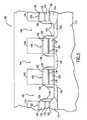
- a typical semiconductor wafer fragment at an early processing stepis indicated generally by reference numeral 100 .
- the semiconductor wafer 100is comprised of a bulk silicon substrate 112 with field isolation oxide regions 114 and active areas 116 , 118 , 120 .
- Word lines 122 , 124 , 126 , 128have been constructed on the wafer 100 in a conventional manner. Each word line consisting of a lower gate oxide 130 , a lower poly layer 132 , a higher conductivity silicide layer 134 and an insulating silicon nitride cap 136 . Each word line has also been provided with insulating spacers 138 , also of silicon nitride.
- Two FETsare depicted in FIG. 3.
- One FETis comprised of two active areas (source/drain) 116 , 118 and one word line (gate) 124 .
- the second FETis comprised of two active areas (source/drain) 118 , 120 and a second word line (gate) 126 .
- the active area 118 common to both FETsis the active area over which a bit line contact will be formed.
- a thin layer 140 of nitride or TEOSis provided atop the wafer 100 .
- a layer of insulating material 142is deposited.
- the insulating materialpreferably consists of borophosphosilicate glass (BPSG).
- BPSGborophosphosilicate glass
- CMPchemical-mechanical polishing
- a bit line contact opening 144 and capacitor openings 146have been formed through the insulating layer 142 .
- the openings 144 , 146are formed through the insulating layer 142 by photomasking and dry chemical etching the BPSG relative to the thin nitride or TEOS layer 140 .
- a layer 150 of conductive materialis deposited to provide conductive material within the bit line contact and capacitor openings 144 , 146 .
- the conductive layer 150is in contact with the active areas 116 , 118 , 120 .
- An example of the material used to form layer 150is in situ arsenic or phosphorous doped poly.
- the conductive layer 150is etched away to the point that the only remaining material forms plugs 150 over the active areas 116 , 118 , 120 .
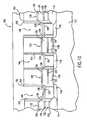
- a thin barrier film 151 of a mixed metal boride, nitride or boride-nitride of the formula M x Al y N z B w as defined aboveis formed as a barrier layer atop conductive layer 150 .
- Barrier film 151is preferably deposited by CVD to form a conformal layer which protects the subsequently deposited capacitor dielectric against diffusion from underlying plug 150 and other surrounding materials. Perhaps more importantly for some applications of the invention, barrier film 151 also protects the underlying plug 150 from diffusion of oxygen from the capacitor dielectric.
- the preferred method for depositing barrier layer 15includes positioning the wafer assembly within a vacuum CVD reactor chamber.
- the CVD reactorwill be a cold wall reactor.
- the substratewill be heated by a resistive-type ceramic heater to a temperature of 250-550° C.
- Hydrogen gaswill inlet to the chamber at a rate of approximately 50-500 sccm.
- the metal (M), aluminum, nitrogen, and boron precursorswill be admitted into the CVD chamber.
- the metal (M)is Ti
- the titanium precursorwill be of the formula Ti(NR 2 ) 4 , where R is selected from the group consisting of H an alkyl and/or aryl group.
- any suitable organometallic or inorganic titanium containing sourcemay be substituted for Ti(NR 2 ) 4 .
- the same gaswill serve as both the titanium and nitrogen precursor.
- the titanium precursorwill be a titanium organometallic precursor, having the formula Ti(N(CH 3 ) 2 ) 4 , which is commonly referred to as TDMAT.
- the aluminum precursorwill preferably be dimethylethylaminealane, commonly known as DMEAA.
- any suitable organometallic or inorganic aluminum containing sourcemay be substituted for DMEAA Both of these reaction precursors are liquids at room temperature, and must be bubbled with helium, or otherwise vaporized, such as through injection into a vaporizer to facilitate transport as gases into the CVD chamber for deposition on the substrate.
- Sources as precursors for Ti, Zr, Hf, V, Nb, Ta, Cr, Mo and Wcan be any suitable metal halide or organometallic compound containing Ti, Zr, Hf, V, Nb, Ta, Cr, Mo or W.
- a bubblerwill be used for each precursor, and each bubbler will be held at the same pressure as that within the CVD chamber.
- a TDMAT bubblerwill preferably be maintained at a temperature of 35-55° C., with helium being flowed through at a rate of approximately 20-200 sccm.
- the DMEAA vesselwill be maintained at a temperature of approximately 5-30° C., with the helium passed through at a rate of 10-100 sccm.
- Other systemsmay be utilized for introducing one or more precursors into the CVD chamber.
- a precursormay be introduced into the CVD chamber by direct liquid injection.
- precursorsmay be introduced in vapor or liquid form, such as in liquid source CVD (LSCVD) operations.
- LSCVDliquid source CVD
- the precursorsare bubbled into the CVD chamber, and are mixed in a gas distributor, such as a gas “showerhead”, and are directed onto the heated substrate.
- a gas distributorsuch as a gas “showerhead”
- Depositionmay be continued for the desired period of time.
- the metal, aluminum, nitrogen, and boronwill thus preferably be deposited generally simultaneously, as an amorphous material.
- the depositionmay continue for approximately 3-10 minutes, after which time the gas flows will be stopped, and the substrate allowed to cool.
- DMEAA precursor gasis described relative to the exemplary embodiment above, an aluminum precursor, aluminum alkyls or alkyl hydride compounds, or their Lewis-based adducts may also be utilized in their place.
- acceptable aluminum precursorscan be, but are not limited to, trimethylaluminum, tris(dimethylamino)aluminum, trimethylaminealane, dimethylalane, or (dimethylethylamine)dimethylalane.
- titanium precursorsare, but are not limited to: the ethyl analog of TDMAT, tetrakisdiethylamidotitanium (also conventionally known as (TDEAT); bis(2,4-dimethyl-1,3-pentadienyl)titanium (also conventionally known as BDPT); titanium tetrachloride; titanium tetrabromide; titanium tetraiodide; and cyclopentadienylcycloheptatrienyltitanium (also conventionally known as CpTiChT).
- exemplary products for other metal precursorsinclude CpZr(BH 4 ) 2 , CpHf(BH 4 ) 2 , TaCl, WF 6 , and MoF 6 ,
- Examples of reactive gas sources for nitrogen and boroninclude, but are not limited to NF 3 , N 2 (especially with plasma assist), NH 3 , hydrazine, methyl hydrazine, B 2 H 6 , and BCl 3 .
- a layer 152 of conductive material that will eventually form one of the electrodes of the capacitoris deposited at a thickness such that the capacitor openings 144 , 146 are not closed off.
- the layer 152may be formed of various refractive metals, conductive metal oxides, metal nitrides, noble metals and may include, such as, Pt, Rh, Ir, Ru, Os, Pd, IrO 2 , RhO 2 , RuO 2 , Ta, TiN, TaN, Ti and others.
- the conductive layer 152is in electrical contact with the previously formed plugs 150 or, as previously mentioned, the M x Al y N z B w layer will itself be the lower electrode.
- the portion of the conductive layer 152 above the top of the BPSG layer 142is removed through a planarized etching process, thereby electrically isolating the portions of layer 152 remaining in the bit line contact and capacitor openings 144 , 146 .
- a capacitor dielectric layer 154is provided over conductive layer 152 and capacitor openings 144 , 146 .
- Dielectric layer 154is deposited with a thickness such that the openings 146 are again not completely filled.
- Dielectric layer 154may comprise tantalum pentoxide (Ta 2 O 5 ).
- Other suitable dielectric materialssuch as Strontium Titanate (ST), Barium Strontium Titanate (BST), Lead Zirconium Titanate (PZT), Strontium Bismuth Tantalate (SBT) and Bismuth Zirconium Titanate (BZT) may also be used.
- Dielectric layer 154may be deposited by a low-pressure CVD process using Ta(OC 2 H 5 ) 5 and O 2 at about 430° C., and may be subsequently annealed in order to reduce leakage current characteristics.
- a second conductive electrode layer 156is then deposited by CVD over the dielectric layer 154 , again at a thickness which less than completely fills the capacitor openings 146 .
- the second conductive layer 156may be comprised of TiN, Pt, or other conventional electrode materials, such as many of those previously described for use as conductive layer 152 .
- the second conductive layer 156also forms the interconnection lines between the second plates of all capacitors.
- the second conductive layer 156 and underlying capacitor dielectric layer 154are patterned and etched such that the remaining portions of each group of the first conductive layer 152 , capacitor dielectric layer 154 , and second conductive layer 156 over the bit line contact and capacitor openings 144 , 146 are electrically isolated from each other. In this manner, each of the active areas 116 , 118 , 120 are also electrically isolated (without the influence of the gate). Furthermore, a portion of the first conductive layer 152 in contact with the plug 150 over the bit line active area 118 is outwardly exposed.
- bit line insulating layer 158is provided over the second conductive layer 156 and into the bit line contact opening 144 .
- the bit line insulating layer 158is preferably comprised of BPSG.
- the BPSGis typically reflowed by conventional techniques, i.e., heating to about 800° C.
- Other insulating layerssuch as PSG, or other compositions of doped SiO 2 may similarly be employed as the insulating layer 158 .
- bit line contact opening 160is patterned through the bit line insulating layer 158 such that the barrier film 151 above plug conductive layer 150 is once again outwardly exposed. Then a bit line contact is provided in the bit line contact opening 160 such that the bit line contact is in electrical contact with the outwardly exposed portion of the barrier film 151 above conductive plug layer 150 .
- the plug 150 over the active area 118 common to both FETsacts as a bit line contact.
- the DRAM array and associated circuitrymay then be completed by a variety of well established techniques, such as metalization, and attachment to peripheral circuitry.
- the memory cell 310includes a ferroelectric material 311 , which is prepared by depositing one or more of the materials discussed herein preferably using chemical vapor techniques, between two electrodes 312 and 313 , which are typically made of platinum, although other metals such as gold or aluminum can also be used.
- the bottom electrode 313is typically in contact with a silicon-containing layer 314 , such as an n-type or p-type silicon substrate, silicon dioxide, glass, etc.
- a conductive mixed metal nitride and boride barrier layer 315is positioned between the bottom electrode 313 and the silicon-containing layer 314 to act as a barrier layer to diffusion of atoms such as silicon into the electrode and ferroelectric material.
- the substrate 416may be in the form of an n channel MOSFET (n-channel metal-oxide semiconductor field-effect transistor), which may be used in a DRAM memory device.
- substrate 416is a p-type silicon having two n-type silicon islands 420 and 422 , representing the transistor source and drain.
- the gate for the transistoris formed by a metal/polysilicon layer 424 deposited over a silicon dioxide layer 426 .
- a relatively thick layer of an insulating silicon dioxide 428overlies the active areas on substrate 416 .
- contacts 430 and 432have been etched through oxide layer 428 down to the surface of substrate 416 .
- a metal or metal silicide layer 434such as titanium silicide, is deposited and formed at the base of contacts 430 and 432 .
- a thin, conformal barrier layer of a mixed metal boride and nitride 436is deposited by CVD over the walls of the contacts. Because of the presence of the conductive barrier layer, the electrical contact path is excellent and the aluminum metal 438 which is deposited over the mixed metal boride and nitride barrier layer 436 is prevented from attacking the substrate surfaces.
- a conductive layer 518may be deposited to fill the cavity formed in layer 514 over the substrate contact region 515 .
- Conductive layer 518may be, for example, aluminum or tungsten.
- layers 516 and 518may removed, such as by being patterned and etched in a desired manner to form interconnects between substrate regions.
- conductive layer 518 and barrier layer 516could be etched away to form a conductive plug structure as shown in FIG. 17.
- the mixed-metal nitride and boride barrier layer and electrode materials according to the inventionhave excellent conductivity, and therefor reduce depletion effects and enhance frequency response.
- the materialspossess excellent barrier properties for protection of cell dielectrics and substrate during oxidation/recrystallization steps for dielectrics and during BPGS reflow and other high temperature steps after capacitor formation.
- the barriers according to the inventionalso substantially prevent diffusion to protect cell dielectrics from interaction with Si and other surrounding materials which may degrade the dielectric materials or produce an additional SiO 2 dielectric layer.
- the barriers/electrodes of the inventionare not limited to use as barrier films for bottom electrodes, but may also be employed both as top and bottom electrodes, and as additional barrier layers applied to any other top and/or bottom electrodes.
- the compositions and methods of forming barrier films of the present inventionare also beneficial for a wide variety of thin film applications in integrated circuit structures, particularly those using high dielectric materials and/or silicon-metal interfaces.
- the method of the preferred embodiments of the inventionprevent degradation of an electrical connection between a conductive layer and a semiconductor substrate by providing a diffusion barrier between the two regions.
Landscapes
- Engineering & Computer Science (AREA)
- Power Engineering (AREA)
- Computer Hardware Design (AREA)
- Condensed Matter Physics & Semiconductors (AREA)
- General Physics & Mathematics (AREA)
- Physics & Mathematics (AREA)
- Microelectronics & Electronic Packaging (AREA)
- Manufacturing & Machinery (AREA)
- Chemical & Material Sciences (AREA)
- Chemical Kinetics & Catalysis (AREA)
- General Chemical & Material Sciences (AREA)
- Semiconductor Memories (AREA)
- Electrodes Of Semiconductors (AREA)
Abstract
Description
- The invention relates generally to integrated circuits and more particularly to the use of amorphous ternary aluminum nitride and boride alloy materials for diffusion barrier layers in such circuits.[0001]
- In semiconductor devices, it is common for the design to require interfaces of silicon and a metal such as aluminum or tungsten. For example, aluminum and tungsten are commonly used as the material of choice for electrical contacts, which contacts interface with electrically active areas made of doped silicon. It is also common in the fabrication of semiconductor devices to anneal the devices at elevated temperatures, such as 500° C. At these temperatures, the metal and silicon will rapidly interdiffuse into each other at the interface. Even at room temperature, the metal and silicon will interdiffuse over time. Such interdiffusion changes the semiconductive properties of the silicon and causes defective devices.[0002]
- Capacitors are used in a wide variety of integrated circuits and present special interdiffusion concerns. Capacitors are of particular concern in DRAM (dynamic random access memory) circuits. The electrodes in a DRAM cell capacitor must protect the dielectric film (e.g., Ta[0003]2O5and (Ba, Sr)TiO3) from interaction with surrounding materials and from the harsh thermal processing encountered in subsequent steps of DRAM process flow. In order to function well as a bottom electrode, the electrode film or film stack must act as an effective barrier to the diffusion of oxygen and silicon. Oxidation of the underlying Si results in decreased series capacitance, thus degrading the capacitor.
- It is common practice to provide diffusion barriers in semiconductor devices. A thin film of titanium nitride (TiN) or titanium tungsten (TiW) is conventionally used as diffusion barrier. Conventional barrier materials, however, tend to be polycrystalline with grain boundaries through which diffusion of Si and O atomic species can occur.[0004]
- The conventional diffusion barriers for silicon/metal interfaces and capacitor dielectrics, while generally relatively effective at room temperature, can fail at more elevated temperatures. Many preferred semiconductor fabrication processes, such as deposition, reflow, and annealing, require elevated temperatures. Thus conventional diffusion barriers can create limits on the processes that can be used to fabricate a semiconductor device. There is a need for a diffusion barrier that is more effective than conventional polycrystalline barriers, especially at elevated temperatures.[0005]
- What is needed are improved diffusion barrier layers and fabrication methods that offer a combination of good conformality, high conductivity, and excellent barrier properties for protecting against interdiffusion at capacitor dielectrics and silicon/metal interfaces in semiconductor devices, particularly during high temperature fabrication processes.[0006]
- The present invention provides mixed-metal nitride, boride and boride-nitride alloy barrier layers of the formula M[0007]xAlyNzBw, wherein M is Ti, Zr, Hf, V, Nb, Ta, Cr, Mo, or W; x is greater than zero; y is greater than or equal to zero; the sum of z and w is greater than zero; and wherein when y is zero, z and w are both greater than zero, and when M is Ti, w is greater than 0.
- The preferred metals (M) are Ti, Zr, Hf, Ta, Nb, Mo and W. Preferably, when M is Ti, Zr, Hf, Ta, or Nb, x+y=1, and z+w/2=1; and when M is Mo or W, x+y=1, and z+2w=1. Most preferably, M is Ti, Zr, Hf, Ta, or Nb and M[0008]xAlyNzBwhas the formula M0.7Al0.3N0.3B1.4, or M is Mo, or W, and MxAlyNzBwhas the formula M0.7Al0.3N0.3B0.35.
- The invention also provides semiconductor capacitors and methods for fabricating capacitors and other devices containing M[0009]xAlyNzBwbarrier layers in order to protect capacitor cell dielectrics, such as SiO2, Ta2O5, SrTiO3(“ST”), (Ba, Sr)TiO3(“BST”), Pb(Z, Ti)O3(“PZT”), SrBi2Ta2O9(“SBT”) and Ba(Zr, Ti)O3(“BZT”).
- The mixed-metal nitride and boride layers of the invention provide excellent barrier protection, conductivity as capacitor electrodes, and conformality, and so may be employed either as capacitor electrodes, or as separate barrier layers formed adjacent to conventional capacitor electrodes, either atop these electrodes or interposed between the electrode and the capacitor dielectric. Preferably, the M[0010]xAlyNzBwlayer according to the invention comprises a thin barrier film between a cell dielectric and an underlying polysilicon (poly) plug or drain in a DRAM cell array, as well as acting as a lower electrode.
- The barrier layers and methods of the invention are also useful in any device containing a Si/metal interface, and any other semiconductor device where protection against degradation through diffusion and thermal effects is desired.[0011]
- FIG. 1 is a schematic of a chemical vapor deposition system suitable for use in the method of the present invention.[0012]
- FIG. 2 is a schematic of an alternative chemical vapor deposition system suitable for use in the method of the present invention.[0013]
- FIG. 3 is a diagrammatic cross-sectional view taken along a portion of a semiconductor wafer at an early processing step according to one embodiment of the present invention.[0014]
- FIG. 4 is a diagrammatic cross-sectional view of a portion of a semiconductor wafer at a processing step subsequent to that shown in FIG. 3.[0015]
- FIG. 5 is a diagrammatic cross-sectional view of a portion of a semiconductor wafer at a processing step subsequent to that shown in FIG. 4.[0016]
- FIG. 6 is a diagrammatic cross-sectional view of a portion of a semiconductor wafer at a processing step subsequent to that shown in FIG. 5.[0017]
- FIG. 7 is a diagrammatic cross-sectional view of a portion of a semiconductor wafer at a processing step subsequent to that shown in FIG. 6.[0018]
- FIG. 8 is a diagrammatic cross-sectional view of a portion of a semiconductor wafer at a processing step subsequent to that shown in FIG. 7.[0019]
- FIG. 9 is a diagrammatic cross-sectional view of a portion of a semiconductor wafer at a processing step subsequent to that shown in FIG. 8.[0020]
- FIG. 10 is a diagrammatic cross-sectional view of a portion of a semiconductor wafer at a processing step subsequent to that shown in FIG. 9.[0021]
- FIG. 11 is a diagrammatic cross-sectional view of a portion of a semiconductor wafer at a processing step subsequent to that shown in FIG. 10.[0022]
- FIG. 12 is a diagrammatic cross-sectional view of a portion of a semiconductor wafer at a processing step subsequent to that shown in FIG. 11.[0023]
- FIG. 13 is a diagrammatic cross-sectional view of a portion of a semiconductor wafer at a processing step subsequent to that shown in FIG. 12.[0024]
- FIG. 14 is a diagrammatic cross-sectional view taken along a portion of a semiconductor wafer at a processing step according to another embodiment of the present invention.[0025]
- FIG. 15 is a diagrammatic cross-sectional view taken along a portion of a semiconductor wafer at processing step according to still another embodiment of the present invention.[0026]
- FIG. 16 is a diagrammatic cross-sectional view taken along a portion of a semiconductor wafer at processing step according to yet a further embodiment of the present invention.[0027]
- FIG. 17 is a diagrammatic cross-sectional view of a portion of a semiconductor wafer at a processing step subsequent to that shown in FIG. 16.[0028]
- The mixed metal boride, nitride, and boride-nitride barrier materials of the invention generally have the formula M[0029]xAlyNzBw, wherein M is Ti, Zr, Hf, V, Nb, Ta, Cr, Mo or W, and x, y, z, and w are any suitable value such that x is greater than zero; y is greater than or equal to zero; the sum of z and w is greater than zero; and wherein when y is zero, z and w are both greater than zero, and when M is Ti, w is greater than 0. The preferred metals (“M”) are Ti, Zr, Hf, Ta, Nb, Mo and W. Preferably, when M is Ti, Zr, Hf, Ta, or Nb, x+y=1, and z+w/2=1, and when M is Mo or W, x+y=1, and z+2w=1. Most preferably, M is Ti, Zr, Hf, Ta, or Nb and MxAlyNzBwhas the formula M0.7Al0.3N0.3B1.4, or M is Mo, or W, and MxAlyNzBwhas the formula M0.7Al0.3N0.3B0.35.
- The M[0030]xAlyNzBwbarrier material can be deposited by a sputter process from metal nitride and metal boride targets, or sputtered from metal targets in the presence of boron and nitrogen containing gases, such as diborane, ammonia and nitrogen. The barrier material can also be deposited by chemical vapor deposition utilizing a volatile source for M and Al and a reactive gas source for N and B. Examples of metal sources for Al deposition include, such as, dimethylaluminumhydride (DMAH) and triethylaluminum (TEAL). Sources for M include any metal halide or organometallic compound suitable for a CVD process. The MxAlyNzBwbarrier material can also be deposited by liquid spin-on or dip coat processes utilizing a metalorganic solution that is baked and annealed after application. Chemical vapor deposition techniques are preferred, because they generally are more suitable for deposition on semiconductor substrates or substrate assemblies, particularly in contact openings which are extremely small and require conformally filled layers.
- The methods of the present invention can be used to deposit a barrier material film on a variety of substrates, such as a semiconductor wafer (e.g., silicon wafer, gallium arsenide wafer, etc.), glass plate, etc., and on a variety of surfaces of the substrates, whether it be directly on the substrate itself or on a layer of material deposited on the substrate as in a semiconductor substrate assembly. Metal and other components of the barrier film may be deposited from either a volatile liquid, a sublimable solid, or a solid that is soluble in a suitable solvent that is not detrimental to the substrate, and other layers thereon. Preferably, however, solvents are not used; rather, the metal components are liquid and used neat. Methods of the present invention preferably utilize vapor deposition techniques, such as flash vaporization, bubbling, etc.[0031]
- A typical chemical vapor deposition (CVD) system that can be used to perform the process of the present invention is shown in FIG. 1. The system includes an enclosed chemical[0032]
vapor deposition chamber 210, which may be a cold wall-type CVD reactor. As is conventional, the CVD process may be carried out at pressures of from atmospheric pressure down to about 10−3torr, and preferably from about 10 torr to about 0.1 torr. A vacuum may be created inchamber 210 usingturbo pump 212 andbacking pump 214. - One or more substrates[0033]216 (e.g., semiconductor substrates or substrate assemblies) are positioned in
chamber 210. A constant nominal temperature is established for the substrate, preferably at a temperature of about 100° C. to about 600° C., and more preferably at a temperature of about 250° C. to about 550°C. Substrate 216 may be heated, for example, by anelectrical resistance heater 218 on whichsubstrate 216 is mounted. Other known methods of heating the substrate may also be utilized. - In this process, the[0034]
precursor composition 240, which contains one or more metal or metalloid complexes, is stored in liquid form (a neat liquid at room temperature or at an elevated temperature if solid at room temperature) invessel 242. Asource 244 of a suitable inert gas is pumped intovessel 242 and bubbled through the neat liquid (i.e., without solvent) picking up the precursor composition and carrying it intochamber 210 throughline 245 andgas distributor 246. Additional inert carrier gas or reaction gas may be supplied fromsource 248 as needed to provide the desired concentration of precursor composition and regulate the uniformity of the deposition across the surface ofsubstrate 216. As shown, a series of valves250-254 are opened and closed as required. - Generally, the precursor composition is pumped into the[0035]
CVD chamber 210 at a flow rate of about 1 sccm (standard cubic centimeters) to about 1000 sccm. The semiconductor substrate is exposed to the precursor composition at a pressure of about 0.001 torr to about 100 torr for a time of about 0.01 minute to about 100 minutes. Inchamber 210, the precursor composition will form an adsorbed layer on the surface of thesubstrate 216. As the deposition rate is temperature dependent, increasing the temperature of the substrate will increase the rate of deposition. Typical deposition rates are about 10 Angstroms/minute to about 1000 Angstroms/minute. The carrier gas containing the precursor composition is terminated bydosing valve 253. - An alternative CVD system that can be used to perform the mixed metal nitride and boride CVD process of the present invention is shown in FIG. 2. The system includes an enclosed chemical[0036]
vapor deposition chamber 210, which may be a cold wall-type CVD reactor, in which a vacuum may be created usingturbo pump 212 andbacking pump 214. One or more substrates216 (e.g., semiconductor substrates or substrate assemblies) are positioned inchamber 210.Substrate 216 may be heated as described with reference to FIG. 1 (for example, by an electrical resistance heater218). - In this process, one or[0037]
more solutions 260 of one or more precursor metal or metalloid complexes are stored invessels 262. The solutions are transferred to a mixingmanifold 264 usingpumps 266. The resultant precursor compositions containing one or more precursor complexes and one or more organic solvents is then transferred alongline 268 tovaporizer 270, to volatilize the precursor composition. Asource 274 of a suitable inert gas is pumped intovaporizer 270 for carrying a volatilized precursor composition intochamber 210 throughline 275 and gas distributor276. Reaction gas may be supplied fromsource 278 as needed. As shown, a series of valves280-285 are opened and closed as required. Similar pressures and temperatures to those described with reference to FIG. 1 can be used. - Various combinations of carrier gases and/or reaction gases can be used in certain methods of the present invention. They can be introduced into the chemical vapor deposition chamber in a variety of manners, such as directly into the vaporization chamber or in combination with the precursor composition. Although specific vapor deposition processes are described by reference to FIGS.[0038]1-2, methods of the present invention are not limited to being used with the specific vapor deposition systems shown. Various CVD process chambers or reaction chambers can be used, including hot wall or cold wall reactors, atmospheric or reduced pressure reactors, as well as plasma enhanced reactors.
- The use of the mixed metal nitride and boride materials and methods of forming layers and films of the present invention are beneficial for a wide variety of applications in semiconductor structures, particularly those using high dielectric materials or ferroelectric materials. Such applications include capacitors such as planar cells, trench cells (e.g., double sidewall trench capacitors), stacked cells (e.g., crown, V-cell, delta cell, multi-fingered, or cylindrical container stacked capacitors), as well as field effect transistor devices, and any semiconductor device having a silicon-metal interface.[0039]
- Examples of fabrication processes for capacitors and other semiconductor devices containing mixed metal nitride, boride and nitride-boride barrier layers of the formula M[0040]xAlyNzBware described below. It is to be understood, however, that these processes are only examples of many possible configurations and processes utilizing the barriers or electrodes of the invention. For example, in the DRAM cell stacked container capacitor process described next, a mixed metal nitride and boride material is utilized as a barrier below the bottom electrode of a capacitor. Alternatively, the top electrode may also include a barrier material. The invention is not intended to be limited by the particular processes described below.
- Referring to FIG. 3, a typical semiconductor wafer fragment at an early processing step is indicated generally by[0041]
reference numeral 100. Thesemiconductor wafer 100 is comprised of abulk silicon substrate 112 with fieldisolation oxide regions 114 andactive areas Word lines wafer 100 in a conventional manner. Each word line consisting of alower gate oxide 130, alower poly layer 132, a higherconductivity silicide layer 134 and an insulatingsilicon nitride cap 136. Each word line has also been provided with insulatingspacers 138, also of silicon nitride. - Two FETs are depicted in FIG. 3. One FET is comprised of two active areas (source/drain)[0042]116,118 and one word line (gate)124. The second FET is comprised of two active areas (source/drain)118,120 and a second word line (gate)126. The
active area 118 common to both FETs is the active area over which a bit line contact will be formed. - Referring to FIG. 4, a[0043]
thin layer 140 of nitride or TEOS is provided atop thewafer 100. Next a layer of insulatingmaterial 142 is deposited. The insulating material preferably consists of borophosphosilicate glass (BPSG). The insulatinglayer 142 is subsequently planarized by chemical-mechanical polishing (CMP). - Referring to FIG. 5, a bit[0044]
line contact opening 144 andcapacitor openings 146 have been formed through the insulatinglayer 142. Theopenings layer 142 by photomasking and dry chemical etching the BPSG relative to the thin nitride orTEOS layer 140. Referring now to FIG. 6, alayer 150 of conductive material is deposited to provide conductive material within the bit line contact andcapacitor openings conductive layer 150 is in contact with theactive areas layer 150 is in situ arsenic or phosphorous doped poly. Referring now to FIG. 7, theconductive layer 150 is etched away to the point that the only remaining material forms plugs150 over theactive areas - Referring now to FIG. 8, a[0045]
thin barrier film 151 of a mixed metal boride, nitride or boride-nitride of the formula MxAlyNzBwas defined above is formed as a barrier layer atopconductive layer 150.Barrier film 151 is preferably deposited by CVD to form a conformal layer which protects the subsequently deposited capacitor dielectric against diffusion fromunderlying plug 150 and other surrounding materials. Perhaps more importantly for some applications of the invention,barrier film 151 also protects theunderlying plug 150 from diffusion of oxygen from the capacitor dielectric. - The preferred method for depositing barrier layer[0046]15, includes positioning the wafer assembly within a vacuum CVD reactor chamber. In one preferred implementation, the CVD reactor will be a cold wall reactor. Preferably, the substrate will be heated by a resistive-type ceramic heater to a temperature of 250-550° C. Hydrogen gas will inlet to the chamber at a rate of approximately 50-500 sccm. Subsequently, the metal (M), aluminum, nitrogen, and boron precursors will be admitted into the CVD chamber. Preferably, if the metal (M) is Ti, the titanium precursor will be of the formula Ti(NR2)4, where R is selected from the group consisting of H an alkyl and/or aryl group. However, any suitable organometallic or inorganic titanium containing source may be substituted for Ti(NR2)4. In such case, the same gas will serve as both the titanium and nitrogen precursor. Most preferably, the titanium precursor will be a titanium organometallic precursor, having the formula Ti(N(CH3)2)4, which is commonly referred to as TDMAT. The aluminum precursor will preferably be dimethylethylaminealane, commonly known as DMEAA. However, any suitable organometallic or inorganic aluminum containing source may be substituted for DMEAA Both of these reaction precursors are liquids at room temperature, and must be bubbled with helium, or otherwise vaporized, such as through injection into a vaporizer to facilitate transport as gases into the CVD chamber for deposition on the substrate. Sources as precursors for Ti, Zr, Hf, V, Nb, Ta, Cr, Mo and W, can be any suitable metal halide or organometallic compound containing Ti, Zr, Hf, V, Nb, Ta, Cr, Mo or W.
- In a particularly preferred CVD process according to the present invention, a bubbler will be used for each precursor, and each bubbler will be held at the same pressure as that within the CVD chamber. A TDMAT bubbler will preferably be maintained at a temperature of 35-55° C., with helium being flowed through at a rate of approximately 20-200 sccm. Simultaneously, the DMEAA vessel will be maintained at a temperature of approximately 5-30° C., with the helium passed through at a rate of 10-100 sccm. Other systems may be utilized for introducing one or more precursors into the CVD chamber. For example, in addition to the use of a vaporizer or evaporator, a precursor may be introduced into the CVD chamber by direct liquid injection. Additionally, although the use of gaseous precursors is currently preferred, precursors may be introduced in vapor or liquid form, such as in liquid source CVD (LSCVD) operations.[0047]
- When deposition is to occur, the precursors are bubbled into the CVD chamber, and are mixed in a gas distributor, such as a gas “showerhead”, and are directed onto the heated substrate. Deposition may be continued for the desired period of time. The metal, aluminum, nitrogen, and boron will thus preferably be deposited generally simultaneously, as an amorphous material. In one exemplary implementation, where the M[0048]xAlyNzBwwill be deposited upon a wafer, the deposition may continue for approximately 3-10 minutes, after which time the gas flows will be stopped, and the substrate allowed to cool.
- Although the DMEAA precursor gas is described relative to the exemplary embodiment above, an aluminum precursor, aluminum alkyls or alkyl hydride compounds, or their Lewis-based adducts may also be utilized in their place. Other examples of acceptable aluminum precursors can be, but are not limited to, trimethylaluminum, tris(dimethylamino)aluminum, trimethylaminealane, dimethylalane, or (dimethylethylamine)dimethylalane.[0049]
- Other examples of the exemplary products for titanium precursors are, but are not limited to: the ethyl analog of TDMAT, tetrakisdiethylamidotitanium (also conventionally known as (TDEAT); bis(2,4-dimethyl-1,3-pentadienyl)titanium (also conventionally known as BDPT); titanium tetrachloride; titanium tetrabromide; titanium tetraiodide; and cyclopentadienylcycloheptatrienyltitanium (also conventionally known as CpTiChT). Examples of exemplary products for other metal precursors include CpZr(BH[0050]4)2, CpHf(BH4)2, TaCl, WF6, and MoF6,
- Examples of reactive gas sources for nitrogen and boron include, but are not limited to NF[0051]3, N2(especially with plasma assist), NH3, hydrazine, methyl hydrazine, B2H6, and BCl3.
- Following chemical vapor deposition of a mixed metal nitride and[0052]
boride barrier film 151, alayer 152 of conductive material that will eventually form one of the electrodes of the capacitor is deposited at a thickness such that thecapacitor openings layer 152 may be formed of various refractive metals, conductive metal oxides, metal nitrides, noble metals and may include, such as, Pt, Rh, Ir, Ru, Os, Pd, IrO2, RhO2, RuO2, Ta, TiN, TaN, Ti and others. Theconductive layer 152 is in electrical contact with the previously formedplugs 150 or, as previously mentioned, the MxAlyNzBwlayer will itself be the lower electrode. - Referring to FIG. 10, the portion of the[0053]
conductive layer 152 above the top of theBPSG layer 142 is removed through a planarized etching process, thereby electrically isolating the portions oflayer 152 remaining in the bit line contact andcapacitor openings capacitor dielectric layer 154 is provided overconductive layer 152 andcapacitor openings - [0054]
Dielectric layer 154 is deposited with a thickness such that theopenings 146 are again not completely filled.Dielectric layer 154 may comprise tantalum pentoxide (Ta2O5). Other suitable dielectric materials such as Strontium Titanate (ST), Barium Strontium Titanate (BST), Lead Zirconium Titanate (PZT), Strontium Bismuth Tantalate (SBT) and Bismuth Zirconium Titanate (BZT) may also be used.Dielectric layer 154 may be deposited by a low-pressure CVD process using Ta(OC2H5)5and O2at about 430° C., and may be subsequently annealed in order to reduce leakage current characteristics. - A second[0055]
conductive electrode layer 156 is then deposited by CVD over thedielectric layer 154, again at a thickness which less than completely fills thecapacitor openings 146. The secondconductive layer 156 may be comprised of TiN, Pt, or other conventional electrode materials, such as many of those previously described for use asconductive layer 152. In addition to serving as the top electrode or second plate of the capacitor, the secondconductive layer 156 also forms the interconnection lines between the second plates of all capacitors. - Referring to FIG. 12, the second[0056]
conductive layer 156 and underlyingcapacitor dielectric layer 154 are patterned and etched such that the remaining portions of each group of the firstconductive layer 152,capacitor dielectric layer 154, and secondconductive layer 156 over the bit line contact andcapacitor openings active areas conductive layer 152 in contact with theplug 150 over the bit lineactive area 118 is outwardly exposed. - Referring now to FIG. 12, a bit[0057]
line insulating layer 158 is provided over the secondconductive layer 156 and into the bitline contact opening 144. The bit line insulatinglayer 158 is preferably comprised of BPSG. The BPSG is typically reflowed by conventional techniques, i.e., heating to about 800° C. Other insulating layers such as PSG, or other compositions of doped SiO2may similarly be employed as the insulatinglayer 158. - Referring to FIG. 13, a bit[0058]
line contact opening 160 is patterned through the bitline insulating layer 158 such that thebarrier film 151 above plugconductive layer 150 is once again outwardly exposed. Then a bit line contact is provided in the bitline contact opening 160 such that the bit line contact is in electrical contact with the outwardly exposed portion of thebarrier film 151 aboveconductive plug layer 150. Thus, theplug 150 over theactive area 118 common to both FETs acts as a bit line contact. The DRAM array and associated circuitry may then be completed by a variety of well established techniques, such as metalization, and attachment to peripheral circuitry. - Another specific example of where a film formed from the M[0059]xAlyNxBwmaterials of the present invention is useful is the
ferroelectric memory cell 310 of FIG. 14. Thememory cell 310 includes aferroelectric material 311, which is prepared by depositing one or more of the materials discussed herein preferably using chemical vapor techniques, between twoelectrodes bottom electrode 313 is typically in contact with a silicon-containinglayer 314, such as an n-type or p-type silicon substrate, silicon dioxide, glass, etc. A conductive mixed metal nitride andboride barrier layer 315, preferably deposited by CVD, is positioned between thebottom electrode 313 and the silicon-containinglayer 314 to act as a barrier layer to diffusion of atoms such as silicon into the electrode and ferroelectric material. - Yet another specific example of where a film formed from the material of the present invention is useful is the structure shown in FIG. 15. The[0060]
substrate 416 may be in the form of an n channel MOSFET (n-channel metal-oxide semiconductor field-effect transistor), which may be used in a DRAM memory device. As shown,substrate 416 is a p-type silicon having two n-type silicon islands420 and422, representing the transistor source and drain. Such a construction is well known. The gate for the transistor is formed by a metal/polysilicon layer 424 deposited over asilicon dioxide layer 426. A relatively thick layer of an insulatingsilicon dioxide 428 overlies the active areas onsubstrate 416. - To connect the MOSFET of FIG. 15 with conductive paths on the surface of the device,[0061]
contacts oxide layer 428 down to the surface ofsubstrate 416. A metal or metal silicide layer434, such as titanium silicide, is deposited and formed at the base ofcontacts nitride 436 is deposited by CVD over the walls of the contacts. Because of the presence of the conductive barrier layer, the electrical contact path is excellent and thealuminum metal 438 which is deposited over the mixed metal boride andnitride barrier layer 436 is prevented from attacking the substrate surfaces. - In still another example, as depicted in FIG. 16, after deposition of the M[0062]xAlyNzBwbarrier layer516 within the opening within
layer 514, aconductive layer 518 may be deposited to fill the cavity formed inlayer 514 over thesubstrate contact region 515.Conductive layer 518 may be, for example, aluminum or tungsten. Subsequently, layers516 and518 may removed, such as by being patterned and etched in a desired manner to form interconnects between substrate regions. Alternatively,conductive layer 518 andbarrier layer 516 could be etched away to form a conductive plug structure as shown in FIG. 17. - The mixed-metal nitride and boride barrier layer and electrode materials according to the invention have excellent conductivity, and therefor reduce depletion effects and enhance frequency response. The materials possess excellent barrier properties for protection of cell dielectrics and substrate during oxidation/recrystallization steps for dielectrics and during BPGS reflow and other high temperature steps after capacitor formation. In addition, the barriers according to the invention also substantially prevent diffusion to protect cell dielectrics from interaction with Si and other surrounding materials which may degrade the dielectric materials or produce an additional SiO[0063]2dielectric layer. Thus, the barriers/electrodes of the invention are not limited to use as barrier films for bottom electrodes, but may also be employed both as top and bottom electrodes, and as additional barrier layers applied to any other top and/or bottom electrodes. The compositions and methods of forming barrier films of the present invention are also beneficial for a wide variety of thin film applications in integrated circuit structures, particularly those using high dielectric materials and/or silicon-metal interfaces. The method of the preferred embodiments of the invention prevent degradation of an electrical connection between a conductive layer and a semiconductor substrate by providing a diffusion barrier between the two regions.
- Accordingly, the above description and accompanying drawings are only illustrative of preferred embodiments which can achieve and provide the objects, features and advantages of the present invention. It is not intended that the invention be limited to the embodiments shown and described in detail herein. The invention is only limited by the spirit and scope of the following claims.[0064]
Claims (91)
Priority Applications (2)
| Application Number | Priority Date | Filing Date | Title |
|---|---|---|---|
| US10/642,607US7101779B2 (en) | 1999-03-16 | 2003-08-19 | Method of forming barrier layers |
| US11/509,066US20070045856A1 (en) | 1999-03-16 | 2006-08-24 | Mixed metal nitride and boride barrier layers |
Applications Claiming Priority (3)
| Application Number | Priority Date | Filing Date | Title |
|---|---|---|---|
| US09/268,326US6445023B1 (en) | 1999-03-16 | 1999-03-16 | Mixed metal nitride and boride barrier layers |
| US10/185,009US6664159B2 (en) | 1999-03-16 | 2002-07-01 | Mixed metal nitride and boride barrier layers |
| US10/642,607US7101779B2 (en) | 1999-03-16 | 2003-08-19 | Method of forming barrier layers |
Related Parent Applications (1)
| Application Number | Title | Priority Date | Filing Date |
|---|---|---|---|
| US10/185,009DivisionUS6664159B2 (en) | 1999-03-16 | 2002-07-01 | Mixed metal nitride and boride barrier layers |
Related Child Applications (1)
| Application Number | Title | Priority Date | Filing Date |
|---|---|---|---|
| US11/509,066ContinuationUS20070045856A1 (en) | 1999-03-16 | 2006-08-24 | Mixed metal nitride and boride barrier layers |
Publications (2)
| Publication Number | Publication Date |
|---|---|
| US20040053495A1true US20040053495A1 (en) | 2004-03-18 |
| US7101779B2 US7101779B2 (en) | 2006-09-05 |
Family
ID=23022472
Family Applications (4)
| Application Number | Title | Priority Date | Filing Date |
|---|---|---|---|
| US09/268,326Expired - LifetimeUS6445023B1 (en) | 1999-03-16 | 1999-03-16 | Mixed metal nitride and boride barrier layers |
| US10/185,009Expired - LifetimeUS6664159B2 (en) | 1999-03-16 | 2002-07-01 | Mixed metal nitride and boride barrier layers |
| US10/642,607Expired - Fee RelatedUS7101779B2 (en) | 1999-03-16 | 2003-08-19 | Method of forming barrier layers |
| US11/509,066AbandonedUS20070045856A1 (en) | 1999-03-16 | 2006-08-24 | Mixed metal nitride and boride barrier layers |
Family Applications Before (2)
| Application Number | Title | Priority Date | Filing Date |
|---|---|---|---|
| US09/268,326Expired - LifetimeUS6445023B1 (en) | 1999-03-16 | 1999-03-16 | Mixed metal nitride and boride barrier layers |
| US10/185,009Expired - LifetimeUS6664159B2 (en) | 1999-03-16 | 2002-07-01 | Mixed metal nitride and boride barrier layers |
Family Applications After (1)
| Application Number | Title | Priority Date | Filing Date |
|---|---|---|---|
| US11/509,066AbandonedUS20070045856A1 (en) | 1999-03-16 | 2006-08-24 | Mixed metal nitride and boride barrier layers |
Country Status (1)
| Country | Link |
|---|---|
| US (4) | US6445023B1 (en) |
Cited By (1)
| Publication number | Priority date | Publication date | Assignee | Title |
|---|---|---|---|---|
| US20140231930A1 (en)* | 2013-02-19 | 2014-08-21 | Timothy W. Weidman | Atomic Layer Deposition of Hafnium or Zirconium Alloy Films |
Families Citing this family (89)
| Publication number | Priority date | Publication date | Assignee | Title |
|---|---|---|---|---|
| US6281142B1 (en)* | 1999-06-04 | 2001-08-28 | Micron Technology, Inc. | Dielectric cure for reducing oxygen vacancies |
| US7554829B2 (en) | 1999-07-30 | 2009-06-30 | Micron Technology, Inc. | Transmission lines for CMOS integrated circuits |
| DE10022655C2 (en)* | 2000-04-28 | 2002-03-07 | Infineon Technologies Ag | Process for the production of capacitor structures |
| US6756088B2 (en)* | 2000-08-29 | 2004-06-29 | Micron Technology, Inc. | Methods of forming coatings on gas-dispersion fixtures in chemical-vapor-deposition systems |
| US6787833B1 (en)* | 2000-08-31 | 2004-09-07 | Micron Technology, Inc. | Integrated circuit having a barrier structure |
| US6524912B1 (en) | 2000-08-31 | 2003-02-25 | Micron Technology, Inc. | Planarization of metal container structures |
| DE10058782B4 (en)* | 2000-11-27 | 2006-03-23 | Infineon Technologies Ag | Method for producing a capacitor arrangement |
| US6852167B2 (en) | 2001-03-01 | 2005-02-08 | Micron Technology, Inc. | Methods, systems, and apparatus for uniform chemical-vapor depositions |
| KR100531419B1 (en)* | 2001-06-12 | 2005-11-28 | 주식회사 하이닉스반도체 | semiconductor device and method for fabricating the same |
| JP3886424B2 (en)* | 2001-08-28 | 2007-02-28 | 鹿児島日本電気株式会社 | Substrate processing apparatus and method |
| US8026161B2 (en) | 2001-08-30 | 2011-09-27 | Micron Technology, Inc. | Highly reliable amorphous high-K gate oxide ZrO2 |
| US6844203B2 (en) | 2001-08-30 | 2005-01-18 | Micron Technology, Inc. | Gate oxides, and methods of forming |
| US6717193B2 (en)* | 2001-10-09 | 2004-04-06 | Koninklijke Philips Electronics N.V. | Metal-insulator-metal (MIM) capacitor structure and methods of fabricating same |
| KR100422597B1 (en)* | 2001-11-27 | 2004-03-16 | 주식회사 하이닉스반도체 | Method of forming semiconductor device with capacitor and metal-interconnection in damascene process |
| US6953730B2 (en) | 2001-12-20 | 2005-10-11 | Micron Technology, Inc. | Low-temperature grown high quality ultra-thin CoTiO3 gate dielectrics |
| US6767795B2 (en) | 2002-01-17 | 2004-07-27 | Micron Technology, Inc. | Highly reliable amorphous high-k gate dielectric ZrOXNY |
| US6812100B2 (en) | 2002-03-13 | 2004-11-02 | Micron Technology, Inc. | Evaporation of Y-Si-O films for medium-k dielectrics |
| US7045430B2 (en) | 2002-05-02 | 2006-05-16 | Micron Technology Inc. | Atomic layer-deposited LaAlO3 films for gate dielectrics |
| US7589029B2 (en) | 2002-05-02 | 2009-09-15 | Micron Technology, Inc. | Atomic layer deposition and conversion |
| US7160577B2 (en) | 2002-05-02 | 2007-01-09 | Micron Technology, Inc. | Methods for atomic-layer deposition of aluminum oxides in integrated circuits |
| US7135421B2 (en) | 2002-06-05 | 2006-11-14 | Micron Technology, Inc. | Atomic layer-deposited hafnium aluminum oxide |
| US7205218B2 (en) | 2002-06-05 | 2007-04-17 | Micron Technology, Inc. | Method including forming gate dielectrics having multiple lanthanide oxide layers |
| US6804136B2 (en)* | 2002-06-21 | 2004-10-12 | Micron Technology, Inc. | Write once read only memory employing charge trapping in insulators |
| US7154140B2 (en) | 2002-06-21 | 2006-12-26 | Micron Technology, Inc. | Write once read only memory with large work function floating gates |
| US6970370B2 (en)* | 2002-06-21 | 2005-11-29 | Micron Technology, Inc. | Ferroelectric write once read only memory for archival storage |
| US7193893B2 (en) | 2002-06-21 | 2007-03-20 | Micron Technology, Inc. | Write once read only memory employing floating gates |
| US7221017B2 (en) | 2002-07-08 | 2007-05-22 | Micron Technology, Inc. | Memory utilizing oxide-conductor nanolaminates |
| US7221586B2 (en) | 2002-07-08 | 2007-05-22 | Micron Technology, Inc. | Memory utilizing oxide nanolaminates |
| US6921702B2 (en) | 2002-07-30 | 2005-07-26 | Micron Technology Inc. | Atomic layer deposited nanolaminates of HfO2/ZrO2 films as gate dielectrics |
| US6884739B2 (en) | 2002-08-15 | 2005-04-26 | Micron Technology Inc. | Lanthanide doped TiOx dielectric films by plasma oxidation |
| US6790791B2 (en) | 2002-08-15 | 2004-09-14 | Micron Technology, Inc. | Lanthanide doped TiOx dielectric films |
| US20040036129A1 (en)* | 2002-08-22 | 2004-02-26 | Micron Technology, Inc. | Atomic layer deposition of CMOS gates with variable work functions |
| US6967154B2 (en) | 2002-08-26 | 2005-11-22 | Micron Technology, Inc. | Enhanced atomic layer deposition |
| US7199023B2 (en) | 2002-08-28 | 2007-04-03 | Micron Technology, Inc. | Atomic layer deposited HfSiON dielectric films wherein each precursor is independendently pulsed |
| US7101813B2 (en) | 2002-12-04 | 2006-09-05 | Micron Technology Inc. | Atomic layer deposited Zr-Sn-Ti-O films |
| US6958302B2 (en) | 2002-12-04 | 2005-10-25 | Micron Technology, Inc. | Atomic layer deposited Zr-Sn-Ti-O films using TiI4 |
| JP4031704B2 (en)* | 2002-12-18 | 2008-01-09 | 東京エレクトロン株式会社 | Deposition method |
| JP4290421B2 (en)* | 2002-12-27 | 2009-07-08 | Necエレクトロニクス株式会社 | Semiconductor device and manufacturing method thereof |
| US6863725B2 (en)* | 2003-02-04 | 2005-03-08 | Micron Technology, Inc. | Method of forming a Ta2O5 comprising layer |
| US7192892B2 (en) | 2003-03-04 | 2007-03-20 | Micron Technology, Inc. | Atomic layer deposited dielectric layers |
| US7135369B2 (en) | 2003-03-31 | 2006-11-14 | Micron Technology, Inc. | Atomic layer deposited ZrAlxOy dielectric layers including Zr4AlO9 |
| US7105403B2 (en)* | 2003-07-28 | 2006-09-12 | Micron Technology, Inc. | Double sided container capacitor for a semiconductor device and method for forming same |
| US7230292B2 (en)* | 2003-08-05 | 2007-06-12 | Micron Technology, Inc. | Stud electrode and process for making same |
| US7208427B2 (en)* | 2003-08-18 | 2007-04-24 | Advanced Technology Materials, Inc. | Precursor compositions and processes for MOCVD of barrier materials in semiconductor manufacturing |
| US20050233477A1 (en)* | 2004-03-05 | 2005-10-20 | Tokyo Electron Limited | Substrate processing apparatus, substrate processing method, and program for implementing the method |
| US7482037B2 (en)* | 2004-08-20 | 2009-01-27 | Micron Technology, Inc. | Methods for forming niobium and/or vanadium containing layers using atomic layer deposition |
| JP2006120832A (en)* | 2004-10-21 | 2006-05-11 | Elpida Memory Inc | Semiconductor device and manufacturing method thereof |
| US7374964B2 (en) | 2005-02-10 | 2008-05-20 | Micron Technology, Inc. | Atomic layer deposition of CeO2/Al2O3 films as gate dielectrics |
| US7687409B2 (en) | 2005-03-29 | 2010-03-30 | Micron Technology, Inc. | Atomic layer deposited titanium silicon oxide films |
| US20060223267A1 (en)* | 2005-03-31 | 2006-10-05 | Stefan Machill | Method of production of charge-trapping memory devices |
| US7662729B2 (en) | 2005-04-28 | 2010-02-16 | Micron Technology, Inc. | Atomic layer deposition of a ruthenium layer to a lanthanide oxide dielectric layer |
| US7572695B2 (en) | 2005-05-27 | 2009-08-11 | Micron Technology, Inc. | Hafnium titanium oxide films |
| US7510983B2 (en) | 2005-06-14 | 2009-03-31 | Micron Technology, Inc. | Iridium/zirconium oxide structure |
| US7473637B2 (en)* | 2005-07-20 | 2009-01-06 | Micron Technology, Inc. | ALD formed titanium nitride films |
| US7927948B2 (en) | 2005-07-20 | 2011-04-19 | Micron Technology, Inc. | Devices with nanocrystals and methods of formation |
| US7410910B2 (en) | 2005-08-31 | 2008-08-12 | Micron Technology, Inc. | Lanthanum aluminum oxynitride dielectric films |
| US7615438B2 (en)* | 2005-12-08 | 2009-11-10 | Micron Technology, Inc. | Lanthanide yttrium aluminum oxide dielectric films |
| US7592251B2 (en)* | 2005-12-08 | 2009-09-22 | Micron Technology, Inc. | Hafnium tantalum titanium oxide films |
| US7531416B2 (en)* | 2005-12-21 | 2009-05-12 | E. I. Du Pont De Nemours And Company | Thick film capacitors on ceramic interconnect substrates |
| US7709402B2 (en) | 2006-02-16 | 2010-05-04 | Micron Technology, Inc. | Conductive layers for hafnium silicon oxynitride films |
| EP2029790A1 (en) | 2006-06-02 | 2009-03-04 | L'AIR LIQUIDE, Société Anonyme pour l'Etude et l'Exploitation des Procédés Georges Claude | Method of forming high-k dielectric films based on novel titanium, zirconium, and hafnium precursors and their use for semiconductor manufacturing |
| US7563730B2 (en) | 2006-08-31 | 2009-07-21 | Micron Technology, Inc. | Hafnium lanthanide oxynitride films |
| US7759747B2 (en) | 2006-08-31 | 2010-07-20 | Micron Technology, Inc. | Tantalum aluminum oxynitride high-κ dielectric |
| JP5109394B2 (en)* | 2007-02-14 | 2012-12-26 | 富士通セミコンダクター株式会社 | Semiconductor device and manufacturing method thereof |
| US8362220B2 (en)* | 2007-04-13 | 2013-01-29 | The Board Of Trustees Of The University Of Illinois | Metal complex compositions and methods for making metal-containing films |
| US7759237B2 (en)* | 2007-06-28 | 2010-07-20 | Micron Technology, Inc. | Method of forming lutetium and lanthanum dielectric structures |
| KR100939773B1 (en) | 2007-06-29 | 2010-01-29 | 주식회사 하이닉스반도체 | Metal wiring of semiconductor device and forming method thereof |
| US8026168B2 (en)* | 2007-08-15 | 2011-09-27 | Tokyo Electron Limited | Semiconductor device containing an aluminum tantalum carbonitride barrier film and method of forming |
| KR100924557B1 (en) | 2008-01-04 | 2009-11-02 | 주식회사 하이닉스반도체 | Metal wiring of semiconductor device and method of forming the same |
| JP5535945B2 (en) | 2008-02-27 | 2014-07-02 | レール・リキード−ソシエテ・アノニム・プール・レテュード・エ・レクスプロワタシオン・デ・プロセデ・ジョルジュ・クロード | Method for forming a titanium-containing layer on a substrate using atomic layer deposition (ALD) |
| US20090246952A1 (en)* | 2008-03-28 | 2009-10-01 | Tokyo Electron Limited | Method of forming a cobalt metal nitride barrier film |
| US7985680B2 (en)* | 2008-08-25 | 2011-07-26 | Tokyo Electron Limited | Method of forming aluminum-doped metal carbonitride gate electrodes |
| US9850140B2 (en) | 2009-05-21 | 2017-12-26 | Cornell University | Conducting metal oxide and metal nitride nanoparticles |
| JP2011146507A (en)* | 2010-01-14 | 2011-07-28 | Renesas Electronics Corp | Semiconductor device and method of manufacturing the same |
| JP2013021012A (en) | 2011-07-07 | 2013-01-31 | Renesas Electronics Corp | Semiconductor device manufacturing method |
| US8618661B2 (en)* | 2011-10-03 | 2013-12-31 | Texas Instruments Incorporated | Die having coefficient of thermal expansion graded layer |
| DE112011105710T5 (en)* | 2011-10-07 | 2014-06-26 | Intel Corporation | Formation of a dram capacitor under a metal interconnect |
| US8927059B2 (en)* | 2011-11-08 | 2015-01-06 | Applied Materials, Inc. | Deposition of metal films using alane-based precursors |
| US9145612B2 (en)* | 2012-07-06 | 2015-09-29 | Applied Materials, Inc. | Deposition of N-metal films comprising aluminum alloys |
| US9286285B1 (en)* | 2012-10-30 | 2016-03-15 | Google Inc. | Formula editor |
| US8728927B1 (en)* | 2012-12-10 | 2014-05-20 | International Business Machines Corporation | Borderless contacts for semiconductor transistors |
| US10372808B1 (en) | 2012-12-12 | 2019-08-06 | Google Llc | Passing functional spreadsheet data by reference |
| US9311289B1 (en) | 2013-08-16 | 2016-04-12 | Google Inc. | Spreadsheet document tab conditional formatting |
| US9959265B1 (en) | 2014-05-08 | 2018-05-01 | Google Llc | Populating values in a spreadsheet using semantic cues |
| US9499571B2 (en) | 2014-12-23 | 2016-11-22 | L'Air Liquide, Société Anonyme pour l'Etude et l'Exploitation des Procédés Georges Claude | Germanium- and zirconium-containing compositions for vapor deposition of zirconium-containing films |
| US9663547B2 (en) | 2014-12-23 | 2017-05-30 | L'Air Liquide, Société Anonyme pour l'Etude et l'Exploitation des Procédés Georges Claude | Silicon- and Zirconium-containing compositions for vapor deposition of Zirconium-containing films |
| US10651082B2 (en) | 2016-03-31 | 2020-05-12 | Intel Corporation | Diffusion barriers |
| US10106568B2 (en) | 2016-10-28 | 2018-10-23 | L'Air Liquide, Société Anonyme pour l'Etude et l'Exploitation des Procédés Georges Claude | Hafnium-containing film forming compositions for vapor deposition of hafnium-containing films |
| US11133462B2 (en) | 2019-06-10 | 2021-09-28 | International Business Machines Corporation | Bottom electrode structure and method of forming the same |
Citations (46)
| Publication number | Priority date | Publication date | Assignee | Title |
|---|---|---|---|---|
| US5142438A (en)* | 1991-11-15 | 1992-08-25 | Micron Technology, Inc. | Dram cell having a stacked capacitor with a tantalum lower plate, a tantalum oxide dielectric layer, and a silicide buried contact |
| US5187638A (en)* | 1992-07-27 | 1993-02-16 | Micron Technology, Inc. | Barrier layers for ferroelectric and pzt dielectric on silicon |
| US5198386A (en)* | 1992-06-08 | 1993-03-30 | Micron Technology, Inc. | Method of making stacked capacitors for DRAM cell |
| US5246881A (en)* | 1993-04-14 | 1993-09-21 | Micron Semiconductor, Inc. | Low-pressure chemical vapor deposition process for depositing high-density, highly-conformal, titanium nitride films of low bulk resistivity |
| US5362632A (en)* | 1994-02-08 | 1994-11-08 | Micron Semiconductor, Inc. | Barrier process for Ta2 O5 capacitor |
| US5406447A (en)* | 1992-01-06 | 1995-04-11 | Nec Corporation | Capacitor used in an integrated circuit and comprising opposing electrodes having barrier metal films in contact with a dielectric film |
| US5414301A (en)* | 1985-03-15 | 1995-05-09 | National Semiconductor Corporation | High temperature interconnect system for an integrated circuit |
| US5464786A (en)* | 1994-10-24 | 1995-11-07 | Micron Technology, Inc. | Method for forming a capacitor having recessed lateral reaction barrier layer edges |
| US5478772A (en)* | 1993-04-02 | 1995-12-26 | Micron Technology, Inc. | Method for forming a storage cell capacitor compatible with high dielectric constant materials |
| US5486492A (en)* | 1992-10-30 | 1996-01-23 | Kawasaki Steel Corporation | Method of forming multilayered wiring structure in semiconductor device |
| US5489548A (en)* | 1994-08-01 | 1996-02-06 | Texas Instruments Incorporated | Method of forming high-dielectric-constant material electrodes comprising sidewall spacers |
| US5498562A (en)* | 1993-04-07 | 1996-03-12 | Micron Technology, Inc. | Semiconductor processing methods of forming stacked capacitors |
| US5504041A (en)* | 1994-08-01 | 1996-04-02 | Texas Instruments Incorporated | Conductive exotic-nitride barrier layer for high-dielectric-constant materials |
| US5506166A (en)* | 1993-04-02 | 1996-04-09 | Micron Technology, Inc. | Method for forming capacitor compatible with high dielectric constant materials having a low contact resistance layer |
| US5568352A (en)* | 1995-01-26 | 1996-10-22 | Samsung Electronics Co., Ltd. | Capacitor and manufacturing method thereof |
| US5567964A (en)* | 1993-06-29 | 1996-10-22 | Mitsubishi Denki Kabushiki Kaisha | Semiconductor device |
| US5585300A (en)* | 1994-08-01 | 1996-12-17 | Texas Instruments Incorporated | Method of making conductive amorphous-nitride barrier layer for high-dielectric-constant material electrodes |
| US5605857A (en)* | 1993-02-12 | 1997-02-25 | Micron Technology, Inc. | Method of forming a bit line over capacitor array of memory cells and an array of bit line over capacitor array of memory cells |
| US5654222A (en)* | 1995-05-17 | 1997-08-05 | Micron Technology, Inc. | Method for forming a capacitor with electrically interconnected construction |
| US5663088A (en)* | 1995-05-19 | 1997-09-02 | Micron Technology, Inc. | Method of forming a Ta2 O5 dielectric layer with amorphous diffusion barrier layer and method of forming a capacitor having a Ta2 O5 dielectric layer and amorphous diffusion barrier layer |
| US5686339A (en)* | 1995-10-18 | 1997-11-11 | Lg Semicon Co., Ltd. | High dielectric constant capacitor and a fabricating method thereof |
| US5688724A (en)* | 1992-07-02 | 1997-11-18 | National Semiconductor Corporation | Method of providing a dielectric structure for semiconductor devices |
| US5690727A (en)* | 1991-12-13 | 1997-11-25 | Symetrix Corporation | Thin films of ABO3 with excess B-site modifiers and method of fabricating integrated circuits with same |
| US5696018A (en)* | 1994-08-01 | 1997-12-09 | Texas Instruments Incorporated | Method of forming conductive noble-metal-insulator-alloy barrier layer for high-dielectric-constant material electrodes |
| US5717250A (en)* | 1994-08-15 | 1998-02-10 | Micron Technology, Inc. | Sputter and CVD deposited titanium nitride barrier layer between a platinum layer and a polysilicon plug |
| US5760474A (en)* | 1996-07-09 | 1998-06-02 | Micron Technology, Inc. | Capacitor, integrated circuitry, diffusion barriers, and method for forming an electrically conductive diffusion barrier |
| US5834803A (en)* | 1994-11-11 | 1998-11-10 | Fuji Xerox Co., Ltd. | Oriented ferroelectric thin film element and process for preparing the same |
| US5877087A (en)* | 1995-11-21 | 1999-03-02 | Applied Materials, Inc. | Low temperature integrated metallization process and apparatus |
| US5895938A (en)* | 1996-02-16 | 1999-04-20 | Kabushiki Kaisha Toshiba | Semiconductor device using semiconductor BCN compounds |
| US5899740A (en)* | 1997-03-04 | 1999-05-04 | Samsung Electronics Co., Ltd. | Methods of fabricating copper interconnects for integrated circuits |
| US6017818A (en)* | 1996-01-22 | 2000-01-25 | Texas Instruments Incorporated | Process for fabricating conformal Ti-Si-N and Ti-B-N based barrier films with low defect density |
| US6054331A (en)* | 1997-01-15 | 2000-04-25 | Tong Yang Cement Corporation | Apparatus and methods of depositing a platinum film with anti-oxidizing function over a substrate |
| US6087674A (en)* | 1996-10-28 | 2000-07-11 | Energy Conversion Devices, Inc. | Memory element with memory material comprising phase-change material and dielectric material |
| US6090697A (en)* | 1997-06-30 | 2000-07-18 | Texas Instruments Incorporated | Etchstop for integrated circuits |
| US6090474A (en)* | 1998-09-01 | 2000-07-18 | International Business Machines Corporation | Flowable compositions and use in filling vias and plated through-holes |
| US6100200A (en)* | 1998-12-21 | 2000-08-08 | Advanced Technology Materials, Inc. | Sputtering process for the conformal deposition of a metallization or insulating layer |
| US6117772A (en)* | 1998-07-10 | 2000-09-12 | Ball Semiconductor, Inc. | Method and apparatus for blanket aluminum CVD on spherical integrated circuits |
| US6156630A (en)* | 1997-08-22 | 2000-12-05 | Micron Technology, Inc. | Titanium boride gate electrode and interconnect and methods regarding same |
| US6194754B1 (en)* | 1999-03-05 | 2001-02-27 | Telcordia Technologies, Inc. | Amorphous barrier layer in a ferroelectric memory cell |
| US6235631B1 (en)* | 1997-10-30 | 2001-05-22 | Texas Instruments Incorporated | Method for forming titanium aluminum nitride layers |
| US6284646B1 (en)* | 1997-08-19 | 2001-09-04 | Samsung Electronics Co., Ltd | Methods of forming smooth conductive layers for integrated circuit devices |
| US6294420B1 (en)* | 1997-01-31 | 2001-09-25 | Texas Instruments Incorporated | Integrated circuit capacitor |
| US6313035B1 (en)* | 1996-05-31 | 2001-11-06 | Micron Technology, Inc. | Chemical vapor deposition using organometallic precursors |
| US6320213B1 (en)* | 1997-12-19 | 2001-11-20 | Advanced Technology Materials, Inc. | Diffusion barriers between noble metal electrodes and metallization layers, and integrated circuit and semiconductor devices comprising same |
| US6365527B1 (en)* | 2000-10-06 | 2002-04-02 | United Microelectronics Corp. | Method for depositing silicon carbide in semiconductor devices |
| US6455419B1 (en)* | 1998-01-12 | 2002-09-24 | Texas Instruments Incorporated | System and method of forming a tungsten plug |
Family Cites Families (6)
| Publication number | Priority date | Publication date | Assignee | Title |
|---|---|---|---|---|
| US498562A (en)* | 1893-05-30 | Hitching device | ||
| US5290588A (en)* | 1991-12-19 | 1994-03-01 | Advanced Micro Devices, Incorporated | TiW barrier metal process |
| US6014073A (en) | 1995-05-11 | 2000-01-11 | Matsushita Electric Industrial Co., Ltd. | Temperature sensor element, temperature sensor having the same and method for producing the same temperature sensor element |
| EP0854505A3 (en)* | 1997-01-21 | 1998-11-11 | Texas Instruments Incorporated | Process of depositing a TiN based film during the fabrication of a semiconductor device |
| US5933365A (en)* | 1997-06-19 | 1999-08-03 | Energy Conversion Devices, Inc. | Memory element with energy control mechanism |
| KR100403611B1 (en)* | 2000-06-07 | 2003-11-01 | 삼성전자주식회사 | Metal-insulator-metal capacitor and manufacturing method thereof |
- 1999
- 1999-03-16USUS09/268,326patent/US6445023B1/ennot_activeExpired - Lifetime
- 2002
- 2002-07-01USUS10/185,009patent/US6664159B2/ennot_activeExpired - Lifetime
- 2003
- 2003-08-19USUS10/642,607patent/US7101779B2/ennot_activeExpired - Fee Related
- 2006
- 2006-08-24USUS11/509,066patent/US20070045856A1/ennot_activeAbandoned
Patent Citations (50)
| Publication number | Priority date | Publication date | Assignee | Title |
|---|---|---|---|---|
| US5414301A (en)* | 1985-03-15 | 1995-05-09 | National Semiconductor Corporation | High temperature interconnect system for an integrated circuit |
| US5142438A (en)* | 1991-11-15 | 1992-08-25 | Micron Technology, Inc. | Dram cell having a stacked capacitor with a tantalum lower plate, a tantalum oxide dielectric layer, and a silicide buried contact |
| US5690727A (en)* | 1991-12-13 | 1997-11-25 | Symetrix Corporation | Thin films of ABO3 with excess B-site modifiers and method of fabricating integrated circuits with same |
| US5406447A (en)* | 1992-01-06 | 1995-04-11 | Nec Corporation | Capacitor used in an integrated circuit and comprising opposing electrodes having barrier metal films in contact with a dielectric film |
| US5198386A (en)* | 1992-06-08 | 1993-03-30 | Micron Technology, Inc. | Method of making stacked capacitors for DRAM cell |
| US5688724A (en)* | 1992-07-02 | 1997-11-18 | National Semiconductor Corporation | Method of providing a dielectric structure for semiconductor devices |
| US5187638A (en)* | 1992-07-27 | 1993-02-16 | Micron Technology, Inc. | Barrier layers for ferroelectric and pzt dielectric on silicon |
| US5486492A (en)* | 1992-10-30 | 1996-01-23 | Kawasaki Steel Corporation | Method of forming multilayered wiring structure in semiconductor device |
| US5605857A (en)* | 1993-02-12 | 1997-02-25 | Micron Technology, Inc. | Method of forming a bit line over capacitor array of memory cells and an array of bit line over capacitor array of memory cells |
| US5478772A (en)* | 1993-04-02 | 1995-12-26 | Micron Technology, Inc. | Method for forming a storage cell capacitor compatible with high dielectric constant materials |
| US5506166A (en)* | 1993-04-02 | 1996-04-09 | Micron Technology, Inc. | Method for forming capacitor compatible with high dielectric constant materials having a low contact resistance layer |
| US5498562A (en)* | 1993-04-07 | 1996-03-12 | Micron Technology, Inc. | Semiconductor processing methods of forming stacked capacitors |
| US5246881A (en)* | 1993-04-14 | 1993-09-21 | Micron Semiconductor, Inc. | Low-pressure chemical vapor deposition process for depositing high-density, highly-conformal, titanium nitride films of low bulk resistivity |
| US5567964A (en)* | 1993-06-29 | 1996-10-22 | Mitsubishi Denki Kabushiki Kaisha | Semiconductor device |
| US5362632A (en)* | 1994-02-08 | 1994-11-08 | Micron Semiconductor, Inc. | Barrier process for Ta2 O5 capacitor |
| US5851896A (en)* | 1994-08-01 | 1998-12-22 | Texas Instruments Incorporated | Conductive exotic-nitride barrier layer for high-dielectric-constant material electrodes |
| US5585300A (en)* | 1994-08-01 | 1996-12-17 | Texas Instruments Incorporated | Method of making conductive amorphous-nitride barrier layer for high-dielectric-constant material electrodes |
| US5665628A (en)* | 1994-08-01 | 1997-09-09 | Texas Instruments Incorporated | Method of forming conductive amorphous-nitride barrier layer for high-dielectric-constant material electrodes |
| US5679980A (en)* | 1994-08-01 | 1997-10-21 | Texas Instruments Incorporated | Conductive exotic-nitride barrier layer for high-dielectric-constant material electrodes |
| US5504041A (en)* | 1994-08-01 | 1996-04-02 | Texas Instruments Incorporated | Conductive exotic-nitride barrier layer for high-dielectric-constant materials |
| US5489548A (en)* | 1994-08-01 | 1996-02-06 | Texas Instruments Incorporated | Method of forming high-dielectric-constant material electrodes comprising sidewall spacers |
| US5696018A (en)* | 1994-08-01 | 1997-12-09 | Texas Instruments Incorporated | Method of forming conductive noble-metal-insulator-alloy barrier layer for high-dielectric-constant material electrodes |
| US5717250A (en)* | 1994-08-15 | 1998-02-10 | Micron Technology, Inc. | Sputter and CVD deposited titanium nitride barrier layer between a platinum layer and a polysilicon plug |
| US5464786A (en)* | 1994-10-24 | 1995-11-07 | Micron Technology, Inc. | Method for forming a capacitor having recessed lateral reaction barrier layer edges |
| US5654224A (en)* | 1994-10-24 | 1997-08-05 | Micron Technology, Inc. | Capacitor construction with oxidation barrier blocks |
| US5834803A (en)* | 1994-11-11 | 1998-11-10 | Fuji Xerox Co., Ltd. | Oriented ferroelectric thin film element and process for preparing the same |
| US5568352A (en)* | 1995-01-26 | 1996-10-22 | Samsung Electronics Co., Ltd. | Capacitor and manufacturing method thereof |
| US5654222A (en)* | 1995-05-17 | 1997-08-05 | Micron Technology, Inc. | Method for forming a capacitor with electrically interconnected construction |
| US5663088A (en)* | 1995-05-19 | 1997-09-02 | Micron Technology, Inc. | Method of forming a Ta2 O5 dielectric layer with amorphous diffusion barrier layer and method of forming a capacitor having a Ta2 O5 dielectric layer and amorphous diffusion barrier layer |
| US5686339A (en)* | 1995-10-18 | 1997-11-11 | Lg Semicon Co., Ltd. | High dielectric constant capacitor and a fabricating method thereof |
| US5877087A (en)* | 1995-11-21 | 1999-03-02 | Applied Materials, Inc. | Low temperature integrated metallization process and apparatus |
| US6017818A (en)* | 1996-01-22 | 2000-01-25 | Texas Instruments Incorporated | Process for fabricating conformal Ti-Si-N and Ti-B-N based barrier films with low defect density |
| US5895938A (en)* | 1996-02-16 | 1999-04-20 | Kabushiki Kaisha Toshiba | Semiconductor device using semiconductor BCN compounds |
| US6313035B1 (en)* | 1996-05-31 | 2001-11-06 | Micron Technology, Inc. | Chemical vapor deposition using organometallic precursors |
| US5760474A (en)* | 1996-07-09 | 1998-06-02 | Micron Technology, Inc. | Capacitor, integrated circuitry, diffusion barriers, and method for forming an electrically conductive diffusion barrier |
| US6087674A (en)* | 1996-10-28 | 2000-07-11 | Energy Conversion Devices, Inc. | Memory element with memory material comprising phase-change material and dielectric material |
| US6054331A (en)* | 1997-01-15 | 2000-04-25 | Tong Yang Cement Corporation | Apparatus and methods of depositing a platinum film with anti-oxidizing function over a substrate |
| US6294420B1 (en)* | 1997-01-31 | 2001-09-25 | Texas Instruments Incorporated | Integrated circuit capacitor |
| US5899740A (en)* | 1997-03-04 | 1999-05-04 | Samsung Electronics Co., Ltd. | Methods of fabricating copper interconnects for integrated circuits |
| US6090697A (en)* | 1997-06-30 | 2000-07-18 | Texas Instruments Incorporated | Etchstop for integrated circuits |
| US6284646B1 (en)* | 1997-08-19 | 2001-09-04 | Samsung Electronics Co., Ltd | Methods of forming smooth conductive layers for integrated circuit devices |
| US6156630A (en)* | 1997-08-22 | 2000-12-05 | Micron Technology, Inc. | Titanium boride gate electrode and interconnect and methods regarding same |
| US6235631B1 (en)* | 1997-10-30 | 2001-05-22 | Texas Instruments Incorporated | Method for forming titanium aluminum nitride layers |
| US6320213B1 (en)* | 1997-12-19 | 2001-11-20 | Advanced Technology Materials, Inc. | Diffusion barriers between noble metal electrodes and metallization layers, and integrated circuit and semiconductor devices comprising same |
| US6455419B1 (en)* | 1998-01-12 | 2002-09-24 | Texas Instruments Incorporated | System and method of forming a tungsten plug |
| US6117772A (en)* | 1998-07-10 | 2000-09-12 | Ball Semiconductor, Inc. | Method and apparatus for blanket aluminum CVD on spherical integrated circuits |
| US6090474A (en)* | 1998-09-01 | 2000-07-18 | International Business Machines Corporation | Flowable compositions and use in filling vias and plated through-holes |
| US6100200A (en)* | 1998-12-21 | 2000-08-08 | Advanced Technology Materials, Inc. | Sputtering process for the conformal deposition of a metallization or insulating layer |
| US6194754B1 (en)* | 1999-03-05 | 2001-02-27 | Telcordia Technologies, Inc. | Amorphous barrier layer in a ferroelectric memory cell |
| US6365527B1 (en)* | 2000-10-06 | 2002-04-02 | United Microelectronics Corp. | Method for depositing silicon carbide in semiconductor devices |
Cited By (2)
| Publication number | Priority date | Publication date | Assignee | Title |
|---|---|---|---|---|
| US20140231930A1 (en)* | 2013-02-19 | 2014-08-21 | Timothy W. Weidman | Atomic Layer Deposition of Hafnium or Zirconium Alloy Films |
| US9236467B2 (en)* | 2013-02-19 | 2016-01-12 | Applied Materials, Inc. | Atomic layer deposition of hafnium or zirconium alloy films |
Also Published As
| Publication number | Publication date |
|---|---|
| US6445023B1 (en) | 2002-09-03 |
| US6664159B2 (en) | 2003-12-16 |
| US7101779B2 (en) | 2006-09-05 |
| US20020163025A1 (en) | 2002-11-07 |
| US20070045856A1 (en) | 2007-03-01 |
Similar Documents
| Publication | Publication Date | Title |
|---|---|---|
| US7101779B2 (en) | Method of forming barrier layers | |
| US7393785B2 (en) | Methods and apparatus for forming rhodium-containing layers | |
| US6660631B1 (en) | Devices containing platinum-iridium films and methods of preparing such films and devices | |
| US6946395B2 (en) | Devices containing zirconium-platinum-containing materials and methods for preparing such materials and devices | |
| US6617634B2 (en) | RuSixOy-containing adhesion layers and process for fabricating the same | |
| EP1114449B1 (en) | Method for forming a capacitor with a ruthenium silicide diffusion barrier layer | |
| US6744138B2 (en) | RuSixOy-containing barrier layers for high-k dielectrics | |
| EP1212476B1 (en) | Dielectric films and methods of forming same | |
| US6376299B1 (en) | Capacitor for semiconductor memory device and method of manufacturing the same | |
| KR100399073B1 (en) | Capacitor in Semiconductor Device and method of fabricating the same | |
| KR100444303B1 (en) | A method for forming a capacitor of a semiconductor device | |
| KR100431811B1 (en) | A method for forming a capacitor of a semiconductor device |
Legal Events
| Date | Code | Title | Description |
|---|---|---|---|
| FEPP | Fee payment procedure | Free format text:PAYOR NUMBER ASSIGNED (ORIGINAL EVENT CODE: ASPN); ENTITY STATUS OF PATENT OWNER: LARGE ENTITY | |
| FPAY | Fee payment | Year of fee payment:4 | |
| FPAY | Fee payment | Year of fee payment:8 | |
| AS | Assignment | Owner name:U.S. BANK NATIONAL ASSOCIATION, AS COLLATERAL AGENT, CALIFORNIA Free format text:SECURITY INTEREST;ASSIGNOR:MICRON TECHNOLOGY, INC.;REEL/FRAME:038669/0001 Effective date:20160426 Owner name:U.S. BANK NATIONAL ASSOCIATION, AS COLLATERAL AGEN Free format text:SECURITY INTEREST;ASSIGNOR:MICRON TECHNOLOGY, INC.;REEL/FRAME:038669/0001 Effective date:20160426 | |
| AS | Assignment | Owner name:MORGAN STANLEY SENIOR FUNDING, INC., AS COLLATERAL AGENT, MARYLAND Free format text:PATENT SECURITY AGREEMENT;ASSIGNOR:MICRON TECHNOLOGY, INC.;REEL/FRAME:038954/0001 Effective date:20160426 Owner name:MORGAN STANLEY SENIOR FUNDING, INC., AS COLLATERAL Free format text:PATENT SECURITY AGREEMENT;ASSIGNOR:MICRON TECHNOLOGY, INC.;REEL/FRAME:038954/0001 Effective date:20160426 | |
| AS | Assignment | Owner name:U.S. BANK NATIONAL ASSOCIATION, AS COLLATERAL AGENT, CALIFORNIA Free format text:CORRECTIVE ASSIGNMENT TO CORRECT THE REPLACE ERRONEOUSLY FILED PATENT #7358718 WITH THE CORRECT PATENT #7358178 PREVIOUSLY RECORDED ON REEL 038669 FRAME 0001. ASSIGNOR(S) HEREBY CONFIRMS THE SECURITY INTEREST;ASSIGNOR:MICRON TECHNOLOGY, INC.;REEL/FRAME:043079/0001 Effective date:20160426 Owner name:U.S. BANK NATIONAL ASSOCIATION, AS COLLATERAL AGEN Free format text:CORRECTIVE ASSIGNMENT TO CORRECT THE REPLACE ERRONEOUSLY FILED PATENT #7358718 WITH THE CORRECT PATENT #7358178 PREVIOUSLY RECORDED ON REEL 038669 FRAME 0001. ASSIGNOR(S) HEREBY CONFIRMS THE SECURITY INTEREST;ASSIGNOR:MICRON TECHNOLOGY, INC.;REEL/FRAME:043079/0001 Effective date:20160426 | |
| FEPP | Fee payment procedure | Free format text:MAINTENANCE FEE REMINDER MAILED (ORIGINAL EVENT CODE: REM.) | |
| AS | Assignment | Owner name:MICRON TECHNOLOGY, INC., IDAHO Free format text:RELEASE BY SECURED PARTY;ASSIGNOR:U.S. BANK NATIONAL ASSOCIATION, AS COLLATERAL AGENT;REEL/FRAME:047243/0001 Effective date:20180629 | |
| LAPS | Lapse for failure to pay maintenance fees | Free format text:PATENT EXPIRED FOR FAILURE TO PAY MAINTENANCE FEES (ORIGINAL EVENT CODE: EXP.); ENTITY STATUS OF PATENT OWNER: LARGE ENTITY | |
| STCH | Information on status: patent discontinuation | Free format text:PATENT EXPIRED DUE TO NONPAYMENT OF MAINTENANCE FEES UNDER 37 CFR 1.362 | |
| FP | Lapsed due to failure to pay maintenance fee | Effective date:20180905 | |
| AS | Assignment | Owner name:MICRON TECHNOLOGY, INC., IDAHO Free format text:RELEASE BY SECURED PARTY;ASSIGNOR:MORGAN STANLEY SENIOR FUNDING, INC., AS COLLATERAL AGENT;REEL/FRAME:050937/0001 Effective date:20190731 |