US20040046271A1 - Functional patterning material for imprint lithography processes - Google Patents
Functional patterning material for imprint lithography processesDownload PDFInfo
- Publication number
- US20040046271A1 US20040046271A1US10/235,314US23531402AUS2004046271A1US 20040046271 A1US20040046271 A1US 20040046271A1US 23531402 AUS23531402 AUS 23531402AUS 2004046271 A1US2004046271 A1US 2004046271A1
- Authority
- US
- United States
- Prior art keywords
- recited
- substrate
- diacrylate
- disposing
- initiator
- Prior art date
- Legal status (The legal status is an assumption and is not a legal conclusion. Google has not performed a legal analysis and makes no representation as to the accuracy of the status listed.)
- Granted
Links
Images


Classifications
- G—PHYSICS
- G03—PHOTOGRAPHY; CINEMATOGRAPHY; ANALOGOUS TECHNIQUES USING WAVES OTHER THAN OPTICAL WAVES; ELECTROGRAPHY; HOLOGRAPHY
- G03F—PHOTOMECHANICAL PRODUCTION OF TEXTURED OR PATTERNED SURFACES, e.g. FOR PRINTING, FOR PROCESSING OF SEMICONDUCTOR DEVICES; MATERIALS THEREFOR; ORIGINALS THEREFOR; APPARATUS SPECIALLY ADAPTED THEREFOR
- G03F7/00—Photomechanical, e.g. photolithographic, production of textured or patterned surfaces, e.g. printing surfaces; Materials therefor, e.g. comprising photoresists; Apparatus specially adapted therefor
- G03F7/0002—Lithographic processes using patterning methods other than those involving the exposure to radiation, e.g. by stamping
- B—PERFORMING OPERATIONS; TRANSPORTING
- B82—NANOTECHNOLOGY
- B82Y—SPECIFIC USES OR APPLICATIONS OF NANOSTRUCTURES; MEASUREMENT OR ANALYSIS OF NANOSTRUCTURES; MANUFACTURE OR TREATMENT OF NANOSTRUCTURES
- B82Y10/00—Nanotechnology for information processing, storage or transmission, e.g. quantum computing or single electron logic
- B—PERFORMING OPERATIONS; TRANSPORTING
- B82—NANOTECHNOLOGY
- B82Y—SPECIFIC USES OR APPLICATIONS OF NANOSTRUCTURES; MEASUREMENT OR ANALYSIS OF NANOSTRUCTURES; MANUFACTURE OR TREATMENT OF NANOSTRUCTURES
- B82Y40/00—Manufacture or treatment of nanostructures
- G—PHYSICS
- G02—OPTICS
- G02B—OPTICAL ELEMENTS, SYSTEMS OR APPARATUS
- G02B6/00—Light guides; Structural details of arrangements comprising light guides and other optical elements, e.g. couplings
- G02B6/10—Light guides; Structural details of arrangements comprising light guides and other optical elements, e.g. couplings of the optical waveguide type
- G02B6/12—Light guides; Structural details of arrangements comprising light guides and other optical elements, e.g. couplings of the optical waveguide type of the integrated circuit kind
- G02B6/13—Integrated optical circuits characterised by the manufacturing method
- G02B6/138—Integrated optical circuits characterised by the manufacturing method by using polymerisation
- B—PERFORMING OPERATIONS; TRANSPORTING
- B29—WORKING OF PLASTICS; WORKING OF SUBSTANCES IN A PLASTIC STATE IN GENERAL
- B29L—INDEXING SCHEME ASSOCIATED WITH SUBCLASS B29C, RELATING TO PARTICULAR ARTICLES
- B29L2011/00—Optical elements, e.g. lenses, prisms
- B29L2011/0016—Lenses
- G—PHYSICS
- G02—OPTICS
- G02B—OPTICAL ELEMENTS, SYSTEMS OR APPARATUS
- G02B6/00—Light guides; Structural details of arrangements comprising light guides and other optical elements, e.g. couplings
- G02B6/10—Light guides; Structural details of arrangements comprising light guides and other optical elements, e.g. couplings of the optical waveguide type
- G02B6/12—Light guides; Structural details of arrangements comprising light guides and other optical elements, e.g. couplings of the optical waveguide type of the integrated circuit kind
- G02B2006/12133—Functions
- G02B2006/12147—Coupler
Definitions
- the field of inventionrelates generally to micro-fabrication of structures. More particularly, the present invention is directed to a functional patterning material suited for use in imprint lithographic processes to form optical components.
- Optical communication systemsinclude numerous optical devices, such as planar optical slab waveguides, channel optical waveguides, rib waveguides, optical couplers, optical splitters, optical switches, micro-optical elements and the like. Many of these optical devices are employed using standard photolithographic processes. As a result, many photopolymers have been developed. The photopolymers, such as acrylate materials, are light sensitive to facilitate recordation of a pattern therein. Furthermore, the photopolymers must demonstrate suitable operational and process characteristics. For example, it is desired that the photopolymers have good clarity and low birefringence over a range of temperatures.
- the thermal stability of the photopolymersis an important factor and should be such that the probability of color changes in the photopolymers is minimized during prolonged operation. Additionally, the photopolymers should withstand stresses so as not to crack during the baking process or during use. Finally, maximizing the miniaturization of the optical devices is desired. Recent advances in micro-fabrication techniques, have showed promising results in miniaturizing optical devices.
- FIG. 1An exemplary micro-fabrication technique, commonly referred to as imprint lithography, is shown in U.S. Pat. No. 6,334,960 to Willson et al.
- Willson et al.disclose a method of forming a relief image in a structure. The method includes providing a substrate having a transfer layer. The transfer layer is covered with a polymerizable fluid composition. A mold makes mechanical contact with the polymerizable fluid. The mold includes a relief structure, and the polymerizable fluid composition fills the relief structure. The polymerizable fluid composition is then subjected to conditions to solidify and polymerize the same, forming a solidified polymeric material on the transfer layer that contains a relief structure complimentary to that of the mold.
- the moldis then separated from the solid polymeric material such that a replica of the relief structure in the mold is formed in the solidified polymeric material.
- the transfer layer and the solidified polymeric materialare subjected to an environment to selectively etch the transfer layer relative to the solidified polymeric material such that a relief image is formed in the transfer layer.
- the time required and the minimum feature dimension provided by this techniqueis dependent upon, inter alia, the composition of the polymerizable material.
- Willson et al.does not disclose material suitable for use in forming optical devices employed in communication systems that may be formed using imprint lithography.
- the present inventionincludes a method for forming an optical coupling device on a substrate by disposing a material onto the substrate that is polymerizable in response to actinic radiation.
- a stack of the materialis formed by contacting the material with a template having a stepped-recess formed therein.
- the materialis then solidified into an optically transparent body with a surface having a plurality of steps by subjecting the stack to actinic radiation.
- the materialmay comprise a polymerizable acrylate component selected from a set of acrylates consisting essentially of ethylene di diacrylate, t-butyl acrylate, bisphenol A diacrylate, acrylate terminated polysiloxane, polydifluoromethylene diacrylate, perfluoropolyether diacrylates and chlorofluorodiacrylates.
- the materialmay include a silylated component selected from a group consisting essentially of (3-acryloxypropyltristrimethylsiloxy) silane.
- a stress relief layermay be disposed on the substrate before formation of the stack to reduce the probability of the stack cracking during operation. Thereafter, the material may be disposed on the stress relief layer.
- One embodiment of the stress relief layermay be formed from rubbers, such as polysiloxane rubber and fluorosilocane rubber.
- FIG. 1is a simplified elevation view of a lithographic system in accordance with the present invention
- FIG. 2is a simplified representation of material from which an imprint layer, shown in FIG. 1, is comprised before being polymerized and cross-linked;
- FIG. 3is a simplified representation of cross-linked polymer material into which the material shown in FIG. 2 is transformed after being subjected to radiation;
- FIG. 4is a simplified elevation view of an imprint device, shown in FIG. 1, in mechanical contact with an imprint layer disposed on a substrate, in accordance with one embodiment of the present invention
- FIG. 5is a simplified elevation view of the imprint layer, shown in FIG. 4, after patterning.
- FIG. 6is a simplified elevation view of material in an imprint device and substrate employed with the present invention in accordance with an alternate embodiment.
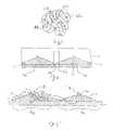
- a lithographic systemin accordance with an embodiment of the present invention includes a substrate 10 , having a substantially planar region shown as surface 12 . Disposed opposite substrate 10 is an imprint device 14 having a plurality of features thereon, forming a plurality of spaced-apart stepped-recesses 16 separated by a groove 18 , which should be deeper than stepped-recesses 16 , typically 10-20 ⁇ m. Although two stepped-recessed regions 16 are shown, any number may be present. The stepped recesses 16 extend parallel to groove 18 .
- a translation device 20is connected between imprint device 14 and substrate 10 to vary a distance “d” between imprint device 14 and substrate 10 .
- a radiation source 22is located so that imprint device 14 is positioned between radiation source 22 and substrate 10 .
- Radiation source 22is configured to impinge radiation on substrate 10 .
- imprint device 14is fabricated from material that allows it to be substantially transparent to the radiation produced by radiation source 22 .
- an imprint layer 24is disposed adjacent to surface 12 , between substrate 10 and imprint device 14 .
- imprint layer 24may be deposited using any known technique, in the present embodiment, imprint layer 24 is deposited as a plurality of spaced-apart discrete beads 25 of material 25 a on substrate 10 , discussed more fully below.
- Imprint layer 24is formed from a material 25 a that may be selectively polymerized and cross-linked to record a desired pattern. Material 25 a is shown in FIG. 3 as being cross-linked at points 25 b , forming cross-linked polymer material 25 c.
- the pattern recorded by imprint layer 24is produced, in part, by mechanical contact with imprint device 14 .
- translation device 20reduces the distance “d” to allow imprint layer 24 to come into mechanical contact with imprint device 14 , spreading beads 25 so as to form imprint layer 24 with a contiguous formation of material 25 a over regions 12 a of surface 12 , which are in superimposition with stepped-recesses 16 .
- a region 12 b of surface 12 in superimposition with groove 18is devoid of material 25 a .
- material 25 ais provided with the requisite viscosity to completely fill stepped-recesses 16 in a timely manner, while covering regions 12 a of surface 12 with a contiguous formation of material 25 a , on the order of a few milliseconds to a few seconds.
- sub-portions 24 a of imprint layer 24 coextensive with regions 12 ahave a stepped profile and are separated from adjacent sub-portions 24 a by hiatus 26 , after distance “d” has reached a desired distance, usually a minimum distance. After a desired distance “d” has been reached, radiation source 22 produces actinic radiation that polymerizes and cross-links material 25 a , forming cross-link polymer material 25 c , shown in FIG. 3.
- an exemplary radiation source 22may produce ultraviolet radiation.
- Other radiation sourcesmay be employed, such as thermal, electromagnetic and the like.
- the selection of radiation employed to initiate the polymerization of the material in imprint layer 24is known to one skilled in the art and typically depends on the specific application that is desired.
- translation device 20increases the distance “d” so that imprint device 14 and imprint layer 24 are spaced-apart.
- additional processingmay be employed to complete the patterning of substrate 10 .
- substrate 10 and imprint layer 24may be etched to remove residual material (not shown) present on imprint layer 24 after patterning has been completed.
- Residual materialmay consist of un-polymerized material 25 a , solid polymerized and cross-linked material 25 c , substrate 10 or a combination thereof.
- Well known etching processesmay be employed to that end, e.g., argon ion milling, a plasma etch, reactive ion etching or a combination thereof.
- removal of residual materialmay be accomplished during any stage of the patterning. For example, removal of residual material (not shown) may be carried out before etching the polymerized and cross-linked material 25 c.
- polymerization of material 25 asolidifies the surface of sub-portions regions 24 a with a shape conforming to a shape of stepped-recesses 16 .
- Thisprovides sub-portions 24 a with multiple steps, s 1 -s 14 having differing thicknesses, with thickness being measured in a direction parallel to distance “d”.
- Material 25 ais selected so that steps s 1 -s 14 define an optical coupling device 28 that propagates optical energy impinging thereupon after polymerization into material 25 c .
- optical energymay impinge upon surface 29 and propagate outwardly away from optical coupling device 28 through the surfaces associated with steps s 1 -s 14 .
- optical coupling device 28which includes sub-portions 24 a and regions 10 a of substrate 10 that are coextensive with regions 12 a , shown in FIG. 4, should be formed with material that is transparent to desired optical frequencies.
- An exemplary embodimentforms optical coupling device 28 from materials that facilitates propagation of optical energy in a range of 850 nm to 1,550 nm.
- the materialsshould demonstrate operational characteristics so as to withstand various environmental stresses without varying the optical properties of the optical coupling device 28 by, for example, 5 to 10%.
- optical coupling device 28should satisfy another operational characteristic that optical coupling device 28 should satisfy. To that end, optical coupling device 28 should withstand thermal cycling without cracking. Thus, for a given material from which substrate 10 is formed, material 25 c should maintain structural integrity when subjected changes in the ambient temperature, e.g., 0° C. to 70° C. in which optical coupling device 28 is employed. Material 25 c should also maintain structural integrity when subjected to temperature changes due to the periodicity at which optical energy impinges upon optical coupling device 28 , as well as, differences in coefficient of thermal expansion ( ⁇ CTE) of material 25 c from which optical coupling device 28 is formed and the material from which substrate 10 is formed.
- ⁇ CTEcoefficient of thermal expansion
- material 25 ais deposited on substrate 10 as a plurality of discrete and spaced-apart beads 25 .
- the combined volume of beads 25is such that the material 25 a is distributed appropriately over an area of regions 12 a , while avoiding the presence of material in region 12 b .
- imprint layer 24is spread and patterned concurrently, with the pattern being subsequently set by exposure to actinic radiation, such as ultraviolet radiation.
- material 25 ahave certain processing characteristics to facilitate rapid and even spreading of material 25 a in beads 25 over regions 12 a while avoiding the presence of material 25 a in region 12 b.
- the desirable processing characteristicsinclude having a viscosity approximately that of water, (H 2 O), 1 to 2 centepoise (csp), or in some cases as high as 20-50 cps, dependent upon the lateral dimensions of the features, as well as the ability to wet surface of substrate 10 to avoid subsequent pit or hole formation after polymerization.
- the wettability of imprint layer 24should be such that the angle, ⁇ 1 , is defined as follows:
- imprint layer 24may be made sufficiently thin while avoiding formation of pits or holes in the thinner regions.
- optical coupling device 28another desirable characteristic that it is desired for material 25 a to possess is thermal stability during further manufacturing processes and post process testing. To that end, it is desired that the structural integrity of optical coupling device 28 be maintained when subjected to wave soldering at 260° C. for ninety (90) seconds, e.g., three (3) intervals at thirty (30) seconds per interval. Additionally, it is desirous to have optical coupling device 28 maintain structural integrity when subjected to thermal cycling between ⁇ 40° to 100° C. with a fifteen (15) minute dwell time at the endpoints of the temperature ranges and a five (5) minute transition time between temperatures.
- optical coupling device 28maintain structural integrity when subjected to an 85° C. ambient of 85% humidity for 1,000 hours. It is further desired that the wetting of imprint device 14 by imprint layer 24 be minimized. To that end, the wetting angle, ⁇ 2 , should be greater than 75°.
- substrate 10may be formed from a number of different materials.
- substrate 10may be formed from silica, polymers, cadmium telluride, quartz and virtually any other electro-optic material.
- substrate 10may include one or more layers in regions 12 a , discussed more fully below.
- the constituent components of material 25 aconsist of acrylated polymerizable compositions and an initiator.
- the polymerizable compositionsare selected to provide material 25 a with a minimal viscosity, e.g., viscosity approximating the viscosity of water (1-2 cps) or up to 10-50 cps, and to provide the aforementioned operational and process characteristics.
- the initiatoris provided to produce a free radical reaction in response to actinic radiation, causing the polymerizable compositions to polymerize and cross-link, forming cross-linked polymer material 25 c .
- a photo-initiator responsive to ultraviolet radiationis employed.
- polymerizable compositionsinclude, but are not limited to, ethylene diol diacrylate, t-butyl acrylate, bisphenol A diacrylate, acrylate terminated polysiloxane, as well as compositions thereof.
- Other acrylatesmay also include fluorinated acrylates as described by Blomquist et al. in the article entitled FLUORINATED ACRYLATES IN MAKING LOW-LOSS, LOW-BIREFRINGENCE, AND SINGLE-MODE OPTICAL WAVEGUIDES WITH EXCEPTIONAL THERMO-OPTIC PROPERTIES, SPIE Vol. 3799, pp. 266-279 (1999).
- the fluorinated acrylatesinclude polydifluoromethylene diacrylates, perfluoropolyether diacrylates and chlorofluorodiacrylates.
- the initiatormay be any component that initiates a free radical reaction in response to radiation, produced by radiation source 22 , shown in FIG. 1, impinging thereupon and being absorbed thereby. Suitable initiators may include, but are not limited to, photo-initiators such as 1-hydroxycyclohexyl phenyl ketone or phenylbis(2,4,6-trimethyl benzoyl) phosphine oxide.
- the initiatormay be present in material 25 a in amounts of up to 5% by weight, but is typically present in an amount of 2-4% by weight.
- suitable silylated polymerizable compositionsmay include, but are not limited to, 1,3-bis(3-methacryloxypropyl)tetramethyldisiloxane, (3-acryloxypropyl)tris(tri-methoxysiloxy)-silane.
- compositions that material 25 amay consist of include epoxies, such as cyclo aliphatic epoxies.
- epoxiessuch as cyclo aliphatic epoxies.
- An exemplary cyclo aliphatic epoxythat may demonstrate the aforementioned operational and process characteristics is available from Union Carbide as part number ERL 4221.
- vinyl ethersmay demonstrate the aforementioned operational and process characteristics, e.g., polyvinyl ether and copolymers, such as isobutyl ethers used in conjunction with acrylics.
- compositions for material 25 aare as follows:
- compositionscould vary by as much as 20%, dependent upon the stoichiometry.
- the above-identified compositionsmay also include stabilizers that are well known in the chemical art to increase the operational life, as well as initiators.
- an optical coupling device 128that includes a stress relief layer 130 disposed between substrate 110 and sub-portions 124 a .
- Stress relief layer 130increases the selection of materials that may be employed to form optical coupling device 128 .
- stress relief layer 130typically has a classification temperature Tg that is lower than the operational temperature of optical coupling device 128 . This allows the use of materials having a Tg that is higher than the operational temperature of optical coupling device 128 without exacerbating the probability of cracking, because of the flexibility introduced by the presence of stress relief layer 130 .
- stress relief layer 130may be formed from polysiloxane rubbers, with an acrylic end group attached thereto to facilitate cross-linking when exposed to ultraviolet radiation.
- the polysiloxane rubbermay be thermally cross-linked.
- Stress relief layer 130may be disposed upon substrate 110 using spin-on techniques. It is desired that the material from which stress relief layer 130 is formed does not swell in acrylate polymerizable compositions. As a result, fluorosilocane rubbers may be beneficial to include in stress relief layer.
- stress relief layer 130may function as a planarization layer. As a result, stress relief layer 130 may provide an additional function of ensuring surface 112 is planar. To that end, stress relief layer 130 may be fabricated in such a manner so as to possess a continuous, smooth, relatively defect-free surface that may exhibit excellent adhesion to sub-portions 124 a.
- imprint device 14may be treated with a modifying agent.
- a modifying agentis a release layer (not shown) formed from a fluorocarbon silylating agent.
- Release layer (not shown) and other surface modifying agentsmay be applied using any known process. For example, processing techniques that may include chemical vapor deposition method, physical vapor deposition, atomic layer deposition or various other techniques, brazing and the like.
- imprint layer 24is located between substrate 10 and release layer (not shown), during imprint lithography processes.
Landscapes
- Engineering & Computer Science (AREA)
- Physics & Mathematics (AREA)
- Chemical & Material Sciences (AREA)
- Nanotechnology (AREA)
- General Physics & Mathematics (AREA)
- Crystallography & Structural Chemistry (AREA)
- Manufacturing & Machinery (AREA)
- Condensed Matter Physics & Semiconductors (AREA)
- Mathematical Physics (AREA)
- Theoretical Computer Science (AREA)
- Microelectronics & Electronic Packaging (AREA)
- Optics & Photonics (AREA)
- Shaping Of Tube Ends By Bending Or Straightening (AREA)
Abstract
Description
- The field of invention relates generally to micro-fabrication of structures. More particularly, the present invention is directed to a functional patterning material suited for use in imprint lithographic processes to form optical components.[0001]
- Optical communication systems include numerous optical devices, such as planar optical slab waveguides, channel optical waveguides, rib waveguides, optical couplers, optical splitters, optical switches, micro-optical elements and the like. Many of these optical devices are employed using standard photolithographic processes. As a result, many photopolymers have been developed. The photopolymers, such as acrylate materials, are light sensitive to facilitate recordation of a pattern therein. Furthermore, the photopolymers must demonstrate suitable operational and process characteristics. For example, it is desired that the photopolymers have good clarity and low birefringence over a range of temperatures. As a result, the thermal stability of the photopolymers is an important factor and should be such that the probability of color changes in the photopolymers is minimized during prolonged operation. Additionally, the photopolymers should withstand stresses so as not to crack during the baking process or during use. Finally, maximizing the miniaturization of the optical devices is desired. Recent advances in micro-fabrication techniques, have showed promising results in miniaturizing optical devices.[0002]
- An exemplary micro-fabrication technique, commonly referred to as imprint lithography, is shown in U.S. Pat. No. 6,334,960 to Willson et al. Willson et al. disclose a method of forming a relief image in a structure. The method includes providing a substrate having a transfer layer. The transfer layer is covered with a polymerizable fluid composition. A mold makes mechanical contact with the polymerizable fluid. The mold includes a relief structure, and the polymerizable fluid composition fills the relief structure. The polymerizable fluid composition is then subjected to conditions to solidify and polymerize the same, forming a solidified polymeric material on the transfer layer that contains a relief structure complimentary to that of the mold. The mold is then separated from the solid polymeric material such that a replica of the relief structure in the mold is formed in the solidified polymeric material. The transfer layer and the solidified polymeric material are subjected to an environment to selectively etch the transfer layer relative to the solidified polymeric material such that a relief image is formed in the transfer layer. The time required and the minimum feature dimension provided by this technique is dependent upon, inter alia, the composition of the polymerizable material. However, Willson et al. does not disclose material suitable for use in forming optical devices employed in communication systems that may be formed using imprint lithography.[0003]
- It is desired, therefore, to provide techniques to form optical devices using imprint lithographic processes.[0004]
- The present invention includes a method for forming an optical coupling device on a substrate by disposing a material onto the substrate that is polymerizable in response to actinic radiation. A stack of the material is formed by contacting the material with a template having a stepped-recess formed therein. The material is then solidified into an optically transparent body with a surface having a plurality of steps by subjecting the stack to actinic radiation. To that end, the material may comprise a polymerizable acrylate component selected from a set of acrylates consisting essentially of ethylene di diacrylate, t-butyl acrylate, bisphenol A diacrylate, acrylate terminated polysiloxane, polydifluoromethylene diacrylate, perfluoropolyether diacrylates and chlorofluorodiacrylates. Alternatively, the material may include a silylated component selected from a group consisting essentially of (3-acryloxypropyltristrimethylsiloxy) silane. In yet another embodiment of the present invention, a stress relief layer may be disposed on the substrate before formation of the stack to reduce the probability of the stack cracking during operation. Thereafter, the material may be disposed on the stress relief layer. One embodiment of the stress relief layer may be formed from rubbers, such as polysiloxane rubber and fluorosilocane rubber. These and other embodiments are described herein.[0005]
- FIG. 1 is a simplified elevation view of a lithographic system in accordance with the present invention;[0006]
- FIG. 2 is a simplified representation of material from which an imprint layer, shown in FIG. 1, is comprised before being polymerized and cross-linked;[0007]
- FIG. 3 is a simplified representation of cross-linked polymer material into which the material shown in FIG. 2 is transformed after being subjected to radiation;[0008]
- FIG. 4 is a simplified elevation view of an imprint device, shown in FIG. 1, in mechanical contact with an imprint layer disposed on a substrate, in accordance with one embodiment of the present invention;[0009]
- FIG. 5 is a simplified elevation view of the imprint layer, shown in FIG. 4, after patterning; and[0010]
- FIG. 6 is a simplified elevation view of material in an imprint device and substrate employed with the present invention in accordance with an alternate embodiment.[0011]
- Referring to FIG. 1, a lithographic system in accordance with an embodiment of the present invention includes a[0012]
substrate 10, having a substantially planar region shown assurface 12. Disposedopposite substrate 10 is animprint device 14 having a plurality of features thereon, forming a plurality of spaced-apart stepped-recesses 16 separated by agroove 18, which should be deeper than stepped-recesses 16, typically 10-20 μm. Although two stepped-recessed regions 16 are shown, any number may be present. Thestepped recesses 16 extend parallel togroove 18. Atranslation device 20 is connected betweenimprint device 14 andsubstrate 10 to vary a distance “d” betweenimprint device 14 andsubstrate 10. Aradiation source 22 is located so thatimprint device 14 is positioned betweenradiation source 22 andsubstrate 10.Radiation source 22 is configured to impinge radiation onsubstrate 10. To realize this,imprint device 14 is fabricated from material that allows it to be substantially transparent to the radiation produced byradiation source 22. - Referring to both FIGS. 1 and 2, an[0013]
imprint layer 24 is disposed adjacent tosurface 12, betweensubstrate 10 andimprint device 14. Althoughimprint layer 24 may be deposited using any known technique, in the present embodiment,imprint layer 24 is deposited as a plurality of spaced-apartdiscrete beads 25 of material25aonsubstrate 10, discussed more fully below.Imprint layer 24 is formed from a material25athat may be selectively polymerized and cross-linked to record a desired pattern. Material25ais shown in FIG. 3 as being cross-linked atpoints 25b, formingcross-linked polymer material 25c. - Referring to FIGS. 1, 2 and[0014]4, the pattern recorded by
imprint layer 24 is produced, in part, by mechanical contact withimprint device 14. To that end,translation device 20 reduces the distance “d” to allowimprint layer 24 to come into mechanical contact withimprint device 14, spreadingbeads 25 so as to formimprint layer 24 with a contiguous formation of material25aover regions12aofsurface 12, which are in superimposition with stepped-recesses 16. A region12bofsurface 12 in superimposition withgroove 18 is devoid of material25a. This occurs by providingbeads 25 with a requisite volume so that stepped-recesses 16 become filled, but, due to capillary action, material from whichbeads 25 are formed does not entergroove 18. As a result, the material ofbeads 25 are provided with the requisite viscosity that may vary, dependent, inter alia, upon the size ofgroove 18, stepped-recess16 and distance “d”. As a result there is a discontinuity, orhiatus 26, inlayer 24. In one embodiment, distance “d” is reduced to allowsub-portions 24aofimprint layer 24 to ingress into and fill stepped-recesses 16, while avoiding filling ofgroove 18. - To facilitate filling of stepped-[0015]
recesses 16 and avoiding the presence of material25ainhiatus 26, material25ais provided with the requisite viscosity to completely fill stepped-recesses 16 in a timely manner, while covering regions12aofsurface 12 with a contiguous formation of material25a, on the order of a few milliseconds to a few seconds. In the present embodiment,sub-portions 24aofimprint layer 24 coextensive with regions12ahave a stepped profile and are separated fromadjacent sub-portions 24abyhiatus 26, after distance “d” has reached a desired distance, usually a minimum distance. After a desired distance “d” has been reached,radiation source 22 produces actinic radiation that polymerizes and cross-links material25a, formingcross-link polymer material 25c, shown in FIG. 3. - Referring to FIGS. 1 and 3, an[0016]
exemplary radiation source 22 may produce ultraviolet radiation. Other radiation sources may be employed, such as thermal, electromagnetic and the like. The selection of radiation employed to initiate the polymerization of the material inimprint layer 24 is known to one skilled in the art and typically depends on the specific application that is desired. Afterimprint layer 24 is transformed to consist ofmaterial 25c,translation device 20 increases the distance “d” so thatimprint device 14 andimprint layer 24 are spaced-apart. - Referring to FIGS. 1, 2 and[0017]3, additional processing may be employed to complete the patterning of
substrate 10. For example,substrate 10 andimprint layer 24 may be etched to remove residual material (not shown) present onimprint layer 24 after patterning has been completed. Residual material (not shown) may consist of un-polymerized material25a, solid polymerized andcross-linked material 25c,substrate 10 or a combination thereof. Well known etching processes may be employed to that end, e.g., argon ion milling, a plasma etch, reactive ion etching or a combination thereof. Further, removal of residual material (not shown) may be accomplished during any stage of the patterning. For example, removal of residual material (not shown) may be carried out before etching the polymerized andcross-linked material 25c. - Referring to FIGS. 2, 3, and[0018]5, polymerization of material25asolidifies the surface of
sub-portions regions 24awith a shape conforming to a shape of stepped-recesses 16. This provides sub-portions24awith multiple steps, s1-s14having differing thicknesses, with thickness being measured in a direction parallel to distance “d”. Material25ais selected so that steps s1-s14define anoptical coupling device 28 that propagates optical energy impinging thereupon after polymerization intomaterial 25c. For example, optical energy may impinge upon surface29 and propagate outwardly away fromoptical coupling device 28 through the surfaces associated with steps s1-s14. - As a result,[0019]
optical coupling device 28, which includes sub-portions24aand regions10aofsubstrate 10 that are coextensive with regions12a, shown in FIG. 4, should be formed with material that is transparent to desired optical frequencies. An exemplary embodiment formsoptical coupling device 28 from materials that facilitates propagation of optical energy in a range of 850 nm to 1,550 nm. In addition, the materials should demonstrate operational characteristics so as to withstand various environmental stresses without varying the optical properties of theoptical coupling device 28 by, for example, 5 to 10%. - Another operational characteristic that[0020]
optical coupling device 28 should satisfy is maintaining structural integrity during operation. To that end,optical coupling device 28 should withstand thermal cycling without cracking. Thus, for a given material from whichsubstrate 10 is formed,material 25cshould maintain structural integrity when subjected changes in the ambient temperature, e.g., 0° C. to 70° C. in whichoptical coupling device 28 is employed.Material 25cshould also maintain structural integrity when subjected to temperature changes due to the periodicity at which optical energy impinges uponoptical coupling device 28, as well as, differences in coefficient of thermal expansion (ΔCTE) ofmaterial 25cfrom whichoptical coupling device 28 is formed and the material from whichsubstrate 10 is formed. - Referring to FIGS. 1, 2,[0021]3 and4, in addition to the operational characteristics that
material 25cshould satisfy, it is desirous to have material25asatisfy numerous processing characteristics considering the unique deposition process employed. As mentioned above, material25ais deposited onsubstrate 10 as a plurality of discrete and spaced-apartbeads 25. The combined volume ofbeads 25 is such that the material25ais distributed appropriately over an area of regions12a, while avoiding the presence of material in region12b. As a result,imprint layer 24 is spread and patterned concurrently, with the pattern being subsequently set by exposure to actinic radiation, such as ultraviolet radiation. Thus, in addition to the operational characteristics mentioned above, it is desired that material25ahave certain processing characteristics to facilitate rapid and even spreading of material25ainbeads 25 over regions12awhile avoiding the presence of material25ain region12b. - The desirable processing characteristics include having a viscosity approximately that of water, (H[0022]2O), 1 to 2 centepoise (csp), or in some cases as high as 20-50 cps, dependent upon the lateral dimensions of the features, as well as the ability to wet surface of
substrate 10 to avoid subsequent pit or hole formation after polymerization. To that end, in one example, the wettability ofimprint layer 24, as defined by the contact angle method, should be such that the angle, θ1, is defined as follows: - 0≧θ1<75°
- With these two characteristics being satisfied,[0023]
imprint layer 24 may be made sufficiently thin while avoiding formation of pits or holes in the thinner regions. - Referring to FIGS. 1, 2,[0024]3 and5, another desirable characteristic that it is desired for material25ato possess is thermal stability during further manufacturing processes and post process testing. To that end, it is desired that the structural integrity of
optical coupling device 28 be maintained when subjected to wave soldering at 260° C. for ninety (90) seconds, e.g., three (3) intervals at thirty (30) seconds per interval. Additionally, it is desirous to haveoptical coupling device 28 maintain structural integrity when subjected to thermal cycling between −40° to 100° C. with a fifteen (15) minute dwell time at the endpoints of the temperature ranges and a five (5) minute transition time between temperatures. Finally, it is desirous to haveoptical coupling device 28 maintain structural integrity when subjected to an 85° C. ambient of 85% humidity for 1,000 hours. It is further desired that the wetting ofimprint device 14 byimprint layer 24 be minimized. To that end, the wetting angle, θ2, should be greater than 75°. - Referring to FIGS. 2 and 4, the constituent components that form material[0025]25ato provide the aforementioned operational and process characteristics may differ. This results from
substrate 10 being formed from a number of different materials. For example,substrate 10 may be formed from silica, polymers, cadmium telluride, quartz and virtually any other electro-optic material. Additionally,substrate 10 may include one or more layers in regions12a, discussed more fully below. - Referring to FIGS. 2 and 3, in one embodiment of the present invention the constituent components of material[0026]25aconsist of acrylated polymerizable compositions and an initiator. The polymerizable compositions are selected to provide material25awith a minimal viscosity, e.g., viscosity approximating the viscosity of water (1-2 cps) or up to 10-50 cps, and to provide the aforementioned operational and process characteristics. The initiator is provided to produce a free radical reaction in response to actinic radiation, causing the polymerizable compositions to polymerize and cross-link, forming
cross-linked polymer material 25c. In the present example, a photo-initiator responsive to ultraviolet radiation is employed. - Examples of polymerizable compositions include, but are not limited to, ethylene diol diacrylate, t-butyl acrylate, bisphenol A diacrylate, acrylate terminated polysiloxane, as well as compositions thereof. Other acrylates may also include fluorinated acrylates as described by Blomquist et al. in the article entitled FLUORINATED ACRYLATES IN MAKING LOW-LOSS, LOW-BIREFRINGENCE, AND SINGLE-MODE OPTICAL WAVEGUIDES WITH EXCEPTIONAL THERMO-OPTIC PROPERTIES, SPIE Vol. 3799, pp. 266-279 (1999). Examples of the fluorinated acrylates include polydifluoromethylene diacrylates, perfluoropolyether diacrylates and chlorofluorodiacrylates. The initiator may be any component that initiates a free radical reaction in response to radiation, produced by[0027]
radiation source 22, shown in FIG. 1, impinging thereupon and being absorbed thereby. Suitable initiators may include, but are not limited to, photo-initiators such as 1-hydroxycyclohexyl phenyl ketone or phenylbis(2,4,6-trimethyl benzoyl) phosphine oxide. The initiator may be present in material25ain amounts of up to 5% by weight, but is typically present in an amount of 2-4% by weight. Were it desired to include silylated polymerizable compositions in material25a, suitable silylated polymerizable compositions may include, but are not limited to, 1,3-bis(3-methacryloxypropyl)tetramethyldisiloxane, (3-acryloxypropyl)tris(tri-methoxysiloxy)-silane. - Other compositions that material[0028]25amay consist of include epoxies, such as cyclo aliphatic epoxies. An exemplary cyclo aliphatic epoxy that may demonstrate the aforementioned operational and process characteristics is available from Union Carbide as part number ERL 4221. Additionally some vinyl ethers may demonstrate the aforementioned operational and process characteristics, e.g., polyvinyl ether and copolymers, such as isobutyl ethers used in conjunction with acrylics.
- Specific examples of compositions for material[0029]25aare as follows:
- It should be understood that the relative mixture between the non-initiator components of the aforementioned compositions could vary by as much as 20%, dependent upon the stoichiometry. Also, the above-identified compositions may also include stabilizers that are well known in the chemical art to increase the operational life, as well as initiators.[0030]
- Referring to FIG. 6, another embodiment in accordance with the present invention provides an[0031]
optical coupling device 128 that includes astress relief layer 130 disposed between substrate110 and sub-portions124a.Stress relief layer 130 increases the selection of materials that may be employed to formoptical coupling device 128. Specifically,stress relief layer 130 typically has a classification temperature Tg that is lower than the operational temperature ofoptical coupling device 128. This allows the use of materials having a Tg that is higher than the operational temperature ofoptical coupling device 128 without exacerbating the probability of cracking, because of the flexibility introduced by the presence ofstress relief layer 130. To providestress relief layer 130 with optical transparence to the radiation that will be used during operation,stress relief layer 130 may be formed from polysiloxane rubbers, with an acrylic end group attached thereto to facilitate cross-linking when exposed to ultraviolet radiation. Alternatively, the polysiloxane rubber may be thermally cross-linked.Stress relief layer 130 may be disposed upon substrate110 using spin-on techniques. It is desired that the material from whichstress relief layer 130 is formed does not swell in acrylate polymerizable compositions. As a result, fluorosilocane rubbers may be beneficial to include in stress relief layer. - Referring to FIGS. 2 and 6, an additional benefit provide by[0032]
stress relief layer 130 is that the same may function as a planarization layer. As a result,stress relief layer 130 may provide an additional function of ensuringsurface 112 is planar. To that end,stress relief layer 130 may be fabricated in such a manner so as to possess a continuous, smooth, relatively defect-free surface that may exhibit excellent adhesion to sub-portions124a. - Referring again to FIG. 1, to ensure that[0033]
imprint layer 24 does not adhere toimprint device 14,imprint device 14 may be treated with a modifying agent. One such modifying agent is a release layer (not shown) formed from a fluorocarbon silylating agent. Release layer (not shown) and other surface modifying agents, may be applied using any known process. For example, processing techniques that may include chemical vapor deposition method, physical vapor deposition, atomic layer deposition or various other techniques, brazing and the like. In this configuration,imprint layer 24 is located betweensubstrate 10 and release layer (not shown), during imprint lithography processes. - The embodiments of the present invention described above are exemplary. Many changes and modifications may be made to the disclosure recited above, while remaining within the scope of the invention. For example, although the present embodiment is discussed with respect to having fourteen steps, any number of steps may be formed. The scope of the invention should, therefore, be determined not with reference to the above description, but instead with reference to the appended claims along with their full scope of equivalents.[0034]
Claims (22)
Priority Applications (1)
| Application Number | Priority Date | Filing Date | Title |
|---|---|---|---|
| US10/235,314US6936194B2 (en) | 2002-09-05 | 2002-09-05 | Functional patterning material for imprint lithography processes |
Applications Claiming Priority (1)
| Application Number | Priority Date | Filing Date | Title |
|---|---|---|---|
| US10/235,314US6936194B2 (en) | 2002-09-05 | 2002-09-05 | Functional patterning material for imprint lithography processes |
Publications (2)
| Publication Number | Publication Date |
|---|---|
| US20040046271A1true US20040046271A1 (en) | 2004-03-11 |
| US6936194B2 US6936194B2 (en) | 2005-08-30 |
Family
ID=31990498
Family Applications (1)
| Application Number | Title | Priority Date | Filing Date |
|---|---|---|---|
| US10/235,314Expired - Fee RelatedUS6936194B2 (en) | 2002-09-05 | 2002-09-05 | Functional patterning material for imprint lithography processes |
Country Status (1)
| Country | Link |
|---|---|
| US (1) | US6936194B2 (en) |
Cited By (47)
| Publication number | Priority date | Publication date | Assignee | Title |
|---|---|---|---|---|
| US20030235787A1 (en)* | 2002-06-24 | 2003-12-25 | Watts Michael P.C. | Low viscosity high resolution patterning material |
| US20040065976A1 (en)* | 2002-10-04 | 2004-04-08 | Sreenivasan Sidlgata V. | Method and a mold to arrange features on a substrate to replicate features having minimal dimensional variability |
| US20040089979A1 (en)* | 2002-11-13 | 2004-05-13 | Molecular Imprints, Inc. | Method of reducing pattern distortions during imprint lithography processes |
| US20040124566A1 (en)* | 2002-07-11 | 2004-07-01 | Sreenivasan Sidlgata V. | Step and repeat imprint lithography processes |
| US20050028618A1 (en)* | 2002-12-12 | 2005-02-10 | Molecular Imprints, Inc. | System for determining characteristics of substrates employing fluid geometries |
| US20050067379A1 (en)* | 2003-09-25 | 2005-03-31 | Molecular Imprints, Inc. | Imprint lithography template having opaque alignment marks |
| US20050084804A1 (en)* | 2003-10-16 | 2005-04-21 | Molecular Imprints, Inc. | Low surface energy templates |
| US20050192421A1 (en)* | 2004-02-27 | 2005-09-01 | Molecular Imprints, Inc. | Composition for an etching mask comprising a silicon-containing material |
| US20050236739A1 (en)* | 1999-03-11 | 2005-10-27 | Board Of Regents, The University Of Texas System | Step and flash imprint lithography |
| US20050276919A1 (en)* | 2004-06-01 | 2005-12-15 | Molecular Imprints, Inc. | Method for dispensing a fluid on a substrate |
| WO2005119395A2 (en) | 2004-06-01 | 2005-12-15 | Molecular Imprints, Inc. | Method and system to control movement of a body for nano-scale manufacturing |
| US20060035029A1 (en)* | 2004-08-16 | 2006-02-16 | Molecular Imprints, Inc. | Method to provide a layer with uniform etch characteristics |
| US20060062922A1 (en)* | 2004-09-23 | 2006-03-23 | Molecular Imprints, Inc. | Polymerization technique to attenuate oxygen inhibition of solidification of liquids and composition therefor |
| US20060081557A1 (en)* | 2004-10-18 | 2006-04-20 | Molecular Imprints, Inc. | Low-k dielectric functional imprinting materials |
| US20060096477A1 (en)* | 2002-09-09 | 2006-05-11 | Alexander Bietsch | Printing in a medium |
| US20060108710A1 (en)* | 2004-11-24 | 2006-05-25 | Molecular Imprints, Inc. | Method to reduce adhesion between a conformable region and a mold |
| WO2006057843A2 (en) | 2004-11-24 | 2006-06-01 | Molecular Imprints, Inc. | Method and composition providing desirable characteristics between a mold and a polymerizable composition |
| US20060145398A1 (en)* | 2004-12-30 | 2006-07-06 | Board Of Regents, The University Of Texas System | Release layer comprising diamond-like carbon (DLC) or doped DLC with tunable composition for imprint lithography templates and contact masks |
| US20060172031A1 (en)* | 2005-01-31 | 2006-08-03 | Molecular Imprints, Inc. | Chucking system for nano-manufacturing |
| US7122482B2 (en) | 2003-10-27 | 2006-10-17 | Molecular Imprints, Inc. | Methods for fabricating patterned features utilizing imprint lithography |
| US7157036B2 (en) | 2003-06-17 | 2007-01-02 | Molecular Imprints, Inc | Method to reduce adhesion between a conformable region and a pattern of a mold |
| US20070051697A1 (en)* | 2005-09-02 | 2007-03-08 | Dipietro Richard A | Processes and materials for step and flash imprint lithography |
| US20070063384A1 (en)* | 2005-09-21 | 2007-03-22 | Molecular Imprints, Inc. | Method to control an atmostphere between a body and a substrate |
| US20070264481A1 (en)* | 2003-12-19 | 2007-11-15 | Desimone Joseph M | Isolated and fixed micro and nano structures and methods thereof |
| US20070264591A1 (en)* | 2006-05-15 | 2007-11-15 | Asml Netherlands B.V. | Imprint lithography |
| US20070264833A1 (en)* | 2006-05-11 | 2007-11-15 | Hitachi Global Storage Technologies | High resolution patterning of surface energy utilizing high resolution monomolecular resist for fabrication of patterned media masters |
| US20070275193A1 (en)* | 2004-02-13 | 2007-11-29 | Desimone Joseph M | Functional Materials and Novel Methods for the Fabrication of Microfluidic Devices |
| US20080181958A1 (en)* | 2006-06-19 | 2008-07-31 | Rothrock Ginger D | Nanoparticle fabrication methods, systems, and materials |
| US20090027603A1 (en)* | 2005-02-03 | 2009-01-29 | Samulski Edward T | Low Surface Energy Polymeric Material for Use in Liquid Crystal Displays |
| US20090028910A1 (en)* | 2003-12-19 | 2009-01-29 | University Of North Carolina At Chapel Hill | Methods for Fabrication Isolated Micro-and Nano-Structures Using Soft or Imprint Lithography |
| US20090165320A1 (en)* | 2003-09-23 | 2009-07-02 | Desimone Joseph M | Photocurable perfluoropolyethers for use as novel materials in microfluidic devices |
| US7604836B2 (en) | 2006-12-13 | 2009-10-20 | Hitachi Global Storage Technologies Netherlands B.V. | Release layer and resist material for master tool and stamper tool |
| US20090272875A1 (en)* | 2003-06-17 | 2009-11-05 | Molecular Imprints, Inc. | Composition to Reduce Adhesion Between a Conformable Region and a Mold |
| US20090274874A1 (en)* | 2008-04-30 | 2009-11-05 | Zhiyong Li | Photonic Device And Method For Forming Nano-Structures |
| US20090304992A1 (en)* | 2005-08-08 | 2009-12-10 | Desimone Joseph M | Micro and Nano-Structure Metrology |
| US20100109195A1 (en)* | 2008-11-05 | 2010-05-06 | Molecular Imprints, Inc. | Release agent partition control in imprint lithography |
| US20100151031A1 (en)* | 2007-03-23 | 2010-06-17 | Desimone Joseph M | Discrete size and shape specific organic nanoparticles designed to elicit an immune response |
| US20100193993A1 (en)* | 2007-06-27 | 2010-08-05 | Agency For Science, Technology And Research | Method of making a secondary imprint on an imprinted polymer |
| US7837921B2 (en) | 2004-01-23 | 2010-11-23 | Molecular Imprints, Inc. | Method of providing desirable wetting and release characteristics between a mold and a polymerizable composition |
| EP2267531A2 (en) | 2004-06-03 | 2010-12-29 | Molecular Imprints, Inc. | Method to vary dimensions of a substrate during nano-scale manufacturing |
| US20110165412A1 (en)* | 2009-11-24 | 2011-07-07 | Molecular Imprints, Inc. | Adhesion layers in nanoimprint lithograhy |
| US8142703B2 (en) | 2005-10-05 | 2012-03-27 | Molecular Imprints, Inc. | Imprint lithography method |
| US8158728B2 (en) | 2004-02-13 | 2012-04-17 | The University Of North Carolina At Chapel Hill | Methods and materials for fabricating microfluidic devices |
| US20140010960A1 (en)* | 2011-01-21 | 2014-01-09 | The University Of Tokyo | Method of producing microstructured gel |
| WO2017059445A1 (en)* | 2015-10-02 | 2017-04-06 | The Arizona Board Of Regents On Behalf Of The University Of Arizona | Fabrication of optical interconnect structures for a photonic integrated circuit |
| KR20180072553A (en)* | 2016-12-21 | 2018-06-29 | 캐논 가부시끼가이샤 | Template for imprint lithography including a recession and an apparatus and method of using the template |
| JP2019106514A (en)* | 2017-12-14 | 2019-06-27 | キヤノン株式会社 | Method for manufacturing cured product pattern, method for manufacturing processed substrate, method for manufacturing circuit board, method for manufacturing electronic components, and method for manufacturing imprint mold |
Families Citing this family (147)
| Publication number | Priority date | Publication date | Assignee | Title |
|---|---|---|---|---|
| CN1262883C (en) | 2000-07-17 | 2006-07-05 | 得克萨斯州大学系统董事会 | Method and system of automatic fluid dispensing for imprint lithography processes |
| US8294025B2 (en) | 2002-06-08 | 2012-10-23 | Solarity, Llc | Lateral collection photovoltaics |
| US20080160129A1 (en)* | 2006-05-11 | 2008-07-03 | Molecular Imprints, Inc. | Template Having a Varying Thickness to Facilitate Expelling a Gas Positioned Between a Substrate and the Template |
| US8076386B2 (en) | 2004-02-23 | 2011-12-13 | Molecular Imprints, Inc. | Materials for imprint lithography |
| US7906180B2 (en)* | 2004-02-27 | 2011-03-15 | Molecular Imprints, Inc. | Composition for an etching mask comprising a silicon-containing material |
| KR101193918B1 (en)* | 2004-06-03 | 2012-10-29 | 몰레큘러 임프린츠 인코퍼레이티드 | Fluid dispensing and drop-on-demand dispensing for nano-scale menufacturing |
| US7768624B2 (en) | 2004-06-03 | 2010-08-03 | Board Of Regents, The University Of Texas System | Method for obtaining force combinations for template deformation using nullspace and methods optimization techniques |
| US20070228593A1 (en)* | 2006-04-03 | 2007-10-04 | Molecular Imprints, Inc. | Residual Layer Thickness Measurement and Correction |
| SG147419A1 (en) | 2004-09-21 | 2008-11-28 | Molecular Imprints Inc | Method of forming an in-situ recessed structure |
| US7205244B2 (en) | 2004-09-21 | 2007-04-17 | Molecular Imprints | Patterning substrates employing multi-film layers defining etch-differential interfaces |
| US7636999B2 (en) | 2005-01-31 | 2009-12-29 | Molecular Imprints, Inc. | Method of retaining a substrate to a wafer chuck |
| US7635263B2 (en) | 2005-01-31 | 2009-12-22 | Molecular Imprints, Inc. | Chucking system comprising an array of fluid chambers |
| US8808808B2 (en)* | 2005-07-22 | 2014-08-19 | Molecular Imprints, Inc. | Method for imprint lithography utilizing an adhesion primer layer |
| US8846195B2 (en)* | 2005-07-22 | 2014-09-30 | Canon Nanotechnologies, Inc. | Ultra-thin polymeric adhesion layer |
| US7759407B2 (en) | 2005-07-22 | 2010-07-20 | Molecular Imprints, Inc. | Composition for adhering materials together |
| US8557351B2 (en)* | 2005-07-22 | 2013-10-15 | Molecular Imprints, Inc. | Method for adhering materials together |
| US7906058B2 (en) | 2005-12-01 | 2011-03-15 | Molecular Imprints, Inc. | Bifurcated contact printing technique |
| MY144847A (en) | 2005-12-08 | 2011-11-30 | Molecular Imprints Inc | Method and system for double-sided patterning of substrates |
| KR20080104292A (en)* | 2006-03-06 | 2008-12-02 | 아사히 가라스 가부시키가이샤 | Treating substrate having a hydrophilic region and a water-repellent region and a method for producing the same |
| US8142850B2 (en)* | 2006-04-03 | 2012-03-27 | Molecular Imprints, Inc. | Patterning a plurality of fields on a substrate to compensate for differing evaporation times |
| US8850980B2 (en)* | 2006-04-03 | 2014-10-07 | Canon Nanotechnologies, Inc. | Tessellated patterns in imprint lithography |
| US8215946B2 (en) | 2006-05-18 | 2012-07-10 | Molecular Imprints, Inc. | Imprint lithography system and method |
| JP2010537395A (en)* | 2007-05-30 | 2010-12-02 | モレキュラー・インプリンツ・インコーポレーテッド | Template with silicon nitride, silicon carbide, or silicon oxynitride film |
| US8142702B2 (en)* | 2007-06-18 | 2012-03-27 | Molecular Imprints, Inc. | Solvent-assisted layer formation for imprint lithography |
| WO2008157640A2 (en)* | 2007-06-18 | 2008-12-24 | Illumina, Inc. | Microfabrication methods for the optimal patterning of substrates |
| US7837907B2 (en)* | 2007-07-20 | 2010-11-23 | Molecular Imprints, Inc. | Alignment system and method for a substrate in a nano-imprint process |
| US7795132B2 (en)* | 2007-07-31 | 2010-09-14 | Molecular Imprints, Inc. | Self-aligned cross-point memory fabrication |
| US20090053535A1 (en)* | 2007-08-24 | 2009-02-26 | Molecular Imprints, Inc. | Reduced Residual Formation in Etched Multi-Layer Stacks |
| US7906274B2 (en)* | 2007-11-21 | 2011-03-15 | Molecular Imprints, Inc. | Method of creating a template employing a lift-off process |
| SG185929A1 (en)* | 2007-11-21 | 2012-12-28 | Molecular Imprints Inc | Porous template and imprinting stack for nano-imprint lithography |
| EP2215661A1 (en)* | 2007-11-28 | 2010-08-11 | Molecular Imprints, Inc. | Nanostructured organic solar cells |
| US8945444B2 (en) | 2007-12-04 | 2015-02-03 | Canon Nanotechnologies, Inc. | High throughput imprint based on contact line motion tracking control |
| US20090148619A1 (en)* | 2007-12-05 | 2009-06-11 | Molecular Imprints, Inc. | Controlling Thickness of Residual Layer |
| US20090147237A1 (en)* | 2007-12-05 | 2009-06-11 | Molecular Imprints, Inc. | Spatial Phase Feature Location |
| US8012394B2 (en)* | 2007-12-28 | 2011-09-06 | Molecular Imprints, Inc. | Template pattern density doubling |
| US8361371B2 (en)* | 2008-02-08 | 2013-01-29 | Molecular Imprints, Inc. | Extrusion reduction in imprint lithography |
| US20100072671A1 (en)* | 2008-09-25 | 2010-03-25 | Molecular Imprints, Inc. | Nano-imprint lithography template fabrication and treatment |
| US8470188B2 (en)* | 2008-10-02 | 2013-06-25 | Molecular Imprints, Inc. | Nano-imprint lithography templates |
| US20100090341A1 (en)* | 2008-10-14 | 2010-04-15 | Molecular Imprints, Inc. | Nano-patterned active layers formed by nano-imprint lithography |
| US20100096764A1 (en)* | 2008-10-20 | 2010-04-22 | Molecular Imprints, Inc. | Gas Environment for Imprint Lithography |
| US8415010B2 (en)* | 2008-10-20 | 2013-04-09 | Molecular Imprints, Inc. | Nano-imprint lithography stack with enhanced adhesion between silicon-containing and non-silicon containing layers |
| US8075299B2 (en)* | 2008-10-21 | 2011-12-13 | Molecular Imprints, Inc. | Reduction of stress during template separation |
| US20100095862A1 (en)* | 2008-10-22 | 2010-04-22 | Molecular Imprints, Inc. | Double Sidewall Angle Nano-Imprint Template |
| US8480933B2 (en)* | 2008-10-22 | 2013-07-09 | Molecular Imprints, Inc. | Fluid dispense device calibration |
| US20100104852A1 (en)* | 2008-10-23 | 2010-04-29 | Molecular Imprints, Inc. | Fabrication of High-Throughput Nano-Imprint Lithography Templates |
| US8652393B2 (en) | 2008-10-24 | 2014-02-18 | Molecular Imprints, Inc. | Strain and kinetics control during separation phase of imprint process |
| US8361546B2 (en)* | 2008-10-30 | 2013-01-29 | Molecular Imprints, Inc. | Facilitating adhesion between substrate and patterned layer |
| US20100112220A1 (en)* | 2008-11-03 | 2010-05-06 | Molecular Imprints, Inc. | Dispense system set-up and characterization |
| US8231821B2 (en)* | 2008-11-04 | 2012-07-31 | Molecular Imprints, Inc. | Substrate alignment |
| US20100109205A1 (en)* | 2008-11-04 | 2010-05-06 | Molecular Imprints, Inc. | Photocatalytic reactions in nano-imprint lithography processes |
| WO2010111307A1 (en)* | 2009-03-23 | 2010-09-30 | Intevac, Inc. | A process for optimization of island to trench ratio in patterned media |
| US8468611B2 (en)* | 2009-05-29 | 2013-06-18 | Georgia Tech Research Corporation | Thermochemical nanolithography components, systems, and methods |
| US9164375B2 (en) | 2009-06-19 | 2015-10-20 | Canon Nanotechnologies, Inc. | Dual zone template chuck |
| US8913230B2 (en) | 2009-07-02 | 2014-12-16 | Canon Nanotechnologies, Inc. | Chucking system with recessed support feature |
| US20110031650A1 (en)* | 2009-08-04 | 2011-02-10 | Molecular Imprints, Inc. | Adjacent Field Alignment |
| US20110030770A1 (en) | 2009-08-04 | 2011-02-10 | Molecular Imprints, Inc. | Nanostructured organic solar cells |
| US20110048518A1 (en)* | 2009-08-26 | 2011-03-03 | Molecular Imprints, Inc. | Nanostructured thin film inorganic solar cells |
| EP2470956B1 (en)* | 2009-08-26 | 2018-02-14 | Molecular Imprints, Inc. | Functional nanoparticles |
| US20110084417A1 (en) | 2009-10-08 | 2011-04-14 | Molecular Imprints, Inc. | Large area linear array nanoimprinting |
| US20110140304A1 (en) | 2009-12-10 | 2011-06-16 | Molecular Imprints, Inc. | Imprint lithography template |
| US8616873B2 (en)* | 2010-01-26 | 2013-12-31 | Molecular Imprints, Inc. | Micro-conformal templates for nanoimprint lithography |
| US8980751B2 (en) | 2010-01-27 | 2015-03-17 | Canon Nanotechnologies, Inc. | Methods and systems of material removal and pattern transfer |
| US20110180127A1 (en)* | 2010-01-28 | 2011-07-28 | Molecular Imprints, Inc. | Solar cell fabrication by nanoimprint lithography |
| US8691134B2 (en)* | 2010-01-28 | 2014-04-08 | Molecular Imprints, Inc. | Roll-to-roll imprint lithography and purging system |
| TW201144091A (en) | 2010-01-29 | 2011-12-16 | Molecular Imprints Inc | Ultra-compliant nanoimprint lithography templates |
| WO2011094672A2 (en) | 2010-01-29 | 2011-08-04 | Molecular Imprints, Inc. | Nanoimprint lithography processes for forming nanoparticles |
| WO2011097514A2 (en) | 2010-02-05 | 2011-08-11 | Molecular Imprints, Inc. | Templates having high contrast alignment marks |
| JP5848263B2 (en)* | 2010-02-09 | 2016-01-27 | モレキュラー・インプリンツ・インコーポレーテッド | Process gas confinement for nanoimprint |
| EP2564271B1 (en) | 2010-04-27 | 2015-12-16 | Canon Nanotechnologies, Inc. | Separation control substrate/template for nanoimprint lithography |
| WO2011143327A2 (en) | 2010-05-11 | 2011-11-17 | Molecular Imprints, Inc. | Nanostructured solar cell |
| US8541053B2 (en) | 2010-07-08 | 2013-09-24 | Molecular Imprints, Inc. | Enhanced densification of silicon oxide layers |
| US8891080B2 (en) | 2010-07-08 | 2014-11-18 | Canon Nanotechnologies, Inc. | Contaminate detection and substrate cleaning |
| EP2618978B1 (en) | 2010-09-24 | 2016-11-09 | Canon Nanotechnologies, Inc. | High contrast alignment marks through multiple stage imprinting |
| CN103282303A (en) | 2010-11-05 | 2013-09-04 | 分子制模股份有限公司 | Nanoimprint lithography formation of functional nanoparticles using dual release layers |
| KR102046933B1 (en) | 2010-11-05 | 2019-11-20 | 캐논 나노테크놀로지즈 인코퍼레이티드 | Patterning of non-convex shaped nanostructures |
| US8926888B2 (en) | 2011-02-25 | 2015-01-06 | Board Of Regents, The University Of Texas System | Fluorinated silazane release agents in nanoimprint lithography |
| US8967992B2 (en) | 2011-04-25 | 2015-03-03 | Canon Nanotechnologies, Inc. | Optically absorptive material for alignment marks |
| US20140242744A1 (en)* | 2011-09-26 | 2014-08-28 | Solarity, Inc. | Substrate and superstrate design and process for nano-imprinting lithography of light and carrier collection management devices |
| JP6324318B2 (en) | 2011-12-19 | 2018-05-16 | キャノン・ナノテクノロジーズ・インコーポレーテッド | Method for producing a seamless large area master template for imprint lithography |
| US9616614B2 (en) | 2012-02-22 | 2017-04-11 | Canon Nanotechnologies, Inc. | Large area imprint lithography |
| KR102170524B1 (en) | 2013-03-15 | 2020-10-27 | 캐논 나노테크놀로지즈 인코퍼레이티드 | Nano imprinting with reusable polymer template with metallic or oxide coating |
| US10390724B2 (en) | 2013-06-26 | 2019-08-27 | The Penn State Research Foundation | Three-dimensional bio-medical probe sensing and contacting structures with addressibility and tunability |
| US9651862B2 (en) | 2013-07-12 | 2017-05-16 | Canon Nanotechnologies, Inc. | Drop pattern generation for imprint lithography with directionally-patterned templates |
| WO2015070054A1 (en) | 2013-11-08 | 2015-05-14 | Canon Nanotechnologies, Inc. | Low contact imprint lithography template chuck system for improved overlay correction |
| US10124529B2 (en) | 2013-12-10 | 2018-11-13 | Canon Nanotechnologies, Inc. | Imprint lithography template and method for zero-gap imprinting |
| US9514950B2 (en) | 2013-12-30 | 2016-12-06 | Canon Nanotechnologies, Inc. | Methods for uniform imprint pattern transfer of sub-20 nm features |
| CN106030756B (en) | 2013-12-31 | 2021-01-22 | 佳能纳米技术公司 | Asymmetric template shape adjustment for local area imprinting |
| US10953370B2 (en) | 2015-02-05 | 2021-03-23 | The Penn State Research Foundation | Nano-pore arrays for bio-medical, environmental, and industrial sorting, filtering, monitoring, or dispensing |
| US10488753B2 (en) | 2015-09-08 | 2019-11-26 | Canon Kabushiki Kaisha | Substrate pretreatment and etch uniformity in nanoimprint lithography |
| US20170066208A1 (en) | 2015-09-08 | 2017-03-09 | Canon Kabushiki Kaisha | Substrate pretreatment for reducing fill time in nanoimprint lithography |
| US10131134B2 (en) | 2015-10-30 | 2018-11-20 | Canon Kabushiki Kaisha | System and method for discharging electrostatic charge in nanoimprint lithography processes |
| US10211051B2 (en) | 2015-11-13 | 2019-02-19 | Canon Kabushiki Kaisha | Method of reverse tone patterning |
| US10654216B2 (en) | 2016-03-30 | 2020-05-19 | Canon Kabushiki Kaisha | System and methods for nanoimprint lithography |
| US10134588B2 (en) | 2016-03-31 | 2018-11-20 | Canon Kabushiki Kaisha | Imprint resist and substrate pretreatment for reducing fill time in nanoimprint lithography |
| US10095106B2 (en) | 2016-03-31 | 2018-10-09 | Canon Kabushiki Kaisha | Removing substrate pretreatment compositions in nanoimprint lithography |
| US10620539B2 (en) | 2016-03-31 | 2020-04-14 | Canon Kabushiki Kaisha | Curing substrate pretreatment compositions in nanoimprint lithography |
| US10189188B2 (en) | 2016-05-20 | 2019-01-29 | Canon Kabushiki Kaisha | Nanoimprint lithography adhesion layer |
| US10509313B2 (en) | 2016-06-28 | 2019-12-17 | Canon Kabushiki Kaisha | Imprint resist with fluorinated photoinitiator and substrate pretreatment for reducing fill time in nanoimprint lithography |
| US10035296B2 (en) | 2016-10-13 | 2018-07-31 | Canon Kabushiki Kaisha | Methods for controlling spread of imprint material |
| JP6689177B2 (en)* | 2016-11-25 | 2020-04-28 | キオクシア株式会社 | Pattern forming method, semiconductor device manufacturing method, and imprint apparatus |
| US10317793B2 (en) | 2017-03-03 | 2019-06-11 | Canon Kabushiki Kaisha | Substrate pretreatment compositions for nanoimprint lithography |
| US10580659B2 (en) | 2017-09-14 | 2020-03-03 | Canon Kabushiki Kaisha | Planarization process and apparatus |
| US11448958B2 (en) | 2017-09-21 | 2022-09-20 | Canon Kabushiki Kaisha | System and method for controlling the placement of fluid resist droplets |
| US10895806B2 (en) | 2017-09-29 | 2021-01-19 | Canon Kabushiki Kaisha | Imprinting method and apparatus |
| US10935883B2 (en) | 2017-09-29 | 2021-03-02 | Canon Kabushiki Kaisha | Nanoimprint template with light blocking material and method of fabrication |
| US10788749B2 (en) | 2017-11-30 | 2020-09-29 | Canon Kabushiki Kaisha | System and method for improving the throughput of a nanoimprint system |
| US10663869B2 (en) | 2017-12-11 | 2020-05-26 | Canon Kabushiki Kaisha | Imprint system and imprinting process with spatially non-uniform illumination |
| US11194247B2 (en) | 2018-01-31 | 2021-12-07 | Canon Kabushiki Kaisha | Extrusion control by capillary force reduction |
| US11249405B2 (en) | 2018-04-30 | 2022-02-15 | Canon Kabushiki Kaisha | System and method for improving the performance of a nanoimprint system |
| US10739675B2 (en) | 2018-05-31 | 2020-08-11 | Canon Kabushiki Kaisha | Systems and methods for detection of and compensation for malfunctioning droplet dispensing nozzles |
| US10921706B2 (en) | 2018-06-07 | 2021-02-16 | Canon Kabushiki Kaisha | Systems and methods for modifying mesa sidewalls |
| US10990004B2 (en) | 2018-07-18 | 2021-04-27 | Canon Kabushiki Kaisha | Photodissociation frame window, systems including a photodissociation frame window, and methods of using a photodissociation frame window |
| US11294277B2 (en) | 2018-07-25 | 2022-04-05 | Canon Kabushiki Kaisha | Process of imprinting a substrate with fluid control features |
| US10976657B2 (en) | 2018-08-31 | 2021-04-13 | Canon Kabushiki Kaisha | System and method for illuminating edges of an imprint field with a gradient dosage |
| US11281095B2 (en) | 2018-12-05 | 2022-03-22 | Canon Kabushiki Kaisha | Frame curing template and system and method of using the frame curing template |
| US10754078B2 (en) | 2018-12-20 | 2020-08-25 | Canon Kabushiki Kaisha | Light source, a shaping system using the light source and an article manufacturing method |
| US11243466B2 (en) | 2019-01-31 | 2022-02-08 | Canon Kabushiki Kaisha | Template with mass velocity variation features, nanoimprint lithography apparatus that uses the template, and methods that use the template |
| US11442359B2 (en) | 2019-03-11 | 2022-09-13 | Canon Kabushiki Kaisha | Method of separating a template from a shaped film on a substrate |
| US11209730B2 (en) | 2019-03-14 | 2021-12-28 | Canon Kabushiki Kaisha | Methods of generating drop patterns, systems for shaping films with the drop pattern, and methods of manufacturing an article with the drop pattern |
| US11181819B2 (en)* | 2019-05-31 | 2021-11-23 | Canon Kabushiki Kaisha | Frame curing method for extrusion control |
| US11402749B2 (en) | 2019-06-19 | 2022-08-02 | Canon Kabushiki Kaisha | Drop pattern correction for nano-fabrication |
| US11373861B2 (en) | 2019-07-05 | 2022-06-28 | Canon Kabushiki Kaisha | System and method of cleaning mesa sidewalls of a template |
| US11164302B2 (en) | 2019-08-08 | 2021-11-02 | Canon Kabushiki Kaisha | Systems and methods for classifying images of an imprinted film |
| US11549020B2 (en) | 2019-09-23 | 2023-01-10 | Canon Kabushiki Kaisha | Curable composition for nano-fabrication |
| US11327409B2 (en) | 2019-10-23 | 2022-05-10 | Canon Kabushiki Kaisha | Systems and methods for curing an imprinted field |
| US11429022B2 (en) | 2019-10-23 | 2022-08-30 | Canon Kabushiki Kaisha | Systems and methods for curing a shaped film |
| US11215921B2 (en) | 2019-10-31 | 2022-01-04 | Canon Kabushiki Kaisha | Residual layer thickness compensation in nano-fabrication by modified drop pattern |
| US11366384B2 (en) | 2019-12-18 | 2022-06-21 | Canon Kabushiki Kaisha | Nanoimprint lithography system and method for adjusting a radiation pattern that compensates for slippage of a template |
| US11567401B2 (en) | 2019-12-20 | 2023-01-31 | Canon Kabushiki Kaisha | Nanofabrication method with correction of distortion within an imprint system |
| US11126079B1 (en) | 2020-04-09 | 2021-09-21 | Canon Kabushiki Kaisha | Nano-fabrication system with cleaning system for cleaning a faceplate of a dispenser and method of cleaning the faceplate |
| US11262651B2 (en) | 2020-05-28 | 2022-03-01 | Canon Kabushiki Kaisha | System for detecting accumulated material on a faceplate of a dispenser and method of inspecting the faceplate |
| US11262652B2 (en) | 2020-06-25 | 2022-03-01 | Canon Kabushiki Kaisha | Nanofabrication method with correction of distortion within an imprint system |
| US11474441B2 (en) | 2020-06-25 | 2022-10-18 | Canon Kabushiki Kaisha | Systems and methods for generating drop patterns |
| US11590687B2 (en) | 2020-06-30 | 2023-02-28 | Canon Kabushiki Kaisha | Systems and methods for reducing pressure while shaping a film |
| US11774849B2 (en) | 2020-09-22 | 2023-10-03 | Canon Kabushiki Kaisha | Method and system for adjusting edge positions of a drop pattern |
| US12415357B2 (en) | 2020-10-27 | 2025-09-16 | Canon Kabushiki Kaisha | Method of cleaning fluid dispenser by applying suction force and vibrating meniscus |
| US11994797B2 (en) | 2020-10-28 | 2024-05-28 | Canon Kabushiki Kaisha | System and method for shaping a film with a scaled calibration measurement parameter |
| US11747731B2 (en) | 2020-11-20 | 2023-09-05 | Canon Kabishiki Kaisha | Curing a shaped film using multiple images of a spatial light modulator |
| US12111570B2 (en) | 2021-03-29 | 2024-10-08 | Canon Kabushiki Kaisha | Shaping system with cutouts in an optical diaphragm and method of use |
| US11614693B2 (en) | 2021-06-30 | 2023-03-28 | Canon Kabushiki Kaisha | Method of determining the initial contact point for partial fields and method of shaping a surface |
| US12269282B2 (en) | 2021-10-15 | 2025-04-08 | Canon Kabushiki Kaisha | Nanoimprint lithography template with peripheral pockets, system of using the template, and method of using the template |
| US12321103B2 (en) | 2021-12-20 | 2025-06-03 | Canon Kabushiki Kaisha | System and method of generating a set of illumination patterns for use in a photomechanical shaping system |
| US12085852B2 (en) | 2021-12-27 | 2024-09-10 | Canon Kabushiki Kaisha | Template, method of forming a template, apparatus and method of manufacturing an article |
| US12153342B2 (en) | 2022-08-30 | 2024-11-26 | Canon Kabushiki Kaisha | Nanofabrication method with correction of distortion within an imprint system |
| US12409466B2 (en) | 2022-12-12 | 2025-09-09 | Canon Kabushiki Kaisha | Method and system for switching a dispensed fluid in a nanofabrication dispensing system |
| US12282252B2 (en) | 2023-02-21 | 2025-04-22 | Canon Kabushiki Kaisha | Systems, devices, and methods for generating drop patterns |
| US12235587B2 (en) | 2023-03-28 | 2025-02-25 | Canon Kabushiki Kaisha | Method and system for determining initial contact control values for shaping partial fields and method and system for shaping partial fields |
Citations (21)
| Publication number | Priority date | Publication date | Assignee | Title |
|---|---|---|---|---|
| US4731155A (en)* | 1987-04-15 | 1988-03-15 | General Electric Company | Process for forming a lithographic mask |
| US4959252A (en)* | 1986-09-29 | 1990-09-25 | Rhone-Poulenc Chimie | Highly oriented thermotropic optical disc member |
| US5259926A (en)* | 1991-09-24 | 1993-11-09 | Hitachi, Ltd. | Method of manufacturing a thin-film pattern on a substrate |
| US5357122A (en)* | 1991-09-05 | 1994-10-18 | Sony Corporation | Three-dimensional optical-electronic integrated circuit device with raised sections |
| US5369722A (en)* | 1991-09-18 | 1994-11-29 | Schott Glaswerke | Optical inorganic waveguide with a substantially planar organic substrate |
| US5425848A (en)* | 1993-03-16 | 1995-06-20 | U.S. Philips Corporation | Method of providing a patterned relief of cured photoresist on a flat substrate surface and device for carrying out such a method |
| US5480047A (en)* | 1993-06-04 | 1996-01-02 | Sharp Kabushiki Kaisha | Method for forming a fine resist pattern |
| US5669303A (en)* | 1996-03-04 | 1997-09-23 | Motorola | Apparatus and method for stamping a surface |
| US5772905A (en)* | 1995-11-15 | 1998-06-30 | Regents Of The University Of Minnesota | Nanoimprint lithography |
| US5900160A (en)* | 1993-10-04 | 1999-05-04 | President And Fellows Of Harvard College | Methods of etching articles via microcontact printing |
| US5948470A (en)* | 1997-04-28 | 1999-09-07 | Harrison; Christopher | Method of nanoscale patterning and products made thereby |
| US6039897A (en)* | 1996-08-28 | 2000-03-21 | University Of Washington | Multiple patterned structures on a single substrate fabricated by elastomeric micro-molding techniques |
| US6128085A (en)* | 1997-12-09 | 2000-10-03 | N & K Technology, Inc. | Reflectance spectroscopic apparatus with toroidal mirrors |
| US6143412A (en)* | 1997-02-10 | 2000-11-07 | President And Fellows Of Harvard College | Fabrication of carbon microstructures |
| US6168845B1 (en)* | 1999-01-19 | 2001-01-02 | International Business Machines Corporation | Patterned magnetic media and method of making the same using selective oxidation |
| US6180239B1 (en)* | 1993-10-04 | 2001-01-30 | President And Fellows Of Harvard College | Microcontact printing on surfaces and derivative articles |
| US6218316B1 (en)* | 1998-10-22 | 2001-04-17 | Micron Technology, Inc. | Planarization of non-planar surfaces in device fabrication |
| US6335149B1 (en)* | 1997-04-08 | 2002-01-01 | Corning Incorporated | High performance acrylate materials for optical interconnects |
| US6334960B1 (en)* | 1999-03-11 | 2002-01-01 | Board Of Regents, The University Of Texas System | Step and flash imprint lithography |
| US6437891B1 (en)* | 1998-10-27 | 2002-08-20 | Agere Systems Guardian Corp. | Integrated dual-wavelength transceiver |
| US6475704B1 (en)* | 1997-09-12 | 2002-11-05 | Canon Kabushiki Kaisha | Method for forming fine structure |
Family Cites Families (3)
| Publication number | Priority date | Publication date | Assignee | Title |
|---|---|---|---|---|
| JPH01196749A (en) | 1988-01-30 | 1989-08-08 | Hoya Corp | Manufacture of substrate for optical information recording medium |
| SE515962C2 (en) | 2000-03-15 | 2001-11-05 | Obducat Ab | Device for transferring patterns to objects |
| SE516414C2 (en) | 2000-05-24 | 2002-01-15 | Obducat Ab | Method of producing a template, as well as the template made from it |
- 2002
- 2002-09-05USUS10/235,314patent/US6936194B2/ennot_activeExpired - Fee Related
Patent Citations (21)
| Publication number | Priority date | Publication date | Assignee | Title |
|---|---|---|---|---|
| US4959252A (en)* | 1986-09-29 | 1990-09-25 | Rhone-Poulenc Chimie | Highly oriented thermotropic optical disc member |
| US4731155A (en)* | 1987-04-15 | 1988-03-15 | General Electric Company | Process for forming a lithographic mask |
| US5357122A (en)* | 1991-09-05 | 1994-10-18 | Sony Corporation | Three-dimensional optical-electronic integrated circuit device with raised sections |
| US5369722A (en)* | 1991-09-18 | 1994-11-29 | Schott Glaswerke | Optical inorganic waveguide with a substantially planar organic substrate |
| US5259926A (en)* | 1991-09-24 | 1993-11-09 | Hitachi, Ltd. | Method of manufacturing a thin-film pattern on a substrate |
| US5425848A (en)* | 1993-03-16 | 1995-06-20 | U.S. Philips Corporation | Method of providing a patterned relief of cured photoresist on a flat substrate surface and device for carrying out such a method |
| US5480047A (en)* | 1993-06-04 | 1996-01-02 | Sharp Kabushiki Kaisha | Method for forming a fine resist pattern |
| US6180239B1 (en)* | 1993-10-04 | 2001-01-30 | President And Fellows Of Harvard College | Microcontact printing on surfaces and derivative articles |
| US5900160A (en)* | 1993-10-04 | 1999-05-04 | President And Fellows Of Harvard College | Methods of etching articles via microcontact printing |
| US5772905A (en)* | 1995-11-15 | 1998-06-30 | Regents Of The University Of Minnesota | Nanoimprint lithography |
| US5669303A (en)* | 1996-03-04 | 1997-09-23 | Motorola | Apparatus and method for stamping a surface |
| US6039897A (en)* | 1996-08-28 | 2000-03-21 | University Of Washington | Multiple patterned structures on a single substrate fabricated by elastomeric micro-molding techniques |
| US6143412A (en)* | 1997-02-10 | 2000-11-07 | President And Fellows Of Harvard College | Fabrication of carbon microstructures |
| US6335149B1 (en)* | 1997-04-08 | 2002-01-01 | Corning Incorporated | High performance acrylate materials for optical interconnects |
| US5948470A (en)* | 1997-04-28 | 1999-09-07 | Harrison; Christopher | Method of nanoscale patterning and products made thereby |
| US6475704B1 (en)* | 1997-09-12 | 2002-11-05 | Canon Kabushiki Kaisha | Method for forming fine structure |
| US6128085A (en)* | 1997-12-09 | 2000-10-03 | N & K Technology, Inc. | Reflectance spectroscopic apparatus with toroidal mirrors |
| US6218316B1 (en)* | 1998-10-22 | 2001-04-17 | Micron Technology, Inc. | Planarization of non-planar surfaces in device fabrication |
| US6437891B1 (en)* | 1998-10-27 | 2002-08-20 | Agere Systems Guardian Corp. | Integrated dual-wavelength transceiver |
| US6168845B1 (en)* | 1999-01-19 | 2001-01-02 | International Business Machines Corporation | Patterned magnetic media and method of making the same using selective oxidation |
| US6334960B1 (en)* | 1999-03-11 | 2002-01-01 | Board Of Regents, The University Of Texas System | Step and flash imprint lithography |
Cited By (86)
| Publication number | Priority date | Publication date | Assignee | Title |
|---|---|---|---|---|
| US20050236739A1 (en)* | 1999-03-11 | 2005-10-27 | Board Of Regents, The University Of Texas System | Step and flash imprint lithography |
| US20030235787A1 (en)* | 2002-06-24 | 2003-12-25 | Watts Michael P.C. | Low viscosity high resolution patterning material |
| US20040124566A1 (en)* | 2002-07-11 | 2004-07-01 | Sreenivasan Sidlgata V. | Step and repeat imprint lithography processes |
| US7077992B2 (en) | 2002-07-11 | 2006-07-18 | Molecular Imprints, Inc. | Step and repeat imprint lithography processes |
| US20060096477A1 (en)* | 2002-09-09 | 2006-05-11 | Alexander Bietsch | Printing in a medium |
| US7434512B2 (en)* | 2002-09-09 | 2008-10-14 | International Business Machines Corporation | Printing in a medium |
| US8349241B2 (en) | 2002-10-04 | 2013-01-08 | Molecular Imprints, Inc. | Method to arrange features on a substrate to replicate features having minimal dimensional variability |
| US20040065976A1 (en)* | 2002-10-04 | 2004-04-08 | Sreenivasan Sidlgata V. | Method and a mold to arrange features on a substrate to replicate features having minimal dimensional variability |
| US6929762B2 (en) | 2002-11-13 | 2005-08-16 | Molecular Imprints, Inc. | Method of reducing pattern distortions during imprint lithography processes |
| US20040089979A1 (en)* | 2002-11-13 | 2004-05-13 | Molecular Imprints, Inc. | Method of reducing pattern distortions during imprint lithography processes |
| US20050028618A1 (en)* | 2002-12-12 | 2005-02-10 | Molecular Imprints, Inc. | System for determining characteristics of substrates employing fluid geometries |
| US6990870B2 (en) | 2002-12-12 | 2006-01-31 | Molecular Imprints, Inc. | System for determining characteristics of substrates employing fluid geometries |
| US7157036B2 (en) | 2003-06-17 | 2007-01-02 | Molecular Imprints, Inc | Method to reduce adhesion between a conformable region and a pattern of a mold |
| US8152511B2 (en) | 2003-06-17 | 2012-04-10 | Molecular Imprints, Inc. | Composition to reduce adhesion between a conformable region and a mold |
| US20090272875A1 (en)* | 2003-06-17 | 2009-11-05 | Molecular Imprints, Inc. | Composition to Reduce Adhesion Between a Conformable Region and a Mold |
| US20090165320A1 (en)* | 2003-09-23 | 2009-07-02 | Desimone Joseph M | Photocurable perfluoropolyethers for use as novel materials in microfluidic devices |
| US8268446B2 (en) | 2003-09-23 | 2012-09-18 | The University Of North Carolina At Chapel Hill | Photocurable perfluoropolyethers for use as novel materials in microfluidic devices |
| US7136150B2 (en) | 2003-09-25 | 2006-11-14 | Molecular Imprints, Inc. | Imprint lithography template having opaque alignment marks |
| US20050067379A1 (en)* | 2003-09-25 | 2005-03-31 | Molecular Imprints, Inc. | Imprint lithography template having opaque alignment marks |
| US20050084804A1 (en)* | 2003-10-16 | 2005-04-21 | Molecular Imprints, Inc. | Low surface energy templates |
| US7122482B2 (en) | 2003-10-27 | 2006-10-17 | Molecular Imprints, Inc. | Methods for fabricating patterned features utilizing imprint lithography |
| US8263129B2 (en) | 2003-12-19 | 2012-09-11 | The University Of North Carolina At Chapel Hill | Methods for fabricating isolated micro-and nano-structures using soft or imprint lithography |
| US8992992B2 (en) | 2003-12-19 | 2015-03-31 | The University Of North Carolina At Chapel Hill | Methods for fabricating isolated micro- or nano-structures using soft or imprint lithography |
| US11642313B2 (en) | 2003-12-19 | 2023-05-09 | The University Of North Carolina At Chapel Hill | Methods for fabricating isolated micro- or nano-structures using soft or imprint lithography |
| US10842748B2 (en) | 2003-12-19 | 2020-11-24 | The University Of North Carolina At Chapel Hill | Methods for fabricating isolated micro- or nano-structures using soft or imprint lithography |
| US10517824B2 (en) | 2003-12-19 | 2019-12-31 | The University Of North Carolina At Chapel Hill | Methods for fabricating isolated micro- or nano-structures using soft or imprint lithography |
| US9902818B2 (en) | 2003-12-19 | 2018-02-27 | The University Of North Carolina At Chapel Hill | Isolated and fixed micro and nano structures and methods thereof |
| US9877920B2 (en) | 2003-12-19 | 2018-01-30 | The University Of North Carolina At Chapel Hill | Methods for fabricating isolated micro- or nano-structures using soft or imprint lithography |
| US9040090B2 (en) | 2003-12-19 | 2015-05-26 | The University Of North Carolina At Chapel Hill | Isolated and fixed micro and nano structures and methods thereof |
| US20070264481A1 (en)* | 2003-12-19 | 2007-11-15 | Desimone Joseph M | Isolated and fixed micro and nano structures and methods thereof |
| US20090061152A1 (en)* | 2003-12-19 | 2009-03-05 | Desimone Joseph M | Methods for fabricating isolated micro- and nano- structures using soft or imprint lithography |
| US20090028910A1 (en)* | 2003-12-19 | 2009-01-29 | University Of North Carolina At Chapel Hill | Methods for Fabrication Isolated Micro-and Nano-Structures Using Soft or Imprint Lithography |
| US8420124B2 (en) | 2003-12-19 | 2013-04-16 | The University Of North Carolina At Chapel Hill | Methods for fabricating isolated micro- and nano-structures using soft or imprint lithography |
| US7837921B2 (en) | 2004-01-23 | 2010-11-23 | Molecular Imprints, Inc. | Method of providing desirable wetting and release characteristics between a mold and a polymerizable composition |
| US20070275193A1 (en)* | 2004-02-13 | 2007-11-29 | Desimone Joseph M | Functional Materials and Novel Methods for the Fabrication of Microfluidic Devices |
| US8158728B2 (en) | 2004-02-13 | 2012-04-17 | The University Of North Carolina At Chapel Hill | Methods and materials for fabricating microfluidic devices |
| US8444899B2 (en) | 2004-02-13 | 2013-05-21 | The University Of North Carolina At Chapel Hill | Methods and materials for fabricating microfluidic devices |
| US20050192421A1 (en)* | 2004-02-27 | 2005-09-01 | Molecular Imprints, Inc. | Composition for an etching mask comprising a silicon-containing material |
| US7122079B2 (en) | 2004-02-27 | 2006-10-17 | Molecular Imprints, Inc. | Composition for an etching mask comprising a silicon-containing material |
| US20050276919A1 (en)* | 2004-06-01 | 2005-12-15 | Molecular Imprints, Inc. | Method for dispensing a fluid on a substrate |
| WO2005119395A2 (en) | 2004-06-01 | 2005-12-15 | Molecular Imprints, Inc. | Method and system to control movement of a body for nano-scale manufacturing |
| EP2267531A2 (en) | 2004-06-03 | 2010-12-29 | Molecular Imprints, Inc. | Method to vary dimensions of a substrate during nano-scale manufacturing |
| US7939131B2 (en) | 2004-08-16 | 2011-05-10 | Molecular Imprints, Inc. | Method to provide a layer with uniform etch characteristics |
| US20060035029A1 (en)* | 2004-08-16 | 2006-02-16 | Molecular Imprints, Inc. | Method to provide a layer with uniform etch characteristics |
| US20060062922A1 (en)* | 2004-09-23 | 2006-03-23 | Molecular Imprints, Inc. | Polymerization technique to attenuate oxygen inhibition of solidification of liquids and composition therefor |
| US20060081557A1 (en)* | 2004-10-18 | 2006-04-20 | Molecular Imprints, Inc. | Low-k dielectric functional imprinting materials |
| US20060108710A1 (en)* | 2004-11-24 | 2006-05-25 | Molecular Imprints, Inc. | Method to reduce adhesion between a conformable region and a mold |
| WO2006057843A2 (en) | 2004-11-24 | 2006-06-01 | Molecular Imprints, Inc. | Method and composition providing desirable characteristics between a mold and a polymerizable composition |
| US20060145398A1 (en)* | 2004-12-30 | 2006-07-06 | Board Of Regents, The University Of Texas System | Release layer comprising diamond-like carbon (DLC) or doped DLC with tunable composition for imprint lithography templates and contact masks |
| US20060172031A1 (en)* | 2005-01-31 | 2006-08-03 | Molecular Imprints, Inc. | Chucking system for nano-manufacturing |
| US7798801B2 (en) | 2005-01-31 | 2010-09-21 | Molecular Imprints, Inc. | Chucking system for nano-manufacturing |
| US20090027603A1 (en)* | 2005-02-03 | 2009-01-29 | Samulski Edward T | Low Surface Energy Polymeric Material for Use in Liquid Crystal Displays |
| US20090304992A1 (en)* | 2005-08-08 | 2009-12-10 | Desimone Joseph M | Micro and Nano-Structure Metrology |
| US7419611B2 (en) | 2005-09-02 | 2008-09-02 | International Business Machines Corporation | Processes and materials for step and flash imprint lithography |
| US8128832B2 (en) | 2005-09-02 | 2012-03-06 | International Business Machines Corporation | Processes and materials for step and flash imprint lithography |
| US20080169268A1 (en)* | 2005-09-02 | 2008-07-17 | Dipietro Richard Anthony | Processes and materials for step and flash imprint lithography |
| US20070051697A1 (en)* | 2005-09-02 | 2007-03-08 | Dipietro Richard A | Processes and materials for step and flash imprint lithography |
| US20100119637A1 (en)* | 2005-09-21 | 2010-05-13 | Molecular Imprints, Inc. | Method to Control an Atmosphere Between a Body and a Substrate |
| US7931846B2 (en)* | 2005-09-21 | 2011-04-26 | Molecular Imprints, Inc. | Method to control an atmosphere between a body and a substrate |
| US20070063384A1 (en)* | 2005-09-21 | 2007-03-22 | Molecular Imprints, Inc. | Method to control an atmostphere between a body and a substrate |
| US20070065532A1 (en)* | 2005-09-21 | 2007-03-22 | Molecular Imprints, Inc. | System to control an atmosphere between a body and a substrate |
| US7316554B2 (en)* | 2005-09-21 | 2008-01-08 | Molecular Imprints, Inc. | System to control an atmosphere between a body and a substrate |
| US7670534B2 (en)* | 2005-09-21 | 2010-03-02 | Molecular Imprints, Inc. | Method to control an atmosphere between a body and a substrate |
| US8142703B2 (en) | 2005-10-05 | 2012-03-27 | Molecular Imprints, Inc. | Imprint lithography method |
| US7416991B2 (en) | 2006-05-11 | 2008-08-26 | Hitachi Global Storage Technologies Netherlands B. V. | High resolution patterning of surface energy utilizing high resolution monomolecular resist for fabrication of patterned media masters |
| US20070264833A1 (en)* | 2006-05-11 | 2007-11-15 | Hitachi Global Storage Technologies | High resolution patterning of surface energy utilizing high resolution monomolecular resist for fabrication of patterned media masters |
| US8329052B2 (en) | 2006-05-15 | 2012-12-11 | Asml Netherlands B.V. | Imprint lithography |
| US20070264591A1 (en)* | 2006-05-15 | 2007-11-15 | Asml Netherlands B.V. | Imprint lithography |
| US7998651B2 (en)* | 2006-05-15 | 2011-08-16 | Asml Netherlands B.V. | Imprint lithography |
| US20080181958A1 (en)* | 2006-06-19 | 2008-07-31 | Rothrock Ginger D | Nanoparticle fabrication methods, systems, and materials |
| US7604836B2 (en) | 2006-12-13 | 2009-10-20 | Hitachi Global Storage Technologies Netherlands B.V. | Release layer and resist material for master tool and stamper tool |
| US20100151031A1 (en)* | 2007-03-23 | 2010-06-17 | Desimone Joseph M | Discrete size and shape specific organic nanoparticles designed to elicit an immune response |
| US20100193993A1 (en)* | 2007-06-27 | 2010-08-05 | Agency For Science, Technology And Research | Method of making a secondary imprint on an imprinted polymer |
| US20090274874A1 (en)* | 2008-04-30 | 2009-11-05 | Zhiyong Li | Photonic Device And Method For Forming Nano-Structures |
| US20100109195A1 (en)* | 2008-11-05 | 2010-05-06 | Molecular Imprints, Inc. | Release agent partition control in imprint lithography |
| US20110165412A1 (en)* | 2009-11-24 | 2011-07-07 | Molecular Imprints, Inc. | Adhesion layers in nanoimprint lithograhy |
| US20140010960A1 (en)* | 2011-01-21 | 2014-01-09 | The University Of Tokyo | Method of producing microstructured gel |
| US11402752B2 (en) | 2015-10-02 | 2022-08-02 | Arizona Board Of Regents On Behalf Of The University Of Arizona | Fabrication of optical interconnect structures for a photonic integrated circuit |
| WO2017059445A1 (en)* | 2015-10-02 | 2017-04-06 | The Arizona Board Of Regents On Behalf Of The University Of Arizona | Fabrication of optical interconnect structures for a photonic integrated circuit |
| KR102256270B1 (en) | 2016-12-21 | 2021-05-27 | 캐논 가부시끼가이샤 | Template for imprint lithography including a recession and an apparatus and method of using the template |
| KR20180072553A (en)* | 2016-12-21 | 2018-06-29 | 캐논 가부시끼가이샤 | Template for imprint lithography including a recession and an apparatus and method of using the template |
| KR20200092391A (en)* | 2017-12-14 | 2020-08-03 | 캐논 가부시끼가이샤 | Method of manufacturing a cured product pattern, method of manufacturing a processed substrate, method of manufacturing a circuit board, method of manufacturing an electronic component, and method of manufacturing an imprint mold |
| JP2019106514A (en)* | 2017-12-14 | 2019-06-27 | キヤノン株式会社 | Method for manufacturing cured product pattern, method for manufacturing processed substrate, method for manufacturing circuit board, method for manufacturing electronic components, and method for manufacturing imprint mold |
| JP7034696B2 (en) | 2017-12-14 | 2022-03-14 | キヤノン株式会社 | A method for manufacturing a cured product pattern, a method for manufacturing a processed circuit board, a method for manufacturing a circuit board, a method for manufacturing electronic components, and a method for manufacturing an imprint mold. |
| KR102531537B1 (en)* | 2017-12-14 | 2023-05-12 | 캐논 가부시끼가이샤 | Method of manufacturing a cured product pattern, method of manufacturing a processed board, method of manufacturing a circuit board, method of manufacturing an electronic component, and method of manufacturing an imprint mold |
| US11709430B2 (en) | 2017-12-14 | 2023-07-25 | Canon Kabushiki Kaisha | Method for manufacturing cured product pattern, method for manufacturing processed substrate, method for manufacturing circuit board, method for manufacturing electronic component, and method for manufacturing imprint mold |
Also Published As
| Publication number | Publication date |
|---|---|
| US6936194B2 (en) | 2005-08-30 |
Similar Documents
| Publication | Publication Date | Title |
|---|---|---|
| US6936194B2 (en) | Functional patterning material for imprint lithography processes | |
| US7365103B2 (en) | Compositions for dark-field polymerization and method of using the same for imprint lithography processes | |
| US20050156357A1 (en) | Planarization method of patterning a substrate | |
| US8066930B2 (en) | Forming a layer on a substrate | |
| US20030235787A1 (en) | Low viscosity high resolution patterning material | |
| US7071088B2 (en) | Method for fabricating bulbous-shaped vias | |
| US8840258B2 (en) | Antireflection structure formation method and antireflection structure | |
| EP1633545B1 (en) | Method to reduce adhesion between a conformable region and a pattern of a mold | |
| CA1152941A (en) | Process for making discs | |
| JP4990479B2 (en) | A novel planarization method for multilayer lithography processes | |
| US8349241B2 (en) | Method to arrange features on a substrate to replicate features having minimal dimensional variability | |
| US8057725B2 (en) | Capillary imprinting technique | |
| KR101219354B1 (en) | Polymerization technique to attenuate oxygen inhibition of solidification of liquids and composition therefor | |
| Aumiller et al. | Submicrometer resolution replication of relief patterns for integrated optics | |
| US7452574B2 (en) | Method to reduce adhesion between a polymerizable layer and a substrate employing a fluorine-containing layer | |
| US20040168613A1 (en) | Composition and method to form a release layer | |
| US20060035029A1 (en) | Method to provide a layer with uniform etch characteristics | |
| JP2005128513A (en) | Manufacturing method of optical waveguide, and optical waveguide | |
| US20060036051A1 (en) | Composition to provide a layer with uniform etch characteristics | |
| JP2002022984A (en) | Optical waveguide and its manufacturing method | |
| JPH09281351A (en) | Method for manufacturing polymer optical waveguide | |
| JP5020079B2 (en) | Method and composition for providing a layer having uniform etching characteristics | |
| US20080128929A1 (en) | Method for Manufacturing Optical Devices | |
| JPH1090532A (en) | Optical waveguide and manufacturing method thereof | |
| EP1778462B1 (en) | Method for manufacturing optical devices |
Legal Events
| Date | Code | Title | Description |
|---|---|---|---|
| AS | Assignment | Owner name:MOLECULAR IMPRINTS, INC., TEXAS Free format text:ASSIGNMENT OF ASSIGNORS INTEREST;ASSIGNOR:WATTS;REEL/FRAME:013268/0601 Effective date:20020829 | |
| AS | Assignment | Owner name:VENTURE LENDING & LEASING III, INC., CALIFORNIA Free format text:SECURITY INTEREST;ASSIGNOR:MOLECULAR IMPRINTS, INC.;REEL/FRAME:013760/0150 Effective date:20030131 | |
| AS | Assignment | Owner name:VENTURE LENDING & LEASING IV, INC., CALIFORNIA Free format text:SECURITY INTEREST;ASSIGNOR:MOLECULAR IMPRINTS, INC.;REEL/FRAME:016133/0369 Effective date:20040928 Owner name:VENTURE LENDING & LEASING IV, INC.,CALIFORNIA Free format text:SECURITY INTEREST;ASSIGNOR:MOLECULAR IMPRINTS, INC.;REEL/FRAME:016133/0369 Effective date:20040928 | |
| AS | Assignment | Owner name:MOLECULAR IMPRINTS, INC.,TEXAS Free format text:RELEASE BY SECURED PARTY;ASSIGNOR:VENTURE LENDING & LEASING IV, INC.;REEL/FRAME:019072/0882 Effective date:20070326 Owner name:MOLECULAR IMPRINTS, INC., TEXAS Free format text:RELEASE BY SECURED PARTY;ASSIGNOR:VENTURE LENDING & LEASING IV, INC.;REEL/FRAME:019072/0882 Effective date:20070326 | |
| FPAY | Fee payment | Year of fee payment:4 | |
| AS | Assignment | Owner name:MOLECULAR IMPRINTS, INC., TEXAS Free format text:RELEASE BY SECURED PARTY;ASSIGNOR:VENTURE LENDING & LEASING III, INC.;REEL/FRAME:026821/0159 Effective date:20110829 | |
| AS | Assignment | Owner name:CANON INC., JAPAN Free format text:ASSIGNMENT OF ASSIGNORS INTEREST;ASSIGNOR:MOLECULAR IMPRINTS, INC.;REEL/FRAME:026842/0929 Effective date:20110901 | |
| REMI | Maintenance fee reminder mailed | ||
| AS | Assignment | Owner name:CANON INC., JAPAN Free format text:CORRECTIVE ASSIGNMENT TO CORRECT THE NATURE OF CONVEYANCE FROM AN "ASSIGNMENT" TO "SECURITY AGREEMENT" PREVIOUSLY RECORDED ON REEL 026842 FRAME 0929. ASSIGNOR(S) HEREBY CONFIRMS THE THE ORIGINAL DOCUMENT SUBMITTED WAS A "SECURITY AGREEMENT";ASSIGNOR:MOLECULAR IMPRINTS, INC.;REEL/FRAME:031003/0031 Effective date:20110901 | |
| LAPS | Lapse for failure to pay maintenance fees | ||
| STCH | Information on status: patent discontinuation | Free format text:PATENT EXPIRED DUE TO NONPAYMENT OF MAINTENANCE FEES UNDER 37 CFR 1.362 | |
| FP | Expired due to failure to pay maintenance fee | Effective date:20130830 | |
| AS | Assignment | Owner name:CANON INC., JAPAN Free format text:RELEASE OF SECURITY INTEREST;ASSIGNOR:MOLECULAR IMPRINTS, INC.;REEL/FRAME:033161/0705 Effective date:20140613 | |
| AS | Assignment | Owner name:MOLECULAR IMPRINTS, INC., TEXAS Free format text:CORRECTIVE ASSIGNMENT TO CORRECT THE ASSIGNOR AND ASSIGNEE PREVIOUSLY RECORDED ON REEL 033161 FRAME 0705. ASSIGNOR(S) HEREBY CONFIRMS THE ASSIGNMENT;ASSIGNOR:CANON INC.;REEL/FRAME:033227/0398 Effective date:20140613 |