US20040041954A1 - Method of fabricating liquid crystal display devices integrated with driving circuit - Google Patents
Method of fabricating liquid crystal display devices integrated with driving circuitDownload PDFInfo
- Publication number
- US20040041954A1 US20040041954A1US10/413,309US41330903AUS2004041954A1US 20040041954 A1US20040041954 A1US 20040041954A1US 41330903 AUS41330903 AUS 41330903AUS 2004041954 A1US2004041954 A1US 2004041954A1
- Authority
- US
- United States
- Prior art keywords
- layer
- region
- forming
- pixel
- tft
- Prior art date
- Legal status (The legal status is an assumption and is not a legal conclusion. Google has not performed a legal analysis and makes no representation as to the accuracy of the status listed.)
- Granted
Links
- 239000004973liquid crystal related substanceSubstances0.000titleclaimsabstractdescription9
- 238000004519manufacturing processMethods0.000titleclaimsdescription5
- 238000000034methodMethods0.000claimsabstractdescription38
- 239000003990capacitorSubstances0.000claimsabstractdescription35
- 238000000059patterningMethods0.000claimsabstractdescription24
- 229910052751metalInorganic materials0.000claimsabstractdescription22
- 239000002184metalSubstances0.000claimsabstractdescription22
- 238000002161passivationMethods0.000claimsabstractdescription20
- 238000003860storageMethods0.000claimsabstractdescription19
- XUIMIQQOPSSXEZ-UHFFFAOYSA-NSiliconChemical compound[Si]XUIMIQQOPSSXEZ-UHFFFAOYSA-N0.000claimsabstractdescription17
- 229920002120photoresistant polymerPolymers0.000claimsabstractdescription17
- 229910052710siliconInorganic materials0.000claimsabstractdescription17
- 239000010703siliconSubstances0.000claimsabstractdescription17
- 239000012535impuritySubstances0.000claimsabstractdescription16
- 239000000758substrateSubstances0.000claimsabstractdescription13
- 238000000137annealingMethods0.000claimsabstractdescription4
- 229910052581Si3N4Inorganic materials0.000claims4
- 238000002513implantationMethods0.000claims4
- HQVNEWCFYHHQES-UHFFFAOYSA-Nsilicon nitrideChemical compoundN12[Si]34N5[Si]62N3[Si]51N64HQVNEWCFYHHQES-UHFFFAOYSA-N0.000claims4
- 239000007943implantSubstances0.000abstractdescription8
- 239000011521glassSubstances0.000abstractdescription2
- 229910021420polycrystalline siliconInorganic materials0.000description8
- 229920005591polysiliconPolymers0.000description8
- 238000005530etchingMethods0.000description7
- 239000011347resinSubstances0.000description6
- 229920005989resinPolymers0.000description6
- 239000010409thin filmSubstances0.000description6
- 229910021417amorphous siliconInorganic materials0.000description5
- 238000000206photolithographyMethods0.000description4
- 150000004767nitridesChemical class0.000description3
- 230000015572biosynthetic processEffects0.000description2
- AMGQUBHHOARCQH-UHFFFAOYSA-Nindium;oxotinChemical compound[In].[Sn]=OAMGQUBHHOARCQH-UHFFFAOYSA-N0.000description2
- 238000012986modificationMethods0.000description2
- 230000004048modificationEffects0.000description2
- UFHFLCQGNIYNRP-UHFFFAOYSA-NHydrogenChemical compound[H][H]UFHFLCQGNIYNRP-UHFFFAOYSA-N0.000description1
- 239000004988Nematic liquid crystalSubstances0.000description1
- BEQNOZDXPONEMR-UHFFFAOYSA-Ncadmium;oxotinChemical compound[Cd].[Sn]=OBEQNOZDXPONEMR-UHFFFAOYSA-N0.000description1
- 238000004891communicationMethods0.000description1
- 230000002596correlated effectEffects0.000description1
- 230000000875corresponding effectEffects0.000description1
- 238000000151depositionMethods0.000description1
- 230000009977dual effectEffects0.000description1
- 229910052739hydrogenInorganic materials0.000description1
- 239000001257hydrogenSubstances0.000description1
- 238000011065in-situ storageMethods0.000description1
- 230000007774longtermEffects0.000description1
- 239000000463materialSubstances0.000description1
- 239000011159matrix materialSubstances0.000description1
- 239000004065semiconductorSubstances0.000description1
Images


Classifications
- G—PHYSICS
- G02—OPTICS
- G02F—OPTICAL DEVICES OR ARRANGEMENTS FOR THE CONTROL OF LIGHT BY MODIFICATION OF THE OPTICAL PROPERTIES OF THE MEDIA OF THE ELEMENTS INVOLVED THEREIN; NON-LINEAR OPTICS; FREQUENCY-CHANGING OF LIGHT; OPTICAL LOGIC ELEMENTS; OPTICAL ANALOGUE/DIGITAL CONVERTERS
- G02F1/00—Devices or arrangements for the control of the intensity, colour, phase, polarisation or direction of light arriving from an independent light source, e.g. switching, gating or modulating; Non-linear optics
- G02F1/01—Devices or arrangements for the control of the intensity, colour, phase, polarisation or direction of light arriving from an independent light source, e.g. switching, gating or modulating; Non-linear optics for the control of the intensity, phase, polarisation or colour
- G02F1/13—Devices or arrangements for the control of the intensity, colour, phase, polarisation or direction of light arriving from an independent light source, e.g. switching, gating or modulating; Non-linear optics for the control of the intensity, phase, polarisation or colour based on liquid crystals, e.g. single liquid crystal display cells
- G02F1/133—Constructional arrangements; Operation of liquid crystal cells; Circuit arrangements
- G02F1/1333—Constructional arrangements; Manufacturing methods
- G02F1/1345—Conductors connecting electrodes to cell terminals
- G02F1/13454—Drivers integrated on the active matrix substrate
- G—PHYSICS
- G02—OPTICS
- G02F—OPTICAL DEVICES OR ARRANGEMENTS FOR THE CONTROL OF LIGHT BY MODIFICATION OF THE OPTICAL PROPERTIES OF THE MEDIA OF THE ELEMENTS INVOLVED THEREIN; NON-LINEAR OPTICS; FREQUENCY-CHANGING OF LIGHT; OPTICAL LOGIC ELEMENTS; OPTICAL ANALOGUE/DIGITAL CONVERTERS
- G02F1/00—Devices or arrangements for the control of the intensity, colour, phase, polarisation or direction of light arriving from an independent light source, e.g. switching, gating or modulating; Non-linear optics
- G02F1/01—Devices or arrangements for the control of the intensity, colour, phase, polarisation or direction of light arriving from an independent light source, e.g. switching, gating or modulating; Non-linear optics for the control of the intensity, phase, polarisation or colour
- G02F1/13—Devices or arrangements for the control of the intensity, colour, phase, polarisation or direction of light arriving from an independent light source, e.g. switching, gating or modulating; Non-linear optics for the control of the intensity, phase, polarisation or colour based on liquid crystals, e.g. single liquid crystal display cells
- G02F1/133—Constructional arrangements; Operation of liquid crystal cells; Circuit arrangements
- G02F1/136—Liquid crystal cells structurally associated with a semi-conducting layer or substrate, e.g. cells forming part of an integrated circuit
- G02F1/1362—Active matrix addressed cells
- G02F1/136213—Storage capacitors associated with the pixel electrode
Definitions
- the present inventionrelates to a liquid crystal display (LCD) device, and more particularly to a polysilicon type LCD.
- LCDliquid crystal display
- a liquid crystal displayis a flat panel display with characteristic of low power consumption.
- CRTcathode ray tube
- what the liquid crystal display providedis much lower in occupied space and weight and without a curved panel problem.
- the popular of the liquid crystal displayprompts the relates products being widely applied in various sorts of merchandises such as pocket calculators, electronic dictionaries, watches, mobile phones, portable notebooks, communication terminal, display panels, desk-top monitors and even high dpi (dots per inch) televisions (HDTV) etc. Consequently, the popularity of display and correlated products thereof seems promote the LCD to become the most brilliant star in the present century.
- TFT(thin film transistor)-LCDDue to large viewing angle and high contrast characteristics, the TFT-LCD display of active type are better than those of a super-twisted nematic liquid crystal display (STN-LCD) of passive matrix type. Moreover, the TFT-LCD shows more rapid response time (such as several ms) than the STN-LCD does (such as several hundred milliseconds).
- an amorphous silicon(a—Si) has been a long term choice of material for a thin film transistor (TFT) to fabricate an LCD.
- a polysilicon substitute for the amorphous silicon for the TFTis become a trend due to the polysilicon has a higher carrier (electron or hole) mobility than the amorphous silicon.
- the polysilicon TFThas extra benefits such as the driving circuit with complimentary metal-oxide-semiconductor (CMOS) TFT on the LCD panel can be formed simultaneously with the pixel fabrication.
- CMOScomplimentary metal-oxide-semiconductor
- the polysilicon TFT-LCDis not perfect. For instance, when the TFT is at the off-state, often there is still a large drain leakage current. However, it can usually be overcome by the technique of a lightly doped drain (LDD) or a dual gate structure.
- LDDlightly doped drain
- the U.S. Pat. No. 5,940,151 invented by Yong-Min Ha etc.is one example.
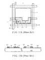
- FIG. 1Ais a plan view illustrating a pixel portion of a TFT-LCD.
- a signal line 40 and a scanning line 50vertically intersect each other as shown in FIG. 1A, wherein the scanning line 50 is directly connected to a gate electrode 14 of the pixel TFT portion and the signal line 40 is connected to a source electrode 11 S (as shown in FIG. 1B) at the pixel TFT.
- Storage capacitor electrodes 17 and 18are connected to a drain electrode 11 D of the pixel TFT.
- the upper electrode of the storage capacitoris connected to the outside of the pixel, that is, the contact region of the top capacitor electrode 18 is outside of the pixel.
- a pixel electrode 15is also connected to the drain electrode 11 D of the pixel TFT.
- FIGS. 1B to 1 Eare cross-sectional views including a series of fabrication processes for a pixel (taken along line a—a′ of FIG. 1A) and the drive circuit thereof.
- a pixeltaken along line a—a′ of FIG. 1A
- an n-type heavily doped silicon layer and a metal layerare sequentially formed on an insulating substrate 1000 .
- source and drain electrode regions 11 S and 11 D of the pixel TFTare defined wherein the drain region 11 D includes a first storage capacitor electrode 17 , and source and drain electrode regions 21 S and 21 D of the n-type TFT are also defined at the drive circuit.
- a silicon thin filmis subsequently formed on the overall surface over the substrate.
- the silicon thin filmis defined by a photolithography and an etching technique (a second photo mask) to form a predetermined region 10 ′ for a channel 10 and a lightly doped drain (LDD) 12 of the pixel TFT and another predetermined region 20 n ′ for a channel 20 n and a lightly doped drain (LDD) 22 of a n-type TFT, wherein the defined silicon regions 10 ′ and 20 n ′ are superposed on the corresponding source/drain regions thereof to form electrical connections.
- the silicon thin filmis also defined to form the other predetermined region 20 p ′ for a channel 20 p and source/drain electrodes 23 S, 23 D of a p-type TFT.
- an oxide layer and a gate metal layerare sequentially formed over the substrate.
- a gate electrode 14 , a storage capacitor dielectric layer 100 and a storage capacitor top electrode 18 of the pixel TFTare defined by a photolithographic and an etching technique (a third photo mask).
- a gate electrode 24 n of the n-type TFT and a gate electrode 24 p of the p-type TFTare defined.
- n-type impuritiesare lightly doped into the substrate including the pixel TFT and the n-type TFT and the p-type TFT at the drive circuit.
- a photoresist pattern 63is formed (a fourth photo mask) to cover the n-type TFT at the pixel and drive circuit portions and to bare the silicon thin film of the p-type TFT. Then, p-type conductive impurities are implanted to form source and drain electrodes 23 S and 23 D of the p-type TFT. Thereafter, the photoresist pattern 63 is removed. As shown in FIG. 1E, a passivation layer 300 is deposited on the overall surface over the substrate and then, contact holes are formed by a photolithography and an etching technique (a fifth photo mask) respectively at the pixel portion and the drive circuit portion.
- a pixel electrode 15is defined by a photolithography and etching technique (a sixth photo mask) and connected to the storage capacitor and the pixel TFT, and simultaneously, a transparent conductive line 25 is formed for connecting the p-type TFT and the nN-type TFT at the drive circuit.
- a method of forming a liquid crystal display device with a pixel TFT, a bottom electrode of pixel capacitor CL, and a storage capacitor Cs in a pixel region, and an n-type TFT and a p-type TFT in a driving circuit regionis disclosed. Firstly, a transparent conductive oxide layer, a metal layer and an n-type heavy doped silicon layer are sequentially formed on a glass substrate. Thereafter, a patterning step is performed to define some predefined regions for above devices.
- a first, a second, and a third preserved regionrespectively, for a LDD region of the n type TFT, source/drain regions for the p type TFT and a LDD region for pixel TFT and Cs.
- gate electrodesare formed for aforementioned TFT and an upper electrode for Cs.
- a blanket nLDD implantis performed by implant n-type impurities into the active layer.
- a p type source/drain implantis carried out using a photoresist pattern as a mask.
- a passivation layeris formed on all areas. Next an annealing is performed to active the implant impurities. Another patterning process is then performed to form contacts for driving circuit and end terminal of pixel panel by patterning the passivation layer and form the bottom electrode of C L by further patterning the n-type heavy doped silicon layer, and the metal layer to expose the transparent conductive oxide layer.
- FIG. 1Ais a top-view of one pixel of a TFT-LCD in accordance with the prior art.
- FIG. 1B to FIG. 1Fare a series of cross-sectional views of fabricating processes for a TFT-LCD in accordance with the prior art.
- FIG. 2Ais a top-view of one pixel of a TFT-LCD in accordance with the present invention.
- FIG. 2B to FIG. 2Gare a series of cross-sectional views of fabricating processes for a TFT-LCD in accordance with the present invention, wherein the portion of pixel is along line a-a′ of FIG. 2A.
- the present inventionis to use the least mask to fabricate the LCD device with driving circuit. Additional features and advantages of the invention will be set forth in the description which follows,
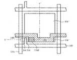
- FIG. 2Ashows a top view of a pixel element of a LCD panel according to the present invention.
- the scan line 140cross to and perpendicular to the signal line 124 s .
- the scan line 140connects the gate electrodes 140 i of the pixel TFTs arranged on one row.
- the signal line 124 sconnects the source electrodes of the pixel TFTs arranged on a column.
- the label 104indicates a transparent conductive layer, which is indium tin oxide layer(ITO).
- the label 140 cdenotes a stored capacitor, which is connected to the drain electrode 124 d by means of IT 0104 .
- FIG. 2B to FIG. 2Care cross-sectional views along a-a′ of FIG. 2A.
- a transparent conductive oxide layer 104 , a metal layer 105are sequentially formed on a transparent substrate, which is divided into drive circuit region 100 , and pixel region 101 .
- an n+ conductive impurity doped silicon layer 110is optionally deposited on the metal layer 105 .
- the transparent conductive oxide layer 104is an indium tin oxide layer (ITO) or a cadmium tin oxide layer.
- the n+ conductive impurity doped silicon layer 110can be either a polysilicon layer or an amorphous layer by in-situ doped.
- a lithographic and an etching processare successively performed to form a source electrode 120 s and a drain electrode 120 d of n-type TFT and a source electrode of p-type electrode 122 s on the drive circuit region 100 .
- a source electrode 124 s , a drain electrode 124 d , and a preserved region for pixel capacitor and for storage capacitorare also defined on the pixel region 101 .
- an un-doped amorphous layer 130 and gate oxide layer 135are then deposited in order on the entire areas. Thereafter, a LASER crystallizing process is conducted to transfer all amorphous silicon layers to polysilicon layers. After that the un-doped polysilicon layer 130 and gate oxide layer 135 are patterned so as to define preserved regions 125 , 126 , 127 , and 128 , for n-type TFT, p-type TFT, pixel TFT, and storage capacitor, respectively.
- the preserved region 125overlay a portion of the source electrode 120 s and the drain electrode 120 d .
- the preserved region 126overlay a portion of the source electrode 122 s and the drain electrode 120 d .
- the preserved region 127overlay a portion of the source electrode 124 s and the drain electrode 124 d.
- a metal layeris deposited on the entire areas.
- a patterning processis then carried out to form a gate electrode 140 i of the pixel TFT and a top electrode 140 c of the storage capacitor on the pixel region 101 as well as a reference electrode VSS and gate electrodes 140 n , 140 p of the n-type TFT and the p-type electrode, respectively, on the drive circuit region 100 .
- the remnant region of the preserved regions 125 on the left hand side and right hand side of the gate electrode 140 nare to preserve for forming LDD (lightly doped drain) regions 142 .
- the remnant region of the preserved regions 127are to form LDD regions 144 .
- the remnant regions of the preserved regions 126are to form a source electrode and a drain electrode of p-type TFT.
- an nLDD ion implant using n-type conductive impuritiesis implemented by using all gate electrodes as masks.
- a first photoresist pattern 150 containing an opening 151is coated on all areas.
- the opening 151is to expose the preserved region 126 .
- a heavily doped process with p-type conductive impuritiesis then performed to form a source region 143 s and a drain region 143 d of the p-type TFT.
- a passivation layer 160is then coated on all surfaces.
- the passivation layer 160is to flat the surface.
- the passivation layer 160can be formed by a way selected from the following: (1) blanket forming a nitride layer;. (2) forming a nitride layer firstly and then depositing an oxide layer; (3) forming a nitride layer and then forming a photosensitive resin layer. (4) forming a photosensitive resin layer.
- an anneal processis required.
- the anneal processcan be done before or post the passivation layer formation.
- the anneal processis performed in hydrogen ambient, which can cure those silicon dangling bonds during processes.
- passivation layer made of photosensitive resinIn case of passivation layer made of photosensitive resin.
- the anneal processshould be carried out before the photosensitive resin layer formation.
- the passivation layer 160is patterned to form contacts (not shown) on the end terminal of the panel of the LCD as well as to expose the ITO on the pixel capacitor.
- the processcan be done by etching in terms of photoresist pattern layer 170 or a photosensitive resin pattern layer as a mask.
- the photosensitive resin layerneeds an uV illuminating process to improve the transparency.
Landscapes
- Physics & Mathematics (AREA)
- Nonlinear Science (AREA)
- Mathematical Physics (AREA)
- Chemical & Material Sciences (AREA)
- Crystallography & Structural Chemistry (AREA)
- General Physics & Mathematics (AREA)
- Optics & Photonics (AREA)
- Liquid Crystal (AREA)
- Thin Film Transistor (AREA)
Abstract
Description
- 1. Field of the Invention[0001]
- The present invention relates to a liquid crystal display (LCD) device, and more particularly to a polysilicon type LCD.[0002]
- 2. Description of the Prior Art[0003]
- A liquid crystal display (LCD) is a flat panel display with characteristic of low power consumption. In comparison with a cathode ray tube (CRT) display of the same viewing size, what the liquid crystal display provided is much lower in occupied space and weight and without a curved panel problem. Hence, the popular of the liquid crystal display prompts the relates products being widely applied in various sorts of merchandises such as pocket calculators, electronic dictionaries, watches, mobile phones, portable notebooks, communication terminal, display panels, desk-top monitors and even high dpi (dots per inch) televisions (HDTV) etc. Consequently, the popularity of display and correlated products thereof seems promote the LCD to become the most brilliant star in the present century. Among various LCD display type, the most attractive type is TFT(thin film transistor)-LCD. Due to large viewing angle and high contrast characteristics, the TFT-LCD display of active type are better than those of a super-twisted nematic liquid crystal display (STN-LCD) of passive matrix type. Moreover, the TFT-LCD shows more rapid response time (such as several ms) than the STN-LCD does (such as several hundred milliseconds).[0004]
- In a conventional LCD, an amorphous silicon (a—Si) has been a long term choice of material for a thin film transistor (TFT) to fabricate an LCD. However, a polysilicon substitute for the amorphous silicon for the TFT is become a trend due to the polysilicon has a higher carrier (electron or hole) mobility than the amorphous silicon. Additionally, the polysilicon TFT has extra benefits such as the driving circuit with complimentary metal-oxide-semiconductor (CMOS) TFT on the LCD panel can be formed simultaneously with the pixel fabrication. As a result of the above-mentioned, the switch performance of the polysilicon-type TFT-LCD is better than the amorphous-type silicon TFT-LCD.[0005]
- Certainly, the polysilicon TFT-LCD is not perfect. For instance, when the TFT is at the off-state, often there is still a large drain leakage current. However, it can usually be overcome by the technique of a lightly doped drain (LDD) or a dual gate structure. The U.S. Pat. No. 5,940,151 invented by Yong-Min Ha etc. is one example.[0006]
- The fabricating method of Ha's patent is briefly described as follows: Firstly, please refer to FIG. 1A, which is a plan view illustrating a pixel portion of a TFT-LCD. A[0007]
signal line 40 and ascanning line 50 vertically intersect each other as shown in FIG. 1A, wherein thescanning line 50 is directly connected to agate electrode 14 of the pixel TFT portion and thesignal line 40 is connected to asource electrode 11S (as shown in FIG. 1B) at the pixel TFT.Storage capacitor electrodes drain electrode 11D of the pixel TFT. The upper electrode of the storage capacitor is connected to the outside of the pixel, that is, the contact region of thetop capacitor electrode 18 is outside of the pixel. Apixel electrode 15 is also connected to thedrain electrode 11D of the pixel TFT. - FIGS. 1B to[0008]1E are cross-sectional views including a series of fabrication processes for a pixel (taken along line a—a′ of FIG. 1A) and the drive circuit thereof. First of all, an n-type heavily doped silicon layer and a metal layer are sequentially formed on an
insulating substrate 1000. Then, through a photolithography and an etching technique (a first photo mask), source anddrain electrode regions drain region 11D includes a firststorage capacitor electrode 17, and source anddrain electrode regions predetermined region 10′ for achannel 10 and a lightly doped drain (LDD)12 of the pixel TFT and anotherpredetermined region 20n′ for achannel 20nand a lightly doped drain (LDD)22 of a n-type TFT, wherein the definedsilicon regions 10′ and20n′ are superposed on the corresponding source/drain regions thereof to form electrical connections. Moreover, the silicon thin film is also defined to form the otherpredetermined region 20p′ for achannel 20pand source/drain electrodes - Referring to FIG. 1C, an oxide layer and a gate metal layer are sequentially formed over the substrate. Then, a[0009]
gate electrode 14, a storage capacitordielectric layer 100 and a storagecapacitor top electrode 18 of the pixel TFT are defined by a photolithographic and an etching technique (a third photo mask). Simultaneously, at the drive circuit portion, agate electrode 24nof the n-type TFT and agate electrode 24pof the p-type TFT are defined. Thereafter, n-type impurities are lightly doped into the substrate including the pixel TFT and the n-type TFT and the p-type TFT at the drive circuit. - Turning to the cross-sectional view shown in FIG. 1D, a[0010]
photoresist pattern 63 is formed (a fourth photo mask) to cover the n-type TFT at the pixel and drive circuit portions and to bare the silicon thin film of the p-type TFT. Then, p-type conductive impurities are implanted to form source anddrain electrodes photoresist pattern 63 is removed. As shown in FIG. 1E, apassivation layer 300 is deposited on the overall surface over the substrate and then, contact holes are formed by a photolithography and an etching technique (a fifth photo mask) respectively at the pixel portion and the drive circuit portion. Thereafter, an ITO is deposited on the overall surface over the substrate including thepassivation layer 300 and the contact holes. Finally, apixel electrode 15 is defined by a photolithography and etching technique (a sixth photo mask) and connected to the storage capacitor and the pixel TFT, and simultaneously, a transparent conductive line25 is formed for connecting the p-type TFT and the nN-type TFT at the drive circuit. - A method of forming a liquid crystal display device with a pixel TFT, a bottom electrode of pixel capacitor CL, and a storage capacitor Cs in a pixel region, and an n-type TFT and a p-type TFT in a driving circuit region is disclosed. Firstly, a transparent conductive oxide layer, a metal layer and an n-type heavy doped silicon layer are sequentially formed on a glass substrate. Thereafter, a patterning step is performed to define some predefined regions for above devices. After an un-doped active layer and a gate oxide layer are formed in order on all patterned surfaces, another patterning step is done to form a first, a second, and a third preserved region, respectively, for a LDD region of the n type TFT, source/drain regions for the p type TFT and a LDD region for pixel TFT and Cs. Afterward, gate electrodes are formed for aforementioned TFT and an upper electrode for Cs. Subsequently, a blanket nLDD implant is performed by implant n-type impurities into the active layer. Thereafter, a p type source/drain implant is carried out using a photoresist pattern as a mask. After removing the photoresist pattern, a passivation layer is formed on all areas. Next an annealing is performed to active the implant impurities. Another patterning process is then performed to form contacts for driving circuit and end terminal of pixel panel by patterning the passivation layer and form the bottom electrode of C[0011]Lby further patterning the n-type heavy doped silicon layer, and the metal layer to expose the transparent conductive oxide layer.
- The foregoing aspects and many of the attendant advantages of this invention will become more readily appreciated as the same becomes better understood by reference to the following detailed description, when taken in conjunction with the accompanying drawings, wherein:[0012]
- FIG. 1A is a top-view of one pixel of a TFT-LCD in accordance with the prior art.[0013]
- FIG. 1B to FIG. 1F are a series of cross-sectional views of fabricating processes for a TFT-LCD in accordance with the prior art.[0014]
- FIG. 2A is a top-view of one pixel of a TFT-LCD in accordance with the present invention.[0015]
- FIG. 2B to FIG. 2G are a series of cross-sectional views of fabricating processes for a TFT-LCD in accordance with the present invention, wherein the portion of pixel is along line a-a′ of FIG. 2A.[0016]
- The present invention is to use the least mask to fabricate the LCD device with driving circuit. Additional features and advantages of the invention will be set forth in the description which follows,[0017]
- Referring to FIG. 2A, shows a top view of a pixel element of a LCD panel according to the present invention. In figure, the[0018]
scan line 140 cross to and perpendicular to thesignal line 124s. Thescan line 140 connects thegate electrodes 140iof the pixel TFTs arranged on one row. Thesignal line 124sconnects the source electrodes of the pixel TFTs arranged on a column. Thelabel 104 indicates a transparent conductive layer, which is indium tin oxide layer(ITO). Thelabel 140cdenotes a stored capacitor, which is connected to thedrain electrode 124dby means of IT0104. - As to fabricating processes, please refer to following figures: FIG. 2B to FIG. 2C, which are cross-sectional views along a-a′ of FIG. 2A.[0019]
- Referring to FIG. 2B. a transparent[0020]
conductive oxide layer 104, ametal layer 105 are sequentially formed on a transparent substrate, which is divided intodrive circuit region 100, andpixel region 101. Afterward, an n+ conductive impurity dopedsilicon layer 110 is optionally deposited on themetal layer 105. The transparentconductive oxide layer 104 is an indium tin oxide layer (ITO) or a cadmium tin oxide layer. The n+ conductive impurity dopedsilicon layer 110 can be either a polysilicon layer or an amorphous layer by in-situ doped. Thereafter, a lithographic and an etching process are successively performed to form asource electrode 120sand adrain electrode 120dof n-type TFT and a source electrode of p-type electrode 122son thedrive circuit region 100. In addition, asource electrode 124s, adrain electrode 124d, and a preserved region for pixel capacitor and for storage capacitor are also defined on thepixel region 101. - Subsequently, referring to FIG. 2C, an un-doped[0021]
amorphous layer 130 andgate oxide layer 135 are then deposited in order on the entire areas. Thereafter, a LASER crystallizing process is conducted to transfer all amorphous silicon layers to polysilicon layers. After that theun-doped polysilicon layer 130 andgate oxide layer 135 are patterned so as to define preservedregions region 125 overlay a portion of thesource electrode 120sand thedrain electrode 120d. The preservedregion 126 overlay a portion of thesource electrode 122sand thedrain electrode 120d. The preservedregion 127 overlay a portion of thesource electrode 124sand thedrain electrode 124d. - Referring to FIG. 2D, a metal layer is deposited on the entire areas. A patterning process is then carried out to form a[0022]
gate electrode 140iof the pixel TFT and atop electrode 140cof the storage capacitor on thepixel region 101 as well as a reference electrode VSS andgate electrodes drive circuit region 100. - It is noted that the remnant region of the preserved[0023]
regions 125 on the left hand side and right hand side of thegate electrode 140nare to preserve for forming LDD (lightly doped drain)regions 142. The remnant region of the preservedregions 127 are to formLDD regions 144. The remnant regions of the preservedregions 126 are to form a source electrode and a drain electrode of p-type TFT. Thereafter, an nLDD ion implant using n-type conductive impurities is implemented by using all gate electrodes as masks. - Referring to FIG. 2E, a[0024]
first photoresist pattern 150 containing anopening 151 is coated on all areas. Theopening 151 is to expose the preservedregion 126. A heavily doped process with p-type conductive impurities is then performed to form asource region 143sand adrain region 143dof the p-type TFT. - Referring to FIG. 2F, after stripping the[0025]
photoresist 150, apassivation layer 160 is then coated on all surfaces. Thepassivation layer 160 is to flat the surface. Thepassivation layer 160 can be formed by a way selected from the following: (1) blanket forming a nitride layer;. (2) forming a nitride layer firstly and then depositing an oxide layer; (3) forming a nitride layer and then forming a photosensitive resin layer. (4) forming a photosensitive resin layer. - To active the doped impurities, an anneal process is required. The anneal process can be done before or post the passivation layer formation. Preferably, the anneal process is performed in hydrogen ambient, which can cure those silicon dangling bonds during processes. In case of passivation layer made of photosensitive resin. The anneal process should be carried out before the photosensitive resin layer formation.[0026]
- Referring to FIG. 2G, the[0027]
passivation layer 160 is patterned to form contacts (not shown) on the end terminal of the panel of the LCD as well as to expose the ITO on the pixel capacitor. The process can be done by etching in terms ofphotoresist pattern layer 170 or a photosensitive resin pattern layer as a mask. The photosensitive resin layer needs an uV illuminating process to improve the transparency. - As is understood by a person skilled in the art, the foregoing preferred embodiments of the present invention are illustrated of the present invention rather than limiting of the present invention. It is intended to cover various modifications and similar arrangements included within the spirit and scope of the appended claims, the scope of which should be accorded the broadest interpretation so as to encompass all such modifications and similar structure[0028]
Claims (12)
Applications Claiming Priority (3)
| Application Number | Priority Date | Filing Date | Title |
|---|---|---|---|
| TW91120095A | 2002-09-03 | ||
| TW091120095ATWI234030B (en) | 2002-09-03 | 2002-09-03 | Liquid crystal display device integrated with driving circuit and method for fabrication the same |
| TW91120095 | 2002-09-03 |
Publications (2)
| Publication Number | Publication Date |
|---|---|
| US20040041954A1true US20040041954A1 (en) | 2004-03-04 |
| US6787405B2 US6787405B2 (en) | 2004-09-07 |
Family
ID=31974927
Family Applications (1)
| Application Number | Title | Priority Date | Filing Date |
|---|---|---|---|
| US10/413,309Expired - LifetimeUS6787405B2 (en) | 2002-09-03 | 2003-04-15 | Method of fabricating liquid crystal display devices integrated with driving circuit |
Country Status (2)
| Country | Link |
|---|---|
| US (1) | US6787405B2 (en) |
| TW (1) | TWI234030B (en) |
Cited By (2)
| Publication number | Priority date | Publication date | Assignee | Title |
|---|---|---|---|---|
| WO2020093442A1 (en)* | 2018-11-07 | 2020-05-14 | 深圳市华星光电半导体显示技术有限公司 | Method for manufacturing array substrate, and array substrate |
| CN115132762A (en)* | 2022-07-06 | 2022-09-30 | Tcl华星光电技术有限公司 | Array substrate, manufacturing method thereof, display panel and display device |
Families Citing this family (25)
| Publication number | Priority date | Publication date | Assignee | Title |
|---|---|---|---|---|
| US20090111206A1 (en) | 1999-03-30 | 2009-04-30 | Daniel Luch | Collector grid, electrode structures and interrconnect structures for photovoltaic arrays and methods of manufacture |
| US8076568B2 (en) | 2006-04-13 | 2011-12-13 | Daniel Luch | Collector grid and interconnect structures for photovoltaic arrays and modules |
| US8222513B2 (en) | 2006-04-13 | 2012-07-17 | Daniel Luch | Collector grid, electrode structures and interconnect structures for photovoltaic arrays and methods of manufacture |
| US8138413B2 (en) | 2006-04-13 | 2012-03-20 | Daniel Luch | Collector grid and interconnect structures for photovoltaic arrays and modules |
| US7507903B2 (en) | 1999-03-30 | 2009-03-24 | Daniel Luch | Substrate and collector grid structures for integrated series connected photovoltaic arrays and process of manufacture of such arrays |
| US8664030B2 (en) | 1999-03-30 | 2014-03-04 | Daniel Luch | Collector grid and interconnect structures for photovoltaic arrays and modules |
| US7898053B2 (en) | 2000-02-04 | 2011-03-01 | Daniel Luch | Substrate structures for integrated series connected photovoltaic arrays and process of manufacture of such arrays |
| US8198696B2 (en) | 2000-02-04 | 2012-06-12 | Daniel Luch | Substrate structures for integrated series connected photovoltaic arrays and process of manufacture of such arrays |
| US7898054B2 (en) | 2000-02-04 | 2011-03-01 | Daniel Luch | Substrate structures for integrated series connected photovoltaic arrays and process of manufacture of such arrays |
| US7157295B2 (en) | 2004-05-11 | 2007-01-02 | Tpo Displays Corporation | Method of manufacturing liquid crystal display |
| US7276724B2 (en)* | 2005-01-20 | 2007-10-02 | Nanosolar, Inc. | Series interconnected optoelectronic device module assembly |
| US7838868B2 (en) | 2005-01-20 | 2010-11-23 | Nanosolar, Inc. | Optoelectronic architecture having compound conducting substrate |
| US7732229B2 (en) | 2004-09-18 | 2010-06-08 | Nanosolar, Inc. | Formation of solar cells with conductive barrier layers and foil substrates |
| US8927315B1 (en) | 2005-01-20 | 2015-01-06 | Aeris Capital Sustainable Ip Ltd. | High-throughput assembly of series interconnected solar cells |
| KR100647695B1 (en)* | 2005-05-27 | 2006-11-23 | 삼성에스디아이 주식회사 | Organic thin film transistor, manufacturing method thereof and flat panel display device having same |
| US8729385B2 (en) | 2006-04-13 | 2014-05-20 | Daniel Luch | Collector grid and interconnect structures for photovoltaic arrays and modules |
| US9865758B2 (en) | 2006-04-13 | 2018-01-09 | Daniel Luch | Collector grid and interconnect structures for photovoltaic arrays and modules |
| US9006563B2 (en) | 2006-04-13 | 2015-04-14 | Solannex, Inc. | Collector grid and interconnect structures for photovoltaic arrays and modules |
| US8822810B2 (en) | 2006-04-13 | 2014-09-02 | Daniel Luch | Collector grid and interconnect structures for photovoltaic arrays and modules |
| US8884155B2 (en) | 2006-04-13 | 2014-11-11 | Daniel Luch | Collector grid and interconnect structures for photovoltaic arrays and modules |
| US9236512B2 (en) | 2006-04-13 | 2016-01-12 | Daniel Luch | Collector grid and interconnect structures for photovoltaic arrays and modules |
| US7670886B2 (en)* | 2006-06-22 | 2010-03-02 | Tpo Displays Corp. | Method for fabricating polysilicon film |
| US8247243B2 (en) | 2009-05-22 | 2012-08-21 | Nanosolar, Inc. | Solar cell interconnection |
| CN103151359B (en)* | 2013-03-14 | 2015-11-11 | 京东方科技集团股份有限公司 | A kind of display unit, array base palte and preparation method thereof |
| CN104078424B (en)* | 2014-06-30 | 2017-02-15 | 京东方科技集团股份有限公司 | Low-temperature poly-silicon TFT array substrate, manufacturing method thereof and display device |
Citations (5)
| Publication number | Priority date | Publication date | Assignee | Title |
|---|---|---|---|---|
| US5633182A (en)* | 1991-12-02 | 1997-05-27 | Canon Kabushiki Kaisha | Method of manufacturing an image display device with reduced cell gap variation |
| US5940151A (en)* | 1996-08-26 | 1999-08-17 | Lg Electronics, Inc. | Liquid crystal display and method for fabricating the same |
| US6278131B1 (en)* | 1999-01-11 | 2001-08-21 | Semiconductor Energy Laboratory Co., Ltd. | Pixel TFT and driver TFT having different gate insulation width |
| US6306694B1 (en)* | 1999-03-12 | 2001-10-23 | Semiconductor Energy Laboratory Co., Ltd. | Process of fabricating a semiconductor device |
| US6635521B2 (en)* | 1998-12-28 | 2003-10-21 | Fujitsu Display Technologies Corporation | CMOS-type semiconductor device and method of fabricating the same |
- 2002
- 2002-09-03TWTW091120095Apatent/TWI234030B/ennot_activeIP Right Cessation
- 2003
- 2003-04-15USUS10/413,309patent/US6787405B2/ennot_activeExpired - Lifetime
Patent Citations (5)
| Publication number | Priority date | Publication date | Assignee | Title |
|---|---|---|---|---|
| US5633182A (en)* | 1991-12-02 | 1997-05-27 | Canon Kabushiki Kaisha | Method of manufacturing an image display device with reduced cell gap variation |
| US5940151A (en)* | 1996-08-26 | 1999-08-17 | Lg Electronics, Inc. | Liquid crystal display and method for fabricating the same |
| US6635521B2 (en)* | 1998-12-28 | 2003-10-21 | Fujitsu Display Technologies Corporation | CMOS-type semiconductor device and method of fabricating the same |
| US6278131B1 (en)* | 1999-01-11 | 2001-08-21 | Semiconductor Energy Laboratory Co., Ltd. | Pixel TFT and driver TFT having different gate insulation width |
| US6306694B1 (en)* | 1999-03-12 | 2001-10-23 | Semiconductor Energy Laboratory Co., Ltd. | Process of fabricating a semiconductor device |
Cited By (2)
| Publication number | Priority date | Publication date | Assignee | Title |
|---|---|---|---|---|
| WO2020093442A1 (en)* | 2018-11-07 | 2020-05-14 | 深圳市华星光电半导体显示技术有限公司 | Method for manufacturing array substrate, and array substrate |
| CN115132762A (en)* | 2022-07-06 | 2022-09-30 | Tcl华星光电技术有限公司 | Array substrate, manufacturing method thereof, display panel and display device |
Also Published As
| Publication number | Publication date |
|---|---|
| TWI234030B (en) | 2005-06-11 |
| US6787405B2 (en) | 2004-09-07 |
Similar Documents
| Publication | Publication Date | Title |
|---|---|---|
| US6787405B2 (en) | Method of fabricating liquid crystal display devices integrated with driving circuit | |
| US7479657B2 (en) | Semiconductor device including active matrix circuit | |
| US6451630B2 (en) | Method for manufacturing a thin-film transistor | |
| US7335540B2 (en) | Low temperature polysilicon thin film transistor and method of manufacturing the same | |
| US7319243B2 (en) | Flat panel display device and method of manufacturing the same | |
| US6927464B2 (en) | Flat panel display device | |
| US7723734B2 (en) | LTPS-LCD structure and method for manufacturing the same | |
| US7755708B2 (en) | Pixel structure for flat panel display | |
| US20100133541A1 (en) | Thin film transistor array substrate, its manufacturing method, and liquid crystal display device | |
| US7973317B2 (en) | Array substrate for liquid crystal display and method for fabricating the same | |
| KR100268007B1 (en) | Fabrication method of lcd | |
| US7256457B2 (en) | Thin-film transistor device, utilizing different types of thin film transistors | |
| US6847414B2 (en) | Manufacturing method for liquid crystal display | |
| US20020149054A1 (en) | Flat panel display device and method of manufacturing the same | |
| US20060061701A1 (en) | Pixel of a liquid crystal panel, method of fabricating the same and driving method thereof | |
| US6534350B2 (en) | Method for fabricating a low temperature polysilicon thin film transistor incorporating channel passivation step | |
| US6703266B1 (en) | Method for fabricating thin film transistor array and driving circuit | |
| US20020168789A1 (en) | Method to fabricate flat panel display | |
| US7115431B2 (en) | Method of fabricating reflective liquid crystal display integrated with driving circuit | |
| US6670224B2 (en) | Method for manufacturing thin film transistors | |
| US6482685B1 (en) | Method for fabricating a low temperature polysilicon thin film transistor incorporating multi-layer channel passivation step | |
| CN1530718A (en) | Method for manufacturing reflective liquid crystal display and peripheral circuit | |
| KR100212270B1 (en) | Thin film transistor and manufacture thereof | |
| US7064017B2 (en) | Method of forming a CMOS transistor |
Legal Events
| Date | Code | Title | Description |
|---|---|---|---|
| AS | Assignment | Owner name:TOPPOLY OPTOELECTRONICS CORP., TAIWAN Free format text:ASSIGNMENT OF ASSIGNORS INTEREST;ASSIGNOR:CHEN, HSIN-MING;REEL/FRAME:013948/0492 Effective date:20030402 | |
| STCF | Information on status: patent grant | Free format text:PATENTED CASE | |
| AS | Assignment | Owner name:TPO DISPLAYS CORP., TAIWAN Free format text:CHANGE OF NAME;ASSIGNOR:TOPPOLY OPTOELECTRONICS CORPORATION;REEL/FRAME:019992/0734 Effective date:20060605 Owner name:TPO DISPLAYS CORP.,TAIWAN Free format text:CHANGE OF NAME;ASSIGNOR:TOPPOLY OPTOELECTRONICS CORPORATION;REEL/FRAME:019992/0734 Effective date:20060605 | |
| FPAY | Fee payment | Year of fee payment:4 | |
| AS | Assignment | Owner name:CHIMEI INNOLUX CORPORATION, TAIWAN Free format text:MERGER;ASSIGNOR:TPO DISPLAYS CORP.;REEL/FRAME:025749/0554 Effective date:20100318 | |
| FPAY | Fee payment | Year of fee payment:8 | |
| AS | Assignment | Owner name:INNOLUX CORPORATION, TAIWAN Free format text:CHANGE OF NAME;ASSIGNOR:CHIMEI INNOLUX CORPORATION;REEL/FRAME:032604/0487 Effective date:20121219 | |
| FPAY | Fee payment | Year of fee payment:12 |