US20040041927A1 - High intrascene dynamic range NTSC and PAL imager - Google Patents
High intrascene dynamic range NTSC and PAL imagerDownload PDFInfo
- Publication number
- US20040041927A1 US20040041927A1US10/230,205US23020502AUS2004041927A1US 20040041927 A1US20040041927 A1US 20040041927A1US 23020502 AUS23020502 AUS 23020502AUS 2004041927 A1US2004041927 A1US 2004041927A1
- Authority
- US
- United States
- Prior art keywords
- pixel
- signal
- row
- sampling
- circuit
- Prior art date
- Legal status (The legal status is an assumption and is not a legal conclusion. Google has not performed a legal analysis and makes no representation as to the accuracy of the status listed.)
- Granted
Links
Images


Classifications
- H—ELECTRICITY
- H04—ELECTRIC COMMUNICATION TECHNIQUE
- H04N—PICTORIAL COMMUNICATION, e.g. TELEVISION
- H04N23/00—Cameras or camera modules comprising electronic image sensors; Control thereof
- H04N23/70—Circuitry for compensating brightness variation in the scene
- H—ELECTRICITY
- H04—ELECTRIC COMMUNICATION TECHNIQUE
- H04N—PICTORIAL COMMUNICATION, e.g. TELEVISION
- H04N23/00—Cameras or camera modules comprising electronic image sensors; Control thereof
- H04N23/70—Circuitry for compensating brightness variation in the scene
- H04N23/741—Circuitry for compensating brightness variation in the scene by increasing the dynamic range of the image compared to the dynamic range of the electronic image sensors
- H—ELECTRICITY
- H04—ELECTRIC COMMUNICATION TECHNIQUE
- H04N—PICTORIAL COMMUNICATION, e.g. TELEVISION
- H04N25/00—Circuitry of solid-state image sensors [SSIS]; Control thereof
- H04N25/50—Control of the SSIS exposure
- H04N25/57—Control of the dynamic range
- H04N25/58—Control of the dynamic range involving two or more exposures
- H04N25/581—Control of the dynamic range involving two or more exposures acquired simultaneously
- H04N25/583—Control of the dynamic range involving two or more exposures acquired simultaneously with different integration times
- H—ELECTRICITY
- H04—ELECTRIC COMMUNICATION TECHNIQUE
- H04N—PICTORIAL COMMUNICATION, e.g. TELEVISION
- H04N25/00—Circuitry of solid-state image sensors [SSIS]; Control thereof
- H04N25/60—Noise processing, e.g. detecting, correcting, reducing or removing noise
- H04N25/616—Noise processing, e.g. detecting, correcting, reducing or removing noise involving a correlated sampling function, e.g. correlated double sampling [CDS] or triple sampling
- H—ELECTRICITY
- H04—ELECTRIC COMMUNICATION TECHNIQUE
- H04N—PICTORIAL COMMUNICATION, e.g. TELEVISION
- H04N25/00—Circuitry of solid-state image sensors [SSIS]; Control thereof
- H04N25/70—SSIS architectures; Circuits associated therewith
- H04N25/76—Addressed sensors, e.g. MOS or CMOS sensors
- H04N25/78—Readout circuits for addressed sensors, e.g. output amplifiers or A/D converters
Definitions
- the present inventionrelates generally to improved semiconductor imaging devices, and in particular to a CMOS imaging device having a high intrascene dynamic range.
- a large dynamic rangeis desirable in applications for sensing low light signals and capturing images with large variations in illuminance or brightness.
- the dynamic range of an image sensorcan be defined as the ratio of the minimum illuminance the sensor detects under saturation to the illuminance the sensor detects at signal-to-noise ratio (SNR) equal to 1.
- SNRsignal-to-noise ratio
- the dynamic range of a scenecan also be expressed as the ratio of its highest illumination level to its lowest illumination level.
- Intrascene dynamic rangerefers to the range of incident signal that can be accommodated by a sensor in a single frame of imager data.
- scenes that generate high dynamic range incident signalsinclude an indoor room with outdoor window, outdoor mixed shadow and bright sunshine, night time scenes combining artificial lighting and shadows, and in automotive context, an auto entering or about to leave a tunnel or shadowed area on a bright day.
- CMOS pixelLinear approaches have also been used to increase dynamic range where the integration time is varied during a frame capture to generate several different integrated pixel signals.
- integration timerefers to the time period during which a capacitor or charge well accumulates a charge or discharges a voltage from a pre-charge level (from a reset voltage) as a result of exposure of a photosensor to incident light. The integrated signal is then read-out and sampled. If a CMOS pixel's stored charge rises or falls to a point where it cannot further increase or decrease during the integration period, then it is said that the CMOS pixel has reached its saturation point.
- Conventional implementations which vary integration time during frame capturehave require additional logic and memory structures to store data generated by reading out the pixel at different points in time and thus are less than optimal as a design choice.
- FIG. 1shows how changes in integration time affects the magnitude of light intensity which a CMOS sensor can absorb without reaching the saturation voltage 1 thereby avoiding loss of image data.
- the FIG. 1 exampledemonstrates the behavior of the output signal from a pixel with a long integration time 2 and a short integration time 3.
- a signal output Sis proportional to light intensity and integration time. With a constant light input I over an integration time T int , the signal output can be expressed as
- I Lmax 5is the minimum light intensity which causes the pixel to saturate with integration time T L .
- I Lmin 6is the light intensity when signal output equals read noise with integration time T L .
- I Smax 7is the minimum light intensity which causes the pixel to saturate with integration time T S .
- I Smin 8is the light intensity when signal output equals read noise with integration time T S .
- dynamic rangeis extended by the ratio of the long integration time to the short integration time. For example, if long integration time is 20 and short integration time is 4, then DR is be multiplied by a factor of 5.
- a multiple integration approachwas first used in CCD sensors to increase dynamic range.
- a similar approachwas used in CMOS active pixel sensors and in charge multiplication devices (CMD) and since its initial use, the multiple integration approach has become one of the most commonly used techniques in high dynamic range sensors.
- CCDcharge multiplication devices
- a conventional high dynamic range imageruses two sample and hold circuits: one is a linear sample and hold circuit for each column of the array and captures a linear signal related to a difference between the pixel image output signal and a reset output signal to which the pixel is reset at the beginning of the integration period.
- the otheris an extended dynamic range (XDR) sample and hold circuit for each column of the array which captures an XDR signal related to a difference between the pixel image output signal and an XDR reset level to which the pixel is reset at a predetermined time before the end of the integration period.
- XDRextended dynamic range
- a high intrascene dynamic range CMOS active pixel sensor using dual samplinghas been previously created but has a number of shortcomings.
- a second column signal processing chain circuit and associated sample and hold circuitmust be added to the upper part of the CMOS sensor.
- row nis first selected for read out and copied into a lower sample and hold circuit. Row n is reset in the process. Immediately after row n is read out, row n ⁇ is then selected and sampled into the upper sample and hold circuit. Row n ⁇ is also reset as a consequence of being copied. Both sample and hold circuits are then scanned to read out stored data. After the two sample and hold circuits are read out, the row address increases by one, and the whole process starts over again.
- the second readoutalways lags ⁇ rows behind the first read out. If integration time is defined for the pixels copied to the lower sample and hold circuit as T 1 int, while the integration time for pixels copied to the upper sample and hold circuit as T 2 int, the ratio of T 1 int T 2 int is (N ⁇ ): ⁇ .
- T 1 int/T 2 intthe ratio of T 1 int T 2 int is (N ⁇ ): ⁇ .
- the intrascene dynamic range capability of the sensoris extended by the factor T 1 int/T 2 int.
- a major disadvantage of the dual sampling approachis that outputting the signal for two integration periods requires an additional analog memory on chip to synchronize these outputs.
- Another shortcomingis that dual sampling has not been optimally implemented for use with Phase Alternating Line (PAL) and National Television Standards Committee (NTSC) standard compliant image sensors.
- PALPhase Alternating Line
- NTSCNational Television Standards Committee
- the NTSC standardis the one most commonly used for video standards in North America and Japan. Europe uses PAL and the French use SECAM video standards. Both PAL and NTSC are 4:3 horizontal-to-vertical picture aspect ratios. Most television video transmitters and receivers use interlaced scanning rather than the non-interlaced progressive scanning.
- the inventionprovides a new method and apparatus for NTSC and PAL image sensors.
- the rows of pixelsare scanned so that each scan takes an odd row signal sample and, in some cases, an adjacent even row signal sample when specified conditions are met.
- One sampled row of the two adjacent rowsintegrate an image with a first integration period while the other adjacent row integrates an image with a second integration period.
- a fusion of adjacent row pixel image samplesoccurs to generate image data for a row.
- a progressive scan of pixel rowsis accomplished starting one end of the pixel array and continues until all adjacent row sets are selectively sampled and processed.
- a variety of fusion schemesare possible for fusing the pixel signals from the adjacent rows.
- FIG. 1shows a dynamic range extension for linear sensors using two integration times
- FIG. 2shows a comparison between progressive and interlaced scan scheme
- FIG. 3shows row organization of an imager matrix coupled to a column-parallel signal chain
- FIG. 4shows a basic architecture of a high dynamic range CMOS image sensor
- FIG. 5shows integration behavior of a CMOS imager pixel with respect to voltage over time
- FIG. 6 ashows a circuit implementation of a column parallel analog readout circuitry for a Selection-Based Fusion Algorithm constructed in accordance with an exemplary embodiment of the invention
- FIG. 6 bshows timing of a column parallel analog readout circuitry for a Selection-Based Fusion Algorithm constructed in accordance with an exemplary embodiment of the invention
- FIG. 7 ashows a circuit implementation for a column parallel analog readout circuitry for an Average-Based Fusion Algorithm constructed in accordance with an exemplary embodiment of the invention
- FIG. 7 bshows timing for a circuit implementation for a column parallel analog readout circuitry for an Average-Based Fusion Algorithm constructed in accordance with an exemplary embodiment of the invention
- FIG. 8 ashows a circuit implementation for a column parallel analog readout circuitry for a Selection and Average-Based Fusion Algorithm constructed in accordance with an exemplary embodiment of the invention.
- FIG. 8 bshows timing for a for a column parallel analog readout circuitry for a Selection and Average-Based Fusion Algorithms constructed in accordance with an exemplary embodiment of the invention.
- NTSC or PAL image sensorsperform imaging in two field captures at two time periods.
- Performing NTSC or PAL compatible image capture using progressive scan style with dual samplingrequires another approach.
- samples with different integration timecan be taken from two adjacent odd and even rows to produce each field of an NTSC and PAL image sensor so that high intrascene dynamic range is achieved with minimized circuitry.
- a fusion algorithmcan then be used to produce progressive style output using image signals from adjacent rows of pixels where the pixels of odd and even rows have different integration times.
- integrationcan be performed within a pixel array 12 where odd rows (e.g., 16 , 18 , 20 ) of pixels and even rows (e.g., 17 , 19 , 21 ) of pixels have different integration periods.
- odd row pixelshave a longer integration period, T long , which commences first to provide a pixel signal Vsig Long and even row pixels have a short integration period T short to provide a pixel signal output Vsig Short .
- Two pixel samples from pixels in adjacent odd (e.g., 16 ) and even rows (e.g., 17 ) that are in the same columncan be used as inputs to a fusion algorithm circuit to begin to produce a portion of a field.
- Another adjacent two pixel samples from the same columncan be sampled and input into a fusion algorithm to produce another portion of a field.
- the process of progressive adjacent row scanning with long and short integration times for adjacent pixels within a columnis repeated until all of the rows in a pixel array are sampled, processed and output.
- Each pixel which is sampledprovides a sampled pixel signal Vrst and a sampled image signal Vsig to a column line sample and hold circuit which performs the fusion operations.
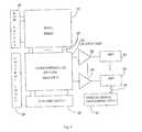
- FIG. 4shows one embodiment of an exemplary basic architecture of a high dynamic range CMOS image sensor with dual sampling of adjacent rows in a pixel array 12 .
- the exemplary sensorincludes a pixel array 12 coupled to a column-parallel analog readout circuitry 23 as well as row select 24 and column select circuits 25 .
- a plurality of circuits which implement the functions of a fusion algorithmare formed within the column-parallel analog readout 23 , each one coupled to a column line 22 in the pixel array 12 (inputs) and an output amplifier 29 (output).
- a control logic 27 unitcontrols column select unit 25 and row select unit 24 operations as well as operations within the column-parallel analog readout circuitry 23 .
- Each one of a plurality of on-chip analog to digital converters (ADC) 33are coupled to one of the plurality of output amplifiers 29 .
- a bus 36carries signals from the plurality of ADCs 33 to an on-chip digital image processing unit 37 .
- the digital image processing unitperforms on chip image processing such as color pixel processing.
- the control logic circuitry 27provides timing control of sensor components including switch operation within the circuit implementations of the fusion algorithms and pixel circuits.
- a variety of fusion algorithmscan be used for processing pixel data from adjacent rows with different integration time durations.
- Sampled pixel dataincludes Vsig Long and Vrst Long for the pixel having the long integration time and Vrst Short and Vsig Short for the pixels with the short integration time.
- Vsig Long and Vrst Longfor the pixel having the long integration time
- Vrst Short and Vsig Shortfor the pixels with the short integration time.
- An exemplary implementation for each exemplary algorithmwill be further explained below.
- a selection based fusion algorithm which compares a pixel signal Vsig Long with a thresholdis as follows:
- Data output in Algorithm 4is the digital output from the ADC.
- Pixel output in Algorithm 4is the difference between the initial state (Vrst) and the final state (Vsig) after a either a long or short integration in a pixel is concluded.
- the pixel output (Vrst ⁇ Vsig)is proportional to the integration time. The longer integration time, the larger the difference in a pixel output voltage from Vrst will be obtained up to the point of saturation voltage levels.
- ADC outputoccurs once for every two rows in an embodiment which incorporates an Algorithm 4.
- the threshold voltage compared to Vsigwill be
- . For example, given a power supply at 3.3 V and Vrst2V, Vsig can be below 1V.
- the threshold voltageoptimally can be set at 1V.
- threshold voltage settings and ADC 33 functioncan be obtained by use of the output amplifier 29 .
- a gain stageis between the analog column parallel circuit 23 and ADCs 33 .
- At gain2, even if
- a V threshold1.5
- V
- can be used with an operational amplifier to provide more flexibility in selecting threshold levels.
- Threshold voltage settingscan be changed freely in order to meet the requirements and design parameters of a given fusion algorithm design.
- a flag(explained below), can be set by a comparator and used to enable a subsequent sampling operation after comparison with the V threshold .
- Scomprises the fused Vsig value in the sampling capacitor for storing post-integration charge which is averaged then output to the ADC from the pixel capacitor.
- Data outputis the digital signal that is sent to an image processing unit for image processing.
- Pixel Output[( Vsig Long +Vsig Short )/2 ⁇ ( Vrst Long +Vrst Short )/2],
- Algorithm 6shows that averaging of pixel signals from a long integration row and short integration row will be done when Vsig Long is greater than threshold value Vthreshold, which represents pixel saturation voltage.
- Vthresholdrepresents pixel saturation voltage.
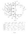
- FIGS. 3, 4, 6 a and timing diagram of FIG. 6 bA exemplary sample and hold circuit capable of executing an embodiment of a Selection-Based fusion Algorithm 4 implementation will now be explained with reference to circuits shown in FIGS. 3, 4, 6 a and timing diagram of FIG. 6 b .
- Each column line 22 in the pixel array 12is coupled to its own separate sample and hold/circuit which is shown in FIG. 6 a .
- a plurality of 6 a circuitsare formed within the column-parallel analog readout 23 .
- Each FIG. 6 a circuit outputis coupled to a one of a set of output amplifiers 29 shown in FIG. 4.
- FIG. 6 b timing diagramdoes not show relationships to integration time periods in the pixel array 12 rows. Integration is separately controlled by the timing generator in the control logic 27 circuitry (FIG. 4). Switch inputs, except Flag 73 , (FIG. 6 a ) are also controlled by the control logic circuit 27 .
- an odd row (e.g., 16 ) in the pixel array 12is selected by row select circuit 24 (FIG. 4).
- a flag 73 stored in latch 54is initially set to “1” or high.
- clamping switches ColClamp 75 , 76are closed which applies clamping voltage Vcl 57 to the backsides of sample and hold capacitors 55 (for Vsig), 65 (for Vrst).
- a Samp_Sig 66 signalcontrolled by control logic 27 and coupled to Samp_Sig switch 68 , is set high.
- the Samp_Sig switch 68is coupled between the column line 22 and a Vsig sampling capacitor 55 .
- Samp_Sig switch 68is responsive to an AND gate 50 .
- the AND gate 50opens or closes the Samp_Sig switch 68 based on Flag signal 73 and Samp_Sig 66 signal inputs.
- Samp_Sig switch 68is closed, a Vsig Long signal from a selected pixel coupled to column line 22 by a row select switch within the pixel (e.g., in row 16 ) is sampled and held in the Vsig sampling capacitor 55 .
- the Samp_Sig signal 66is set to “0” or low, which thereby opens switch 68 .
- a Samp_Rst 67 signalcontrolled by control logic 27 and coupled to Samp_Rst switch 63 , is set to “1” or high.
- the Samp_Rst switch 63is coupled between the column line 22 and a Vrst sampling capacitor 65 .
- Samp_Rst switch 63incorporates an AND gate 49 , which receives flag signal 73 and a Samp_Rst signal 67 .
- the Samp_Rst switch 63opens or closes the Samp_Rst switch 63 based on the Flag 73 and the Samp_Rst 67 signal inputs.
- the selected pixele.g., in row 16 ) is reset with reset voltage Vrst.
- Samp_Rst switch 63When Samp_Rst switch 63 is closed, a reset pixel signal in the selected pixel (e.g., in row 16 ) is sampled and held in the Vrst sampling capacitor 65 . Next, the Samp_Rst signal 67 is set low, which thereby opens switch 63 .
- Flag 73is either set high (“1”) or set low (“0”) when comparator 53 compares the sampled Vsig Long signal stored in capacitor 55 with V threshold 74 .
- Comparator 53has two inputs, one input being V threshold 74 and the other input coupled to the front (pixel array side) of the Vsig sample and hold capacitor 55 .
- V threshold 74is a value which is approximately equal to a saturation voltage for a pixel in pixel array 12 .
- the output of comparator 53generates a flag signal which is output to latch 54 .
- Latch 54stores and outputs Flag 73 .
- ColSel switch 64is coupled between the front (pixel array) side of sampling capacitors 55 , 65 and is controlled by control logic unit 27 .
- ColSel switch 69is coupled between the backside of sampling capacitor 55 and the Out_Neg 78 output to the opamp 29 .
- ColSel switch 70is coupled between the backside of sampling capacitor 65 and the Out_Pos 79 output to the opamp 29 .
- Comparator 53determines Vsig Long stored in sampling capacitor 55 is less than V threshold 74 , comparator sets latch 54 to maintain output a high (“1”) Flag 73 .
- capacitors 55 , 65are discharged (by a circuit not shown), row select 24 selects pixels of an adjacent even row (e.g., row 17 ), Vsig 51 and Vrst 61 of the even row pixel are sampled as described above, ColClamp switches 75 and 76 are opened, then capacitors 55 , 65 are then output into opamp 29 after the ColSel switches 64 , 70 , 69 are closed.
- row select 24selects the next odd row (e.g., row 18 ) and pixel processing recommences as described above on the next selected odd and adjacent even row (e.g., row 19 ). Processing of adjacent odd and even rows continues until all rows in the array have been sampled and processed.
- FIGS. 4, 7 a and 7 bAn exemplary sample and hold circuit capable of executing an embodiment of an Average-Based Fusion Algorithm 5 implementation will now be explained with reference to circuits shown in FIGS. 4, 7 a and 7 b .
- Each column line 22 in the pixel array 12is coupled to a separate FIG. 7 a sample and hold circuit.
- Each FIG. 7 a circuithas four inputs coupled to a single column line 22 , where each input is coupled, through a switch, to a sample and hold capacitor for storing a different pixel signal.
- One set of sample and hold capacitors 91 , 81store a Vsig 1 pixel signal (Vsig Long ) from an odd row (e.g., row 16 ) and a Vsig 2 pixel signal (Vsig Short ) from an adjacent an even row (e.g., row 17 ).
- Another set of sample and hold capacitors 83 , 93stores a respective Vrst 1 and Vrst 2 pixel reset signals from the selected odd (e.g., row 16 ) and even (e.g., row 17 ) rows.
- An averaging switch 95 , 96is coupled between each of the two sets of sample and hold capacitors 91 , 81 and 83 , 93 .
- the Vsig 1 and Visg 2 capacitorsare coupled to output Out_Neg line 111 and the Vrst 1 and Vrst 2 capacitors are coupled to output Out_Pos line 113 .
- Out_Neg 111 and Out_Pos 113 linesare respectively coupled to the negative and positive inputs of an opamp 29 .
- a plurality of FIG. 7 a circuitsare formed within the column-parallel analog readout 23 and each are coupled to a respective output amplifier 29 as shown in FIG. 4. Long and short integration is respectively accomplished in the odd and even rows of pixel array 12 before sample and hold processing. It should be noted that the switches in the FIG. 7 a circuit and the signals that drive the switches described in FIG. 7 b are referred to using the same identifiers and element numbers.
- an odd row(e.g., row 16 ) is selected by row select circuit 24 .
- sampling capacitors 91 , 81 , 83 and 93are clamped with clamping voltage Vcl 80 by closing ColCIamp switches 109 , 107 with the signal ColClamp.
- Samp_Sig 1 switch 103is closed by signal Samp_Sig 1 which permits a Vsig Long pixel signal to be sampled and held in Vsig 1 sampling capacitor 103 . Then Samp_Sig 1 switch 103 is opened.
- Control logicresets the selected odd row (e.g., row 16 ) with voltage Vrst 1 then, the Samp_Rst 1 switch 101 coupled between sampling capacitor 83 and column line input 22 is closed by a Samp_Rst 1 signal.
- Samp_Rst 1 switch 103When Samp_Rst 1 switch 103 is closed, the reset pixel signal Vrst 1 is sampled from the selected pixel (e.g., 16 ) and held in Vrst 1 sampling capacitor 83 , and then the SampRst 1 switch 101 is opened. Next, an adjacent even row (e.g., row 17 ) is selected.
- Samp_Sig 2 switch 105is closed by signal Samp_Sig 2 , Vsig Short pixel signal in the selected pixel is sampled and held in sampling capacitor 91 then Samp_Sig 2 switch 105 is opened.
- Samp_Rst 2 switch 99is closed by signal Samp_Rst 2 , the Vrst 2 86 signal in the selected pixel is sampled and held in sampling capacitor 93 and then Samp_Rst 2 switch 99 is opened.
- averagingis performed by closing an averaging switch 95 between capacitors 91 , 81 and another averaging switch 96 between capacitors 83 and 93 .
- clamping voltage Vcl 80is removed from capacitors 91 , 81 , 83 and 93 by opening Col_Clamp switches 107 and 109 with the ColCiamp signal.
- column select switches 100 , 97 and 98are closed by the ColSel signal which outputs the averaged Vsig and Vrst signals respectively stored in capacitors 91 , 81 and 83 , 93 to the opamp 29 through Out_Neg 111 and Out_Pos 113 lines.
- the circuitis next reset, then the next odd row (e.g., row 18 ) of pixel array 12 is selected and sampling of the selected odd row (e.g., row 18 ) as described above occurs.
- the even row adjacent to the previously selected odd rowis selected (e.g., row 19 ) and the two adjacent row averaging cycle commences as described above.
- the two-row average processing cyclecontinues until all rows have been sampled, averaged and output to output amplifier 29 .
- the integration cycle in the pixel array 12recommences as directed by control logic unit 27 .
- row processing cyclecommences again if so directed by control logic unit 27 .
- a exemplary sample and hold circuit capable of executing Combined Selection-Based and Average-Based Algorithm 6will now be explained with reference to circuits shown in FIGS. 3, 4, 8 a and 8 b . Integration is performed in the pixel array 12 so that odd rows (e.g., rows 16 , 18 , 20 ) of the pixel array 12 have a long integration time and even rows, (e.g., rows 17 , 19 , 21 ) of the pixel array 12 have a short integration time.
- odd rowse.g., rows 16 , 18 , 20
- even rowse.g., rows 17 , 19 , 21
- a column line 22 from the pixel array 12is coupled to four inputs of a sample and hold circuit.
- the first inputis a Vsig 1 input 133 which is coupled to a sampling capacitor 161 for storing and holding a Vsig Long pixel signal.
- the second input coupled to the array column line 22is the Vrst 1 signal input 151 which is coupled to a sampling capacitor 163 which stores and holds a Vrst 1 pixel reset signal.
- the third inputis a Vsig 2 input 129 which is coupled to a capacitor 137 which samples and holds a Vsig Short pixel signal.
- the fourth inputis a Vrst 2 input 155 which is coupled to a sampling capacitor 165 which samples and holds a Vrst 2 pixel reset signal.
- Averaging operationsare controlled by averaging switch 135 (on pixel side inputs and between capacitors 161 , 137 ) and average switch 159 (on pixel side inputs and between capacitors 163 , 165 ).
- Averaging switch 135is coupled to the front and between capacitors 137 and 161 .
- Comparator 121has as inputs a V threshold 119 input and is coupled to the pixel array 12 side of the Vsig 1 capacitor. Comparator 121 comparison signal is output to Latch 123 , which is a 1-bit memory element, that outputs Flag 125 to inverter 124 . Inverter 124 outputs Flag 126 signal to AND gates 134 , 136 . Average signal 135 , 159 is also coupled to AND gates 134 , 136 . AND gates 134 , 136 outputs are coupled respectively to averaging switches 135 , 159 . Capacitors 161 , 137 and 165 and 163 are respectively coupled to opamp 29 by outputs Out_Neg 143 and Out_Pos 173 .
- an odd row (e.g., row 16 ) in pixel array 12is selected by row select circuit 24 , then pixel signal Vsig Long is sampled at sampling capacitor 161 by operating Samp_Sig 1 switch 145 .
- each pixel in the selected rowis reset and the reset value (Vrst 1 ) 151 is sampled and held at sampling capacitor 163 by closing, then opening Samp_Rst 1 switch 149 .
- an adjacent even row (e.g., row 17 ) of the pixel array 12is selected by row select circuit 24 .
- Vsig Short pixel signal and pixel reset signal (Vrst 2 ) 155are respectively sampled and held in the second set of sampling capacitors 137 (Vsig 2 ), 165 (Vrst 2 ) using Samp_Sig 2 127 and Samp_Rst 2 157 switches.
- a comparator 121has one input coupled to the pixel array 12 side of capacitor 161 storing the sampled and held Vsig 1 133 signal and a second input coupled to a V threshold signal 119 .
- the comparator 121compares the Vsig 1 133 signal and the V theshold 119 signal to determine if Vsig 1 >V threshold . If Vsig 1 133 is greater than V threshold , then the comparator 121 sets latch 123 , which is a 1-bit memory storage unit low or “0”. Latch 123 outputs a Flag 125 value of “0” (Vsig 1 >Vthreshold) or “1” if (Vsig 1 ⁇ Vthreshold).
- Latch 123can be reset to store a “1” Flag 125 by control logic 27 in order to reset the Latch.
- Latch 123is coupled to an inverter 124 which outputs a Flag signal 126 (inverted Flag 125 ) which is in turn coupled to AND gates 134 , 136 .
- the AND gatesalso receive an average signal 131 from control logic unit 27 as well as the Flag 126 input signal.
- AND gates 134 , 136outputs respectively control averaging switches 135 , 159 .
- Averaging switch 135controls a line is coupled to the front or pixel array 12 side and between Vsig 1 and Vsig 2 capacitors 137 , 161 for performing charge averaging between the two capacitors.
- Averaging switch 159is coupled to the front or pixel array 12 side and between Vrst 1 and Vrs 2 capacitors 163 , 165 for performing charge averaging between the two capacitors.
- averagingwill occur between capacitor sets or averaging will be skipped depending on the Flag value 125 output by latch 123 .
- Charges stored on Vsig 1 capacitor 161 and Vsig 2 capacitor 137will be averaged in response to a Flag signal 126 .
- the charges stored in the Vrst 1 capacitor 163 and Vrst 2 capacitor 165will also simultaneously be averaged in response to a Flag signal.
- ColSel switch 147is coupled to the pixel array 12 side and between capacitor sets 161 , 137 and 165 , 163 .
- ColSel switch 171is coupled between opamp 29 and capacitors 163 , 165 .
- ColSel switch 141is coupled between opamp 29 and capacitors 137 , 161 .
- ColSel switches 147 , 141 and 171are closed so the two averaged signals on the two sets of capacitors storing Vsig 1 ( 161 ), Vsig 2 ( 137 ) and Vrst 1 ( 163 ), Vrst 2 ( 165 ) in the crowbar circuit become the differential input for operational amplifier (opamp) 29 (i.e., through Out_Neg 143 and Out_Pos 173 lines).
- the opamp 29 output voltageis analog to digital converted in ADC 33 .
- opamp 29outputs the averaged signals, then the next odd row is selected (e.g., row 18 ) and processed, along with adjacent even row (e.g., row 19 ). The sample and hold processing cycle described above is then repeated until each set of adjacent sets of odd and even rows in the pixel array 12 are processed.
- the pixel array 12can contain a variety of pixels which operate, for example, with rolling electronically controlled shutter operations or global pixels which contain extra storage elements to contain transferred pixel data for subsequent readout.
- a mechanical shuttercan also be used in conjunction with electronically controlled shutter operations in the pixel array 12 which is useful to control pixel integration.
- a gamma tablecan be used with the invention to compress the dynamic range of the fused high dynamic range image for displays which typically utilize 8-bit display devices. Range compression from, for example, a 12 bit input to an 8-bit output, is accomplished by using a Gamma table.
- the gamma tableprovides correction to a linear response or relationship which affects converted image data when an X-bit input is converted, or compressed, to a Y-bit output.
- the gamma table circuitcan be incorporated into the digital image processing unit 37 which can perform dynamic range compression associated with data conversion or compression.
- Another embodiment of the inventioncan include a circuit in the digital image processing unit 37 (FIG. 4) which receives the flag value stored in the latch (e.g., FIG. 6 a , 54 ) from an embodiment of a selection algorithm based implementation such as disclosed in the FIG. 6 a or FIG. 8 a circuits. Additional signal processing of a pixel signal can be performed in an imager processing unit 37 based upon the Flag value in a circuit implementation using a form of the selection-based fusion algorithm. Accordingly, the digital image processing unit 37 would receive not only the ADC(s) output, but also a flag value which is then used to perform further advanced image processing.
- control of the switches within the fusion algorithm sample and hold circuitscan also be controlled by other circuit(s) outside of the control logic unit 27 .
- control logiccan be included within the column select 25 circuitry or within the column parallel analog readout circuitry 23 .
Landscapes
- Engineering & Computer Science (AREA)
- Multimedia (AREA)
- Signal Processing (AREA)
- Transforming Light Signals Into Electric Signals (AREA)
Abstract
Description
- The present invention relates generally to improved semiconductor imaging devices, and in particular to a CMOS imaging device having a high intrascene dynamic range.[0001]
- An important performance characteristic of imaging devices is dynamic range. A large dynamic range is desirable in applications for sensing low light signals and capturing images with large variations in illuminance or brightness.[0002]
- In particular, the dynamic range of an image sensor can be defined as the ratio of the minimum illuminance the sensor detects under saturation to the illuminance the sensor detects at signal-to-noise ratio (SNR) equal to 1. The dynamic range of a scene can also be expressed as the ratio of its highest illumination level to its lowest illumination level.[0003]
- Intrascene dynamic range refers to the range of incident signal that can be accommodated by a sensor in a single frame of imager data. Examples of scenes that generate high dynamic range incident signals include an indoor room with outdoor window, outdoor mixed shadow and bright sunshine, night time scenes combining artificial lighting and shadows, and in automotive context, an auto entering or about to leave a tunnel or shadowed area on a bright day.[0004]
- Many different types of approaches for creating devices with high dynamic range have been described in the literature. A common denominator of most approaches rely on performing companding within the pixel by a having either a total conversion to a log scale (so-called logarithmic pixel) or a mixed linear and logarithmic response region in the pixel. These approaches have several major drawbacks. First, the knee point in linear-to-log transition is difficult to control leading to fixed pattern noise in the output image. Second, under low light the log portion of the circuit is slow to respond leading to lag. Third, a logarithmic representation of the signal in the voltage domain (or charge domain) means that small variations in signal due to fixed pattern noise leads to large variations in represented signal.[0005]
- Linear approaches have also been used to increase dynamic range where the integration time is varied during a frame capture to generate several different integrated pixel signals. In the context of a CMOS pixel, integration time refers to the time period during which a capacitor or charge well accumulates a charge or discharges a voltage from a pre-charge level (from a reset voltage) as a result of exposure of a photosensor to incident light. The integrated signal is then read-out and sampled. If a CMOS pixel's stored charge rises or falls to a point where it cannot further increase or decrease during the integration period, then it is said that the CMOS pixel has reached its saturation point. Conventional implementations which vary integration time during frame capture have require additional logic and memory structures to store data generated by reading out the pixel at different points in time and thus are less than optimal as a design choice.[0006]
- FIG. 1 shows how changes in integration time affects the magnitude of light intensity which a CMOS sensor can absorb without reaching the[0007]
saturation voltage 1 thereby avoiding loss of image data. In particular, the FIG. 1 example demonstrates the behavior of the output signal from a pixel with along integration time 2 and ashort integration time 3. - Capturing still images with different integration times and then merging them is an effective way to extend the dynamic range of a linear sensor without losing contrast at high light level, in a manner similar to how nonlinear sensors perform. For a linear sensor, a signal output S is proportional to light intensity and integration time. With a constant light input I over an integration time T[0008]int, the signal output can be expressed as
- S=ks·I·Tint (1)
- where k[0009]sis the pixel's sensitivity.
- where[0011]
I Lmax5 is the minimum light intensity which causes the pixel to saturate with integration time TL. ILmin6 is the light intensity when signal output equals read noise with integration time TL. ISmax7 is the minimum light intensity which causes the pixel to saturate with integration time TS. ISmin8 is the light intensity when signal output equals read noise with integration time TS. With two integration times (i.e., range 9), the extended dynamic range DRextcan be expressed as
- Accordingly, dynamic range (DR) is extended by the ratio of the long integration time to the short integration time. For example, if long integration time is 20 and short integration time is 4, then DR is be multiplied by a factor of 5.[0012]
- A multiple integration approach was first used in CCD sensors to increase dynamic range. A similar approach was used in CMOS active pixel sensors and in charge multiplication devices (CMD) and since its initial use, the multiple integration approach has become one of the most commonly used techniques in high dynamic range sensors.[0013]
- A conventional high dynamic range imager uses two sample and hold circuits: one is a linear sample and hold circuit for each column of the array and captures a linear signal related to a difference between the pixel image output signal and a reset output signal to which the pixel is reset at the beginning of the integration period. The other is an extended dynamic range (XDR) sample and hold circuit for each column of the array which captures an XDR signal related to a difference between the pixel image output signal and an XDR reset level to which the pixel is reset at a predetermined time before the end of the integration period.[0014]
- A high intrascene dynamic range CMOS active pixel sensor using dual sampling has been previously created but has a number of shortcomings. For example, a second column signal processing chain circuit and associated sample and hold circuit must be added to the upper part of the CMOS sensor. During operation, row n is first selected for read out and copied into a lower sample and hold circuit. Row n is reset in the process. Immediately after row n is read out, row n−Δ is then selected and sampled into the upper sample and hold circuit. Row n−Δ is also reset as a consequence of being copied. Both sample and hold circuits are then scanned to read out stored data. After the two sample and hold circuits are read out, the row address increases by one, and the whole process starts over again. In this readout scheme, the second readout always lags Δ rows behind the first read out. If integration time is defined for the pixels copied to the lower sample and hold circuit as T[0015]1int, while the integration time for pixels copied to the upper sample and hold circuit as T2int, the ratio of T1int T2int is (N−Δ):Δ. The intrascene dynamic range capability of the sensor is extended by the factor T1int/T2int.
- There are several advantages of the dual sampling approach. First, linearity of the signal is preserved. Second, no modification to the standard CMOS APS pixel is required to achieve high dynamic range so that fill factor and pixel size can be optimized. Third, the low read noise of the CMOS APS pixel is preserved. Fourth, the extended dynamic range operation can be optionally employed, depending on control signals to the chip, without sacrificing sensor performance.[0016]
- A major disadvantage of the dual sampling approach is that outputting the signal for two integration periods requires an additional analog memory on chip to synchronize these outputs. Another shortcoming is that dual sampling has not been optimally implemented for use with Phase Alternating Line (PAL) and National Television Standards Committee (NTSC) standard compliant image sensors.[0017]
- The NTSC standard is the one most commonly used for video standards in North America and Japan. Europe uses PAL and the French use SECAM video standards. Both PAL and NTSC are 4:3 horizontal-to-vertical picture aspect ratios. Most television video transmitters and receivers use interlaced scanning rather than the non-interlaced progressive scanning.[0018]
- Conventional dual sample image sensors using the NTSC and PAL format produce interlaced output, not progressive scan-output (non-interlaced). As shown in FIG. 2, an[0019]
image frame 15 containing rows and columns of pixels is divided into two fields: an odd field (Field1)13 consisting of all the odd numbered rows of pixels, and the even field (Field2)14 consisting of all the even numbered rows of pixels. The two fields per frame scheme is known as a 2:1 interlace. Half of the frame is recorded by the odd field at time T1, and the other half of the frame is recorded by the even field at time T2. Progressive scan sensors read out a complete frame with no interlacing one row at a time. Progressive scan methods have desirable attributes such as better image capture for subjects which are moving. Thus, it would be desirable to have an increased dynamic image CMOS image sensor which is NTSC and PAL compliant and which provides a progressive scan output. - The invention provides a new method and apparatus for NTSC and PAL image sensors. The rows of pixels are scanned so that each scan takes an odd row signal sample and, in some cases, an adjacent even row signal sample when specified conditions are met. One sampled row of the two adjacent rows integrate an image with a first integration period while the other adjacent row integrates an image with a second integration period. A fusion of adjacent row pixel image samples occurs to generate image data for a row. A progressive scan of pixel rows is accomplished starting one end of the pixel array and continues until all adjacent row sets are selectively sampled and processed. A variety of fusion schemes are possible for fusing the pixel signals from the adjacent rows.[0020]
- The above and other features and advantages of the invention will be more readily understood from the following detailed description of the invention which is provided in connection with the accompanying drawings.[0021]
- FIG. 1 shows a dynamic range extension for linear sensors using two integration times;[0022]
- FIG. 2 shows a comparison between progressive and interlaced scan scheme;[0023]
- FIG. 3 shows row organization of an imager matrix coupled to a column-parallel signal chain;[0024]
- FIG. 4 shows a basic architecture of a high dynamic range CMOS image sensor;[0025]
- FIG. 5 shows integration behavior of a CMOS imager pixel with respect to voltage over time;[0026]
- FIG. 6[0027]ashows a circuit implementation of a column parallel analog readout circuitry for a Selection-Based Fusion Algorithm constructed in accordance with an exemplary embodiment of the invention;
- FIG. 6[0028]bshows timing of a column parallel analog readout circuitry for a Selection-Based Fusion Algorithm constructed in accordance with an exemplary embodiment of the invention;
- FIG. 7[0029]ashows a circuit implementation for a column parallel analog readout circuitry for an Average-Based Fusion Algorithm constructed in accordance with an exemplary embodiment of the invention;
- FIG. 7[0030]bshows timing for a circuit implementation for a column parallel analog readout circuitry for an Average-Based Fusion Algorithm constructed in accordance with an exemplary embodiment of the invention;
- FIG. 8[0031]ashows a circuit implementation for a column parallel analog readout circuitry for a Selection and Average-Based Fusion Algorithm constructed in accordance with an exemplary embodiment of the invention; and
- FIG. 8[0032]bshows timing for a for a column parallel analog readout circuitry for a Selection and Average-Based Fusion Algorithms constructed in accordance with an exemplary embodiment of the invention.
- Conventional interlaced NTSC or PAL image sensors perform imaging in two field captures at two time periods. Performing NTSC or PAL compatible image capture using progressive scan style with dual sampling requires another approach. For example, referring to FIG. 3, samples with different integration time can be taken from two adjacent odd and even rows to produce each field of an NTSC and PAL image sensor so that high intrascene dynamic range is achieved with minimized circuitry. A fusion algorithm can then be used to produce progressive style output using image signals from adjacent rows of pixels where the pixels of odd and even rows have different integration times.[0033]
- Referring to FIG. 3, integration can be performed within a[0034]
pixel array 12 where odd rows (e.g.,16,18,20) of pixels and even rows (e.g.,17,19,21) of pixels have different integration periods. In an exemplary embodiment, odd row pixels have a longer integration period, Tlong, which commences first to provide a pixel signal VsigLongand even row pixels have a short integration period Tshortto provide a pixel signal output VsigShort. Two pixel samples from pixels in adjacent odd (e.g.,16) and even rows (e.g.,17) that are in the same column can be used as inputs to a fusion algorithm circuit to begin to produce a portion of a field. Next, another adjacent two pixel samples from the same column can be sampled and input into a fusion algorithm to produce another portion of a field. The process of progressive adjacent row scanning with long and short integration times for adjacent pixels within a column is repeated until all of the rows in a pixel array are sampled, processed and output. Each pixel which is sampled provides a sampled pixel signal Vrst and a sampled image signal Vsig to a column line sample and hold circuit which performs the fusion operations. - FIG. 4 shows one embodiment of an exemplary basic architecture of a high dynamic range CMOS image sensor with dual sampling of adjacent rows in a[0035]
pixel array 12. The exemplary sensor includes apixel array 12 coupled to a column-parallelanalog readout circuitry 23 as well as row select24 and columnselect circuits 25. A plurality of circuits which implement the functions of a fusion algorithm (described below) are formed within the column-parallel analog readout 23, each one coupled to acolumn line 22 in the pixel array12 (inputs) and an output amplifier29 (output). Acontrol logic 27 unit controls columnselect unit 25 and rowselect unit 24 operations as well as operations within the column-parallelanalog readout circuitry 23. Each one of a plurality of on-chip analog to digital converters (ADC)33 are coupled to one of the plurality ofoutput amplifiers 29. Abus 36 carries signals from the plurality ofADCs 33 to an on-chip digitalimage processing unit 37. The digital image processing unit performs on chip image processing such as color pixel processing. Thecontrol logic circuitry 27 provides timing control of sensor components including switch operation within the circuit implementations of the fusion algorithms and pixel circuits. - A variety of fusion algorithms can be used for processing pixel data from adjacent rows with different integration time durations. Sampled pixel data includes Vsig[0036]Longand VrstLongfor the pixel having the long integration time and VrstShortand VsigShortfor the pixels with the short integration time. An exemplary implementation for each exemplary algorithm will be further explained below. A selection based fusion algorithm which compares a pixel signal VsigLongwith a threshold is as follows:
- if (VsigLong>Threshold Level (Vthreshold))
- then
- pixel output=VrstLong−VsigLong,
- Flag=“0” and
- Data Output=ADC Output
- else
- pixel output=VrstShort−VsigShort,
- Flag=“1” and
- Data Output=(TLong/TShort)*ADCOutput (4)
- Referring to FIG. 5, saturation is not reached until Vsig falls below V[0037]threshold. Therefore, the Vthreshold, in
exemplary Algorithm 4 should be set at a value close to the pixel saturation level or (Vrst−ADC reference voltage level) at GAIN=1. Accordingly, VsigLongwill be used as long as a sampled pixep's signal voltage remains larger than Vthreshold. Data output inAlgorithm 4 is the digital output from the ADC. Pixel output inAlgorithm 4 is the difference between the initial state (Vrst) and the final state (Vsig) after a either a long or short integration in a pixel is concluded. The pixel output (Vrst−Vsig) is proportional to the integration time. The longer integration time, the larger the difference in a pixel output voltage from Vrst will be obtained up to the point of saturation voltage levels. ADC output occurs once for every two rows in an embodiment which incorporates anAlgorithm 4. - The value of Vsig is compared to the voltage threshold level. Assuming no gain (Gain=1), then the compared value of |Vrst−Vsig| is output to the ADC[0038]33 (FIG. 4) and then compared with ADC's33 reference voltage. Thus, it is desirable for |Vrst−Vsig| to be close to the ADC reference voltage. The threshold voltage compared to Vsig will be |Vrst−ADC reference voltage|. For example, given a power supply at 3.3 V and Vrst=2V, Vsig can be below 1V. However, if an
ADC 33 voltage reference is only 1V, then more than 1V of the difference |Vrst−Vsig| is not useful for use by the ADC,33 for analog to digital conversion. Consequently, given the parameters of 3.3V ADC power supply and Vrst of 2V, the threshold voltage optimally can be set at 1V. - More flexibility with respect to threshold voltage settings and[0039]
ADC 33 function can be obtained by use of theoutput amplifier 29. For example, assuming a gain stage is between the analog columnparallel circuit 23 andADCs 33. At gain=2, even if |Vrst−Vsig|=0.5V, after the gain stage a 0.5×2=1V output swing is produced which is same as the previously assumed ADC reference voltage. Thus, a Vthreshold=1.5 V=|Vrst−ADC reference voltage/GAIN|=|2−½| can be used with an operational amplifier to provide more flexibility in selecting threshold levels. Threshold voltage settings can be changed freely in order to meet the requirements and design parameters of a given fusion algorithm design. A flag (explained below), can be set by a comparator and used to enable a subsequent sampling operation after comparison with the Vthreshold. - Another possible fusion algorithm uses averages as follows:[0040]
- S=((VrstLong−VsigLong)+(VrstShort−VsigShort))/2 and
- Data Output=ADC output (5)
- where S comprises the fused Vsig value in the sampling capacitor for storing post-integration charge which is averaged then output to the ADC from the pixel capacitor. Data output is the digital signal that is sent to an image processing unit for image processing.[0041]
- Yet another possible fusion algorithm uses a selection and average-based approach.[0042]
- If (VsigLong>Threshold Level (Vthreshold))
- then
- Pixel Output=[(VsigLong+VsigShort)/2−(VrstLong+VrstShort)/2],
- Flag=“0” and
- Data Output=ADC output.
- else
- Pixel Output=VsigShort−VrstShort,
- Flag=“1” and
- Data Output=ADC output (6)
- [0043]
Algorithm 6 shows that averaging of pixel signals from a long integration row and short integration row will be done when VsigLongis greater than threshold value Vthreshold, which represents pixel saturation voltage. Once the pixel signal of a pixel in a row with a long integration time is lower than the Vthreshold(Vsig<Vthreshold), only pixel signals from a row with a short integration time (i.e., even row) will be output to an analog to digital converter (ADC). - A exemplary sample and hold circuit capable of executing an embodiment of a Selection-[0044]
Based fusion Algorithm 4 implementation will now be explained with reference to circuits shown in FIGS. 3, 4,6aand timing diagram of FIG. 6b. Eachcolumn line 22 in thepixel array 12 is coupled to its own separate sample and hold/circuit which is shown in FIG. 6a. A plurality of6acircuits are formed within the column-parallel analog readout 23. Each FIG. 6acircuit output is coupled to a one of a set ofoutput amplifiers 29 shown in FIG. 4. - Long and short integration is accomplished using pixels from different adjacent odd and even rows in the[0045]
pixel array 12 before processing in the sample and hold circuit. Integration is controlled bycontrol logic 27. In this embodiment, odd rows (e.g.,rows rows - It should be noted that the FIG. 6[0046]btiming diagram does not show relationships to integration time periods in the
pixel array 12 rows. Integration is separately controlled by the timing generator in thecontrol logic 27 circuitry (FIG. 4). Switch inputs, exceptFlag 73, (FIG. 6a) are also controlled by thecontrol logic circuit 27. - Referring to FIGS. 3, 6[0047]aand6b, first, an odd row (e.g.,16) in the
pixel array 12 is selected by row select circuit24 (FIG. 4). Aflag 73 stored inlatch 54 is initially set to “1” or high. Next, clamping switchesColClamp voltage Vcl 57 to the backsides of sample and hold capacitors55 (for Vsig),65 (for Vrst). - Next, a[0048]
Samp_Sig 66 signal, controlled bycontrol logic 27 and coupled toSamp_Sig switch 68, is set high. TheSamp_Sig switch 68 is coupled between thecolumn line 22 and aVsig sampling capacitor 55.Samp_Sig switch 68 is responsive to an ANDgate 50. The ANDgate 50 opens or closes theSamp_Sig switch 68 based onFlag signal 73 andSamp_Sig 66 signal inputs. When Samp_Sig switch68 is closed, a VsigLongsignal from a selected pixel coupled tocolumn line 22 by a row select switch within the pixel (e.g., in row16) is sampled and held in theVsig sampling capacitor 55. Next, theSamp_Sig signal 66 is set to “0” or low, which thereby opensswitch 68. - Next, a[0049]
Samp_Rst 67 signal, controlled bycontrol logic 27 and coupled toSamp_Rst switch 63, is set to “1” or high. TheSamp_Rst switch 63 is coupled between thecolumn line 22 and aVrst sampling capacitor 65.Samp_Rst switch 63 incorporates an ANDgate 49, which receivesflag signal 73 and aSamp_Rst signal 67. TheSamp_Rst switch 63 opens or closes theSamp_Rst switch 63 based on theFlag 73 and theSamp_Rst 67 signal inputs. The selected pixel (e.g., in row16) is reset with reset voltage Vrst. When Samp_Rst switch63 is closed, a reset pixel signal in the selected pixel (e.g., in row16) is sampled and held in theVrst sampling capacitor 65. Next, theSamp_Rst signal 67 is set low, which thereby opensswitch 63. - [0050]
Flag 73 is either set high (“1”) or set low (“0”) whencomparator 53 compares the sampled VsigLongsignal stored incapacitor 55 withV threshold74.Comparator 53 has two inputs, oneinput being V threshold74 and the other input coupled to the front (pixel array side) of the Vsig sample and holdcapacitor 55.V threshold74 is a value which is approximately equal to a saturation voltage for a pixel inpixel array 12. The output ofcomparator 53 generates a flag signal which is output to latch54.Latch 54 stores andoutputs Flag 73. - If the Vsig[0051]Longsignal stored in
Vsig sampling capacitor 55 is greater thanV threshold74, thenFlag 73 previously set high goes low (Flag=“0”), clampingvoltage Vcl 57 is isolated byswitches capacitors opamp 29.ColSel switch 64 is coupled between the front (pixel array) side ofsampling capacitors control logic unit 27.ColSel switch 69 is coupled between the backside of samplingcapacitor 55 and theOut_Neg 78 output to theopamp 29.ColSel switch 70 is coupled between the backside of samplingcapacitor 65 and theOut_Pos 79 output to theopamp 29. - If[0052]
Comparator 53 determines VsigLongstored insampling capacitor 55 is less thanV threshold74, comparator sets latch54 to maintain output a high (“1”)Flag 73. Next,capacitors Vsig 51 andVrst 61 of the even row pixel are sampled as described above, ColClamp switches75 and76 are opened, thencapacitors opamp 29 after the ColSel switches64,70,69 are closed. - After the Vsig and Vrst signals that were stored on[0053]
capacitors - An exemplary sample and hold circuit capable of executing an embodiment of an Average-Based[0054]
Fusion Algorithm 5 implementation will now be explained with reference to circuits shown in FIGS. 4, 7aand7b. Eachcolumn line 22 in thepixel array 12 is coupled to a separate FIG. 7asample and hold circuit. Each FIG. 7acircuit has four inputs coupled to asingle column line 22, where each input is coupled, through a switch, to a sample and hold capacitor for storing a different pixel signal. One set of sample and holdcapacitors capacitors switch capacitors Visg 2 capacitors are coupled tooutput Out_Neg line 111 and the Vrst1 and Vrst2 capacitors are coupled tooutput Out_Pos line 113.Out_Neg 111 andOut_Pos 113 lines are respectively coupled to the negative and positive inputs of anopamp 29. A plurality of FIG. 7acircuits are formed within the column-parallel analog readout 23 and each are coupled to arespective output amplifier 29 as shown in FIG. 4. Long and short integration is respectively accomplished in the odd and even rows ofpixel array 12 before sample and hold processing. It should be noted that the switches in the FIG. 7acircuit and the signals that drive the switches described in FIG. 7bare referred to using the same identifiers and element numbers. - Referring to FIGS. 7[0055]aand7b, an odd row (e.g., row16) is selected by row
select circuit 24. Next,sampling capacitors voltage Vcl 80 by closing ColCIamp switches109,107 with the signal ColClamp. Next,Samp_Sig1 switch 103 is closed by signal Samp_Sig1 which permits a VsigLongpixel signal to be sampled and held inVsig1 sampling capacitor 103. ThenSamp_Sig1 switch 103 is opened. Control logic resets the selected odd row (e.g., row16) with voltage Vrst1 then, theSamp_Rst1 switch 101 coupled betweensampling capacitor 83 andcolumn line input 22 is closed by a Samp_Rst1 signal. WhenSamp_Rst1 switch 103 is closed, the reset pixel signal Vrst1 is sampled from the selected pixel (e.g.,16) and held inVrst1 sampling capacitor 83, and then theSampRst1 switch 101 is opened. Next, an adjacent even row (e.g., row17) is selected.Samp_Sig2 switch 105 is closed by signal Samp_Sig2, VsigShortpixel signal in the selected pixel is sampled and held insampling capacitor 91 thenSamp_Sig2 switch 105 is opened. Next,Samp_Rst2 switch 99 is closed by signal Samp_Rst2, theVrst2 86 signal in the selected pixel is sampled and held insampling capacitor 93 and thenSamp_Rst2 switch 99 is opened. Next, averaging is performed by closing an averagingswitch 95 betweencapacitors switch 96 betweencapacitors voltage Vcl 80 is removed fromcapacitors select switches capacitors opamp 29 throughOut_Neg 111 andOut_Pos 113 lines. - The circuit is next reset, then the next odd row (e.g., row[0056]18) of
pixel array 12 is selected and sampling of the selected odd row (e.g., row18) as described above occurs. Next, the even row adjacent to the previously selected odd row is selected (e.g., row19) and the two adjacent row averaging cycle commences as described above. The two-row average processing cycle continues until all rows have been sampled, averaged and output tooutput amplifier 29. Then, the integration cycle in thepixel array 12 recommences as directed bycontrol logic unit 27. After a new pixel array integration period, row processing cycle commences again if so directed bycontrol logic unit 27. - A exemplary sample and hold circuit capable of executing Combined Selection-Based and Average-Based[0057]
Algorithm 6 will now be explained with reference to circuits shown in FIGS. 3, 4,8aand8b. Integration is performed in thepixel array 12 so that odd rows (e.g.,rows pixel array 12 have a long integration time and even rows, (e.g.,rows pixel array 12 have a short integration time. - A[0058]
column line 22 from thepixel array 12 is coupled to four inputs of a sample and hold circuit. The first input is aVsig1 input 133 which is coupled to asampling capacitor 161 for storing and holding a VsigLongpixel signal. The second input coupled to thearray column line 22 is theVrst1 signal input 151 which is coupled to asampling capacitor 163 which stores and holds a Vrst1 pixel reset signal. The third input is aVsig2 input 129 which is coupled to acapacitor 137 which samples and holds a VsigShortpixel signal. The fourth input is aVrst2 input 155 which is coupled to asampling capacitor 165 which samples and holds a Vrst2 pixel reset signal. Averaging operations are controlled by averaging switch135 (on pixel side inputs and betweencapacitors 161,137) and average switch159 (on pixel side inputs and betweencapacitors 163,165). Averagingswitch 135 is coupled to the front and betweencapacitors - [0059]
Comparator 121 has as inputs aV threshold119 input and is coupled to thepixel array 12 side of the Vsig1 capacitor.Comparator 121 comparison signal is output to Latch123, which is a 1-bit memory element, that outputsFlag 125 toinverter 124.Inverter 124outputs Flag 126 signal to ANDgates Average signal gates gates switches Capacitors opamp 29 byoutputs Out_Neg 143 andOut_Pos 173. - Referring to FIGS. 8[0060]aand8b, an odd row (e.g., row16) in
pixel array 12 is selected by rowselect circuit 24, then pixel signal VsigLongis sampled atsampling capacitor 161 by operatingSamp_Sig1 switch 145. Next, each pixel in the selected row is reset and the reset value (Vrst1)151 is sampled and held atsampling capacitor 163 by closing, then openingSamp_Rst1 switch 149. Next, an adjacent even row (e.g., row17) of thepixel array 12 is selected by rowselect circuit 24. Then, VsigShortpixel signal and pixel reset signal (Vrst2)155 are respectively sampled and held in the second set of sampling capacitors137 (Vsig2),165 (Vrst2) usingSamp_Sig2 127 andSamp_Rst2 157 switches. - A[0061]
comparator 121 has one input coupled to thepixel array 12 side ofcapacitor 161 storing the sampled and heldVsig1 133 signal and a second input coupled to a Vthresholdsignal119. Thecomparator 121 compares theVsig1 133 signal and theV theshold119 signal to determine if Vsig1>Vthreshold. If Vsig1133 is greater than Vthreshold, then thecomparator 121 sets latch123, which is a 1-bit memory storage unit low or “0”.Latch 123 outputs aFlag 125 value of “0” (Vsig1>Vthreshold) or “1” if (Vsig1<Vthreshold).Latch 123 can be reset to store a “1”Flag 125 bycontrol logic 27 in order to reset the Latch.Latch 123 is coupled to aninverter 124 which outputs a Flag signal126 (inverted Flag125) which is in turn coupled to ANDgates average signal 131 fromcontrol logic unit 27 as well as theFlag 126 input signal. ANDgates control averaging switches switch 135 controls a line is coupled to the front orpixel array 12 side and between Vsig1 andVsig2 capacitors switch 159 is coupled to the front orpixel array 12 side and between Vrst1 andVrs2 capacitors - Referring to[0062]
Algorithm 6, averaging will occur between capacitor sets or averaging will be skipped depending on theFlag value 125 output bylatch 123. Charges stored onVsig1 capacitor 161 andVsig2 capacitor 137 will be averaged in response to aFlag signal 126. The charges stored in theVrst1 capacitor 163 andVrst2 capacitor 165 will also simultaneously be averaged in response to a Flag signal. - If Vsig[0063]1 does not exceed Vthreshold, then
Flag 125 value will be set as Flag=“1” (Flag 126=“0”) and clampingvoltage Vcl 139 previously supplied is removed from the backside ofcapacitors column line Out_Neg 143 coupled to the backside of Vsig1 andVsig2 capacitors column line Out_Pos 173 coupled to the back side of Vrst1 andVrst2 capacitors ColSel switches ColSel switch 147 is coupled to thepixel array 12 side and between capacitor sets161,137 and165,163.ColSel switch 171 is coupled betweenopamp 29 andcapacitors ColSel switch 141 is coupled betweenopamp 29 andcapacitors opamp 29 output voltage is sampled inADCs 33 and then analog to digital signal conversion commences. - On the other hand, if the[0064]
comparator 123 determinesVsig1 133 exceedsV threshold119, then Flag will be set to “0” (Flag 126=“1”).Control logic unit 27 initially set theaverage signal 131 to high or “1”, thus the averaging switches135 and159 will close, permitting charges oncapacitors capacitors voltage Vcl 139 is next removed fromcapacitors Out_Neg 143 andOut_Pos 173 lines). Theopamp 29 output voltage is analog to digital converted inADC 33. - Once[0065]
opamp 29 outputs the averaged signals, then the next odd row is selected (e.g., row18) and processed, along with adjacent even row (e.g., row19). The sample and hold processing cycle described above is then repeated until each set of adjacent sets of odd and even rows in thepixel array 12 are processed. - The[0066]
pixel array 12 can contain a variety of pixels which operate, for example, with rolling electronically controlled shutter operations or global pixels which contain extra storage elements to contain transferred pixel data for subsequent readout. A mechanical shutter can also be used in conjunction with electronically controlled shutter operations in thepixel array 12 which is useful to control pixel integration. - A gamma table can be used with the invention to compress the dynamic range of the fused high dynamic range image for displays which typically utilize 8-bit display devices. Range compression from, for example, a 12 bit input to an 8-bit output, is accomplished by using a Gamma table. The gamma table provides correction to a linear response or relationship which affects converted image data when an X-bit input is converted, or compressed, to a Y-bit output. The gamma table circuit can be incorporated into the digital[0067]
image processing unit 37 which can perform dynamic range compression associated with data conversion or compression. - Another embodiment of the invention can include a circuit in the digital image processing unit[0068]37 (FIG. 4) which receives the flag value stored in the latch (e.g., FIG. 6a,54) from an embodiment of a selection algorithm based implementation such as disclosed in the FIG. 6aor FIG. 8acircuits. Additional signal processing of a pixel signal can be performed in an
imager processing unit 37 based upon the Flag value in a circuit implementation using a form of the selection-based fusion algorithm. Accordingly, the digitalimage processing unit 37 would receive not only the ADC(s) output, but also a flag value which is then used to perform further advanced image processing. - The control of the switches within the fusion algorithm sample and hold circuits can also be controlled by other circuit(s) outside of the[0069]
control logic unit 27. For example, control logic can be included within the column select25 circuitry or within the column parallelanalog readout circuitry 23. - While an exemplary embodiment of the invention has been described and illustrated, it should be apparent that many changes and modifications can be made without departing from the spirit or scope of the invention. Accordingly, the invention is not limited by the description above but is only limited by the scope of the appended claims.[0070]


Claims (42)
Priority Applications (2)
| Application Number | Priority Date | Filing Date | Title |
|---|---|---|---|
| US10/230,205US7382407B2 (en) | 2002-08-29 | 2002-08-29 | High intrascene dynamic range NTSC and PAL imager |
| US12/081,302US7973842B2 (en) | 2002-08-29 | 2008-04-14 | High intrascene dynamic range NTSC and PAL imager |
Applications Claiming Priority (1)
| Application Number | Priority Date | Filing Date | Title |
|---|---|---|---|
| US10/230,205US7382407B2 (en) | 2002-08-29 | 2002-08-29 | High intrascene dynamic range NTSC and PAL imager |
Related Child Applications (1)
| Application Number | Title | Priority Date | Filing Date |
|---|---|---|---|
| US12/081,302ContinuationUS7973842B2 (en) | 2002-08-29 | 2008-04-14 | High intrascene dynamic range NTSC and PAL imager |
Publications (2)
| Publication Number | Publication Date |
|---|---|
| US20040041927A1true US20040041927A1 (en) | 2004-03-04 |
| US7382407B2 US7382407B2 (en) | 2008-06-03 |
Family
ID=31976429
Family Applications (2)
| Application Number | Title | Priority Date | Filing Date |
|---|---|---|---|
| US10/230,205Expired - LifetimeUS7382407B2 (en) | 2002-08-29 | 2002-08-29 | High intrascene dynamic range NTSC and PAL imager |
| US12/081,302Expired - LifetimeUS7973842B2 (en) | 2002-08-29 | 2008-04-14 | High intrascene dynamic range NTSC and PAL imager |
Family Applications After (1)
| Application Number | Title | Priority Date | Filing Date |
|---|---|---|---|
| US12/081,302Expired - LifetimeUS7973842B2 (en) | 2002-08-29 | 2008-04-14 | High intrascene dynamic range NTSC and PAL imager |
Country Status (1)
| Country | Link |
|---|---|
| US (2) | US7382407B2 (en) |
Cited By (30)
| Publication number | Priority date | Publication date | Assignee | Title |
|---|---|---|---|---|
| US20050012836A1 (en)* | 2003-07-15 | 2005-01-20 | Eastman Kodak Company | Image sensor with charge binning and dual channel readout |
| US20050145777A1 (en)* | 2003-12-29 | 2005-07-07 | Barna Sandor L. | Power savings with multiple readout circuits |
| US20050151866A1 (en)* | 2004-01-13 | 2005-07-14 | Haruhisa Ando | Wide dynamic range operations for imaging |
| US20050156660A1 (en)* | 2004-01-19 | 2005-07-21 | Daniel Van Blerkom | [circuit for generating a reference voltage] |
| US20060011810A1 (en)* | 2004-07-13 | 2006-01-19 | Haruhisa Ando | Wide dynamic range imager with selective readout |
| US20060049334A1 (en)* | 2004-09-09 | 2006-03-09 | Stmicroelectronics Ltd., Country Of Incorporation | Image sensors |
| EP1641249A1 (en)* | 2004-09-27 | 2006-03-29 | STMicroelectronics Limited | Improvements in or relating to image sensors |
| WO2006046792A1 (en) | 2004-10-29 | 2006-05-04 | Mtek Vision Co., Ltd. | Image sensor with expanding dynamic range |
| US20060139470A1 (en)* | 2004-12-29 | 2006-06-29 | Mcgowan Steven B | Technique for increased exposure range in image sensors |
| US20070023786A1 (en)* | 2005-07-28 | 2007-02-01 | Johnson Kim L | CMOS imager with wide dynamic range Pixel |
| DE102006057726A1 (en)* | 2006-12-02 | 2008-06-05 | Jena-Optronik Gmbh | Method for measuring electromagnetic radiation in aerospace instruments |
| US20080136952A1 (en)* | 2004-07-07 | 2008-06-12 | Altasens, Inc. | Column amplifier with automatic gain selection for CMOS image sensors |
| US20090040349A1 (en)* | 2007-08-07 | 2009-02-12 | Micron Technology, Inc. | Imager methods, apparatuses, and systems providing a skip mode with a wide dynamic range operation |
| US20090137941A1 (en)* | 2007-06-06 | 2009-05-28 | Luna Innovations Incorporation | Method and apparatus for acoustically enhanced removal of bubbles from a fluid |
| US20090212827A1 (en)* | 2008-02-21 | 2009-08-27 | Samsung Electronics Co., Ltd. | Correlated double sampling circuit |
| CN101534376A (en)* | 2007-09-14 | 2009-09-16 | 豪威科技有限公司 | Image sensor apparatus and method for improved dynamic range with multiple readout circuit paths |
| USRE41519E1 (en)* | 2000-10-25 | 2010-08-17 | Round Rock Research, Llc | Method and apparatus for operating a CMOS imager having a pipelined analog to digital converter |
| US20100264474A1 (en)* | 2005-03-07 | 2010-10-21 | Sony Corporation | Solid-state image pickup device, electronic apparatus using such solid-state image pickup device and method of manufacturing solid-state image pickup device |
| US20100276572A1 (en)* | 2005-06-02 | 2010-11-04 | Sony Corporation | Semiconductor image sensor module and method of manufacturing the same |
| US20110007182A1 (en)* | 2008-09-11 | 2011-01-13 | Manabu Yamada | Imaging apparatus and imaging method |
| US20120307118A1 (en)* | 2006-12-07 | 2012-12-06 | Sony Corporation | Solid-state imaging device, method for driving the same, and imaging device |
| FR2976121A1 (en)* | 2011-05-31 | 2012-12-07 | St Microelectronics Sa | MATRIX IMAGING DEVICE COMPRISING AT LEAST ONE SET OF MULTIPLE TIME INTEGRATION PHOTOSITES. |
| US20140125815A1 (en)* | 2012-11-08 | 2014-05-08 | Leap Motion, Inc. | Object detection and tracking with reduced error due to background illumination |
| US20140146208A1 (en)* | 2012-11-29 | 2014-05-29 | Olympus Corporation | Solid-state imaging device and electronic camera |
| EP2819397A3 (en)* | 2013-06-26 | 2015-01-14 | Thermoteknix Systems Limited | High dynamic range imaging |
| US20150349012A1 (en)* | 2013-02-14 | 2015-12-03 | Olympus Corporation | Solid-state image pickup device and image pickup device |
| US20160014361A1 (en)* | 2014-07-09 | 2016-01-14 | Commissariat à l'énergie atomique et aux énergies alternatives | Correlated multiple sampling cmos image sensor |
| US20180152645A1 (en)* | 2016-11-29 | 2018-05-31 | Industrial Technology Research Institute | Image sensor and image sensing method |
| US20190075263A1 (en)* | 2017-09-01 | 2019-03-07 | Semiconductor Components Industries, Llc | Methods and apparatus for high dynamic range imaging |
| TWI815978B (en)* | 2018-11-02 | 2023-09-21 | 日商索尼半導體解決方案公司 | Solid-state imaging components and electronic equipment |
Families Citing this family (29)
| Publication number | Priority date | Publication date | Assignee | Title |
|---|---|---|---|---|
| AU2003900746A0 (en)* | 2003-02-17 | 2003-03-06 | Silverbrook Research Pty Ltd | Methods, systems and apparatus (NPS041) |
| US7029138B2 (en)* | 2003-02-18 | 2006-04-18 | Ford Global Technologies, Llc | Trunk release handle for automobiles |
| US7480532B2 (en) | 2003-10-22 | 2009-01-20 | Cvrx, Inc. | Baroreflex activation for pain control, sedation and sleep |
| JP2005130382A (en)* | 2003-10-27 | 2005-05-19 | Matsushita Electric Ind Co Ltd | Solid-state imaging device |
| KR100656666B1 (en)* | 2004-09-08 | 2006-12-11 | 매그나칩 반도체 유한회사 | Image sensor |
| EP2022256A2 (en)* | 2006-05-24 | 2009-02-11 | Thomson Licensing | Circuit and method for reading out and resetting pixels of an image sensor |
| US8059174B2 (en)* | 2006-05-31 | 2011-11-15 | Ess Technology, Inc. | CMOS imager system with interleaved readout for providing an image with increased dynamic range |
| US8013919B2 (en)* | 2006-06-27 | 2011-09-06 | Samsung Electronics Co., Ltd. | CMOS image sensor with increased dynamic range based on multiple exposure periods of varying lengths |
| JP2008042828A (en)* | 2006-08-10 | 2008-02-21 | Matsushita Electric Ind Co Ltd | Solid-state imaging device and driving method thereof. |
| EP1940020A3 (en)* | 2006-12-27 | 2009-03-04 | Omron Corporation | Solid-state imaging element, method of controlling solid-state imaging element, and imaging device |
| US7791657B2 (en)* | 2007-03-07 | 2010-09-07 | Teledyne Licensing, Llc | Dynamic range enhancement scheme for imagers |
| US20090073293A1 (en)* | 2007-06-27 | 2009-03-19 | Yoel Yaffe | CMOS image sensors with increased dynamic range and methods of operating the same |
| US7948542B2 (en)* | 2007-07-05 | 2011-05-24 | Teledyne Licensing, Llc | Fast-settling line driver design for high resolution video IR and visible imagers |
| JP5101946B2 (en)* | 2007-08-03 | 2012-12-19 | キヤノン株式会社 | Imaging apparatus and imaging system |
| TWI380260B (en)* | 2007-12-06 | 2012-12-21 | Au Optronics Corp | Ambient light detection system and related method |
| US8405750B2 (en)* | 2009-06-08 | 2013-03-26 | Aptina Imaging Corporation | Image sensors and image reconstruction methods for capturing high dynamic range images |
| US8350940B2 (en)* | 2009-06-08 | 2013-01-08 | Aptina Imaging Corporation | Image sensors and color filter arrays for charge summing and interlaced readout modes |
| JP5341636B2 (en)* | 2009-06-24 | 2013-11-13 | キヤノン株式会社 | Reading method of imaging apparatus and imaging apparatus |
| US8488025B2 (en)* | 2009-10-20 | 2013-07-16 | AltaSens, Inc | Sub-frame tapered reset |
| US8324550B2 (en) | 2010-06-22 | 2012-12-04 | Aptina Imaging Corporation | High dynamic range imaging systems |
| US8749665B2 (en)* | 2011-01-31 | 2014-06-10 | SK Hynix Inc. | Dynamic range extension for CMOS image sensors for mobile applications |
| US9077917B2 (en) | 2011-06-09 | 2015-07-07 | Apple Inc. | Image sensor having HDR capture capability |
| US8913153B2 (en) | 2011-10-06 | 2014-12-16 | Aptina Imaging Corporation | Imaging systems and methods for generating motion-compensated high-dynamic-range images |
| US9172889B2 (en) | 2012-02-09 | 2015-10-27 | Semiconductor Components Industries, Llc | Imaging systems and methods for generating auto-exposed high-dynamic-range images |
| JP6041500B2 (en)* | 2012-03-01 | 2016-12-07 | キヤノン株式会社 | Imaging device, imaging system, driving method of imaging device, and driving method of imaging system |
| US9007488B2 (en) | 2012-03-08 | 2015-04-14 | Semiconductor Components Industries, Llc | Systems and methods for generating interpolated high-dynamic-range images |
| US9338372B2 (en) | 2012-09-19 | 2016-05-10 | Semiconductor Components Industries, Llc | Column-based high dynamic range imaging systems |
| JP6413235B2 (en)* | 2013-12-06 | 2018-10-31 | 株式会社ニコン | Imaging device and imaging apparatus |
| US10291865B2 (en) | 2016-11-03 | 2019-05-14 | Bae Systems Information And Electronic Systems Integration Inc. | Method and apparatus for improving frame rate in infrared sensor systems |
Citations (24)
| Publication number | Priority date | Publication date | Assignee | Title |
|---|---|---|---|---|
| US5420635A (en)* | 1991-08-30 | 1995-05-30 | Fuji Photo Film Co., Ltd. | Video camera, imaging method using video camera, method of operating video camera, image processing apparatus and method, and solid-state electronic imaging device |
| US5471515A (en)* | 1994-01-28 | 1995-11-28 | California Institute Of Technology | Active pixel sensor with intra-pixel charge transfer |
| US5587596A (en)* | 1995-09-20 | 1996-12-24 | National Semiconductor Corporation | Single MOS transistor active pixel sensor cell with automatic anti-blooming and wide dynamic range |
| US5589880A (en)* | 1994-01-25 | 1996-12-31 | Hitachi Denshi Kabushiki Kaisha | Television camera using two image pickup devices with different sensitivity |
| US5600696A (en)* | 1995-10-11 | 1997-02-04 | David Sarnoff Research Center, Inc. | Dual-gain floating diffusion output amplifier |
| US5841126A (en)* | 1994-01-28 | 1998-11-24 | California Institute Of Technology | CMOS active pixel sensor type imaging system on a chip |
| US5872595A (en)* | 1995-08-16 | 1999-02-16 | Monahan; John F. | Methods and apparatus for providing wide range exposure control for image intensifier cameras |
| US5920345A (en)* | 1997-06-02 | 1999-07-06 | Sarnoff Corporation | CMOS image sensor with improved fill factor |
| US6008486A (en)* | 1997-12-31 | 1999-12-28 | Gentex Corporation | Wide dynamic range optical sensor |
| US6040570A (en)* | 1998-05-29 | 2000-03-21 | Sarnoff Corporation | Extended dynamic range image sensor system |
| US6115065A (en)* | 1995-11-07 | 2000-09-05 | California Institute Of Technology | Image sensor producing at least two integration times from each sensing pixel |
| US6180935B1 (en)* | 1999-01-25 | 2001-01-30 | Lockheed Martin Corporation | Dynamic range extension of CCD imagers |
| US6188433B1 (en)* | 1999-02-02 | 2001-02-13 | Ball Aerospace & Technologies Corp. | Method and apparatus for enhancing the dynamic range of a CCD sensor |
| US6211915B1 (en)* | 1996-02-09 | 2001-04-03 | Sony Corporation | Solid-state imaging device operable in wide dynamic range |
| US6289139B1 (en)* | 1996-05-03 | 2001-09-11 | Omnivision Technologies, Inc. | Single chip color CMOS image sensor with two or more line reading structure |
| US6317154B2 (en)* | 1998-02-27 | 2001-11-13 | Intel Corporation | Method to reduce reset noise in photodiode based CMOS image sensors |
| US6320616B1 (en)* | 1997-06-02 | 2001-11-20 | Sarnoff Corporation | CMOS image sensor with reduced fixed pattern noise |
| US20020027189A1 (en)* | 1998-02-18 | 2002-03-07 | Nec Corporation | Solid-state image pick-up device and image pick-up method therefor |
| US20020100862A1 (en)* | 2001-01-29 | 2002-08-01 | Valley Oak Semiconductor, Inc. | Multiplexed and pipelined column buffer for use with an array of photo sensors |
| US6429898B1 (en)* | 1997-02-26 | 2002-08-06 | Nikon Corporation | Solid state imaging devices and driving methods that produce image signals having wide dynamic range and multiple grey scales |
| US6606121B1 (en)* | 1996-09-27 | 2003-08-12 | Boehm Markus | Local auto-adaptive optic sensor |
| US6831689B2 (en)* | 1998-10-19 | 2004-12-14 | Orly Yadid-Pecht | Optical imager using a method for adaptive real-time expanding of the dynamic range |
| US20050128329A1 (en)* | 1999-02-16 | 2005-06-16 | Micron Technology, Inc. | Technique for flagging oversaturated pixels |
| US20060119717A1 (en)* | 2002-08-22 | 2006-06-08 | Barna Sandor L | Asymmetric comparator for use in pixel oversaturation detection |
- 2002
- 2002-08-29USUS10/230,205patent/US7382407B2/ennot_activeExpired - Lifetime
- 2008
- 2008-04-14USUS12/081,302patent/US7973842B2/ennot_activeExpired - Lifetime
Patent Citations (24)
| Publication number | Priority date | Publication date | Assignee | Title |
|---|---|---|---|---|
| US5420635A (en)* | 1991-08-30 | 1995-05-30 | Fuji Photo Film Co., Ltd. | Video camera, imaging method using video camera, method of operating video camera, image processing apparatus and method, and solid-state electronic imaging device |
| US5589880A (en)* | 1994-01-25 | 1996-12-31 | Hitachi Denshi Kabushiki Kaisha | Television camera using two image pickup devices with different sensitivity |
| US5471515A (en)* | 1994-01-28 | 1995-11-28 | California Institute Of Technology | Active pixel sensor with intra-pixel charge transfer |
| US5841126A (en)* | 1994-01-28 | 1998-11-24 | California Institute Of Technology | CMOS active pixel sensor type imaging system on a chip |
| US5872595A (en)* | 1995-08-16 | 1999-02-16 | Monahan; John F. | Methods and apparatus for providing wide range exposure control for image intensifier cameras |
| US5587596A (en)* | 1995-09-20 | 1996-12-24 | National Semiconductor Corporation | Single MOS transistor active pixel sensor cell with automatic anti-blooming and wide dynamic range |
| US5600696A (en)* | 1995-10-11 | 1997-02-04 | David Sarnoff Research Center, Inc. | Dual-gain floating diffusion output amplifier |
| US6115065A (en)* | 1995-11-07 | 2000-09-05 | California Institute Of Technology | Image sensor producing at least two integration times from each sensing pixel |
| US6211915B1 (en)* | 1996-02-09 | 2001-04-03 | Sony Corporation | Solid-state imaging device operable in wide dynamic range |
| US6289139B1 (en)* | 1996-05-03 | 2001-09-11 | Omnivision Technologies, Inc. | Single chip color CMOS image sensor with two or more line reading structure |
| US6606121B1 (en)* | 1996-09-27 | 2003-08-12 | Boehm Markus | Local auto-adaptive optic sensor |
| US6429898B1 (en)* | 1997-02-26 | 2002-08-06 | Nikon Corporation | Solid state imaging devices and driving methods that produce image signals having wide dynamic range and multiple grey scales |
| US5920345A (en)* | 1997-06-02 | 1999-07-06 | Sarnoff Corporation | CMOS image sensor with improved fill factor |
| US6320616B1 (en)* | 1997-06-02 | 2001-11-20 | Sarnoff Corporation | CMOS image sensor with reduced fixed pattern noise |
| US6008486A (en)* | 1997-12-31 | 1999-12-28 | Gentex Corporation | Wide dynamic range optical sensor |
| US20020027189A1 (en)* | 1998-02-18 | 2002-03-07 | Nec Corporation | Solid-state image pick-up device and image pick-up method therefor |
| US6317154B2 (en)* | 1998-02-27 | 2001-11-13 | Intel Corporation | Method to reduce reset noise in photodiode based CMOS image sensors |
| US6040570A (en)* | 1998-05-29 | 2000-03-21 | Sarnoff Corporation | Extended dynamic range image sensor system |
| US6831689B2 (en)* | 1998-10-19 | 2004-12-14 | Orly Yadid-Pecht | Optical imager using a method for adaptive real-time expanding of the dynamic range |
| US6180935B1 (en)* | 1999-01-25 | 2001-01-30 | Lockheed Martin Corporation | Dynamic range extension of CCD imagers |
| US6188433B1 (en)* | 1999-02-02 | 2001-02-13 | Ball Aerospace & Technologies Corp. | Method and apparatus for enhancing the dynamic range of a CCD sensor |
| US20050128329A1 (en)* | 1999-02-16 | 2005-06-16 | Micron Technology, Inc. | Technique for flagging oversaturated pixels |
| US20020100862A1 (en)* | 2001-01-29 | 2002-08-01 | Valley Oak Semiconductor, Inc. | Multiplexed and pipelined column buffer for use with an array of photo sensors |
| US20060119717A1 (en)* | 2002-08-22 | 2006-06-08 | Barna Sandor L | Asymmetric comparator for use in pixel oversaturation detection |
Cited By (71)
| Publication number | Priority date | Publication date | Assignee | Title |
|---|---|---|---|---|
| USRE41519E1 (en)* | 2000-10-25 | 2010-08-17 | Round Rock Research, Llc | Method and apparatus for operating a CMOS imager having a pipelined analog to digital converter |
| USRE45493E1 (en) | 2000-10-25 | 2015-04-28 | Round Rock Research, Llc | Analog to digital conversion for a CMOS imager |
| USRE45282E1 (en) | 2000-10-25 | 2014-12-09 | Round Rock Research, Llc | Method and apparatus for operating a CMOS imager having a pipelined analog to digital converter |
| USRE42117E1 (en) | 2000-10-25 | 2011-02-08 | Round Rock Research, Llc | Apparatus for operating a CMOS imager having a pipelined analog to digital converter |
| US20050012836A1 (en)* | 2003-07-15 | 2005-01-20 | Eastman Kodak Company | Image sensor with charge binning and dual channel readout |
| US7859581B2 (en)* | 2003-07-15 | 2010-12-28 | Eastman Kodak Company | Image sensor with charge binning and dual channel readout |
| US20050145777A1 (en)* | 2003-12-29 | 2005-07-07 | Barna Sandor L. | Power savings with multiple readout circuits |
| US8314867B2 (en) | 2003-12-29 | 2012-11-20 | Micron Technology, Inc. | Power savings with multiple readout circuits |
| US7619669B2 (en)* | 2003-12-29 | 2009-11-17 | Micron Technologies, Inc. | Power savings with multiple readout circuits |
| US20050151866A1 (en)* | 2004-01-13 | 2005-07-14 | Haruhisa Ando | Wide dynamic range operations for imaging |
| US7446812B2 (en)* | 2004-01-13 | 2008-11-04 | Micron Technology, Inc. | Wide dynamic range operations for imaging |
| US20050156660A1 (en)* | 2004-01-19 | 2005-07-21 | Daniel Van Blerkom | [circuit for generating a reference voltage] |
| US7046079B2 (en)* | 2004-01-19 | 2006-05-16 | Sunsplus Technology Co., Ltd. | Circuit for generating a reference voltage |
| US20080136952A1 (en)* | 2004-07-07 | 2008-06-12 | Altasens, Inc. | Column amplifier with automatic gain selection for CMOS image sensors |
| US7443435B2 (en)* | 2004-07-07 | 2008-10-28 | Altasens, Inc. | Column amplifier with automatic gain selection for CMOS image sensors |
| US7119317B2 (en) | 2004-07-13 | 2006-10-10 | Micron Technology, Inc. | Wide dynamic range imager with selective readout |
| US20060011810A1 (en)* | 2004-07-13 | 2006-01-19 | Haruhisa Ando | Wide dynamic range imager with selective readout |
| US20060049334A1 (en)* | 2004-09-09 | 2006-03-09 | Stmicroelectronics Ltd., Country Of Incorporation | Image sensors |
| US7265329B2 (en) | 2004-09-09 | 2007-09-04 | Stmicroelectronics Ltd. | Image sensors with distributed amplifiers and related methods |
| US20060066750A1 (en)* | 2004-09-27 | 2006-03-30 | Stmicroelectronics Ltd. | Image sensors |
| EP1641249A1 (en)* | 2004-09-27 | 2006-03-29 | STMicroelectronics Limited | Improvements in or relating to image sensors |
| EP1805801A4 (en)* | 2004-10-29 | 2009-12-09 | Mtek Vision Co Ltd | EXTENSIBLE DYNAMIC RANGE IMAGE SENSOR |
| WO2006046792A1 (en) | 2004-10-29 | 2006-05-04 | Mtek Vision Co., Ltd. | Image sensor with expanding dynamic range |
| US8081234B2 (en) | 2004-12-29 | 2011-12-20 | Intel Corporation | Technique for increased exposure range in image sensors |
| US20060139470A1 (en)* | 2004-12-29 | 2006-06-29 | Mcgowan Steven B | Technique for increased exposure range in image sensors |
| WO2006072098A1 (en)* | 2004-12-29 | 2006-07-06 | Intel Corporation | Technique for increased exposure range in image sensors |
| US8841743B2 (en) | 2005-03-07 | 2014-09-23 | Sony Corporation | Solid-state image pickup device, electronic apparatus using such solid-state image pickup device and method of manufacturing solid-state image pickup device |
| US9117710B2 (en) | 2005-03-07 | 2015-08-25 | Sony Corporation | Solid-state image pickup device, electronic apparatus using such solid-state image pickup device and method of manufacturing solid-state image pickup device |
| US9673249B2 (en) | 2005-03-07 | 2017-06-06 | Sony Corporation | Solid-state image pickup device, electronic apparatus using such solid-state image pickup device and method of manufacturing solid-state image pickup device |
| US20100264474A1 (en)* | 2005-03-07 | 2010-10-21 | Sony Corporation | Solid-state image pickup device, electronic apparatus using such solid-state image pickup device and method of manufacturing solid-state image pickup device |
| US10645324B2 (en)* | 2005-06-02 | 2020-05-05 | Sony Corporation | Semiconductor image sensor module and method of manufacturing the same |
| US11722800B2 (en) | 2005-06-02 | 2023-08-08 | Sony Group Corporation | Semiconductor image sensor module and method of manufacturing the same |
| US20100276572A1 (en)* | 2005-06-02 | 2010-11-04 | Sony Corporation | Semiconductor image sensor module and method of manufacturing the same |
| US10129497B2 (en) | 2005-06-02 | 2018-11-13 | Sony Corporation | Semiconductor image sensor module and method of manufacturing the same |
| US8946610B2 (en)* | 2005-06-02 | 2015-02-03 | Sony Corporation | Semiconductor image sensor module and method of manufacturing the same |
| US10594972B2 (en) | 2005-06-02 | 2020-03-17 | Sony Corporation | Semiconductor image sensor module and method of manufacturing the same |
| US11228728B2 (en) | 2005-06-02 | 2022-01-18 | Sony Group Corporation | Semiconductor image sensor module and method of manufacturing the same |
| US9955097B2 (en) | 2005-06-02 | 2018-04-24 | Sony Corporation | Semiconductor image sensor module and method of manufacturing the same |
| US20170187977A1 (en)* | 2005-06-02 | 2017-06-29 | Sony Corporation | Semiconductor image sensor module and method of manufacturing the same |
| US7411168B2 (en)* | 2005-07-28 | 2008-08-12 | Imagerlaes, Inc. | CMOS imager with wide dynamic range pixel |
| US20070023786A1 (en)* | 2005-07-28 | 2007-02-01 | Johnson Kim L | CMOS imager with wide dynamic range Pixel |
| DE102006057726A1 (en)* | 2006-12-02 | 2008-06-05 | Jena-Optronik Gmbh | Method for measuring electromagnetic radiation in aerospace instruments |
| DE102006057726B4 (en)* | 2006-12-02 | 2008-12-04 | Jena-Optronik Gmbh | Method for measuring electromagnetic radiation in aerospace instruments |
| US20170062509A1 (en)* | 2006-12-07 | 2017-03-02 | Sony Semiconductor Solutions Corporation | Solid-state imaging device, method for driving the same, and imaging device |
| US9899447B2 (en)* | 2006-12-07 | 2018-02-20 | Sony Semiconductor Solutions Corporation | Solid-state imaging device, method for driving the same, and imaging device |
| US20120307118A1 (en)* | 2006-12-07 | 2012-12-06 | Sony Corporation | Solid-state imaging device, method for driving the same, and imaging device |
| US8964077B2 (en)* | 2006-12-07 | 2015-02-24 | Sony Corporation | Solid-state imaging device, method for driving the same, and imaging device |
| US20090137941A1 (en)* | 2007-06-06 | 2009-05-28 | Luna Innovations Incorporation | Method and apparatus for acoustically enhanced removal of bubbles from a fluid |
| US7956914B2 (en) | 2007-08-07 | 2011-06-07 | Micron Technology, Inc. | Imager methods, apparatuses, and systems providing a skip mode with a wide dynamic range operation |
| US8368792B2 (en) | 2007-08-07 | 2013-02-05 | Micron Technology, Inc. | Imager methods, apparatuses, and systems providing a skip mode with a wide dynamic range operation |
| US20090040349A1 (en)* | 2007-08-07 | 2009-02-12 | Micron Technology, Inc. | Imager methods, apparatuses, and systems providing a skip mode with a wide dynamic range operation |
| CN101534376A (en)* | 2007-09-14 | 2009-09-16 | 豪威科技有限公司 | Image sensor apparatus and method for improved dynamic range with multiple readout circuit paths |
| US20090212827A1 (en)* | 2008-02-21 | 2009-08-27 | Samsung Electronics Co., Ltd. | Correlated double sampling circuit |
| US7919993B2 (en)* | 2008-02-21 | 2011-04-05 | Samsung Electronics Co., Ltd. | Correlated double sampling circuit |
| US20110007182A1 (en)* | 2008-09-11 | 2011-01-13 | Manabu Yamada | Imaging apparatus and imaging method |
| US8319864B2 (en)* | 2008-09-11 | 2012-11-27 | Ricoh Company, Ltd. | Imaging apparatus and imaging method |
| US8791401B2 (en) | 2011-05-31 | 2014-07-29 | Stmicroelectronics (Crolles 2) Sas | Matrix imaging device comprising at least one set of photosites with multiple integration times |
| FR2976121A1 (en)* | 2011-05-31 | 2012-12-07 | St Microelectronics Sa | MATRIX IMAGING DEVICE COMPRISING AT LEAST ONE SET OF MULTIPLE TIME INTEGRATION PHOTOSITES. |
| US9392196B2 (en)* | 2012-11-08 | 2016-07-12 | Leap Motion, Inc. | Object detection and tracking with reduced error due to background illumination |
| US20140125815A1 (en)* | 2012-11-08 | 2014-05-08 | Leap Motion, Inc. | Object detection and tracking with reduced error due to background illumination |
| US20140146208A1 (en)* | 2012-11-29 | 2014-05-29 | Olympus Corporation | Solid-state imaging device and electronic camera |
| US9313433B2 (en)* | 2012-11-29 | 2016-04-12 | Olympus Corporation | Solid-state imaging device and electronic camera |
| US20150349012A1 (en)* | 2013-02-14 | 2015-12-03 | Olympus Corporation | Solid-state image pickup device and image pickup device |
| EP2819397A3 (en)* | 2013-06-26 | 2015-01-14 | Thermoteknix Systems Limited | High dynamic range imaging |
| US9497400B2 (en)* | 2014-07-09 | 2016-11-15 | Commissariat a lénergie atomique et aux energies alternatives | Correlated multiple sampling CMOS image sensor |
| US20160014361A1 (en)* | 2014-07-09 | 2016-01-14 | Commissariat à l'énergie atomique et aux énergies alternatives | Correlated multiple sampling cmos image sensor |
| US20180152645A1 (en)* | 2016-11-29 | 2018-05-31 | Industrial Technology Research Institute | Image sensor and image sensing method |
| US10477122B2 (en)* | 2016-11-29 | 2019-11-12 | Industrial Technology Research Institute | Image sensor and image sensing method |
| US20190075263A1 (en)* | 2017-09-01 | 2019-03-07 | Semiconductor Components Industries, Llc | Methods and apparatus for high dynamic range imaging |
| US10708524B2 (en)* | 2017-09-01 | 2020-07-07 | Semiconductor Components Industries, Llc | Methods and apparatus for high dynamic range imaging |
| TWI815978B (en)* | 2018-11-02 | 2023-09-21 | 日商索尼半導體解決方案公司 | Solid-state imaging components and electronic equipment |
Also Published As
| Publication number | Publication date |
|---|---|
| US20080218621A1 (en) | 2008-09-11 |
| US7382407B2 (en) | 2008-06-03 |
| US7973842B2 (en) | 2011-07-05 |
Similar Documents
| Publication | Publication Date | Title |
|---|---|---|
| US7382407B2 (en) | High intrascene dynamic range NTSC and PAL imager | |
| US7119317B2 (en) | Wide dynamic range imager with selective readout | |
| US8368792B2 (en) | Imager methods, apparatuses, and systems providing a skip mode with a wide dynamic range operation | |
| CN101321238B (en) | Solid-state image sensing device | |
| EP1746820B1 (en) | Solid-state imaging device, optical sensor, and solid-state imaging device operation method | |
| JP4855704B2 (en) | Solid-state imaging device | |
| US7061529B2 (en) | Solid-state image sensing apparatus | |
| US20080198251A1 (en) | Method, apparatus, and system providing multiple pixel integration periods | |
| Sasaki et al. | A wide-dynamic-range CMOS image sensor based on multiple short exposure-time readout with multiple-resolution column-parallel ADC | |
| JPH07212645A (en) | Television camera | |
| CN101455074A (en) | Circuit and method for reading out and resetting pixels of image sensor | |
| JPH09200617A (en) | Imaging device | |
| US8149308B2 (en) | Solid-state image pickup device | |
| JP2001103379A (en) | Solid-state image pickup device | |
| EP1805801B1 (en) | Image sensor with expanding dynamic range | |
| JP4292628B2 (en) | Solid-state imaging device | |
| JP2011019123A (en) | Solid state imaging device | |
| JP2022043846A (en) | Image pickup device, image pickup element, control method of image pickup element, computer program and storage medium | |
| JPH06245151A (en) | Video camera equipment | |
| JP2006197229A (en) | Imaging device and camera | |
| JPH0583730A (en) | Color video camera | |
| JPH08223487A (en) | Driving method for solid-state imaging device | |
| JP2002359782A (en) | Driving method of solid-state imaging device and camera using the same | |
| JPH08107523A (en) | Solid-state imaging device | |
| JP2001094866A (en) | Television camera |
Legal Events
| Date | Code | Title | Description |
|---|---|---|---|
| AS | Assignment | Owner name:MICRON TECHNOLOGY, INC., IDAHO Free format text:ASSIGNMENT OF ASSIGNORS INTEREST;ASSIGNORS:CHO, KWANG-BO;SUBBOTIN, IGOR;KAPLINSKY, MICHAEL;AND OTHERS;REEL/FRAME:013543/0641 Effective date:20021030 | |
| FEPP | Fee payment procedure | Free format text:PAYOR NUMBER ASSIGNED (ORIGINAL EVENT CODE: ASPN); ENTITY STATUS OF PATENT OWNER: LARGE ENTITY | |
| STCF | Information on status: patent grant | Free format text:PATENTED CASE | |
| CC | Certificate of correction | ||
| AS | Assignment | Owner name:APTINA IMAGING CORPORATION, CAYMAN ISLANDS Free format text:ASSIGNMENT OF ASSIGNORS INTEREST;ASSIGNOR:MICRON TECHNOLOGY, INC.;REEL/FRAME:023163/0312 Effective date:20090708 Owner name:APTINA IMAGING CORPORATION,CAYMAN ISLANDS Free format text:ASSIGNMENT OF ASSIGNORS INTEREST;ASSIGNOR:MICRON TECHNOLOGY, INC.;REEL/FRAME:023163/0312 Effective date:20090708 | |
| FPAY | Fee payment | Year of fee payment:4 | |
| FPAY | Fee payment | Year of fee payment:8 | |
| MAFP | Maintenance fee payment | Free format text:PAYMENT OF MAINTENANCE FEE, 12TH YEAR, LARGE ENTITY (ORIGINAL EVENT CODE: M1553); ENTITY STATUS OF PATENT OWNER: LARGE ENTITY Year of fee payment:12 |