US20040041208A1 - One transistor SOI non-volatile random access memory cell - Google Patents
One transistor SOI non-volatile random access memory cellDownload PDFInfo
- Publication number
- US20040041208A1 US20040041208A1US10/232,846US23284602AUS2004041208A1US 20040041208 A1US20040041208 A1US 20040041208A1US 23284602 AUS23284602 AUS 23284602AUS 2004041208 A1US2004041208 A1US 2004041208A1
- Authority
- US
- United States
- Prior art keywords
- region
- soi
- fet
- memory cell
- body region
- Prior art date
- Legal status (The legal status is an assumption and is not a legal conclusion. Google has not performed a legal analysis and makes no representation as to the accuracy of the status listed.)
- Granted
Links
Images


Classifications
- G—PHYSICS
- G11—INFORMATION STORAGE
- G11C—STATIC STORES
- G11C16/00—Erasable programmable read-only memories
- G11C16/02—Erasable programmable read-only memories electrically programmable
- G11C16/04—Erasable programmable read-only memories electrically programmable using variable threshold transistors, e.g. FAMOS
- G11C16/0466—Erasable programmable read-only memories electrically programmable using variable threshold transistors, e.g. FAMOS comprising cells with charge storage in an insulating layer, e.g. metal-nitride-oxide-silicon [MNOS], silicon-oxide-nitride-oxide-silicon [SONOS]
- H—ELECTRICITY
- H10—SEMICONDUCTOR DEVICES; ELECTRIC SOLID-STATE DEVICES NOT OTHERWISE PROVIDED FOR
- H10D—INORGANIC ELECTRIC SEMICONDUCTOR DEVICES
- H10D30/00—Field-effect transistors [FET]
- H10D30/60—Insulated-gate field-effect transistors [IGFET]
- H10D30/68—Floating-gate IGFETs
- H10D30/681—Floating-gate IGFETs having only two programming levels
- H—ELECTRICITY
- H10—SEMICONDUCTOR DEVICES; ELECTRIC SOLID-STATE DEVICES NOT OTHERWISE PROVIDED FOR
- H10D—INORGANIC ELECTRIC SEMICONDUCTOR DEVICES
- H10D30/00—Field-effect transistors [FET]
- H10D30/60—Insulated-gate field-effect transistors [IGFET]
- H10D30/69—IGFETs having charge trapping gate insulators, e.g. MNOS transistors
- H—ELECTRICITY
- H10—SEMICONDUCTOR DEVICES; ELECTRIC SOLID-STATE DEVICES NOT OTHERWISE PROVIDED FOR
- H10D—INORGANIC ELECTRIC SEMICONDUCTOR DEVICES
- H10D30/00—Field-effect transistors [FET]
- H10D30/60—Insulated-gate field-effect transistors [IGFET]
- H10D30/711—Insulated-gate field-effect transistors [IGFET] having floating bodies
- G—PHYSICS
- G11—INFORMATION STORAGE
- G11C—STATIC STORES
- G11C2207/00—Indexing scheme relating to arrangements for writing information into, or reading information out from, a digital store
- G11C2207/06—Sense amplifier related aspects
- G11C2207/063—Current sense amplifiers
- G—PHYSICS
- G11—INFORMATION STORAGE
- G11C—STATIC STORES
- G11C2211/00—Indexing scheme relating to digital stores characterized by the use of particular electric or magnetic storage elements; Storage elements therefor
- G11C2211/401—Indexing scheme relating to cells needing refreshing or charge regeneration, i.e. dynamic cells
- G11C2211/4016—Memory devices with silicon-on-insulator cells
- G—PHYSICS
- G11—INFORMATION STORAGE
- G11C—STATIC STORES
- G11C7/00—Arrangements for writing information into, or reading information out from, a digital store
- G11C7/06—Sense amplifiers; Associated circuits, e.g. timing or triggering circuits
- G11C7/062—Differential amplifiers of non-latching type, e.g. comparators, long-tailed pairs
Definitions
- This disclosurerelates generally to integrated circuits, and more particularly, to non-volatile, silicon-on-insulator (SOI) memory cells.
- SOIsilicon-on-insulator
- DRAMdynamic random access memory
- CMOScomplementary metal-oxide-semiconductor
- NVRAMnon-volatile random access memory
- a minimum capacitance per cellis required to sense a conventional DRAM cell.
- a significant challenge for every succeeding generation of reduced feature sizeis to provide this minimum capacitance per cell.
- a memory cell design goalis to achieve an 8F 2 DRAM cell.
- complex three-dimensional capacitor structureshave been designed.
- these complex three-dimensional capacitor structuresare difficult to manufacture and adversely impact yield.
- the scaling problemshave been aggravated by increased device short channel effects and leakages associated with complicated capacitor structures.
- the elimination of the stacked capacitor or trench capacitor in a DRAM cellis desirable.
- a silicon-on-insulator (SOI) capacitor-less single-transistor DRAM cellhas been proposed by S.Okhonin et al.
- the state of the floating body charge in the transistoraffects the channel conductance of the transistor and defines the memory state (“1” or “0”) of the cell.
- Two methods for generating carriers in the bodywere proposed.
- the generated carriersare holes for the partially depleted (PD) SOI-NFET or electrons for the PD-SOI-PFET.
- One proposed methodgenerates carriers using the drain-edge high field effect associated with impact ionization. In another case, the carriers are generated by the parasitic bipolar phenomenon.
- the memory retention for these SOI capacitor-less single-transistor DRAM cellsdepends on the device channel length. That is, the stored charge retention time decreases with decreasing channel length. Additionally, the memory retention depends on recombination charge constants and multiple recombination mechanisms, and thus is expected to be both temperature and process sensitive. Therefore, controlling the memory retention between refresh operations is expected to be difficult.
- NVRAMnon-volatile random access memory
- FlashError-Read Only Memory
- EPROMError-Read Only Memory
- EEPROMElectrically erasable programmable read-only memory
- a floating gate or a floating plateCharge trapping centers and associated potential wells are created by forming nano-particles of metals or semiconductors in a large band gap insulating matrix, or by forming nano-layers of metal, semiconductor or a small band gap insulator that interface with one or more large band gap insulating layers.
- the floating plate or gatecan be formed as an integral part of the gate insulator stack of the switching transistor.
- NVRAM devicesthere are problems associated with NVRAM devices.
- the writing processalso referred to as “write-erase programming,” for non-volatile memory is slow and energy inefficient, and requires complex high voltage circuitry for generating and routing high voltage.
- the write-erase programming for non-volatile memoryinvolves high-field phenomena (hot carrier or field emission) that degrades the surrounding insulator. The degradation of the insulator eventually causes significant leakage of the stored charge.
- the high-field phenomenanegatively affects the endurance (the number of write/erase cycles) of the NVRAM devices.
- the number of cycles of writing and erasingis typically limited to 1 E6 cycles. Therefore, the available applications for these known NVRAM devices is limited.
- Floating plate non-volatile memory deviceshave been designed that use a gate insulator stack with silicon-rich insulators.
- injected chargeselectrospray
- nano-particles of silicon embedded in a matrix of a high band gap insulatorsuch as silicon dioxide (SiO 2 ) or silicon nitride (Si 3 N 4 ).
- a trapless or limited trapsuch as silicon dioxide (SiO 2 ) or silicon nitride (Si 3 N 4 ).
- other trapping centersinclude tungsten particles embedded in SiO 2 , gold particles embedded in SiO 2 , and a tungsten oxide layer embedded in SiO 2 .
- the present subject matterrelates to non-volatile memory cells.
- the memory cellsare formed using one transistor.
- the memory cell transistoris a partially-depleted SOI field effect transistor (PD-SOI-FET) transistor with a floating body that contains charge traps.
- PD-SOI-FETpartially-depleted SOI field effect transistor
- the present subject matterprovides a binary memory state by trapping charges in the floating body to provide a first state and by neutralizing and/or de-trapping the trapped charges in the floating body to provide a second state. Both states are stable to provide non-volatility.
- Various embodimentsprovide a charge trapping region in the body of the transistor near the interface between the transistor body and the buried insulator, such as buried oxide (BOX).
- Various embodimentsprovide a charge trapping layer, such as a silicon-rich-nitride (SRN) layer, near the BOX-body interface. The charges are neutralized by providing charges of opposite polarity into the transistor body. Charge retention is independent with respect to the device body length.
- the memory cell of the present subject matteris capable of long charge retention and non-volatility. Additionally, the memory cell of the present subject matter provides high density (4F 2 ) and fast DRAM-like read-write capabilities.
- the memory cellincludes a substrate, a buried insulator layer formed on the substrate, and a transistor formed on the buried insulator layer.
- the transistorincludes a floating body region that includes a charge trapping material (or charge trapping region). A memory state of the memory cell is determined by trapped charges or neutralized charges in the charge trapping material.
- the transistorfurther includes a first diffusion region and a second diffusion region to provide a channel region in the body region between the first diffusion region and the second diffusion region.
- the transistorfurther includes a gate insulator layer formed over the channel region, and a gate formed over the gate insulator layer.
- FIG. 1illustrates an n-channel one transistor SOI non-volatile memory cell according to various embodiments of the present subject matter.
- FIG. 2illustrates a p-channel one transistor SOI non-volatile memory cell according to various embodiments of the present subject matter.
- FIG. 3illustrates a first memory read scheme according to various embodiments of the present subject matter.
- FIG. 4illustrates a second memory read scheme according to various embodiments of the present subject matter.
- FIG. 5illustrates electrical waveforms associated with reading a memory state “1” and a memory state “0” according to various embodiments of the present subject matter.
- FIGS. 6 A- 6 Dillustrate a write operation for a memory cell in a FET mode of operation according to various embodiments of the present subject matter.
- FIGS. 7 A- 7 Billustrate an erase operation for a memory cell in a FET mode of operation according to various embodiments of the present subject matter.
- FIG. 8illustrates electrical waveforms associated with writing and erasing a memory cell in a FET mode of operation according to various embodiments of the present subject matter.
- FIGS. 9 A- 9 Billustrate a lateral parasitic bipolar junction transistor (BJT) associated with a FET device in the memory cell according to various embodiments of the present subject matter.
- BJTbipolar junction transistor
- FIGS. 10 A- 10 Dillustrate a write operation for a memory cell in a parasitic BJT mode of operation according to various embodiments of the present subject matter.
- FIGS. 11 A- 11 Billustrate an erase operation for a memory cell in a parasitic BJT mode of operation according to various embodiments of the present subject matter.
- FIG. 12illustrates electrical waveforms associated with writing and erasing a memory cell in a parasitic bipolar mode of operation according to various embodiments of the present subject matter.
- FIG. 13is a simplified block diagram of a high-level organization of various embodiments of a memory device according to various embodiments of the present subject matter.
- FIG. 14is a simplified block diagram of a high-level organization of various embodiments of an electronic system according to the present subject matter.
- FIG. 15is a graph showing refractive index of silicon-rich silicon nitride films versus SiH 2 Cl 2 /NH 3 flow rate ratio.
- FIG. 16is a graph showing current density versus applied field for silicon-rich silicon nitride films having different percentages of excess silicon.
- FIG. 17is a graph showing flat band shift versus time at an applied field of 4 ⁇ 10 6 volts/cm for silicon-rich silicon nitride films having varying percentages of excess silicon.
- FIG. 18is a graph showing flat band shift versus time at an applied field of 7 ⁇ 10 6 volts/cm for silicon-rich silicon nitride films having varying percentages of excess silicon.
- FIG. 19is a graph showing apparent dielectric constant K versus refractive index for both Silicon Rich Nitride (SRN) and Silicon Rich Oxide (SRO).
- Both termsinclude doped and undoped semiconductors, epitaxial layers of a semiconductor on a supporting semiconductor or insulating material, combinations of such layers, as well as other such structures that are known in the art.
- the term “horizontal” as used in this applicationis defined as a plane parallel to the conventional plane or surface of a wafer or substrate, regardless of the orientation of the wafer or substrate.
- the term “vertical”refers to a direction perpendicular to the horizontal as defined above. Prepositions, such as “on”, “side” (as in sidewall), “higher”, “lower”, “over” and “under” are defined with respect to the conventional plane or surface being on the top surface of the wafer or substrate, regardless of the orientation of the wafer or substrate.
- the present subject matterrelates to a one transistor, non-volatile memory cell.
- the memory cellis formed using silicon-on-insulator (SOI) technology.
- the memory cell transistoris a partially-depleted SOI field effect transistor (PD-SOI-FET) with a floating body that contains charge traps.
- PD-SOI-FETpartially-depleted SOI field effect transistor
- various embodiments of the present subject matterinclude other floating body transistors.
- the one transistor SOI memory cell of the present subject matterachieves high density (4F 2 ), has fast DRAM-like read/write capabilities, and has high-retention and non-volatility.
- a binary yet stable memory stateis provided by trapping charges in the floating body of the PD-SOI transistor, and by neutralizing (or discharging) the charges trapped in the floating body. In various embodiments, the trapped charge is neutralized by injecting charge of opposite polarity into the body.
- the state of the memory cellis read by sensing the channel conductance of the cell transistor to determine if the cell transistor is in a charged state or a neutralized state, which can be defined as a logic or memory state “1”, and a logic or memory state “0”. For example, the memory cell state is determined by sensing the change in the device current that is associated with the trapped stored-charge.
- the present subject mattergenerates carriers in a floating body of the PD-SOI transistor, and traps the carriers in the floating body using charge traps.
- the binary memory stateis provided by trapping charges in the floating body and by neutralizing the trapped charge in the floating body.
- the charge trapsare provided by a charge trapping layer in the floating body.
- the charge trapping layerincludes silicon-rich-nitride (SRN). The trapped carriers are neutralized by generating and injecting charges of opposite polarity.
- the memory cellprovides an energy barrier for the stored charge in the order of 1 ev or less.
- the memory cellis capable of having long charge retention for both the charged state and the neutralized state.
- the charge retentionis independent of the channel length.
- This long charge retentionprovides the memory cell with a non-volatile characteristic.
- the degree of non-volatilitycan be altered by altering the trapping material and thereby modifying the energy barrier (trapped energy depth). Therefore, various embodiments have an appropriate trapping material to provide a non-volatile random access memory, and various embodiments have an appropriate trapping material to provide a non-volatile write once, read only memory.
- the present subject matterprovides a number of benefits. These benefits include inexpensive and dense memories.
- the memory cell (4F 2 ) of the present inventionis twice as dense as a conventional DRAM (8F 2 ). Another benefit is non-volatility, thus eliminating the need to refresh the state of the memory cell.
- Another benefit of the present subject matteris that the memory cell of the present subject matter is energy efficient.
- Another benefitis that the present subject matter provides DRAM-like endurance within a non-volatile memory cell because the non-volatile memory cell of the present subject matter is capable of undergoing a large number of write/erase cycles.
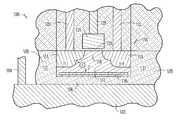
- FIG. 1illustrates an n-channel one transistor SOI non-volatile memory cell according to various embodiments of the present subject matter.
- the memory cell 100is formed on a substrate 102 , such as a silicon substrate, for example.
- the illustrationincludes a substrate contact 104 to contact the substrate 102 .
- the memory cell 100is isolated from the substrate 102 via a buried insulator, such as a buried oxide (BOX) layer 106 , and from other devices via shallow trench isolation (STI) regions 108 .
- a buried insulatorsuch as a buried oxide (BOX) layer 106
- STIshallow trench isolation
- a PD-SOI NFET 110is illustrated.
- the transistor 110includes a floating body region 112 , a first diffusion region 114 , and a second diffusion region 116 .
- a channel region 118is formed in the body region 112 between the first and second diffusion regions 114 and 116 .
- the body region 112is doped with p-type impurities, and the first and second diffusion regions 114 and 116 are doped with n+ impurities.
- the illustrated memory cell 100includes a bit line contact or drain contact 120 connected to the first diffusion region 114 , and a source line contact 122 connected to the second diffusion region 116 .
- a gate 124such as a polysilicon gate, is separated from the channel region 118 by a gate insulator region 126 .
- the illustrated memory cell 100includes a word line contact or gate contact 128 connected to the gate 124 .
- the body region 112 of the illustrated FET deviceincludes a charge trapping region 130 .
- Relatively simple fabrication techniquescan be used to incorporate the charge trapping region in the body region.
- the incorporation of the charge trapping region 130significantly improves scalability and functionality without complex fabrication techniques.
- the location of the charge trapping region 130 in the body region 112can be varied. In various embodiments, the location the charge trapping region 130 is on or near the BOX-body interface. In other embodiments, the charge trapping region 130 is located elsewhere in the body region 112 at a sufficient depth such that it will not interference with conductance. For example, various embodiments of the present subject matter position the charge trapping region 130 in the body region 112 at a depth below 200-300 ⁇ (20-30 nm) from the surface where the charge flows.
- the charge trapping region 130provides localized quantum wells that are initially neutral. These neutral wells attract charges and maintain the charge species. Thus, charge traps are distinguished from recombination centers, which have been proposed in a body region to assist with the recombination of charges. Unlike the charge trapping regions, a recombination center provides a charged localized quantum well. The charged well attracts opposite charges which recombine to facilitate charge neutrality.
- the charge trapping regionis capable of being tailored to provide the device with desired characteristics.
- various embodiments of the present subject matterare designed to repeatedly trap and de-trap charges in the charge trapping region so as to form a non-volatile random access memory.
- Various embodimentsprovide a charge trapping region with deep traps, and are designed to form a non-volatile, write once, read only memory.
- the charge trapping function of the charge trapping region 130is provided by a charge trapping layer.
- the charge trapping layerincludes a silicon-rich-insulator (SRI) layer, such as a silicon-rich-nitride (SRN) or silicon-rich-oxide (SRO) layer, for example.
- SRI, SRN and SROare described with respect to FIGS. 15 - 19 below in the section entitled Silicon Rich Insulators.
- SRI, SRN and SROare described with respect to FIGS. 15 - 19 below in the section entitled Silicon Rich Insulators.
- positive chargesare generated in the PD-SOI NFET due to impact ionization at the drain edge and alters the floating body potential.
- a part of these chargesare trapped by the charge trapping region 130 (e.g. SRN layer) in the body region 112 .
- the trapped chargeseffect the threshold voltage (V T ), and thus the channel conductance, of the PD-SOI-FET.
- the source current (I S ) of the PD-SOI-FETis used to determine if charges are trapped in the body region, and thus is used to determine the logic state of the memory cell.
- FIG. 2illustrates a p-channel one transistor SOI non-volatile memory cell according to various embodiments of the present subject matter.
- the body region 212is doped with n-type impurities, and the first and second diffusion regions 214 and 216 are doped with p+ impurities.
- Negative chargesare generated in the PD-SOI-PFET at the drain edge and alters the floating body potential. A part of these charges are trapped by the charge trapping region 230 (e.g. SRN layer) in the body region 212 .
- the trapped chargesaffect the threshold voltage (V T ), and thus the channel conductance, of the PD-SOI-PFET in a similar fashion to the PD-SOI-NFET.
- the source current (I S ) of the PD-SOI-PFETis used to determine if charges are trapped in the body region, and thus is used to determine the logic state of the memory cell.
- memory cells containing PD-SOI-NFET devicesare illustrated and described.
- One of ordinary skill in the artwill understand, upon reading and comprehending this disclosure, that the present subject matter is not limited to PD-SOI-NFET devices.
- FIG. 3illustrates a first memory read scheme according to various embodiments of the present subject matter.
- the state of the cell 300is sensed using a direct cell-current sense amplifier scheme.
- the memory cell 300is connected to the current sense circuitry 334 , which is used to sense the source current (I S ), and thus the state of the memory cell 300 .
- the schematic of the memory cellillustrates a capacitive coupling between the substrate and the PD-SOI-NFET of the memory cell.
- the BOX layer 106forms a dielectric between the substrate 102 and the body region 112 .
- an additional series capacitance 335is associated with the charge-trapping region.
- the charge trapping characteristicsis illustrated by dotted lines in the capacitor 335 .
- the direct cell-current sense amplifier schemecan be compared to the sensing schemes associated with static random access memory (SRAM).
- SRAMstatic random access memory
- FIG. 4illustrates a second memory read scheme according to various embodiments of the present subject matter.
- the state of the cell 400is sensed using a reference cell 436 and a current mode differential sense amplifier scheme. This scheme can be compared to the sensing schemes associated with dynamic random access memory (DRAM).
- DRAMdynamic random access memory
- Both the memory cell 400 and the reference cell 436are connected to the current sense circuitry 434 , which is used to compare the source current (I S ) of the memory cell 400 with the current (I REF ) of the reference cell 436 to determine the state of the memory cell 400 .
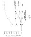
- FIG. 5illustrates electrical waveforms associated with reading a memory state “1” and a memory state “0” according to various embodiments of the present subject matter.
- a positive gate voltage (V G ) and a positive drain voltage (V D )are applied while the substrate voltage is held at a reference voltage (e.g. ground).
- V Gpositive gate voltage
- V Dpositive drain voltage
- the terms positive and negativeare relative terms with respect to the reference voltage.
- the threshold of the devicedecreases resulting in a higher source current (I S ), represented generally at 538 .
- I Ssource current
- the threshold of the deviceincreases resulting in a lower source current (I S ), represented generally at 540 .
- the difference between the source current in the memory state “1”can be two to three orders of magnitude greater than the source current in the memory state “0”.
- the one transistor SOI non-volatile memory cell of the present subjectexploits the body charging associated with the excess carriers in the body (also referred to as floating body effect) of PD-SOI devices to store information. Part of the excess carriers in the floating body gets trapped and stored in the charge trapping layer in the body. This trapped stored charge in the transistor body affects the threshold voltage (V T ). A lower threshold voltage (V T ) increases the source current (I S ) of the transistor, and a higher threshold voltage (V T ) decreases the source current (I S ). The source current (I S ) of the memory cell transistor is used to determine the state of the memory cell.
- a first method for generating charge in PD-SOI transistorsinvolves impact ionization in a field effect transistor (FET) operational mode.
- a second method for generating charge in PD-SOI transistorsinvolves a relatively low field parasitic bipolar junction transistor turn-on mode. These methods for generating charge are described in detail below with respect to a memory operation embodiment for n-channel FET devices.
- the excess charge for the NFET devicesare holes.
- One of ordinary skill in the artwill understand, upon reading and comprehending this disclosure, how to generate complementary charge (electrons) using the high field impact ionization mode and the relatively low field parasitic bipolar transistor mode for p-channel FET devices.
- the FET operational mode for generating charges in the body of a PD-SOI transistorinvolves high field impact ionization at the drain edge of the FET device.
- the generated positive charge in the body region of the PD-SOI-NFET deviceis directed toward the charge traps in the body region by providing an appropriate electromotive force (EMF) field vertical (or normal) to the FET channel.
- EMFelectromotive force
- the EMF fieldis provided by applying an appropriate voltage difference between the gate and the substrate.
- FIGS. 6 A- 6 Dillustrate a write operation for a memory cell in a FET mode of operation according to various embodiments of the present subject matter.
- a high positive drain voltage pulseis applied when the word line is held high such that the transistor operates in saturation (FIG. 6A).
- An excess of positive body charge 642is created near the drain region due to the impact ionization mechanism associated with the device operation in saturation (FIG. 6B).
- a negative substrate voltage pulseis applied (FIG. 6C) in a timely sequence after the positive charge is generated by the impact ionization mechanism.
- the negative substrate voltageprovides a EMF field across the body region which causes the generated holes 642 to drift toward the charge trapping region 630 (FIG. 6D).
- the charge trapping region 630includes a layer of SRN near the BOX/body interface. In this state, the raised positive body potential lowers the threshold voltage (V T ) of the transistor.
- FIGS. 7 A- 7 Billustrate an erase operation for a memory cell in an NFET-SOI mode of operation according to various embodiments of the present subject matter.
- a negative drain voltage pulseis applied to create an excess negative charge in the body.
- a positive substrate voltageis applied in a timely sequence.
- An EMF field 748is thereby set up from the substrate to the gate to attract the excess electrons toward the charge trapping region 730 which then neutralizes the trapped holes in the charge trapping region. The neutralization of the previously trapped positive charge lowers the body potential and consequently raises the threshold voltage (V T ) of the transistor.
- FIG. 8illustrates electrical waveforms associated with writing and erasing a memory cell in a FET mode of operation according to various embodiments of the present subject matter.
- a write 1 operation for a PD-SOI-NFET deviceinvolves generating excess holes and trapping the holes in the trapping layer of the body region of the device.
- the positive gate voltage pulse and the large drain voltage pulseshown within the dotted line 850 , causes the PD-SOI-NFET to turn on and operate in a saturated mode.
- An excess of positive charges (holes)are generated in the PD-SOI-NFET body due to impact ionization at the drain edge.
- the excess holes generated by impact ionizationare directed toward the charge trapping region due to the EMF field associated with the large negative substrate voltage pulse sequentially imposed in relationship of 850 and shown within the dotted line 852 .
- a write 0 operationalso referred to as an erase operation, for the PD-SOI-NFET device involves neutralizing the trapped holes with electrons generated in the body region of the device. Electrons are generated in the body region by forward biasing the p-n+junction using a negative drain pulse and a positive substrate pulse, shown within the dotted line 854 . The generated electrons drift toward the charge trapping region, where the electrons neutralize the stored holes.
- the positive substrate pulseextends for a duration longer than the negative drain pulse to provide an EMF field across the body that assists the drift of the generated electrons toward the charge trapping region.
- BJTBipolar Junction Transistor
- the lateral parasitic Bipolar Transistor mode for generating charges in the body of a PD-SOI transistorinvolves a relatively low field mechanism.
- the n-channel FET deviceincludes a parasitic lateral NPN bipolar junction transistor (BJT).
- BJTparasitic lateral NPN bipolar junction transistor
- Various voltagesare applied to the memory cell to cause the NPN transistor to generate positive charges (holes).
- the generated positive chargeis directed toward the charge trapping region in the body region by providing an appropriate electromotive force (EMF) field across the body by applying an appropriate voltage difference between the gate and the substrate.
- EMFelectromotive force
- FIGS. 9 A- 9 Billustrate a lateral parasitic bipolar junction transistor (BJT) associated with a FET device in the memory cell according to various embodiments of the present subject matter.
- the PD-SOI-NFET transistor 910includes a parasitic NPN transistor 956 , as illustrated in FIG. 9A.
- FIG. 9AOne of ordinary skill in the art will understand, upon reading and comprehending this disclosure, how to apply the teachings contained herein to a parasitic lateral PNP transistor in a PD-SOI-PFET transistor.
- FIG. 9Bis a schematic diagram of the memory cell of the present subject matter, and generally illustrates the parasitic BJT 956 in the PD-SOI-NFET transistor 910 .
- the substrate 902is capacitively coupled across the BOX layer 906 to the body region 912 of the NFET transistor, which also functions as the base of the parasitic NPN transistor.
- the body region 912includes charge trapping region 930 , such as an SRN charge trapping layer, for example.
- the body-substrate capacitor in the embodimentconsists of two series capacitors: the trapping layer capacitor and the BOX capacitor between the body and the substrate, as shown.
- FIGS. 10 A- 10 Dillustrate a write operation for a memory cell in a parasitic BJT mode of operation according to various embodiments of the present subject matter.
- a negative gate pulseis applied, and a negative drain pulse (having a shorter duration than the gate pulse) is applied during the negative gate pulse (FIG. 10A).
- the gate voltageis capacitively coupled simultaneously to the source and the body region while forward biasing the p-n+junction between the body region 1012 and the drain diffusion region 1014 .
- the lateral NPN transistor actiongenerates excess holes 1057 near the drain region 1014 of the PD-SOI-NFET (FIG. 10B).
- the substrateis pulsed negative (FIG. 10C).
- This negative substrate pulseprovides a vertical drift field 1058 through the body from the gate to the substrate (FIG. 10D).
- the vertical drift field 1058causes the generated holes 1057 to drift toward the charge trapping 1030 in the body of the transistor.
- the charge trapping regionstores at least a portion of the hole charges generated in the body region.
- FIGS. 11 A- 11 Billustrate an erase operation for a memory cell in a parasitic BJT mode of operation according to various embodiments of the present subject matter.
- the drain-body diode (n+-p)is forward biased by providing a negative drain pulse and a positive substrate pulse (FIG. 11A).
- the forward biased diodegenerates electrons 1146 in the body region (FIG. 1B).
- the gateis kept at a constant low positive potential as the substrate pulse is applied.
- the applied substrate pulseoverlaps the negative drain pulse.
- the positive substrate voltagecreates a vertical drift field 1148 to push the generated electrons 1146 toward the charge traps, which neutralizes the trapped holes in the body region of the PD-SOI-NFET device (FIG. 11B).
- FIG. 12illustrates electrical waveforms associated with writing and erasing a memory cell in a parasitic BJT mode of operation according to various embodiments of the present subject matter.
- a write 1 operation for a PD-SOI NFET deviceinvolves generating holes and trapping the holes in body region of the device.
- the negative gate voltage pulse and the large negative drain voltage pulseshown within the dotted line 1260 , causes the parasitic bipolar transistor to generate holes in the body region of the PD-SOI NFET. It is noted that the negative gate voltage pulse capacitively couples both the source and the body region, and the body region functions as the base of the parasitic BJT transistor.
- the body-drain junctionis forward biased because the drain voltage is more negative than the gate voltage.
- a large negative substrate voltage pulseshown within the dotted line 1262 , provides an EMF field that directs the generated holes toward the charge trapping region.
- a write 0 operation, also referred to as an erase operation, for the PD-SOI NFET deviceinvolves neutralizing the trapped holes with electrons generated in the body region of the device.
- a small positive voltage, illustrated by the dotted line 1264is applied to the gate.
- Electronsare generated in the body region by forward biasing the p-n+junction using a negative drain pulse and a positive substrate pulse, shown within the dotted line 1266 .
- the electron driftis toward the charge traps, where the electrons neutralize the stored holes.
- the positive substrate pulseextends for a duration longer than the negative drain pulse, allowing the substrate pulse and the gate potential to provide an EMF field that assists the drift of the generated electrons toward the charge centers of the charge trapping region (charge trapping layer).
- the memory cellis fully scalable.
- the functionality of the memory cellis independent of the feature size.
- the cell densitydirectly benefits from the reduction in feature size.
- this memory cellimproves in functionality and characteristics as the feature size is reduced due to the following reasons.
- One reasonis that the device short channel effect improves due to the reduction in the volume of neutral region of the body and due to the “narrow-width-effect” that raises the “base” threshold of the device.
- charge trapping efficiencyis improved due to the increase in carrier energy of the excess carriers as the body volume is reduced.
- the device leakageis also reduced due to both of these reasons. Additionally, trapped charges extend the body depletion regions, reducing device parasitic capacitance. This further improves intrinsic device switching speed.
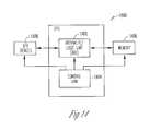
- FIG. 13is a simplified block diagram of a high-level organization of various embodiments of a memory device according to various embodiments of the present subject matter.
- the illustrated memory device 1368includes a memory array 1370 and read/write control circuitry 1372 to perform operations on the memory array via communication line(s) 1374 .
- the memory array 1370includes a number of one transistor SOI non-volatile memory cells 1300 as described above.
- the illustrated memory cells 1300include PD-SOI NFET devices, the present subject matter is not limited to PD-SOI-NFET devices.
- the memory cells in the arrayare arranged in rows and columns.
- word linesconnect the memory cells in the rows
- bit linesconnect the memory cells in the columns.
- the memory cells in the arrayare formed in a single substrate.
- the substrate for one or more memory cellsis isolated from the substrate(s) for other memory cells. Thus, these embodiments provide the ability to provide different substrate voltages to different portions of the memory array.
- the read/write control circuitry 1372includes word line select and power circuitry 1374 , which functions to select a desired row and to provide a desired power signal or pulse to the selected row.
- the read/write control circuitry 1372further includes bit line select and power circuitry 1376 , which functions to select a desired column and to provide a desired power signal or pulse to the selected column.
- the read/write control circuitry 1372further includes substrate potential control circuitry 1378 which functions to provide a desired power signal or pulse to the substrate. According to various embodiments in which the memory array includes a number of isolated substrates, the substrate potential control circuitry 1378 also functions to select a desired substrate to which the desired power signal or pulse is applied.
- the read/write control circuitry 1372further includes read circuitry 1380 , which functions to detect a memory state for a selected memory cell in the memory array 1370 .
- the read circuitry 1380uses a direct cell-current sense amplifier scheme such as that illustrated in FIG. 3.
- the read circuitry 1380uses a reference cell and a current mode differential sense amplifier scheme such as that illustrated in FIG. 4.
- FIG. 14is a simplified block diagram of a high-level organization of various embodiments of an electronic system according to the present subject matter.
- the system 1400is a computer system, a process control system or other system that employs a processor and associated memory.
- the electronic system 1400has functional elements, including a processor or arithmetic/logic unit (ALU) 1402 , a control unit 1404 , a memory device unit 1406 and an input/output (I/O) device 1408 .
- ALUarithmetic/logic unit
- the control unit 1404coordinates all operations of the processor 1402 , the memory device 1406 and the I/O devices 1408 by continuously cycling through a set of operations that cause instructions to be fetched from the memory device 1406 and executed.
- the memory device 1406includes, but is not limited to, random access memory (RAM) devices, read-only memory (ROM) devices, and peripheral devices such as a floppy disk drive and a compact disk CD-ROM drive.
- RAMrandom access memory
- ROMread-only memory
- peripheral devicessuch as a floppy disk drive and a compact disk CD-ROM drive.
- any of the illustrated electrical componentsare capable of being fabricated to include one-transistor, non-volatile SOI memory cells in accordance with the present subject matter.
- the illustration of the system 1400is intended to provide a general understanding of one application for the structure and circuitry of the present subject matter, and is not intended to serve as a complete description of all the elements and features of an electronic system using one-transistor, SOI non-volatile memory cells according to the present subject matter.
- an electronic systemcan be fabricated in single-package processing units, or even on a single semiconductor chip, in order to reduce the communication time between the processor and the memory device.
- Applications containing one-transistor, SOI non-volatile memory cellsinclude electronic systems for use in memory modules, device drivers, power modules, communication modems, processor modules, and application-specific modules, and may include multilayer, multichip modules.
- Such circuitrycan further be a subcomponent of a variety of electronic systems, such as a clock, a television, a cell phone, a personal computer, an automobile, an industrial control system, an aircraft, and others.
- a silicon-rich-insulatorsuch as a silicon-rich-nitride (SRN) or silicon-rich-oxide (SRO) is used to provide charge traps in the body region of PD-SOI-FET devices.
- SRIsilicon-rich-insulator
- SRNsilicon-rich-nitride
- SROsilicon-rich-oxide
- a layer of SRIis formed in the body region near an interface between the body region and the BOX layer.
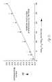
- FIG. 15is a graph showing refractive index of silicon-rich silicon nitride films versus SiH 2 Cl 2 /NH 3 flow rate ratio (R). This graph is provided herein to illustrate the relationship between the silicon amount and the refractive index. The graph indicates that the index of refraction increases linearly with increasing silicon content. As such, the index of refraction of the films can be used as an indication of the silicon content of the films.
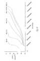
- FIG. 16is a graph showing current density versus applied field for silicon-rich silicon nitride films having different percentages of excess silicon.
- the current density (J)is represented in amperes/cm 2
- log Jis plotted against the electric field E (volts/cm) for Si 3 N 4 layers having a SiH 2 Cl 2 /NH 3 flow rate ratio R of 0.1, 3, 5, 10, 15 and 31.
- This graphis provided herein to illustrate the relationship between the amount of silicon and the conductivity of the film.
- FIG. 17is a graph showing flatband shift versus time at an applied field of 4 ⁇ 10 6 volts/cm for silicon-rich silicon nitride films having varying percentages of excess silicon.
- R3
- the flatband shiftis greater than the shifts produced by films having an R of 0.1, 10 or 15.
- the film having an R of 10provides a greater flatband shift than a film having an R of 15 .
- FIGS. 17 and 18are provided to illustrate the characteristics of a charge storing medium and a more conductive charge injector medium as further explained below.
- Silicon-rich silicon nitride films deposited at an R of 3 or 5will possess a charge storing function or property normally provided by a polysilicon floating gate of a EEPROM cell.
- silicon-rich nitride films having an R greater than 0.1 and less than 10or, more specifically, having an index of refraction between approximately 2.10 and 2.30
- This charge trappingis characteristic of a charge storing medium that can be used as a charge trapping material in the present subject matter.
- Silicon-rich nitride films having an R greater than 10are referred to as an injector medium.
- FIG. 19is a graph showing apparent dielectric constant K versus refractive index for both Silicon Rich Nitride (SRN) and Silicon Rich Oxide (SRO).
- SRNSilicon Rich Nitride
- SROSilicon Rich Oxide
- the SRO and SRO plotted in this graphwere provided using a Low Pressure Chemical Vapor Deposition (LPCVD) process.
- the SROwas fabricated at approximately 680° C., and the fabricated structure included 100 ⁇ oxide and 150 ⁇ SRO.
- the SRNwas fabricated at approximately 770° C., and the fabricated structure included 45 ⁇ oxide and 80 ⁇ SRN.
- the dielectric constant of siliconis around 12. Materials with a higher K than silicon are conventionally termed a high K material, and materials with a lower K than silicon are conventionally termed a low K material.
- Injector SRIincludes these high K SRO and high K SRN.
- Charge-centered SRIincludes low K SRO and low K SRN.
- the processing of the memory cell of the present subject matterinvolves standard processing associated with PD-SOI device fabrication.
- the channel implantis adjusted to appropriately tailor the FET threshold.
- the BOX-body interfaceincludes a trapping layer, such as an SRI layer.
- Various embodimentscreate the trapping layer using the following process. Standard processing steps are performed through the shallow trench isolation (STI). A block mask is applied to device and open the active retention of the FET device.
- the FET deviceis an NFET device, but the present subject matter is not limited to NFET devices.
- Silicon, ammonia (NH 3 ), and optionally hydrogenare ion implanted with an appropriate energy and concentration to achieve a desired refractive index after post processing anneal.
- ammoniais replaced by active nitrogen.
- siliconis replaced by other active silicon sources such as silane, dichlorosilane, and the like.
- a post-implant inert annealis performed.
- the annealincludes a rapid thermal anneal (RTA).
- RTArapid thermal anneal
- the annealincludes an inert plasma anneal in nitrogen.
- Standard PD-SOI CMOS fabrication stepsare capable of being performed thereafter to complete the fabrication of the memory cell.
- charge trapping layersare specifically cited as “charge trapping layers,” many other charge trapping materials are used as a charge trapping medium in many other embodiments.
- charge trapping materialsfor example, transition-metal-oxides, metal silicides and composites or laminates can be used to form charge trapping layers.
- Nano-voidsalso can be used to form charge trapping layers. These examples are not intended to be an exhaustive list of the number of ways to form charge trapping layers that can be used according to the present subject matter. One of ordinary skill in the art will understand that such layers are incorporated by appropriate fabrication processes.
- the present subject matterrelates to non-volatile SOI memory cells.
- the present subject matterexploits the floating body effect associated with SOI-FET devices.
- the memory cellincludes charge trapping regions in the body region of a SOI-FET device. Charges generated by the floating body effect are stored in the charge trapping regions to provide a first memory state, and the stored charges are neutralized to provide a second memory state.
- the threshold voltage of the SOI-FETis affected by the stored charges.
- the channel conductanceis capable of being used to determine the state of the memory cell.
- the present subject matteris capable of providing non-volatile memories. Memories according to the present subject matter are capable of maintaining data integrity for up to ten years without refresh. Additionally, the present subject matter is capable of providing non-volatile memories that can be written using the power supply voltage. Thus, the present subject matter does not require the complicated circuitry to generate and deliver 4 to 8 times the power supply voltage such as is required by Flash, EEPROM and the like. Additionally, the present subject matter is capable of providing memories with an effectively unlimited number of write-erase cycles during the system lifetime (10 13 to 10 14 write-erase cycles in 10 years). Additionally, the present subject matter is capable of providing memories that have fast read and write operations on the order of nanoseconds rather than milliseconds. Additionally, the present subject matter is capable of providing dense memories (4F 2 ).
Landscapes
- Engineering & Computer Science (AREA)
- Microelectronics & Electronic Packaging (AREA)
- Semiconductor Memories (AREA)
- Non-Volatile Memory (AREA)
- Thin Film Transistor (AREA)
Abstract
Description
- This application is related to the following commonly assigned U.S. patent applications which are herein incorporated by reference in their entirety: “Scalable Flash/NV Structures & Devices With Enhanced Endurance,” U.S. application Ser. No. 09/944,985, filed on Aug. 30, 2001; “Stable PD-SOI Devices and Methods,” U.S. application Ser. No. 10/197,978, filed on Jul. 18, 2002; “Gated Lateral Thyristor-Based Random Access Memory Cell (GLTRAM),” U.S. application Ser. No. ______, filed on (Attorney Docket No. 1303.072US1); and “One-Device Non-Volatile Random Access Memory Cell,” U.S. application Ser. No. ______, filed on (Attorney Docket No. 1303.073US11).[0001]
- This disclosure relates generally to integrated circuits, and more particularly, to non-volatile, silicon-on-insulator (SOI) memory cells.[0002]
- Known dynamic random access memory (DRAM) devices include a switching transistor and an integrated storage capacitor tied to the storage node of the transistor. Incorporating a stacked capacitor or a trench capacitor in parallel with the depletion capacitance of the floating storage node enhances charge storage. Due to a finite charge leakage across the depletion layer, the capacitor is frequently recharged or refreshed to ensure data integrity in the DRAM device. Thus, such a DRAM device is volatile. A power failure causes permanent data loss in a DRAM device. DRAM devices are relatively inexpensive, power efficient, and fast compared to non-volatile random access memory (NVRAM) devices.[0003]
- A minimum capacitance per cell is required to sense a conventional DRAM cell. A significant challenge for every succeeding generation of reduced feature size is to provide this minimum capacitance per cell. A memory cell design goal is to achieve an 8F[0004]2DRAM cell. To that end, complex three-dimensional capacitor structures have been designed. However, these complex three-dimensional capacitor structures are difficult to manufacture and adversely impact yield. There has been serious concern of the scalability of the conventional DRAM cell beyond the 0.1 μm lithographic generation. The scaling problems have been aggravated by increased device short channel effects and leakages associated with complicated capacitor structures. Thus, the elimination of the stacked capacitor or trench capacitor in a DRAM cell is desirable.
- A silicon-on-insulator (SOI) capacitor-less single-transistor DRAM cell has been proposed by S.Okhonin et al. The state of the floating body charge in the transistor affects the channel conductance of the transistor and defines the memory state (“1” or “0”) of the cell. Two methods for generating carriers in the body were proposed. The generated carriers are holes for the partially depleted (PD) SOI-NFET or electrons for the PD-SOI-PFET. One proposed method generates carriers using the drain-edge high field effect associated with impact ionization. In another case, the carriers are generated by the parasitic bipolar phenomenon.[0005]
- The memory retention for these SOI capacitor-less single-transistor DRAM cells depends on the device channel length. That is, the stored charge retention time decreases with decreasing channel length. Additionally, the memory retention depends on recombination charge constants and multiple recombination mechanisms, and thus is expected to be both temperature and process sensitive. Therefore, controlling the memory retention between refresh operations is expected to be difficult.[0006]
- Known non-volatile random access memory (NVRAM), such as Flash, EPROM, EEPROM, etc., store charge using a floating gate or a floating plate. Charge trapping centers and associated potential wells are created by forming nano-particles of metals or semiconductors in a large band gap insulating matrix, or by forming nano-layers of metal, semiconductor or a small band gap insulator that interface with one or more large band gap insulating layers. The floating plate or gate can be formed as an integral part of the gate insulator stack of the switching transistor.[0007]
- Field emission across the surrounding insulator causes the stored charge to leak. The stored charge leakage from the floating plate or floating gate is negligible for non-volatile memory devices because of the high band gap insulator. For example, silicon dioxide (SiO[0008]2) has a 9 ev band gap, and oxide-nitride-oxide (ONO) and other insulators have a band gap in the range of 4.5 ev to 9 ev. Thus, the memory device retains stored data throughout a device's lifetime.
- However, there are problems associated with NVRAM devices. The writing process, also referred to as “write-erase programming,” for non-volatile memory is slow and energy inefficient, and requires complex high voltage circuitry for generating and routing high voltage. Additionally, the write-erase programming for non-volatile memory involves high-field phenomena (hot carrier or field emission) that degrades the surrounding insulator. The degradation of the insulator eventually causes significant leakage of the stored charge. Thus, the high-field phenomena negatively affects the endurance (the number of write/erase cycles) of the NVRAM devices. The number of cycles of writing and erasing is typically limited to 1 E6 cycles. Therefore, the available applications for these known NVRAM devices is limited.[0009]
- Floating plate non-volatile memory devices have been designed that use a gate insulator stack with silicon-rich insulators. In these devices, injected charges (electrons or holes) are trapped and retained in local quantum wells provided by nano-particles of silicon embedded in a matrix of a high band gap insulator (also referred to as a “trapless” or “limited trap” insulator) such as silicon dioxide (SiO[0010]2) or silicon nitride (Si3N4). In addition to silicon trapping centers, other trapping centers include tungsten particles embedded in SiO2, gold particles embedded in SiO2, and a tungsten oxide layer embedded in SiO2.
- There is a need in the art to provide dense and high speed capacitor-less memory cells with data non-volatility similar to Flash devices and DRAM-like endurance as provided by the present subject matter.[0011]
- The above mentioned problems are addressed by the present subject matter and will be understood by reading and studying the following specification. The present subject matter relates to non-volatile memory cells. In various embodiments, the memory cells are formed using one transistor. In various embodiments, the memory cell transistor is a partially-depleted SOI field effect transistor (PD-SOI-FET) transistor with a floating body that contains charge traps.[0012]
- The present subject matter provides a binary memory state by trapping charges in the floating body to provide a first state and by neutralizing and/or de-trapping the trapped charges in the floating body to provide a second state. Both states are stable to provide non-volatility. Various embodiments provide a charge trapping region in the body of the transistor near the interface between the transistor body and the buried insulator, such as buried oxide (BOX). Various embodiments provide a charge trapping layer, such as a silicon-rich-nitride (SRN) layer, near the BOX-body interface. The charges are neutralized by providing charges of opposite polarity into the transistor body. Charge retention is independent with respect to the device body length. The memory cell of the present subject matter is capable of long charge retention and non-volatility. Additionally, the memory cell of the present subject matter provides high density (4F[0013]2) and fast DRAM-like read-write capabilities.
- One aspect of the present subject matter relates to a memory cell. In various embodiments, the memory cell includes a substrate, a buried insulator layer formed on the substrate, and a transistor formed on the buried insulator layer. The transistor includes a floating body region that includes a charge trapping material (or charge trapping region). A memory state of the memory cell is determined by trapped charges or neutralized charges in the charge trapping material. The transistor further includes a first diffusion region and a second diffusion region to provide a channel region in the body region between the first diffusion region and the second diffusion region. The transistor further includes a gate insulator layer formed over the channel region, and a gate formed over the gate insulator layer.[0014]
- These and other aspects, embodiments, advantages, and features will become apparent from the following description of the present subject matter and the referenced drawings.[0015]
- FIG. 1 illustrates an n-channel one transistor SOI non-volatile memory cell according to various embodiments of the present subject matter.[0016]
- FIG. 2 illustrates a p-channel one transistor SOI non-volatile memory cell according to various embodiments of the present subject matter.[0017]
- FIG. 3 illustrates a first memory read scheme according to various embodiments of the present subject matter.[0018]
- FIG. 4 illustrates a second memory read scheme according to various embodiments of the present subject matter.[0019]
- FIG. 5 illustrates electrical waveforms associated with reading a memory state “1” and a memory state “0” according to various embodiments of the present subject matter.[0020]
- FIGS.[0021]6A-6D illustrate a write operation for a memory cell in a FET mode of operation according to various embodiments of the present subject matter.
- FIGS.[0022]7A-7B illustrate an erase operation for a memory cell in a FET mode of operation according to various embodiments of the present subject matter.
- FIG. 8 illustrates electrical waveforms associated with writing and erasing a memory cell in a FET mode of operation according to various embodiments of the present subject matter.[0023]
- FIGS.[0024]9A-9B illustrate a lateral parasitic bipolar junction transistor (BJT) associated with a FET device in the memory cell according to various embodiments of the present subject matter.
- FIGS.[0025]10A-10D illustrate a write operation for a memory cell in a parasitic BJT mode of operation according to various embodiments of the present subject matter.
- FIGS.[0026]11A-11B illustrate an erase operation for a memory cell in a parasitic BJT mode of operation according to various embodiments of the present subject matter.
- FIG. 12 illustrates electrical waveforms associated with writing and erasing a memory cell in a parasitic bipolar mode of operation according to various embodiments of the present subject matter.[0027]
- FIG. 13 is a simplified block diagram of a high-level organization of various embodiments of a memory device according to various embodiments of the present subject matter.[0028]
- FIG. 14 is a simplified block diagram of a high-level organization of various embodiments of an electronic system according to the present subject matter.[0029]
- FIG. 15 is a graph showing refractive index of silicon-rich silicon nitride films versus SiH[0030]2Cl2/NH3flow rate ratio.
- FIG. 16 is a graph showing current density versus applied field for silicon-rich silicon nitride films having different percentages of excess silicon.[0031]
- FIG. 17 is a graph showing flat band shift versus time at an applied field of 4×10[0032]6volts/cm for silicon-rich silicon nitride films having varying percentages of excess silicon.
- FIG. 18 is a graph showing flat band shift versus time at an applied field of 7×10[0033]6volts/cm for silicon-rich silicon nitride films having varying percentages of excess silicon.
- FIG. 19 is a graph showing apparent dielectric constant K versus refractive index for both Silicon Rich Nitride (SRN) and Silicon Rich Oxide (SRO).[0034]
- The following detailed description refers to the accompanying drawings which show, by way of illustration, specific aspects and embodiments in which the present subject matter may be practiced. These embodiments are described in sufficient detail to enable those skilled in the art to practice the present subject matter. The various embodiments of the present subject matter are not necessarily mutually exclusive. Other embodiments may be utilized and structural, logical, and electrical changes may be made without departing from the scope of the present subject matter. In the following description, the terms wafer and substrate are interchangeably used to refer generally to any structure on which integrated circuits are formed, and also to such structures during various stages of integrated circuit fabrication. Both terms include doped and undoped semiconductors, epitaxial layers of a semiconductor on a supporting semiconductor or insulating material, combinations of such layers, as well as other such structures that are known in the art. The term “horizontal” as used in this application is defined as a plane parallel to the conventional plane or surface of a wafer or substrate, regardless of the orientation of the wafer or substrate. The term “vertical” refers to a direction perpendicular to the horizontal as defined above. Prepositions, such as “on”, “side” (as in sidewall), “higher”, “lower”, “over” and “under” are defined with respect to the conventional plane or surface being on the top surface of the wafer or substrate, regardless of the orientation of the wafer or substrate. The following detailed description is, therefore, not to be taken in a limiting sense, and the scope of the present invention is defined only by the appended claims, along with the full scope of equivalents to which such claims are entitled.[0035]
- The present subject matter relates to a one transistor, non-volatile memory cell. The memory cell is formed using silicon-on-insulator (SOI) technology. In various embodiments, the memory cell transistor is a partially-depleted SOI field effect transistor (PD-SOI-FET) with a floating body that contains charge traps. However, various embodiments of the present subject matter include other floating body transistors.[0036]
- The one transistor SOI memory cell of the present subject matter achieves high density (4F[0037]2), has fast DRAM-like read/write capabilities, and has high-retention and non-volatility. A binary yet stable memory state is provided by trapping charges in the floating body of the PD-SOI transistor, and by neutralizing (or discharging) the charges trapped in the floating body. In various embodiments, the trapped charge is neutralized by injecting charge of opposite polarity into the body. The state of the memory cell is read by sensing the channel conductance of the cell transistor to determine if the cell transistor is in a charged state or a neutralized state, which can be defined as a logic or memory state “1”, and a logic or memory state “0”. For example, the memory cell state is determined by sensing the change in the device current that is associated with the trapped stored-charge.
- The present subject matter generates carriers in a floating body of the PD-SOI transistor, and traps the carriers in the floating body using charge traps. The binary memory state is provided by trapping charges in the floating body and by neutralizing the trapped charge in the floating body. In various embodiments, the charge traps are provided by a charge trapping layer in the floating body. According to various embodiments, the charge trapping layer includes silicon-rich-nitride (SRN). The trapped carriers are neutralized by generating and injecting charges of opposite polarity.[0038]
- According to various embodiments, the memory cell provides an energy barrier for the stored charge in the order of 1 ev or less. Thus, for various embodiments, the memory cell is capable of having long charge retention for both the charged state and the neutralized state. The charge retention is independent of the channel length. This long charge retention provides the memory cell with a non-volatile characteristic. The degree of non-volatility can be altered by altering the trapping material and thereby modifying the energy barrier (trapped energy depth). Therefore, various embodiments have an appropriate trapping material to provide a non-volatile random access memory, and various embodiments have an appropriate trapping material to provide a non-volatile write once, read only memory.[0039]
- Those of ordinary skill in the art will appreciate, upon reading and understanding this disclosure, that the present subject matter provides a number of benefits. These benefits include inexpensive and dense memories. The memory cell (4F[0040]2) of the present invention is twice as dense as a conventional DRAM (8F2). Another benefit is non-volatility, thus eliminating the need to refresh the state of the memory cell. Another benefit of the present subject matter is that the memory cell of the present subject matter is energy efficient. Another benefit is that the present subject matter provides DRAM-like endurance within a non-volatile memory cell because the non-volatile memory cell of the present subject matter is capable of undergoing a large number of write/erase cycles.
- Memory Cell Structure[0041]
- FIG. 1 illustrates an n-channel one transistor SOI non-volatile memory cell according to various embodiments of the present subject matter. The[0042]
memory cell 100 is formed on asubstrate 102, such as a silicon substrate, for example. The illustration includes asubstrate contact 104 to contact thesubstrate 102. Thememory cell 100 is isolated from thesubstrate 102 via a buried insulator, such as a buried oxide (BOX)layer 106, and from other devices via shallow trench isolation (STI)regions 108. - A PD-SOI NFET[0043]110 is illustrated. The transistor110 includes a floating
body region 112, afirst diffusion region 114, and asecond diffusion region 116. Achannel region 118 is formed in thebody region 112 between the first andsecond diffusion regions body region 112 is doped with p-type impurities, and the first andsecond diffusion regions memory cell 100 includes a bit line contact ordrain contact 120 connected to thefirst diffusion region 114, and asource line contact 122 connected to thesecond diffusion region 116. A gate124, such as a polysilicon gate, is separated from thechannel region 118 by agate insulator region 126. The illustratedmemory cell 100 includes a word line contact orgate contact 128 connected to the gate124. - Unlike conventional FET devices, the[0044]
body region 112 of the illustrated FET device includes acharge trapping region 130. Relatively simple fabrication techniques can be used to incorporate the charge trapping region in the body region. However, as one of ordinary skill in the art will understand upon reading and comprehending this disclosure, the incorporation of thecharge trapping region 130 significantly improves scalability and functionality without complex fabrication techniques. - The location of the[0045]
charge trapping region 130 in thebody region 112 can be varied. In various embodiments, the location thecharge trapping region 130 is on or near the BOX-body interface. In other embodiments, thecharge trapping region 130 is located elsewhere in thebody region 112 at a sufficient depth such that it will not interference with conductance. For example, various embodiments of the present subject matter position thecharge trapping region 130 in thebody region 112 at a depth below 200-300 Å (20-30 nm) from the surface where the charge flows. - The[0046]
charge trapping region 130 provides localized quantum wells that are initially neutral. These neutral wells attract charges and maintain the charge species. Thus, charge traps are distinguished from recombination centers, which have been proposed in a body region to assist with the recombination of charges. Unlike the charge trapping regions, a recombination center provides a charged localized quantum well. The charged well attracts opposite charges which recombine to facilitate charge neutrality. - One of ordinary skill in the art will understand, upon reading and comprehending this disclosure, that the charge trapping region is capable of being tailored to provide the device with desired characteristics. For example, various embodiments of the present subject matter are designed to repeatedly trap and de-trap charges in the charge trapping region so as to form a non-volatile random access memory. Various embodiments provide a charge trapping region with deep traps, and are designed to form a non-volatile, write once, read only memory.[0047]
- In various embodiments, the charge trapping function of the[0048]
charge trapping region 130 is provided by a charge trapping layer. According to various embodiments, the charge trapping layer includes a silicon-rich-insulator (SRI) layer, such as a silicon-rich-nitride (SRN) or silicon-rich-oxide (SRO) layer, for example. SRI, SRN and SRO are described with respect to FIGS.15-19 below in the section entitled Silicon Rich Insulators. One of ordinary skill in the art will understand, upon reading and comprehending this disclosure, that many other materials or combination of layers may be selected that provide the desired energy barriers, and thus provide the desired charge trapping characteristics. - As will be described in more detail below, positive charges (holes) are generated in the PD-SOI NFET due to impact ionization at the drain edge and alters the floating body potential. In this embodiment a part of these charges are trapped by the charge trapping region[0049]130 (e.g. SRN layer) in the
body region 112. The trapped charges effect the threshold voltage (VT), and thus the channel conductance, of the PD-SOI-FET. According to various embodiments, the source current (IS) of the PD-SOI-FET is used to determine if charges are trapped in the body region, and thus is used to determine the logic state of the memory cell. - FIG. 2 illustrates a p-channel one transistor SOI non-volatile memory cell according to various embodiments of the present subject matter. One of ordinary skill in the art, upon reading and comprehending this disclosure, will understand the structural similarities between the PD-SOI-PFET device and the PD-SOI-NFET device. Some of these structural similarities are not addressed again here for the purpose of simplifying the disclosure.[0050]
- With respect to the illustrated PD-SOI-PFET, the[0051]
body region 212 is doped with n-type impurities, and the first andsecond diffusion regions body region 212. The trapped charges affect the threshold voltage (VT), and thus the channel conductance, of the PD-SOI-PFET in a similar fashion to the PD-SOI-NFET. According to various embodiments, the source current (IS) of the PD-SOI-PFET is used to determine if charges are trapped in the body region, and thus is used to determine the logic state of the memory cell. - In order to simplify this disclosure, memory cells containing PD-SOI-NFET devices are illustrated and described. One of ordinary skill in the art will understand, upon reading and comprehending this disclosure, that the present subject matter is not limited to PD-SOI-NFET devices.[0052]
- FIG. 3 illustrates a first memory read scheme according to various embodiments of the present subject matter. In the illustrated[0053]
system 332, the state of thecell 300 is sensed using a direct cell-current sense amplifier scheme. Thememory cell 300 is connected to thecurrent sense circuitry 334, which is used to sense the source current (IS), and thus the state of thememory cell 300. The schematic of the memory cell illustrates a capacitive coupling between the substrate and the PD-SOI-NFET of the memory cell. As shown in FIG. 1, theBOX layer 106 forms a dielectric between thesubstrate 102 and thebody region 112. Aside from the gate-body and body substrate capacitance333 shown in FIG. 3, anadditional series capacitance 335 is associated with the charge-trapping region. The charge trapping characteristics is illustrated by dotted lines in thecapacitor 335. - The direct cell-current sense amplifier scheme can be compared to the sensing schemes associated with static random access memory (SRAM). One of ordinary skill in the art will understand, upon reading and comprehending this disclosure, that the memory cell can be designed and the performance of the memory cell specified such that the direct cell-current sense amplifier scheme can be used.[0054]
- FIG. 4 illustrates a second memory read scheme according to various embodiments of the present subject matter. In the illustrated[0055]
system 432, the state of thecell 400 is sensed using areference cell 436 and a current mode differential sense amplifier scheme. This scheme can be compared to the sensing schemes associated with dynamic random access memory (DRAM). Both thememory cell 400 and thereference cell 436 are connected to thecurrent sense circuitry 434, which is used to compare the source current (IS) of thememory cell 400 with the current (IREF) of thereference cell 436 to determine the state of thememory cell 400. - FIG. 5 illustrates electrical waveforms associated with reading a memory state “1” and a memory state “0” according to various embodiments of the present subject matter. For the illustrated read operations, a positive gate voltage (V[0056]G) and a positive drain voltage (VD) are applied while the substrate voltage is held at a reference voltage (e.g. ground). One of ordinary skill in the art will understand, upon reading and comprehending this disclosure, that the terms positive and negative are relative terms with respect to the reference voltage.
- When the memory cell is in a memory state “1” in which holes are stored in the charge trapping region within the floating body of the PD-SOI NFET device, the threshold of the device decreases resulting in a higher source current (I[0057]S), represented generally at538. When the memory cell is in a memory state “0” in which the stored holes are neutralized in the floating body of the PD-SOI NFET device, the threshold of the device increases resulting in a lower source current (IS), represented generally at540. The difference between the source current in the memory state “1” can be two to three orders of magnitude greater than the source current in the memory state “0”.
- Memory Cell Operation[0058]
- The one transistor SOI non-volatile memory cell of the present subject exploits the body charging associated with the excess carriers in the body (also referred to as floating body effect) of PD-SOI devices to store information. Part of the excess carriers in the floating body gets trapped and stored in the charge trapping layer in the body. This trapped stored charge in the transistor body affects the threshold voltage (V[0059]T). A lower threshold voltage (VT) increases the source current (IS) of the transistor, and a higher threshold voltage (VT) decreases the source current (IS). The source current (IS) of the memory cell transistor is used to determine the state of the memory cell.
- There are a number of ways in which to generate the excess charge in a PD-SOI transistor. A first method for generating charge in PD-SOI transistors involves impact ionization in a field effect transistor (FET) operational mode. A second method for generating charge in PD-SOI transistors involves a relatively low field parasitic bipolar junction transistor turn-on mode. These methods for generating charge are described in detail below with respect to a memory operation embodiment for n-channel FET devices. The excess charge for the NFET devices are holes. One of ordinary skill in the art will understand, upon reading and comprehending this disclosure, how to generate complementary charge (electrons) using the high field impact ionization mode and the relatively low field parasitic bipolar transistor mode for p-channel FET devices.[0060]
- FET Mode of Operation[0061]
- The FET operational mode for generating charges in the body of a PD-SOI transistor involves high field impact ionization at the drain edge of the FET device. In various embodiments, the generated positive charge in the body region of the PD-SOI-NFET device is directed toward the charge traps in the body region by providing an appropriate electromotive force (EMF) field vertical (or normal) to the FET channel. The EMF field is provided by applying an appropriate voltage difference between the gate and the substrate.[0062]
- FIGS.[0063]6A-6D illustrate a write operation for a memory cell in a FET mode of operation according to various embodiments of the present subject matter. In the FET operational mode, a high positive drain voltage pulse is applied when the word line is held high such that the transistor operates in saturation (FIG. 6A). An excess of
positive body charge 642 is created near the drain region due to the impact ionization mechanism associated with the device operation in saturation (FIG. 6B). A negative substrate voltage pulse is applied (FIG. 6C) in a timely sequence after the positive charge is generated by the impact ionization mechanism. The negative substrate voltage provides a EMF field across the body region which causes the generatedholes 642 to drift toward the charge trapping region630 (FIG. 6D). In various embodiments, thecharge trapping region 630 includes a layer of SRN near the BOX/body interface. In this state, the raised positive body potential lowers the threshold voltage (VT) of the transistor. - FIGS.[0064]7A-7B illustrate an erase operation for a memory cell in an NFET-SOI mode of operation according to various embodiments of the present subject matter. A negative drain voltage pulse is applied to create an excess negative charge in the body. Additionally, a positive substrate voltage is applied in a timely sequence. An
EMF field 748 is thereby set up from the substrate to the gate to attract the excess electrons toward thecharge trapping region 730 which then neutralizes the trapped holes in the charge trapping region. The neutralization of the previously trapped positive charge lowers the body potential and consequently raises the threshold voltage (VT) of the transistor. - FIG. 8 illustrates electrical waveforms associated with writing and erasing a memory cell in a FET mode of operation according to various embodiments of the present subject matter. A[0065]
write 1 operation for a PD-SOI-NFET device involves generating excess holes and trapping the holes in the trapping layer of the body region of the device. The positive gate voltage pulse and the large drain voltage pulse, shown within the dottedline 850, causes the PD-SOI-NFET to turn on and operate in a saturated mode. An excess of positive charges (holes) are generated in the PD-SOI-NFET body due to impact ionization at the drain edge. The excess holes generated by impact ionization are directed toward the charge trapping region due to the EMF field associated with the large negative substrate voltage pulse sequentially imposed in relationship of850 and shown within the dottedline 852. - According to various embodiments, a[0066]
write 0 operation, also referred to as an erase operation, for the PD-SOI-NFET device involves neutralizing the trapped holes with electrons generated in the body region of the device. Electrons are generated in the body region by forward biasing the p-n+junction using a negative drain pulse and a positive substrate pulse, shown within the dottedline 854. The generated electrons drift toward the charge trapping region, where the electrons neutralize the stored holes. The positive substrate pulse extends for a duration longer than the negative drain pulse to provide an EMF field across the body that assists the drift of the generated electrons toward the charge trapping region. - Bipolar Junction Transistor (BJT) Mode of Operation[0067]
- The lateral parasitic Bipolar Transistor mode for generating charges in the body of a PD-SOI transistor involves a relatively low field mechanism. The n-channel FET device includes a parasitic lateral NPN bipolar junction transistor (BJT). Various voltages are applied to the memory cell to cause the NPN transistor to generate positive charges (holes). In various embodiments, the generated positive charge is directed toward the charge trapping region in the body region by providing an appropriate electromotive force (EMF) field across the body by applying an appropriate voltage difference between the gate and the substrate.[0068]
- FIGS.[0069]9A-9B illustrate a lateral parasitic bipolar junction transistor (BJT) associated with a FET device in the memory cell according to various embodiments of the present subject matter. The PD-SOI-
NFET transistor 910 includes aparasitic NPN transistor 956, as illustrated in FIG. 9A. One of ordinary skill in the art will understand, upon reading and comprehending this disclosure, how to apply the teachings contained herein to a parasitic lateral PNP transistor in a PD-SOI-PFET transistor. - FIG. 9B is a schematic diagram of the memory cell of the present subject matter, and generally illustrates the[0070]
parasitic BJT 956 in the PD-SOI-NFET transistor 910. Thesubstrate 902 is capacitively coupled across theBOX layer 906 to thebody region 912 of the NFET transistor, which also functions as the base of the parasitic NPN transistor. Thebody region 912 includescharge trapping region 930, such as an SRN charge trapping layer, for example. For clarity, the body-substrate capacitor in the embodiment consists of two series capacitors: the trapping layer capacitor and the BOX capacitor between the body and the substrate, as shown. - FIGS.[0071]10A-10D illustrate a write operation for a memory cell in a parasitic BJT mode of operation according to various embodiments of the present subject matter. A negative gate pulse is applied, and a negative drain pulse (having a shorter duration than the gate pulse) is applied during the negative gate pulse (FIG. 10A). The gate voltage is capacitively coupled simultaneously to the source and the body region while forward biasing the p-n+junction between the
body region 1012 and the drain diffusion region1014. In this condition, the lateral NPN transistor action generatesexcess holes 1057 near the drain region1014 of the PD-SOI-NFET (FIG. 10B). As the gate pulse returns to ground, the substrate is pulsed negative (FIG. 10C). This negative substrate pulse provides avertical drift field 1058 through the body from the gate to the substrate (FIG. 10D). Thevertical drift field 1058 causes the generatedholes 1057 to drift toward the charge trapping1030 in the body of the transistor. Thus, the charge trapping region stores at least a portion of the hole charges generated in the body region. - FIGS.[0072]11A-11B illustrate an erase operation for a memory cell in a parasitic BJT mode of operation according to various embodiments of the present subject matter. The drain-body diode (n+-p) is forward biased by providing a negative drain pulse and a positive substrate pulse (FIG. 11A). The forward biased diode generates
electrons 1146 in the body region (FIG. 1B). The gate is kept at a constant low positive potential as the substrate pulse is applied. The applied substrate pulse overlaps the negative drain pulse. The positive substrate voltage creates avertical drift field 1148 to push the generatedelectrons 1146 toward the charge traps, which neutralizes the trapped holes in the body region of the PD-SOI-NFET device (FIG. 11B). - FIG. 12 illustrates electrical waveforms associated with writing and erasing a memory cell in a parasitic BJT mode of operation according to various embodiments of the present subject matter. A[0073]
write 1 operation for a PD-SOI NFET device involves generating holes and trapping the holes in body region of the device. The negative gate voltage pulse and the large negative drain voltage pulse, shown within the dottedline 1260, causes the parasitic bipolar transistor to generate holes in the body region of the PD-SOI NFET. It is noted that the negative gate voltage pulse capacitively couples both the source and the body region, and the body region functions as the base of the parasitic BJT transistor. The body-drain junction is forward biased because the drain voltage is more negative than the gate voltage. Near the end of the gate voltage pulse, a large negative substrate voltage pulse, shown within the dottedline 1262, provides an EMF field that directs the generated holes toward the charge trapping region. - A[0074]
write 0 operation, also referred to as an erase operation, for the PD-SOI NFET device involves neutralizing the trapped holes with electrons generated in the body region of the device. A small positive voltage, illustrated by the dottedline 1264, is applied to the gate. Electrons are generated in the body region by forward biasing the p-n+junction using a negative drain pulse and a positive substrate pulse, shown within the dottedline 1266. The electron drift is toward the charge traps, where the electrons neutralize the stored holes. The positive substrate pulse extends for a duration longer than the negative drain pulse, allowing the substrate pulse and the gate potential to provide an EMF field that assists the drift of the generated electrons toward the charge centers of the charge trapping region (charge trapping layer). - The following table provides one example of a BJT mode of operation in which Vdd=2.5 V.[0075]
WORD SUB- OPERATION BIT LINE LINE STRATE REMARKS Write “1” −2.5 V −1.7 V −2.5 V Holes are 1-5 ns 2-10 ns 2-10 ns generated in the body and are trapped in the trapping layer. VTis reduced by 200 mV. Write “0” −2.5 V 0.8 V 2.5 V Electrons are 1-5 ns 2-10 ns generated in the body and neutralize the trapped holes. VTreturns to original value. Half-Select 0.3 V As above. As above. No change. Cells Read “1” 0.3 V 0.8 V Gnd Current is 2-3 orders of magnitude higher. Read “0” 0.3 V 0.8 V Gnd Current is lower. Device threshold is designed to put the device in sub- threshold operation for a Read “0” operation. - Scalability of Memory Cell[0076]
- According to various embodiments, the memory cell is fully scalable. The functionality of the memory cell is independent of the feature size. The cell density directly benefits from the reduction in feature size. Additionally, contrary to the characteristics of the conventional DRAM cell, this memory cell improves in functionality and characteristics as the feature size is reduced due to the following reasons. One reason is that the device short channel effect improves due to the reduction in the volume of neutral region of the body and due to the “narrow-width-effect” that raises the “base” threshold of the device. Another reason is that charge trapping efficiency is improved due to the increase in carrier energy of the excess carriers as the body volume is reduced. The device leakage is also reduced due to both of these reasons. Additionally, trapped charges extend the body depletion regions, reducing device parasitic capacitance. This further improves intrinsic device switching speed.[0077]
- System Level[0078]
- FIG. 13 is a simplified block diagram of a high-level organization of various embodiments of a memory device according to various embodiments of the present subject matter. The illustrated[0079]
memory device 1368 includes amemory array 1370 and read/write control circuitry 1372 to perform operations on the memory array via communication line(s)1374. - The[0080]
memory array 1370 includes a number of one transistor SOInon-volatile memory cells 1300 as described above. Although the illustratedmemory cells 1300 include PD-SOI NFET devices, the present subject matter is not limited to PD-SOI-NFET devices. The memory cells in the array are arranged in rows and columns. In various embodiments, word lines connect the memory cells in the rows, and bit lines connect the memory cells in the columns. According to various embodiments, the memory cells in the array are formed in a single substrate. According to various embodiments, the substrate for one or more memory cells is isolated from the substrate(s) for other memory cells. Thus, these embodiments provide the ability to provide different substrate voltages to different portions of the memory array. - The read/[0081]
write control circuitry 1372 includes word line select andpower circuitry 1374, which functions to select a desired row and to provide a desired power signal or pulse to the selected row. The read/write control circuitry 1372 further includes bit line select andpower circuitry 1376, which functions to select a desired column and to provide a desired power signal or pulse to the selected column. The read/write control circuitry 1372 further includes substratepotential control circuitry 1378 which functions to provide a desired power signal or pulse to the substrate. According to various embodiments in which the memory array includes a number of isolated substrates, the substratepotential control circuitry 1378 also functions to select a desired substrate to which the desired power signal or pulse is applied. The read/write control circuitry 1372 further includes readcircuitry 1380, which functions to detect a memory state for a selected memory cell in thememory array 1370. According to various embodiments, theread circuitry 1380 uses a direct cell-current sense amplifier scheme such as that illustrated in FIG. 3. According to various embodiments, theread circuitry 1380 uses a reference cell and a current mode differential sense amplifier scheme such as that illustrated in FIG. 4. - FIG. 14 is a simplified block diagram of a high-level organization of various embodiments of an electronic system according to the present subject matter. In various embodiments, the[0082]
system 1400 is a computer system, a process control system or other system that employs a processor and associated memory. Theelectronic system 1400 has functional elements, including a processor or arithmetic/logic unit (ALU)1402, acontrol unit 1404, amemory device unit 1406 and an input/output (I/O)device 1408. Generally such anelectronic system 1400 will have a native set of instructions that specify operations to be performed on data by theprocessor 1402 and other interactions between theprocessor 1402, thememory device unit 1406 and the I/O devices 1408. Thecontrol unit 1404 coordinates all operations of theprocessor 1402, thememory device 1406 and the I/O devices 1408 by continuously cycling through a set of operations that cause instructions to be fetched from thememory device 1406 and executed. According to various embodiments, thememory device 1406 includes, but is not limited to, random access memory (RAM) devices, read-only memory (ROM) devices, and peripheral devices such as a floppy disk drive and a compact disk CD-ROM drive. As one of ordinary skill in the art will understand, upon reading and comprehending this disclosure, any of the illustrated electrical components are capable of being fabricated to include one-transistor, non-volatile SOI memory cells in accordance with the present subject matter. - The illustration of the[0083]
system 1400 is intended to provide a general understanding of one application for the structure and circuitry of the present subject matter, and is not intended to serve as a complete description of all the elements and features of an electronic system using one-transistor, SOI non-volatile memory cells according to the present subject matter. As one of ordinary skill in the art will understand, such an electronic system can be fabricated in single-package processing units, or even on a single semiconductor chip, in order to reduce the communication time between the processor and the memory device. - Applications containing one-transistor, SOI non-volatile memory cells, as described in this disclosure, include electronic systems for use in memory modules, device drivers, power modules, communication modems, processor modules, and application-specific modules, and may include multilayer, multichip modules. Such circuitry can further be a subcomponent of a variety of electronic systems, such as a clock, a television, a cell phone, a personal computer, an automobile, an industrial control system, an aircraft, and others.[0084]
- Silicon Rich Insulators as Charge Trapping Layer[0085]
- According to various embodiments of the present subject matter, a silicon-rich-insulator (SRI), such a silicon-rich-nitride (SRN) or silicon-rich-oxide (SRO), is used to provide charge traps in the body region of PD-SOI-FET devices. In various embodiments, a layer of SRI is formed in the body region near an interface between the body region and the BOX layer. One of ordinary skill in the art will understand, upon reading and comprehending this disclosure, that FIGS.[0086]15-19 further describe SRI material.
- FIG. 15 is a graph showing refractive index of silicon-rich silicon nitride films versus SiH[0087]2Cl2/NH3flow rate ratio (R). This graph is provided herein to illustrate the relationship between the silicon amount and the refractive index. The graph indicates that the index of refraction increases linearly with increasing silicon content. As such, the index of refraction of the films can be used as an indication of the silicon content of the films.
- FIG. 16 is a graph showing current density versus applied field for silicon-rich silicon nitride films having different percentages of excess silicon. The current density (J) is represented in amperes/cm[0088]2, and log J is plotted against the electric field E (volts/cm) for Si3N4layers having a SiH2Cl2/NH3flow rate ratio R of 0.1, 3, 5, 10, 15 and 31. This graph is provided herein to illustrate the relationship between the amount of silicon and the conductivity of the film. The plot shows that the Si3N4layers having small additions of silicon (R=3 and 5) exhibit a relatively small conductivity increase over stoichiometric Si3N4. The plot further shows that increasing silicon content at or above R=10 substantially increases or enhances the conductivity.
- FIGS. 17 and 18 provide graphs that illustrate the relationship between the flatband shift and applied fields for films having varying percentages of excess silicon as represented by the SiH[0089]2Cl2/NH3flow rate ratio R. FIG. 17 is a graph showing flatband shift versus time at an applied field of 4×10⁶volts/cm for silicon-rich silicon nitride films having varying percentages of excess silicon. For R=3, the flatband shift is greater than the shifts produced by films having an R of 0.1, 10 or 15. The film having an R of 10 provides a greater flatband shift than a film having an R of15. FIG. 18 is a graph showing flatband shift versus time at an applied field of 7×10⁶volts/cm for silicon-rich silicon nitride films having varying percentages of excess silicon. The flatband shift produced by the R=3 film is even greater than that shown in FIG. 17, while the shifts produced by the R=10 and R=15 films do not change as appreciably. FIGS. 17 and 18 are provided to illustrate the characteristics of a charge storing medium and a more conductive charge injector medium as further explained below.
- The graphs of FIGS.[0090]15-18, which were described above, indicate that at low additional silicon content, silicon-rich Si3N4films function as a charge storing medium as they exhibit appreciably enhanced trapping characteristics (as shown by the high flatband shifts at moderate and high applied electric fields in FIGS. 17 and 18, respectively) without exhibiting appreciably enhanced conductivity characteristics as shown in FIG. 15.
- Silicon-rich silicon nitride films deposited at an R of 3 or 5 (for a refractive index of 2.10 and 2.17, respectively) will possess a charge storing function or property normally provided by a polysilicon floating gate of a EEPROM cell. In general, silicon-rich nitride films having an R greater than 0.1 and less than 10 (or, more specifically, having an index of refraction between approximately 2.10 and 2.30) will provide appreciably enhanced charge trapping or charge storing properties without providing appreciably enhanced charge conduction. This charge trapping is characteristic of a charge storing medium that can be used as a charge trapping material in the present subject matter.[0091]
- Silicon-rich nitride films having an R greater than 10 (or, more specifically, having an index of refraction greater than 2.3) are referred to as an injector medium. A silicon-rich Si[0092]3N4(SRN) injector provides appreciably enhanced charge conductance without providing appreciably enhanced charge trapping over stoichiometric Si3N4. This is illustrated in FIGS. 17 and 18, which shows progressively reduced flatband shifts for R=10 and R=15 with progressively increased conduction.
- FIG. 19 is a graph showing apparent dielectric constant K versus refractive index for both Silicon Rich Nitride (SRN) and Silicon Rich Oxide (SRO). The SRN and SRO plotted in this graph were provided using a Low Pressure Chemical Vapor Deposition (LPCVD) process. The SRO was fabricated at approximately 680° C., and the fabricated structure included 100 Å oxide and 150 Å SRO. The SRN was fabricated at approximately 770° C., and the fabricated structure included 45 Å oxide and 80 Å SRN. As shown in the graph, the dielectric constant of silicon is around 12. Materials with a higher K than silicon are conventionally termed a high K material, and materials with a lower K than silicon are conventionally termed a low K material. SRN that has a refractive index of 2.5 or greater and SRO that has a refractive index of 1.85 or greater have apparent dielectric constants that are greater than 12. Injector SRI includes these high K SRO and high K SRN. Charge-centered SRI includes low K SRO and low K SRN.[0093]
- Memory Cell Fabrication Using Charge Trapping SRI Layer[0094]
- The processing of the memory cell of the present subject matter involves standard processing associated with PD-SOI device fabrication. The channel implant is adjusted to appropriately tailor the FET threshold. According to various embodiments, the BOX-body interface includes a trapping layer, such as an SRI layer.[0095]
- Various embodiments create the trapping layer using the following process. Standard processing steps are performed through the shallow trench isolation (STI). A block mask is applied to device and open the active retention of the FET device. In these embodiments, the FET device is an NFET device, but the present subject matter is not limited to NFET devices. Silicon, ammonia (NH[0096]3), and optionally hydrogen are ion implanted with an appropriate energy and concentration to achieve a desired refractive index after post processing anneal. In various embodiments, ammonia is replaced by active nitrogen. In various embodiments silicon is replaced by other active silicon sources such as silane, dichlorosilane, and the like. A post-implant inert anneal is performed. According to various embodiments, the anneal includes a rapid thermal anneal (RTA). According to various embodiments, the anneal includes an inert plasma anneal in nitrogen. Standard PD-SOI CMOS fabrication steps are capable of being performed thereafter to complete the fabrication of the memory cell.
- Other Charge Trapping Layers[0097]
- Although SRI layers are specifically cited as “charge trapping layers,” many other charge trapping materials are used as a charge trapping medium in many other embodiments. For example, transition-metal-oxides, metal silicides and composites or laminates can be used to form charge trapping layers. Nano-voids also can be used to form charge trapping layers. These examples are not intended to be an exhaustive list of the number of ways to form charge trapping layers that can be used according to the present subject matter. One of ordinary skill in the art will understand that such layers are incorporated by appropriate fabrication processes.[0098]
- The present subject matter relates to non-volatile SOI memory cells. The present subject matter exploits the floating body effect associated with SOI-FET devices. The memory cell includes charge trapping regions in the body region of a SOI-FET device. Charges generated by the floating body effect are stored in the charge trapping regions to provide a first memory state, and the stored charges are neutralized to provide a second memory state. The threshold voltage of the SOI-FET is affected by the stored charges. Thus the channel conductance is capable of being used to determine the state of the memory cell.[0099]
- The present subject matter is capable of providing non-volatile memories. Memories according to the present subject matter are capable of maintaining data integrity for up to ten years without refresh. Additionally, the present subject matter is capable of providing non-volatile memories that can be written using the power supply voltage. Thus, the present subject matter does not require the complicated circuitry to generate and deliver 4 to 8 times the power supply voltage such as is required by Flash, EEPROM and the like. Additionally, the present subject matter is capable of providing memories with an effectively unlimited number of write-erase cycles during the system lifetime (10[0100]13to 1014write-erase cycles in 10 years). Additionally, the present subject matter is capable of providing memories that have fast read and write operations on the order of nanoseconds rather than milliseconds. Additionally, the present subject matter is capable of providing dense memories (4F2).
- Previously, a specific memory type (DRAM, SRAM, ROM, Flash, and the like) was used in specific applications to provide the desired memory characteristics for the specific applications. One of ordinary skill in the art will appreciate, upon reading and comprehending this disclosure, that in view of the above-identified capabilities in a single memory type, the present subject matter is capable of providing the desirable memory characteristics for an wide range of applications. Thus, the memory for systems that have a number of specific memory applications can be economically fabricated according to the present subject matter.[0101]
- This disclosure includes several processes, circuit diagrams, and cell structures. The present subject matter is not limited to a particular process order or logical arrangement. Although specific embodiments have been illustrated and described herein, it will be appreciated by those of ordinary skill in the art that any arrangement which is calculated to achieve the same purpose may be substituted for the specific embodiments shown. This application is intended to cover adaptations or variations of the present subject matter. It is to be understood that the above description is intended to be illustrative, and not restrictive. Combinations of the above embodiments, and other embodiments, will be apparent to those of skill in the art upon reviewing the above description. The scope of the present subject matter should be determined with reference to the appended claims, along with the full scope of equivalents to which such claims are entitled.[0102]
Claims (77)
Priority Applications (6)
| Application Number | Priority Date | Filing Date | Title |
|---|---|---|---|
| US10/232,846US6917078B2 (en) | 2002-08-30 | 2002-08-30 | One transistor SOI non-volatile random access memory cell |
| US10/425,483US6888200B2 (en) | 2002-08-30 | 2003-04-29 | One transistor SOI non-volatile random access memory cell |
| US10/930,440US7184312B2 (en) | 2002-08-30 | 2004-08-31 | One transistor SOI non-volatile random access memory cell |
| US10/931,367US7440317B2 (en) | 2002-08-30 | 2004-08-31 | One transistor SOI non-volatile random access memory cell |
| US11/158,744US7566601B2 (en) | 2002-08-30 | 2005-06-22 | Method of making a one transistor SOI non-volatile random access memory cell |
| US11/656,602US7339830B2 (en) | 2002-08-30 | 2007-01-23 | One transistor SOI non-volatile random access memory cell |
Applications Claiming Priority (1)
| Application Number | Priority Date | Filing Date | Title |
|---|---|---|---|
| US10/232,846US6917078B2 (en) | 2002-08-30 | 2002-08-30 | One transistor SOI non-volatile random access memory cell |
Related Child Applications (3)
| Application Number | Title | Priority Date | Filing Date |
|---|---|---|---|
| US10/425,483Continuation-In-PartUS6888200B2 (en) | 2002-08-30 | 2003-04-29 | One transistor SOI non-volatile random access memory cell |
| US10/931,367DivisionUS7440317B2 (en) | 2002-08-30 | 2004-08-31 | One transistor SOI non-volatile random access memory cell |
| US11/158,744ContinuationUS7566601B2 (en) | 2002-08-30 | 2005-06-22 | Method of making a one transistor SOI non-volatile random access memory cell |
Publications (2)
| Publication Number | Publication Date |
|---|---|
| US20040041208A1true US20040041208A1 (en) | 2004-03-04 |
| US6917078B2 US6917078B2 (en) | 2005-07-12 |
Family
ID=31977089
Family Applications (3)
| Application Number | Title | Priority Date | Filing Date |
|---|---|---|---|
| US10/232,846Expired - LifetimeUS6917078B2 (en) | 2002-08-30 | 2002-08-30 | One transistor SOI non-volatile random access memory cell |
| US10/931,367Expired - Fee RelatedUS7440317B2 (en) | 2002-08-30 | 2004-08-31 | One transistor SOI non-volatile random access memory cell |
| US11/158,744Expired - LifetimeUS7566601B2 (en) | 2002-08-30 | 2005-06-22 | Method of making a one transistor SOI non-volatile random access memory cell |
Family Applications After (2)
| Application Number | Title | Priority Date | Filing Date |
|---|---|---|---|
| US10/931,367Expired - Fee RelatedUS7440317B2 (en) | 2002-08-30 | 2004-08-31 | One transistor SOI non-volatile random access memory cell |
| US11/158,744Expired - LifetimeUS7566601B2 (en) | 2002-08-30 | 2005-06-22 | Method of making a one transistor SOI non-volatile random access memory cell |
Country Status (1)
| Country | Link |
|---|---|
| US (3) | US6917078B2 (en) |
Cited By (29)
| Publication number | Priority date | Publication date | Assignee | Title |
|---|---|---|---|---|
| US20040014304A1 (en)* | 2002-07-18 | 2004-01-22 | Micron Technology, Inc. | Stable PD-SOI devices and methods |
| US20040108537A1 (en)* | 2002-12-06 | 2004-06-10 | Sandip Tiwari | Scalable nano-transistor and memory using back-side trapping |
| US20040155317A1 (en)* | 2003-02-10 | 2004-08-12 | Arup Bhattacharyya | Transistor constructions and electronic devices |
| US20040207042A1 (en)* | 2001-11-13 | 2004-10-21 | Mccormack Mark Thomas | Structure and method for embedding capacitors in z-connected multi-chip modules |
| US20040228168A1 (en)* | 2003-05-13 | 2004-11-18 | Richard Ferrant | Semiconductor memory device and method of operating same |
| US20040240306A1 (en)* | 2002-04-18 | 2004-12-02 | Pierre Fazan | Data storage device and refreshing method for use with such device |
| US20040238890A1 (en)* | 2002-04-18 | 2004-12-02 | Pierre Fazan | Semiconductor device |
| US20050013163A1 (en)* | 2003-05-13 | 2005-01-20 | Richard Ferrant | Semiconductor memory cell, array, architecture and device, and method of operating same |
| US6912150B2 (en) | 2003-05-13 | 2005-06-28 | Lionel Portman | Reference current generator, and method of programming, adjusting and/or operating same |
| US20060044870A1 (en)* | 2004-08-27 | 2006-03-02 | Micron Technology, Inc. | Integrated DRAM-NVRAM multi-level memory |
| US20060114717A1 (en)* | 2003-09-24 | 2006-06-01 | Pierre Fazan | Low power programming technique for a floating body memory transistor, memory cell, and memory array |
| US20060163635A1 (en)* | 2005-01-26 | 2006-07-27 | International Business Machines Corporation | Capacitor below the buried oxide of soi cmos technologies for protection against soft errors |
| FR2885261A1 (en)* | 2005-04-28 | 2006-11-03 | St Microelectronics Sa | INTEGRATED DYNAMIC MEMORY ELEMENT WITH RANDOM ACCESS |
| US20070018342A1 (en)* | 2005-07-20 | 2007-01-25 | Micron Technology, Inc. | Devices with nanocrystals and methods of formation |
| US20070076482A1 (en)* | 2005-10-03 | 2007-04-05 | Seiko Epson Corporation | Nonvolatile semiconductor memory device and manufacturing method thereof |
| US20070096203A1 (en)* | 2005-10-31 | 2007-05-03 | Micron Technology, Inc. | Recessed channel negative differential resistance-based memory cell |
| US7224002B2 (en) | 2004-05-06 | 2007-05-29 | Micron Technology, Inc. | Silicon on insulator read-write non-volatile memory comprising lateral thyristor and trapping layer |
| US20080023751A1 (en)* | 2006-07-31 | 2008-01-31 | Spansion Llc | Integrated circuit memory system employing silicon rich layers |
| US20110170364A1 (en)* | 2007-02-26 | 2011-07-14 | Micron Technology, Inc. | Capacitor-less memory cell, device, system and method of making same |
| TWI406422B (en)* | 2005-02-18 | 2013-08-21 | Freescale Semiconductor Inc | Method for stylizing floating body non-volatile memory |
| US8823104B2 (en)* | 2006-06-23 | 2014-09-02 | Taiwan Semiconductor Manufacturing Company, Ltd. | Epitaxy silicon on insulator (ESOI) |
| US20180158912A1 (en)* | 2015-04-29 | 2018-06-07 | Jin-Woo Han | MOSFET and Memory Cell Having Improved Drain Current Through Back Bias Application |
| US20180277212A1 (en)* | 2017-03-21 | 2018-09-27 | SK Hynix Inc. | Ferroelectric memory device and method of manufacturing the same |
| EP2419902B1 (en)* | 2009-04-15 | 2019-09-18 | Centre National De La Recherche Scientifique | Ram memory element with one transistor |
| CN110782939A (en)* | 2018-07-27 | 2020-02-11 | 格芯公司 | Program and Erase Memory Structures |
| CN113284536A (en)* | 2020-02-04 | 2021-08-20 | 格芯(美国)集成电路科技有限公司 | charge trap memory device |
| US11201215B2 (en) | 2015-04-29 | 2021-12-14 | Zeno Semiconductor, Inc. | MOSFET and memory cell having improved drain current through back bias application |
| US11908899B2 (en) | 2009-02-20 | 2024-02-20 | Zeno Semiconductor, Inc. | MOSFET and memory cell having improved drain current through back bias application |
| CN119300490A (en)* | 2024-12-06 | 2025-01-10 | 电子科技大学 | A sensing, storage and computing integrated double-sided gate transistor single tube and its use method |
Families Citing this family (58)
| Publication number | Priority date | Publication date | Assignee | Title |
|---|---|---|---|---|
| US6865407B2 (en)* | 2002-07-11 | 2005-03-08 | Optical Sensors, Inc. | Calibration technique for non-invasive medical devices |
| US7042027B2 (en)* | 2002-08-30 | 2006-05-09 | Micron Technology, Inc. | Gated lateral thyristor-based random access memory cell (GLTRAM) |
| US6917078B2 (en)* | 2002-08-30 | 2005-07-12 | Micron Technology Inc. | One transistor SOI non-volatile random access memory cell |
| US6888200B2 (en)* | 2002-08-30 | 2005-05-03 | Micron Technology Inc. | One transistor SOI non-volatile random access memory cell |
| US8125003B2 (en)* | 2003-07-02 | 2012-02-28 | Micron Technology, Inc. | High-performance one-transistor memory cell |
| US7145186B2 (en) | 2004-08-24 | 2006-12-05 | Micron Technology, Inc. | Memory cell with trenched gated thyristor |
| US7279740B2 (en) | 2005-05-12 | 2007-10-09 | Micron Technology, Inc. | Band-engineered multi-gated non-volatile memory device with enhanced attributes |
| US7402850B2 (en)* | 2005-06-21 | 2008-07-22 | Micron Technology, Inc. | Back-side trapped non-volatile memory device |
| US7829938B2 (en)* | 2005-07-14 | 2010-11-09 | Micron Technology, Inc. | High density NAND non-volatile memory device |
| US7629641B2 (en)* | 2005-08-31 | 2009-12-08 | Micron Technology, Inc. | Band engineered nano-crystal non-volatile memory device utilizing enhanced gate injection |
| US7429767B2 (en)* | 2005-09-01 | 2008-09-30 | Micron Technology, Inc. | High performance multi-level non-volatile memory device |
| KR100660910B1 (en)* | 2006-01-09 | 2006-12-26 | 삼성전자주식회사 | Capacitorless DRAM including cylindrical auxiliary gate and manufacturing method thereof |
| US7514714B2 (en)* | 2006-02-16 | 2009-04-07 | Stmicroelectronics, Inc. | Thin film power MOS transistor, apparatus, and method |
| US7736915B2 (en)* | 2006-02-21 | 2010-06-15 | International Business Machines Corporation | Method for neutralizing trapped charge in a charge accumulation layer of a semiconductor structure |
| US8159868B2 (en) | 2008-08-22 | 2012-04-17 | Zeno Semiconductor, Inc. | Semiconductor memory having both volatile and non-volatile functionality including resistance change material and method of operating |
| US7576379B2 (en)* | 2007-02-05 | 2009-08-18 | International Business Machines Corporation | Floating body dynamic random access memory with enhanced source side capacitance |
| KR20090116088A (en)* | 2008-05-06 | 2009-11-11 | 삼성전자주식회사 | Capacitorless 1T Semiconductor Memory Devices with Improved Information Retention and Operational Characteristics |
| US7969808B2 (en)* | 2007-07-20 | 2011-06-28 | Samsung Electronics Co., Ltd. | Memory cell structures, memory arrays, memory devices, memory controllers, and memory systems, and methods of manufacturing and operating the same |
| US20090078999A1 (en)* | 2007-09-20 | 2009-03-26 | Anderson Brent A | Semiconductor device structures with floating body charge storage and methods for forming such semiconductor device structures. |
| KR101308048B1 (en)* | 2007-10-10 | 2013-09-12 | 삼성전자주식회사 | Semiconductor memory device |
| US7719869B2 (en)* | 2007-11-19 | 2010-05-18 | Qimonda Ag | Memory cell array comprising floating body memory cells |
| KR20090075063A (en) | 2008-01-03 | 2009-07-08 | 삼성전자주식회사 | A semiconductor memory device having a memory cell array having a dynamic memory cell using a floating body transistor and a method of operating the device |
| US7737498B2 (en)* | 2008-05-07 | 2010-06-15 | International Business Machines Corporation | Enhanced stress-retention silicon-on-insulator devices and methods of fabricating enhanced stress retention silicon-on-insulator devices |
| US7964866B2 (en)* | 2008-05-12 | 2011-06-21 | Intel Corporation | Low power floating body memory cell based on low bandgap material quantum well |
| US7974119B2 (en) | 2008-07-10 | 2011-07-05 | Seagate Technology Llc | Transmission gate-based spin-transfer torque memory unit |
| US7855929B2 (en)* | 2008-09-26 | 2010-12-21 | Qimonda Ag | Apparatus for the dynamic detection, selection and deselection of leaking decoupling capacitors |
| US9030867B2 (en) | 2008-10-20 | 2015-05-12 | Seagate Technology Llc | Bipolar CMOS select device for resistive sense memory |
| US7936580B2 (en) | 2008-10-20 | 2011-05-03 | Seagate Technology Llc | MRAM diode array and access method |
| US7936583B2 (en) | 2008-10-30 | 2011-05-03 | Seagate Technology Llc | Variable resistive memory punchthrough access method |
| US7933136B2 (en)* | 2008-11-07 | 2011-04-26 | Seagate Technology Llc | Non-volatile memory cell with multiple resistive sense elements sharing a common switching device |
| US7825478B2 (en) | 2008-11-07 | 2010-11-02 | Seagate Technology Llc | Polarity dependent switch for resistive sense memory |
| US8178864B2 (en) | 2008-11-18 | 2012-05-15 | Seagate Technology Llc | Asymmetric barrier diode |
| US8203869B2 (en) | 2008-12-02 | 2012-06-19 | Seagate Technology Llc | Bit line charge accumulation sensing for resistive changing memory |
| KR20100070158A (en)* | 2008-12-17 | 2010-06-25 | 삼성전자주식회사 | Semiconductor memory device comprising capacitor-less dynamic memory cells, and method of operating the same |
| KR101442177B1 (en)* | 2008-12-18 | 2014-09-18 | 삼성전자주식회사 | Processes for fabricating semiconductor devices with capacitorless one-transistor memory cells |
| FR2940525B1 (en)* | 2008-12-18 | 2011-04-08 | Commissariat Energie Atomique | SEMICONDUCTOR DEVICE |
| US8148780B2 (en) | 2009-03-24 | 2012-04-03 | Micron Technology, Inc. | Devices and systems relating to a memory cell having a floating body |
| US7929343B2 (en)* | 2009-04-07 | 2011-04-19 | Micron Technology, Inc. | Methods, devices, and systems relating to memory cells having a floating body |
| US8159856B2 (en) | 2009-07-07 | 2012-04-17 | Seagate Technology Llc | Bipolar select device for resistive sense memory |
| US8208285B2 (en)* | 2009-07-13 | 2012-06-26 | Seagate Technology Llc | Vertical non-volatile switch with punchthrough access and method of fabrication therefor |
| US8158964B2 (en) | 2009-07-13 | 2012-04-17 | Seagate Technology Llc | Schottky diode switch and memory units containing the same |
| US8084822B2 (en)* | 2009-09-30 | 2011-12-27 | International Business Machines Corporation | Enhanced stress-retention fin-FET devices and methods of fabricating enhanced stress retention fin-FET devices |
| JP5721147B2 (en)* | 2010-03-09 | 2015-05-20 | 大学共同利用機関法人 高エネルギー加速器研究機構 | Semiconductor device and manufacturing method of semiconductor device |
| US8648426B2 (en) | 2010-12-17 | 2014-02-11 | Seagate Technology Llc | Tunneling transistors |
| US9208878B2 (en) | 2014-03-25 | 2015-12-08 | International Business Machines Corporation | Non-volatile memory based on retention modulation |
| WO2015171680A1 (en)* | 2014-05-07 | 2015-11-12 | Fong John Yit | Dram cells storing volatile and nonvolatile data |
| US9460788B2 (en) | 2014-07-09 | 2016-10-04 | Crossbar, Inc. | Non-volatile memory cell utilizing volatile switching two terminal device and a MOS transistor |
| US20190013387A1 (en) | 2017-07-05 | 2019-01-10 | Micron Technology, Inc. | Memory cell structures |
| US10297493B2 (en) | 2017-07-05 | 2019-05-21 | Micron Technology, Inc. | Trench isolation interfaces |
| US10176870B1 (en) | 2017-07-05 | 2019-01-08 | Micron Technology, Inc. | Multifunctional memory cells |
| US10374101B2 (en) | 2017-07-05 | 2019-08-06 | Micron Technology, Inc. | Memory arrays |
| US10153039B1 (en) | 2017-07-05 | 2018-12-11 | Micron Technology, Inc. | Memory cells programmed via multi-mechanism charge transports |
| US10411026B2 (en) | 2017-07-05 | 2019-09-10 | Micron Technology, Inc. | Integrated computing structures formed on silicon |
| US10262736B2 (en) | 2017-07-05 | 2019-04-16 | Micron Technology, Inc. | Multifunctional memory cells |
| US10153348B1 (en) | 2017-07-05 | 2018-12-11 | Micron Technology, Inc. | Memory configurations |
| US10276576B2 (en) | 2017-07-05 | 2019-04-30 | Micron Technology, Inc. | Gated diode memory cells |
| US10153381B1 (en) | 2017-07-05 | 2018-12-11 | Micron Technology, Inc. | Memory cells having an access gate and a control gate and dielectric stacks above and below the access gate |
| CN119629990A (en)* | 2023-09-13 | 2025-03-14 | 华为技术有限公司 | Memory array and preparation method thereof, memory, and electronic device |
Citations (35)
| Publication number | Priority date | Publication date | Assignee | Title |
|---|---|---|---|---|
| US3918033A (en)* | 1974-11-11 | 1975-11-04 | Ibm | SCR memory cell |
| US3964085A (en)* | 1975-08-18 | 1976-06-15 | Bell Telephone Laboratories, Incorporated | Method for fabricating multilayer insulator-semiconductor memory apparatus |
| US3978577A (en)* | 1975-06-30 | 1976-09-07 | International Business Machines Corporation | Fixed and variable threshold N-channel MNOSFET integration technique |
| US4488262A (en)* | 1981-06-25 | 1984-12-11 | International Business Machines Corporation | Electronically programmable read only memory |
| US4791604A (en)* | 1984-02-15 | 1988-12-13 | Joseph J. Bednarz | Sheet random access memory |
| US4829482A (en)* | 1985-10-18 | 1989-05-09 | Xicor, Inc. | Current metering apparatus for optimally inducing field emission of electrons in tunneling devices and the like |
| US4870470A (en)* | 1987-10-16 | 1989-09-26 | International Business Machines Corporation | Non-volatile memory cell having Si rich silicon nitride charge trapping layer |
| US5396454A (en)* | 1993-09-24 | 1995-03-07 | Vlsi Technology, Inc. | Static random access memory cell utilizing a gated diode load element |
| US5488243A (en)* | 1992-12-04 | 1996-01-30 | Nippondenso Co., Ltd. | SOI MOSFET with floating gate |
| US5557569A (en)* | 1993-10-12 | 1996-09-17 | Texas Instruments Incorporated | Low voltage flash EEPROM C-cell using fowler-nordheim tunneling |
| US5621683A (en)* | 1994-12-06 | 1997-04-15 | U.S. Philips Corporation | Semiconductor memory with non-volatile memory transistor |
| US5627779A (en)* | 1994-07-22 | 1997-05-06 | Matsushita Electric Industrial Co., Ltd. | Non-volatile semiconductor memory having an array of non-volatile memory cells and method for driving the same |
| US5801993A (en)* | 1996-10-01 | 1998-09-01 | Lg Semicon Co., Ltd. | Nonvolatile memory device |
| US5814853A (en)* | 1996-01-22 | 1998-09-29 | Advanced Micro Devices, Inc. | Sourceless floating gate memory device and method of storing data |
| US5963476A (en)* | 1996-09-05 | 1999-10-05 | Macronix International Co., Ltd. | Fowler-Nordheim (F-N) tunneling for pre-programming in a floating gate memory device |
| US5981335A (en)* | 1997-11-20 | 1999-11-09 | Vanguard International Semiconductor Corporation | Method of making stacked gate memory cell structure |
| US6104045A (en)* | 1998-05-13 | 2000-08-15 | Micron Technology, Inc. | High density planar SRAM cell using bipolar latch-up and gated diode breakdown |
| US6201734B1 (en)* | 1998-09-25 | 2001-03-13 | Sandisk Corporation | Programmable impedance device |
| US6243296B1 (en)* | 1996-10-01 | 2001-06-05 | Altera Corporation | Compact electrically erasable memory cells and arrays |
| US6248626B1 (en)* | 1998-05-04 | 2001-06-19 | International Business Machines Corporation | Floating back gate electrically erasable programmable read-only memory (EEPROM) |
| US6294427B1 (en)* | 1998-02-17 | 2001-09-25 | Seiko Epson Corporation | Non-volatile semiconductor memory device and fabrication method thereof |
| US20020048190A1 (en)* | 2000-06-22 | 2002-04-25 | Tsu-Jae King | Insulated-gate field-effect transistor integrated with negative differential resistance (NDR) FET |
| US20020105023A1 (en)* | 2001-02-02 | 2002-08-08 | Kuo Tung Chen | Nov-volatile semiconductor memory cell utilizing poly-edge discharge |
| US6462359B1 (en)* | 2001-03-22 | 2002-10-08 | T-Ram, Inc. | Stability in thyristor-based memory device |
| US20030042534A1 (en)* | 2001-08-30 | 2003-03-06 | Micron Technology, Inc. | Scalable flash/NV structures and devices with extended endurance |
| US6545297B1 (en)* | 1998-05-13 | 2003-04-08 | Micron Technology, Inc. | High density vertical SRAM cell using bipolar latchup induced by gated diode breakdown |
| US20030072126A1 (en)* | 2001-08-30 | 2003-04-17 | Micron Technology, Inc. | Decoupling capacitor for high frequency noise immunity |
| US20030089942A1 (en)* | 2001-11-09 | 2003-05-15 | Micron Technology, Inc. | Scalable gate and storage dielectric |
| US6574143B2 (en)* | 1999-12-09 | 2003-06-03 | Hitachi Europe, Ltd. | Memory device using hot charge carrier converters |
| US6600188B1 (en)* | 2001-06-25 | 2003-07-29 | Lattice Semiconductor Corporation | EEPROM with a neutralized doping at tunnel window edge |
| US20030151948A1 (en)* | 2002-02-12 | 2003-08-14 | Micron Technology, Inc. | Asymmetric band-gap engineered nonvolatile memory device |
| US6638627B2 (en)* | 2000-12-13 | 2003-10-28 | Rochester Institute Of Technology | Method for electrostatic force bonding and a system thereof |
| US20040007734A1 (en)* | 2002-07-05 | 2004-01-15 | Hiroshi Kato | Nonvolatile semiconductor memory device |
| US20040014304A1 (en)* | 2002-07-18 | 2004-01-22 | Micron Technology, Inc. | Stable PD-SOI devices and methods |
| US20040041206A1 (en)* | 2002-08-30 | 2004-03-04 | Micron Technology, Inc. | One transistor SOI non-volatile random access memory cell |
Family Cites Families (44)
| Publication number | Priority date | Publication date | Assignee | Title |
|---|---|---|---|---|
| US3858060A (en)* | 1973-06-07 | 1974-12-31 | Ibm | Integrated driver circuit |
| US4068217A (en)* | 1975-06-30 | 1978-01-10 | International Business Machines Corporation | Ultimate density non-volatile cross-point semiconductor memory array |
| GB2089119A (en)* | 1980-12-10 | 1982-06-16 | Philips Electronic Associated | High voltage semiconductor devices |
| JPS61166078A (en) | 1985-01-17 | 1986-07-26 | Matsushita Electronics Corp | Floating gate type non-volatile memory device |
| US5075888A (en) | 1988-01-09 | 1991-12-24 | Sharp Kabushiki Kaisha | Semiconductor memory device having a volatile memory device and a non-volatile memory device |
| US5144390A (en)* | 1988-09-02 | 1992-09-01 | Texas Instruments Incorporated | Silicon-on insulator transistor with internal body node to source node connection |
| US6593978B2 (en)* | 1990-12-31 | 2003-07-15 | Kopin Corporation | Method for manufacturing active matrix liquid crystal displays |
| GB9100351D0 (en)* | 1991-01-08 | 1991-02-20 | Secr Defence | Semiconductor heterostructure device |
| JP2773474B2 (en)* | 1991-08-06 | 1998-07-09 | 日本電気株式会社 | Semiconductor device |
| US5145802A (en)* | 1991-11-12 | 1992-09-08 | United Technologies Corporation | Method of making SOI circuit with buried connectors |
| US5587604A (en)* | 1994-09-22 | 1996-12-24 | International Business Machines Corporation | Contacted body silicon-on-insulator field effect transistor |
| US6229161B1 (en) | 1998-06-05 | 2001-05-08 | Stanford University | Semiconductor capacitively-coupled NDR device and its applications in high-density high-speed memories and in power switches |
| JP2001148434A (en)* | 1999-10-12 | 2001-05-29 | New Heiro:Kk | Nonvolatile memory cell, method of using the same, manufacturing method, and nonvolatile memory array |
| US6366501B1 (en)* | 2000-02-29 | 2002-04-02 | Advanced Micro Devices, Inc. | Selective erasure of a non-volatile memory cell of a flash memory device |
| JP4834897B2 (en)* | 2000-05-02 | 2011-12-14 | ソニー株式会社 | Nonvolatile semiconductor memory device and operation method thereof |
| JP2002100772A (en)* | 2000-07-17 | 2002-04-05 | Toshiba Corp | Power semiconductor device and method of manufacturing the same |
| KR100821456B1 (en)* | 2000-08-14 | 2008-04-11 | 샌디스크 쓰리디 엘엘씨 | Dense array and charge storage device and manufacturing method thereof |
| US7183138B2 (en)* | 2000-08-23 | 2007-02-27 | Micron Technology, Inc. | Method and apparatus for decoupling conductive portions of a microelectronic device package |
| JP2004517466A (en)* | 2000-08-29 | 2004-06-10 | ボイシ ステイト ユニヴァーシティー | Damascene double-gate transistor and manufacturing method related thereto |
| US6660616B2 (en)* | 2001-01-31 | 2003-12-09 | Texas Instruments Incorporated | P-i-n transit time silicon-on-insulator device |
| US6774436B1 (en)* | 2001-07-05 | 2004-08-10 | Advanced Micro Devices, Inc. | SOI MOSFET with asymmetrical source/body and drain/body junctions |
| JP2003031693A (en)* | 2001-07-19 | 2003-01-31 | Toshiba Corp | Semiconductor memory |
| US6897522B2 (en)* | 2001-10-31 | 2005-05-24 | Sandisk Corporation | Multi-state non-volatile integrated circuit memory systems that employ dielectric storage elements |
| US7453083B2 (en)* | 2001-12-21 | 2008-11-18 | Synopsys, Inc. | Negative differential resistance field effect transistor for implementing a pull up element in a memory cell |
| US6661042B2 (en)* | 2002-03-11 | 2003-12-09 | Monolithic System Technology, Inc. | One-transistor floating-body DRAM cell in bulk CMOS process with electrically isolated charge storage region |
| US6611452B1 (en)* | 2002-04-05 | 2003-08-26 | T-Ram, Inc. | Reference cells for TCCT based memory cells |
| US7042027B2 (en)* | 2002-08-30 | 2006-05-09 | Micron Technology, Inc. | Gated lateral thyristor-based random access memory cell (GLTRAM) |
| US6903969B2 (en)* | 2002-08-30 | 2005-06-07 | Micron Technology Inc. | One-device non-volatile random access memory cell |
| US6917078B2 (en)* | 2002-08-30 | 2005-07-12 | Micron Technology Inc. | One transistor SOI non-volatile random access memory cell |
| US6965129B1 (en)* | 2002-11-06 | 2005-11-15 | T-Ram, Inc. | Thyristor-based device having dual control ports |
| US7057234B2 (en)* | 2002-12-06 | 2006-06-06 | Cornell Research Foundation, Inc. | Scalable nano-transistor and memory using back-side trapping |
| US7285464B2 (en)* | 2002-12-19 | 2007-10-23 | Sandisk 3D Llc | Nonvolatile memory cell comprising a reduced height vertical diode |
| US6812504B2 (en)* | 2003-02-10 | 2004-11-02 | Micron Technology, Inc. | TFT-based random access memory cells comprising thyristors |
| US7042052B2 (en)* | 2003-02-10 | 2006-05-09 | Micron Technology, Inc. | Transistor constructions and electronic devices |
| US6845034B2 (en)* | 2003-03-11 | 2005-01-18 | Micron Technology, Inc. | Electronic systems, constructions for detecting properties of objects, and assemblies for identifying persons |
| US8125003B2 (en)* | 2003-07-02 | 2012-02-28 | Micron Technology, Inc. | High-performance one-transistor memory cell |
| JP3953988B2 (en) | 2003-07-29 | 2007-08-08 | Tdk株式会社 | Inspection apparatus and inspection method |
| US7224002B2 (en)* | 2004-05-06 | 2007-05-29 | Micron Technology, Inc. | Silicon on insulator read-write non-volatile memory comprising lateral thyristor and trapping layer |
| US7145186B2 (en)* | 2004-08-24 | 2006-12-05 | Micron Technology, Inc. | Memory cell with trenched gated thyristor |
| US7387202B2 (en)* | 2005-05-02 | 2008-06-17 | Neat Solutions, Inc. | Sanitary, portable feeding kit for children |
| JP2006332335A (en)* | 2005-05-26 | 2006-12-07 | Toshiba Corp | Semiconductor memory device |
| US7245535B2 (en)* | 2005-09-21 | 2007-07-17 | Actel Corporation | Non-volatile programmable memory cell for programmable logic array |
| JP4364227B2 (en)* | 2006-09-29 | 2009-11-11 | 株式会社東芝 | Semiconductor memory device |
| JP4919767B2 (en)* | 2006-11-10 | 2012-04-18 | 株式会社東芝 | Semiconductor memory device |
- 2002
- 2002-08-30USUS10/232,846patent/US6917078B2/ennot_activeExpired - Lifetime
- 2004
- 2004-08-31USUS10/931,367patent/US7440317B2/ennot_activeExpired - Fee Related
- 2005
- 2005-06-22USUS11/158,744patent/US7566601B2/ennot_activeExpired - Lifetime
Patent Citations (36)
| Publication number | Priority date | Publication date | Assignee | Title |
|---|---|---|---|---|
| US3918033A (en)* | 1974-11-11 | 1975-11-04 | Ibm | SCR memory cell |
| US3978577A (en)* | 1975-06-30 | 1976-09-07 | International Business Machines Corporation | Fixed and variable threshold N-channel MNOSFET integration technique |
| US3964085A (en)* | 1975-08-18 | 1976-06-15 | Bell Telephone Laboratories, Incorporated | Method for fabricating multilayer insulator-semiconductor memory apparatus |
| US4488262A (en)* | 1981-06-25 | 1984-12-11 | International Business Machines Corporation | Electronically programmable read only memory |
| US4791604A (en)* | 1984-02-15 | 1988-12-13 | Joseph J. Bednarz | Sheet random access memory |
| US4829482A (en)* | 1985-10-18 | 1989-05-09 | Xicor, Inc. | Current metering apparatus for optimally inducing field emission of electrons in tunneling devices and the like |
| US4870470A (en)* | 1987-10-16 | 1989-09-26 | International Business Machines Corporation | Non-volatile memory cell having Si rich silicon nitride charge trapping layer |
| US5488243A (en)* | 1992-12-04 | 1996-01-30 | Nippondenso Co., Ltd. | SOI MOSFET with floating gate |
| US5396454A (en)* | 1993-09-24 | 1995-03-07 | Vlsi Technology, Inc. | Static random access memory cell utilizing a gated diode load element |
| US5557569A (en)* | 1993-10-12 | 1996-09-17 | Texas Instruments Incorporated | Low voltage flash EEPROM C-cell using fowler-nordheim tunneling |
| US5627779A (en)* | 1994-07-22 | 1997-05-06 | Matsushita Electric Industrial Co., Ltd. | Non-volatile semiconductor memory having an array of non-volatile memory cells and method for driving the same |
| US5621683A (en)* | 1994-12-06 | 1997-04-15 | U.S. Philips Corporation | Semiconductor memory with non-volatile memory transistor |
| US5814853A (en)* | 1996-01-22 | 1998-09-29 | Advanced Micro Devices, Inc. | Sourceless floating gate memory device and method of storing data |
| US5963476A (en)* | 1996-09-05 | 1999-10-05 | Macronix International Co., Ltd. | Fowler-Nordheim (F-N) tunneling for pre-programming in a floating gate memory device |
| US6243296B1 (en)* | 1996-10-01 | 2001-06-05 | Altera Corporation | Compact electrically erasable memory cells and arrays |
| US5801993A (en)* | 1996-10-01 | 1998-09-01 | Lg Semicon Co., Ltd. | Nonvolatile memory device |
| US5981335A (en)* | 1997-11-20 | 1999-11-09 | Vanguard International Semiconductor Corporation | Method of making stacked gate memory cell structure |
| US6294427B1 (en)* | 1998-02-17 | 2001-09-25 | Seiko Epson Corporation | Non-volatile semiconductor memory device and fabrication method thereof |
| US6248626B1 (en)* | 1998-05-04 | 2001-06-19 | International Business Machines Corporation | Floating back gate electrically erasable programmable read-only memory (EEPROM) |
| US6545297B1 (en)* | 1998-05-13 | 2003-04-08 | Micron Technology, Inc. | High density vertical SRAM cell using bipolar latchup induced by gated diode breakdown |
| US6104045A (en)* | 1998-05-13 | 2000-08-15 | Micron Technology, Inc. | High density planar SRAM cell using bipolar latch-up and gated diode breakdown |
| US6201734B1 (en)* | 1998-09-25 | 2001-03-13 | Sandisk Corporation | Programmable impedance device |
| US6574143B2 (en)* | 1999-12-09 | 2003-06-03 | Hitachi Europe, Ltd. | Memory device using hot charge carrier converters |
| US20020048190A1 (en)* | 2000-06-22 | 2002-04-25 | Tsu-Jae King | Insulated-gate field-effect transistor integrated with negative differential resistance (NDR) FET |
| US6638627B2 (en)* | 2000-12-13 | 2003-10-28 | Rochester Institute Of Technology | Method for electrostatic force bonding and a system thereof |
| US20020105023A1 (en)* | 2001-02-02 | 2002-08-08 | Kuo Tung Chen | Nov-volatile semiconductor memory cell utilizing poly-edge discharge |
| US6462359B1 (en)* | 2001-03-22 | 2002-10-08 | T-Ram, Inc. | Stability in thyristor-based memory device |
| US6600188B1 (en)* | 2001-06-25 | 2003-07-29 | Lattice Semiconductor Corporation | EEPROM with a neutralized doping at tunnel window edge |
| US20030042534A1 (en)* | 2001-08-30 | 2003-03-06 | Micron Technology, Inc. | Scalable flash/NV structures and devices with extended endurance |
| US20030072126A1 (en)* | 2001-08-30 | 2003-04-17 | Micron Technology, Inc. | Decoupling capacitor for high frequency noise immunity |
| US20030089942A1 (en)* | 2001-11-09 | 2003-05-15 | Micron Technology, Inc. | Scalable gate and storage dielectric |
| US20030160277A1 (en)* | 2001-11-09 | 2003-08-28 | Micron Technology, Inc. | Scalable gate and storage dielectric |
| US20030151948A1 (en)* | 2002-02-12 | 2003-08-14 | Micron Technology, Inc. | Asymmetric band-gap engineered nonvolatile memory device |
| US20040007734A1 (en)* | 2002-07-05 | 2004-01-15 | Hiroshi Kato | Nonvolatile semiconductor memory device |
| US20040014304A1 (en)* | 2002-07-18 | 2004-01-22 | Micron Technology, Inc. | Stable PD-SOI devices and methods |
| US20040041206A1 (en)* | 2002-08-30 | 2004-03-04 | Micron Technology, Inc. | One transistor SOI non-volatile random access memory cell |
Cited By (101)
| Publication number | Priority date | Publication date | Assignee | Title |
|---|---|---|---|---|
| US20040207042A1 (en)* | 2001-11-13 | 2004-10-21 | Mccormack Mark Thomas | Structure and method for embedding capacitors in z-connected multi-chip modules |
| US20050128851A1 (en)* | 2002-04-18 | 2005-06-16 | Pierre Fazan | Data storage device and refreshing method for use with such device |
| US7170807B2 (en) | 2002-04-18 | 2007-01-30 | Innovative Silicon S.A. | Data storage device and refreshing method for use with such device |
| US20070109896A1 (en)* | 2002-04-18 | 2007-05-17 | Pierre Fazan | Data storage device and refreshing method for use with such device |
| US7061050B2 (en) | 2002-04-18 | 2006-06-13 | Innovative Silicon S.A. | Semiconductor device utilizing both fully and partially depleted devices |
| US20040240306A1 (en)* | 2002-04-18 | 2004-12-02 | Pierre Fazan | Data storage device and refreshing method for use with such device |
| US20040238890A1 (en)* | 2002-04-18 | 2004-12-02 | Pierre Fazan | Semiconductor device |
| US6982918B2 (en) | 2002-04-18 | 2006-01-03 | Pierre Fazan | Data storage device and refreshing method for use with such device |
| US7514748B2 (en) | 2002-04-18 | 2009-04-07 | Innovative Silicon Isi Sa | Semiconductor device |
| US7342842B2 (en) | 2002-04-18 | 2008-03-11 | Innovative Silicon, S.A. | Data storage device and refreshing method for use with such device |
| US7268022B2 (en) | 2002-07-18 | 2007-09-11 | Micron Technology, Inc. | Stable PD-SOI devices and methods |
| US7288819B2 (en) | 2002-07-18 | 2007-10-30 | Micron Technology, Inc. | Stable PD-SOI devices and methods |
| US20050023613A1 (en)* | 2002-07-18 | 2005-02-03 | Micron Technology, Inc. | Stable PD-SOI devices and methods |
| US20040014304A1 (en)* | 2002-07-18 | 2004-01-22 | Micron Technology, Inc. | Stable PD-SOI devices and methods |
| US7485504B2 (en) | 2002-07-18 | 2009-02-03 | Micron Technology, Inc. | Stable PD-SOI devices and methods |
| US20060246680A1 (en)* | 2002-07-18 | 2006-11-02 | Micron Technology, Inc. | Stable PD-SOI devices and methods |
| US6828632B2 (en) | 2002-07-18 | 2004-12-07 | Micron Technology, Inc. | Stable PD-SOI devices and methods |
| US7057234B2 (en)* | 2002-12-06 | 2006-06-06 | Cornell Research Foundation, Inc. | Scalable nano-transistor and memory using back-side trapping |
| US20040108537A1 (en)* | 2002-12-06 | 2004-06-10 | Sandip Tiwari | Scalable nano-transistor and memory using back-side trapping |
| US7291519B2 (en) | 2003-02-10 | 2007-11-06 | Micron Technology, Inc. | Methods of forming transistor constructions |
| US20040155317A1 (en)* | 2003-02-10 | 2004-08-12 | Arup Bhattacharyya | Transistor constructions and electronic devices |
| US7115948B2 (en) | 2003-02-10 | 2006-10-03 | Micron Technology, Inc. | Transistor constructions and electronic devices |
| US20060125010A1 (en)* | 2003-02-10 | 2006-06-15 | Arup Bhattacharyya | Methods of forming transistor constructions |
| US7042052B2 (en) | 2003-02-10 | 2006-05-09 | Micron Technology, Inc. | Transistor constructions and electronic devices |
| US7085153B2 (en) | 2003-05-13 | 2006-08-01 | Innovative Silicon S.A. | Semiconductor memory cell, array, architecture and device, and method of operating same |
| US7733693B2 (en) | 2003-05-13 | 2010-06-08 | Innovative Silicon Isi Sa | Semiconductor memory device and method of operating same |
| US20080205114A1 (en)* | 2003-05-13 | 2008-08-28 | Richard Ferrant | Semiconductor memory device and method of operating same |
| US7359229B2 (en) | 2003-05-13 | 2008-04-15 | Innovative Silicon S.A. | Semiconductor memory device and method of operating same |
| US20050157580A1 (en)* | 2003-05-13 | 2005-07-21 | Richard Ferrant | Semiconductor memory device and method of operating same |
| US20050174873A1 (en)* | 2003-05-13 | 2005-08-11 | Richard Ferrant | Semiconductor memory device and method of operating same |
| US6980461B2 (en) | 2003-05-13 | 2005-12-27 | Innovative Silicon S.A. | Reference current generator, and method of programming, adjusting and/or operating same |
| US7085156B2 (en) | 2003-05-13 | 2006-08-01 | Innovative Silicon S.A. | Semiconductor memory device and method of operating same |
| US6912150B2 (en) | 2003-05-13 | 2005-06-28 | Lionel Portman | Reference current generator, and method of programming, adjusting and/or operating same |
| US20050162931A1 (en)* | 2003-05-13 | 2005-07-28 | Lionel Portmann | Reference current generator, and method of programming, adjusting and/or operating same |
| US20050013163A1 (en)* | 2003-05-13 | 2005-01-20 | Richard Ferrant | Semiconductor memory cell, array, architecture and device, and method of operating same |
| US20040228168A1 (en)* | 2003-05-13 | 2004-11-18 | Richard Ferrant | Semiconductor memory device and method of operating same |
| US20070159911A1 (en)* | 2003-05-13 | 2007-07-12 | Richard Ferrant | Semiconductor memory device and method of operating same |
| US7187581B2 (en) | 2003-05-13 | 2007-03-06 | Innovative Silicon S.A. | Semiconductor memory device and method of operating same |
| US20060114717A1 (en)* | 2003-09-24 | 2006-06-01 | Pierre Fazan | Low power programming technique for a floating body memory transistor, memory cell, and memory array |
| US7177175B2 (en) | 2003-09-24 | 2007-02-13 | Innovative Silicon S.A. | Low power programming technique for a floating body memory transistor, memory cell, and memory array |
| US7184298B2 (en) | 2003-09-24 | 2007-02-27 | Innovative Silicon S.A. | Low power programming technique for a floating body memory transistor, memory cell, and memory array |
| US7224002B2 (en) | 2004-05-06 | 2007-05-29 | Micron Technology, Inc. | Silicon on insulator read-write non-volatile memory comprising lateral thyristor and trapping layer |
| US20060146606A1 (en)* | 2004-08-27 | 2006-07-06 | Micron Technology, Inc. | Integrated DRAM-NVRAM multi-level memory |
| US7379336B2 (en) | 2004-08-27 | 2008-05-27 | Micron Technology, Inc. | Integrated DRAM-NVRAM multi-level memory |
| US20060044870A1 (en)* | 2004-08-27 | 2006-03-02 | Micron Technology, Inc. | Integrated DRAM-NVRAM multi-level memory |
| US20060145246A1 (en)* | 2004-08-27 | 2006-07-06 | Micron Technology, Inc. | Integrated DRAM-NVRAM multi-level memory |
| US20060146605A1 (en)* | 2004-08-27 | 2006-07-06 | Micron Technology, Inc. | Integrated DRAM-NVRAM multi-level memory |
| US7158410B2 (en) | 2004-08-27 | 2007-01-02 | Micron Technology, Inc. | Integrated DRAM-NVRAM multi-level memory |
| US7459740B2 (en) | 2004-08-27 | 2008-12-02 | Micron Technology, Inc. | Integrated DRAM-NVRAM multi-level memory |
| US7457159B2 (en) | 2004-08-27 | 2008-11-25 | Micron Technology, Inc. | Integrated DRAM-NVRAM multi-level memory |
| US20060176726A1 (en)* | 2004-08-27 | 2006-08-10 | Micron Technology, Inc. | Integrated DRAM-NVRAM multi-level memory |
| US20060146594A1 (en)* | 2004-08-27 | 2006-07-06 | Micron Technology, Inc. | Integrated DRAM-NVRAM multi-level memory |
| US7417893B2 (en) | 2004-08-27 | 2008-08-26 | Micron Technology, Inc. | Integrated DRAM-NVRAM multi-level memory |
| US7403419B2 (en) | 2004-08-27 | 2008-07-22 | Micron Technology, Inc. | Integrated DRAM-NVRAM multi-level memory |
| US7403416B2 (en) | 2004-08-27 | 2008-07-22 | Micron Technology, Inc. | Integrated DRAM-NVRAM multi-level memory |
| US20060152962A1 (en)* | 2004-08-27 | 2006-07-13 | Micron Technology, Inc. | Integrated DRAM-NVRAM multi-level memory |
| US7349252B2 (en) | 2004-08-27 | 2008-03-25 | Micron Technology, Inc. | Integrated DRAM-NVRAM multi-level memory |
| US20060152963A1 (en)* | 2004-08-27 | 2006-07-13 | Micron Technology, Inc. | Integrated DRAM-NVRAM multi-level memory |
| US7791169B2 (en) | 2005-01-26 | 2010-09-07 | International Business Machines Corporation | Capacitor below the buried oxide of SOI CMOS technologies for protection against soft errors |
| US7388274B2 (en) | 2005-01-26 | 2008-06-17 | International Business Machines Corporation | Capacitor below the buried oxide of SOI CMOS technologies for protection against soft errors |
| US7315075B2 (en) | 2005-01-26 | 2008-01-01 | International Business Machines Corporation | Capacitor below the buried oxide of SOI CMOS technologies for protection against soft errors |
| US20080191314A1 (en)* | 2005-01-26 | 2008-08-14 | International Busines Machines Corporation | Capacitor below the buried oxide of soi cmos technologies for protection against soft errors |
| US20070272961A1 (en)* | 2005-01-26 | 2007-11-29 | Aitken John M | Capacitor below the buried oxide of soi cmos technologies for protection against soft errors |
| US20060163635A1 (en)* | 2005-01-26 | 2006-07-27 | International Business Machines Corporation | Capacitor below the buried oxide of soi cmos technologies for protection against soft errors |
| TWI406422B (en)* | 2005-02-18 | 2013-08-21 | Freescale Semiconductor Inc | Method for stylizing floating body non-volatile memory |
| FR2885261A1 (en)* | 2005-04-28 | 2006-11-03 | St Microelectronics Sa | INTEGRATED DYNAMIC MEMORY ELEMENT WITH RANDOM ACCESS |
| US20060261390A1 (en)* | 2005-04-28 | 2006-11-23 | Stmicroelectronics S.A. | Dynamic random access memory integrated element |
| US7927948B2 (en) | 2005-07-20 | 2011-04-19 | Micron Technology, Inc. | Devices with nanocrystals and methods of formation |
| US8921914B2 (en) | 2005-07-20 | 2014-12-30 | Micron Technology, Inc. | Devices with nanocrystals and methods of formation |
| US8501563B2 (en) | 2005-07-20 | 2013-08-06 | Micron Technology, Inc. | Devices with nanocrystals and methods of formation |
| US8288818B2 (en) | 2005-07-20 | 2012-10-16 | Micron Technology, Inc. | Devices with nanocrystals and methods of formation |
| US20070018342A1 (en)* | 2005-07-20 | 2007-01-25 | Micron Technology, Inc. | Devices with nanocrystals and methods of formation |
| US20070076482A1 (en)* | 2005-10-03 | 2007-04-05 | Seiko Epson Corporation | Nonvolatile semiconductor memory device and manufacturing method thereof |
| US7863669B2 (en)* | 2005-10-03 | 2011-01-04 | Seiko Epson Corporation | Nonvolatile semiconductor memory device |
| JP2007129187A (en)* | 2005-10-03 | 2007-05-24 | Seiko Epson Corp | Nonvolatile semiconductor memory device and method of manufacturing nonvolatile semiconductor memory device |
| US20070096203A1 (en)* | 2005-10-31 | 2007-05-03 | Micron Technology, Inc. | Recessed channel negative differential resistance-based memory cell |
| US8686494B2 (en) | 2005-10-31 | 2014-04-01 | Micron Technology, Inc. | Recessed channel negative differential resistance-based memory cell |
| US7655973B2 (en) | 2005-10-31 | 2010-02-02 | Micron Technology, Inc. | Recessed channel negative differential resistance-based memory cell |
| US8823104B2 (en)* | 2006-06-23 | 2014-09-02 | Taiwan Semiconductor Manufacturing Company, Ltd. | Epitaxy silicon on insulator (ESOI) |
| US7675104B2 (en)* | 2006-07-31 | 2010-03-09 | Spansion Llc | Integrated circuit memory system employing silicon rich layers |
| US20080023751A1 (en)* | 2006-07-31 | 2008-01-31 | Spansion Llc | Integrated circuit memory system employing silicon rich layers |
| US8451650B2 (en)* | 2007-02-26 | 2013-05-28 | Micron Technology, Inc. | Capacitor-less memory cell, device, system and method of making same |
| US20120258577A1 (en)* | 2007-02-26 | 2012-10-11 | Micron Technology, Inc. | Capacitor-less memory cell, device, system and method of making same |
| US8724372B2 (en)* | 2007-02-26 | 2014-05-13 | Micron Technology, Inc. | Capacitor-less memory cell, device, system and method of making same |
| US20140219017A1 (en)* | 2007-02-26 | 2014-08-07 | Micron Technology, Inc. | Capacitor-less memory cell, device, system and method of making same |
| US8203866B2 (en)* | 2007-02-26 | 2012-06-19 | Micron Technology, Inc. | Capacitor-less memory cell, device, system and method of making same |
| US20110170364A1 (en)* | 2007-02-26 | 2011-07-14 | Micron Technology, Inc. | Capacitor-less memory cell, device, system and method of making same |
| US9293185B2 (en)* | 2007-02-26 | 2016-03-22 | Micron Technology, Inc. | Apparatus including a capacitor-less memory cell and related methods |
| US8582350B2 (en)* | 2007-02-26 | 2013-11-12 | Micron Technology, Inc. | Capacitor-less memory cell, device, system and method of making same |
| US11908899B2 (en) | 2009-02-20 | 2024-02-20 | Zeno Semiconductor, Inc. | MOSFET and memory cell having improved drain current through back bias application |
| EP2419902B1 (en)* | 2009-04-15 | 2019-09-18 | Centre National De La Recherche Scientifique | Ram memory element with one transistor |
| US11201215B2 (en) | 2015-04-29 | 2021-12-14 | Zeno Semiconductor, Inc. | MOSFET and memory cell having improved drain current through back bias application |
| US20180158912A1 (en)* | 2015-04-29 | 2018-06-07 | Jin-Woo Han | MOSFET and Memory Cell Having Improved Drain Current Through Back Bias Application |
| US10553683B2 (en)* | 2015-04-29 | 2020-02-04 | Zeno Semiconductor, Inc. | MOSFET and memory cell having improved drain current through back bias application |
| US20180277212A1 (en)* | 2017-03-21 | 2018-09-27 | SK Hynix Inc. | Ferroelectric memory device and method of manufacturing the same |
| US10515698B2 (en)* | 2017-03-21 | 2019-12-24 | SK Hynix Inc. | Ferroelectric memory device and method of manufacturing the same |
| CN110782939A (en)* | 2018-07-27 | 2020-02-11 | 格芯公司 | Program and Erase Memory Structures |
| CN113284536A (en)* | 2020-02-04 | 2021-08-20 | 格芯(美国)集成电路科技有限公司 | charge trap memory device |
| TWI765512B (en)* | 2020-02-04 | 2022-05-21 | 美商格芯(美國)集成電路科技有限公司 | Charge trap memory devices |
| US11367734B2 (en) | 2020-02-04 | 2022-06-21 | Globalfoundries U.S. Inc. | Charge trap memory devices |
| CN119300490A (en)* | 2024-12-06 | 2025-01-10 | 电子科技大学 | A sensing, storage and computing integrated double-sided gate transistor single tube and its use method |
Also Published As
| Publication number | Publication date |
|---|---|
| US7566601B2 (en) | 2009-07-28 |
| US7440317B2 (en) | 2008-10-21 |
| US6917078B2 (en) | 2005-07-12 |
| US20050250261A1 (en) | 2005-11-10 |
| US20050026354A1 (en) | 2005-02-03 |
Similar Documents
| Publication | Publication Date | Title |
|---|---|---|
| US6917078B2 (en) | One transistor SOI non-volatile random access memory cell | |
| US7184312B2 (en) | One transistor SOI non-volatile random access memory cell | |
| US11594280B2 (en) | Content addressable memory device having electrically floating body transistor | |
| US7115948B2 (en) | Transistor constructions and electronic devices | |
| US7728350B2 (en) | Memory cell with negative differential resistance | |
| US7485513B2 (en) | One-device non-volatile random access memory cell | |
| KR100254006B1 (en) | Semiconductor memory device | |
| US7440310B2 (en) | Memory cell with trenched gated thyristor | |
| US20070034922A1 (en) | Integrated surround gate multifunctional memory device | |
| JP2007536737A (en) | Silicon-on-insulator read-write nonvolatile memory with lateral thyristor and trapping layer | |
| EP3276654A1 (en) | Non-volatile sram memory cell and non-volatile semiconductor storage device | |
| US20240265969A1 (en) | 3d memory cells and array architectures |
Legal Events
| Date | Code | Title | Description |
|---|---|---|---|
| AS | Assignment | Owner name:MICRON TECHNOLOGY, INC., IDAHO Free format text:ASSIGNMENT OF ASSIGNORS INTEREST;ASSIGNOR:BHATTACHARYYA, ARUP;REEL/FRAME:013736/0340 Effective date:20030130 | |
| FEPP | Fee payment procedure | Free format text:PAYOR NUMBER ASSIGNED (ORIGINAL EVENT CODE: ASPN); ENTITY STATUS OF PATENT OWNER: LARGE ENTITY | |
| STCF | Information on status: patent grant | Free format text:PATENTED CASE | |
| CC | Certificate of correction | ||
| FPAY | Fee payment | Year of fee payment:4 | |
| FPAY | Fee payment | Year of fee payment:8 | |
| AS | Assignment | Owner name:U.S. BANK NATIONAL ASSOCIATION, AS COLLATERAL AGENT, CALIFORNIA Free format text:SECURITY INTEREST;ASSIGNOR:MICRON TECHNOLOGY, INC.;REEL/FRAME:038669/0001 Effective date:20160426 Owner name:U.S. BANK NATIONAL ASSOCIATION, AS COLLATERAL AGEN Free format text:SECURITY INTEREST;ASSIGNOR:MICRON TECHNOLOGY, INC.;REEL/FRAME:038669/0001 Effective date:20160426 | |
| AS | Assignment | Owner name:MORGAN STANLEY SENIOR FUNDING, INC., AS COLLATERAL AGENT, MARYLAND Free format text:PATENT SECURITY AGREEMENT;ASSIGNOR:MICRON TECHNOLOGY, INC.;REEL/FRAME:038954/0001 Effective date:20160426 Owner name:MORGAN STANLEY SENIOR FUNDING, INC., AS COLLATERAL Free format text:PATENT SECURITY AGREEMENT;ASSIGNOR:MICRON TECHNOLOGY, INC.;REEL/FRAME:038954/0001 Effective date:20160426 | |
| FPAY | Fee payment | Year of fee payment:12 | |
| AS | Assignment | Owner name:U.S. BANK NATIONAL ASSOCIATION, AS COLLATERAL AGENT, CALIFORNIA Free format text:CORRECTIVE ASSIGNMENT TO CORRECT THE REPLACE ERRONEOUSLY FILED PATENT #7358718 WITH THE CORRECT PATENT #7358178 PREVIOUSLY RECORDED ON REEL 038669 FRAME 0001. ASSIGNOR(S) HEREBY CONFIRMS THE SECURITY INTEREST;ASSIGNOR:MICRON TECHNOLOGY, INC.;REEL/FRAME:043079/0001 Effective date:20160426 Owner name:U.S. BANK NATIONAL ASSOCIATION, AS COLLATERAL AGEN Free format text:CORRECTIVE ASSIGNMENT TO CORRECT THE REPLACE ERRONEOUSLY FILED PATENT #7358718 WITH THE CORRECT PATENT #7358178 PREVIOUSLY RECORDED ON REEL 038669 FRAME 0001. ASSIGNOR(S) HEREBY CONFIRMS THE SECURITY INTEREST;ASSIGNOR:MICRON TECHNOLOGY, INC.;REEL/FRAME:043079/0001 Effective date:20160426 | |
| AS | Assignment | Owner name:JPMORGAN CHASE BANK, N.A., AS COLLATERAL AGENT, ILLINOIS Free format text:SECURITY INTEREST;ASSIGNORS:MICRON TECHNOLOGY, INC.;MICRON SEMICONDUCTOR PRODUCTS, INC.;REEL/FRAME:047540/0001 Effective date:20180703 Owner name:JPMORGAN CHASE BANK, N.A., AS COLLATERAL AGENT, IL Free format text:SECURITY INTEREST;ASSIGNORS:MICRON TECHNOLOGY, INC.;MICRON SEMICONDUCTOR PRODUCTS, INC.;REEL/FRAME:047540/0001 Effective date:20180703 | |
| AS | Assignment | Owner name:MICRON TECHNOLOGY, INC., IDAHO Free format text:RELEASE BY SECURED PARTY;ASSIGNOR:U.S. BANK NATIONAL ASSOCIATION, AS COLLATERAL AGENT;REEL/FRAME:047243/0001 Effective date:20180629 | |
| AS | Assignment | Owner name:MICRON TECHNOLOGY, INC., IDAHO Free format text:RELEASE BY SECURED PARTY;ASSIGNOR:MORGAN STANLEY SENIOR FUNDING, INC., AS COLLATERAL AGENT;REEL/FRAME:050937/0001 Effective date:20190731 | |
| AS | Assignment | Owner name:MICRON TECHNOLOGY, INC., IDAHO Free format text:RELEASE BY SECURED PARTY;ASSIGNOR:JPMORGAN CHASE BANK, N.A., AS COLLATERAL AGENT;REEL/FRAME:051028/0001 Effective date:20190731 Owner name:MICRON SEMICONDUCTOR PRODUCTS, INC., IDAHO Free format text:RELEASE BY SECURED PARTY;ASSIGNOR:JPMORGAN CHASE BANK, N.A., AS COLLATERAL AGENT;REEL/FRAME:051028/0001 Effective date:20190731 |