US20040038546A1 - Process variation resistant self aligned contact etch - Google Patents
Process variation resistant self aligned contact etchDownload PDFInfo
- Publication number
- US20040038546A1 US20040038546A1US10/226,488US22648802AUS2004038546A1US 20040038546 A1US20040038546 A1US 20040038546A1US 22648802 AUS22648802 AUS 22648802AUS 2004038546 A1US2004038546 A1US 2004038546A1
- Authority
- US
- United States
- Prior art keywords
- etching
- interlayer
- under
- chemistry
- plasma chemistry
- Prior art date
- Legal status (The legal status is an assumption and is not a legal conclusion. Google has not performed a legal analysis and makes no representation as to the accuracy of the status listed.)
- Granted
Links
- 238000000034methodMethods0.000titleclaimsabstractdescription176
- 238000005530etchingMethods0.000claimsabstractdescription299
- 239000011229interlayerSubstances0.000claimsabstractdescription98
- 239000011241protective layerSubstances0.000claimsabstractdescription22
- 230000015572biosynthetic processEffects0.000claimsabstractdescription7
- 239000010410layerSubstances0.000claimsdescription91
- RWRIWBAIICGTTQ-UHFFFAOYSA-NdifluoromethaneChemical compoundFCFRWRIWBAIICGTTQ-UHFFFAOYSA-N0.000claimsdescription60
- 239000000203mixtureSubstances0.000claimsdescription51
- 229920002313fluoropolymerPolymers0.000claimsdescription35
- XPDWGBQVDMORPB-UHFFFAOYSA-NFluoroformChemical compoundFC(F)FXPDWGBQVDMORPB-UHFFFAOYSA-N0.000claimsdescription34
- NBVXSUQYWXRMNV-UHFFFAOYSA-NfluoromethaneChemical compoundFCNBVXSUQYWXRMNV-UHFFFAOYSA-N0.000claimsdescription23
- 125000006850spacer groupChemical group0.000claimsdescription12
- 238000000151depositionMethods0.000claimsdescription11
- 229910052581Si3N4Inorganic materials0.000claimsdescription9
- 230000008021depositionEffects0.000claimsdescription6
- HQVNEWCFYHHQES-UHFFFAOYSA-Nsilicon nitrideChemical compoundN12[Si]34N5[Si]62N3[Si]51N64HQVNEWCFYHHQES-UHFFFAOYSA-N0.000claimsdescription6
- VYPSYNLAJGMNEJ-UHFFFAOYSA-NSilicium dioxideChemical compoundO=[Si]=OVYPSYNLAJGMNEJ-UHFFFAOYSA-N0.000claimsdescription4
- 229910052814silicon oxideInorganic materials0.000claimsdescription4
- 230000000873masking effectEffects0.000claimsdescription3
- 239000003989dielectric materialSubstances0.000claims33
- 230000001737promoting effectEffects0.000claims4
- 238000000059patterningMethods0.000claims1
- 239000007789gasSubstances0.000description45
- 239000000758substrateSubstances0.000description21
- 229920000642polymerPolymers0.000description20
- 150000004767nitridesChemical class0.000description13
- 239000004065semiconductorSubstances0.000description12
- XKRFYHLGVUSROY-UHFFFAOYSA-NArgonChemical compound[Ar]XKRFYHLGVUSROY-UHFFFAOYSA-N0.000description10
- 238000012545processingMethods0.000description9
- 235000012431wafersNutrition0.000description9
- 239000005380borophosphosilicate glassSubstances0.000description7
- 238000001020plasma etchingMethods0.000description6
- UFHFLCQGNIYNRP-UHFFFAOYSA-NHydrogenChemical compound[H][H]UFHFLCQGNIYNRP-UHFFFAOYSA-N0.000description5
- 229910052786argonInorganic materials0.000description5
- 239000001257hydrogenSubstances0.000description5
- 229910052739hydrogenInorganic materials0.000description5
- 238000004519manufacturing processMethods0.000description5
- 239000000463materialSubstances0.000description4
- 229920002120photoresistant polymerPolymers0.000description4
- XUIMIQQOPSSXEZ-UHFFFAOYSA-NSiliconChemical compound[Si]XUIMIQQOPSSXEZ-UHFFFAOYSA-N0.000description3
- 239000003990capacitorSubstances0.000description3
- 239000001307heliumSubstances0.000description3
- 229910052734heliumInorganic materials0.000description3
- SWQJXJOGLNCZEY-UHFFFAOYSA-Nhelium atomChemical compound[He]SWQJXJOGLNCZEY-UHFFFAOYSA-N0.000description3
- 150000002500ionsChemical class0.000description3
- 238000012986modificationMethods0.000description3
- 230000004048modificationEffects0.000description3
- 239000003870refractory metalSubstances0.000description3
- 229910052710siliconInorganic materials0.000description3
- 239000010703siliconSubstances0.000description3
- IJGRMHOSHXDMSA-UHFFFAOYSA-NAtomic nitrogenChemical compoundN#NIJGRMHOSHXDMSA-UHFFFAOYSA-N0.000description2
- OKTJSMMVPCPJKN-UHFFFAOYSA-NCarbonChemical compound[C]OKTJSMMVPCPJKN-UHFFFAOYSA-N0.000description2
- 239000005388borosilicate glassSubstances0.000description2
- -1but not limited toSubstances0.000description2
- 229910052799carbonInorganic materials0.000description2
- 238000007796conventional methodMethods0.000description2
- 239000003085diluting agentSubstances0.000description2
- 239000011261inert gasSubstances0.000description2
- 239000005360phosphosilicate glassSubstances0.000description2
- 238000000206photolithographyMethods0.000description2
- TXEYQDLBPFQVAA-UHFFFAOYSA-NtetrafluoromethaneChemical compoundFC(F)(F)FTXEYQDLBPFQVAA-UHFFFAOYSA-N0.000description2
- JBRZTFJDHDCESZ-UHFFFAOYSA-NAsGaChemical compound[As]#[Ga]JBRZTFJDHDCESZ-UHFFFAOYSA-N0.000description1
- 206010010144Completed suicideDiseases0.000description1
- 229910001218Gallium arsenideInorganic materials0.000description1
- ZOKXTWBITQBERF-UHFFFAOYSA-NMolybdenumChemical compound[Mo]ZOKXTWBITQBERF-UHFFFAOYSA-N0.000description1
- 229910000577Silicon-germaniumInorganic materials0.000description1
- RTAQQCXQSZGOHL-UHFFFAOYSA-NTitaniumChemical compound[Ti]RTAQQCXQSZGOHL-UHFFFAOYSA-N0.000description1
- LEVVHYCKPQWKOP-UHFFFAOYSA-N[Si].[Ge]Chemical compound[Si].[Ge]LEVVHYCKPQWKOP-UHFFFAOYSA-N0.000description1
- 238000013459approachMethods0.000description1
- QVGXLLKOCUKJST-UHFFFAOYSA-Natomic oxygenChemical compound[O]QVGXLLKOCUKJST-UHFFFAOYSA-N0.000description1
- 239000011248coating agentSubstances0.000description1
- 238000000576coating methodMethods0.000description1
- 238000004891communicationMethods0.000description1
- 238000010276constructionMethods0.000description1
- 230000009977dual effectEffects0.000description1
- 230000000694effectsEffects0.000description1
- 238000005516engineering processMethods0.000description1
- 230000005669field effectEffects0.000description1
- 239000008246gaseous mixtureSubstances0.000description1
- 229910052732germaniumInorganic materials0.000description1
- GNPVGFCGXDBREM-UHFFFAOYSA-Ngermanium atomChemical compound[Ge]GNPVGFCGXDBREM-UHFFFAOYSA-N0.000description1
- 239000012212insulatorSubstances0.000description1
- 229910052750molybdenumInorganic materials0.000description1
- 239000011733molybdenumSubstances0.000description1
- 229910052757nitrogenInorganic materials0.000description1
- 239000001301oxygenSubstances0.000description1
- 229910052760oxygenInorganic materials0.000description1
- 238000012856packingMethods0.000description1
- 229910021420polycrystalline siliconInorganic materials0.000description1
- 239000002861polymer materialSubstances0.000description1
- 229920005591polysiliconPolymers0.000description1
- 229910052594sapphireInorganic materials0.000description1
- 239000010980sapphireSubstances0.000description1
- 229910021332silicideInorganic materials0.000description1
- FVBUAEGBCNSCDD-UHFFFAOYSA-Nsilicide(4-)Chemical compound[Si-4]FVBUAEGBCNSCDD-UHFFFAOYSA-N0.000description1
- 239000000126substanceSubstances0.000description1
- 238000006467substitution reactionMethods0.000description1
- 229910052715tantalumInorganic materials0.000description1
- GUVRBAGPIYLISA-UHFFFAOYSA-Ntantalum atomChemical compound[Ta]GUVRBAGPIYLISA-UHFFFAOYSA-N0.000description1
- 229910052719titaniumInorganic materials0.000description1
- 239000010936titaniumSubstances0.000description1
- 238000012546transferMethods0.000description1
- WFKWXMTUELFFGS-UHFFFAOYSA-NtungstenChemical compound[W]WFKWXMTUELFFGS-UHFFFAOYSA-N0.000description1
- 229910052721tungstenInorganic materials0.000description1
- 239000010937tungstenSubstances0.000description1
- WQJQOUPTWCFRMM-UHFFFAOYSA-Ntungsten disilicideChemical compound[Si]#[W]#[Si]WQJQOUPTWCFRMM-UHFFFAOYSA-N0.000description1
- 229910021342tungsten silicideInorganic materials0.000description1
Images


Classifications
- H—ELECTRICITY
- H01—ELECTRIC ELEMENTS
- H01L—SEMICONDUCTOR DEVICES NOT COVERED BY CLASS H10
- H01L21/00—Processes or apparatus adapted for the manufacture or treatment of semiconductor or solid state devices or of parts thereof
- H01L21/70—Manufacture or treatment of devices consisting of a plurality of solid state components formed in or on a common substrate or of parts thereof; Manufacture of integrated circuit devices or of parts thereof
- H01L21/71—Manufacture of specific parts of devices defined in group H01L21/70
- H01L21/768—Applying interconnections to be used for carrying current between separate components within a device comprising conductors and dielectrics
- H01L21/76897—Formation of self-aligned vias or contact plugs, i.e. involving a lithographically uncritical step
- H—ELECTRICITY
- H01—ELECTRIC ELEMENTS
- H01L—SEMICONDUCTOR DEVICES NOT COVERED BY CLASS H10
- H01L21/00—Processes or apparatus adapted for the manufacture or treatment of semiconductor or solid state devices or of parts thereof
- H01L21/02—Manufacture or treatment of semiconductor devices or of parts thereof
- H01L21/04—Manufacture or treatment of semiconductor devices or of parts thereof the devices having potential barriers, e.g. a PN junction, depletion layer or carrier concentration layer
- H01L21/18—Manufacture or treatment of semiconductor devices or of parts thereof the devices having potential barriers, e.g. a PN junction, depletion layer or carrier concentration layer the devices having semiconductor bodies comprising elements of Group IV of the Periodic Table or AIIIBV compounds with or without impurities, e.g. doping materials
- H01L21/30—Treatment of semiconductor bodies using processes or apparatus not provided for in groups H01L21/20 - H01L21/26
- H01L21/31—Treatment of semiconductor bodies using processes or apparatus not provided for in groups H01L21/20 - H01L21/26 to form insulating layers thereon, e.g. for masking or by using photolithographic techniques; After treatment of these layers; Selection of materials for these layers
- H01L21/3105—After-treatment
- H01L21/311—Etching the insulating layers by chemical or physical means
- H01L21/31105—Etching inorganic layers
- H01L21/31111—Etching inorganic layers by chemical means
- H01L21/31116—Etching inorganic layers by chemical means by dry-etching
- H—ELECTRICITY
- H01—ELECTRIC ELEMENTS
- H01L—SEMICONDUCTOR DEVICES NOT COVERED BY CLASS H10
- H01L21/00—Processes or apparatus adapted for the manufacture or treatment of semiconductor or solid state devices or of parts thereof
- H01L21/02—Manufacture or treatment of semiconductor devices or of parts thereof
- H01L21/04—Manufacture or treatment of semiconductor devices or of parts thereof the devices having potential barriers, e.g. a PN junction, depletion layer or carrier concentration layer
- H01L21/18—Manufacture or treatment of semiconductor devices or of parts thereof the devices having potential barriers, e.g. a PN junction, depletion layer or carrier concentration layer the devices having semiconductor bodies comprising elements of Group IV of the Periodic Table or AIIIBV compounds with or without impurities, e.g. doping materials
- H01L21/30—Treatment of semiconductor bodies using processes or apparatus not provided for in groups H01L21/20 - H01L21/26
- H01L21/31—Treatment of semiconductor bodies using processes or apparatus not provided for in groups H01L21/20 - H01L21/26 to form insulating layers thereon, e.g. for masking or by using photolithographic techniques; After treatment of these layers; Selection of materials for these layers
- H01L21/3105—After-treatment
- H01L21/311—Etching the insulating layers by chemical or physical means
- H01L21/31144—Etching the insulating layers by chemical or physical means using masks
Definitions
- the present inventionrelates to a method for etching contacts through layers of an integrated circuit and, in particular, to a self aligned contact (SAC) etch using a multi-step process.
- SACself aligned contact
- DRAMdynamic random access memory
- FETfield effect transistor
- Binary datais stored as electrical charge on the capacitor in the individual memory cells.
- the number and density of these memory cells on the DRAM chiphas dramatically increased so that the number of memory cells on a single chip is expected to soon reach 1 Gigabit.
- the increase in circuit densityis the result of scaling the individual semiconductor devices (e.g., FETs and capacitors) and increasing device packing density.
- the reduction in device sizeis due partly to the advances in photolithography and directional (anisotropic) plasma etching.
- the increase in device densityplaces increasing demands on many aspects of the fabrication process. For example, alignment of features from one level to the next is of critical importance, particularly the alignment of contact holes with underlying structures, such as an active area, with which they are to connect.
- the miniaturization of the devicesmakes the formation of interconnect structures difficult because maintaining sufficient electrical communication requires that the interconnect structure is formed in exact alignment with an underlying active region. At the same time, the area of the interconnect structure interfacing with the active area must be maximized. Thus, as device sizes shrink there is less room for misalignment errors of the interconnect structure.
- FIG. 1depicts a conventional memory cell construction for a DRAM at an intermediate stage of the fabrication.
- a pair of memory cells having respective access transistorsare formed within a substrate.
- N-type active regions 116are provided in a doped p-type well 112 of substrate 110 (for NMOS transistors) and the pair of access transistors have respective gate stacks 130 .
- the gate stacks 130include nitride spacers 132 and nitride caps 134 formed to protect the gate stacks 130 and provide an etch stop layer for the SAC etch.
- BPSGborophosphosilicate glass
- the mask 126is properly aligned to enable a SAC etch of the insulating layer 124 to provide contact openings down to the active regions 116 .
- the SAC etch processesprimarily involve dry etches or plasma etches. Almost all of the current dry etch technology for SAC etch processes uses a C x F y (x>1)-type plasma chemistry, such as, for example, C 4 F 8 , C 5 F 8 , or C 4 F 6 , in combination with other diluent gases.
- the C x F y type chemistryis favored because it offers very high selectivity to the silicon nitride cap and silicon nitride spacers, which are the most typical etch stop material for gate stack protection in a SAC etch.
- the present inventionis directed to a method for forming an opening through an interlayer to expose an underlying surface that retains high etch selectivity while having a relatively large process window to accommodate process variations.
- the methodincludes masking an interlayer to define an etching area at which the opening is formed, etching the interlayer under a first etching condition through the etching area, and forming a protective layer over portions of exposed surfaces of the opening during etching under the first etching condition.
- the formation of the protective layercan be performed by utilizing an over-polymerizing etch condition that promotes the formation of a fluorocarbon polymer layer.
- the formation of the protective layercontinues until an etch stop condition via polymer pinch-off is produced, shutting off etching of the interlayer under the first condition prior to exposing the underlying surface.
- the methodcontinues with etching through the protective layer under a second etching condition to expose a residual interlayer, and etching the exposed residual interlayer under the second etching condition to expose the underlying surface.
- the protective layer deposited prior to etching under the second conditionshields any underlying structures, resulting in high etch selectivity during the second etch.
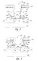
- FIG. 1is a simplified cross-sectional view of a portion of a conventional memory device prior to formation of a self-aligned contact.
- FIG. 2is a simplified cross-sectional view of a semiconductor substrate that can be processed to form a self-aligned contact in accordance with an embodiment of the present invention.
- FIG. 3is a simplified cross-sectional view of the substrate of FIG. 2 at a later point in processing, in accordance with an embodiment of the present invention.
- FIG. 4is a simplified cross-sectional view of the substrate of FIG. 3 at a later point in processing, in accordance with an embodiment of the present invention.
- FIG. 5is a simplified cross-sectional view of the substrate of FIG. 4 at a later point in processing, in accordance with an embodiment of the present invention.
- FIG. 6is a simplified cross-sectional view of the substrate of FIG. 5 at a later point in processing, in accordance with an embodiment of the present invention.
- FIG. 7is a simplified cross-sectional view of the substrate of FIG. 6 at a later point in processing, in accordance with an embodiment of the present invention.
- FIG. 8is a simplified cross-sectional view of the substrate of FIG. 7 at a later point in processing, in accordance with an embodiment of the present invention.
- Embodiments of the present inventionare directed to a self aligned contact (SAC) etch method that retains high etch selectivity while having a large process window to accommodate process variations, for example, variations in process temperature.
- SACself aligned contact
- the inventionis described with reference to a plasma etching process for etching through a selected portion of an insulating oxide layer, such as a BPSG layer, in a SAC etch used in the fabrication of memory devices.
- the inventionpertains to any applications which require selectivity to an underlying structure during the etch of doped silicon oxide dielectric layers.
- waferor “substrate” used in the following description may include any semiconductor-based structure that has an exposed silicon surface. Wafer and structure must be understood to include silicon-on insulator (SOI), silicon-on sapphire (SOS), doped and undoped semiconductors, epitaxial layers of silicon supported by a base semiconductor foundation, and other semiconductor structures.
- SOIsilicon-on insulator
- SOSsilicon-on sapphire
- doped and undoped semiconductorsepitaxial layers of silicon supported by a base semiconductor foundation, and other semiconductor structures.
- the semiconductorneed not be silicon-based.
- the semiconductorcould be silicon-germanium, germanium, or gallium arsenide.
- partis used to indicate one of several equal units of which the gaseous mixtures used in the preserit invention are comprised. Because all gases are used at identical pressures and temperatures, the term part is used instead of other terminology (e.g., moles) to underscore the importance of using the gases in particular ratios as opposed to in particular amounts.
- Embodiments of the present inventioninclude a first over-polymerizing etching step (first etching stage) for etching partially through the oxide layer of the substrate and depositing a layer of fluorocarbon polymer over exposed surfaces of the partially etched opening which results in “pinching-off” the fluorocarbon polymer layer to create an etch stop condition of the first etching step. As the fluorocarbon polymer layer pinches off in the region of the gate stacks, the first etching step stops.
- the first etching stepcan employ a first chemistry and a first set of process parameters.
- the first chemistrycan use a C x F y (x>1)-type chemistry with a very good selectivity to the silicon nitride cap and silicon nitride spacers of the gate stacks in a SAC structure.
- the first process parametersinclude a relatively low power setting (e.g., in the range of 1000-1500 W) and/or high C x F y gas flow that maintains high nitride selectivity, but also deposits enough polymer to close off the space between the gate stacks in the SAC structure and cause an etch stop condition.
- the first etching stepis used to etch the insulating oxide layer, for example BPSG layer, to a point which does not reach the top surface of an active region formed in a substrate. It will be appreciated, however, that chemistries and process parameters other than those previously described can be used as well without departing from the scope of the present invention.
- a second etching stepis employed to etch through the pinched-off polymer layer deposited during the first etching step and etch the remaining oxide layer to expose the top surface of the active region (second etching stage).
- the second etching stepcan employ a second chemistry similar to that of the first chemistry, or alternatively, a hydrogen-containing fluorocarbon chemistry.
- a second set of process parametersincludes a higher power setting than for the first set of process parameters.
- residual polymer material remaining after the first etching stepshields the nitride caps and spacers of the gate stacks while the remaining oxide is etched to expose the top surface of the active region.
- the second etching stepcompletes the SAC etch by etching down to the active region without damaging the cap and spacers of the gate stacks, and high selectivity to the nitride cap and spacers protecting the gate stack can be maintained.
- Embodiments of the present inventionallow for wider variations in process parameters than convention SAC etch processes. For example, as will be described in more detail below, a wider range of process temperatures can be used with the present invention. Thus, where performing a SAC etch at a relatively low temperature (e.g., below 30 degrees Celsius in a capacitively coupled reactor or below 20 degrees Celsius in an inductively coupled reactor) is desired, the present invention can be used. It will be appreciated, however, that embodiments of the present invention include performing a SAC etch at higher temperatures as well, such as temperatures in the range between 30-60 degrees Celsius).
- a relatively low temperaturee.g., below 30 degrees Celsius in a capacitively coupled reactor or below 20 degrees Celsius in an inductively coupled reactor
- embodiments of the present inventioninclude performing a SAC etch at higher temperatures as well, such as temperatures in the range between 30-60 degrees Celsius).
- the specific temperature values provided hereingenerally refer to the wafer temperature which may be controlled (e.g., set using the temperature setting control of an electrostatic chuck on which the wafer is positioned during processing). These values are approximate since the actual temperatures will vary depending on the particular machine being used.
- embodiments of the present inventioncan be carried out in a high density plasma (HDP) etcher, or alternatively, in a reactive ion etcher (RIE), including magnetic-enhanced reactive ion etcher (MERIE).
- HDPhigh density plasma
- RIEreactive ion etcher
- MERIEmagnetic-enhanced reactive ion etcher
- a high density plasma etcherhas both a top powered electrode and a bottom electrode, which is typically a biasable electrostatic chuck. Power is applied to both the top and bottom electrodes with separate power supplies.
- the top electrodeis typically grounded, and RF power is applied to the bottom electrode.
- any oxide etch toolincluding those having an “inductively coupled” power source or a “capacitively coupled” power source, or “dual-powered” or “dual frequency” reactors having dual-capacitively coupled power sources, can be used as well.
- etch toolsare well-known to those of ordinary skill in the art.
- An inert gassuch as argon or helium, may be added to the plasma source gas to dilute the etching gases and to enhance the uniformity of the etching process.
- a preferred diluent gasis argon. It must be understood, however that similar effects may be achieved by using other gases, such as helium, although argon is preferred.
- FIGS. 2 - 8a representative etching process according to the present invention is illustrated in FIGS. 2 - 8 . These figures show a middle portion of the structure shown in FIG. 1.
- the structure shown in FIG. 2includes a substrate 210 having a p-well 212 , which is typically doped to a predetermined conductivity, for example, p-type or n-type, depending on whether NMOS or PMOS transistors will be formed therein.
- the structureincludes conventional doped active areas 216 , and a pair of gate stacks 230 , all formed according to well-know semiconductor processing techniques.
- the gate stacks 230include an oxide layer 218 , a conductive layer 220 , such as polysilicon, nitride spacers 232 and a nitride cap 234 .
- a silicide layer 222is also typically formed between the conductive layer 220 and nitride cap 234 .
- Refractory metal suicide layer 222may comprise any refractory metal, including but not limited to, titanium, tungsten, tantalum, and molybdenum.
- the refractory metal salicide layeris substantially composed of tungsten silicide (WSi x ).
- An insulating oxide layer 224for example a borophosphosilicate glass (BPSG), borosilicate glass (BSG), or phosphosilicate glass (PSG) layer, covers the substrate 210 which contains the gate stacks 230 and active regions 216 .
- BPSGborophosphosilicate glass
- BSGborosilicate glass
- PSGphosphosilicate glass
- an antireflecting coating (ARC) 227is disposed on top of insulating oxide layer 224 .
- a photoresist material 226is deposited and patterned using conventional photolithography steps. An initial opening 235 is created in photoresist layer 226 for subsequent oxide 224 etching. The structure of FIG. 2 is then etched according to a method of the present invention.
- FIG. 3shows the structure of FIG. 2 with the contact opening 240 partially etched therein.
- the contact opening 240is etched using a directional etching process such as plasma etching.
- a first C x F y (x>1)-type chemistryis used to etch the doped insulating oxide layer 224 , with good selectivity to the silicon nitride cap 234 and spacer 232 of the gate stacks 230 .
- other fluorocarbon gasescan be used as well, such as CF x , C x H y F z (x>0), CHF 3 , CH 2 F 2 , and the like.
- the first set of process parametersincludes a relatively low power setting and relatively high gas flow of fluorocarbon gases to induce deposition of a fluorocarbon polymer layer 250 on the exposed regions of the contact opening 240 during the first etching step.
- the combination of the first chemistry and first set of process parametersresults in an over-polymerizing etch condition where the thickness of the deposited polymer layer 250 increases as the first etching step progresses. Examples of appropriate chemistries and process parameters will be provided below.
- the thickness of the polymer layer 250 in the region of the “shoulders” of the gate stacks 230begins to increase more rapidly than on the exposed vertical and horizontal surfaces of the opening 240 .
- the thickness of the polymer layer 250 at the shouldercontinues to increase, resulting in the step profile as shown in FIGS. 4 and 5.
- the polymer layer 250eventually becomes thick enough in the region of the shoulders to pinch-off the opening between the gate stacks 230 .
- an etch stop condition of the first etching stepoccurs because no more of the oxide layer can be etched, which leaves an unetched portion 260 of the insulating oxide 224 above the active region 216 .
- the phenomena producing the step profile of the polymer layer 250 and resulting etch stop conditionare well known in the art, and will not be explained in detail herein for the sake of brevity. It will be appreciated that the specific chemistry and process parameters described herein are merely provided by way of example, and that modifications made to either will not depart from the scope of the present invention.
- the plasma etching processuses a first process gas that comprises a mixture of a C x F y -type (x>1) gas and a dilute gas, such as argon.
- the C x F y -type gascan be selected from, but not limited to C 4 F 8 , C 4 F 6 , or C 5 F 8 .
- the first process gascould be a gas mixture with a flow rate of 18 sccm of C 4 F 8 and 400 sccm of Ar.
- any other gas flow rate ratiocan also be used to achieve different selectivity levels to the silicon nitride cap and spacers, as well as the deposition rate of polymer.
- Oxygen or COmay also be added to the gas mixture.
- Other gassuch as CH 2 F 2 may also be added to the C x F y gas mixture, however, as known in the art, the nitride selectivity is primarily determined by the C x F y (x>1) gas.
- the structurecan be contacted with the first plasma etch for any time sufficient to cause the deposited polymer layer 250 to pinch-off the opening between the gate stacks 30 , which leaves the unetched portion 260 above the active region 216 . It should be understood that these times may vary depending upon the substrate, the etching gas, and the physical parameters of the plasma etch.
- the first etching stepstops because of the etch stop condition in the range between below the top-of-nitride cap 234 and any distance before the etch reaches the active region 216 .
- a second plasma etch stepis performed that etches an opening through the pinched-off polymer layer 250 and removes the unetched portion 260 of the insulating oxide 224 , thereby exposing the surface of the active region 216 .
- the second chemistry of the second etching stepmay be a C x F y (x>1)-type chemistry, similar to the first chemistry of the first etching step.
- a hydrogen-containing fluorocarbon chemistrycan be used as well.
- the hydrogen-containing fluorocarbon gasis preferably selected from the group CF 4 , CHF 3 , CH 2 F 2 , C 2 HF 5 , CH 3 F, and any combinations thereof.
- An inert gassuch as argon, nitrogen, or helium, is often used in combination with the gas mixture of the second etching step.
- an appropriate gas compositionis C 4 F 8 , CH 2 F 2 , and Ar, and where a hydrogen-containing fluorocarbon chemistry is desired, CF 4 , CHF 3 , CH 2 F 2 , and Ar.
- the second process parametersincludes a relatively high power setting and a relatively low C x F y gas flow to etch through polymer layer 250 in the pinched-off region, and continue the removal of unetched portion 260 of the insulating oxide 224 , as shown in FIG. 6.
- the second etching stepfinishes the contact hole 240 etch in that the doped insulating oxide layer 224 is etched down to the active region 216 without damaging the gate stacks 230 since nitride selectivity to the nitride cap 234 and spacers 232 is maintained by the residual polymer layer 250 covering the nitride cap 234 and spacers 232 .
- the second etch steppreferably proceeds until the self-aligned contact 240 is etched through to the active region 216 in the substrate 210 , as shown in FIG. 7.
- FIG. 8illustrates the SAC opening with the patterned photoresist layers 222 , the ARC 227 , and the residual polymer layer 250 removed.
- the patterned photoresist layers 222 , the ARC 227 , and the residual polymer layer 250have been stripped using conventional methods. Such methods will typically include, but are not limited to, wet chemical stripping methods and dry plasma stripping methods.
- the process parameters discussed beloware preferably applied to wafers having a diameter of 200 mm.
- the present inventioncan be applied to wafers having smaller or larger diameters.
- Some of the particular process parameters provided in the examplemay need to be modified or scaled to apply embodiments of the present invention to wafers of different diameters, however, such modifications are still within the scope of the present invention.
- the first etchwhich may be carried out in a plasma reactor and a reactive-ion-etching (RIE) or a magnetic-enhanced reactive-ion-etching (MERIE), of the insulating layer 24 is carried out at the following conditions (the gas ratios are approximate ratios): Gases: C 4 F 8 /CH 2 F 2 /Ar 3:1:70 Pressure: 30-60 mTorr RF Power: ⁇ 1200 W Magnetic Field: 0 Gauss-100 Gauss Cathode Temperature: 10-60 Celsius Gas flows: C 4 F 8 >15 sccm CH 2 F 2 5-20 sccm Ar ⁇ 500 sccm
- the first etching stepstops when the deposited polymer layer 250 pinches-off the opening between the gate stacks 30 .
- the second etchmay be carried out in the same plasma reactor under the following conditions (the gas ratios are approximate ratios): Gases: C 4 F 8 /CH 2 F 2 /Ar 1:1:50 Pressure: 30-60 mTorr RF Power: ⁇ 1500 W Magnetic Field: 0 Gauss-100 Gauss Cathode Temperature: 10-60 Celsius Gas flows: C 4 F 8 ⁇ 15 sccm CH 2 F 2 5-20 sccm Ar >500 sccm
- This second etching stepis preferably performed until an opening is made through the deposited polymer layer 250 and the SAC opening 240 is etched to expose the active region 216 in the underlying substrate 210 .
- the second etching stepcan be alternatively performed in the same plasma reactor under the following conditions (the gas ratios are approximate ratios): Gases: CF 4 /CHF 3 /CH 2 F 2 /Ar 1:3:1:12 Pressure: 30-60 mTorr RF Power: 500-1000 W Magnetic Field: 0 Gauss-100 Gauss Cathode Temperature: 10-60 Celsius Gas flows: CF 4 10-20 sccm CHF 3 30-60 sccm CH 2 F 2 10-20 sccm Ar 100-300 sccm
- An alternative embodiment of the present inventionincludes a first etching step carried out under the following conditions (the gas ratios are approximate ratios): Gases: CF 4 /CHF 3 /CH 2 F 2 /Ar 2:4:1:100 Pressure: 30-60 mTorr RF Power: ⁇ 500 W Magnetic Field: 0 Gauss-100 Gauss Cathode Temperature: 10-60 Celsius Gas flows: CF 4 10-20 sccm CHF 3 >50 sccm CH 2 F 2 >20 sccm Ar ⁇ 200 sccm
- the conditions for the second SAC etching stepcan then be as follows (the gas ratios are approximate ratios): Gases: CF 4 /CHF 3 /CH 2 F 2 /Ar 1:3:1:12 Pressure: 30-60 mTorr RF Power: 500-1000 W Magnetic Field: 0 Gauss-100 Gauss Cathode Temperature: 10-60 Celsius Gas flows: CF 4 10-20 sccm CHF 3 30-60 sccm CH 2 F 2 10-20 sccm Ar 100-300 sccm
- the second etch stepoffers a good oxide-to-nitride selectivity while, at the same time, affords a good selectivity to undoped silicon oxide that form field oxide regions 214 .
Landscapes
- Engineering & Computer Science (AREA)
- Microelectronics & Electronic Packaging (AREA)
- Condensed Matter Physics & Semiconductors (AREA)
- General Physics & Mathematics (AREA)
- Manufacturing & Machinery (AREA)
- Computer Hardware Design (AREA)
- Physics & Mathematics (AREA)
- Power Engineering (AREA)
- Chemical & Material Sciences (AREA)
- Chemical Kinetics & Catalysis (AREA)
- General Chemical & Material Sciences (AREA)
- Inorganic Chemistry (AREA)
- Internal Circuitry In Semiconductor Integrated Circuit Devices (AREA)
- Drying Of Semiconductors (AREA)
Abstract
Description
- The present invention relates to a method for etching contacts through layers of an integrated circuit and, in particular, to a self aligned contact (SAC) etch using a multi-step process.[0001]
- The current semiconductor industry poses an ever-increasing pressure for achieving higher device density within a given die area. This is particularly true in memory circuit fabrication, for example, in the manufacture of dynamic random access memory (DRAM). Each memory cell of a DRAM typically consists of a single capacitor and a field effect transistor (FET), which is used as a charge transfer transistor. Binary data is stored as electrical charge on the capacitor in the individual memory cells. In recent years, the number and density of these memory cells on the DRAM chip has dramatically increased so that the number of memory cells on a single chip is expected to soon reach 1 Gigabit.[0002]
- The increase in circuit density is the result of scaling the individual semiconductor devices (e.g., FETs and capacitors) and increasing device packing density. The reduction in device size is due partly to the advances in photolithography and directional (anisotropic) plasma etching. The increase in device density, however, places increasing demands on many aspects of the fabrication process. For example, alignment of features from one level to the next is of critical importance, particularly the alignment of contact holes with underlying structures, such as an active area, with which they are to connect. The miniaturization of the devices makes the formation of interconnect structures difficult because maintaining sufficient electrical communication requires that the interconnect structure is formed in exact alignment with an underlying active region. At the same time, the area of the interconnect structure interfacing with the active area must be maximized. Thus, as device sizes shrink there is less room for misalignment errors of the interconnect structure.[0003]
- As the horizontal device feature sizes continue to shrink to submicrometer dimensions, it is necessary to use self-alignment techniques to relax the alignment requirements and improve critical dimension (CD) control. One such technique is called a self-aligned contact (SAC) etch, in which a pair of adjacent gates of the FETs of a pair of memory cells are utilized to align an etched opening in an insulating layer. FIG. 1 depicts a conventional memory cell construction for a DRAM at an intermediate stage of the fabrication. A pair of memory cells having respective access transistors are formed within a substrate. N-type[0004]
active regions 116 are provided in a doped p-type well 112 of substrate110 (for NMOS transistors) and the pair of access transistors haverespective gate stacks 130. Thegate stacks 130 includenitride spacers 132 andnitride caps 134 formed to protect thegate stacks 130 and provide an etch stop layer for the SAC etch. Aninsulating layer 124 of, for example, a borophosphosilicate glass (BPSG), has been applied over the substrate and transistor structures and amask layer 126 having openings for etching the insulating layer to form contact openings toactive regions 116 are also shown. - Theoretically, the[0005]
mask 126 is properly aligned to enable a SAC etch of theinsulating layer 124 to provide contact openings down to theactive regions 116. - The SAC etch processes primarily involve dry etches or plasma etches. Almost all of the current dry etch technology for SAC etch processes uses a C[0006]xFy(x>1)-type plasma chemistry, such as, for example, C4F8, C5F8, or C4F6, in combination with other diluent gases. The CxFytype chemistry is favored because it offers very high selectivity to the silicon nitride cap and silicon nitride spacers, which are the most typical etch stop material for gate stack protection in a SAC etch. However, it has the disadvantage that the conventional SAC etch parameters have a very small process window. This is primarily due to the fact that the CxFy-type chemistry generates a fluorocarbon polymer which is more carbon rich than the polymers generated with other types of chemistry. With this very carbon-rich fluorocarbon polymer, the etch often results in etch stop condition, a situation when etching stops before reaching the substrate, when the gas flow or temperature is off even by a small amount from the optimal setting.
- Conventional approaches to this issue generally attempt to minimize the deposition of polymer, while still maintaining the etch selectivity and controlling overetching conditions to ensure completion of the SAC etch. That is, conventional SAC etch processes try to balance etch chemistry and etch conditions to thoroughly etch through the BPSG, but does not etch the[0007]
silicon nitride spacers 132 andcaps 134 of thegate stacks 130, and does not deposit enough polymer to cause an etch stop condition prior to exposing the active region. This has been accomplished by varying the chemistry and process parameters, such as the gas phase chemistry through adjustments in the plasma reactor gases or the operating pressure. However, as previously mentioned, to perform an adequate SAC etch using conventional methods, the process parameters must be maintained within a very narrow range. Therefore, there is a need for an alternative etching process that can maintain selectivity to nitride regions while allowing for variations in process parameters. - The present invention is directed to a method for forming an opening through an interlayer to expose an underlying surface that retains high etch selectivity while having a relatively large process window to accommodate process variations. The method includes masking an interlayer to define an etching area at which the opening is formed, etching the interlayer under a first etching condition through the etching area, and forming a protective layer over portions of exposed surfaces of the opening during etching under the first etching condition. The formation of the protective layer can be performed by utilizing an over-polymerizing etch condition that promotes the formation of a fluorocarbon polymer layer.[0008]
- The formation of the protective layer continues until an etch stop condition via polymer pinch-off is produced, shutting off etching of the interlayer under the first condition prior to exposing the underlying surface. The method continues with etching through the protective layer under a second etching condition to expose a residual interlayer, and etching the exposed residual interlayer under the second etching condition to expose the underlying surface. The protective layer deposited prior to etching under the second condition shields any underlying structures, resulting in high etch selectivity during the second etch.[0009]
- FIG. 1 is a simplified cross-sectional view of a portion of a conventional memory device prior to formation of a self-aligned contact.[0010]
- FIG. 2 is a simplified cross-sectional view of a semiconductor substrate that can be processed to form a self-aligned contact in accordance with an embodiment of the present invention.[0011]
- FIG. 3 is a simplified cross-sectional view of the substrate of FIG. 2 at a later point in processing, in accordance with an embodiment of the present invention.[0012]
- FIG. 4 is a simplified cross-sectional view of the substrate of FIG. 3 at a later point in processing, in accordance with an embodiment of the present invention.[0013]
- FIG. 5 is a simplified cross-sectional view of the substrate of FIG. 4 at a later point in processing, in accordance with an embodiment of the present invention.[0014]
- FIG. 6 is a simplified cross-sectional view of the substrate of FIG. 5 at a later point in processing, in accordance with an embodiment of the present invention.[0015]
- FIG. 7 is a simplified cross-sectional view of the substrate of FIG. 6 at a later point in processing, in accordance with an embodiment of the present invention.[0016]
- FIG. 8 is a simplified cross-sectional view of the substrate of FIG. 7 at a later point in processing, in accordance with an embodiment of the present invention.[0017]
- Embodiments of the present invention are directed to a self aligned contact (SAC) etch method that retains high etch selectivity while having a large process window to accommodate process variations, for example, variations in process temperature. In the discussion which follows, the invention is described with reference to a plasma etching process for etching through a selected portion of an insulating oxide layer, such as a BPSG layer, in a SAC etch used in the fabrication of memory devices. However, it should be understood that the invention pertains to any applications which require selectivity to an underlying structure during the etch of doped silicon oxide dielectric layers. Additionally, in the following detailed description, reference is made to various specific embodiments in which the invention may be practiced. These embodiments are described with sufficient detail to enable those skilled in the art to practice the invention, and it is to be understood that other embodiments may be employed, and that structural and process changes may be made without departing from the teachings of the invention.[0018]
- It will be appreciated that the terms “wafer” or “substrate” used in the following description may include any semiconductor-based structure that has an exposed silicon surface. Wafer and structure must be understood to include silicon-on insulator (SOI), silicon-on sapphire (SOS), doped and undoped semiconductors, epitaxial layers of silicon supported by a base semiconductor foundation, and other semiconductor structures. The semiconductor need not be silicon-based. The semiconductor could be silicon-germanium, germanium, or gallium arsenide. When reference is made to a wafer or substrate in the following description, previous process steps may have been utilized to form regions or junctions or layers in or on the base semiconductor or foundation.[0019]
- Additionally, the term “part” is used to indicate one of several equal units of which the gaseous mixtures used in the preserit invention are comprised. Because all gases are used at identical pressures and temperatures, the term part is used instead of other terminology (e.g., moles) to underscore the importance of using the gases in particular ratios as opposed to in particular amounts.[0020]
- Embodiments of the present invention include a first over-polymerizing etching step (first etching stage) for etching partially through the oxide layer of the substrate and depositing a layer of fluorocarbon polymer over exposed surfaces of the partially etched opening which results in “pinching-off” the fluorocarbon polymer layer to create an etch stop condition of the first etching step. As the fluorocarbon polymer layer pinches off in the region of the gate stacks, the first etching step stops. The first etching step can employ a first chemistry and a first set of process parameters. For example, the first chemistry can use a C[0021]xFy(x>1)-type chemistry with a very good selectivity to the silicon nitride cap and silicon nitride spacers of the gate stacks in a SAC structure. The first process parameters include a relatively low power setting (e.g., in the range of 1000-1500 W) and/or high CxFygas flow that maintains high nitride selectivity, but also deposits enough polymer to close off the space between the gate stacks in the SAC structure and cause an etch stop condition. The first etching step is used to etch the insulating oxide layer, for example BPSG layer, to a point which does not reach the top surface of an active region formed in a substrate. It will be appreciated, however, that chemistries and process parameters other than those previously described can be used as well without departing from the scope of the present invention.
- A second etching step is employed to etch through the pinched-off polymer layer deposited during the first etching step and etch the remaining oxide layer to expose the top surface of the active region (second etching stage). The second etching step can employ a second chemistry similar to that of the first chemistry, or alternatively, a hydrogen-containing fluorocarbon chemistry. A second set of process parameters includes a higher power setting than for the first set of process parameters. During the second etching step, residual polymer material remaining after the first etching step shields the nitride caps and spacers of the gate stacks while the remaining oxide is etched to expose the top surface of the active region. As a result, the second etching step completes the SAC etch by etching down to the active region without damaging the cap and spacers of the gate stacks, and high selectivity to the nitride cap and spacers protecting the gate stack can be maintained.[0022]
- Embodiments of the present invention allow for wider variations in process parameters than convention SAC etch processes. For example, as will be described in more detail below, a wider range of process temperatures can be used with the present invention. Thus, where performing a SAC etch at a relatively low temperature (e.g., below 30 degrees Celsius in a capacitively coupled reactor or below 20 degrees Celsius in an inductively coupled reactor) is desired, the present invention can be used. It will be appreciated, however, that embodiments of the present invention include performing a SAC etch at higher temperatures as well, such as temperatures in the range between 30-60 degrees Celsius). It will be further appreciated that the specific temperature values provided herein generally refer to the wafer temperature which may be controlled (e.g., set using the temperature setting control of an electrostatic chuck on which the wafer is positioned during processing). These values are approximate since the actual temperatures will vary depending on the particular machine being used.[0023]
- Moreover, embodiments of the present invention can be carried out in a high density plasma (HDP) etcher, or alternatively, in a reactive ion etcher (RIE), including magnetic-enhanced reactive ion etcher (MERIE). As is well known, a high density plasma etcher has both a top powered electrode and a bottom electrode, which is typically a biasable electrostatic chuck. Power is applied to both the top and bottom electrodes with separate power supplies. In a reactive ion etcher, the top electrode is typically grounded, and RF power is applied to the bottom electrode. More generally, any oxide etch tool, including those having an “inductively coupled” power source or a “capacitively coupled” power source, or “dual-powered” or “dual frequency” reactors having dual-capacitively coupled power sources, can be used as well. These various types of etch tools are well-known to those of ordinary skill in the art.[0024]
- An inert gas, such as argon or helium, may be added to the plasma source gas to dilute the etching gases and to enhance the uniformity of the etching process. A preferred diluent gas is argon. It must be understood, however that similar effects may be achieved by using other gases, such as helium, although argon is preferred.[0025]
- Referring now to the drawings, where like elements are designated by like reference numerals, a representative etching process according to the present invention is illustrated in FIGS.[0026]2-8. These figures show a middle portion of the structure shown in FIG. 1.
- The structure shown in FIG. 2 includes a[0027]
substrate 210 having a p-well212, which is typically doped to a predetermined conductivity, for example, p-type or n-type, depending on whether NMOS or PMOS transistors will be formed therein. The structure includes conventional dopedactive areas 216, and a pair of gate stacks230, all formed according to well-know semiconductor processing techniques. The gate stacks230 include anoxide layer 218, aconductive layer 220, such as polysilicon,nitride spacers 232 and anitride cap 234. It will be appreciated that an oxide material can be substituted for the nitride material of the nitride spacers andcap silicide layer 222 is also typically formed between theconductive layer 220 andnitride cap 234. Refractorymetal suicide layer 222 may comprise any refractory metal, including but not limited to, titanium, tungsten, tantalum, and molybdenum. Preferably, the refractory metal salicide layer is substantially composed of tungsten silicide (WSix). An insulatingoxide layer 224, for example a borophosphosilicate glass (BPSG), borosilicate glass (BSG), or phosphosilicate glass (PSG) layer, covers thesubstrate 210 which contains the gate stacks230 andactive regions 216. Optionally, an antireflecting coating (ARC)227 is disposed on top of insulatingoxide layer 224. - To create a[0028]
contact opening 240 intosemiconductor substrate 210 throughoxide layer 224, aphotoresist material 226 is deposited and patterned using conventional photolithography steps. Aninitial opening 235 is created inphotoresist layer 226 forsubsequent oxide 224 etching. The structure of FIG. 2 is then etched according to a method of the present invention. - Reference is now made to FIG. 3, which shows the structure of FIG. 2 with the[0029]
contact opening 240 partially etched therein. Thecontact opening 240 is etched using a directional etching process such as plasma etching. In the present embodiment, a first CxFy(x>1)-type chemistry is used to etch the doped insulatingoxide layer 224, with good selectivity to thesilicon nitride cap 234 andspacer 232 of the gate stacks230. However, in alternative embodiments of the present invention, other fluorocarbon gases can be used as well, such as CFx, CxHyFz(x>0), CHF3, CH2F2, and the like. As previously mentioned, the first set of process parameters includes a relatively low power setting and relatively high gas flow of fluorocarbon gases to induce deposition of afluorocarbon polymer layer 250 on the exposed regions of thecontact opening 240 during the first etching step. The combination of the first chemistry and first set of process parameters results in an over-polymerizing etch condition where the thickness of the depositedpolymer layer 250 increases as the first etching step progresses. Examples of appropriate chemistries and process parameters will be provided below. - As illustrated in FIG. 4, as the first etching step reaches a depth that begins to expose portions of the[0030]
nitride cap 234 andspacers 232 of the gate stacks230, the thickness of thepolymer layer 250 in the region of the “shoulders” of the gate stacks230 begins to increase more rapidly than on the exposed vertical and horizontal surfaces of theopening 240. As the first etching process continues, the thickness of thepolymer layer 250 at the shoulder continues to increase, resulting in the step profile as shown in FIGS. 4 and 5. As shown in FIG. 5, thepolymer layer 250 eventually becomes thick enough in the region of the shoulders to pinch-off the opening between the gate stacks230. As a result, an etch stop condition of the first etching step occurs because no more of the oxide layer can be etched, which leaves anunetched portion 260 of the insulatingoxide 224 above theactive region 216. The phenomena producing the step profile of thepolymer layer 250 and resulting etch stop condition are well known in the art, and will not be explained in detail herein for the sake of brevity. It will be appreciated that the specific chemistry and process parameters described herein are merely provided by way of example, and that modifications made to either will not depart from the scope of the present invention. - The plasma etching process uses a first process gas that comprises a mixture of a C[0031]xFy-type (x>1) gas and a dilute gas, such as argon. The CxFy-type gas can be selected from, but not limited to C4F8, C4F6, or C5F8. For example, the first process gas could be a gas mixture with a flow rate of18 sccm of C4F8and 400 sccm of Ar. However, any other gas flow rate ratio can also be used to achieve different selectivity levels to the silicon nitride cap and spacers, as well as the deposition rate of polymer. Oxygen or CO may also be added to the gas mixture. Other gas such as CH2F2may also be added to the CxFygas mixture, however, as known in the art, the nitride selectivity is primarily determined by the CxFy(x>1) gas.
- The structure can be contacted with the first plasma etch for any time sufficient to cause the deposited[0032]
polymer layer 250 to pinch-off the opening between the gate stacks30, which leaves theunetched portion 260 above theactive region 216. It should be understood that these times may vary depending upon the substrate, the etching gas, and the physical parameters of the plasma etch. Preferably, the first etching step stops because of the etch stop condition in the range between below the top-of-nitride cap 234 and any distance before the etch reaches theactive region 216. - Following the first etching step, a second plasma etch step is performed that etches an opening through the pinched-off[0033]
polymer layer 250 and removes theunetched portion 260 of the insulatingoxide 224, thereby exposing the surface of theactive region 216. The second chemistry of the second etching step may be a CxFy(x>1)-type chemistry, similar to the first chemistry of the first etching step. Alternatively, a hydrogen-containing fluorocarbon chemistry can be used as well. Where a hydrogen-containing fluorocarbon chemistry is used, the hydrogen-containing fluorocarbon gas is preferably selected from the group CF4, CHF3, CH2F2, C2HF5, CH3F, and any combinations thereof. An inert gas, such as argon, nitrogen, or helium, is often used in combination with the gas mixture of the second etching step. For example, an appropriate gas composition is C4F8, CH2F2, and Ar, and where a hydrogen-containing fluorocarbon chemistry is desired, CF4, CHF3, CH2F2, and Ar. - As previously mentioned, if C[0034]xFytype chemistry is used in the second etching step, the second process parameters includes a relatively high power setting and a relatively low CxFygas flow to etch through
polymer layer 250 in the pinched-off region, and continue the removal ofunetched portion 260 of the insulatingoxide 224, as shown in FIG. 6. The second etching step finishes thecontact hole 240 etch in that the doped insulatingoxide layer 224 is etched down to theactive region 216 without damaging the gate stacks230 since nitride selectivity to thenitride cap 234 andspacers 232 is maintained by theresidual polymer layer 250 covering thenitride cap 234 andspacers 232. The second etch step preferably proceeds until the self-alignedcontact 240 is etched through to theactive region 216 in thesubstrate 210, as shown in FIG. 7. - FIG. 8 illustrates the SAC opening with the patterned photoresist layers[0035]222, the
ARC 227, and theresidual polymer layer 250 removed. The patterned photoresist layers222, theARC 227, and theresidual polymer layer 250 have been stripped using conventional methods. Such methods will typically include, but are not limited to, wet chemical stripping methods and dry plasma stripping methods. - The invention is further explained with reference to the following examples. The examples are also described with reference to FIGS.[0036]2-8. The following examples are provided merely to assist in describing the present invention by providing specific embodiments. However, the present invention is not intended to be limited by the particular examples described below. Additionally, it will be appreciated that the process parameters described in the present example can be adjusted based on a variety of factors, including device geometry, type of processing tools, and the like. For example, embodiments of the present invention allow for process temperatures below 40 degrees Celsius for capacitively coupled reactors and below 20 degrees Celsius for inductively coupled reactors. The parameters in the present example may also be adjusted or scaled to accommodate wafers of different diameters. For example, the process parameters discussed below are preferably applied to wafers having a diameter of 200 mm. However, it will be appreciated by those of ordinary skill in the art that the present invention can be applied to wafers having smaller or larger diameters. Some of the particular process parameters provided in the example may need to be modified or scaled to apply embodiments of the present invention to wafers of different diameters, however, such modifications are still within the scope of the present invention.
- The first etch, which may be carried out in a plasma reactor and a reactive-ion-etching (RIE) or a magnetic-enhanced reactive-ion-etching (MERIE), of the insulating layer[0037]24 is carried out at the following conditions (the gas ratios are approximate ratios):
Gases: C4F8/CH2F2/Ar 3:1:70 Pressure: 30-60 mTorr RF Power: ≦1200 W Magnetic Field: 0 Gauss-100 Gauss Cathode Temperature: 10-60 Celsius Gas flows: C4F8>15 sccm CH2F25-20 sccm Ar <500 sccm - As noted, the first etching step stops when the deposited[0038]
polymer layer 250 pinches-off the opening between the gate stacks30. - The second etch may be carried out in the same plasma reactor under the following conditions (the gas ratios are approximate ratios):[0039]
Gases: C4F8/CH2F2/Ar 1:1:50 Pressure: 30-60 mTorr RF Power: ≧1500 W Magnetic Field: 0 Gauss-100 Gauss Cathode Temperature: 10-60 Celsius Gas flows: C4F8<15 sccm CH2F25-20 sccm Ar >500 sccm - This second etching step is preferably performed until an opening is made through the deposited[0040]
polymer layer 250 and the SAC opening240 is etched to expose theactive region 216 in theunderlying substrate 210. - The second etching step can be alternatively performed in the same plasma reactor under the following conditions (the gas ratios are approximate ratios):[0041]
Gases: CF4/CHF3/CH2F2/Ar 1:3:1:12 Pressure: 30-60 mTorr RF Power: 500-1000 W Magnetic Field: 0 Gauss-100 Gauss Cathode Temperature: 10-60 Celsius Gas flows: CF410-20 sccm CHF330-60 sccm CH2F210-20 sccm Ar 100-300 sccm - An alternative embodiment of the present invention includes a first etching step carried out under the following conditions (the gas ratios are approximate ratios):[0042]
Gases: CF4/CHF3/CH2F2/Ar 2:4:1:100 Pressure: 30-60 mTorr RF Power: <500 W Magnetic Field: 0 Gauss-100 Gauss Cathode Temperature: 10-60 Celsius Gas flows: CF410-20 sccm CHF3>50 sccm CH2F2>20 sccm Ar <200 sccm - The conditions for the second SAC etching step can then be as follows (the gas ratios are approximate ratios):[0043]
Gases: CF4/CHF3/CH2F2/Ar 1:3:1:12 Pressure: 30-60 mTorr RF Power: 500-1000 W Magnetic Field: 0 Gauss-100 Gauss Cathode Temperature: 10-60 Celsius Gas flows: CF410-20 sccm CHF330-60 sccm CH2F210-20 sccm Ar 100-300 sccm - The second etch step offers a good oxide-to-nitride selectivity while, at the same time, affords a good selectivity to undoped silicon oxide that form field oxide regions[0044]214.
- The above description illustrates preferred embodiments which achieve the features and advantages of the present invention. It is not intended that the present invention be limited to the illustrated embodiments. Modifications and substitutions to specific process conditions and structures can be made without departing from the spirit and scope of the present invention. Accordingly, the invention is not to be considered as being limited by the foregoing description and drawings, but is only limited by the scope of the appended claims.[0045]
Claims (92)
Priority Applications (1)
| Application Number | Priority Date | Filing Date | Title |
|---|---|---|---|
| US10/226,488US6716766B2 (en) | 2002-08-22 | 2002-08-22 | Process variation resistant self aligned contact etch |
Applications Claiming Priority (1)
| Application Number | Priority Date | Filing Date | Title |
|---|---|---|---|
| US10/226,488US6716766B2 (en) | 2002-08-22 | 2002-08-22 | Process variation resistant self aligned contact etch |
Publications (2)
| Publication Number | Publication Date |
|---|---|
| US20040038546A1true US20040038546A1 (en) | 2004-02-26 |
| US6716766B2 US6716766B2 (en) | 2004-04-06 |
Family
ID=31887242
Family Applications (1)
| Application Number | Title | Priority Date | Filing Date |
|---|---|---|---|
| US10/226,488Expired - LifetimeUS6716766B2 (en) | 2002-08-22 | 2002-08-22 | Process variation resistant self aligned contact etch |
Country Status (1)
| Country | Link |
|---|---|
| US (1) | US6716766B2 (en) |
Cited By (18)
| Publication number | Priority date | Publication date | Assignee | Title |
|---|---|---|---|---|
| US20040157459A1 (en)* | 2003-02-11 | 2004-08-12 | Applied Materials, Inc. | Method of etching ferroelectric layers |
| US7037774B1 (en)* | 2004-10-21 | 2006-05-02 | Integrated Device Technology, Inc. | Self-aligned contact structure and process for forming self-aligned contact structure |
| US7074722B2 (en)* | 2003-10-23 | 2006-07-11 | Hynix Semiconductor Inc. | Method for fabricating semiconductor device with fine pattern |
| US20060240654A1 (en)* | 2005-04-22 | 2006-10-26 | Macronix International Co., Ltd. | Process of forming a self-aligned contact in a semiconductor device |
| US20080081429A1 (en)* | 2006-09-29 | 2008-04-03 | Hynix Semiconductor Inc. | Method for fabricating capacitor in semiconductor device |
| US20090087978A1 (en)* | 2007-10-01 | 2009-04-02 | Nanya Technology Corporation | Interconnect manufacturing process |
| US8664012B2 (en) | 2011-09-30 | 2014-03-04 | Tokyo Electron Limited | Combined silicon oxide etch and contamination removal process |
| EP2991103A1 (en)* | 2014-08-28 | 2016-03-02 | Tokyo Electron Limited | Etching method |
| EP3046139A1 (en)* | 2015-01-16 | 2016-07-20 | Tokyo Electron Limited | Etching method |
| EP3046138A1 (en)* | 2015-01-16 | 2016-07-20 | Tokyo Electron Limited | Etching method |
| KR20160088816A (en)* | 2015-01-16 | 2016-07-26 | 도쿄엘렉트론가부시키가이샤 | Etching method |
| CN105914144A (en)* | 2015-02-24 | 2016-08-31 | 东京毅力科创株式会社 | Etching method |
| KR20170000791A (en)* | 2015-06-24 | 2017-01-03 | 도쿄엘렉트론가부시키가이샤 | Etching method |
| EP3229264A1 (en)* | 2016-04-07 | 2017-10-11 | Semiconductor Manufacturing International Corporation (Shanghai) | Etching method and fabrication method of semiconductor structures |
| US20180308753A1 (en)* | 2017-04-19 | 2018-10-25 | Tokyo Electron Limited | Process Integration Techniques Using A Carbon Layer To Form Self-Aligned Structures |
| US10340142B1 (en)* | 2018-03-12 | 2019-07-02 | Globalfoundries Inc. | Methods, apparatus and system for self-aligned metal hard masks |
| US10784158B2 (en) | 2018-05-17 | 2020-09-22 | Imec Vzw | Area-selective deposition of a tantalum silicide TaSix mask material |
| CN114930508A (en)* | 2020-05-22 | 2022-08-19 | 应用材料公司 | Directional selective junction cleaning with field polymer protection |
Families Citing this family (5)
| Publication number | Priority date | Publication date | Assignee | Title |
|---|---|---|---|---|
| JP3759895B2 (en)* | 2001-10-24 | 2006-03-29 | 松下電器産業株式会社 | Etching method |
| KR100505443B1 (en)* | 2002-12-26 | 2005-08-04 | 주식회사 하이닉스반도체 | Method for fabricating semiconductor device |
| US20070066047A1 (en)* | 2005-09-18 | 2007-03-22 | Jianhui Ye | Method of forming opening and contact |
| US8847291B2 (en)* | 2012-11-02 | 2014-09-30 | Atmel Corporation | Stress relief for plastic encapsulated devices |
| JP6592400B2 (en)* | 2016-05-19 | 2019-10-16 | 東京エレクトロン株式会社 | Etching method |
Citations (5)
| Publication number | Priority date | Publication date | Assignee | Title |
|---|---|---|---|---|
| US5817579A (en)* | 1997-04-09 | 1998-10-06 | Vanguard International Semiconductor Corporation | Two step plasma etch method for forming self aligned contact |
| US6028001A (en)* | 1998-04-02 | 2000-02-22 | Samsung Electronics Co., Ltd. | Methods of fabricating contact holes for integrated circuit substrates by etching to define a sidewall and concurrently forming a polymer on the sidewall |
| US6191042B1 (en)* | 1998-12-15 | 2001-02-20 | United Microelectronics Corp. | Method of forming node contact opening |
| US6326312B1 (en)* | 1997-12-30 | 2001-12-04 | Lg Semicon Co., Ltd. | Contact hole of semiconductor and its forming method |
| US6372634B1 (en)* | 1999-06-15 | 2002-04-16 | Cypress Semiconductor Corp. | Plasma etch chemistry and method of improving etch control |
Family Cites Families (2)
| Publication number | Priority date | Publication date | Assignee | Title |
|---|---|---|---|---|
| US5948701A (en) | 1997-07-30 | 1999-09-07 | Chartered Semiconductor Manufacturing, Ltd. | Self-aligned contact (SAC) etching using polymer-building chemistry |
| US6337285B1 (en) | 2000-03-21 | 2002-01-08 | Micron Technology, Inc. | Self-aligned contact (SAC) etch with dual-chemistry process |
- 2002
- 2002-08-22USUS10/226,488patent/US6716766B2/ennot_activeExpired - Lifetime
Patent Citations (5)
| Publication number | Priority date | Publication date | Assignee | Title |
|---|---|---|---|---|
| US5817579A (en)* | 1997-04-09 | 1998-10-06 | Vanguard International Semiconductor Corporation | Two step plasma etch method for forming self aligned contact |
| US6326312B1 (en)* | 1997-12-30 | 2001-12-04 | Lg Semicon Co., Ltd. | Contact hole of semiconductor and its forming method |
| US6028001A (en)* | 1998-04-02 | 2000-02-22 | Samsung Electronics Co., Ltd. | Methods of fabricating contact holes for integrated circuit substrates by etching to define a sidewall and concurrently forming a polymer on the sidewall |
| US6191042B1 (en)* | 1998-12-15 | 2001-02-20 | United Microelectronics Corp. | Method of forming node contact opening |
| US6372634B1 (en)* | 1999-06-15 | 2002-04-16 | Cypress Semiconductor Corp. | Plasma etch chemistry and method of improving etch control |
Cited By (34)
| Publication number | Priority date | Publication date | Assignee | Title |
|---|---|---|---|---|
| US20040157459A1 (en)* | 2003-02-11 | 2004-08-12 | Applied Materials, Inc. | Method of etching ferroelectric layers |
| US6943039B2 (en)* | 2003-02-11 | 2005-09-13 | Applied Materials Inc. | Method of etching ferroelectric layers |
| US7074722B2 (en)* | 2003-10-23 | 2006-07-11 | Hynix Semiconductor Inc. | Method for fabricating semiconductor device with fine pattern |
| US7037774B1 (en)* | 2004-10-21 | 2006-05-02 | Integrated Device Technology, Inc. | Self-aligned contact structure and process for forming self-aligned contact structure |
| US7723229B2 (en)* | 2005-04-22 | 2010-05-25 | Macronix International Co., Ltd. | Process of forming a self-aligned contact in a semiconductor device |
| US20060240654A1 (en)* | 2005-04-22 | 2006-10-26 | Macronix International Co., Ltd. | Process of forming a self-aligned contact in a semiconductor device |
| US20080081429A1 (en)* | 2006-09-29 | 2008-04-03 | Hynix Semiconductor Inc. | Method for fabricating capacitor in semiconductor device |
| US7723239B2 (en)* | 2006-09-29 | 2010-05-25 | Hynix Semiconductor Inc | Method for fabricating capacitor in semiconductor device |
| US20090087978A1 (en)* | 2007-10-01 | 2009-04-02 | Nanya Technology Corporation | Interconnect manufacturing process |
| US8664012B2 (en) | 2011-09-30 | 2014-03-04 | Tokyo Electron Limited | Combined silicon oxide etch and contamination removal process |
| KR20160028370A (en)* | 2014-08-28 | 2016-03-11 | 도쿄엘렉트론가부시키가이샤 | Etching method |
| EP2991103A1 (en)* | 2014-08-28 | 2016-03-02 | Tokyo Electron Limited | Etching method |
| KR102361782B1 (en) | 2014-08-28 | 2022-02-10 | 도쿄엘렉트론가부시키가이샤 | Etching method |
| EP3046139A1 (en)* | 2015-01-16 | 2016-07-20 | Tokyo Electron Limited | Etching method |
| EP3046138A1 (en)* | 2015-01-16 | 2016-07-20 | Tokyo Electron Limited | Etching method |
| KR20160088816A (en)* | 2015-01-16 | 2016-07-26 | 도쿄엘렉트론가부시키가이샤 | Etching method |
| KR20160088819A (en)* | 2015-01-16 | 2016-07-26 | 도쿄엘렉트론가부시키가이샤 | Etching method |
| KR102513051B1 (en)* | 2015-01-16 | 2023-03-22 | 도쿄엘렉트론가부시키가이샤 | Etching method |
| KR102458996B1 (en)* | 2015-01-16 | 2022-10-25 | 도쿄엘렉트론가부시키가이샤 | Etching method |
| CN105914144A (en)* | 2015-02-24 | 2016-08-31 | 东京毅力科创株式会社 | Etching method |
| US20180190505A1 (en)* | 2015-02-24 | 2018-07-05 | Tokyo Electron Limited | Method of selectively etching silicon oxide film on substrate |
| KR20160103531A (en)* | 2015-02-24 | 2016-09-01 | 도쿄엘렉트론가부시키가이샤 | Etching method |
| US11205577B2 (en)* | 2015-02-24 | 2021-12-21 | Tokyo Electron Limited | Method of selectively etching silicon oxide film on substrate |
| KR102363778B1 (en)* | 2015-02-24 | 2022-02-15 | 도쿄엘렉트론가부시키가이샤 | Etching method |
| KR20170000791A (en)* | 2015-06-24 | 2017-01-03 | 도쿄엘렉트론가부시키가이샤 | Etching method |
| KR102494293B1 (en) | 2015-06-24 | 2023-01-31 | 도쿄엘렉트론가부시키가이샤 | Etching method |
| CN107275202A (en)* | 2016-04-07 | 2017-10-20 | 中芯国际集成电路制造(上海)有限公司 | The forming method of lithographic method and semiconductor structure |
| US10573551B2 (en) | 2016-04-07 | 2020-02-25 | Semiconductor Manufacturing International (Shanghai) Corporation | Etching method and fabrication method of semiconductor structures |
| EP3229264A1 (en)* | 2016-04-07 | 2017-10-11 | Semiconductor Manufacturing International Corporation (Shanghai) | Etching method and fabrication method of semiconductor structures |
| US20180308753A1 (en)* | 2017-04-19 | 2018-10-25 | Tokyo Electron Limited | Process Integration Techniques Using A Carbon Layer To Form Self-Aligned Structures |
| US10600687B2 (en)* | 2017-04-19 | 2020-03-24 | Tokyo Electron Limited | Process integration techniques using a carbon layer to form self-aligned structures |
| US10340142B1 (en)* | 2018-03-12 | 2019-07-02 | Globalfoundries Inc. | Methods, apparatus and system for self-aligned metal hard masks |
| US10784158B2 (en) | 2018-05-17 | 2020-09-22 | Imec Vzw | Area-selective deposition of a tantalum silicide TaSix mask material |
| CN114930508A (en)* | 2020-05-22 | 2022-08-19 | 应用材料公司 | Directional selective junction cleaning with field polymer protection |
Also Published As
| Publication number | Publication date |
|---|---|
| US6716766B2 (en) | 2004-04-06 |
Similar Documents
| Publication | Publication Date | Title |
|---|---|---|
| US6716766B2 (en) | Process variation resistant self aligned contact etch | |
| US6337285B1 (en) | Self-aligned contact (SAC) etch with dual-chemistry process | |
| US7541270B2 (en) | Methods for forming openings in doped silicon dioxide | |
| US7265050B2 (en) | Methods for fabricating memory devices using sacrificial layers | |
| US6362073B2 (en) | Method for forming semiconductor device having low parasite capacitance using air gap and self-aligned contact plug | |
| US6803318B1 (en) | Method of forming self aligned contacts | |
| US5935877A (en) | Etch process for forming contacts over titanium silicide | |
| US7470628B2 (en) | Etching methods | |
| KR20020044908A (en) | Methods of fabricating a semiconductor device using an anti-reflective layer and a self-aligned contact technique and semiconductor devices fabricated thereby | |
| US6372638B1 (en) | Method for forming a conductive plug between conductive layers of an integrated circuit | |
| US7109085B2 (en) | Etching process to avoid polysilicon notching | |
| US6227211B1 (en) | Uniformity improvement of high aspect ratio contact by stop layer | |
| KR100512904B1 (en) | Fabricating method for semiconductor device | |
| US6239011B1 (en) | Method of self-aligned contact hole etching by fluorine-containing discharges | |
| KR100626928B1 (en) | How to form a silicide gate stack for self-matching contact etching | |
| US6236091B1 (en) | Method of forming a local interconnect with improved etch selectivity of silicon dioxide/silicide | |
| US20010034136A1 (en) | Method for improving contact resistance of silicide layer in a semiconductor device | |
| US20070284743A1 (en) | Fabricating Memory Devices Using Sacrificial Layers and Memory Devices Fabricated by Same | |
| KR20020060461A (en) | A method for forming gate spacer of self-aligned contact | |
| US20020119618A1 (en) | Method for forming contacts of memory devices using an etch stop layer | |
| KR100835506B1 (en) | Manufacturing method of semiconductor device | |
| KR100520140B1 (en) | Method for forming capacitor of semiconductor device | |
| KR100431818B1 (en) | Forming method for self aligned contact of semiconductor device | |
| KR100333127B1 (en) | Capacitor Manufacturing Method for Semiconductor Devices | |
| KR20030001178A (en) | Method for forming plug in semiconductor device |
Legal Events
| Date | Code | Title | Description |
|---|---|---|---|
| AS | Assignment | Owner name:MICRON TECHNOLOGY, INC., IDAHO Free format text:ASSIGNMENT OF ASSIGNORS INTEREST;ASSIGNOR:KO, KEI-YU;REEL/FRAME:013236/0503 Effective date:20020807 | |
| FEPP | Fee payment procedure | Free format text:PAYOR NUMBER ASSIGNED (ORIGINAL EVENT CODE: ASPN); ENTITY STATUS OF PATENT OWNER: LARGE ENTITY | |
| STCF | Information on status: patent grant | Free format text:PATENTED CASE | |
| CC | Certificate of correction | ||
| FPAY | Fee payment | Year of fee payment:4 | |
| FPAY | Fee payment | Year of fee payment:8 | |
| FPAY | Fee payment | Year of fee payment:12 | |
| AS | Assignment | Owner name:U.S. BANK NATIONAL ASSOCIATION, AS COLLATERAL AGENT, CALIFORNIA Free format text:SECURITY INTEREST;ASSIGNOR:MICRON TECHNOLOGY, INC.;REEL/FRAME:038669/0001 Effective date:20160426 Owner name:U.S. BANK NATIONAL ASSOCIATION, AS COLLATERAL AGEN Free format text:SECURITY INTEREST;ASSIGNOR:MICRON TECHNOLOGY, INC.;REEL/FRAME:038669/0001 Effective date:20160426 | |
| AS | Assignment | Owner name:MORGAN STANLEY SENIOR FUNDING, INC., AS COLLATERAL AGENT, MARYLAND Free format text:PATENT SECURITY AGREEMENT;ASSIGNOR:MICRON TECHNOLOGY, INC.;REEL/FRAME:038954/0001 Effective date:20160426 Owner name:MORGAN STANLEY SENIOR FUNDING, INC., AS COLLATERAL Free format text:PATENT SECURITY AGREEMENT;ASSIGNOR:MICRON TECHNOLOGY, INC.;REEL/FRAME:038954/0001 Effective date:20160426 | |
| AS | Assignment | Owner name:U.S. BANK NATIONAL ASSOCIATION, AS COLLATERAL AGENT, CALIFORNIA Free format text:CORRECTIVE ASSIGNMENT TO CORRECT THE REPLACE ERRONEOUSLY FILED PATENT #7358718 WITH THE CORRECT PATENT #7358178 PREVIOUSLY RECORDED ON REEL 038669 FRAME 0001. ASSIGNOR(S) HEREBY CONFIRMS THE SECURITY INTEREST;ASSIGNOR:MICRON TECHNOLOGY, INC.;REEL/FRAME:043079/0001 Effective date:20160426 Owner name:U.S. BANK NATIONAL ASSOCIATION, AS COLLATERAL AGEN Free format text:CORRECTIVE ASSIGNMENT TO CORRECT THE REPLACE ERRONEOUSLY FILED PATENT #7358718 WITH THE CORRECT PATENT #7358178 PREVIOUSLY RECORDED ON REEL 038669 FRAME 0001. ASSIGNOR(S) HEREBY CONFIRMS THE SECURITY INTEREST;ASSIGNOR:MICRON TECHNOLOGY, INC.;REEL/FRAME:043079/0001 Effective date:20160426 | |
| AS | Assignment | Owner name:JPMORGAN CHASE BANK, N.A., AS COLLATERAL AGENT, ILLINOIS Free format text:SECURITY INTEREST;ASSIGNORS:MICRON TECHNOLOGY, INC.;MICRON SEMICONDUCTOR PRODUCTS, INC.;REEL/FRAME:047540/0001 Effective date:20180703 Owner name:JPMORGAN CHASE BANK, N.A., AS COLLATERAL AGENT, IL Free format text:SECURITY INTEREST;ASSIGNORS:MICRON TECHNOLOGY, INC.;MICRON SEMICONDUCTOR PRODUCTS, INC.;REEL/FRAME:047540/0001 Effective date:20180703 | |
| AS | Assignment | Owner name:MICRON TECHNOLOGY, INC., IDAHO Free format text:RELEASE BY SECURED PARTY;ASSIGNOR:U.S. BANK NATIONAL ASSOCIATION, AS COLLATERAL AGENT;REEL/FRAME:047243/0001 Effective date:20180629 | |
| AS | Assignment | Owner name:MICRON TECHNOLOGY, INC., IDAHO Free format text:RELEASE BY SECURED PARTY;ASSIGNOR:MORGAN STANLEY SENIOR FUNDING, INC., AS COLLATERAL AGENT;REEL/FRAME:050937/0001 Effective date:20190731 | |
| AS | Assignment | Owner name:MICRON SEMICONDUCTOR PRODUCTS, INC., IDAHO Free format text:RELEASE BY SECURED PARTY;ASSIGNOR:JPMORGAN CHASE BANK, N.A., AS COLLATERAL AGENT;REEL/FRAME:051028/0001 Effective date:20190731 Owner name:MICRON TECHNOLOGY, INC., IDAHO Free format text:RELEASE BY SECURED PARTY;ASSIGNOR:JPMORGAN CHASE BANK, N.A., AS COLLATERAL AGENT;REEL/FRAME:051028/0001 Effective date:20190731 |