US20040038480A1 - Method of manufacture of a PCRAM memory cell - Google Patents
Method of manufacture of a PCRAM memory cellDownload PDFInfo
- Publication number
- US20040038480A1 US20040038480A1US10/225,190US22519002AUS2004038480A1US 20040038480 A1US20040038480 A1US 20040038480A1US 22519002 AUS22519002 AUS 22519002AUS 2004038480 A1US2004038480 A1US 2004038480A1
- Authority
- US
- United States
- Prior art keywords
- germanium
- layer
- selenium
- silver
- opening
- Prior art date
- Legal status (The legal status is an assumption and is not a legal conclusion. Google has not performed a legal analysis and makes no representation as to the accuracy of the status listed.)
- Granted
Links
- 238000000034methodMethods0.000titleclaimsabstractdescription124
- 230000015654memoryEffects0.000titleclaimsabstractdescription85
- 238000004519manufacturing processMethods0.000titleclaimsdescription9
- 239000000463materialSubstances0.000claimsabstractdescription114
- 229910052751metalInorganic materials0.000claimsabstractdescription98
- 239000002184metalSubstances0.000claimsabstractdescription98
- HTRSGQGJZWBDSW-UHFFFAOYSA-N[Ge].[Se]Chemical compound[Ge].[Se]HTRSGQGJZWBDSW-UHFFFAOYSA-N0.000claimsdescription59
- 239000011669seleniumSubstances0.000claimsdescription58
- 229910052709silverInorganic materials0.000claimsdescription55
- 239000004332silverSubstances0.000claimsdescription55
- BQCADISMDOOEFD-UHFFFAOYSA-NSilverChemical compound[Ag]BQCADISMDOOEFD-UHFFFAOYSA-N0.000claimsdescription54
- 239000011521glassSubstances0.000claimsdescription51
- 230000008569processEffects0.000claimsdescription27
- GXFUDLOFBXOXGE-UHFFFAOYSA-N[Ge].[Se].[Ag]Chemical compound[Ge].[Se].[Ag]GXFUDLOFBXOXGE-UHFFFAOYSA-N0.000claimsdescription23
- KDSXXMBJKHQCAA-UHFFFAOYSA-Ndisilver;selenium(2-)Chemical compound[Se-2].[Ag+].[Ag+]KDSXXMBJKHQCAA-UHFFFAOYSA-N0.000claimsdescription20
- 239000000203mixtureSubstances0.000claimsdescription18
- 239000000758substrateSubstances0.000claimsdescription16
- 238000000151depositionMethods0.000claimsdescription13
- 239000004020conductorSubstances0.000claimsdescription10
- 238000005530etchingMethods0.000claimsdescription7
- 239000007769metal materialSubstances0.000claimsdescription7
- -1silver ionsChemical class0.000claimsdescription4
- GRYLNZFGIOXLOG-UHFFFAOYSA-NNitric acidChemical compoundO[N+]([O-])=OGRYLNZFGIOXLOG-UHFFFAOYSA-N0.000claimsdescription3
- 229910017604nitric acidInorganic materials0.000claimsdescription3
- 238000010438heat treatmentMethods0.000claims8
- 238000001312dry etchingMethods0.000claims4
- 230000001678irradiating effectEffects0.000claims1
- 239000004065semiconductorSubstances0.000description11
- 239000005387chalcogenide glassSubstances0.000description10
- 238000005240physical vapour depositionMethods0.000description10
- 238000005229chemical vapour depositionMethods0.000description9
- QIHHYQWNYKOHEV-UHFFFAOYSA-N4-tert-butyl-3-nitrobenzoic acidChemical compoundCC(C)(C)C1=CC=C(C(O)=O)C=C1[N+]([O-])=OQIHHYQWNYKOHEV-UHFFFAOYSA-N0.000description8
- 238000000623plasma-assisted chemical vapour depositionMethods0.000description8
- 230000002093peripheral effectEffects0.000description6
- 238000004544sputter depositionMethods0.000description6
- 238000003860storageMethods0.000description6
- 239000011810insulating materialSubstances0.000description5
- 229910021645metal ionInorganic materials0.000description5
- 239000003989dielectric materialSubstances0.000description4
- XUIMIQQOPSSXEZ-UHFFFAOYSA-NSiliconChemical compound[Si]XUIMIQQOPSSXEZ-UHFFFAOYSA-N0.000description3
- ANYUYUZNKXQRCM-UHFFFAOYSA-N[Ge]=[Se].[Ag]Chemical compound[Ge]=[Se].[Ag]ANYUYUZNKXQRCM-UHFFFAOYSA-N0.000description3
- 230000015572biosynthetic processEffects0.000description3
- 238000009792diffusion processMethods0.000description3
- 239000012212insulatorSubstances0.000description3
- 230000004048modificationEffects0.000description3
- 238000012986modificationMethods0.000description3
- 229910052710siliconInorganic materials0.000description3
- 239000010703siliconSubstances0.000description3
- WFKWXMTUELFFGS-UHFFFAOYSA-NtungstenChemical compound[W]WFKWXMTUELFFGS-UHFFFAOYSA-N0.000description3
- 229910052721tungstenInorganic materials0.000description3
- 239000010937tungstenSubstances0.000description3
- 238000001039wet etchingMethods0.000description3
- 235000001674Agaricus brunnescensNutrition0.000description2
- PXHVJJICTQNCMI-UHFFFAOYSA-NNickelChemical compound[Ni]PXHVJJICTQNCMI-UHFFFAOYSA-N0.000description2
- 229910052581Si3N4Inorganic materials0.000description2
- VYPSYNLAJGMNEJ-UHFFFAOYSA-NSilicium dioxideChemical compoundO=[Si]=OVYPSYNLAJGMNEJ-UHFFFAOYSA-N0.000description2
- 238000003491arrayMethods0.000description2
- 238000010276constructionMethods0.000description2
- 230000000873masking effectEffects0.000description2
- 150000002739metalsChemical class0.000description2
- 150000004767nitridesChemical class0.000description2
- BASFCYQUMIYNBI-UHFFFAOYSA-NplatinumChemical compound[Pt]BASFCYQUMIYNBI-UHFFFAOYSA-N0.000description2
- HQVNEWCFYHHQES-UHFFFAOYSA-Nsilicon nitrideChemical compoundN12[Si]34N5[Si]62N3[Si]51N64HQVNEWCFYHHQES-UHFFFAOYSA-N0.000description2
- NDVLTYZPCACLMA-UHFFFAOYSA-Nsilver oxideChemical compound[O-2].[Ag+].[Ag+]NDVLTYZPCACLMA-UHFFFAOYSA-N0.000description2
- 241000894007speciesSpecies0.000description2
- 239000000126substanceSubstances0.000description2
- 229910001316Ag alloyInorganic materials0.000description1
- 241000699670Mus sp.Species0.000description1
- BUGBHKTXTAQXES-UHFFFAOYSA-NSeleniumChemical compound[Se]BUGBHKTXTAQXES-UHFFFAOYSA-N0.000description1
- RTAQQCXQSZGOHL-UHFFFAOYSA-NTitaniumChemical compound[Ti]RTAQQCXQSZGOHL-UHFFFAOYSA-N0.000description1
- NRTOMJZYCJJWKI-UHFFFAOYSA-NTitanium nitrideChemical compound[Ti]#NNRTOMJZYCJJWKI-UHFFFAOYSA-N0.000description1
- YRXWPCFZBSHSAU-UHFFFAOYSA-N[Ag].[Ag].[Te]Chemical compound[Ag].[Ag].[Te]YRXWPCFZBSHSAU-UHFFFAOYSA-N0.000description1
- 229910052946acanthiteInorganic materials0.000description1
- 229910052782aluminiumInorganic materials0.000description1
- XAGFODPZIPBFFR-UHFFFAOYSA-NaluminiumChemical compound[Al]XAGFODPZIPBFFR-UHFFFAOYSA-N0.000description1
- 239000003990capacitorSubstances0.000description1
- 150000004770chalcogenidesChemical class0.000description1
- 230000008859changeEffects0.000description1
- 238000010549co-EvaporationMethods0.000description1
- 150000001875compoundsChemical class0.000description1
- 230000006735deficitEffects0.000description1
- 230000008030eliminationEffects0.000description1
- 238000003379elimination reactionMethods0.000description1
- 238000005516engineering processMethods0.000description1
- 230000006870functionEffects0.000description1
- 230000010354integrationEffects0.000description1
- 229910052759nickelInorganic materials0.000description1
- 230000036961partial effectEffects0.000description1
- 238000000059patterningMethods0.000description1
- 230000000737periodic effectEffects0.000description1
- 229920002120photoresistant polymerPolymers0.000description1
- 229910052697platinumInorganic materials0.000description1
- 230000002035prolonged effectEffects0.000description1
- 230000002829reductive effectEffects0.000description1
- 230000004044responseEffects0.000description1
- 230000002441reversible effectEffects0.000description1
- 229910052594sapphireInorganic materials0.000description1
- 239000010980sapphireSubstances0.000description1
- 229910052711seleniumInorganic materials0.000description1
- 235000012239silicon dioxideNutrition0.000description1
- 239000000377silicon dioxideSubstances0.000description1
- 229910001923silver oxideInorganic materials0.000description1
- XUARKZBEFFVFRG-UHFFFAOYSA-Nsilver sulfideChemical compound[S-2].[Ag+].[Ag+]XUARKZBEFFVFRG-UHFFFAOYSA-N0.000description1
- 229940056910silver sulfideDrugs0.000description1
- 230000003068static effectEffects0.000description1
- 238000006467substitution reactionMethods0.000description1
- 230000001360synchronised effectEffects0.000description1
- 229910052715tantalumInorganic materials0.000description1
- GUVRBAGPIYLISA-UHFFFAOYSA-Ntantalum atomChemical compound[Ta]GUVRBAGPIYLISA-UHFFFAOYSA-N0.000description1
- 238000002207thermal evaporationMethods0.000description1
- 229910052719titaniumInorganic materials0.000description1
- 239000010936titaniumSubstances0.000description1
Images


Classifications
- H—ELECTRICITY
- H10—SEMICONDUCTOR DEVICES; ELECTRIC SOLID-STATE DEVICES NOT OTHERWISE PROVIDED FOR
- H10N—ELECTRIC SOLID-STATE DEVICES NOT OTHERWISE PROVIDED FOR
- H10N70/00—Solid-state devices having no potential barriers, and specially adapted for rectifying, amplifying, oscillating or switching
- H10N70/011—Manufacture or treatment of multistable switching devices
- H10N70/061—Shaping switching materials
- H10N70/066—Shaping switching materials by filling of openings, e.g. damascene method
- H—ELECTRICITY
- H10—SEMICONDUCTOR DEVICES; ELECTRIC SOLID-STATE DEVICES NOT OTHERWISE PROVIDED FOR
- H10N—ELECTRIC SOLID-STATE DEVICES NOT OTHERWISE PROVIDED FOR
- H10N70/00—Solid-state devices having no potential barriers, and specially adapted for rectifying, amplifying, oscillating or switching
- H10N70/20—Multistable switching devices, e.g. memristors
- H10N70/24—Multistable switching devices, e.g. memristors based on migration or redistribution of ionic species, e.g. anions, vacancies
- H10N70/245—Multistable switching devices, e.g. memristors based on migration or redistribution of ionic species, e.g. anions, vacancies the species being metal cations, e.g. programmable metallization cells
- H—ELECTRICITY
- H10—SEMICONDUCTOR DEVICES; ELECTRIC SOLID-STATE DEVICES NOT OTHERWISE PROVIDED FOR
- H10N—ELECTRIC SOLID-STATE DEVICES NOT OTHERWISE PROVIDED FOR
- H10N70/00—Solid-state devices having no potential barriers, and specially adapted for rectifying, amplifying, oscillating or switching
- H10N70/011—Manufacture or treatment of multistable switching devices
- H10N70/041—Modification of switching materials after formation, e.g. doping
- H10N70/046—Modification of switching materials after formation, e.g. doping by diffusion, e.g. photo-dissolution
- H—ELECTRICITY
- H10—SEMICONDUCTOR DEVICES; ELECTRIC SOLID-STATE DEVICES NOT OTHERWISE PROVIDED FOR
- H10N—ELECTRIC SOLID-STATE DEVICES NOT OTHERWISE PROVIDED FOR
- H10N70/00—Solid-state devices having no potential barriers, and specially adapted for rectifying, amplifying, oscillating or switching
- H10N70/801—Constructional details of multistable switching devices
- H10N70/821—Device geometry
- H10N70/826—Device geometry adapted for essentially vertical current flow, e.g. sandwich or pillar type devices
- H—ELECTRICITY
- H10—SEMICONDUCTOR DEVICES; ELECTRIC SOLID-STATE DEVICES NOT OTHERWISE PROVIDED FOR
- H10N—ELECTRIC SOLID-STATE DEVICES NOT OTHERWISE PROVIDED FOR
- H10N70/00—Solid-state devices having no potential barriers, and specially adapted for rectifying, amplifying, oscillating or switching
- H10N70/801—Constructional details of multistable switching devices
- H10N70/881—Switching materials
- H10N70/882—Compounds of sulfur, selenium or tellurium, e.g. chalcogenides
- H10N70/8825—Selenides, e.g. GeSe
- H—ELECTRICITY
- H10—SEMICONDUCTOR DEVICES; ELECTRIC SOLID-STATE DEVICES NOT OTHERWISE PROVIDED FOR
- H10B—ELECTRONIC MEMORY DEVICES
- H10B63/00—Resistance change memory devices, e.g. resistive RAM [ReRAM] devices
- H10B63/30—Resistance change memory devices, e.g. resistive RAM [ReRAM] devices comprising selection components having three or more electrodes, e.g. transistors
Definitions
- the inventionrelates to the field of random access memory (RAM) devices formed using a resistance variable material, and in particular to an improved method of manufacturing a resistance variable memory element.
- RAMrandom access memory
- RAMrandom access memory
- DRAMdynamic random access memory
- SDRAMsynchronized dynamic random access memory
- SRAMstatic random access memory
- DRAMdynamic random access memory
- DRAMdynamic random access memory
- SDRAMsynchronized dynamic random access memory
- SRAMstatic random access memory
- DRAMS and SDRAMSalso typically store data in capacitors which require periodic refreshing to maintain the stored data.
- programmable conductor memory elementswhich include programmable conductor memory elements, have been investigated for suitability as semi-volatile and non-volatile random access memory elements.
- a programmable conductor memory elementincludes an insulating dielectric material formed of a chalcogenide glass disposed between two electrodes.
- a conductive materialsuch as silver, is incorporated into the dielectric material.
- the resistance of the dielectric materialcan be changed between high resistance and low resistance states.
- the programmable conductor memoryis normally in a high resistance state when at rest.
- a write operation to a low resistance stateis performed by applying a voltage potential across the two electrodes.
- One preferred resistance variable materialcomprises a chalcogenide glass, for example, a Ge x Se 100 ⁇ x glass.
- One method of forming a resistance variable memory element based on chalcogenide glassincludes forming a lower electrode over a substrate, forming an insulating layer over the lower electrode, forming an opening in the insulating layer to expose the lower electrode, forming a metal containing chalcogenide glass in the opening, recessing the metal containing chalcogenide glass, and forming an upper electrode overlying the insulating layer and the recessed metal containing chalcogenide glass.
- the resistance variable memory elementcan be recessed using a dry etch or plasma etch. The chemistries used in the dry etch or plasma etch produce inherent sidewalls of chemical compounds on the photo resist or structure used to define the etch which are very difficult to remove.
- a specific example of a metal containing chalcogenide glassis germanium-selenide (Ge x Se 100 ⁇ x ) containing silver (Ag).
- a method of providing silver to the germanium-selenide compositionis to initially form a germanium-selenide glass and then deposit a thin layer of silver upon the glass, for example by sputtering, physical vapor deposition, or other known technique in the art.
- the layer of silvermay be irradiated, preferably with electromagnetic energy at a wavelength less than 600 nanometers, so that the energy passes through the silver and to the silver/glass interface, to break a chalcogenide bond of the chalcogenide material such that the glass is doped with silver.
- Silvermay also be provided to the glass by processing the glass with silver, as in the case of a silver-germanium-selenide glass.
- Another method for providing metal to the glassis to provide a layer of silver-selenide on a germanium-selenide glass.
- the present inventionprovides a method of fabricating a resistance variable memory element which inhibits production of undesirable etch chemistry sidewalls.
- the methodincludes forming an insulating layer over a first electrode; forming an opening in the insulating layer to expose a portion of the first electrode; forming a metal material in the opening; depositing a resistance variable material over the metal material and in the opening; processing the resistance variable material to diffuse metal ions from the metal material into the resistance variable material to form a metal containing resistance variable material in the opening; and forming a second electrode over the insulating layer and over the metal containing resistance variable material.
- the metal materialis preferably silver
- the resistance variable materialis preferably a germanium-selenium composition
- the resulting metal containing resistance variable materialis preferably a silver-germanium-selenium composition.
- a metal-chalcogenide layerfor example, silver selenide is formed over the metal material and a second resistance variable material, for example a second germanium-selenium composition, is formed over the metal-chalcogenide layer, prior to the formation of the second electrode.
- a second resistance variable materialfor example a second germanium-selenium composition
- FIG. 1is a cross-sectional view depicting a semiconductor substrate at an initial stage of processing towards a resistance variable memory element.
- FIG. 2is a subsequent cross-sectional view taken from FIG. 1 at a stage of processing subsequent to that shown in FIG. 1.
- FIG. 3is a subsequent cross-sectional view taken from FIG. 2 at a stage of processing subsequent to that shown in FIG. 2.
- FIG. 4is a subsequent cross-sectional view taken from FIG. 3 at a stage of processing subsequent to that shown in FIG. 3.
- FIG. 5is a subsequent cross-sectional view taken from FIG. 4 at a stage of processing subsequent to that shown in FIG. 4.
- FIG. 6is a subsequent cross-sectional view taken from FIG. 5 at a stage of processing subsequent to that shown in FIG. 5.
- FIG. 7is a subsequent cross-sectional view taken from FIG. 6 at a stage of processing subsequent to that shown in FIG. 6.
- FIG. 8is a subsequent cross-sectional view taken from FIG. 7 at a stage of processing subsequent to that shown in FIG. 7.
- FIG. 9Ais a subsequent cross-sectional view taken from FIG. 7 at a stage of processing subsequent to that shown in FIG. 7 in accordance with a second embodiment of the invention.
- FIG. 9Bis a subsequent cross-sectional view taken from FIG. 9A at a stage of processing subsequent to that shown in FIG. 9A in accordance with the second embodiment of the invention.
- FIG. 9Cis a subsequent cross-sectional view taken from FIG. 9B at a stage of processing subsequent to that shown in FIG. 9B in accordance with the second embodiment of the invention.
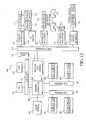
- FIG. 10illustrates a process according to an embodiment of the present invention.
- FIG. 11illustrates an exemplary construction of a resistance variable memory element in accordance with the second embodiment of the invention.
- FIG. 12is a processor based system having one or more memory devices that contains resistance variable memory elements according to the present invention.
- substrateused in the following description may include any supporting structure including, but not limited to, a plastic or a semiconductor substrate that has an exposed substrate surface.
- Semiconductor substratesshould be understood to include silicon, silicon-on-insulator (SOI), silicon-on-sapphire (SOS), doped and undoped semiconductors, epitaxial layers of silicon supported by a base semiconductor foundation, and other semiconductor structures.
- SOIsilicon-on-insulator
- SOSsilicon-on-sapphire
- doped and undoped semiconductorssilicon-on-insulator
- epitaxial layers of silicon supported by a base semiconductor foundationand other semiconductor structures.
- silveris intended to include not only elemental silver, but silver with other trace metals or in various alloyed combinations with other metals as known in the semiconductor industry, as long as such silver alloy is conductive, and as long as the physical and electrical properties of the silver remain unchanged.
- silver-selenideis intended to include various species of silver-selenide, including some species which have a slight excess or deficit of silver, for instance, Ag 2 Se, Ag 2+x Se, and Ag 2 ⁇ x Se.
- semi-volatile memory deviceis intended to include any memory device which is capable of maintaining its memory state after power is removed from the device for a prolonged period of time. Thus, semi-volatile memory devices are capable of retaining stored data after the power source is disconnected or removed.
- semi-volatile memory deviceas used herein includes not only semi-volatile memory devices, but also non-volatile memory devices.
- resistance variable memory elementis intended to include any memory element, including programmable conductor memory elements, semi-volatile memory elements, and non-volatile memory elements which exhibit a resistance change in response to an applied voltage.
- the present inventionrelates to a process for forming a resistance variable memory element.
- the inventionwill now be explained with reference to FIGS. 1 - 10 , which illustrate exemplary embodiments of a resistance variable memory element 100 in accordance with the invention.
- FIG. 10shows an exemplary processing sequence for forming a resistance variable memory element in an exemplary embodiment of the invention.
- a semiconductor substrate 10such as a silicon wafer, is prepared for the processing steps of the present invention.
- a resistance variable memory elementmay be implemented in various different technologies.
- Insulating material 11such as silicon dioxide, is formed over substrate 10 in process segment 108 .
- a first electrode 12is formed over the insulating material 11 .
- the material used to form the electrodecan be selected from a variety of conductive materials, for example, tungsten, nickel, tantalum, titanium, titanium nitride, aluminum, platinum, or silver, among many others.
- an insulating layer 13preferably formed of silicon nitride, is formed over the first electrode 12 .
- This and any other subsequently formed insulating layersmay be formed of a conventional insulating nitride or oxide, among others.
- the present inventionis not limited, however, to the above-listed materials and other insulating and/or dielectric materials known in the industry may be used.
- the insulating layermay be formed by any known deposition methods, for example, by sputtering, chemical vapor deposition (CVD), plasma enhanced CVD (PECVD) or physical vapor deposition (PVD), among others.
- the insulating layer 13is etched to form an opening 22 , which exposes the first electrode 12 . This is done by patterning a masking material 21 and etching to remove unmasked portions of the insulating layer 13 , with the etch stopping once it reaches the first electrode 12 .
- a metal containing layer 31such as silver is formed to substantially fill the opening 22 and contact the first electrode 12 .
- Silver-selenidemay also be used as the metal containing layer 31 .
- the metal containing layer 31is then planarized down to expose the surface of insulating layer 13 , by using an abrasive planarization etching technique, such as chemical mechanical planarization (CMP).
- CMPchemical mechanical planarization
- a partial etchbackpreferably a wet etch, is performed to remove a portion of the metal containing layer from the opening 22 .
- An exemplary wet etchwould incorporate HNO 3 and H 2 O. Regardless of the type of etch used, it is desirable that the metal containing layer 31 is recessed within the opening 22 approximately 50% or less of the depth of opening 22 and preferably is recessed by about 40 to about 50% of the depth, the importance of which will become apparent later in the description of the process.
- Wet etchingis preferred to alleviate the problem of a sidewall forming from etch chemicals. Also, as wet etching is performed down an opening, the isotropic nature of wet etching is not a constraint and the etching is self-aligned to the opening.
- a first resistance variable material 41is formed over the insulating layer 13 and recessed metal containing layer 31 .
- the first resistance variable material 41is deposited in such a manner so as to contact the recessed metal containing layer 31 .
- the first resistance variable material 41is a chalcogenide glass and is preferably a germanium-selenide glass.
- the germanium-selenide glass compositionis preferably one having a Ge x Se 100 ⁇ x stoichiometry of from about Ge 20 Se 80 to about Ge 33 Se 67 , and is more preferably about Ge 25 Se 75 .
- the first resistance variable material 41may be deposited by any known deposition methods, for example, by sputtering, chemical vapor deposition (CVD), plasma enhanced CVD (PECVD) or physical vapor deposition (PVD).
- the substrate 10is either irradiated with light or thermally treated in combination with light irradiation to cause sufficient diffusion of metal ions from recessed metal containing layer 31 into the first resistance variable material 41 .
- the first resistance variable material 41may be irradiated for about 5 to 30 minutes at between about 1 mW/cm 2 to about 10 mW/cm 2 with light at from about 200 nm to about 600 nm wavelength.
- the irradiationmay be used in combination with a thermal process using a temperature of from about 50° C. to about 300° C.
- the irradiation processis sufficient to cause the desired diffusion of metal ions from metal containing layer 31 into layer 41 ; however, the thermal process by itself is not used, but is only used in combination with the irradiation process.
- metal ionsare only incorporated into the resistance variable material within the opening 22 .
- metal ionsare only incorporated into the resistance variable material within the opening 22 .
- a sufficient amount of the metal containing layer 31is available for diffusion of metal ions into the resistance variable material 41 .
- processing the substrate with light irradiationresults in a metal containing resistance variable material 51 being formed in the opening 22 .
- Any residual resistance variable material over layer 13is removed by a dry etch process in processing segment 190 shown in FIG. 10. By removing the residual resistance variable material, further metal doping of the memory element will not occur during subsequent processing and volume expansion stress is reduced.
- the dry etch processis preferably a chemistry containing a gas which is selective between the resistance variable material 41 and the metal containing resistance variable material 51 .
- an exemplary selective dry etch processwould include CF 4 gas and/or SF 6 gas which are selective between Ge 25 Se 75 and Ag x (Ge 25 Se 75 ) 1 ⁇ x , If, by chance, metal is doped into the resistance variable material above or to the side of the opening 22 , the dry etch will not remove it, however, the stress of confining the doped area of the element is relieved through the top of the element resulting in an element that is mushroom shaped at the top of the opening 22 . However, the mushroom shape is not a detriment to electrical performance.
- a second conductive electrode 61is formed over the insulating layer 13 and metal containing resistance variable material 51 to complete the formation of the resistance variable memory element.
- the second electrodeis preferably formed of tungsten, however any suitable conductive materials may be used to form the second electrode 61 .
- the resulting structureforms a resistance variable memory element comprising a metal containing resistance variable material (i.e., such as a silver containing chalcogenide glass layer) and at least two conductive electrodes, namely electrodes 12 and 61 .
- Conventional processing stepscan then be carried out to electrically couple the second electrode 61 to various circuits of memory arrays.
- FIGS. 1 - 8depict a first exemplary embodiment of the invention.
- the structure depicted in FIG. 7can also form the base of a second embodiment of the invention.
- the second embodimentis now described with reference to FIGS. 9 A- 9 C and process segments 300 - 320 of FIG. 10.
- a metal containing layer 71such as silver-selenide, may be deposited over the metal containing resistance variable material 51 .
- Any suitable metal containing layer 71may be used.
- other suitable metal containing layersinclude silver-chalcogenide layers.
- Silver sulfide, silver oxide, and silver tellurideare all suitable silver-chalcogenides that may be used in combination with any suitable metal containing resistance variable material 51 .
- a variety of processescan be used to form the metal containing layer 71 .
- physical vapor deposition techniquessuch as evaporative deposition and sputtering may be used.
- Other processessuch as chemical vapor deposition, co-evaporation or depositing a layer of selenium above a layer of silver to form silver-selenide can also be used.
- a second resistance variable material 81preferably a chalcogenide glass and more preferably a germanium-selenide glass is deposited over the metal containing layer 71 .
- the second germanium-selenide glass compositionis preferably one having a Ge x Se 100 ⁇ x stoichiometry between about Ge 20 Se 80 to about Ge 43 Se 57 and is more preferably about Ge 40 Se 60 .
- the second resistance variable material 41may be deposited by any known deposition methods, for example, by sputtering, chemical vapor deposition (CVD), plasma enhanced CVD (PECVD) or physical vapor deposition (PVD).
- a second conductive electrode 61is formed over the second resistance variable material 81 to complete the formation of a resistance variable memory element in accordance with the second embodiment of the invention.
- the second electrodeis preferably formed of tungsten, however any suitable conductive materials may be used to form the second electrode 61 .
- the resulting structureforms a resistance variable memory element comprising a metal containing resistance variable material 51 (such as a silver-germanium-selenium glass layer), a metal containing layer 71 (such as silver-selenide), a resistance variable material layer 81 (such as a germanium-selenium glass layer), and at least two conductive electrodes, namely electrodes 12 and 61 .
- Conventional processing stepscan then be carried out to electrically couple the first and second electrode 12 , 61 to various circuits of memory arrays.
- Providing a metal containing layer 71 , such as silver-selenide, over the metal containing resistance variable material 51 and then providing a second resistance variable material 81 over the metal containing layer 71allows the metal in the metal containing layer 71 to be more readily available for switching.
- FIG. 11illustrates an exemplary construction of a resistance variable memory element 100 employing the first embodiment of the invention.
- a resistance variable memory element 100 in accordance with the first embodiment of the inventionis generally fabricated over a semiconductor substrate 10 and comprises a first insulating layer 11 formed over a substrate 10 .
- An access transistor 83 for accessing the memory elementis illustrated as having source/drain regions 84 , 85 and a gate stack 86 .
- Access circuitry for operating a resistance variable memory cellmay be fabricated in substrate 10 .
- the insulating layer 11is provided over the circuitry, including transistor 83 and contains a conductive plug 161 .
- a first metal electrode 12is formed within a second insulating layer 8 provided over the insulating layer 11 and plug 161 .
- a third insulating layer 13is formed over the first electrode 12 and second insulating layer 8 .
- an etched openingis provided.
- a metal material and a resistance variable materialare deposited in the opening and processed via light irradiation in accordance with process segments 140 - 190 to form a metal containing resistance variable material 51 in the opening of the third insulating layer 13 .
- the metal containing resistance variable material 51may be a silver-germanium-selenide glass.
- a second metal electrode 54is formed in contact with the silver-germanium-selenide glass 51 .
- the third insulating layer 13may be formed, for example, between the first electrode 12 and the second electrode 54 of any suitable insulator, for example a nitride, an oxide, or other insulator.
- the third insulating layer 13may be formed by any known deposition method, for example, by sputtering, chemical vapor deposition (CVD), plasma enhanced CVD (PECVD) or physical vapor deposition (PVD), among others.
- a preferred insulating materialis silicon nitride, but those skilled in the art will appreciate that there are other numerous suitable insulating materials for this purpose.
- the first electrode 12is electrically connected through conductive plug 161 to a source/drain region 84 of access transistor 83 .
- Source/drain region 85is connected by another conductive plug 87 to other circuitry of a memory array.
- the gate of the transistor 83may be part of a word line which is connected to a plurality of resistance variable memory elements 100 just as a bit line of a memory array may be coupled to a plurality of resistance variable memory elements through plug 87 .
- the resistance variable memory element 100 of the inventionmay be used in a random access memory device.
- FIG. 12illustrates an exemplary processing system 900 which utilizes a resistance variable memory random access device 101 containing an array of resistance variable memory elements 100 constructed as described above with reference to FIGS. 1 - 10 .
- the processing system 900includes one or more processors 901 coupled to a local bus 904 .
- a memory controller 902 and a primary bus bridge 903are also coupled the local bus 904 .
- the processing system 900may include multiple memory controllers 902 and/or multiple primary bus bridges 903 .
- the memory controller 902 and the primary bus bridge 903may be integrated as a single device 906 .
- the memory controller 902is also coupled to one or more memory buses 907 .
- Each memory busaccepts memory components 908 , which include at least one memory device 101 of the invention.
- the memory controller 902may be omitted and the memory components directly coupled to one or more processors 901 .
- the memory components 908may be a memory card or a memory module.
- the memory components 908may include one or more additional devices 909 .
- the additional device 909might be a configuration memory.
- the memory controller 902may also be coupled to a cache memory 905 .
- the cache memory 905may be the only cache memory in the processing system.
- processors 901may also include cache memories, which may form a cache hierarchy with cache memory 905 .
- the processing system 900include peripherals or controllers which are bus masters or which support direct memory access (DMA), the memory controller 902 may implement a cache coherency protocol. If the memory controller 902 is coupled to a plurality of memory buses 907 , each memory bus 907 may be operated in parallel, or different address ranges may be mapped to different memory buses 907 .
- DMAdirect memory access
- the primary bus bridge 903is coupled to at least one peripheral bus 910 .
- Various devicessuch as peripherals or additional bus bridges may be coupled to the peripheral bus 910 . These devices may include a storage controller 911 , an miscellaneous I/O device 914 , a secondary bus bridge 915 , a multimedia processor 918 , and an legacy device interface 920 .
- the primary bus bridge 903may also coupled to one or more special purpose high speed ports 922 . In a personal computer, for example, the special purpose port might be the Accelerated Graphics Port (AGP), used to couple a high performance video card to the processing system 900 .
- AGPAccelerated Graphics Port
- the storage controller 911couples one or more storage devices 913 , via a storage bus 912 , to the peripheral bus 910 .
- the storage controller 911may be a SCSI controller and storage devices 913 may be SCSI discs.
- the I/O device 914may be any sort of peripheral.
- the I/O device 914may be an local area network interface, such as an Ethernet card.
- the secondary bus bridgemay be used to interface additional devices via another bus to the processing system.
- the secondary bus bridgemay be an universal serial port (USB) controller used to couple USB devices 917 via to the processing system 900 .
- USBuniversal serial port
- the multimedia processor 918may be a sound card, a video capture card, or any other type of media interface, which may also be coupled to one additional devices such as speakers 919 .
- the legacy device interface 920is used to couple legacy devices, for example, older styled keyboards and mice, to the processing system 900 .
- FIG. 12illustrates a processing architecture especially suitable for a general purpose computer, such as a personal computer or a workstation, it should be recognized that well known modifications can be made to configure the processing system 900 to become more suitable for use in a variety of applications. For example, many electronic devices which require processing may be implemented using a simpler architecture which relies on a CPU 901 coupled to memory components 908 and/or memory elements 100 .
- These electronic devicesmay include, but are not limited to audio/video processors and recorders, gaming consoles, digital television sets, wired or wireless telephones, navigation devices (including system based on the global positioning system (GPS) and/or inertial navigation), and digital cameras and/or recorders.
- the modificationsmay include, for example, elimination of unnecessary components, addition of specialized devices or circuits, and/or integration of a plurality of devices.
Landscapes
- Engineering & Computer Science (AREA)
- Manufacturing & Machinery (AREA)
- Semiconductor Memories (AREA)
Abstract
Description
- The invention relates to the field of random access memory (RAM) devices formed using a resistance variable material, and in particular to an improved method of manufacturing a resistance variable memory element.[0001]
- A well known semiconductor memory component is a random access memory (RAM). RAM permits repeated read and write operations on memory elements. Typically, RAM devices are volatile, in that stored data is lost once the power source is disconnected or removed. Non-limiting examples of RAM devices include dynamic random access memory (DRAM), synchronized dynamic random access memory (SDRAM) and static random access memory (SRAM). In addition, DRAMS and SDRAMS also typically store data in capacitors which require periodic refreshing to maintain the stored data.[0002]
- Recently resistance variable memory elements, which include programmable conductor memory elements, have been investigated for suitability as semi-volatile and non-volatile random access memory elements. Generally a programmable conductor memory element includes an insulating dielectric material formed of a chalcogenide glass disposed between two electrodes. A conductive material, such as silver, is incorporated into the dielectric material. The resistance of the dielectric material can be changed between high resistance and low resistance states. The programmable conductor memory is normally in a high resistance state when at rest. A write operation to a low resistance state is performed by applying a voltage potential across the two electrodes.[0003]
- When set in a low resistance state, the state of the memory element will remain intact for minutes or longer after the voltage potentials are removed. Such material can be returned to its high resistance state by applying a reverse voltage potential between the electrodes as used to write the element to the low resistance state. Again, the highly resistive state is maintained once the voltage potential is removed. This way, such a device can function, for example, as a resistance variable memory element having two resistance states, which can define two logic states.[0004]
- One preferred resistance variable material comprises a chalcogenide glass, for example, a Ge[0005]xSe100−xglass. One method of forming a resistance variable memory element based on chalcogenide glass includes forming a lower electrode over a substrate, forming an insulating layer over the lower electrode, forming an opening in the insulating layer to expose the lower electrode, forming a metal containing chalcogenide glass in the opening, recessing the metal containing chalcogenide glass, and forming an upper electrode overlying the insulating layer and the recessed metal containing chalcogenide glass. The resistance variable memory element can be recessed using a dry etch or plasma etch. The chemistries used in the dry etch or plasma etch produce inherent sidewalls of chemical compounds on the photo resist or structure used to define the etch which are very difficult to remove.
- A specific example of a metal containing chalcogenide glass is germanium-selenide (Ge[0006]xSe100−x) containing silver (Ag). A method of providing silver to the germanium-selenide composition is to initially form a germanium-selenide glass and then deposit a thin layer of silver upon the glass, for example by sputtering, physical vapor deposition, or other known technique in the art. The layer of silver may be irradiated, preferably with electromagnetic energy at a wavelength less than 600 nanometers, so that the energy passes through the silver and to the silver/glass interface, to break a chalcogenide bond of the chalcogenide material such that the glass is doped with silver. Silver may also be provided to the glass by processing the glass with silver, as in the case of a silver-germanium-selenide glass. Another method for providing metal to the glass is to provide a layer of silver-selenide on a germanium-selenide glass.
- It would be desirable to have an improved method of fabricating a resistance variable memory element, which does not produce undesirable etch chemistry sidewalls.[0007]
- The present invention provides a method of fabricating a resistance variable memory element which inhibits production of undesirable etch chemistry sidewalls. In a first embodiment, the method includes forming an insulating layer over a first electrode; forming an opening in the insulating layer to expose a portion of the first electrode; forming a metal material in the opening; depositing a resistance variable material over the metal material and in the opening; processing the resistance variable material to diffuse metal ions from the metal material into the resistance variable material to form a metal containing resistance variable material in the opening; and forming a second electrode over the insulating layer and over the metal containing resistance variable material.[0008]
- The metal material is preferably silver, the resistance variable material is preferably a germanium-selenium composition, and the resulting metal containing resistance variable material is preferably a silver-germanium-selenium composition.[0009]
- In another embodiment a metal-chalcogenide layer, for example, silver selenide is formed over the metal material and a second resistance variable material, for example a second germanium-selenium composition, is formed over the metal-chalcogenide layer, prior to the formation of the second electrode.[0010]
- These and other features and advantages of the invention will be more apparent from the following detailed description, which is provided in connection with the accompanying drawings and illustrate exemplary embodiments of the invention.[0011]
- FIG. 1 is a cross-sectional view depicting a semiconductor substrate at an initial stage of processing towards a resistance variable memory element.[0012]
- FIG. 2 is a subsequent cross-sectional view taken from FIG. 1 at a stage of processing subsequent to that shown in FIG. 1.[0013]
- FIG. 3 is a subsequent cross-sectional view taken from FIG. 2 at a stage of processing subsequent to that shown in FIG. 2.[0014]
- FIG. 4 is a subsequent cross-sectional view taken from FIG. 3 at a stage of processing subsequent to that shown in FIG. 3.[0015]
- FIG. 5 is a subsequent cross-sectional view taken from FIG. 4 at a stage of processing subsequent to that shown in FIG. 4.[0016]
- FIG. 6 is a subsequent cross-sectional view taken from FIG. 5 at a stage of processing subsequent to that shown in FIG. 5.[0017]
- FIG. 7 is a subsequent cross-sectional view taken from FIG. 6 at a stage of processing subsequent to that shown in FIG. 6.[0018]
- FIG. 8 is a subsequent cross-sectional view taken from FIG. 7 at a stage of processing subsequent to that shown in FIG. 7.[0019]
- FIG. 9A is a subsequent cross-sectional view taken from FIG. 7 at a stage of processing subsequent to that shown in FIG. 7 in accordance with a second embodiment of the invention.[0020]
- FIG. 9B is a subsequent cross-sectional view taken from FIG. 9A at a stage of processing subsequent to that shown in FIG. 9A in accordance with the second embodiment of the invention.[0021]
- FIG. 9C is a subsequent cross-sectional view taken from FIG. 9B at a stage of processing subsequent to that shown in FIG. 9B in accordance with the second embodiment of the invention.[0022]
- FIG. 10 illustrates a process according to an embodiment of the present invention.[0023]
- FIG. 11 illustrates an exemplary construction of a resistance variable memory element in accordance with the second embodiment of the invention.[0024]
- FIG. 12 is a processor based system having one or more memory devices that contains resistance variable memory elements according to the present invention.[0025]
- In the following detailed description, reference is made to various specific structural and process embodiments of the invention. These embodiments are described with sufficient detail to enable those skilled in the art to practice the invention. It is to be understood that other embodiments may be employed, and that various structural, logical and electrical changes may be made without departing from the spirit or scope of the invention.[0026]
- The term “substrate” used in the following description may include any supporting structure including, but not limited to, a plastic or a semiconductor substrate that has an exposed substrate surface. Semiconductor substrates should be understood to include silicon, silicon-on-insulator (SOI), silicon-on-sapphire (SOS), doped and undoped semiconductors, epitaxial layers of silicon supported by a base semiconductor foundation, and other semiconductor structures. When reference is made to a substrate or wafer in the following description, previous process steps may have been utilized to form regions or junctions in or over the base semiconductor or foundation.[0027]
- The term “silver” is intended to include not only elemental silver, but silver with other trace metals or in various alloyed combinations with other metals as known in the semiconductor industry, as long as such silver alloy is conductive, and as long as the physical and electrical properties of the silver remain unchanged.[0028]
- The term “silver-selenide” is intended to include various species of silver-selenide, including some species which have a slight excess or deficit of silver, for instance, Ag[0029]2Se, Ag2+xSe, and Ag2−xSe.
- The term “semi-volatile memory device” is intended to include any memory device which is capable of maintaining its memory state after power is removed from the device for a prolonged period of time. Thus, semi-volatile memory devices are capable of retaining stored data after the power source is disconnected or removed. The term “semi-volatile memory device” as used herein includes not only semi-volatile memory devices, but also non-volatile memory devices.[0030]
- The term “resistance variable memory element” is intended to include any memory element, including programmable conductor memory elements, semi-volatile memory elements, and non-volatile memory elements which exhibit a resistance change in response to an applied voltage.[0031]
- The present invention relates to a process for forming a resistance variable memory element. The invention will now be explained with reference to FIGS.[0032]1-10, which illustrate exemplary embodiments of a resistance
variable memory element 100 in accordance with the invention. FIG. 10 shows an exemplary processing sequence for forming a resistance variable memory element in an exemplary embodiment of the invention. - Referring to FIGS. 1 and 10, a[0033]
semiconductor substrate 10, such as a silicon wafer, is prepared for the processing steps of the present invention. A resistance variable memory element may be implemented in various different technologies. One such application is in memory devices. Insulatingmaterial 11, such as silicon dioxide, is formed oversubstrate 10 inprocess segment 108. Next and as shown atprocess segment 110, afirst electrode 12, is formed over the insulatingmaterial 11. The material used to form the electrode can be selected from a variety of conductive materials, for example, tungsten, nickel, tantalum, titanium, titanium nitride, aluminum, platinum, or silver, among many others. Next and as shown atprocess segment 120, an insulatinglayer 13, preferably formed of silicon nitride, is formed over thefirst electrode 12. This and any other subsequently formed insulating layers may be formed of a conventional insulating nitride or oxide, among others. The present invention is not limited, however, to the above-listed materials and other insulating and/or dielectric materials known in the industry may be used. The insulating layer may be formed by any known deposition methods, for example, by sputtering, chemical vapor deposition (CVD), plasma enhanced CVD (PECVD) or physical vapor deposition (PVD), among others. - Referring now to FIG. 2 and[0034]
processing segment 130 of FIG. 10, the insulatinglayer 13 is etched to form anopening 22, which exposes thefirst electrode 12. This is done by patterning a maskingmaterial 21 and etching to remove unmasked portions of the insulatinglayer 13, with the etch stopping once it reaches thefirst electrode 12. - Referring now to FIG. 3 and[0035]
processing segment 140, the maskingmaterial 21 of FIG. 2 is stripped and ametal containing layer 31, such as silver is formed to substantially fill theopening 22 and contact thefirst electrode 12. Silver-selenide may also be used as themetal containing layer 31. - Referring now to FIG. 4 and[0036]
processing segment 150 of FIG. 10, themetal containing layer 31 is then planarized down to expose the surface of insulatinglayer 13, by using an abrasive planarization etching technique, such as chemical mechanical planarization (CMP). Thus, themetal containing layer 31 is left only in theopening 22. - Referring now to FIG. 5 and[0037]
processing segment 160 of FIG. 10, a partial etchback, preferably a wet etch, is performed to remove a portion of the metal containing layer from theopening 22. An exemplary wet etch would incorporate HNO3and H2O. Regardless of the type of etch used, it is desirable that themetal containing layer 31 is recessed within theopening 22 approximately 50% or less of the depth ofopening 22 and preferably is recessed by about 40 to about 50% of the depth, the importance of which will become apparent later in the description of the process. Wet etching is preferred to alleviate the problem of a sidewall forming from etch chemicals. Also, as wet etching is performed down an opening, the isotropic nature of wet etching is not a constraint and the etching is self-aligned to the opening. - Referring now to FIG. 6 and[0038]
processing segments resistance variable material 41 is formed over the insulatinglayer 13 and recessedmetal containing layer 31. The firstresistance variable material 41 is deposited in such a manner so as to contact the recessedmetal containing layer 31. In an exemplary embodiment, the firstresistance variable material 41 is a chalcogenide glass and is preferably a germanium-selenide glass. The germanium-selenide glass composition is preferably one having a GexSe100−xstoichiometry of from about Ge20Se80to about Ge33Se67, and is more preferably about Ge25Se75. The firstresistance variable material 41 may be deposited by any known deposition methods, for example, by sputtering, chemical vapor deposition (CVD), plasma enhanced CVD (PECVD) or physical vapor deposition (PVD). - In accordance with[0039]
processing segment 180 shown in FIG. 10, and as indicated by arrows in FIG. 6, thesubstrate 10 is either irradiated with light or thermally treated in combination with light irradiation to cause sufficient diffusion of metal ions from recessedmetal containing layer 31 into the firstresistance variable material 41. For example, the firstresistance variable material 41 may be irradiated for about 5 to 30 minutes at between about 1 mW/cm2to about 10 mW/cm2with light at from about 200 nm to about 600 nm wavelength. Additionally, the irradiation may be used in combination with a thermal process using a temperature of from about 50° C. to about 300° C. (depending upon the glass stoichiometry) and preferably about 110° C. for about 5 to about 15 minutes and preferably 10 minutes. The irradiation process is sufficient to cause the desired diffusion of metal ions frommetal containing layer 31 intolayer 41; however, the thermal process by itself is not used, but is only used in combination with the irradiation process. - Because of the confinement of the[0040]
metal containing layer 31, metal ions are only incorporated into the resistance variable material within theopening 22. By recessing themetal containing layer 31 within theopening 22 by about 40% to about 50% inprocessing segment 160, a sufficient amount of themetal containing layer 31 is available for diffusion of metal ions into theresistance variable material 41. - Referring now to FIG. 7, processing the substrate with light irradiation, results in a metal containing resistance[0041]
variable material 51 being formed in theopening 22. Any residual resistance variable material overlayer 13 is removed by a dry etch process inprocessing segment 190 shown in FIG. 10. By removing the residual resistance variable material, further metal doping of the memory element will not occur during subsequent processing and volume expansion stress is reduced. The dry etch process is preferably a chemistry containing a gas which is selective between theresistance variable material 41 and the metal containing resistancevariable material 51. For example, an exemplary selective dry etch process would include CF4gas and/or SF6gas which are selective between Ge25Se75and Agx(Ge25Se75)1−x, If, by chance, metal is doped into the resistance variable material above or to the side of theopening 22, the dry etch will not remove it, however, the stress of confining the doped area of the element is relieved through the top of the element resulting in an element that is mushroom shaped at the top of theopening 22. However, the mushroom shape is not a detriment to electrical performance. - Referring now to FIG. 8 and[0042]
processing segment 200, a secondconductive electrode 61 is formed over the insulatinglayer 13 and metal containing resistancevariable material 51 to complete the formation of the resistance variable memory element. The second electrode is preferably formed of tungsten, however any suitable conductive materials may be used to form thesecond electrode 61. The resulting structure forms a resistance variable memory element comprising a metal containing resistance variable material (i.e., such as a silver containing chalcogenide glass layer) and at least two conductive electrodes, namelyelectrodes second electrode 61 to various circuits of memory arrays. - FIGS.[0043]1-8 depict a first exemplary embodiment of the invention. The structure depicted in FIG. 7 can also form the base of a second embodiment of the invention. The second embodiment is now described with reference to FIGS.9A-9C and process segments300-320 of FIG. 10. As shown in FIG. 9A and
process segment 300 of FIG. 10 ametal containing layer 71, such as silver-selenide, may be deposited over the metal containing resistancevariable material 51. Any suitablemetal containing layer 71 may be used. For instance, other suitable metal containing layers include silver-chalcogenide layers. Silver sulfide, silver oxide, and silver telluride are all suitable silver-chalcogenides that may be used in combination with any suitable metal containing resistancevariable material 51. A variety of processes can be used to form themetal containing layer 71. For instance, physical vapor deposition techniques such as evaporative deposition and sputtering may be used. Other processes such as chemical vapor deposition, co-evaporation or depositing a layer of selenium above a layer of silver to form silver-selenide can also be used. - Referring now to FIG. 9B and[0044]
process segment 310, a secondresistance variable material 81, preferably a chalcogenide glass and more preferably a germanium-selenide glass is deposited over themetal containing layer 71. The second germanium-selenide glass composition is preferably one having a GexSe100−xstoichiometry between about Ge20Se80to about Ge43Se57and is more preferably about Ge40Se60. The secondresistance variable material 41 may be deposited by any known deposition methods, for example, by sputtering, chemical vapor deposition (CVD), plasma enhanced CVD (PECVD) or physical vapor deposition (PVD). - Referring now to FIG. 9C and[0045]
process segment 320 of FIG. 10, a secondconductive electrode 61 is formed over the secondresistance variable material 81 to complete the formation of a resistance variable memory element in accordance with the second embodiment of the invention. The second electrode is preferably formed of tungsten, however any suitable conductive materials may be used to form thesecond electrode 61. - The resulting structure forms a resistance variable memory element comprising a metal containing resistance variable material[0046]51 (such as a silver-germanium-selenium glass layer), a metal containing layer71 (such as silver-selenide), a resistance variable material layer81 (such as a germanium-selenium glass layer), and at least two conductive electrodes, namely
electrodes second electrode metal containing layer 71, such as silver-selenide, over the metal containing resistancevariable material 51 and then providing a secondresistance variable material 81 over themetal containing layer 71 allows the metal in themetal containing layer 71 to be more readily available for switching. - FIG. 11 illustrates an exemplary construction of a resistance[0047]
variable memory element 100 employing the first embodiment of the invention. A resistancevariable memory element 100 in accordance with the first embodiment of the invention is generally fabricated over asemiconductor substrate 10 and comprises a first insulatinglayer 11 formed over asubstrate 10. Anaccess transistor 83 for accessing the memory element is illustrated as having source/drain regions gate stack 86. Access circuitry for operating a resistance variable memory cell may be fabricated insubstrate 10. The insulatinglayer 11 is provided over the circuitry, includingtransistor 83 and contains aconductive plug 161. In accordance withprocess segment 110, afirst metal electrode 12 is formed within a secondinsulating layer 8 provided over the insulatinglayer 11 and plug161. In accordance withprocess segment 120, a third insulatinglayer 13 is formed over thefirst electrode 12 and second insulatinglayer 8. In accordance withprocess segment 130, an etched opening is provided. A metal material and a resistance variable material are deposited in the opening and processed via light irradiation in accordance with process segments140-190 to form a metal containing resistancevariable material 51 in the opening of the third insulatinglayer 13. As described, the metal containing resistancevariable material 51 may be a silver-germanium-selenide glass. - In accordance with process segment[0048]200 a
second metal electrode 54 is formed in contact with the silver-germanium-selenide glass 51. - The third insulating[0049]
layer 13 may be formed, for example, between thefirst electrode 12 and thesecond electrode 54 of any suitable insulator, for example a nitride, an oxide, or other insulator. The third insulatinglayer 13 may be formed by any known deposition method, for example, by sputtering, chemical vapor deposition (CVD), plasma enhanced CVD (PECVD) or physical vapor deposition (PVD), among others. A preferred insulating material is silicon nitride, but those skilled in the art will appreciate that there are other numerous suitable insulating materials for this purpose. - The[0050]
first electrode 12 is electrically connected throughconductive plug 161 to a source/drain region 84 ofaccess transistor 83. Source/drain region 85 is connected by anotherconductive plug 87 to other circuitry of a memory array. The gate of thetransistor 83 may be part of a word line which is connected to a plurality of resistancevariable memory elements 100 just as a bit line of a memory array may be coupled to a plurality of resistance variable memory elements throughplug 87. - The resistance[0051]
variable memory element 100 of the invention may be used in a random access memory device. FIG. 12 illustrates anexemplary processing system 900 which utilizes a resistance variable memoryrandom access device 101 containing an array of resistancevariable memory elements 100 constructed as described above with reference to FIGS.1-10. Theprocessing system 900 includes one ormore processors 901 coupled to alocal bus 904. Amemory controller 902 and aprimary bus bridge 903 are also coupled thelocal bus 904. Theprocessing system 900 may includemultiple memory controllers 902 and/or multiple primary bus bridges903. Thememory controller 902 and theprimary bus bridge 903 may be integrated as asingle device 906. - The[0052]
memory controller 902 is also coupled to one ormore memory buses 907. Each memory bus acceptsmemory components 908, which include at least onememory device 101 of the invention. Alternatively, in a simplified system, thememory controller 902 may be omitted and the memory components directly coupled to one ormore processors 901. Thememory components 908 may be a memory card or a memory module. Thememory components 908 may include one or moreadditional devices 909. For example, theadditional device 909 might be a configuration memory. Thememory controller 902 may also be coupled to acache memory 905. Thecache memory 905 may be the only cache memory in the processing system. Alternatively, other devices, for example,processors 901 may also include cache memories, which may form a cache hierarchy withcache memory 905. If theprocessing system 900 include peripherals or controllers which are bus masters or which support direct memory access (DMA), thememory controller 902 may implement a cache coherency protocol. If thememory controller 902 is coupled to a plurality ofmemory buses 907, eachmemory bus 907 may be operated in parallel, or different address ranges may be mapped todifferent memory buses 907. - The[0053]
primary bus bridge 903 is coupled to at least oneperipheral bus 910. Various devices, such as peripherals or additional bus bridges may be coupled to theperipheral bus 910. These devices may include astorage controller 911, an miscellaneous I/O device 914, asecondary bus bridge 915, amultimedia processor 918, and anlegacy device interface 920. Theprimary bus bridge 903 may also coupled to one or more special purposehigh speed ports 922. In a personal computer, for example, the special purpose port might be the Accelerated Graphics Port (AGP), used to couple a high performance video card to theprocessing system 900. - The[0054]
storage controller 911 couples one ormore storage devices 913, via astorage bus 912, to theperipheral bus 910. For example, thestorage controller 911 may be a SCSI controller andstorage devices 913 may be SCSI discs. The I/O device 914 may be any sort of peripheral. For example, the I/O device 914 may be an local area network interface, such as an Ethernet card. The secondary bus bridge may be used to interface additional devices via another bus to the processing system. For example, the secondary bus bridge may be an universal serial port (USB) controller used to coupleUSB devices 917 via to theprocessing system 900. Themultimedia processor 918 may be a sound card, a video capture card, or any other type of media interface, which may also be coupled to one additional devices such asspeakers 919. Thelegacy device interface 920 is used to couple legacy devices, for example, older styled keyboards and mice, to theprocessing system 900. - The[0055]
processing system 900 illustrated in FIG. 12 is only an exemplary processing system with which the invention may be used. While FIG. 12 illustrates a processing architecture especially suitable for a general purpose computer, such as a personal computer or a workstation, it should be recognized that well known modifications can be made to configure theprocessing system 900 to become more suitable for use in a variety of applications. For example, many electronic devices which require processing may be implemented using a simpler architecture which relies on aCPU 901 coupled tomemory components 908 and/ormemory elements 100. These electronic devices may include, but are not limited to audio/video processors and recorders, gaming consoles, digital television sets, wired or wireless telephones, navigation devices (including system based on the global positioning system (GPS) and/or inertial navigation), and digital cameras and/or recorders. The modifications may include, for example, elimination of unnecessary components, addition of specialized devices or circuits, and/or integration of a plurality of devices. - The above description and drawings are only to be considered illustrative of exemplary embodiments, which achieve the features and advantages of the present invention. Modification and substitutions to specific process conditions and structures can be made without departing from the spirit and scope of the present invention. Accordingly, the invention is not to be considered as being limited by the foregoing description and drawings, but is only limited by the scope of the appended claims.[0056]
Claims (109)
Priority Applications (3)
| Application Number | Priority Date | Filing Date | Title |
|---|---|---|---|
| US10/225,190US7018863B2 (en) | 2002-08-22 | 2002-08-22 | Method of manufacture of a resistance variable memory cell |
| US10/886,676US7459764B2 (en) | 2002-08-22 | 2004-07-09 | Method of manufacture of a PCRAM memory cell |
| US11/430,047US7550818B2 (en) | 2002-08-22 | 2006-05-09 | Method of manufacture of a PCRAM memory cell |
Applications Claiming Priority (1)
| Application Number | Priority Date | Filing Date | Title |
|---|---|---|---|
| US10/225,190US7018863B2 (en) | 2002-08-22 | 2002-08-22 | Method of manufacture of a resistance variable memory cell |
Related Child Applications (1)
| Application Number | Title | Priority Date | Filing Date |
|---|---|---|---|
| US10/886,676DivisionUS7459764B2 (en) | 2002-08-22 | 2004-07-09 | Method of manufacture of a PCRAM memory cell |
Publications (2)
| Publication Number | Publication Date |
|---|---|
| US20040038480A1true US20040038480A1 (en) | 2004-02-26 |
| US7018863B2 US7018863B2 (en) | 2006-03-28 |
Family
ID=31886964
Family Applications (3)
| Application Number | Title | Priority Date | Filing Date |
|---|---|---|---|
| US10/225,190Expired - LifetimeUS7018863B2 (en) | 2002-08-22 | 2002-08-22 | Method of manufacture of a resistance variable memory cell |
| US10/886,676Expired - LifetimeUS7459764B2 (en) | 2002-08-22 | 2004-07-09 | Method of manufacture of a PCRAM memory cell |
| US11/430,047Expired - LifetimeUS7550818B2 (en) | 2002-08-22 | 2006-05-09 | Method of manufacture of a PCRAM memory cell |
Family Applications After (2)
| Application Number | Title | Priority Date | Filing Date |
|---|---|---|---|
| US10/886,676Expired - LifetimeUS7459764B2 (en) | 2002-08-22 | 2004-07-09 | Method of manufacture of a PCRAM memory cell |
| US11/430,047Expired - LifetimeUS7550818B2 (en) | 2002-08-22 | 2006-05-09 | Method of manufacture of a PCRAM memory cell |
Country Status (1)
| Country | Link |
|---|---|
| US (3) | US7018863B2 (en) |
Cited By (8)
| Publication number | Priority date | Publication date | Assignee | Title |
|---|---|---|---|---|
| US20030045054A1 (en)* | 2001-08-29 | 2003-03-06 | Campbell Kristy A. | Method of forming non-volatile resistance variable devices, method of forming a programmable memory cell of memory circuitry, and a non-volatile resistance variable device |
| US20040197976A1 (en)* | 2002-12-30 | 2004-10-07 | Rodgers John C. | Method for manufacturing sidewall contacts for a chalcogenide memory device |
| US20050287698A1 (en)* | 2004-06-28 | 2005-12-29 | Zhiyong Li | Use of chalcogen plasma to form chalcogenide switching materials for nanoscale electronic devices |
| US20070034921A1 (en)* | 2005-08-09 | 2007-02-15 | Micron Technology, Inc. | Access transistor for memory device |
| US20080105861A1 (en)* | 2006-10-03 | 2008-05-08 | Semiconductor Technology Academic Research Center | Multi-value recording phase-change memory device, multi-value recording phase-change channel transistor, and memory cell array |
| US20130234297A1 (en)* | 2012-03-08 | 2013-09-12 | Infineon Technologies Austria Ag | Semiconductor device, wafer assembly and methods of manufacturing wafer assemblies and semiconductor devices |
| US8685783B2 (en) | 2010-10-27 | 2014-04-01 | Taiwan Semiconductor Manufacturing Company, Ltd. | Phase change memory cell |
| US20170162783A1 (en)* | 2015-12-08 | 2017-06-08 | Crossbar, Inc. | Regulating interface layer formation for two-terminal memory |
Families Citing this family (18)
| Publication number | Priority date | Publication date | Assignee | Title |
|---|---|---|---|---|
| US20060045974A1 (en)* | 2004-08-25 | 2006-03-02 | Campbell Kristy A | Wet chemical method to form silver-rich silver-selenide |
| DE102004041626B4 (en)* | 2004-08-27 | 2008-06-05 | Qimonda Ag | Chip card, and chip card security device |
| JP2006165553A (en)* | 2004-12-02 | 2006-06-22 | Samsung Electronics Co Ltd | Phase change memory device including phase change material layer including phase change nanoparticles and method of manufacturing the same |
| US8049202B2 (en) | 2004-12-02 | 2011-11-01 | Samsung Electronics Co., Ltd. | Phase change memory device having phase change material layer containing phase change nano particles |
| WO2006069082A2 (en)* | 2004-12-20 | 2006-06-29 | Bionopoly Llc | Access keys |
| DE102005012047A1 (en)* | 2005-03-16 | 2006-09-28 | Infineon Technologies Ag | Solid-state electrolyte memory manufacture involves coating first electrode with solid-state electrolyte layer, and then forming second electrode on solid-state electrolyte layer |
| US7638357B2 (en)* | 2006-08-25 | 2009-12-29 | Micron Technology, Inc. | Programmable resistance memory devices and systems using the same and methods of forming the same |
| WO2008088599A2 (en) | 2006-10-19 | 2008-07-24 | Boise State University | Forced ion migration for chalcogenide phase change memory device |
| KR100785032B1 (en) | 2006-11-29 | 2007-12-12 | 삼성전자주식회사 | Resistive memory device and manufacturing method thereof |
| US7718533B2 (en)* | 2007-05-08 | 2010-05-18 | Micron Technology, Inc. | Inverted variable resistance memory cell and method of making the same |
| KR20090090563A (en)* | 2008-02-21 | 2009-08-26 | 삼성전자주식회사 | Semiconductor Devices Including Resistive Memory Elements |
| US8238146B2 (en)* | 2008-08-01 | 2012-08-07 | Boise State University | Variable integrated analog resistor |
| US8467236B2 (en) | 2008-08-01 | 2013-06-18 | Boise State University | Continuously variable resistor |
| US20100090749A1 (en)* | 2008-10-09 | 2010-04-15 | United Microelectronics Corp. | Multi-function chip |
| US8064247B2 (en)* | 2009-01-14 | 2011-11-22 | Macronix International Co., Ltd. | Rewritable memory device based on segregation/re-absorption |
| US20110079709A1 (en)* | 2009-10-07 | 2011-04-07 | Campbell Kristy A | Wide band sensor |
| US8284590B2 (en) | 2010-05-06 | 2012-10-09 | Boise State University | Integratable programmable capacitive device |
| US10319908B2 (en)* | 2014-05-01 | 2019-06-11 | Crossbar, Inc. | Integrative resistive memory in backend metal layers |
Citations (93)
| Publication number | Priority date | Publication date | Assignee | Title |
|---|---|---|---|---|
| US449557A (en)* | 1891-03-31 | Plumb-level | ||
| US3961314A (en)* | 1974-03-05 | 1976-06-01 | Energy Conversion Devices, Inc. | Structure and method for producing an image |
| US3966317A (en)* | 1974-04-08 | 1976-06-29 | Energy Conversion Devices, Inc. | Dry process production of archival microform records from hard copy |
| US4267261A (en)* | 1971-07-15 | 1981-05-12 | Energy Conversion Devices, Inc. | Method for full format imaging |
| US4269935A (en)* | 1979-07-13 | 1981-05-26 | Ionomet Company, Inc. | Process of doping silver image in chalcogenide layer |
| US4312938A (en)* | 1979-07-06 | 1982-01-26 | Drexler Technology Corporation | Method for making a broadband reflective laser recording and data storage medium with absorptive underlayer |
| US4316946A (en)* | 1979-12-03 | 1982-02-23 | Ionomet Company, Inc. | Surface sensitized chalcogenide product and process for making and using the same |
| US4320191A (en)* | 1978-11-07 | 1982-03-16 | Nippon Telegraph & Telephone Public Corporation | Pattern-forming process |
| US4499557A (en)* | 1980-10-28 | 1985-02-12 | Energy Conversion Devices, Inc. | Programmable cell for use in programmable electronic arrays |
| US4637895A (en)* | 1985-04-01 | 1987-01-20 | Energy Conversion Devices, Inc. | Gas mixtures for the vapor deposition of semiconductor material |
| US4646266A (en)* | 1984-09-28 | 1987-02-24 | Energy Conversion Devices, Inc. | Programmable semiconductor structures and methods for using the same |
| US4664939A (en)* | 1985-04-01 | 1987-05-12 | Energy Conversion Devices, Inc. | Vertical semiconductor processor |
| US4668968A (en)* | 1984-05-14 | 1987-05-26 | Energy Conversion Devices, Inc. | Integrated circuit compatible thin film field effect transistor and method of making same |
| US4670763A (en)* | 1984-05-14 | 1987-06-02 | Energy Conversion Devices, Inc. | Thin film field effect transistor |
| US4671618A (en)* | 1986-05-22 | 1987-06-09 | Wu Bao Gang | Liquid crystalline-plastic material having submillisecond switch times and extended memory |
| US4673957A (en)* | 1984-05-14 | 1987-06-16 | Energy Conversion Devices, Inc. | Integrated circuit compatible thin film field effect transistor and method of making same |
| US4728406A (en)* | 1986-08-18 | 1988-03-01 | Energy Conversion Devices, Inc. | Method for plasma - coating a semiconductor body |
| US4737379A (en)* | 1982-09-24 | 1988-04-12 | Energy Conversion Devices, Inc. | Plasma deposited coatings, and low temperature plasma method of making same |
| US4795657A (en)* | 1984-04-13 | 1989-01-03 | Energy Conversion Devices, Inc. | Method of fabricating a programmable array |
| US4800526A (en)* | 1987-05-08 | 1989-01-24 | Gaf Corporation | Memory element for information storage and retrieval system and associated process |
| US4804490A (en)* | 1987-10-13 | 1989-02-14 | Energy Conversion Devices, Inc. | Method of fabricating stabilized threshold switching material |
| US4809044A (en)* | 1986-08-22 | 1989-02-28 | Energy Conversion Devices, Inc. | Thin film overvoltage protection devices |
| US4818717A (en)* | 1986-06-27 | 1989-04-04 | Energy Conversion Devices, Inc. | Method for making electronic matrix arrays |
| US4843443A (en)* | 1984-05-14 | 1989-06-27 | Energy Conversion Devices, Inc. | Thin film field effect transistor and method of making same |
| US4891330A (en)* | 1987-07-27 | 1990-01-02 | Energy Conversion Devices, Inc. | Method of fabricating n-type and p-type microcrystalline semiconductor alloy material including band gap widening elements |
| US4920078A (en)* | 1989-06-02 | 1990-04-24 | Bell Communications Research, Inc. | Arsenic sulfide surface passivation of III-V semiconductors |
| US5177567A (en)* | 1991-07-19 | 1993-01-05 | Energy Conversion Devices, Inc. | Thin-film structure for chalcogenide electrical switching devices and process therefor |
| US5219788A (en)* | 1991-02-25 | 1993-06-15 | Ibm Corporation | Bilayer metallization cap for photolithography |
| US5296716A (en)* | 1991-01-18 | 1994-03-22 | Energy Conversion Devices, Inc. | Electrically erasable, directly overwritable, multibit single cell memory elements and arrays fabricated therefrom |
| US5315131A (en)* | 1990-11-22 | 1994-05-24 | Matsushita Electric Industrial Co., Ltd. | Electrically reprogrammable nonvolatile memory device |
| US5314772A (en)* | 1990-10-09 | 1994-05-24 | Arizona Board Of Regents | High resolution, multi-layer resist for microlithography and method therefor |
| US5406509A (en)* | 1991-01-18 | 1995-04-11 | Energy Conversion Devices, Inc. | Electrically erasable, directly overwritable, multibit single cell memory elements and arrays fabricated therefrom |
| US5414271A (en)* | 1991-01-18 | 1995-05-09 | Energy Conversion Devices, Inc. | Electrically erasable memory elements having improved set resistance stability |
| US5500532A (en)* | 1994-08-18 | 1996-03-19 | Arizona Board Of Regents | Personal electronic dosimeter |
| US5512328A (en)* | 1992-08-07 | 1996-04-30 | Hitachi, Ltd. | Method for forming a pattern and forming a thin film used in pattern formation |
| US5512773A (en)* | 1993-12-23 | 1996-04-30 | U.S. Philips Corporation | Switching element with memory provided with Schottky tunnelling barrier |
| US5591501A (en)* | 1995-12-20 | 1997-01-07 | Energy Conversion Devices, Inc. | Optical recording medium having a plurality of discrete phase change data recording points |
| US5596522A (en)* | 1991-01-18 | 1997-01-21 | Energy Conversion Devices, Inc. | Homogeneous compositions of microcrystalline semiconductor material, semiconductor devices and directly overwritable memory elements fabricated therefrom, and arrays fabricated from the memory elements |
| US5714768A (en)* | 1995-10-24 | 1998-02-03 | Energy Conversion Devices, Inc. | Second-layer phase change memory array on top of a logic device |
| US5726083A (en)* | 1994-11-29 | 1998-03-10 | Nec Corporation | Process of fabricating dynamic random access memory device having storage capacitor low in contact resistance and small in leakage current through tantalum oxide film |
| US5751012A (en)* | 1995-06-07 | 1998-05-12 | Micron Technology, Inc. | Polysilicon pillar diode for use in a non-volatile memory cell |
| US5761115A (en)* | 1996-05-30 | 1998-06-02 | Axon Technologies Corporation | Programmable metallization cell structure and method of making same |
| US5869843A (en)* | 1995-06-07 | 1999-02-09 | Micron Technology, Inc. | Memory array having a multi-state element and method for forming such array or cells thereof |
| US6011757A (en)* | 1998-01-27 | 2000-01-04 | Ovshinsky; Stanford R. | Optical recording media having increased erasability |
| US6031287A (en)* | 1997-06-18 | 2000-02-29 | Micron Technology, Inc. | Contact structure and memory element incorporating the same |
| US6177338B1 (en)* | 1999-02-08 | 2001-01-23 | Taiwan Semiconductor Manufacturing Company | Two step barrier process |
| US6236059B1 (en)* | 1996-08-22 | 2001-05-22 | Micron Technology, Inc. | Memory cell incorporating a chalcogenide element and method of making same |
| US20020000666A1 (en)* | 1998-08-31 | 2002-01-03 | Michael N. Kozicki | Self-repairing interconnections for electrical circuits |
| US6339544B1 (en)* | 2000-09-29 | 2002-01-15 | Intel Corporation | Method to enhance performance of thermal resistor device |
| US6348365B1 (en)* | 2001-03-02 | 2002-02-19 | Micron Technology, Inc. | PCRAM cell manufacturing |
| US6350679B1 (en)* | 1999-08-03 | 2002-02-26 | Micron Technology, Inc. | Methods of providing an interlevel dielectric layer intermediate different elevation conductive metal layers in the fabrication of integrated circuitry |
| US6376284B1 (en)* | 1996-02-23 | 2002-04-23 | Micron Technology, Inc. | Method of fabricating a memory device |
| US6391688B1 (en)* | 1995-06-07 | 2002-05-21 | Micron Technology, Inc. | Method for fabricating an array of ultra-small pores for chalcogenide memory cells |
| US20030001229A1 (en)* | 2001-03-01 | 2003-01-02 | Moore John T. | Chalcogenide comprising device |
| US6507061B1 (en)* | 2001-08-31 | 2003-01-14 | Intel Corporation | Multiple layer phase-change memory |
| US6511862B2 (en)* | 2001-06-30 | 2003-01-28 | Ovonyx, Inc. | Modified contact for programmable devices |
| US6512241B1 (en)* | 2001-12-31 | 2003-01-28 | Intel Corporation | Phase change material memory device |
| US6511867B2 (en)* | 2001-06-30 | 2003-01-28 | Ovonyx, Inc. | Utilizing atomic layer deposition for programmable device |
| US6514805B2 (en)* | 2001-06-30 | 2003-02-04 | Intel Corporation | Trench sidewall profile for device isolation |
| US20030027416A1 (en)* | 2001-08-01 | 2003-02-06 | Moore John T. | Method of forming integrated circuitry, method of forming memory circuitry, and method of forming random access memory circuitry |
| US20030032254A1 (en)* | 2000-12-08 | 2003-02-13 | Gilton Terry L. | Resistance variable device, analog memory device, and programmable memory cell |
| US20030035315A1 (en)* | 2001-04-06 | 2003-02-20 | Kozicki Michael N. | Microelectronic device, structure, and system, including a memory structure having a variable programmable property and method of forming the same |
| US20030035314A1 (en)* | 1998-12-04 | 2003-02-20 | Kozicki Michael N. | Programmable microelectronic devices and methods of forming and programming same |
| US20030038301A1 (en)* | 2001-08-27 | 2003-02-27 | John Moore | Apparatus and method for dual cell common electrode PCRAM memory device |
| US20030043631A1 (en)* | 2001-08-30 | 2003-03-06 | Gilton Terry L. | Method of retaining memory state in a programmable conductor RAM |
| US20030045049A1 (en)* | 2001-08-29 | 2003-03-06 | Campbell Kristy A. | Method of forming chalcogenide comprising devices |
| US20030045054A1 (en)* | 2001-08-29 | 2003-03-06 | Campbell Kristy A. | Method of forming non-volatile resistance variable devices, method of forming a programmable memory cell of memory circuitry, and a non-volatile resistance variable device |
| US6531373B2 (en)* | 2000-12-27 | 2003-03-11 | Ovonyx, Inc. | Method of forming a phase-change memory cell using silicon on insulator low electrode in charcogenide elements |
| US20030047765A1 (en)* | 2001-08-30 | 2003-03-13 | Campbell Kristy A. | Stoichiometry for chalcogenide glasses useful for memory devices and method of formation |
| US20030048744A1 (en)* | 2001-09-01 | 2003-03-13 | Ovshinsky Stanford R. | Increased data storage in optical data storage and retrieval systems using blue lasers and/or plasmon lenses |
| US20030048519A1 (en)* | 2000-02-11 | 2003-03-13 | Kozicki Michael N. | Microelectronic photonic structure and device and method of forming the same |
| US20030049912A1 (en)* | 2001-08-29 | 2003-03-13 | Campbell Kristy A. | Method of forming chalcogenide comprsing devices and method of forming a programmable memory cell of memory circuitry |
| US20030047773A1 (en)* | 2001-03-15 | 2003-03-13 | Jiutao Li | Agglomeration elimination for metal sputter deposition of chalcogenides |
| US6534781B2 (en)* | 2000-12-26 | 2003-03-18 | Ovonyx, Inc. | Phase-change memory bipolar array utilizing a single shallow trench isolation for creating an individual active area region for two memory array elements and one bipolar base contact |
| US6545907B1 (en)* | 2001-10-30 | 2003-04-08 | Ovonyx, Inc. | Technique and apparatus for performing write operations to a phase change material memory device |
| US6545287B2 (en)* | 2001-09-07 | 2003-04-08 | Intel Corporation | Using selective deposition to form phase-change memory cells |
| US20030068861A1 (en)* | 2001-08-30 | 2003-04-10 | Jiutao Li | Integrated circuit device and fabrication using metal-doped chalcogenide materials |
| US6555860B2 (en)* | 2000-09-29 | 2003-04-29 | Intel Corporation | Compositionally modified resistive electrode |
| US6563164B2 (en)* | 2000-09-29 | 2003-05-13 | Ovonyx, Inc. | Compositionally modified resistive electrode |
| US6567293B1 (en)* | 2000-09-29 | 2003-05-20 | Ovonyx, Inc. | Single level metal memory cell using chalcogenide cladding |
| US6566700B2 (en)* | 2001-10-11 | 2003-05-20 | Ovonyx, Inc. | Carbon-containing interfacial layer for phase-change memory |
| US20030095426A1 (en)* | 2001-11-20 | 2003-05-22 | Glen Hush | Complementary bit PCRAM sense amplifier and method of operation |
| US20030096497A1 (en)* | 2001-11-19 | 2003-05-22 | Micron Technology, Inc. | Electrode structure for use in an integrated circuit |
| US6570784B2 (en)* | 2001-06-29 | 2003-05-27 | Ovonyx, Inc. | Programming a phase-change material memory |
| US6569705B2 (en)* | 2000-12-21 | 2003-05-27 | Intel Corporation | Metal structure for a phase-change memory device |
| US6673648B2 (en)* | 2001-11-08 | 2004-01-06 | Intel Corporation | Isolating phase change material memory cells |
| US6673700B2 (en)* | 2001-06-30 | 2004-01-06 | Ovonyx, Inc. | Reduced area intersection between electrode and programming element |
| US6687427B2 (en)* | 2000-12-29 | 2004-02-03 | Intel Corporation | Optic switch |
| US6690026B2 (en)* | 2001-09-28 | 2004-02-10 | Intel Corporation | Method of fabricating a three-dimensional array of active media |
| US6696355B2 (en)* | 2000-12-14 | 2004-02-24 | Ovonyx, Inc. | Method to selectively increase the top resistance of the lower programming electrode in a phase-change memory |
| US20040035401A1 (en)* | 2002-08-26 | 2004-02-26 | Subramanian Ramachandran | Hydrogen powered scooter |
| US6707712B2 (en)* | 2001-08-02 | 2004-03-16 | Intel Corporation | Method for reading a structural phase-change memory |
| US6714954B2 (en)* | 2002-05-10 | 2004-03-30 | Energy Conversion Devices, Inc. | Methods of factoring and modular arithmetic |
Family Cites Families (98)
| Publication number | Priority date | Publication date | Assignee | Title |
|---|---|---|---|---|
| US650111A (en)* | 1899-08-31 | 1900-05-22 | Eclipse Automobile Company | Steam-reheater. |
| US3271591A (en) | 1963-09-20 | 1966-09-06 | Energy Conversion Devices Inc | Symmetrical current controlling device |
| US3622319A (en) | 1966-10-20 | 1971-11-23 | Western Electric Co | Nonreflecting photomasks and methods of making same |
| US3868651A (en) | 1970-08-13 | 1975-02-25 | Energy Conversion Devices Inc | Method and apparatus for storing and reading data in a memory having catalytic material to initiate amorphous to crystalline change in memory structure |
| US3743847A (en) | 1971-06-01 | 1973-07-03 | Motorola Inc | Amorphous silicon film as a uv filter |
| US4177474A (en) | 1977-05-18 | 1979-12-04 | Energy Conversion Devices, Inc. | High temperature amorphous semiconductor member and method of making the same |
| DE2901303C2 (en) | 1979-01-15 | 1984-04-19 | Max Planck Gesellschaft Zur Foerderung Der Wissenschaften E.V., 3400 Goettingen | Solid ionic conductor material, its use and process for its manufacture |
| JPS6024580B2 (en) | 1980-03-10 | 1985-06-13 | 日本電信電話株式会社 | Manufacturing method for semiconductor devices |
| US4405710A (en) | 1981-06-22 | 1983-09-20 | Cornell Research Foundation, Inc. | Ion beam exposure of (g-Gex -Se1-x) inorganic resists |
| US4545111A (en) | 1983-01-18 | 1985-10-08 | Energy Conversion Devices, Inc. | Method for making, parallel preprogramming or field programming of electronic matrix arrays |
| US4608296A (en) | 1983-12-06 | 1986-08-26 | Energy Conversion Devices, Inc. | Superconducting films and devices exhibiting AC to DC conversion |
| US4769338A (en) | 1984-05-14 | 1988-09-06 | Energy Conversion Devices, Inc. | Thin film field effect transistor and method of making same |
| US4678679A (en) | 1984-06-25 | 1987-07-07 | Energy Conversion Devices, Inc. | Continuous deposition of activated process gases |
| US4710899A (en) | 1985-06-10 | 1987-12-01 | Energy Conversion Devices, Inc. | Data storage medium incorporating a transition metal for increased switching speed |
| US4766471A (en) | 1986-01-23 | 1988-08-23 | Energy Conversion Devices, Inc. | Thin film electro-optical devices |
| US4845533A (en) | 1986-08-22 | 1989-07-04 | Energy Conversion Devices, Inc. | Thin film electrical devices with amorphous carbon electrodes and method of making same |
| US4853785A (en) | 1986-10-15 | 1989-08-01 | Energy Conversion Devices, Inc. | Electronic camera including electronic signal storage cartridge |
| US4788594A (en) | 1986-10-15 | 1988-11-29 | Energy Conversion Devices, Inc. | Solid state electronic camera including thin film matrix of photosensors |
| US4847674A (en) | 1987-03-10 | 1989-07-11 | Advanced Micro Devices, Inc. | High speed interconnect system with refractory non-dogbone contacts and an active electromigration suppression mechanism |
| US4775425A (en) | 1987-07-27 | 1988-10-04 | Energy Conversion Devices, Inc. | P and n-type microcrystalline semiconductor alloy material including band gap widening elements, devices utilizing same |
| US5272359A (en) | 1988-04-07 | 1993-12-21 | California Institute Of Technology | Reversible non-volatile switch based on a TCNQ charge transfer complex |
| GB8910854D0 (en) | 1989-05-11 | 1989-06-28 | British Petroleum Co Plc | Semiconductor device |
| US5159661A (en) | 1990-10-05 | 1992-10-27 | Energy Conversion Devices, Inc. | Vertically interconnected parallel distributed processor |
| US5330630A (en) | 1991-01-02 | 1994-07-19 | Energy Conversion Devices, Inc. | Switch with improved threshold voltage |
| US5341328A (en) | 1991-01-18 | 1994-08-23 | Energy Conversion Devices, Inc. | Electrically erasable memory elements having reduced switching current requirements and increased write/erase cycle life |
| US5536947A (en) | 1991-01-18 | 1996-07-16 | Energy Conversion Devices, Inc. | Electrically erasable, directly overwritable, multibit single cell memory element and arrays fabricated therefrom |
| US5534712A (en) | 1991-01-18 | 1996-07-09 | Energy Conversion Devices, Inc. | Electrically erasable memory elements characterized by reduced current and improved thermal stability |
| US5534711A (en) | 1991-01-18 | 1996-07-09 | Energy Conversion Devices, Inc. | Electrically erasable, directly overwritable, multibit single cell memory elements and arrays fabricated therefrom |
| US5335219A (en) | 1991-01-18 | 1994-08-02 | Ovshinsky Stanford R | Homogeneous composition of microcrystalline semiconductor material, semiconductor devices and directly overwritable memory elements fabricated therefrom, and arrays fabricated from the memory elements |
| US5166758A (en) | 1991-01-18 | 1992-11-24 | Energy Conversion Devices, Inc. | Electrically erasable phase change memory |
| US5128099A (en) | 1991-02-15 | 1992-07-07 | Energy Conversion Devices, Inc. | Congruent state changeable optical memory material and device |
| US5359205A (en) | 1991-11-07 | 1994-10-25 | Energy Conversion Devices, Inc. | Electrically erasable memory elements characterized by reduced current and improved thermal stability |
| US5238862A (en) | 1992-03-18 | 1993-08-24 | Micron Technology, Inc. | Method of forming a stacked capacitor with striated electrode |
| US5350484A (en) | 1992-09-08 | 1994-09-27 | Intel Corporation | Method for the anisotropic etching of metal films in the fabrication of interconnects |
| US5479319A (en)* | 1992-12-30 | 1995-12-26 | Interconnect Systems, Inc. | Multi-level assemblies for interconnecting integrated circuits |
| US5818749A (en) | 1993-08-20 | 1998-10-06 | Micron Technology, Inc. | Integrated circuit memory device |
| US5543737A (en) | 1995-02-10 | 1996-08-06 | Energy Conversion Devices, Inc. | Logical operation circuit employing two-terminal chalcogenide switches |
| US5789758A (en) | 1995-06-07 | 1998-08-04 | Micron Technology, Inc. | Chalcogenide memory cell with a plurality of chalcogenide electrodes |
| AU6048896A (en) | 1995-06-07 | 1996-12-30 | Micron Technology, Inc. | A stack/trench diode for use with a multi-state material in a non-volatile memory cell |
| US6420725B1 (en) | 1995-06-07 | 2002-07-16 | Micron Technology, Inc. | Method and apparatus for forming an integrated circuit electrode having a reduced contact area |
| US5837564A (en) | 1995-11-01 | 1998-11-17 | Micron Technology, Inc. | Method for optimal crystallization to obtain high electrical performance from chalcogenides |
| US5694054A (en) | 1995-11-28 | 1997-12-02 | Energy Conversion Devices, Inc. | Integrated drivers for flat panel displays employing chalcogenide logic elements |
| US5687112A (en) | 1996-04-19 | 1997-11-11 | Energy Conversion Devices, Inc. | Multibit single cell memory element having tapered contact |
| US5852870A (en) | 1996-04-24 | 1998-12-29 | Amkor Technology, Inc. | Method of making grid array assembly |
| US5851882A (en) | 1996-05-06 | 1998-12-22 | Micron Technology, Inc. | ZPROM manufacture and design and methods for forming thin structures using spacers as an etching mask |
| US5789277A (en) | 1996-07-22 | 1998-08-04 | Micron Technology, Inc. | Method of making chalogenide memory device |
| US5814527A (en) | 1996-07-22 | 1998-09-29 | Micron Technology, Inc. | Method of making small pores defined by a disposable internal spacer for use in chalcogenide memories |
| US5825046A (en) | 1996-10-28 | 1998-10-20 | Energy Conversion Devices, Inc. | Composite memory material comprising a mixture of phase-change memory material and dielectric material |
| US6087674A (en) | 1996-10-28 | 2000-07-11 | Energy Conversion Devices, Inc. | Memory element with memory material comprising phase-change material and dielectric material |
| US5846889A (en) | 1997-03-14 | 1998-12-08 | The United States Of America As Represented By The Secretary Of The Navy | Infrared transparent selenide glasses |
| US5998066A (en) | 1997-05-16 | 1999-12-07 | Aerial Imaging Corporation | Gray scale mask and depth pattern transfer technique using inorganic chalcogenide glass |
| US5933365A (en) | 1997-06-19 | 1999-08-03 | Energy Conversion Devices, Inc. | Memory element with energy control mechanism |
| US6051511A (en) | 1997-07-31 | 2000-04-18 | Micron Technology, Inc. | Method and apparatus for reducing isolation stress in integrated circuits |
| WO1999028914A2 (en)* | 1997-12-04 | 1999-06-10 | Axon Technologies Corporation | Programmable sub-surface aggregating metallization structure and method of making same |
| US6297170B1 (en) | 1998-06-23 | 2001-10-02 | Vlsi Technology, Inc. | Sacrificial multilayer anti-reflective coating for mos gate formation |
| US6141241A (en) | 1998-06-23 | 2000-10-31 | Energy Conversion Devices, Inc. | Universal memory element with systems employing same and apparatus and method for reading, writing and programming same |
| US5912839A (en) | 1998-06-23 | 1999-06-15 | Energy Conversion Devices, Inc. | Universal memory element and method of programming same |
| US6469364B1 (en) | 1998-08-31 | 2002-10-22 | Arizona Board Of Regents | Programmable interconnection system for electrical circuits |
| US6635914B2 (en) | 2000-09-08 | 2003-10-21 | Axon Technologies Corp. | Microelectronic programmable device and methods of forming and programming the same |
| CA2362283A1 (en) | 1999-02-11 | 2000-08-17 | Arizona Board Of Regents | Programmable microelectronic devices and methods of forming and programming same |
| US6072716A (en) | 1999-04-14 | 2000-06-06 | Massachusetts Institute Of Technology | Memory structures and methods of making same |
| US6143604A (en) | 1999-06-04 | 2000-11-07 | Taiwan Semiconductor Manufacturing Company | Method for fabricating small-size two-step contacts for word-line strapping on dynamic random access memory (DRAM) |
| US6423628B1 (en) | 1999-10-22 | 2002-07-23 | Lsi Logic Corporation | Method of forming integrated circuit structure having low dielectric constant material and having silicon oxynitride caps over closely spaced apart metal lines |
| US6865117B2 (en) | 2000-02-11 | 2005-03-08 | Axon Technologies Corporation | Programming circuit for a programmable microelectronic device, system including the circuit, and method of forming the same |
| US6501111B1 (en) | 2000-06-30 | 2002-12-31 | Intel Corporation | Three-dimensional (3D) programmable device |
| US6563156B2 (en) | 2001-03-15 | 2003-05-13 | Micron Technology, Inc. | Memory elements and methods for making same |
| US6440837B1 (en) | 2000-07-14 | 2002-08-27 | Micron Technology, Inc. | Method of forming a contact structure in a semiconductor device |
| WO2002021542A1 (en) | 2000-09-08 | 2002-03-14 | Axon Technologies Corporation | Microelectronic programmable device and methods of forming and programming the same |
| US6404665B1 (en) | 2000-09-29 | 2002-06-11 | Intel Corporation | Compositionally modified resistive electrode |
| US6429064B1 (en) | 2000-09-29 | 2002-08-06 | Intel Corporation | Reduced contact area of sidewall conductor |
| US6649928B2 (en) | 2000-12-13 | 2003-11-18 | Intel Corporation | Method to selectively remove one side of a conductive bottom electrode of a phase-change memory cell and structure obtained thereby |
| US6437383B1 (en) | 2000-12-21 | 2002-08-20 | Intel Corporation | Dual trench isolation for a phase-change memory cell and method of making same |
| US6646297B2 (en) | 2000-12-26 | 2003-11-11 | Ovonyx, Inc. | Lower electrode isolation in a double-wide trench |
| US6638820B2 (en) | 2001-02-08 | 2003-10-28 | Micron Technology, Inc. | Method of forming chalcogenide comprising devices, method of precluding diffusion of a metal into adjacent chalcogenide material, and chalcogenide comprising devices |
| US6818481B2 (en) | 2001-03-07 | 2004-11-16 | Micron Technology, Inc. | Method to manufacture a buried electrode PCRAM cell |
| US6473332B1 (en) | 2001-04-04 | 2002-10-29 | The University Of Houston System | Electrically variable multi-state resistance computing |
| KR100900080B1 (en) | 2001-05-07 | 2009-06-01 | 어드밴스드 마이크로 디바이시즈, 인코포레이티드 | Memory device having self-assembled polymer film and manufacturing method thereof |
| US7102150B2 (en) | 2001-05-11 | 2006-09-05 | Harshfield Steven T | PCRAM memory cell and method of making same |
| US6480438B1 (en) | 2001-06-12 | 2002-11-12 | Ovonyx, Inc. | Providing equal cell programming conditions across a large and high density array of phase-change memory cells |
| US6589714B2 (en) | 2001-06-26 | 2003-07-08 | Ovonyx, Inc. | Method for making programmable resistance memory element using silylated photoresist |
| US6613604B2 (en) | 2001-08-02 | 2003-09-02 | Ovonyx, Inc. | Method for making small pore for use in programmable resistance memory element |
| US6487113B1 (en) | 2001-06-29 | 2002-11-26 | Ovonyx, Inc. | Programming a phase-change memory with slow quench time |
| US6462984B1 (en) | 2001-06-29 | 2002-10-08 | Intel Corporation | Biasing scheme of floating unselected wordlines and bitlines of a diode-based memory array |
| US6605527B2 (en) | 2001-06-30 | 2003-08-12 | Intel Corporation | Reduced area intersection between electrode and programming element |
| US6642102B2 (en) | 2001-06-30 | 2003-11-04 | Intel Corporation | Barrier material encapsulation of programmable material |
| US6586761B2 (en) | 2001-09-07 | 2003-07-01 | Intel Corporation | Phase change material memory device |
| WO2003028098A2 (en) | 2001-09-26 | 2003-04-03 | Axon Technologies Corporation | Programmable chip-to-substrate interconnect structure and device and method of forming same |
| WO2003032392A2 (en) | 2001-10-09 | 2003-04-17 | Axon Technologies Corporation | Programmable microelectronic device, structure, and system, and method of forming the same |
| EP1440485B1 (en) | 2001-10-26 | 2006-06-21 | Arizona Board of Regents | Programmable surface control devices and method of using same |
| US6873538B2 (en) | 2001-12-20 | 2005-03-29 | Micron Technology, Inc. | Programmable conductor random access memory and a method for writing thereto |
| US6625054B2 (en) | 2001-12-28 | 2003-09-23 | Intel Corporation | Method and apparatus to program a phase change memory |
| US6667900B2 (en) | 2001-12-28 | 2003-12-23 | Ovonyx, Inc. | Method and apparatus to operate a memory cell |
| US6909656B2 (en) | 2002-01-04 | 2005-06-21 | Micron Technology, Inc. | PCRAM rewrite prevention |
| US20030143782A1 (en) | 2002-01-31 | 2003-07-31 | Gilton Terry L. | Methods of forming germanium selenide comprising devices and methods of forming silver selenide comprising structures |
| US6867064B2 (en) | 2002-02-15 | 2005-03-15 | Micron Technology, Inc. | Method to alter chalcogenide glass for improved switching characteristics |
| US6791885B2 (en) | 2002-02-19 | 2004-09-14 | Micron Technology, Inc. | Programmable conductor random access memory and method for sensing same |
| US7151273B2 (en) | 2002-02-20 | 2006-12-19 | Micron Technology, Inc. | Silver-selenide/chalcogenide glass stack for resistance variable memory |
| AU2003233406A1 (en) | 2002-03-15 | 2003-09-29 | Axon Technologies Corporation | Programmable structure, an array including the structure, and methods of forming the same |
- 2002
- 2002-08-22USUS10/225,190patent/US7018863B2/ennot_activeExpired - Lifetime
- 2004
- 2004-07-09USUS10/886,676patent/US7459764B2/ennot_activeExpired - Lifetime
- 2006
- 2006-05-09USUS11/430,047patent/US7550818B2/ennot_activeExpired - Lifetime
Patent Citations (99)
| Publication number | Priority date | Publication date | Assignee | Title |
|---|---|---|---|---|
| US449557A (en)* | 1891-03-31 | Plumb-level | ||
| US4267261A (en)* | 1971-07-15 | 1981-05-12 | Energy Conversion Devices, Inc. | Method for full format imaging |
| US3961314A (en)* | 1974-03-05 | 1976-06-01 | Energy Conversion Devices, Inc. | Structure and method for producing an image |
| US3966317A (en)* | 1974-04-08 | 1976-06-29 | Energy Conversion Devices, Inc. | Dry process production of archival microform records from hard copy |
| US4320191A (en)* | 1978-11-07 | 1982-03-16 | Nippon Telegraph & Telephone Public Corporation | Pattern-forming process |
| US4312938A (en)* | 1979-07-06 | 1982-01-26 | Drexler Technology Corporation | Method for making a broadband reflective laser recording and data storage medium with absorptive underlayer |
| US4269935A (en)* | 1979-07-13 | 1981-05-26 | Ionomet Company, Inc. | Process of doping silver image in chalcogenide layer |
| US4316946A (en)* | 1979-12-03 | 1982-02-23 | Ionomet Company, Inc. | Surface sensitized chalcogenide product and process for making and using the same |
| US4499557A (en)* | 1980-10-28 | 1985-02-12 | Energy Conversion Devices, Inc. | Programmable cell for use in programmable electronic arrays |
| US4737379A (en)* | 1982-09-24 | 1988-04-12 | Energy Conversion Devices, Inc. | Plasma deposited coatings, and low temperature plasma method of making same |
| US4795657A (en)* | 1984-04-13 | 1989-01-03 | Energy Conversion Devices, Inc. | Method of fabricating a programmable array |
| US4673957A (en)* | 1984-05-14 | 1987-06-16 | Energy Conversion Devices, Inc. | Integrated circuit compatible thin film field effect transistor and method of making same |
| US4668968A (en)* | 1984-05-14 | 1987-05-26 | Energy Conversion Devices, Inc. | Integrated circuit compatible thin film field effect transistor and method of making same |
| US4670763A (en)* | 1984-05-14 | 1987-06-02 | Energy Conversion Devices, Inc. | Thin film field effect transistor |
| US4843443A (en)* | 1984-05-14 | 1989-06-27 | Energy Conversion Devices, Inc. | Thin film field effect transistor and method of making same |
| US4646266A (en)* | 1984-09-28 | 1987-02-24 | Energy Conversion Devices, Inc. | Programmable semiconductor structures and methods for using the same |
| US4664939A (en)* | 1985-04-01 | 1987-05-12 | Energy Conversion Devices, Inc. | Vertical semiconductor processor |
| US4637895A (en)* | 1985-04-01 | 1987-01-20 | Energy Conversion Devices, Inc. | Gas mixtures for the vapor deposition of semiconductor material |
| US4671618A (en)* | 1986-05-22 | 1987-06-09 | Wu Bao Gang | Liquid crystalline-plastic material having submillisecond switch times and extended memory |
| US4818717A (en)* | 1986-06-27 | 1989-04-04 | Energy Conversion Devices, Inc. | Method for making electronic matrix arrays |
| US4728406A (en)* | 1986-08-18 | 1988-03-01 | Energy Conversion Devices, Inc. | Method for plasma - coating a semiconductor body |
| US4809044A (en)* | 1986-08-22 | 1989-02-28 | Energy Conversion Devices, Inc. | Thin film overvoltage protection devices |
| US4800526A (en)* | 1987-05-08 | 1989-01-24 | Gaf Corporation | Memory element for information storage and retrieval system and associated process |
| US4891330A (en)* | 1987-07-27 | 1990-01-02 | Energy Conversion Devices, Inc. | Method of fabricating n-type and p-type microcrystalline semiconductor alloy material including band gap widening elements |
| US4804490A (en)* | 1987-10-13 | 1989-02-14 | Energy Conversion Devices, Inc. | Method of fabricating stabilized threshold switching material |
| US4920078A (en)* | 1989-06-02 | 1990-04-24 | Bell Communications Research, Inc. | Arsenic sulfide surface passivation of III-V semiconductors |
| US5314772A (en)* | 1990-10-09 | 1994-05-24 | Arizona Board Of Regents | High resolution, multi-layer resist for microlithography and method therefor |
| US5315131A (en)* | 1990-11-22 | 1994-05-24 | Matsushita Electric Industrial Co., Ltd. | Electrically reprogrammable nonvolatile memory device |
| US5414271A (en)* | 1991-01-18 | 1995-05-09 | Energy Conversion Devices, Inc. | Electrically erasable memory elements having improved set resistance stability |
| US5596522A (en)* | 1991-01-18 | 1997-01-21 | Energy Conversion Devices, Inc. | Homogeneous compositions of microcrystalline semiconductor material, semiconductor devices and directly overwritable memory elements fabricated therefrom, and arrays fabricated from the memory elements |
| US5296716A (en)* | 1991-01-18 | 1994-03-22 | Energy Conversion Devices, Inc. | Electrically erasable, directly overwritable, multibit single cell memory elements and arrays fabricated therefrom |
| US5406509A (en)* | 1991-01-18 | 1995-04-11 | Energy Conversion Devices, Inc. | Electrically erasable, directly overwritable, multibit single cell memory elements and arrays fabricated therefrom |
| US5219788A (en)* | 1991-02-25 | 1993-06-15 | Ibm Corporation | Bilayer metallization cap for photolithography |
| US5177567A (en)* | 1991-07-19 | 1993-01-05 | Energy Conversion Devices, Inc. | Thin-film structure for chalcogenide electrical switching devices and process therefor |
| US5512328A (en)* | 1992-08-07 | 1996-04-30 | Hitachi, Ltd. | Method for forming a pattern and forming a thin film used in pattern formation |
| US5512773A (en)* | 1993-12-23 | 1996-04-30 | U.S. Philips Corporation | Switching element with memory provided with Schottky tunnelling barrier |
| US5500532A (en)* | 1994-08-18 | 1996-03-19 | Arizona Board Of Regents | Personal electronic dosimeter |
| US5726083A (en)* | 1994-11-29 | 1998-03-10 | Nec Corporation | Process of fabricating dynamic random access memory device having storage capacitor low in contact resistance and small in leakage current through tantalum oxide film |
| US5869843A (en)* | 1995-06-07 | 1999-02-09 | Micron Technology, Inc. | Memory array having a multi-state element and method for forming such array or cells thereof |
| US5751012A (en)* | 1995-06-07 | 1998-05-12 | Micron Technology, Inc. | Polysilicon pillar diode for use in a non-volatile memory cell |
| US6391688B1 (en)* | 1995-06-07 | 2002-05-21 | Micron Technology, Inc. | Method for fabricating an array of ultra-small pores for chalcogenide memory cells |
| US5714768A (en)* | 1995-10-24 | 1998-02-03 | Energy Conversion Devices, Inc. | Second-layer phase change memory array on top of a logic device |
| US5591501A (en)* | 1995-12-20 | 1997-01-07 | Energy Conversion Devices, Inc. | Optical recording medium having a plurality of discrete phase change data recording points |
| US6376284B1 (en)* | 1996-02-23 | 2002-04-23 | Micron Technology, Inc. | Method of fabricating a memory device |
| US5761115A (en)* | 1996-05-30 | 1998-06-02 | Axon Technologies Corporation | Programmable metallization cell structure and method of making same |
| US5896312A (en)* | 1996-05-30 | 1999-04-20 | Axon Technologies Corporation | Programmable metallization cell structure and method of making same |
| US6236059B1 (en)* | 1996-08-22 | 2001-05-22 | Micron Technology, Inc. | Memory cell incorporating a chalcogenide element and method of making same |
| US6031287A (en)* | 1997-06-18 | 2000-02-29 | Micron Technology, Inc. | Contact structure and memory element incorporating the same |
| US6011757A (en)* | 1998-01-27 | 2000-01-04 | Ovshinsky; Stanford R. | Optical recording media having increased erasability |
| US20020000666A1 (en)* | 1998-08-31 | 2002-01-03 | Michael N. Kozicki | Self-repairing interconnections for electrical circuits |
| US6388324B2 (en)* | 1998-08-31 | 2002-05-14 | Arizona Board Of Regents | Self-repairing interconnections for electrical circuits |
| US20030035314A1 (en)* | 1998-12-04 | 2003-02-20 | Kozicki Michael N. | Programmable microelectronic devices and methods of forming and programming same |
| US6177338B1 (en)* | 1999-02-08 | 2001-01-23 | Taiwan Semiconductor Manufacturing Company | Two step barrier process |
| US6350679B1 (en)* | 1999-08-03 | 2002-02-26 | Micron Technology, Inc. | Methods of providing an interlevel dielectric layer intermediate different elevation conductive metal layers in the fabrication of integrated circuitry |
| US20030048519A1 (en)* | 2000-02-11 | 2003-03-13 | Kozicki Michael N. | Microelectronic photonic structure and device and method of forming the same |
| US6567293B1 (en)* | 2000-09-29 | 2003-05-20 | Ovonyx, Inc. | Single level metal memory cell using chalcogenide cladding |
| US6339544B1 (en)* | 2000-09-29 | 2002-01-15 | Intel Corporation | Method to enhance performance of thermal resistor device |
| US6555860B2 (en)* | 2000-09-29 | 2003-04-29 | Intel Corporation | Compositionally modified resistive electrode |
| US6563164B2 (en)* | 2000-09-29 | 2003-05-13 | Ovonyx, Inc. | Compositionally modified resistive electrode |
| US20030032254A1 (en)* | 2000-12-08 | 2003-02-13 | Gilton Terry L. | Resistance variable device, analog memory device, and programmable memory cell |
| US6696355B2 (en)* | 2000-12-14 | 2004-02-24 | Ovonyx, Inc. | Method to selectively increase the top resistance of the lower programming electrode in a phase-change memory |
| US6569705B2 (en)* | 2000-12-21 | 2003-05-27 | Intel Corporation | Metal structure for a phase-change memory device |
| US6534781B2 (en)* | 2000-12-26 | 2003-03-18 | Ovonyx, Inc. | Phase-change memory bipolar array utilizing a single shallow trench isolation for creating an individual active area region for two memory array elements and one bipolar base contact |
| US6531373B2 (en)* | 2000-12-27 | 2003-03-11 | Ovonyx, Inc. | Method of forming a phase-change memory cell using silicon on insulator low electrode in charcogenide elements |
| US6687427B2 (en)* | 2000-12-29 | 2004-02-03 | Intel Corporation | Optic switch |
| US20030001229A1 (en)* | 2001-03-01 | 2003-01-02 | Moore John T. | Chalcogenide comprising device |
| US6348365B1 (en)* | 2001-03-02 | 2002-02-19 | Micron Technology, Inc. | PCRAM cell manufacturing |
| US20030047773A1 (en)* | 2001-03-15 | 2003-03-13 | Jiutao Li | Agglomeration elimination for metal sputter deposition of chalcogenides |
| US20030047772A1 (en)* | 2001-03-15 | 2003-03-13 | Jiutao Li | Agglomeration elimination for metal sputter deposition of chalcogenides |
| US20030035315A1 (en)* | 2001-04-06 | 2003-02-20 | Kozicki Michael N. | Microelectronic device, structure, and system, including a memory structure having a variable programmable property and method of forming the same |
| US6687153B2 (en)* | 2001-06-29 | 2004-02-03 | Ovonyx, Inc. | Programming a phase-change material memory |
| US6570784B2 (en)* | 2001-06-29 | 2003-05-27 | Ovonyx, Inc. | Programming a phase-change material memory |
| US6514805B2 (en)* | 2001-06-30 | 2003-02-04 | Intel Corporation | Trench sidewall profile for device isolation |
| US6511862B2 (en)* | 2001-06-30 | 2003-01-28 | Ovonyx, Inc. | Modified contact for programmable devices |
| US6673700B2 (en)* | 2001-06-30 | 2004-01-06 | Ovonyx, Inc. | Reduced area intersection between electrode and programming element |
| US6511867B2 (en)* | 2001-06-30 | 2003-01-28 | Ovonyx, Inc. | Utilizing atomic layer deposition for programmable device |
| US20030027416A1 (en)* | 2001-08-01 | 2003-02-06 | Moore John T. | Method of forming integrated circuitry, method of forming memory circuitry, and method of forming random access memory circuitry |
| US6707712B2 (en)* | 2001-08-02 | 2004-03-16 | Intel Corporation | Method for reading a structural phase-change memory |
| US20030038301A1 (en)* | 2001-08-27 | 2003-02-27 | John Moore | Apparatus and method for dual cell common electrode PCRAM memory device |
| US20030045054A1 (en)* | 2001-08-29 | 2003-03-06 | Campbell Kristy A. | Method of forming non-volatile resistance variable devices, method of forming a programmable memory cell of memory circuitry, and a non-volatile resistance variable device |
| US20030045049A1 (en)* | 2001-08-29 | 2003-03-06 | Campbell Kristy A. | Method of forming chalcogenide comprising devices |
| US20030049912A1 (en)* | 2001-08-29 | 2003-03-13 | Campbell Kristy A. | Method of forming chalcogenide comprsing devices and method of forming a programmable memory cell of memory circuitry |
| US20030068861A1 (en)* | 2001-08-30 | 2003-04-10 | Jiutao Li | Integrated circuit device and fabrication using metal-doped chalcogenide materials |
| US20030047765A1 (en)* | 2001-08-30 | 2003-03-13 | Campbell Kristy A. | Stoichiometry for chalcogenide glasses useful for memory devices and method of formation |
| US20030043631A1 (en)* | 2001-08-30 | 2003-03-06 | Gilton Terry L. | Method of retaining memory state in a programmable conductor RAM |
| US20030068862A1 (en)* | 2001-08-30 | 2003-04-10 | Jiutao Li | Integrated circuit device and fabrication using metal-doped chalcogenide materials |
| US6507061B1 (en)* | 2001-08-31 | 2003-01-14 | Intel Corporation | Multiple layer phase-change memory |
| US6674115B2 (en)* | 2001-08-31 | 2004-01-06 | Intel Corporation | Multiple layer phrase-change memory |
| US20030048744A1 (en)* | 2001-09-01 | 2003-03-13 | Ovshinsky Stanford R. | Increased data storage in optical data storage and retrieval systems using blue lasers and/or plasmon lenses |
| US6545287B2 (en)* | 2001-09-07 | 2003-04-08 | Intel Corporation | Using selective deposition to form phase-change memory cells |
| US6690026B2 (en)* | 2001-09-28 | 2004-02-10 | Intel Corporation | Method of fabricating a three-dimensional array of active media |
| US6566700B2 (en)* | 2001-10-11 | 2003-05-20 | Ovonyx, Inc. | Carbon-containing interfacial layer for phase-change memory |
| US6545907B1 (en)* | 2001-10-30 | 2003-04-08 | Ovonyx, Inc. | Technique and apparatus for performing write operations to a phase change material memory device |
| US6673648B2 (en)* | 2001-11-08 | 2004-01-06 | Intel Corporation | Isolating phase change material memory cells |
| US20030096497A1 (en)* | 2001-11-19 | 2003-05-22 | Micron Technology, Inc. | Electrode structure for use in an integrated circuit |
| US20030095426A1 (en)* | 2001-11-20 | 2003-05-22 | Glen Hush | Complementary bit PCRAM sense amplifier and method of operation |
| US6512241B1 (en)* | 2001-12-31 | 2003-01-28 | Intel Corporation | Phase change material memory device |
| US6714954B2 (en)* | 2002-05-10 | 2004-03-30 | Energy Conversion Devices, Inc. | Methods of factoring and modular arithmetic |
| US20040035401A1 (en)* | 2002-08-26 | 2004-02-26 | Subramanian Ramachandran | Hydrogen powered scooter |
Cited By (22)
| Publication number | Priority date | Publication date | Assignee | Title |
|---|---|---|---|---|
| US20030045054A1 (en)* | 2001-08-29 | 2003-03-06 | Campbell Kristy A. | Method of forming non-volatile resistance variable devices, method of forming a programmable memory cell of memory circuitry, and a non-volatile resistance variable device |
| US20040124406A1 (en)* | 2001-08-29 | 2004-07-01 | Campbell Kristy A. | Method of forming non-volatile resistance variable devices, method of forming a programmable memory cell of memory circuitry, and a non-volatile resistance variable device |
| US6881623B2 (en) | 2001-08-29 | 2005-04-19 | Micron Technology, Inc. | Method of forming chalcogenide comprising devices, method of forming a programmable memory cell of memory circuitry, and a chalcogenide comprising device |
| US6998697B2 (en)* | 2001-08-29 | 2006-02-14 | Micron Technology, Inc. | Non-volatile resistance variable devices |
| US20040197976A1 (en)* | 2002-12-30 | 2004-10-07 | Rodgers John C. | Method for manufacturing sidewall contacts for a chalcogenide memory device |
| US6909107B2 (en)* | 2002-12-30 | 2005-06-21 | Bae Systems, Information And Electronic Systems Integration, Inc. | Method for manufacturing sidewall contacts for a chalcogenide memory device |
| US20050287698A1 (en)* | 2004-06-28 | 2005-12-29 | Zhiyong Li | Use of chalcogen plasma to form chalcogenide switching materials for nanoscale electronic devices |
| WO2006014249A3 (en)* | 2004-06-28 | 2006-04-06 | Hewlett Packard Development Co | Use of a chalcogen plasma to form chalcogenide switching materials for nanoscale electronic devices |
| US7579615B2 (en)* | 2005-08-09 | 2009-08-25 | Micron Technology, Inc. | Access transistor for memory device |
| US20070034921A1 (en)* | 2005-08-09 | 2007-02-15 | Micron Technology, Inc. | Access transistor for memory device |
| US7781753B2 (en)* | 2006-10-03 | 2010-08-24 | Semiconductor Technology Academic Research Center | Multi-value recording phase-change memory device, multi-value recording phase-change channel transistor, and memory cell array |
| US20100283027A1 (en)* | 2006-10-03 | 2010-11-11 | Semiconductor Technology Academic Research Center | Multi-value recording phase-change memory device, multi-value recording phase-change channel transistor, and memory cell array |
| US7932508B2 (en) | 2006-10-03 | 2011-04-26 | Semiconductor Technology Academic Research Center | Multi-value recording phase-change memory device, multi-value recording phase-change channel transistor, and memory cell array |
| US20080105861A1 (en)* | 2006-10-03 | 2008-05-08 | Semiconductor Technology Academic Research Center | Multi-value recording phase-change memory device, multi-value recording phase-change channel transistor, and memory cell array |
| US8685783B2 (en) | 2010-10-27 | 2014-04-01 | Taiwan Semiconductor Manufacturing Company, Ltd. | Phase change memory cell |
| US8932897B2 (en) | 2010-10-27 | 2015-01-13 | Taiwan Semiconductor Manufacturing Company, Ltd. | Phase change memory cell |
| CN103311118A (en)* | 2012-03-08 | 2013-09-18 | 英飞凌科技股份有限公司 | Semiconductor device, wafer assembly and methods of manufacturing wafer assemblies and semiconductor devices |
| US20130234297A1 (en)* | 2012-03-08 | 2013-09-12 | Infineon Technologies Austria Ag | Semiconductor device, wafer assembly and methods of manufacturing wafer assemblies and semiconductor devices |
| US9219020B2 (en)* | 2012-03-08 | 2015-12-22 | Infineon Technologies Ag | Semiconductor device, wafer assembly and methods of manufacturing wafer assemblies and semiconductor devices |
| US9601376B2 (en) | 2012-03-08 | 2017-03-21 | Infineon Technologies Ag | Semiconductor device and method of manufacturing a semiconductor device having a glass piece and a single-crystalline semiconductor portion |
| US20170162783A1 (en)* | 2015-12-08 | 2017-06-08 | Crossbar, Inc. | Regulating interface layer formation for two-terminal memory |
| US10693062B2 (en)* | 2015-12-08 | 2020-06-23 | Crossbar, Inc. | Regulating interface layer formation for two-terminal memory |
Also Published As
| Publication number | Publication date |
|---|---|
| US7459764B2 (en) | 2008-12-02 |
| US7018863B2 (en) | 2006-03-28 |
| US7550818B2 (en) | 2009-06-23 |
| US20060234425A1 (en) | 2006-10-19 |
| US20040238918A1 (en) | 2004-12-02 |
Similar Documents
| Publication | Publication Date | Title |
|---|---|---|
| US7550818B2 (en) | Method of manufacture of a PCRAM memory cell | |
| US11742307B2 (en) | Semiconductor memory device structure | |
| US11088205B2 (en) | High-density field-enhanced ReRAM integrated with vertical transistors | |
| US6858482B2 (en) | Method of manufacture of programmable switching circuits and memory cells employing a glass layer | |
| US7078273B2 (en) | Semiconductor memory cell and method of forming same | |
| US6867064B2 (en) | Method to alter chalcogenide glass for improved switching characteristics | |
| US7382646B2 (en) | Memory architecture containing a high density memory array of semi-volatile or non-volatile memory elements | |
| US7579615B2 (en) | Access transistor for memory device | |
| US7163837B2 (en) | Method of forming a resistance variable memory element | |
| US9673255B2 (en) | Resistive memory device and fabrication methods | |
| US8049200B2 (en) | Bottom electrode for memory device and method of forming the same |
Legal Events
| Date | Code | Title | Description |
|---|---|---|---|
| AS | Assignment | Owner name:MICRON TECHNOLOGY, INC., IDAHO Free format text:ASSIGNMENT OF ASSIGNORS INTEREST;ASSIGNORS:MOORE, JOHN T.;CAMPBELL, KRISTY A.;GILTON, TERRY L.;REEL/FRAME:013223/0788 Effective date:20020816 | |
| STCF | Information on status: patent grant | Free format text:PATENTED CASE | |
| CC | Certificate of correction | ||
| FEPP | Fee payment procedure | Free format text:PAYOR NUMBER ASSIGNED (ORIGINAL EVENT CODE: ASPN); ENTITY STATUS OF PATENT OWNER: LARGE ENTITY | |
| FPAY | Fee payment | Year of fee payment:4 | |
| FPAY | Fee payment | Year of fee payment:8 | |
| AS | Assignment | Owner name:U.S. BANK NATIONAL ASSOCIATION, AS COLLATERAL AGENT, CALIFORNIA Free format text:SECURITY INTEREST;ASSIGNOR:MICRON TECHNOLOGY, INC.;REEL/FRAME:038669/0001 Effective date:20160426 Owner name:U.S. BANK NATIONAL ASSOCIATION, AS COLLATERAL AGEN Free format text:SECURITY INTEREST;ASSIGNOR:MICRON TECHNOLOGY, INC.;REEL/FRAME:038669/0001 Effective date:20160426 | |
| AS | Assignment | Owner name:MORGAN STANLEY SENIOR FUNDING, INC., AS COLLATERAL AGENT, MARYLAND Free format text:PATENT SECURITY AGREEMENT;ASSIGNOR:MICRON TECHNOLOGY, INC.;REEL/FRAME:038954/0001 Effective date:20160426 Owner name:MORGAN STANLEY SENIOR FUNDING, INC., AS COLLATERAL Free format text:PATENT SECURITY AGREEMENT;ASSIGNOR:MICRON TECHNOLOGY, INC.;REEL/FRAME:038954/0001 Effective date:20160426 | |
| AS | Assignment | Owner name:U.S. BANK NATIONAL ASSOCIATION, AS COLLATERAL AGENT, CALIFORNIA Free format text:CORRECTIVE ASSIGNMENT TO CORRECT THE REPLACE ERRONEOUSLY FILED PATENT #7358718 WITH THE CORRECT PATENT #7358178 PREVIOUSLY RECORDED ON REEL 038669 FRAME 0001. ASSIGNOR(S) HEREBY CONFIRMS THE SECURITY INTEREST;ASSIGNOR:MICRON TECHNOLOGY, INC.;REEL/FRAME:043079/0001 Effective date:20160426 Owner name:U.S. BANK NATIONAL ASSOCIATION, AS COLLATERAL AGEN Free format text:CORRECTIVE ASSIGNMENT TO CORRECT THE REPLACE ERRONEOUSLY FILED PATENT #7358718 WITH THE CORRECT PATENT #7358178 PREVIOUSLY RECORDED ON REEL 038669 FRAME 0001. ASSIGNOR(S) HEREBY CONFIRMS THE SECURITY INTEREST;ASSIGNOR:MICRON TECHNOLOGY, INC.;REEL/FRAME:043079/0001 Effective date:20160426 | |
| MAFP | Maintenance fee payment | Free format text:PAYMENT OF MAINTENANCE FEE, 12TH YEAR, LARGE ENTITY (ORIGINAL EVENT CODE: M1553) Year of fee payment:12 | |
| AS | Assignment | Owner name:JPMORGAN CHASE BANK, N.A., AS COLLATERAL AGENT, ILLINOIS Free format text:SECURITY INTEREST;ASSIGNORS:MICRON TECHNOLOGY, INC.;MICRON SEMICONDUCTOR PRODUCTS, INC.;REEL/FRAME:047540/0001 Effective date:20180703 Owner name:JPMORGAN CHASE BANK, N.A., AS COLLATERAL AGENT, IL Free format text:SECURITY INTEREST;ASSIGNORS:MICRON TECHNOLOGY, INC.;MICRON SEMICONDUCTOR PRODUCTS, INC.;REEL/FRAME:047540/0001 Effective date:20180703 | |
| AS | Assignment | Owner name:MICRON TECHNOLOGY, INC., IDAHO Free format text:RELEASE BY SECURED PARTY;ASSIGNOR:U.S. BANK NATIONAL ASSOCIATION, AS COLLATERAL AGENT;REEL/FRAME:047243/0001 Effective date:20180629 | |
| AS | Assignment | Owner name:MICRON TECHNOLOGY, INC., IDAHO Free format text:RELEASE BY SECURED PARTY;ASSIGNOR:MORGAN STANLEY SENIOR FUNDING, INC., AS COLLATERAL AGENT;REEL/FRAME:050937/0001 Effective date:20190731 | |
| AS | Assignment | Owner name:MICRON SEMICONDUCTOR PRODUCTS, INC., IDAHO Free format text:RELEASE BY SECURED PARTY;ASSIGNOR:JPMORGAN CHASE BANK, N.A., AS COLLATERAL AGENT;REEL/FRAME:051028/0001 Effective date:20190731 Owner name:MICRON TECHNOLOGY, INC., IDAHO Free format text:RELEASE BY SECURED PARTY;ASSIGNOR:JPMORGAN CHASE BANK, N.A., AS COLLATERAL AGENT;REEL/FRAME:051028/0001 Effective date:20190731 |