US20040038457A1 - Stress balanced semiconductor packages, method of fabrication and modified mold segment - Google Patents
Stress balanced semiconductor packages, method of fabrication and modified mold segmentDownload PDFInfo
- Publication number
- US20040038457A1 US20040038457A1US10/636,332US63633203AUS2004038457A1US 20040038457 A1US20040038457 A1US 20040038457A1US 63633203 AUS63633203 AUS 63633203AUS 2004038457 A1US2004038457 A1US 2004038457A1
- Authority
- US
- United States
- Prior art keywords
- substrate
- semiconductor die
- molding
- semiconductor
- stem member
- Prior art date
- Legal status (The legal status is an assumption and is not a legal conclusion. Google has not performed a legal analysis and makes no representation as to the accuracy of the status listed.)
- Granted
Links
- 239000004065semiconductorSubstances0.000titleclaimsabstractdescription98
- 238000004519manufacturing processMethods0.000titleclaimsdescription7
- 239000000758substrateSubstances0.000claimsabstractdescription79
- 239000000463materialSubstances0.000claimsabstractdescription32
- 238000000034methodMethods0.000claimsabstractdescription27
- 238000000465mouldingMethods0.000claimsdescription11
- 150000001875compoundsChemical class0.000claimsdescription4
- 238000001721transfer mouldingMethods0.000claimsdescription4
- 238000001746injection mouldingMethods0.000claimsdescription2
- 239000008393encapsulating agentSubstances0.000abstractdescription19
- 238000005538encapsulationMethods0.000description22
- 230000000712assemblyEffects0.000description9
- 238000000429assemblyMethods0.000description9
- 230000000087stabilizing effectEffects0.000description5
- 238000005452bendingMethods0.000description4
- 238000005336crackingMethods0.000description4
- 238000004806packaging method and processMethods0.000description4
- 229910000679solderInorganic materials0.000description4
- 230000000930thermomechanical effectEffects0.000description4
- 238000013461designMethods0.000description3
- 230000007935neutral effectEffects0.000description3
- 229920000642polymerPolymers0.000description3
- 238000012546transferMethods0.000description3
- XUIMIQQOPSSXEZ-UHFFFAOYSA-NSiliconChemical compound[Si]XUIMIQQOPSSXEZ-UHFFFAOYSA-N0.000description2
- 239000000853adhesiveSubstances0.000description2
- 230000001070adhesive effectEffects0.000description2
- 239000007767bonding agentSubstances0.000description2
- 230000015556catabolic processEffects0.000description2
- 239000000919ceramicSubstances0.000description2
- 238000006731degradation reactionMethods0.000description2
- 230000007613environmental effectEffects0.000description2
- 238000012986modificationMethods0.000description2
- 230000004048modificationEffects0.000description2
- 229920005989resinPolymers0.000description2
- 239000011347resinSubstances0.000description2
- 229910052710siliconInorganic materials0.000description2
- 239000010703siliconSubstances0.000description2
- 238000012360testing methodMethods0.000description2
- 238000005382thermal cyclingMethods0.000description2
- 239000004593EpoxySubstances0.000description1
- 239000004642PolyimideSubstances0.000description1
- 238000007792additionMethods0.000description1
- 238000013459approachMethods0.000description1
- 230000015572biosynthetic processEffects0.000description1
- 230000000740bleeding effectEffects0.000description1
- 229910052799carbonInorganic materials0.000description1
- 238000004891communicationMethods0.000description1
- 239000002131composite materialSubstances0.000description1
- 238000007796conventional methodMethods0.000description1
- 238000012217deletionMethods0.000description1
- 230000037430deletionEffects0.000description1
- 238000011161developmentMethods0.000description1
- 238000009826distributionMethods0.000description1
- 125000003700epoxy groupChemical group0.000description1
- 238000011156evaluationMethods0.000description1
- 238000009432framingMethods0.000description1
- 238000003754machiningMethods0.000description1
- 230000007246mechanismEffects0.000description1
- 238000003801millingMethods0.000description1
- 239000004033plasticSubstances0.000description1
- 229920003023plasticPolymers0.000description1
- 229920000647polyepoxidePolymers0.000description1
- 229920001721polyimidePolymers0.000description1
- 229920001296polysiloxanePolymers0.000description1
- 229920002635polyurethanePolymers0.000description1
- 239000004814polyurethaneSubstances0.000description1
- 238000012545processingMethods0.000description1
- 229920001169thermoplasticPolymers0.000description1
Images


Classifications
- H—ELECTRICITY
- H01—ELECTRIC ELEMENTS
- H01L—SEMICONDUCTOR DEVICES NOT COVERED BY CLASS H10
- H01L23/00—Details of semiconductor or other solid state devices
- H01L23/562—Protection against mechanical damage
- H—ELECTRICITY
- H01—ELECTRIC ELEMENTS
- H01L—SEMICONDUCTOR DEVICES NOT COVERED BY CLASS H10
- H01L21/00—Processes or apparatus adapted for the manufacture or treatment of semiconductor or solid state devices or of parts thereof
- H01L21/02—Manufacture or treatment of semiconductor devices or of parts thereof
- H01L21/04—Manufacture or treatment of semiconductor devices or of parts thereof the devices having potential barriers, e.g. a PN junction, depletion layer or carrier concentration layer
- H01L21/50—Assembly of semiconductor devices using processes or apparatus not provided for in a single one of the groups H01L21/18 - H01L21/326 or H10D48/04 - H10D48/07 e.g. sealing of a cap to a base of a container
- H01L21/56—Encapsulations, e.g. encapsulation layers, coatings
- H01L21/563—Encapsulation of active face of flip-chip device, e.g. underfilling or underencapsulation of flip-chip, encapsulation preform on chip or mounting substrate
- H—ELECTRICITY
- H01—ELECTRIC ELEMENTS
- H01L—SEMICONDUCTOR DEVICES NOT COVERED BY CLASS H10
- H01L23/00—Details of semiconductor or other solid state devices
- H01L23/28—Encapsulations, e.g. encapsulating layers, coatings, e.g. for protection
- H01L23/31—Encapsulations, e.g. encapsulating layers, coatings, e.g. for protection characterised by the arrangement or shape
- H01L23/3107—Encapsulations, e.g. encapsulating layers, coatings, e.g. for protection characterised by the arrangement or shape the device being completely enclosed
- H01L23/3121—Encapsulations, e.g. encapsulating layers, coatings, e.g. for protection characterised by the arrangement or shape the device being completely enclosed a substrate forming part of the encapsulation
- H01L23/3128—Encapsulations, e.g. encapsulating layers, coatings, e.g. for protection characterised by the arrangement or shape the device being completely enclosed a substrate forming part of the encapsulation the substrate having spherical bumps for external connection
- H—ELECTRICITY
- H01—ELECTRIC ELEMENTS
- H01L—SEMICONDUCTOR DEVICES NOT COVERED BY CLASS H10
- H01L23/00—Details of semiconductor or other solid state devices
- H01L23/28—Encapsulations, e.g. encapsulating layers, coatings, e.g. for protection
- H01L23/31—Encapsulations, e.g. encapsulating layers, coatings, e.g. for protection characterised by the arrangement or shape
- H01L23/3107—Encapsulations, e.g. encapsulating layers, coatings, e.g. for protection characterised by the arrangement or shape the device being completely enclosed
- H01L23/3135—Double encapsulation or coating and encapsulation
- H—ELECTRICITY
- H01—ELECTRIC ELEMENTS
- H01L—SEMICONDUCTOR DEVICES NOT COVERED BY CLASS H10
- H01L2224/00—Indexing scheme for arrangements for connecting or disconnecting semiconductor or solid-state bodies and methods related thereto as covered by H01L24/00
- H01L2224/01—Means for bonding being attached to, or being formed on, the surface to be connected, e.g. chip-to-package, die-attach, "first-level" interconnects; Manufacturing methods related thereto
- H01L2224/02—Bonding areas; Manufacturing methods related thereto
- H01L2224/04—Structure, shape, material or disposition of the bonding areas prior to the connecting process
- H01L2224/05—Structure, shape, material or disposition of the bonding areas prior to the connecting process of an individual bonding area
- H01L2224/0554—External layer
- H01L2224/05599—Material
- H—ELECTRICITY
- H01—ELECTRIC ELEMENTS
- H01L—SEMICONDUCTOR DEVICES NOT COVERED BY CLASS H10
- H01L2224/00—Indexing scheme for arrangements for connecting or disconnecting semiconductor or solid-state bodies and methods related thereto as covered by H01L24/00
- H01L2224/01—Means for bonding being attached to, or being formed on, the surface to be connected, e.g. chip-to-package, die-attach, "first-level" interconnects; Manufacturing methods related thereto
- H01L2224/10—Bump connectors; Manufacturing methods related thereto
- H01L2224/15—Structure, shape, material or disposition of the bump connectors after the connecting process
- H01L2224/16—Structure, shape, material or disposition of the bump connectors after the connecting process of an individual bump connector
- H01L2224/161—Disposition
- H01L2224/16151—Disposition the bump connector connecting between a semiconductor or solid-state body and an item not being a semiconductor or solid-state body, e.g. chip-to-substrate, chip-to-passive
- H01L2224/16221—Disposition the bump connector connecting between a semiconductor or solid-state body and an item not being a semiconductor or solid-state body, e.g. chip-to-substrate, chip-to-passive the body and the item being stacked
- H01L2224/16225—Disposition the bump connector connecting between a semiconductor or solid-state body and an item not being a semiconductor or solid-state body, e.g. chip-to-substrate, chip-to-passive the body and the item being stacked the item being non-metallic, e.g. insulating substrate with or without metallisation
- H—ELECTRICITY
- H01—ELECTRIC ELEMENTS
- H01L—SEMICONDUCTOR DEVICES NOT COVERED BY CLASS H10
- H01L2224/00—Indexing scheme for arrangements for connecting or disconnecting semiconductor or solid-state bodies and methods related thereto as covered by H01L24/00
- H01L2224/01—Means for bonding being attached to, or being formed on, the surface to be connected, e.g. chip-to-package, die-attach, "first-level" interconnects; Manufacturing methods related thereto
- H01L2224/42—Wire connectors; Manufacturing methods related thereto
- H01L2224/44—Structure, shape, material or disposition of the wire connectors prior to the connecting process
- H01L2224/45—Structure, shape, material or disposition of the wire connectors prior to the connecting process of an individual wire connector
- H01L2224/45001—Core members of the connector
- H01L2224/45099—Material
- H—ELECTRICITY
- H01—ELECTRIC ELEMENTS
- H01L—SEMICONDUCTOR DEVICES NOT COVERED BY CLASS H10
- H01L2224/00—Indexing scheme for arrangements for connecting or disconnecting semiconductor or solid-state bodies and methods related thereto as covered by H01L24/00
- H01L2224/01—Means for bonding being attached to, or being formed on, the surface to be connected, e.g. chip-to-package, die-attach, "first-level" interconnects; Manufacturing methods related thereto
- H01L2224/42—Wire connectors; Manufacturing methods related thereto
- H01L2224/47—Structure, shape, material or disposition of the wire connectors after the connecting process
- H01L2224/48—Structure, shape, material or disposition of the wire connectors after the connecting process of an individual wire connector
- H01L2224/4805—Shape
- H01L2224/4809—Loop shape
- H01L2224/48091—Arched
- H—ELECTRICITY
- H01—ELECTRIC ELEMENTS
- H01L—SEMICONDUCTOR DEVICES NOT COVERED BY CLASS H10
- H01L2224/00—Indexing scheme for arrangements for connecting or disconnecting semiconductor or solid-state bodies and methods related thereto as covered by H01L24/00
- H01L2224/01—Means for bonding being attached to, or being formed on, the surface to be connected, e.g. chip-to-package, die-attach, "first-level" interconnects; Manufacturing methods related thereto
- H01L2224/42—Wire connectors; Manufacturing methods related thereto
- H01L2224/47—Structure, shape, material or disposition of the wire connectors after the connecting process
- H01L2224/48—Structure, shape, material or disposition of the wire connectors after the connecting process of an individual wire connector
- H01L2224/481—Disposition
- H01L2224/48151—Connecting between a semiconductor or solid-state body and an item not being a semiconductor or solid-state body, e.g. chip-to-substrate, chip-to-passive
- H01L2224/48221—Connecting between a semiconductor or solid-state body and an item not being a semiconductor or solid-state body, e.g. chip-to-substrate, chip-to-passive the body and the item being stacked
- H01L2224/48225—Connecting between a semiconductor or solid-state body and an item not being a semiconductor or solid-state body, e.g. chip-to-substrate, chip-to-passive the body and the item being stacked the item being non-metallic, e.g. insulating substrate with or without metallisation
- H01L2224/48227—Connecting between a semiconductor or solid-state body and an item not being a semiconductor or solid-state body, e.g. chip-to-substrate, chip-to-passive the body and the item being stacked the item being non-metallic, e.g. insulating substrate with or without metallisation connecting the wire to a bond pad of the item
- H—ELECTRICITY
- H01—ELECTRIC ELEMENTS
- H01L—SEMICONDUCTOR DEVICES NOT COVERED BY CLASS H10
- H01L2224/00—Indexing scheme for arrangements for connecting or disconnecting semiconductor or solid-state bodies and methods related thereto as covered by H01L24/00
- H01L2224/01—Means for bonding being attached to, or being formed on, the surface to be connected, e.g. chip-to-package, die-attach, "first-level" interconnects; Manufacturing methods related thereto
- H01L2224/42—Wire connectors; Manufacturing methods related thereto
- H01L2224/47—Structure, shape, material or disposition of the wire connectors after the connecting process
- H01L2224/48—Structure, shape, material or disposition of the wire connectors after the connecting process of an individual wire connector
- H01L2224/481—Disposition
- H01L2224/48151—Connecting between a semiconductor or solid-state body and an item not being a semiconductor or solid-state body, e.g. chip-to-substrate, chip-to-passive
- H01L2224/48221—Connecting between a semiconductor or solid-state body and an item not being a semiconductor or solid-state body, e.g. chip-to-substrate, chip-to-passive the body and the item being stacked
- H01L2224/48225—Connecting between a semiconductor or solid-state body and an item not being a semiconductor or solid-state body, e.g. chip-to-substrate, chip-to-passive the body and the item being stacked the item being non-metallic, e.g. insulating substrate with or without metallisation
- H01L2224/4824—Connecting between the body and an opposite side of the item with respect to the body
- H—ELECTRICITY
- H01—ELECTRIC ELEMENTS
- H01L—SEMICONDUCTOR DEVICES NOT COVERED BY CLASS H10
- H01L2224/00—Indexing scheme for arrangements for connecting or disconnecting semiconductor or solid-state bodies and methods related thereto as covered by H01L24/00
- H01L2224/73—Means for bonding being of different types provided for in two or more of groups H01L2224/10, H01L2224/18, H01L2224/26, H01L2224/34, H01L2224/42, H01L2224/50, H01L2224/63, H01L2224/71
- H01L2224/732—Location after the connecting process
- H01L2224/73201—Location after the connecting process on the same surface
- H01L2224/73203—Bump and layer connectors
- H—ELECTRICITY
- H01—ELECTRIC ELEMENTS
- H01L—SEMICONDUCTOR DEVICES NOT COVERED BY CLASS H10
- H01L2224/00—Indexing scheme for arrangements for connecting or disconnecting semiconductor or solid-state bodies and methods related thereto as covered by H01L24/00
- H01L2224/80—Methods for connecting semiconductor or other solid state bodies using means for bonding being attached to, or being formed on, the surface to be connected
- H01L2224/85—Methods for connecting semiconductor or other solid state bodies using means for bonding being attached to, or being formed on, the surface to be connected using a wire connector
- H01L2224/8538—Bonding interfaces outside the semiconductor or solid-state body
- H01L2224/85399—Material
- H—ELECTRICITY
- H01—ELECTRIC ELEMENTS
- H01L—SEMICONDUCTOR DEVICES NOT COVERED BY CLASS H10
- H01L24/00—Arrangements for connecting or disconnecting semiconductor or solid-state bodies; Methods or apparatus related thereto
- H01L24/01—Means for bonding being attached to, or being formed on, the surface to be connected, e.g. chip-to-package, die-attach, "first-level" interconnects; Manufacturing methods related thereto
- H01L24/42—Wire connectors; Manufacturing methods related thereto
- H01L24/47—Structure, shape, material or disposition of the wire connectors after the connecting process
- H01L24/48—Structure, shape, material or disposition of the wire connectors after the connecting process of an individual wire connector
- H—ELECTRICITY
- H01—ELECTRIC ELEMENTS
- H01L—SEMICONDUCTOR DEVICES NOT COVERED BY CLASS H10
- H01L2924/00—Indexing scheme for arrangements or methods for connecting or disconnecting semiconductor or solid-state bodies as covered by H01L24/00
- H01L2924/0001—Technical content checked by a classifier
- H01L2924/00014—Technical content checked by a classifier the subject-matter covered by the group, the symbol of which is combined with the symbol of this group, being disclosed without further technical details
- H—ELECTRICITY
- H01—ELECTRIC ELEMENTS
- H01L—SEMICONDUCTOR DEVICES NOT COVERED BY CLASS H10
- H01L2924/00—Indexing scheme for arrangements or methods for connecting or disconnecting semiconductor or solid-state bodies as covered by H01L24/00
- H01L2924/01—Chemical elements
- H01L2924/01087—Francium [Fr]
- H—ELECTRICITY
- H01—ELECTRIC ELEMENTS
- H01L—SEMICONDUCTOR DEVICES NOT COVERED BY CLASS H10
- H01L2924/00—Indexing scheme for arrangements or methods for connecting or disconnecting semiconductor or solid-state bodies as covered by H01L24/00
- H01L2924/10—Details of semiconductor or other solid state devices to be connected
- H01L2924/11—Device type
- H01L2924/12—Passive devices, e.g. 2 terminal devices
- H01L2924/1204—Optical Diode
- H01L2924/12044—OLED
- H—ELECTRICITY
- H01—ELECTRIC ELEMENTS
- H01L—SEMICONDUCTOR DEVICES NOT COVERED BY CLASS H10
- H01L2924/00—Indexing scheme for arrangements or methods for connecting or disconnecting semiconductor or solid-state bodies as covered by H01L24/00
- H01L2924/10—Details of semiconductor or other solid state devices to be connected
- H01L2924/11—Device type
- H01L2924/14—Integrated circuits
- H—ELECTRICITY
- H01—ELECTRIC ELEMENTS
- H01L—SEMICONDUCTOR DEVICES NOT COVERED BY CLASS H10
- H01L2924/00—Indexing scheme for arrangements or methods for connecting or disconnecting semiconductor or solid-state bodies as covered by H01L24/00
- H01L2924/15—Details of package parts other than the semiconductor or other solid state devices to be connected
- H01L2924/151—Die mounting substrate
- H01L2924/153—Connection portion
- H01L2924/1531—Connection portion the connection portion being formed only on the surface of the substrate opposite to the die mounting surface
- H01L2924/15311—Connection portion the connection portion being formed only on the surface of the substrate opposite to the die mounting surface being a ball array, e.g. BGA
- H—ELECTRICITY
- H01—ELECTRIC ELEMENTS
- H01L—SEMICONDUCTOR DEVICES NOT COVERED BY CLASS H10
- H01L2924/00—Indexing scheme for arrangements or methods for connecting or disconnecting semiconductor or solid-state bodies as covered by H01L24/00
- H01L2924/15—Details of package parts other than the semiconductor or other solid state devices to be connected
- H01L2924/181—Encapsulation
- H—ELECTRICITY
- H01—ELECTRIC ELEMENTS
- H01L—SEMICONDUCTOR DEVICES NOT COVERED BY CLASS H10
- H01L2924/00—Indexing scheme for arrangements or methods for connecting or disconnecting semiconductor or solid-state bodies as covered by H01L24/00
- H01L2924/30—Technical effects
- H01L2924/35—Mechanical effects
- H01L2924/351—Thermal stress
- H01L2924/3511—Warping
Definitions
- the present inventionrelates to the packaging of electronic components such as integrated circuits or other electronic devices.
- this inventionrelates to an improved semiconductor device package wherein at least one semiconductor die is encapsulated on a substrate and another volume of encapsulant material is added to the opposing side of the substrate in a configuration to assist in control of the stresses in the package.
- semiconductor dicehave been packaged in plastic or, less commonly, in ceramic packages.
- Packagesmay support, protect, and dissipate heat from semiconductor dice.
- Packagesmay also provide external connective elements for providing power and signal distribution to and from semiconductor dice, as well as for facilitating electrical testing, such as burn-in testing and circuit evaluation, of semiconductor dice prior to or after assembly thereof with higher-level components, such as carrier substrates or circuit boards.
- FIG. 1Aschematically illustrates a section of a conventional board-on-chip (BOC) semiconductor device assembly 100 A with electrical contacts which conventionally comprise a ball grid array (BGA) of discrete conductive elements 12 such as solder balls.
- FIG. 1Ashows substrate 4 , typically a printed circuit board, mounted to semiconductor die 2 .
- Semiconductor die 2is placed in electrical communication with substrate 4 by bond wires 6 extending between bond pads 3 of semiconductor die 2 and terminal pads 5 through slot 7 in substrate 4 using conventional wire bonding techniques. Both semiconductor die 2 and bond wires 6 are encapsulated in a transfer molded, filled polymer volume of encapsulant material shown by die encapsulation region 8 and wire bond cap 10 .
- FIG. 1Billustrates a side view
- FIG. 1Cillustrates a plan view of the semiconductor device assembly 100 A of FIG. 1A.
- FIG. 2Aschematically illustrates a conventional chip-on-board (COB) assembly 200 A fabricated using conventional wire bonding techniques.
- FIG. 2Bshows a flip-chip configured semiconductor device assembly 200 B that utilizes solder bumps 14 instead of wire bonds to electrically connect semiconductor die 2 to substrate 4 .
- a semiconductor die, the encapsulation material, the adhesives or other bonding agents used to connect the semiconductor die to the substrate, the substrate, and the electrical connection mechanisms between the semiconductor die and the substrate of a semiconductor device assemblyare usually each made from a different material or combination of materials. These different materials usually have different thermomechanical properties due to differing coefficients of thermal expansion (CTE), which differences result in stresses developing during manufacture or use of the semiconductor device assembly, the latter due to thermal cycling. Several problems can result during manufacture and use of semiconductor device assemblies due to the development of these thermomechanical-related stresses.
- CTEcoefficients of thermal expansion
- bowing of the semiconductor device assemblycan occur due to internal bending stresses, causing cracking in the encapsulant materials and subjecting components to environmental degradation, debonding of the semiconductor die from the substrate, solder joint failure, or cracking in the substrate itself. Even if minimal bowing is manifested initially, residual tensile stresses can still be present, eventually resulting in the same problems after a period of time due to thermal cycling-induced fatigue experienced during normal operation.
- FIG. 3shows an exaggerated view of bowing in a wire bonded BOC assembly 100 A as previously depicted in FIG. 1A due to the thermomechanical stresses.
- the bowingoccurs in significant part due to the imbalance of the volume of encapsulant material between the two opposing sides of substrate 4 .
- die encapsulation region 8extends completely across substrate 4
- wire bond cap 10runs primarily longitudinally over substrate 4 , extending laterally only a sufficient distance to cover bond wires 6 and slot 7 .
- the resulting predominant tensile stress developed near substrate 4 and on one side thereof due to shrinkage of the substantially different volumes and extents of the encapsulant material applied to the opposing sides of substrate 4can cause significant problems with respect to package integrity.
- One particularly notable problemis cracking in wire bond cap 10 , which exposes the wires to environmental degradation and may itself cause breakage of the thin, delicate bond wires 6 .
- U.S. Pat. No. 6,294,831 to Shishido et al.attempts to reduce bowing in a flip-chip type semiconductor device assembly by bonding a structure over the back side of a flip-chip configured semiconductor die and on the opposing side of the semiconductor die to an interposer substrate to which the semiconductor die is mechanically secured and electrically connected, the structure having a CTE similar to that of the substrate.
- U.S. Pat. No. 6,291,899 to Wensel et al.addresses bowing in a COB BGA semiconductor device assembly by applying a so-called stabilizing plate to a side of the substrate opposite that to which the semiconductor die is back side-attached and wire bonded.
- the stabilizing plateis formed of a rigid material different from that used to encapsulate the semiconductor die and is applied before the encapsulant is applied over the semiconductor die. Placement of the stabilizing plate on the side of the substrate carrying the discrete conductive elements of the BGA also requires fairly precise alignment of the stabilizing plate during placement.
- the present inventionprovides a structural configuration which substantially balances stresses in semiconductor device assemblies through selective placement of encapsulant material on opposing sides of a substrate.
- the semiconductor device assemblyincludes at least one semiconductor die mounted to a substrate in either a board-on-chip (BOC) or chip-on-board (COB) configuration. Flip-chip, wire bonding, or any other technique known in the art may be used to electrically connect the semiconductor die to the substrate.
- BOCboard-on-chip
- COBchip-on-board
- Flip-chip, wire bonding, or any other technique known in the artmay be used to electrically connect the semiconductor die to the substrate.
- the semiconductor dieis attached and electrically connected to one side of a substrate with discrete conductive elements such as a ball grid array (BGA) on the opposing side of the substrate.
- BGAball grid array
- At least one stem member and at least one transversely extending branch membermay be placed on the side of a carrier substrate such as an interposer substrate opposite the side on which a semiconductor die and die encapsulation region extending over them are placed.
- the combined volumes of the stem and branch membermay be substantially equal to the volume of the die encapsulation region.
- One exemplary embodiment of the present inventioncomprises a wire bonded BOC semiconductor device assembly where the wire bonds extending between the bond pads of the semiconductor die and terminal pads of the substrate are encapsulated with a longitudinally extending wire bond cap in a conventional manner with at least one laterally extending branch member of encapsulant material formed over the same side of the substrate as the wire bond cap.
- the wire bond cap and at least one branch membermay be formed simultaneously with an encapsulation region formed over the semiconductor die.
- Another exemplary embodiment of the present inventioncomprises a wire bonded COB assembly wherein the semiconductor die and wire bonds are encapsulated on one side of the substrate and at least one additional longitudinally extending stem member having at least one laterally extending branch member of encapsulant material may be formed on the opposing side of the substrate and simultaneously with encapsulation of the semiconductor die and wire bonds.
- Yet another exemplary embodiment of the present inventioncomprises a semiconductor device package wherein a flip-chip configured semiconductor die is attached and electrically connected to a substrate.
- the semiconductor diemay be encapsulated on one side of the substrate simultaneously with application of encapsulant material to the opposing side of the substrate in a configuration providing at least one longitudinal member and at least one laterally extending member.
- the present inventionoffers the advantage, among others, of reducing internal bending stresses on an encapsulated semiconductor device assembly by moving the neutral axis, where such bending stresses are slight to nonexistent, closer to or even within the center of the substrate. Further, the stress-balancing structures of the present invention are formed using an insubstantial volume of additional encapsulant material and simultaneously with molding of an encapsulant envelope over the semiconductor die and, if applicable, a wire bond cap.
- the present inventionalso encompasses a method of making the above semiconductor packages and a method of modifying a mold segment for use in the method.
- FIG. 1Ais a schematic sectional view of a conventional BOC semiconductor device assembly utilizing wire bonding
- FIG. 1Bis a side elevation of a conventional BOC semiconductor device assembly utilizing wire bonding
- FIG. 1Cis a plan view of the conventional BOC semiconductor device assembly of FIG. 1B;
- FIG. 2Ais a schematic sectional view of a conventional COB semiconductor device assembly utilizing wire bonding
- FIG. 2Bis a schematic sectional view of a conventional COB semiconductor device utilizing a flip-chip configured die
- FIG. 3is a schematic sectional view of the semiconductor device assembly of FIG. 1A bowed under stress
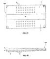
- FIG. 4Ais a side elevation of a stress balanced semiconductor device assembly according to the present invention.
- FIG. 4Bis a plan view of the stress balanced semiconductor device assembly of FIG. 4A;
- FIG. 4Cis a side sectional view of a wire bonded BOC stress balanced semiconductor device assembly having an external configuration in accordance with FIGS. 4A and 4B;
- FIG. 4Dis a side sectional view of a wire bonded COB stress balanced semiconductor device assembly having an external configuration in accordance with FIGS. 4A and 4B;
- FIG. 4Eis a side sectional view of a flip-chip semiconductor device assembly on an interposer substrate having an external configuration in accordance with FIGS. 4A and 4B;
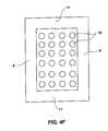
- FIG. 4Fis a plan view of another external configuration of a stress balanced semiconductor device assembly suitable for use with the COB semiconductor device assemblies of FIGS. 4D and 4E;
- FIG. 5is a schematic elevation of a memory module including a plurality of stress balanced semiconductor device assemblies according to the present invention.
- FIG. 6is a computer system including at least one stress balanced semiconductor device assembly according to the present invention.
- At least one semiconductor die 2is mounted by conventional methods such as adhesive or other bonding agent (and, in some instances, by a flip-chip connection) to form either a chip-on-board (COB) or board-on-chip (BOC) assembly with substrate 4 .
- Substrate 4may be a printed circuit board formed, for example, of BT resin or comprising an FR-4 or FR-5 laminate, a ceramic substrate, a silicon substrate, a flexible circuit board, or any other type of rigid or flexible circuit board material known to one of ordinary skill in the art.
- Semiconductor die 2is encapsulated with a material as shown by die encapsulation region 8 on a first side of substrate 4 .
- Discrete conductive elements 12are provided on the side of substrate 4 opposite semiconductor die 2 .
- Discrete conductive elements 12may be arranged in a ball grid array or other suitable configuration for mechanically and electrically connecting the semiconductor device assembly to higher-level packaging.
- an assembly 400is used where a stem member 9 and at least one branch member 11 extending from stem member 9 are provided adjacent to discrete conductive elements 12 .
- Stem member 9extends in a longitudinal direction and branch member 11 extends in a transverse direction.
- FIG. 4Bshows a preferred geometry where stem member 9 extends longitudinally between two portions of an array of discrete conductive elements 12 and two branch members 11 extend in a transverse direction at each end of the array of discrete conductive elements 12 .
- stem member 9 and branch member 11may be substantially perpendicular to each other.
- stem member 9 and branch member 11are formed at the same time and form an integral structure.
- a BOC assembly 400 Cis used where semiconductor die 2 is electrically connected to substrate 4 using bond wires 6 .
- Bond wires 6are extended between bond pads 3 of semiconductor die 2 and terminal pads 5 of substrate 4 through slot 7 using conventional wire bonding techniques known to one skilled in the art.
- substrate 4may be a printed circuit board, flexible circuit board, or any other type of circuit board known to one skilled in the art.
- Discrete conductive elements 12are provided on the side of substrate 4 opposite semiconductor die 2 . Discrete conductive elements 12 may comprise an array such as a BGA.
- Wires 6are encapsulated by a wire bond cap 10 which, according to the present invention, also comprises a longitudinally extending stem member 9 along substrate 4 adjacent to and between two portions of the array of discrete conductive elements 12 . At least one branch member 11 may extend in a direction substantially transverse to stem member 9 and laterally across substrate 4 . Two branch members 11 may respectively lie preferably on opposing sides of discrete conductive elements 12 . In this embodiment, combined wire bond cap 10 and stem member 9 and contiguous branch members 11 are preferably formed at the same time and simultaneously with formation of die encapsulation region 8 to form an integral assembly.
- wire bond cap 10 /stem member 9 , branch members 11 and die encapsulation region 8be formed in a transfer molding process wherein a molten, silicon-filled thermoplastic polymer dielectric mold compound is molded about the BOC assembly in a transfer mold.
- Such a transfer moldmay comprise two mold segments, one configured with a mold cavity to form die encapsulation region 8 and the opposing one configured to define wire bond cap 10 /stem member 9 and branch members 11 . Both mold segments will, of course, sealingly engage a surface of substrate 4 to preclude mold compound bleeding onto unwanted areas of substrate 4 . It should be noted that the embodiments shown in FIGS. 4 A- 4 F have the advantage of not having to introduce additional process steps since bond wires 6 are typically encapsulated in conventional BOC wire bonded assemblies (i.e., a wire bond cap) simultaneously with die encapsulation region 8 and, in the other embodiments, an appropriate mold segment may be configured and employed in the molding process already in use.
- the modification of an existing mold segment defining the wire bond cap 10 /longitudinal stem member 9 in the embodiment of FIG. 4C to include mold cavity portions to define laterally extending branch members 11 configured as shown in FIG. 4Bmay be easily effected using, for example, a milling machine or electrodischarge machining (EDM), among other techniques.
- EDMelectrodischarge machining
- additional runners and ventsmay be added to the mold segment as desired or required. Accordingly, once the mold segment is so modified, the only additional cost in the BOC assembly encapsulation process is the minimal cost of the additional mold compound used to define the branch members 11 .
- a transfer molding moldis normally configured for molding of a large number of semiconductor device assemblies and the mold segments used to define wire bond cap 10 /stem member 9 for each of such assemblies may be modified to the configuration of the present invention.
- FIG. 4Ddepicts a COB assembly 400 D in accordance with the present invention, wherein semiconductor die 2 is back-bonded to carrier substrate 4 , and die encapsulation region 8 extends over bond wires 6 facing away from substrate 4 .
- Discrete conductive elements 12are operably coupled to bond wires 6 through vias and, if desired or required, a redistribution layer (RDL) extending over a surface of substrate 4 or redistribution traces extending therewithin.
- RDLredistribution layer
- Longitudinal stem member 9 and branch members 11are arranged as depicted in FIG. 4B, although this arrangement is not required. For example, stem member 9 may be eliminated and one or more branch members 11 used alone. Alternatively, as shown in FIG.
- two longitudinal stem members 9may be placed along parallel, opposing edges of substrate 4 , with branch members 11 placed along parallel, opposing edges of substrate 4 oriented perpendicular to the other two edges, stem members 9 and branch members 11 framing an array wherein a BGA of discrete conductive elements 12 may be placed.
- a mold segmentconfigured to achieve the foregoing stem member and branch member configuration would be placed against the side of substrate 4 opposite to semiconductor die 2 .
- FIG. 4Eshows a COB assembly 400 E using a flip-chip type semiconductor die 2 having solder bumps or other discrete conductive elements 14 extending from an active surface of semiconductor die 2 to mechanically and electrically connect semiconductor die 2 to substrate 4 .
- the BGA side of substrate 4may be configured as depicted in FIG. 4B or 4 F.
- the resulting neutral axis of the semiconductor packageis preferably located to be at least near, if not coincident with, the center of substrate 4 . That is to say, while the substrate extends primarily in the X-Y plane, it also has a depth or thickness transverse to the X-Y plane which is commonly referenced as the “Z” dimension of the substrate.
- the present inventiondesirably places the neutral axis, or location wherein internal bending stresses are negligible to nonexistent, within the center of the substrate.
- This designhas the advantage of substantially lowering or even eliminating tensile stresses near the substrate, reducing the tendency of the semiconductor package to bow, reducing the tendency of cracking in stem member 9 , and eliminating or reducing the tendency of the assembly to exhibit the aforementioned structural problems.
- Stem member or members 9 and branch member or members 11may also provide additional structural support for the semiconductor package.
- die encapsulation region 8 , stem member 9 , and branch member or members 11may be formed from materials known in the art and the encapsulant material used may be the same for both sides of substrate 4 .
- polymerssuch as epoxies, silicones, silicone-carbon resins (SYNCARTM), polyimides, or polyurethanes may be used.
- Composite materialssuch as reinforced polymers may also be selected for die encapsulation region 8 , stem member 9 , and branch member 11 .
- Die encapsulation region 8 , stem member 9 , and branch member or members 11may be formed from molding techniques known in the art other than transfer molding, including, for example, pot molding and injection molding. Other methods and materials to produce die encapsulation region 8 , stem member 9 , and branch member 11 will be readily apparent to those of ordinary skill in the art.
- the present inventionprovides, through the presence of at least one stem member and at least one branch member, a stabilizing structure for the BGA and a standoff for discrete conductive elements 12 thereof.
- a memory device or module 500which incorporates a plurality of semiconductor dice 2 packaged according to the present invention.
- the memory device 500includes a printed circuit board 16 to which the one or more packaged semiconductor dice 2 may be mechanically and electrically operably coupled therewith to form a memory module.
- a plurality of electrical edge connectors 18may be formed on the printed circuit board 16 to provide input and output connections from an external device, such as, for example, a motherboard of a computer, to the one or more semiconductor dice 2 .
- a computer system 600which includes a printed circuit board 18 such as, for example, a motherboard.
- the printed circuit board 18may be operably coupled to at least one processor 20 , such as, for example, a central processing unit, (CPU) and at least one memory device 500 .
- the memory device 500may include one or more semiconductor dice 2 packaged as described above in the present invention.
- the printed circuit board 18is operably coupled with at least one input device 22 such as, for example, a keyboard, a mouse, a sensor or another other computing device.
- the printed circuit board 18is also operably coupled with at least one output device 24 such as, for example, a printer, a monitor, an actuator or another computing device.
Landscapes
- Engineering & Computer Science (AREA)
- Microelectronics & Electronic Packaging (AREA)
- Physics & Mathematics (AREA)
- Condensed Matter Physics & Semiconductors (AREA)
- General Physics & Mathematics (AREA)
- Computer Hardware Design (AREA)
- Power Engineering (AREA)
- Manufacturing & Machinery (AREA)
- Structures Or Materials For Encapsulating Or Coating Semiconductor Devices Or Solid State Devices (AREA)
- Encapsulation Of And Coatings For Semiconductor Or Solid State Devices (AREA)
Abstract
Description
- This application is a divisional of application Ser. No. 10/227,329, filed Aug. 23, 2002, pending.[0001]
- 1. Field of the Invention[0002]
- The present invention relates to the packaging of electronic components such as integrated circuits or other electronic devices. In particular, this invention relates to an improved semiconductor device package wherein at least one semiconductor die is encapsulated on a substrate and another volume of encapsulant material is added to the opposing side of the substrate in a configuration to assist in control of the stresses in the package.[0003]
- 2. State of the Art[0004]
- Conventionally, semiconductor dice have been packaged in plastic or, less commonly, in ceramic packages. Packages may support, protect, and dissipate heat from semiconductor dice. Packages may also provide external connective elements for providing power and signal distribution to and from semiconductor dice, as well as for facilitating electrical testing, such as burn-in testing and circuit evaluation, of semiconductor dice prior to or after assembly thereof with higher-level components, such as carrier substrates or circuit boards.[0005]
- FIG. 1A schematically illustrates a section of a conventional board-on-chip (BOC)[0006]
semiconductor device assembly 100A with electrical contacts which conventionally comprise a ball grid array (BGA) of discreteconductive elements 12 such as solder balls. FIG. 1A showssubstrate 4, typically a printed circuit board, mounted to semiconductor die2. Semiconductor die2 is placed in electrical communication withsubstrate 4 bybond wires 6 extending betweenbond pads 3 of semiconductor die2 andterminal pads 5 throughslot 7 insubstrate 4 using conventional wire bonding techniques. Both semiconductor die2 andbond wires 6 are encapsulated in a transfer molded, filled polymer volume of encapsulant material shown bydie encapsulation region 8 andwire bond cap 10. FIG. 1B illustrates a side view and FIG. 1C illustrates a plan view of thesemiconductor device assembly 100A of FIG. 1A. - FIG. 2A schematically illustrates a conventional chip-on-board (COB)[0007]
assembly 200A fabricated using conventional wire bonding techniques. FIG. 2B shows a flip-chip configuredsemiconductor device assembly 200B that utilizes solder bumps14 instead of wire bonds to electrically connect semiconductor die2 tosubstrate 4. - A semiconductor die, the encapsulation material, the adhesives or other bonding agents used to connect the semiconductor die to the substrate, the substrate, and the electrical connection mechanisms between the semiconductor die and the substrate of a semiconductor device assembly are usually each made from a different material or combination of materials. These different materials usually have different thermomechanical properties due to differing coefficients of thermal expansion (CTE), which differences result in stresses developing during manufacture or use of the semiconductor device assembly, the latter due to thermal cycling. Several problems can result during manufacture and use of semiconductor device assemblies due to the development of these thermomechanical-related stresses. For instance, bowing of the semiconductor device assembly can occur due to internal bending stresses, causing cracking in the encapsulant materials and subjecting components to environmental degradation, debonding of the semiconductor die from the substrate, solder joint failure, or cracking in the substrate itself. Even if minimal bowing is manifested initially, residual tensile stresses can still be present, eventually resulting in the same problems after a period of time due to thermal cycling-induced fatigue experienced during normal operation.[0008]
- Residual tensile stresses develop during manufacture from the aforementioned mismatch of material CTEs, as well as from shrinkage of the encapsulation material during curing and hardening thereof. FIG. 3 shows an exaggerated view of bowing in a wire bonded[0009]
BOC assembly 100A as previously depicted in FIG. 1A due to the thermomechanical stresses. The bowing occurs in significant part due to the imbalance of the volume of encapsulant material between the two opposing sides ofsubstrate 4. As shown in FIG. 3, there is significantly more encapsulant material volume present in dieencapsulation region 8 than inwire bond cap 10. Further, dieencapsulation region 8 extends completely acrosssubstrate 4, whilewire bond cap 10 runs primarily longitudinally oversubstrate 4, extending laterally only a sufficient distance to coverbond wires 6 andslot 7. The resulting predominant tensile stress developed nearsubstrate 4 and on one side thereof due to shrinkage of the substantially different volumes and extents of the encapsulant material applied to the opposing sides ofsubstrate 4 can cause significant problems with respect to package integrity. One particularly notable problem is cracking inwire bond cap 10, which exposes the wires to environmental degradation and may itself cause breakage of the thin,delicate bond wires 6. - The prior art has attempted to address the issues of undesirable stresses in semiconductor packaging. For example, U.S. Pat. No. 5,627,407 to Suhir et al. purportedly solves the problem of unwanted thermomechanical stresses by using a thin “surrogate layer” on the entire substrate side opposite the encapsulated semiconductor die. However, this method utilizes significantly more material in the surrogate layer than may be needed and involves the use of a different material than the encapsulant. Also, by covering an entire side of the substrate with the surrogate layer, it is difficult, if not impossible, to place discrete conductive elements, such as a BGA, on the substrate side bearing the surrogate layer. Further, adding this surrogate layer may be required to be performed as an additional process step. Little guidance is provided as to how the encapsulant and the surrogate layer might be applied concurrently, as is indicated by Suhir as being a desirable approach. In addition, placement of a surrogate layer proximate each substrate and prior to encapsulation will itself require additional cost and alignment considerations.[0010]
- U.S. Pat. No. 6,294,831 to Shishido et al. attempts to reduce bowing in a flip-chip type semiconductor device assembly by bonding a structure over the back side of a flip-chip configured semiconductor die and on the opposing side of the semiconductor die to an interposer substrate to which the semiconductor die is mechanically secured and electrically connected, the structure having a CTE similar to that of the substrate.[0011]
- U.S. Pat. No. 6,291,899 to Wensel et al. addresses bowing in a COB BGA semiconductor device assembly by applying a so-called stabilizing plate to a side of the substrate opposite that to which the semiconductor die is back side-attached and wire bonded. The stabilizing plate is formed of a rigid material different from that used to encapsulate the semiconductor die and is applied before the encapsulant is applied over the semiconductor die. Placement of the stabilizing plate on the side of the substrate carrying the discrete conductive elements of the BGA also requires fairly precise alignment of the stabilizing plate during placement.[0012]
- Other U.S. Patents have addressed the issue of stresses in semiconductor packages but only with regard to bowing in lead frame assemblies. For example, U.S. Pat. No. 6,384,487 to Smith and U.S. Pat. No. 6,258,624 to Corisis attempt to equalize the volume of encapsulant material on both sides of a lead frame to minimize bowing. U.S. Pat. No. 6,316,829 to Boon et al. attempts to solve the same problem, but by molding grooves and ridges in an encapsulated lead frame.[0013]
- While the prior art has attempted to address bowing and other stress-related problems in semiconductor device assemblies, a need exists for a semiconductor device assembly of a design whereby the stresses in the assembly can be controlled effectively while not requiring added process steps or the use of substantial additional materials, expensive materials or complex structural configurations, each of which increase fabrication cost. Further, it would be desirable to provide a semiconductor device assembly design which easily accommodates the use of a BGA for connection to higher-level packaging.[0014]
- The present invention provides a structural configuration which substantially balances stresses in semiconductor device assemblies through selective placement of encapsulant material on opposing sides of a substrate. The semiconductor device assembly includes at least one semiconductor die mounted to a substrate in either a board-on-chip (BOC) or chip-on-board (COB) configuration. Flip-chip, wire bonding, or any other technique known in the art may be used to electrically connect the semiconductor die to the substrate. The semiconductor die is attached and electrically connected to one side of a substrate with discrete conductive elements such as a ball grid array (BGA) on the opposing side of the substrate.[0015]
- In a broad embodiment, at least one stem member and at least one transversely extending branch member may be placed on the side of a carrier substrate such as an interposer substrate opposite the side on which a semiconductor die and die encapsulation region extending over them are placed. The combined volumes of the stem and branch member may be substantially equal to the volume of the die encapsulation region.[0016]
- One exemplary embodiment of the present invention comprises a wire bonded BOC semiconductor device assembly where the wire bonds extending between the bond pads of the semiconductor die and terminal pads of the substrate are encapsulated with a longitudinally extending wire bond cap in a conventional manner with at least one laterally extending branch member of encapsulant material formed over the same side of the substrate as the wire bond cap. The wire bond cap and at least one branch member may be formed simultaneously with an encapsulation region formed over the semiconductor die.[0017]
- Another exemplary embodiment of the present invention comprises a wire bonded COB assembly wherein the semiconductor die and wire bonds are encapsulated on one side of the substrate and at least one additional longitudinally extending stem member having at least one laterally extending branch member of encapsulant material may be formed on the opposing side of the substrate and simultaneously with encapsulation of the semiconductor die and wire bonds.[0018]
- Yet another exemplary embodiment of the present invention comprises a semiconductor device package wherein a flip-chip configured semiconductor die is attached and electrically connected to a substrate. The semiconductor die may be encapsulated on one side of the substrate simultaneously with application of encapsulant material to the opposing side of the substrate in a configuration providing at least one longitudinal member and at least one laterally extending member.[0019]
- The present invention offers the advantage, among others, of reducing internal bending stresses on an encapsulated semiconductor device assembly by moving the neutral axis, where such bending stresses are slight to nonexistent, closer to or even within the center of the substrate. Further, the stress-balancing structures of the present invention are formed using an insubstantial volume of additional encapsulant material and simultaneously with molding of an encapsulant envelope over the semiconductor die and, if applicable, a wire bond cap.[0020]
- The present invention also encompasses a method of making the above semiconductor packages and a method of modifying a mold segment for use in the method.[0021]
- In the drawings, which illustrate what is currently considered to be the best mode for carrying out the invention and in which like elements and features are identified by like reference numerals:[0022]
- FIG. 1A is a schematic sectional view of a conventional BOC semiconductor device assembly utilizing wire bonding;[0023]
- FIG. 1B is a side elevation of a conventional BOC semiconductor device assembly utilizing wire bonding;[0024]
- FIG. 1C is a plan view of the conventional BOC semiconductor device assembly of FIG. 1B;[0025]
- FIG. 2A is a schematic sectional view of a conventional COB semiconductor device assembly utilizing wire bonding;[0026]
- FIG. 2B is a schematic sectional view of a conventional COB semiconductor device utilizing a flip-chip configured die;[0027]
- FIG. 3 is a schematic sectional view of the semiconductor device assembly of FIG. 1A bowed under stress;[0028]
- FIG. 4A is a side elevation of a stress balanced semiconductor device assembly according to the present invention;[0029]
- FIG. 4B is a plan view of the stress balanced semiconductor device assembly of FIG. 4A;[0030]
- FIG. 4C is a side sectional view of a wire bonded BOC stress balanced semiconductor device assembly having an external configuration in accordance with FIGS. 4A and 4B;[0031]
- FIG. 4D is a side sectional view of a wire bonded COB stress balanced semiconductor device assembly having an external configuration in accordance with FIGS. 4A and 4B;[0032]
- FIG. 4E is a side sectional view of a flip-chip semiconductor device assembly on an interposer substrate having an external configuration in accordance with FIGS. 4A and 4B;[0033]
- FIG. 4F is a plan view of another external configuration of a stress balanced semiconductor device assembly suitable for use with the COB semiconductor device assemblies of FIGS. 4D and 4E;[0034]
- FIG. 5 is a schematic elevation of a memory module including a plurality of stress balanced semiconductor device assemblies according to the present invention; and[0035]
- FIG. 6 is a computer system including at least one stress balanced semiconductor device assembly according to the present invention.[0036]
- Referring to FIGS.[0037]4A-E, at least one semiconductor die2 is mounted by conventional methods such as adhesive or other bonding agent (and, in some instances, by a flip-chip connection) to form either a chip-on-board (COB) or board-on-chip (BOC) assembly with
substrate 4.Substrate 4 may be a printed circuit board formed, for example, of BT resin or comprising an FR-4 or FR-5 laminate, a ceramic substrate, a silicon substrate, a flexible circuit board, or any other type of rigid or flexible circuit board material known to one of ordinary skill in the art. Semiconductor die2 is encapsulated with a material as shown bydie encapsulation region 8 on a first side ofsubstrate 4. Discreteconductive elements 12 are provided on the side ofsubstrate 4 opposite semiconductor die2. Discreteconductive elements 12 may be arranged in a ball grid array or other suitable configuration for mechanically and electrically connecting the semiconductor device assembly to higher-level packaging. - In one embodiment, as shown in FIGS. 4A and 4B, an[0038]
assembly 400 is used where astem member 9 and at least onebranch member 11 extending fromstem member 9 are provided adjacent to discreteconductive elements 12.Stem member 9 extends in a longitudinal direction andbranch member 11 extends in a transverse direction. FIG. 4B shows a preferred geometry wherestem member 9 extends longitudinally between two portions of an array of discreteconductive elements 12 and twobranch members 11 extend in a transverse direction at each end of the array of discreteconductive elements 12. Further and as shown,stem member 9 andbranch member 11 may be substantially perpendicular to each other. In one embodiment,stem member 9 andbranch member 11 are formed at the same time and form an integral structure. - In an exemplary embodiment as shown in FIG. 4C employing the external configuration shown in FIGS. 4A and 4B, a[0039]
BOC assembly 400C is used where semiconductor die2 is electrically connected tosubstrate 4 usingbond wires 6.Bond wires 6 are extended betweenbond pads 3 of semiconductor die2 andterminal pads 5 ofsubstrate 4 throughslot 7 using conventional wire bonding techniques known to one skilled in the art. As in the other exemplary embodiments,substrate 4 may be a printed circuit board, flexible circuit board, or any other type of circuit board known to one skilled in the art. Discreteconductive elements 12 are provided on the side ofsubstrate 4 opposite semiconductor die2. Discreteconductive elements 12 may comprise an array such as a BGA. Semiconductor die2 is encapsulated bydie encapsulation region 8.Bond wires 6 are encapsulated by awire bond cap 10 which, according to the present invention, also comprises a longitudinally extendingstem member 9 alongsubstrate 4 adjacent to and between two portions of the array of discreteconductive elements 12. At least onebranch member 11 may extend in a direction substantially transverse to stemmember 9 and laterally acrosssubstrate 4. Twobranch members 11 may respectively lie preferably on opposing sides of discreteconductive elements 12. In this embodiment, combinedwire bond cap 10 and stemmember 9 andcontiguous branch members 11 are preferably formed at the same time and simultaneously with formation ofdie encapsulation region 8 to form an integral assembly. It is also currently preferred thatwire bond cap 10/stem member 9,branch members 11 and dieencapsulation region 8 be formed in a transfer molding process wherein a molten, silicon-filled thermoplastic polymer dielectric mold compound is molded about the BOC assembly in a transfer mold. - Such a transfer mold may comprise two mold segments, one configured with a mold cavity to form[0040]
die encapsulation region 8 and the opposing one configured to definewire bond cap 10/stem member 9 andbranch members 11. Both mold segments will, of course, sealingly engage a surface ofsubstrate 4 to preclude mold compound bleeding onto unwanted areas ofsubstrate 4. It should be noted that the embodiments shown in FIGS.4A-4F have the advantage of not having to introduce additional process steps sincebond wires 6 are typically encapsulated in conventional BOC wire bonded assemblies (i.e., a wire bond cap) simultaneously withdie encapsulation region 8 and, in the other embodiments, an appropriate mold segment may be configured and employed in the molding process already in use. - The modification of an existing mold segment defining the[0041]
wire bond cap 10/longitudinal stem member 9 in the embodiment of FIG. 4C to include mold cavity portions to define laterally extendingbranch members 11 configured as shown in FIG. 4B may be easily effected using, for example, a milling machine or electrodischarge machining (EDM), among other techniques. Of course, additional runners and vents may be added to the mold segment as desired or required. Accordingly, once the mold segment is so modified, the only additional cost in the BOC assembly encapsulation process is the minimal cost of the additional mold compound used to define thebranch members 11. Of course, a transfer molding mold is normally configured for molding of a large number of semiconductor device assemblies and the mold segments used to definewire bond cap 10/stem member 9 for each of such assemblies may be modified to the configuration of the present invention. - FIG. 4D depicts a[0042]
COB assembly 400D in accordance with the present invention, wherein semiconductor die2 is back-bonded tocarrier substrate 4, and dieencapsulation region 8 extends overbond wires 6 facing away fromsubstrate 4. Discreteconductive elements 12 are operably coupled tobond wires 6 through vias and, if desired or required, a redistribution layer (RDL) extending over a surface ofsubstrate 4 or redistribution traces extending therewithin.Longitudinal stem member 9 andbranch members 11 are arranged as depicted in FIG. 4B, although this arrangement is not required. For example,stem member 9 may be eliminated and one ormore branch members 11 used alone. Alternatively, as shown in FIG. 4F, twolongitudinal stem members 9 may be placed along parallel, opposing edges ofsubstrate 4, withbranch members 11 placed along parallel, opposing edges ofsubstrate 4 oriented perpendicular to the other two edges,stem members 9 andbranch members 11 framing an array wherein a BGA of discreteconductive elements 12 may be placed. Thus, a mold segment configured to achieve the foregoing stem member and branch member configuration would be placed against the side ofsubstrate 4 opposite to semiconductor die2. - FIG. 4E shows a[0043]
COB assembly 400E using a flip-chip type semiconductor die2 having solder bumps or other discreteconductive elements 14 extending from an active surface of semiconductor die2 to mechanically and electrically connect semiconductor die2 tosubstrate 4. As with the other embodiments, the BGA side ofsubstrate 4 may be configured as depicted in FIG. 4B or4F. - In all embodiments shown in FIGS.[0044]4A-4F, the resulting neutral axis of the semiconductor package is preferably located to be at least near, if not coincident with, the center of
substrate 4. That is to say, while the substrate extends primarily in the X-Y plane, it also has a depth or thickness transverse to the X-Y plane which is commonly referenced as the “Z” dimension of the substrate. Thus, the present invention desirably places the neutral axis, or location wherein internal bending stresses are negligible to nonexistent, within the center of the substrate. This design has the advantage of substantially lowering or even eliminating tensile stresses near the substrate, reducing the tendency of the semiconductor package to bow, reducing the tendency of cracking instem member 9, and eliminating or reducing the tendency of the assembly to exhibit the aforementioned structural problems. Stem member ormembers 9 and branch member ormembers 11 may also provide additional structural support for the semiconductor package. - Further, in all embodiments shown by FIGS.[0045]4A-F, die
encapsulation region 8,stem member 9, and branch member ormembers 11 may be formed from materials known in the art and the encapsulant material used may be the same for both sides ofsubstrate 4. For example, polymers such as epoxies, silicones, silicone-carbon resins (SYNCAR™), polyimides, or polyurethanes may be used. Composite materials such as reinforced polymers may also be selected fordie encapsulation region 8,stem member 9, andbranch member 11. Dieencapsulation region 8,stem member 9, and branch member ormembers 11 may be formed from molding techniques known in the art other than transfer molding, including, for example, pot molding and injection molding. Other methods and materials to producedie encapsulation region 8,stem member 9, andbranch member 11 will be readily apparent to those of ordinary skill in the art. - It will also be appreciated that the present invention provides, through the presence of at least one stem member and at least one branch member, a stabilizing structure for the BGA and a standoff for discrete[0046]
conductive elements 12 thereof. - Referring now to FIG. 5, a memory device or[0047]
module 500 is shown which incorporates a plurality ofsemiconductor dice 2 packaged according to the present invention. Thememory device 500 includes a printedcircuit board 16 to which the one or more packagedsemiconductor dice 2 may be mechanically and electrically operably coupled therewith to form a memory module. A plurality ofelectrical edge connectors 18 may be formed on the printedcircuit board 16 to provide input and output connections from an external device, such as, for example, a motherboard of a computer, to the one ormore semiconductor dice 2. - Referring now to FIG. 6, a[0048]
computer system 600 is shown which includes a printedcircuit board 18 such as, for example, a motherboard. The printedcircuit board 18 may be operably coupled to at least oneprocessor 20, such as, for example, a central processing unit, (CPU) and at least onememory device 500. Thememory device 500 may include one ormore semiconductor dice 2 packaged as described above in the present invention. The printedcircuit board 18 is operably coupled with at least oneinput device 22 such as, for example, a keyboard, a mouse, a sensor or another other computing device. The printedcircuit board 18 is also operably coupled with at least oneoutput device 24 such as, for example, a printer, a monitor, an actuator or another computing device. - Although the foregoing description contains many specifics, these are not to be construed as limiting the scope of the present invention, but merely as providing certain exemplary embodiments. Similarly, other embodiments of the invention may be devised which do not depart from the spirit or scope of the present invention. The scope of the invention is, therefore, indicated and limited only by the appended claims and their legal equivalents, rather than by the foregoing description. All additions, deletions, and modifications to the invention, as disclosed herein, which fall within the meaning and scope of the claims are encompassed by the present invention.[0049]
Claims (9)
Priority Applications (2)
| Application Number | Priority Date | Filing Date | Title |
|---|---|---|---|
| US10/636,332US6855574B2 (en) | 2002-08-23 | 2003-08-06 | Stress balanced semiconductor packages, method of fabrication and modified mold segment |
| US10/921,650US7084489B2 (en) | 2002-08-23 | 2004-08-18 | Computer system including at least one stress balanced semiconductor package |
Applications Claiming Priority (2)
| Application Number | Priority Date | Filing Date | Title |
|---|---|---|---|
| US10/227,329US6696748B1 (en) | 2002-08-23 | 2002-08-23 | Stress balanced semiconductor packages, method of fabrication and modified mold segment |
| US10/636,332US6855574B2 (en) | 2002-08-23 | 2003-08-06 | Stress balanced semiconductor packages, method of fabrication and modified mold segment |
Related Parent Applications (1)
| Application Number | Title | Priority Date | Filing Date |
|---|---|---|---|
| US10/227,329DivisionUS6696748B1 (en) | 2002-08-23 | 2002-08-23 | Stress balanced semiconductor packages, method of fabrication and modified mold segment |
Related Child Applications (1)
| Application Number | Title | Priority Date | Filing Date |
|---|---|---|---|
| US10/921,650ContinuationUS7084489B2 (en) | 2002-08-23 | 2004-08-18 | Computer system including at least one stress balanced semiconductor package |
Publications (2)
| Publication Number | Publication Date |
|---|---|
| US20040038457A1true US20040038457A1 (en) | 2004-02-26 |
| US6855574B2 US6855574B2 (en) | 2005-02-15 |
Family
ID=31495325
Family Applications (3)
| Application Number | Title | Priority Date | Filing Date |
|---|---|---|---|
| US10/227,329Expired - LifetimeUS6696748B1 (en) | 2002-08-23 | 2002-08-23 | Stress balanced semiconductor packages, method of fabrication and modified mold segment |
| US10/636,332Expired - LifetimeUS6855574B2 (en) | 2002-08-23 | 2003-08-06 | Stress balanced semiconductor packages, method of fabrication and modified mold segment |
| US10/921,650Expired - Fee RelatedUS7084489B2 (en) | 2002-08-23 | 2004-08-18 | Computer system including at least one stress balanced semiconductor package |
Family Applications Before (1)
| Application Number | Title | Priority Date | Filing Date |
|---|---|---|---|
| US10/227,329Expired - LifetimeUS6696748B1 (en) | 2002-08-23 | 2002-08-23 | Stress balanced semiconductor packages, method of fabrication and modified mold segment |
Family Applications After (1)
| Application Number | Title | Priority Date | Filing Date |
|---|---|---|---|
| US10/921,650Expired - Fee RelatedUS7084489B2 (en) | 2002-08-23 | 2004-08-18 | Computer system including at least one stress balanced semiconductor package |
Country Status (1)
| Country | Link |
|---|---|
| US (3) | US6696748B1 (en) |
Cited By (3)
| Publication number | Priority date | Publication date | Assignee | Title |
|---|---|---|---|---|
| DE102004056534A1 (en)* | 2004-11-23 | 2006-06-01 | Infineon Technologies Ag | Semiconductor component with a semiconductor chip and with external contacts and method for producing the same |
| US20080054494A1 (en)* | 2006-09-01 | 2008-03-06 | Powertech Technology Inc. | IC package |
| US20090039529A1 (en)* | 2007-08-08 | 2009-02-12 | Sebastian Mueller | Integrated Circuit Having a Plurality of Connection Pads and Integrated Circuit Package |
Families Citing this family (13)
| Publication number | Priority date | Publication date | Assignee | Title |
|---|---|---|---|---|
| US7265994B2 (en)* | 2003-01-31 | 2007-09-04 | Freescale Semiconductor, Inc. | Underfill film for printed wiring assemblies |
| US7205656B2 (en)* | 2005-02-22 | 2007-04-17 | Micron Technology, Inc. | Stacked device package for peripheral and center device pad layout device |
| US7408246B2 (en)* | 2005-03-31 | 2008-08-05 | Agere Systems, Inc. | Controlling warping in integrated circuit devices |
| TWI269420B (en)* | 2005-05-03 | 2006-12-21 | Megica Corp | Stacked chip package and process thereof |
| US7573125B2 (en)* | 2005-06-14 | 2009-08-11 | Micron Technology, Inc. | Methods for reducing stress in microelectronic devices and microelectronic devices formed using such methods |
| US7416943B2 (en)* | 2005-09-01 | 2008-08-26 | Micron Technology, Inc. | Peripheral gate stacks and recessed array gates |
| JP4386453B2 (en)* | 2006-05-31 | 2009-12-16 | 信越化学工業株式会社 | Resin-sealed semiconductor device |
| US8198735B2 (en) | 2006-12-31 | 2012-06-12 | Stats Chippac Ltd. | Integrated circuit package with molded cavity |
| US8258015B2 (en)* | 2008-02-22 | 2012-09-04 | Stats Chippac Ltd. | Integrated circuit package system with penetrable film adhesive |
| US8304869B2 (en)* | 2008-08-01 | 2012-11-06 | Stats Chippac Ltd. | Fan-in interposer on lead frame for an integrated circuit package on package system |
| US8718550B2 (en) | 2011-09-28 | 2014-05-06 | Broadcom Corporation | Interposer package structure for wireless communication element, thermal enhancement, and EMI shielding |
| US11551986B2 (en)* | 2020-04-02 | 2023-01-10 | Texas Instruments Incorporated | Shape memory polymer for use in semiconductor device fabrication |
| US12389693B2 (en) | 2022-05-23 | 2025-08-12 | Semiconductor Components Industries, Llc | Optoelectronic device having a modular package |
Citations (10)
| Publication number | Priority date | Publication date | Assignee | Title |
|---|---|---|---|---|
| US4887148A (en)* | 1988-07-15 | 1989-12-12 | Advanced Micro Devices, Inc. | Pin grid array package structure |
| US5627407A (en)* | 1995-04-28 | 1997-05-06 | Lucent Technologies Inc. | Electronic package with reduced bending stress |
| US5834848A (en)* | 1996-12-03 | 1998-11-10 | Kabushiki Kaisha Toshiba | Electronic device and semiconductor package |
| US5901041A (en)* | 1997-12-02 | 1999-05-04 | Northern Telecom Limited | Flexible integrated circuit package |
| US5900675A (en)* | 1997-04-21 | 1999-05-04 | International Business Machines Corporation | Organic controlled collapse chip connector (C4) ball grid array (BGA) chip carrier with dual thermal expansion rates |
| US6258624B1 (en)* | 2000-01-10 | 2001-07-10 | Micron Technology, Inc. | Semiconductor package having downset leadframe for reducing package bow |
| US6291899B1 (en)* | 1999-02-16 | 2001-09-18 | Micron Technology, Inc. | Method and apparatus for reducing BGA warpage caused by encapsulation |
| US6294831B1 (en)* | 1998-11-05 | 2001-09-25 | International Business Machines Corporation | Electronic package with bonded structure and method of making |
| US6316829B1 (en)* | 1998-06-18 | 2001-11-13 | Texas Instruments Incorporated | Reinforced semiconductor package |
| US6384487B1 (en)* | 1999-12-06 | 2002-05-07 | Micron Technology, Inc. | Bow resistant plastic semiconductor package and method of fabrication |
Family Cites Families (5)
| Publication number | Priority date | Publication date | Assignee | Title |
|---|---|---|---|---|
| US6084297A (en)* | 1998-09-03 | 2000-07-04 | Micron Technology, Inc. | Cavity ball grid array apparatus |
| US6522018B1 (en)* | 2000-05-16 | 2003-02-18 | Micron Technology, Inc. | Ball grid array chip packages having improved testing and stacking characteristics |
| US6717245B1 (en)* | 2000-06-02 | 2004-04-06 | Micron Technology, Inc. | Chip scale packages performed by wafer level processing |
| US6528408B2 (en)* | 2001-05-21 | 2003-03-04 | Micron Technology, Inc. | Method for bumped die and wire bonded board-on-chip package |
| US6800930B2 (en)* | 2002-07-31 | 2004-10-05 | Micron Technology, Inc. | Semiconductor dice having back side redistribution layer accessed using through-silicon vias, and assemblies |
- 2002
- 2002-08-23USUS10/227,329patent/US6696748B1/ennot_activeExpired - Lifetime
- 2003
- 2003-08-06USUS10/636,332patent/US6855574B2/ennot_activeExpired - Lifetime
- 2004
- 2004-08-18USUS10/921,650patent/US7084489B2/ennot_activeExpired - Fee Related
Patent Citations (10)
| Publication number | Priority date | Publication date | Assignee | Title |
|---|---|---|---|---|
| US4887148A (en)* | 1988-07-15 | 1989-12-12 | Advanced Micro Devices, Inc. | Pin grid array package structure |
| US5627407A (en)* | 1995-04-28 | 1997-05-06 | Lucent Technologies Inc. | Electronic package with reduced bending stress |
| US5834848A (en)* | 1996-12-03 | 1998-11-10 | Kabushiki Kaisha Toshiba | Electronic device and semiconductor package |
| US5900675A (en)* | 1997-04-21 | 1999-05-04 | International Business Machines Corporation | Organic controlled collapse chip connector (C4) ball grid array (BGA) chip carrier with dual thermal expansion rates |
| US5901041A (en)* | 1997-12-02 | 1999-05-04 | Northern Telecom Limited | Flexible integrated circuit package |
| US6316829B1 (en)* | 1998-06-18 | 2001-11-13 | Texas Instruments Incorporated | Reinforced semiconductor package |
| US6294831B1 (en)* | 1998-11-05 | 2001-09-25 | International Business Machines Corporation | Electronic package with bonded structure and method of making |
| US6291899B1 (en)* | 1999-02-16 | 2001-09-18 | Micron Technology, Inc. | Method and apparatus for reducing BGA warpage caused by encapsulation |
| US6384487B1 (en)* | 1999-12-06 | 2002-05-07 | Micron Technology, Inc. | Bow resistant plastic semiconductor package and method of fabrication |
| US6258624B1 (en)* | 2000-01-10 | 2001-07-10 | Micron Technology, Inc. | Semiconductor package having downset leadframe for reducing package bow |
Cited By (4)
| Publication number | Priority date | Publication date | Assignee | Title |
|---|---|---|---|---|
| DE102004056534A1 (en)* | 2004-11-23 | 2006-06-01 | Infineon Technologies Ag | Semiconductor component with a semiconductor chip and with external contacts and method for producing the same |
| US20080054494A1 (en)* | 2006-09-01 | 2008-03-06 | Powertech Technology Inc. | IC package |
| US7675186B2 (en)* | 2006-09-01 | 2010-03-09 | Powertech Technology Inc. | IC package with a protective encapsulant and a stiffening encapsulant |
| US20090039529A1 (en)* | 2007-08-08 | 2009-02-12 | Sebastian Mueller | Integrated Circuit Having a Plurality of Connection Pads and Integrated Circuit Package |
Also Published As
| Publication number | Publication date |
|---|---|
| US20040036153A1 (en) | 2004-02-26 |
| US20050018515A1 (en) | 2005-01-27 |
| US7084489B2 (en) | 2006-08-01 |
| US6696748B1 (en) | 2004-02-24 |
| US6855574B2 (en) | 2005-02-15 |
Similar Documents
| Publication | Publication Date | Title |
|---|---|---|
| US6855574B2 (en) | Stress balanced semiconductor packages, method of fabrication and modified mold segment | |
| US6396136B2 (en) | Ball grid package with multiple power/ground planes | |
| US7102217B2 (en) | Interposer substrates with reinforced interconnect slots, and semiconductor die packages including same | |
| JP3332516B2 (en) | Thermally enhanced semiconductor device having exposed back surface and method of manufacturing the same | |
| US6693349B2 (en) | Semiconductor chip package having a leadframe with a footprint of about the same size as the chip | |
| US8035127B2 (en) | Packaging substrate structure with a semiconductor chip embedded therein | |
| US8546932B1 (en) | Thin substrate PoP structure | |
| KR100302537B1 (en) | Semiconductor device | |
| KR20010062512A (en) | Multi-flip-chip semiconductor assembly | |
| CN100378972C (en) | Heat sink and package using the same | |
| US6507122B2 (en) | Pre-bond encapsulation of area array terminated chip and wafer scale packages | |
| US7638418B2 (en) | Wiring substrate of a semiconductor component comprising rubber-elastic pads embedded in said wiring substrate and method for producing the same | |
| US20020140073A1 (en) | Multichip module | |
| JP2001144230A (en) | Semiconductor device and its manufacturing method | |
| KR100674501B1 (en) | Semiconductor chip mounting method using flip chip bonding technology | |
| CN1114948C (en) | Semiconductor chip package having combined structure of lead-on-chip leads and standard normal leads | |
| JP3226244B2 (en) | Resin-sealed semiconductor device | |
| US7229857B2 (en) | Method for producing a protection for chip edges and system for the protection of chip edges | |
| US6710434B1 (en) | Window-type semiconductor package and fabrication method thereof | |
| KR980012351A (en) | Low cost resin mold semiconductor device | |
| CN113990807B (en) | Chip packaging structure | |
| KR100570512B1 (en) | Chip Scale Semiconductor Package | |
| KR100766502B1 (en) | Semiconductor device package | |
| KR20100109042A (en) | Semiconductor package and method for fabricating thereof | |
| KR100554462B1 (en) | Manufacturing Method for Semiconductor Chip Having Polymer Layer |
Legal Events
| Date | Code | Title | Description |
|---|---|---|---|
| FEPP | Fee payment procedure | Free format text:PAYOR NUMBER ASSIGNED (ORIGINAL EVENT CODE: ASPN); ENTITY STATUS OF PATENT OWNER: LARGE ENTITY | |
| STCF | Information on status: patent grant | Free format text:PATENTED CASE | |
| FPAY | Fee payment | Year of fee payment:4 | |
| FPAY | Fee payment | Year of fee payment:8 | |
| AS | Assignment | Owner name:U.S. BANK NATIONAL ASSOCIATION, AS COLLATERAL AGENT, CALIFORNIA Free format text:SECURITY INTEREST;ASSIGNOR:MICRON TECHNOLOGY, INC.;REEL/FRAME:038669/0001 Effective date:20160426 Owner name:U.S. BANK NATIONAL ASSOCIATION, AS COLLATERAL AGEN Free format text:SECURITY INTEREST;ASSIGNOR:MICRON TECHNOLOGY, INC.;REEL/FRAME:038669/0001 Effective date:20160426 | |
| AS | Assignment | Owner name:MORGAN STANLEY SENIOR FUNDING, INC., AS COLLATERAL AGENT, MARYLAND Free format text:PATENT SECURITY AGREEMENT;ASSIGNOR:MICRON TECHNOLOGY, INC.;REEL/FRAME:038954/0001 Effective date:20160426 Owner name:MORGAN STANLEY SENIOR FUNDING, INC., AS COLLATERAL Free format text:PATENT SECURITY AGREEMENT;ASSIGNOR:MICRON TECHNOLOGY, INC.;REEL/FRAME:038954/0001 Effective date:20160426 | |
| FPAY | Fee payment | Year of fee payment:12 | |
| AS | Assignment | Owner name:U.S. BANK NATIONAL ASSOCIATION, AS COLLATERAL AGENT, CALIFORNIA Free format text:CORRECTIVE ASSIGNMENT TO CORRECT THE REPLACE ERRONEOUSLY FILED PATENT #7358718 WITH THE CORRECT PATENT #7358178 PREVIOUSLY RECORDED ON REEL 038669 FRAME 0001. ASSIGNOR(S) HEREBY CONFIRMS THE SECURITY INTEREST;ASSIGNOR:MICRON TECHNOLOGY, INC.;REEL/FRAME:043079/0001 Effective date:20160426 Owner name:U.S. BANK NATIONAL ASSOCIATION, AS COLLATERAL AGEN Free format text:CORRECTIVE ASSIGNMENT TO CORRECT THE REPLACE ERRONEOUSLY FILED PATENT #7358718 WITH THE CORRECT PATENT #7358178 PREVIOUSLY RECORDED ON REEL 038669 FRAME 0001. ASSIGNOR(S) HEREBY CONFIRMS THE SECURITY INTEREST;ASSIGNOR:MICRON TECHNOLOGY, INC.;REEL/FRAME:043079/0001 Effective date:20160426 | |
| AS | Assignment | Owner name:JPMORGAN CHASE BANK, N.A., AS COLLATERAL AGENT, ILLINOIS Free format text:SECURITY INTEREST;ASSIGNORS:MICRON TECHNOLOGY, INC.;MICRON SEMICONDUCTOR PRODUCTS, INC.;REEL/FRAME:047540/0001 Effective date:20180703 Owner name:JPMORGAN CHASE BANK, N.A., AS COLLATERAL AGENT, IL Free format text:SECURITY INTEREST;ASSIGNORS:MICRON TECHNOLOGY, INC.;MICRON SEMICONDUCTOR PRODUCTS, INC.;REEL/FRAME:047540/0001 Effective date:20180703 | |
| AS | Assignment | Owner name:MICRON TECHNOLOGY, INC., IDAHO Free format text:RELEASE BY SECURED PARTY;ASSIGNOR:U.S. BANK NATIONAL ASSOCIATION, AS COLLATERAL AGENT;REEL/FRAME:047243/0001 Effective date:20180629 | |
| AS | Assignment | Owner name:MICRON TECHNOLOGY, INC., IDAHO Free format text:RELEASE BY SECURED PARTY;ASSIGNOR:MORGAN STANLEY SENIOR FUNDING, INC., AS COLLATERAL AGENT;REEL/FRAME:050937/0001 Effective date:20190731 | |
| AS | Assignment | Owner name:MICRON SEMICONDUCTOR PRODUCTS, INC., IDAHO Free format text:RELEASE BY SECURED PARTY;ASSIGNOR:JPMORGAN CHASE BANK, N.A., AS COLLATERAL AGENT;REEL/FRAME:051028/0001 Effective date:20190731 Owner name:MICRON TECHNOLOGY, INC., IDAHO Free format text:RELEASE BY SECURED PARTY;ASSIGNOR:JPMORGAN CHASE BANK, N.A., AS COLLATERAL AGENT;REEL/FRAME:051028/0001 Effective date:20190731 |