US20040038052A1 - Microelectronic workpiece for electrochemical deposition processing and methods of manufacturing and using such microelectronic workpieces - Google Patents
Microelectronic workpiece for electrochemical deposition processing and methods of manufacturing and using such microelectronic workpiecesDownload PDFInfo
- Publication number
- US20040038052A1 US20040038052A1US10/225,585US22558502AUS2004038052A1US 20040038052 A1US20040038052 A1US 20040038052A1US 22558502 AUS22558502 AUS 22558502AUS 2004038052 A1US2004038052 A1US 2004038052A1
- Authority
- US
- United States
- Prior art keywords
- conductive material
- workpiece
- layer
- diameter
- perimeter
- Prior art date
- Legal status (The legal status is an assumption and is not a legal conclusion. Google has not performed a legal analysis and makes no representation as to the accuracy of the status listed.)
- Granted
Links
- 238000000034methodMethods0.000titleclaimsabstractdescription103
- 238000004070electrodepositionMethods0.000titleclaimsabstractdescription32
- 238000004377microelectronicMethods0.000titleclaimsabstractdescription31
- 238000004519manufacturing processMethods0.000titleclaimsabstractdescription10
- 239000004020conductorSubstances0.000claimsabstractdescription173
- 238000000151depositionMethods0.000claimsabstractdescription59
- 230000004888barrier functionEffects0.000claimsdescription66
- RYGMFSIKBFXOCR-UHFFFAOYSA-NCopperChemical compound[Cu]RYGMFSIKBFXOCR-UHFFFAOYSA-N0.000claimsdescription44
- 229910052802copperInorganic materials0.000claimsdescription44
- 239000010949copperSubstances0.000claimsdescription44
- 125000006850spacer groupChemical group0.000claimsdescription30
- 239000000463materialSubstances0.000claimsdescription29
- 238000009713electroplatingMethods0.000claimsdescription19
- 238000005530etchingMethods0.000claimsdescription10
- 230000005012migrationEffects0.000claimsdescription9
- 238000013508migrationMethods0.000claimsdescription9
- 238000000059patterningMethods0.000claimsdescription8
- 230000008569processEffects0.000abstractdescription20
- 239000004065semiconductorSubstances0.000abstractdescription7
- 239000010410layerSubstances0.000description155
- 238000007747platingMethods0.000description10
- 239000000758substrateSubstances0.000description9
- 239000000243solutionSubstances0.000description6
- 238000009826distributionMethods0.000description5
- 238000005229chemical vapour depositionMethods0.000description4
- 230000003647oxidationEffects0.000description4
- 238000007254oxidation reactionMethods0.000description4
- 238000005240physical vapour depositionMethods0.000description4
- 229910052715tantalumInorganic materials0.000description4
- GUVRBAGPIYLISA-UHFFFAOYSA-Ntantalum atomChemical compound[Ta]GUVRBAGPIYLISA-UHFFFAOYSA-N0.000description4
- 230000002378acidificating effectEffects0.000description3
- 238000007772electroless platingMethods0.000description3
- 239000003792electrolyteSubstances0.000description3
- 229910052751metalInorganic materials0.000description3
- 239000002184metalSubstances0.000description3
- VYPSYNLAJGMNEJ-UHFFFAOYSA-NSilicium dioxideChemical compoundO=[Si]=OVYPSYNLAJGMNEJ-UHFFFAOYSA-N0.000description2
- 238000000231atomic layer depositionMethods0.000description2
- 230000008021depositionEffects0.000description2
- 239000008151electrolyte solutionSubstances0.000description2
- 239000012530fluidSubstances0.000description2
- 239000011521glassSubstances0.000description2
- 150000002500ionsChemical class0.000description2
- 150000002739metalsChemical class0.000description2
- BASFCYQUMIYNBI-UHFFFAOYSA-NplatinumChemical compound[Pt]BASFCYQUMIYNBI-UHFFFAOYSA-N0.000description2
- XUIMIQQOPSSXEZ-UHFFFAOYSA-NSiliconChemical compound[Si]XUIMIQQOPSSXEZ-UHFFFAOYSA-N0.000description1
- BQCADISMDOOEFD-UHFFFAOYSA-NSilverChemical compound[Ag]BQCADISMDOOEFD-UHFFFAOYSA-N0.000description1
- BOTDANWDWHJENH-UHFFFAOYSA-NTetraethyl orthosilicateChemical compoundCCO[Si](OCC)(OCC)OCCBOTDANWDWHJENH-UHFFFAOYSA-N0.000description1
- 229910001080W alloyInorganic materials0.000description1
- 238000000429assemblyMethods0.000description1
- 230000000712assemblyEffects0.000description1
- 238000005137deposition processMethods0.000description1
- 239000003989dielectric materialSubstances0.000description1
- 230000005684electric fieldEffects0.000description1
- PCHJSUWPFVWCPO-UHFFFAOYSA-NgoldChemical compound[Au]PCHJSUWPFVWCPO-UHFFFAOYSA-N0.000description1
- 229910052737goldInorganic materials0.000description1
- 239000010931goldSubstances0.000description1
- 239000011229interlayerSubstances0.000description1
- 238000002955isolationMethods0.000description1
- 238000012986modificationMethods0.000description1
- 230000004048modificationEffects0.000description1
- 229910000889permalloyInorganic materials0.000description1
- 229910052697platinumInorganic materials0.000description1
- 230000009467reductionEffects0.000description1
- 229910052710siliconInorganic materials0.000description1
- 239000010703siliconSubstances0.000description1
- 235000012239silicon dioxideNutrition0.000description1
- 239000000377silicon dioxideSubstances0.000description1
- 229910052709silverInorganic materials0.000description1
- 239000004332silverSubstances0.000description1
- 229910000679solderInorganic materials0.000description1
- MAKDTFFYCIMFQP-UHFFFAOYSA-Ntitanium tungstenChemical compound[Ti].[W]MAKDTFFYCIMFQP-UHFFFAOYSA-N0.000description1
- 238000012876topographyMethods0.000description1
- WFKWXMTUELFFGS-UHFFFAOYSA-NtungstenChemical compound[W]WFKWXMTUELFFGS-UHFFFAOYSA-N0.000description1
- 229910052721tungstenInorganic materials0.000description1
- 239000010937tungstenSubstances0.000description1
- 235000012431wafersNutrition0.000description1
Images


Classifications
- C—CHEMISTRY; METALLURGY
- C25—ELECTROLYTIC OR ELECTROPHORETIC PROCESSES; APPARATUS THEREFOR
- C25D—PROCESSES FOR THE ELECTROLYTIC OR ELECTROPHORETIC PRODUCTION OF COATINGS; ELECTROFORMING; APPARATUS THEREFOR
- C25D7/00—Electroplating characterised by the article coated
- C25D7/12—Semiconductors
- C25D7/123—Semiconductors first coated with a seed layer or a conductive layer
- H—ELECTRICITY
- H01—ELECTRIC ELEMENTS
- H01L—SEMICONDUCTOR DEVICES NOT COVERED BY CLASS H10
- H01L21/00—Processes or apparatus adapted for the manufacture or treatment of semiconductor or solid state devices or of parts thereof
- H01L21/02—Manufacture or treatment of semiconductor devices or of parts thereof
- H01L21/04—Manufacture or treatment of semiconductor devices or of parts thereof the devices having potential barriers, e.g. a PN junction, depletion layer or carrier concentration layer
- H01L21/18—Manufacture or treatment of semiconductor devices or of parts thereof the devices having potential barriers, e.g. a PN junction, depletion layer or carrier concentration layer the devices having semiconductor bodies comprising elements of Group IV of the Periodic Table or AIIIBV compounds with or without impurities, e.g. doping materials
- H01L21/28—Manufacture of electrodes on semiconductor bodies using processes or apparatus not provided for in groups H01L21/20 - H01L21/268
- H01L21/283—Deposition of conductive or insulating materials for electrodes conducting electric current
- H01L21/288—Deposition of conductive or insulating materials for electrodes conducting electric current from a liquid, e.g. electrolytic deposition
- H01L21/2885—Deposition of conductive or insulating materials for electrodes conducting electric current from a liquid, e.g. electrolytic deposition using an external electrical current, i.e. electro-deposition
- H—ELECTRICITY
- H01—ELECTRIC ELEMENTS
- H01L—SEMICONDUCTOR DEVICES NOT COVERED BY CLASS H10
- H01L21/00—Processes or apparatus adapted for the manufacture or treatment of semiconductor or solid state devices or of parts thereof
- H01L21/70—Manufacture or treatment of devices consisting of a plurality of solid state components formed in or on a common substrate or of parts thereof; Manufacture of integrated circuit devices or of parts thereof
- H01L21/71—Manufacture of specific parts of devices defined in group H01L21/70
- H01L21/768—Applying interconnections to be used for carrying current between separate components within a device comprising conductors and dielectrics
- H01L21/76838—Applying interconnections to be used for carrying current between separate components within a device comprising conductors and dielectrics characterised by the formation and the after-treatment of the conductors
- H01L21/76841—Barrier, adhesion or liner layers
- H01L21/76871—Layers specifically deposited to enhance or enable the nucleation of further layers, i.e. seed layers
- H01L21/76873—Layers specifically deposited to enhance or enable the nucleation of further layers, i.e. seed layers for electroplating
- H—ELECTRICITY
- H01—ELECTRIC ELEMENTS
- H01L—SEMICONDUCTOR DEVICES NOT COVERED BY CLASS H10
- H01L21/00—Processes or apparatus adapted for the manufacture or treatment of semiconductor or solid state devices or of parts thereof
- H01L21/70—Manufacture or treatment of devices consisting of a plurality of solid state components formed in or on a common substrate or of parts thereof; Manufacture of integrated circuit devices or of parts thereof
- H01L21/71—Manufacture of specific parts of devices defined in group H01L21/70
- H01L21/768—Applying interconnections to be used for carrying current between separate components within a device comprising conductors and dielectrics
- H01L21/76838—Applying interconnections to be used for carrying current between separate components within a device comprising conductors and dielectrics characterised by the formation and the after-treatment of the conductors
- H01L21/76877—Filling of holes, grooves or trenches, e.g. vias, with conductive material
Definitions
- the present inventionrelates to microelectronic workpieces with barrier layers and seed layers that are configured for electrochemical deposition processing, and methods of making and using such microelectronic workpieces.
- Microelectronic devicessuch as semiconductor devices, field emission displays, read/write heads, and other products that include integrated circuits, are generally fabricated on and/or in microelectronic workpieces using several different types of machines (“tools”). Many such processing machines have a single processing station that performs one or more procedures on the workpieces. In a typical fabrication process, for example, one or more layers of conductive materials are formed on the workpieces during deposition stages. The workpieces are then typically etched and/or planarized (i.e., chemical-mechanical planarization) to remove an “overburden” portion of the deposited conductive layers and thus form electrically isolated contacts and/or interconnect lines.
- Electroplating and electroless plating techniquescan be used to deposit copper, solder, permalloy, gold, silver, platinum, polymeric materials and other materials onto workpieces for forming blanket layers or patterned layers.
- a typical copper plating processinvolves depositing a barrier layer on the workpiece that conforms to micro-recesses and other features and then depositing a copper seed layer onto the barrier layer using chemical vapor deposition (CVD), physical vapor deposition (PVD), electroless plating, or other suitable deposition processes.
- CVDchemical vapor deposition
- PVDphysical vapor deposition
- electroless platingor other suitable deposition processes.
- a blanket layer or patterned layer of copperis plated onto the workpiece by applying an appropriate electrical potential between the seed layer and another electrode in the presence of an electroprocessing solution (i.e., an acidic electrolyte).
- an electroprocessing solutioni.e., an acidic electrolyte
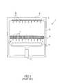
- FIG. 1schematically illustrates an embodiment of a single-wafer processing station 1 that includes a container 2 for receiving a flow of electroplating solution from a fluid inlet 3 at a lower portion of the container 2 .
- the processing station 1can include an anode 4 , a plate-type diffuser 6 having a plurality of apertures 7 , and a workpiece holder 9 for carrying a workpiece 5 .
- the workpiece holder 9can include a plurality of electrical contacts arranged to circumscribe a first diameter. The contacts of the workpiece holder 9 contact a perimeter portion of the workpiece for providing electrical current to the seed layer on the surface of the workpiece 5 .
- the seed layerWhen the seed layer is biased with a negative potential relative to the anode 4 , it acts as a cathode.
- the electroplating fluidflows around the anode 4 , through the apertures 7 in the diffuser 6 , and against the plating surface of the workpiece 5 .
- the electroplating solutionis typically an acidic electrolyte that conducts electrical current between the anode 4 and the cathodic seed layer on the surface of the workpiece 5 . Therefore, ions in the electroplating solution plate the surface of the workpiece 5 .
- the plating machines used in fabricating microelectronic devicesmust meet many specific performance criteria. For example, many processes must be able to form small contacts in submicron recesses, such as vias that are less than 0.5 micron wide and are desirably on the order of 0.1 micron wide.
- the plated metal layersshould also be of a uniform thickness across the surface of the workpiece 5 .
- One factor that influences the uniformity of the plated layer, and especially the integrity of the plated material in the submicron micro-recesses,is the current density across the surface of the workpiece.
- Another objective of electrochemical deposition processes according to the prior artis to maximize the real estate available for forming integrated circuits on the workpiece.
- Existing contact assembliestypically include a plurality of fingers that project radially inwardly from a ring. Each of the fingers includes a contact point, and the contact points are typically arranged to circumscribe a circle with a slightly small diameter than the workpiece.
- the diameter circumscribed by the contact pointsis typically selected to be as close to the perimeter edge of the workpiece as possible. Therefore, a significant number of tool manufacturers have expended significant resources to develop contact rings that minimize the distance that the contacts extend radially inwardly from the perimeter edge of the workpiece.
- the present inventionis directed toward methods for forming microelectronic workpieces used in electrochemical deposition processes, methods of depositing a conductive layer on a microelectronic workpiece, and articles for electrochemical deposition in semiconductor fabrication.
- One aspect of the inventionis directed toward methods for forming microelectronic workpieces that are well-suited for electrochemical deposition processes.
- An embodiment of such a methodcomprises depositing a first conductive material on a workpiece to form an electrically conductive first layer that conforms to the workpiece.
- This embodimentfurther includes forming a seed region defined by a second layer of a second conductive material on the first layer and forming a contact region defined by an exposed portion of the first layer that is not covered by the second layer.
- the contact regioncan extend around at least a portion of the perimeter of the workpiece.
- Another embodiment of a method for forming a microelectronic workpiece in accordance with the inventionincludes depositing a first conductive material on the workpiece, depositing a second conductive material over the first conductive material, and forming a contact region around a perimeter of the workpiece.
- the first materialis a conductive material that forms an electrically conductive contact layer which conforms to submicron recesses in the workpieces.
- the second materialis a different conductive material that is deposited onto the contact layer to form a seed layer.
- the second conductive materialfor example, can be copper.
- the contact regionis an exposed portion of the contact layer that extends radially inwardly from an edge of the workpiece.
- the contact regioncan be an annular band of the first material around the perimeter of the workpiece that is configured to directly engage the contact points of a workpiece holder used in electrochemical deposition chambers.
- the contact regioncan be formed by patterning a resist layer in an annular band around the perimeter of the workpiece and then depositing the second conductive material on the contact layer.
- the contact regioncan be formed by depositing the second conductive material over the entire surface area of the workpiece and then etching a portion of the second conductive material from the perimeter of the workpiece.
- Another aspect of the inventionis a method of depositing a conductive layer on a microelectronic workpiece.
- a methodincludes depositing a first conductive material on the workpiece to form an electrically conductive contact layer that conforms to submicron recesses in the workpiece and then disposing a second conductive layer on the contact layer to form a seed layer.
- the methodalso includes forming a contact region around a perimeter portion of the workpiece that is defined by an exposed portion of the contract layer extending radially inwardly from an edge of the workpiece.
- the methodcontinues by electroplating additional material onto the seed layer in a plating process that includes engaging an electrical contact directly with the contact region and applying a current directly to the contact region in the presence of an electroplating solution.
- Another aspect of the inventionis an article for electrochemical deposition of a conductive layer on a workpiece in the fabrication of microelectronic circuits.
- such an articleincludes a workpiece having a plurality of submicron micro-components that define integrated circuits, a first layer on the workpiece, and a second layer over the first layer.
- the first layeris composed of a first electrically conductive material, and the first layer covers an area of the workpiece having a first diameter.
- the second layerdefines a seed layer composed of a second conducive material different than the first material.
- the second layercovers an area of the workpiece having a second diameter less than the first diameter such that a portion of the first layer along a perimeter edge of the workpiece is exposed.
- the exposed portion of the first layerdefines a contact region for directly engaging contacts of a workpiece holder.
- Another embodiment of an article for electrochemical deposition of a conductive layer on a workpieceincludes a workpiece having a plurality of submicron micro-components that define integrated circuits, a barrier layer on the workpiece, and a seed layer over the barrier layer.
- the barrier layeris composed of a first electrically conductive material.
- the seed layeris composed of a second conductive material different than the first material, and the seed layer covers only a portion of the barrier layer to leave an exposed portion of the barrier layer along a perimeter edge of the workpiece.
- FIG. 1is a schematic cross-sectional view of an electrochemical deposition chamber in accordance with the prior art.
- FIGS. 2 A- 2 Care schematic cross-sectional views illustrating a method for forming a workpiece in accordance with an embodiment of the invention.
- FIG. 3is a schematic cross-sectional view of a workpiece in accordance with an embodiment of the invention loaded into a workpiece holder for an electrochemical deposition process in accordance with a method of the invention.
- FIG. 4is a schematic cross-sectional view of an electrochemical deposition chamber for electroplating workpieces in accordance with embodiments of the invention.
- FIGS. 5 A- 5 Dare schematic cross-sectional views illustrating a method for fabricating a workpiece in accordance with another embodiment of the invention.
- FIGS. 6 A- 6 Care schematic cross-sectional views of a method for fabricating a workpiece in accordance with yet another embodiment of the invention.
- microelectronic workpiecesused in electrochemical deposition processes, methods of depositing conductive layers on microelectronic workpieces, and articles for electrochemical deposition of conductive layers on workpieces in the fabrication of microelectronic circuits.
- micro-device workpieceand “microelectronic workpiece” include semiconductor wafers, field emission displays, read/write heads, micro-mechanical devices, and other types of devices that have very small components.
- aspects of the inventioncan include embodiments that do not have all of the features disclosed in FIGS. 2 - 6 C, or other embodiments can include features in addition to those disclosed in these figures.
- the embodiments disclosed in FIGS. 2 - 6 Care directed toward forming damascene conductive lines, but it will be appreciated that they can also be used to form dual-damascene conductive lines, interlayer contacts, and other components in micro-device workpieces. It will be appreciated that several aspects of the invention are particularly suitable for fabricating submicron components on the order of 0.1-0.75 micron or even less than 0.1 micron, but many aspects of the invention may also be useful to fabricate components larger than one micron.
- FIG. 2Ais a schematic cross-sectional view of a workpiece 100 at one stage of a method in accordance with an embodiment of the invention.
- the workpiece 100includes a substrate 102 and a dielectric layer 104 over the substrate 102 .
- the substrate 102can be a semiconductor substrate that includes a plurality of cells with transistors, shallow trench isolation structures, and other components.
- the substrate 102can alternatively be a glass substrate or other material for other types of micro-devices.
- the dielectric layer 104is typically a silicon dioxide, a borophosphate silicon glass, a tetraethylorthosilicate, or other suitable dielectric material. In the particular embodiment shown in FIG.
- the dielectric layer 104includes a plurality of micro-recesses 106 that can be contact holes, trenches, or other structures.
- the micro-recesses 106typically have a sub-micron width on the order of 0.1-0.5 microns and a depth that can be significantly greater than the width.
- the aspect ratio of the micro-recesses 106can range from 3-8.
- the workpiece 100also includes a first layer 110 of a first conductive material.
- the first layer 110can be a barrier layer composed of tantalum, tungsten, a titanium-tungsten alloy, or other suitable materials that provide good adhesion to the dielectric layer 104 and inhibit migration of bulk fill material to the dielectric layer 104 and/or the substrate 102 .
- the barrier layeris typically deposited to a thickness of 100-5000 ⁇ using chemical vapor deposition, physical vapor deposition, or atomic layer deposition processes.
- FIG. 2Bis a schematic cross-sectional view illustrating a subsequent stage of forming a microelectronic workpiece.
- a second layer 120 of a second conductive materialis deposited over the first layer 110 using chemical vapor deposition, physical vapor deposition, atomic layer deposition and/or electroless plating processes.
- the second layer 120typically defines a seed layer for electroplating additional material onto the workpiece 100 in a manner that fills the micro-recesses 106 with the plated material.
- the second layer 120is typically a copper seed layer. It will be appreciated that other materials can be used for the second layer 120 to plate other types of metals or polymeric materials onto the workpiece 100 .
- the second layer 120can be deposited to a thickness of approximately 100-1000 ⁇ , and generally more preferably to a thickness of 200-500 ⁇ .
- the second layer 120is a copper seed layer having a thickness of approximately 100-300 ⁇ , it is generally discontinuous and has several voids (not shown in FIG. 2B).
- the discontinuity of thin copper seed layersis subject to creating large voids in the plated layer within the micro-recesses.
- copper seed layersare subject to oxidation, which reduces the conductivity of the seed layers.
- the combination of thin copper seed layers and oxidationcauses a drop in the current density from the edge to the center of the workpiece 100 when an electrical contact is engaged directly with the second layer 120 at the perimeter of the workpiece 100 .
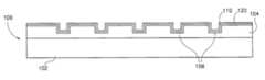
- FIG. 2Cis a schematic cross-sectional view of the workpiece 110 at a subsequent stage of the method.
- This stage of the methodinvolves forming a contact region 130 around a perimeter of the workpiece and a seed region 140 within the contact region 130 .
- the contact region 130 in this embodimentis defined by an exposed portion 132 of the first layer 110 that extends radially inwardly from an edge 134 of the workpiece 100 to the perimeter of the second layer 120 .
- the exposed portion 132 of the first layer 110is not covered by the second material of the second layer 120 .
- the contact region 130can be an annular band extending around the perimeter edge of the workpiece 100 .
- the contact region 130can have a radial width of approximately 1-10 millimeters, and more preferably a radial width of approximately 2-5 millimeters.
- the seed region 140is thus defined by the second layer 120 .
- the first layer 110covers the surface of the workpiece 100 across an area having a first diameter
- the second layer 120covers an area of the first layer 110 having a second diameter less than the first diameter such that a portion of the first layer 110 is exposed along the perimeter edge 134 of the workpiece 100 .
- the embodiment of the workpiece 100 shown in FIG. 2Cis suitable for subsequent electrochemical deposition processing in which a plurality of electrical contacts touch the exposed portion 132 of the first layer 110 to apply an electrical current directly to the first layer 110 without first applying the electrical current to the second layer 120 .
- the contact region 130 shown in FIG. 2Ccan be formed by depositing a layer of resist over the initial deposition of the second layer 120 shown in FIG. 2B (resist not shown). The layer of resist is then patterned and removed around the perimeter of the workpiece, and then the perimeter potion of the second layer 120 is etched away to expose the portion 132 of the first layer 110 shown in FIG. 2C. Suitable photo-patterning and etching processes are well known to those skilled in the art and not described here.
- FIG. 3is a schematic cross-sectional view of the workpiece 100 in a workpiece holder 200 used for electroplating additional material onto the second layer 120 .
- the workpiece holder 200includes a housing 210 , a movable backing plate 220 in one portion of the housing, and an annular rim 230 spaced apart from the backing plate 220 .
- the workpiece holder 200also includes a plurality of contacts 240 arranged in a circle within the rim 230 .
- Each contact 240includes a contact point 242 that is configured to engage the workpiece 100 .
- the contact points 242are generally arranged to circumscribe a circle having a diameter that extends radially inwardly relative to the edge 134 of the workpiece 100 .
- the workpiece 100is loaded into the workpiece holder 200 , and then the backing plate 220 and/or the annular rim 230 moves to press the contact points 242 directly against the exposed portion 132 of the first layer 110 .
- the lip of the rim 230also preferably engages the workpiece 100 to form a seal radially inward from the contact points 242 . It will be appreciated, however, that certain embodiments can be wet-contact plating processes that do not engage a rim with the workpiece.
- the contact points 242accordingly directly engage the surface of the first layer 110 in the contact region to apply an electrical current directly to the first layer. Because the first layer 110 is conductive, the electrical current initially passes through the first layer 110 to provide a uniform current distribution across the workpiece 100 .
- the conductive second layer 120accordingly conducts the electrical current distributed through the first layer 110 to provide a uniform current distribution across the second layer 120 .
- FIG. 4is a schematic cross-sectional view showing an electroplating process for bulk plating material onto the workpiece 100 using the workpiece holder 200 shown in FIG. 3.
- the workpiece holder 200positions the workpiece 100 in a bath of an electroplating solution.
- the workpiece 100is plated in an electrochemical deposition chamber 400 that includes an upper unit 410 having a head 412 that carries the workpiece holder 200 .
- the ECD chamber 400also includes a lower unit 420 that has a bowl 422 for containing an electrolyte bath and an electrode 424 positioned in the bowl 422 .
- the head 412can include a rotor 414 that rotatably carries the workpiece holder 200 .
- the head 412positions the workpiece 100 so that the flow of electrolytic solution engages the face of the workpiece 100 . Additionally, an electrical field is established in the electrolytic solution by applying a potential to the electrode 424 in the bowl 422 and the electrodes 240 contacting the contact region of the workpiece 100 . The ions in the electrolytic bath accordingly attach to the second layer 120 (FIG. 2C) of the workpiece 100 to fill the micro-recesses 106 (FIG. 2C) with the plated material.
- the structure of the workpiece 100 shown in the embodiment of FIG. 2Cis expected to provide a more uniform current distribution in the second layer 120 to produce more uniform plating in the micro-recesses 106 .
- the conductive first layer 110can be a continuous layer without voids even when it is very thin.
- the first layer 110is a thin tantalum layer, it is not subject to including the voids and discontinuities of a thin copper layer.
- thin tantalum layersare not subject to oxidation to the same extent as copper. Therefore, when the contacts 240 apply the current directly to the first layer 110 instead of the second layer 120 , the electrical current is generally uniform through the tantalum layer 110 . This accordingly produces a uniform current distribution through the second layer 120 .
- the embodiments of the workpiece 100 shown in FIG. 2Care expected to produce uniform plating across the face of the workpiece 100 .
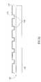
- FIGS. 5 A- 5 Dare schematic cross-sectional views of another embodiment of the workpiece 100 .
- the workpiece 100includes the substrate 102 , the dielectric layer with micro-recesses 106 , and the first layer 110 as described above.
- FIG. 5Bshows the workpiece 100 at a subsequent stage after a layer of resist has been deposited over the workpiece 100 and patterned to form at least one spacer 115 at the perimeter of the workpiece 100 .
- the spacer 115can be a continuous annular ring around the perimeter of the workpiece 100 over the first layer 110 .
- a plurality of discrete spacerscan be formed over areas where the first layer is to be exposed.
- FIG. 5Cillustrates the workpiece 100 at a subsequent stage of the method after having deposited the second layer 120 over the spacer 115 and the first layer 110 .
- the workpiece 100is then subject to a process in which the spacer 115 is removed by a suitable wash or etchant to undercut the perimeter portion of the second layer 120 .
- FIG. 5Dillustrates the workpiece 100 after removing the spacer 115 , which may also remove the undercut portion of the second layer 120 to expose the surface 132 of the first layer 110 and thus define the contact region 130 .
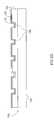
- FIGS. 6 A- 6 Care schematic views illustrating a workpiece 100 a in accordance with yet another embodiment of the invention.
- the workpiece 100 ahas a substrate 102 , a dielectric layer 104 with micro-recesses 106 , and a first layer 110 as explained above.
- the workpiece 100 aalso has a layer of resist 115 a which has been patterned to form large openings over the micro-recesses 106 .
- FIG. 6Billustrates the workpiece 100 a after a second layer 120 has been deposited over the first layer 110 and the resist layer 115 a .
- FIG. 6Cillustrates the workpiece 100 a after removing the top portions of the second layer 120 and the resist layer 115 a .
- the structure shown in FIG. 6Bcan be planarized to remove the top portions of the second layer 120 over the resist layer 115 a , and then the resist 115 a can be removed from the workpiece using a suitable wash or etchant that does not react with the second layer 120 or the first layer 110 .
- the workpiece 100 a shown in FIG. 6Ccan accordingly be loaded into a workpiece holder and electroplated as explained above.
Landscapes
- Engineering & Computer Science (AREA)
- Microelectronics & Electronic Packaging (AREA)
- Computer Hardware Design (AREA)
- Power Engineering (AREA)
- Physics & Mathematics (AREA)
- Condensed Matter Physics & Semiconductors (AREA)
- General Physics & Mathematics (AREA)
- Manufacturing & Machinery (AREA)
- Chemical & Material Sciences (AREA)
- Chemical Kinetics & Catalysis (AREA)
- Organic Chemistry (AREA)
- Metallurgy (AREA)
- Materials Engineering (AREA)
- Electrochemistry (AREA)
- Electroplating Methods And Accessories (AREA)
- Internal Circuitry In Semiconductor Integrated Circuit Devices (AREA)
- Electrodes Of Semiconductors (AREA)
Abstract
Description
- The present invention relates to microelectronic workpieces with barrier layers and seed layers that are configured for electrochemical deposition processing, and methods of making and using such microelectronic workpieces.[0001]
- Microelectronic devices, such as semiconductor devices, field emission displays, read/write heads, and other products that include integrated circuits, are generally fabricated on and/or in microelectronic workpieces using several different types of machines (“tools”). Many such processing machines have a single processing station that performs one or more procedures on the workpieces. In a typical fabrication process, for example, one or more layers of conductive materials are formed on the workpieces during deposition stages. The workpieces are then typically etched and/or planarized (i.e., chemical-mechanical planarization) to remove an “overburden” portion of the deposited conductive layers and thus form electrically isolated contacts and/or interconnect lines.[0002]
- Plating tools that plate metals or other materials onto the workpieces are becoming an increasingly useful type of processing tool. Electroplating and electroless plating techniques can be used to deposit copper, solder, permalloy, gold, silver, platinum, polymeric materials and other materials onto workpieces for forming blanket layers or patterned layers. A typical copper plating process involves depositing a barrier layer on the workpiece that conforms to micro-recesses and other features and then depositing a copper seed layer onto the barrier layer using chemical vapor deposition (CVD), physical vapor deposition (PVD), electroless plating, or other suitable deposition processes. After forming the seed layer, a blanket layer or patterned layer of copper is plated onto the workpiece by applying an appropriate electrical potential between the seed layer and another electrode in the presence of an electroprocessing solution (i.e., an acidic electrolyte). The workpiece is then cleaned, etched, and/or annealed in subsequent procedures before transferring the workpiece to other processing machines.[0003]
- FIG. 1 schematically illustrates an embodiment of a single-[0004]
wafer processing station 1 that includes acontainer 2 for receiving a flow of electroplating solution from afluid inlet 3 at a lower portion of thecontainer 2. Theprocessing station 1 can include ananode 4, a plate-type diffuser 6 having a plurality ofapertures 7, and a workpiece holder9 for carrying aworkpiece 5. The workpiece holder9 can include a plurality of electrical contacts arranged to circumscribe a first diameter. The contacts of the workpiece holder9 contact a perimeter portion of the workpiece for providing electrical current to the seed layer on the surface of theworkpiece 5. When the seed layer is biased with a negative potential relative to theanode 4, it acts as a cathode. In operation, the electroplating fluid flows around theanode 4, through theapertures 7 in thediffuser 6, and against the plating surface of theworkpiece 5. The electroplating solution is typically an acidic electrolyte that conducts electrical current between theanode 4 and the cathodic seed layer on the surface of theworkpiece 5. Therefore, ions in the electroplating solution plate the surface of theworkpiece 5. - The plating machines used in fabricating microelectronic devices must meet many specific performance criteria. For example, many processes must be able to form small contacts in submicron recesses, such as vias that are less than 0.5 micron wide and are desirably on the order of 0.1 micron wide. The plated metal layers should also be of a uniform thickness across the surface of the[0005]
workpiece 5. One factor that influences the uniformity of the plated layer, and especially the integrity of the plated material in the submicron micro-recesses, is the current density across the surface of the workpiece. - Another objective of electrochemical deposition processes according to the prior art is to maximize the real estate available for forming integrated circuits on the workpiece. Existing contact assemblies typically include a plurality of fingers that project radially inwardly from a ring. Each of the fingers includes a contact point, and the contact points are typically arranged to circumscribe a circle with a slightly small diameter than the workpiece. To maximize the available real estate for forming integrated circuits, the diameter circumscribed by the contact points is typically selected to be as close to the perimeter edge of the workpiece as possible. Therefore, a significant number of tool manufacturers have expended significant resources to develop contact rings that minimize the distance that the contacts extend radially inwardly from the perimeter edge of the workpiece.[0006]
- Although electrochemical deposition processes are widely used in semiconductor fabrication applications, it is becoming difficult to form uniform layers that completely fill the submicron micro-recesses. One factor contributing to the difficulty of electrochemical deposition processes is that very thin seed layers are necessary to fill 0.1-0.5 micron recesses. The ultrathin seed layers are typically discontinuous layers of copper that do not uniformly cover the topography of the workpieces. As a result, an IR drop occurs across thin seed layers, and the amount of copper that each contact engages varies across the workpiece. The IR drop is exacerbated because oxidation greatly impairs the conductivity of the copper seed layer. Moreover, acidic electroplating baths momentarily etch the copper seed layer before an electrical current is established in the bath causing a further reduction of conductivity. Thus, reduced conductivity of the copper seed layer further increases the IR drop.[0007]
- The IR drop across the seed layer and the non-uniformities of ultrathin seed layers having a thickness of between 100-1000 Å cause a non-uniform current distribution in which the electrical current at the center of the workpiece is less than the current at the perimeter for an initial portion of the plating cycle. This produces non-uniform surfaces across the workpiece and voids within the submicron micro-recesses. Therefore, the semiconductor industry is currently seeking to reduce such non-uniformities and voids associated with electrochemical deposition processes.[0008]
- The present invention is directed toward methods for forming microelectronic workpieces used in electrochemical deposition processes, methods of depositing a conductive layer on a microelectronic workpiece, and articles for electrochemical deposition in semiconductor fabrication. One aspect of the invention is directed toward methods for forming microelectronic workpieces that are well-suited for electrochemical deposition processes. An embodiment of such a method comprises depositing a first conductive material on a workpiece to form an electrically conductive first layer that conforms to the workpiece. This embodiment further includes forming a seed region defined by a second layer of a second conductive material on the first layer and forming a contact region defined by an exposed portion of the first layer that is not covered by the second layer. The contact region can extend around at least a portion of the perimeter of the workpiece.[0009]
- Another embodiment of a method for forming a microelectronic workpiece in accordance with the invention includes depositing a first conductive material on the workpiece, depositing a second conductive material over the first conductive material, and forming a contact region around a perimeter of the workpiece. The first material is a conductive material that forms an electrically conductive contact layer which conforms to submicron recesses in the workpieces. The second material is a different conductive material that is deposited onto the contact layer to form a seed layer. The second conductive material, for example, can be copper. The contact region is an exposed portion of the contact layer that extends radially inwardly from an edge of the workpiece. The contact region, for example, can be an annular band of the first material around the perimeter of the workpiece that is configured to directly engage the contact points of a workpiece holder used in electrochemical deposition chambers. The contact region can be formed by patterning a resist layer in an annular band around the perimeter of the workpiece and then depositing the second conductive material on the contact layer. Alternatively, the contact region can be formed by depositing the second conductive material over the entire surface area of the workpiece and then etching a portion of the second conductive material from the perimeter of the workpiece.[0010]
- Another aspect of the invention is a method of depositing a conductive layer on a microelectronic workpiece. In one embodiment, such a method includes depositing a first conductive material on the workpiece to form an electrically conductive contact layer that conforms to submicron recesses in the workpiece and then disposing a second conductive layer on the contact layer to form a seed layer. The method also includes forming a contact region around a perimeter portion of the workpiece that is defined by an exposed portion of the contract layer extending radially inwardly from an edge of the workpiece. The method continues by electroplating additional material onto the seed layer in a plating process that includes engaging an electrical contact directly with the contact region and applying a current directly to the contact region in the presence of an electroplating solution.[0011]
- Another aspect of the invention is an article for electrochemical deposition of a conductive layer on a workpiece in the fabrication of microelectronic circuits. In one embodiment, such an article includes a workpiece having a plurality of submicron micro-components that define integrated circuits, a first layer on the workpiece, and a second layer over the first layer. The first layer is composed of a first electrically conductive material, and the first layer covers an area of the workpiece having a first diameter. The second layer defines a seed layer composed of a second conducive material different than the first material. The second layer covers an area of the workpiece having a second diameter less than the first diameter such that a portion of the first layer along a perimeter edge of the workpiece is exposed. The exposed portion of the first layer defines a contact region for directly engaging contacts of a workpiece holder.[0012]
- Another embodiment of an article for electrochemical deposition of a conductive layer on a workpiece includes a workpiece having a plurality of submicron micro-components that define integrated circuits, a barrier layer on the workpiece, and a seed layer over the barrier layer. The barrier layer is composed of a first electrically conductive material. The seed layer is composed of a second conductive material different than the first material, and the seed layer covers only a portion of the barrier layer to leave an exposed portion of the barrier layer along a perimeter edge of the workpiece.[0013]
- FIG. 1 is a schematic cross-sectional view of an electrochemical deposition chamber in accordance with the prior art.[0014]
- FIGS.[0015]2A-2C are schematic cross-sectional views illustrating a method for forming a workpiece in accordance with an embodiment of the invention.
- FIG. 3 is a schematic cross-sectional view of a workpiece in accordance with an embodiment of the invention loaded into a workpiece holder for an electrochemical deposition process in accordance with a method of the invention.[0016]
- FIG. 4 is a schematic cross-sectional view of an electrochemical deposition chamber for electroplating workpieces in accordance with embodiments of the invention.[0017]
- FIGS.[0018]5A-5D are schematic cross-sectional views illustrating a method for fabricating a workpiece in accordance with another embodiment of the invention.
- FIGS.[0019]6A-6C are schematic cross-sectional views of a method for fabricating a workpiece in accordance with yet another embodiment of the invention.
- The following disclosure describes methods for forming microelectronic workpieces used in electrochemical deposition processes, methods of depositing conductive layers on microelectronic workpieces, and articles for electrochemical deposition of conductive layers on workpieces in the fabrication of microelectronic circuits. As used herein, the terms “micro-device workpiece” and “microelectronic workpiece” include semiconductor wafers, field emission displays, read/write heads, micro-mechanical devices, and other types of devices that have very small components. Several embodiments of the invention are described below with reference to FIGS.[0020]2-6C, but it will be appreciated that the invention can include other embodiments not shown in these figures. For example, aspects of the invention can include embodiments that do not have all of the features disclosed in FIGS.2-6C, or other embodiments can include features in addition to those disclosed in these figures. Additionally, the embodiments disclosed in FIGS.2-6C are directed toward forming damascene conductive lines, but it will be appreciated that they can also be used to form dual-damascene conductive lines, interlayer contacts, and other components in micro-device workpieces. It will be appreciated that several aspects of the invention are particularly suitable for fabricating submicron components on the order of 0.1-0.75 micron or even less than 0.1 micron, but many aspects of the invention may also be useful to fabricate components larger than one micron.
- FIG. 2A is a schematic cross-sectional view of a[0021]
workpiece 100 at one stage of a method in accordance with an embodiment of the invention. Theworkpiece 100 includes asubstrate 102 and adielectric layer 104 over thesubstrate 102. Thesubstrate 102 can be a semiconductor substrate that includes a plurality of cells with transistors, shallow trench isolation structures, and other components. Thesubstrate 102 can alternatively be a glass substrate or other material for other types of micro-devices. Thedielectric layer 104 is typically a silicon dioxide, a borophosphate silicon glass, a tetraethylorthosilicate, or other suitable dielectric material. In the particular embodiment shown in FIG. 2A, thedielectric layer 104 includes a plurality ofmicro-recesses 106 that can be contact holes, trenches, or other structures. The micro-recesses106 typically have a sub-micron width on the order of 0.1-0.5 microns and a depth that can be significantly greater than the width. For example, the aspect ratio of the micro-recesses106 can range from 3-8. Theworkpiece 100 also includes afirst layer 110 of a first conductive material. Thefirst layer 110 can be a barrier layer composed of tantalum, tungsten, a titanium-tungsten alloy, or other suitable materials that provide good adhesion to thedielectric layer 104 and inhibit migration of bulk fill material to thedielectric layer 104 and/or thesubstrate 102. The barrier layer is typically deposited to a thickness of 100-5000 Å using chemical vapor deposition, physical vapor deposition, or atomic layer deposition processes. - FIG. 2B is a schematic cross-sectional view illustrating a subsequent stage of forming a microelectronic workpiece. A[0022]
second layer 120 of a second conductive material is deposited over thefirst layer 110 using chemical vapor deposition, physical vapor deposition, atomic layer deposition and/or electroless plating processes. Thesecond layer 120 typically defines a seed layer for electroplating additional material onto theworkpiece 100 in a manner that fills the micro-recesses106 with the plated material. For example, to fill themicro-recesses 106 with copper, thesecond layer 120 is typically a copper seed layer. It will be appreciated that other materials can be used for thesecond layer 120 to plate other types of metals or polymeric materials onto theworkpiece 100. Thesecond layer 120 can be deposited to a thickness of approximately 100-1000 Å, and generally more preferably to a thickness of 200-500 Å. When thesecond layer 120 is a copper seed layer having a thickness of approximately 100-300 Å, it is generally discontinuous and has several voids (not shown in FIG. 2B). The discontinuity of thin copper seed layers is subject to creating large voids in the plated layer within the micro-recesses. Additionally, copper seed layers are subject to oxidation, which reduces the conductivity of the seed layers. The combination of thin copper seed layers and oxidation causes a drop in the current density from the edge to the center of theworkpiece 100 when an electrical contact is engaged directly with thesecond layer 120 at the perimeter of theworkpiece 100. - FIG. 2C is a schematic cross-sectional view of the[0023]
workpiece 110 at a subsequent stage of the method. This stage of the method involves forming acontact region 130 around a perimeter of the workpiece and aseed region 140 within thecontact region 130. Thecontact region 130 in this embodiment is defined by an exposedportion 132 of thefirst layer 110 that extends radially inwardly from anedge 134 of theworkpiece 100 to the perimeter of thesecond layer 120. The exposedportion 132 of thefirst layer 110 is not covered by the second material of thesecond layer 120. Thecontact region 130 can be an annular band extending around the perimeter edge of theworkpiece 100. Thecontact region 130 can have a radial width of approximately 1-10 millimeters, and more preferably a radial width of approximately 2-5 millimeters. Theseed region 140 is thus defined by thesecond layer 120. As a result, thefirst layer 110 covers the surface of theworkpiece 100 across an area having a first diameter, and thesecond layer 120 covers an area of thefirst layer 110 having a second diameter less than the first diameter such that a portion of thefirst layer 110 is exposed along theperimeter edge 134 of theworkpiece 100. The embodiment of theworkpiece 100 shown in FIG. 2C is suitable for subsequent electrochemical deposition processing in which a plurality of electrical contacts touch the exposedportion 132 of thefirst layer 110 to apply an electrical current directly to thefirst layer 110 without first applying the electrical current to thesecond layer 120. - The[0024]
contact region 130 shown in FIG. 2C can be formed by depositing a layer of resist over the initial deposition of thesecond layer 120 shown in FIG. 2B (resist not shown). The layer of resist is then patterned and removed around the perimeter of the workpiece, and then the perimeter potion of thesecond layer 120 is etched away to expose theportion 132 of thefirst layer 110 shown in FIG. 2C. Suitable photo-patterning and etching processes are well known to those skilled in the art and not described here. - FIG. 3 is a schematic cross-sectional view of the[0025]
workpiece 100 in aworkpiece holder 200 used for electroplating additional material onto thesecond layer 120. Theworkpiece holder 200 includes ahousing 210, amovable backing plate 220 in one portion of the housing, and anannular rim 230 spaced apart from thebacking plate 220. Theworkpiece holder 200 also includes a plurality ofcontacts 240 arranged in a circle within therim 230. Eachcontact 240 includes acontact point 242 that is configured to engage theworkpiece 100. The contact points242 are generally arranged to circumscribe a circle having a diameter that extends radially inwardly relative to theedge 134 of theworkpiece 100. - The[0026]
workpiece 100 is loaded into theworkpiece holder 200, and then thebacking plate 220 and/or theannular rim 230 moves to press the contact points242 directly against the exposedportion 132 of thefirst layer 110. The lip of therim 230 also preferably engages theworkpiece 100 to form a seal radially inward from the contact points242. It will be appreciated, however, that certain embodiments can be wet-contact plating processes that do not engage a rim with the workpiece. The contact points242 accordingly directly engage the surface of thefirst layer 110 in the contact region to apply an electrical current directly to the first layer. Because thefirst layer 110 is conductive, the electrical current initially passes through thefirst layer 110 to provide a uniform current distribution across theworkpiece 100. The conductivesecond layer 120 accordingly conducts the electrical current distributed through thefirst layer 110 to provide a uniform current distribution across thesecond layer 120. - FIG. 4 is a schematic cross-sectional view showing an electroplating process for bulk plating material onto the[0027]
workpiece 100 using theworkpiece holder 200 shown in FIG. 3. In operation, theworkpiece holder 200 positions theworkpiece 100 in a bath of an electroplating solution. As shown in FIG. 4, theworkpiece 100 is plated in anelectrochemical deposition chamber 400 that includes anupper unit 410 having ahead 412 that carries theworkpiece holder 200. TheECD chamber 400 also includes alower unit 420 that has abowl 422 for containing an electrolyte bath and anelectrode 424 positioned in thebowl 422. More specifically, thehead 412 can include arotor 414 that rotatably carries theworkpiece holder 200. Thehead 412 positions theworkpiece 100 so that the flow of electrolytic solution engages the face of theworkpiece 100. Additionally, an electrical field is established in the electrolytic solution by applying a potential to theelectrode 424 in thebowl 422 and theelectrodes 240 contacting the contact region of theworkpiece 100. The ions in the electrolytic bath accordingly attach to the second layer120 (FIG. 2C) of theworkpiece 100 to fill the micro-recesses106 (FIG. 2C) with the plated material. - The structure of the[0028]
workpiece 100 shown in the embodiment of FIG. 2C is expected to provide a more uniform current distribution in thesecond layer 120 to produce more uniform plating in the micro-recesses106. The conductivefirst layer 110 can be a continuous layer without voids even when it is very thin. For example, when thefirst layer 110 is a thin tantalum layer, it is not subject to including the voids and discontinuities of a thin copper layer. Additionally, thin tantalum layers are not subject to oxidation to the same extent as copper. Therefore, when thecontacts 240 apply the current directly to thefirst layer 110 instead of thesecond layer 120, the electrical current is generally uniform through thetantalum layer 110. This accordingly produces a uniform current distribution through thesecond layer 120. As a result, by exposing the contact region on thefirst layer 110 and engaging thecontact point 242 of thecontacts 240 directly with the contact region, the embodiments of theworkpiece 100 shown in FIG. 2C are expected to produce uniform plating across the face of theworkpiece 100. - FIGS.[0029]5A-5D are schematic cross-sectional views of another embodiment of the
workpiece 100. Referring to FIG. 5A, theworkpiece 100 includes thesubstrate 102, the dielectric layer withmicro-recesses 106, and thefirst layer 110 as described above. FIG. 5B shows theworkpiece 100 at a subsequent stage after a layer of resist has been deposited over theworkpiece 100 and patterned to form at least onespacer 115 at the perimeter of theworkpiece 100. Thespacer 115 can be a continuous annular ring around the perimeter of theworkpiece 100 over thefirst layer 110. Alternatively, a plurality of discrete spacers can be formed over areas where the first layer is to be exposed. FIG. 5C illustrates theworkpiece 100 at a subsequent stage of the method after having deposited thesecond layer 120 over thespacer 115 and thefirst layer 110. Theworkpiece 100 is then subject to a process in which thespacer 115 is removed by a suitable wash or etchant to undercut the perimeter portion of thesecond layer 120. FIG. 5D illustrates theworkpiece 100 after removing thespacer 115, which may also remove the undercut portion of thesecond layer 120 to expose thesurface 132 of thefirst layer 110 and thus define thecontact region 130. - FIGS.[0030]6A-6C are schematic views illustrating a
workpiece 100ain accordance with yet another embodiment of the invention. Referring to FIG. 6A, theworkpiece 100ahas asubstrate 102, adielectric layer 104 withmicro-recesses 106, and afirst layer 110 as explained above. Theworkpiece 100aalso has a layer of resist115awhich has been patterned to form large openings over the micro-recesses106. FIG. 6B illustrates theworkpiece 100aafter asecond layer 120 has been deposited over thefirst layer 110 and the resistlayer 115a. FIG. 6C illustrates theworkpiece 100aafter removing the top portions of thesecond layer 120 and the resistlayer 115a. To form the structure shown in FIG. 6C from the structure shown in FIG. 6B, the structure shown in FIG. 6B can be planarized to remove the top portions of thesecond layer 120 over the resistlayer 115a, and then the resist115acan be removed from the workpiece using a suitable wash or etchant that does not react with thesecond layer 120 or thefirst layer 110. Theworkpiece 100ashown in FIG. 6C can accordingly be loaded into a workpiece holder and electroplated as explained above. - From the foregoing, it will be appreciated that specific embodiments of the invention have been described herein for purposes of illustration, but that various modifications may be made without deviating from the spirit and scope of the invention. Accordingly, the invention is not limited except as by the appended claims.[0031]
Claims (60)
1. A method of forming a microelectronic workpiece for electrochemical deposition processing, comprising:
depositing a first conductive material on the workpiece to form an electrically conductive contact layer that conforms to submicron recesses in the workpiece;
disposing a second conductive material on at least a portion of the contact layer to form a conformal seed layer; and
forming a contact region around a perimeter of the workpiece, the contact region being an exposed portion of the contact layer extending radially inwardly from an edge of the workpiece.
2. The method ofclaim 1 wherein forming the contact region comprises removing the second conductive material from a perimeter region around the workpiece to expose the first conductive material in a perimeter band.
3. The method ofclaim 1 wherein forming the contact region comprises removing the second conductive material from a perimeter region around the workpiece to expose the first conductive material in a perimeter band having a width of approximately 1-10 mm.
4. The method ofclaim 1 wherein forming the contact region comprises removing the second conductive material from a perimeter region around the workpiece to expose the first conductive material in a perimeter band having a width of approximately 2-5 mm.
5. The method ofclaim 1 wherein:
depositing the first conductive material on the workpiece comprises covering a first area having a first diameter with the first conductive material;
disposing the second conductive material on the workpiece comprises applying the second conductive material directly onto the first conductive material over an area having a diameter at least approximate to the first diameter; and
forming the contact region comprises etching a perimeter portion of the second conductive material so that the second conductive material covers a second area having a second diameter less than the first diameter.
6. The method ofclaim 1 wherein:
depositing the first conductive material on the workpiece comprises covering a first area having a first diameter with the first conductive material;
the method further comprises depositing a resist layer on the first conductive material and patterning the resist layer to form a spacer on the first conductive material before disposing the second conductive material on the first conductive material;
disposing the second conductive material on the workpiece comprises applying the second conductive material directly onto the first conductive material over an area having a second diameter less than the first diameter and on the spacer; and
forming the contact region comprises removing the second conductive material from the spacer and removing the spacer.
7. The method ofclaim 1 wherein:
depositing the first conductive material on the workpiece comprises depositing a barrier layer that inhibits migration of copper; and
disposing the second conductive material on at least a portion of the first conductive material comprises disposing a copper seed layer over the barrier layer.
8. The method ofclaim 7 wherein forming the contact region comprises removing the copper seed layer from a perimeter region around the workpiece to expose the first conductive material in a perimeter band having a width of approximately 2-5 mm.
9. The method ofclaim 7 wherein:
depositing the first conductive material on the workpiece comprises covering a first area having a first diameter with the barrier layer;
disposing the second conductive material on the workpiece comprises applying the copper seed layer directly onto the barrier layer over an area having a diameter at least approximate to the first diameter; and
forming the contact region comprises etching a perimeter portion of the seed layer so that the seed layer covers a second area having a second diameter less than the first diameter.
10. The method ofclaim 7 wherein:
depositing the first conductive material on the workpiece comprises covering a first area having a first diameter with the barrier layer;
the method further comprises depositing a resist layer on the barrier layer and patterning the resist layer to form spacers before disposing the copper seed layer on the barrier layer;
disposing the second conductive material on the workpiece comprises applying the seed layer directly on the spacers and on the barrier layer over an area having a second diameter less than the first diameter; and
forming the contact region comprises removing the second conductive material from the spacers and removing the spacers.
11. A method of forming a microelectronic workpiece for electrochemical deposition processing, comprising:
depositing a first conductive material on the workpiece to form an electrically conductive first layer that conforms to the workpiece; and
forming a seed region defined by a second layer of a second conductive material on the first layer and a contact region defined by an exposed portion of the first layer that is not covered by the second layer, wherein the contact region is around at least a perimeter portion of the workpiece.
12. The method ofclaim 11 wherein forming the contact region comprises removing the second conductive material from a perimeter region around the workpiece to expose the first conductive material in a perimeter band.
13. The method ofclaim 11 wherein forming the contact region comprises removing the second conductive material from a perimeter region around the workpiece to expose the first conductive material in a perimeter band having a width of approximately 2-5 mm.
14. The method ofclaim 11 wherein:
depositing the first conductive material on the workpiece comprises covering a first area having a first diameter with the first conductive material;
forming the seed region comprises disposing the second conductive material on the workpiece by applying the second conductive material directly onto the first conductive material over an area having a diameter at least approximate to the first diameter; and
forming the contact region comprises etching a perimeter portion of the second conductive material so that the second conductive material covers a second area having a second diameter less than the first diameter.
15. The method ofclaim 11 wherein:
depositing the first conductive material on the workpiece comprises covering a first area having a first diameter with the first conductive material;
the method further comprises depositing a resist layer on the first conductive material and patterning the resist layer to form spacers on the first conductive material before disposing the second conductive material on the first conductive material;
forming the seed region comprises disposing the second conductive material on the workpiece by applying the second conductive material directly onto the first conductive material over an area having a second diameter less than the first diameter and on the spacers; and
forming the contact region comprises removing the second conductive material from the spacers and removing the spacers.
16. The method ofclaim 11 wherein:
depositing the first conductive material on the workpiece comprises depositing a barrier layer that inhibits migration of copper; and
forming the seed region comprises disposing the second conductive material on at least a portion of the first conductive material by disposing a copper seed layer over the barrier layer.
17. A method of forming a microelectronic workpiece for electrochemical deposition processing in an ECD chamber having a workpiece holder including a plurality of contacts having contact points circumscribing a first diameter, the method comprising:
depositing a first conductive material on the workpiece to form a conformal barrier layer;
disposing a second conductive material on at least a portion of the barrier layer to form a seed layer for a subsequent electrochemical deposition procedure; and
forming a contact region comprising an exposed band of the barrier layer that is not covered by the second conductive material, the exposed band of the barrier layer having a diameter encompassing the first diameter circumscribed by the contact points of the workpiece holder.
18. The method ofclaim 17 wherein forming the contact region comprises removing the second conductive material from a perimeter region around the workpiece to expose the first conductive material in a perimeter band.
19. The method ofclaim 17 wherein forming the contact region comprises removing the second conductive material from a perimeter region around the workpiece to expose the first conductive material in a perimeter band having a width of approximately 1-10 mm.
20. The method ofclaim 17 wherein forming the contact region comprises removing the second conductive material from a perimeter region around the workpiece to expose the first conductive material in a perimeter band having a width of approximately 2-5 mm.
21. The method ofclaim 17 wherein:
depositing the first conductive material on the workpiece comprises depositing a barrier layer that inhibits migration of copper; and
disposing the second conductive material on at least a portion of the first conductive material comprises disposing a copper seed layer over the barrier layer.
22. The method ofclaim 21 wherein forming the contact region comprises removing the copper seed layer from a perimeter region around the workpiece to expose the first conductive material in a perimeter band having a width of approximately 2-5 mm.
23. The method ofclaim 21 wherein:
depositing the first conductive material on the workpiece comprises covering a first area having a first diameter with the barrier layer;
disposing the second conductive material on the workpiece comprises applying the copper seed layer directly onto the barrier layer over an area having a diameter at least approximate to the first diameter; and
forming the contact region comprises etching a perimeter portion of the seed layer so that the seed layer covers a second area having a second diameter less than the first diameter.
24. A method of forming a microelectronic workpiece for electrochemical deposition processing comprising:
depositing a first conductive material to form an electrically conductive barrier layer that conforms to the workpiece;
disposing a second conductive material on at least a portion of the barrier layer to form a seed layer; and
removing a portion of the seed layer around a perimeter portion of the workpiece to expose a portion of the barrier layer, wherein the exposed portion of the barrier layer defines a contact region configured to be directly engaged by an electrical contact.
25. The method ofclaim 24 wherein:
depositing the first conductive material on the workpiece comprises depositing a barrier layer that inhibits migration of copper; and
disposing the second conductive material on at least a portion of the first barrier layer comprises disposing a copper seed layer over the barrier layer.
26. The method ofclaim 25 wherein forming the contact region comprises removing the copper seed layer from a perimeter region around the workpiece to expose the first conductive material in a perimeter band having a width of approximately 2-5 mm.
27. The method ofclaim 25 wherein:
depositing the first conductive material on the workpiece comprises covering a first area having a first diameter with the barrier layer;
disposing the second conductive material on the workpiece comprises applying the copper seed layer directly onto the barrier layer over an area having a diameter at least approximate to the first diameter; and
forming the contact region comprises etching a perimeter portion of the seed layer so that the seed layer covers a second area having a second diameter less than the first diameter.
28. A method of depositing a conductive layer on a microelectronic workpiece, comprising:
depositing a first conductive material on the workpiece to form an electrically conductive contact layer that conforms to submicron recesses in the workpiece;
disposing a second conductive material on the contact layer to form a seed layer;
forming a contact region around a perimeter of the workpiece, the contact region being an exposed portion of the contact layer extending radially inwardly from an edge of the workpiece; and
electroplating additional material onto the seed layer by engaging an electrical contact directly with the contact region and applying a current directly to the contact region in the presence of an electroplating solution.
29. The method ofclaim 28 wherein forming the contact region comprises removing the second conductive material from a perimeter region around the workpiece to expose the first conductive material in a perimeter band.
30. The method ofclaim 28 wherein forming the contact region comprises removing the second conductive material from a perimeter region around the workpiece to expose the first conductive material in a perimeter band having a width of approximately 1-10 mm.
31. The method ofclaim 28 wherein forming the contact region comprises removing the second conductive material from a perimeter region around the workpiece to expose the first conductive material in a perimeter band having a width of approximately 2-5 mm.
32. The method ofclaim 28 wherein:
depositing the first conductive material on the workpiece comprises covering a first area having a first diameter with the first conductive material;
disposing the second conductive material on the workpiece comprises applying the second conductive material directly onto the first conductive material over an area having a diameter at least approximate to the first diameter; and
forming the contact region comprises etching a perimeter portion of the second conductive material so that the second conductive material covers a second area having a second diameter less than the first diameter.
33. The method ofclaim 28 wherein:
depositing the first conductive material on the workpiece comprises covering a first area having a first diameter with the first conductive material;
the method further comprises depositing a resist layer on the first conductive material and patterning the resist layer to form a spacer on the first conductive material before disposing the second conductive material on the first conductive material;
disposing the second conductive material on the workpiece comprises applying the second conductive material directly onto the first conductive material over an area having a second diameter less than the first diameter and on the spacer; and
forming the contact region comprises removing the second conductive material from the spacer and removing the spacer.
34. The method ofclaim 28 wherein:
depositing the first conductive material on the workpiece comprises depositing a barrier layer that inhibits migration of copper; and
disposing the second conductive material on at least a portion of the first conductive material comprises disposing a copper seed layer over the barrier layer.
35. The method ofclaim 34 wherein forming the contact region comprises removing the copper seed layer from a perimeter region around the workpiece to expose the first conductive material in a perimeter band having a width of approximately 2-5 mm.
36. The method ofclaim 34 wherein:
depositing the first conductive material on the workpiece comprises covering a first area having a first diameter with the barrier layer;
disposing the second conductive material on the workpiece comprises applying the copper seed layer directly onto the barrier layer over an area having a diameter at least approximate to the first diameter; and
forming the contact region comprises etching a perimeter portion of the seed layer so that the seed layer covers a second area having a second diameter less than the first diameter.
37. The method ofclaim 34 wherein:
depositing the first conductive material on the workpiece comprises covering a first area having a first diameter with the barrier layer;
the method further comprises depositing a resist layer on the barrier and patterning the resist layer to form a spacer before disposing the copper seed layer on the barrier layer;
disposing the second conductive material on the workpiece comprises applying the seed layer directly on the spacer and on the barrier layer over an area having a second diameter less than the first diameter; and
forming the contact region comprises removing the second conductive material from the spacer and removing the spacer.
38. A method of depositing a conductive layer on a microelectronic workpiece, comprising:
depositing a first conductive material on the workpiece to form an electrically conductive first layer that conforms to the workpiece;
forming a seed region defined by a second layer of a second conductive material on the first layer and a contact region defined by an exposed portion of the first layer that is not covered by the second layer, wherein the contact region is around at least a perimeter portion of the workpiece; and
electroplating additional material onto the seed region by engaging an electrical contact directly with the contact region and applying a current directly to the contact region in the presence of an electroplating solution.
39. The method ofclaim 38 wherein forming the contact region comprises removing the second conductive material from a perimeter region around the workpiece to expose the first conductive material in a perimeter band.
40. The method ofclaim 38 wherein forming the contact region comprises removing the second conductive material from a perimeter region around the workpiece to expose the first conductive material in a perimeter band having a width of approximately 2-5 mm.
41. The method ofclaim 38 wherein:
depositing the first conductive material on the workpiece comprises covering a first area having a first diameter with the first conductive material;
forming the seed region comprises disposing the second conductive material on the workpiece by applying the second conductive material directly onto the first conductive material over an area having a diameter at least approximate to the first diameter; and
forming the contact region comprises etching a perimeter portion of the second conductive material so that the second conductive material covers a second area having a second diameter less than the first diameter.
42. The method ofclaim 38 wherein:
depositing the first conductive material on the workpiece comprises covering a first area having a first diameter with the first conductive material;
the method further comprises depositing a resist layer on the first conductive material and patterning the resist layer to form a spacer on the first conductive material before disposing the second conductive material on the first conductive material;
forming the seed region comprises disposing the second conductive material on the workpiece by applying the second conductive material directly onto the first conductive material over an area having a second diameter less than the first diameter and on the spacer; and
forming the contact region comprises removing the second conductive material from the spacer and removing the spacer.
43. The method ofclaim 38 wherein:
depositing the first conductive material on the workpiece comprises depositing a barrier layer that inhibits migration of copper; and
forming the seed region comprises disposing the second conductive material on at least a portion of the first conductive material by disposing a copper seed layer over the barrier layer.
44. A method of electrochemical deposition processing in an ECD chamber having a workpiece holder including a plurality of contacts having contact points circumscribing a first diameter, the method comprising:
depositing a first conductive material on a workpiece to form a conformal barrier layer;
disposing a second conductive material on at least a portion of the barrier layer to form a seed layer for a subsequent electrochemical deposition procedure;
forming a contact region comprising an exposed band of the barrier layer that is not covered by the second conductive material, the exposed band of the barrier layer having a diameter encompassing the first diameter circumscribed by the contact points of the workpiece holder; and
electroplating additional material onto the seed layer by engaging an electrical contact directly with the exposed band of the barrier layer, contacting the seed layer with an electrochemical solution, and applying a current directly to the exposed band of the carrier layer.
45. A method of depositing a conductive layer on a microelectronic workpiece, comprising:
depositing a first conductive material to form an electrically conductive barrier layer that conforms to submicron recesses in the workpiece;
disposing a second conductive material on the barrier layer to form a seed layer;
removing a portion of the seed layer around a perimeter of the workpiece to expose a portion of the barrier layer, wherein the exposed portion of the barrier layer defines a contact region configured to be directly engaged by an electrical contact; and
electroplating additional material onto the seed layer by engaging an electrical contact directly with the contact region, contacting the seed layer with an electrochemical solution, and applying a current directly to the contact region.
46. An article for electrochemical deposition of a conductive layer on a workpiece in the fabrication of microelectronic circuits, comprising:
a workpiece having a plurality of submicron micro-components that define integrated circuits;
a first layer on the workpiece, the first layer being composed of a first electrically conductive material, and the first layer covering an area of the workpiece having a first diameter;
a second layer over the first layer to define a seed layer, the second layer being composed of a second conductive material different than the first material, and the second layer covering an area of the workpiece having a second diameter less than the first diameter such that a portion of the first layer along a perimeter edge of the workpiece is exposed.
47. The article ofclaim 46 wherein:
the first layer comprises a barrier layer that inhibits migration of copper; and
the second layer comprises copper.
48. The article ofclaim 47 wherein the exposed portion of the first layer comprises a band around the perimeter of the workpiece having a width of approximately 1-10 mm.
49. The article ofclaim 47 wherein the exposed portion of the first layer comprises a band around the perimeter of the workpiece having a width of approximately 2-5 mm.
50. The article ofclaim 46 wherein the exposed portion of the first layer has a width extending radially inwardly from a perimeter of the workpiece for a distance of approximately 1-10 mm along at least a portion of the workpiece.
51. The article ofclaim 50 wherein the exposed portion of the first layer comprises a band extend completely around the workpiece.
52. The article ofclaim 50 wherein the exposed portion of the first layer comprises an arc extending only around a portion of the workpiece.
53. An article for electrochemical deposition of a conductive layer on a workpiece in the fabrication of microelectronic circuits, comprising:
a workpiece having a plurality of submicron micro-components that define integrated circuits;
a barrier layer on the workpiece, the barrier layer being composed of a first electrically conductive material that covers an area of the workpiece having a first diameter;
a seed layer over the barrier layer, the seed layer being composed of a second conductive material different than the first material, and the seed layer covering an area of the workpiece having a second diameter less than the first diameter such that a portion of the barrier is exposed along a perimeter edge of the workpiece.
54. The article ofclaim 53 wherein:
the first layer comprises a barrier layer that inhibits migration of copper; and
the second layer comprises copper.
55. The article ofclaim 54 wherein the exposed portion of the first layer comprises a band around the perimeter of the workpiece having a width of approximately 1-10 mm.
56. The article ofclaim 54 wherein the exposed portion of the first layer comprises a band around the perimeter of the workpiece having a width of approximately 2-5 mm.
57. The article ofclaim 53 wherein the exposed portion of the first layer has a width extending radially inwardly from a perimeter of the workpiece for a distance of approximately 1-10 mm along at least a portion of the workpiece.
58. The article ofclaim 57 wherein the exposed portion of the first layer comprises a band extend completely around the workpiece.
59. The article ofclaim 57 wherein the exposed portion of the first layer comprises an arc extending only around a portion of the workpiece.
60. An article for electrochemical deposition of a conductive layer on a workpiece in the fabrication of microelectronic circuits, comprising:
a workpiece having a plurality of submicron micro-components that define integrated circuits;
a barrier layer on the workpiece, the barrier layer being composed of a first electrically conductive material; and
a seed layer composed of a second conductive material different than the first material, wherein the seed layer covers only a portion of the barrier layer to leave an exposed portion of the barrier layer along a perimeter edge of the workpiece.
Priority Applications (2)
| Application Number | Priority Date | Filing Date | Title |
|---|---|---|---|
| US10/225,585US7025866B2 (en) | 2002-08-21 | 2002-08-21 | Microelectronic workpiece for electrochemical deposition processing and methods of manufacturing and using such microelectronic workpieces |
| US11/348,202US20060182879A1 (en) | 2002-08-21 | 2006-02-06 | Microelectronic workpiece for electrochemical deposition processing and methods of manufacturing and using such microelectronic workpieces |
Applications Claiming Priority (1)
| Application Number | Priority Date | Filing Date | Title |
|---|---|---|---|
| US10/225,585US7025866B2 (en) | 2002-08-21 | 2002-08-21 | Microelectronic workpiece for electrochemical deposition processing and methods of manufacturing and using such microelectronic workpieces |
Related Child Applications (1)
| Application Number | Title | Priority Date | Filing Date |
|---|---|---|---|
| US11/348,202DivisionUS20060182879A1 (en) | 2002-08-21 | 2006-02-06 | Microelectronic workpiece for electrochemical deposition processing and methods of manufacturing and using such microelectronic workpieces |
Publications (2)
| Publication Number | Publication Date |
|---|---|
| US20040038052A1true US20040038052A1 (en) | 2004-02-26 |
| US7025866B2 US7025866B2 (en) | 2006-04-11 |
Family
ID=31887035
Family Applications (2)
| Application Number | Title | Priority Date | Filing Date |
|---|---|---|---|
| US10/225,585Expired - Fee RelatedUS7025866B2 (en) | 2002-08-21 | 2002-08-21 | Microelectronic workpiece for electrochemical deposition processing and methods of manufacturing and using such microelectronic workpieces |
| US11/348,202AbandonedUS20060182879A1 (en) | 2002-08-21 | 2006-02-06 | Microelectronic workpiece for electrochemical deposition processing and methods of manufacturing and using such microelectronic workpieces |
Family Applications After (1)
| Application Number | Title | Priority Date | Filing Date |
|---|---|---|---|
| US11/348,202AbandonedUS20060182879A1 (en) | 2002-08-21 | 2006-02-06 | Microelectronic workpiece for electrochemical deposition processing and methods of manufacturing and using such microelectronic workpieces |
Country Status (1)
| Country | Link |
|---|---|
| US (2) | US7025866B2 (en) |
Cited By (7)
| Publication number | Priority date | Publication date | Assignee | Title |
|---|---|---|---|---|
| US20060046454A1 (en)* | 2004-09-01 | 2006-03-02 | Micron Technology, Inc. | Method for filling electrically different features |
| US20060137994A1 (en)* | 2001-12-21 | 2006-06-29 | Basol Bulent M | Method of wafer processing with edge seed layer removal |
| US20060182879A1 (en)* | 2002-08-21 | 2006-08-17 | Collins Dale W | Microelectronic workpiece for electrochemical deposition processing and methods of manufacturing and using such microelectronic workpieces |
| US20070155145A1 (en)* | 2005-12-29 | 2007-07-05 | Dongbu Electronics Co., Ltd. | Method for forming a copper metal interconnection of a semiconductor device using two seed layers |
| US20080160749A1 (en)* | 2006-12-27 | 2008-07-03 | Texas Instruments Incorporated | Semiconductor device and method of forming thereof |
| US20090078580A1 (en)* | 2005-12-02 | 2009-03-26 | Ulvac, Inc. | Method for Forming Cu Film |
| US20230086742A1 (en)* | 2021-09-23 | 2023-03-23 | Applied Materials, Inc. | Methods for electrochemical deposition of isolated seed layer areas |
Families Citing this family (2)
| Publication number | Priority date | Publication date | Assignee | Title |
|---|---|---|---|---|
| US7144490B2 (en)* | 2003-11-18 | 2006-12-05 | International Business Machines Corporation | Method for selective electroplating of semiconductor device I/O pads using a titanium-tungsten seed layer |
| US20080217183A1 (en)* | 2007-03-09 | 2008-09-11 | Sriram Muthukumar | Electropolishing metal features on a semiconductor wafer |
Citations (71)
| Publication number | Priority date | Publication date | Assignee | Title |
|---|---|---|---|---|
| US2003A (en)* | 1841-03-12 | Improvement in horizontal windivhlls | ||
| US2002A (en)* | 1841-03-12 | Tor and planter for plowing | ||
| US3267010A (en)* | 1962-04-16 | 1966-08-16 | Udylite Corp | Electrodeposition of copper from acidic baths |
| US3328273A (en)* | 1966-08-15 | 1967-06-27 | Udylite Corp | Electro-deposition of copper from acidic baths |
| US3664933A (en)* | 1969-06-19 | 1972-05-23 | Udylite Corp | Process for acid copper plating of zinc |
| US3716462A (en)* | 1970-10-05 | 1973-02-13 | D Jensen | Copper plating on zinc and its alloys |
| US3770598A (en)* | 1972-01-21 | 1973-11-06 | Oxy Metal Finishing Corp | Electrodeposition of copper from acid baths |
| US3878066A (en)* | 1972-09-06 | 1975-04-15 | Manfred Dettke | Bath for galvanic deposition of gold and gold alloys |
| US3930963A (en)* | 1971-07-29 | 1976-01-06 | Photocircuits Division Of Kollmorgen Corporation | Method for the production of radiant energy imaged printed circuit boards |
| US4000046A (en)* | 1974-12-23 | 1976-12-28 | P. R. Mallory & Co., Inc. | Method of electroplating a conductive layer over an electrolytic capacitor |
| US4134802A (en)* | 1977-10-03 | 1979-01-16 | Oxy Metal Industries Corporation | Electrolyte and method for electrodepositing bright metal deposits |
| US4272335A (en)* | 1980-02-19 | 1981-06-09 | Oxy Metal Industries Corporation | Composition and method for electrodeposition of copper |
| US4279948A (en)* | 1978-05-25 | 1981-07-21 | Macdermid Incorporated | Electroless copper deposition solution using a hypophosphite reducing agent |
| US4417956A (en)* | 1980-07-17 | 1983-11-29 | Electrochemical Products, Inc. | Alkaline plating baths and electroplating process |
| US4576689A (en)* | 1979-06-19 | 1986-03-18 | Makkaev Almaxud M | Process for electrochemical metallization of dielectrics |
| US4624749A (en)* | 1985-09-03 | 1986-11-25 | Harris Corporation | Electrodeposition of submicrometer metallic interconnect for integrated circuits |
| US4959278A (en)* | 1988-06-16 | 1990-09-25 | Nippon Mining Co., Ltd. | Tin whisker-free tin or tin alloy plated article and coating technique thereof |
| US4990224A (en)* | 1988-12-21 | 1991-02-05 | International Business Machines Corporation | Copper plating bath and process for difficult to plate metals |
| US5021129A (en)* | 1989-09-25 | 1991-06-04 | International Business Machines Corporation | Multilayer structures of different electroactive materials and methods of fabrication thereof |
| US5115430A (en)* | 1990-09-24 | 1992-05-19 | At&T Bell Laboratories | Fair access of multi-priority traffic to distributed-queue dual-bus networks |
| US5116430A (en)* | 1990-02-09 | 1992-05-26 | Nihon Parkerizing Co., Ltd. | Process for surface treatment titanium-containing metallic material |
| US5151168A (en)* | 1990-09-24 | 1992-09-29 | Micron Technology, Inc. | Process for metallizing integrated circuits with electrolytically-deposited copper |
| US5161168A (en)* | 1991-05-15 | 1992-11-03 | Scs Mobilecom, Inc. | Spread spectrum CDMA communications system microwave overlay |
| US5209817A (en)* | 1991-08-22 | 1993-05-11 | International Business Machines Corporation | Selective plating method for forming integral via and wiring layers |
| US5256274A (en)* | 1990-08-01 | 1993-10-26 | Jaime Poris | Selective metal electrodeposition process |
| US5284548A (en)* | 1993-03-03 | 1994-02-08 | Microelectronics And Computer Technology Corporation | Process for producing electrical circuits with precision surface features |
| US5368711A (en)* | 1990-08-01 | 1994-11-29 | Poris; Jaime | Selective metal electrodeposition process and apparatus |
| US5372848A (en)* | 1992-12-24 | 1994-12-13 | International Business Machines Corporation | Process for creating organic polymeric substrate with copper |
| US5409587A (en)* | 1993-09-16 | 1995-04-25 | Micron Technology, Inc. | Sputtering with collinator cleaning within the sputtering chamber |
| US5443865A (en)* | 1990-12-11 | 1995-08-22 | International Business Machines Corporation | Method for conditioning a substrate for subsequent electroless metal deposition |
| US5472592A (en)* | 1994-07-19 | 1995-12-05 | American Plating Systems | Electrolytic plating apparatus and method |
| US5482891A (en)* | 1995-03-17 | 1996-01-09 | Motorola, Inc. | VCSEL with an intergrated heat sink and method of making |
| US5549808A (en)* | 1995-05-12 | 1996-08-27 | International Business Machines Corporation | Method for forming capped copper electrical interconnects |
| US5576052A (en)* | 1996-04-22 | 1996-11-19 | Motorola, Inc. | Method of metallizing high aspect ratio apertures |
| US5639316A (en)* | 1995-01-13 | 1997-06-17 | International Business Machines Corp. | Thin film multi-layer oxygen diffusion barrier consisting of aluminum on refractory metal |
| US5674787A (en)* | 1996-01-16 | 1997-10-07 | Sematech, Inc. | Selective electroless copper deposited interconnect plugs for ULSI applications |
| US5695810A (en)* | 1996-11-20 | 1997-12-09 | Cornell Research Foundation, Inc. | Use of cobalt tungsten phosphide as a barrier material for copper metallization |
| US5719447A (en)* | 1993-06-03 | 1998-02-17 | Intel Corporation | Metal alloy interconnections for integrated circuits |
| US5723387A (en)* | 1996-07-22 | 1998-03-03 | Industrial Technology Research Institute | Method and apparatus for forming very small scale Cu interconnect metallurgy on semiconductor substrates |
| US5730854A (en)* | 1996-05-30 | 1998-03-24 | Enthone-Omi, Inc. | Alkoxylated dimercaptans as copper additives and de-polarizing additives |
| US5750018A (en)* | 1997-03-18 | 1998-05-12 | Learonal, Inc. | Cyanide-free monovalent copper electroplating solutions |
| US5788778A (en)* | 1996-09-16 | 1998-08-04 | Applied Komatsu Technology, Inc. | Deposition chamber cleaning technique using a high power remote excitation source |
| US5824599A (en)* | 1996-01-16 | 1998-10-20 | Cornell Research Foundation, Inc. | Protected encapsulation of catalytic layer for electroless copper interconnect |
| US5882498A (en)* | 1997-10-16 | 1999-03-16 | Advanced Micro Devices, Inc. | Method for reducing oxidation of electroplating chamber contacts and improving uniform electroplating of a substrate |
| US5891513A (en)* | 1996-01-16 | 1999-04-06 | Cornell Research Foundation | Electroless CU deposition on a barrier layer by CU contact displacement for ULSI applications |
| US5897368A (en)* | 1997-11-10 | 1999-04-27 | General Electric Company | Method of fabricating metallized vias with steep walls |
| US5908543A (en)* | 1997-02-03 | 1999-06-01 | Okuno Chemical Industries Co., Ltd. | Method of electroplating non-conductive materials |
| US5913147A (en)* | 1997-01-21 | 1999-06-15 | Advanced Micro Devices, Inc. | Method for fabricating copper-aluminum metallization |
| US5932286A (en)* | 1993-03-16 | 1999-08-03 | Applied Materials, Inc. | Deposition of silicon nitride thin films |
| US5932077A (en)* | 1998-02-09 | 1999-08-03 | Reynolds Tech Fabricators, Inc. | Plating cell with horizontal product load mechanism |
| US5969422A (en)* | 1997-05-15 | 1999-10-19 | Advanced Micro Devices, Inc. | Plated copper interconnect structure |
| US5972192A (en)* | 1997-07-23 | 1999-10-26 | Advanced Micro Devices, Inc. | Pulse electroplating copper or copper alloys |
| US6036836A (en)* | 1996-12-20 | 2000-03-14 | Peeters; Joris Antonia Franciscus | Process to create metallic stand-offs on an electronic circuit |
| US6065424A (en)* | 1995-12-19 | 2000-05-23 | Cornell Research Foundation, Inc. | Electroless deposition of metal films with spray processor |
| US6069068A (en)* | 1997-05-30 | 2000-05-30 | International Business Machines Corporation | Sub-quarter-micron copper interconnections with improved electromigration resistance and reduced defect sensitivity |
| US6109206A (en)* | 1997-05-29 | 2000-08-29 | Applied Materials, Inc. | Remote plasma source for chamber cleaning |
| US6113771A (en)* | 1998-04-21 | 2000-09-05 | Applied Materials, Inc. | Electro deposition chemistry |
| US6140234A (en)* | 1998-01-20 | 2000-10-31 | International Business Machines Corporation | Method to selectively fill recesses with conductive metal |
| US6197688B1 (en)* | 1998-02-12 | 2001-03-06 | Motorola Inc. | Interconnect structure in a semiconductor device and method of formation |
| US6197181B1 (en)* | 1998-03-20 | 2001-03-06 | Semitool, Inc. | Apparatus and method for electrolytically depositing a metal on a microelectronic workpiece |
| US6210781B1 (en)* | 1994-06-06 | 2001-04-03 | International Business Machines Corporation | Method for photoselective seeding and metallization of three-dimensional materials |
| US6290833B1 (en)* | 1998-03-20 | 2001-09-18 | Semitool, Inc. | Method for electrolytically depositing copper on a semiconductor workpiece |
| US6309524B1 (en)* | 1998-07-10 | 2001-10-30 | Semitool, Inc. | Methods and apparatus for processing the surface of a microelectronic workpiece |
| US6319831B1 (en)* | 1999-03-18 | 2001-11-20 | Taiwan Semiconductor Manufacturing Company | Gap filling by two-step plating |
| US6329297B1 (en)* | 2000-04-21 | 2001-12-11 | Applied Materials, Inc. | Dilute remote plasma clean |
| US6374831B1 (en)* | 1999-02-04 | 2002-04-23 | Applied Materials, Inc. | Accelerated plasma clean |
| US6387207B1 (en)* | 2000-04-28 | 2002-05-14 | Applied Materials, Inc. | Integration of remote plasma generator with semiconductor processing chamber |
| US6413383B1 (en)* | 1999-10-08 | 2002-07-02 | Applied Materials, Inc. | Method for igniting a plasma in a sputter reactor |
| US6413436B1 (en)* | 1999-01-27 | 2002-07-02 | Semitool, Inc. | Selective treatment of the surface of a microelectronic workpiece |
| US6482307B2 (en)* | 2000-05-12 | 2002-11-19 | Nutool, Inc. | Method of and apparatus for making electrical contact to wafer surface for full-face electroplating or electropolishing |
| US6790776B2 (en)* | 1999-08-16 | 2004-09-14 | Applied Materials, Inc. | Barrier layer for electroplating processes |
Family Cites Families (8)
| Publication number | Priority date | Publication date | Assignee | Title |
|---|---|---|---|---|
| JPS5216433A (en) | 1975-07-30 | 1977-02-07 | Furukawa Electric Co Ltd | Method of producing very thin copper foil |
| JPH06349952A (en) | 1993-06-14 | 1994-12-22 | Oki Electric Ind Co Ltd | Wiring forming method |
| JPH07193214A (en) | 1993-12-27 | 1995-07-28 | Mitsubishi Electric Corp | Via hole and method of forming the same |
| US6198688B1 (en)* | 1998-04-02 | 2001-03-06 | Hyundai Electronics Industries, Co., Ltd. | Interface for synchronous semiconductor memories |
| US6198181B1 (en)* | 1999-11-22 | 2001-03-06 | General Electric Company | Motor design methods and motors fabricated therefrom |
| KR100760337B1 (en) | 1999-12-15 | 2007-09-20 | 롬 앤드 하스 일렉트로닉 머트어리얼즈, 엘.엘.씨 | Seed layer repair method |
| WO2002004704A2 (en) | 2000-07-11 | 2002-01-17 | Applied Materials, Inc. | Method and apparatus for patching electrochemically deposited layers using electroless deposited materials |
| US7025866B2 (en)* | 2002-08-21 | 2006-04-11 | Micron Technology, Inc. | Microelectronic workpiece for electrochemical deposition processing and methods of manufacturing and using such microelectronic workpieces |
- 2002
- 2002-08-21USUS10/225,585patent/US7025866B2/ennot_activeExpired - Fee Related
- 2006
- 2006-02-06USUS11/348,202patent/US20060182879A1/ennot_activeAbandoned
Patent Citations (73)
| Publication number | Priority date | Publication date | Assignee | Title |
|---|---|---|---|---|
| US2003A (en)* | 1841-03-12 | Improvement in horizontal windivhlls | ||
| US2002A (en)* | 1841-03-12 | Tor and planter for plowing | ||
| US3267010A (en)* | 1962-04-16 | 1966-08-16 | Udylite Corp | Electrodeposition of copper from acidic baths |
| US3328273A (en)* | 1966-08-15 | 1967-06-27 | Udylite Corp | Electro-deposition of copper from acidic baths |
| US3664933A (en)* | 1969-06-19 | 1972-05-23 | Udylite Corp | Process for acid copper plating of zinc |
| US3716462A (en)* | 1970-10-05 | 1973-02-13 | D Jensen | Copper plating on zinc and its alloys |
| US3930963A (en)* | 1971-07-29 | 1976-01-06 | Photocircuits Division Of Kollmorgen Corporation | Method for the production of radiant energy imaged printed circuit boards |
| US3770598A (en)* | 1972-01-21 | 1973-11-06 | Oxy Metal Finishing Corp | Electrodeposition of copper from acid baths |
| US3878066A (en)* | 1972-09-06 | 1975-04-15 | Manfred Dettke | Bath for galvanic deposition of gold and gold alloys |
| US4000046A (en)* | 1974-12-23 | 1976-12-28 | P. R. Mallory & Co., Inc. | Method of electroplating a conductive layer over an electrolytic capacitor |
| US4134802A (en)* | 1977-10-03 | 1979-01-16 | Oxy Metal Industries Corporation | Electrolyte and method for electrodepositing bright metal deposits |
| US4279948A (en)* | 1978-05-25 | 1981-07-21 | Macdermid Incorporated | Electroless copper deposition solution using a hypophosphite reducing agent |
| US4576689A (en)* | 1979-06-19 | 1986-03-18 | Makkaev Almaxud M | Process for electrochemical metallization of dielectrics |
| US4272335A (en)* | 1980-02-19 | 1981-06-09 | Oxy Metal Industries Corporation | Composition and method for electrodeposition of copper |
| US4417956A (en)* | 1980-07-17 | 1983-11-29 | Electrochemical Products, Inc. | Alkaline plating baths and electroplating process |
| US4624749A (en)* | 1985-09-03 | 1986-11-25 | Harris Corporation | Electrodeposition of submicrometer metallic interconnect for integrated circuits |
| US4959278A (en)* | 1988-06-16 | 1990-09-25 | Nippon Mining Co., Ltd. | Tin whisker-free tin or tin alloy plated article and coating technique thereof |
| US4990224A (en)* | 1988-12-21 | 1991-02-05 | International Business Machines Corporation | Copper plating bath and process for difficult to plate metals |
| US5021129A (en)* | 1989-09-25 | 1991-06-04 | International Business Machines Corporation | Multilayer structures of different electroactive materials and methods of fabrication thereof |
| US5116430A (en)* | 1990-02-09 | 1992-05-26 | Nihon Parkerizing Co., Ltd. | Process for surface treatment titanium-containing metallic material |
| US5256274A (en)* | 1990-08-01 | 1993-10-26 | Jaime Poris | Selective metal electrodeposition process |
| US5368711A (en)* | 1990-08-01 | 1994-11-29 | Poris; Jaime | Selective metal electrodeposition process and apparatus |
| US5115430A (en)* | 1990-09-24 | 1992-05-19 | At&T Bell Laboratories | Fair access of multi-priority traffic to distributed-queue dual-bus networks |
| US5151168A (en)* | 1990-09-24 | 1992-09-29 | Micron Technology, Inc. | Process for metallizing integrated circuits with electrolytically-deposited copper |
| US5443865A (en)* | 1990-12-11 | 1995-08-22 | International Business Machines Corporation | Method for conditioning a substrate for subsequent electroless metal deposition |
| US5161168A (en)* | 1991-05-15 | 1992-11-03 | Scs Mobilecom, Inc. | Spread spectrum CDMA communications system microwave overlay |
| US5209817A (en)* | 1991-08-22 | 1993-05-11 | International Business Machines Corporation | Selective plating method for forming integral via and wiring layers |
| US5372848A (en)* | 1992-12-24 | 1994-12-13 | International Business Machines Corporation | Process for creating organic polymeric substrate with copper |
| US5284548A (en)* | 1993-03-03 | 1994-02-08 | Microelectronics And Computer Technology Corporation | Process for producing electrical circuits with precision surface features |
| US5932286A (en)* | 1993-03-16 | 1999-08-03 | Applied Materials, Inc. | Deposition of silicon nitride thin films |
| US5719447A (en)* | 1993-06-03 | 1998-02-17 | Intel Corporation | Metal alloy interconnections for integrated circuits |
| US5409587A (en)* | 1993-09-16 | 1995-04-25 | Micron Technology, Inc. | Sputtering with collinator cleaning within the sputtering chamber |
| US6210781B1 (en)* | 1994-06-06 | 2001-04-03 | International Business Machines Corporation | Method for photoselective seeding and metallization of three-dimensional materials |
| US5472592A (en)* | 1994-07-19 | 1995-12-05 | American Plating Systems | Electrolytic plating apparatus and method |
| US5639316A (en)* | 1995-01-13 | 1997-06-17 | International Business Machines Corp. | Thin film multi-layer oxygen diffusion barrier consisting of aluminum on refractory metal |
| US5482891A (en)* | 1995-03-17 | 1996-01-09 | Motorola, Inc. | VCSEL with an intergrated heat sink and method of making |
| US5549808A (en)* | 1995-05-12 | 1996-08-27 | International Business Machines Corporation | Method for forming capped copper electrical interconnects |
| US6065424A (en)* | 1995-12-19 | 2000-05-23 | Cornell Research Foundation, Inc. | Electroless deposition of metal films with spray processor |
| US5674787A (en)* | 1996-01-16 | 1997-10-07 | Sematech, Inc. | Selective electroless copper deposited interconnect plugs for ULSI applications |
| US5824599A (en)* | 1996-01-16 | 1998-10-20 | Cornell Research Foundation, Inc. | Protected encapsulation of catalytic layer for electroless copper interconnect |
| US5891513A (en)* | 1996-01-16 | 1999-04-06 | Cornell Research Foundation | Electroless CU deposition on a barrier layer by CU contact displacement for ULSI applications |
| US5576052A (en)* | 1996-04-22 | 1996-11-19 | Motorola, Inc. | Method of metallizing high aspect ratio apertures |
| US5730854A (en)* | 1996-05-30 | 1998-03-24 | Enthone-Omi, Inc. | Alkoxylated dimercaptans as copper additives and de-polarizing additives |
| US5723387A (en)* | 1996-07-22 | 1998-03-03 | Industrial Technology Research Institute | Method and apparatus for forming very small scale Cu interconnect metallurgy on semiconductor substrates |
| US5788778A (en)* | 1996-09-16 | 1998-08-04 | Applied Komatsu Technology, Inc. | Deposition chamber cleaning technique using a high power remote excitation source |
| US5695810A (en)* | 1996-11-20 | 1997-12-09 | Cornell Research Foundation, Inc. | Use of cobalt tungsten phosphide as a barrier material for copper metallization |
| US6036836A (en)* | 1996-12-20 | 2000-03-14 | Peeters; Joris Antonia Franciscus | Process to create metallic stand-offs on an electronic circuit |
| US5913147A (en)* | 1997-01-21 | 1999-06-15 | Advanced Micro Devices, Inc. | Method for fabricating copper-aluminum metallization |
| US5908543A (en)* | 1997-02-03 | 1999-06-01 | Okuno Chemical Industries Co., Ltd. | Method of electroplating non-conductive materials |
| US5750018A (en)* | 1997-03-18 | 1998-05-12 | Learonal, Inc. | Cyanide-free monovalent copper electroplating solutions |
| US5969422A (en)* | 1997-05-15 | 1999-10-19 | Advanced Micro Devices, Inc. | Plated copper interconnect structure |
| US6109206A (en)* | 1997-05-29 | 2000-08-29 | Applied Materials, Inc. | Remote plasma source for chamber cleaning |
| US6069068A (en)* | 1997-05-30 | 2000-05-30 | International Business Machines Corporation | Sub-quarter-micron copper interconnections with improved electromigration resistance and reduced defect sensitivity |
| US5972192A (en)* | 1997-07-23 | 1999-10-26 | Advanced Micro Devices, Inc. | Pulse electroplating copper or copper alloys |
| US5882498A (en)* | 1997-10-16 | 1999-03-16 | Advanced Micro Devices, Inc. | Method for reducing oxidation of electroplating chamber contacts and improving uniform electroplating of a substrate |
| US5897368A (en)* | 1997-11-10 | 1999-04-27 | General Electric Company | Method of fabricating metallized vias with steep walls |
| US6140234A (en)* | 1998-01-20 | 2000-10-31 | International Business Machines Corporation | Method to selectively fill recesses with conductive metal |
| US5932077A (en)* | 1998-02-09 | 1999-08-03 | Reynolds Tech Fabricators, Inc. | Plating cell with horizontal product load mechanism |
| US6197688B1 (en)* | 1998-02-12 | 2001-03-06 | Motorola Inc. | Interconnect structure in a semiconductor device and method of formation |
| US6632345B1 (en)* | 1998-03-20 | 2003-10-14 | Semitool, Inc. | Apparatus and method for electrolytically depositing a metal on a workpiece |
| US6197181B1 (en)* | 1998-03-20 | 2001-03-06 | Semitool, Inc. | Apparatus and method for electrolytically depositing a metal on a microelectronic workpiece |
| US6290833B1 (en)* | 1998-03-20 | 2001-09-18 | Semitool, Inc. | Method for electrolytically depositing copper on a semiconductor workpiece |
| US6638410B2 (en)* | 1998-03-20 | 2003-10-28 | Semitool, Inc. | Apparatus and method for electrolytically depositing copper on a semiconductor workpiece |
| US6113771A (en)* | 1998-04-21 | 2000-09-05 | Applied Materials, Inc. | Electro deposition chemistry |
| US6309524B1 (en)* | 1998-07-10 | 2001-10-30 | Semitool, Inc. | Methods and apparatus for processing the surface of a microelectronic workpiece |
| US6413436B1 (en)* | 1999-01-27 | 2002-07-02 | Semitool, Inc. | Selective treatment of the surface of a microelectronic workpiece |
| US6374831B1 (en)* | 1999-02-04 | 2002-04-23 | Applied Materials, Inc. | Accelerated plasma clean |
| US6319831B1 (en)* | 1999-03-18 | 2001-11-20 | Taiwan Semiconductor Manufacturing Company | Gap filling by two-step plating |
| US6790776B2 (en)* | 1999-08-16 | 2004-09-14 | Applied Materials, Inc. | Barrier layer for electroplating processes |
| US6413383B1 (en)* | 1999-10-08 | 2002-07-02 | Applied Materials, Inc. | Method for igniting a plasma in a sputter reactor |
| US6329297B1 (en)* | 2000-04-21 | 2001-12-11 | Applied Materials, Inc. | Dilute remote plasma clean |
| US6387207B1 (en)* | 2000-04-28 | 2002-05-14 | Applied Materials, Inc. | Integration of remote plasma generator with semiconductor processing chamber |
| US6482307B2 (en)* | 2000-05-12 | 2002-11-19 | Nutool, Inc. | Method of and apparatus for making electrical contact to wafer surface for full-face electroplating or electropolishing |
Cited By (10)
| Publication number | Priority date | Publication date | Assignee | Title |
|---|---|---|---|---|
| US20060137994A1 (en)* | 2001-12-21 | 2006-06-29 | Basol Bulent M | Method of wafer processing with edge seed layer removal |
| US20060182879A1 (en)* | 2002-08-21 | 2006-08-17 | Collins Dale W | Microelectronic workpiece for electrochemical deposition processing and methods of manufacturing and using such microelectronic workpieces |
| US20060046454A1 (en)* | 2004-09-01 | 2006-03-02 | Micron Technology, Inc. | Method for filling electrically different features |
| US7098128B2 (en) | 2004-09-01 | 2006-08-29 | Micron Technology, Inc. | Method for filling electrically different features |
| US7446415B2 (en) | 2004-09-01 | 2008-11-04 | Micron Technology, Inc. | Method for filling electrically different features |
| US20090078580A1 (en)* | 2005-12-02 | 2009-03-26 | Ulvac, Inc. | Method for Forming Cu Film |
| US20070155145A1 (en)* | 2005-12-29 | 2007-07-05 | Dongbu Electronics Co., Ltd. | Method for forming a copper metal interconnection of a semiconductor device using two seed layers |
| US20080160749A1 (en)* | 2006-12-27 | 2008-07-03 | Texas Instruments Incorporated | Semiconductor device and method of forming thereof |
| US20230086742A1 (en)* | 2021-09-23 | 2023-03-23 | Applied Materials, Inc. | Methods for electrochemical deposition of isolated seed layer areas |
| US11875996B2 (en)* | 2021-09-23 | 2024-01-16 | Applied Materials, Inc. | Methods for electrochemical deposition of isolated seed layer areas |
Also Published As
| Publication number | Publication date |
|---|---|
| US7025866B2 (en) | 2006-04-11 |
| US20060182879A1 (en) | 2006-08-17 |
Similar Documents
| Publication | Publication Date | Title |
|---|---|---|
| US20060182879A1 (en) | Microelectronic workpiece for electrochemical deposition processing and methods of manufacturing and using such microelectronic workpieces | |
| US6942780B2 (en) | Method and apparatus for processing a substrate with minimal edge exclusion | |
| US6911127B2 (en) | Contact assemblies, methods for making contact assemblies, and plating machines with contact assemblies for plating microelectronic workpieces | |
| US5897368A (en) | Method of fabricating metallized vias with steep walls | |
| US6162726A (en) | Gas shielding during plating | |
| US20020079230A1 (en) | Method and apparatus for controlling thickness uniformity of electroplated layer | |
| US8058164B2 (en) | Methods of fabricating electronic devices using direct copper plating | |
| US20040173454A1 (en) | Apparatus and method for electro chemical plating using backsid electrical contacte | |
| US6939448B2 (en) | Contact assemblies, methods for making contact assemblies, and plating machines with contact assemblies for plating microelectronic workpieces | |
| US6384484B1 (en) | Semiconductor device | |
| US6706166B2 (en) | Method for improving an electrodeposition process through use of a multi-electrode assembly | |
| US7201829B2 (en) | Mask plate design | |
| US6652726B1 (en) | Method for reducing wafer edge defects in an electrodeposition process | |
| US6863796B2 (en) | Method for reducing cu surface defects following cu ECP | |
| US6638840B1 (en) | Electrode for electroplating planar structures | |
| US12331421B2 (en) | Edge removal for through-resist plating in an electro-plating cup assembly | |
| US6797144B2 (en) | Method for reducing surface defects in an electrodeposition process | |
| US20220157655A1 (en) | Electroplating with temporary features | |
| US20030168345A1 (en) | In-situ monitor seed for copper plating |
Legal Events
| Date | Code | Title | Description |
|---|---|---|---|
| AS | Assignment | Owner name:MICRON TECHNOLOGY, INC., IDAHO Free format text:ASSIGNMENT OF ASSIGNORS INTEREST;ASSIGNOR:COLLINS, DALE W.;REEL/FRAME:013225/0225 Effective date:20020816 | |
| FEPP | Fee payment procedure | Free format text:PAYOR NUMBER ASSIGNED (ORIGINAL EVENT CODE: ASPN); ENTITY STATUS OF PATENT OWNER: LARGE ENTITY | |
| CC | Certificate of correction | ||
| FPAY | Fee payment | Year of fee payment:4 | |
| REMI | Maintenance fee reminder mailed | ||
| LAPS | Lapse for failure to pay maintenance fees | ||
| STCH | Information on status: patent discontinuation | Free format text:PATENT EXPIRED DUE TO NONPAYMENT OF MAINTENANCE FEES UNDER 37 CFR 1.362 | |
| FP | Lapsed due to failure to pay maintenance fee | Effective date:20140411 |